closed loop performance evaluation of bridgeless pfc boost ... · closed loop performance...
TRANSCRIPT

International Research Journal of Engineering and Technology (IRJET) e-ISSN: 2395-0056
Volume: 02 Issue: 09 | Dec-2015 www.irjet.net p-ISSN: 2395-0072
© 2015, IRJET ISO 9001:2008 Certified Journal Page 802
Closed Loop Performance Evaluation of Bridgeless PFC Boost Rectifier
with Optimized Magnetic Utilization
Mr.M.Bharathiraja1, Mr.V.Suresh2
1 Assistant professor, EEE, Aksheyaa college of Engineering, Tamil nadu, India 2 Assistant professor, EEE, Aksheyaa college of Engineering, Tamil nadu, India
---------------------------------------------------------------------***---------------------------------------------------------------------
ABSTRACT
Conventional boost PFC converter suffers from the high conduction loss in the input rectifier-bridge. Higher efficiency can be achieved by using the bridgeless boost topology. In this paper, digital simulation of bridgeless PFC boost rectifiers with optimized magnetic utilization, also called dual boost PFC rectifiers, is presented. Performance comparison between the conventional PFC boost rectifier and the bridgeless PFC boost rectifier is performed. A Closed loop controlled bridgeless PFC converter is modeled and simulated.
Keywords: PFC, Bridgeless Rectifier, and Converter Conduction Loss.
I. INTRODUCTION In recent years, there have been increasing
demands for high power factor and low total harmonic distortion (THD) in the current drawn from the utility. With the stringent requirements of power quality, power-factor correction (PFC) has been an active research topic in power electronics, and significant efforts have been made on the developments of the PFC converters. In general, the continuous-conduction mode (CCM) boost topology has been widely used as a PFC converter because of its simplicity and high power capability. It can be used with the universal input voltage range. Recently, in an effort to improve the efficiency of the front-end PFC rectifiers, many power supply manufacturers and some semiconductor companies have started looking into bridgeless PFC circuit topologies. Generally, the bridgeless PFC topologies, also referred to as dual boost PFC rectifiers, may reduce the conduction loss by reducing the number of semiconductor components in the line current path. So far, a number of bridgeless PFC boost rectifier implementations and their variations have been proposed.
In this paper, a systematic review of the bridgeless PFC boost rectifier implementations that have received the most attention is presented. Performance comparison between the conventional PFC boost rectifier and a representative member of the bridgeless PFC boost rectifier family is performed. Loss analysis for both continuous- conduction mode (CCM) and discontinuous-
conduction mode (DCM)/CCM boundary operations are provided.
Fig.1. bridgeless PFC Boost converter
II. BRIDGELESS PFC BOOST CONVERTER
The bridgeless PFC circuit is shown in Figure 1. The boost inductor is split and located at the AC side to construct the boost structure. In this first half line cycle, MOSFET M1 and boost diode D1, together with the boost inductor construct a boost DC/DC converter. Meanwhile, MOSFET M2 is operating as a simple diode. The input current is controlled by the boost converter and following the input voltage. During the other half line cycle, circuit operation as the same way. Thus, in each half line cycle, one of the MOSFET operates as active switch and the other one operates as a diode: both the MOSFET’s can be driven by the same signal. The difference between the bridgeless PFC and conventional PFC is summarized in Table 1. Comparing the conduction path of these two circuits, at every moment, bridgeless PFC inductor current only goes through two semiconductor devices, but inductor current goes through three semiconductor devices for the conventional PFC circuit. The conventional method is shown in Figure 2.

International Research Journal of Engineering and Technology (IRJET) e-ISSN: 2395-0056
Volume: 02 Issue: 09 | Dec-2015 www.irjet.net p-ISSN: 2395-0072
© 2015, IRJET ISO 9001:2008 Certified Journal Page 803
Fig 2: Conventional PFC circuit
PF
C
Co
nv
erte
r
Slo
w d
iod
e
Fas
t d
iod
e
MO
SFE
T Condution path
On/(Off)
Conven
tional
PFC
4 1 1
2 slow diode, 1
MOSFET/(2 slow
diode,1Fast diode)
Bridgel
ess
PFC
0 2 2
1 body diode,1
MOSFET/(1 MOSFET
body diode,1 diode)
Table I – Summary of differences
between conventional PFC and bridgeless PFC As shown in Table 1, the bridgeless PFC uses one MOSFET body diode to replace the two slow diodes of the conventional PFC. Since both the circuits operating as a boost DC/DC converter, the switching loss should be the same. Thus the efficiency improvement relies on the conduction loss difference between the two slow diodes and the body diode of the MOSFET. Besides, comparing with the conventional PFC, the bridgeless PFC not only reduces conduction loss, but also reduces the total components count. Recently, in an effort to improve the efficiency of the front-end PFC rectifiers, many power supply manufacturers and some semiconductor companies have started looking into bridgeless PFC circuit topologies. Generally, the bridgeless PFC topologies also referred to as dual boost.
PFC rectifiers may reduce the conduction loss by reducing the number of semiconductor components in the line current path. So far, a number of bridgeless PFC boost rectifier implementations and their variations have been proposed. In this paper, a systematic review of the bridgeless PFC boost rectifier implementations that have received the most attention is presented. Performance comparison between the conventional PFC boost rectifier
and a representative member of the bridgeless PFC boost rectifier family is performed. Loss analysis and experimental efficiency evaluation are provided.
Dual boost PFC Rectifier with Common-Core Inductors
Fig.2a.dual-boost PFC rectifier
Fig.2b.Two-winding integrated magnetic device with the decoupled energy storage.
Fig. 2a.shows the dual-boost PFC rectifier with the two winding integrated magnetic device shown in Fig. 2b. By using the proposed technique, the two separate boost inductors of the dual-boost PFC front-end rectifier can be integrated. As shown in Fig. 2c, during the period when ac input voltage Vac is positive,the boost rectifier that consists of switch S1 , diodes D1 and D4 , and windings NA1 and NA2 operates to deliver energy to the output, while the boost rectifier that consists of switch S2 , diodes D2 and D3 , and windings NB1 and NB2 is idle.
Fig.2c. positive line half cycles
International Research Journal of Engineering and Technology (IRJET) e-ISSN: 2395-0056
Volume: 02 Issue: 09 | Dec-2015 www.irjet.net p-ISSN: 2395-0072
© 2015, IRJET ISO 9001:2008 Certified Journal Page 804
It should be noted that the two cores on which windings NA1 and NA2 are wound are fully utilized although windings NB1 and NB2 are idle. Similarly, during the period when ac input voltage Vac is negative, as shown in Fig. 2d, the boost rectifier that consists of switch S2 , diodes D2 and D3 , and windings NB1 and NB2 operates to deliver energy to the output, while the boost rectifier that consists of switch S1 , diodes D1 and D4 , and windingsNA1 and NA2 is idle. It should be also noted that the two cores are still fully utilized by windings NB1 and NB2 although windings NA1 and NA2 are idle.
Fig.2d. negative line half cycles
As a result, the high utilization of the magnetic cores significantly improves power density and reduces the overall weight of the power supply. While windingsNA1 ,NA2 ,NB1 , andNB2 can be easily manufactured with an equal number of turns, the cross-sectional area and permeability of magnetic cores exhibit small differences within the specified manufacturing tolerances. As a result of this difference in the core parameters, the magnetizing inductances of the two coupled inductors may not be the same so that the cancellation of the currents in the inactive windings (Windings NB1 and NB2 during positive line half cycles and NA1 and NA2 during negative line half cycles) may not be perfect. However, the lack of a perfect current cancellation in the inactive windings has virtually no effect on the electromagnetic interference (EMI) performance of the circuit in Fig. 6 since return diodes D3 and D4 always provide low-impedance current path for the return current, i.e., they always connect the load directly to the source. The effect of the mismatched magnetizing inductance of the cores is observed as a current flow of the switching-frequency component of the return current (ripple current) through the inactive winding.
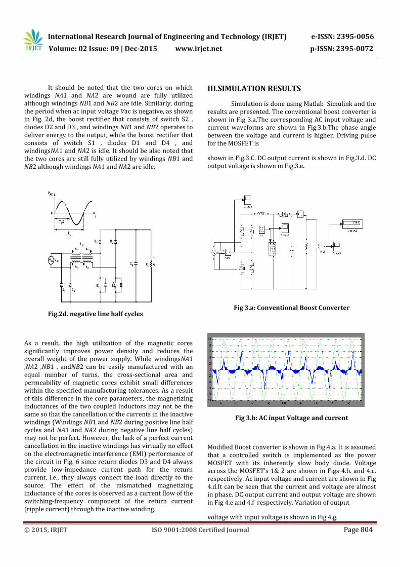
III.SIMULATION RESULTS
Simulation is done using Matlab Simulink and the results are presented. The conventional boost converter is shown in Fig 3.a.The corresponding AC input voltage and current waveforms are shown in Fig.3.b.The phase angle between the voltage and current is higher. Driving pulse for the MOSFET is
shown in Fig.3.C. DC output current is shown in Fig.3.d. DC output voltage is shown in Fig.3.e.
Fig 3.a: Conventional Boost Converter
Fig 3.b: AC input Voltage and current
Modified Boost converter is shown in Fig.4.a. It is assumed that a controlled switch is implemented as the power MOSFET with its inherently slow body diode. Voltage across the MOSFET’s 1& 2 are shown in Figs 4.b. and 4.c. respectively. Ac input voltage and current are shown in Fig 4.d.It can be seen that the current and voltage are almost in phase. DC output current and output voltage are shown in Fig 4.e and 4.f respectively. Variation of output
voltage with input voltage is shown in Fig 4.g.

International Research Journal of Engineering and Technology (IRJET) e-ISSN: 2395-0056
Volume: 02 Issue: 09 | Dec-2015 www.irjet.net p-ISSN: 2395-0072
© 2015, IRJET ISO 9001:2008 Certified Journal Page 805
Fig 3.c: Driving pulse for S1
Fig 3.d: DC output current
Fig 3.e: DC output Voltage
Open loop controlled boost converter circuit is shown in Fig 5.a. Step rise in input voltage is shown in Fig 5.b. DC output voltage also increases as shown in Fig 5.c. Closed loop system is shown in Fig 6.a. Output voltage is sensed and it is compared with a reference voltage. The error is processed through a PI controller. Step rise in input voltage for closed loop system is shown in Fig6.b.The output of the pulse generator controls the output voltage till it reaches the set value. It can be seen that the DC voltage reaches the set value as shown in Fig 6.c.
Fig 4.a: Modified Boost converter
Fig 4.b: Voltage across switch-1 and switch-2
Fig 4.d: AC input voltage and current
Fig 4.e: DC output current

International Research Journal of Engineering and Technology (IRJET) e-ISSN: 2395-0056
Volume: 02 Issue: 09 | Dec-2015 www.irjet.net p-ISSN: 2395-0072
© 2015, IRJET ISO 9001:2008 Certified Journal Page 806
Fig 4.f: DC output voltage
Fig: 4.g Input voltage vs. Output voltage
Fig 5.a: open loop controlled boost converter.
Fig 5.b: Input voltage.
Fig 5.c: DC output voltage.
Fig 6.b: Input Voltage.
Fig 6.a: Closed loop controlled boost converter.

International Research Journal of Engineering and Technology (IRJET) e-ISSN: 2395-0056
Volume: 02 Issue: 09 | Dec-2015 www.irjet.net p-ISSN: 2395-0072
© 2015, IRJET ISO 9001:2008 Certified Journal Page 807
Fig 6.c: Output Voltage
IV .CONCLUSION
Bridgeless PFC Converter with optimized magnetic utilization is modeled and simulated using Matlab. Open loop and closed loop models are developed and they are used successfully for simulation. The simulation studies indicate that the power factor is nearly unity by employing the modified boost converter. This converter has advantages like reduced hardware, high performance and improved power factor. The simulation results are in line with the predictions. This work has covered the simulation of open loop and closed loop controlled PFC converter. The hardware implementation will be done in future.
REFERENCES
[1]A Bridgeless PFC Boost Rectifier With Optimized Magnetic Utilization Yungtaek Jang, Senior Member, IEEE, and Milan M. Jovanovi´c,Fellow, IEEE TRANSACTIONS ON POWER ELECTRONICS, VOL. 24, NO. 1, JANUARY 2009.
[2] B. Lu, R. Brown, and M. Soldano, “Bridgeless PFC implementation using one cycle control technique,” in Proc. IEEE Appl. Power Electron. (APEC)Conf. Expo., Mar., 2005, pp. 812–817
[3] L. Huber, Y. Jang, and M. M. Jovanovic, “Performance evaluation of bridgeless PFC boost rectifiers,” IEEE Trans. Power Electron., vol. 23,no. 3, pp. 1381–1390, May 2008.
[4] H. Ye, Z. Yang, J. Dai, C. Yan, X. Xin, and J. Ying, “Common mode noise modeling and analysis of dual boost PFC circuit,” in Proc. Int.Telecommun. Energy Conf. (INTELEC), Sep. 2004, pp. 575–582.
[5]J. Sun, K. F. Webb, and V. Mehrotra, “Integrated magnetics for current doubler rectifiers,” IEEE Trans. Power Electron., vol. 19, no. 3, pp. 582–590, Nov. 2004.
[6]H. Ye, Z. Yang, J. Dai, C. Yan, X. Xin, and J. Ying, “Common mode noise modeling and analysis of dual boost PFC circuit,” in Proc. IntTelecommun. Energy Conf. (INTELEC), Sep. 2004, pp. 575–582.