cmos process variations eeprom fabrication …people.rit.edu/lffeee/eeprom.pdf · the eeprom is...
TRANSCRIPT
© February 22, 2012 Dr. Lynn Fuller, Professor
Rochester Institute of Technology
Microelectronic Engineering
EEPROM Technology
Page 1
ROCHESTER INSTITUTE OF TECHNOLOGYMICROELECTRONIC ENGINEERING
CMOS Process VariationsEEPROM Fabrication Technology
Dr. Lynn FullerWebpage: http://people.rit.edu/lffeee
Microelectronic EngineeringRochester Institute of Technology
82 Lomb Memorial DriveRochester, NY 14623-5604
Tel (585) 475-2035Email: [email protected]
Department Webpage: http://www.microe.rit.edu
2-22-2012 EEPROM.PPT

© February 22, 2012 Dr. Lynn Fuller, Professor
Rochester Institute of Technology
Microelectronic Engineering
EEPROM Technology
Page 2
OUTLINE
IntroductionTunneling Gate Oxide EEPROMProgrammingReadingTest Specification/ResultsFowler-Nordheim TunnelingProcess VariationTunnel Oxide RecipeTest Chip LayoutStep-by-Step Process

© February 22, 2012 Dr. Lynn Fuller, Professor
Rochester Institute of Technology
Microelectronic Engineering
EEPROM Technology
Page 3
INTRODUCTION
In certain applications, data must be electrically entered and erased from Read Only Memory (ROM). The procedure can involve the entire ROM sections or one memory cell at a time. From the various technologies available, we have chosen the design of a FLOTOX EEPROM (FLOating-gate Tunneling Oxide Electrically Erasable Programmable ROM, Figure 1.
This EEPROM cell has double polysilicon gates, with the top polysilicon as the control gate and the lower polysilicon as the floating gate. A thin tunneling
oxide is formed above the drain in the FLOTOX Transistor.

© February 22, 2012 Dr. Lynn Fuller, Professor
Rochester Institute of Technology
Microelectronic Engineering
EEPROM Technology
Page 4
TUNNELING GATE OXIDE EEPROM
Another form of the FLOTOX Transistor is shown below. The structure is simpler and smaller but is more difficult to manufacture because of the problems associated with diffusion of phosphorous from the gate poly through the tunnel oxide into the transistor channel region. Most modern EEPROM devices use this structure.
n+ n+
Gate DrainSource
P-well or P substrate
© February 22, 2012 Dr. Lynn Fuller, Professor
Rochester Institute of Technology
Microelectronic Engineering
EEPROM Technology
Page 5
INTRODUCTION
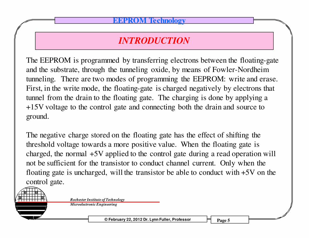
The EEPROM is programmed by transferring electrons between the floating-gate and the substrate, through the tunneling oxide, by means of Fowler-Nordheim tunneling. There are two modes of programming the EEPROM: write and erase. First, in the write mode, the floating-gate is charged negatively by electrons that tunnel from the drain to the floating gate. The charging is done by applying a +15V voltage to the control gate and connecting both the drain and source to ground.
The negative charge stored on the floating gate has the effect of shifting the threshold voltage towards a more positive value. When the floating gate is charged, the normal +5V applied to the control gate during a read operation will not be sufficient for the transistor to conduct channel current. Only when the floating gate is uncharged, will the transistor be able to conduct with +5V on the control gate.

© February 22, 2012 Dr. Lynn Fuller, Professor
Rochester Institute of Technology
Microelectronic Engineering
EEPROM Technology
Page 6
PROGRAMMING THE EEPROM CELL
WordBit
Ctrl
0V
15V
0V
Write a 1Leave Electronson Floating Gate
WordBit
Ctrl
15V
0V
15V
Precharge FloatingGate with Electrons
WordBit
Ctrl
0V
15V
15V
Write a 0Remove ElectronsFrom Floating Gate

© February 22, 2012 Dr. Lynn Fuller, Professor
Rochester Institute of Technology
Microelectronic Engineering
EEPROM Technology
Page 7
READING THE CELL
WordBitLine
Control
5V
5V
5V
Read Output
If the floating gate is charged with electrons the 5 volts on the control line will not be enough to turn that transistor on. Thus the output will be high.
If the floating gate is uncharged with electrons the 5 volts on the control line will turn that transistor on. Thus the output will be low.
R

© February 22, 2012 Dr. Lynn Fuller, Professor
Rochester Institute of Technology
Microelectronic Engineering
EEPROM Technology
Page 8
TEST SPECIFICATION
SpecificationCan FLOTOX Transistor be programmed
Charge the Floating GateMeasure the subthreshold characteristicsDischarge the Floating GateMeasure the subthreshold characteristics
Can the FLOTOX Transistor hold the chargeCharge the Floating GateMeasure the subthreshold characteristicsWait 1hours, 10 hours, 100 hours, 1000hoursMeasure the subthreshold characteristics
Can the FLOTOX Transistor be cycled many timesHow much time does it take to charge and discharge

© February 22, 2012 Dr. Lynn Fuller, Professor
Rochester Institute of Technology
Microelectronic Engineering
EEPROM Technology
Page 9
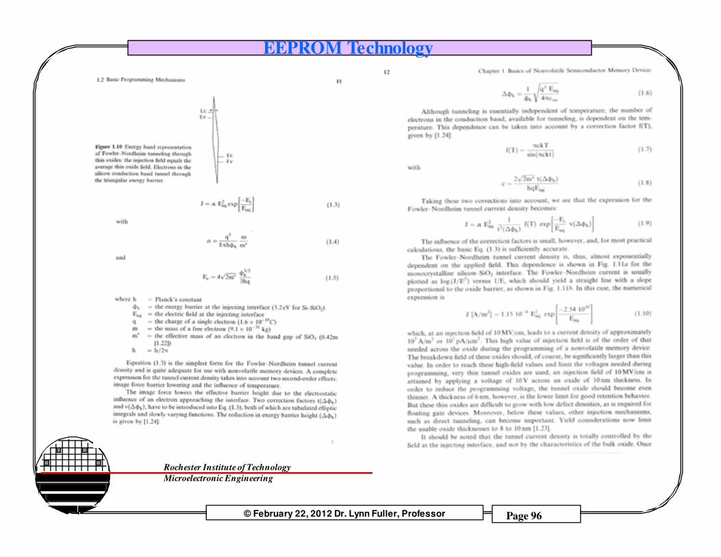
FOWLER-NORDHEIM TUNNELING
J = C1 Ec2 exp(-Eo/Ec)
C1 = q3 m / (8πhφb m*) = 9.625E-7 A/V2
Ec = VFG/toxEo = 8π(2m)1/2 φb
3/2 /(3hq)
VFG =
Vp C G /(CG + CFG)
VP
CG
CFG
Example: let CFG=0.3 pF, CG=0.2 pF, Vp=25 volts, tox = 100 Å, m*=.5me , φb = 3.2where me=9.11E-31, h=(6.625E-34)/2π, q=1.6E-19
so Eo=2.765E8 V/cm and Ec = 10/100E-8 V/cm
J = 9.625E-7 (Ec)2 exp (-2.765E8/Ec)=94.4 µA/cm2
© February 22, 2012 Dr. Lynn Fuller, Professor
Rochester Institute of Technology
Microelectronic Engineering
EEPROM Technology
Page 10
CMOS PROCESS MODIFICATIONS
The fabrication of a FLOTOX EEPROM involves a three modifications to the present CMOS process. An additional n+ drain implant is performed before the polysilicon layers are deposited. A thin 100 Å tunneling oxide is grown above the additional n+ implant region. A second polysilicon layer is deposited for the control gate.

© February 22, 2012 Dr. Lynn Fuller, Professor
Rochester Institute of Technology
Microelectronic Engineering
EEPROM Technology
Page 11
TUNNEL OXIDE RECIPE FOR ~120 Å SiO2
Step Gas Flow Temperature Time Boat0 Load Tube N2 @ 15 lpm 650 °C ? Out1 Push N2 @ 15 lpm 650 °C 15 min In2 Stabilization N2 @ 15 lpm 650 °C 15 min3 Ramp Up N2 @ 15 lpm 650 to 950 °C 30 min4 First Oxide N2 @ 15 lpm + O2 @ 5 lpm 950 °C 15 min5 First Anneal N2 @ 15 lpm 1050 °C 30 min6 Ramp Down N2 @ 15 lpm 950 °C 20 min7 2nd Oxide N2 @ 15 lpm + O2 @ 5 lpm 950 °C 10 min8 2nd Anneal N2 @ 15 lpm 950 °C 30 min9 Ramp Down N2 @ 15 lpm 950 to 650 °C 60 min10 Pull N2 @ 15 lpm 650 °C 15 min Out

© February 22, 2012 Dr. Lynn Fuller, Professor
Rochester Institute of Technology
Microelectronic Engineering
EEPROM Technology
Page 12
Entire Test Chip
EEPROM TransistorEEPROM plus SelectEEPROM Memory Array Variable Programmable
ResistorBinary-weighted Variable
ProgrammableResistor
ResistorsCapacitors

© February 22, 2012 Dr. Lynn Fuller, Professor
Rochester Institute of Technology
Microelectronic Engineering
EEPROM Technology
Page 13
EEPROM Transistor
Basic transistor with two layerspoly, tunnel oxide, and 3 connections.
Gate
Drain
Source

© February 22, 2012 Dr. Lynn Fuller, Professor
Rochester Institute of Technology
Microelectronic Engineering
EEPROM Technology
Page 14
Gate
Drain
Select
Source
EEPROM Transistor + Select
Basic transistor with two layerspoly, tunnel oxide, and 4 connections.

© February 22, 2012 Dr. Lynn Fuller, Professor
Rochester Institute of Technology
Microelectronic Engineering
EEPROM Technology
Page 15
EEPROM
Word Line 0
Bit Lines
Control/Read
5VR R R R
Word Line 1
Word Line 2
Word Line 3
Control/Read
Control/Read
Control/Read
B3 B2 B1 B0

© February 22, 2012 Dr. Lynn Fuller, Professor
Rochester Institute of Technology
Microelectronic Engineering
EEPROM Technology
Page 16
Memory array of four-by-four EEPROM cells
© February 22, 2012 Dr. Lynn Fuller, Professor
Rochester Institute of Technology
Microelectronic Engineering
EEPROM Technology
Page 17
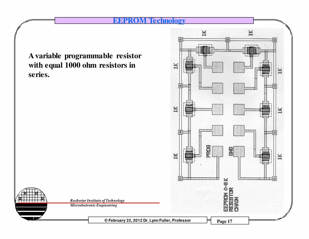
A variable programmable resistorwith equal 1000 ohm resistors inseries.
© February 22, 2012 Dr. Lynn Fuller, Professor
Rochester Institute of Technology
Microelectronic Engineering
EEPROM Technology
Page 18
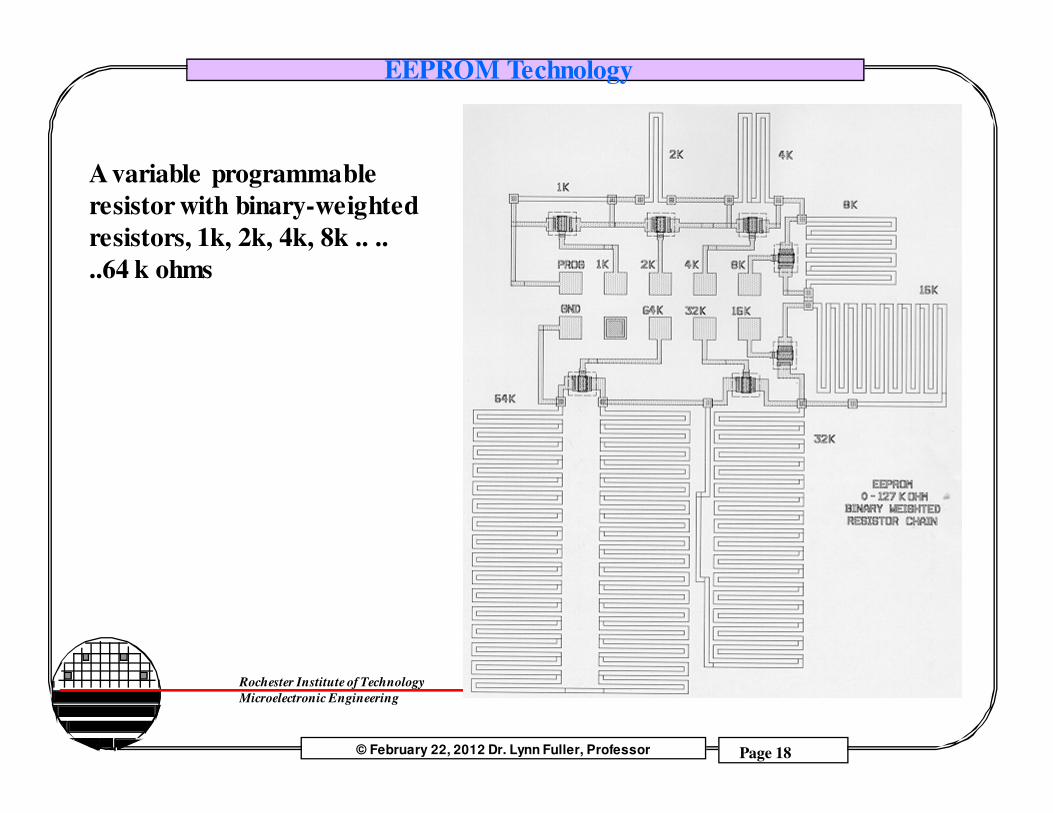
A variable programmable resistor with binary-weighted resistors, 1k, 2k, 4k, 8k .. .. ..64 k ohms
© February 22, 2012 Dr. Lynn Fuller, Professor
Rochester Institute of Technology
Microelectronic Engineering
EEPROM Technology
Page 19
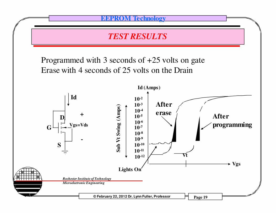
TEST RESULTS
Programmed with 3 seconds of +25 volts on gateErase with 4 seconds of 25 volts on the Drain
G
D
S
Vgs=Vds
Id
+
-
Id (Amps)
10-5
Vgs
Vt
10-410-310-2
10-1010-910-810-710-6
10-11
10-12
Lights On
Sub
Vt
Swin
g (A
mps
)Afterprogramming
Aftererase
© February 22, 2012 Dr. Lynn Fuller, Professor
Rochester Institute of Technology
Microelectronic Engineering
EEPROM Technology
Page 20
REFERENCES
1. “Flash EE PROM Device”, Keith Zawadski, Senior Desing Project, May 1996.
2. “EEPROMs”, Edward Storbeck, Visiting Scholar from South Africa, 1996-97.
3. Device Electronics for Integrated Circuits, Richard S. Muller, Theodore I. Kamins, John Wiley and Sons, Inc.
4. Nonvolatile Semiconductor Memory Technology, Edited by William D. Brown and Joe E. Brewer, IEEE Press
© February 22, 2012 Dr. Lynn Fuller, Professor
Rochester Institute of Technology
Microelectronic Engineering
EEPROM Technology
Page 21
HOMEWORK - EEPROM
1.0 Calculate the current that would flow through a 10 by 10 µm tunnel oxide of 100 Å, at a control gate voltage of 10, 15 and 20 Volts, assume CFG=0.3pF and CG=0.2 pF
2.0 How long would it take to charge the floating gate to 2.5 volts. Assume the floating gate is 0.3 pF floating gate and the currents are as found in problem 1.0.
3.0 Describe the exact procedure that you would use to test the FLOTOX transistor.

© February 22, 2012 Dr. Lynn Fuller, Professor
Rochester Institute of Technology
Microelectronic Engineering
EEPROM Technology
Page 22
HOMEWORK - EEPROM
1.0 Calculate the current that would flow through a 10 by 10 µm tunnel oxide of 100 Å, at a control gate voltage of 10, 15 and 20 Volts, assume CFG=0.3pF and CG=0.2 pF
2.0 How long would it take to charge the floating gate to 2.5 volts. Assume the floating gate is 0.3 pF floating gate and the currents are as found in problem 1.0.
3.0 Describe the exact procedure that you would use to test the FLOTOX transistor.
© February 22, 2012 Dr. Lynn Fuller, Professor
Rochester Institute of Technology
Microelectronic Engineering
EEPROM Technology
Page 23
NOR AND NAND FLASH
Flash memory is a non-volatile computer storage that can be electrically erased and reprogrammed. It is a technology that is primarily used in memory cards and USB flash drives for general storage and transfer of data between computers and other digital products. It is a specific type of EEPROM (Electrically Erasable Programmable Read-Only Memory) that is erased and programmed in large blocks; in early flash the entire chip had to be erased at once. Flash memory costs far less than byte-programmable EEPROM and therefore has become the dominant technology wherever a significant amount of non-volatile, solid state storage is needed. Example applications include PDAs (personal digital assistants), laptop computers, digital audio players, digital cameras and mobile phones. It has also gained popularity in console video game hardware, where it is often used instead of EEPROMs or battery-powered static RAM (SRAM) for game save data.
Since flash memory is non-volatile, no power is needed to maintain the information stored in the chip. In addition, flash memory offers fast read access times (although not as fast as volatile DRAM memory used for main memory in PCs) and better kinetic shock resistance than hard disks. These characteristics explain the popularity of flash memory in portable devices. Another feature of flash memory is that when packaged in a "memory card," it is extremely durable, being able to withstand intense pressure, extremes of temperature, and even immersion in water.Although technically a type of EEPROM, the term "EEPROM" is generally used to refer specifically to non-flash EEPROM which is erasable in small blocks, typically bytes. Because erase cycles are slow, the large block sizes used in flash memory erasing give it a significant speed advantage over old-style EEPROM when writing large amounts of data.
Wikipedia contributors. "Flash memory." Wikipedia, The Free Encyclopedia. Wikipedia, The Free Encyclopedia, 3 Feb. 2010. Web. 11 Feb. 2010.
© February 22, 2012 Dr. Lynn Fuller, Professor
Rochester Institute of Technology
Microelectronic Engineering
EEPROM Technology
Page 24
NOR AND NAND FLASH
NOR and NAND flash differ in two important ways: the connections of the individual memory cells are different the interface provided for reading and writing the memory is different (NOR allows random-access for reading, NAND allows only page access) These two are linked by the design choices made in the development of NAND flash. A goal of NAND flash development was to reduce the chip area required to implement a given capacity of flash memory, and thereby to reduce cost per bit and increase maximum chip capacity so that flash memory could compete with magnetic storage devices like hard disks. NOR and NAND flash get their names from the structure of the interconnections between memory cells. In NOR flash, cells are connected in parallel to the bitlines, allowing cells to be read and programmed individually. The parallel connection of cells resembles the parallel connection of transistors in a CMOS NOR gate. In NAND flash, cells are connected in series, resembling a NAND gate. The series connections consume less space than parallel ones, reducing the cost of NAND flash. It does not, by itself, prevent NAND cells from being read and programmed individually. When NOR flash was developed, it was envisioned as a more economical and conveniently rewritable ROM than contemporary EPROM, EAROM, and EEPROM memories. Thus random-access reading circuitry was necessary. However, it was expected that NOR flash ROM would be read much more often than written, so the write circuitry included was fairly slow and could only erase in a block-wise fashion. On the other hand, applications that use flash as a replacement for disk drives do not require word-level write address, which would only add to the complexity and cost unnecessarily. Because of the series connection and removal of wordline contacts, a large grid of NAND flash memory cells will occupy perhaps only 60% of the area of equivalent NOR cells (assuming the same CMOS process resolution, e.g. 130nm, 90 nm, 65 nm). NAND flash's designers realized that the area of a NAND chip, and thus the cost, could be further reduced by removing the external address and data bus circuitry. Instead, external devices could communicate with NAND flash via sequential-accessed command and data registers, which would internally retrieve and output the necessary data. This design choice made random-access of NAND flash memory impossible, but the goal of NAND flash was to replace hard disks, not to replace ROMs.
Wikipedia contributors. "Flash memory." Wikipedia, The Free Encyclopedia. Wikipedia, The Free Encyclopedia, 3 Feb. 2010. Web. 11 Feb. 2010.
© February 22, 2012 Dr. Lynn Fuller, Professor
Rochester Institute of Technology
Microelectronic Engineering
EEPROM Technology
Page 25

© February 22, 2012 Dr. Lynn Fuller, Professor
Rochester Institute of Technology
Microelectronic Engineering
EEPROM Technology
Page 26
132GBit NAND FLASH
© February 22, 2012 Dr. Lynn Fuller, Professor
Rochester Institute of Technology
Microelectronic Engineering
EEPROM Technology
Page 27
© February 22, 2012 Dr. Lynn Fuller, Professor
Rochester Institute of Technology
Microelectronic Engineering
EEPROM Technology
Page 28
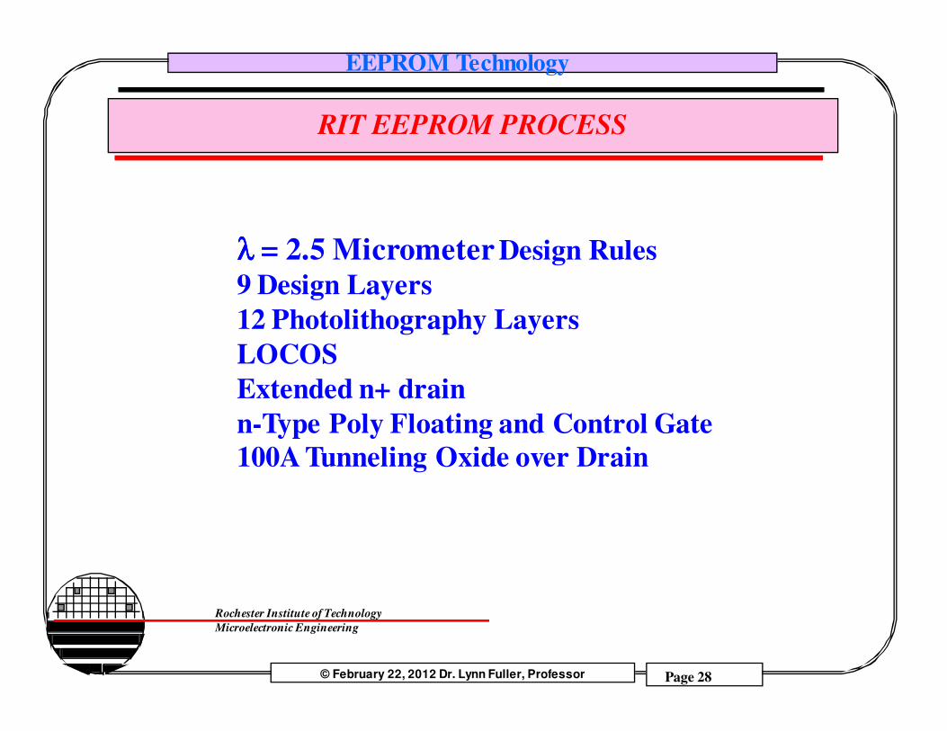
RIT EEPROM PROCESS
λλλλ = 2.5 Micrometer Design Rules9 Design Layers12 Photolithography LayersLOCOSExtended n+ drainn-Type Poly Floating and Control Gate100A Tunneling Oxide over Drain
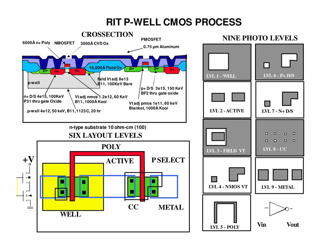
RIT P-WELL CMOS PROCESS
NINE PHOTO LEVELS
LVL 1 - WELL
LVL 9 - METALLVL 4 - NMOS VT
LVL 7 - N+ D/SLVL 2 - ACTIVE
LVL 6 - P+ D/S
LVL 3 - FIELD VT LVL 8 - CC
LVL 5 - POLY
POLY
METALWELL
P SELECT
CC
ACTIVE
CROSSECTION
SIX LAYOUT LEVELS
NMOSFETPMOSFET
p-well
p+ p+p+ n+n+ n+
p-well 4e12, 50 keV, B11, 1123 C, 20 hr
10,000Å Field Ox
3000Å CVD Ox0.75 µm Aluminum
p+ D/S 2e15, 150 KeVBF2 thru gate oxide
n+ D/S 4e15, 100KeVP31 thru gate Oxide
Vt adj nmos 1.2e12, 60 KeVB11, 1000Å Kooi Vt adj pmos 1e11, 60 keV
Blanket, 1000Å Kooi
field Vt adj 8e13B11, 100KeV Bare
6000Å n+ Poly
n-type substrate 10 ohm-cm (100)
Vin Vout
+V

© February 22, 2012 Dr. Lynn Fuller, Professor
Rochester Institute of Technology
Microelectronic Engineering
EEPROM Technology
Page 30
CROSS-SECTION
EEPROM NMOS
Vt adj blanket and nmose , 60 KeV B11, 1000Å Kooi
field Vt adj 8e13B11, 100KeV Bare
p+ D/S 4e15, 120 KeVBF2 into bare silicon
n+ D/S 4e15, 100KeVP31 thru gate Oxide
p-well 4e12, 50 keV, B11, 1123 C, 20 hr
n+ D/S 4e15, 100KeVP31 thru gate Oxide
n+ n+ n+p+ n+
Three extra layers: Drain ExtensionTunnel OxideFloating Poly

© February 22, 2012 Dr. Lynn Fuller, Professor
Rochester Institute of Technology
Microelectronic Engineering
EEPROM Technology
Page 31
F960417
D1
V
I
Rho = V / I * Pi / ln 2 ohm-cm
IDENTIFY AND FOUR POINT PROBE
N-TYPE WAFER, 10 OHM CM

© February 22, 2012 Dr. Lynn Fuller, Professor
Rochester Institute of Technology
Microelectronic Engineering
EEPROM Technology
Page 32
ALIGNMENT OXIDEEEPROM NMOS
n-type substrate, 5-15 ohm-cm, (100)
Well Oxide, 5000 ÅPush, 12 in/min at 900 C, 5 lmp N2
Ramp to 1100 C, 5 lpm Dry O2
Soak for 48 min, 5 lpm wet O2
Ramp to 1000 C, 5 lpm N2
Pull, 12 in/min, 5 lpm N2

© February 22, 2012 Dr. Lynn Fuller, Professor
Rochester Institute of Technology
Microelectronic Engineering
EEPROM Technology
Page 33
EEPROM NMOS
Photoresist
well Oxide, 5000 Å
n-type substrate, 5-15 ohm-cm, (100)
LEVEL 1 PHOTO - WELL
© February 22, 2012 Dr. Lynn Fuller, Professor
Rochester Institute of Technology
Microelectronic Engineering
EEPROM Technology
Page 34
EEPROM NMOS
OXIDE ETCH

© February 22, 2012 Dr. Lynn Fuller, Professor
Rochester Institute of Technology
Microelectronic Engineering
EEPROM Technology
Page 35
EEPROM NMOS
p-well implant, 4e12, 50 KeV, B11
WELL IMPLANT

© February 22, 2012 Dr. Lynn Fuller, Professor
Rochester Institute of Technology
Microelectronic Engineering
EEPROM Technology
Page 36
STRIP RESISTEEPROM NMOS
p-well implant, 4e12, 50 KeV, B11
© February 22, 2012 Dr. Lynn Fuller, Professor
Rochester Institute of Technology
Microelectronic Engineering
EEPROM Technology
Page 37
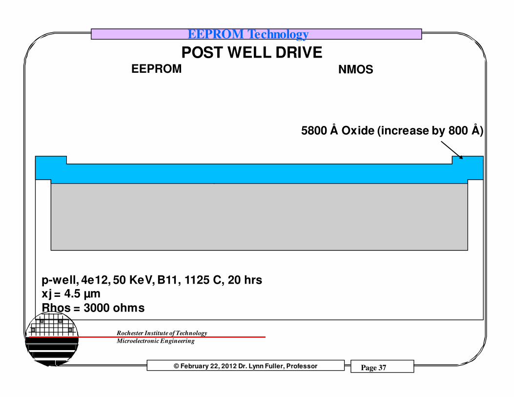
EEPROM NMOS
5800 Å Oxide (increase by 800 Å)
2850 Å Oxide, 4 hours Dry O2
POST WELL DRIVE
p-well, 4e12, 50 KeV, B11, 1125 C, 20 hrsxj = 4.5 µmRhos = 3000 ohms
© February 22, 2012 Dr. Lynn Fuller, Professor
Rochester Institute of Technology
Microelectronic Engineering
EEPROM Technology
Page 38
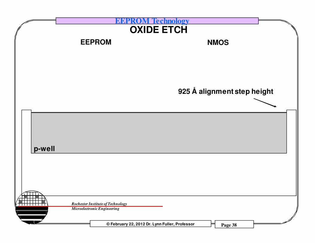
EEPROM NMOS
p-well
OXIDE ETCH
925 Å alignment step height

© February 22, 2012 Dr. Lynn Fuller, Professor
Rochester Institute of Technology
Microelectronic Engineering
EEPROM Technology
Page 39
EEPROM NMOS
p-well
GROW PAD OXIDE
Well Oxide, 500 ÅPush, 12 in/min at 900 C, N2
Ramp to 1100 , Dry O2
Soak for 8 min, Dry O2
Ramp down to 1000 C, N2
Pull, 12 in/mi, N2
© February 22, 2012 Dr. Lynn Fuller, Professor
Rochester Institute of Technology
Microelectronic Engineering
EEPROM Technology
Page 40
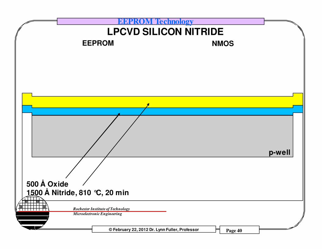
EEPROM NMOS
p-well
LPCVD SILICON NITRIDE
500 Å Oxide1500 Å Nitride, 810 °C, 20 min

© February 22, 2012 Dr. Lynn Fuller, Professor
Rochester Institute of Technology
Microelectronic Engineering
EEPROM Technology
Page 41
EEPROM NMOS
p-well
photoresist
LEVEL 2 PHOTO - ACTIVE
10,000 Å

© February 22, 2012 Dr. Lynn Fuller, Professor
Rochester Institute of Technology
Microelectronic Engineering
EEPROM Technology
Page 42
EEPROM NMOS
p-well
NITRIDE PLASMA ETCH
SF6, 300 mTorr, 30 sccm50 W, 60 seconds
© February 22, 2012 Dr. Lynn Fuller, Professor
Rochester Institute of Technology
Microelectronic Engineering
EEPROM Technology
Page 43
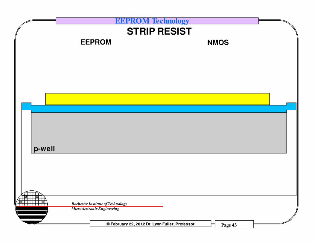
STRIP RESISTEEPROM NMOS
p-well

© February 22, 2012 Dr. Lynn Fuller, Professor
Rochester Institute of Technology
Microelectronic Engineering
EEPROM Technology
Page 44
EEPROM NMOS
p-well
LEVEL 3 PHOTO - CHANNEL STOP / FIELD VT ADJ

© February 22, 2012 Dr. Lynn Fuller, Professor
Rochester Institute of Technology
Microelectronic Engineering
EEPROM Technology
Page 45
EEPROM NMOS
p-well
IMPLANT CHANNEL STOPS
11B
11B, 100 keV, 8E13
© February 22, 2012 Dr. Lynn Fuller, Professor
Rochester Institute of Technology
Microelectronic Engineering
EEPROM Technology
Page 46
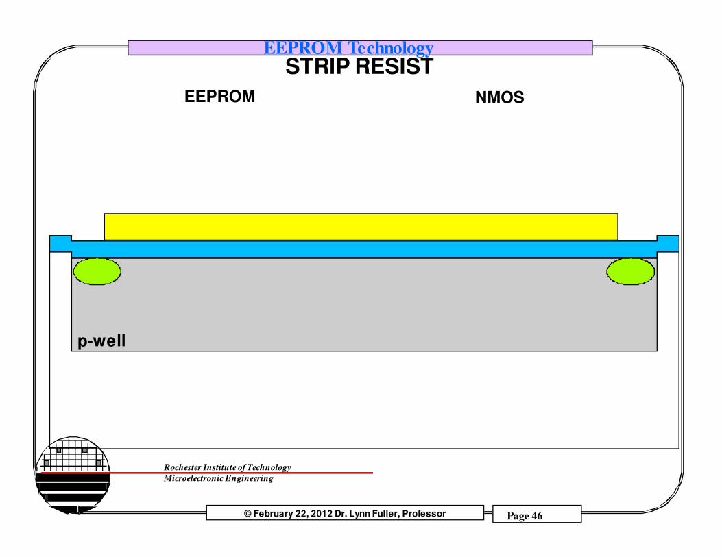
STRIP RESISTEEPROM NMOS
p-well

© February 22, 2012 Dr. Lynn Fuller, Professor
Rochester Institute of Technology
Microelectronic Engineering
EEPROM Technology
Page 47
OXIDE ETCHEEPROM NMOS
p-well
1 min in BOE HF

© February 22, 2012 Dr. Lynn Fuller, Professor
Rochester Institute of Technology
Microelectronic Engineering
EEPROM Technology
Page 48
GROW FIELD OXIDEEEPROM NMOS
p-well
Push in 900C, ramp to 1100C in O2,soak 210 min wet O2, ramp down to 1000C and pull.

© February 22, 2012 Dr. Lynn Fuller, Professor
Rochester Institute of Technology
Microelectronic Engineering
EEPROM Technology
Page 49
NITRIDE ETCHEEPROM NMOS
p-well

© February 22, 2012 Dr. Lynn Fuller, Professor
Rochester Institute of Technology
Microelectronic Engineering
EEPROM Technology
Page 50
OXIDE ETCHEEPROM NMOS
p-well

© February 22, 2012 Dr. Lynn Fuller, Professor
Rochester Institute of Technology
Microelectronic Engineering
EEPROM Technology
Page 51
GROW KOOI OXIDEEEPROM NMOS
p-well

© February 22, 2012 Dr. Lynn Fuller, Professor
Rochester Institute of Technology
Microelectronic Engineering
EEPROM Technology
Page 52
IMPLANT BLANKET Vt ADJEEPROM NMOS
p-well
11B, 60 keV, 0e12

© February 22, 2012 Dr. Lynn Fuller, Professor
Rochester Institute of Technology
Microelectronic Engineering
EEPROM Technology
Page 53
LEVEL 4 PHOTO - NMOS Vt ADJEEPROM NMOS
p-well

© February 22, 2012 Dr. Lynn Fuller, Professor
Rochester Institute of Technology
Microelectronic Engineering
EEPROM Technology
Page 54
IMPLANT - NMOS Vt ADJEEPROM NMOS
p-well
11B, 60 keV, 1.2e12
© February 22, 2012 Dr. Lynn Fuller, Professor
Rochester Institute of Technology
Microelectronic Engineering
EEPROM Technology
Page 55
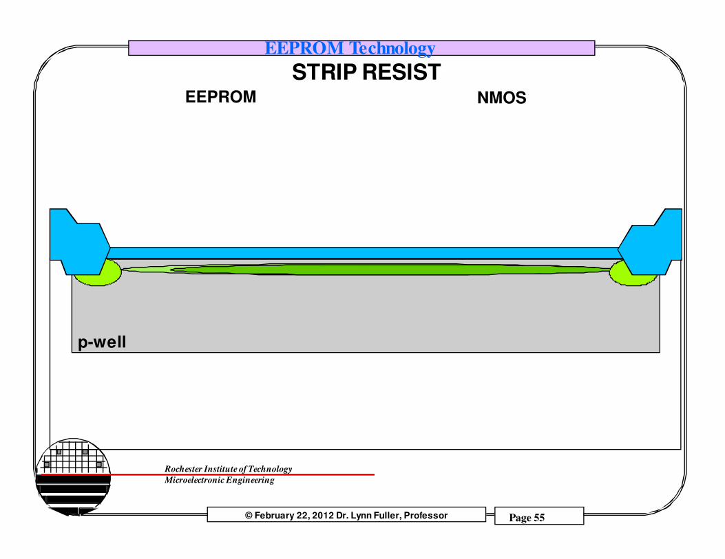
STRIP RESISTEEPROM NMOS
p-well
© February 22, 2012 Dr. Lynn Fuller, Professor
Rochester Institute of Technology
Microelectronic Engineering
EEPROM Technology
Page 56
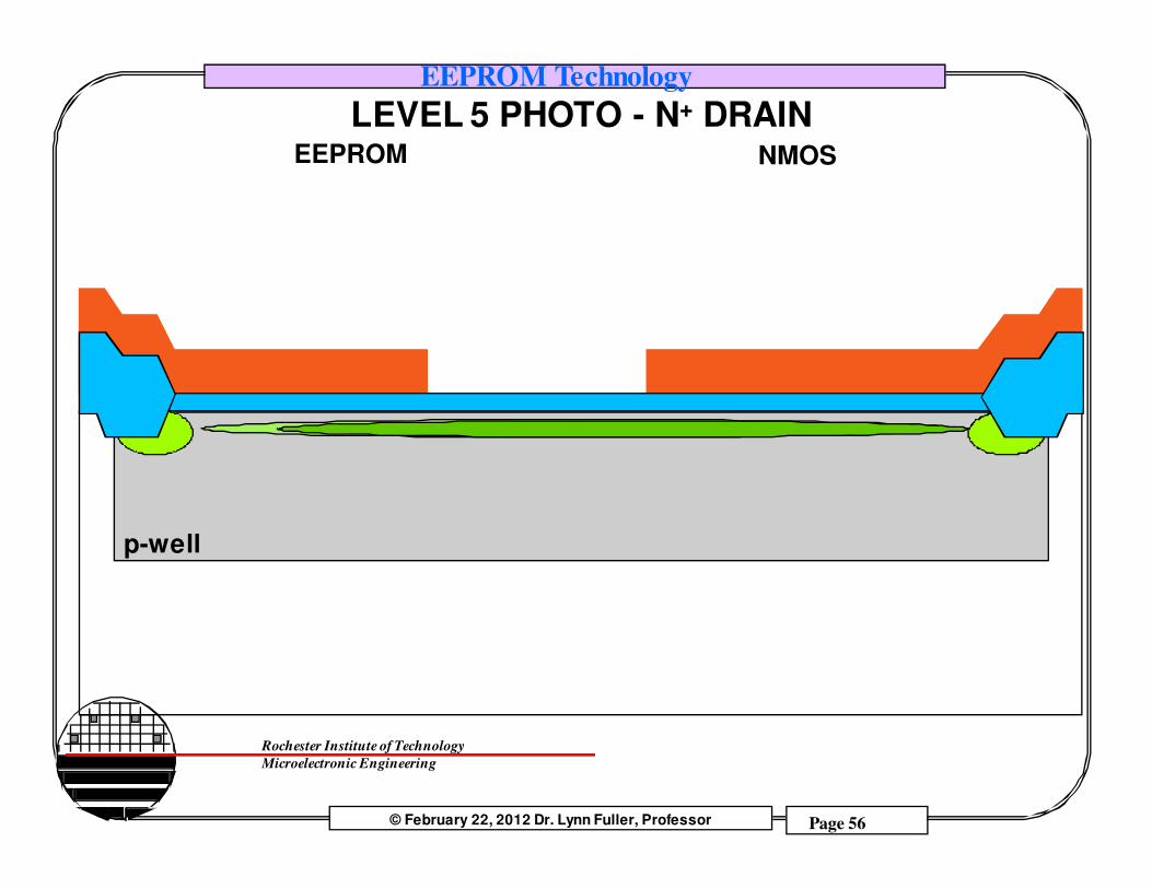
LEVEL 5 PHOTO - N+ DRAINEEPROM NMOS
p-well

© February 22, 2012 Dr. Lynn Fuller, Professor
Rochester Institute of Technology
Microelectronic Engineering
EEPROM Technology
Page 57
IMPLANT N+ DRAINEEPROM NMOS
p-well
31P, 100 keV, 4e15

© February 22, 2012 Dr. Lynn Fuller, Professor
Rochester Institute of Technology
Microelectronic Engineering
EEPROM Technology
Page 58
STRIP RESISTEEPROM NMOS
p-well
n+
© February 22, 2012 Dr. Lynn Fuller, Professor
Rochester Institute of Technology
Microelectronic Engineering
EEPROM Technology
Page 59
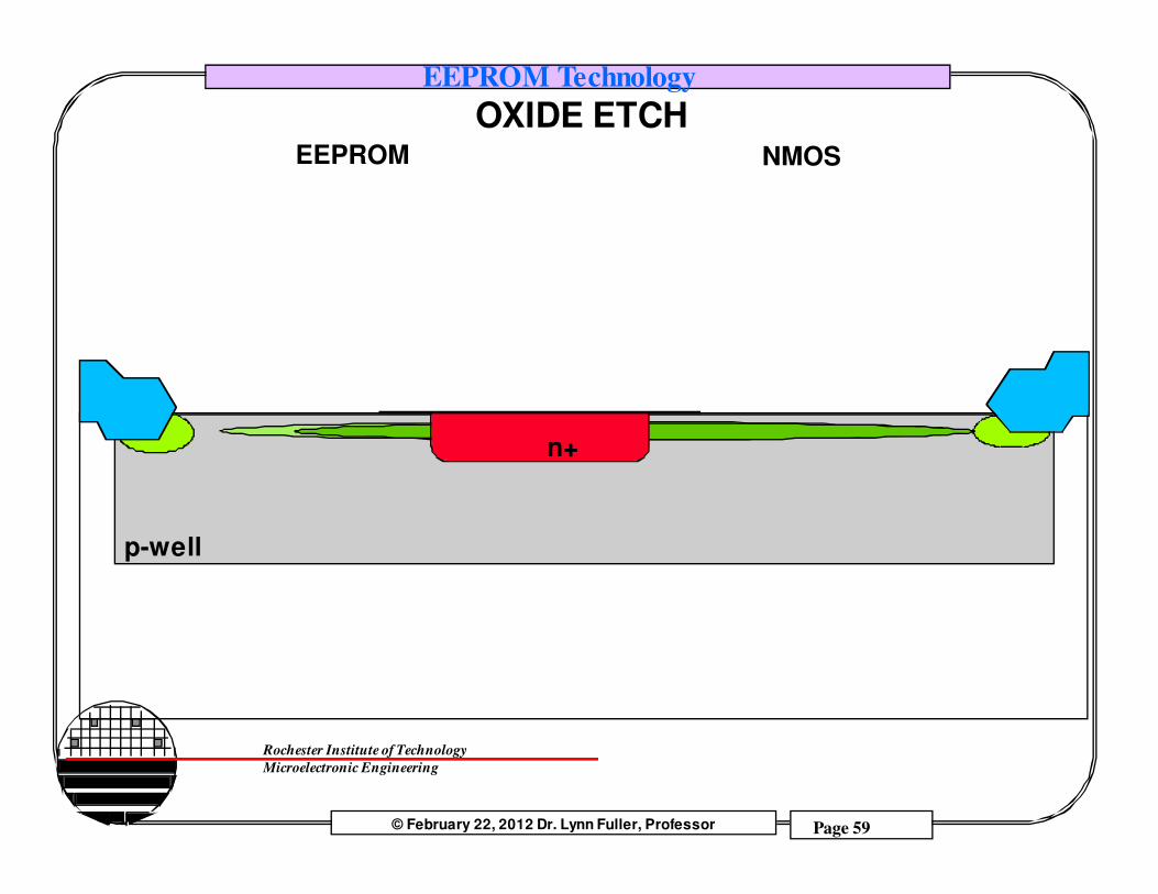
OXIDE ETCHEEPROM NMOS
p-well
n+

© February 22, 2012 Dr. Lynn Fuller, Professor
Rochester Institute of Technology
Microelectronic Engineering
EEPROM Technology
Page 60
EEPROM NMOS
n+
GROW GATE OXIDE
TCA tube clean during warm upPush at 900 C, 12 in/min, N2Ramp up to 1100 °C, dry O2Soak 1100 C, dry O2, 8 minPull at 900 C, 12 in/min, N2Xox desired = 500 Å

© February 22, 2012 Dr. Lynn Fuller, Professor
Rochester Institute of Technology
Microelectronic Engineering
EEPROM Technology
Page 61
EEPROM NMOS
p-well
n+
PHOTO 6 - TUNNEL OXIDE

© February 22, 2012 Dr. Lynn Fuller, Professor
Rochester Institute of Technology
Microelectronic Engineering
EEPROM Technology
Page 62
ET06EEPROM
NMOS
p-well
n+

© February 22, 2012 Dr. Lynn Fuller, Professor
Rochester Institute of Technology
Microelectronic Engineering
EEPROM Technology
Page 63
ET07EEPROM
NMOS
p-well
n+
© February 22, 2012 Dr. Lynn Fuller, Professor
Rochester Institute of Technology
Microelectronic Engineering
EEPROM Technology
Page 64
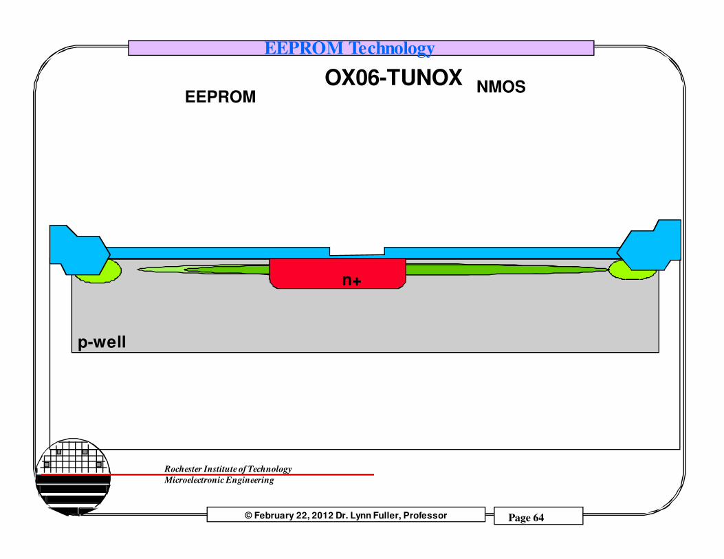
OX06-TUNOXEEPROM
NMOS
p-well
n+

© February 22, 2012 Dr. Lynn Fuller, Professor
Rochester Institute of Technology
Microelectronic Engineering
EEPROM Technology
Page 65
EEPROM NMOS
p-well
n+
POLYSILICON DEPOSITION
LPCVD Polysilicon0.6 micrometers610 °C, 60 min
© February 22, 2012 Dr. Lynn Fuller, Professor
Rochester Institute of Technology
Microelectronic Engineering
EEPROM Technology
Page 66
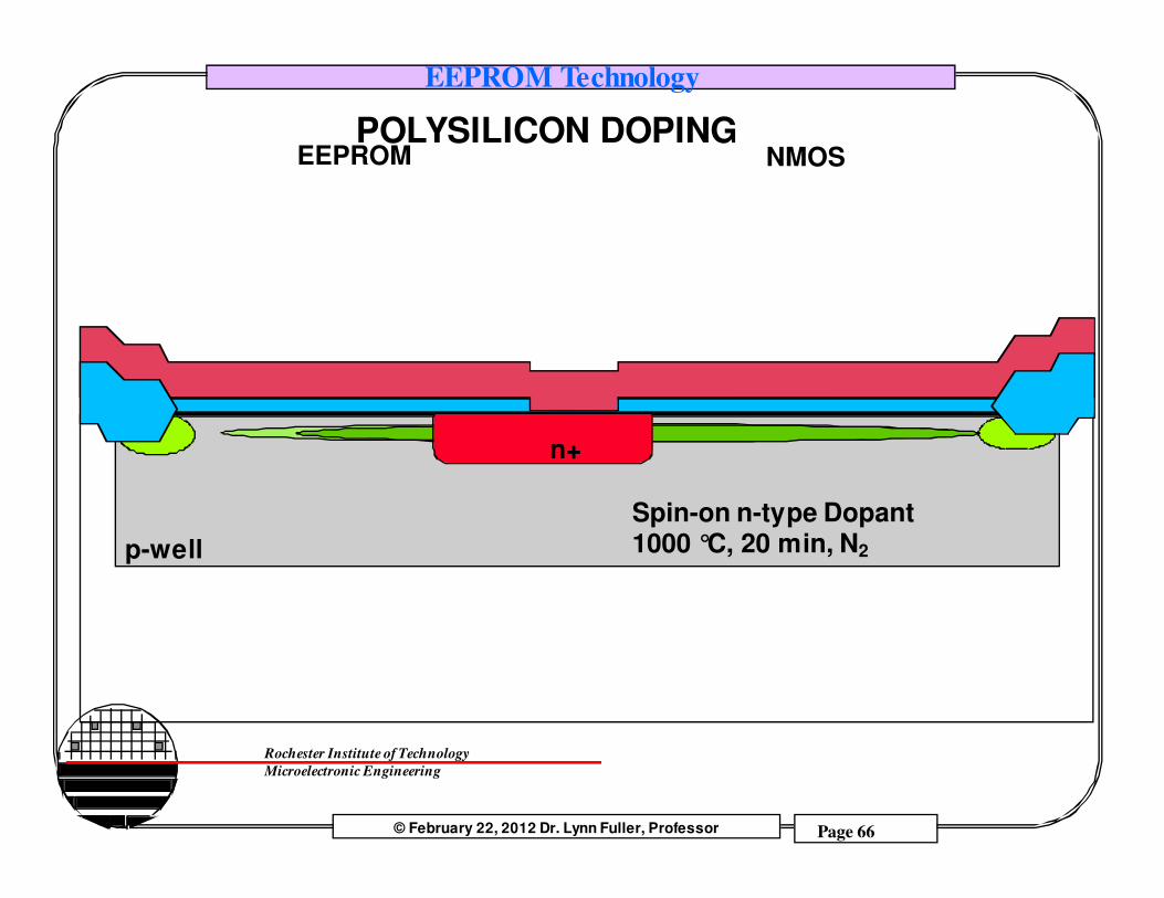
EEPROM NMOS
p-well
n+
POLYSILICON DOPING
Spin-on n-type Dopant1000 °C, 20 min, N2

© February 22, 2012 Dr. Lynn Fuller, Professor
Rochester Institute of Technology
Microelectronic Engineering
EEPROM Technology
Page 67
EEPROM NMOS
p-well
n+
ET06
Spin-on n-type Dopant1000 °C, 20 min, N2

© February 22, 2012 Dr. Lynn Fuller, Professor
Rochester Institute of Technology
Microelectronic Engineering
EEPROM Technology
Page 68
EEPROM NMOS
p-well
n+
LEVEL 5 PHOTO - POLYSILICON

© February 22, 2012 Dr. Lynn Fuller, Professor
Rochester Institute of Technology
Microelectronic Engineering
EEPROM Technology
Page 69
EEPROM NMOS
p-well
n+
PLASMA ETCH POLYSILICON
SF6 + O2, 30 sccm + 3 sccm, 75 mT, 75 watts

© February 22, 2012 Dr. Lynn Fuller, Professor
Rochester Institute of Technology
Microelectronic Engineering
EEPROM Technology
Page 70
EEPROM NMOS
p-well
n+
ET07
SF6 + O2, 30 sccm + 3 sccm, 75 mT, 75 watts

© February 22, 2012 Dr. Lynn Fuller, Professor
Rochester Institute of Technology
Microelectronic Engineering
EEPROM Technology
Page 71
ET06EEPROM
NMOS
p-well
n+

© February 22, 2012 Dr. Lynn Fuller, Professor
Rochester Institute of Technology
Microelectronic Engineering
EEPROM Technology
Page 72
CL01 & OX06EEPROM
NMOS
p-well
n+

© February 22, 2012 Dr. Lynn Fuller, Professor
Rochester Institute of Technology
Microelectronic Engineering
EEPROM Technology
Page 73
CV01EEPROM
NMOS
p-well
n+
© February 22, 2012 Dr. Lynn Fuller, Professor
Rochester Institute of Technology
Microelectronic Engineering
EEPROM Technology
Page 74
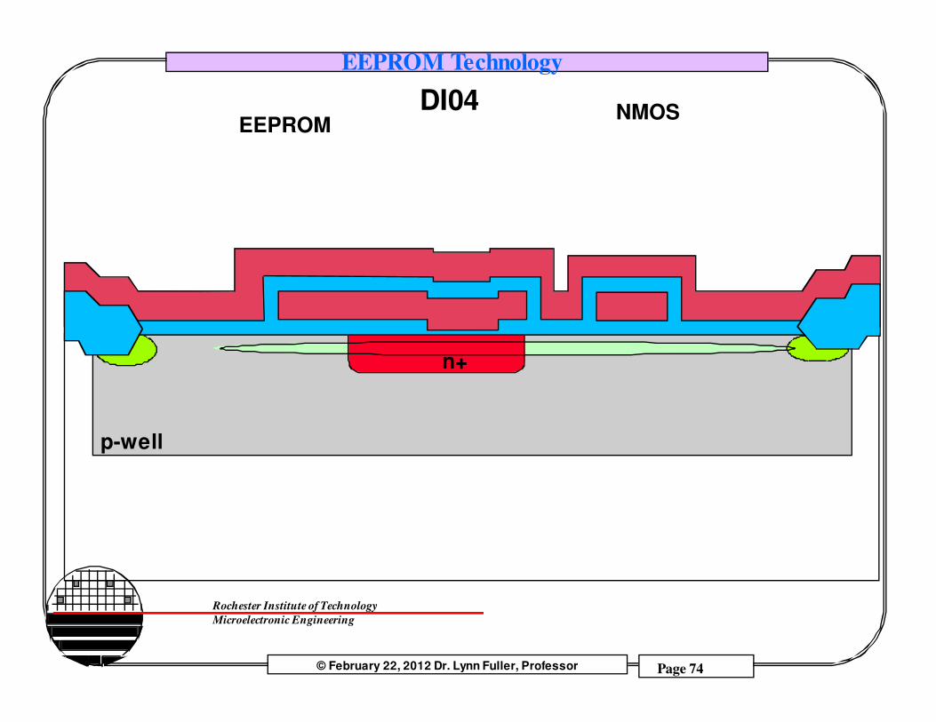
DI04EEPROM
NMOS
p-well
n+

© February 22, 2012 Dr. Lynn Fuller, Professor
Rochester Institute of Technology
Microelectronic Engineering
EEPROM Technology
Page 75
ET06EEPROM
NMOS
p-well
n+

© February 22, 2012 Dr. Lynn Fuller, Professor
Rochester Institute of Technology
Microelectronic Engineering
EEPROM Technology
Page 76
PHOTO 8 - SECOND GATEEEPROM NMOS
p-well
n+

© February 22, 2012 Dr. Lynn Fuller, Professor
Rochester Institute of Technology
Microelectronic Engineering
EEPROM Technology
Page 77
ET08EEPROM
NMOS
p-well
n+

© February 22, 2012 Dr. Lynn Fuller, Professor
Rochester Institute of Technology
Microelectronic Engineering
EEPROM Technology
Page 78
ET07EEPROM
NMOS
p-well
n+
© February 22, 2012 Dr. Lynn Fuller, Professor
Rochester Institute of Technology
Microelectronic Engineering
EEPROM Technology
Page 79
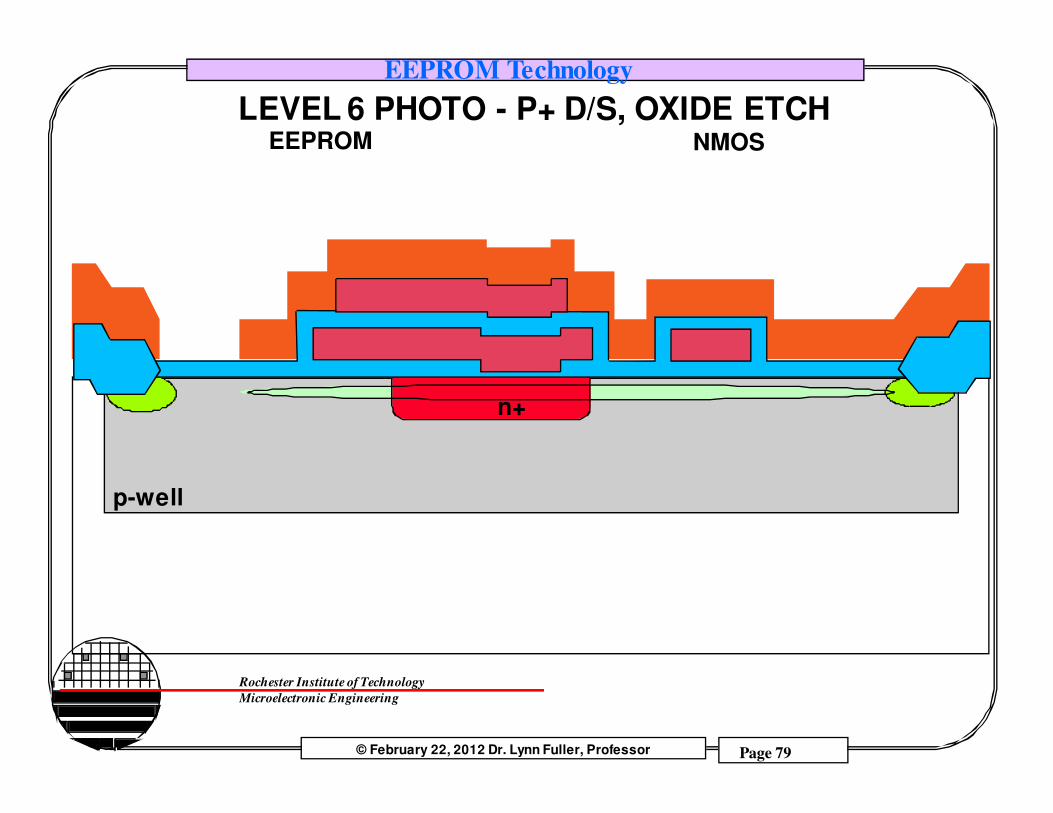
EEPROM NMOS
p-well
n+
LEVEL 6 PHOTO - P+ D/S, OXIDE ETCH

© February 22, 2012 Dr. Lynn Fuller, Professor
Rochester Institute of Technology
Microelectronic Engineering
EEPROM Technology
Page 80
ION IMPLANT P+ D/S
4e15, 120 KeV, BF2 into bare silicon
EEPROM NMOS
p-well
n+
4e15, 120 KeV, BF2 into bare silicon
11B, keV, e
© February 22, 2012 Dr. Lynn Fuller, Professor
Rochester Institute of Technology
Microelectronic Engineering
EEPROM Technology
Page 81
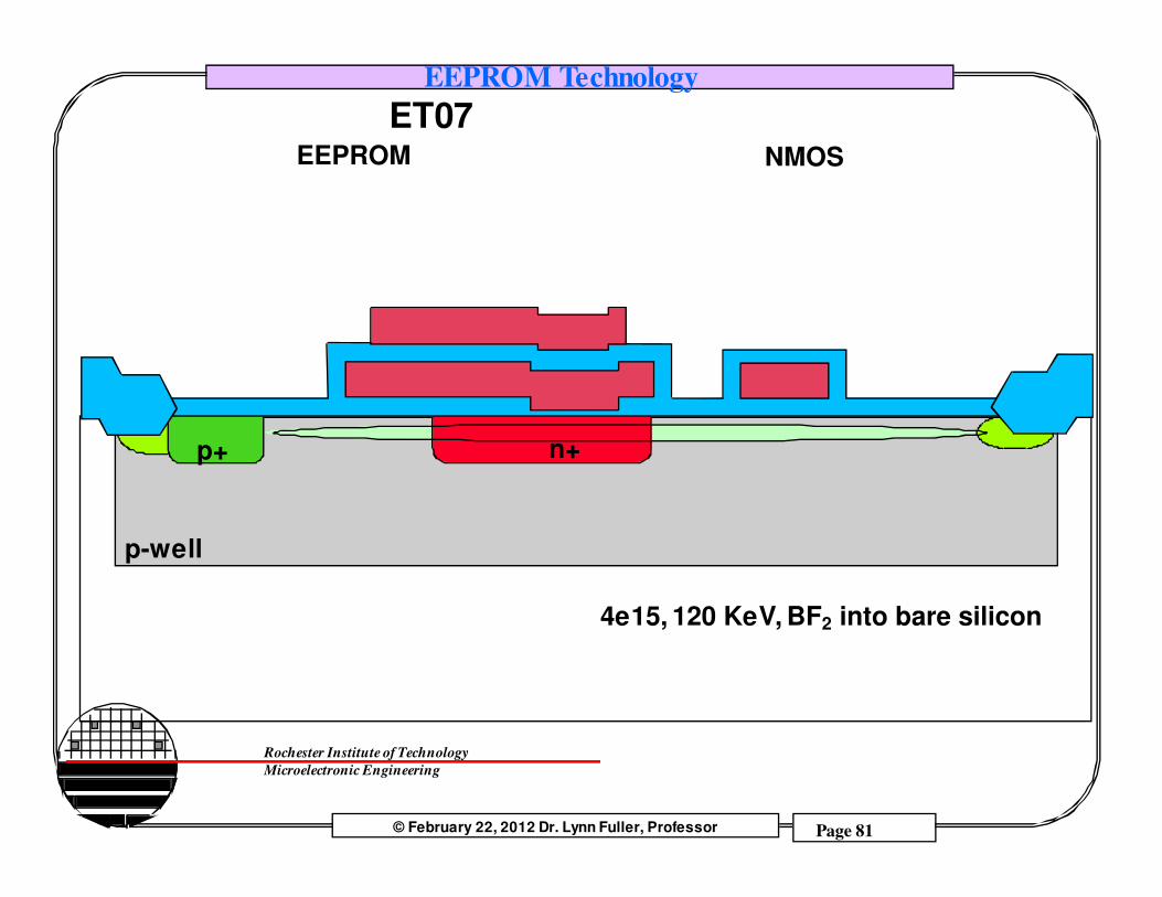
ET07
4e15, 120 KeV, BF2 into bare silicon
EEPROM NMOS
p-well
n+p+
4e15, 120 KeV, BF2 into bare silicon

© February 22, 2012 Dr. Lynn Fuller, Professor
Rochester Institute of Technology
Microelectronic Engineering
EEPROM Technology
Page 82
LEVEL 7 PHOTO - N+ D/S
4e15, 120 KeV, BF2 into bare silicon
EEPROM NMOS
p-well
n+p+

© February 22, 2012 Dr. Lynn Fuller, Professor
Rochester Institute of Technology
Microelectronic Engineering
EEPROM Technology
Page 83
EEPROM NMOS
p-well
n+p+
ION IMPLANT N+ D/S
4e15, 100KeV, P31 thru gate Oxide
11B, 60 keV, 1.2e12
© February 22, 2012 Dr. Lynn Fuller, Professor
Rochester Institute of Technology
Microelectronic Engineering
EEPROM Technology
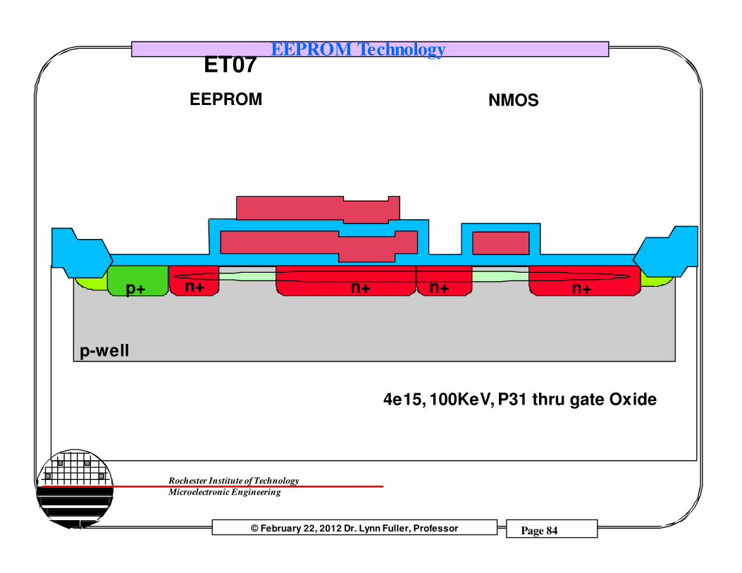
Page 84
EEPROM NMOS
p-well
n+ n+ n+p+ n+
ET07
4e15, 100KeV, P31 thru gate Oxide
© February 22, 2012 Dr. Lynn Fuller, Professor
Rochester Institute of Technology
Microelectronic Engineering
EEPROM Technology
Page 85
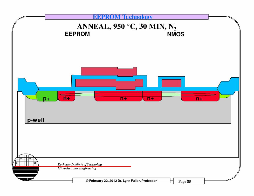
ANNEAL, 950 °C, 30 MIN, N2EEPROM NMOS
p-well
n+ n+ n+p+ n+
© February 22, 2012 Dr. Lynn Fuller, Professor
Rochester Institute of Technology
Microelectronic Engineering
EEPROM Technology
Page 86
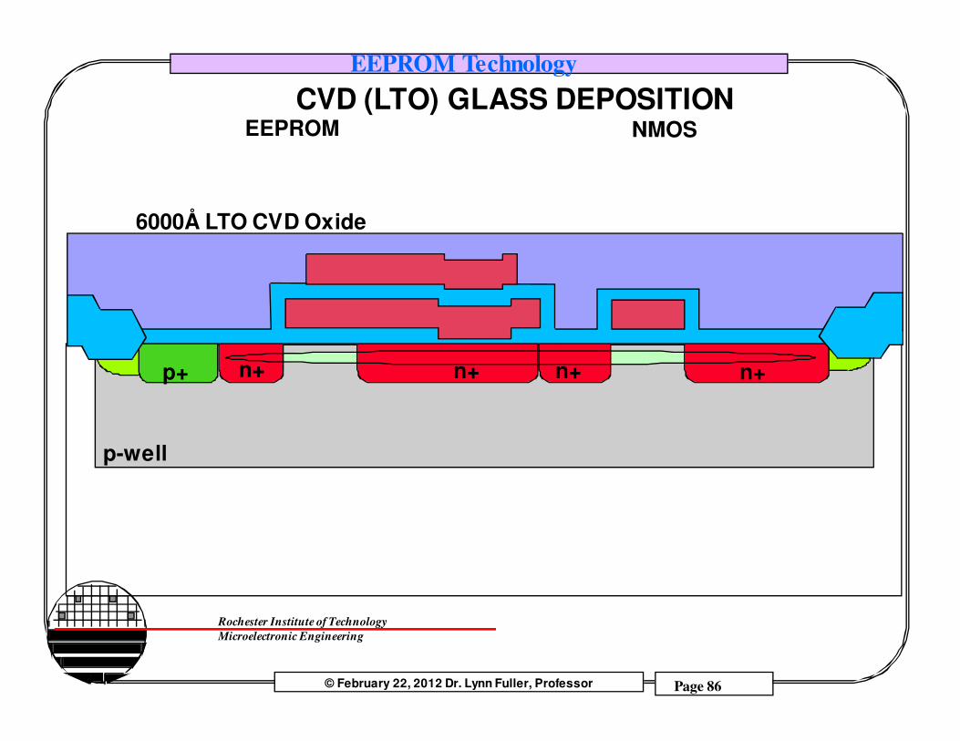
EEPROM NMOS
p-well
n+ n+ n+p+ n+
CVD (LTO) GLASS DEPOSITION
6000Å LTO CVD Oxide

© February 22, 2012 Dr. Lynn Fuller, Professor
Rochester Institute of Technology
Microelectronic Engineering
EEPROM Technology
Page 87
LEVEL 8 PHOTO - CONTACT CUT
Etch in BHF 7min
EEPROM NMOS
p-well
n+ n+ n+p+ n+

© February 22, 2012 Dr. Lynn Fuller, Professor
Rochester Institute of Technology
Microelectronic Engineering
EEPROM Technology
Page 88
EEPROM NMOS
p-well
n+ n+ n+p+ n+
CONTACT CUT ETCH

© February 22, 2012 Dr. Lynn Fuller, Professor
Rochester Institute of Technology
Microelectronic Engineering
EEPROM Technology
Page 89
STRIP RESISTEEPROM NMOS
p-well
n+ n+ n+p+ n+
© February 22, 2012 Dr. Lynn Fuller, Professor
Rochester Institute of Technology
Microelectronic Engineering
EEPROM Technology
Page 90
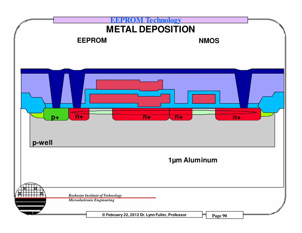
EEPROM NMOS
p-well
n+ n+ n+p+ n+
METAL DEPOSITION
1µm Aluminum
© February 22, 2012 Dr. Lynn Fuller, Professor
Rochester Institute of Technology
Microelectronic Engineering
EEPROM Technology
Page 91
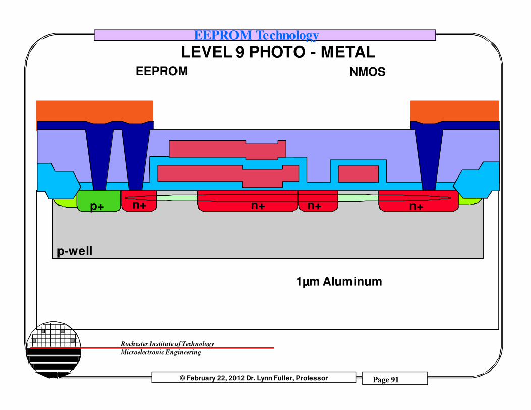
EEPROM NMOS
p-well
n+ n+ n+p+ n+
1µm Aluminum
LEVEL 9 PHOTO - METAL

© February 22, 2012 Dr. Lynn Fuller, Professor
Rochester Institute of Technology
Microelectronic Engineering
EEPROM Technology
Page 92
ETCH METAL AND STRIP RESISTEEPROM NMOS
p-well
n+ n+ n+p+ n+
© February 22, 2012 Dr. Lynn Fuller, Professor
Rochester Institute of Technology
Microelectronic Engineering
EEPROM Technology
Page 93
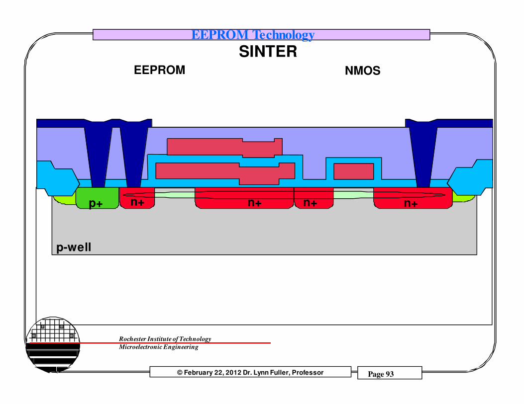
SINTEREEPROM NMOS
p-well
n+ n+ n+p+ n+

© February 22, 2012 Dr. Lynn Fuller, Professor
Rochester Institute of Technology
Microelectronic Engineering
EEPROM Technology
Page 94
EEPROMEEPROM
NMOS
Vt adj blanket and nmose , 60 KeV B11, 1000Å Kooi
field Vt adj 8e13B11, 100KeV Bare
1 µm Aluminum
p+ D/S 4e15, 120 KeVBF2 into bare silicon
n+ D/S 4e15, 100KeVP31 thru gate Oxide
p-well 4e12, 50 keV, B11, 1123 C, 20 hr
n+ D/S 4e15, 100KeVP31 thru gate Oxide
n+ n+ n+p+ n+

© February 22, 2012 Dr. Lynn Fuller, Professor
Rochester Institute of Technology
Microelectronic Engineering
EEPROM Technology
Page 95
© February 22, 2012 Dr. Lynn Fuller, Professor
Rochester Institute of Technology
Microelectronic Engineering
EEPROM Technology
Page 96

© February 22, 2012 Dr. Lynn Fuller, Professor
Rochester Institute of Technology
Microelectronic Engineering
EEPROM Technology
Page 97