cmos processing technology - national tsing hua · pdf file · 2016-09-04cmos...
TRANSCRIPT
VLSI Design
2-
Chih-Cheng Hsieh
CMOS Processing Technology
CHAPTER 2
VLSI Design
2-
Chih-Cheng Hsieh
Outline 2
1. CMOS Technologies
2. Layout Design Rules
3. CMOS Process Enhancements
4. Technology-related CAD Issues
5. Manufacturing Issues

VLSI Design
2-
Chih-Cheng Hsieh
CMOS Technologies 3
• n-well Process : p-substrate
• p-well Process : n-substrate
• Twin-well Process – Optimized for each transistor type
• Triple-well Process (deep n-well) – Good isolation between analog & digital blocks
• BiCMOS Process (SiGe)
• Silicon-on-insulator (SOI) Process
VLSI Design
2-
Chih-Cheng Hsieh
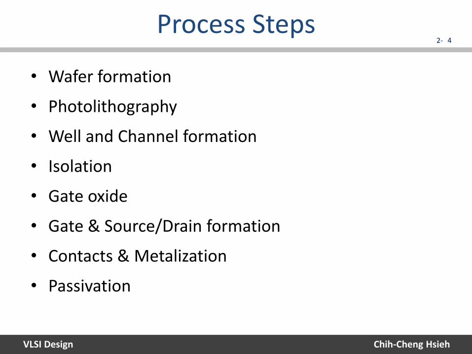
Process Steps 4
• Wafer formation
• Photolithography
• Well and Channel formation
• Isolation
• Gate oxide
• Gate & Source/Drain formation
• Contacts & Metalization
• Passivation

VLSI Design
2-
Chih-Cheng Hsieh
Photolithography 5
• Resolution enhancement techniques
– Optical proximity correction (OPC) : local distortion, Phase shift masks (PSM): light diffraction, Off-axis illumination (OAI): contrast enhancement of repetitive pattern.
• Greek: Photo(light)+lithos(stone)+graphe(picture) – Carving pictures in stone using light
http://nano.nchc.org.tw/dictionary/Optical_Lithography.html
VLSI Design
2-
Chih-Cheng Hsieh
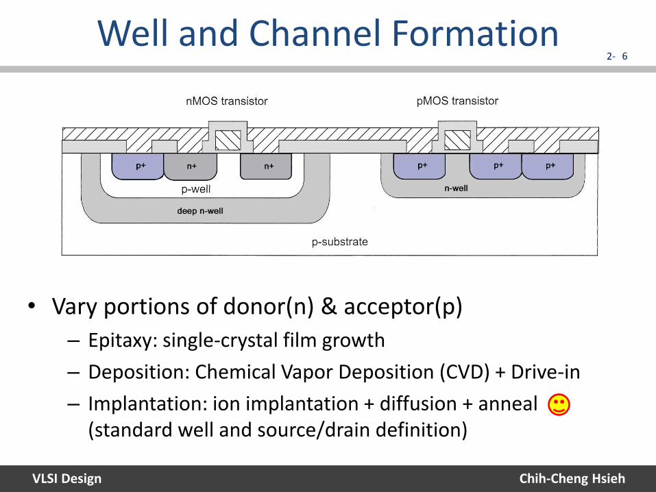
Well and Channel Formation 6
• Vary portions of donor(n) & acceptor(p)
– Epitaxy: single-crystal film growth
– Deposition: Chemical Vapor Deposition (CVD) + Drive-in
– Implantation: ion implantation + diffusion + anneal (standard well and source/drain definition)
VLSI Design
2-
Chih-Cheng Hsieh
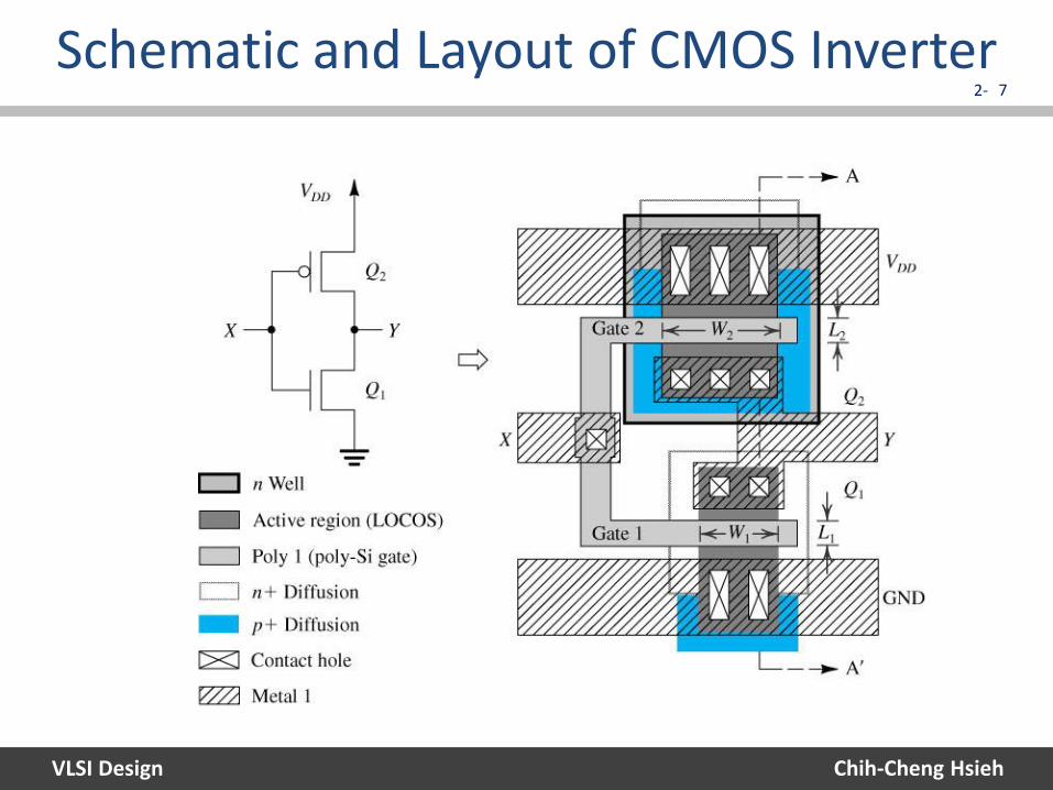
Schematic and Layout of CMOS Inverter 7

VLSI Design
2-
Chih-Cheng Hsieh
Cross Section of CMOS Inverter 8

VLSI Design
2-
Chih-Cheng Hsieh
Photomasks of n-well CMOS Inverter 9

VLSI Design
2-
Chih-Cheng Hsieh
n-Well CMOS Process - 1 10
(a) Define n-well diffusion (mask #1)
(b) Define active regions thin oxide (mask #2)
(d) Polysilicon gate (mask #3) (c) LOCOS oxidation field oxide
VLSI Design
2-
Chih-Cheng Hsieh
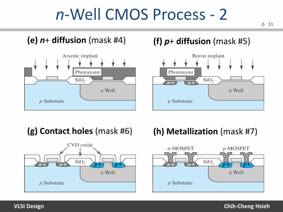
n-Well CMOS Process - 2 11
(h) Metallization (mask #7) (g) Contact holes (mask #6)
(e) n+ diffusion (mask #4) (f) p+ diffusion (mask #5)
VLSI Design
2-
Chih-Cheng Hsieh
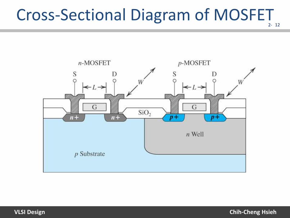
Cross-Sectional Diagram of MOSFET 12
VLSI Design
2-
Chih-Cheng Hsieh
Silicon Dioxide (SiO2) 13
• Wet oxidation – Oxidizing atmosphere contains water vapor, Temp:
900~1000oC, quick for thick oxides.
• Dry oxidation – Oxidizing atmosphere is pure oxygen, Temp: ~1200oC,
highly controlled thin oxides.
• Atomic layer deposition – Thin chemical layer deposition for various requirement
(SiO2, metal, dielectrics)
VLSI Design
2-
Chih-Cheng Hsieh
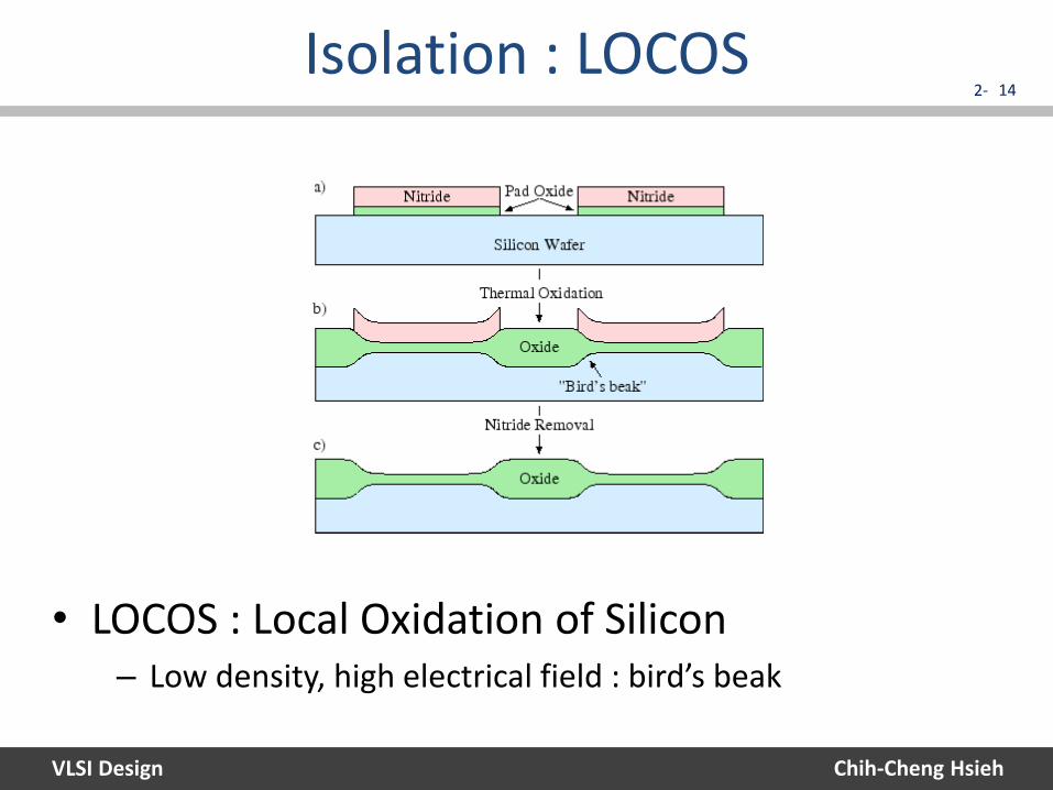
Isolation : LOCOS 14
• LOCOS : Local Oxidation of Silicon – Low density, high electrical field : bird’s beak
VLSI Design
2-
Chih-Cheng Hsieh
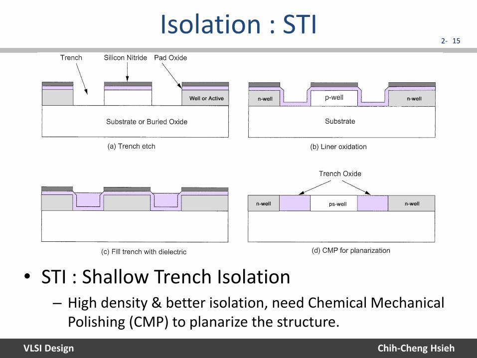
Isolation : STI 15
• STI : Shallow Trench Isolation – High density & better isolation, need Chemical Mechanical
Polishing (CMP) to planarize the structure.

VLSI Design
2-
Chih-Cheng Hsieh
Gate Oxide 16
• Shorter gate L thinner gate oxide
• EOT : Effective Oxide Thickness – Use stack gate
structure with high-K dielectric to decrease EOT.
• Dual gate oxide for core and I/O.

VLSI Design
2-
Chih-Cheng Hsieh
Gate & Source/Drain Formation 17
• Self-aligned poly-silicon (poly) gate
• Lightly doped drain (LDD) structure

VLSI Design
2-
Chih-Cheng Hsieh
LDD & Salicide 18
• LDD – Reduce electrical field of drain
junction & hot-electron damage
– High sheet resistance
• Salicide : self-aligned silicide – Refractory metal to reduce the
interconnection resistance of gate, source/drain.
• CMP : – Structure planarization for further
stack process.
VLSI Design
2-
Chih-Cheng Hsieh
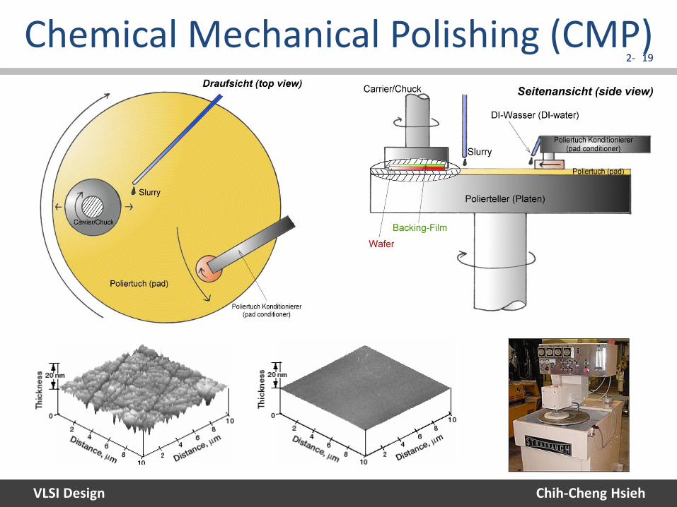
Chemical Mechanical Polishing (CMP) 19

VLSI Design
2-
Chih-Cheng Hsieh
Contacts & Metallization 20
• Contact – Metal Poly, Metal Diffusion
• VIA – Metal Metal
• CMP : – Structure planarization for further stack process.
VLSI Design
2-
Chih-Cheng Hsieh
Outline 21
1. CMOS Technologies
2. Layout Design Rules
3. CMOS Process Enhancements
4. Technology-related CAD Issues
5. Manufacturing Issues

VLSI Design
2-
Chih-Cheng Hsieh
Layout Design Rule 22
• Design rule: geometric constraint and tolerance for high probability of correct fabrication.
– Feature size, separations and overlaps.
• Well rule : isolation
• Transistor rule : channel quality
– Poly, active region, n+/p+ implant.
• Contact : single size for precisely process control
• Metal & Via rule: productivity & conductivity
– Top metal with loser size, space and via rules.
VLSI Design
2-
Chih-Cheng Hsieh
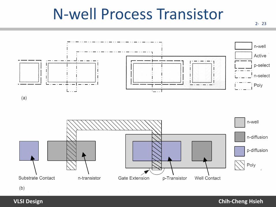
N-well Process Transistor 23

VLSI Design
2-
Chih-Cheng Hsieh
Design Rule 24
VLSI Design
2-
Chih-Cheng Hsieh
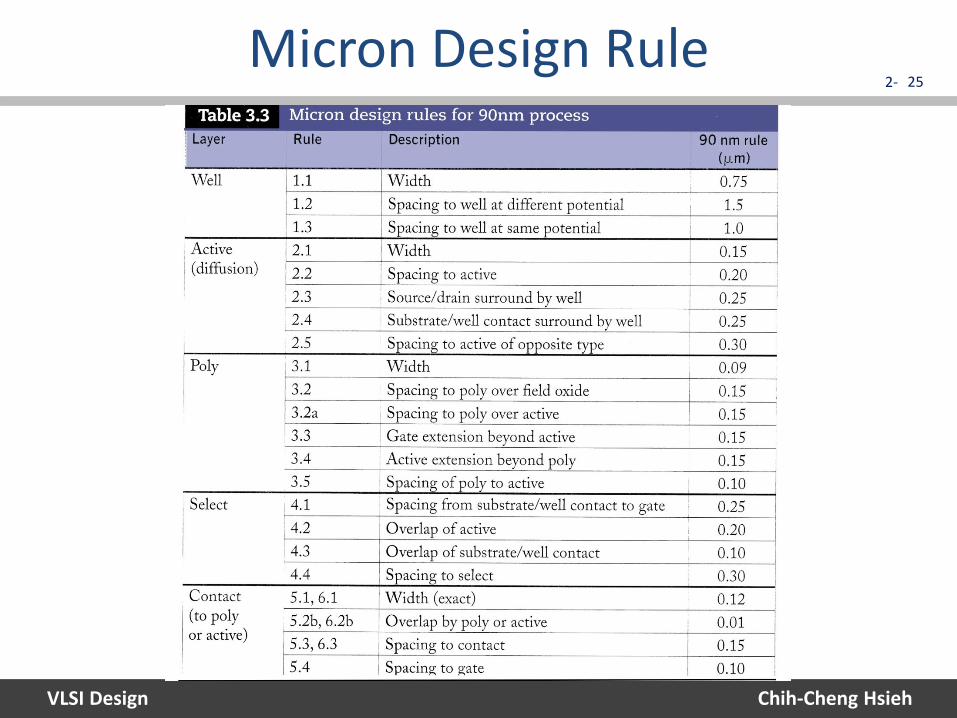
Micron Design Rule 25
VLSI Design
2-
Chih-Cheng Hsieh
Outline 26
1. CMOS Technologies
2. Layout Design Rules
3. CMOS Process Enhancements
4. Technology-related CAD Issues
5. Manufacturing Issues
VLSI Design
2-
Chih-Cheng Hsieh
CMOS Process Enhancement 27
• Multiple threshold voltage & oxide thickness
– Low core voltage for low power
– High I/O voltage for interface compatibility
• Silicon on Insulator : higher speed
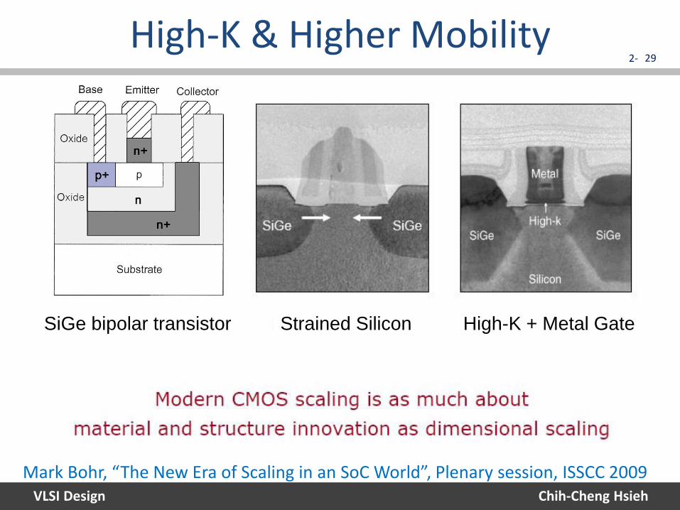
• High-K gate dielectrics : thinner EOT
• Higher mobility : SiGe BJT, strained silicon
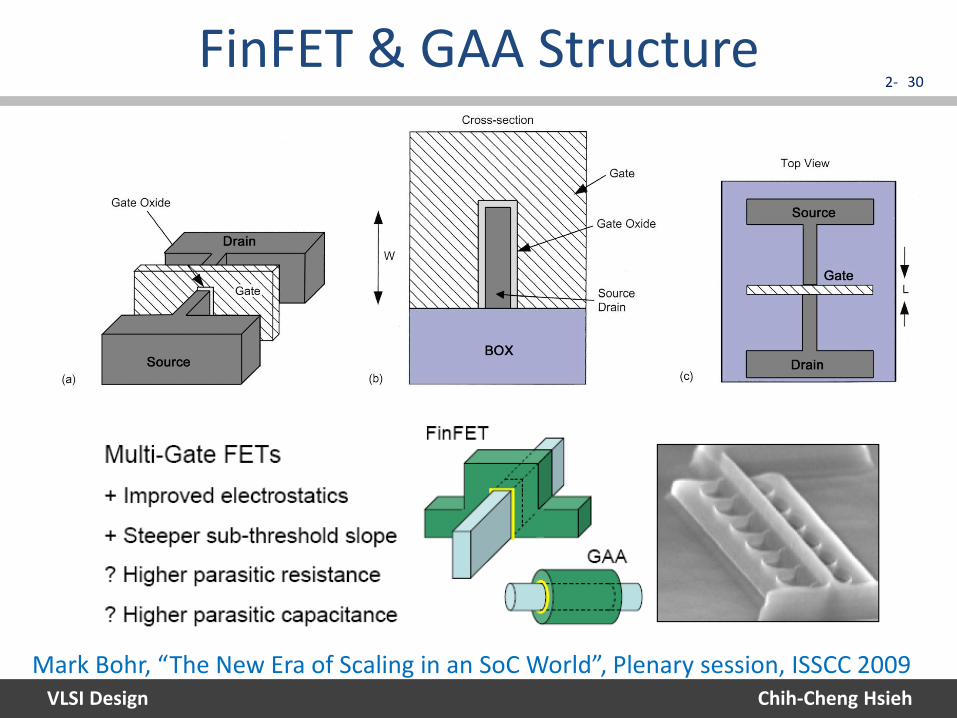
• Low-leakage transistor : finFET, gate-all-around (GAA) FET
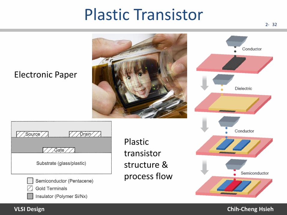
• Plastic Transistors : flexible electronic paper
• High-voltage transistor : LCD driver, power electronics
• Copper interconnection : high conductivity
• Low-K dielectrics : low wire capacitance
VLSI Design
2-
Chih-Cheng Hsieh
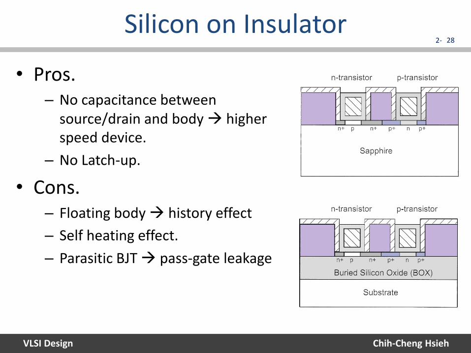
Silicon on Insulator 28
• Pros. – No capacitance between
source/drain and body higher speed device.
– No Latch-up.
• Cons. – Floating body history effect
– Self heating effect.
– Parasitic BJT pass-gate leakage
VLSI Design
2-
Chih-Cheng Hsieh
High-K & Higher Mobility 29
Mark Bohr, “The New Era of Scaling in an SoC World”, Plenary session, ISSCC 2009
SiGe bipolar transistor Strained Silicon High-K + Metal Gate
VLSI Design
2-
Chih-Cheng Hsieh
FinFET & GAA Structure 30
Mark Bohr, “The New Era of Scaling in an SoC World”, Plenary session, ISSCC 2009

VLSI Design
2-
Chih-Cheng Hsieh
Transistor Scaling 31
http://isscc.org/media/2012/plenary/David_Perlmutter/SilverlightLoader.html
VLSI Design
2-
Chih-Cheng Hsieh
Plastic Transistor 32
Electronic Paper
Plastic transistor structure & process flow

VLSI Design
2-
Chih-Cheng Hsieh
Copper Interconnect 33
• Copper atoms diffuse into the silicon and dielectrics, destroying transistors
– Barrier layers are necessary
• The processing required to etch copper wires is tricky.
• Copper oxide forms readily and interferes with good contacts.
• Care has to be taken not to introduce copper into the environment as a pollutant

VLSI Design
2-
Chih-Cheng Hsieh
Copper Damascene Process 34
• Pros. : High conductivity
• Cons. :Complex process
VLSI Design
2-
Chih-Cheng Hsieh
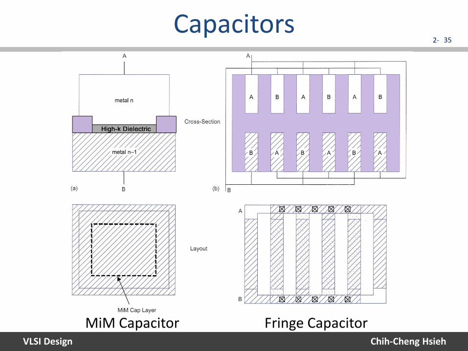
Capacitors 35
MiM Capacitor Fringe Capacitor
VLSI Design
2-
Chih-Cheng Hsieh
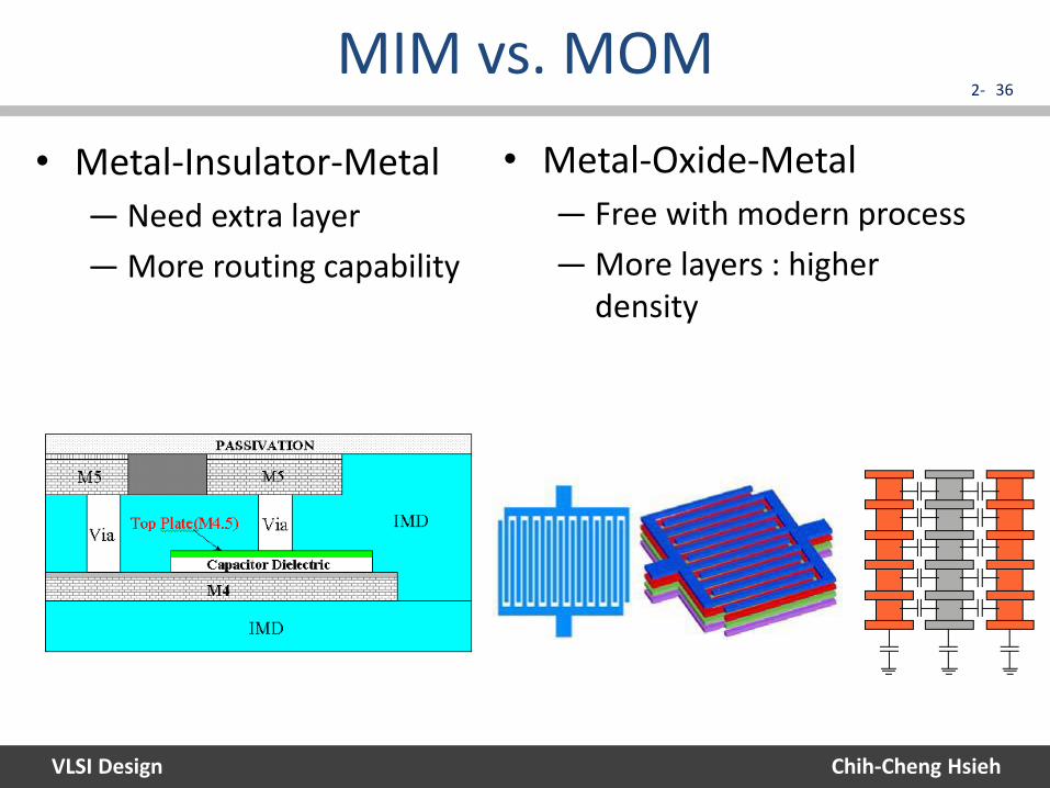
MIM vs. MOM 36
• Metal-Insulator-Metal
— Need extra layer
— More routing capability
• Metal-Oxide-Metal
— Free with modern process
— More layers : higher density

VLSI Design
2-
Chih-Cheng Hsieh
Resistor & Conductor 37
Non-silicide high-resistivity Poly resistor
Planar spiral Inductor
VLSI Design
2-
Chih-Cheng Hsieh
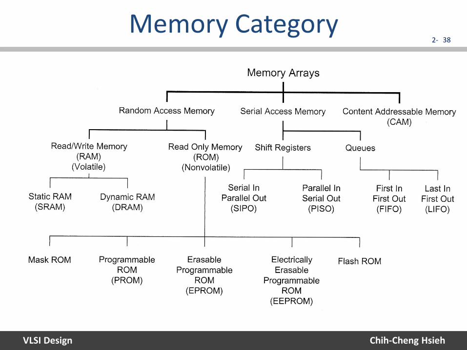
Memory Category 38

VLSI Design
2-
Chih-Cheng Hsieh
Non-Volatile Memory (NVM) 39
• Mask-programmed ROM (Read-Only Memory) – NOT programmable after manufacture.
• One-Time Programmable (OTP) memory – Fuse constructed programming flow
• EPROM: Electrically Programmable ROM – Electrical Programming, UV Erase
• EEPROM: Electrically Erasable PROM – Electrical Programming & Erase, Byte-level programming.
• Flash – Block-level programming, faster & cheaper than EEPROM
VLSI Design
2-
Chih-Cheng Hsieh
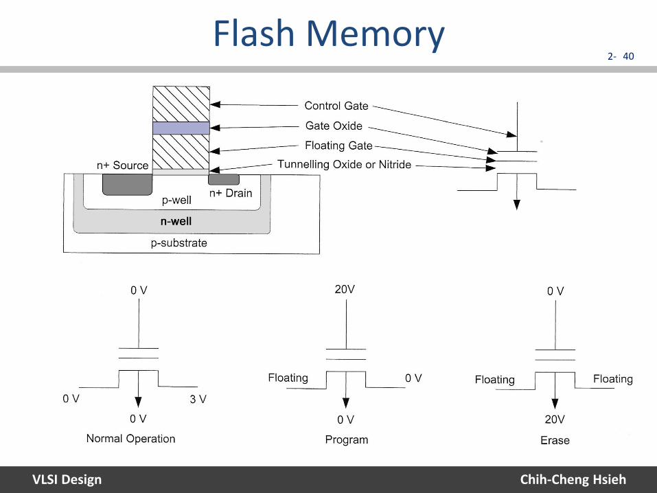
Flash Memory 40
VLSI Design
2-
Chih-Cheng Hsieh
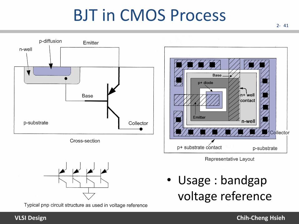
BJT in CMOS Process 41
• Usage : bandgap voltage reference
VLSI Design
2-
Chih-Cheng Hsieh
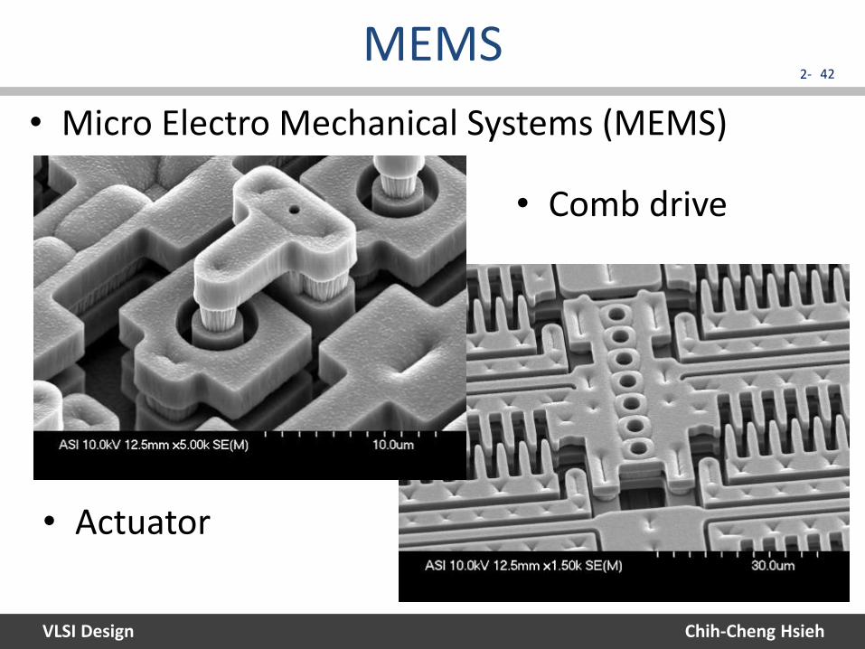
MEMS 42
• Micro Electro Mechanical Systems (MEMS)
• Actuator
• Comb drive

VLSI Design
2-
Chih-Cheng Hsieh
Carbon Nanotube (CNT) Transistor 43
• Smaller channel length
• Higher speed
• Lower power
• Better electrical performance than Si but complex process
IBM CNTFET

VLSI Design
2-
Chih-Cheng Hsieh
Outline 44
1. CMOS Technologies
2. Layout Design Rules
3. CMOS Process Enhancements
4. Technology-related CAD Issues
5. Manufacturing Issues
VLSI Design
2-
Chih-Cheng Hsieh
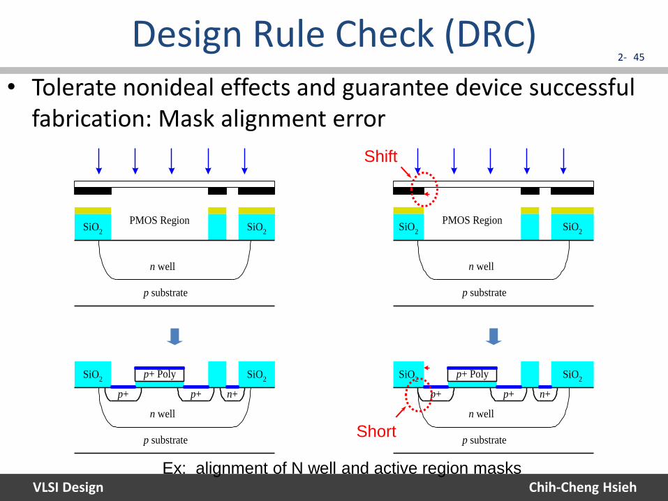
Design Rule Check (DRC) 45
• Tolerate nonideal effects and guarantee device successful fabrication: Mask alignment error
SiO2
SiO2
p substrate
n well
PMOS Region
SiO2
SiO2
p substrate
n well
p+ Poly
p+ p+ n+
SiO2
SiO2
p substrate
n well
PMOS Region
SiO2
SiO2
p substrate
n well
p+ Poly
p+ p+ n+
Short
Shift
Ex: alignment of N well and active region masks

VLSI Design
2-
Chih-Cheng Hsieh
Design Rule Check (DRC) 46
• Exposure and etching variation – Ex: different contact windows different contact resistance
SiO2
SiO2
P substrate
N well
P+ P+ N+
Contact widows
Minimum
width
Minimum
spacing
Poly overlap
Poly-contact
spacing
Contact overlap Poly-diff.
spacing
Contact
overlap
Resolution Alignment
• Two types of design rules

VLSI Design
2-
Chih-Cheng Hsieh
Design Rule Check (DRC) 47
• Minimum channel width
– CO.W.1 + 2 CO.E.1
• Minimize S/D diffusion width (xd)
– CO.W.1 + CO.E.1 + CO.C.1
xd
xd

VLSI Design
2-
Chih-Cheng Hsieh
Layout v.s. Schematic (LVS) 48
• Guarantee the layout is the same as the simulated netlist
– Check device parameters, interconnections and i/o ports.
Model name
Channel width
Channel length
VDD
VO VI
GND
VDD
GND
VI VO
VLSI Design
2-
Chih-Cheng Hsieh
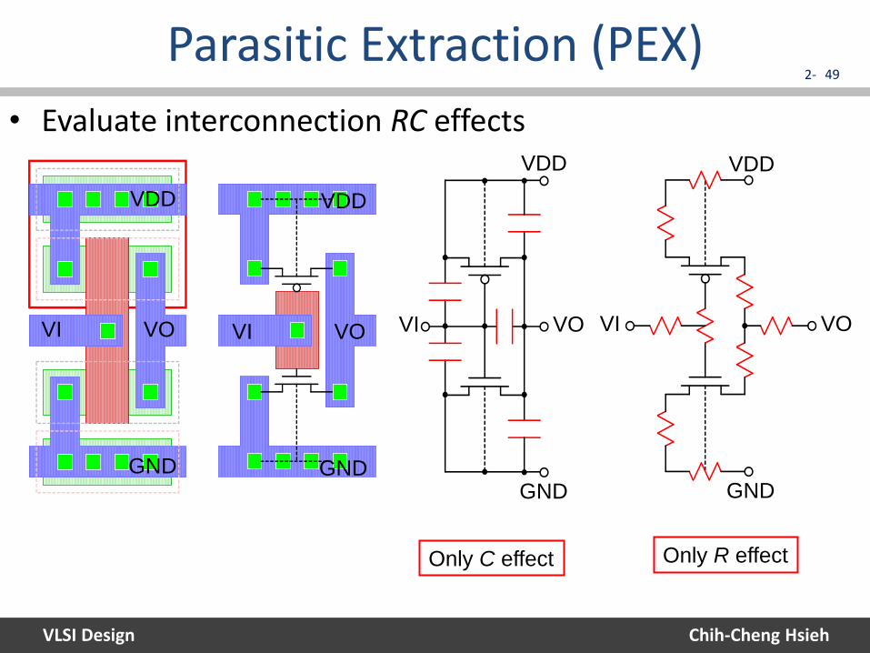
Parasitic Extraction (PEX) 49
• Evaluate interconnection RC effects
VDD
GND
VI VO
VDD
GND
VI VO
VDD
GND
VI VO
Only C effect Only R effect
VDD
GND
VI VO
VLSI Design
2-
Chih-Cheng Hsieh
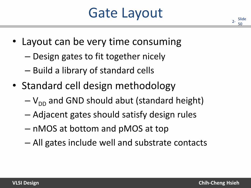
Gate Layout Slide 50
• Layout can be very time consuming
– Design gates to fit together nicely
– Build a library of standard cells
• Standard cell design methodology
– VDD and GND should abut (standard height)
– Adjacent gates should satisfy design rules
– nMOS at bottom and pMOS at top
– All gates include well and substrate contacts
VLSI Design
2-
Chih-Cheng Hsieh
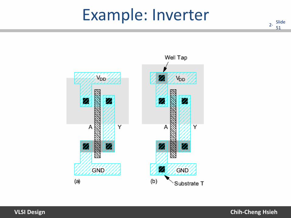
Example: Inverter Slide 51

VLSI Design
2-
Chih-Cheng Hsieh
Simplified λ-Based Design Rules 52

VLSI Design
2-
Chih-Cheng Hsieh
Example: NAND3 53
• Horizontal N-diffusion and p-diffusion strips
• Vertical polysilicon gates
• Metal1 VDD rail at top
• Metal1 GND rail at bottom
• 32 l by 40 l

VLSI Design
2-
Chih-Cheng Hsieh
Stick Diagrams 54
• Stick diagrams help plan layout quickly
– Need not be to scale
– Draw with color pencils or dry-erase markers

VLSI Design
2-
Chih-Cheng Hsieh
Wiring Tracks 55
• A wiring track is the space required for a wire
– 4 l width, 4 l spacing from neighbor = 8 l pitch
• Transistors also consume one wiring track
VLSI Design
2-
Chih-Cheng Hsieh
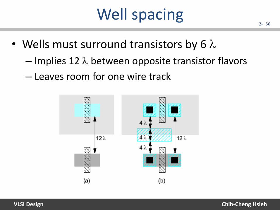
Well spacing 56
• Wells must surround transistors by 6 l
– Implies 12 l between opposite transistor flavors
– Leaves room for one wire track
VLSI Design
2-
Chih-Cheng Hsieh
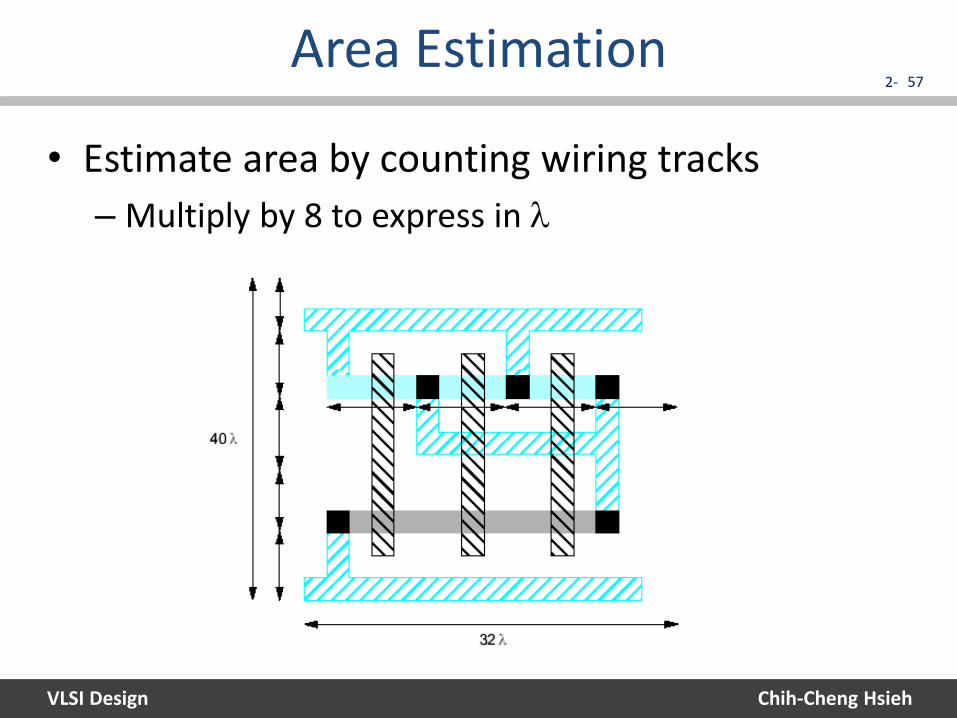
Area Estimation 57
• Estimate area by counting wiring tracks
– Multiply by 8 to express in l
VLSI Design
2-
Chih-Cheng Hsieh
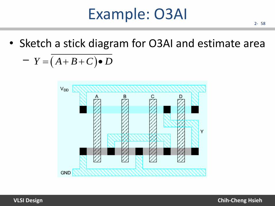
Example: O3AI 58
• Sketch a stick diagram for O3AI and estimate area
– Y A B C D
VLSI Design
2-
Chih-Cheng Hsieh
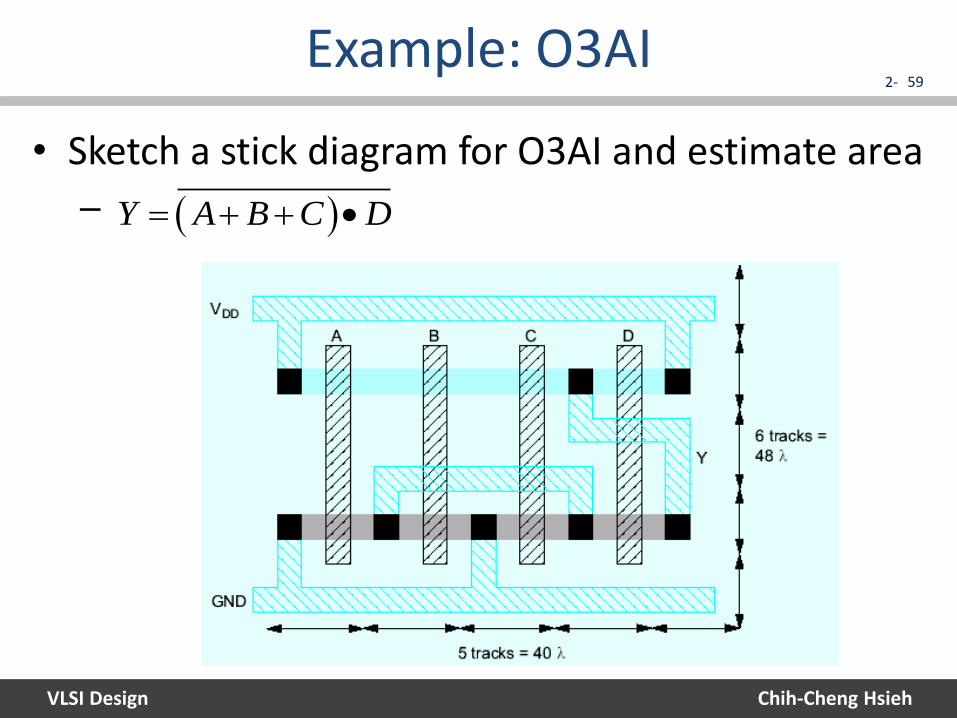
Example: O3AI 59
• Sketch a stick diagram for O3AI and estimate area
– Y A B C D
VLSI Design
2-
Chih-Cheng Hsieh
Outline 60
1. CMOS Technologies
2. Layout Design Rules
3. CMOS Process Enhancements
4. Technology-related CAD Issues
5. Manufacturing Issues

VLSI Design
2-
Chih-Cheng Hsieh
Antenna Rules 61
Maximum area of metal connected to gate without discharge element

VLSI Design
2-
Chih-Cheng Hsieh
Layer Density Rule 62
• CMP & Uniform etch process requirement : Planarization
• Solution : Pattern Fill (by CAD)
Reference: http://www.edadesignline.com/howto/198100760;jsessionid=EWGKEU5KZKDCVQE1GHPSKH4ATMY32JVN?pgno=2