coarse-grained reconfigurable array architecturesbrdsutte/research/... · bjorn de sutter, praveen...
TRANSCRIPT

Coarse-Grained Reconfigurable ArrayArchitectures
Bjorn De Sutter, Praveen Raghavan, Andy Lambrechts
Abstract Coarse-Grained Reconfigurable Array (CGRA) architecturesacceleratethe same inner loops that benefit from the high ILP support in VLIW architectures.By executing non-loop code on other cores, however, CGRAs can focus on suchloops to execute them more efficiently. This chapter discusses the basic principlesof CGRAs, and the wide range of design options available to a CGRA designer,covering a large number of existing CGRA designs. The impactof different optionson flexibility, performance, and power-efficiency is discussed, as well as the needfor compiler support. The ADRES CGRA design template is studied in more detailas a use case to illustrate the need for design space exploration, for compiler supportand for the manual fine-tuning of source code.
1 Application Domain of Coarse-Grained Reconfigurable Arrays
Many embedded applications require high throughput, meaning that a large numberof computations needs to be performed every second. At the same time, the powerconsumption of battery-operated devices needs to be minimized to increase theirautonomy. In general, the performance obtained on a programmable processor for acertain application can be defined as the reciprocal of the application execution time.Considering that most programs consist of a number of consecutive phasesP= [1, p]with different characteristics, performance can be definedin terms of the operatingfrequenciesfp, the instructions executed per cycleIPCp and the instruction countsICp of each phase, and in terms of the time overhead involved in switching betweenthe phasestp→p+1 as follows:
Bjorn De SutterGhent University, Sint-Pietersnieuwstraat 41, 9000 Gent,Belgium and Vrije Universiteit Brussel,Pleinlaan 2, 1050 Brussel, Belgium, e-mail: [email protected]
Praveen Raghavan, Andy LambrechtsIMEC, Kapeldreef 75, 3001 Heverlee, Belgium e-mail:{ragha,lambreca}@imec.be
1

2 Bjorn De Sutter, Praveen Raghavan, Andy Lambrechts
1performance
= execution time= ∑p∈P
ICp
IPCp∗ fp+ tp→p+1. (1)
The operating frequenciesfp cannot be increased infinitely because of power-efficiency reasons. Alternatively, a designer can increasethe performance by de-signing or selecting a system that can execute code at higherIPCs. In a power-efficient architecture, a high IPC is reached for the most important phasesl ∈ L ⊂P,while limiting their instruction countICl and reaching a sufficiently high, but stillpower-efficient frequencyfl . Furthermore, the time overheadtp→p+1 as well as thecorresponding energy overhead of switching between the execution modes of con-secutive phases should be minimized if such switching happens frequently. Note thatsuch switching only happens on hardware that supports multiple execution modesin support of phases with different characteristics.
Course-Grained Reconfigurable Array (CGRA) accelerators aim for these goalsfor the inner loops found in many digital signal processing (DSP) domains, includ-ing multimedia and Software-Defined Radio (SDR) applications. Such applicationshave traditionally employed Very Long Instruction Word (VLIW) architectures suchas the TriMedia 3270 [60] and the TI C64 [58], Application-Specific Integrated Cir-cuits (ASICs), and Application-Specific Instruction Processors (ASIPs). To a largedegree, the reasons for running these applications on VLIW processors also ap-ply for CGRAs. First of all, a large fraction of the computation time is spent inmanifest nested loops that perform computations on arrays of data and that can,possibly through compiler transformations, provide a lot of Instruction-Level Par-allelism (ILP). Secondly, most of those inner loops are relatively simple. When theloops include conditional statements, this can be implement by means of predi-cation [36] instead of with complex control flow. Furthermore, none or very fewloops contain multiple exits or continuation points in the form of, e.g.,break orcontinue statements as in the C-language. Moreover, after inlining the loops arefree of function calls. Finally, the loops are not regular orhomogeneous enoughto benefit from vector computing, like on the EVP [59] or on Ardbeg [62]. Whenthere is enough regularity and Data-Level Parallelism (DLP) in the loops of an ap-plication, vector computing can typically exploit it more efficiently than what canbe achieved by converting the DLP into ILP and exploiting that on a CGRA. Soin short, CGRAs (with limited DLP support) are ideally suited for applications ofwhich time-consuming parts have manifest behavior, large amounts of ILP and lim-ited amounts of DLP.
In the remainder of this chapter, Section 2 presents the fundamental propertiesof CGRAs. Section 3 gives an overview of the design options for CGRAs. Thisoverview help designers in evaluating whether or not CGRAs are suited for theirapplications and their design requirements, and if so, which CGRA designs are mostsuited. After the overview, Section 4 presents a case study on the ADRES CGRAarchitecture. This study serves two purposes. First, it illustrates the extent to whichsource code needs to be tuned to map well onto CGRA architectures. As we willshow, this is an important aspect of using CGRAs, even when good compiler sup-port is available and when a very flexible CGRA is targeted, i.e., one that puts very

Coarse-Grained Reconfigurable Array Architectures 3
RF 0
IS 0 IS 1 IS 2 IS 3
RF 1
IS 4 IS 5 IS 6 IS 7
Fig. 1 An example clustered VLIW architecture with two RFs and eight ISs. Solid directed edgesdenote physical connections. Black and white small boxes denote input and output ports, respec-tively. There is a one-to-one mapping between input and output ports and physical connections.
few restrictions on the loop bodies that it can accelerate. Secondly, our use case il-lustrates how Design Space Exploration (DSE) is necessary to instantiate optimizeddesigns from parameterizable and customizable architecture templates such as theADRES architecture template. Some conclusions are drawn inSection 5.
2 CGRA Basics
CGRAs focus on the efficient execution of the type of loops discussed in the previ-ous section. By neglecting non-loop code or outer-loop codethat is assumed to beexecuted on other cores, CGRAs can take the VLIW principles for exploiting ILP inloops a step further to consume less energy and deliver higher performance, withoutcompromising on available compiler support. Figures 1 and 2illustrate this.
Higher performance for high-ILP loops is obtained through two main fea-tures that separate CGRA architectures from VLIW architectures. First, CGRAarchitectures typically provide more Issue Slots (ISs) than typical VLIWs do.In the CGRA literature some other commonly used terms to denote CGRA ISsare Arithmetic-Logic Units (ALUs), Functional Units (FUs), or Processing El-ements (PEs). Conceptually, these terms all denote the same: logic on whichan instruction can be executed, typically one per cycle. Forexample, a typicalADRES [5, 6, 7, 15, 37, 39, 40, 41] CGRA consists of 16 ISs, whereas the TI C64features 8 slots, and the NXP TriMedia features only 5 slots.The higher numberof ISs directly allows to reach higher IPCs, and hence higherperformance, as indi-cated by Equation (1). To support these higher IPCs, the bandwidth to memory isincreased by having more load/store ISs than on a typical VLIW, and special mem-ory hierarchies as found on ASIPs, ASICs, and other DSPs. These include FIFOs,stream buffers, scratch-pad memories, etc. Secondly, CGRAarchitectures typicallyprovide a number of direct connections between the ISs that allow data to “flow”from one IS to another without needing to pass data through a Register File (RF).As a result, less register copy operations need to be executed in the ISs, which re-duces the IC term in Equation (1) and frees ISs for more usefulcomputations.
Higher energy efficiency is obtained through several features. Because of the di-rect connections between ISs, less data needs to be transferred into and out of RFs.This saves considerable energy. Also, because the ISs are arranged into a 2D matrix,

4 Bjorn De Sutter, Praveen Raghavan, Andy Lambrechts
IS 0 IS 1 IS 2 IS 3
IS 4 IS 5 IS 6 IS 7
IS 8 IS 9 IS A IS B
IS C IS D IS E IS F
RF 0 RF 1
RF 3RF 2
(a) CGRA organization
RF A
connections to issue slot inputs
mux
IS 0
connections from issue slot outputs
mux mux
connections from register files outputsand issue slot outputs
connections toregister file inputs and
issue slot inputs
(b) Connectivity of register files and issue slots
Fig. 2 Part (a) shows an example CGRA with 16 ISs and 4 RFs, in which dotted edges denoteconceptual connections that are implemented by physical connections and muxes as in part (b).
small RFs with few ports can be distributed in between the ISsas depicted in Fig-ure 2. This contrasts with the many-ported RFs in (clustered) VLIW architectures,which basically feature a one-dimensional design as depicted in Figure 1. The dis-tributed CGRA RFs consume considerably less energy. Finally, by not supportingcontrol flow, the instruction memory organization can be simplified. In statically re-configurable CGRAs, this memory is nothing more than a set of configuration bitsthat remain fixed for the whole execution of a loop. Clearly this is very energy-efficient. Other CGRAs, called dynamically reconfigurable CGRAs, feature a formof distributed level-0 loop buffers [34] or other small controllers that fetch newconfigurations every cycle from simple configuration buffers. To support loops thatinclude control flow and conditional operations, the compiler then replaces that con-trol flow by data flow by means of predication [36] or other mechanisms. In this wayCGRAs differ from VLIW processors that typically feature a power-hungry com-bination of an instruction cache, instruction decompression and decoding pipelinestages and a non-trivial update mechanism of the program counter.
There are two main drawbacks to CGRA architectures. Firstly, because they canonly execute loops, they need to be coupled to other cores on which all other parts

Coarse-Grained Reconfigurable Array Architectures 5
of the program are executed. In some designs, this coupling introduces run-time anddesign-time overhead. Secondly, as clearly visible in the example CGRA of Fig-ure 2, the interconnect structure of a CGRA is vastly more complex than that ofa VLIW. On a VLIW, scheduling an instruction in some IS automatically impliesthe reservation of connections between the RF and the IS and of the correspondingports. On CGRAs, this is not the case. Because there is no one-to-one mapping be-tween connections and input/output ports of ISs and RFs, connections need to bereserved explicitly by the compiler or programmer togetherwith ISs, and the dataflow needs to be routed explicitly over the available connections. This can be done,for example, by programming switches and multiplexors (a.k.a. muxes) explicitly,like the ones depicted in Figure 2(b). Consequently more complex compiler technol-ogy than that of VLIW compilers is needed to automate the mapping of code ontoa CGRA. Moreover, writing assembly code for CGRAs ranges from being very dif-ficult to virtually impossible, depending on the type of reconfigurability and on theform of processor control.
Having explained these fundamental concepts that differentiate CGRAs fromVLIWs, we can now also differentiate them from Field-Programmable Gate Arrays(FPGAs), where the name CGRA actually comes from. Whereas FPGAs featurebitwise logic in the form of Look-Up Tables (LUTs) and switches, CGRAs featuremore energy-efficient and area-conscious word-wide ISs, RFs and interconnections.Hence the namecoarse-grained arrayarchitecture. As there are much fewer ISs ona CGRA than there are LUTs on an FPGA, the number of bits required to configurethe CGRA ISs, muxes, and RF ports is typically orders of magnitude smaller thanon FPGAs. If this number becomes small enough, dynamic reconfiguration can bepossible every cycle. So in short, CGRAs can be seen as statically or dynamicallyreconfigurable coarse-grained FPGAs, or as 2D, highly-clustered loop-only VLIWswith direct interconnections between ISs that need to be programmed explicitly.
3 CGRA Design Space
The large design space of CGRA architectures features many design options. Theseinclude the way in which the CGRA is coupled to a main processor, the type ofinterconnections and computation resources used, the reconfigurability of the array,the way in which the execution of the array is controlled, support for different formsof parallelism, etc. This section discusses the most important design options and theinfluence of the different options on important aspects suchas performance, powerefficiency, compiler friendliness and flexibility. In this context, higher flexibilityequals placing fewer restrictions on loop bodies that can bemapped onto a CGRA.
Our overview of design options is not exhaustive. Its scope is limited to the mostimportant features of CGRA architectures that feature a 2D array of ISs. However,the distinction between 1D VLIWs and 2D CGRAs is anything butwell-defined.The reason is that this distinction is not simply a layout issue, but one that also

6 Bjorn De Sutter, Praveen Raghavan, Andy Lambrechts
concerns the topology of the interconnects. Interestingly, this topology is preciselyone of the CGRA design options with a large design freedom.
3.1 Tight versus Loose Coupling
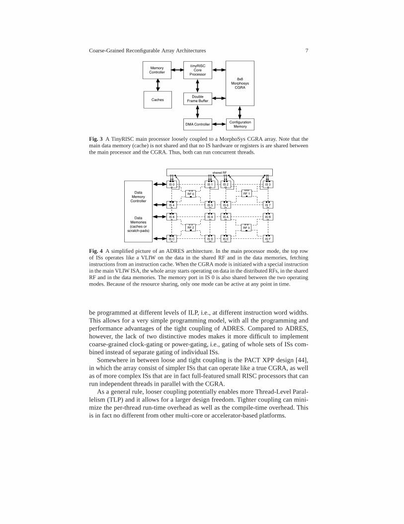
Some CGRA designs are coupled loosely to main processors. For example, Figure 3depicts how the MorphoSys CGRA [35] is connected as an external accelerator toa TinyRISC Central Processing Unit (CPU). The CPU is responsible for executingnon-loop code, for initiating DMA data transfers to and fromthe CGRA and thebuffers, and for initiating the operation of the CGRA itselfby means of specialinstructions added to the TinyRISC ISA.
This type of design offers the advantage that the CGRA and themain CPU can bedesigned independently, and that both can execute code concurrently, thus deliveringhigher parallelism and higher performance. For example, using the double framebuffers [35] depicted in Figure 3, the MorphoSys CGRA can be operating on datain one buffer while the main CPU initiates the necessary DMA transfers to the otherbuffer for the next loop or for the next set of loop iterations. One drawback is thatany data that needs to be transferred from non-loop code to loop code needs tobe transferred by means of DMA transfers. This can result in alarge overhead,e.g., when frequent switching between non-loop code and loops with few iterationsoccurs and when the loops consume scalar values computed by non-loop code.
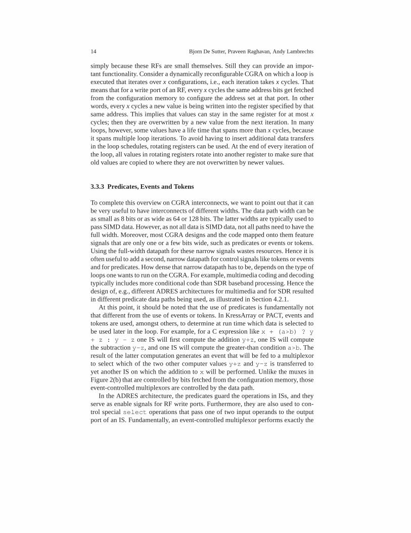
By contrast, an ADRES CGRA is coupled tightly to its main CPU.A simplifiedADRES is depicted in Figure 4. Its main CPU is a VLIW consisting of the sharedRF and the top row of CGRA ISs. In the main CPU mode, this VLIW executesinstructions that are fetched from a VLIW instruction cacheand that operate ondata in the shared RF. The idle parts of the CGRA are then disabled by clock-gatingto save energy. By executing astart CGRA instruction, the processor switches toCGRA mode in which the whole array, including the shared RF and the top rowof ISs, executes a loop for which it gets its configuration bits from a configurationmemory. This memory is omitted from the figure for the sake of simplicity.
The drawback of this tight coupling is that because the CGRA and the main pro-cessor mode share resources, they cannot execute code concurrently. However, thistight coupling also has advantages. Scalar values that havebeen computed in non-loop code, can be passed from the main CPU to the CGRA without any overheadbecause those values are already present in the shared RFs orin the shared memorybanks. Furthermore, using shared memories and an executionmodel of exclusiveexecution in either main CPU or CGRA mode significantly easesthe automatedco-generation of main CPU code and of CGRA code in a compiler,and it avoidsthe run-time overhead of transferring data. Finally, on theADRES CGRA, switch-ing between the two modes takes only two cycles. Thus, the run-time overhead isminimal.
Silicon Hive CGRAs [8, 9] do not feature a clear separation between the CGRAaccelerator and the main processor. Instead there is just a single processor that can
Coarse-Grained Reconfigurable Array Architectures 7�inyRISCCore
Processor
8x8MorphosysCGRA
Double Frame Buffer
DMA ControllerConfiguration Memory
Memory Controller
Caches
Fig. 3 A TinyRISC main processor loosely coupled to a MorphoSys CGRA array. Note that themain data memory (cache) is not shared and that no IS hardwareor registers is are shared betweenthe main processor and the CGRA. Thus, both can run concurrent threads.
shared RF
IS 0 IS 1 IS 2 IS 3
IS 4 IS 5 IS 6 IS 7
IS 8 IS 9 IS A IS B
IS C IS D IS E IS F
RF 0 RF 1
RF 3RF 2
DataMemory Controller
Data Memories (caches or
scratch-pads)
Fig. 4 A simplified picture of an ADRES architecture. In the main processor mode, the top rowof ISs operates like a VLIW on the data in the shared RF and in the data memories, fetchinginstructions from an instruction cache. When the CGRA mode is initiated with a special instructionin the main VLIW ISA, the whole array starts operating on datain the distributed RFs, in the sharedRF and in the data memories. The memory port in IS 0 is also shared between the two operatingmodes. Because of the resource sharing, only one mode can be active at any point in time.
be programmed at different levels of ILP, i.e., at differentinstruction word widths.This allows for a very simple programming model, with all theprogramming andperformance advantages of the tight coupling of ADRES. Compared to ADRES,however, the lack of two distinctive modes makes it more difficult to implementcoarse-grained clock-gating or power-gating, i.e., gating of whole sets of ISs com-bined instead of separate gating of individual ISs.
Somewhere in between loose and tight coupling is the PACT XPPdesign [44],in which the array consist of simpler ISs that can operate like a true CGRA, as wellas of more complex ISs that are in fact full-featured small RISC processors that canrun independent threads in parallel with the CGRA.
As a general rule, looser coupling potentially enables moreThread-Level Paral-lelism (TLP) and it allows for a larger design freedom. Tighter coupling can mini-mize the per-thread run-time overhead as well as the compile-time overhead. Thisis in fact no different from other multi-core or accelerator-based platforms.

8 Bjorn De Sutter, Praveen Raghavan, Andy Lambrechts
3.2 CGRA Control
There exist many different mechanisms to control how code gets executed onCGRAs, i.e., to control which operation is issued on which ISat which time andhow data values are transferred from producing operations to consuming ones. Twoimportant aspects of CGRAs that drive different methods forcontrol are reconfig-urability and scheduling. Both can be static or dynamic.
3.2.1 Reconfigurability
Some CGRAs, like ADRES, Silicon Hive, and MorphoSys are fully dynamicallyreconfigurable: exactly one full reconfiguration takes place for every execution cy-cle. Of course no reconfiguration takes places in cycles in which the whole array isstalled. Such stalls can happen, e.g., because memory accesses take longer than ex-pected in the schedule as a result of a cache miss or a memory bank access conflict.This cycle-by-cycle reconfiguration is similar to the fetching of one VLIW instruc-tion per cycle, but on these CGRAs the fetching is simpler as it only iterates througha loop body existing of straight-line CGRA configurations without control flow.Other CGRAs like the KressArray [24, 25, 26] are fully statically reconfigurable,meaning that the CGRA is configured before a loop is entered, and no reconfigu-ration takes place during the loop at all. Still other architectures feature a hybridreconfigurability. The RaPiD [14, 18] architecture features partial dynamic recon-figurability, in which part of the bits are statically reconfigurable and another partis dynamically reconfigurable and controlled by a small sequencer. Yet another ex-ample is the PACT architecture, in which the CGRA itself can initiate events thatinvoke (partial) reconfiguration. This reconfiguration consumes a significant amountof time, however, so it is advised to avoid it if possible, andto use the CGRA as astatically reconfigurable CGRA.
In statically reconfigured CGRAs, each resource performs a single task for thewhole duration of the loop. In that case, the mapping of software onto hardwarebecomes purely spatial, as illustrated in Figure 5(a). In other words, the mappingproblem becomes one of placement and routing, in which instructions and data de-pendencies between instructions have to mapped on a 2D arrayof resources. Forthese CGRAs, compiler techniques similar to hardware synthesis techniques can beused, as those used in FPGA placement and routing [3].
By contrast, dynamic reconfigurability enables the programmer to use hardwareresources for multiple different tasks during the execution of a loop or even duringthe execution of a single loop iteration. In that case, the software mapping problembecomes a spatial and temporal mapping problem, in which theoperations and datatransfers not only need to be placed and routed on and over thehardware resources,but in which they also need to be scheduled. A contrived example of a temporalmapping is depicted in Figure 5(b). Most compiler techniques [15, 17, 20, 39, 43,45, 46] for these architectures also originate from the FPGAplacement and routingworld. For CGRAs, the array of resources is not treated as a 2Dspatial array, but as

Coarse-Grained Reconfigurable Array Architectures 9
ins 0 ins 1
ins 2ins 3
ins 3ins 2
ins 1
ins 0
x-axis
y-axis
time axis
Fig. 5 Part (a) shows a spatial mapping of a sequence of four instructions on a statically reconfig-urable 2x2 CGRA. Edges denote dependencies, with the edge from instruction 3 to instruction 0denoting that instruction 0 from iterationi depends on instruction 3 from iterationi −1. So onlyone out of four ISs is utilized per cycle. Part (b) shows a temporal mapping of the same code on adynamically reconfigurable CGRA with only one IS. The utilization is higher here, at 100%.
a 3D spatial-temporal array, in which the third dimension models time in the formof execution cycles. Scheduling in this dimension is often based on techniques thatcombine VLIW scheduling techniques such as modulo scheduling [31, 49], withFPGA synthesis-based techniques [3]. Still other compilertechniques exist that arebased on constraint solving [55], or on integer-linear programming [1, 64].
The most important advantage of static reconfigurability isthe lack of reconfigu-ration overhead, in particular in terms of power consumption. For that reason, largearrays can be used that are still power-efficient. The disadvantage is that even in thelarge arrays the amount of resources constrains which loopscan be mapped.
Dynamically reconfigurable CGRAs can overcome this problemby spreadingthe computations of a loop iteration over multiple configurations. Thus a small dy-namically reconfigurable array can execute larger loops. The loop size is then notlimited by the array size, but by the array size times the depth of the reconfigurationmemories. For reasons of power efficiency, this depth is alsolimited, typically totens or hundreds of configurations, which suffices for most ifnot all inner loops.
A potential disadvantage of dynamically reconfigurable CGRAs is the powerconsumption of the configuration memories, even for small arrays, and of the con-figuration fetching mechanism. The disadvantage can be tackled in different ways.ADRES and MorphoSys tackle it by not allowing control flow in the loop bodies,thus enabling the use of very simple, power-efficient configuration fetching tech-niques similar to level-0 loop buffering [34]. Whenever control flow is found inloop bodies, such as for conditional statements, this control flow then first needs tobe converted into data flow, for example by means of predication and hyperblockformation [36]. While these techniques can introduce some initial overhead in thecode, this overhead typically will be more than compensatedby the fact that a moreefficient CGRA design can be used.
The MorphoSys design takes this reduction of the reconfiguration fetching logiceven further by limiting the supported code to Single Instruction Multiple Data(SIMD) code. In the two supported SIMD modes, all ISs in a row or all ISs in acolumn perform identical operations. As such only one IS configuration needs tobe fetched per row or column. As already mentioned, the RaPiDarchitecture limitsthe number of configuration bits to be fetched by making only asmall part of the

10 Bjorn De Sutter, Praveen Raghavan, Andy Lambrechts
configuration dynamically reconfigurable. Kim et al. provide yet another solutionin which the configuration bits of one column in one cycle are reused for the nextcolumn in the next cycle [30]. Furthermore, they also propose to reduce the powerconsumption in the configuration memories by compressing the configurations [29].
Still, dynamically reconfigurable designs exist that put norestrictions on the codeto be executed, and that even allow control flow in the inner loops. The Silicon Hivedesign is one such design. Unfortunately, no numbers on the power consumptionoverhead of this design choice are publicly available.
A general rule is that a limited reconfigurability puts more constraints on thetypes and sizes of loops that can be mapped. Which design provides the highest per-formance or the highest energy efficiency depends, amongst others, on the variationin loop complexity and loop size present in the applicationsto be mapped onto theCGRA. With large statically reconfigurable CGRAs, it is onlypossible to achievehigh utilization for all loops in an application if all thoseloops have similar com-plexity and size, or if they can be made so with loop transformations, and if theiterations are not dependent on each other through long-latency dependency cycles(as was the case in Figure 5). Dynamically reconfigurable CGRAs, by contrast, canalso achieve high average utilization over loops of varyingsizes and complexities,and with inter-iteration dependencies. That way dynamically reconfigurable CGRAscan achieve higher energy efficiency in the data path, at the expense of higher en-ergy consumption in the control path. Which design option isbest thus also dependson the process technology used, and in particular on the ability to perform clock orpower gating and on the ratio between active and passive power (a.k.a. leakage).
3.2.2 Scheduling and Issuing
Both with dynamic and with static reconfigurability, the execution of operations andof data transfers needs to be controlled. This can be done statically in a compiler,similar to the way in which operations from static code schedules are scheduled andissued on VLIW processors [19], or dynamically, similar to the way in which out-of-order processors issue instructions when their operands become available [54].Many possible combinations of static and dynamic reconfiguration and of static anddynamic scheduling exist.
A first class consists of dynamically scheduled, dynamically reconfigurableCGRAs like the TRIPS architecture [23, 51]. For this architecture, the compiler de-termines on which IS each operation is to be executed and overwhich connectionsdata is to be transferred from one IS to another. So the compiler performs placementand routing. All scheduling (including the reconfiguration) is dynamic, however, asin regular out-of-order superscalar processors [54]. TRIPS mainly targets general-purpose applications, in which unpredictable control flow makes the generation ofhigh-quality static schedules difficult if not impossible.Such applications most of-ten provide relatively limited ILP, for which large arrays of computational resourcesare not efficient. So instead a small, dynamically reconfigurable array is used, forwhich the run-time cost of dynamic reconfiguration and scheduling is acceptable.

Coarse-Grained Reconfigurable Array Architectures 11
A second class of dynamically reconfigurable architecturesavoids the overheadof dynamic scheduling by supporting VLIW-like static scheduling [19]. Instead ofdoing the scheduling in hardware where the scheduling logicthen burns power, thescheduling for ADRES, MorphoSys and Silicon Hive architectures is done by acompiler. Compilers can do this efficiently for loops with regular, predictable be-havior and high ILP, as found in many DSP applications. As forVLIW architec-tures, software pipelining [31, 49] is a very important to expose the ILP in softwarekernels, so most compiler techniques [15, 17, 20, 39, 43, 45,46] for staticallyscheduled CGRAs implement some form of software pipelining.
A final class of CGRAs are the statically reconfigurable, dynamically scheduledarchitectures, such as KressArray or PACT (neglecting the time-consuming partialreconfigurability of the PACT). The compiler performs placement and routing, andthe code execution progress is guided by tokens or event signals that are passedalong with data. Thus the control is dynamic, and it is distributed over the token orevent path, similar to the way in which transport-triggeredarchitectures [13] oper-ate. These statically reconfigurable CGRAs do not require software pipelining tech-niques because there is no temporal mapping. Instead the spatial mapping and thecontrol implemented in the tokens or event signals implement a hardware pipeline.
We can conclude by noting that, as in other architecture paradigms such as VLIWprocessing or superscalar out-of-order execution, dynamically scheduled CGRAscan deliver higher performance than statically scheduled ones for control-intensivecode with unpredictable behavior. On dynamically scheduled CGRAs the code paththat gets executed in an iteration determines the executiontime of that iteration,whereas on statically scheduled CGRAs, the combination of all possible executionpaths (including the slowest path which might be executed infrequently) determinesthe execution time. Thus, dynamically scheduled CGRAs can provide higher per-formance for some applications. However, the power efficiency will then typicallyalso be poor because more power will be consumed in the control path. Again, theapplication domain determines which design option is most appropriate.
3.2.3 Thread-level and Data-level Parallelism
Another important aspect of control is the possibility to support different formsof parallelism. Obviously, loosely-coupled CGRAs can operate in parallel with themain CPU, but one can also try to use the CGRA resources to implement SIMD orto run multiple threads concurrently within the CGRA.
When dynamic scheduling is implemented via distributed event-based control, asin KressArray or PACT, implementing TLP is relatively simple and cheap. For smallenough loops of which the combined resource use fits on the CGRA, it suffices tomap independent thread controllers on different parts of the distributed control.
For architectures with centralized control, the only option to run threads in paral-lel is to provide additional controllers or to extend the central controller, for exampleto support parallel execution modes. While such extensionswill increase the power

12 Bjorn De Sutter, Praveen Raghavan, Andy Lambrechts
consumption of the controller, the newly supported modes might suit certain codefragments better, thus saving in data path energy and configuration fetch energy.
The TRIPS controller supports four operation modes [51]. Inthe first mode, allISs cooperate for executing one thread. In the second mode, the four rows executefour independent threads. In the third mode, fine-grained multi-threading [54] issupported by time-multiplexing all ISs over multiple threads. Finally, in the fourthmode each row executes the same operation on each of its ISs, thus implementingSIMD in a similar, fetch-power-efficient manner as is done inthe two modes of theMorphoSys design. Thus, for each loop or combination of loops in an application,the TRIPS compiler can exploit the most suited form of parallelism.
The Raw architecture [57] is a hybrid between a many-core architecture and aCGRA architecture in the sense that it does not feature a 2D array of ISs, but rathera 2D array of tiles that each consist of a simple RISC processor. The tiles are con-nected to each other via a mesh interconnect, and transporting data over this inter-connect to neighboring tiles does not consume more time thanretrieving data fromthe RF in the tile. Moreover, the control of the tiles is such that they can operate in-dependently or synchronized in a lock-step mode. Thus, multiple tiles can cooperateto form a dynamically reconfigurable CGRA. A programmer can hence partition the2D array of tiles into several, potentially differently sized, CGRAs that each run anindependent thread. This provides very high flexibility to balance the available ILPinside threads with the TLP of the combined threads.
Other architectures do not support (hardware) multi-threading within one CGRAcore at all, like the current ADRES and Silicon Hive. The firstsolution to run multi-ple threads with these designs is to incorporate multiple CGRA accelerator cores ina System-on-Chip (SoC). The advantage is then that each accelerator can be cus-tomized for a certain class of loop kernels. Also, ADRES and Silicon Hive arearchitecture templates, which enables CGRA designers to customize their CGRAcores for the appropriate amount of DLP for each class of loopkernels, in the formof SIMD or subwordparallelism.
Alternatively, TLP can be converted into ILP and DLP by combining, at compile-time, kernels of multiple threads and by scheduling them together as one kernel, andby selecting the appropriate combination of scheduled kernels at run time [52].
3.3 Interconnects and Register Files
3.3.1 Connections
A wide range of connections can connect the ISs of a CGRA with each other, andwith the RFs, other memories and IO ports. Buses, point-to-point connections, andcrossbars are all used in various combinations and in different topologies.
For example, some designs like MorphoSys and the most commonADRESand Silicon Hive designs feature a densely connected mesh-network of point-to-point interconnects in combination with sparser buses thatconnect ISs further apart.

Coarse-Grained Reconfigurable Array Architectures 13
Thus the number of long power-hungry connections is limited. Multiple studies ofpoint-to-point mesh-like interconnects as in Figure 10 have been published in thepast [7, 28, 32, 38]. Other designs like RaPiD feature a densenetwork of segmentedbuses. Typically the use of crossbars is limited to very small instances because largeones are too power-hungry. Fortunately, large crossbars are most often not needed,because many application kernels can be implemented as systolic algorithms, whichmap well onto mesh-like interconnects as found in systolic arrays [47].
Unlike crossbars and even busses, mesh-like networks of point-to-point connec-tions scale better to large arrays without introducing too much delay or power con-sumption. For statically reconfigurable CGRAs, this is beneficial. Buses and otherlong interconnects connect whole rows or columns to complement short-distancemesh-like interconnects. The negative effects that such long interconnects can haveon power consumption or on obtainable clock frequency can beavoided by segmen-tation or by pipelining. In the latter case, pipelining latches are added along the con-nections or in between muxes and ISs. Our experience, as presented in Section 4.2.2is that this pipelining will not necessarily lead to lower IPCs in CGRAs. This is dif-ferent from out-of-order or VLIW architectures, where deeper pipelining increasesthe branch misprediction latency [54]. Instead at least some CGRA compilers suc-ceed in exploiting the pipelining latches as temporary storage, rather than beinghampered by them. This is the case in compiler techniques like [15, 39] that arebased on FPGA synthesis methods in which RFs and pipelining latches are treatedas interconnection resources that span multiple cycles instead of as explicit storageresources. This treatment naturally fits the 3D array modeling of resources alongtwo spatial dimensions and one temporal dimension. Consequently, those compilertechniques can exploit pipelining latches naturally and similarly to using storagespace in distributed RFs.
3.3.2 Register Files
Compilers for CGRA architectures place operations in ISs, thus also schedulingthem, and route the data flow over the connections between theISs. Those connec-tions may be direct connections, or latched connections, oreven connections that gothrough RFs. Therefore most CGRA compilers treat RFs not as temporary storage,but as interconnects that can span multiple cycles. Thus theRFs can be treated uni-formly with the connections during routing. A direct consequence of this compilerapproach is that the design space freedom of interconnects extends to the placementof RFs in between ISs. During the DSE for a specific CGRA instance in a CGRAdesign template such as the ADRES or Silicon Hive templates,both the real con-nections and the RFs have to be explored, and that has to be done together. Just likethe number of real interconnect wires and their topology, the size of RFs, their lo-cation and their number of ports then contribute to the interconnectivity of the ISs.We refer to [7, 38] for DSEs that study both RFs and interconnects.
Besides their size and ports, another important aspect is that RFs can be rotat-ing [50]. The power and delay overhead of rotation is very small in distributed RFs,
14 Bjorn De Sutter, Praveen Raghavan, Andy Lambrechts
simply because these RFs are small themselves. Still they can provide an impor-tant functionality. Consider a dynamically reconfigurableCGRA on which a loop isexecuted that iterates overx configurations, i.e., each iteration takesx cycles. Thatmeans that for a write port of an RF, everyx cycles the same address bits get fetchedfrom the configuration memory to configure the address set at that port. In otherwords, everyx cycles a new value is being written into the register specified by thatsame address. This implies that values can stay in the same register for at mostxcycles; then they are overwritten by a new value from the nextiteration. In manyloops, however, some values have a life time that spans more thanx cycles, becauseit spans multiple loop iterations. To avoid having to insertadditional data transfersin the loop schedules, rotating registers can be used. At theend of every iteration ofthe loop, all values in rotating registers rotate into another register to make sure thatold values are copied to where they are not overwritten by newer values.
3.3.3 Predicates, Events and Tokens
To complete this overview on CGRA interconnects, we want to point out that it canbe very useful to have interconnects of different widths. The data path width can beas small as 8 bits or as wide as 64 or 128 bits. The latter widthsare typically used topass SIMD data. However, as not all data is SIMD data, not all paths need to have thefull width. Moreover, most CGRA designs and the code mapped onto them featuresignals that are only one or a few bits wide, such as predicates or events or tokens.Using the full-width datapath for these narrow signals wastes resources. Hence it isoften useful to add a second, narrow datapath for control signals like tokens or eventsand for predicates. How dense that narrow datapath has to be,depends on the type ofloops one wants to run on the CGRA. For example, multimedia coding and decodingtypically includes more conditional code than SDR basebandprocessing. Hence thedesign of, e.g., different ADRES architectures for multimedia and for SDR resultedin different predicate data paths being used, as illustrated in Section 4.2.1.
At this point, it should be noted that the use of predicates isfundamentally notthat different from the use of events or tokens. In KressArray or PACT, events andtokens are used, amongst others, to determine at run time which data is selected tobe used later in the loop. For example, for a C expression likex + (a>b) ? y+ z : y - z one IS will first compute the additiony+z, one IS will computethe subtractiony-z, and one IS will compute the greater-than conditiona>b. Theresult of the latter computation generates an event that will be fed to a multiplexorto select which of the two other computer valuesy+z andy-z is transferred toyet another IS on which the addition tox will be performed. Unlike the muxes inFigure 2(b) that are controlled by bits fetched from the configuration memory, thoseevent-controlled multiplexors are controlled by the data path.
In the ADRES architecture, the predicates guard the operations in ISs, and theyserve as enable signals for RF write ports. Furthermore, they are also used to con-trol specialselect operations that pass one of two input operands to the outputport of an IS. Fundamentally, an event-controlled multiplexor performs exactly the

Coarse-Grained Reconfigurable Array Architectures 15
(a) MorphoSys issue slot (b) ADRES issue slot
LOCAL RF
4 registers
src 0 mux
src 1 mux
ALU + MULT
feedback
latch
shift
latch
any combinationof operations
pred mux
src 0 mux
flag
src 1 mux
opt src 3 mux
optional
pipe latch
optional
pipe latch
optional
pipe latch
optional
pipe latch
optional
pipe latch
ALU + MULT ALU + MULT
ALU + MULT ALU + MULT
src 0 mux
src 1 mux
src 0 mux
src 1 mux
LOCAL
RF
(c) a single issue slot as proposed by Galanis et al.
IS 0
ALU
IS 1
ALU
IS 2
ALU
IS 3
ALU
shared
MULsw sw sw sw
(d) issue slots that share a multiplier
Fig. 6 Four different structures of ISs proposed in the literature. Part (a) displays a fixed Mor-phoSys IS, including its local RF. Part (b) displays the fully customizable ADRES IS, that canconnect to shared or non-shared local RFs. Part (c) depicts the IS structure proposed by Galanis etal. [22], and (d) depicts a row of four ISs that share a multiplier [27].
same function as theselect operation. So the difference between events or to-kens and predicates is really only that the former term and implementation are usedin dynamically scheduled designs, while the latter term is used in static schedules.
3.4 Computational Resources
Issue slots are the computational resources of CGRAs. Over the last decade, nu-merous designs of such issue slots have been proposed, underdifferent names, thatinclude PEs, FUs, ALUs, and flexible computation components. Figure 6 depictssome of them. For all of the possible designs, it is importantto know the contextin which these ISs have to operate, such as the interconnectsconnecting them, thecontrol type of the CGRA, etc.
Figure 6(a) depicts the IS of a MorphoSys CGRA. All 64 ISs in this homoge-neous CGRA are identical and include their own local RF. Thisis no surprise, as thetwo MorphoSys SIMD modes (see Section 3.2.1) require that all ISs of a row or ofa column execute the same instruction, which clearly implies homogeneous ISs.

16 Bjorn De Sutter, Praveen Raghavan, Andy Lambrechts
In contrast, almost all features of an ADRES IS, as depicted in Figure 6(b), canbe chosen at design time, and can be different for each IS in a CGRA that then be-comes heterogeneous: the number of ports, whether or not there are latches betweenthe multiplexors and the combinatorial logic that implements the operations, the setof operations supported by each IS, how the local registers file are connected to ISsand possibly shared between ISs, etc. As long as the design instantiates the ADREStemplate, the ADRES tool flow will be able to synthesize the architecture and to gen-erate code for it. A similar design philosophy is followed bythe Silicon Hive tools.Of course this requires more generic compiler techniques than those that generatecode for the predetermined homogeneous ISs of, e.g., the MorphoSys CGRA. Giventhe state of the art in compiler technology for this type of architecture, the advan-tages of this freedom are (1) the possibility to design different instances optimizedfor certain application domains, (2) the knowledge that thefeatures of those de-signs will be exploited, and (3) the ability to compile loopsthat feature other formsof ILP than DLP. DLP can still be supported, of course, by simply incorporatingSIMD-capable (a.k.a. subwordparallel) ISs of, e.g., 4x16 bits wide. The drawbackis this design freedom is that, at least with the current compiler techniques, thesetechniques are so generic that they miss optimization opportunities because theydo not exploit regularity in the designed architectures. They do not exploit it forspeeding up the compilation, nor do they for producing better schedules.
Figure 6(c) depicts the IS proposed by Galanis et al. [22]. Again, all ISs are iden-tical. In contrast to the MorphoSys design, however, these ISs consist of severalALUs and multipliers with direct connections between them and their local RFs.These direct connections within each IS can take care of a lotof data transfers, thusfreeing time on the shared bus-based interconnect that connects all ISs. Thus, thelocal interconnect within each IS compensates for the lack of a scaling global inter-connect. One advantage of this approach is that the compilercan be tuned specif-ically for this combination of local and global connectionsand for the fact that itdoes not need to support heterogeneous ISs. Whether or not this type of design ismore power-efficient than that of CGRAs with more design freedom and potentiallymore heterogeneity is unclear at this point in time. At least, we know of no studiesfrom which, e.g., utilization numbers can be derived that allow us to compare thetwo approaches.
With respect to utilization, it is clear that the designs of Figure 6(a) and 6(b) willonly be utilized well if a lot of multiplications need to be performed. Otherwise,the area-consuming multipliers remain unused. To work around this problem, thesharing of large resources such as multipliers between ISs has been proposed in theRSPA CGRA design [27]. Figure 6(d) depicts one row of ISs thatdo not containmultipliers internally, but that are connected to a shared multiplier through switchesand a shared bus. The advantage of this design, compared to anADRES designin which each row features 3 pure ALU ISs and 1 ALU+MULT IS, is that thisdesign allows the compiler to schedule multiplications in all ISs (albeit only oneper cycle), whereas this scheduling freedom would be limited to one IS slot in theADRES design. To allow this schedule freedom, however, a significant amount ofresources in the form of switches and a special-purpose bus need to be added to the

Coarse-Grained Reconfigurable Array Architectures 17
row. While we lack experimental data to back up this claim, wefirmly believe thata similar increase in schedule freedom can be obtained in theaforementioned 3+1ADRES design by simply extending an existing ADRES interconnect with a similaramount of additional resources. In the ADRES design, that extension would thenalso be beneficial to operations other than multiplications.
The optimal number of ISs for a CGRA depends on the application domain, onthe reconfigurability, as well as on the IS functionality andon the DLP available inthe form of subwordparallelism. As illustrated in section 4.2.2, a typical ADRESwould consist of 4x4 ISs [6, 37]. TRIPS also features 4x4 ISs.MorphoSys provides8x8 ISs, but that is because the DLP is implemented as SIMD over multiple ISs,rather than as subwordparallelism within ISs. In our experience, scaling dynamicallyreconfigurable CGRA architectures such as ADRES to very large arrays (8x8 orlarger) does not make sense even with scalable interconnects like mesh or mesh-plus interconnects. Even in loops with high ILP, utilization drops significantly onsuch large arrays [42]. It is not yet clear what is causing this lower utilization, andthere might be several reasons. These include a lack of memory bandwidth, thepossibility that the compiler techniques [15, 39] simply donot scale to such largearrays, or the fact that the relative connectivity in such large arrays is lower. Simplystated, when a mesh interconnects all ISs to their neighbors, each IS not on the sideof the array is connected to 4 other ISs out of 16 in a 4x4 array,i.e., to 25% of allISs, while it is connected to 4 out of 64 ISs on an 8x8 array, i.e., to 6.25% of all ISs.
To finalize this section, we want to mention that, just like inany other type ofprocessor, it makes sense to pipeline complex combinatorial logic, e.g., as foundin multipliers. There are no fundamental problems to do this, and it can lead tosignificant increases in utilization and clock frequency.
3.5 Memory Hierarchies
CGRAs have a large number of ISs that need to be fed with data from the memory.Therefore the data memory sub-system is a crucial part of theCGRA design. Manyreconfigurable architectures feature multiple independent memory banks or blocksto achieve high data bandwidth. Exploiting those automatically in a compiler hasnot yet been fully solved.
The RAW architecture features an independent memory block in each tile forwhich Barua developed a method called modulo unrolling to disambiguate and as-sign data to different banks [2]. However, this technique can only handle array ref-erences through affine index expression on loop induction variables.
MorphoSys has a 256-bit wide frame buffer between the main memory and areconfigurable array to feed data to the ISs operating in SIMDmode [35]. The ef-ficient use of such a wide memory depends by and large on manualdata placementand operation scheduling. Similar techniques for wide loads and stores have alsobeen proposed in regular VLIW architectures for reducing power [48]. However,

18 Bjorn De Sutter, Praveen Raghavan, Andy Lambrechts
this requires the programmer or compiler to perform the datalayout in memory inorder to exploit the large bandwidth between the level-1 memory and the datapath.
Both Silicon Hive and PACT feature distributed memory blocks without a cross-bar. A Silicon Hive programmer has to specify the allocationof data to the memoryfor the compiler to bind the appropriate load/store operations to the correspondingmemories. Silicon Hive also supports the possibility of interfacing the memory orsystem bus using FIFO interfaces. This is efficient for streaming processing but isdifficult to interface when the data needs to be buffered on incase of data reuse.
The ADRES architecture template provides a parameterizable Data MemoryQueue (DMQ) interface to each of the different single-ported, interleaved level-1 scratch-pad memory banks [6]. The DMQ interface is responsible for resolvingbank access conflicts, i.e., when multiple load/store ISs would want to access thesame bank at the same time. Connecting all load/store ISs to all banks through aconflict resolution mechanism allows maximal freedom for data access patterns andalso maximal freedom on the data layout in memory. The potential disadvantage ofsuch conflict resolution is that it increases the latency of load operations. In soft-ware pipelined code, however, increasing the individual latency of instructions mostoften does not have a negative effect on the schedule quality, because the compilercan hide those latencies in the software pipeline. In the main processor VLIW modeof an ADRES, that accesses the same memories in code not software-pipelined, theconflict resolution is disabled to obtain shorter access latencies.
3.6 Compiler Support
Apart from the specific algorithms used to compile code, the major distinctions be-tween the different existing compiler techniques relate towhether or not they sup-port static scheduling, whether or not they support dynamicreconfiguration, whetheror not they rely on special programming languages, and whether or not they are lim-ited to specific hardware properties. Because most compilerresearch has been doneto generate static schedules for CGRAs, we focus on those in this section. As al-ready indicated in Sections 3.2.1 and 3.2.2, many algorithms are based on FPGAplacement and routing techniques [3] in combination with VLIW code generationtechniques like modulo scheduling [31, 49] and hyperblock formation [36].
Whether or not compiler techniques rely on specific hardwareproperties is not al-ways obvious in the literature, as not enough details are available in the descriptionsof the techniques, and few techniques have been tried on a wide range of CGRA ar-chitectures. For that reason, it is very difficult to comparethe efficiency (compilationtime) and effectiveness (quality of generated code) of the different techniques.
The most widely applicable static scheduling techniques use different forms ofModulo Resource Routing Graphs (MRRGs). RRGs are time-space graphs, in whichall resources (space dimension) are modeled with vertices.There is one such ver-tex per resource per cycle (time dimension) in the schedule being generated. Di-rected edges model the connections over which data values can flow from resource
Coarse-Grained Reconfigurable Array Architectures 19
to resource. The schedule, placement and routing problem than becomes a problemof mapping the Data Dependence Graph (DDG) of some loop body on the RRG.Scheduling refers to finding the right cycle to perform an operation in the schedule,placement refers to finding the right IS in that cycle, and routing refers to findingconnections to transfer data from producing operations to consuming operations. Inthe case of a modulo scheduler, the modulo constraint is enforced by modeling allresource usage in the modulo time domain. This is done by modeling the appropriatemodulo reservation tables [49] on top of the RRG, hence the name MRRG.
The granularity of its vertices depends on the precise compiler algorithm. Onemodulo graph embedding algorithm [45] models whole ISs or whole RFs withsingle vertices, whereas the simulated-annealing technique in the DRESC [15, 39]compiler that targets ADRES instances models individual ports to ISs and RFs asseparate vertices. Typically, fewer nodes that model larger components lead to fastercompilation because the graph mapping problem operates on asmaller graph, butalso to lower code quality because some combinations of resource usage cannot bemodeled precisely. Some techniques, such as DRESC, are built on the central idea offinding the best routes to steer the placement and scheduling, thus exploring manypossible routings, while others [20, 43, 45, 46] use heuristics to place and sched-ule the code, using routability as a constraint during the scheduling. The latter aretypically much more efficient, but less effective.
MRRG-based compiler techniques are easily retargetable toa wide range of ar-chitectures, such as those of the ADRES template, and they can support many pro-gramming languages. Different architectures can simply bemodeled with differentMRRGs. To support different programming languages like C and Fortran, the tech-niques only require a compiler front-end that is able to generate DDGs for the loopbodies. Obviously, the appropriate loop transformations need to be applied beforegenerating the DDG in order to generate one that maps well onto the MRRG of thearchitecture. Such loop transformations are discussed in detail in Section 4.1.
Many other CGRA compiler techniques have been proposed, most of which arerestricted to specific architectures. Static reconfigurable architectures like RaPiDand PACT have been targeted by compiler algorithms [10, 17, 63] based on place-ment and routing techniques that also map DDGs on RRGs. Thesetechniques sup-port subsets of the C programming language (no pointers, no structs, ...) and requirethe use of special C functions to program the IO in the loop bodies to be mappedonto the CGRA. The latter requirement follows from the specific IO support in thearchitectures and the modeling thereof in the RRGs.
For the MorphoSys architecture, with its emphasis on SIMD across ISs, compilertechniques have been developed for the SA-C language [61]. In this language thesupported types of available parallelism are specified by means of loop languageconstructs. These constructs are translated into control code for the CGRA, whichare mapped onto the ISs together with the DDGs of the loop bodies.
CGRA code generation techniques based on integer-linear programming havebeen proposed for the RSPA architecture, both for spatial [1] and for temporal map-ping [64]. Basically, the ILP formulation consists of all the requirements or con-straints that must be met by a valid schedule. This formulation is built from a DDG

20 Bjorn De Sutter, Praveen Raghavan, Andy Lambrechts
and a hardware description, and can hence be used to compile many source lan-guages. It is unclear, however, to what extent the ILP formulation and its solutionrely on specific architecture features, and hence to which extent it would be possi-ble to retarget the ILP-formulation to different CGRA designs. A similar situationoccurs for the constraint-based compilation method developed for the Silicon Hivearchitecture template [55], of which no detailed information is public.
Code generation techniques for CGRAs based on instruction-selection patternmatching and list-scheduling techniques have also been proposed [21, 22]. It is un-clear to what extent these techniques rely a on specific architecture because weknow of no trial to use them for different CGRAs, but these techniques seem torely heavily on the existence of a single shared-bus that connects ISs as depictedin Figure 6(c). Similarly, the static reconfiguration code generation technique byLee et al. relies on CGRA rows consisting of identical ISs [33]. Because of thisassumption, a two-step code generation approach can be usedin which individualplacements within rows are neglected in the first step, and only taken care of in thesecond step. The first step then instead focuses on optimizing the memory traffic.
Finally, compilation techniques have been developed that are really specializedfor the TRIPS array layout and for its out-of-order execution [12].
One rule-of-thumbcovers all the mentioned techniques: more generic techniques,i.e., techniques that are more flexible in targeting different architectures or differentinstances of an architecture template, are less efficient and often less effective inexploiting special architecture features. In other words techniques that rely on spe-cific hardware features, such as interconnect regularitiesor specific forms of ISsclustering, while being less flexible, will generally be able to target those hardwarefeatures more efficiently, and often also more effectively.Vice versa, architectureswith such features usually need specialized compiler techniques. This is similar tothe situation of more traditional DSP or VLIW architectures.
4 Case Study: ADRES
This section presents a case study on one specific CGRA designtemplate. The pur-pose of this study is to illustrate that it is non-trivial to compile and optimize codefor CGRA targets, and to illustrate that within a design template, there is a needfor hardware design exploration. This illustrates how bothhardware and softwaredesigners targeting CGRAs need a deep understanding of the interaction betweenthe architecture features and the used compiler techniques.
ADRES [5, 6, 7, 15, 37, 39, 40, 41] is an architecture design template fromwhich dynamically reconfigurable, statically scheduled CGRAs can be instantiated.In each instance, an ADRES CGRA is coupled tightly to a VLIW processor. Thisprocessor shares data and predicate RFs with the CGRA, as well as memory portsto a multi-banked scratch-pad memory as described in Section 3.1. The compiler-supported ISA of the design template provides instructionsthat are typically foundin a load/store VLIW or RISC architecture, including arithmetic operations, logic

Coarse-Grained Reconfigurable Array Architectures 21
operations, load/store operations, and predicate computing instructions. Additionaldomain-specific instructions, such as SIMD operations, aresupported in the pro-gramming tools by means of intrinsics [56]. Local rotating and non-rotating, sharedand private local RFs can be added to the CGRA as described in the previoussections, and connected through an interconnect consisting of muxes, buses andpoint-to-point connections that are specified completely by the designer. Thus, theADRES architecture template is very flexible: it offers a high degree of design free-dom, and it can be used to accelerate a wide range of loops.
4.1 Mapping Loops onto ADRES CGRAs
The first part of this case study concerns the mapping of loopsonto ADRES CGRAs,which are one of the most flexible CGRAs supporting a wide range of loops. Thisstudy illustrates that many loop transformations need to beapplied carefully be-fore mapping code onto ADRES CGRAs. We discuss the most important compilertransformations and, lacking a full-fledged loop-optimizing compiler, manual looptransformations that need to be applied to source code in order to obtain high per-formance and high efficiency. For other, less flexible CGRAs,the need for suchtransformations will even be higher because there will be more constraints on theloops to be mapped in the first place. Hence many of the discussed issues not onlyapply to ADRES CGRAs, but also to other CGRA architectures. We will concludefrom this study that programming CGRAs with the existing compiler technology isnot compatible with high programmer productivity.
4.1.1 Modulo Scheduling Algorithms for CGRAs
To exploit ILP in inner loops on VLIW architectures, compilers typically applysoftware pipelining by means of modulo scheduling [31, 49].This is no differentfor ADRES CGRAs. In this section, we will not discuss the inner working of mod-ulo scheduling algorithms. What we do discuss, are the consequences of using thattechnique for programming ADRES CGRAs.
After a loop has been modulo-scheduled, it consists of threephases: the prologue,the kernel and the epilogue. During the prologue, stages of the software-pipelinedloop gradually become active. Then the loop executes the kernel in a steady-statemode in which all software pipeline stages are active, and afterwards the stages aregradually disabled during the epilogue. In the steady-state mode, a new iterationis started after everyII cycles, which stands for Initiation Interval. Fundamentally,every software pipeline stage isII cycles long. The total cycle count of a loop withiter iterations that is scheduled overpssoftware pipeline stages is then given by
cyclesprologue+ II · (iter− (ps−1))+cyclesepilogue. (2)

22 Bjorn De Sutter, Praveen Raghavan, Andy Lambrechts
In this formula, we neglect processor stalls because of, e.g., memory access conflictsor cache misses.
For loops with a high number of iterations, the termII · iter dominates this cy-cle count, and that is why modulo scheduling algorithms try to minimize II , thusincreasing the IPC terms in Equation (1).
The minimalII that modulo scheduling algorithms can reach is bound byminII =max(RecMII,ResMII). The first term, called resource-minimalII (ResMII) is de-termined by the resources required by a loop and by the resources provided by thearchitecture. For example, if a loop body contains 9 multiplications, and there areonly two ISs that can execute multiplications, then at least⌈9/2⌉ = 5 cycles willbe needed per iteration. The second term, called recurrence-minimal II (RecMII)depends on recurrent data dependencies in a loop and on instruction latencies. Fun-damentally, if an iteration of a loop depends on the previousiteration through adependency chain with accumulated latencyRecMII, it is impossible to start thatiteration before at leastRecMIIcycles of the previous iteration have been executed.
The next section uses this knowledge to apply transformations that optimize per-formance according to Equation (1). To do so successfully, it is important to knowthat ADRES CGRAs support only one thread, for which the processor has to switchfrom a non-CGRA operating mode to CGRA mode and back for each inner loop.So besides minimizing the cycle count of Equation (2) to obtain higher IPCs inEquation (1), it is also important to consider the termstp→p+1 in Equation (1).
4.1.2 Loop Transformations
Loop Unrolling
Loop unrolling and the induction variable optimizations that it enables can be usedto minimize the number of iterations of a loop. When a loop body is unrolledx times,iter decreases with a factorx, andResMIItypically grows with a factor slightly lessthanx because of the induction variable optimizations and because of the ceilingoperation in the computation ofResMII. By contrast,RecMII typically remainsunchanged or increases only a little bit as a result of the induction variable opti-mizations that are enabled after loop unrolling.
In resource-bound loops,ResMII> RecMII. Unrolling will then typically havelittle impact on the dominating termII · iter in Equation (2). However, the prologueand the epilogue will typically become longer because of loop unrolling. Moreover,an unrolled loop will consume more space in the instruction memory, which mightalso have a negative impact on the total execution time of thewhole application. Soin general, unrolling resource-bound loops is unlikely to be very effective.
In recurrence-bound loops,RecMII· iter > ResMII· iter. The right hand side ofthis inequality will not increase by unrolling, while the left hand side will be di-vided by the unrolling factorx. As this improvement typically compensates for thelonger prologue and epilogue, we can conclude that unrolling can be an effectiveoptimization technique for recurrence-bound loops if the recurrences can be opti-

Coarse-Grained Reconfigurable Array Architectures 23
mized with induction variable optimizations. This is no different for CGRAs thanit is for VLIWs. However, for CGRAs with their larger number of ISs, it is moreimportant because more loops are recurrence-bound.
Loop Fusion, Loop Interchange, Loop Combination and Data Context Switching
Fusing adjacent loops with the same number of iterations into one loop can also beuseful, because fusing multiple recurrence-bound loops can result in one resource-bound loop, which will result in a lower overall execution time. Furthermore, lessswitching between operating modes takes place with fused loops, and hence thetermstp→p+1 are minimized. Furthermore, less prologues and epilogues need to beexecuted, which might also improve performance. This improvement will usuallybe limited, however, because the fused prologues and epilogues will rarely be muchshorter than the sum of the original ones. Moreover, loop fusion does result in aloop that is bigger than any of the original loops, so it can only be applied if theconfiguration memory is big enough the fit the fused loop. If this is the case, lessloop configurations need to be stored and possibly reloaded into the memory.
Interchanging an inner and outer loop serves largely the same purpose as loopfusion. As loop interchange does not necessarily result in larger prologues and epi-logues, it can be even more useful, as can be the combining of nested loops into asingle loop. Data-context switching [4] is a very similar technique that serves thesame purpose. That technique has been used by Lee et al. for statically reconfig-urable CGRAs as well [33], and in fact most of the loop transformations mentionedin this section can be used to target such CGRAs, as well as anyother type of CGRA.
Live-in Variables
In our experience, there is only one caveat with the above transformations. Thereason to be careful when applying them is that they can increase the number oflive-in variables. A live-in variable is a variable that gets assigned a value before theloop, which is consequently used in the loop. Live-in variables can be manifest in theoriginal source code, but they can also result from compileroptimizations that areenabled by the above loop transformations, such as induction variable optimizationsand loop-invariant code motion. When the number of live-in variables increases,more data needs to be passed from the non-loop code to the loopcode, which mighthave a negative effect ontp→p+1. The existence and the scale of this effect willusually depend on the hardware mechanism that couples the CGRA accelerator tothe main core. Possible such mechanisms are discussed in Section 3.1. In tightly-coupled designs like that of ADRES or Silicon Hive, passing alimited amount ofvalues from the main CPU mode to the CGRA mode does not involveany overhead:the values are already present in the shared RF. However, if their number grows toobig, there will not be enough room in the shared RF, which willresult in much lessefficient passing of data through memory. We have experienced this several times

24 Bjorn De Sutter, Praveen Raghavan, Andy Lambrechts
with loops in multimedia and SDR applications that were mapped onto our ADRESdesigns. So, even for tightly-coupled CGRA designs, the above loop transformationsand the enabled optimizations need to be applied with great care.
Predication
Modulo scheduling techniques for CGRAs [15, 17, 20, 39, 45, 46] only scheduleloops that are free of control flow transfers. Hence any loop body that containsconditional statements first needs to be if-converted into hyperblocks by means ofpredication [36]. For this reason, many CGRAs, including ADRES CGRAs, supportpredication.
Hyperblock formation can result in very inefficient code if aloop body containscode paths that are executed rarely. All those paths contribute toResMII and po-tentially toRecMII. Hence even paths that get executed very infrequently can slowdown a whole modulo-scheduled loop. Such loops can be detected with profiling,and if the data dependencies allow this, it can be useful to split these loops intomultiple loops. For example, a first loop can contain the codeof the frequently ex-ecuted paths only, with a lowerII than the original loop. If it turns out during theexecution of this loop that in some iteration the infrequently executed code needs tobe executed, the first loop is exited, and for the remaining iterations a second loop isentered that includes both the frequently and the infrequently executed code paths.
Alternatively, for some loops it is beneficial to have a so-called inspector loopwith very smallII to perform only the checks for all iterations. If none of the checksare positive, a second so-called executor loop is executed that includes all the com-putations except the checks and the infrequently executed paths. If some checkswere positive, the original loop is executed.
One caveat with this loop splitting is that it causes code size expansion in theCGRA instruction memories. For power consumption reasons,these memories arekept as small as possible. This means that the local improvements obtained with theloop splitting need to be balanced with the total code size ofall loops that need toshare these memories.
Kernel-Only Loops
Predication can also be used to generate so-called kernel-only loop code. This isloop code that does not have separate prologue and epilogue code fragments. Insteadthe prologues and epilogues are included in the kernel itself, where predication isnow used to guard whole software pipeline stages and to ensure that only the appro-priate software pipeline stages are activated at each pointin time. A traditional loopwith a separate prologue and epilogue is compared to a kernel-only loop in Figure 7.Three observations need to be made here.
The first observation is that kernel-only code is usually faster because the pipelinestages of the prologue and epilogue now get executed on the CGRA accelerator,

Coarse-Grained Reconfigurable Array Architectures 25�2
3
4
1
2
3
4
1
2
3
4
1
2
3
4
1
2
3
4
1
2
3
4
1
2
3
4
1
2
3
4
prologueon main core
kernelon CGRA
epilogueon main core
original loop iterations
1
2
3
4
1
2
3
4
1
2
3
4
1
2
3
4
1
2
3
4
1
2
3
4
1
2
3
4
1
2
3
4
kernel-onlyon CGRA
original loop iterations
time
4
34
234
1
2
3
1
2 1
Fig. 7 On the left a traditional modulo-scheduled loop, on the right a kernel-only one. Each num-bered box denotes one of four software pipeline stages, and each row denotes the concurrent ex-ecution of different stages of different iterations. Grayed boxes denote stages that actually getexecuted. On the left, the dark grayed boxes get executed on the CGRA accelerator, in which ex-actly the same code is executed everyII cycles. The light grayed boxes are pipeline stages that getexecuted outside of the loop, in separate code that runs on the main processor. On the right, kernel-only code is shown. Again, the dark grey boxes are executed onthe CGRA accelerator. So are thewhite boxes, but these get deactivated during the prologue and epilogue by means of predication.
which typically can do so at much higher IPCs than the main core. This is a majordifference between (ADRES) CGRAs and VLIWs. On the latter, kernel-only loopsare much less useful because all code runs on the same number of ISs anyway.
Secondly, while kernel-only code will be faster on CGRAs, more time is spent inthe CGRA mode, as can be seen in Figure 7. During the epilogue and prologue, thewhole CGRA is active and thus consuming energy, but many ISs are not performinguseful computations because they execute operations from inactive pipeline stages.Thus, kernel-only is not necessarily optimal in terms of energy consumption.
The third observation is that for loops where predication isused heavily to cre-ate hyperblocks, the use of predicates to support kernel-only code might over-stressthe predication support of the CGRA. In domains such as SDR, where the loopstypically have no or very little conditional statements, this poses no problems. Forapplications that feature more complex loops, such as in many multimedia applica-tions, this might create a bottleneck even when predicate speculation [53] is used.This is where the ADRES template proves to be very useful, as it allowed us toinstantiate specialized CGRAs with varying predicate datapaths, as can be seen inTable 2.
4.1.3 Data Flow Manipulations
The need for fine-tuning source code is well known in the embedded world. Inpractice, each compiler can handle some loop forms better than other forms. Sowhen one is using a specific compiler for some specific VLIW architecture, it can

26 Bjorn De Sutter, Praveen Raghavan, Andy Lambrechts
(a) original 15-tap FIR filter
const short c[15] = {-32, ..., 1216};for (i = 0; i < nr; i++) {for(value = 0, j = 0; j < 15; j++)
value += x[i+j]*c[j];r[i] = value;
}
(b) filter after loop unrolling, with hard-coded constants
const short c00 = -32, ..., c14 = 1216;for (i = 0; i < nr; i++)r[i] = x[i+0]*c00 + x[i+1]*c01 + ... + x[i+14]*c14;
(c) after redundant memory accesses are eliminated
int i, value, d0, ..., d14;const short c00 = -32, ..., c14 = 1216;for (i = 0; i < nr+15; i++) {d0 = d1; d1 = d2; ... ; d13 = d14; d14 = x[i];value = c00 * d0 + c01 * d1 + ... + c14 * d14;if (i >= 14) r[i - 14 ] = value;
}
Fig. 8 Three C versions of a FIR filter.
be very beneficial to bring loops in the appropriate shape or form. This is no differentwhen one is programming for CGRAs, including ADRES CGRAs.
Apart from the above transformations that relate to the modulo scheduling ofloops, there are important transformations that can increase the “data flow” charac-ter of a loop, and thus contribute to the efficiency of a loop. The three C implemen-tations of a Finite Impulse Response (FIR) filter in Figure 8 provide an excellentexample.
Figure 8(a) depicts a FIR implementation that is efficient for architectures withfew registers. For architectures with more registers, the implementation depictedin Figure 8(b) will usually be more efficient, as many memory accesses have beeneliminated. Finally, the equivalent code in Figure 8(c) contains only one load perouter loop iteration. To remove the redundant memory accesses, a lot of temporaryvariables had to be inserted, together with a lot of copy operations that implementa delay line. On regular VLIW architectures, this version would result in high reg-ister pressure and many copy operations to implement the data flow of those copyoperations. Table 1 presents the compilation results for a 16-issue CGRA and for an8-issue clustered TI C64+ VLIW. From the results, it is clearthat the TI compilercould not handle the latter code version: its software-pipelining fails completely dueto the high register pressure. When comparing the minimal cycle times obtained forthe TI C64+ with those obtained for the CGRA, please note thatthe TI compilerapplied SIMDization as much as it could, which is fairly orthogonal to schedulingand register allocation, but which the experimental CGRA compiler used for thisexperiment did not yet perform. By contrast, the CGRA compiler could optimize

Coarse-Grained Reconfigurable Array Architectures 27
program cycle count memory accessesCGRA TI C64+ CGRA TI C64+
FIR (a) 11828 1054 6221 1618FIR (b) 1247 1638 3203 2799FIR (c) 664 10062 422 416
Table 1 Number of execution cycles and memory accesses (obtained through simulation) for theFIR-filter versions compiled for the multimedia CGRA, and for the TI C64+ DSP.
the code of Figure 8(c) by routing the data of the copy operations over direct con-nections between the CGRA ISs. As a result, the CGRA implementation becomesboth fast and power-efficient at the same time.
This is a clear illustration of the fact that, lacking fully automated compiler opti-mizations, heavy performance-tuning of the source code canbe necessary. The factthat writing efficient source code requires a deep understanding of the compiler in-ternals and of the underlying architecture, and the fact that it frequently includesexperimentation with various loop shapes, severely limitsthe programming produc-tivity. This has to be considered a severe drawback of CGRAs architectures.
Moreover, as the FIR filter shows, the optimal source code fora CGRA target canbe radically different than that for, e.g., a VLIW target. Consequently, the cost ofporting code from other targets to CGRAs or vice versa, or of maintaining code ver-sions for different targets (such as the main processor and the CGRA accelerator),can be high. This puts an additional limitation on programmer productivity.
4.2 ADRES Design Space Exploration
In this part of our case study, we discuss the importance and the opportunities forDSE within the ADRES template. First, we discuss some concrete ADRES in-stances that have been used for extensive experimentation,including the fabricationof working silicon samples. These examples demonstrate that very power-efficientCGRAs can be designed for specific application domains.
Afterwards, we will show some examples of DSE results with respect to some ofthe specific design options that were discussed in Section 3.
4.2.1 Example ADRES Instances
During the development of the ADRES tool chain and design, two main ADRESinstances have been worked out. One was designed for multimedia applications [37]and one for SDR baseband processing [5, 6]. Their main differences are presented inTable 2. Both architectures have a 64-entry data RF (half rotating, half non-rotating)that is shared with a unified three-issue VLIW processor thatexecutes non-loopcode. Thus this shared RF has six read ports and three write ports. Both CGRAs

28 Bjorn De Sutter, Praveen Raghavan, Andy Lambrechts
multimedia CGRA SDR CGRA# issue slots (FUs) 4x4 4x4# load/store units 4 4ld/st/mul latency 6/6/2 cycles 7/7/3 cycles# local data RFs 12 (8 single-ported) of size 8 12 (8 single-ported) of size 4
data width 32 64config. word width 896 bits 736 bits
ISA extensions 2-way SIMD, clipping, min/max 4-way SIMD, saturating arithm.interconnect Nearest Neighbor (NN) NN + next-hop
+ 8 predicate buses + 8 data buses
pipeliningpower, clock, and area91 mW at 300 MHz for 4mm2 310mW at 400 MHz for 5.79mm2
Table 2 Main differences between two studied ADRES CGRAs. Power, clock and area includethe CGRA and its configuration memory, the VLIW processor fornon-loop code, including its32K L1 I-cache, and the 32K 4-bank L1 data memory. These numbers are gate-level estimates.
feature 16 FUs, of which four can access the memory (that consists of four single-ported banks) through a queue mechanism that can resolve bank conflicts. Mostoperations have latency one, with the exception of loads, stores, and multiplications.One important difference between the two CGRAs relates to their pipeline schemes,as depicted for a single IS (local RF and FU) in Table 2. As the local RFs areonly buffered at their input, pipelining registers need to be inserted in the paths toand from the FUs in order to obtain the desired frequency targets as indicated inthe table. The pipeline latches shown in Table 2 hence directly contribute in themaximization of the factorfp in Equation (1). Because the instruction sets and thetarget frequencies are different in both application domains, the SDR CGRA has onemore pipeline register than the multimedia CGRA, and they are located at differentplaces in the design.
Traditionally, in VLIWs or in out-of-ordersuperscalar processors, deeper pipelin-ing results in higher frequencies but also in lower IPCs because of larger branch mis-sprediction penalties. Following Equation (1), this can result in lower performance.In CGRAs, however, this is not necessarily the case, as explained in Section 3.3.1.To illustrate this, Table 3 includes IPCs obtained when generating code for bothCGRAs with and without the pipelining latches.
The benchmarks mapped onto the multimedia ADRES CGRA are a H.264AVCvideo decoder, a wavelet-based video decoder, an MPEG4 video coder, a black-and-white TIFF image filter, and a SHA-2 encryption algorithm. For each applicationat most the 10 hottest inner loops are included in the table. For the SDR ADRESCGRA, we selected two baseband modem benchmarks: one WLAN MIMO ChannelEstimation and one that implements the remainder of a WLAN SISO receiver. Allapplications are implemented in standard ANSI C using all language features such

Coarse-Grained Reconfigurable Array Architectures 29
pipelined non-pipelinedBenchmark CGRA Loop #ops ResMII RecMII II IPC RecMII II IPC
MBFilter1 70 5 2 6 11.7 1 6 11.7MBFilter2 89 6 7 9 9.9 6 8 11.1MBFilter3 40 3 3 4 10.0 2 3 13.3MBFilter4 105 7 2 9 11.7 1 9 11.7
AVC decoder multimedia MotionComp 109 7 3 10 10.9 2 10 10.9FindFrameEnd 27 4 7 7 3.9 6 6 4.5IDCT1 60 4 2 5 12.0 1 5 12.0MBFilter5 87 6 3 7 12.4 2 7 12.4Memset 10 2 2 2 5.0 1 2 5.0IDCT2 38 3 2 3 12.7 1 3 12.7Average 10.0 10.5Forward1 67 5 5 6 11.2 5 5 13.4
Wavelet multimedia Forward2 77 5 5 6 12.8 5 6 12.8Reverse1 73 5 2 6 12.2 1 6 12.2Reverse2 37 3 2 3 12.3 1 3 12.3Average 12.1 12.7MotionEst1 75 5 2 6 12.5 1 6 12.5MotionEst2 72 5 3 6 12.0 2 6 12.0TextureCod1 73 5 7 7 10.4 6 6 12.2CalcMBSAD 60 4 2 5 12.0 1 5 12.0TextureCod2 9 1 2 2 4.5 1 2 4.5
MPEG-4 encoder multimedia TextureCod3 91 6 2 7 13.0 1 7 13.0TextureCod4 91 6 2 7 13.0 1 7 13.0TextureCod5 82 6 2 6 13.7 1 6 13.7TextureCod6 91 6 2 7 13.0 1 7 13.0MotionEst3 52 4 3 4 13.0 2 5 10.4Average 11.7 11.6
Tiff2BW multimedia main loop 35 3 2 3 11.7 1 3 11.7SHA-2 multimedia main loop 111 7 8 9 12.3 8 9 12.3
Channel2 166 11 3 14 11.9 1 14 10.4MIMO SDR Channel1 83 6 3 8 10.4 1 8 10.7
SNR 75 5 4 6 12.5 2 6 12.5Average 11.6 11.2DemapQAM64 55 4 3 6 9.2 1 6 9.264-point FFT 123 8 4 10 12.3 2 12 10.3
WLAN SDR Radix8 FFT 122 8 3 10 12.2 1 12 10.2Compensate 54 4 4 5 10.8 2 5 10.8DataShuffle 153 14 3 14 10.9 1 16 9.6Average 11.1 10.0
Table 3 Results for the benchmark loops. First, the target-version-independent number of opera-tions (#ops) and the ResMII. Then for each target version theRecMII, the actually achieved II andIPC (counting SIMD operations as only one operation), and the compile time.
as pointers, structures, different loop constructs (while, for, do-while), but not usingdynamic memory management functions likemalloc or free.
The general conclusions to be taken from the mapping resultsin Table 3 are asfollows. (1) Very high IPCs are obtained at low power consumption levels of 91 and310 mW and at relatively high frequencies of 300 and 400 MHz, given the standardcell 90nm design. (2) Pipelining seems to be bad for performance only where theinitiation interval is bound byRecMII, which changes with pipelining. (3) In somecases pipelining even improves the IPC.
Synthesizable VHDL is generated for both processors by a VHDL generator thatgenerates VHDL code starting from the same XML architecturespecification usedto retarget the ANSI C compiler to different CGRA instances.A TSMC 90 nm stan-dard cell GP CMOS (i.e. the General-Purpose technology version that is optimized

30 Bjorn De Sutter, Praveen Raghavan, Andy Lambrechts
Fig. 9 Average power consumption distribution of the ADRES SDR CGRA in CGRA mode.
for performance and active power, not for leakage power) technology was used toobtain the gate-level post-layout estimates for frequency, power and area in Table 2.More detailed results of these experiments are available inthe literature [5, 6] forthis SDR ADRES instance, as well as for the multimedia instance [37]. The SDRADRES instance has also been produced in silicon in samples of a full SoC SDRchip [16]. The two ADRES cores on this SoC proved to be fully functional at 400MHz, and the power consumption estimates have been validated.
One of the most interesting results is depicted in Figure 9, which displays theaverage power consumption distribution over the ADRES SDR CGRA when theCGRA mode is active in the above SDR applications. Compared to VLIW proces-sor designs, a much larger fraction of the power is consumed in the interconnects andin the FUs, while the configuration memory (which corresponds to an L1 VLIW in-struction cache), the RFs and the data memory consume relatively little energy. Thisis particularly the case for the local RFs. This clearly illustrates that by focusing onregular loops and their specific properties, CGRAs can achieve higher performanceand a higher power-efficiency than VLIWs. On the CGRA, most ofthe power isspent in the FUs and in the interconnects, i.e., on the actualcomputations and onthe transfers of values from computation to computation. The latter two aspects arereally the fundamental parts of the computation to be performed, unlike the fetch-ing of data or the fetching of code, which are merely side-effects of the fact thatprocessors consist of control paths, data paths and memories.
4.2.2 Design Space Exploration Example
Many DSEs have been performed within the ADRES template [7, 11, 32, 37, 42].We present one experimental result [32] here, not to presentabsolute numbers butto demonstrate the large impact on performance and on energyconsumption thatsome design choices can have. In this experiment, a number ofdifferent intercon-nects have been explored for four microbenchmarks (each consisting of several in-

Coarse-Grained Reconfigurable Array Architectures 31
Fig. 10 Basic interconnects that can be combined. All bidirectional edges between two ISs denotethat all outputs of one IS are connected to the inputs of the other IS and vice versa. Buses thatconnect all connected IS outputs to all connected IS inputs are shown as edges without arrows.
ner loops): a MIMO SDR channel estimation, a Viterbi decoder, an Advanced VideoCodec (AVC) motion estimation, and an AVC half-pixel interpolation filter. All ofthem have been compiled with the DRESC compiler for different architectures ofwhich the interconnects are combinations of the four basic interconnects of Fig-ure 10, in which distributed RFs have been omitted for the sake of clarity.
Figure 11 depicts the relative performance and (estimated)energy consumptionfor different combinations of these basic interconnects. The names of the differentarchitectures indicate which basic interconnects are included in its interconnect. Forexample, the architectureb nn ex includes the buses, nearest neighbor intercon-nects and extra connections to the shared RF. The lines connecting architecturesin the charts of Figure 11 connect the architectures on the Pareto fronts: these arethe architectures that have an optimal combination of cyclecount and energy con-sumption. Depending on the trade-off made by a designer between performance andenergy consumption, he will select one architecture on thatPareto front.
The lesson to learn from these Pareto fronts is that relatively small architecturalchanges, in this case involving only the interconnect but not the ISs or the distributedRFs, can span a wide range of architectures in terms of performance and energy-efficiency. When designing a new CGRA or choosing for an existing one, it is henceabsolutely necessary to perform a good DSE that covers ISA, ISs, interconnect andRFs. Because of the large design space, this is far from trivial.
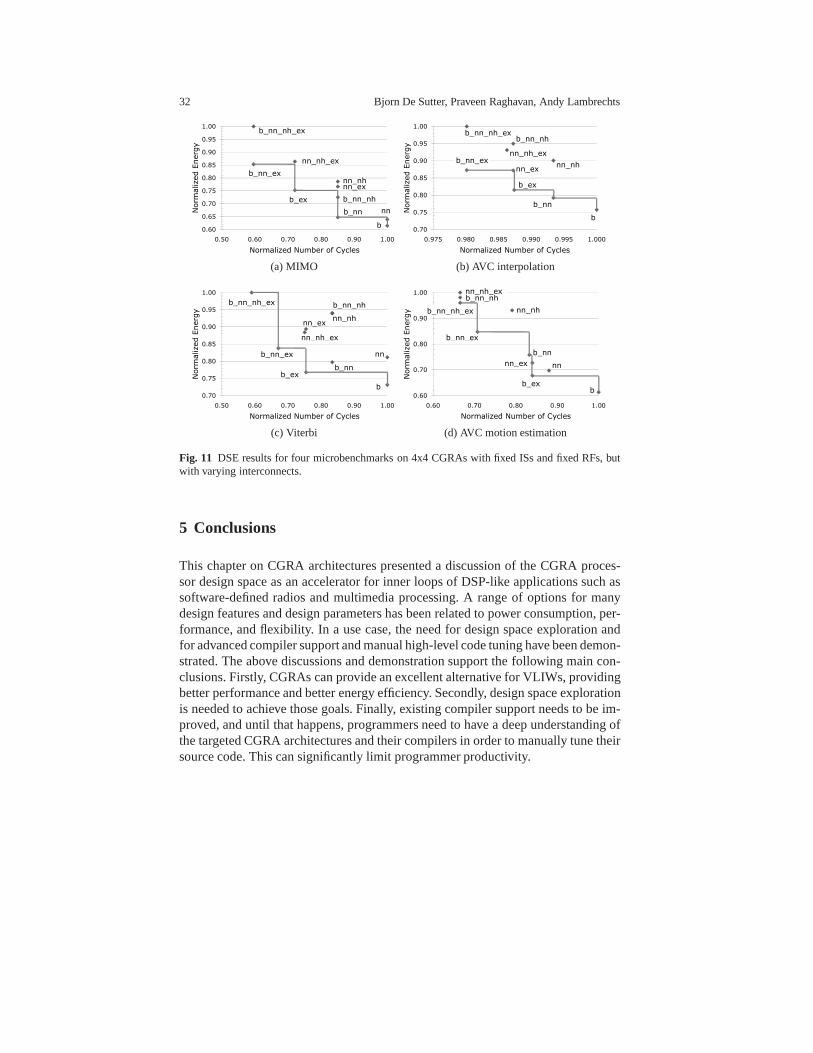
32 Bjorn De Sutter, Praveen Raghavan, Andy Lambrechts
(a) MIMO (b) AVC interpolation
(c) Viterbi (d) AVC motion estimation
Fig. 11 DSE results for four microbenchmarks on 4x4 CGRAs with fixed ISs and fixed RFs, butwith varying interconnects.
5 Conclusions
This chapter on CGRA architectures presented a discussion of the CGRA proces-sor design space as an accelerator for inner loops of DSP-like applications such assoftware-defined radios and multimedia processing. A rangeof options for manydesign features and design parameters has been related to power consumption, per-formance, and flexibility. In a use case, the need for design space exploration andfor advanced compiler support and manual high-level code tuning have been demon-strated. The above discussions and demonstration support the following main con-clusions. Firstly, CGRAs can provide an excellent alternative for VLIWs, providingbetter performance and better energy efficiency. Secondly,design space explorationis needed to achieve those goals. Finally, existing compiler support needs to be im-proved, and until that happens, programmers need to have a deep understanding ofthe targeted CGRA architectures and their compilers in order to manually tune theirsource code. This can significantly limit programmer productivity.

Coarse-Grained Reconfigurable Array Architectures 33
References
1. AHN, M., YOON, J. W., PAEK , Y., K IM , Y., K IEMB , M., AND CHOI, K. A spatial mappingalgorithm for heterogeneous coarse-grained reconfigurable architectures. InDATE ’06: Pro-ceedings of the conference on Design, automation and test inEurope(3001 Leuven, Belgium,Belgium, 2006), European Design and Automation Association, pp. 363–368.
2. BARUA , R. Maps: a compiler-managed memory system for software-exposed architectures.PhD thesis, Massachusetss Institute of Technology, January 2000.
3. BETZ, V., ROSE, J., AND MARGUARDT, A. Architecture and CAD for Deep-SubmicronFPGAs. Kluwer Academic Publishers, 1999.
4. BONDALAPATI , K. Parallelizing DSP nested loops on reconfigurable architectures using datacontext switching. InDAC ’01: Proceedings of the 38th annual Design Automation Confer-ence(New York, NY, USA, 2001), ACM, pp. 273–276.
5. BOUGARD, B., DE SUTTER, B., RABOU, S., NOVO, D., ALLAM , O., DUPONT, S., AND
VAN DER PERRE, L. A coarse-grained array based baseband processor for 100mbps+ soft-ware defined radio. InDATE ’08: Proceedings of the conference on Design, automation andtest in Europe(New York, NY, USA, 2008), ACM, pp. 716–721.
6. BOUGARD, B., DE SUTTER, B., VERKEST, D., VAN DER PERRE, L., AND LAUWEREINS,R. A coarse-grained array accelerator for software-definedradio baseband processing.IEEEMicro 28, 4 (2008), 41–50.
7. BOUWENS, F., BEREKOVIC, M., GAYDADJIEV, G., AND DE SUTTER, B. Architectureenhancements for the ADRES coarse-grained reconfigurable array. InProc. of HiPEAC Conf.(2008).
8. BURNS, G., AND GRUIJTERS, P. Flexibility tradeoffs in SoC design for low-cost SDR.Pro-ceedings of SDR Forum Technical Conference(2003).
9. BURNS, G., GRUIJTERS, P., HUISKENS, J.,AND VAN WEL, A. Reconfigurable acceleratorsenabling efficient SDR for low cost consumer devices.Proceedings of SDR Forum TechnicalConference(2003).
10. CARDOSO, J. M. P.,AND WEINHARDT, M. XPP-VC: A C compiler with temporal partition-ing for the PACT-XPP architecture. InFPL ’02: Proceedings of the Reconfigurable Comput-ing Is Going Mainstream, 12th International Conference on Field-Programmable Logic andApplications(London, UK, 2002), Springer-Verlag, pp. 864–874.
11. CERVERO, T., KANSTEIN, A., LOPEZ, S., DE SUTTER, B., SARMIENTO, R.,AND M IGNO-LET, J.-Y. Architectural exploration of the H.264/AVC decoderonto a coarse-grain recon-figurable architecture. InProc. of the International Conference on Design of CircuitsandIntegrated Systems(2008).
12. COONS, K. E., CHEN, X., BURGER, D., MCK INLEY, K. S., AND KUSHWAHA, S. K. Aspatial path scheduling algorithm for edge architectures.SIGPLAN Not. 41, 11 (2006), 129–140.
13. CORPORAAL, H. Microprocessor Architectures from VLIW to TTA. John Wiley, 1998.14. CRONQUIST, D., FRANKLIN , P., FISHER, C., FIGUEROA, M., AND EBELING, C. Architec-
ture design of reconfigurable pipelined datapaths. InProceedings of the Twentieth AnniversaryConference on Advanced Research in VLSI(1999).
15. DE SUTTER, B., COENE, P., VANDER AA , T., AND MEI, B. Placement-and-routing-basedregister allocation for coarse-grained reconfigurable arrays. InLCTES ’08: Proceedings of the2008 ACM SIGPLAN-SIGBED conference on Languages, compilers, and tools for embeddedsystems(New York, NY, USA, 2008), ACM, pp. 151–160.
16. DERUDDER, V., BOUGARD, B., COUVREUR, A., DEWILDE, A., DUPONT, S., FOLENS, L.,HOLLEVOET, L., NAESSENS, F., NOVO, D., RAGHAVAN , P., SCHUSTER, T., STINKENS,K., WEIJERS, J.-W.,AND DER PERRE, L. V. A 200Mbps+ 2.14nJ/b digital baseband multiprocessor system-on-chip for SDRs. InProc of VLSI Symposum(June 2009).
17. EBELING, C. Compiling for coarse-grained adaptable architectures. Tech. Rep. UW-CSE-02-06-01, University of Washington, 2002.

34 Bjorn De Sutter, Praveen Raghavan, Andy Lambrechts
18. EBELING, C. The general RaPiD architecture description. Tech. Rep.UW-CSE-02-06-02,University of Washington, 2002.
19. FISHER, J., FARABOSCHI, P.,AND YOUNG, C. Embedded Computing, A VLIW Approach toArchitecture, Compilers and Tools. Morgan Kaufmann, 2005.
20. FRIEDMAN , S., CARROLL, A., VAN ESSEN, B., YLVISAKER , B., EBELING, C., AND
HAUCK , S. SPR: an architecture-adaptive CGRA mapping tool. InFPGA ’09: Proceed-ing of the ACM/SIGDA international symposium on Field programmable gate arrays(NewYork, NY, USA, 2009), ACM, pp. 191–200.
21. GALANIS , M. D., MILIDONIS , A., THEODORIDIS, G., SOUDRIS, D., AND GOUTIS, C. E.A method for partitioning applications in hybrid reconfigurable architectures.Design Automa-tion for Embedded Systems 10, 1 (2006), 27–47.
22. GALANIS , M. D., THEODORIDIS, G., TRAGOUDAS, S., AND GOUTIS, C. E. A recon-figurable coarse-grain data-path for accelerating computational intensive kernels.Journal ofCircuits, Systems and Computers (JCSC)(2005), 877–893.
23. GEBHART, M., MAHER, B. A., COONS, K. E., DIAMOND , J., GRATZ, P., MARINO,M., RANGANATHAN , N., ROBATMILI , B., SMITH , A., BURRILL , J., KECKLER, S. W.,BURGER, D., AND MCK INLEY, K. S. An evaluation of the trips computer system. InAS-PLOS ’09: Proceeding of the 14th international conference on Architectural support for pro-gramming languages and operating systems(New York, NY, USA, 2009), ACM, pp. 1–12.
24. HARTENSTEIN, R., HERZ, M., HOFFMANN, T., AND NAGELDINGER, U. Mapping appli-cations onto reconfigurable kressarrays. InProceedings of the 9th International Workshop onField Programmable Logic and Applications(1999).
25. HARTENSTEIN, R., HERZ, M., HOFFMANN, T., AND NAGELDINGER, U. Generation ofdesign suggestions for coarse-grain reconfigurable architectures. InProceedings of the 10thInternational Workshop on Field Programmable Logic and Applications(2000).
26. HARTENSTEIN, R., HOFFMANN, T., AND NAGELDINGER, U. Design-space exploration oflow power coarse grained reconfigurable datapath array architectures. InProceedings of theInternational Workshop - Power and Timing Modeling, Optimization and Simulation(2000).
27. KIM , Y., K IEMB , M., PARK , C., JUNG, J.,AND CHOI, K. Resource sharing and pipeliningin coarse-grained reconfigurable architecture for domain-specific optimization. InDATE ’05:Proceedings of the conference on Design, Automation and Test in Europe(Washington, DC,USA, 2005), IEEE Computer Society, pp. 12–17.
28. KIM , Y., AND MAHAPATRA , R. A new array fabric for coarse-grained reconfigurable archi-tecture. InProceedings of the IEEE EuroMicro Conference on Digital System Design(2008),pp. 584–591.
29. KIM , Y., AND MAHAPATRA , R. Dynamic context compression for low-power coarse-grainedreconfigurable architecture.IEEE Transactions on Very Large Scale Integration (VLSI) Sys-tems(2009). To appear.
30. KIM , Y., MAHAPATRA , R., PARK , I., AND CHOI, K. Low power reconfiguration techniquefor coarse-grained reconfigurable architecture.IEEE Transactions on Very Large Scale Inte-gration (VLSI) Systems 17, 5 (2009), 593–603.
31. LAM , M. S. Software pipelining: an effecive scheduling technique for VLIW machines. InProc. PLDI (1988), pp. 318–327.
32. LAMBRECHTS, A., RAGHAVAN , P., JAYAPALA , M., CATTHOOR, F., AND VERKEST, D.Energy-aware interconnect optimization for a coarse grained reconfigurable processor.VLSIDesign, International Conference on 0(2008), 201–207.
33. LEE, J.-E., CHOI, K., AND DUTT, N. D. An algorithm for mapping loops onto coarse-grained reconfigurable architectures. InLCTES ’03: Proceedings of the 2003 ACM SIGPLANconference on Language, compiler, and tool for embedded systems(New York, NY, USA,2003), ACM, pp. 183–188.
34. LEE, L. H., MOYER, B., AND ARENDS, J. Instruction fetch energy reduction using loopcaches for embedded applications with small tight loops. InISLPED ’99: Proceedings of the1999 international symposium on Low power electronics and design(New York, NY, USA,1999), ACM, pp. 267–269.

Coarse-Grained Reconfigurable Array Architectures 35
35. LEE, M.-H., SINGH, H., LU, G., BAGHERZADEH, N., KURDAHI , F. J., FILHO , E. M. C.,AND ALVES, V. C. Design and implementation of the MorphoSys reconfigurable computingprocessor.J. VLSI Signal Process. Syst. 24, 2/3 (2000), 147–164.
36. MAHLKE , S. A., LIN , D. C., CHEN, W. Y., HANK , R. E.,AND BRINGMANN , R. A. Effec-tive compiler support for predicated execution using the hyperblock. InMICRO 25: Proceed-ings of the 25th annual international symposium on Microarchitecture (Los Alamitos, CA,USA, 1992), IEEE Computer Society Press, pp. 45–54.
37. MEI, B., DE SUTTER, B., VANDER AA , T., WOUTERS, M., KANSTEIN, A., AND DUPONT,S. Implementation of a coarse-grained reconfigurable mediaprocessor for AVC decoder.Journal of Signal Processing Systems 51, 3 (2008), 225–243.
38. MEI, B., LAMBRECHTS, A., VERKEST, D., MIGNOLET, J.-Y.,AND LAUWEREINS, R. Ar-chitecture exploration for a reconfigurable architecture template. IEEE Design and Test ofComputers 22, 2 (2005), 90–101.
39. MEI, B., VERNALDE, S., VERKEST, D., AND LAUWEREINS, R. Design methodology for atightly coupled VLIW/reconfigurable matrix architecture:A case study. InProc. of Design,Automation and Test in Europe (DATE)(2004), pp. 1224–1229.
40. MEI, B., VERNALDE, S., VERKEST, D., MAN , H. D., AND LAUWEREINS, R. ADRES: Anarchitecture with tightly coupled VLIW processor and coarse-grained reconfigurable matrix.In Proc. of Field-Programmable Logic and Applications(2003), pp. 61–70.
41. MEI, B., VERNALDE, S., VERKEST, D., MAN , H. D., AND LAUWEREINS, R. Exploitingloop-level parallelism for coarse-grained reconfigurablearchitecture using modulo schedul-ing. IEE Proceedings: Computer and Digital Techniques 150, 5 (2003).
42. NOVO, D., SCHUSTER, T., BOUGARD, B., LAMBRECHTS, A., VAN DER PERRE, L., AND
CATTHOOR, F. Energy-performance exploration of a CGA-based SDR processor.Journal ofSignal Processing Systems(2008).
43. OH, T., EGGER, B., PARK , H., AND MAHLKE , S. Recurrence cycle aware modulo schedul-ing for coarse-grained reconfigurable architectures. InLCTES ’09: Proceedings of the 2009ACM SIGPLAN/SIGBED conference on Languages, compilers, and tools for embedded sys-tems(New York, NY, USA, 2009), ACM, pp. 21–30.
44. PACT XPP TECHNOLOGIES. XPP-III Processor Overview White Paper, 2006.45. PARK , H., FAN , K., KUDLUR, M., AND MAHLKE , S. Modulo graph embedding: Mapping
applications onto coarse-grained reconfigurable architectures. InCASES ’06: Proceedingsof the 2006 international conference on Compilers, architecture and synthesis for embeddedsystems(New York, NY, USA, 2006), ACM, pp. 136–146.
46. PARK , H., FAN , K., MAHLKE , S. A., OH, T., KIM , H., AND K IM , H.-S. Edge-centric mod-ulo scheduling for coarse-grained reconfigurable architectures. InPACT ’08: Proceedings ofthe 17th international conference on Parallel architectures and compilation techniques(NewYork, NY, USA, 2008), ACM, pp. 166–176.
47. PETKOV, N. Systolic Parallel Processing. North Holland Publishing, 1992.48. P.RAGHAVAN , A.LAMBRECHTS, M.JAYAPALA , F.CATTHOOR, D.VERKEST, AND CORPO-
RAAL , H. Very wide register: An asymmetric register file organization for low power embed-ded processors. InDATE ’07: Proceedings of the conference on Design, Automation and Testin Europe(2007).
49. RAU , B. R. Iterative modulo scheduling. Tech. rep., Hewlett-Packard Lab: HPL-94-115,1995.
50. RAU , B. R., LEE, M., TIRUMALAI , P. P.,AND SCHLANSKER, M. S. Register allocation forsoftware pipelined loops. InPLDI ’92: Proceedings of the ACM SIGPLAN 1992 conferenceon Programming language design and implementation(1992), pp. 283–299.
51. SANKARALINGAM , K., NAGARAJAN, R., LIU , H., KIM , C., HUH, J., BURGER, D., KECK-LER, S. W., AND MOORE, C. R. Exploiting ILP, TLP, and DLP with the polymorphousTRIPS architecture.SIGARCH Comput. Archit. News 31, 2 (2003), 422–433.
52. SCARPAZZA, D. P., RAGHAVAN , P., NOVO, D., CATTHOOR, F., AND VERKEST, D. Soft-ware simultaneous multi-threading, a technique to exploittask-level parallelism to improveinstruction- and data-level parallelism. InProceedings of the 16th International Workshop on

36 Bjorn De Sutter, Praveen Raghavan, Andy Lambrechts
Integrated Circuit and System Design. Power and Timing Modeling, Optimization and Simu-lation (PATMOS)(2006), pp. 107–116.
53. SCHLANSKER, M., MAHLKE , S.,AND JOHNSON, R. Control CPR: a branch height reduc-tion optimization for EPIC architectures.SIGPLAN Not. 34, 5 (1999), 155–168.
54. SHEN, J., AND L IPASTI, M. Modern Processor Design: Fundamentals of Superscalar Pro-cessors. McGraw-Hill, 2005.
55. SILICON HIVE. HiveCC Databrief, 2006.56. SUDARSANAM, A. Code optimization libraries for retargetable compilationfor embedded
digital signal processors. PhD thesis, Princeton University, 1998.57. TAYLOR , M., K IM , J., MILLER , J., WENTZLA , D., GHODRAT, F., GREENWALD, B., HO,
H., LEE, M., JOHNSON, P., LEE, W., MA , A., SARAF, A., SENESKI, M., SHNIDMAN , N.,FRANK , V., AMARASINGHE, S., AND AGARWAL , A. The Raw microprocessor: A compu-tational fabric for software circuits and general purpose programs.IEEE Micro 22, 2 (2002),25–35.
58. TEXAS INSTRUMENTS. TMS320C64x Technical Overview, 2001.59. VAN BERKEL, K ., HEINLE, F. AMD MEUWISSEN, P., MOERMAN, K., AND WEISS, M.
Vector processing as an enabler for software-defined radio in handheld devices.EURASIPJournal on Applied Signal Processing 2005, 16 (2005), 2613–2625.
60. VAN DE WAERDT, J.-W., VASSILIADIS, S., DAS, S., MIROLO, S., YEN, C., ZHONG, B.,BASTO, C.,VAN ITEGEM, J.-P., AMIRTHARAJ, D., KALRA , K., RODRIGUEZ, P.,AND VAN
ANTWERPEN, H. The TM3270 media-processor. InMICRO 38: Proceedings of the 38thannual IEEE/ACM International Symposium on Microarchitecture (Washington, DC, USA,2005), IEEE Computer Society, pp. 331–342.
61. VENKATARAMANI , G., NAJJAR, W., KURDAHI , F., BAGHERZADEH, N., BOHM, W., AND
HAMMES, J. Automatic compilation to a coarse-grained reconfigurable system-on-chip.ACMTrans. Embed. Comput. Syst. 2, 4 (2003), 560–589.
62. WOH, M., L IN , Y., SEO, S., MAHLKE , S., MUDGE, T., CHAKRABARTI , C., BRUCE, R.,KERSHAW, D., REID, A., WILDER, M., AND FLAUTNER, K. From soda to scotch: Theevolution of a wireless baseband processor. InMICRO ’08: Proceedings of the 2008 41stIEEE/ACM International Symposium on Microarchitecture(Washington, DC, USA, 2008),IEEE Computer Society, pp. 152–163.
63. Programming XPP-III Processors White Paper, 2006.64. YOON, J., AHN, M., PAEK , Y., K IM , Y., AND K., C. Temporal mapping for loop pipelin-
ing on a MIMD-style coarse-grained reconfigurable architecture. InProc. International SoCDesign Conference(2006).

Index
accelerator, 6architecture for dynamically reconfigurable
embedded systems (ADRES), 20
coarse-grained reconfigurable array (CGRA), 2compiler optimization, 21
data dependence graph (DDG), 19data-level parallelism (DLP), 11design space exploration (DSE), 27
finite impulse response (FIR), 26
instruction-level parallelism (ILP), 2interconnects, 12, 30
kernel-only loops, 24
loop transformations, 22loop combination, 23loop fusion, 23
loop interchange, 23loop unrolling, 22
modulo routing resource graph (MRRG), 18modulo scheduling, 21multimedia processing, 27
Pareto, 31placement and routing, 18predication, 24
reconfigurable, 8routing, 18routing resource graph (RRG), 18
scheduling, 18single instruction multiple data (SIMD), 9, 12software pipelining, 21software-defined radio (SDR), 27
very long instruction word (VLIW), 4
37