coe3dj4 digital systems design - ece.mcmaster.cashirani/dd04/micro105.pdf– two 16 bit timers –...
TRANSCRIPT
CoE3DJ4Digital Systems Design
Hardware summary

Microprocessors vs. Microcontrollers • Microprocessors are single-chip CPU used in microcomputers• Microcontrollers and microprocessors are different in three
main aspects: hardware architecture, applications and instruction set features
• Hardware architecture: A microprocessor is a single chip CPU while microcontroller in a single IC contains a CPU and much of remaining circuitry of a complete computer (e.g., RAM, ROM, serial interface, parallel interface, timer, interrupt handling circuit)
• Applications: Microprocessors are commonly used as CPU in computers while microcontrollers are found in small, minimum component designs performing control oriented activates
Microprocessors vs. Microcontrollers• Instruction set:
– Microprocessor instruction sets are processing intensive. • Their instructions operate on nibbles, bytes, words, or even double words.• Addressing modes provide access to large arrays of data using pointers and
offsets– Microcontroller instruction sets cater to control of input and outputs.
• They have instructions to set and clear individual bits and perform bit operations
• Have instructions for input/output operations, event timing, enabling and setting priority levels for interrupts caused by external stimuli
• Processing power of a microcontroller is much less than a microprocessor

MCS-51• 8051 belongs to MCS-51 family of microcontrollers • MCS-51 was developed by Intel but other manufacturers (e.g.,
Siemens, Philips) are second source of this family. • Summary of features of 8051:
– 4K bytes ROM– 128 bytes RAM– Four 8-bit I/O ports– Two 16 bit timers– Serial interface– 64K external code memory space– 64K external data memory space– 210 bit-addressable locations
8051• 8051 has 40 pins• 32 pins function as I/O port lines, 24 of them are dual purpose
(each can operate as I/O or as a control line or part of addressor data bus)
• Eight lines in each port can be treated as a unit in interfacing to parallel devices (e.g, ADC) or each line can operate independently in interfacing to single bit devices (e.g., switches)
• Port 0: a dual purpose port on pins 32-39• Port 1: a dedicated I/O port on pins 1-8• Ports 2: dual purpose ports on pins 21-28 (could be a general
purpose I/O or high byte of the address bus for external memory)
• Ports 3: dual purpose ports on pins 10-17

MCS-51 Variants
• The 8031 requires external instruction memory.– It can be as large as 64K Bytes.– You lose 2 ports for interfacing to the external memory.
• You can replace these by interfacing the chip to an I/O port controller like the 8255.
6
1
2
2
128
0K
8031
8
1
4
3
256
8K
8052 8032875287518051Feature
EPROM
8
1
4
3
256
8k
8
1
2
3
256
0K
6
1
4
2
128
4k
6Interrupt Sources
1Serial Port
4I/O Ports
2Timers
128RAM (Bytes)
4KOn-Chip ROM

8051• /PSEN (Program Store Enable): is a control signal that
enables external code memory • It is usually connected to the output enable (/OE) pin of the
external code memory (e.g., EPROM)• When executing a program from internal ROM, /PSEN
remains in the inactive (high) state• ALE (Address Latch Enable): 8051 uses ALE for
demultiplexing the address and data bus• ALE pulses at 1/6th the on chip oscillator • When Port 0 is used in its alternate mode, ALE latches the
address into an external register during first half of memory cycle
• After this, Port 0 lines are available for data input or output during the second half of memory cycle
8051• /EA (external access, pin 31): if high, 8051 executes programs
from internal ROM. If low programs executes from external memory only
• RST (reset, pin 9): master reset for 8051. When high for two clock cycles, 8051 internal registers are loaded with appropriate values for a start-up
• On-chip oscillator inputs: 8051 oscillator is typically driven by a crystal connected to pins 18 and 19
• Nominal frequency: 12 MHz

Memory • 8051 implements a separate memory space for programs
(code) and data• Both code and data may be internal however both expand
using external components to a maximum of 64K code memory and 64K data memory
• Internal memory consists of on-chip ROM and on-chip data RAM.

Memory • On-chip RAM contains a rich arrangement of general purpose
storage, bit addressable storage, register banks, and special function register
• In 8051 the register and input output ports are memory mapped and accessible like any other memory location
• In 8051 stack resides within the internal RAM, rather than in external RAM
Memory-mapped• Some systems allow “memory-mapped” I/O where the I/O
devices are treated like memory locations.– The processor would use memory access instructions to access these
devices.
– I/O devices and memory locations cannot have the same address
• Therefore, we lose memory area when we use memory-mapped I/O.

Memory• Besides addresses 30H to 7FH, the bottom 32 bytes from 00H
to 2FH can be used as general purpose RAM.• Example: to read the content of internal RAM address 5FH
into accumulator: MOV A,5FH• Another way of doing the same thing:
MOV R0, #5FHMOV A, @R0

Bit addressable RAM• Individual accessing of bits is a powerful feature of
microcontrollers• Bits can be set, cleared, ANDed, ORed etc, with a single
instruction• 8051 ports are bit-addressable simplifying interface to single
bit inputs and outputs.• 8051 contains 210 bit-addressable locations• 128 of these locations are at addresses 20H to 2FH and the
rest are in the special function registers
Bit addressable RAM• These address can be accessed as byte or as bit depending on
the instruction• Example: SETB 67H
– Sets bit with address 67H which is the MSB of byte address 2CH
• What instruction can be used to set bit 3 in byte address 25H?– SETB 2BH
Register Banks• Bottom 32 locations of internal memory contains the register
banks• 8051 supports 8 registers R0 to R7 and after a system reset
(default) the registers are at address 00H to 07H• MOV A, R5: reads the content of address 05H into
accumulator• MOV A,05H with do the same thing• Active register bank may be altered by changing the register
bank select bits

Register Banks• Assuming register bank 3 is active, the following instruction
write contents of accumulator into location 18H:– MOV R0,A
• Idea of register bank permits fast and effective context switching
• Example: what is the address of register R5 in register bank 3?– 1DH
Special function registers• 8051 has 21 special function registers (SFRs) at the top of
internal RAM from address 80H to FFH.• Most of addresses from 80H to FFH are not defined except 21
of them.• Some SFRs are both bit-addressable and byte addressable and
it depends on the instruction• Example: What instruction can set MSB of accumulator B?
– SETB F7H

The ACC – Accumulator• Commonly used for move and arithmetic instructions.• Can be referred to in several ways:
– Implicitly in opcodes. – Referred to as ACC (or A) for instructions that allow specifying a register.– By its SFR address 0E0H.
• Bit addressable.– ACC.2 means bit 2 of the ACC register.

The B Register• Commonly used as a temporary register, much like a 9th R
register.• B register or accumulator B at address F0H is used along with
the accumulator for multiply and divide operations • MUL AB: multiplies 8 bit unsigned values in A and B and
leaves the 16 bit result in A (low byte) and B (high byte)• DIV AB: divided A by B, leaving the integer result in A and
remainder in B• B register is bit-addressable• Can also be accessed through its SFR address of 0F0H.
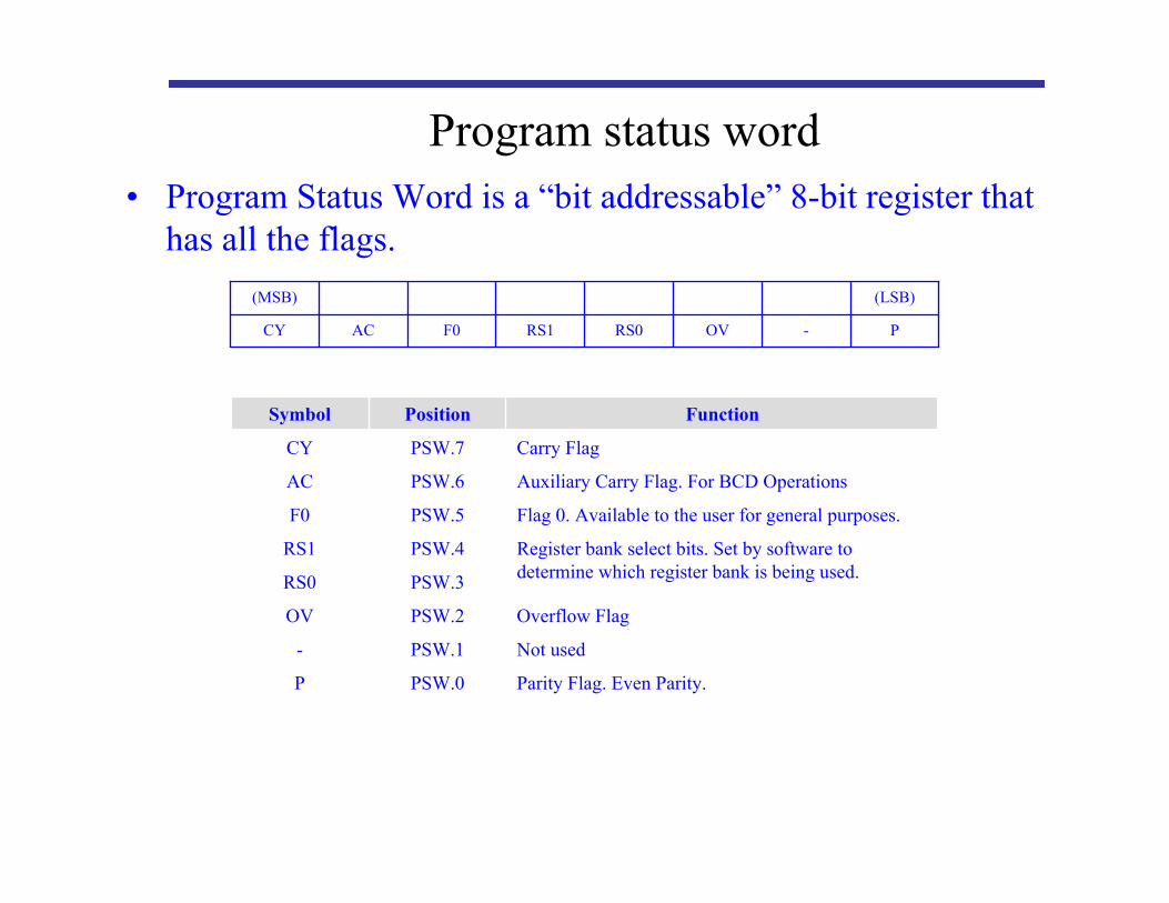
Program status word• Program Status Word is a “bit addressable” 8-bit register that
has all the flags.
P-OVRS0RS1F0ACCY
(LSB)(MSB)
Parity Flag. Even Parity.PSW.0P
Not usedPSW.1-
Overflow FlagPSW.2OV
PSW.3RS0
Register bank select bits. Set by software to determine which register bank is being used.
PSW.4RS1
Flag 0. Available to the user for general purposes.PSW.5F0
Auxiliary Carry Flag. For BCD OperationsPSW.6AC
Carry FlagPSW.7CY
FunctionPositionSymbol
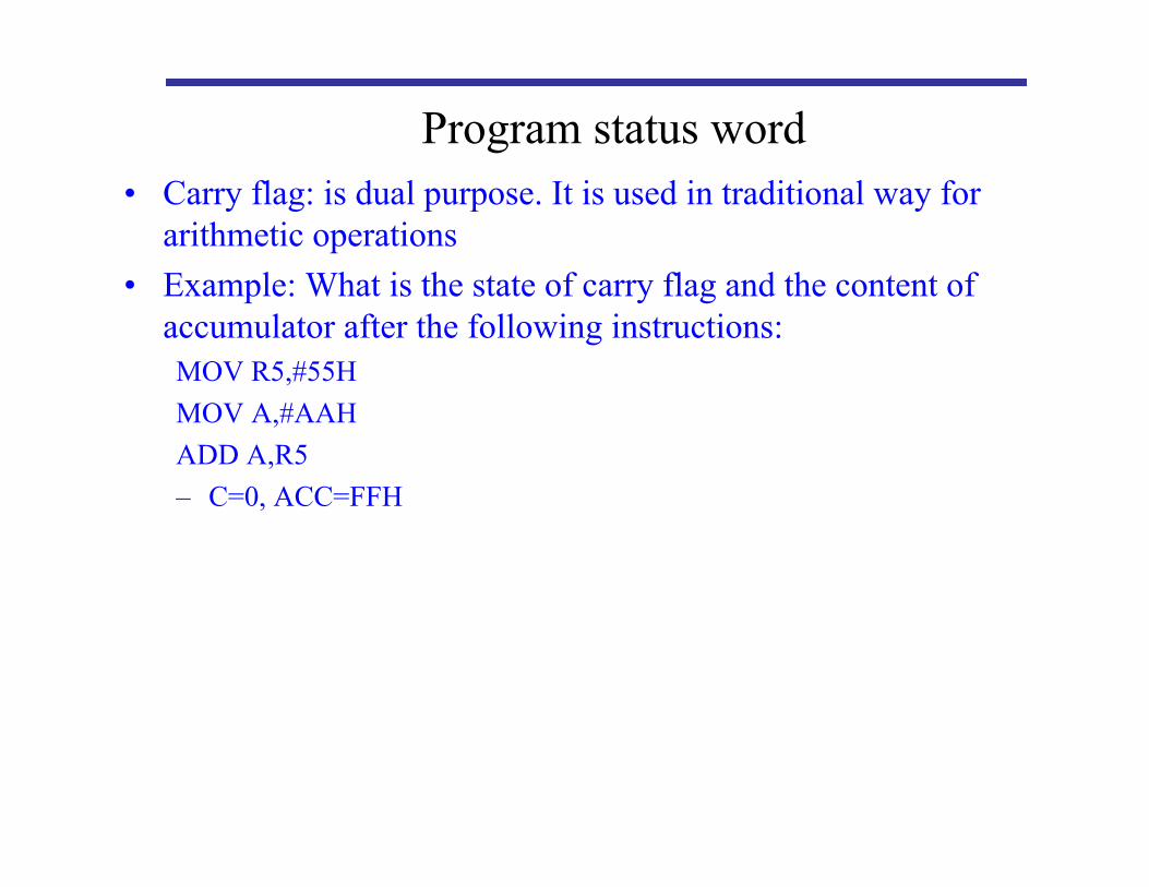
Program status word• Carry flag: is dual purpose. It is used in traditional way for
arithmetic operations• Example: What is the state of carry flag and the content of
accumulator after the following instructions:MOV R5,#55HMOV A,#AAHADD A,R5– C=0, ACC=FFH

Program status word• Carry flag is also the “Boolean accumulator”: 1 bit register for
Boolean instructions• Example: ANLC,25H• ANDs bit 25H with the carry flag and places the result back in
carry flag
• Auxiliary carry flag (AC): is set if a carry was generated out of bit 3 into bit 4 or if the result in the lower nibble is in the range 0AH to 0FH
• AC is useful in arithmetic operations on binary coded decimal (BCD) values.

Program status word• Example: what is AC and the content of accumulator after the
following sequence of instructions: MOV R5,#1MOV A,#9ADD A,R5
• Answer: AC=1, ACC=0AH• Flag 0 (F0): a general purpose flag bit available for user • Register Bank Select Bits (RS0 and RS1): determine the
active register bank • Example: the following instructions enable register bank 3
and move the content of R7 (address 1FH) to accumulator SETB RS1SETB RS0MOV A,R7
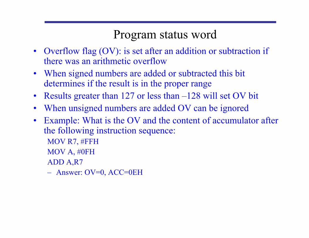
Program status word• Overflow flag (OV): is set after an addition or subtraction if
there was an arithmetic overflow• When signed numbers are added or subtracted this bit
determines if the result is in the proper range• Results greater than 127 or less than –128 will set OV bit• When unsigned numbers are added OV can be ignored• Example: What is the OV and the content of accumulator after
the following instruction sequence:MOV R7, #FFHMOV A, #0FHADD A,R7– Answer: OV=0, ACC=0EH

Program status word• Parity bit (p): is automatically set or cleared in each machine
cycle to establish even parity in the accumulator• Number of 1-bits in the accumulator plus P is always even • P is used in serial port routines • What is the state of P after execution of the following
instruction?MOV A,#55H– Answer: P=0

Stack pointer• Stack pointer (SP) is an 8-bit register at address 81H• It contains the address of the data item currently on top of the
stack.• Stack operations include pushing data on the stack and
popping data off the stack• Pushing increments SP before writing the data• Popping from the stack reads the data and decrements the SP• 8051 stack is kept in the internal RAM• Depending on the initial value of the SP, stack can have
different sizes• Example: MOV SP,#5FH• On 8051 this would limit the stack to 32 bytes since the
uppermost address of on chip RAM is 7FH.

Stack pointer• The default value of SP (after system reset) is 07H.• This result in the first stack write operation to store data in
location 08H which means that register bank 1 (and possible 2 and 3) are not available
• User may initialize the SP to avoid this
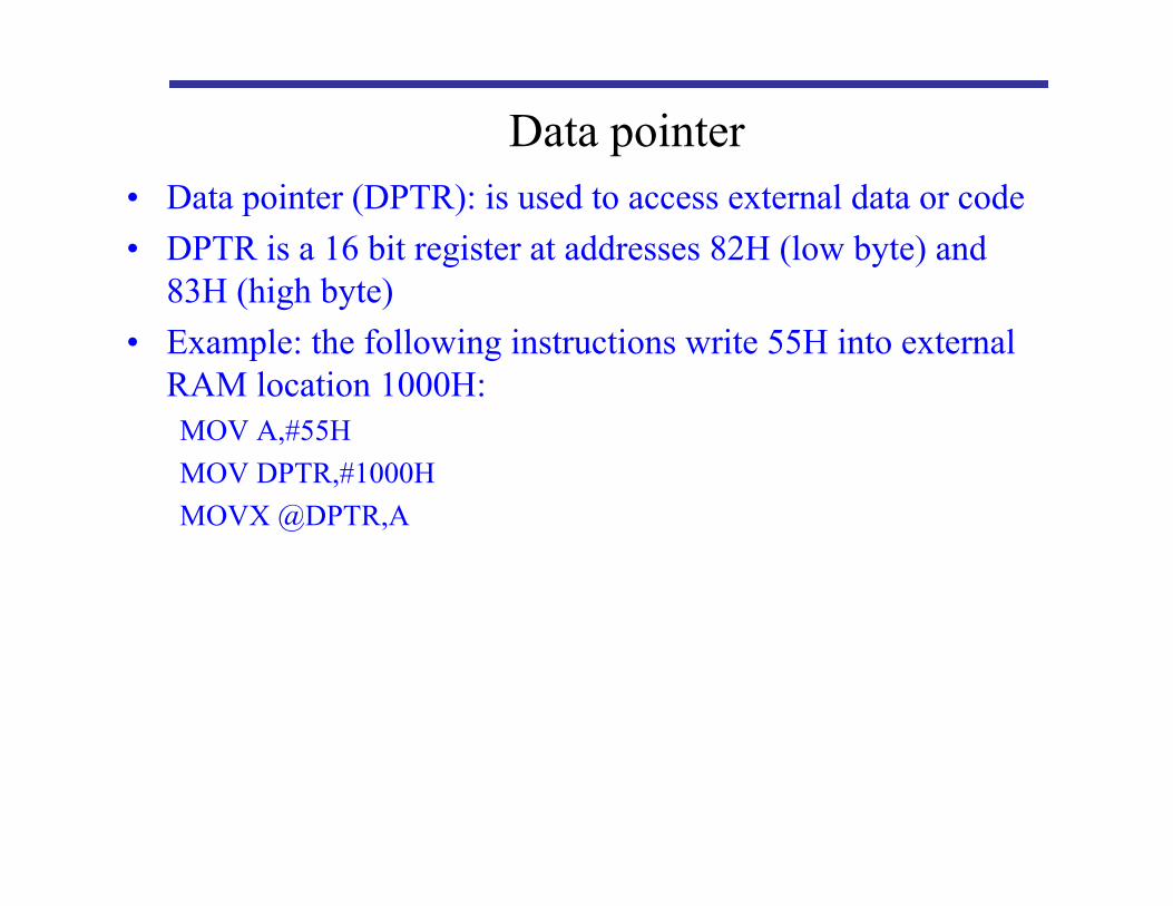
Data pointer • Data pointer (DPTR): is used to access external data or code• DPTR is a 16 bit register at addresses 82H (low byte) and
83H (high byte)• Example: the following instructions write 55H into external
RAM location 1000H:MOV A,#55HMOV DPTR,#1000HMOVX @DPTR,A
Port registers• 8051 I/O ports consists of Port 0 at address 80H, port 1 at
address 90H, Port 2 at address A0H and port 3 at address B0H.
• Ports 0,2 and 3 may not be available for I/O if external memory is used or if some of the 8051 special features are used
• Ports P1 is always available for general purpose I/O• All ports are bit addressable, providing powerful interfacing
possibilities • Example: a motor which is connected to port 1 bit 7 through a
transistor driver can be turned on and off using the following 8051 instructions:SETB P1.7CLR P1.7

Timer registers• 8051 contains two 16 bit timer/counter for timing intervals
and counting events• Timer 0 is at addresses 8AH (TL0, low byte) and 8CH (TH0
high byte)• Timer 1 is at addresses 8BH (TL1, low byte) and 8DH (TH1
high byte)• Timer operation is set by the timer mode register (TMOD) at
address 89H and timer control register (TCON) at address 88H

Serial port registers• Serial port register: 8051 contains an on-chip serial port for
communicating with serial devices • One register, the serial data buffer (SBUF) at address 90H,
hold both transmitted data and received data• Writing to SBUF loads data for transmission• Reading SBUF accesses received data• Various modes of operation can be programmed through bit
addressable serial port control register (SCON) at address 98H

Interrupt registers• 8051 has a 5-source, 2 priority level interrupt structure• Interrupts are disabled after a system reset and then enabled
by writing to the interrupt enable register (IE) at address A8H• Priority level is set through interrupt priority register (IP) at
address B8H.
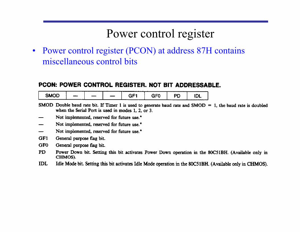
Power control register• Power control register (PCON) at address 87H contains
miscellaneous control bits

Power control register• SMOD bit doubles the serial port baud rate when in Modes 1,
2, 3• PCON bits 6,5, and 4 are undefined• Bits 3 and 2 are general purpose flag bits available for user
Power control register• For power critical applications 8051 provides power reduced
modes: Idle and Power-down• Idle mode: An instruction that sets the IDL bit will be the last
instruction executed before entering idle mode• In idle mode the internal clock is gated off to the CPU but not
to the interrupt, timer and serial port functions. • CPU stops executing instructions• All register and on-chip RAM contents are maintained • Idle mode is terminated by any interrupt or by a system reset

Power control register• Power down mode (PD): An instruction that sets the PD bit
will be the last instruction executed before entering power down mode
• In power down mode:– the on-chip oscillator is stopped – all on chip RAM and SFRs contents are retained – port pins retain their logic levels
• Power-down mode can be terminated by external interrupts or reset

External memory• Microcontrollers should have expansion capabilities• MCS-51 provides this in the form of 64K external code
memory space and a 64K external data memory space• When external memory is used Port 0 becomes a multiplexed
address (A0-A7) and data (D0-D7) bus with ALE latching the low-byte of the address at the beginning of each external memory cycle
• Port 2 is employed for the high-byte of the address bus
External memory• External code memory is read only memory and is enabled by
the /PSEN signal• An 8051 machine cycle is 12 oscillator periods• During a typical machine cycle, ALE pulses twice and 2 bytes
are read from program memory
External memory• External data memory is read/write memory enabled by RD
and WR (P3.7 and P3.6)• RD is connected to OE of the external RAM and WE is
connected to RAM’s W line. • The only access to external data memory is with MOVX
instruction, using either 16 bit data pointer (DPTR), R0 or R1 as the address register