commell mpx24794g2 programmer's manual
TRANSCRIPT

Commell MPX24794G2 Programmer’s Manaul
Taiwan Commate Computer Inc. 1
Commell MPX24794G2 Programmer’s Manual Version 1.0.1.0

Commell MPX24794G2 Programmer’s Manaul
Taiwan Commate Computer Inc. 2
Contents 1 Hardware..................................................................................................................... 4
1.1 Cypress CY8C24794 .......................................................................................... 5 1.2 Signaling ............................................................................................................. 5
1.2.1 CN_GPIO1.................................................................................................. 7 1.2.2 CN_GPIO2.................................................................................................. 8 1.2.3 CN_J1 ......................................................................................................... 8 1.2.4 CN_USB ..................................................................................................... 8 1.2.5 MINI-PCIe .................................................................................................. 9
1.3 Cables.................................................................................................................. 9 1.3.1 OALUSB-H4 .............................................................................................. 9 1.3.2 OALUSB-H4-1 ......................................................................................... 10 1.3.3 OAL-24794S-ADP ................................................................................... 11 1.3.4 OAL-24794S-CN1.................................................................................... 12 1.3.5 OAL-24794S-CN2.................................................................................... 13
1.4 General Purpose Input Output .......................................................................... 14 1.4.1 Digital IO .................................................................................................. 15 1.4.2 Mapping .................................................................................................... 15
1.5 Drive Mode ....................................................................................................... 16 1.6 PRTxDMx Registers......................................................................................... 18 1.7 Configuring I/O................................................................................................. 19 1.8 Read/Modify/Write Considerations .................................................................. 21
1.8.1 The Simple Cases...................................................................................... 22 1.8.2 Shared Outputs and Complex Mode Inputs .............................................. 22 1.8.3 Shadow Registers Solution ....................................................................... 23 1.8.4 Using Complex Drive Modes ................................................................... 24 1.8.5 Reset State and Configuration .................................................................. 24
1.9 Default Pin State ............................................................................................... 25 2 Firmware Guide ........................................................................................................ 26
2.1 USB Characteristics .......................................................................................... 26 2.2 System Tick Count............................................................................................ 27 2.3 Common Communication Protocol .................................................................. 27
2.3.1 Protocol ..................................................................................................... 28 2.3.2 Bulk Packet Format................................................................................... 29 2.3.3 Interrupt Packet Format ............................................................................ 29 2.3.4 MPX24794G2 Commands........................................................................ 30
2.3.4.1 CCP_CMND_SYS_GET_SYSTEM_INFO......................................... 31 2.3.4.2 CCP_CMND_SYS_GET_TICK_COUNT........................................... 32 2.3.4.3 CCP_CMND_SYS_READ_REGISTERS ........................................... 33 2.3.4.4 CCP_CMND_SYS_WRITE_REGISTERS.......................................... 34 2.3.4.5 CCP_CMND_GPIO_READ_REGISTERS ......................................... 35 2.3.4.6 CCP_CMND_GPIO_WRITE_REGISTERS........................................ 36
3 Software Guide ......................................................................................................... 37 3.1 Device Drivers Guide ....................................................................................... 37
3.1.1 Device Drivers Organization .................................................................... 37 3.1.2 Windows 2000 .......................................................................................... 37
Commell MPX24794G2 Programmer’s Manaul
Taiwan Commate Computer Inc. 3
3.1.3 Windows XP (32-bit) Device Driver ........................................................ 38 3.1.4 Windows XP (64-bit) Device Driver ........................................................ 38 3.1.5 Windows Vista (32-bit) and Windows 7 (32-bit) Device Driver ............. 39 3.1.6 Windows Vista (64-bit) and Windows 7 (64-bit) Device Driver ............. 39 3.1.7 GUID......................................................................................................... 40
3.2 How to Install Device Driver............................................................................ 40 3.3 Cypress CyUSB ................................................................................................ 40
3.3.1 CyConsole................................................................................................. 41 3.3.2 CyAPI ....................................................................................................... 44 3.3.3 CyUSB.NET ............................................................................................. 44
3.4 Programming Guide.......................................................................................... 44 3.4.1 MPX-24794G2 Common Communication Protocol ................................ 44 3.4.2 Shadow Register Programming ................................................................ 45 3.4.3 C/C++ Programming................................................................................. 46 3.4.4 .NET Class Library ................................................................................... 46
4 MPX24794G2 SDK for Windows ............................................................................ 48 4.1 File Organization .............................................................................................. 48 4.2 Files................................................................................................................... 48 4.3 Project Example ................................................................................................ 49 4.4 Sample Codes.................................................................................................... 50
5 API Reference........................................................................................................... 53 5.1 CCP_Open ........................................................................................................ 54 5.2 CCP_GetSerialNumber..................................................................................... 55 5.3 CCP_Close........................................................................................................ 56 5.4 CCP_SetWaitTime............................................................................................ 57 5.5 SYSTEM_GetSystemInfo................................................................................. 58 5.6 SYSTEM_GetTickCount.................................................................................. 59 5.7 SYSTEM_ReadRegisters.................................................................................. 60 5.8 SYSTEM_WriteRegisters................................................................................. 61 5.9 GPIO_ReadPRTxDR ........................................................................................ 62 5.10 GPIO_WritePRTxDR ....................................................................................... 63 5.11 GPIO_ReadPRTxIE.......................................................................................... 64 5.12 GPIO_WritePRTxIE......................................................................................... 65 5.13 GPIO_ReadPRTxICx........................................................................................ 66 5.14 GPIO_WritePRTxICx....................................................................................... 67 5.15 GPIO_ReadPRTxDMx ..................................................................................... 68 5.16 GPIO_WritePRTxDMx .................................................................................... 69 5.17 GPIO_SetModePort .......................................................................................... 70 5.18 GPIO_SetModePin ........................................................................................... 71 5.19 GPIO_ReadPort ................................................................................................ 72 5.20 GPIO_WritePort ............................................................................................... 73 5.21 INT_ReadPacket ............................................................................................... 74
6 References................................................................................................................. 75

Commell MPX24794G2 Programmer’s Manaul
Taiwan Commate Computer Inc. 4
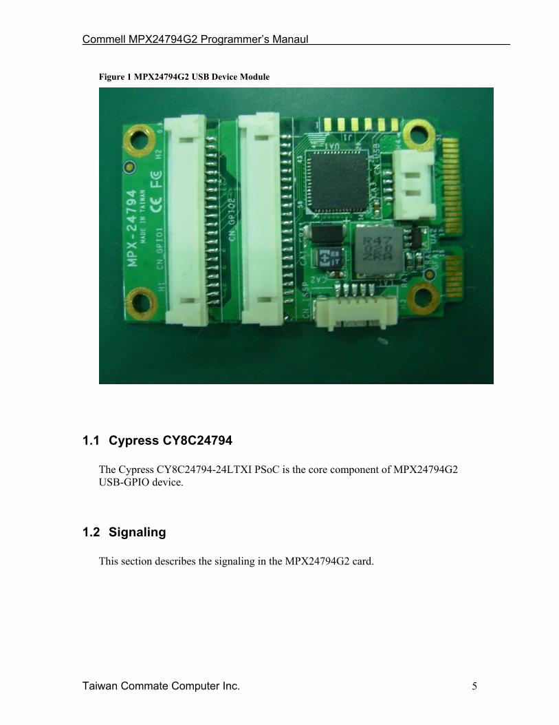
1 Hardware The MPX24794G2 USB-GPIO card is a USB 2.0 full speed compliant device, which implements 32 bits General Purpose Input/Output (GPIO) functions. Figure 1 depicts the MPX24794G2 USB-GPIO card. The MPX24794G2 USB-GPIO device adopts Cypress CY8C24794-24LTXI PSoC as the core component. The GPIO contains input buffers, output drivers, register bit storage, and configuration logic for connecting the PSoC device to the outside world. IO Ports are arranged with (up to) 8 bits per port. Each full port contains eight identical GPIO blocks, with connections to identify a unique address and register bit number for each block. Features
• USB 2.0 Full Speed compliant • 32-bit GPIO grouped into four 8-bit ports • Digital IO (digital input and output controlled by software) • Each IO pin also has up to 8 drive modes • Each port can be individually programmed to either Input or Output • Produced in Mini-PCIe card form factor (easily locked on motherboard)
Commell MPX24794G2 Programmer’s Manaul
Taiwan Commate Computer Inc. 5
Figure 1 MPX24794G2 USB Device Module
1.1 Cypress CY8C24794 The Cypress CY8C24794-24LTXI PSoC is the core component of MPX24794G2 USB-GPIO device.
1.2 Signaling This section describes the signaling in the MPX24794G2 card.

Commell MPX24794G2 Programmer’s Manaul
Taiwan Commate Computer Inc. 6
Figure 2 MPX24794G2 Connectors
Number Name
1 CN_GPIO1 2 CN_GPIO2 3 CN_J1 4 MINI-PCIe card interface 5 CN_USB
Commell MPX24794G2 Programmer’s Manaul
Taiwan Commate Computer Inc. 7
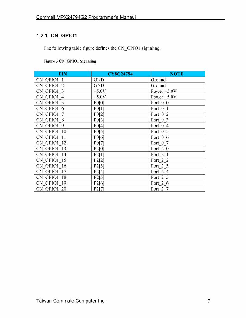
1.2.1 CN_GPIO1 The following table figure defines the CN_GPIO1 signaling. Figure 3 CN_GPIO1 Signaling
PIN CY8C24794 NOTE CN_GPIO1_1 GND Ground CN_GPIO1_2 GND Ground CN_GPIO1_3 +5.0V Power +5.0V CN_GPIO1_4 +5.0V Power +5.0V CN_GPIO1_5 P0[0] Port_0_0 CN_GPIO1_6 P0[1] Port_0_1 CN_GPIO1_7 P0[2] Port_0_2 CN_GPIO1_8 P0[3] Port_0_3 CN_GPIO1_9 P0[4] Port_0_4 CN_GPIO1_10 P0[5] Port_0_5 CN_GPIO1_11 P0[6] Port_0_6 CN_GPIO1_12 P0[7] Port_0_7 CN_GPIO1_13 P2[0] Port_2_0 CN_GPIO1_14 P2[1] Port_2_1 CN_GPIO1_15 P2[2] Port_2_2 CN_GPIO1_16 P2[3] Port_2_3 CN_GPIO1_17 P2[4] Port_2_4 CN_GPIO1_18 P2[5] Port_2_5 CN_GPIO1_19 P2[6] Port_2_6 CN_GPIO1_20 P2[7] Port_2_7

Commell MPX24794G2 Programmer’s Manaul
Taiwan Commate Computer Inc. 8
1.2.2 CN_GPIO2 The following figure defines the CN_GPIO2 signaling.
Figure 4 CN_GPIO2 Signaling
1.2.3 CN_J1 CN_J1 is test pins connector.
1.2.4 CN_USB This connector is optional if the card is inserted into a Mini-PCIe slot.
Figure 5 CN_USB Signaling
Pin Name 1 +5V
PIN CY8C24794 NOTE CN_GPIO2_1 P3[0] Port_3_0 CN_GPIO2_2 P3[1] Port_3_1 CN_GPIO2_3 P3[2] Port_3_2 CN_GPIO2_4 P3[3] Port_3_3 CN_GPIO2_5 P3[4] Port_3_4 CN_GPIO2_6 P3[5] Port_3_5 CN_GPIO2_7 P3[6] Port_3_6 CN_GPIO2_8 P3[7] Port_3_7 CN_GPIO2_9 P4[0] Port_4_0 CN_GPIO2_10 P4[1] Port_4_1 CN_GPIO2_11 P4[2] Port_4_2 CN_GPIO2_12 P4[3] Port_4_3 CN_GPIO2_13 P4[4] Port_4_4 CN_GPIO2_14 P4[5] Port_4_5 CN_GPIO2_15 P4[6] Port_4_6 CN_GPIO2_16 P4[7] Port_4_7 CN_GPIO2_17 N/C Not connected CN_GPIO2_18 N/C Not connected CN_GPIO2_19 GND Ground CN_GPIO2_20 GND Ground

Commell MPX24794G2 Programmer’s Manaul
Taiwan Commate Computer Inc. 9
2 D- 3 D+ 4 GND
1.2.5 MINI-PCIe Please be noted that only the USB signaling is used in the Mini-PCIe card interface signal.
Figure 6 USB signaling of Mini-PCIe card signaling
Pin Name 36 USB_D- 38 USB_D+
4,9,1518, … GND 24,39,41 3.3Vaux
1.3 Cables This section describes how to cabling the MPX24794G2 card. Please be noted that all cables are optional. Choose one that fits your needs or make your own cables.
1.3.1 OALUSB-H4
Figure 7 OALUSB-H4 cable
OALUSB-H4 cable is designed to connect the MPX24794G2 card to a USB pin header on a motherboard instead of inserting into a Mini-PCIe slot.

Commell MPX24794G2 Programmer’s Manaul
Taiwan Commate Computer Inc. 10
Figure 8 OALUSB-H4 drawing
Please refer to the OALUSB-H4.PDF file in the CD for detail mechanical drawing and specification.
1.3.2 OALUSB-H4-1
Figure 9 OALUSB-H4-1 cable
This optional cable allows you to connect the MPX24794G2 card to a USB Type A receptacle instead of inserting in a Mini-PCIe slot on a motherboard.
Figure 10 OALUSB-H4-1 drawing

Commell MPX24794G2 Programmer’s Manaul
Taiwan Commate Computer Inc. 11
Please refer to the OALUSB-H4-1.PDF file in the CD for detail mechanical drawing and specification.
1.3.3 OAL-24794S-ADP
Figure 11 OAL-24794S-ADP cable
OAL-24794S-ADP cable is designed to connect MPX24794G / MPX24794G2 / MPX24794S card to Commell ADP-GPION4I4O5V or ADP-GPION8I5V signal isolation / convert cards. ADP-GPION4I4O5V supports 4x photo-couple inputs and 4x relay outputs. ADP-GPION8I5V supports 8x photo-couple inputs. Please visit http://www.commell.com.tw/Product/Peripheral/GPIO converter module/GPIO Convert Module.HTM
Figure 12 OAL-24794S-ADP drawing
Commell MPX24794G2 Programmer’s Manaul
Taiwan Commate Computer Inc. 12
Please refer to the OAL-24794S-ADP.PDF for the mechanical drawing and detail specification.
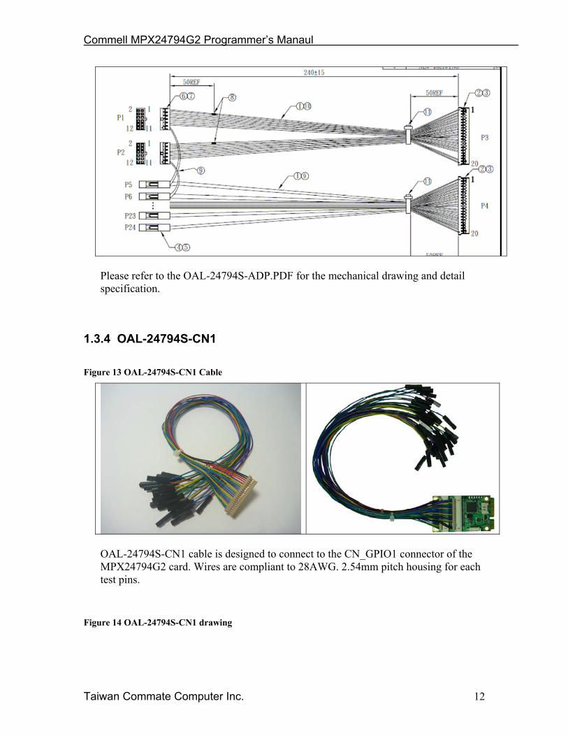
1.3.4 OAL-24794S-CN1
Figure 13 OAL-24794S-CN1 Cable
OAL-24794S-CN1 cable is designed to connect to the CN_GPIO1 connector of the MPX24794G2 card. Wires are compliant to 28AWG. 2.54mm pitch housing for each test pins.
Figure 14 OAL-24794S-CN1 drawing

Commell MPX24794G2 Programmer’s Manaul
Taiwan Commate Computer Inc. 13
Please refer to the OAL-24794S-CN1.PDF for detail mechanical drawing and more specifications.
1.3.5 OAL-24794S-CN2
Figure 15 OAL-24794S-CN2 cable
OAL-24794S-CN2 cable is designed to connect to the CN_GPIO2 connector of the MPX24794G2 card. Wires are compliant to 28AWG. 2.54mm pitch housing for each test pins are provided.
Figure 16 OAL-24794S2-CN2 drawing

Commell MPX24794G2 Programmer’s Manaul
Taiwan Commate Computer Inc. 14
Please refer to the OAL-24794S-CN2.PDF file in the CD for detail mechanical drawing and specification.
1.4 General Purpose Input Output The GPIO contains input buffers, output drivers, register bit storage, and configuration logic for connecting the PsoC device to the outside world. IO Ports are arranged with (up to) 8 bits per port. Each full port contains eight identical GPIO blocks, with connections to identify a unique address and register bit number for each block. MPX-24794G uses Port 0, Port 2, Port 3, and Port 4 to implement 32-pin programmable general purpose IO. Each IO pin also has up to seven drive modes that the user can program in order to meet the real world requirements. The following drive modes are supported for your programming.
1. Mode 0: Resistive pull down
2. Mode 1: Strong drive
3. Mode 2: High impedance
4. Mode 3: Resistive pull up
5. Mode 4: Open drain, drives high
6. Mode 5: Slow strong drive
7. Mode 6: High impedance analog
8. Mode 7: Open drain, drives low

Commell MPX24794G2 Programmer’s Manaul
Taiwan Commate Computer Inc. 15
1.4.1 Digital IO This section contains the text from the PSoC TRM, Document No. 001-14483 Rev. *F. Please refer to this manual for detail information. One of the basic operations of the GPIO ports is to allow the M8C to send information out of the PSoC device and get information into the M8C from outside the PSoC device. This is accomplished by way of the port data register (PRTxDR). Writes from the M8C to the PRTxDR register store the data state, one bit per GPIO. In the standard non-bypass mode, the pin drivers drive the pin in response to this data bit, with a drive strength determined by the Drive mode setting. The actual voltage on the pin depends on the Drive mode and the external load. The M8C can read the value of a port by reading the PRTxDR register address. When the M8C reads the PRTxDR register address, the current value of the pin voltage is translated into a logical value and returned to the M8C. Note that the pin voltage can represent a different logic value than the last value written to the PRTxDR register. This is an important distinction to remember in situations such as the use of a read modify write to a PRTxDR register. Examples of read modify write instructions include AND, OR, and XOR. The following is an example of how a read modify write, to a PRTxDR register, could have an unexpected and even indeterminate result in certain systems. Consider a scenario where all bits of Port 1 on the PSoC device are in the strong 1 resistive 0 drive mode; so that in some cases, the system the PSoC is in may pull up one of the bits. mov reg[PRT1DR], 0X00 or reg[PRT1DR], 0X80 In the first line of code above, writing a 0x00 to the port will not affect any bits that happen to be driven by the system the PSoC is in. However, in the second line of code, it can not guarantee that only bit 7 will be the one set to a strong 1. Because the OR instruction will first read the port, any bits that are in the pull up state will be read as a ‘1’. These ones will then be written back to the port. When this happens, the pin will go into a strong 1 state; therefore, if the pull up condition ends in the system, the PSoC will keep the pin value at a logic 1.
1.4.2 Mapping MPX-24794G maps the PRTxDR registers to the outside GPIO as the following table.
Table 1 PRTxDR/GPIO mapping

Commell MPX24794G2 Programmer’s Manaul
Taiwan Commate Computer Inc. 16
PRTxDR GPIO Description PRT0DR[7..0] GPIO[7..0] Each bit of the Port_0 is connecting to each
GPIO pin 7 to pin 0 correspondingly. PRT2DR[7..0] GPIO[15..8] Each bit of the Port_2 is connecting to each
GPIO pin 15 to pin 8 correspondingly. PRT3DR[7..0] GPIO[23..16] Each bit of the Port_3 is connecting to each
GPIO pin 23 to pin 16 correspondingly. PRT4DR[7..0] GPIO[31..24] Each bit of the Port_4 is connecting to each
GPIO pin 31 to pin 24 correspondingly. Please be noted that writes from the M8C to the PRTxDR register store the data state, one bit per GPIO. In the standard non-bypass mode, the pin drivers drive the pin in response to this data bit with a drive strength determined by the Drive mode setting (see Drive Mode section). The actual voltage on the pin depends on the Drive mode and the external load.
1.5 Drive Mode Please refer to “6.2.4 PRTxDMx Registers” (page 105) of the CY8C24x94 PSoC Technical Reference Manual” for detail information about the drive mode of GPIO ports.
Commell MPX24794G2 Programmer’s Manaul
Taiwan Commate Computer Inc. 17
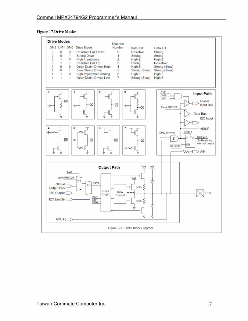
Figure 17 Drive Modes

Commell MPX24794G2 Programmer’s Manaul
Taiwan Commate Computer Inc. 18
1.6 PRTxDMx Registers
The Port Drive Mode Bit Registers (PRTxDMx) are used to specify the Drive mode for GPIO pins. Bits 7 to 0: Drive Mode x[7:0]. In the PRTxDMx registers there are eight possible drive modes for each port pin. Three mode bits are required to select one of these modes, and these three bits are spread into three different registers (PRTxDM0, PRTxDM1, and PRTxDM2). The bit position of the effected port pin (for example, Pin[2] in Port 0) is the same as the bit position of each of the three drive mode register bits that control the Drive mode for that pin (for example, bit[2] in PRT0DM0, bit[2] in PRT0DM1, and bit[2] in PRT0DM2). The three bits from the three registers are treated as a group. These are referred to as DM2, DM1, and DM0, or together as DM[2:0]. Drive modes are showed in the following table.
Table 2 Pin Drive Modes
For analog IO, the Drive mode should be set to one of the High Z modes, either 010b or 110b. The 110b mode has the advantage that the block’s digital input buffer is disabled, so no crowbar current flows even when the analog input is not close to either power rail. When digital inputs are needed on the same pin as analog inputs, the 010b Drive mode should be used. If the 110b Drive mode is used, the pin will always be read as a zero by the CPU and the pin will not be able to generate a useful interrupt. (It is not strictly required that a High Z mode be selected for analog operation.) For global input modes, the Drive mode must be set to 010b.

Commell MPX24794G2 Programmer’s Manaul
Taiwan Commate Computer Inc. 19
The GPIO provides a default Drive mode of high impedance, analog (High Z). This is achieved by forcing the reset state of all PRTxDM1 and PRTxDM2 registers to FFh. The resistive drive modes place a resistance in series with the output, for low outputs (mode 000b) or high outputs (mode 011b). Strong Drive mode 001b gives the fastest edges at high DC drive strength. Mode 101b give the same drive strength but with slow edges. The open-drain modes (100b and 111b) also use the slower edge rate drive. These modes enable open-drain functions such as I2C mode 11b (although the slow edge rate is not slow enough to meet the I2C fast mode specification).
1.7 Configuring I/O The PSoC Designer has a panel that allows you to select the ‘Drive” mode on each pin. Typical selection are High Z, High Z Analog, Open Drain High, Open Drain Low, Pull Down, Pull Up, Strong, and Strong Slow.
Figure 18 Drive Modes (from TRM)
The PSoC Technical Reference Manual (Section 6.1, PSoC TRM, Document No. 001-14463 Rev. *F) provides the Drive Modes chart shown above and also a Diagram representation of the mode shown below. The ‘Drive Modes’ selection chart details the various modes. The first three columns indicate the settings for the three ports configuration registers PRTxDMx. The two columns on the right indicate the required data output state of register PRTxDR.
Figure 19 Diagram of port pin configuration.

Commell MPX24794G2 Programmer’s Manaul
Taiwan Commate Computer Inc. 20
The eight diagrams help describe the pin configuration. The top of each diagram represents the Supply voltage while the bottom is Ground. The box with the X in on the right represents the pin, while the line or resistor on the left represents the PRTxDR output register bit. When the PRTxDR output is set to a logical 0, this activates the low side switch. When set to a logical 1, the high side switch is active. For the simple case of a ‘Strong’ output, Diagram 1, setting the PRTxDR bit to a 1 activates the high side switch driving the pin to Vdd. When a 0 is written to the PRTxDR bit the low side switch activates, driving the pin to ground. If a resistor is shown attached to the input of the switch then a ‘Slow’ slew rate mode is used. Refer to the two columns in the Drive Modes table above (‘Data=0’, ‘Data=1’) to determine the active state and to help clarify the Diagrams.
Figure 20 - Summary of Drive Modes and PRTxDR output register settings
Mode Description 0. Pull Down Write 1 to PRTxDR activates the high side switch driving
the pin to Vdd. Write 0 to PRTxDR activates the low side switch driving the pin to Ground through the 5.6k ohm internal resistor.
1. Strong Write 1 to PRTxDR activates the high side switch driving the pin to Vdd. Write 0 to PRTxDR activates the low side switch driving the pin to Ground.
2. High Z Both high and low side switch deactivated. The pin floats in a high impedance state. Writing a 1 or 0 to PRTxDR has no effect.

Commell MPX24794G2 Programmer’s Manaul
Taiwan Commate Computer Inc. 21
3. Pull Up Writing 1 to PRTxDR activates the high side switch driving the pin to Vdd through the 5.6k ohm internal resistor. Writing 0 to PRTxDR activates the low side switch driving the pin to Ground.
4. Open Drain High Writing 1 to PRTxDR activates the high side switch driving the pin to Vdd. Writing 0 to PRTxDR deactivates the high side switch, the low side switch is always deactivated, the output pin floats in a high impedance.
5. Strong Slow Same as case 1 but without the slew control speed up circuitry. It will not snap on or off as fast. There is a one clock period delay compared to the case 1. Strong Mode.
6. High Z Analog Same as case 2. The pin is disconnected from the digital input circuitry and is available for analog use only.
7. Open Drain Low Writing 1 to PRTxDR deactivates the low side switch, the high side switch is always deactivated, the output pin floats in a high impedance state. Writing a 0 to PRTxDR activates the low side switch driving the pin to Ground.
Please be noted that the startup code does not initialize the PRTDRx output register. For the most common drive modes of ‘Hi Z’, ‘Hi Z Analog’, ‘Strong’ and ‘Strong Slow’ the initialization of the PRTDRx output port does not alter the pin configuration. Notice in the ‘Drive Modes’ chart, the configuration is the same independent of the PRTDRx output register (Data=0, Data=1 columns) for these common drive modes. If a Pull Up/Down or Open Drain High/Low is used then the initialization of the PRTDRx output register is needed to select the desired mode, we will call these modes ‘Complex Drive Modes’.
Figure 21 Common and Complex Drive Modes
1.8 Read/Modify/Write Considerations The Technical Reference Manual Section 6.1 warns against using read/modify/write instructions on the PRTxDR registers or any write only register. The read/modify/write instructions include: AND, OR, XOR. In C code it would look like this: PRT1DR |= 1; /* turn pin 0 on */ PRT1DR &= 1; /* turn pin off */
Commell MPX24794G2 Programmer’s Manaul
Taiwan Commate Computer Inc. 22
PRT1DR ^= 1; /* toggle pin 0 */ This will translate to a single read/modify/write instruction in assembly: OR reg[PRT1DR], 1 AND reg[PRT1DR], 1 XOR reg[PRT1DR], 1 When we perform these actions on the PRTxDR output register, we essentially perform a read of all pin states, make the change and then write out the value to all pins on the port. While we can do this and it works in most of the common drive mode cases, it can be problematic as the pin state we read back does not necessarily reflect the last value written. This is especially true when using the complex drive modes.
1.8.1 The Simple Cases In many cases our digital IO will be a simple case that does not require a lot of consideration. So for example if we have only Strong outputs and Hi-Z inputs on a set of port pins, then the read/modify/write operations will generally do what you want them to do unless they are shorted or overloaded. Any simple Hi-Z input pins will retain the Hi-Z mode without regard to what is written to the PRTxDR output register. One could also maintain and use a private shadow register of the output port state and use a simple write operation to transfer it. The point is that it is completely valid in most cases to write code that turns on a IO output bit using a read/modify/write operation like “PRTxDR |=1;”. At the same time, it is important to understand the sharing issues involved so you recognize when a problem case exists. So for example if you mixed the above direct read/modify/write use above the LED user module on the same port, then you have a serious potential problem: the LED user module is using a shadow register and your other code is not, resulting in the outputs being set to something you do not expect. Solutions would be to use the LED user module for all outputs, learn how to use the common shadow register that the LED user module creates, or take out the LED user module and perform all IO with the read/modify/write or private shadow register. The trick is to understand when you have a situation that is a tougher case and requires serious effort to coordinate a sharing solution on a particular port. You may discover this the hard way in development where your outputs or inputs do not function as expected. Worst case is you get a design finished and into production and then get occasional malfunctions due to overlooking these sharing issues.
1.8.2 Shared Outputs and Complex Mode Inputs

Commell MPX24794G2 Programmer’s Manaul
Taiwan Commate Computer Inc. 23
If you have any shared independent outputs on any single port, then a sharing solution must be implemented to coordinate writes to the port. If you have any inputs that use the Complex Drive Modes, then this must be coordinate as well since the mode depends on the value of the output port. If you have any outputs including hardware modules that use the Complex Drive Mode then a sharing solution must be implemented to retain the correct mode.
1.8.3 Shadow Registers Solution While performing read/modify/write operations on an output register is convenient and an acceptable sharing solution is most cases, in a general sense it is problematic and could result in unexpected behavior. This is especially true if we wish to define software libraries that operate on a subset of arbitrary pins independent of the pins configurations. A solution implemented by the PSoC Designer for the software user modules that operate on output pins is to define a RAM variable that retains the output state called a shadow register. All modifications to the output port are performed on this variable and then a simple write operation is use to transfer this to the output port register. If your application code needs to share the output register of a port and you also use one of these PSoC Designer User Modules (LED, LCD, I2Cm, LED7SEG), then it is required to use the shadow register associated with the port that the PSoC Designer generates. To change the state of an output pin, we make changes to this variable and then perform a write to the port. For example, if we use an I2Cm and configure it to use P1_2, P1_3, we will find if we look at the code for this module(psocgpioint.h) it exports a variable called Port_1_Data_SHADE: extern BYTE Port_1_Data_SHADE; Since any output on Port1 needs to have a single coordinated solution (there can be only one shadow register), we need to use this shadow register: if (PRT1DR & 2) { // Switch is turned on Port_1_Data_SHADE |= 1; // turn Light bit on PRT1DR = Port_1_Data_SHADE; // write port output } else { // Switch is turned off Port_1_Data_SHADE &= ~1; // turn Light bit off PRT1DR = Port_1_Data_SHADE; // write port output } The PSoC Designer LED user module provides a convenient way to work with pin outputs and it takes care of the shadow register handling:
Commell MPX24794G2 Programmer’s Manaul
Taiwan Commate Computer Inc. 24
if (PRT1DR & 2) { // Switch is turned on LED_1_On(); // turn the Light On } else { // Switch is turned off LED_1_Off(); // turn the Light off } We could rename this user module label in the Designed to ‘Light’ so that our code would read more naturally: if (PRT1DR & 2) { // Switch is turned on Light_On(); // turn the Light on } else { // Switch is turned off Light_Off(); // turn the Light off } A useful resource that explains Shadow Register use and more is contained in the PSoC Designer, Menu->Help->Documentation->IDE Users Guide.pdf, starting at section 7.1.4.
1.8.4 Using Complex Drive Modes If we have inputs or outputs that use the complex drive modes (Pull Up/Down, Open Drain) then we may need to initialize the output register to obtain the desired state. The PSoC Designer does not generate initialization code to perform this. The default state of the output register on reset is 0. For this case, no initialization of PRTxDR is required for an input using Pull Down. Another case where no initialization of PRTxDR is needed is for an output that is configured as Open Drain High and the desired default state is off (High Impedance).
1.8.5 Reset State and Configuration The reset state of port registers for the most common PSoC parts covered by the TRM are as follows: PRTxDM0=00H, PRTxDM1=FFH, PRTxDM2=FFH, PRTxDR=00H. This corresponds to the High Z Analog drive mode as the default state on reset.

Commell MPX24794G2 Programmer’s Manaul
Taiwan Commate Computer Inc. 25
Any attached hardware should be arranged to transition through the reset stage given a High Z pin state for the short duration of startup and reset. This may require external resistors (pull-ups/pull-downs) if the hardware is sensitive during this short transition period.
1.9 Default Pin State High Z Analog mode with initial value 0 is the default state of each pin in GPIO_G2_PORT_0, GPIO_G2_PORT_2, GPIO_G2_PORT_3, and GPIO_G2_PORT_4.

Commell MPX24794G2 Programmer’s Manaul
Taiwan Commate Computer Inc. 26
2 Firmware Guide This section describes the firmware that runs on the CY8C24794 controller. USB programming characteristics are defined in this chapter. These include VID, PID, bulk in endpoint, bulk out endpoint, and interrupt endpoints. The Common Communication Protocol (CCP) is used to as the communication between the host side and the MPX24794G2 side.
2.1 USB Characteristics This paragraph defines the USB characteristics of the MPX24794G2 USB card.
• Vendor ID: 0xCECE
• Product ID: 0x9405
• Device class: Vendor-Specific
• Subclass: No subclass
• Configuration String: No
• Device Power: Bus powered
• Remote Wakeup: Disabled
• Interface String: No
• Interface Class: Vendor-Specific
• Interface Subclass: No Subclass
• Endpoint 1
Direction: In
Transfer Type: Bulk
Interval: 10
Max Packet Size: 64
• Endpoint 2
Direction: Out
Transfer Type: Bulk
Interval: 10
Commell MPX24794G2 Programmer’s Manaul
Taiwan Commate Computer Inc. 27
Max Packet Size: 64
• Endpoint 3
Direction: In
Transfer Type: Interrupt
Interval: 10
Max Packet Size: 8
2.2 System Tick Count
A system tick count is implemented inside the MPX24794G2 firmware. A timer is added in order to implement this system tick count. This tick count runs at 100 KHz with the value of 200 as a period. Therefore, the counter will increment one for every 2 milliseconds.
A four bytes counter is keep synchronizing to the tick count. These four bytes counter forms a four bytes unsigned integer, which ranges from 0 to 4,294,967,295. This counter keeps incrementing by one for every 2 milliseconds and wraps around to value 0 if the counter reaches the maximum value.
This system counter can be extracted by command/response communication protocol or simply by reading back the interrupt packet. Please refer to the following programming information.
2.3 Common Communication Protocol A simple communication protocol is designed to communicate between the USB host application and the connecting MPX24794G2 firmware. This simple communication protocol is designed to be simple, efficient, and robust. This simple communication protocol is named Common Communication Protocol (CCP). CCP is a simple command and response communication. This communication is carrying by packets between a USB host and a MPX24794G2 firmware. A USB host sends a command packet via bulk out transfer to the selected MPX24794G2 device. The MPX-24794G2 firmware carries the command and forms a response packet. The USB host then immediately issues a bulk in transfer to retrieve the response packet.
Commell MPX24794G2 Programmer’s Manaul
Taiwan Commate Computer Inc. 28
The MPX24794G2 device implements the bulk in transfer on the endpoint 1, the bulk out transfer on the endpoint 2, and the interrupt in transfer on the endpoint 3. Both bulk in transfer and bulk out transfer are carrying 64 bytes packets in between the USB host and the MPX24794G2 firmware. CCP packet format is simple. It is composed of header signatures, CCP version number, data length, command code, error code, data, and checksum.
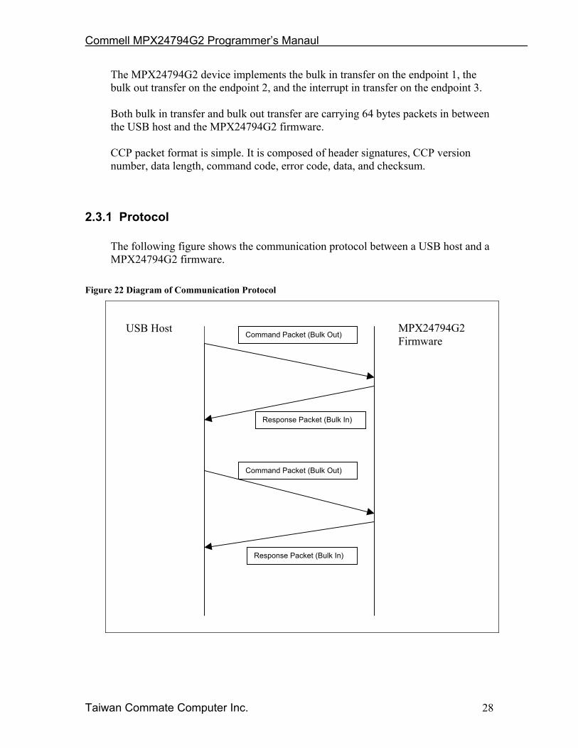
2.3.1 Protocol The following figure shows the communication protocol between a USB host and a MPX24794G2 firmware.
Figure 22 Diagram of Communication Protocol
USB Host MPX24794G2Firmware
Command Packet (Bulk Out)
Response Packet (Bulk In)
Command Packet (Bulk Out)
Response Packet (Bulk In)
Commell MPX24794G2 Programmer’s Manaul
Taiwan Commate Computer Inc. 29
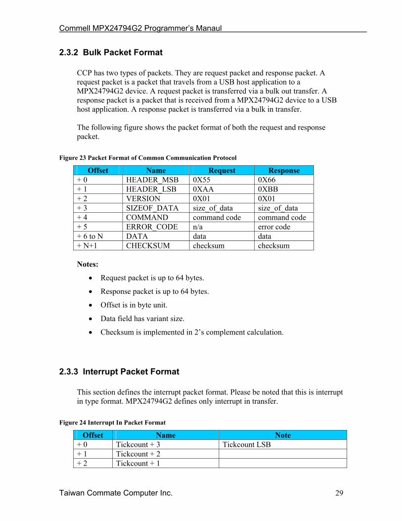
2.3.2 Bulk Packet Format CCP has two types of packets. They are request packet and response packet. A request packet is a packet that travels from a USB host application to a MPX24794G2 device. A request packet is transferred via a bulk out transfer. A response packet is a packet that is received from a MPX24794G2 device to a USB host application. A response packet is transferred via a bulk in transfer. The following figure shows the packet format of both the request and response packet.
Figure 23 Packet Format of Common Communication Protocol
Offset Name Request Response + 0 HEADER_MSB 0X55 0X66 + 1 HEADER_LSB 0XAA 0XBB + 2 VERSION 0X01 0X01 + 3 SIZEOF_DATA size_of_data size_of_data + 4 COMMAND command code command code + 5 ERROR_CODE n/a error code + 6 to N DATA data data + N+1 CHECKSUM checksum checksum Notes:
• Request packet is up to 64 bytes.
• Response packet is up to 64 bytes.
• Offset is in byte unit.
• Data field has variant size.
• Checksum is implemented in 2’s complement calculation.
2.3.3 Interrupt Packet Format This section defines the interrupt packet format. Please be noted that this is interrupt in type format. MPX24794G2 defines only interrupt in transfer.
Figure 24 Interrupt In Packet Format
Offset Name Note + 0 Tickcount + 3 Tickcount LSB + 1 Tickcount + 2 + 2 Tickcount + 1

Commell MPX24794G2 Programmer’s Manaul
Taiwan Commate Computer Inc. 30
+ 3 Tickcount + 0 Tickcount MSB + 4 PRT0DR PRT0DR register value + 5 PRT2DR PRT2DR register value + 6 PRT3DR PRT3DR register value + 7 PRT4DR PRT4DR register value Notes:
• Interrupt in packet is eight bytes long.
• Read this packet via using interrupt in transfer at any time.
• Tick count is a four bytes long unsigned integer.
• PRTxDR fields reflect the PRTxDR register value at the tick count timestamp.
2.3.4 MPX24794G2 Commands This section defines the commands that are used in MPX24794G2 devices. The following command packets are defined.
• CCP_CMND_SYS_GET_SYSTEM_INFO
• CCP_CMND_SYS_GET_TICK_COUNT
• CCP_CMND_SYS_READ_REGISTERS
• CCP_CMND_SYS_WRITE_REGISTERS
• CCP_CMND_GPIO_READ_REGISTERS
• CCP_CMND_GPIO_WRITE_REGISTERS
Commell MPX24794G2 Programmer’s Manaul
Taiwan Commate Computer Inc. 31
2.3.4.1 CCP_CMND_SYS_GET_SYSTEM_INFO PURPOSE: This request / response retrieve the MPX24794G2 system information. FORMAT: Offset Name Request Response
+ 0 HEADER_MSB 0X55 0X66 + 1 HEADER_LSB 0XAA 0XBB + 2 VERSION 0X01 0X01 + 3 SIZEOF_DATA 0X00 0X05 + 4 COMMAND 0X51 0X51 + 5 ERROR_CODE 0X00 error code + 6 DATA_0 checksum 0X04 (number of
bytes return) + 7 DATA_1 0X94 (PID_MSB) + 8 DATA_2 0X05 (PID_LSB) + 9 DATA_3 major_version + 10 DATA_4 minor_version + 11 DATA_5 checksum

Commell MPX24794G2 Programmer’s Manaul
Taiwan Commate Computer Inc. 32
2.3.4.2 CCP_CMND_SYS_GET_TICK_COUNT PURPOSE: This request / response retrieve the MPX24794G2 system tick count. FORMAT: Offset Name Request Response
+ 0 HEADER_MSB 0X55 0X66 + 1 HEADER_LSB 0XAA 0XBB + 2 VERSION 0X01 0X01 + 3 SIZEOF_DATA 0X00 0X05 + 4 COMMAND 0X52 0X51 + 5 ERROR_CODE 0X00 error code + 6 DATA_0 checksum 0X04 (number of
bytes return) + 7 DATA_1 Tickcount + 3 (LSB) + 8 DATA_2 Tickcount + 2 + 9 DATA_3 Tickcount + 1 + 10 DATA_4 Tickcount + 0 (MSB) + 11 DATA_5 checksum

Commell MPX24794G2 Programmer’s Manaul
Taiwan Commate Computer Inc. 33
2.3.4.3 CCP_CMND_SYS_READ_REGISTERS PURPOSE: This request / response reads the CY8C24794 register(s) value. FORMAT: Offset Name Request Response
+ 0 HEADER_MSB 0X55 0X66 + 1 HEADER_LSB 0XAA 0XBB + 2 VERSION 0X01 0X01 + 3 SIZEOF_DATA ?? ?? + 4 COMMAND 0X53 0X53 + 5 ERROR_CODE 0X00 error code + 6 DATA_0 number of
registers to read number of bytes read back
+ 7 DATA_1 reg0_bank byte_0 + 8 DATA_2 reg0_index byte_1 + 9 DATA_3 reserved byte_2 + 10 DATA_4 reg1_bank … + 11 DATA_5 reg1_index checksum + 12 DATA_6 reserved + … … … + … … checksum Notes:
• Up to 20 registers can be read in one packet.
• reg0_bank: The bank number of register0
• reg0_index: The address of register0
Commell MPX24794G2 Programmer’s Manaul
Taiwan Commate Computer Inc. 34
2.3.4.4 CCP_CMND_SYS_WRITE_REGISTERS PURPOSE: This request / response writes the value(s) to the specified CY8C24794 register(s). FORMAT: Offset Name Request Response
+ 0 HEADER_MSB 0X55 0X66 + 1 HEADER_LSB 0XAA 0XBB + 2 VERSION 0X01 0X01 + 3 SIZEOF_DATA ?? 0X01 + 4 COMMAND 0X54 0X54 + 5 ERROR_CODE 0X00 error code + 6 DATA_0 number of
registers to write
number of bytes written
+ 7 DATA_1 reg0_bank checksum + 8 DATA_2 reg0_index + 9 DATA_3 reg0_value + 10 DATA_4 reg1_bank + 11 DATA_5 reg1_index + 12 DATA_6 reg1_value + … … … + … … checksum Notes:
• Up to 20 registers can be read in one packet.
• reg0_bank: The bank number of register0
• reg0_index: The address of register0
• reg0_value: The output value

Commell MPX24794G2 Programmer’s Manaul
Taiwan Commate Computer Inc. 35
2.3.4.5 CCP_CMND_GPIO_READ_REGISTERS PURPOSE: This request / response reads the GPIO register(s) value(s) of the CY8C24794. FORMAT: Offset Name Request Response
+ 0 HEADER_MSB 0X55 0X66 + 1 HEADER_LSB 0XAA 0XBB + 2 VERSION 0X01 0X01 + 3 SIZEOF_DATA ?? ?? + 4 COMMAND 0X60 0X60 + 5 ERROR_CODE 0X00 error code + 6 DATA_0 number of
registers to read number of bytes read back
+ 7 DATA_1 reg0_bank byte_0 + 8 DATA_2 reg0_addr byte_1 + 9 DATA_3 reserved byte_2 + 10 DATA_4 reg0_bank … + 11 DATA_5 reg0_addr checksum + 12 DATA_6 reserved + … … … + … … checksum Notes:
• Up to four registers can be read in one packet.
• reg0_bank: The bank number of reg0 (either 0 or 1).
• reg0_addr: The address of reg0.

Commell MPX24794G2 Programmer’s Manaul
Taiwan Commate Computer Inc. 36
2.3.4.6 CCP_CMND_GPIO_WRITE_REGISTERS PURPOSE: This request / response writes the value(s) to the specified CY8C24794 GPIO register(s). FORMAT: Offset Name Request Response
+ 0 HEADER_MSB 0X55 0X66 + 1 HEADER_LSB 0XAA 0XBB + 2 VERSION 0X01 0X01 + 3 SIZEOF_DATA ?? 0X01 + 4 COMMAND 0X61 0X61 + 5 ERROR_CODE 0X00 error code + 6 DATA_0 number of
registers to write
number of registers written
+ 7 DATA_1 reg0_bank checksum + 8 DATA_2 reg0_index + 9 DATA_3 reg0_value + 10 DATA_4 reg1_bank + 11 DATA_5 reg1_index + 12 DATA_6 reg1_value + … … … + … … checksum Notes:
• Up to four registers can be read in one packet.
• reg0_bank: The bank number of register0
• reg0_index: The address of register0
• reg0_value: The output value

Commell MPX24794G2 Programmer’s Manaul
Taiwan Commate Computer Inc. 37
3 Software Guide This chapter describes the device driver files organization that you direct the Windows Device Driver Wizard while you are installing its corresponding device driver for your targeting Windows operating system.
3.1 Device Drivers Guide
3.1.1 Device Drivers Organization Figure 25 Device Drivers Organization
3.1.2 Windows 2000
Figure 26 Windows 2000 Device Driver

Commell MPX24794G2 Programmer’s Manaul
Taiwan Commate Computer Inc. 38
3.1.3 Windows XP (32-bit) Device Driver
Figure 27 Windows XP 32-bit Device Driver
3.1.4 Windows XP (64-bit) Device Driver
Figure 28 Windows XP 64-bit Device Driver
Commell MPX24794G2 Programmer’s Manaul
Taiwan Commate Computer Inc. 39
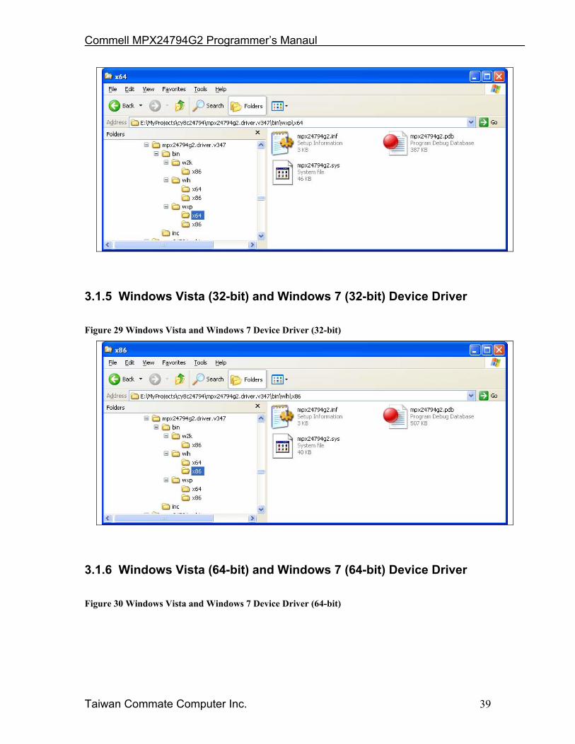
3.1.5 Windows Vista (32-bit) and Windows 7 (32-bit) Device Driver
Figure 29 Windows Vista and Windows 7 Device Driver (32-bit)
3.1.6 Windows Vista (64-bit) and Windows 7 (64-bit) Device Driver
Figure 30 Windows Vista and Windows 7 Device Driver (64-bit)

Commell MPX24794G2 Programmer’s Manaul
Taiwan Commate Computer Inc. 40
3.1.7 GUID This section defines the GUID for MPX24794G2 device. DEFIN_GUID DEFINE_GUID(MPX24794G2_GUID, 0xc9b7b59a, 0xc8ca, 0x431f, 0xa4, 0x73, 0x47, 0xac, 0xa4, 0x63, 0x9c, 0x3a); static const GUID /* MPX24794G2 GUID */ // {C9B7B59A-C8CA-431f-A473-47ACA4639C3A} static GUID MPX24794G2_GUID = {0xc9b7b59a, 0xc8ca, 0x431f, 0xa4, 0x73, 0x47, 0xac, 0xa4, 0x63, 0x9c, 0x3a};
3.2 How to Install Device Driver Please refer to the “MPX-24794G2 User’s Manual”.
3.3 Cypress CyUSB One way to experience and program MPX24794G2 device is through the use Cypress CyUSB tools. CyConsole is one of the tools. Please refer to CyConsole documents for how to use this tool.

Commell MPX24794G2 Programmer’s Manaul
Taiwan Commate Computer Inc. 41
Please refer to CyAPI information for C/C++ programming. Please refer to CyUSB.NET information for .NET programming.
Figure 31 Cypress cyUSB Tools
3.3.1 CyConsole CyConsole can use used to test the Common Communicate Protocol commands defined for MPX-24794G2 device. Please make sure that you have installed the corresponding mpx24794g2.sys onto your target Windows operating system. You then select the installed mpx24794g2.sys device driver when you launch the CyConsole application. A figure shows all endpoints that the MPX24794G2 offers. These include endpoint 1 as the bulk in transfer endpoint, endpoint 2 as the bulk out transfer endpoint, and endpoint 3 as the interrupt in transfer endpoint.

Commell MPX24794G2 Programmer’s Manaul
Taiwan Commate Computer Inc. 42
Figure 32 Select mpx24794g2.sys

Commell MPX24794G2 Programmer’s Manaul
Taiwan Commate Computer Inc. 43
Figure 33 MPX24794G2 Endpoints

Commell MPX24794G2 Programmer’s Manaul
Taiwan Commate Computer Inc. 44
3.3.2 CyAPI Please refer to the documentations in the CyAPI folder. The mpx24794.h file defines the Commell GUID of the Commell MPX-24794G2 USB-GPIO card. Includes this header file into your program file.
3.3.3 CyUSB.NET Please refer to the documentations in the CyUSB.NET folder. We have redistributed the Cypress CyUSB Suite 3.4.7 on the MPX24794G2 CD for your convenience.
3.4 Programming Guide This section describes how your Windows programs interact with the MPX24794G2 firmware via USB transfers. There are three endpoints implemented in the MPX24794G2 device. Bulk-in transfers are implemented on endpoint 1. Bulk-out transfers are implemented on endpoint 2. Interrupt-in transfers are implemented on endpoint 3. MPX24794G2 implements Common Communication Protocol (CCP) version 1 for communication between USB hosts and MPX24794G2 devices. Request packets are sent to the MPX24794G2 firmware via USB bulk out transfers over the endpoint 2, while Response packets are received immediately via USB bulk in transfers over the endpoint 1. Use USB interrupt-in transfers to retrieve MPX24794G2 interrupt packet at any time. MPX24794G2 interrupt packet contains a timestamp, and the register values of PRT0DR, PRT2DR, PRT3DR, and PRT4DR.
3.4.1 MPX-24794G2 Common Communication Protocol Applications communicate with MPX-24794G2 firmware via Common Communication protocol. Request packets are sent via bulk-out transfers while Response packets are received via immediately bulk-in transfers. The following diagram shows how the common communication protocol is operating.
Figure 34 Common Communication Protocol

Commell MPX24794G2 Programmer’s Manaul
Taiwan Commate Computer Inc. 45
Notes:
• Bulk out transfer is used to send request packet out from the host side to the MPX24794G2 firmware side.
• Bulk in transfer is used to receive response packet from the MPX24794G2 firmware side.
• A request packet is 64 bytes. • A response packet is 64 bytes. • The Common Communication Protocol is a paired protocol. That is a
response packet is the result of the last request packet.
3.4.2 Shadow Register Programming You programs need to implement shadow register solution if your application meets the criteria of the read/modify/write effects. Here is an example of how you implement shadow register solution in your C/C++ programs.
USB Host MPX24794G2Firmware
Request Packet (Bulk Out)
Response Packet (Bulk In)
Request Packet (Bulk Out)
Response Packet (Bulk In)
Commell MPX24794G2 Programmer’s Manaul
Taiwan Commate Computer Inc. 46
/* Declare each shadow registers as global variables */ extern unsigned char Port_0_Data_SHADE; extern unsigned char Port_2_Data_SHADE; extern unsigned char Port_3_Data_SHADE; extern unsigned char Port_4_Data_SHADE; Keep these global variables for the output register values for the Port 0, Port 2, Port 3, and Port 4. Initialize these variables as your program wants to initialize PRT0DR, PRT2DR, PRT3DR, and PRT4DR registers. Keep these variables up to synchronous while your program is using the command/response protocol.
3.4.3 C/C++ Programming The CyAPI.lib needs to be linked with your application. Both the “cyapi.h” file and “mpx24794.h” header files need to be included into your project. Your new CCyUSBDevice( ) needs to have “MPX24794G2_GUID” constant specified as the second parameter in order to access Commell MPX-24794G2 USB-GPIO card. Example: #include "cyapi.h" #include "mpx24794.h" void main() { CCyUSBDevice *USBDevice; USB_DEVICE_DESCRIPTOR descr; /* Create an instance of CCyUSBDevice */ USBDevice = new CCyUSBDevice(NULL, MPX24794G2_GUID, true); }
3.4.4 .NET Class Library CyUSB.dll is a managed Microsoft .NET class library. It provides a high-level, powerful programming interface to USB devices. Because CyUSB.dll is a managed .NET library, its classes and methods can be accessed from any of the Microsoft Visual Studio .NET managed languages such as Visual Basic .NET, C#, Visual J#, and managed C++.
Commell MPX24794G2 Programmer’s Manaul
Taiwan Commate Computer Inc. 47
To use the library, you need to add a reference to CyUSB.dll to your project’s Reference folder. Then any source file that access the CyUSB namespace will need to include a line to include the namespace in the appropriate syntax. The library employs a model of DeviceList, Devices and EndPoints. An application will normally create an instance of the USBDeviceList class, which represents a list of USB devices. Each of those devices can then be accessed individually. Please refer to the “Cypress CyUSB .NET DLL Programmer’s Reference” of the Cypress USB Suite v3.4.7 for detail information. We have redistributed this Cypress CyUSB suite 3.4.7 on the MPX24794G2 CD for your convenience.

Commell MPX24794G2 Programmer’s Manaul
Taiwan Commate Computer Inc. 48
4 MPX24794G2 SDK for Windows This chapter describes the MPX24794G2 SDK for Microsoft Windows Environments. Microsoft Visual Studio 2010 is the development tool that this SDK is implemented. MPX24794G2 SDK is provided for the convenient for MPX24794G2 applications programmers. Header files, LIB file, and DLL files need to be includes into your project for rapidly starts.
4.1 File Organization This section defines the files organization of MPX24794G2 SDK. Include these files into your project.
Figure 35 MPX24794G2 SDK files organization
4.2 Files The following files are included into the SDK.
• ccpconst.h – Defines constants used in CCP.

Commell MPX24794G2 Programmer’s Manaul
Taiwan Commate Computer Inc. 49
• ccperrs.h – Define error codes used in CCP.
• mpxguids.h – Defines GUIDs.
• mytypes.h – Defines some types used in the SDK.
• cy24794.h – Defines constants for CY8C24794 controller.
• mpx24794g2.h – Defines API prototypes.
• mpx24794g2x86.lib – API library file for linking.
• mpx24794g2x86.dll – DLL file for API implementations. Copy this file into the working folder of your application or copy this file to the SYSTEM folder, for example, c:\windows\system32.
4.3 Project Example The following figure shows a Microsoft Visual 2010 example for the MPX24794G2 project usedll.
Figure 36 VS2010 example project
Commell MPX24794G2 Programmer’s Manaul
Taiwan Commate Computer Inc. 50
4.4 Sample Codes This example shows how to use MPX24794G2 SDK. // usedll.cpp : Defines the entry point for the console application. // Demonstrate how to implicitly link mpx24794g2.dll. // 1. create a project // 2. add the mpx24794g2.lib into the project // 3. include mpx24794g2.h // 4. include all other head files. // 5. call API specified in mpx24794g2.h // // #include "stdafx.h" #include <Windows.h> #include <Guiddef.h> #include <stdio.h> #include <conio.h> #include "mytypes.h" #include "ccpconst.h" #include "ccperrs.h" #include "mpxguids.h" #include "cy24794.h" #include "mpx24794g2.h" HANDLE hDevice0; HANDLE hDevice1; wchar_t Device0SN[256]; wchar_t Device1SN[256]; /* mode1: strong drive */ unsigned char dmxs[12] = {0XFF,0X00,0X00, 0XFF,0X00,0X00, 0XFF,0X00,0X00, 0XFF,0X00,0X00}; unsigned char drs_ff[4] = {0XFF,0XFF,0XFF,0XFF}; unsigned char drs_00[4] = {0X00,0X00,0X00,0X00}; unsigned char intpkt[8]; unsigned long *ptimestamp; int _tmain(int argc, _TCHAR* argv[]) { int ch; int err; unsigned short ids; unsigned char major, minor; int count; int i; unsigned char pin, dr; hDevice0 = CCP_Open(NULL, MPX24794G2_GUID, 0); if(NULL == hDevice0) { CCP_Close(hDevice0); printf("Failed to open device. Press any key to exit...\n");
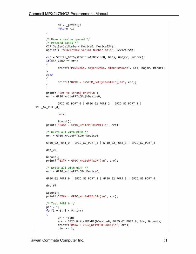
Commell MPX24794G2 Programmer’s Manaul
Taiwan Commate Computer Inc. 51
ch = _getch(); return ‐1; } /* Have a device opened */ /* Proceed tasks */ CCP_GetSerialNumber(hDevice0, Device0SN); wprintf(L"MPX24794G2 Serial Number:%s\n", Device0SN); err = SYSTEM_GetSystemInfo(hDevice0, &ids, &major, &minor); if(ERR_ZERO == err) { printf("PID=0X%X, major=0X%X, minor=0X%X\n", ids, major, minor); } else { printf("0X%X = SYSTEM_GetSystemInfo()\n", err); } printf("Set to strong drive\n"); err = GPIO_WritePRTxDMx(hDevice0, GPIO_G2_PORT_0 | GPIO_G2_PORT_2 | GPIO_G2_PORT_3 | GPIO_G2_PORT_4, dmxs, &count); printf("0X%X = GPIO_WritePRTxDMx()\n", err); /* Write all with 0X00 */ err = GPIO_WritePRTxDR(hDevice0, GPIO_G2_PORT_0 | GPIO_G2_PORT_2 | GPIO_G2_PORT_3 | GPIO_G2_PORT_4, drs_00, &count); printf("0X%X = GPIO_WritePRTxDR()\n", err); /* Write all with 0XFF */ err = GPIO_WritePRTxDR(hDevice0, GPIO_G2_PORT_0 | GPIO_G2_PORT_2 | GPIO_G2_PORT_3 | GPIO_G2_PORT_4, drs_ff, &count); printf("0X%X = GPIO_WritePRTxDR()\n", err); /* Test PORT 0 */ pin = 1; for(i = 0; i < 9; i++) { dr = ~pin; err = GPIO_WritePRTxDR(hDevice0, GPIO_G2_PORT_0, &dr, &count); printf("0X%X = GPIO_WritePRTxDR()\n", err); pin <<= 1;

Commell MPX24794G2 Programmer’s Manaul
Taiwan Commate Computer Inc. 52
} /* Test PORT 2 */ pin = 1; for(i = 0; i < 9; i++) { dr = ~pin; err = GPIO_WritePRTxDR(hDevice0, GPIO_G2_PORT_2, &dr, &count); printf("0X%X = GPIO_WritePRTxDR()\n", err); pin <<= 1; } /* Test PORT 3 */ pin = 1; for(i = 0; i < 9; i++) { dr = ~pin; err = GPIO_WritePRTxDR(hDevice0, GPIO_G2_PORT_3, &dr, &count); printf("0X%X = GPIO_WritePRTxDR()\n", err); pin <<= 1; } /* Test PORT 4 */ pin = 1; for(i = 0; i < 9; i++) { dr = ~pin; err = GPIO_WritePRTxDR(hDevice0, GPIO_G2_PORT_4, &dr, &count); printf("0X%X = GPIO_WritePRTxDR()\n", err); pin <<= 1; } CCP_Close(hDevice0); #if 0 printf("Press any key to exit...\n"); ch = _getch(); #endif return 0; }

Commell MPX24794G2 Programmer’s Manaul
Taiwan Commate Computer Inc. 53
5 API Reference This chapter defines the APIs that are also specified in mpx24794g2.h header file. Use mpx24794g2.h and other relevant header files for your project.

Commell MPX24794G2 Programmer’s Manaul
Taiwan Commate Computer Inc. 54
5.1 CCP_Open /** API: CCP_Open */ extern HANDLE __cdecl CCP_Open(HANDLE hnd, GUID guid, int nDevice); API CCP_Open PURPOSE To open an attaching USB device that has guid tagged in the device
driver. ARGUMENT HANDLE hnd
Application handle to receive USB PnP messages. Set to NULL if not desired.
ARGUMENT GUID guid The target USB device’s GUID
ARGUMENT int nDevice 0‐based device instance number to open.
RETURN NULL if failed to open. NOTES • An attaching MPX24794G2 device cannot be used without a successful
CCP_Open function called. • Store this handle for your later use. • nDevice is equal to value 0 if there is only one MPX24794G2 device
attaching to the system. • nDevice is used to distinguish among multiple MPX24794G2 devices
that are connecting to the same system at the same time. • Use SYSTEM_GetSerialNumber to tell the MPX24794G2 device that your
program wants to program. Example:
Commell MPX24794G2 Programmer’s Manaul
Taiwan Commate Computer Inc. 55
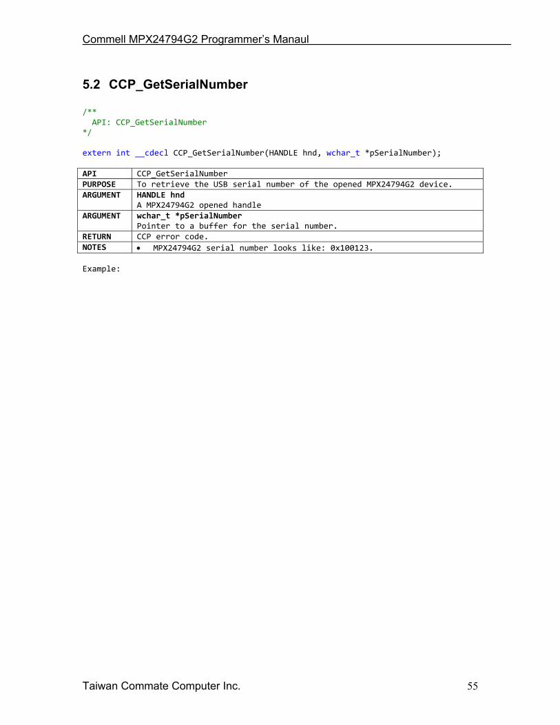
5.2 CCP_GetSerialNumber
/** API: CCP_GetSerialNumber */ extern int __cdecl CCP_GetSerialNumber(HANDLE hnd, wchar_t *pSerialNumber); API CCP_GetSerialNumber PURPOSE To retrieve the USB serial number of the opened MPX24794G2 device. ARGUMENT HANDLE hnd
A MPX24794G2 opened handle ARGUMENT wchar_t *pSerialNumber
Pointer to a buffer for the serial number. RETURN CCP error code. NOTES • MPX24794G2 serial number looks like: 0x100123. Example:
Commell MPX24794G2 Programmer’s Manaul
Taiwan Commate Computer Inc. 56
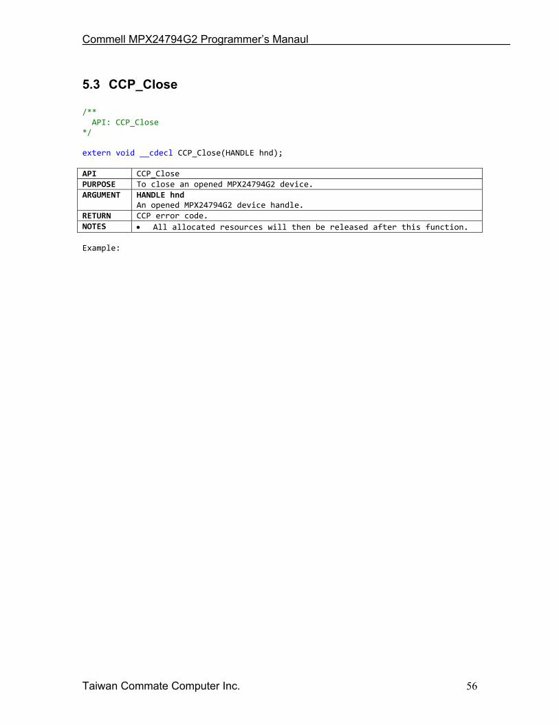
5.3 CCP_Close
/** API: CCP_Close */ extern void __cdecl CCP_Close(HANDLE hnd); API CCP_Close PURPOSE To close an opened MPX24794G2 device. ARGUMENT HANDLE hnd
An opened MPX24794G2 device handle. RETURN CCP error code. NOTES • All allocated resources will then be released after this function. Example:
Commell MPX24794G2 Programmer’s Manaul
Taiwan Commate Computer Inc. 57
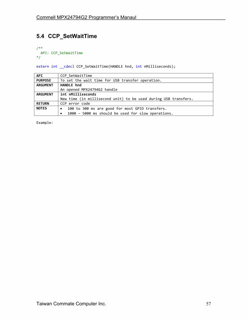
5.4 CCP_SetWaitTime
/** API: CCP_SetWaitTime */ extern int __cdecl CCP_SetWaitTime(HANDLE hnd, int nMilliseconds); API CCP_SetWaitTime PURPOSE To set the wait time for USB transfer operation. ARGUMENT HANDLE hnd
An opened MPX24794G2 handle ARGUMENT int nMilliseconds
New time (in millisecond unit) to be used during USB transfers. RETURN CCP error code NOTES • 100 to 300 ms are good for most GPIO transfers.
• 1000 – 5000 ms should be used for slow operations. Example:
Commell MPX24794G2 Programmer’s Manaul
Taiwan Commate Computer Inc. 58
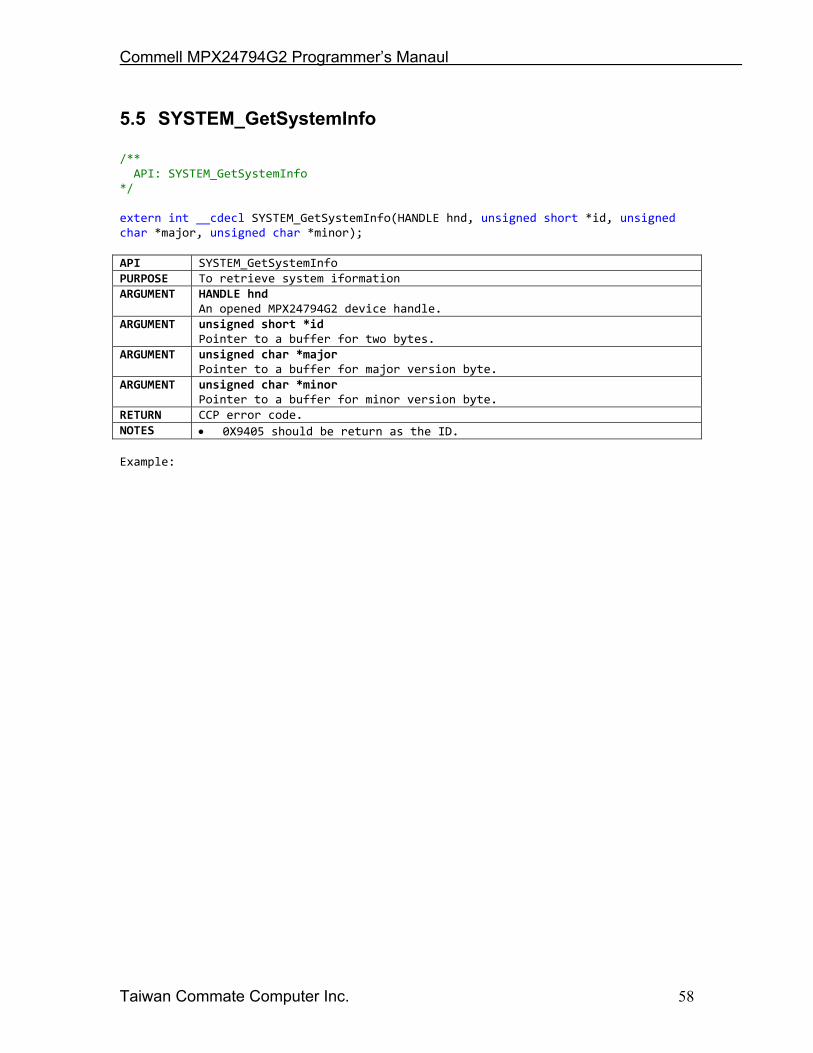
5.5 SYSTEM_GetSystemInfo
/** API: SYSTEM_GetSystemInfo */ extern int __cdecl SYSTEM_GetSystemInfo(HANDLE hnd, unsigned short *id, unsigned char *major, unsigned char *minor); API SYSTEM_GetSystemInfo PURPOSE To retrieve system iformation ARGUMENT HANDLE hnd
An opened MPX24794G2 device handle. ARGUMENT unsigned short *id
Pointer to a buffer for two bytes. ARGUMENT unsigned char *major
Pointer to a buffer for major version byte. ARGUMENT unsigned char *minor
Pointer to a buffer for minor version byte. RETURN CCP error code. NOTES • 0X9405 should be return as the ID. Example:
Commell MPX24794G2 Programmer’s Manaul
Taiwan Commate Computer Inc. 59
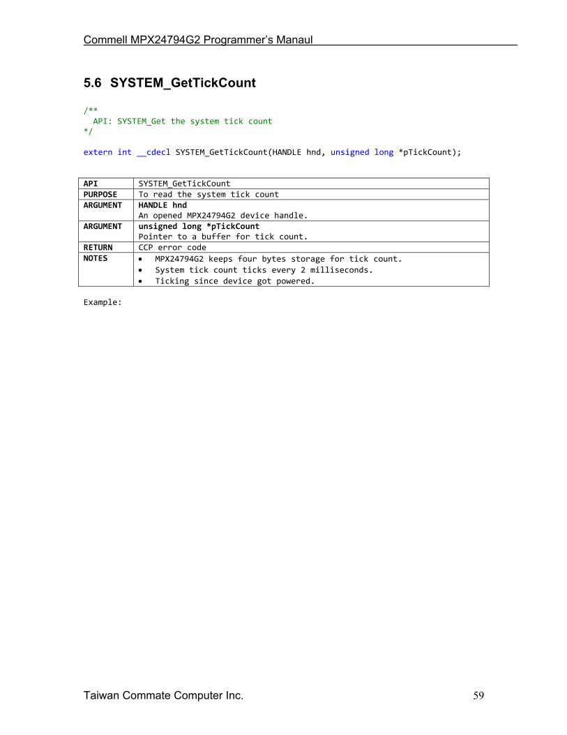
5.6 SYSTEM_GetTickCount
/** API: SYSTEM_Get the system tick count */ extern int __cdecl SYSTEM_GetTickCount(HANDLE hnd, unsigned long *pTickCount); API SYSTEM_GetTickCount PURPOSE To read the system tick count ARGUMENT HANDLE hnd
An opened MPX24794G2 device handle. ARGUMENT unsigned long *pTickCount
Pointer to a buffer for tick count. RETURN CCP error code NOTES • MPX24794G2 keeps four bytes storage for tick count.
• System tick count ticks every 2 milliseconds. • Ticking since device got powered.
Example:
Commell MPX24794G2 Programmer’s Manaul
Taiwan Commate Computer Inc. 60
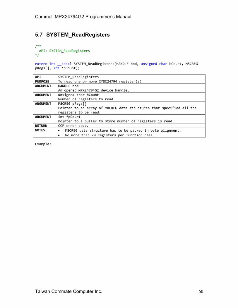
5.7 SYSTEM_ReadRegisters
/** API: SYSTEM_ReadRegisters */ extern int __cdecl SYSTEM_ReadRegisters(HANDLE hnd, unsigned char bCount, M8CREG pRegs[], int *pCount); API SYSTEM_ReadRegisters PURPOSE To read one or more CY8C24794 register(s) ARGUMENT HANDLE hnd
An opened MPX24794G2 device handle. ARGUMENT unsigned char bCount
Number of registers to read. ARGUMENT M8CREG pRegs[]
Pointer to an array of M8CREG data structures that specified all the registers to be read.
ARGUMENT int *pCount Pointer to a buffer to store number of registers is read.
RETURN CCP error code. NOTES • M8CREG data structure has to be packed in byte alignment.
• No more than 20 registers per function call. Example:

Commell MPX24794G2 Programmer’s Manaul
Taiwan Commate Computer Inc. 61
5.8 SYSTEM_WriteRegisters
/** API: SYSTEM_WriteRegisters */ extern int __cdecl SYSTEM_WriteRegisters(HANDLE hnd, unsigned char bCount, M8CREG pRegs[], int *pCount); API SYSTEM_WriteRegisters PURPOSE To write one or more CY8C24794 register(s) ARGUMENT HANDLE hnd
An opened MPX24794G2 device handle. ARGUMENT unsigned char bCount
Number of registers to write to. ARGUMENT M8CREG pRegs[]
Pointer to an array of M8CREG data structures that specified all the registers to be written.
ARGUMENT int *pCount Pointer to a buffer to store number of registers is written.
RETURN CCP error code. NOTES • M8CREG data structure has to be packed in byte alignment.
• No more than 20 registers per function call. Example:
Commell MPX24794G2 Programmer’s Manaul
Taiwan Commate Computer Inc. 62
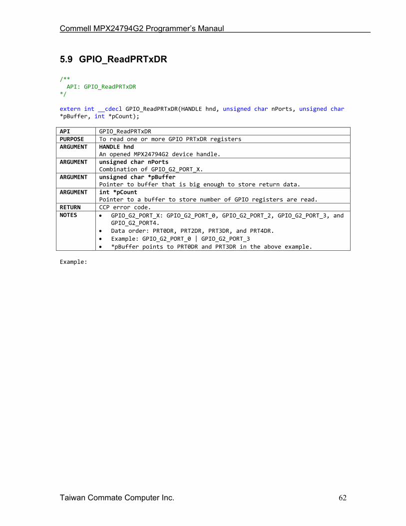
5.9 GPIO_ReadPRTxDR
/** API: GPIO_ReadPRTxDR */ extern int __cdecl GPIO_ReadPRTxDR(HANDLE hnd, unsigned char nPorts, unsigned char *pBuffer, int *pCount); API GPIO_ReadPRTxDR PURPOSE To read one or more GPIO PRTxDR registers ARGUMENT HANDLE hnd
An opened MPX24794G2 device handle. ARGUMENT unsigned char nPorts
Combination of GPIO_G2_PORT_X. ARGUMENT unsigned char *pBuffer
Pointer to buffer that is big enough to store return data. ARGUMENT int *pCount
Pointer to a buffer to store number of GPIO registers are read. RETURN CCP error code. NOTES • GPIO_G2_PORT_X: GPIO_G2_PORT_0, GPIO_G2_PORT_2, GPIO_G2_PORT_3, and
GPIO_G2_PORT4. • Data order: PRT0DR, PRT2DR, PRT3DR, and PRT4DR. • Example: GPIO_G2_PORT_0 | GPIO_G2_PORT_3 • *pBuffer points to PRT0DR and PRT3DR in the above example.
Example:

Commell MPX24794G2 Programmer’s Manaul
Taiwan Commate Computer Inc. 63
5.10 GPIO_WritePRTxDR
/** API: GPIO_WritePRTxDR */ extern int __cdecl GPIO_WritePRTxDR(HANDLE hnd, unsigned char nPorts, unsigned char *pBuffer, int *pCount); API GPIO_WritePRTxDR PURPOSE To write one or more GPIO PRTxDR registers ARGUMENT HANDLE hnd
An opened MPX24794G2 device handle. ARGUMENT unsigned char nPorts
Combination of GPIO_G2_PORT_X. ARGUMENT unsigned char *pBuffer
Pointer to buffer for output data. ARGUMENT int *pCount
Pointer to a buffer to store the number of GPIO registers are written. RETURN CCP error code. NOTES • GPIO_G2_PORT_X: GPIO_G2_PORT_0, GPIO_G2_PORT_2, GPIO_G2_PORT_3, and
GPIO_G2_PORT4. • Data order: PRT0DR, PRT2DR, PRT3DR, and PRT4DR. • Example: GPIO_G2_PORT_0 | GPIO_G2_PORT_3 • pBuffer points to PRT0DR and PRT3DR in the above example.
Example:
Commell MPX24794G2 Programmer’s Manaul
Taiwan Commate Computer Inc. 64
5.11 GPIO_ReadPRTxIE
/** API: GPIO_ReadPRTxIE */ extern int __cdecl GPIO_ReadPRTxIE(HANDLE hnd, unsigned char nPorts, unsigned char *pBuffer, int *pCount); API GPIO_ReadPRTxIE PURPOSE To read one or more GPIO PRTxIE registers ARGUMENT HANDLE hnd
An opened MPX24794G2 device handle. ARGUMENT unsigned char nPorts
Combination of GPIO_G2_PORT_X. ARGUMENT unsigned char *pBuffer
Pointer to buffer that is big enough to store return data. ARGUMENT int *pCount
Pointer to a buffer to store number of GPIO registers are read. RETURN CCP error code. NOTES • GPIO_G2_PORT_X: GPIO_G2_PORT_0, GPIO_G2_PORT_2, GPIO_G2_PORT_3, and
GPIO_G2_PORT4. • Data order: PRT0IE, PRT2IE, PRT3IE, and PRT4IE. • Example: GPIO_G2_PORT_0 | GPIO_G2_PORT_3 • The return data format is arranged in ascending port number. For
example, *(pBuffer + 0) is PRT0IE, *(pBuffer + 1) is PRT3IE in the above Example.
Example:
Commell MPX24794G2 Programmer’s Manaul
Taiwan Commate Computer Inc. 65
5.12 GPIO_WritePRTxIE
/** API: GPIO_WritePRTxIE */ extern int __cdecl GPIO_WritePRTxIE(HANDLE hnd, unsigned char nPorts, unsigned char *pBuffer, int *pCount); API GPIO_WritePRTxIE PURPOSE To write one or more GPIO PRTxIE registers ARGUMENT HANDLE hnd
An opened MPX24794G2 device handle. ARGUMENT unsigned char nPorts
Combination of GPIO_G2_PORT_X. ARGUMENT unsigned char *pBuffer
Pointer to buffer for output data. ARGUMENT int *pCount
Pointer to a buffer to store number of GPIO registers are written. RETURN CCP error code. NOTES • GPIO_G2_PORT_X: GPIO_G2_PORT_0, GPIO_G2_PORT_2, GPIO_G2_PORT_3, and
GPIO_G2_PORT4. • Data order: PRT0IE, PRT2IE, PRT3IE, and PRT4IE. • Example: GPIO_G2_PORT_0 | GPIO_G2_PORT_3 • pBuffer points to PRT0IE and PRT3IE.
Example:

Commell MPX24794G2 Programmer’s Manaul
Taiwan Commate Computer Inc. 66
5.13 GPIO_ReadPRTxICx
/** API: GPIO_ReadPRTxICx */ extern int __cdecl GPIO_ReadPRTxICx(HANDLE hnd, unsigned char nPorts, unsigned char *pBuffer, int *pCount); API GPIO_ReadPRTxICx PURPOSE To read one or more GPIO PRTxICx registers ARGUMENT HANDLE hnd
An opened MPX24794G2 device handle. ARGUMENT unsigned char nPorts
Combination of GPIO_G2_PORT_X. ARGUMENT unsigned char *pBuffer
Pointer to buffer that is big enough to store return data. ARGUMENT int *pCount
Pointer to a buffer to store the number of GPIO registers are read. RETURN CCP error code. NOTES • GPIO_G2_PORT_X: GPIO_G2_PORT_0, GPIO_G2_PORT_2, GPIO_G2_PORT_3, and
GPIO_G2_PORT4. • Data order: PRT0IC0, PRT0IC1, PRT2IC0, PRT2IC1, PRT3IC0, PRT3IC1,
PRT4IC0,PRT4IC1. • Example: GPIO_G2_PORT_0 | GPIO_G2_PORT_3 • The return data format is arranged in ascending port number. For
example, *(pBuffer + 0) is PRT0IC0, *(pBuffer + 1) is PRT0IC1, *(pBuffer + 2) is PRT3IC0, and *(pBuffer + 3) is PRT3IC1 in the above Example.
Example:

Commell MPX24794G2 Programmer’s Manaul
Taiwan Commate Computer Inc. 67
5.14 GPIO_WritePRTxICx
/** API: GPIO_WritePRTxICx */ extern int __cdecl GPIO_WritePRTxICx(HANDLE hnd, unsigned char nPorts, unsigned char *pBuffer, int *pCount); API GPIO_WritePRTxICx PURPOSE To write one or more GPIO PRTxICx registers ARGUMENT HANDLE hnd
An opened MPX24794G2 device handle. ARGUMENT unsigned char nPorts
Combination of GPIO_G2_PORT_X. ARGUMENT unsigned char *pBuffer
Pointer to buffer for output data. ARGUMENT int *pCount
Pointer to a buffer to store number of GPIO registers are written. RETURN CCP error code. NOTES • GPIO_G2_PORT_X: GPIO_G2_PORT_0, GPIO_G2_PORT_2, GPIO_G2_PORT_3, and
GPIO_G2_PORT4. • Data order: PRT0IC0, PRT0IC1, PRT2IC0, PRT2IC1, PRT3IC0, PRT3IC1,
PRT4IC0, and PRT4IC1. • Example: GPIO_G2_PORT_0 | GPIO_G2_PORT_3 • *(pBuffer + 0) is PRT0IC0, *(pBuffer + 1) is PRT0IC1, *(pBuffer +
2) is PRT3IC0, and *(pBuffer + 3) is PRT3IC1 in the above Example. Example:
Commell MPX24794G2 Programmer’s Manaul
Taiwan Commate Computer Inc. 68
5.15 GPIO_ReadPRTxDMx
/** API: GPIO_ReadPRTxDMx */ extern int __cdecl GPIO_ReadPRTxDMx(HANDLE hnd, unsigned char nPorts, unsigned char *pBuffer, int *pCount); API GPIO_ReadPRTxDMx PURPOSE To read one or more GPIO PRTxDMx registers ARGUMENT HANDLE hnd
An opened MPX24794G2 device handle. ARGUMENT unsigned char nPorts
Combination of GPIO_G2_PORT_X. ARGUMENT unsigned char *pBuffer
Pointer to buffer that is big enough to store return data. ARGUMENT int *pCount
Pointer to a buffer to store number of GPIO registers are read. RETURN CCP error code. NOTES • GPIO_G2_PORT_X: GPIO_G2_PORT_0, GPIO_G2_PORT_2, GPIO_G2_PORT_3, and
GPIO_G2_PORT4. • Data order: PRT0DM0, PRT0DM1, PRT0DM2, PRT2DM0, PRT2DM1, PRT2DM2,
PRT3DM0, PRT3DM1, PRT3DM2, PRT4DM0, PRT4DM1, and PRT4DM2. • Example: GPIO_G2_PORT_0 | GPIO_G2_PORT_3 • *pBuffer points to PRT0DM0, PRT0DM1, PRT0DM2, PRT3DM0, PRT3DM1, and
PRT3DM2 in the above example. Example:
Commell MPX24794G2 Programmer’s Manaul
Taiwan Commate Computer Inc. 69
5.16 GPIO_WritePRTxDMx
/** API: GPIO_WritePRTxDMx */ extern int __cdecl GPIO_WritePRTxDMx(HANDLE hnd, unsigned char nPorts, unsigned char *pBuffer, int *pCount); API GPIO_WritePRTxDMx PURPOSE To write one or more GPIO PRTxDMx registers ARGUMENT HANDLE hnd
An opened MPX24794G2 device handle. ARGUMENT unsigned char nPorts
Combination of GPIO_G2_PORT_X. ARGUMENT unsigned char *pBuffer
Pointer to buffer for output data. ARGUMENT int *pCount
Pointer to a buffer to store the number of GPIO registers are written. RETURN CCP error code. NOTES • GPIO_G2_PORT_X: GPIO_G2_PORT_0, GPIO_G2_PORT_2, GPIO_G2_PORT_3, and
GPIO_G2_PORT4. • Data order: PRT0DM0, PRT0DM1, PRT0DM2, PRT3DM0, PRT3DM1, PRT3DM2,
PRT4DM0, PRT4DM1, and PRT4DM2. • Example: GPIO_G2_PORT_0 | GPIO_G2_PORT_3 • *pBuffer points to PRT0DM0, PRT0DM1, PRT0DM2, PRT3DM0, PRT3DM1, and
PRT3DM2. Example:

Commell MPX24794G2 Programmer’s Manaul
Taiwan Commate Computer Inc. 70
5.17 GPIO_SetModePort
/** API: GPIO_SetModePort */ extern int __cdecl GPIO_SetModePort(HANDLE hnd, unsigned char nPort, unsigned char nMode); API GPIO_SetModePort PURPOSE To set a GPIO port into one of the eight modes ARGUMENT HANDLE hnd
An opened MPX24794G2 device handle. ARGUMENT unsigned char nPorts
One of the GPIO ports. ARGUMENT unsigned char nMode
One of the eight GPIO modes. RETURN CCP error code. NOTES • GPIO ports: GPIO_G2_PORT_0, GPIO_G2_PORT_2, GPIO_G2_PORT_3, and
GPIO_G2_PORT4. • Eight modes: GPIO_MODE_0, GPIO_MODE_1, GPIO_MODE_2, GPIO_MODE_3,
GPIO_MODE_4, GPIO_MODE_5, GPIO_MODE_6, and GPIO_MODE_7. • Please refer to cy24794.h file.
Example:
Commell MPX24794G2 Programmer’s Manaul
Taiwan Commate Computer Inc. 71
5.18 GPIO_SetModePin
/** API: GPIO_SetModePin */ extern int __cdecl GPIO_SetModePin(HANDLE hnd, unsigned char nPort, unsigned char nPins, unsigned char nMode); API GPIO_SetModePin PURPOSE To set one or more pins in a GPIO port to one of the eight GPIO modes. ARGUMENT HANDLE hnd
An opened MPX24794G2 device handle. ARGUMENT unsigned char nPorts
One of the GPIO_G2_PORT_x. ARGUMENT unsigned char nPins
Combination of GPIO_PIN_x. ARGUMENT unsigned char nMode
One of the eight GPIO modes. RETURN CCP error code. NOTES • GPIO_G2_PORTx: GPIO_G2_PORT_0, GPIO_G2_PORT_2, GPIO_G2_PORT_3, and
GPIO_G2_PORT4. • GPIO_PIN_x: GPIO_PIN_0, GPIO_PIN_1, GPIO_PIN_2, GPIO_PIN_3,
GPIO_PIN_4, GPIO_PIN_5, GPIO_PIN_6, and GPIO_PIN_7. • GPIO_MODE_x: GPIO_MODE_0, GPIO_MODE_1, GPIO_MODE_2, GPIO_MODE_3,
GPIO_MODE_4, GPIO_MODE_5, GPIO_MODE_6, and GPIO_MODE_7. Example:
Commell MPX24794G2 Programmer’s Manaul
Taiwan Commate Computer Inc. 72
5.19 GPIO_ReadPort
/** API: GPIO_ReadPort */ extern int __cdecl GPIO_ReadPort(HANDLE hnd, unsigned char nPort, unsigned char *pValue); API GPIO_ReadPort PURPOSE To read the specified PRTxDR register. ARGUMENT HANDLE hnd
An opened MPX24794G2 device handle. ARGUMENT unsigned char nPorts
One of the GPIO_G2_PORT_X. ARGUMENT unsigned char *pValue
Pointer to a byte to store the return byte. RETURN CCP error code. NOTES • GPIO_G2_PORT_X: GPIO_G2_PORT_0, GPIO_G2_PORT_2, GPIO_G2_PORT_3, and
GPIO_G2_PORT4. Example:
Commell MPX24794G2 Programmer’s Manaul
Taiwan Commate Computer Inc. 73
5.20 GPIO_WritePort
/** API: GPIO_WritePort Write the specified GPIO port with the specified value \param hnd MPX24794G2 handle \param nPort One of GPIO_G2_PORT_0/2/3/4 \param pValue Pointer to the output value \return CCP error code */ extern int __cdecl GPIO_WritePort(HANDLE hdn, unsigned char nPort, unsigned char bValue); API GPIO_WritePort PURPOSE To write the specified byte to the specified GPIO port. ARGUMENT HANDLE hnd
An opened MPX24794G2 device handle. ARGUMENT unsigned char nPorts
One of the GPIO_G2_PORT_X. ARGUMENT unsigned char bValue
Output value to write to. RETURN CCP error code. NOTES • GPIO_G2_PORT_X: GPIO_G2_PORT_0, GPIO_G2_PORT_2, GPIO_G2_PORT_3, and
GPIO_G2_PORT4. Example:

Commell MPX24794G2 Programmer’s Manaul
Taiwan Commate Computer Inc. 74
5.21 INT_ReadPacket
/** API: INT_ReadPacket */ extern int __cdecl INT_ReadPacket(HANDLE hnd, int nSize, unsigned char *pBuffer); API INT_ReadPacket PURPOSE To read a interrupt‐in packet. ARGUMENT HANDLE hnd
An opened MPX24794G2 device handle. ARGUMENT unsigned char nSize
The size in byte pointed to by pBuffer. ARGUMENT unsigned char *pBuffer
Pointer to a buffer to store the interrupt‐in packet. RETURN CCP error code. NOTES • This function can be called at any time.
• Your program must provide at least 8 bytes long buffer for an interrupt‐in packet.
• The first four bytes store timestamp. • The next four bytes are PRTxDR registers. • Please refer to the Interrupt‐In Packet section for details.
Example:
Commell MPX24794G2 Programmer’s Manaul
Taiwan Commate Computer Inc. 75
6 References [1] CY8C24x94 PSoC Programmable System-on-Chip Technical Reference Manual (TRM). Document No. 001-14463 Rev. *F. [2] Cypress CyAPI Programmer’s Reference, Cypress Suite USB 3.4.2. [3] Cypress CyUSB .NET DLL Programmer’s Reference, Cypress Suite USB 3.4.2. [4] PCI Express Mini Card Electromechanical Specification Revision 1.2, October 26, 2007.