communications chemie - michigan state university ruska centre for microscopy and spectroscopy with...
TRANSCRIPT
German Edition: DOI: 10.1002/ange.201611740PhosphorusInternational Edition: DOI: 10.1002/anie.201611740
Assembly of Ring-Shaped Phosphorus within Carbon NanotubeNanoreactorsJinying Zhang,* Dan Zhao, Dingbin Xiao, Chuansheng Ma, Hongchu Du, Xin Li, Lihui Zhang,Jialiang Huang, Hongyang Huang, Chun-Lin Jia,* David Tom#nek,* and Chunming Niu
Abstract: A phosphorus allotrope that has not been observedso far, ring-shaped phosphorus consisting of alternate P8 andP2 structural units, has been assembled inside multi-walledcarbon nanotube nanoreactors with inner diameters of 5–8 nmby a chemical vapor transport and reaction of red phosphorusat 500 88C. The ring-shaped nanostructures with surroundinggraphene walls are stable under ambient conditions. Thenanostructures were characterized by high-resolution trans-mission electron microscopy, scanning transmission electronmicroscopy, energy-dispersive X-ray spectroscopy, Ramanscattering, attenuated total reflectance Fourier transform infra-red spectroscopy, and X-ray photoelectron spectroscopy.
Two-dimensional (2D) black phosphorus, phosphorene, hasattracted lots of attention owing to its intrinsic electronicproperties.[1–4] However, phosphorene has been found todegrade under ambient conditions[5] and needs to be pro-tected by an inert atmosphere[3] or specific molecules[6, 7]
owing to its reactivity caused by lone electron pairs. Severalother interesting phosphorus allotropes have also beentheoretically predicted.[8–11] Experimentally well-establishedis the white phosphorus allotrope, a molecular solid consistingof P4 molecules. Other established allotropes that have beenproduced experimentally, include Hittorf phosphorus (violetphosphorus),[12] fibrous phosphorus,[13] blue phosphorus,[14]
and black phosphorus,[3,15, 16] as well as amorphous redphosphorus[17] (RP). Published theoretical predictions includea stable ring-shaped phosphorus (r-P) allotrope consisting of
alternating P8 and P2 structural units with minimum stabilityreached for P80,
[10] and coil structures.[11] Carbon nanotubesare effective as nanoreactors to synthesize and containnanostructures.[18–27] Carbon nanotubes also serve as narrowand stable one-dimensional cages that protect the enclosedproducts from degradation under ambient conditions.
Herein, we report experimental evidence for the forma-tion of r-P nanostructures, self-assembled inside a multi-walled carbon nanotube (MWCNT). The r-P nanostructuresinside MWCNTs (r-P@MWCNTs) are stable under ambientconditions. The nanostructures have been characterized byhigh-resolution transmission electron microscopy (HRTEM),scanning transmission electron microscopy (STEM), STEMenergy-dispersive X-ray spectroscopy (EDS), Raman scatter-ing, attenuated total reflectance Fourier transform infraredspectroscopy (ATR-FTIR), and X-ray photoelectron spec-troscopy (XPS).
MWCNTs functioning as nanoreactors were prepared bya CVD method to have less than 0.9% catalyst[28] and purifiedaccording to a reported method.[29] The r-P@MWCNTs wereprepared by a vapor-phase transportation and reactionmethod[19–21,30, 31] at 500 88C using RP as precursor. At 500 88C,RP was sublimed and likely decomposed into differentphosphorus clusters (PCs), which subsequently diffused intoevacuated inner space of MWCNTs and self-assembled toform r-P nanostructures to give an encapsulation yield around60%.
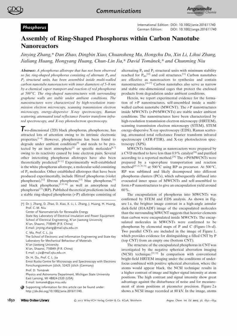
The encapsulation of phosphorus into MWCNTs wasconfirmed by STEM and EDS analysis. As shown in Fig-ure 1a, the brighter image contrast in a high-angle annulardark-field (HAADF) image of the encapsulated moleculesthan the surrounding MWCNT suggests that heavier elementsthan carbon were encapsulated inside MWCNTs. The encap-sulated molecules in MWCNTs were confirmed to bephosphorus by elemental maps of P and C (Figure 1b–d).Two parallel CNTs are included in the image of Figure 1,which provides evidence for distinguishing a filled CNT by P(top CNT) from an empty one (bottom CNT).
The structure of the encapsulated phosphorus in CNT wasinvestigated by the negative spherical aberration imaging(NCSI) technique.[32,33] In comparison with conventionalbright-field HRTEM imaging under the conditions of under-focus combined with positive spherical aberration, where theatoms would appear black, the NCSI technique results ina higher contrast of image and higher signal intensity at atompositions. The high contrast and signal intensity show greatadvantage against the disturbance of noise and for measure-ment of atom positions at picometer precision. Figure 2ashows a NCSI image recorded at 80 kV. In the image, atoms
[*] Dr. J. Zhang, D. Zhao, D. Xiao, X. Li, L. Zhang, J. Huang, H. Huang,Prof. C.-M. NiuCenter of Nanomaterials for Renewable EnergyState Key Laboratory of Electrical Insulation and Power EquipmentSchool of Electrical Engineering, Xi’an Jiaotong UniversityXi’an, Shaanxi, 710049 (P.R. China)E-mail: [email protected]
C. Ma, Prof. C. L. JiaThe School of Electronic and Information Engineering and State KeyLaboratory for Mechanical Behaviour of MaterialsXi’an Jiaotong UniversityXi’an, Shaanxi, 710049 (P.R. China)E-mail: [email protected]
Dr. H. Du, Prof. C. L. JiaErnst Ruska Centre for Microscopy and Spectroscopy with ElectronsForschungszentrum Jflich, 52425 Jflich (Germany)
Prof. D. Tom#nekPhysics and Astronomy Department, Michigan State UniversityEast Lansing, MI 48824-2320 (USA)E-mail: [email protected]
Supporting information for this article can be found under:http://dx.doi.org/10.1002/anie.201611740.
AngewandteChemieCommunications
1850 T 2017 Wiley-VCH Verlag GmbH & Co. KGaA, Weinheim Angew. Chem. Int. Ed. 2017, 56, 1850 –1854
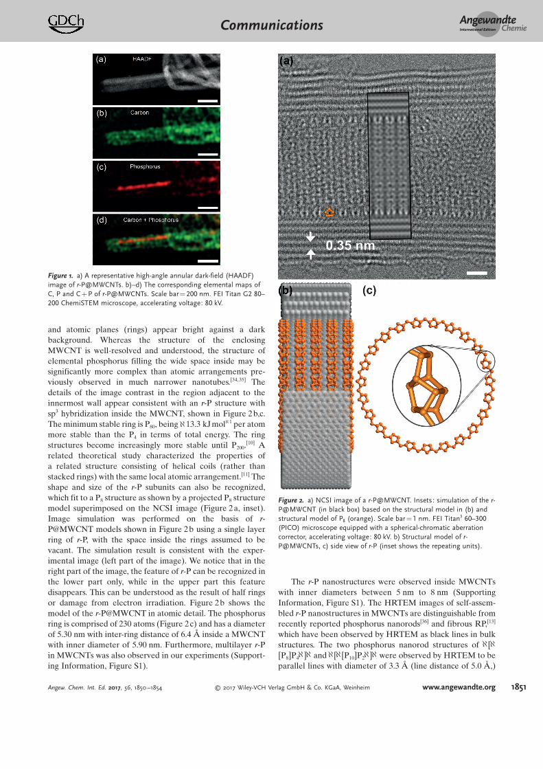
and atomic planes (rings) appear bright against a darkbackground. Whereas the structure of the enclosingMWCNT is well-resolved and understood, the structure ofelemental phosphorus filling the wide space inside may besignificantly more complex than atomic arrangements pre-viously observed in much narrower nanotubes.[34,35] Thedetails of the image contrast in the region adjacent to theinnermost wall appear consistent with an r-P structure withsp3 hybridization inside the MWCNT, shown in Figure 2b,c.The minimum stable ring is P80, [email protected] kJmol@1 per atommore stable than the P4 in terms of total energy. The ringstructures become increasingly more stable until P200.
[10] Arelated theoretical study characterized the properties ofa related structure consisting of helical coils (rather thanstacked rings) with the same local atomic arrangement.[11] Theshape and size of the r-P subunits can also be recognized,which fit to a P8 structure as shown by a projected P8 structuremodel superimposed on the NCSI image (Figure 2a, inset).Image simulation was performed on the basis of r-P@MWCNT models shown in Figure 2b using a single layerring of r-P, with the space inside the rings assumed to bevacant. The simulation result is consistent with the exper-imental image (left part of the image). We notice that in theright part of the image, the feature of r-P can be recognized inthe lower part only, while in the upper part this featuredisappears. This can be understood as the result of half ringsor damage from electron irradiation. Figure 2b shows themodel of the r-P@MWCNT in atomic detail. The phosphorusring is comprised of 230 atoms (Figure 2c) and has a diameterof 5.30 nm with inter-ring distance of 6.4 c inside a MWCNTwith inner diameter of 5.90 nm. Furthermore, multilayer r-Pin MWCNTs was also observed in our experiments (Support-ing Information, Figure S1).
The r-P nanostructures were observed inside MWCNTswith inner diameters between 5 nm to 8 nm (SupportingInformation, Figure S1). The HRTEM images of self-assem-bled r-P nanostructures in MWCNTs are distinguishable fromrecently reported phosphorus nanorods[36] and fibrous RP,[13]
which have been observed by HRTEM as black lines in bulkstructures. The two phosphorus nanorod structures of @[@[P8]P4@]@ and@[@[P10]P2@]@were observed by HRTEM to beparallel lines with diameter of 3.3 c (line distance of 5.0 c,)
Figure 1. a) A representative high-angle annular dark-field (HAADF)image of r-P@MWCNTs. b)–d) The corresponding elemental maps ofC, P and C +P of r-P@MWCNTs. Scale bar = 200 nm. FEI Titan G2 80–200 ChemiSTEM microscope, accelerating voltage: 80 kV.
Figure 2. a) NCSI image of a r-P@MWCNT. Insets: simulation of the r-P@MWCNT (in black box) based on the structural model in (b) andstructural model of P8 (orange). Scale bar =1 nm. FEI Titan3 60–300(PICO) microscope equipped with a spherical-chromatic aberrationcorrector, accelerating voltage: 80 kV. b) Structural model of r-P@MWCNTs, c) side view of r-P (inset shows the repeating units).
AngewandteChemieCommunications
1851Angew. Chem. Int. Ed. 2017, 56, 1850 –1854 T 2017 Wiley-VCH Verlag GmbH & Co. KGaA, Weinheim www.angewandte.org
and 4.7 c (line distance of 5.4 c).[36] On the other hand,parallel strands with distance of 3.2 c were observed fromfibrous RP.[13]
The self-assembled r-P nanostructures inside MWCNTsare stable in air, since the lone pair electrons of phosphorusare passivated by the intact walls of carbon nanotubes(Supporting Information, Figure S1). The ends of self-assem-bled r-P nanostructures at the opening of MWCNTs arepassivated by either an atomically thin layer of amorphouscarbon, or by phosphorus or phosphorus oxides (SupportingInformation, Figure S2). The space restriction imposed byMWCNTs limits volume expansion needed for furtheroxidation and oxygen diffusion when exposed to air. TheHRTEM investigations further confirmed that carbon nano-tubes are efficient Faraday tubes for phosphorus nanostruc-tures.
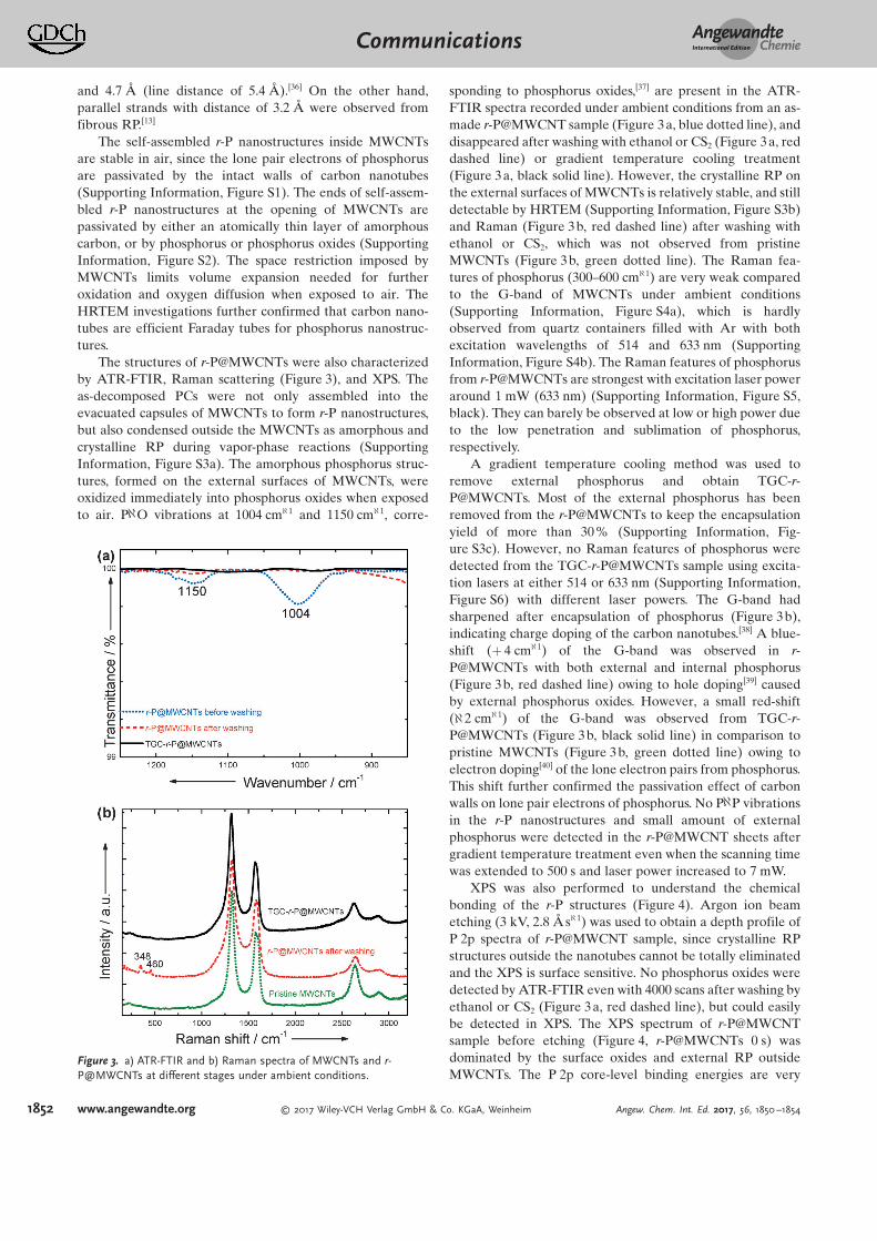
The structures of r-P@MWCNTs were also characterizedby ATR-FTIR, Raman scattering (Figure 3), and XPS. Theas-decomposed PCs were not only assembled into theevacuated capsules of MWCNTs to form r-P nanostructures,but also condensed outside the MWCNTs as amorphous andcrystalline RP during vapor-phase reactions (SupportingInformation, Figure S3a). The amorphous phosphorus struc-tures, formed on the external surfaces of MWCNTs, wereoxidized immediately into phosphorus oxides when exposedto air. P@O vibrations at 1004 cm@1 and 1150 cm@1, corre-
sponding to phosphorus oxides,[37] are present in the ATR-FTIR spectra recorded under ambient conditions from an as-made r-P@MWCNT sample (Figure 3a, blue dotted line), anddisappeared after washing with ethanol or CS2 (Figure 3a, reddashed line) or gradient temperature cooling treatment(Figure 3a, black solid line). However, the crystalline RP onthe external surfaces of MWCNTs is relatively stable, and stilldetectable by HRTEM (Supporting Information, Figure S3b)and Raman (Figure 3b, red dashed line) after washing withethanol or CS2, which was not observed from pristineMWCNTs (Figure 3b, green dotted line). The Raman fea-tures of phosphorus (300–600 cm@1) are very weak comparedto the G-band of MWCNTs under ambient conditions(Supporting Information, Figure S4a), which is hardlyobserved from quartz containers filled with Ar with bothexcitation wavelengths of 514 and 633 nm (SupportingInformation, Figure S4b). The Raman features of phosphorusfrom r-P@MWCNTs are strongest with excitation laser poweraround 1 mW (633 nm) (Supporting Information, Figure S5,black). They can barely be observed at low or high power dueto the low penetration and sublimation of phosphorus,respectively.
A gradient temperature cooling method was used toremove external phosphorus and obtain TGC-r-P@MWCNTs. Most of the external phosphorus has beenremoved from the r-P@MWCNTs to keep the encapsulationyield of more than 30% (Supporting Information, Fig-ure S3c). However, no Raman features of phosphorus weredetected from the TGC-r-P@MWCNTs sample using excita-tion lasers at either 514 or 633 nm (Supporting Information,Figure S6) with different laser powers. The G-band hadsharpened after encapsulation of phosphorus (Figure 3b),indicating charge doping of the carbon nanotubes.[38] A blue-shift (+ 4 cm@1) of the G-band was observed in r-P@MWCNTs with both external and internal phosphorus(Figure 3b, red dashed line) owing to hole doping[39] causedby external phosphorus oxides. However, a small red-shift(@2 cm@1) of the G-band was observed from TGC-r-P@MWCNTs (Figure 3b, black solid line) in comparison topristine MWCNTs (Figure 3 b, green dotted line) owing toelectron doping[40] of the lone electron pairs from phosphorus.This shift further confirmed the passivation effect of carbonwalls on lone pair electrons of phosphorus. No P@P vibrationsin the r-P nanostructures and small amount of externalphosphorus were detected in the r-P@MWCNT sheets aftergradient temperature treatment even when the scanning timewas extended to 500 s and laser power increased to 7 mW.
XPS was also performed to understand the chemicalbonding of the r-P structures (Figure 4). Argon ion beametching (3 kV, 2.8 c s@1) was used to obtain a depth profile ofP 2p spectra of r-P@MWCNT sample, since crystalline RPstructures outside the nanotubes cannot be totally eliminatedand the XPS is surface sensitive. No phosphorus oxides weredetected by ATR-FTIR even with 4000 scans after washing byethanol or CS2 (Figure 3a, red dashed line), but could easilybe detected in XPS. The XPS spectrum of r-P@MWCNTsample before etching (Figure 4, r-P@MWCNTs 0 s) wasdominated by the surface oxides and external RP outsideMWCNTs. The P 2p core-level binding energies are very
Figure 3. a) ATR-FTIR and b) Raman spectra of MWCNTs and r-P@MWCNTs at different stages under ambient conditions.
AngewandteChemieCommunications
1852 www.angewandte.org T 2017 Wiley-VCH Verlag GmbH & Co. KGaA, Weinheim Angew. Chem. Int. Ed. 2017, 56, 1850 –1854
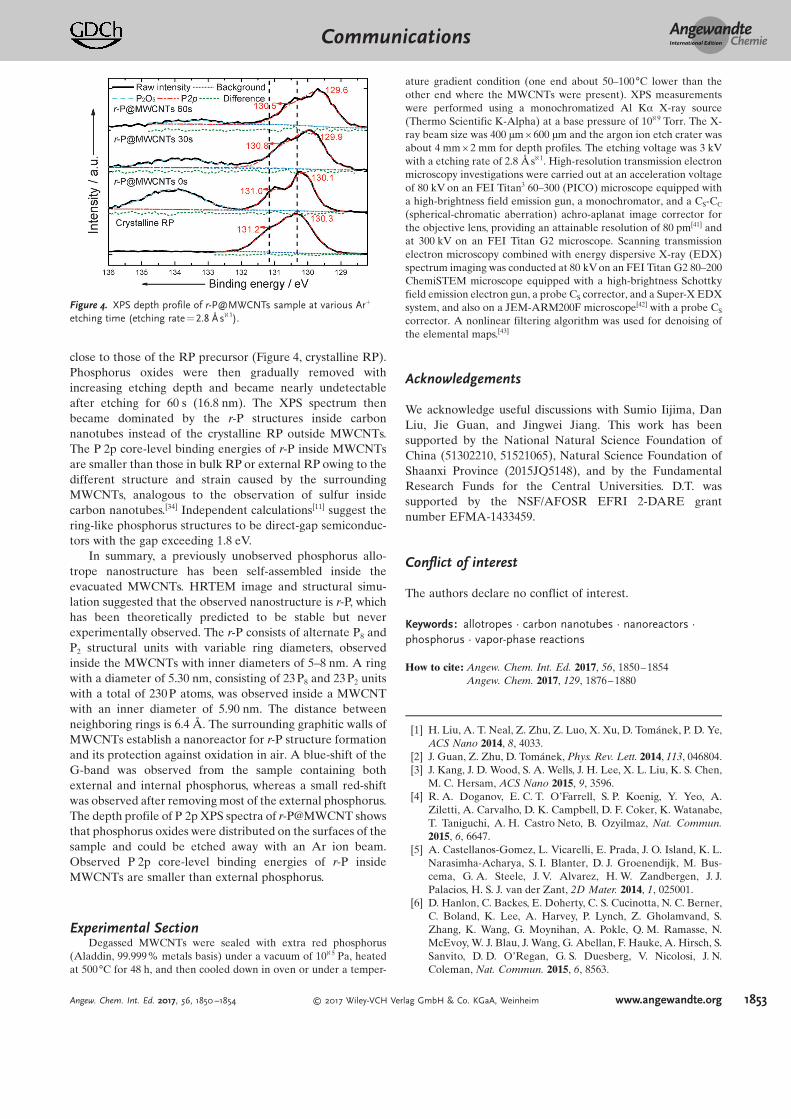
close to those of the RP precursor (Figure 4, crystalline RP).Phosphorus oxides were then gradually removed withincreasing etching depth and became nearly undetectableafter etching for 60 s (16.8 nm). The XPS spectrum thenbecame dominated by the r-P structures inside carbonnanotubes instead of the crystalline RP outside MWCNTs.The P 2p core-level binding energies of r-P inside MWCNTsare smaller than those in bulk RP or external RP owing to thedifferent structure and strain caused by the surroundingMWCNTs, analogous to the observation of sulfur insidecarbon nanotubes.[34] Independent calculations[11] suggest thering-like phosphorus structures to be direct-gap semiconduc-tors with the gap exceeding 1.8 eV.
In summary, a previously unobserved phosphorus allo-trope nanostructure has been self-assembled inside theevacuated MWCNTs. HRTEM image and structural simu-lation suggested that the observed nanostructure is r-P, whichhas been theoretically predicted to be stable but neverexperimentally observed. The r-P consists of alternate P8 andP2 structural units with variable ring diameters, observedinside the MWCNTs with inner diameters of 5–8 nm. A ringwith a diameter of 5.30 nm, consisting of 23 P8 and 23 P2 unitswith a total of 230 P atoms, was observed inside a MWCNTwith an inner diameter of 5.90 nm. The distance betweenneighboring rings is 6.4 c. The surrounding graphitic walls ofMWCNTs establish a nanoreactor for r-P structure formationand its protection against oxidation in air. A blue-shift of theG-band was observed from the sample containing bothexternal and internal phosphorus, whereas a small red-shiftwas observed after removing most of the external phosphorus.The depth profile of P 2p XPS spectra of r-P@MWCNT showsthat phosphorus oxides were distributed on the surfaces of thesample and could be etched away with an Ar ion beam.Observed P 2p core-level binding energies of r-P insideMWCNTs are smaller than external phosphorus.
Experimental SectionDegassed MWCNTs were sealed with extra red phosphorus
(Aladdin, 99.999% metals basis) under a vacuum of 10@5 Pa, heatedat 500 88C for 48 h, and then cooled down in oven or under a temper-
ature gradient condition (one end about 50–100 88C lower than theother end where the MWCNTs were present). XPS measurementswere performed using a monochromatized Al Ka X-ray source(Thermo Scientific K-Alpha) at a base pressure of 10@9 Torr. The X-ray beam size was 400 mm X 600 mm and the argon ion etch crater wasabout 4 mm X 2 mm for depth profiles. The etching voltage was 3 kVwith a etching rate of 2.8 c s@1. High-resolution transmission electronmicroscopy investigations were carried out at an acceleration voltageof 80 kV on an FEI Titan3 60–300 (PICO) microscope equipped witha high-brightness field emission gun, a monochromator, and a CS-CC
(spherical-chromatic aberration) achro-aplanat image corrector forthe objective lens, providing an attainable resolution of 80 pm[41] andat 300 kV on an FEI Titan G2 microscope. Scanning transmissionelectron microscopy combined with energy dispersive X-ray (EDX)spectrum imaging was conducted at 80 kV on an FEI Titan G2 80–200ChemiSTEM microscope equipped with a high-brightness Schottkyfield emission electron gun, a probe CS corrector, and a Super-X EDXsystem, and also on a JEM-ARM200F microscope[42] with a probe CS
corrector. A nonlinear filtering algorithm was used for denoising ofthe elemental maps.[43]
Acknowledgements
We acknowledge useful discussions with Sumio Iijima, DanLiu, Jie Guan, and Jingwei Jiang. This work has beensupported by the National Natural Science Foundation ofChina (51302210, 51521065), Natural Science Foundation ofShaanxi Province (2015JQ5148), and by the FundamentalResearch Funds for the Central Universities. D.T. wassupported by the NSF/AFOSR EFRI 2-DARE grantnumber EFMA-1433459.
Conflict of interest
The authors declare no conflict of interest.
Keywords: allotropes · carbon nanotubes · nanoreactors ·phosphorus · vapor-phase reactions
How to cite: Angew. Chem. Int. Ed. 2017, 56, 1850–1854Angew. Chem. 2017, 129, 1876–1880
[1] H. Liu, A. T. Neal, Z. Zhu, Z. Luo, X. Xu, D. Tom#nek, P. D. Ye,ACS Nano 2014, 8, 4033.
[2] J. Guan, Z. Zhu, D. Tom#nek, Phys. Rev. Lett. 2014, 113, 046804.[3] J. Kang, J. D. Wood, S. A. Wells, J. H. Lee, X. L. Liu, K. S. Chen,
M. C. Hersam, ACS Nano 2015, 9, 3596.[4] R. A. Doganov, E. C. T. OQFarrell, S. P. Koenig, Y. Yeo, A.
Ziletti, A. Carvalho, D. K. Campbell, D. F. Coker, K. Watanabe,T. Taniguchi, A. H. Castro Neto, B. Ozyilmaz, Nat. Commun.2015, 6, 6647.
[5] A. Castellanos-Gomez, L. Vicarelli, E. Prada, J. O. Island, K. L.Narasimha-Acharya, S. I. Blanter, D. J. Groenendijk, M. Bus-cema, G. A. Steele, J. V. Alvarez, H. W. Zandbergen, J. J.Palacios, H. S. J. van der Zant, 2D Mater. 2014, 1, 025001.
[6] D. Hanlon, C. Backes, E. Doherty, C. S. Cucinotta, N. C. Berner,C. Boland, K. Lee, A. Harvey, P. Lynch, Z. Gholamvand, S.Zhang, K. Wang, G. Moynihan, A. Pokle, Q. M. Ramasse, N.McEvoy, W. J. Blau, J. Wang, G. Abellan, F. Hauke, A. Hirsch, S.Sanvito, D. D. OQRegan, G. S. Duesberg, V. Nicolosi, J. N.Coleman, Nat. Commun. 2015, 6, 8563.
Figure 4. XPS depth profile of r-P@MWCNTs sample at various Ar+
etching time (etching rate=2.8 b s@1).
AngewandteChemieCommunications
1853Angew. Chem. Int. Ed. 2017, 56, 1850 –1854 T 2017 Wiley-VCH Verlag GmbH & Co. KGaA, Weinheim www.angewandte.org
[7] G. Abell#n, V. Lloret, U. Mundloch, M. Marcia, C. Neiss, A.Goerling, M. Varela, F. Hauke, A. Hirsch, Angew. Chem. Int. Ed.2016, 55, 14557; Angew. Chem. 2016, 128, 14777.
[8] J. Guan, Z. Zhu, D. Tom#nek, Phys. Rev. Lett. 2014, 113, 226801.[9] Z. Zhu, D. Tom#nek, Phys. Rev. Lett. 2014, 112, 176802.
[10] A. J. Karttunen, M. Linnolahti, T. A. Pakkanen, Chem. Eur. J.2007, 13, 5232.
[11] D. Liu, J. Guan, J. Jiang, D. Tom#nek, Nano Lett. 2016, 16, 7865.[12] J. W. Hittorf, Ann. Phys. 1865, 202, 193.[13] M. Ruck, D. Hoppe, B. Wahl, P. Simon, Y. K. Wang, G. Seifert,
Angew. Chem. Int. Ed. 2005, 44, 7616; Angew. Chem. 2005, 117,7788.
[14] J. L. Zhang, S. Zhao, C. Han, Z. Wang, S. Zhong, S. Sun, R. Guo,X. Zhou, C. D. Gu, K. D. Yuan, Z. Li, W. Chen, Nano Lett. 2016,16, 4903.
[15] A. H. Woomer, T. W. Farnsworth, J. Hu, R. A. Wells, C. L.Donley, S. C. Warren, ACS Nano 2015, 9, 8869.
[16] P. Yasaei, B. Kumar, T. Foroozan, C. H. Wang, M. Asadi, D.Tuschel, J. E. Indacochea, R. F. Klie, A. Salehi-Khojin, Adv.Mater. 2015, 27, 1887.
[17] R. Hultgren, N. S. Gingrich, B. E. Warren, J. Chem. Phys. 1935, 3,351.
[18] A. N. Khlobystov, ACS Nano 2011, 5, 9306.[19] J. Zhang, Y. Miyata, R. Kitaura, H. Shinohara, Nanoscale 2011,
3, 4190.[20] J. Zhang, Z. Zhu, Y. Feng, H. Ishiwata, Y. Miyata, R. Kitaura,
J. E. P. Dahl, R. M. K. Carlson, N. A. Fokina, P. R. Schreiner, D.Tom#nek, H. Shinohara, Angew. Chem. Int. Ed. 2013, 52, 3717;Angew. Chem. 2013, 125, 3805.
[21] J. Zhang, Y. Feng, H. Ishiwata, Y. Miyata, R. Kitaura, J. E. P.Dahl, R. M. K. Carlson, H. Shinohara, D. Tom#nek, ACS Nano2012, 6, 8674.
[22] A. Botos, J. Biskupek, T. W. Chamberlain, G. A. Rance, C. T.Stoppiello, J. Sloan, Z. Liu, K. Suenaga, U. Kaiser, A. N.Khlobystov, J. Am. Chem. Soc. 2016, 138, 8175.
[23] A. Chuvilin, E. Bichoutskaia, M. C. Gimenez-Lopez, T. W.Chamberlain, G. A. Rance, N. Kuganathan, J. Biskupek, U.Kaiser, A. N. Khlobystov, Nat. Mater. 2011, 10, 687.
[24] J. H. Warner, Y. Ito, M. H. Ruemmeli, T. Gemming, B. Buech-ner, H. Shinohara, G. A. D. Briggs, Phys. Rev. Lett. 2009, 102,195504.
[25] D. A. Britz, A. N. Khlobystov, K. Porfyrakis, A. Ardavan,G. A. D. Briggs, Chem. Commun. 2005, 37.
[26] L. Guan, K. Suenaga, S. Okubo, T. Okazaki, S. Lijima, J. Am.Chem. Soc. 2008, 130, 2162.
[27] L. H. Guan, K. Suenaga, S. Iijima, Nano Lett. 2008, 8, 459.[28] X. Li, Z. Wang, J. Zhang, C. Xie, B. Li, R. Wang, J. Li, C. Niu,
Carbon 2015, 85, 168.[29] K. Kamalasanan, R. Gottardi, S. Tan, Y. Chen, B. Godugu, S.
Rothstein, A. C. Balazs, A. Star, S. R. Little, Angew. Chem. Int.Ed. 2013, 52, 11308; Angew. Chem. 2013, 125, 11518.
[30] J. X. Xu, L. H. Guan, RSC Adv. 2013, 3, 5577.[31] J. Zhang, F. Zhou, Y. Miyata, R. Kitaura, H. Su, H. Shinohara,
RSC Adv. 2014, 3, 16954.[32] C. L. Jia, M. Lentzen, K. Urban, Science 2003, 299, 870.[33] C. L. Jia, L. Houben, A. Thust, J. Barthel, Ultramicroscopy 2010,
110, 500.[34] T. Fujimori, A. Morelos-Gomez, Z. Zhu, H. Muramatsu, R.
Futamura, K. Urita, M. Terrones, T. Hayashi, M. Endo, S. Y.Hong, Y. C. Choi, D. Tomanek, K. Kaneko, Nat. Commun. 2013,4, 2162.
[35] T. Fujimori, R. B. dos Santos, T. Hayashi, M. Endo, K. Kaneko,D. Tomanek, ACS Nano 2013, 7, 5607.
[36] A. Pfitzner, M. F. Brau, J. Zweck, G. Brunklaus, H. Eckert,Angew. Chem. Int. Ed. 2004, 43, 4228; Angew. Chem. 2004, 116,4324.
[37] K. Nakamoto, Infrared and Raman Spectra Of Inorganic AndCoordination Compounds Part A, 6th ed., Wiley, Hoboken,2009, p. 177.
[38] A. C. Ferrari, Solid State Commun. 2007, 143, 47.[39] A. Das, S. Pisana, B. Chakraborty, S. Piscanec, S. K. Saha, U. V.
Waghmare, K. S. Novoselov, H. R. Krishnamurthy, A. K. Geim,A. C. Ferrari, A. K. Sood, Nat. Nanotechnol. 2008, 3, 210.
[40] R. Voggu, C. S. Rout, A. D. Franklin, T. S. Fisher, C. N. R. Rao, J.Phys. Chem. C 2008, 112, 13053.
[41] J. Barthel, L. Houben, K. Tillmann, JLSRF 2015, 1, A34.[42] A. Kov#cs, R. Schierholz, K. Tillmann, JLSRF 2016, 2, A43.[43] H. C. Du, Ultramicroscopy 2015, 151, 62.
Manuscript received: December 2, 2016Final Article published: January 11, 2017
AngewandteChemieCommunications
1854 www.angewandte.org T 2017 Wiley-VCH Verlag GmbH & Co. KGaA, Weinheim Angew. Chem. Int. Ed. 2017, 56, 1850 –1854