compact and high isolation microstrip diplexer for ... · pdf filecompact and high isolation...
TRANSCRIPT

Progress In Electromagnetics Research, Vol. 133, 555–570, 2013
COMPACT AND HIGH ISOLATION MICROSTRIPDIPLEXER FOR BROADBAND AND WLAN APPLICA-TION
H. W. Deng*, Y. J. Zhao, Y. Fu, J. Ding, and X. J. Zhou
College of Electronic and Information Engineering, Nanjing Universityof Aeronautics and Astronautics, Nanjing 210016, China
Abstract—In this paper, a compact and high isolation microstripdiplexer is designed for broadband and wireless local area network(WLAN) application, simultaneously. The bandpass filter (BPF) forbroadband channel is formed by three-coupled-line structure and twoshort stubs with different size loaded in 50 Ω feed lines, and theBPF for WLAN channel consists of two coupling quarter-wavelengthresonators (QWR) and one open stub loaded in short parallel-couplingfeed structure. Multiple transmission zeros can be generated dueto their intrinsic characteristics, so the broadband BPF with sharpskirt and wide upper-stopband performance and the WLAN BPF withsharp roll-off and lower-stopband characteristic can be realized. Thetapped stub not only can generate new transmission zeros to deepenthe stopband, but also can connect other BPF as an its part withoutdeterioration of in-band performance. Hence, a compact microstripdiplexer combines of two BPFs without the extra junction matchingnetwork. The mutual loading effect approximately equivalent to acoupled QWR can also generate new transmission zero at the passbandedge to improve the isolation. A microstrip diplexer with the 3 dBfractional bandwidths (FBW) of 80% for broadband channel and5% for WLAN channel is designed and fabricated. Good agreementbetween the simulated and measured results is observed.
1. INTRODUCTION
A diplexer, as an essential component in multi-service and multi-bandcommunication systems, is a three-terminal device which lets two ormore frequencies into one input port and then separating them to two
Received 23 September 2012, Accepted 5 November 2012, Scheduled 8 November 2012* Corresponding author: Hong Wei Deng ([email protected]).

556 Deng et al.
other output ports. A well designed diplexer should have low cost andhigh performance. Microstrip diplexers as low cost ones can be easilymounted on the dielectric substrate and can provide a more flexibledesign of the circuit layout [1]. Hence, microstrip diplexers were widelystudied in the early 1960s by Matthaei et al. [2] and Wenzel [3]. Inthe past few years, much effort on the microstrip diplexer has beenpaid to reduce the size and improve the performance. Due to theinteraction of two filters composing the diplexer, the characteristics ofa microstrip diplexer are different from the responses of the individualtwo microstrip filters. The complexity of the interaction makes thedesign of a microstrip diplexer complicated [4].
For the design of microstrip diplexers, the traditional approachis to design the two different filters individually and then to designa matching circuit. The most intuitive approach is to combine twoBPFs with a T-junction or Y-junction [5–10]. The method, whichfeatures the filter A (filter B) an open-circuit-load shunted to the filterB (filter A) at the frequency of the latter, is adopted to figure thedimensions of the connecting line for reducing the mutual loadingeffect between the filters. Owing to the well development of theBPF implementation [11, 12], it is relatively easy to design decentdiplexers based on this approach. This kind of diplexers, however,usually occupies a considerable footprint due to the required large sizefrom the junction. In [13–16], the common resonator technology isproposed to remove the input junction in the diplexer designs andreduces the size to a large degree. However, since the passbandsof the diplexer rely on the first two resonant frequencies of thecommon resonator, the common resonator needs to be chosen properly.Some interesting diplexer designs without distribution networks haveappeared in the recent literatures [17–21]. A new topology of thediplexer with the common port directly connected to two filters wasproposed and synthesized in [17], although no design example wasgiven. A design procedure for coupled resonator diplexers that doesnot employ any external junctions was also reported in [18], and wasfurther verified in [19]. In addition, the composite right/left-handedtransmission lines [20] and substrate integrated waveguide (SIW) withcomplementary split-ring resonators [21] can be applied to the diplexerdesigns, which do not require matching network. Despite compactdiplexers can be obtained, isolation and insertion loss of these diplexersare not satisfactory.
Furthermore, broadband or ultra-wideband (UWB) moderncommination systems [22–25] have promoted the development of themicrostrip diplexer with broadband channel. But there are fewliteratures until now concerning microstrip diplexer with broadband

Progress In Electromagnetics Research, Vol. 133, 2013 557
or UWB application. In a previous work [26], a microstrip diplexer forBluetooth and UWB application is presented by combining two ring-like BPFs with tapped T-junction coupling line. A UWB microstripdiplexer in [27] is formed by two hairpin line filtering structures withoutthe matching network and a tapped open stub used to introduce anattenuation pole to suppress the spurious response. However, the abovementioned diplexers [26, 27] in fact have the drawbacks such as lowisolation and large dimension.
In this paper, a compact and high isolation microstrip diplexerfor broadband and WLAN [28, 29] application is designed throughthe combination of two BPFs without the extra junction matchingnetwork. The BPF for broadband channel is formed by three-coupled-line structure and two short stubs with different size loaded in 50Ω feedlines, and the BPF for WLAN channel consists of two coupling QWRsand one open stub loaded in short parallel-coupling feed structure.Multiple transmission zeros can be created to achieve high out-bandrejection of two filters owing to their intrinsic characteristics. Thetapped stub connects other high out-band rejection BPF as an itspart without deterioration of in-band performance. Because of thecoupling between the tapped stub and the QWR, new transmissionzero can be created at the other channel passband edge to improve theisolation. Finally, a microstrip diplexer is designed and fabricated, anda satisfactory agreement between the simulated and measured resultsvalidates the proposed configuration.
2. HIGH ISOLATION MICROSTRIP DIPLEXER DESIGN
2.1. Analysis of the Uniform Resonator Coupling TappedStub
As well-known, the stub loaded in the 50Ω feed lines can be applied togenerate new transmission zeros. And the transmission zeros generatedby the open stub and short stub can be expressed as, respectively:
fopen = nc/ (4√
εe l) ; fshort = nc/ (2√
εe l) , (1)
where l refers to the length of the stub, c the speed of light, and εe theequivalent dielectric constant.
Furthermore, the effects of the coupled different end uniformresonators on the open and short tapped stubs are investigated. Thecurrent distributions of six different cases are simulated by HFSS andshown in Figure 1. The substrate used is RT/Duroid 5880 with athickness of 0.508 mm, permittivity of 2.2 and loss tangent 0.0009. Wecan directly see that only the currents of the short uniform resonator

558 Deng et al.
(a) (b)
(c) (d)
(e) (f)
w
d1opentappedstub
openuniformresonator
d2
g
50 Ω
w
d 1opentappedstub
shortuniformresonator
d 2
g
50 Ω
w
d 1opentappedstub
shortuniformresonator
d 2
g
50 Ω
w
d 1shorttappedstub
openuniformresonator
d 2
g
50 Ω
wd 1
shorttappedstub
shortuniformresonator
d 2
g
50 Ω
w
d 1shorttappedstub
shortuniformresonator
d 2
g
50 Ω
Figure 1. Current distributions at 5 GHz of the different end uniformresonator coupling open and short tapped stubs. (The structuralparameters are: d1 = 15 mm; d2 = 13mm; w = 0.3mm; g = 0.1mm).
in Figures 1(c) and (e) are very strong distribution, but the currentdistribution in Figure 1(c) is strongest.

Progress In Electromagnetics Research, Vol. 133, 2013 559
T
|S| i
n dB
The open tapped stub The structure in Fig.1(a) The structure in Fig.1(b) The structure in Fig.1(c)
T
T
T|S| i
n dB
The short tapped stub The strcture in Fig.1(d) The strcture in Fig.1(e) The strcture in Fig.1(f)
0
-5-10
-15
-20
-25-30
-35
-40-45
21
0 1 2 3 4 5 6 7 8 9 10
0
-5
-10
-15
-20
-25
-30
-35
-40
21
0 1 2 3 4 5 6 7 8 9 10Frequency (GHz) Frequency (GHz)
z1
z2
z3
z4
(a) (b)
Figure 2. The |S21| in dB of the different end uniform resonatorcoupling tapped stubs. (a) Open tapped stub. (b) Short tapped stub.
T
the open tapped stub g=0.1 mm g=0.2 mm g=0.3 mm g=0.4 mm
T T
the short tapped stub g=0.1 mm g=0.2 mm g=0.3 mm g=0.4 mm
T
|S| i
n dB
0
-5
-10
-15-20
-25-30
-35-40
-45
21
0 1 2 3 4 5 6 7 8 9 10Frequency (GHz)
|S| i
n dB
0
-5
-10
-15
-20
-25
-30
-35
-40
-45
21
0 1 2 3 4 5 6 7 8 9 10Frequency (GHz)
z1
z2
z4
z3
(a) (b)
Figure 3. The simulated |S21| in dB with varied g. (a) The couplingopen tapped stubs in Figure 1(c). (b) The coupling short tapped stubsin Figure 1(e).
The |S21| in dB of the different end uniform resonator couplingtapped stubs in the range of 0.1–10 GHz are interpreted in Figure 2.The uniform resonators in the structures in Figures 1(a), (b), (d)and (f) have less effect on the first transmission zero created bythe tapped stub and cannot generate new transmission zero, for themutual coupling between the uniform resonator and the tapped stubis very weak. But the short uniform resonators in the structures inFigures 1(c) and (e) can generate new transmission zeros Tz2 andTz4, respectively. As the gap g decreased, the transmission zeroTz2 approximately equal to c/(4
√εed2)GHz moves towards upper
frequency, as shown in Figure 3(a), whereas the transmission zero Tz1
created by the open tapped stub moves downwards. We can see that

560 Deng et al.
Source load
I
I
II
II
V V
V VV
V
Z ZZ
θ θ θ000
000
544
321
321
56
6
Figure 4. General equivalent circuit of the symmetric three-coupled-line structure.
the transmission zero Tz4 in Figure 3(b) mainly determined by theshort uniform resonator is located at c/(4
√εed2)GHz, whereas the
transmission zero Tz3 created by the short tapped stub basically keepsunchanged. Hence, the structures in Figures 1(c) and (e) may beapplied to improve the sharp skirt and wide stopband performance ofthe microstrip filter.
2.2. Sharp Skirt and Wide Upper-stopband Broadband BPFwith Two Different Size Tapped Stubs
The broadband BPF is designed by using symmetric three-coupled-line structure composed of a QWR side-coupled to two open stubs.Figure 4 depicts the general equivalent circuit of the structure withthe termination conditions given by the following equations:
V5 = 0; I2 = I4 = I6 = 0, (2)
Thus, a simple analysis based on a transmission line model canbe employed to investigate its filtering characteristics. As explainedin [30], the parameters of three-coupled-line structure are completelyobtained in terms of the static capacitance matrix with the dielectric inplace and removed. Based on the analysis in [30, 31], the structure canproduce three resonant modes, and the center frequency and passbandbandwidth are mainly determined by the electrical length θ0 of theQWR and the coupling gap, respectively.
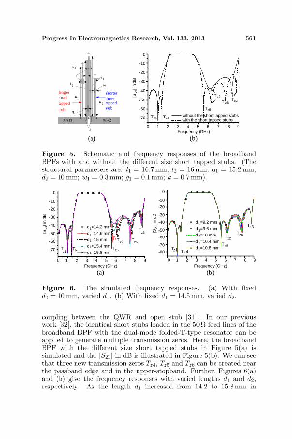
To obtain a big 3 dB FBW, the BPF designed by using thestructure with tight coupling in Figure 5(a) is simulated and optimizedby HFSS. The simulated frequency responses in the range of 0.1–9GHz are interpreted in Figure 5(b). The filter has three transmissionzeros Tz1, Tz2 and Tz3 at the lower- and upper-stopbands, which aregenerated by the cross coupling between two open stubs and the
Progress In Electromagnetics Research, Vol. 133, 2013 561
T
T TT
T
without the short tapped stubs with the short tapped stubs
T
w
d1short
tapped
stub
d2
50 Ω
1
l1l 2
longer
shortshorter
tappedstub
1g
50 Ω
k
0
-10
-20
-30
-50
-40
-60
0 1 2 3 4 5 6 7 8 9Frequency (GHz)
-70
|S| i
n dB
21(a) (b)
z1
z2
z4
z3
z5
z6
w1
Figure 5. Schematic and frequency responses of the broadbandBPFs with and without the different size short tapped stubs. (Thestructural parameters are: l1 = 16.7mm; l2 = 16 mm; d1 = 15.2mm;d2 = 10 mm; w1 = 0.3mm; g1 = 0.1mm; k = 0.7mm).
T
TT
T
T
d =14.2 mm
d =14.6 mm
d =15 mm
d =15.4 mm
d =15.8 mmT
T
T
T
T
T
d =9.2 mm
d =9.6 mm
d =10 mm
d =10.4 mm
d =10.8 mmT
0
-10
-20
-30
-50
-40
-60
0 1 2 3 4 5 6 7 8 9Frequency (GHz)
-70
|S| i
n dB
21
(a) (b)
0
-10
-20
-30
-50
-40
-60
-70
|S| i
n dB
21
-80
0 1 2 3 4 5 6 7 8 9Frequency (GHz)
z1
z2
z4
z3
z5
z6
z1
z2
z5
z6
z3
z4
1
1
1
1
1
2
2
2
2
2
Figure 6. The simulated frequency responses. (a) With fixedd2 = 10 mm, varied d1. (b) With fixed d1 = 14.5mm, varied d2.
coupling between the QWR and open stub [31]. In our previouswork [32], the identical short stubs loaded in the 50 Ω feed lines of thebroadband BPF with the dual-mode folded-T-type resonator can beapplied to generate multiple transmission zeros. Here, the broadbandBPF with the different size short tapped stubs in Figure 5(a) issimulated and the |S21| in dB is illustrated in Figure 5(b). We can seethat three new transmission zeros Tz4, Tz5 and Tz6 can be created nearthe passband edge and in the upper-stopband. Further, Figures 6(a)and (b) give the frequency responses with varied lengths d1 and d2,respectively. As the length d1 increased from 14.2 to 15.8 mm in

562 Deng et al.
Figure 6(a), the transmission zeros Tz1, Tz2, Tz3 and Tz6, specially thetransmission zeros Tz2 and Tz6, move towards the lower frequency, butthe transmission zero Tz5 near the passband edge shifts upwards. Thetransmission zeros in Figure 6(b) remain almost unchanged, except theTz6 moves towards the lower frequency, while changing the length d2
from 9.2 to 10.8mm. Thus, a compact broadband BPF can be realizedwith sharp skirt and deep stopband performance by simply adjustingthe lengths d1 and d2.
2.3. Sharp Skirt and Wide Lower-stopband BPF withTapped Stub
As shown in Figure 7(a), the BPF for WLAN application consists oftwo coupling QWRs, denoted by the length l1 + l2 + l3 and width w1,and short microstrip feedlines (k1 + k2, w1). The passband frequencydepends on the electrical length of the resonator. External qualityfactors and coupling coefficients are determined by the gap g1 andthe length k2. The frequency responses with varied k2 are simulatedin the range of 0.1–11 GHz and interpreted in Figure 7(b). We cansee that two transmission zeros Tz1 and Tz2 can be generated nearthe passband edge. As explained in [33], the short feedline can controlsource-load coupling easily to produce an equivalent feedback capacitorbetween I/O ports. Hence, the transmission zero Tz2 created by thesource-load coupling moves towards the passband edge, whereas thein-band and lower-stopband performance remain almost unchanged,as the length k2 increased. But the length k2 need to be reasonably
T
T k =6.5mm
k =7.5mm
k =8.5mm
0
-10
-20
-30
-50
-40
-60
0 1 2 3 4 5 6 7 8 9Frequency (GHz)
-70
|S| i
n dB
21
(a) (b)
10 11
z2
2
2
2
k
50 Ω
2
l3l 2
source-load
via hole
coupling
2g
k
w1
via hole
50 Ω1
1g
z1
Figure 7. Schematic of the BPF in [33] and frequency responses withvaried k2. (The structural parameters are: l1 = 3.0mm; l2 = 5.0mm;l3 = 1.9 mm; k1 = 5.0mm; g1 = 0.22mm; g2 = 0.8mm; w1 = 0.3mm).

Progress In Electromagnetics Research, Vol. 133, 2013 563
T
T
T
k =22 mm
k =23 mm
k =24 mm
without the open tapped stub
T
0
-10
-20
-30
-50
-40
-60
0 1 2 3 4 5 6 7 8 9Frequency (GHz)
-70
|S| i
n dB
21
(b)
z1
z2
z3
z4
(a)
k
50 Ω
3
l 3l2
2g
k
w 1
50 Ω11g
k2
k
w1
33
3
Figure 8. Schematic of the BPF with one open tapped stub and thefrequency responses with varied k3, fixed k = 1.0mm.
chosen to obtain sharp skirt and compact size. Meanwhile, the filterwith very deep lower-stopband performance can be realized, for theQWR has no resonate mode in lower-stopband.
Furthermore, the filter with one open stub with the length k3 andwidth w1 loaded in the 50 Ω feed line is simulated and compared inFigure 8. Two transmission zeros Tz3 and Tz4 created by the opentapped stub can be adjusted in the lower-stopband and near the upperpassband edge, which sharpen the skirt and deepen the stopband.However, the center frequency shifts downwards and the bandwidthbecome narrower. So the length l1 + l2 + l3 and the gaps g1, g2 needto be simply readjusted to obtain desired in-band performance.
2.4. High Isolation Microstrip Diplexer for Broadband andWLAN Application
Based on the features of the aforementioned sharp skirt and wideupper-stopband broadband BPF with two different size short tappedstub in Figure 5(a) and sharp skirt and wide lower-stopband BPFwith open tapped stub in Figure 8(a), a microstrip diplexer, as shownin Figure 9, may be designed through the combination of two filters.As a filter part, the longer short tapped stub in Figure 5(a) and opentapped stub in Figure 8(a) are directly connected to common portwithout extra junction matching network, so more compact size canalso be realized.
The mutual loading effect of two filters can be further investigated.The broadband filter with coupling short tapped stub and WLANfilter with coupling open tapped stub, as shown in Figure 10, are

564 Deng et al.
port 1
port 2 port 350 Ω 50 Ω
50 Ω
k3l3 l 2
2g
k
w1
1
1g
kkd2
w1
l1
4 3g 3d
k2d1
Figure 9. Schematic of the microstrip diplexer for GPS and WLANapplication. (The structural parameters are: l1 = 16.7mm; l2 =16mm; l3 = 10 mm; w1 = 0.3mm; d1 = 3.0mm; d2 = 5.0mm;d3 = 1.9mm; k = 0.7mm; k1 = k4 = 2.22mm; k2 = 5.0mm;k3 = 7.5mm; g1 = 0.1mm; g2 = 0.22mm; g3 = 0.8mm).
(a) (b)
port 1
port 2 port 350 Ω 50 Ω
port 1 50 Ω
50 Ω
short tappedstub
coupling shorttapped stub
coupling
tappedopen
stub
tappedopen
stub
Figure 10. Configurations of the broadband filter with (a) thecoupling short tapped stub and (b) the WLAN filter with the couplingopen tapped stub.
simulated by HFSS, respectively. Figure 11 and Figure 12 give thesimulated insertion losses of the broadband filter with coupling shorttapped stub and WLAN filter with coupling open tapped stub. Asdiscussed in Section 2.1, the QWRs in coupling short tapped stub andcoupling open tapped stub can generate new transmission zeros Tz7
and Tz4, respectively. Compared to the broadband filter with shorttapped stub and WLAN filter with open tapped stub, only differenceis that the transmission zeros Tz2 and Tz5, near the transmission zero

Progress In Electromagnetics Research, Vol. 133, 2013 565
TT
broadband filter with short tapped stub broadband filter with coupling short tapped stub broadband channel
T
0
-10
-20
-30
-50
-40
-60
0 1 2 3 4 5 6 7 8 9Frequency (GHz)
-70
|S| i
n dB
21
-80
-90
z2z7
z5
Figure 11. The |S21| in dB of thebroadband filter with the couplingshort tapped stub and broadbandchannel of the diplexer.
T
WLAN filter with open tapped stub
WLAN filter with coupling open tapped stub
WLAN channel
T
0
-10
-20
-30
-50
-40
-60
0 1 2 3 4 5 6 7 8 9Frequency (GHz)
-70
|S| i
n dB
31
-80
z4z3
Figure 12. The |S21| in dBof the WLAN filter with thecoupling open tapped stub andWLAN channel of the diplexer.
Figure 13. Photograph of the implemented proposed microstripdiplexer.
Tz7, and the transmission zero Tz3, near the transmission zero Tz4, arereadjusted. Meanwhile, we can see from the Figure 11 and Figure 12that the insertion losses of the broadband filter with coupling shorttapped stub and WLAN filter with coupling open tapped stub showa better agreement with the corresponding channel in the diplexer.So, the mutual loading effect approximately equivalent to a coupledQWR can generate one new transmission zero at the passband edge toimprove the isolation. Meanwhile, the compact diplexer remains thelow insertion loss and high selective characteristics of two filters. Tovalidate the design approach, the diplexer with 3 dB FBWs of 80% at3.0GHz for broadband channel and 5% at 5.8GHz for WLAN channelis simulation and optimization by HFSS, and the dimensions are listedin Figure 9.

566 Deng et al.
3. EXPERIMENTAL RESULTS
After studying the characteristics of the microstrip diplexer forbroadband and WLAN application, the diplexer is fabricated on theDuroid 5880 substrate and its photogragh is shown in Figure 13.The filtering performance is measured by Agilent network analyzerN5230A. The simulated and measured frequency responses are shownin Figure 14, and illustrated good agreement. The losses and theslight shift in the center frequencies are attributed to manufacturingtolerances. The measured 3 dB FBWs are 80.3% at 3GHz forbroadband channel and 3.45% at 5.8 GHz for WLAN channel, withmeasured minimum insertion losses are −3 dB and the passband returnloss better than −10.3 dB. Two transmission zeros near the broadbandpassband edge are located at 1.38GHz and 5.65GHz resulting in
S
S
Simulated Measured
S Simulated Measured
Simulated Measured
Simulated Measured
0-10
-20
-30
-50
-40
-60
0 1 2 3 4 5 6 7 8 9Frequency (GHz)
-70
|S| i
n dB
32
-80
-90
|S| i
n dB
31|S
| ,21
|S| ,
11
0-10
-20
-30
-50
-40
-60
0 1 2 3 4 5 6 7 8 9Frequency (GHz)
-70
-80
-90
1.0
0.9
0.8
0.7
0.5
0.6
0.4
1.5 2.0 2.5 3.0 3.5 4.0 4.5 5.0Frequency (GHz)
0.3
0.2
Gro
up d
elay
(ns
)
2.4
2.0
1.6
1.2
0.4
0.8
0.0
-0.46.1
Gro
up d
elay
(ns
)
5.3 5.4 5.5 5.6 5.7 5.8 5.9 6.0 6.2 6.46.3 6.5Frequency (GHz)
(a) (b)
(c) (d)
11 31
21
Figure 14. The simulated and measured frequency responses of themicrostrip diplexer. (a) |S11|, |S21|, |S31| in dB. (b) |S32| in dB.(c) Group delay of the broadband channel. (d) Group delay of theWLAN channel.

Progress In Electromagnetics Research, Vol. 133, 2013 567
sharp skirt, with an attenuation level of more than 59 dB. The upper-stopband of the broadband channel in experiment is extended up to8.68GHz with an insertion loss larger than 35 dB. The out-of-bandrejection level of the WLAN channel is better than 30 dB in the rangeof 0.1–5.36 GHz and 7.01–9 GHz. Meanwhile, the measured isolationgreater than 37.5 dB in broadband passband and more than 46 dB inWLAN passband, as shown in Figure 14(b), is achieved between twochannels. In addition, the measured in-band group delay for broadbandchannel and WLAN channel in Figure 14(c) and Figure 14(d) vary from0.3 to 0.6 ns and from 1.45 to 1.75 ns, respectively, which is quite smalland flat in the broadband and WLAN passbands. The size withoutthe 50Ω feed lines is only 0.266λ × 0.277λ in which λ is the guidedwavelength at 3 GHz.
4. CONCLUSION
In this paper, a novel compact, low insertion loss, sharp skirt and highisolation microstrip diplexer for broadband and WLAN application isproposed through the combination of two out-band rejection BPFswith the tapped stub without the extra junction matching network.Due to the intrinsic characteristics and mutual loading effect of twofilters, multiple transmission zeros can be generated to achieve sharpskirt, deep stopband and high isolation of the diplexer. Finally, amicrostrip diplexer with the 3 dB FBWs of 80% at 3GHz for broadbandchannel and 5% at 5.8GHz for WLAN channel is designed andfabricated. The good agreement between the simulated and measuredresults demonstrates the validity of our proposed structure.
ACKNOWLEDGMENT
This work was supported by the Priority Academic ProgramDevelopment of Jiangsu Higher Education Institutions (PAPD),Funding of Jiangsu Innovation Program for Graduate Education(No. CX10B 109Z) and Funding for Outstanding Doctoral Dissertationin NUAA (No. BCXJ10-06).
REFERENCES
1. Pozar, D. M., Microwave Engineering, Wiley, New York, 1998.2. Matthaei, G. and E. G. Cristal, “Multiplexer channel-separating
units using interdigital and parallel-coupled filters,” IEEETransactions on Microwave Theory and Techniques, Vol. 13, 328–334, 1965.

568 Deng et al.
3. Wenzel, R. J., “Printed-circuit complementary filters for narrowbandwidth multiplexers,” IEEE Transactions on MicrowaveTheory and Techniques, Vol. 16, 147–157, 1968.
4. Wang, R., J. Xu, M. Y. Wang, and Y. L. Dong, “Synthesis ofmicrostrip resonator diplexers using linear frequency transforma-tion and optimization,” Progress In Electromagnetics Research,Vol. 124, 441–455, 2012.
5. Yang, T., P. L. Chi, and T. Itoh, “High isolation and compactdiplexer using the hybrid resonators,” IEEE Microstrip andWireless Components Letters, Vol. 20, No. 10, 551–553, 2010.
6. Huang, C. Y., M. H. Weng, C. S. Ye, and Y. X. Xu, “A high bandisolation and wide stopband diplexer using dual-mode stepped-impedance resonators,” Progress In Electromagnetics Research,Vol. 100, 299–308, 2010.
7. Yang, R. Y., C. M. Hsiung, C. Y. Hung, and C. C. Lin,“Design of a high band isolation diplexer for GPS and WLANsystem using modified stepped-impedance resonators,” ProgressIn Electromagnetics Research, Vol. 107, 101–114, 2010.
8. Shi, J., J. X. Chen, and Z. H. Bao, “Diplexers based onmicrostrip line resonators with loaded elements,” Progress InElectromagnetics Research, Vol. 115, 423–439, 2011.
9. Zeng, H. Y., G. M. Wang, D. Z. Wei, and Y. W. Wang,“Planar diplexer using composite right-/left-handed transmissionline under balanced condition,” Electronics Letters, Vol. 48, No. 2,104–106, 2012.
10. Lin, Y.-L., S.-W. Lan, R.-Y. Yang, and C.-Y. Hung, “Designof a high band-isolation diplexer based on asymmetric stepped-impedance resonators with side-coupling structure,” Journal ofElectromagnetic Waves and Applications, Vol. 27, No. 1, 1–11,2012.
11. Chen, C.-Y. and C.-C. Lin, “The design and fabrication of ahighly compact microstrip dual-band bandpass filter,” ProgressIn Electromagnetics Research, Vol. 112, 299–307, 2011.
12. Rezaee, P., M. Tayarani, and R. Knochel, “Active learningmethod for the determination of coupling factor and external Q inmicrostrip filter design,” Progress In Electromagnetics Research,Vol. 120, 459–479, 2011.
13. Chen, C. F., T. Y. Huang, C. P. Chou, and R. B. Wu, “Microstripdiplexers design with common resonator sections for compact size,but high isolation,” IEEE Transactions on Microwave Theory andTechniques, Vol. 54, No. 5, 1945–1952, 2006.
Progress In Electromagnetics Research, Vol. 133, 2013 569
14. Yang, T. P., L. Chi, and T. Itoh, “Compact quarter-wave resonator and its applications to miniaturized diplexerand triplexer,” IEEE Transactions on Microwave Theory andTechniques, Vol. 59, No. 2, 260–269, 2011.
15. Chuang, M. L. and M. T. Wu, “Microstrip diplexer design usingcommon T-shaped resonator,” IEEE Microwave and WirelessComponents Letters, Vol. 21, No. 11, 583–585, 2011.
16. Chen, C.-F., “Miniaturized and high isolation microstrip diplexersbased on the tri-mode stubloaded stepped-impedance resonators,”Journal of Electromagnetic Waves and Applications, Vol. 26,Nos. 14–15, 2001–2011, 2012.
17. Garcia-Lamperez, A., M. Salazar-Palma, and T. K. Sarkar,“Analytical synthesis of microwave multiport networks,” IEEEMTT-S Int. Microwave Symp. Digest, 455–458, 2004.
18. Skaik, T. F., M. J. Lancaster, and F. Huang, “Synthesis ofmultiple output coupled resonator circuits using coupling matrixoptimisation,” IET Microwaves, Antennas and Propagation,Vol. 5, No. 9, 1081–1088, 2011.
19. Skaik, T. F. and M. J. Lancaster, “Coupled resonator diplexerwithout external junctions,” Journal of Electromagnetic Analysisand Applications, Vol. 3, No. 6, 238–241, 2011.
20. An, J., G. M. Wang, C. X. Zhang, and P. Zhang, “Diplexerusing composite right-/left-handed transmission line,” ElectronicsLetters, Vol. 44, No. 11, 685–687, 2008.
21. Dong, Y. D. and T. Itoh, “Substrate integrated waveguide loadedby complementary split-ring resonators for miniaturized diplexerdesign,” IEEE Microwave and Wireless Components Letters,Vol. 21, No. 1, 10–12, 2011.
22. Quan, X. L., R.-L. Li, J. Y. Wang, and Y. H. Cui, “Developmentof a broadband horizontally polarized omnidirectional planar an-tenna and its array for base stations,” Progress In Electromagnet-ics Research, Vol. 128, 441–456, 2012.
23. Islam, M. T., R. Azim, and A. T. Mobashsher, “Triple band-notched planar UWB antenna using parasitic strips,” Progress InElectromagnetics Research, Vol. 129, 161–179, 2012.
24. Russo, I., L. Boccia, G. Amendola, and H. Schumacher, “Compacthybrid coaxial architecture for 3-10GHz UWB quasi-optical powercombiners,” Progress In Electromagnetics Research, Vol. 122, 77–92, 2012.
25. Azim, R. and M. T. Islam, “Compact planar UWB antenna withband notch characteristics for WLAN and DSRC,” Progress In
570 Deng et al.
Electromagnetics Research, Vol. 133, 391–406, 2013.26. Ye, C. S., Y. K. Su, M. H. Weng, and C. Y. Hung, “A microstrip
ring-like diplexer for bluetooth and UWB application,” Microwaveand Optical Technology Letters, Vol. 51, No. 6, 1518–1520, 2009.
27. Weng, M. H., C. Y. Hung, and Y. K. Su, “A hairpin line diplexerfor direct sequence ultra-wideband wireless communications,”IEEE Microwave and Wireless Components Letters, Vol. 17, No. 7,519–521, 2007.
28. Ma, D., Z. Y. Xiao, L. Xiang, X. Wu, C. Huang, and X.Kou, “Compact dual-band bandpass filter using folded SIR withtwo stubs for WLAN,” Progress In Electromagnetics Research,Vol. 117, 357–364, 2011.
29. Panda J. R. and R. S. Kshetrimayum, “A printed2.4GHz/5.8 GHz dual-band monopole antenna with a protrudingstub in the ground plane for WLAN and RFID applications,”Progress In Electromagnetics Research, Vol. 117, 425–434, 2011.
30. Nguyen, C. and K. Chang, “On the analysis and design of spurlineband-stop filters,” IEEE Transactions on Microwave Theory andTechniques, Vol. 33, No. 12, 1416–1421, 1985.
31. Song, K. and Q. Xue, “Novel broadband bandpass filters using Y-shaped dual-mode microstrip resonators,” IEEE Microwave andWireless Components Letters, Vol. 19, No. 9, 548–550, 2009.
32. Deng, H. W., Y. J. Zhao, X. S. Zhang, W. Chen, andL. Qiang, “Compact and high selectivity broadband bandpassfilter with dual-mode folded-T-type resonator,” Microwave andOptical Technology Letters, Vol. 53, No. 8, 1697–1700, 2011.
33. Dai, G. L., Y. X. Guo, and M. Y. Xia, “Design of compactbandpass filter with improved selectivity using source-loadcoupling,” Electronics Letters, Vol. 46, No. 7, 505–506, 2010.