compactflash™ bus-interface chip with ±15 … pin configurations to optimize pcb cf card...
TRANSCRIPT
Bus-Transceiver
Circuitry
CF4320H
Card-DetectCircuitry
±1
5-k
V H
BM
ES
D P
rote
ctio
n
CF+ Module(GPS, WLAN, etc.)
Micro-DriveMemory Card
VCC_CF
CF Connector
CF Controller
VCC_S
Host System
Card Detect
Data
Address
Command
Status
Data
Address
Command
Status
VIN
VCC_CF
LDO
EN
CF4320H
www.ti.com SCES655B –APRIL 2006–REVISED AUGUST 2013
CompactFlash™ BUS-INTERFACE CHIPWITH ±15-kV ESD PROTECTION, TRANSLATION, AND CARD-DETECT CIRCUITRY
Check for Samples: CF4320H
1FEATURES TARGET APPLICATIONS2• ±15-kV Human-Body Model (HBM) ESD • GPS PDAs
Protection on Card Side • PDA Phones• Logic-Level Translation Between 1.8-V, 2.5-V, • Industrial PDAs
3.3-V, and 5-V Supplies • High-End Digital Cameras• Integrated Card-Detect Circuitry• Integrated Pullup/Pulldown Resistors Save DESCRIPTION
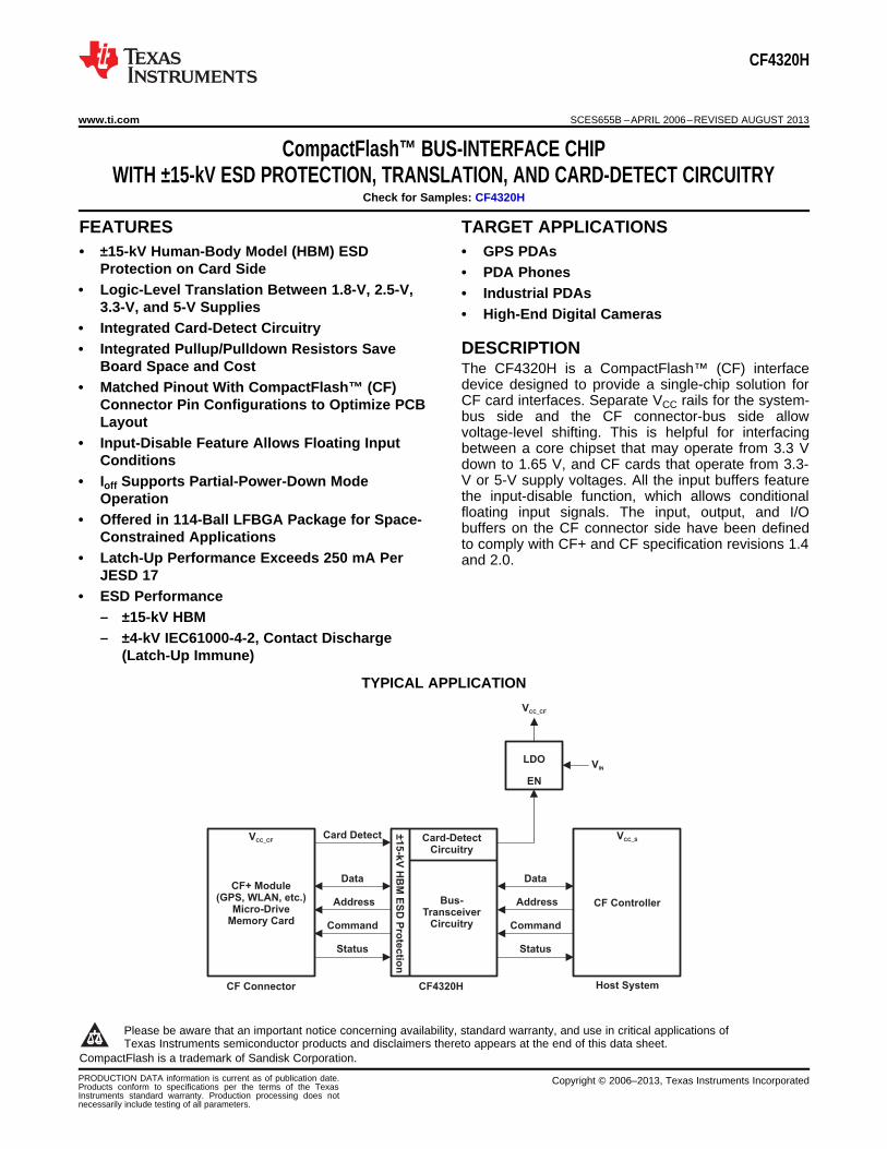
Board Space and Cost The CF4320H is a CompactFlash™ (CF) interfacedevice designed to provide a single-chip solution for• Matched Pinout With CompactFlash™ (CF)CF card interfaces. Separate VCC rails for the system-Connector Pin Configurations to Optimize PCBbus side and the CF connector-bus side allowLayoutvoltage-level shifting. This is helpful for interfacing
• Input-Disable Feature Allows Floating Input between a core chipset that may operate from 3.3 VConditions down to 1.65 V, and CF cards that operate from 3.3-
V or 5-V supply voltages. All the input buffers feature• Ioff Supports Partial-Power-Down Modethe input-disable function, which allows conditionalOperationfloating input signals. The input, output, and I/O• Offered in 114-Ball LFBGA Package for Space- buffers on the CF connector side have been definedConstrained Applications to comply with CF+ and CF specification revisions 1.4
• Latch-Up Performance Exceeds 250 mA Per and 2.0.JESD 17
• ESD Performance– ±15-kV HBM– ±4-kV IEC61000-4-2, Contact Discharge
(Latch-Up Immune)
TYPICAL APPLICATION
1
Please be aware that an important notice concerning availability, standard warranty, and use in critical applications ofTexas Instruments semiconductor products and disclaimers thereto appears at the end of this data sheet.
2CompactFlash is a trademark of Sandisk Corporation.PRODUCTION DATA information is current as of publication date. Copyright © 2006–2013, Texas Instruments IncorporatedProducts conform to specifications per the terms of the TexasInstruments standard warranty. Production processing does notnecessarily include testing of all parameters.

CF4320H
SCES655B –APRIL 2006–REVISED AUGUST 2013 www.ti.com
CARD-DETECT CIRCUITThe CF4320H has an integrated card-detect circuit that generates a LOW card-detect signal when a CF card isplugged into the socket. This circuit is supplied by a separate power-supply pin, VCC_SD, which operates from1.65 V to 5.5 V. The card-detect signal can be used to control a voltage regulator, which may power the CF slotand the CF side of the CF4320H. The inputs to this circuitry (CD1 and CD2) have internal pullup resistors to pullthem to a HIGH logic state if there is no card in the CF slot. VCC_SD is particularly helpful when the coreprocessor operates at a low VCC, but the regulator needs a higher control-signal voltage.
Table 1. CARD-DETECTSIGNALS
INPUTS OUTPUTSCDCD1 CD2
L L LL H HH L HH H H
BUS-TRANSCEIVER CIRCUIT
Command and Status BitsMost CF controllers are embedded in processors or microcontrollers and use GPIOs to send command signalsand receive status signals from the card to manage operation. The CF interface consists of eight control signalsand six status signals. The CF standard requires that each of these signals have a 100-kΩ pullup resistor. TheCF4320H includes an internal 100-kΩ pullup resistor on the input of each of these signals, which saves boardreal estate and lowers overall system cost
COMMAND LINE BUFFERS (1)
(BVD1, BVD2, INPACK, OE, IORD, IOWR,READY, REG, CE1, CE2, WAIT, WE, WP)
INPUTSOUTPUT
MASTER_EN BUF_EN INPUTL L H HL L L LL H X Z, Command line buffer inputs can float.H X X Z, low-power mode
(1) X = H or L
RESET (1)
INPUTS OUTPUTRESETMASTER_EN SRESET
L H HL L LH X Z, low-power mode
(1) X = H or L
Data BitsThe CF4320H has 16 data lines organized as two groups of 8 bits each. The ENL signal controls the lower 8 bits(D07–D00), while the ENH signal controls the upper 8 bits (D15–D08).
2 Submit Documentation Feedback Copyright © 2006–2013, Texas Instruments Incorporated
Product Folder Links: CF4320H

CF4320H
www.ti.com SCES655B –APRIL 2006–REVISED AUGUST 2013
LOWER 8-BIT DATA BUS TRANSCEIVERS (1)
(D07–D00, SD07–SD00)INPUTS
OPERATIONMASTER_EN ENL DIR (S/CF)
L L H SD data to D busL L L D data to SD busL H X Isolation. D07–D00 and SD07–SD00 inputs can float.H X X Isolation, low-power mode
(1) X = H or L
UPPER 8-BIT DATA BUS TRANSCEIVERS (1)
(D15–D08, SD15–SD08)INPUTS
OPERATIONMASTER_EN ENH DIR (S/CF)
L L H SD data to D busL L L D data to SD busL H X Isolation. D15–D08 and SD15–SD08 inputs can float.H X X Isolation, low-power mode
(1) X = H or L
Address BitsThe CF4320H has 11 unidirectional address bits flowing from the system to the CF card.
ADDRESS BUS BUFFERS (1)
INPUTS OUTPUTAMASTER_EN BUF_EN SA
L L H HL L L LL H X Z, SA inputs can float.H X X Z, low-power mode
(1) X = H or L
Copyright © 2006–2013, Texas Instruments Incorporated Submit Documentation Feedback 3
Product Folder Links: CF4320H

CF4320H
SCES655B –APRIL 2006–REVISED AUGUST 2013 www.ti.com
Direction Signal BitThe DIR(S/CF) input controls the data direction between the system bus and the CF card. The CF4320H hascircuitry to generate a DIR_OUT signal using the SOE and SIORD signals. DIR(S/CF) and DIR_OUT are placedadjacent to each other, which is convenient for connecting DIR(S/CF) and DIR_OUT, if DIR_OUT is used. Thissaves an additional signal from the system controller to control the data direction. When either SOE or SIORD islow, the data direction is from the CF card side to the system side (DIR_OUT = L).
DIR_OUT (1)
INPUTS OUTPUTDIR_OUTBUF_EN MASTER_EN SOE SIORD
L L L L LL L L H LL L H L LL L H H HH L X X LX H X X Z, low-power mode
(1) X = H or L
4 Submit Documentation Feedback Copyright © 2006–2013, Texas Instruments Incorporated
Product Folder Links: CF4320H

J
H
G
F
E
D
C
B
A
21 3 4 65
P
N
M
L
K
T
R
U
W
V
CF4320H
www.ti.com SCES655B –APRIL 2006–REVISED AUGUST 2013
BOARD-OPTIMIZED PIN CONFIGURATION
GKF OR ZKF PACKAGE(TOP VIEW)
TERMINAL ASSIGNMENTS1 2 3 4 5 6
A D12 D04 D03 SD14 SD12 SD11B D13 D05 D11 SD13 SD10 SD09C D14 D06 SD15 SINPACK SD08 SD07D D15 D07 VCC_CF VCC_S SD06 SD05E CE2 CE1 GND GND SD04 SD03F OE A10 VCC_CF VCC_S SD02 SD01G A09 IORD GND GND SD00 SCE1H A08 IOWR VCC_CF VCC_S ENL ENHJ A07 WE GND GND MASTER_EN BUF_ENK A06 READY A05 SCE2 SOE SIORDL A04 RESET GND GND SWE SIOWRM A03 WAIT VCC_CF VCC_S SREADY SRESETN A02 INPACK GND GND SWAIT SREGP A01 REG VCC_CF GND SBVD2 SBVD1R A00 BVD2 VCC_CF VCC_S SA10 SWPT D00 BVD1 VCC_SD DIR(S/CF) SA08 SA09U D01 D08 CD1 DIR_OUT SA06 SA07V D02 D09 CD2 SA00 SA04 SA05W WP D10 SCD SA01 SA02 SA03
Copyright © 2006–2013, Texas Instruments Incorporated Submit Documentation Feedback 5
Product Folder Links: CF4320H
CF4320H
SCES655B –APRIL 2006–REVISED AUGUST 2013 www.ti.com
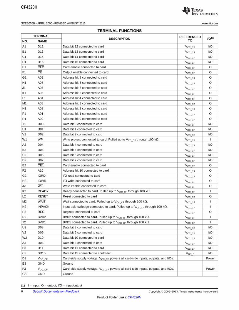
TERMINAL FUNCTIONSTERMINAL REFERENCEDDESCRIPTION I/O (1)
TONO. NAMEA1 D12 Data bit 12 connected to card VCC_CF I/OB1 D13 Data bit 13 connected to card VCC_CF I/OC1 D14 Data bit 14 connected to card VCC_CF I/OD1 D15 Data bit 15 connected to card VCC_CF I/OE1 CE2 Card enable connected to card VCC_CF OF1 OE Output enable connected to card VCC_CF OG1 A09 Address bit 9 connected to card VCC_CF OH1 A08 Address bit 8 connected to card VCC_CF OJ1 A07 Address bit 7 connected to card VCC_CF OK1 A06 Address bit 6 connected to card VCC_CF OL1 A04 Address bit 4 connected to card VCC_CF OM1 A03 Address bit 3 connected to card VCC_CF ON1 A02 Address bit 2 connected to card VCC_CF OP1 A01 Address bit 1 connected to card VCC_CF OR1 A00 Address bit 0 connected to card VCC_CF OT1 D00 Data bit 0 connected to card VCC_CF I/OU1 D01 Data bit 1 connected to card VCC_CF I/OV1 D02 Data bit 2 connected to card VCC_CF I/OW1 WP Write protect connected to card. Pulled up to VCC_CF through 100 kΩ. VCC_CF IA2 D04 Data bit 4 connected to card VCC_CF I/OB2 D05 Data bit 5 connected to card VCC_CF I/OC2 D06 Data bit 6 connected to card VCC_CF I/OD2 D07 Data bit 7 connected to card VCC_CF I/OE2 CE1 Card enable connected to card VCC_CF OF2 A10 Address bit 10 connected to card VCC_CF OG2 IORD I/O read connected to card VCC_CF OH2 IOWR I/O write connected to card VCC_CF OJ2 WE Write enable connected to card VCC_CF OK2 READY Ready connected to card. Pulled up to VCC_CF through 100 kΩ. VCC_CF IL2 RESET Reset connected to card VCC_CF OM2 WAIT Wait connected to card. Pulled up to VCC_CF through 100 kΩ. VCC_CF IN2 INPACK Input acknowledge connected to card. Pulled up to VCC_CF through 100 kΩ. VCC_CF IP2 REG Register connected to card VCC_CF OR2 BVD2 BVD2 connected to card. Pulled up to VCC_CF through 100 kΩ. VCC_CF IT2 BVD1 BVD1 connected to card. Pulled up to VCC_CF through 100 kΩ. VCC_CF IU2 D08 Data bit 8 connected to card VCC_CF I/OV2 D09 Data bit 9 connected to card VCC_CF I/OW2 D10 Data bit 10 connected to card VCC_CF I/OA3 D03 Data bit 3 connected to card VCC_CF I/OB3 D11 Data bit 11 connected to card VCC_CF I/OC3 SD15 Data bit 15 connected to controller VCC_S I/OD3 VCC_CF Card-side supply voltage. VCC_CF powers all card-side inputs, outputs, and I/Os. PowerE3 GND GroundF3 VCC_CF Card-side supply voltage. VCC_CF powers all card-side inputs, outputs, and I/Os. PowerG3 GND Ground
(1) I = input, O = output, I/O = input/output
6 Submit Documentation Feedback Copyright © 2006–2013, Texas Instruments Incorporated
Product Folder Links: CF4320H

CF4320H
www.ti.com SCES655B –APRIL 2006–REVISED AUGUST 2013
TERMINAL FUNCTIONS (continued)TERMINAL REFERENCEDDESCRIPTION I/O (1)
TONO. NAMEH3 VCC_CF Card-side supply voltage. VCC_CF powers all card-side inputs, outputs, and I/Os. PowerJ3 GND GroundK3 A05 Address bit 5 connected to card VCC_CF OL3 GND GroundM3 VCC_CF Card-side supply voltage. VCC_CF powers all card-side inputs, outputs, and I/Os. PowerN3 GND GroundP3 VCC_CF Card-side supply voltage. VCC_CF powers all card-side inputs, outputs, and I/Os. PowerR3 VCC_CF Card-side supply voltage. VCC_CF powers all card-side inputs, outputs, and I/Os. PowerT3 VCC_SD Card-detect supply voltage. VCC_SD powers the card-detect circuitry. PowerU3 CD1 Card detect connected to card. Pulled up to VCC_CF through 100 kΩ. VCC_SD IV3 CD2 Card detect connected to card. Pulled up to VCC_CF through 100 kΩ. VCC_SD IW3 SCD Card detect connected to controller VCC_SD OA4 SD14 Data bit 14 connected to controller VCC_S I/OB4 SD13 Data bit 13 connected to controller VCC_S I/OC4 SINPACK Input acknowledge connected to controller VCC_S I/O
Controller-side supply voltage. VCC_S powers all controller-side inputs, outputs,D4 VCC_S Powerand I/Os.E4 GND Ground
Controller-side supply voltage. VCC_S powers all controller-side inputs, outputs,F4 VCC_S Powerand I/Os.G4 GND Ground
Controller-side supply voltage. VCC_S powers all controller-side inputs, outputs,H4 VCC_S Powerand I/Os.J4 GND GroundK4 SCE2 Card enable connected to controller VCC_S IL4 GND Ground
Controller-side supply voltage. VCC_S powers all controller-side inputs, outputs,M4 VCC_S Powerand I/Os.N4 GND GroundP4 GND Ground
Controller-side supply voltage. VCC_S powers all controller-side inputs, outputs,R4 VCC_S Powerand I/Os.T4 DIR(S/CF) Direction controls flow of data from system to CF and vice-versa VCC_S IU4 DIR_OUT Data direction generated by CF4320H. Can be connected to DIR(S/CF). VCC_S OV4 SAO0 Address bit 0 connected to controller VCC_S IW4 SAO1 Address bit 1 connected to controller VCC_S IA5 SD12 Data bit 12 connected to controller VCC_S I/OB5 SD10 Data bit 10 connected to controller VCC_S I/OC5 SD08 Data bit 8 connected to controller VCC_S I/OD5 SD06 Data bit 6 connected to controller VCC_S I/OE5 SD04 Data bit 4 connected to controller VCC_S I/OF5 SD02 Data bit 2 connected to controller VCC_S I/OG5 SD00 Data bit 0 connected to controller VCC_S I/OH5 ENL Enable for data bits 0–7. Pulled up to VCC_S through 100 kΩ. VCC_S IJ5 MASTER_EN Enable for all transceivers and buffers except the card-detect circuitry VCC_S IK5 SOE Output enable connected to controller VCC_S IL5 SWE Write enable connected to controller VCC_S IM5 SREADY Ready connected to controller VCC_S O
Copyright © 2006–2013, Texas Instruments Incorporated Submit Documentation Feedback 7
Product Folder Links: CF4320H

CF4320H
SCES655B –APRIL 2006–REVISED AUGUST 2013 www.ti.com
TERMINAL FUNCTIONS (continued)TERMINAL REFERENCEDDESCRIPTION I/O (1)
TONO. NAMEN5 SWAIT Wait connected to controller VCC_S OP5 SBVD2 BVD2 connected to controller VCC_S OR5 SA10 Address bit 10 connected to controller VCC_S IT5 SA08 Address bit 8 connected to controller VCC_S IU5 SA06 Address bit 6 connected to controller VCC_S IV5 SA04 Address bit 4 connected to controller VCC_S IW5 SA02 Address bit 2 connected to controller VCC_S IA6 SD11 Data bit 11 connected to controller VCC_S I/OB6 SD09 Data bit 9 connected to controller VCC_S I/OC6 SD07 Data bit 7 connected to controller VCC_S I/OD6 SD05 Data bit 5 connected to controller VCC_S I/OE6 SD03 Data bit 3 connected to controller VCC_S I/OF6 SD01 Data bit 1 connected to controller VCC_S I/OG6 SCE1 Card enable connected to controller VCC_S IH6 ENH Enable for data bits 8–15. Pulled up to VCC_S through 100 kΩ. VCC_S IJ6 BUF_EN Enable for address and control/status lines. Pulled up to VCC_S through 100 kΩ. VCC_S IK6 SIORD I/O read connected to controller VCC_S IL6 SIOWR I/O write connected to controller VCC_S IM6 SRESET Reset connected to controller VCC_S IN6 SREG Register connected to controller VCC_S IP6 SBVD1 BVD1 connected to controller VCC_S OR6 SWP Write protect connected to controller VCC_S OT6 SA09 Address bit 9 connected to controller VCC_S IU6 SA07 Address bit 7 connected to controller VCC_S IV6 SA05 Address bit 5 connected to controller VCC_S IW6 SA03 Address bit 3 connected to controller VCC_S I
8 Submit Documentation Feedback Copyright © 2006–2013, Texas Instruments Incorporated
Product Folder Links: CF4320H

SD07−SD00D07−D00
SD15−SD08
8 8
A10−A00 SA10−SA00
SRESETRESET
11 11
7 7
6 6
2
DIR_OUT
D15−D088 8
SCD
CE1, CE2, IORD,IOWR, OE, REG, WE
BVD1, BVD2, INPACK,READY, WAIT, WP
CD1
CD2
DIR(S/CF)
ENL
MASTER_EN
ENH
BUF_EN
SCE1, SCE2, SIORD,SIOWR, SOE, SREG,SWE
SBVD1, SBVD2, SINPACK,SREADY, SWAIT, SWP
NOTE: R INT ≥ 100 kΩ
To 7 Other Channels
SIORD−INTSOE−INT
SIORD−INTSOE−INT
R INT
To 7 Other Channels
To 7 Other Channels To 7 Other Channels
T
R
A
N
S
L
A
T
I
O
N
VCC_SDVCC_SD
R INT
VCC_SD
R INT
VCC_SVCC_CF
VCC_S
VCC_S
R INT
R INT
VCC_S
R INT
VCC_CF
CF4320H
www.ti.com SCES655B –APRIL 2006–REVISED AUGUST 2013
LOGIC DIAGRAM
Copyright © 2006–2013, Texas Instruments Incorporated Submit Documentation Feedback 9
Product Folder Links: CF4320H

GND1
D032
D043
D054
D065
D076
CE17
A108
OE9
A0910
A0811
A0712
VCC13
A0614
A0515
A0416
A0317
A0218
A0119
A0020
D0021
D0122
D0223
WP24
CD225
CD126
D1127
D1228
D1329
D1430
D1531
CE232
VS133
IORD34
IOWR35
WE36
READY37
VCC38
CSEL 39
VS240
RESET41
WAIT 42
INPACK43
REG44
BVD2 45
BVD146
D0847
D09 48
D1049
GND50
J167155-CF CONNECTOR
SCD3W
D001T
D011U
D021V
D033A
D042A
D052B
D062C
D072D
D082U
D092V
D102W
D113B
D121A
D131B
D141C
D151D
RESET2L
A001R
A011P
A021N
A031M
A041L
A053K
A061K
A071J
A081H
A091G
A102F
CE12E
CE21E
IORD2G
IOWR2H
OE1F
REG2P
WE2J
BVD12T
BVD22R
INPACK2N
READY2K
WAIT2M
WP1W
CD23V
SD005G
SD016F
SD025F
SD036E
SD045E
SD056D
SD065D
SD076C
SD085C
SD096B
SD105B
SD116A
SD125A
SD134B
SD144A
SD153C
SRESET6M
SA004V
SA014W
SA025W
SA036W
SA04 5V
SA056V
SA065U
SA076U
SA085T
SA096T
SA10 5R
SCE16G
SCE24K
SIORD6K
SIOWR6L
SOE5K
SREG 6N
SWE5L
SBVD16P
SBVD25P
SINPACK4C
SREADY5M
SWAIT 5N
SWP6R
CD13U
EN_L5H
EN_H6H
MASTER_EN5J
BUF_EN6J
DIR(S/CF)4T
DIR_OUT4U
VCC_S4R
VCC_S4M
VCC_S4H
VCC_S4F
VCC_S4D
VCC_CF3R
VCC_CF3P
VCC_CF3M
VCC_CF3H
VCC_CF3F
VCC_CF3D
VCC_S3T
GND3E
GND3G
GND3J
GND3L
GND3N GND 4PGND
4NGND
4LGND
4GGND
4E
U1
CF4320H
DATA0DATA1DATA2DATA3DATA4DATA5DATA6DATA7DATA8DATA9DATA10DATA11DATA12DATA13DATA14DATA15RESETADD_0ADD_1ADD_2ADD_3ADD_4ADD_5ADD_6ADD_7ADD_8ADD_9ADD_10CE1CE2IORDIOWROEREGWEBVD1BVD2INPACKREADYWAIT
EN_LEN_H
MASTER_ENBUF_EN
VCC_S
GNDWP
U2
CF_PROCESSOR
6GND
IN5
VCC_CF
VCC_CF
VCC_SYS
CD1D03D11D04D12D05D13D06D14D07D15CE1CE2A10VS1OEIORDA09IOWRA08WEA07READY
A06CSELA05VS2A04RESETA03WAITA02INPACKA01REGA00BVD2D00BVD1D01D08D02D09WPD10CD2
D00D01D02D03D04D05D06D07D08D09D10D11D12D13D14D15RESETA00A01A02A03A04A05A06A07A08A09A10CE1CE2IORDIOWROEREGWEBVD1BVD2INPACKREADYWAITWP
C30.1 µF
OUTPG2
OUT
ENNC/FB1
IN3
7
4
8
4.7 µF
C2
3.3 KW
R1
0.1 µF
C1
VCC_CFTPS766xx
CF4320H
SCES655B –APRIL 2006–REVISED AUGUST 2013 www.ti.com
10 Submit Documentation Feedback Copyright © 2006–2013, Texas Instruments Incorporated
Product Folder Links: CF4320H

CF4320H
www.ti.com SCES655B –APRIL 2006–REVISED AUGUST 2013
Absolute Maximum Ratings (1)
over operating free-air temperature range (unless otherwise noted)MIN MAX UNIT
VCC_S –0.5 4.6Supply voltage range VVCC_CF –0.5 6.5VCC_SD
SD, SA (2) –0.5 4.6I/O ports
D, A –0.5 6.5SCE1, SCE2, SIORD, –0.5 4.6SIOWR, SOE, SREG, SWEVI Input voltage range VInput portsBVD1, BVD2, READY, –0.5 6.5INPACK, WAIT, WPDIR(S/CF), MASTER_EN,Control ports –0.5 4.6ENL, ENH
Voltage range applied to any output System port –0.5 4.6VO in the high-impedance or power-off V
CF port –0.5 6.5state (2)
System port –0.5 VCC_S + 0.5Voltage range applied to any outputVO Vin the high or low state (2) (3) CF port –0.5 VCC_CF + 0.5IIK Input clamp current VI < 0 –50 mAIOK Output clamp current VO < 0 –50 mAIO Continuous output current ±50 mA
Continuous current through each VCC_S, VCC_CF, VCC_SD, or GND ±100 mAθJA Package thermal impedance (4) 36 °C/WTstg Storage temperature range –65 150 °C
(1) Stresses beyond those listed under "absolute maximum ratings" may cause permanent damage to the device. These are stress ratingsonly, and functional operation of the device at these or any other conditions beyond those indicated under "recommended operatingconditions" is not implied. Exposure to absolute-maximum-rated conditions for extended periods may affect device reliability.
(2) The input and output negative-voltage ratings may be exceeded if the input and output current ratings are observed.(3) This value is limited to 6.5 V maximum.(4) The package thermal impedance is calculated in accordance with JESD 51-7.
Copyright © 2006–2013, Texas Instruments Incorporated Submit Documentation Feedback 11
Product Folder Links: CF4320H

CF4320H
SCES655B –APRIL 2006–REVISED AUGUST 2013 www.ti.com
Recommended Operating Conditions (1) (2) (3)
VCCI VCCO MIN MAX UNITVCC_SD Card-detect supply voltage 1.65 5.5 VVCC_S System-side supply voltage 1.65 VCC_CF VVCC_CF CF-side supply voltage 3 5.5 V
Card-detect inputsVIH High-level input voltage 1.65 V to 5.5 V VCC_SD × 0.65 V(CD1, CD2)Card-detect inputsVIL Low-level input voltage 1.65 V to 5.5 V VCC_SD × 0.35 V(CD1, CD2)
1.65 V to 1.95 V VCC_S × 0.65System portVIH High-level input voltage 1.95 V to 2.7 V 1.7 V(SD, SA, SRESET)
2.7 V to 3.6 V 21.65 V to 1.95 V VCC_S × 0.35
System portVIL Low-level input voltage 1.95 V to 2.7 V 0.7 V(SD, SA, SRESET)2.7 V to 3.6 V 0.8
1.65 V to 1.95 V VCC_S × 0.65Control inputsVIH High-level input voltage (DIR, MASTER_EN, 1.95 V to 2.7 V 1.7 V
ENL, ENH, BUF_EN) 2.7 V to 3.6 V 21.65 V to 1.95 V VCC_S × 0.35Control inputs
VIL Low-level input voltage (DIR, MASTER_EN, 1.95 V to 2.7 V 0.7 VENL, ENH, BUF_EN) 2.7 V to 3.6 V 0.8
3 V to 3.6 V 2VIH High-level input voltage CF port (D, A) V
4.5 V to 5.5 V VCC_CF × 0.73 V to 3.6 V 0.8
VIL Low-level input voltage CF port (D, A) V4.5 V to 5.5 V VCC_CF × 0.3
Card-detect output voltage 0 VCC_SD
VO System-side output voltage 0 VCC_S VCF-side output voltage 0 VCC_CF
1.65 V to 1.95 V –21.95 V to 2.7 V –4High-levelIOH Card detect mAoutput current 2.7 V to 3.6 V –84.5 V to 5.5 V –12
1.65 V to 1.95 V 21.95 V to 2.7 V 4Low-levelIOL Card detect mAoutput current 2.7 V to 3.6 V 84.5 V to 5.5 V 12
1.65 V to 1.95 V 2High-levelIOH System port 1.95 V to 2.7 V 6 mAoutput current
2.7 V to 3.6 V 121.65 V to 1.95 V 2
Low-levelIOL System port 1.95 V to 2.7 V 6 mAoutput current2.7 V to 3.6 V 123 V to 3.6 V 12High-levelIOH CF port mAoutput current 4.5 V to 5.5 V 163 V to 3.6 V 12Low-levelIOL CF port mAoutput current 4.5 V to 5.5 V 16
(1) VCCI is the VCC associated with the input port.(2) VCCO is the VCC associated with the output port.(3) All unused data inputs of the device must be held at VCCI or GND to ensure proper device operation. Refer to the TI application report,
Implications of Slow or Floating CMOS Inputs, literature number SCBA004.
12 Submit Documentation Feedback Copyright © 2006–2013, Texas Instruments Incorporated
Product Folder Links: CF4320H

CF4320H
www.ti.com SCES655B –APRIL 2006–REVISED AUGUST 2013
Recommended Operating Conditions(1) (2) (3) (continued)VCCI VCCO MIN MAX UNIT
1.65 V to 2.7 V >20Δt/Δv Input transition rise or fall rate 2.7 V to 3.6 V >20 ns/V
4.5 V to 5.5 V >20TA Operating free-air temperature –40 85 °C
Electrical Characteristicsover recommended operating free-air temperature range (CF card-detect logic) (unless otherwise noted)
TA = 25°C –40°C to 85°CPARAMETER TEST CONDITIONS VCC_SD UNIT
MIN TYP MAX MIN MAXIOH = –100 μA 1.65 V to 5.5 V VCC_SD – 0.1 VCC_SD – 0.2IOH = –2 mA 1.65 V 1.2 1.2IOH = –4 mA 2.3 V 2 2
VOH VI = VIH VIOH = –6 mA 2.7 V 2.3 2.3IOH = –8 mA 3 V 2.4 2.4IOH = –12 mA 4.5 V 3.8 3.8IOL = 100 μA 1.65 V to 5.5 V 0.1 0.2IOL = 2 mA 1.65 V 0.2 0.2IOL = 4 mA 2.3 V 0.2 0.2
VOL VI = VIL VIOL = 6 mA 2.7 V 0.3 0.3IOL = 8 mA 3 V 0.4 0.4IOL = 12 mA 4.5 V 0.5 0.5
VI = VCC_SD ±0.5 ±1II 1.65 V to 5.5 V μA
VI = 0 V –55 –60Ioff VI or VO = 0 to 5.5 V 0 V 55 60 μARINT CD1 = GND, CD2 = GND 1.65 V to 5.5 V 150 300 100 300 kΩ
CD1 and CD2 = VCC_SD, 0.5 1IO_SD = 0ICC_SD 5.5 V μACD1 or CD2 = GND,
CD2 or CD1 = VCC_SD, 10 10IO_SD = 0
CI CD1 or CD2 VI = VCC_SD or GND 5.5 V 9 pF
Copyright © 2006–2013, Texas Instruments Incorporated Submit Documentation Feedback 13
Product Folder Links: CF4320H

CF4320H
SCES655B –APRIL 2006–REVISED AUGUST 2013 www.ti.com
Electrical Characteristics (1) (2)
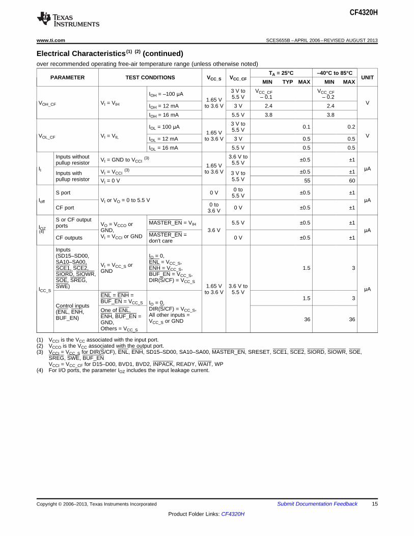
over recommended operating free-air temperature range (unless otherwise noted)TA = 25°C –40°C to 85°C
PARAMETER TEST CONDITIONS VCC_S VCC_CF UNITMIN TYP MAX MIN MAX
1.65 V 0.95 0.6 1.4SOE, SCE1,
2.3 V 1.32 0.9 1.8SCE2, SIORD,VT+ 3 V to 5.5 V VSIOWR, SWE, 2.7 V 1.49 1 2SREG
3 V 1.67 1.2 2.21.65 V 0.66 0.19 0.8
SOE, SCE1,2.3 V 0.87 0.39 1.15SCE2, SIORD,VT– 3 V to 5.5 V VSIOWR, SWE, 2.7 V 0.98 0.49 1.32
SREG3 V 1.08 0.59 1.5
1.65 V 0.31 0.1 0.7SOE, SCE1,
2.3 V 0.46 0.25 0.7SCE2, SIORD,ΔVT 3 V to 5.5 V VSIOWR, SWE, 2.7 V 0.52 0.3 0.9SREG
3 V 0.61 0.4 0.9BVD1, BVD2, 3 V 1.67 1.3 2.21.65 VVT+ READY, Vto 3.6 V 4.5 V 2.44 1.9 3.1INPACK, WAITBVD1, BVD2, 3 V 1.11 0.6 1.5READY, 1.65 VVT– VINPACK, WAIT, to 3.6 V 4.5 V 1.43 1 2WPBVD1, BVD2, 3 V 0.58 0.35 11.65 VΔVT READY, Vto 3.6 V 4.5 V 1.02 0.6 1.5INPACK, WAIT
1.65 V 1 0.6 1.4BUF_EN, ENH, 2.3 V 1.37 1.1 1.8
VT+ ENL, 3 V to 5.5 V V2.7 V 1.54 1.1 2MASTER_EN3 V 1.72 1.3 2.2
1.65 V 0.34 0.15 1BUF_EN, ENH, 2.3 V 0.63 0.15 1.2
VT– ENL, 3 V to 5.5 V V2.7 V 0.75 0.2 1.32MASTER_EN3 V 0.88 0.4 1.5
1.65 V 0.67 0.08 1.1BUF_EN, ENH, 2.3 V 0.76 0.2 1.2
ΔVT ENL, 3 V to 5.5 V V2.7 V 0.8 0.26 1.3MASTER_EN3 V 0.86 0.3 1.4
1.65 V VCC_S VCC_SIOH = –100 μA to 3.6 V – 0.1 – 0.2IOH = –2 mA 1.65 V 1.2 1.2
VOH_S VI = VIH 3 V to 5.5 V VIOH = –4 mA 2.3 V 2 2IOH = –6 mA 2.7 V 2.3 2.3IOH = –12 mA 3 V 2.4 2.4
1.65 VIOL = 100 μA 0.1 0.2to 3.6 VIOL = 2 mA 1.65 V 0.2 0.2
VOL_S VI = VIL 3 V to 5.5 V VIOL = 4 mA 2.3 V 0.2 0.2IOL = 6 mA 2.7 V 0.3 0.3IOL = 12 mA 3 V 0.5 0.5
(1) VCCI is the VCC associated with the input port.(2) VCCO is the VCC associated with the output port.
14 Submit Documentation Feedback Copyright © 2006–2013, Texas Instruments Incorporated
Product Folder Links: CF4320H
CF4320H
www.ti.com SCES655B –APRIL 2006–REVISED AUGUST 2013
Electrical Characteristics (1) (2) (continued)over recommended operating free-air temperature range (unless otherwise noted)
TA = 25°C –40°C to 85°CPARAMETER TEST CONDITIONS VCC_S VCC_CF UNIT
MIN TYP MAX MIN MAX3 V to VCC_CF VCC_CFIOH = –100 μA 5.5 V – 0.1 – 0.21.65 VVOH_CF VI = VIH VIOH = 12 mA to 3.6 V 3 V 2.4 2.4
IOH = 16 mA 5.5 V 3.8 3.83 V toIOL = 100 μA 0.1 0.25.5 V1.65 VVOL_CF VI = VIL VIOL = 12 mA to 3.6 V 3 V 0.5 0.5
IOL = 16 mA 5.5 V 0.5 0.5Inputs without 3.6 V toVI = GND to VCCI
(3) ±0.5 ±1pullup resistor 5.5 V1.65 VII μAVI = VCCI(3) to 3.6 V ±0.5 ±1Inputs with 3 V to
pullup resistor 5.5 VVI = 0 V 55 600 toS port 0 V ±0.5 ±15.5 V
Ioff VI or VO = 0 to 5.5 V μA0 toCF port 0 V ±0.5 ±13.6 V
S or CF output MASTER_EN = VIH 5.5 V ±0.5 ±1VO = VCCO orportsIOZ GND, 3.6 V μA(4) MASTER_EN =VI = VCCI or GNDCF outputs 0 V ±0.5 ±1don't careInputs(SD15–SD00, IO = 0,SA10–SA00, ENL = VCC_S,VI = VCC_S orSCE1, SCE2, ENH = VCC_S, 1.5 3GNDSIORD, SIOWR, BUF_EN = VCC_S,SOE, SREG, DIR(S/CF) = VCC_S
1.65 V 3.6 V toSWE)ICC_S μAto 3.6 V 5.5 VENL = ENH = 1.5 3BUF_EN = VCC_S IO = 0,Control inputs DIR(S/CF) = VCC_S,One of ENL,(ENL, ENH, All other inputs =ENH, BUF_EN =BUF_EN) 36 36VCC_S or GNDGND,Others = VCC_S
(1) VCCI is the VCC associated with the input port.(2) VCCO is the VCC associated with the output port.(3) VCCI = VCC_S for DIR(S/CF), ENL, ENH, SD15–SD00, SA10–SA00, MASTER_EN, SRESET, SCE1, SCE2, SIORD, SIOWR, SOE,
SREG, SWE, BUF_ENVCCI = VCC_CF for D15–D00, BVD1, BVD2, INPACK, READY, WAIT, WP
(4) For I/O ports, the parameter IOZ includes the input leakage current.
Copyright © 2006–2013, Texas Instruments Incorporated Submit Documentation Feedback 15
Product Folder Links: CF4320H

CF4320H
SCES655B –APRIL 2006–REVISED AUGUST 2013 www.ti.com
Electrical Characteristics (continued)over recommended operating free-air temperature range (unless otherwise noted)
TA = 25°C –40°C to 85°CPARAMETER TEST CONDITIONS VCC_S VCC_CF UNIT
MIN TYP MAX MIN MAXIO = 0,DIR(S/CF) = GND,Input VI = VCC_CF BVD1, BVD2, INPACK, 1.5 3(D15–D00) or GND READY, WAIT, WP =VCC_CF
Inputs BVD1 = BVD2 = IO = 0,(BVD1, BVD2, INPACK = DIR(S/CF) = GND, 1.65 V 3 V toICC_CF INPACK, 1.5 3 μAREADY WAIT = D15–D00 = VCC_CF or to 3.6 V 5.5 VREADY, WAIT, WP = VCC_CF GNDWP)One of BVD1, IO = 0,DVD2, INPACK, DIR(S/CF) = GND,READY, WAIT, 60 60D15–D00 = VCC_CF orWP = GND, All GNDothers = VCC_CF
1.65 V 3 V toRINT 150 300 300 kΩto 3.6 V 5.5 VControl inputs 3SAxx, SOE,SCE1, SCE2, 3SIORD, SIOWR,
CI SREG, SWE VI = 3.3 V or GND 3.3 V 3.3 V pFAxx, BVD1,BVD2, READY, 9INPACK, WAIT,WPS I/O ports 7
Cio VO = 3.3 V or GND 3.3 V 3.3 V pFCF I/O ports 12
16 Submit Documentation Feedback Copyright © 2006–2013, Texas Instruments Incorporated
Product Folder Links: CF4320H

CF4320H
www.ti.com SCES655B –APRIL 2006–REVISED AUGUST 2013
Switching Characteristicsover recommended operating free-air temperature range (CD1, CD2) (see Figure 1)
TA = 25°C –40°C to 85°CFROM TOPARAMETER VCC_SD UNIT(INPUT) (OUTPUT) MIN TYP MAX MIN MAX1.8 V ± 0.15 V 3.1 7.1 13.5 1.8 15.52.5 V ± 0.2 V 2.7 4.6 7.1 1.6 9.1
tpd CD1 or CD2 SCD 2.7 V 2.4 4 5.7 1.6 9.1 ns3.3 V ± 0.3 V 2 3.4 5.1 1.2 6.85 V ± 0.5 V 1.7 2.6 3.6 1 5.5
Switching Characteristicsover recommended operating free-air temperature range (BVD1, BVD2, INPACK, READY, WAIT, WP) (see Figure 1)
–40°C toTA = 25°CFROM TO TEST 85°CPARAMETER VCC_S VCC_CF UNIT(INPUT) (OUTPUT) CONDITIONSMIN TYP MAX MIN MAX
3.3 V ± 0.3 V 3.1 6 10.2 2.4 12.91.8 V ± 0.15 V
5 V ± 0.5 V 2.9 5.6 9.6 2.2 13.93.3 V ± 0.3 V 2.7 4.6 6.5 1.9 10MASTER_EN =tpd CF input S output 2.5 V ± 0.2 V nsBUF_EN = VIL 5 V ± 0.5 V 2.5 4.2 5.8 1.7 8.63.3 V ± 0.3 V 2.5 4 5.6 1.6 8.8
3.3 V ± 0.3 V5 V ± 0.5 V 2.3 3.6 4.9 1.5 7
3.3 V ± 0.3 V 11.1 18.9 30.7 9.2 35.51.8 V ± 0.15 V
5 V ± 0.5 V 11.1 19.3 30.9 8 35.63.3 V ± 0.3 V 9.9 12.9 17.4 6.9 22.6
ten MASTER_EN S output BUF_EN = VIL 2.5 V ± 0.2 V ns5 V ± 0.5 V 9.9 13.1 17.4 7 22.6
3.3 V ± 0.3 V 9.5 11.2 13.4 6.3 18.33.3 V ± 0.3 V
5 V ± 0.5 V 9.5 11.3 13.5 6.3 18.23.3 V ± 0.3 V 6.8 13.7 23.9 6 25.1
1.8 V ± 0.15 V5 V ± 0.5 V 6.1 13.4 22 5.4 23.3
3.3 V ± 0.3 V 4.9 8.6 13.3 4 14.5tdis MASTER_EN S output BUF_EN = VIL 2.5 V ± 0.2 V ns
5 V ± 0.5 V 4.6 8.5 13.6 3.9 14.53.3 V ± 0.3 V 5 8.1 12.2 4.2 13.2
3.3 V ± 0.3 V5 V ± 0.5 V 4.5 8 12.2 3.6 18.2
3.3 V ± 0.3 V 8.7 17.7 33.2 7.6 35.51.8 V ± 0.15 V
5 V ± 0.5 V 10.7 18..3 29.3 8.7 35.63.3 V ± 0.3 V 9.6 12.4 16.6 6.6 22.6MASTER_EN =ten BUF_EN S output 2.5 V ± 0.2 V nsVIL 5 V ± 0.5 V 9.6 12.6 16.7 6.6 22.63.3 V ± 0.3 V 9.2 10.9 13 6.1 18.3
3.3 V ± 0.3 V5 V ± 0.5 V 9.2 10.9 13 6.1 18.2
3.3 V ± 0.3 V 6.9 12.9 22.3 5.9 24.21.8 V ± 0.15 V
5 V ± 0.5 V 5.4 12.4 20.5 4.8 22.83.3 V ± 0.3 V 4.4 8 12.7 3.6 14.5MASTER_EN =tdis BUF_EN S output 2.5 V ± 0.2 V nsVIL 5 V ± 0.5 V 4.2 7.9 12.8 3.6 14.23.3 V ± 0.3 V 4.6 7.7 11.7 3.8 12.3
3.3 V ± 0.3 V5 V ± 0.5 V 4.1 7.6 11.7 3.3 12.4
Copyright © 2006–2013, Texas Instruments Incorporated Submit Documentation Feedback 17
Product Folder Links: CF4320H

CF4320H
SCES655B –APRIL 2006–REVISED AUGUST 2013 www.ti.com
Switching Characteristicsover recommended operating free-air temperature range (data bus I/Os) (see Figure 1)
–40°C toTA = 25°CFROM TO TEST 85°CPARAMETER VCC_S VCC_CF UNIT(INPUT) (OUTPUT) CONDITIONSMIN TYP MAX MIN MAX
3.3 V ± 0.3 V 4.2 7.2 11.8 3 13.71.8 V ±0.15 V 5 V ± 0.5 V 3.7 6.4 10.7 2.7 13.9
3.3 V ± 0.3 V 3.8 5.7 8 2.4 102.5 V ±D SD 0.2 V 5 V ± 0.5 V 3.3 4.9 6.8 2.1 12.43.3 V ± 0.3 V 3.5 5.1 6.9 2.2 8.83.3 V ±
0.3 V 5 V ± 0.5 V 3 4.3 5.7 1.8 7MASTER_EN =tpd nsENL = ENH = VIL 3.3 V ± 0.3 V 3.4 5.7 9.8 2.6 11.11.8 V ±0.15 V 5 V ± 0.5 V 3.1 5.4 9.6 2.4 9.6
3.3 V ± 0.3 V 2.8 4.3 6.2 1.9 8.22.5 V ±SD D 0.2 V 5 V ± 0.5 V 2.6 3.8 5.4 1.7 73.3 V ± 0.3 V 2.5 3.7 5.2 1.5 7.23.3 V ±
0.3 V 5 V ± 0.5 V 2.2 3.3 4.5 1.4 63.3 V ± 0.3 V 13.7 18.2 24.4 9.4 27.91.8 V ±
0.15 V 5.5 V ± 0.5 V 13.7 17.9 29.9 8 313.3 V ± 0.3 V 12.3 15.1 18.8 7.9 232.5 V ±D 0.2 V 5.5 V ± 0.5 V 12.3 14.8 17.6 8 21.83.3 V ± 0.3 V 11.6 14 17.1 7.3 21.43.3 V ±
0.3 V 5.5 V ± 0.5 V 11.6 13.7 15.9 7.4 20.3ten MASTER_EN ENL = ENH = VIL ns
3.3 V ± 0.3 V 11.6 19.6 31.8 9.4 36.31.8 V ±0.15 V 5.5 V ± 0.5 V 11.7 20.1 32 9.5 36.2
3.3 V ± 0.3 V 10.3 13.4 18 7.2 22.62.5 V ±SD 0.2 V 5.5 V ± 0.5 V 10.3 13.6 18.1 7.1 22.63.3 V ± 0.3 V 9.8 11.6 14 6.4 18.33.3 V ±
0.3 V 5.5 V ± 0.5 V 9.8 11.7 14 6.4 18.23.3 V ± 0.3 V 8.6 12.8 18.1 7.3 20.21.8 V ±
0.15 V 5.5 V ± 0.5 V 7.6 11.5 16.4 6.3 17.83.3 V ± 0.3 V 7.8 10.8 14.7 6.4 16.42.5 V ±D 0.2 V 5.5 V ± 0.5 V 6.7 9.4 12.6 5.4 13.83.3 V ± 0.3 V 7.2 9.9 13.4 5.9 153.3 V ±
0.3 V 5.5 V ± 0.5 V 6.1 8.6 11.4 4.8 12.5tdis MASTER_EN ENL = ENH = VIL ns
3.3 V ± 0.3 V 6.9 12.9 21.7 6 24.21.8 V ±0.15 V 5.5 V ± 0.5 V 6.1 12.6 20.8 5.3 22.8
3.3 V ± 0.3 V 4.9 7.9 11.8 4.1 14.52.5 V ±SD 0.2 V 5.5 V ± 0.5 V 4.7 7.8 11.7 3.9 14.23.3 V ± 0.3 V 5 7.1 9.8 4 123.3 V ±
0.3 V 5.5 V ± 0.5 V 4.7 7 9.8 3.8 18.2
18 Submit Documentation Feedback Copyright © 2006–2013, Texas Instruments Incorporated
Product Folder Links: CF4320H

CF4320H
www.ti.com SCES655B –APRIL 2006–REVISED AUGUST 2013
Switching Characteristics (continued)over recommended operating free-air temperature range (data bus I/Os) (see Figure 1)
–40°C toTA = 25°CFROM TO TEST 85°CPARAMETER VCC_S VCC_CF UNIT(INPUT) (OUTPUT) CONDITIONSMIN TYP MAX MIN MAX
3.3 V ± 0.3 V 9.4 17.6 23.4 8.3 27.21.8 V ±0.15 V 5.5 V ± 0.5 V 13.5 17.4 22.6 7.7 27.8
3.3 V ± 0.3 V 12.3 15 18.5 7.9 22.82.5 V ±D 0.2 V 5.5 V ± 0.5 V 12.3 14.7 17.4 8 21.63.3 V ± 0.3 V 11.7 14.1 17 7.3 21.43.3 V ±
0.3 V 5.5 V ± 0.5 V 11.6 13.7 16 7.4 20.3ten ENL or ENH MASTER_EN = VIL ns
3.3 V ± 0.3 V 9.5 18.7 30.5 9.1 35.51.8 V ±0.15 V 5.5 V ± 0.5 V 9.6 19.1 30.5 9.1 35.6
3.3 V ± 0.3 V 10 13 17.4 6.8 22.62.5 V ±SD 0.2 V 5.5 V ± 0.5 V 10 13.2 17.4 6.8 22.63.3 V ± 0.3 V 9.6 11.3 13.6 6.2 18.33.3 V ±
0.3 V 5.5 V ± 0.5 V 9.6 11.4 13.6 6.3 18.23.3 V ± 0.3 V 8.5 12.1 16.8 7.2 20.21.8 V ±
0.15 V 5.5 V ± 0.5 V 7.7 10.8 15 6.3 16.63.3 V ± 0.3 V 7.6 10.4 13.8 6.2 16.42.5 V ±D 0.2 V 5.5 V ± 0.5 V 6.9 9.1 11.9 5.4 13.13.3 V ± 0.3 V 7.3 9.7 12.9 5.9 153.3 V ±
0.3 V 5.5 V ± 0.5 V 6.5 8.4 11 5.2 12tdis ENL or ENH MASTER_EN = VIL ns
3.3 V ± 0.3 V 6.5 12 20 5.7 24.21.8 V ±0.15 V 5.5 V ± 0.5 V 5.7 11.8 19 5 22.8
3.3 V ± 0.3 V 4.6 7.4 11.1 3.8 14.52.5 V ±SD 0.2 V 5.5 V ± 0.5 V 4.4 7.3 11.1 3.7 14.23.3 V ± 0.3 V 4.9 6.8 9.3 4 123.3 V ±
0.3 V 5.5 V ± 0.5 V 4.3 6.7 9.2 3.5 18.2
Copyright © 2006–2013, Texas Instruments Incorporated Submit Documentation Feedback 19
Product Folder Links: CF4320H

CF4320H
SCES655B –APRIL 2006–REVISED AUGUST 2013 www.ti.com
Switching Characteristicsover recommended operating free-air temperature range (SA10–SA00, SCE1, SCE2, SIORD, SIOWR, SOE, SREG, SWE)(see Figure 1)
–40°C toTA = 25°CFROM TO TEST 85°CPARAMETER VCC_S VCC_CF UNIT(INPUT) (OUTPUT) CONDITIONSMIN TYP MAX MIN MAX
3.3 V ± 0.3 V 3.4 6.1 9.8 2.5 10.41.8 V ±0.15 V 5 V ± 0.5 V 3 5.8 9.7 2.4 10.2
MASTER_EN 3.3 V ± 0.3 V 2.6 4.5 6.7 1.8 8.4CF output 2.5 V ±= BUF_EN =(control) 0.2 V 5 V ± 0.5 V 2.4 4.1 6 1.7 6.8VIL3.3 V ± 0.3 V 2.2 3.9 5.8 1.4 73.3 V ±
0.3 V 5 V ± 0.5 V 2 3.5 5 1.3 5.8tpd S input ns
3.3 V ± 0.3 V 3.4 5.7 8.7 2.8 10.31.8 V ±0.15 V 5 V ± 0.5 V 3.3 5.4 8.2 2.8 9.7
MASTER_EN 3.3 V ± 0.3 V 2.9 4.3 6.2 1.9 8.4CF output 2.5 V ±= BUF_EN =(A pins) 0.2 V 5 V ± 0.5 V 2.7 3.9 5.4 1.9 6.8VIL3.3 V ± 0.3 V 2.6 3.7 5.2 1.7 7
3.3 V ± 0.3 V5 V ± 0.5 V 2.3 3.3 4.4 1.5 5.8
3.3 V ± 0.3 V 10.8 17.9 24.8 7.9 29.71.8 V ± 0.15 V
5 V ± 0.5 V 10.8 17.5 26.2 8.1 30.23.3 V ± 0.3 V 9.4 14.2 19.4 6.4 23.3CF outputten MASTER_EN BUF_EN = VIL 2.5 V ± 0.2 V ns(control) 5 V ± 0.5 V 9.4 14.1 19.3 6.6 23.13.3 V ± 0.3 V 8.7 13.1 17.8 5.8 21.4
3.3 V ± 0.3 V5 V ± 0.5 V 8.7 13 17.5 6 21.2
3.3 V ± 0.3 V 7.3 13.8 22.5 6.2 25.81.8 V ± 0.15 V
5 V ± 0.5 V 6.8 12.1 19.7 5.9 26.33.3 V ± 0.3 V 6.1 11.8 19.2 4.9 20.2CF outputtdis MASTER_EN BUF_EN = VIL 2.5 V ± 0.2 V ns(control) 5 V ± 0.5 V 5.9 10 16.3 4.6 19.83.3 V ± 0.3 V 5.6 11 18.3 4.6 19.1
3.3 V ± 0.3 V5 V ± 0.5 V 5.4 9.2 15.5 3.9 18
3.3 V ± 0.3 V 12.9 17.5 23.7 7.7 29.71.8 V ± 0.15 V
5 V ± 0.5 V 13.3 17.8 24.4 9.4 30.23.3 V ± 0.3 V 11.7 14.4 17.9 7.5 23.3CF output MASTER_ENten BUF_EN 2.5 V ± 0.2 V ns(A pins) = VIL 5 V ± 0.5 V 11.8 14.3 17.1 7.7 23.13.3 V ± 0.3 V 11 13.3 16.2 6.9 21.4
3.3 V ± 0.3 V5 V ± 0.5 V 11.1 13.2 15.3 6.5 21.2
3.3 V ± 0.3 V 8.9 13.6 19.7 7.5 25.81.8 V ± 0.15 V
5 V ± 0.5 V 7.6 11.8 17.1 6.6 26.33.3 V ± 0.3 V 8 11.6 16 6.6 20.1CF output MASTER_ENtdis BUF_EN 2.5 V ± 0.2 V ns(A pins) = VIL 5 V ± 0.5 V 6.7 9.7 13.2 5 19.83.3 V ± 0.3 V 7.7 10.6 14.7 6 18.2
3.3 V ± 0.3 V5 V ± 0.5 V 6.1 8.9 11.9 4.9 18
3.3 V ± 0.3 V 12.3 16.4 21.9 7.7 27.21.8 V ± 0.15 V
5 V ± 0.5 V 12.6 16.7 22.6 8.6 29.13.3 V ± 0.3 V 11.2 13.8 17 7.1 21.7CF output MASTER_ENten BUF_EN 2.5 V ± 0.2 V ns(A pins) = VIL 5 V ± 0.5 V 11.4 13.7 16.3 7.3 21.53.3 V ± 0.3 V 10.7 12.9 15.6 6.7 19.5
3.3 V ± 0.3 V5 V ± 0.5 V 10.8 12.8 14.8 6.5 19.6
20 Submit Documentation Feedback Copyright © 2006–2013, Texas Instruments Incorporated
Product Folder Links: CF4320H

CF4320H
www.ti.com SCES655B –APRIL 2006–REVISED AUGUST 2013
Switching Characteristics (continued)over recommended operating free-air temperature range (SA10–SA00, SCE1, SCE2, SIORD, SIOWR, SOE, SREG, SWE)(see Figure 1)
–40°C toTA = 25°CFROM TO TEST 85°CPARAMETER VCC_S VCC_CF UNIT(INPUT) (OUTPUT) CONDITIONSMIN TYP MAX MIN MAX
3.3 V ± 0.3 V 8.4 13.9 21.2 7.2 23.21.8 V ± 0.15 V
5 V ± 0.5 V 7.6 12.3 18.5 6.6 23.73.3 V ± 0.3 V 7.7 12.3 18.2 6.4 19.8CF output MASTER_ENtdis BUF_EN 2.5 V ± 0.2 V ns(A pins) = VIL 5 V ± 0.5 V 6.7 10.6 15.3 5 18.43.3 V ± 0.3 V 7.2 11.5 16.4 5.9 18
3.3 V ± 0.3 V5 V ± 0.5 V 6.4 10 14.3 4.9 17
3.3 V ± 0.3 V 12.5 16.6 22.3 8.7 27.21.8 V ± 0.15 V
5 V ± 0.5 V 12.8 17 23.1 8.8 29.13.3 V ± 0.3 V 11.4 14.1 17.5 7.3 21.7MASTER_ENten BUF_EN CF output 2.5 V ± 0.2 V ns= VIL 5 V ± 0.5 V 11.6 14 16.9 7.4 21.53.3 V ± 0.3 V 10.9 13.2 16 6.8 20
3.3 V ± 0.3 V5 V ± 0.5 V 11 13.1 15.3 6.5 19.6
3.3 V ± 0.3 V 8.6 13.9 21.5 7.4 23.21.8 V ± 0.15 V
5 V ± 0.5 V 7.7 12.1 19.8 6.6 23.73.3 V ± 0.3 V 7.9 12.3 18.5 6.5 19.8MASTER_ENtdis BUF_EN CF output 2.5 V ± 0.2 V ns= VIL 5 V ± 0.5 V 6.6 10.4 17.1 5 18.43.3 V ± 0.3 V 7.4 11.7 17.5 6.1 18.9
3.3 V ± 0.3 V5 V ± 0.5 V 6.1 9.7 16.2 4.9 17
3.3 V ± 0.3 V 6.1 14.2 29.6 4.9 32.81.8 V ± 0.15 V
5 V ± 0.5 V 6 14.2 30 4.9 33.23.3 V ± 0.3 V 4.8 8.8 15.4 3.4 19.3
ten MASTER_EN DIR_OUT BUF_EN = VIL 2.5 V ± 0.2 V ns5 V ± 0.5 V 4.8 8.8 15.5 3.4 19.3
3.3 V ± 0.3 V 4.2 6.9 11.1 2.7 14.43.3 V ± 0.3 V
5 V ± 0.5 V 4.2 6.9 11.1 2.6 14.43.3 V ± 0.3 V 5.4 10 16.6 4.2 32.6
1.8 V ± 0.15 V5 V ± 0.5 V 5.4 9.9 16.1 4.8 32.6
3.3 V ± 0.3 V 3.9 6.5 10.5 1.5 19.3tdis MASTER_EN DIR_OUT BUF_EN = VIL 2.5 V ± 0.2 V ns
5 V ± 0.5 V 3.9 6.6 10.4 1.7 19.33.3 V ± 0.3 V 4.4 6.7 10.3 1.4 14.4
3.3 V ± 0.3 V5 V ± 0.5 V 4.3 6.7 10.1 1.5 14.4
3.3 V ± 0.3 V 5 9.3 15.7 4 17.91.8 V ± 0.15 V
5 V ± 0.5 V 5 9.3 15.7 4 17.93.3 V ± 0.3 V 3.9 6 8.5 2.8 11SIORD ortpd DIR_OUT BUF_EN = VIL 2.5 V ± 0.2 V nsSOE 5 V ± 0.5 V 3.9 6 8.5 2.8 113.3 V ± 0.3 V 3.3 4.7 6.2 2.2 8.2
3.3 V ± 0.3 V5 V ± 0.5 V 3.3 4.7 6.2 2.2 8.2
3.3 V ± 0.3 V 8.9 19.5 35.9 7.1 39.21.8 V ± 0.15 V
5 V ± 0.5 V 8.9 19.5 35.8 7 39.33.3 V ± 0.3 V 6.8 11.9 19.1 5 22.8
tpd BUF_EN DIR_OUT BUF_EN = VIL 2.5 V ± 0.2 V ns5 V ± 0.5 V 6.8 11.9 19.2 4.9 22.8
3.3 V ± 0.3 V 5.8 9 13.3 4 15.83.3 V ± 0.3 V
5 V ± 0.5 V 5.8 9 13.3 3.9 15.9
Copyright © 2006–2013, Texas Instruments Incorporated Submit Documentation Feedback 21
Product Folder Links: CF4320H

CF4320H
SCES655B –APRIL 2006–REVISED AUGUST 2013 www.ti.com
Operating CharacteristicsVCCS and VCC_CF = 3.3 V, TA = 25°C
PARAMETER TEST CONDITIONS TYP UNITOutputs 1.93enabledSystem-port input,
CF-port output Outputs 0.04disabledPower dissipation capacitanceCpdS CL = 0, f = 10 MHz pFper transceiver Outputs 14.35enabledCF-port input,system-port output Outputs 0.04disabled
Outputs 22.85enabledSystem-port input,CF-port output Outputs 0.04disabledPower dissipation capacitanceCpdCF CL = 0, f = 10 MHz pFper transceiver Outputs 4.66enabledCF-port input,system-port output Outputs 3.65disabled
22 Submit Documentation Feedback Copyright © 2006–2013, Texas Instruments Incorporated
Product Folder Links: CF4320H

VM
VM
VMVM
VMVM
VMVM
VOH
VOL
thtsu
From OutputUnder Test
CL(see Note A)
LOAD CIRCUIT
S1 Open
GND
RL
RL
OutputControl
(low-levelenabling)
OutputWaveform 1S1 at VLOAD(see Note B)
OutputWaveform 2
S1 at GND(see Note B)
tPZL
tPZH
tPLZ
tPHZ
0 V
VOL + V∆
VOH − V∆
0 V
VI
0 V
0 V
tw
VIVI
VOLTAGE WAVEFORMSSETUP AND HOLD TIMES
VOLTAGE WAVEFORMSPULSE DURATION
VOLTAGE WAVEFORMSENABLE AND DISABLE TIMES
TimingInput
DataInput
Input
tpdtPLZ/tPZLtPHZ/tPZH
OpenVLOADGND
TEST S1
NOTES: A. CL includes probe and jig capacitance.B. Waveform 1 is for an output with internal conditions such that the output is low, except when disabled by the output control.
Waveform 2 is for an output with internal conditions such that the output is high, except when disabled by the output control.C. All input pulses are supplied by generators having the following characteristics: PRR ≤ 10 MHz, ZO = 50 Ω.D. The outputs are measured one at a time, with one transition per measurement.E. tPLZ and tPHZ are the same as tdis.F. tPZL and tPZH are the same as ten.G. tPLH and tPHL are the same as tpd.H. All parameters and waveforms are not applicable to all devices.
0 V
VI
VM
tPHL
VM VM
VI
0 V
VOH
VOL
Input
Output
VOLTAGE WAVEFORMSPROPAGATION DELAY TIMES
VM VM
tPLH
VLOAD
VLOAD/2
1.8 V ± 0.15 V2.5 ± 0.2 V
2.7 V3.3 V ± 0.3 V5.5 V ± 0.5 V
2 kΩ2 kΩ2 kΩ2 kΩ2 kΩ
VCC RL
2 × VCC2 × VCC
6 V6 V6 V
VLOAD CL
15 pF15 pF15 pF15 pF15 pF
0.15 V0.15 V0.3 V0.3 V0.5 V
V∆
VCCVCC2.7 V2.7 V2.7 V
VI
VCC/2VCC/21.5 V1.5 V1.5 V
VMtr/tf
≤2 ns≤2 ns
≤2.5 ns≤2.5 ns≤2.5 ns
INPUT
CF4320H
www.ti.com SCES655B –APRIL 2006–REVISED AUGUST 2013
PARAMETER MEASUREMENT INFORMATION
Figure 1. Load Circuit and Voltage Waveforms
Copyright © 2006–2013, Texas Instruments Incorporated Submit Documentation Feedback 23
Product Folder Links: CF4320H

CF4320H
SCES655B –APRIL 2006–REVISED AUGUST 2013 www.ti.com
REVISION HISTORY
Changes from Revision A (August 2006) to Revision B Page
• Removed Ordering Information table. ................................................................................................................................... 2
24 Submit Documentation Feedback Copyright © 2006–2013, Texas Instruments Incorporated
Product Folder Links: CF4320H

PACKAGE OPTION ADDENDUM
www.ti.com 31-Aug-2013
Addendum-Page 1
PACKAGING INFORMATION
Orderable Device Status(1)
Package Type PackageDrawing
Pins PackageQty
Eco Plan(2)
Lead/Ball Finish MSL Peak Temp(3)
Op Temp (°C) Device Marking(4/5)
Samples
CF4320HZKFR ACTIVE LFBGA ZKF 114 1000 Green (RoHS& no Sb/Br)
SNAGCU Level-3-260C-168 HR -40 to 85 CF4320
(1) The marketing status values are defined as follows:ACTIVE: Product device recommended for new designs.LIFEBUY: TI has announced that the device will be discontinued, and a lifetime-buy period is in effect.NRND: Not recommended for new designs. Device is in production to support existing customers, but TI does not recommend using this part in a new design.PREVIEW: Device has been announced but is not in production. Samples may or may not be available.OBSOLETE: TI has discontinued the production of the device.
(2) Eco Plan - The planned eco-friendly classification: Pb-Free (RoHS), Pb-Free (RoHS Exempt), or Green (RoHS & no Sb/Br) - please check http://www.ti.com/productcontent for the latest availabilityinformation and additional product content details.TBD: The Pb-Free/Green conversion plan has not been defined.Pb-Free (RoHS): TI's terms "Lead-Free" or "Pb-Free" mean semiconductor products that are compatible with the current RoHS requirements for all 6 substances, including the requirement thatlead not exceed 0.1% by weight in homogeneous materials. Where designed to be soldered at high temperatures, TI Pb-Free products are suitable for use in specified lead-free processes.Pb-Free (RoHS Exempt): This component has a RoHS exemption for either 1) lead-based flip-chip solder bumps used between the die and package, or 2) lead-based die adhesive used betweenthe die and leadframe. The component is otherwise considered Pb-Free (RoHS compatible) as defined above.Green (RoHS & no Sb/Br): TI defines "Green" to mean Pb-Free (RoHS compatible), and free of Bromine (Br) and Antimony (Sb) based flame retardants (Br or Sb do not exceed 0.1% by weightin homogeneous material)
(3) MSL, Peak Temp. -- The Moisture Sensitivity Level rating according to the JEDEC industry standard classifications, and peak solder temperature.
(4) There may be additional marking, which relates to the logo, the lot trace code information, or the environmental category on the device.
(5) Multiple Device Markings will be inside parentheses. Only one Device Marking contained in parentheses and separated by a "~" will appear on a device. If a line is indented then it is a continuationof the previous line and the two combined represent the entire Device Marking for that device.
Important Information and Disclaimer:The information provided on this page represents TI's knowledge and belief as of the date that it is provided. TI bases its knowledge and belief on informationprovided by third parties, and makes no representation or warranty as to the accuracy of such information. Efforts are underway to better integrate information from third parties. TI has taken andcontinues to take reasonable steps to provide representative and accurate information but may not have conducted destructive testing or chemical analysis on incoming materials and chemicals.TI and TI suppliers consider certain information to be proprietary, and thus CAS numbers and other limited information may not be available for release.
In no event shall TI's liability arising out of such information exceed the total purchase price of the TI part(s) at issue in this document sold by TI to Customer on an annual basis.

TAPE AND REEL INFORMATION
*All dimensions are nominal
Device PackageType
PackageDrawing
Pins SPQ ReelDiameter
(mm)
ReelWidth
W1 (mm)
A0(mm)
B0(mm)
K0(mm)
P1(mm)
W(mm)
Pin1Quadrant
CF4320HZKFR LFBGA ZKF 114 1000 330.0 24.4 5.8 16.3 1.8 8.0 24.0 Q1
PACKAGE MATERIALS INFORMATION
www.ti.com 16-May-2018
Pack Materials-Page 1

*All dimensions are nominal
Device Package Type Package Drawing Pins SPQ Length (mm) Width (mm) Height (mm)
CF4320HZKFR LFBGA ZKF 114 1000 336.6 336.6 41.3
PACKAGE MATERIALS INFORMATION
www.ti.com 16-May-2018
Pack Materials-Page 2


IMPORTANT NOTICE
Texas Instruments Incorporated (TI) reserves the right to make corrections, enhancements, improvements and other changes to itssemiconductor products and services per JESD46, latest issue, and to discontinue any product or service per JESD48, latest issue. Buyersshould obtain the latest relevant information before placing orders and should verify that such information is current and complete.TI’s published terms of sale for semiconductor products (http://www.ti.com/sc/docs/stdterms.htm) apply to the sale of packaged integratedcircuit products that TI has qualified and released to market. Additional terms may apply to the use or sale of other types of TI products andservices.Reproduction of significant portions of TI information in TI data sheets is permissible only if reproduction is without alteration and isaccompanied by all associated warranties, conditions, limitations, and notices. TI is not responsible or liable for such reproduceddocumentation. Information of third parties may be subject to additional restrictions. Resale of TI products or services with statementsdifferent from or beyond the parameters stated by TI for that product or service voids all express and any implied warranties for theassociated TI product or service and is an unfair and deceptive business practice. TI is not responsible or liable for any such statements.Buyers and others who are developing systems that incorporate TI products (collectively, “Designers”) understand and agree that Designersremain responsible for using their independent analysis, evaluation and judgment in designing their applications and that Designers havefull and exclusive responsibility to assure the safety of Designers' applications and compliance of their applications (and of all TI productsused in or for Designers’ applications) with all applicable regulations, laws and other applicable requirements. Designer represents that, withrespect to their applications, Designer has all the necessary expertise to create and implement safeguards that (1) anticipate dangerousconsequences of failures, (2) monitor failures and their consequences, and (3) lessen the likelihood of failures that might cause harm andtake appropriate actions. Designer agrees that prior to using or distributing any applications that include TI products, Designer willthoroughly test such applications and the functionality of such TI products as used in such applications.TI’s provision of technical, application or other design advice, quality characterization, reliability data or other services or information,including, but not limited to, reference designs and materials relating to evaluation modules, (collectively, “TI Resources”) are intended toassist designers who are developing applications that incorporate TI products; by downloading, accessing or using TI Resources in anyway, Designer (individually or, if Designer is acting on behalf of a company, Designer’s company) agrees to use any particular TI Resourcesolely for this purpose and subject to the terms of this Notice.TI’s provision of TI Resources does not expand or otherwise alter TI’s applicable published warranties or warranty disclaimers for TIproducts, and no additional obligations or liabilities arise from TI providing such TI Resources. TI reserves the right to make corrections,enhancements, improvements and other changes to its TI Resources. TI has not conducted any testing other than that specificallydescribed in the published documentation for a particular TI Resource.Designer is authorized to use, copy and modify any individual TI Resource only in connection with the development of applications thatinclude the TI product(s) identified in such TI Resource. NO OTHER LICENSE, EXPRESS OR IMPLIED, BY ESTOPPEL OR OTHERWISETO ANY OTHER TI INTELLECTUAL PROPERTY RIGHT, AND NO LICENSE TO ANY TECHNOLOGY OR INTELLECTUAL PROPERTYRIGHT OF TI OR ANY THIRD PARTY IS GRANTED HEREIN, including but not limited to any patent right, copyright, mask work right, orother intellectual property right relating to any combination, machine, or process in which TI products or services are used. Informationregarding or referencing third-party products or services does not constitute a license to use such products or services, or a warranty orendorsement thereof. Use of TI Resources may require a license from a third party under the patents or other intellectual property of thethird party, or a license from TI under the patents or other intellectual property of TI.TI RESOURCES ARE PROVIDED “AS IS” AND WITH ALL FAULTS. TI DISCLAIMS ALL OTHER WARRANTIES ORREPRESENTATIONS, EXPRESS OR IMPLIED, REGARDING RESOURCES OR USE THEREOF, INCLUDING BUT NOT LIMITED TOACCURACY OR COMPLETENESS, TITLE, ANY EPIDEMIC FAILURE WARRANTY AND ANY IMPLIED WARRANTIES OFMERCHANTABILITY, FITNESS FOR A PARTICULAR PURPOSE, AND NON-INFRINGEMENT OF ANY THIRD PARTY INTELLECTUALPROPERTY RIGHTS. TI SHALL NOT BE LIABLE FOR AND SHALL NOT DEFEND OR INDEMNIFY DESIGNER AGAINST ANY CLAIM,INCLUDING BUT NOT LIMITED TO ANY INFRINGEMENT CLAIM THAT RELATES TO OR IS BASED ON ANY COMBINATION OFPRODUCTS EVEN IF DESCRIBED IN TI RESOURCES OR OTHERWISE. IN NO EVENT SHALL TI BE LIABLE FOR ANY ACTUAL,DIRECT, SPECIAL, COLLATERAL, INDIRECT, PUNITIVE, INCIDENTAL, CONSEQUENTIAL OR EXEMPLARY DAMAGES INCONNECTION WITH OR ARISING OUT OF TI RESOURCES OR USE THEREOF, AND REGARDLESS OF WHETHER TI HAS BEENADVISED OF THE POSSIBILITY OF SUCH DAMAGES.Unless TI has explicitly designated an individual product as meeting the requirements of a particular industry standard (e.g., ISO/TS 16949and ISO 26262), TI is not responsible for any failure to meet such industry standard requirements.Where TI specifically promotes products as facilitating functional safety or as compliant with industry functional safety standards, suchproducts are intended to help enable customers to design and create their own applications that meet applicable functional safety standardsand requirements. Using products in an application does not by itself establish any safety features in the application. Designers mustensure compliance with safety-related requirements and standards applicable to their applications. Designer may not use any TI products inlife-critical medical equipment unless authorized officers of the parties have executed a special contract specifically governing such use.Life-critical medical equipment is medical equipment where failure of such equipment would cause serious bodily injury or death (e.g., lifesupport, pacemakers, defibrillators, heart pumps, neurostimulators, and implantables). Such equipment includes, without limitation, allmedical devices identified by the U.S. Food and Drug Administration as Class III devices and equivalent classifications outside the U.S.TI may expressly designate certain products as completing a particular qualification (e.g., Q100, Military Grade, or Enhanced Product).Designers agree that it has the necessary expertise to select the product with the appropriate qualification designation for their applicationsand that proper product selection is at Designers’ own risk. Designers are solely responsible for compliance with all legal and regulatoryrequirements in connection with such selection.Designer will fully indemnify TI and its representatives against any damages, costs, losses, and/or liabilities arising out of Designer’s non-compliance with the terms and provisions of this Notice.
Mailing Address: Texas Instruments, Post Office Box 655303, Dallas, Texas 75265Copyright © 2018, Texas Instruments Incorporated