complete av front end data sheet adv7850 · complete av front end data sheet adv7850 rev. 0...
TRANSCRIPT
Complete AV Front End Data Sheet ADV7850
Rev. 0 Information furnished by Analog Devices is believed to be accurate and reliable. However, no responsibility is assumed by Analog Devices for its use, nor for any infringements of patents or other rights of third parties that may result from its use. Specifications subject to change without notice. No license is granted by implication or otherwise under any patent or patent rights of Analog Devices. Trademarks and registered trademarks are the property of their respective owners.
One Technology Way, P.O. Box 9106, Norwood, MA 02062-9106, U.S.A.Tel: 781.329.4700 www.analog.com Fax: 781.461.3113 ©2012 Analog Devices, Inc. All rights reserved.
FEATURES Main features
4-port HDMI Xpressview receiver 170 MHz video and graphics digitizer Complete 3D comb video decoder Stereo audio codec High speed serial output (TMDS)
HDMI support 3D TV support Audio return channel (ARC) Extended colorimetry, including sYCC601, Adobe RGB,
Adobe YCC 601, and xvYCC extended gamut color 4:1 HDMI 297 MHz receiver
Fast switching of HDMI ports (Xpressview) 3D TV video format support HDCP 1.4 support with internal HDCP keys Adaptive HDMI equalizer Full HDCP repeater support S/PDIF interface for 4 single-mode ARC outputs Up to 36-bit Deep Color support Complete HDMI audio support Audio extraction available Support for up to 16 VSIs (including THX Media Director™)
High speed serial output (TMDS 297 MHz) Full transmitter support including encryption Can operate in a transceiver configuration Audio insertion available
Video and graphics digitizer Digitizes RGB graphics up to 1600 × 1200 at 60 Hz (UXGA) SD, ED, and HD TV support up to 1080p at 60 Hz Low refresh rates (24 Hz/25 Hz/30 Hz) support for
720p/1080p 13-channel analog video input channels with 2 outputs
3D comb video decoder Full NTSC/PAL/SECAM color standards support Adaptive 3D comb filter video decoder Advanced time-base correction (TBC) with frame
synchronization for SD formats Complete SCART support Advanced VBI data slicer IF compensation filters
Audio codec 24-bit, 48 kHz stereo codec 5-channel stereo analog input mux with a stereo output
General Internal EDID RAM for HDMI and graphics Dual STDI (standard identification) function support for
dual input detection Simultaneous analog processing and HDMI monitoring for
fast input switching
APPLICATIONS HDTVs, set-top boxes, AV receivers, projectors, video matrix
switchers
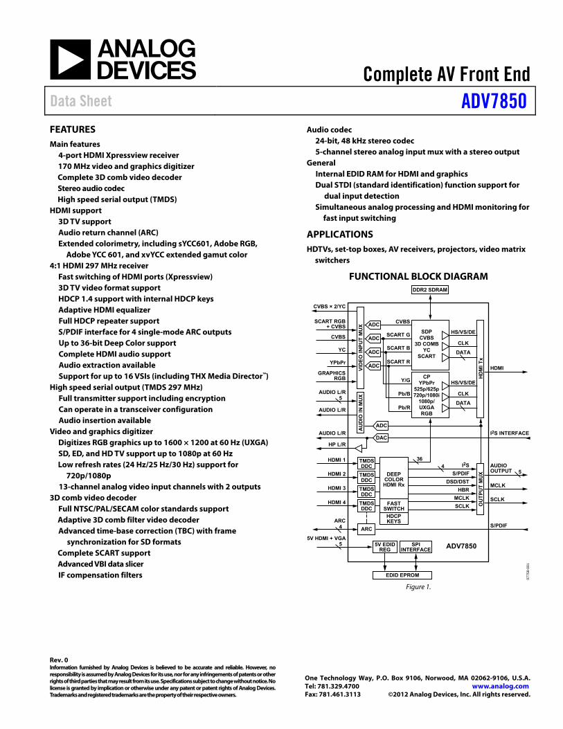
FUNCTIONAL BLOCK DIAGRAM
Figure 1.
0775
8-00
1
ADC
ADC
ADC
ADC
ADC
VID
EO
IN
PU
T M
UX
HD
MI
Tx
CVBS
SCART G
CVBS × 2/YC
SCART RGB+ CVBS
AU
DIO
IN
MU
X
AUDIO L/R
AUDIO L/R
AUDIO L/R
HP L/R
GRAPHICSRGB
CVBS
YC
YPbPr
SCART B
SCART R
Y/G
Pb/B
Pb/R
HDMI
I2S INTERFACE
SDPCVBS
3D COMBYC
SCART
CPYPbPr
525p/625p720p/1080i
1080p/UXGARGB
DDR2 SDRAM
OU
TP
UT
MU
X
HDMI 1
HDMI 2
I2S
S/PDIF
DSD/DST
HBR
MCLK
SCLK
AUDIOOUTPUT
MCLK
SCLK
S/PDIF
36
5
4
5
45
TMDSDDC
TMDSDDC
HDMI 3 TMDSDDC
HDMI 4 TMDSDDC
5V HDMI + VGA5V EDID
REGSPI
INTERFACE
EDID EPROM
ARC
ARC
ADV7850
HS/VS/DE
CLK
DATA
HS/VS/DE
CLK
DATA
DAC
DEEPCOLORHDMI Rx
FASTSWITCH
HDCPKEYS

ADV7850 Data Sheet
Rev. 0 | Page 2 of 32
TABLE OF CONTENTS Features .............................................................................................. 1 Applications ....................................................................................... 1 Functional Block Diagram .............................................................. 1 Revision History ............................................................................... 2 General Description ......................................................................... 3 Detailed Functional Block Diagram .............................................. 4 Specifications ..................................................................................... 5
Electrical Characteristics ............................................................. 5 Power Specifications .................................................................... 6 Analog Specifications ................................................................... 7 Video Specifications ..................................................................... 9 Timing Characteristics .............................................................. 10 Timing Diagrams ........................................................................ 11
Absolute Maximum Ratings .......................................................... 13 Package Thermal Performance ................................................. 13 ESD Caution ................................................................................ 13
Pin Configuration and Function Descriptions ........................... 14 Power Supply Sequencing .............................................................. 24
Power-Up Sequence ................................................................... 24 Power-Down Sequence .............................................................. 24 Power Supply requirements ...................................................... 24
Functional Overview...................................................................... 25 HDMI Receiver ........................................................................... 25 Analog Front End ....................................................................... 25 Standard Definition Processor ................................................. 26 Component Processor ............................................................... 26 VBI Data Processor (VDP) ....................................................... 27 TMDS Output ............................................................................. 27 External Memory Requirements .............................................. 27 Other Features ............................................................................ 27
Audio Overview .............................................................................. 28 Analog Audio MUX Functionality .......................................... 28 Audio Codec Functionality ....................................................... 28
Register Map Architecture ............................................................ 29 Outline Dimensions ....................................................................... 30
Ordering Guide .......................................................................... 30
REVISION HISTORY 5/12—Revision 0: Initial Version

Data Sheet ADV7850
Rev. 0 | Page 3 of 32
GENERAL DESCRIPTIONThe ADV7850 is a high quality, single chip, multiformat video decoder graphics digitizer with an integrated 4:1 multiplexed HDMI® receiver.
This multiformat 3D comb filter decoder supports the conversion of PAL, NTSC, and SECAM standards in the form of a composite or an S-Video input signal into a HDMI output stream. SCART and overlay functionality are enabled by the ability of the ADV7850 to process CVBS and standard definition RGB signals simultaneously.
The ADV7850 contains one main component processor (CP) that processes YPrPb and RGB component formats, including RGB graphics. The ADV7850 can operate in quad HDMI and analog input mode, thus allowing for fast switching between the analog video inputs and HDMI.
The ADV7850 supports the decoding of a component RGB/ YPrPb video signal into a HDMI output stream. The support for component video includes 525i, 625i, 525p, 625p, 720p, 1080i, 1080p, and 1250i standards, as well as many other SMPTE and HD standards.
The ADV7850 supports graphics digitization. The ADV7850 is capable of digitizing RGB graphics signals from VGA to UXGA rates and converting them into an HDMI output stream. Internal EDID RAM is available for one graphics port.
The ADV7850 incorporates a quad input HDMI-compatible receiver that supports all HDTV formats up to 3D 1080p 60 Hz and 2160P 24 Hz.
The ADV7850 supports full HDCP decryption with internal key storage. The ADV7850 features HDCP authentication on all ports simultaneously. The feature allows fast switching between HDMI ports. Sync measurements and status monitoring are also available for all HDMI ports. Each HDMI port has dedi-cated 5 V detect and hot plug assert pins. The HDMI receiver
also includes an integrated equalizer that ensures robust opera-tion of the interface with cable lengths up to 30 meters. The HDMI receiver has advanced audio functionality, such as a mute flag, that prevents audible extraneous noise in the audio output.
In addition, the HDMI receiver incorporates internal EDID support, which can be made available in full power, power-down, and power-off modes. An internal regulator supplies external EDID memory from the HDMI 5 V signal in power- off mode.
The ADV7850 incorporates Xpressview™ fast switching on all HDMI input ports. Using the Analog Devices, Inc., hardware-based HDCP engine that minimizes software overhead, Xpressview technology allows fast switching between any two HDMI input ports in less than 1 second.
The ADV7850 offers a flexible audio output port for the audio data decoded from the HDMI stream. HDMI audio formats, including super audio CD (SACD) via DSD, DST, and HBR are supported.
The ADV7850 also features the single mode audio return channel (ARC) feature. ARC simplifies cabling by combining upstream audio capability in a conventional HDMI cable.
The stereo audio ADC converts analog audio inputs and provides the data to the back end via the HDMI interface. The stereo audio DAC receives I2S data from the back end and converts it to analog audio output. The audio output is available as both high impedance and a driven output, which is suitable for driving headphones directly.
Fabricated in an advanced CMOS process, the ADV7850 is provided in a 19 mm × 19 mm, 425-ball, CSP_BGA, surface-mount, RoHS-compliant package, and is specified over the −20°C to +70°C temperature range.
ADV7850 Data Sheet
Rev. 0 | Page 4 of 32
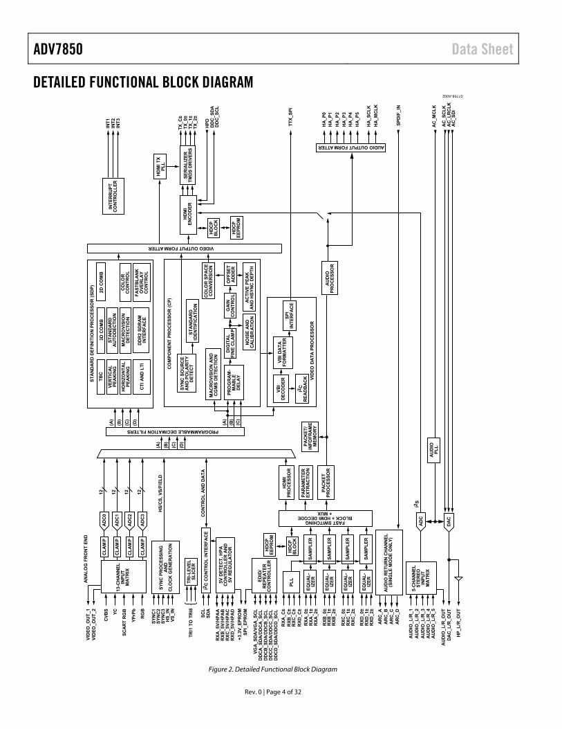
DETAILED FUNCTIONAL BLOCK DIAGRAM
Figure 2. Detailed Functional Block Diagram
07758-A002
AD
C0
CL
AM
P1
2
AD
C1
CL
AM
P1
2
AD
C2
CL
AM
P1
2
AD
C3
CL
AM
P1
2
(A)
(B)
(C)
(D)
(A)
(B)
(C)
HD
CP
EE
PR
OM
PL
L
EQ
UA
L-
IZE
R
EQ
UA
L-
IZE
R
HD
CP
BL
OC
K
SA
MP
LE
R
SA
MP
LE
R
HS
/CS
, V
S/F
IEL
D
CO
NT
RO
L A
ND
DA
TA
PA
RA
ME
TE
RE
XT
RA
CT
ION
PA
CK
ET
PR
OC
ES
SO
R
HD
MI
PR
OC
ES
SO
R
VB
ID
EC
OD
ER
INT
ER
RU
PT
CO
NT
RO
LL
ER
AU
DIO
PR
OC
ES
SO
R
VIDEO OUTPUT FORMATTER
TT
X_S
PI
INT
1IN
T2
AC
TIV
E P
EA
KA
ND
HS
YN
C D
EP
TH
NO
ISE
AN
DC
AL
IBR
AT
ION
OF
FS
ET
AD
DE
R
MA
CR
OV
ISIO
N A
ND
CG
MS
DE
TE
CT
ION
SY
NC
SO
UR
CE
AN
D P
OL
AR
ITY
DE
TE
CTCO
MP
ON
EN
T P
RO
CE
SS
OR
(C
P)
ST
AN
DA
RD
DE
FIN
ITIO
N P
RO
CE
SS
OR
(S
DP
)
2D C
OM
B3D
CO
MB
TB
C
MA
CR
OV
ISIO
ND
ET
EC
TIO
N
VID
EO
_OU
T_2
CV
BS
YC
SC
AR
T R
GB
YP
rPb
RG
B
SY
NC
1
HS
_IN
VS
_IN
TR
I1 T
O T
RI8
SC
LS
DA
DD
CA
_SD
A/D
DC
A_S
CL
DD
CB
_SD
A/D
DC
B_S
CL
RX
A_C
±R
XB
_C±
RX
A_0
±R
XA
_1±
RX
A_2
±
EQ
UA
L-
IZE
RS
AM
PL
ER
RX
C_0
±R
XC
_1±
RX
C_2
±
EQ
UA
L-
IZE
RS
AM
PL
ER
RX
D_0
±R
XD
_1±
RX
D_2
±
RX
B_0
±R
XB
_1±
RX
B_2
±
13-C
HA
NN
EL
INP
UT
MA
TR
IX
AN
AL
OG
FR
ON
T E
ND
SY
NC
PR
OC
ES
SIN
GA
ND
CL
OC
K G
EN
ER
AT
ION
TR
I-L
EV
EL
SL
ICE
R
GA
INC
ON
TR
OL
DIG
ITA
LF
INE
CL
AM
PP
RO
GR
AM
-M
AB
LE
DE
LA
YR
XD
_5V
/HP
AD
RX
C_5
V/H
PA
CR
XB
_5V
/HP
AB
RX
A_5
V/H
PA
A
DD
CC
_SD
A/D
DC
C_S
CL
DD
CD
_SD
A/D
DC
D_S
CL
TX
_C
±T
X_0
±T
X_1
±T
X_2
±
RX
C_C
±R
XD
_C±
SY
NC
2H
DM
I T
XP
LL
SE
RIA
LIZ
ER
TM
DS
DR
IVE
RS
HD
MI
EN
CO
DE
R
5-C
HA
NN
EL
ST
ER
EO
INP
UT
MA
TR
IX
AU
DIO
_L/R
_1
AU
DIO
_L/R
_2
AU
DIO
_L/R
_3
AU
DIO
_L/R
_4
AU
DIO
_L/R
_5
AU
DIO
_L/R
_OU
T
AD
C
DA
CD
AC
_L
/R_O
UT
HP
_L/R
_OU
T
AC
_SC
LK
AC
_LR
CL
KA
C_S
DI
VID
EO
_OU
T_1
SY
NC
3
AU
DIO
RE
TU
RN
CH
AN
NE
L(S
ING
LE
MO
DE
ON
LY
)
AR
C_A
AR
C_B
SP
DIF
_IN
AR
C_C
AR
C_D
AC
_MC
LK
AUDIO OUTPUT FORMATTER
HA
_P0
HA
_P1
HA
_P2
HA
_P3
HA
_P4
HA
_P5
HA
_SC
LK
HA
_MC
LK
SP
I_E
PR
OM
(A)
(B)
(C)
(D)
+3.
3V_E
PR
OM
HP
DD
DC
_SD
AD
DC
_SC
L
VG
A_S
DA
/VG
A_S
CL
INT
3
PROGRAMMABLE DECIMATION FILTERS
DD
R2
SD
RA
MIN
TE
RF
AC
E
ST
AN
DA
RD
AU
TO
DE
CT
ION
VE
RT
ICA
LP
EA
KIN
G
HO
RIZ
ON
TA
LP
EA
KIN
G
CT
I A
ND
LT
IF
AS
TB
LA
NK
OV
ER
LA
YC
ON
TR
OL
CO
LO
RC
ON
TR
OL
5V D
ET
EC
T,
HP
AC
ON
TR
OL
LE
R A
ND
5V R
EG
UL
AT
OR
ED
ID/
RE
PE
AT
ER
CO
NT
RO
LL
ER
I2C
CO
NT
RO
L I
NT
ER
FA
CE
PA
CK
ET
/IN
FO
FR
AM
EM
EM
OR
Y
SP
IIN
TE
RF
AC
E
VB
I D
AT
AF
OR
MA
TT
ER
VID
EO
DA
TA
PR
OC
ES
SO
R
I2C
RE
AD
BA
CK
I2S
AU
DIO
PL
L
ST
AN
DA
RD
IDE
NT
IFIC
AT
ION
CO
LO
R S
PA
CE
CO
NV
ER
SIO
NFAST SWITCHING
BLOCK + HDMI DECODE+ MUX
HD
CP
EE
PR
OM
HD
CP
BL
OC
K

Data Sheet ADV7850
Rev. 0 | Page 5 of 32
SPECIFICATIONS AVDD = 1.8 V ± 5%, VDD to GND = 1.8 V ± 5%, PVDD = 1.8 V ± 5%, TX_AVDD = 1.8 V ± 5%, TX_PVDD = 1.8 V ± 5%, SAVDD = 1.8 V ± 5%, SDVDD = 1.8 V ± 5%, CVDD = 1.8 V ± 5%, DVDDIO = 3.3 V ± 5%, TX_VDD33 = 3.3 V ± 5%, TVDD = 3.3 V ± 5%, AC_AVDD = 3.3 V ± 5%. TMIN to TMAX = −20°C to +70°C, unless otherwise noted.
ELECTRICAL CHARACTERISTICS
Table 1. Parameter Symbol Test Conditions/Comments Min Typ Max Unit STATIC PERFORMANCE
Resolution (Each ADC) N 12 Bits Integral Nonlinearity INL 27 MHz (at a 12-bit level) −3.0 to +8.0 LSB 54 MHz (at a 12-bit level) −3.0 to +8.0 LSB 74.25 MHz (at a 12-bit level) −4.0 to +7.0 LSB 108 MHz (at a 11-bit level) −3.5 to +8.0 LSB 170 MHz (at a 9-bit level) −0.7 to +1.8 LSB Differential Nonlinearity DNL 27 MHz (at a 12-bit level) −0.7 to +0.8 LSB 54 MHz (at a 12-bit level) −0.7 to +0.8 LSB 75 MHz (at a 12-bit level) −0.7 to +0.8 LSB 108 MHz (at a 11-bit level) −0.7 to +0.8 LSB 170 MHz (at a 9-bit level) −0.6 to +0.5 LSB
DIGITAL INPUTS Input High Voltage VIH XTALN and XTALP pins 1.2 V Input Low Voltage VIL XTALN and XTALP pins 0.4 V VIH Other digital inputs 2 V VIL Other digital inputs 0.8 V Input Capacitance CIN 10 pF
HDMI TMDS Differential Pin Capacitance 0.3 pF
DIGITAL INPUTS (5 V TOLERANT)1 Input High Voltage VIH 3.0 V Input Low Voltage VIL 0.8 V Input Current IIN −82 +82 µA
DIGITAL OUTPUTS Output High Voltage VOH 2.4 V Output Low Voltage VOL 0.4 V High Impedance Leakage Current ILEAK DDC_SCL, DDCA_SDA, DDCB_SCL,
DDCB_SDA, DDCC_SCL, DDCC_SDA, DDCD_SCL, DDCD_SDA, VGA_SCL, VGA_SDA, SPDIF_IN, SHARED_EDID
30 µA
ILEAK RXA_5V, RXB_5V, RXC_5V, RXD_5V and VGA_5V
20 µA
ILEAK All other digital pins 10 µA Output Capacitance COUT 20 pF
1 The following pins are 5 V tolerant: HS_IN1/TRI7, HS_IN2/TRI5, VS_IN1/TRI8, VS_IN2/TRI6, DDCA_SCL, DDCA_SDA, DDCB_SCL, DDCB_SDA, DDCC_SCL, DDCC_SDA,
DDCD_SCL, DDCD_SDA, VGA_SCL, VGA_SDA, TX_DDC_SCL, TX_DDC_SDA, RXA_5V, RXB_5V, RXC_5V, RXD_5V, and VGA_5V.
ADV7850 Data Sheet
Rev. 0 | Page 6 of 32
POWER SPECIFICATIONS
Table 2. Parameter Symbol Min Typ Max Unit Test Conditions/Comments POWER REQUIREMENTS
Digital Core Power Supply VDD 1.75 1.8 1.85 V Digital I/O Power Supply DVDDIO 3.14 3.3 3.46 V Memory Interface Analog Power Supply SAVDD 1.71 1.8 1.89 V Memory Interface Digital Power Supply SDVDD 1.71 1.8 1.89 V DPLL Power Supply PVDD 1.71 1.8 1.89 V Video Analog Power Supply AVDD 1.71 1.8 1.89 V Terminator Power Supply TVDD 3.14 3.3 3.46 V Comparator Power Supply CVDD 1.71 1.8 1.89 V Audio Block Supply AC_AVDD 3.14 3.3 3.46 V HDMI Tx Analog Power Supply TX_AVDD 1.71 1.8 1.89 V HDMI Tx Digital Power Supply TX_PVDD 1.71 1.8 1.89 V HDMI Tx PLL Regulator Power Supply TX_VDD33 3.14 3.3 3.46 V
CURRENT CONSUMPTION1, 2, 3 Digital Core Supply Current IVDD 400 440 mA Digital I/O Supply Current IDVDDIO 3 4 mA DPLL Supply Current IPVDD 36 45 mA Video Analog Supply Current IAVDD 270 290 mA Memory Interface Analog Power Supply ISAVDD 4 5 mA Memory Interface Digital Power Supply ISDVDD 15 18 mA Comparator Supply Current ICVDD 300 350 mA Audio Block Supply Current IAC_AVDD 80 84 mA HDMI Tx Analog Supply Current ITX_AVDD 20 25 mA HDMI Tx Digital Supply Current ITX_PVDD 43 50 mA HDMI Tx PLL Regulator Supply Current ITX_VDD33 2 5 mA Terminator Supply Current4 ITVDD 80 85 mA One port connected 280 290 mA Four ports connected Power-Down Currents5 IVDD 1 mA IDVDDIO 1.5 mA IPVDD 0.5 mA IAVDD 0.5 mA ISAVDD 0.5 mA ISDVDD 0.5 mA ITVDD 0.5 mA ICVDD 0.5 mA IAC_AVDD 1 mA ITX_AVDD 2.5 mA ITX_PVDD 0.5 mA ITX_VDD33 0.5 mA Power-Up Time tPWRUP 25 ms
1 All maximum current values are guaranteed by characterization to assist in power supply design. 2 Typical current consumption values are recorded with nominal voltage supply levels, SMPTE bar video pattern, and at room temperature. 3 Maximum current consumption values are recorded with maximum rated voltage supply levels, MoireX video pattern, and at maximum rated temperature. 4 Termination power supply includes TVDD current consumed off chip. 5 Power-down mode entered by setting the I2C Bit POWER_DOWN high.
Data Sheet ADV7850
Rev. 0 | Page 7 of 32
ANALOG SPECIFICATIONS
Table 3. Parameter Test Conditions/Comments Min Typ Max Unit CLAMP CIRCUITRY1
Input Impedance Clamps switched off 10 MΩ Analog (AIN1 to AIN12)
ADC Midscale (CML) 0.91 V ADC Full-Scale Level CML + 0.55 V ADC Zero-Scale Level CML − 0.55 V ADC Dynamic Range 1.1 V Clamp Level (When Locked) Component input, Y signal CML − 0.12 V Component input, Pr signal CML V Component input, Pb signal CML V PC RGB input (R, G, B signals) CML − 0.12 V CVBS input CML − 0.205 V SCART RGB input (R, G, B signals) CML − 0.205 V S-Video input (Y signal) CML − 0.205 V S-Video input (C signal) CML V Large Clamp Source Current SDP only 0.3 mA Large Clamp Sink Current SDP only 0.4 mA Fine Clamp Source Current SDP only 9 μA Fine Clamp Sink Current SDP only 8 μA
AUDIO ADC SECTION2 Number of Channels Stereo pair 1 Channel Full-Scale Input Level 50 µA rms
Resolution 24 Bits Dynamic Range (Stereo Channel)
A-Weighted −60 dBFS with respect to full-scale analog input
90 dB
Total Harmonic Distortion + Noise (Stereo Channel) −3 dBFS with respect to full-scale analog input
−85 dB
Gain Mismatch Left- and right-channel gain mismatch
0.2 dB
Crosstalk (Left to Right, Right to Left) −90 dB Gain Error Input signal = 2.8 V rms −1.1 dB Power Supply Rejection 1 kHz, 300 mV p-p signal at AVDD −89 dB
AUDIO ADC DIGITAL DECIMATOR FILTER CHARACTERISTICS2 At 48 kHz, guaranteed by design Pass Band 22.5 kHz Pass-Band Ripple ±0.0002 dB Stop Band 26.5 kHz Stop-Band Attenuation 100 dB Group Delay 1040 µs
AUDIO DAC SECTION2 Number of Auxiliary Output Channels Stereo pair 1 Channel Resolution 24 Bits Full-Scale Analog Output 1.0 V rms Dynamic Range
A-Weighted −60 dBFS with respect to full-scale code input
93 dB
Total Harmonic Distortion + Noise −3 dBFS with respect to full-scale code input
−89 dB
ADV7850 Data Sheet
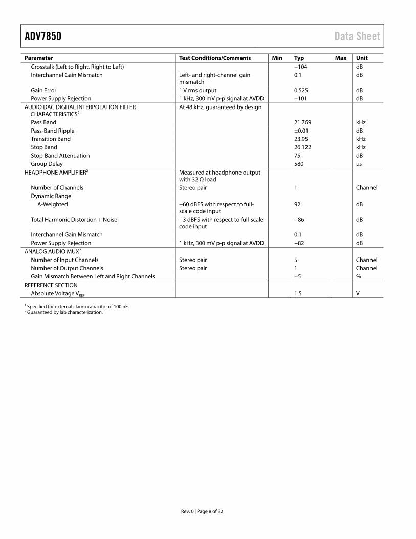
Rev. 0 | Page 8 of 32
Parameter Test Conditions/Comments Min Typ Max Unit Crosstalk (Left to Right, Right to Left) −104 dB Interchannel Gain Mismatch Left- and right-channel gain
mismatch 0.1 dB
Gain Error 1 V rms output 0.525 dB Power Supply Rejection 1 kHz, 300 mV p-p signal at AVDD −101 dB
AUDIO DAC DIGITAL INTERPOLATION FILTER CHARACTERISTICS2
At 48 kHz, guaranteed by design
Pass Band 21.769 kHz Pass-Band Ripple ±0.01 dB Transition Band 23.95 kHz Stop Band 26.122 kHz Stop-Band Attenuation 75 dB Group Delay 580 µs
HEADPHONE AMPLIFIER2 Measured at headphone output with 32 Ω load
Number of Channels Stereo pair 1 Channel Dynamic Range
A-Weighted −60 dBFS with respect to full-scale code input
92 dB
Total Harmonic Distortion + Noise −3 dBFS with respect to full-scale code input
−86 dB
Interchannel Gain Mismatch 0.1 dB Power Supply Rejection 1 kHz, 300 mV p-p signal at AVDD −82 dB
ANALOG AUDIO MUX2 Number of Input Channels Stereo pair 5 Channel Number of Output Channels Stereo pair 1 Channel Gain Mismatch Between Left and Right Channels ±5 %
REFERENCE SECTION Absolute Voltage VREF 1.5 V
1 Specified for external clamp capacitor of 100 nF. 2 Guaranteed by lab characterization.

Data Sheet ADV7850
Rev. 0 | Page 9 of 32
VIDEO SPECIFICATIONS
Table 4. Parameter Symbol Test Conditions/Comments Min Typ Max Unit NONLINEAR SPECIFICATIONS1
Differential Phase DP CVBS input (modulated five-step) 0.5 Degrees Differential Gain DG CVBS input (modulated five-step) 0.6 % Luma Nonlinearity LNL CVBS input (modulated five-step) 0.9 %
NOISE SPECIFICATIONS1 Measured at 27 MHz LLC SNR Unweighted Luma ramp 59 dB SNR Unweighted Luma flat field 60 dB Analog Front-End Crosstalk 60 dB
LOCK TIME SPECIFICATIONS (SDP)2 Horizontal Lock Range ±5 % Vertical Lock Range 40 70 Hz Subcarrier Lock Range fSC ±0.8 kHz Color Lock-In Time 60 Lines Sync Depth Range 20 200 % Color Burst Range 1 200 % Vertical Lock Time 300 ms Horizontal Lock Time 100 Lines
CHROMA SPECIFICATIONS (SDP)1 Chroma Amplitude Error 0.9 % Chroma Phase Error 0.3 Degrees Chroma Luma Intermodulation 0.6 %
1 Guaranteed by lab characterization. 2 Guaranteed by design.
ADV7850 Data Sheet
Rev. 0 | Page 10 of 32
TIMING CHARACTERISTICS Data, SPI, and I2C Timing Characteristics
Table 5. Parameter Symbol Test Conditions/Comments Min Typ Max Unit CLOCK AND CRYSTAL
Crystal Frequency 27 MHz Crystal Frequency Stability ±50 ppm
I2C PORT1 See Figure 3 SCL Frequency 400 kHz SCL Minimum Pulse Width High t1 600 ns SCL Minimum Pulse Width Low t2 1.3 μs Start Condition Hold Time t3 600 ns Start Condition Setup Time t4 600 ns SDA Setup Time t5 100 ns SCL and SDA Rise Time t6 1000 ns SCL and SDA Fall Time t7 300 ns Stop Condition Setup Time t8 0.6 μs
RESET FEATURE Reset Pulse Width 5 ms
HDMI AUDIO I2S PORT, MASTER MODE See Figure 4 HA_SCLK Mark-Space Ratio t15:t16 45:55 45:55 % duty cycle LRCLK2 Data Transition Time t17 End of valid data to negative
HA_SCLK edge 2 ns
LRCLK2 Data Transition Time t18 Negative HA_SCLK edge to start of valid data
2 ns
I2Sx3 Data Transition Time t19 End of valid data to negative HA_SCLK edge
2 ns
I2Sx3 Data Transition Time t20 Negative HA_SCLK edge to start of valid data
2 ns
AUDIO CODEC MASTER CLOCK AC_MCLK Frequency Range fMCLK 4.096 24.576 MHz AC_MCLK Frequency fMCLK 128 × fS Hz
SPI READ AND WRITE OPERATIONS1 See Figure 5, Figure 7, and Figure 8 SCLK Frequency 13.5 MHz Master Mode
TTX_SCLK Falling Edge to CS/TTX_MOSI Valid
t21, t22 3.0 4.1 ns
TTX_MISO Setup Time t23 15.3 ns TTX_MISO Hold Time t24 2.1 ns
Slave Mode CS Falling Edge to TTX_SCLK
Rising Edge t25, t26 4.0 ns
TTX_SCLK Falling Edge to CS Rising Edge
t27, t28 4.0 ns
TTX_MOSI Setup Time t29 1.8 ns TTX_MOSI Hold Time t30 2.7 ns TTX_SCLK Falling Edge to
CS/MOSI Valid t31, t32 7.3 15.5 ns
1 Guaranteed by design. 2 LRCLK is a signal accessible via HA_AP5. 3 I2Sx are signals accessible via Ball HA_AP1 to Ball HA_AP4.
Data Sheet ADV7850
Rev. 0 | Page 11 of 32
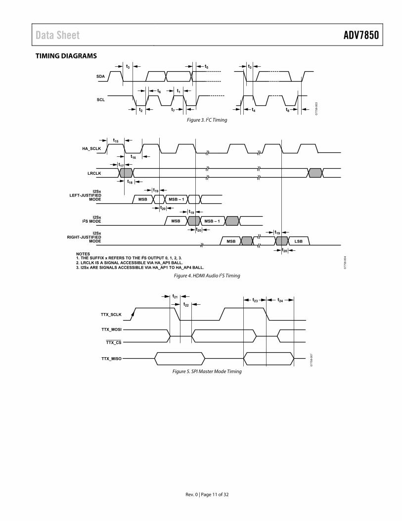
TIMING DIAGRAMS
Figure 3. I2C Timing
Figure 4. HDMI Audio I2S Timing
Figure 5. SPI Master Mode Timing
0775
8-00
3
SDA
SCL
t5 t3
t4 t8
t6
t7t2
t1
t3
HA_SCLK
LRCLK
I2SxLEFT-JUSTIFIED
MODE
I2SxRIGHT-JUSTIFIED
MODE
I2SxI2S MODE
MSB MSB – 1
t15
t16
t17
t19
t20
t18
MSB MSB – 1
LSBMSB
t19
t20 t19
t20NOTES1. THE SUFFIX x REFERS TO THE I2S OUTPUT 0, 1, 2, 3.2. LRCLK IS A SIGNAL ACCESSIBLE VIA HA_AP5 BALL.3. I2Sx ARE SIGNALS ACCESSIBLE VIA HA_AP1 TO HA_AP4 BALL. 07
758-
004
0775
8-00
7
t21
t22
t23 t24
TTX_SCLK
TTX_MOSI
TTX_CS
TTX_MISO

ADV7850 Data Sheet
Rev. 0 | Page 12 of 32
Figure 6. SPI Master Mode Overview
Figure 7. SPI Slave Mode Timing
Figure 8. SPI Slave Mode Overview
TTX_CS
TTX_SCLK
TTX_MOSI
TTX_MISO
23 22 21 ... 3 2 1 0 7 6 5 4 3 2 1
7 6 5 4 3 2 1 0 7 6 5 4 3 2 1 0
0
INSTRUCTION (0x0B) 24-BIT ADDRESS DUMMY BYTE
DATA OUT 1 DATA OUT 2
0775
8-00
8
0775
8-00
9
t29 t31t32
t30
TTX_SCLK
TTX_MOSI
TTX_CS
TTX_MISO
0775
8-01
0
TTX_SCLK
TTX_MOSI
TTX_MISO
TTX_SCLK
TTX_SCLK
TTX_SCLK
CS
1
1
0
0
CPCL
1
0
1
0
CPHA
7 6 5 4 3 2 1 0
7 6 5 4 3 2 1 0
t25
t26
t27
t28
W/R
DEVICE ADDRESS
DUMMY BYTE DATA OUT 0

Data Sheet ADV7850
Rev. 0 | Page 13 of 32
ABSOLUTE MAXIMUM RATINGS Table 6. Parameter Rating AVDD to GND 2.2 V VDD to GND 2.2 V PVDD to GND 2.2 V TX_AVDD to GND 2.2 V TX_PVDD to GND 2.2 V SAVDD to GND 2.2 V SDVDD to GND 2.2 V CVDD to GND 2.2 V DVDDIO to GND 4.0 V TVDD to GND 4.0 V AC_AVDD to GND 4.0 V Maximum Difference Across All 1.8 V
Supplies −0.3 V to +0.3 V
Maximum Difference Across All 3.3 V Supplies
−0.3 V to +0.3 V
Maximum Difference Between 3.3 V Domain Supplies and 1.8 V Domain Supplies
−0.3 V to +2.2 V
Digital Inputs Voltage to GND −0.3 V to DVDDIO + 0.3 V Digital Outputs Voltage to GND −0.3 V to DVDDIO + 0.3 V 5 V Tolerant Digital Inputs to GND1 5.5 V Analog Inputs to GND −0.3V to AVDD + 0.3 V−0.3V
to AC_AVDD + 0.3 V XTALN and XTALP to GND −0.3 V to PVDD + 0.3 V Maximum Junction Temperature (TJ MAX) 125°C Storage Temperature Range −65°C to +150°C Infrared Reflow Soldering (20 sec) 260°C 1 The following inputs are 3.3 V inputs but are 5 V tolerant: HS_IN1/TRI7,
HS_IN2/TRI5, VS_IN1/TRI8, VS_IN2/TRI6, DDCA_SCL, DDCA_SDA, DDCB_SCL, DDCB_SDA, DDCC_SCL, DDCC_SDA, DDCD_SCL, DDCD_SDA, VGA_SCL, VGA_SDA, TX_DDC_SCL, TX_DDC_SDA, RXA_5V, RXB_5V, RXC_5V, RXD_5V and VGA_5V.
Stresses above those listed under Absolute Maximum Ratings may cause permanent damage to the device. This is a stress rating only; functional operation of the device at these or any other conditions above those indicated in the operational section of this specification is not implied. Exposure to absolute maximum rating conditions for extended periods may affect device reliability.
PACKAGE THERMAL PERFORMANCE To reduce power consumption when using the ADV7850, the user is advised to turn off unused sections of the part.
Due to PCB metal variation, and, therefore, variation in PCB heat conductivity, the value of θJA may differ for various PCBs.
The most efficient measurement solution is obtained using the package surface temperature to estimate the die temperature because this eliminates the variance associated with the θJA value.
The maximum junction temperature (TJ MAX) of 125°C must not be exceeded. The following equation calculates the junction tempera-ture using the measured package surface temperature and applies only when no heat sink is used on the device under test (DUT):
( )TOTALJTSJ WΨTT ×+=
where: TS is the package surface temperature (°C). ΨJT = 0.7°C/W for the 425-ball CSP_BGA.
WTOTAL = (PVDD × IPVDD) + (0.4 × TVDD × ITVDD) + (CVDD × ICVDD) + (AVDD × IAVDD) + (VDD × IVDD) + (DVDDIO × IDVDDIO) + (TX_AVDD × ITX_AVDD) + (TX_PVDD × ITX_PVDD) + (SAVDD × ISAVDD) + (SDVDD × ISDVDD) + (TX_VDD33 × ITX_VDD33) + (AC_AVDD × IAC_AVDD)
where 0.4 reflects the 40% of TVDD power that is dissipated on the part itself.
ESD CAUTION

ADV7850 Data Sheet
Rev. 0 | Page 14 of 32
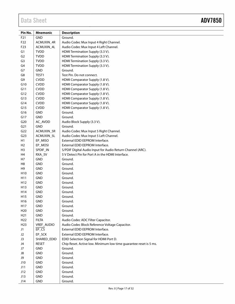
PIN CONFIGURATION AND FUNCTION DESCRIPTIONS
Figure 9. Pin Configuration
0775
8-01
1
1 2 3 4 5 6 7 8 9 10 11 12 13 14 15 16 17 18 19 20 21 22 23
A GND GND GND RXB_2+ RXB_1+ RXB_0+ RXB_C+ ARC_B TVDD RXC_2+ RXC_1+ RXC_0+ RXC_C+ ARC_C GND RXD_2+ RXD_1+ RXD_0+ RXD_C+ ARC_D GND GND GND A
B ARC_A HPA_A GND RXB_2– RXB_1– RXB_0– RXB_C– HPA_B TVDD RXC_2– RXC_1– RXC_0– RXC_C– HPA_C GND RXD_2– RXD_1– RXD_0– RXD_C– HPA_D GND ACMUXOUT_R
ACMUXOUT_L B
C RXA_C+ RXA_C– CVDD GND GND GND GND VDD_EEPROM TVDD TVDD TVDD TVDD TVDD TVDD GND TVDD TVDD TVDD TVDD GND GND ACMUXIN
_1RACMUXIN
_1L C
D RXA_0+ RXA_0– CVDD RXD_5V VGA_5V DDCA_SCL
DDCA_SDA
DDCB_SCL
DDCB_SDA
DDCC_SCL
DDCC_SDA
DDCD_SCL
DDCD_SDA VREG GND VGA_SCL VGA_SDA TVDD AC_AVDD AC_AVDD AC_AVDD ACMUXIN
_2RACMUXIN
_2L D
E RXA_1+ RXA_1– CVDD RXC_5V GND GND ACMUXIN_3R
ACMUXIN_3L E
F RXA_2+ RXA_2– CVDD RXB_5V PLL_LF GND ACMUXIN_4R
ACMUXIN_4L F
G TVDD TVDD TVDD TVDD GND TEST1 CVDD CVDD CVDD CVDD CVDD CVDD CVDD GND GND AC_AVDD GND ACMUXIN_5R
ACMUXIN_5L G
H EP_MISO EP_MOSI SPDIF_IN RXA_5V GND GND GND GND GND GND GND GND GND GND GND GND GND FILTA VREF_AUDIO H
J EP_CS EP_SCK SHARED_EDID RESET GND GND GND GND GND GND GND GND GND GND GND AC_AVDD GND ISET FILTD J
K GND GND DVDDIO DVDDIO VDD GND GND GND GND GND GND GND GND GND GND AC_AVDD AC_AVDDAC_
DACOUT_R
AC_DACOUT_
LK
L HA_AP5 HA_SCLK INT1 SDA VDD GND GND GND GND GND GND GND GND GND GND AC_AVDD AC_AVDD HPOUT_R HPOUT_L L
M HA_AP4 HA_AP3/INT3 INT2 SCL VDD GND GND GND GND GND GND GND GND GND GND AC_AVDD GND GND GND M
N HA_AP2 HA_AP1 AC_MCLK AC_LRCLK VDD GND GND GND GND GND GND GND GND GND GND PVDD PVDD XTALN XTALP N
P HA_AP0 HA_MCLKOUT AC_SDI AC_SCLK VDD GND GND GND GND GND GND GND GND GND GND GND GND GND GND P
R TTX_SCLK
TTX_MOSI
TTX_MISO TTX_CS VDD GND GND GND GND GND GND GND GND GND GND GND GND REFN REFP R
T DVDDIO DVDDIO GND GND VDD GND GND GND GND GND GND GND GND GND GND AVDD AVDD AVDD AVDD T
U TX_AVDD TX_AVDD GND TX_DDC_SCL VDD VDD VDD VDD VDD VDD VDD TEST2 GND GND GND AVIN13 AVIN12 AVIN11 AVIN10 U
V TX_2+ TX_2– GND TX_DDC_SDA AVDD AVDD AVDD AVDD V
W TX_1+ TX_1– GND TX_HPD GND AVOUT2 AVIN9 AVIN8 W
Y TX_0+ TX_0– GND GND A7 A3 A10 BA0 CKE GND DQ6 DQ7 DQ0 DQ8 UDQS SDVDD SAVDD TRI1 TRI2 GND AVOUT1 SYNC3 AVIN7 Y
AA TX_C+ TX_C– TX_AVDD
GND A9 A5 A1 BA1 WE GND DQ4 DQ5 DQ2 DQ11 UDQSN SDVDD GND HS_IN1/TRI7
VS_IN1/TRI8 GND TRI3 HS_IN2/
TRI5VS_IN2/
TRI6 AA
AB GND TX_PVDD
TX_PLVDD
SDVDD A11 A6 A2 CAS RAS VREF SDVDD LDQSN DQ3 DQ10 DQ12 DQ14 GND SYNC1 AVIN3 GND SYNC2 AVIN6 TRI4 AB
AC GND TX_RTERM
TX_VDD33 SDVDD A8 A4 A0 CS CKN CK SDVDD LDQS DQ1 DQ9 DQ15 DQ13 GND AVIN1 AVIN2 GND AVIN4 AVIN5 GND AC
1 2 3 4 5 6 7 8 9 10 11 12 13 14 15 16 17 18 19 20 21 22 23

Data Sheet ADV7850
Rev. 0 | Page 15 of 32
Table 7. Pin Function Descriptions Pin No. Mnemonic Description A1 GND Ground. A2 GND Ground. A3 GND Ground. A4 RXB_2+ Digital Input Channel 2 True of Port B in the HDMI Interface. A5 RXB_1+ Digital Input Channel 1 True of Port B in the HDMI Interface. A6 RXB_0+ Digital Input Channel 0 True of Port B in the HDMI Interface. A7 RXB_C+ Digital Input Clock True of Port B in the HDMI interface. A8 ARC_B Single-Ended Audio Return Channel of Port B in the HDMI Interface. A9 TVDD HDMI Termination Supply (3.3 V). A10 RXC_2+ Digital Input Channel 2 True of Port C in the HDMI Interface. A11 RXC_1+ Digital Input Channel 1 True of Port C in the HDMI Interface. A12 RXC_0+ Digital Input Channel 0 True of Port C in the HDMI Interface. A13 RXC_C+ Digital Input Clock True of Port C in the HDMI Interface. A14 ARC_C Single-Ended Audio Return Channel of Port C in the HDMI Interface. A15 GND Ground. A16 RXD_2+ Digital Input Channel 2 True of Port D in the HDMI Interface. A17 RXD_1+ Digital Input Channel 1 True of Port D in the HDMI Interface. A18 RXD_0+ Digital Input Channel 0 True of Port D in the HDMI Interface. A19 RXD_C+ Digital Input Clock True of Port D in the HDMI Interface. A20 ARC_D Single-Ended Audio Return Channel of Port D in the HDMI Interface. A21 GND Ground. A22 GND Ground. A23 GND Ground. B1 ARC_A Single-Ended Audio Return Channel of Port A in the HDMI Interface. B2 HPA_A Hot Plug Assert for Port A. B3 GND Ground. B4 RXB_2− Digital Input Channel 2 Complement of Port B in the HDMI Interface. B5 RXB_1− Digital Input Channel 1 Complement of Port B in the HDMI Interface. B6 RXB_0− Digital Input Channel 0 Complement of Port B in the HDMI Interface. B7 RXB_C− Digital Input Clock Complement of Port B in the HDMI Interface. B8 HPA_B Hot Plug Assert for Port B. B9 TVDD HDMI Termination Supply (3.3 V). B10 RXC_2− Digital Input Channel 2 Complement of Port C in the HDMI Interface. B11 RXC_1− Digital Input Channel 1 Complement of Port C in the HDMI Interface. B12 RXC_0− Digital Input Channel 0 Complement of Port C in the HDMI Interface. B13 RXC_C− Digital Input Clock Complement of Port C in the HDMI Interface. B14 HPA_C Hot Plug Assert for Port C. B15 GND Ground. B16 RXD_2− Digital Input Channel 2 Complement of Port D in the HDMI Interface. B17 RXD_1− Digital Input Channel 1 Complement of Port D in the HDMI Interface. B18 RXD_0− Digital Input Channel 0 Complement of Port D in the HDMI Interface. B19 RXD_C− Digital Input Clock Complement of Port D in the HDMI Interface. B20 HPA_D Hot Plug Assert for Port D. B21 GND Ground. B22 ACMUXOUT_R Audio Codec Mux Output Right Channel. B23 ACMUXOUT_L Audio Codec Mux Output Left Channel. C1 RXA_C+ Digital Input Clock True of Port A in the HDMI Interface. C2 RXA_C− Digital Input Clock Complement of Port A in the HDMI Interface. C3 CVDD HDMI Comparator Supply (1.8 V). C4 GND Ground. C5 GND Ground. C6 GND Ground.

ADV7850 Data Sheet
Rev. 0 | Page 16 of 32
Pin No. Mnemonic Description C7 GND Ground. C8 VDD_EEPROM External EDID EEPROM Power Supply. C9 TVDD HDMI Termination Supply (3.3 V). C10 TVDD HDMI Termination Supply (3.3 V). C11 TVDD HDMI Termination Supply (3.3 V). C12 TVDD HDMI Termination Supply (3.3 V). C13 TVDD HDMI Termination Supply (3.3 V). C14 TVDD HDMI Termination Supply (3.3 V). C15 GND Ground. C16 TVDD HDMI Termination Supply (3.3 V). C17 TVDD HDMI Termination Supply (3.3 V). C18 TVDD HDMI Termination Supply (3.3 V). C19 TVDD HDMI Termination Supply (3.3 V). C20 GND Ground. C21 GND Ground. C22 ACMUXIN_1R Audio Codec Mux Input 1 Right Channel. C23 ACMUXIN_1L Audio Codec Mux Input 1 Left Channel. D1 RXA_0+ Digital Input Channel 0 True of Port A in the HDMI Interface. D2 RXA_0− Digital Input Channel 0 Complement of Port A in the HDMI Interface. D3 CVDD HDMI Comparator Supply (1.8 V). D4 RXD_5V 5 V Detect Pin for Port D in the HDMI Interface. D5 VGA_5V 5 V Detect I/O for VGA Connector. D6 DDCA_SCL Serial Clock for DDC Bus of Port A. DDCA_SCL is 5 V tolerant. D7 DDCA_SDA Serial Data for DDC Bus of Port A. DDCA_SDA is 5 V tolerant. D8 DDCB_SCL Serial Clock Port for DDC Bus of Port B. DDCB_SCL is 5 V tolerant. D9 DDCB_SDA Serial Data Port for DDC Bus of Port B. DDCB_SDA is 5 V tolerant. D10 DDCC_SCL Serial Clock Port for DDC Bus of Port C. DDCC_SCL is 5 V tolerant. D11 DDCC_SDA Serial Data Port for DDC Bus of Port C. DDCC_SDA is 5 V tolerant. D12 DDCD_SCL Serial Clock Port for DDC Bus of Port D. DDCD_SCL is 5 V tolerant. D13 DDCD_SDA Serial Data Port for DDC Bus of Port D. DDCD_SDA is 5 V tolerant. D14 VREG Voltage Regulator Output. Must be decoupled to GND via 1 µF capacitor. D15 GND Ground. D16 VGA_SCL Serial Clock for VGA Interface. VGA_SCL is 5 V tolerant. D17 VGA_SDA Serial Data for VGA Interface. VGA_SDA is 5 V tolerant. D18 TVDD HDMI Termination Supply (3.3 V). D19 AC_AVDD Audio Block Supply (3.3 V). D20 AC_AVDD Audio Block Supply (3.3 V). D21 AC_AVDD Audio Block Supply (3.3 V). D22 ACMUXIN_2R Audio Codec Mux Input 2 Right Channel. D23 ACMUXIN_2L Audio Codec Mux Input 2 Left Channel. E1 RXA_1+ Digital Input Channel 1 True of Port A in the HDMI Interface. E2 RXA_1− Digital Input Channel 1 Complement of Port A in the HDMI Interface. E3 CVDD HDMI Comparator Supply (1.8 V). E4 RXC_5V 5 V Detect Pin for Port C in the HDMI Interface. E20 GND Ground. E21 GND Ground. E22 ACMUXIN_3R Audio Codec Mux Input 3 Right Channel. E23 ACMUXIN_3L Audio Codec Mux Input 3 Left Channel. F1 RXA_2+ Digital Input Channel 2 True of Port A in the HDMI Interface. F2 RXA_2− Digital Input Channel 2 Complement of Port A in the HDMI Interface. F3 CVDD HDMI Comparator Supply (1.8 V). F4 RXB_5V 5 V Detect Pin for Port B in the HDMI Interface. F20 PLL_LF Loop Filter Ball for Audio Codec PLL.
Data Sheet ADV7850
Rev. 0 | Page 17 of 32
Pin No. Mnemonic Description F21 GND Ground. F22 ACMUXIN_4R Audio Codec Mux Input 4 Right Channel. F23 ACMUXIN_4L Audio Codec Mux Input 4 Left Channel. G1 TVDD HDMI Termination Supply (3.3 V). G2 TVDD HDMI Termination Supply (3.3 V). G3 TVDD HDMI Termination Supply (3.3 V). G4 TVDD HDMI Termination Supply (3.3 V). G7 GND Ground. G8 TEST1 Test Pin. Do not connect. G9 CVDD HDMI Comparator Supply (1.8 V). G10 CVDD HDMI Comparator Supply (1.8 V). G11 CVDD HDMI Comparator Supply (1.8 V). G12 CVDD HDMI Comparator Supply (1.8 V). G13 CVDD HDMI Comparator Supply (1.8 V). G14 CVDD HDMI Comparator Supply (1.8 V). G15 CVDD HDMI Comparator Supply (1.8 V). G16 GND Ground. G17 GND Ground. G20 AC_AVDD Audio Block Supply (3.3 V). G21 GND Ground. G22 ACMUXIN_5R Audio Codec Mux Input 5 Right Channel. G23 ACMUXIN_5L Audio Codec Mux Input 5 Left Channel. H1 EP_MISO External EDID EEPROM Interface. H2 EP_MOSI External EDID EEPROM Interface. H3 SPDIF_IN S/PDIF Digital Audio Input for Audio Return Channel (ARC). H4 RXA_5V 5 V Detect Pin for Port A in the HDMI Interface. H7 GND Ground. H8 GND Ground. H9 GND Ground. H10 GND Ground. H11 GND Ground. H12 GND Ground. H13 GND Ground. H14 GND Ground. H15 GND Ground. H16 GND Ground. H17 GND Ground. H20 GND Ground. H21 GND Ground. H22 FILTA Audio Codec ADC Filter Capacitor. H23 VREF_AUDIO Audio Codec Block Reference Voltage Capacitor. J1 EP_CS External EDID EEPROM Interface.
J2 EP_SCK External EDID EEPROM Interface. J3 SHARED_EDID EDID Selection Signal for HDMI Port D. J4 RESET Chip Reset. Active low. Minimum low time guarantee reset is 5 ms. J7 GND Ground. J8 GND Ground. J9 GND Ground. J10 GND Ground. J11 GND Ground. J12 GND Ground. J13 GND Ground. J14 GND Ground.
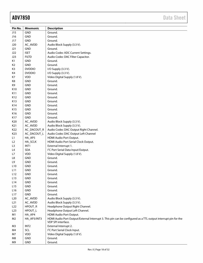
ADV7850 Data Sheet
Rev. 0 | Page 18 of 32
Pin No. Mnemonic Description J15 GND Ground. J16 GND Ground. J17 GND Ground. J20 AC_AVDD Audio Block Supply (3.3 V). J21 GND Ground. J22 ISET Audio Codec ADC Current Settings. J23 FILTD Audio Codec DAC Filter Capacitor. K1 GND Ground. K2 GND Ground. K3 DVDDIO I/O Supply (3.3 V). K4 DVDDIO I/O Supply (3.3 V). K7 VDD Video Digital Supply (1.8 V). K8 GND Ground. K9 GND Ground. K10 GND Ground. K11 GND Ground. K12 GND Ground. K13 GND Ground. K14 GND Ground. K15 GND Ground. K16 GND Ground. K17 GND Ground. K20 AC_AVDD Audio Block Supply (3.3 V). K21 AC_AVDD Audio Block Supply (3.3 V). K22 AC_DACOUT_R Audio Codec DAC Output Right Channel. K23 AC_DACOUT_L Audio Codec DAC Output Left Channel L1 HA_AP5 HDMI Audio Port Output. L2 HA_SCLK HDMI Audio Port Serial Clock Output. L3 INT1 External Interrupt 1. L4 SDA I2C Port Serial Data Input/Output. L7 VDD Video Digital Supply (1.8 V). L8 GND Ground. L9 GND Ground. L10 GND Ground. L11 GND Ground. L12 GND Ground. L13 GND Ground. L14 GND Ground. L15 GND Ground. L16 GND Ground. L17 GND Ground. L20 AC_AVDD Audio Block Supply (3.3 V). L21 AC_AVDD Audio Block Supply (3.3 V). L22 HPOUT_R Headphone Output Right Channel. L23 HPOUT_L Headphone Output Left Channel. M1 HA_AP4 HDMI Audio Port Output. M2 HA_AP3/INT3 HDMI Audio Port Output/External Interrupt 3. This pin can be configured as a TTL output interrupt pin for the
VDP SPI interface. M3 INT2 External Interrupt 2. M4 SCL I2C Port Serial Clock Input. M7 VDD Video Digital Supply (1.8 V). M8 GND Ground. M9 GND Ground.

Data Sheet ADV7850
Rev. 0 | Page 19 of 32
Pin No. Mnemonic Description M10 GND Ground. M11 GND Ground. M12 GND Ground. M13 GND Ground. M14 GND Ground. M15 GND Ground. M16 GND Ground. M17 GND Ground. M20 AC_AVDD Audio Block Supply (3.3 V). M21 GND Ground. M22 GND Ground. M23 GND Ground. N1 HA_AP2 HDMI Audio Port Output. N2 HA_AP1 HDMI Audio Port Output. N3 AC_MCLK Audio Codec/DAC Clock Input. N4 AC_LRCLK Audio DAC Left/Right Clock Input. N7 VDD Video Digital supply (1.8 V). N8 GND Ground. N9 GND Ground. N10 GND Ground. N11 GND Ground. N12 GND Ground. N13 GND Ground. N14 GND Ground. N15 GND Ground. N16 GND Ground. N17 GND Ground. N20 PVDD DPLL Supply (1.8 V). N21 PVDD DPLL Supply (1.8 V). N22 XTALN Crystal Output. N23 XTALP Crystal Input or External Clock Input. P1 HA_AP0 HDMI Audio Port Output. P2 HA_MCLKOUT HDMI Audio Master Clock Output. P3 AC_SDI Audio DAC Data Input. P4 AC_SCLK Audio DAC SCLK Input. P7 VDD Video Digital Supply (1.8 V). P8 GND Ground. P9 GND Ground. P10 GND Ground. P11 GND Ground P12 GND Ground P13 GND Ground P14 GND Ground P15 GND Ground P16 GND Ground P17 GND Ground P20 GND Ground P21 GND Ground P22 GND Ground P23 GND Ground R1 TTX_SCLK VBI Data Interface. R2 TTX_MOSI VBI Data Interface. R3 TTX_MISO VBI Data Interface.
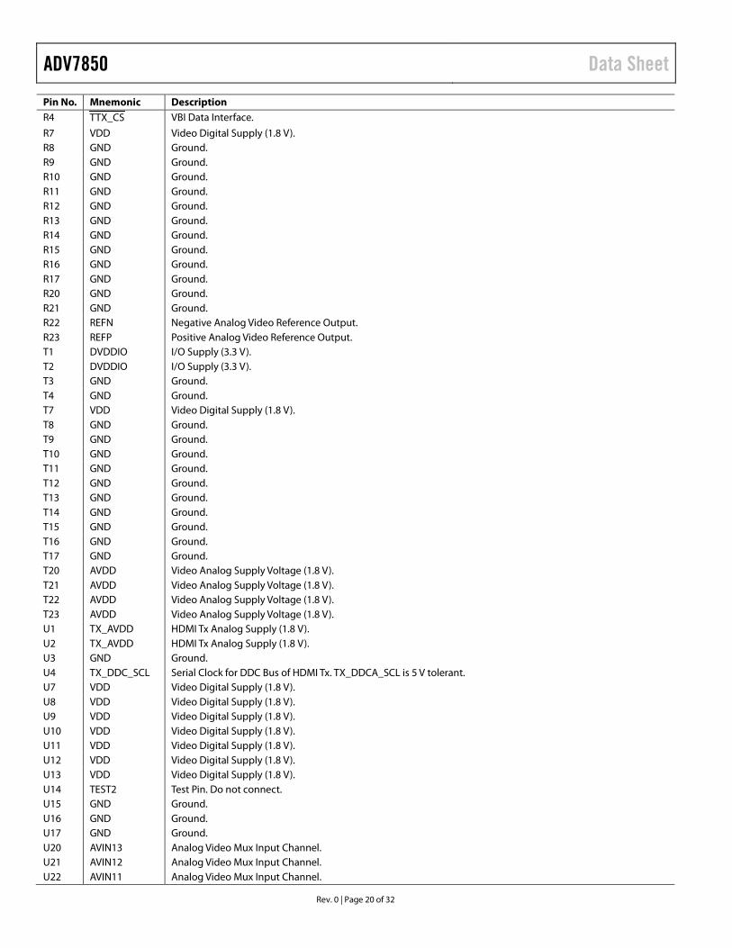
ADV7850 Data Sheet
Rev. 0 | Page 20 of 32
Pin No. Mnemonic Description R4 TTX_CS VBI Data Interface.
R7 VDD Video Digital Supply (1.8 V). R8 GND Ground. R9 GND Ground. R10 GND Ground. R11 GND Ground. R12 GND Ground. R13 GND Ground. R14 GND Ground. R15 GND Ground. R16 GND Ground. R17 GND Ground. R20 GND Ground. R21 GND Ground. R22 REFN Negative Analog Video Reference Output. R23 REFP Positive Analog Video Reference Output. T1 DVDDIO I/O Supply (3.3 V). T2 DVDDIO I/O Supply (3.3 V). T3 GND Ground. T4 GND Ground. T7 VDD Video Digital Supply (1.8 V). T8 GND Ground. T9 GND Ground. T10 GND Ground. T11 GND Ground. T12 GND Ground. T13 GND Ground. T14 GND Ground. T15 GND Ground. T16 GND Ground. T17 GND Ground. T20 AVDD Video Analog Supply Voltage (1.8 V). T21 AVDD Video Analog Supply Voltage (1.8 V). T22 AVDD Video Analog Supply Voltage (1.8 V). T23 AVDD Video Analog Supply Voltage (1.8 V). U1 TX_AVDD HDMI Tx Analog Supply (1.8 V). U2 TX_AVDD HDMI Tx Analog Supply (1.8 V). U3 GND Ground. U4 TX_DDC_SCL Serial Clock for DDC Bus of HDMI Tx. TX_DDCA_SCL is 5 V tolerant. U7 VDD Video Digital Supply (1.8 V). U8 VDD Video Digital Supply (1.8 V). U9 VDD Video Digital Supply (1.8 V). U10 VDD Video Digital Supply (1.8 V). U11 VDD Video Digital Supply (1.8 V). U12 VDD Video Digital Supply (1.8 V). U13 VDD Video Digital Supply (1.8 V). U14 TEST2 Test Pin. Do not connect. U15 GND Ground. U16 GND Ground. U17 GND Ground. U20 AVIN13 Analog Video Mux Input Channel. U21 AVIN12 Analog Video Mux Input Channel. U22 AVIN11 Analog Video Mux Input Channel.

Data Sheet ADV7850
Rev. 0 | Page 21 of 32
Pin No. Mnemonic Description U23 AVIN10 Analog Video Mux Input Channel. V1 TX_2+ Digital Output Channel 2 True of the HDMI Tx. V2 TX_2− Digital Output Channel 2 Complement of the HDMI Tx. V3 GND Ground. V4 TX_DDC_SDA Serial Data for DDC Bus of HDMI Tx. TX_DDCA_SDA is 5 V tolerant. V20 AVDD Video Analog Supply Voltage (1.8 V). V21 AVDD Video Analog Supply Voltage (1.8 V).
V22 AVDD Video Analog Supply Voltage (1.8 V). V23 AVDD Video Analog Supply Voltage (1.8 V). W1 TX_1+ Digital Output Channel 1 True of the HDMI Tx. W2 TX_1− Digital Output Channel 1 Complement of the HDMI Tx. W3 GND Ground. W4 TX_HPD Hot Plug Detect Signal of the HDMI Tx. W20 GND Ground. W21 AVOUT2 Analog Video Mux Output 2. W22 AVIN9 Analog Video Mux Input Channel. W23 AVIN8 Analog Video Mux Input Channel. Y1 TX_0+ Digital Output Channel 0 True of the HDMI Tx. Y2 TX_0− Digital Output Channel 0 Complement of the HDMI Tx. Y3 GND Ground. Y4 GND Ground. Y5 A7 SDRAM Address Line. Y6 A3 SDRAM Address Line. Y7 A10 SDRAM Address Line. Y8 BA0 SDRAM Block Address Signal. Y9 CKE SDRAM Clock Enable. Y10 GND Ground. Y11 DQ6 SDRAM Data Line. Y12 DQ7 SDRAM Data Line. Y13 DQ0 SDRAM Data Line. Y14 DQ8 SDRAM Data Line. Y15 UDQS SDRAM Upper Data Strobe True Signal. Y16 SDVDD Memory Interface Supply. Y17 SAVDD SDRAM Interface Supply. Y18 TRI1 Digital Input Capable of Slicing Bilevel or Trilevel Input from SCART or D-Connector. Y19 TRI2 Digital Input Capable of Slicing Bilevel or Trilevel Input from SCART or D-Connector. Y20 GND Ground. Y21 AVOUT1 Analog Video Mux Output 1. Y22 SYNC3 This is a synchronization on green or luma input (SOG/SOY) used in embedded synchronization mode. Y23 AVIN7 Analog Video Mux Input Channel. AA1 TX_C+ Digital Output Clock True of the HDMI Tx. AA2 TX_C− Digital Output Clock Complement of the HDMI Tx. AA3 TX_AVDD HDMI Tx Analog Supply (1.8 V). AA4 GND Ground. AA5 A9 SDRAM Address Line. AA6 A5 SDRAM Address Line. AA7 A1 SDRAM Address Line. AA8 BA1 SDRAM Block Address Signal. AA9 WE SDRAM Write Enable Signal. AA10 GND Ground. AA11 DQ4 SDRAM Data Line. AA12 DQ5 SDRAM Data Line. AA13 DQ2 SDRAM Data Line.
ADV7850 Data Sheet
Rev. 0 | Page 22 of 32
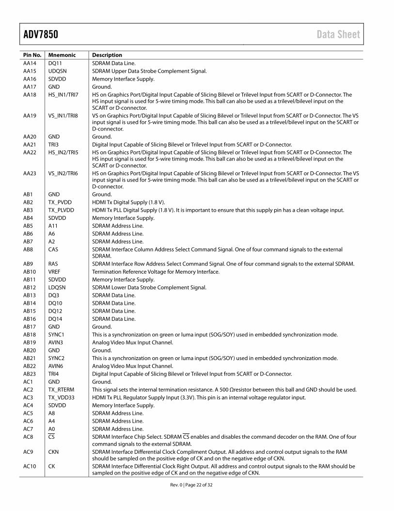
Pin No. Mnemonic Description AA14 DQ11 SDRAM Data Line. AA15 UDQSN SDRAM Upper Data Strobe Complement Signal. AA16 SDVDD Memory Interface Supply. AA17 GND Ground. AA18 HS_IN1/TRI7 HS on Graphics Port/Digital Input Capable of Slicing Bilevel or Trilevel Input from SCART or D-Connector. The
HS input signal is used for 5-wire timing mode. This ball can also be used as a trilevel/bilevel input on the SCART or D-connector.
AA19 VS_IN1/TRI8 VS on Graphics Port/Digital Input Capable of Slicing Bilevel or Trilevel Input from SCART or D-Connector. The VS input signal is used for 5-wire timing mode. This ball can also be used as a trilevel/bilevel input on the SCART or D-connector.
AA20 GND Ground. AA21 TRI3 Digital Input Capable of Slicing Bilevel or Trilevel Input from SCART or D-Connector. AA22 HS_IN2/TRI5 HS on Graphics Port/Digital Input Capable of Slicing Bilevel or Trilevel Input from SCART or D-Connector. The
HS input signal is used for 5-wire timing mode. This ball can also be used as a trilevel/bilevel input on the SCART or D-connector.
AA23 VS_IN2/TRI6 HS on Graphics Port/Digital Input Capable of Slicing Bilevel or Trilevel Input from SCART or D-Connector. The VS input signal is used for 5-wire timing mode. This ball can also be used as a trilevel/bilevel input on the SCART or D-connector.
AB1 GND Ground. AB2 TX_PVDD HDMI Tx Digital Supply (1.8 V). AB3 TX_PLVDD HDMI Tx PLL Digital Supply (1.8 V). It is important to ensure that this supply pin has a clean voltage input. AB4 SDVDD Memory Interface Supply. AB5 A11 SDRAM Address Line. AB6 A6 SDRAM Address Line. AB7 A2 SDRAM Address Line. AB8 CAS SDRAM Interface Column Address Select Command Signal. One of four command signals to the external
SDRAM. AB9 RAS SDRAM Interface Row Address Select Command Signal. One of four command signals to the external SDRAM. AB10 VREF Termination Reference Voltage for Memory Interface. AB11 SDVDD Memory Interface Supply. AB12 LDQSN SDRAM Lower Data Strobe Complement Signal. AB13 DQ3 SDRAM Data Line. AB14 DQ10 SDRAM Data Line. AB15 DQ12 SDRAM Data Line. AB16 DQ14 SDRAM Data Line. AB17 GND Ground. AB18 SYNC1 This is a synchronization on green or luma input (SOG/SOY) used in embedded synchronization mode. AB19 AVIN3 Analog Video Mux Input Channel. AB20 GND Ground. AB21 SYNC2 This is a synchronization on green or luma input (SOG/SOY) used in embedded synchronization mode. AB22 AVIN6 Analog Video Mux Input Channel. AB23 TRI4 Digital Input Capable of Slicing Bilevel or Trilevel Input from SCART or D-Connector. AC1 GND Ground. AC2 TX_RTERM This signal sets the internal termination resistance. A 500 Ωresistor between this ball and GND should be used. AC3 TX_VDD33 HDMI Tx PLL Regulator Supply Input (3.3V). This pin is an internal voltage regulator input. AC4 SDVDD Memory Interface Supply. AC5 A8 SDRAM Address Line. AC6 A4 SDRAM Address Line. AC7 A0 SDRAM Address Line. AC8 CS SDRAM Interface Chip Select. SDRAM CS enables and disables the command decoder on the RAM. One of four
command signals to the external SDRAM. AC9 CKN SDRAM Interface Differential Clock Compliment Output. All address and control output signals to the RAM
should be sampled on the positive edge of CK and on the negative edge of CKN. AC10 CK SDRAM Interface Differential Clock Right Output. All address and control output signals to the RAM should be
sampled on the positive edge of CK and on the negative edge of CKN.
Data Sheet ADV7850
Rev. 0 | Page 23 of 32
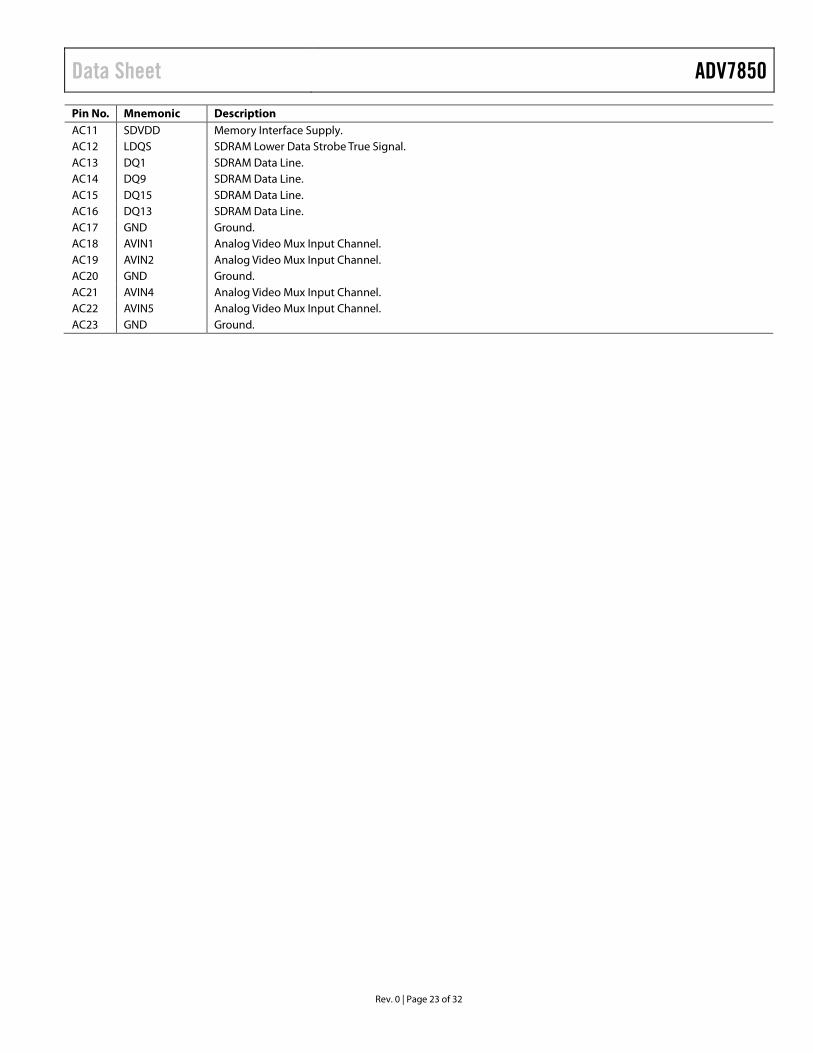
Pin No. Mnemonic Description AC11 SDVDD Memory Interface Supply. AC12 LDQS SDRAM Lower Data Strobe True Signal. AC13 DQ1 SDRAM Data Line. AC14 DQ9 SDRAM Data Line. AC15 DQ15 SDRAM Data Line. AC16 DQ13 SDRAM Data Line. AC17 GND Ground. AC18 AVIN1 Analog Video Mux Input Channel. AC19 AVIN2 Analog Video Mux Input Channel. AC20 GND Ground. AC21 AVIN4 Analog Video Mux Input Channel. AC22 AVIN5 Analog Video Mux Input Channel. AC23 GND Ground.
ADV7850 Data Sheet
Rev. 0 | Page 24 of 32
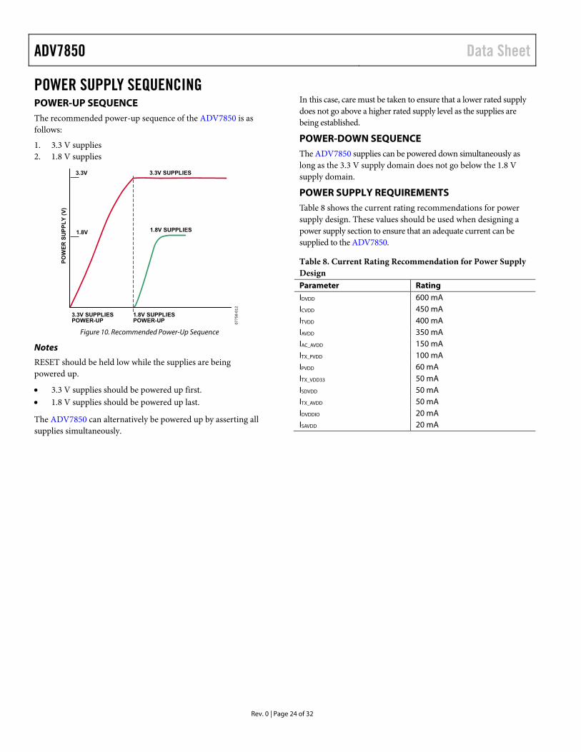
POWER SUPPLY SEQUENCING POWER-UP SEQUENCE The recommended power-up sequence of the ADV7850 is as follows:
1. 3.3 V supplies 2. 1.8 V supplies
Figure 10. Recommended Power-Up Sequence
Notes
RESET should be held low while the supplies are being powered up.
3.3 V supplies should be powered up first. 1.8 V supplies should be powered up last.
The ADV7850 can alternatively be powered up by asserting all supplies simultaneously.
In this case, care must be taken to ensure that a lower rated supply does not go above a higher rated supply level as the supplies are being established.
POWER-DOWN SEQUENCE The ADV7850 supplies can be powered down simultaneously as long as the 3.3 V supply domain does not go below the 1.8 V supply domain.
POWER SUPPLY REQUIREMENTS Table 8 shows the current rating recommendations for power supply design. These values should be used when designing a power supply section to ensure that an adequate current can be supplied to the ADV7850.
Table 8. Current Rating Recommendation for Power Supply Design Parameter Rating IDVDD 600 mA ICVDD 450 mA ITVDD 400 mA IAVDD 350 mA IAC_AVDD 150 mA ITX_PVDD 100 mA IPVDD 60 mA ITX_VDD33 50 mA ISDVDD 50 mA ITX_AVDD 50 mA IDVDDIO 20 mA ISAVDD 20 mA
0775
8-01
2
3.3V SUPPLIESPOWER-UP
PO
WE
R S
UP
PL
Y (
V)
3.3V SUPPLIES
1.8V SUPPLIES
1.8V SUPPLIESPOWER-UP
3.3V
1.8V

Data Sheet ADV7850
Rev. 0 | Page 25 of 32
FUNCTIONAL OVERVIEW HDMI RECEIVER The ADV7850 front end incorporates a 4:1 multiplexed HDMI receiver with Xpressview fast switching technology and support for HDMI features including ARC and 3D TV. Building on the feature set of Analog Devices existing HDMI devices, the ADV7850 also offers support for all HDTV formats up to 3D 1080p at 60 Hz and 2160p at 24 Hz. Xpressview fast switching technology, using the Analog Devices hardware-based HDCP engine that minimizes software overhead, allows switching between any two input ports in less than 1 second.
With the inclusion of HDCP 1.4, the ADV7850 can receive encrypted video content. The HDMI interface of the ADV7850 allows for authentication of a video receiver, decryption of encoded data at the receiver, and renewal of that authentication during transmission, as specified by the HDCP 1.4 protocol. Repeater support is also offered by the ADV7850.
The ADV7850 supports the audio return channel feature. There is a dedicated S/PDIF input on which audio can be received for retransmission on the HDMI input. Wide ranges of 3D video formats are supported, including frame packing up to 3D 1080p at 60 Hz and 2160p at 24 Hz.
The HDMI receiver incorporates active equalization of the HDMI data signals. This equalization compensates for the high frequency losses inherent in HDMI and DVI cabling, especially at longer lengths and higher frequencies. It is capable of equaliz-ing for cable lengths up to 30 meters to achieve robust receiver performance at even the highest HDMI data rates.
The HDMI receiver offers advanced audio functionality. It sup-ports multichannel I2S audio for up to eight channels. It also supports a six-DSD channel interface with each channel carry-ing an oversampled 1-bit representation of the audio signal as delivered on SACD. The ADV7850 can also receive HBR audio packet streams and outputs them through the HBR interface in an S/PDIF format conforming to the IEC 60958 standard.
The receiver contains an audio mute controller that can detect a variety of conditions that may result in audible extraneous noise in the audio output. On detection of these conditions, the audio signal can be muted to prevent audio clicks or pops.
HDMI receiver features include:
• 4:1 multiplexed HDMI receiver • HDMI, ARC, and 3D format support, DVI 1.0 • 297 MHz HDMI receiver • Integrated equalizer • High-bandwidth Digital Content Protection (HDCP 1.4)
on background ports • Internal HDCP keys • 36-/30-bit Deep Color support • PCM, HBR, DSD, and DST audio packet support • Repeater support
• Internal E-EDID RAM • Hot plug assert output pin for each HDMI port
ANALOG FRONT END The ADV7850 analog front end comprises four 170 MHz, 12-bit ADCs that digitize the analog video signal before applying it to the standard definition processor (SDP) or component processor (CP).
The front end also includes a 13-channel input mux that enables multiple video signals to be applied to the ADV7850 without the requirement of an external mux.
Current and voltage clamp control loops ensure that any dc offsets are set properly for the video signal. The clamps are positioned in front of each ADC to ensure that the video signal remains within the range of the converter.
The ADCs are configured to run up to 4× oversampling mode when decoding composite, S-Video, or SCART inputs. For component 525i, 625i, 525p, and 625p sources, 4× oversampling is performed. Higher frequency video standards can be 2× or 1× oversampled. Oversampling the video signals reduces the cost and complexity of external antialiasing filters with the benefit of an increased signal-to-noise ratio (SNR).
Optional internal antialiasing filters with programmable bandwidth are positioned in front of each ADC. These filters can be used to band-limit video signals, removing spurious out-of-band noise.
The ADV7850 can support the simultaneous processing of CVBS and RGB standard definition signals to enable SCART compatibility and overlay functionality. A combination of CVBS and RGB inputs can be mixed with the output under the control of I2C registers.
Analog front-end features include:
• Four 170 MHz, 12-bit NSV ADCs that enable 10-bit (SD)/ 12-bit (CP) video decoding
• 13-channel analog input mux that enables multiple source connections without the requirement of an external mux
• Four current and voltage clamp control loops that ensure any dc offsets are set properly for the video signal
• SCART functionality and SD RGB overlay on CVBS controlled by fastblank input
• SCART source switching detection through the TRI1 to TRI8 inputs
• Four programmable antialiasing filters

ADV7850 Data Sheet
Rev. 0 | Page 26 of 32
STANDARD DEFINITION PROCESSOR The SDP is capable of decoding a large selection of baseband video signals in composite, S-Video, and 525i/625i component formats. The video standards supported by the SDP include PAL, PAL 60, PAL M, PAL N, PAL NC, NTSC M/J, NTSC 4.43, and SECAM. The ADV7850 can automatically detect the video standard and process it accordingly.
The SDP has a 3D temporal comb filter and a five-line adaptive 2D comb filter that gives superior chrominance and luminance separation when decoding a composite video signal. This highly adaptive filter automatically adjusts its processing mode according to the video standard and signal quality with no user intervention required. The SDP has an IF filter block that compensates for attenuation in the high frequency chroma spectrum due to a tuner SAW filter. The SDP has specific luminance and chrominance parameter controls for brightness, contrast, saturation, and hue.
The ADV7850 implements a patented Adaptive Digital Line Length Tracking (ADLLT™) algorithm to track varying video line lengths from sources such as a VCR. ADLLT enables the ADV7850 to track and decode poor quality video sources (such as VCRs) and noisy sources (such as tuner outputs, VCR players, and camcorders). Frame TBC ensures stable clock synchroniza-tion between the decoder and the downstream devices.
The SDP also contains both a luma transient improvement (LTI) block and a chroma transient improvement (CTI) block. These increase the edge rate on the luma and chroma transitions, resulting in a sharper video image.
The SDP has a Macrovision® detection circuit that allows Type I, Type II, and Type III Macrovision protection levels. The decoder is also fully robust to all Macrovision signal inputs.
SDP features include:
• Advanced adaptive 3D comb (using the external DDR2 memory)
• Adaptive 2D five-line comb filters for NTSC and PAL that give superior chrominance and luminance separation for composite video
• Full automatic detection and autoswitching of all worldwide standards (PAL, NTSC, and SECAM)
• Automatic gain control with white peak mode that ensures the video is always processed without loss of the video processing range
• Proprietary architecture for locking to weak, noisy, and unstable sources from VCRs and tuners
• IF filter block that compensates for high frequency luma attenuation due to tuner SAW filter
• LTI and CTI • Vertical and horizontal programmable luma peaking filters • 4× oversampling (54 MHz) for CVBS, and S-Video modes • Free-run output mode that provides stable timing when no
video input is present or video lock is lost • Internal color bar test pattern
• Advanced TBC with frame synchronization, which ensures nominal clock and data for nonstandard input
• Color controls that include hue, brightness, saturation, and contrast
COMPONENT PROCESSOR The CP section of the ADV7850 is capable of decoding and digitizing a wide range of component video formats in any color space. Component video standards supported by the CP include 525i, 625i, 525p, 625p, 720p, 1080i, 1080p, 1250i, VGA up to UXGA at 60 Hz, and many other standards.
The any-to-any, 3 × 3 CSC matrix is placed between the analog front end and the CP section. This enables YPbPr-to-RGB and RGB-to-YCbCr conversions. Many other standards of color space can be implemented using the color space converter.
The CP section contains circuitry to enable the detection of Macrovision encoded YPbPr signals for 525i, 625i, 525p, and 625p. It is designed to be fully robust when decoding these types of signals.
CP features include:
• 525i, 625i, 525p, 625p, 720p, 1080i, 1080p, and many other HDTV formats are supported
• Supports 720p at 24 Hz/25 Hz formats • Manual adjustments including gain (contrast), offset
(brightness), hue, and saturation • Support for analog component YPbPr and RGB video
formats with embedded synchronization, composite synchronization, or separate HS and VS
• Any-to-any, 3 × 3 CSC matrix that supports YCbCr-to-RGB and RGB-to-YCbCr, fully programmable or preprogrammable configurations
• Synchronization source polarity detector (SSPD) that determines the source and polarity of the synchronization signals that accompany the input video
• Macrovision copy protection detection on component formats (525i, 625i, 525p, and 625p)
• Free-run output mode that provides stable timing when no video input is present or video lock is lost
• Arbitrary pixel sampling support for nonstandard video sources
• 170 MHz conversion rate, which supports RGB input resolutions up to 1600 × 1200 at 60 Hz
• Automatic or manual clamp-and-gain controls for graphics modes
• 32-phase ADC DLL that allows optimum pixel clock sampling
• Automatic detection of synchronization source and polarity by SSPD block
• Standard identification enabled by STDI block • RGB that can be color space converted to YCbCr and
decimated to a 4:2:2 format for video-centric back-end IC interfacing

Data Sheet ADV7850
Rev. 0 | Page 27 of 32
VBI DATA PROCESSOR (VDP) VBI extraction of Teletext, CC, WSS, CGMS, PDC, UTC, VPS, GEMSTAR, and VITC data is performed by the VBI data processor of the ADV7850 at interlaced, progressive, and high definition scanning rates. The data extracted can be read back over the SPI interface.
TMDS OUTPUT The ADV7850 incorporates a 297 MHz TMDS output. This interface is designed to connect to any internal IC with an HDMI or DVI input port.
The digital video interface contains an HDMI and a DVI 1.0-compatible transmitter, and supports all HDTV formats up to 3D 1080p at 60 Hz and 2160p at 24 Hz. The ADV7850 transmitter fully supports programmable AVI InfoFrames. With the inclusion of HDCP, the ADV7850 transmitter allows the secure transmission of protected content as specified by the HDCP protocol. The ADV7850 transmitter also fully supports EDID read operations.
The ADV7850 TMDS output supports the audio mode received from the HDMI receiver, that is, PCM, HBR, DSD, and DST.
EXTERNAL MEMORY REQUIREMENTS The ADV7850 requires an external SDRAM for 3D comb and frame TBC. The ADV7850 supports DDR2 memories.
Double Data Rate 2 (DDR2)
The ADV7850 can use DDR2 external memory to simultane-ously provide 3D comb and frame TBC operation.
It requires a minimum memory of 128 Mb with a speed grade of 200 MHz at CAS latency (CL) 3.
The recommended DDR2 memory compatible with the ADV7850 include the MT47H32M16HR-25E:G from Micron Technology, Inc.
OTHER FEATURES The ADV7850 has one I2C host port interface.
The ADV7850 has two programmable interrupt request output pins, INT1 and INT2. It also features a number of low power modes and a full power-down mode. The ADV7850 contains an internal power regulator to accommodate power-off mode. In this mode, the ADV7850 is powered from the 5 V supply of the HDMI/VGA cable connected to a source device or devices. In this mode, EDID can be read over an HDMI/VGA DDC link.
The ADV7850 is provided in a 19 mm × 19 mm, RoHS-compliant CSP_BGA package and is specified over the −20°C to +70°C temperature range.
For more detailed product information about the ADV7850, contact your local Analog Devices sales office.

ADV7850 Data Sheet
Rev. 0 | Page 28 of 32
AUDIO OVERVIEW
Figure 11. Audio Block
The ADV7850 supports an audio codec comprising a stereo ADC and a stereo DAC. A 5:1 stereo mux is placed in front of the ADC input. The DAC output is available as a line level output and is passed through an internal headphone amplifier. The integrated headphone amplifier eliminates the need for an external amplifier when driving headphones.
ANALOG AUDIO MUX FUNCTIONALITY The ADV7850 has five stereo analog audio inputs and one stereo analog output. Any one of the stereo inputs can be connected to the stereo ADC, and any one of the inputs can be connected to the stereo output. In the case of the analog output, the ADV7850 also supports mono in-stereo output. The I/O connectivity is shown in Table 9.
Table 9. Analog Audio Inputs to ADC and Analog Audio Outputs Connection Capability
Mux Input Mux Output ADC Input
Left Right Left Right
1 Left OK OK OK N/A Right OK OK N/A OK
2 Left OK OK OK N/A Right OK OK N/A OK
3 Left OK OK OK N/A Right OK OK N/A OK
4 Left OK OK OK N/A Right OK OK N/A OK
5 Left OK OK OK N/A Right OK OK N/A OK
The ADV7850 is designed to use a combination of internal and external resistances. Measured from the system audio input connector, the total nominal input impedance is 32.1 kΩ. All analog system audio inputs are designed to support 2.8 V rms audio input. Figure 12 shows a high level overview of the implementation.
The input level at the analog audio input pins on the ADV7850 is 880 mV rms. However, the ADV7850 incorporates a gain stage to restore the mux output level to 1.0 V rms. An external line driver is required to restore the audio output signals to the SCART specification of 2.8 V rms. Analog audio mux output signals are inverted with respect to mux input signals.
Figure 12. High Level Overview of Analog Audio Input/Output Configuration
A factory calibration is applied during final test to ensure that the gain through the mux circuit remains within ±5%. Calibra-tion is also applied to the ADC reference current to ensure that the code swing from the ADC remains within ±5% across the part for a given input. External impedances with a tolerance of ±1% are required.
AUDIO CODEC FUNCTIONALITY The ADV7850 audio codec requires an external MCLK. For MCLK with a frequency of 6.144 MHz, 12.288 MHz, or 24.576 MHz, the ADC and DAC sample rate is 48 kHz. If the MCLK is reduced to 5.6448 MHz, 11.2896 MHz, or 22.5792 MHz, the ADC and DAC sample rate reduces to 44.1 kHz.
The bandwidth of the digital filter is sufficient so that 20 kHz pass band is maintained in this mode. The 32 kHz sampling is also possible but with pass-band reduction.
The system controller must set an I2C control to select the correct mode of operation for the internal PLL so that it always generates an internal MCLK of 6.144 MHz. A fixed oversample rate of 128× is implemented.
The word depth of both the ADC and DAC is 24 bits. The ADC and DAC have independent LRCLK and SCLK signals but use a common MCLK.
The ADC supports I2S mode, providing LRCLK, SCLK, and I2S signals. These signals are sent to the HDMI Tx and embedded into the HDMI stream.
The DAC supports I2S mode. The LRCLK, SCLK, and data signals must be provided by the back-end SOC and must be frequency locked with the MCLK but can be phase independ-ent. The output level is 1 V rms full scale.
There is one stereo headphone amplifier output capable of driving 32 Ω loads at 1 V rms. The headphone output incorporates circuitry to suppress pop/click sounds during power-on/off cycle.
0775
8-01
3
AUDIO_L/R_1AUDIO_L/R_2AUDIO_L/R_3AUDIO_L/R_4AUDIO_L/R_5
AUDIO_L/R_OUT
ADC
DACDAC_L/R_OUT
HP_L/R_OUT
AC_SCLKAC_LRCLKAC_SDI
AC_MCLK
TO HDMITx BLOCK
AUDIOPLL
I2S5-CHANNELSTEREO
INPUTMATRIX
0775
8-01
4
ADV7850
2.8 V rms INPUT
2.8 V rms INPUT
2.8 V rms INPUT
2.8 V rms INPUT
2.8 V rms INPUT
MUX OUTPUT
INTERNALIMPEDANCE
10.1kΩ
10.1kΩ
10.1kΩ
10.1kΩ
EXTERNALIMPEDANCE
22kΩ
22kΩ
22kΩ
22kΩ
22kΩ 10.1kΩ
ADC
MU
X
Data Sheet ADV7850
Rev. 0 | Page 29 of 32
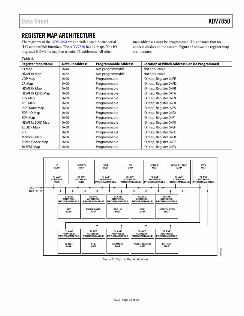
REGISTER MAP ARCHITECTURE The registers of the ADV7850 are controlled via a 2-wire serial (I2C-compatible) interface. The ADV7850 has 17 maps. The IO map and HDMI Tx map has a static I2C addresses. All other
map addresses must be programmed. This ensures that no address clashes on the system. Figure 13 shows the register map architecture.
Table 5. Register Map Name Default Address Programmable Address Location at Which Address Can Be Programmed IO Map 0x40 Not programmable Not applicable HDMI Tx Map 0xB8 Not programmable Not applicable VDP Map 0x00 Programmable IO map, Register 0xFE CP Map 0x00 Programmable IO map, Register 0xFD HDMI Rx Map 0x00 Programmable IO map, Register 0xFB HDMI Rx EDID Map 0x00 Programmable IO map, Register 0xFA KSV Map 0x00 Programmable IO map, Register 0xF9 AFE Map 0x00 Programmable IO map, Register 0xF8 InfoFrame Map 0x00 Programmable IO map, Register 0xF5 SDP_IO Map 0x00 Programmable IO map, Register 0xF2 SDP Map 0x00 Programmable IO map, Register 0xF1 HDMI Tx EDID Map 0x00 Programmable IO map, Register 0xF0 Tx UDP Map 0x00 Programmable IO map, Register 0xEF VFE 0x00 Programmable IO map, Register 0xEC Memory Map 0x00 Programmable IO map, Register 0xEB Audio Codec Map 0x00 Programmable IO map, Register 0xE7 Tx TEST Map 0x00 Programmable IO map, Register 0xE3
Figure 13. Register Map Architecture
IOMAP
SLAVEADDRESS:
0x40
HDMI TxMAP
SLAVEADDRESS:
0xB8
VDPMAP
SLAVEADDRESS:
PROGRAMMABLE
CPMAP
SLAVEADDRESS:
PROGRAMMABLE
HDMI RxMAP
SLAVEADDRESS:
PROGRAMMABLE
AFEMAP
SLAVEADDRESS:
PROGRAMMABLE
INFOFRAMEMAP
SLAVEADDRESS:
PROGRAMMABLE
SDP_IOMAP
SLAVEADDRESS:
PROGRAMMABLE
SDPMAP
SLAVEADDRESS:
PROGRAMMABLE
HDMI Tx EDIDMAP
SLAVEADDRESS:
PROGRAMMABLE
Tx UDPMAP
SLAVEADDRESS:
PROGRAMMABLE
VFEMAP
SLAVEADDRESS:
PROGRAMMABLE
MEMORYMAP
SLAVEADDRESS:
PROGRAMMABLE
AUDIO CODECMAP
SLAVEADDRESS:
PROGRAMMABLE
Tx TESTMAP
SLAVEADDRESS:
PROGRAMMABLE
HDMI Rx EDIDMAP
SLAVEADDRESS:
PROGRAMMABLE
KSVMAP
SLAVEADDRESS:
PROGRAMMABLE
SCLSDA
0775
8-01
5
ADV7850 Data Sheet
Rev. 0 | Page 30 of 32
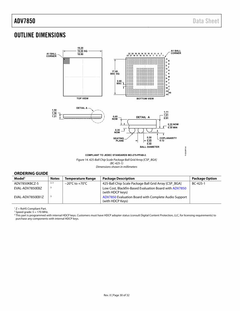
OUTLINE DIMENSIONS
Figure 14. 425-Ball Chip Scale Package Ball Grid Array [CSP_BGA]
(BC-425-1) Dimensions shown in millimeters
ORDERING GUIDE Model1 Notes Temperature Range Package Description Package Option ADV7850KBCZ-5 2, 3 −20°C to +70°C 425-Ball Chip Scale Package Ball Grid Array [CSP_BGA] BC-425-1 EVAL-ADV7850EBZ 3 Low Cost, Blackfin-Based Evaluation Board with ADV7850
(with HDCP keys)
EVAL-ADV7850EB1Z 3 ADV7850 Evaluation Board with Complete Audio Support (with HDCP Keys)
1 Z = RoHS Compliant Part. 2 Speed grade: 5 = 170 MHz. 3 This part is programmed with internal HDCP keys. Customers must have HDCP adopter status (consult Digital Content Protection, LLC, for licensing requirements) to
purchase any components with internal HDCP keys.
AB
CD
EF
GH
JK
LM
NP
R
151714
1312
1110
98
76
54
32
1
17.60BSC SQ
161921
182023
22
TU
VW
YAA
ABAC
0.65NOM
0.35NOM
1.501.361.21
1.111.010.91
COMPLIANT TO JEDEC STANDARDS MO-275-PPAB-2. 11-2
2-2
011
-A
0.500.450.40
19.2019.00 SQ18.80
COPLANARITY0.12
BOTTOM VIEW
DETAIL A
TOP VIEW
0.35 NOM0.30 MIN
BALL DIAMETER
SEATINGPLANE
A1 BALLCORNER
A1 BALLCORNER
DETAIL A
0.80BSC

Data Sheet ADV7850
Rev. 0 | Page 31 of 32
NOTES
ADV7850 Data Sheet
Rev. 0 | Page 32 of 32
NOTES
©2012 Analog Devices, Inc. All rights reserved. Trademarks and registered trademarks are the property of their respective owners. D07758-0-5/12(0)