complete digital design
TRANSCRIPT


COMPLETE DIGITAL DESIGN
-Balch.book Page i Thursday, May 15, 2003 3:46 PM

This page intentionally left blank.
COMPLETE DIGITAL DESIGN
A Comprehensive Guide to Digital Electronics
and Computer System Architecture
Mark Balch
McGRAW-HILL
New York Chicago San Francisco
Lisbon London Madrid Mexico City Milan
New Delhi San Juan Seoul Singapore
Sydney Toronto
-Balch.book Page iii Thursday, May 15, 2003 3:46 PM

Copyright © 2003 by The McGraw-Hill Companies, Inc. All rights reserved. Manufactured in the United States ofAmerica. Except as permitted under the United States Copyright Act of 1976, no part of this publication may bereproduced or distributed in any form or by any means, or stored in a database or retrieval system, without the priorwritten permission of the publisher.
0-07-143347-3
The material in this eBook also appears in the print version of this title: 0-07-140927-0
All trademarks are trademarks of their respective owners. Rather than put a trademark symbol after every occur-rence of a trademarked name, we use names in an editorial fashion only, and to the benefit of the trademarkowner, with no intention of infringement of the trademark. Where such designations appear in this book, theyhave been printed with initial caps.
McGraw-Hill eBooks are available at special quantity discounts to use as premiums and sales promotions, or foruse in corporate training programs. For more information, please contact George Hoare, Special Sales, [email protected] or (212) 904-4069.
TERMS OF USEThis is a copyrighted work and The McGraw-Hill Companies, Inc. (“McGraw-Hill”) and its licensors reserve allrights in and to the work. Use of this work is subject to these terms. Except as permitted under the Copyright Actof 1976 and the right to store and retrieve one copy of the work, you may not decompile, disassemble, reverseengineer, reproduce, modify, create derivative works based upon, transmit, distribute, disseminate, sell, publishor sublicense the work or any part of it without McGraw-Hill’s prior consent. You may use the work for yourown noncommercial and personal use; any other use of the work is strictly prohibited. Your right to use the workmay be terminated if you fail to comply with these terms.
THE WORK IS PROVIDED “AS IS”. McGRAW-HILL AND ITS LICENSORS MAKE NO GUARANTEESOR WARRANTIES AS TO THE ACCURACY, ADEQUACY OR COMPLETENESS OF OR RESULTS TO BEOBTAINED FROM USING THE WORK, INCLUDING ANY INFORMATION THAT CAN BE ACCESSEDTHROUGH THE WORK VIA HYPERLINK OR OTHERWISE, AND EXPRESSLY DISCLAIM ANY WAR-RANTY, EXPRESS OR IMPLIED, INCLUDING BUT NOT LIMITED TO IMPLIED WARRANTIES OFMERCHANTABILITY OR FITNESS FOR A PARTICULAR PURPOSE. McGraw-Hill and its licensors do notwarrant or guarantee that the functions contained in the work will meet your requirements or that its operationwill be uninterrupted or error free. Neither McGraw-Hill nor its licensors shall be liable to you or anyone else forany inaccuracy, error or omission, regardless of cause, in the work or for any damages resulting therefrom.McGraw-Hill has no responsibility for the content of any information accessed through the work. Under no cir-cumstances shall McGraw-Hill and/or its licensors be liable for any indirect, incidental, special, punitive, conse-quential or similar damages that result from the use of or inability to use the work, even if any of them has beenadvised of the possibility of such damages. This limitation of liability shall apply to any claim or cause whatso-ever whether such claim or cause arises in contract, tort or otherwise.
DOI: 10.1036/0071433473
ebook_copyright 8 x 10.qxd 8/27/03 9:20 AM Page 1

for Neil
-Balch.book Page v Thursday, May 15, 2003 3:46 PM

This page intentionally left blank.
CONTENTS
Preface xiii
Acknowledgments xix
PART 1 Digital Fundamentals
Chapter 1 Digital Logic . . . . . . . . . . . . . . . . . . . . . . . . . . . . . . . . . . . . . . . . . . . . . . . . . . .3
1.1 Boolean Logic /
3
1.2 Boolean Manipulation /
7
1.3 The Karnaugh map /
8
1.4 Binary and Hexadecimal Numbering /
10
1.5 Binary Addition /
14
1.6 Subtraction and Negative Numbers /
15
1.7 Multiplication and Division /
17
1.8 Flip-Flops and Latches /
18
1.9 Synchronous Logic /
21
1.10 Synchronous Timing Analysis /
23
1.11 Clock Skew /
25
1.12 Clock Jitter /
27
1.13 Derived Logical Building Blocks /
28
Chapter 2 Integrated Circuits and the 7400 Logic Families. . . . . . . . . . . . . . . . . . . . .33
2.1 The Integrated Circuit /
33
2.2 IC Packaging /
38
2.3 The 7400-Series Discrete Logic Family /
41
2.4 Applying the 7400 Family to Logic Design /
43
2.5 Synchronous Logic Design with the 7400 Family /
45
2.6 Common Variants of the 7400 Family /
50
2.7 Interpreting a Digital IC Data Sheet /
51
Chapter 3 Basic Computer Architecture . . . . . . . . . . . . . . . . . . . . . . . . . . . . . . . . . . . .55
3.1 The Digital Computer /
56
3.2 Microprocessor Internals /
58
3.3 Subroutines and the Stack /
60
3.4 Reset and Interrupts /
62
3.5 Implementation of an Eight-Bit Computer /
63
3.6 Address Banking /
67
3.7 Direct Memory Access /
68
3.8 Extending the Microprocessor Bus /
70
3.9 Assembly Language and Addressing Modes /
72
-Balch.book Page vii Thursday, May 15, 2003 3:46 PM
For more information about this title, click here.
Copyright 2003 by The McGraw-Hill Companies, Inc. Click Here for Terms of Use.
viii
CONTENTS
Chapter 4 Memory. . . . . . . . . . . . . . . . . . . . . . . . . . . . . . . . . . . . . . . . . . . . . . . . . . . . . .77
4.1 Memory Classifications /
77
4.2 EPROM /
79
4.3 Flash Memory /
81
4.4 EEPROM /
85
4.5 Asynchronous SRAM /
86
4.6 Asynchronous DRAM /
88
4.7 Multiport Memory /
92
4.8 The FIFO /
94
Chapter 5 Serial Communications. . . . . . . . . . . . . . . . . . . . . . . . . . . . . . . . . . . . . . . . .97
5.1 Serial vs. Parallel Communication /
98
5.2 The UART /
99
5.3 ASCII Data Representation /
102
5.4 RS-232 /
102
5.5 RS-422 /
107
5.6 Modems and Baud Rate /
108
5.7 Network Topologies /
109
5.8 Network Data Formats /
110
5.9 RS-485 /
112
5.10 A Simple RS-485 Network /
114
5.11 Interchip Serial Communications /
117
Chapter 6 Instructive Microprocessors and Microcomputer Elements . . . . . . . . . .121
6.1 Evolution /
121
6.2 Motorola 6800 Eight-bit Microprocessor Family /
122
6.3 Intel 8051 Microcontroller Family /
125
6.4 Microchip PIC® Microcontroller Family /
131
6.5 Intel 8086 16-Bit Microprocessor Family /
134
6.6 Motorola 68000 16/32-Bit Microprocessor Family /
139
PART 2 Advanced Digital Systems
Chapter 7 Advanced Microprocessor Concepts . . . . . . . . . . . . . . . . . . . . . . . . . . . . .145
7.1 RISC and CISC /
145
7.2 Cache Structures /
149
7.3 Caches in Practice /
154
7.4 Virtual Memory and the MMU /
158
7.5 Superpipelined and Superscalar Architectures /
161
7.6 Floating-Point Arithmetic /
165
7.7 Digital Signal Processors /
167
7.8 Performance Metrics /
169
Chapter 8 High-Performance Memory Technologies. . . . . . . . . . . . . . . . . . . . . . . . .173
8.1 Synchronous DRAM /
173
8.2 Double Data Rate SDRAM /
179
8.3 Synchronous SRAM /
182
8.4 DDR and QDR SRAM /
185
8.5 Content Addressable Memory /
188
-Balch.book Page viii Thursday, May 15, 2003 3:46 PM
CONTENTS
ix
Chapter 9 Networking. . . . . . . . . . . . . . . . . . . . . . . . . . . . . . . . . . . . . . . . . . . . . . . . . .193
9.1 Protocol Layers One and Two /
193
9.2 Protocol Layers Three and Four /
194
9.3 Physical Media /
197
9.4 Channel Coding /
198
9.5 8B10B Coding /
203
9.6 Error Detection /
207
9.7 Checksum /
208
9.8 Cyclic Redundancy Check /
209
9.9 Ethernet /
215
Chapter 10 Logic Design and Finite State Machines . . . . . . . . . . . . . . . . . . . . . . . . .221
10.1 Hardware Description Languages /
221
10.2 CPU Support Logic /
227
10.3 Clock Domain Crossing /
233
10.4 Finite State Machines /
237
10.5 FSM Bus Control /
239
10.6 FSM Optimization /
243
10.7 Pipelining /
245
Chapter 11 Programmable Logic Devices . . . . . . . . . . . . . . . . . . . . . . . . . . . . . . . . . .249
11.1 Custom and Programmable Logic /
249
11.2 GALs and PALs /
252
11.3 CPLDs /
255
11.4 FPGAs /
257
PART 3 Analog Basics for Digital Systems
Chapter 12 Electrical Fundamentals . . . . . . . . . . . . . . . . . . . . . . . . . . . . . . . . . . . . . .267
12.1 Basic Circuits /
267
12.2 Loop and Node Analysis /
268
12.3 Resistance Combination /
271
12.4 Capacitors /
272
12.5 Capacitors as AC Elements /
274
12.6 Inductors /
276
12.7 Nonideal RLC Models /
276
12.8 Frequency Domain Analysis /
279
12.9 Lowpass and Highpass Filters /
283
12.10 Transformers /
288
Chapter 13 Diodes and Transistors . . . . . . . . . . . . . . . . . . . . . . . . . . . . . . . . . . . . . . .293
13.1 Diodes /
293
13.2 Power Circuits with Diodes /
296
13.3 Diodes in Digital Applications /
298
13.4 Bipolar Junction Transistors /
300
13.5 Digital Amplification with the BJT /
301
13.6 Logic Functions with the BJT /
304
13.7 Field-Effect Transistors /
306
13.8 Power FETs and JFETs /
309
-Balch.book Page ix Thursday, May 15, 2003 3:46 PM

x
CONTENTS
Chapter 14 Operational Amplifiers . . . . . . . . . . . . . . . . . . . . . . . . . . . . . . . . . . . . . . .311
14.1 The Ideal Op-amp /
311
14.2 Characteristics of Real Op-amps /
316
14.3 Bandwidth Limitations /
324
14.4 Input Resistance / 32514.5 Summation Amplifier Circuits / 32814.6 Active Filters / 33114.7 Comparators and Hysteresis / 333
Chapter 15 Analog Interfaces for Digital Systems . . . . . . . . . . . . . . . . . . . . . . . . . . .339
15.1 Conversion between Analog and Digital Domains / 33915.2 Sampling Rate and Aliasing / 34115.3 ADC Circuits / 34515.4 DAC Circuits / 34815.5 Filters in Data Conversion Systems / 350
PART 4 Digital System Design in Practice
Chapter 16 Clock Distribution . . . . . . . . . . . . . . . . . . . . . . . . . . . . . . . . . . . . . . . . . . .355
16.1 Crystal Oscillators and Ceramic Resonators / 35516.2 Low-Skew Clock Buffers / 35716.3 Zero-Delay Buffers: The PLL / 36016.4 Frequency Synthesis / 36416.5 Delay-Locked Loops / 36616.6 Source-Synchronous Clocking / 367
Chapter 17 Voltage Regulation and Power Distribution . . . . . . . . . . . . . . . . . . . . . .371
17.1 Voltage Regulation Basics / 37217.2 Thermal Analysis / 37417.3 Zener Diodes and Shunt Regulators / 37617.4 Transistors and Discrete Series Regulators / 37917.5 Linear Regulators / 38217.6 Switching Regulators / 38617.7 Power Distribution / 38917.8 Electrical Integrity / 392
Chapter 18 Signal Integrity. . . . . . . . . . . . . . . . . . . . . . . . . . . . . . . . . . . . . . . . . . . . . .397
18.1 Transmission Lines / 39818.2 Termination / 40318.3 Crosstalk / 40818.4 Electromagnetic Interference / 41018.5 Grounding and Electromagnetic Compatibility / 41318.6 Electrostatic Discharge / 415
Chapter 19 Designing for Success . . . . . . . . . . . . . . . . . . . . . . . . . . . . . . . . . . . . . . . .419
19.1 Practical Technologies / 42019.2 Printed Circuit Boards / 422
-Balch.book Page x Thursday, May 15, 2003 3:46 PM

CONTENTS xi
19.3 Manually Wired Circuits / 42519.4 Microprocessor Reset / 42819.5 Design for Debug / 42919.6 Boundary Scan / 43119.7 Diagnostic Software / 43319.8 Schematic Capture and Spice / 43619.9 Test Equipment / 440
Appendix A Further Education. . . . . . . . . . . . . . . . . . . . . . . . . . . . . . . . . . . . . . . . . . . . . . . . . . . . .443
Index 445
-Balch.book Page xi Thursday, May 15, 2003 3:46 PM

This page intentionally left blank.

PREFACE
Digital systems are created to perform data processing and control tasks. What distinguishes onesystem from another is an architecture tailored to efficiently execute the tasks for which it was de-signed. A desktop computer and an automobile’s engine controller have markedly different attributesdictated by their unique requirements. Despite these differences, they share many fundamentalbuilding blocks and concepts. Fundamental to digital system design is the ability to choose from andapply a wide range of technologies and methods to develop a suitable system architecture. Digitalelectronics is a field of great breadth, with interdependent topics that can prove challenging for indi-viduals who lack previous hands-on experience in the field.
This book’s focus is explaining the real-world implementation of complete digital systems. In do-ing so, the reader is prepared to immediately begin design and implementation work without beingleft to wonder about the myriad ancillary topics that many texts leave to independent and sometimespainful discovery. A complete perspective is emphasized, because even the most elegant computerarchitecture will not function without adequate supporting circuits.
A wide variety of individuals are intended to benefit from this book. The target audiences include
• Practicing electrical engineers seeking to sharpen their skills in modern digital system design.Engineers who have spent years outside the design arena or in less-than-cutting-edge areas oftenfind that their digital design skills are behind the times. These professionals can acquire directlyrelevant knowledge from this book’s practical discussion of modern digital technologies and de-sign practices.
• College graduates and undergraduates seeking to begin engineering careers in digital electronics.College curricula provide a rich foundation of theoretical understanding of electrical principlesand computer science but often lack a practical presentation of how the many pieces fit together inreal systems. Students may understand conceptually how a computer works while being incapableof actually building one on their own. This book serves as a bridge to take readers from the theo-retical world to the everyday design world where solutions must be complete to be successful.
• Technicians and hobbyists seeking a broad orientation to digital electronics design. Some peoplehave an interest in understanding and building digital systems without having a formal engineer-ing degree. Their need for practical knowledge in the field is as strong as for degreed engineers,but their goals may involve laboratory support, manufacturing, or building a personal project.
There are four parts to this book, each of which addresses a critical set of topics necessary forsuccessful digital systems design. The parts may be read sequentially or in arbitrary order, depend-ing on the reader’s level of knowledge and specific areas of interest.
A complete discussion of digital logic and microprocessor fundamentals is presented in the firstpart, including introductions to basic memory and communications architectures. More advancedcomputer architecture and logic design topics are covered in Part 2, including modern microproces-sor architectures, logic design methodologies, high-performance memory and networking technolo-gies, and programmable logic devices.
-Balch.book Page xiii Thursday, May 15, 2003 3:46 PM
Copyright 2003 by The McGraw-Hill Companies, Inc. Click Here for Terms of Use.
xiv PREFACE
Part 3 steps back from the purely digital world to focus on the critical analog support circuitrythat is important to any viable computing system. These topics include basic DC and AC circuitanalysis, diodes, transistors, op-amps, and data conversion techniques. The fundamental topics fromthe first three parts are tied together in Part 4 by discussing practical digital design issues, includingclock distribution, power regulation, signal integrity, design for test, and circuit fabrication tech-niques. These chapters deal with nuts-and-bolts design issues that are rarely covered in formal elec-tronics courses.
More detailed descriptions of each part and chapter are provided below.
PART 1 DIGITAL FUNDAMENTALS
The first part of this book provides a firm foundation in the concepts of digital logic and computerarchitecture. Logic is the basis of computers, and computers are intrinsically at the heart of digitalsystems. We begin with the basics: logic gates, integrated circuits, microprocessors, and computerarchitecture. This framework is supplemented by exploring closely related concepts such as memoryand communications that are fundamental to any complete system. By the time you have completedPart 1, you will be familiar with exactly how a computer works from multiple perspectives: individ-ual logic gates, major architectural building blocks, and the hardware/software interface. You willalso have a running start in design by being able to thoughtfully identify and select specific off-the-shelf chips that can be incorporated into a working system. A multilevel perspective is critical to suc-cessful systems design, because a system architect must simultaneously consider high-level featuretrade-offs and low-level implementation possibilities. Focusing on one and not the other will usuallylead to a system that is either impractical (too expensive or complex) or one that is not really useful.
Chapter 1, “Digital Logic,” introduces the fundamentals of Boolean logic, binary arithmetic, andflip-flops. Basic terminology and numerical representations that are used throughout digital systemsdesign are presented as well. On completing this chapter, the awareness gained of specific logicalbuilding blocks will help provide a familiarity with supporting logic when reading about higher-level concepts in later chapters.
Chapter 2, “Integrated Circuits and the 7400 Logic Families,” provides a general orientation to in-tegrated circuits and commonly used logic ICs. This chapter is where the rubber meets the road andthe basics of logic design become issues of practical implementation. Small design examples pro-vide an idea of how various logic chips can be connected to create functional subsystems. Attentionis paid to readily available components and understanding IC specifications, without which chipscannot be understood and used. The focus is on design with real off-the-shelf components ratherthan abstract representations on paper.
Chapter 3, “Basic Computer Architecture,” cracks open the heart of digital systems by explaininghow computers and microprocessors function. Basic concepts, including instruction sets, memory,address decoding, bus interfacing, DMA, and assembly language, are discussed to create a completepicture of what a computer is and the basic components that go into all computers. Questions are notleft as exercises for the reader. Rather, each mechanism and process in a basic computer is discussed.This knowledge enables you to move ahead and explore the individual concepts in more depth whilemaintaining an overall system-level view of how everything fits together.
Chapter 4, “Memory,” discusses this cornerstone of digital systems. With the conceptual under-standing from Chapter 3 of what memory is and the functions that it serves, the discussionprogresses to explain specific types of memory devices, how they work, and how they are applicableto different computing applications. Trade-offs of various memory technologies, including SRAM,DRAM, flash, and EPROM, are explored to convey an understanding of why each technology has itsplace in various systems.
-Balch.book Page xiv Thursday, May 15, 2003 3:46 PM

PREFACE xv
Chapter 5, “Serial Communications,” presents one of the most basic aspects of systems design:moving data from one system to another. Without data links, computers would be isolated islands.Communication is key to many applications, whether accessing the Internet or gathering data from aremote sensor. Topics including RS-232 interfaces, modems, and basic multinode networking arediscussed with a focus on implementing real data links.
Chapter 6, “Instructive Microprocessors and Microcomputer Elements,” walks through five ex-amples of real microprocessors and microcontrollers. The devices presented are significant becauseof their trail-blazing roles in defining modern computing architecture, as exhibited by the fact that,decades later, they continue to turn up in new designs in one form or another. These devices are usedas vehicles to explain a wide range of computing issues from register, memory, and bus architecturesto interrupt vectoring and operating system privilege levels.
PART 2 ADVANCED DIGITAL SYSTEMS
Digital systems operate by acquiring data, manipulating that data, and then transferring the results asdictated by the application. Part 2 builds on the foundations of Part 1 by exploring the state of the artin microprocessor, memory, communications, and logic implementation technologies. To effectivelyconceive and implement such systems requires an understanding of what is possible, what is practi-cal, and what tools and building blocks exist with which to get started. On completing Parts 1 and 2,you will have acquired a broad understanding of digital systems ranging from small microcontrollersto 32-bit microcomputer architecture and high-speed networking, and the logic design methodolo-gies that underlie them all. You will have the ability to look at a digital system, whether pre-existingor conceptual, and break it into its component parts—the first step in solving a problem.
Chapter 7, “Advanced Microprocessor Concepts,” discusses the key architectural topics behindmodern 32- and 64-bit computing systems. Basic concepts including RISC/CISC, floating-pointarithmetic, caching, virtual memory, pipelining, and DSP are presented from the perspective of whata digital hardware engineer needs to know to understand system-wide implications and design usefulcircuits. This chapter does not instruct the reader on how to build the fastest microprocessors, but itdoes explain how these devices operate and, more importantly, what system-level design consider-ations and resources are necessary to achieve a functioning system.
Chapter 8, “High-Performance Memory Technologies,” presents the latest SDR/DDR SDRAMand SDR/DDR/QDR SSRAM devices, explains how they work and why they are useful in high-per-formance digital systems, and discusses the design implications of each. Memory is used by morethan just microprocessors. Memory is essential to communications and data processing systems. Un-derstanding the capabilities and trade-offs of such a central set of technologies is crucial to designinga practical system. Familiarity with all mainstream memory technologies is provided to enable afirm grasp of the applications best suited to each.
Chapter 9, “Networking,” covers the broad field of digital communications from a digital hard-ware perspective. Network protocol layering is introduced to explain the various levels at whichhardware and software interact in modern communication systems. Much of the hardware responsi-bility for networking lies at lower levels in moving bits onto and off of the communications medium.This chapter focuses on the low-level details of twisted-pair and fiber-optic media, transceiver tech-nologies, 8B10B channel coding, and error detection with CRC and checksum logic. A brief presen-tation of Ethernet concludes the chapter to show how a real networking standard functions.
Chapter 10, “Logic Design and Finite State Machines,” explains how to implement custom logicto make a fully functional system. Most systems use a substantial quantity of off-the-shelf logicproducts to solve the problem at hand, but almost all require some custom support logic. This chap-ter begins by presenting hardware description languages, and Verilog in particular, as an efficient
-Balch.book Page xv Thursday, May 15, 2003 3:46 PM

xvi PREFACE
means of designing synchronous and combinatorial logic. Once the basic methodology of designinglogic has been discussed, common support logic solutions, including address decoding, control/sta-tus registers, and interrupt control logic, are shown with detailed design examples. Designing logicto handle asynchronous inputs across multiple clock domains is presented with specific examples.More complex logic circuits capable of implementing arbitrary algorithms are built from finite statemachines—a topic explored in detail with design examples to ensure that the concepts are properlytranslated into reality. Finally, state machine optimization techniques, including pipelining, are dis-cussed to provide an understanding of how to design logic that can be reliably implemented.
Chapter 11, “Programmable Logic Devices,” explains the various logic implementation technolo-gies that are used in a digital system. GALs, PALs, CPLDs, and FPGAs are presented from the per-spectives of how they work, how they are used to implement arbitrary logic designs, and thecapabilities and features of each that make them suitable for various types of designs. These devicesrepresent the glue that holds some systems together and the core operational elements of others. Thischapter aids in deciding which technology is best suited to each logic application and how to selectthe right device to suit a specific need.
PART 3 ANALOG BASICS FOR DIGITAL SYSTEMS
All electrical systems are collections of analog circuits, but digital systems masquerade as discrete bi-nary entities when they are properly designed. It is necessary to understand certain fundamental top-ics in circuit analysis so that digital circuits can be made to behave in the intended binary manner.Part 3 addresses many essential analog topics that have direct relevance to designing successful digi-tal systems. Many digital engineers shrink away from basic DC and AC circuit analysis either for fearof higher mathematics or because it is not their area of expertise. This needn’t be the case, becausemost day-to-day analysis required for digital systems can be performed with basic algebra. Further-more, a digital systems slant on analog electronics enables many simplifications that are not possiblein full-blown analog design. On completing this portion of the book, you will be able to apply passivecomponents, discrete diodes and transistors, and op-amps in ways that support digital circuits.
Chapter 12, “Electrical Fundamentals,” addresses basic DC and AC circuit analysis. Resistors, ca-pacitors, inductors, and transformers are explained with straightforward means of determining volt-ages and currents in simple analog circuits. Nonideal characteristics of passive components arediscussed, which is a critical aspect of modern, high-speed digital systems. Many a digital systemhas failed because its designers were unaware of increasingly nonideal behavior of components asoperating frequencies get higher. Frequency-domain analysis and basic filtering are presented to ex-plain common analog structures and how they can be applied to digital systems, especially in mini-mizing noise, a major contributor to transient and hard-to-detect problems.
Chapter 13, “Diodes and Transistors,” explains the basic workings of discrete semiconductors andprovides specific and fully analyzed examples of how they are easily applied to digital applications.LEDs are covered as well as bipolar and MOS transistors. An understanding of how diodes and tran-sistors function opens up a great field of possible solutions to design problems. Diodes are essentialin power-regulation circuits and serve as voltage references. Transistors enable electrical loads to bedriven that are otherwise too heavy for a digital logic chip to handle.
Chapter 14, “Operational Amplifiers,” discusses this versatile analog building block with manypractical applications in digital systems. The design of basic amplifiers and voltage comparators isoffered with many examples to illustrate all topics presented. All examples are thoroughly analyzedin a step-by-step process so that you can learn to use op-amps effectively on your own. Op-amps areuseful in data acquisition and interface circuits, power supply and voltage monitoring circuits, andfor implementing basic amplifiers and filters. This chapter applies the basic AC analysis skills ex-plained previously in designing hybrid analog/digital circuits to support a larger digital system.
-Balch.book Page xvi Thursday, May 15, 2003 3:46 PM
PREFACE xvii
Chapter 15, “Analog Interfaces for Digital Systems,” covers the basics of analog-to-digital anddigital-to-analog conversion techniques. Many digital systems interact with real-world stimuli in-cluding audio, video, and radio frequencies. Data conversion is a key portion of these systems, en-abling continuous analog signals to be represented and processed as binary numbers. Severalcommon means of performing data conversion are discussed along with fundamental concepts suchas the Nyquist frequency and anti-alias filtering.
PART 4 DIGITAL SYSTEM DESIGN IN PRACTICE
When starting to design a new digital system, high-profile features such as the microprocessor andmemory architecture often get most of the attention. Yet there are essential support elements thatmay be overlooked by those unfamiliar with them and unaware of the consequences of not takingtime to address necessary details. All too often, digital engineers end up with systems that almostwork. A microprocessor may work properly for a few hours and then quit. A data link may work fineone day and then experience inexplicable bit errors the next day. Sometimes these problems are theresult of logic bugs, but mysterious behavior may be related to a more fundamental electrical flaw.The final part of this book explains the supporting infrastructure and electrical phenomena that mustbe understood to design and build reliable systems.
Chapter 16, “Clock Distribution,” explores an essential component of all digital systems: propergeneration and distribution of clocks. Many common clock generation and distribution methods arepresented with detailed circuit implementation examples including low-skew buffers, termination,and PLLs. Related subjects, including frequency synthesis, DLLs, and source-synchronous clock-ing, are presented to lend a broad perspective on system-level clocking strategies.
Chapter 17, “Voltage Regulation and Power Distribution” discusses the fundamental power infra-structure necessary for system operation. An introduction to general power handling is provided thatcovers issues such as circuit specifications and safety issues. Thermal analysis is emphasized forsafety and reliability concerns. Basic regulator design with discrete components and integrated cir-cuits is explained with numerous illustrative circuits for each topic. The remainder of the chapter ad-dresses power distribution topics including wiring, circuit board power planes, and power supplydecoupling capacitors.
Chapter 18, “Signal Integrity,” delves into a set of topics that addresses the nonideal behavior ofhigh-speed digital signals. The first half of this chapter covers phenomena that are common causesof corrupted digital signals. Transmission lines, signal reflections, crosstalk, and a wide variety oftermination schemes are explained. These topics provide a basic understanding of what can gowrong and how circuits and systems can be designed to avoid signal integrity problems. Electromag-netic radiation, grounding, and static discharge are closely related subjects that are presented in thesecond half of the chapter. An overview is presented of the problems that can arise and their possiblesolutions. Examples illustrate concepts that apply to both circuit board design and overall system en-closure design—two equally important matters for consideration.
Chapter 19, “Designing for Success,” explores a wide range of system-level considerations thatshould be taken into account during the product definition and design phases of a project. Compo-nent selection and circuit fabrication must complement the product requirements and available de-velopment and manufacturing resources. Often considered mundane, these topics are discussedbecause a successful outcome hinges on the availability and practicality of parts and technologiesthat are designed into a system. System testability is emphasized in this chapter from several per-spectives, because testing is prominent in several phases of product development. Test mechanismsincluding boundary scan (JTAG), specific hardware features, and software diagnostic routines en-able more efficient debugging and fault isolation in both laboratory and assembly line environments.Common computer-aided design software for digital systems is presented with an emphasis on Spice
-Balch.book Page xvii Thursday, May 15, 2003 3:46 PM

xviii PREFACE
analog circuit simulation. Spice applications are covered and augmented by complete examples thatstart with circuits, proceed with Spice modeling, and end with Spice simulation result analysis. Thechapter closes with a brief overview of common test equipment that is beneficial in debugging andcharacterizing digital systems.
Following the main text is Appendix A, a brief list of recommended resources for further readingand self-education. Modern resources range from books to trade journals and magazines to web sites.
Many specific vendors and products are mentioned throughout this book to serve as examples andas starting points for your exploration. However, there are many more companies and products thancan be practically listed in a single text. Do not hesitate to search out and consider manufacturers notmentioned here, because the ideal component for your application might otherwise lie undiscovered.When specific components are described in this book, they are described in the context of the discus-sion at hand. References to component specifications cannot substitute for a vendor’s data sheet, be-cause there is not enough room to exhaustively list all of a component’s attributes, and suchspecifications are always subject to revision by the manufacturer. Be sure to contact the manufac-turer of a desired component to get the latest information on that product. Component manufacturershave a vested interest in providing you with the necessary information to use their products in a safeand effective manner. It is wise to take advantage of the resources that they offer. The widespreaduse of the Internet has greatly simplified this task.
True proficiency in a trade comes with time and practice. There is no substitute for experience ormentoring from more senior engineers. However, help in acquiring this experience by being pointedin the right direction can not only speed up the learning process, it can make it more enjoyable aswell. With the right guide, a motivated beginner’s efforts can be more effectively channeled throughthe early adoption of sound design practices and knowing where to look for necessary information. Isincerely hope that this book can be your guide, and I wish you the best of luck in your endeavors.
Mark Balch
-Balch.book Page xviii Thursday, May 15, 2003 3:46 PM

ACKNOWLEDGMENTS
On completing a book of this nature, it becomes clear to the author that the work would not havebeen possible without the support of others. I am grateful for the many talented engineers that I havebeen fortunate to work with and learn from over the years. More directly, several friends and col-leagues were kind enough to review the initial draft, provide feedback on the content, and bring tomy attention details that required correction and clarification. I am indebted to Rich Chernock andKen Wagner, who read through the entire text over a period of many months. Their thorough inspec-tion provided welcome and valuable perspectives on everything ranging from fine technical points tooverall flow and style. I am also thankful for the comments and suggestions provided by Todd Gold-smith and Jim O’Sullivan, who enabled me to improve the quality of this book through their input.
I am appreciative of the cooperation provided by several prominent technology companies. Men-tor Graphics made available their ModelSim Verilog simulator, which was used to verify the correct-ness of certain logic design examples. Agilent Technologies, Fairchild Semiconductor, and NationalSemiconductor gave permission to reprint portions of their technical literature that serve as exam-ples for some of the topics discussed.
Becoming an electrical engineer and, consequently, writing this book was spurred on by my earlyinterest in electronics and computers that was fully supported and encouraged by my family.Whether it was the attic turned into a laboratory, a trip to the electronic supply store, or accompani-ment to the science fair, my family has always been behind me.
Finally, I haven’t sufficient words to express my gratitude to my wife Laurie for her constant emo-tional support and for her sound all-around advice. Over the course of my long project, she hashelped me retain my sanity. She has served as editor, counselor, strategist, and friend. Laurie, thanksfor being there for me every step of the way.
-Balch.book Page xix Thursday, May 15, 2003 3:46 PM
Copyright 2003 by The McGraw-Hill Companies, Inc. Click Here for Terms of Use.

ABOUT THE AUTHOR
Mark Balch is an electrical engineer in the Silicon Valley who designs high-performance computer-networking hardware. His responsibilities have included PCB, FPGA, and ASIC design. Prior toworking in telecommunications, Mark designed products in the fields of HDTV, consumer electron-ics, and industrial computers.
In addition to his work in product design, Mark has actively participated in industry standardscommittees and has presented work at technical conferences. He has also authored magazine articleson topics in hardware and system design. Mark holds a bachelor’s degree in electrical engineeringfrom The Cooper Union in New York City.
-Balch.book Page xx Thursday, May 15, 2003 3:46 PM

P R TA 1
DIGITAL FUNDAMENTALS
-Balch.book Page 1 Thursday, May 15, 2003 3:46 PM
Copyright 2003 by The McGraw-Hill Companies, Inc. Click Here for Terms of Use.

This page intentionally left blank.
3
CHAPTER 1
Digital Logic
All digital systems are founded on logic design. Logic design transforms algorithms and processesconceived by people into computing machines. A grasp of digital logic is crucial to the understand-ing of other basic elements of digital systems, including microprocessors. This chapter addresses vi-tal topics ranging from Boolean algebra to synchronous logic to timing analysis with the goal ofproviding a working set of knowledge that is the prerequisite for learning how to design and imple-ment an unbounded range of digital systems.
Boolean algebra is the mathematical basis for logic design and establishes the means by which atask’s defining rules are represented digitally. The topic is introduced in stages starting with basiclogical operations and progressing through the design and manipulation of logic equations. Binaryand hexadecimal numbering and arithmetic are discussed to explain how logic elements accomplishsignificant and practical tasks.
With an understanding of how basic logical relationships are established and implemented, thediscussion moves on to explain flip-flops and synchronous logic design. Synchronous logic comple-ments Boolean algebra, because it allows logic operations to store and manipulate data over time.Digital systems would be impossible without a deterministic means of advancing through an algo-rithm’s sequential steps. Boolean algebra defines algorithmic steps, and the progression betweensteps is enabled by synchronous logic.
Synchronous logic brings time into play along with the associated issue of how fast a circuit canreliably operate. Logic elements are constructed using real electrical components, each of which hasphysical requirements that must be satisfied for proper operation. Timing analysis is discussed as abasic part of logic design, because it quantifies the requirements of real components and thereby es-tablishes a digital circuit’s practical operating conditions.
The chapter concludes with a presentation of higher-level logic constructs that are built up fromthe basic logic elements already discussed. These elements, including multiplexers, tri-state buffers,and shift registers, are considered to be fundamental building blocks in digital system design. Theremainder of this book, and digital engineering as a discipline, builds on and makes frequent refer-ence to the fundamental items included in this discussion.
1.1 BOOLEAN LOGIC
Machines of all types, including computers, are designed to perform specific tasks in exact well de-fined manners. Some machine components are purely physical in nature, because their compositionand behavior are strictly regulated by chemical, thermodynamic, and physical properties. For exam-ple, an engine is designed to transform the energy released by the combustion of gasoline and oxy-gen into rotating a crankshaft. Other machine components are algorithmic in nature, because theirdesigns primarily follow constraints necessary to implement a set of logical functions as defined by
-Balch.book Page 3 Thursday, May 15, 2003 3:46 PM
Copyright 2003 by The McGraw-Hill Companies, Inc. Click Here for Terms of Use.

4 Digital Fundamentals
human beings rather than the laws of physics. A traffic light’s behavior is predominantly defined byhuman beings rather than by natural physical laws. This book is concerned with the design of digitalsystems that are suited to the algorithmic requirements of their particular range of applications. Dig-ital logic and arithmetic are critical building blocks in constructing such systems.
An algorithm is a procedure for solving a problem through a series of finite and specific steps. Itcan be represented as a set of mathematical formulas, lists of sequential operations, or any combina-tion thereof. Each of these finite steps can be represented by a
Boolean logic
equation. Boolean logicis a branch of mathematics that was discovered in the nineteenth century by an English mathemati-cian named George Boole. The basic theory is that logical relationships can be modeled by algebraicequations. Rather than using arithmetic operations such as addition and subtraction, Boolean algebraemploys logical operations including AND, OR, and NOT. Boolean variables have two enumeratedvalues: true and false, represented numerically as 1 and 0, respectively.
The AND operation is mathematically defined as the product of two Boolean values, denoted Aand B for reference.
Truth tables
are often used to illustrate logical relationships as shown for theAND operation in Table 1.1. A truth table provides a direct mapping between the possible inputs andoutputs. A basic AND operation has two inputs with four possible combinations, because each inputcan be either 1 or 0 — true or false. Mathematical rules apply to Boolean algebra, resulting in a non-zero product only when both inputs are 1.
Summation is represented by the OR operation in Boolean algebra as shown in Table 1.2. Onlyone combination of inputs to the OR operation result in a zero sum: 0 + 0 = 0.
AND and OR are referred to as
binary operators,
because they require two operands. NOT is a
unary operator
, meaning that it requires only one operand. The NOT operator returns the comple-ment of the input: 1 becomes 0, and 0 becomes 1. When a variable is passed through a NOT opera-tor, it is said to be
inverted
.
TABLE
1.1 AND Operation Truth Table
A B A AND B
0 0 0
0 1 0
1 0 0
1 1 1
TABLE
1.2 OR Operation Truth Table
A B A OR B
0 0 0
0 1 1
1 0 1
1 1 1
-Balch.book Page 4 Thursday, May 15, 2003 3:46 PM
Digital Logic 5
Boolean variables may not seem too interesting on their own. It is what they can be made to rep-resent that leads to useful constructs. A rather contrived example can be made from the followinglogical statement:
“If today is Saturday or Sunday and it is warm, then put on shorts.”
Three Boolean inputs can be inferred from this statement: Saturday, Sunday, and warm. One Bool-ean output can be inferred: shorts. These four variables can be assembled into a single logic equationthat computes the desired result,
shorts = (Saturday OR Sunday) AND warm
While this is a simple example, it is representative of the fact that any logical relationship can be ex-pressed algebraically with products and sums by combining the basic logic functions AND, OR, andNOT.
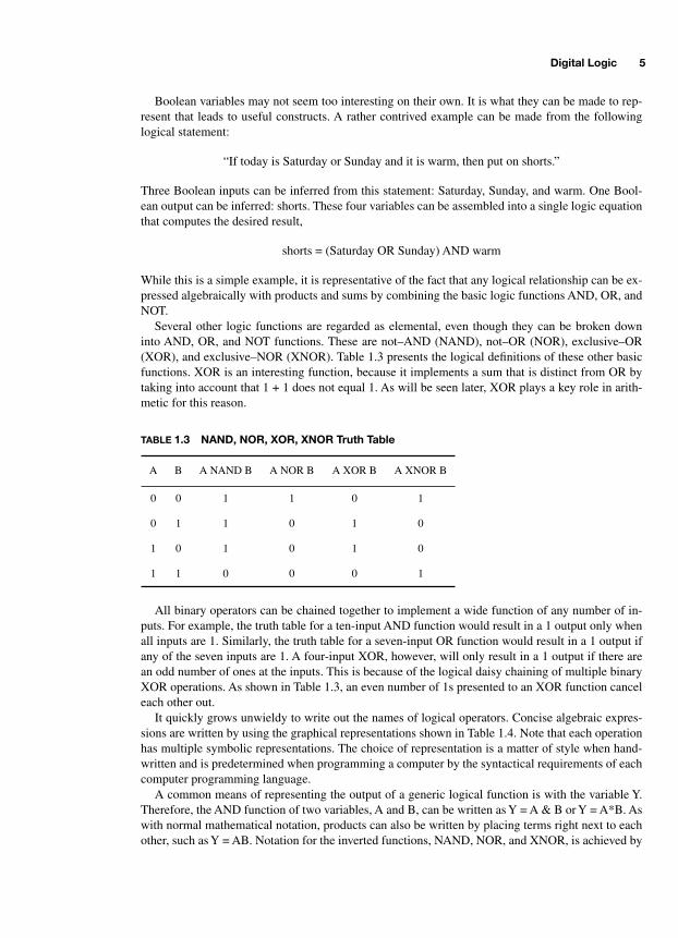
Several other logic functions are regarded as elemental, even though they can be broken downinto AND, OR, and NOT functions. These are not–AND (NAND), not–OR (NOR), exclusive–OR(XOR), and exclusive–NOR (XNOR). Table 1.3 presents the logical definitions of these other basicfunctions. XOR is an interesting function, because it implements a sum that is distinct from OR bytaking into account that 1 + 1 does not equal 1. As will be seen later, XOR plays a key role in arith-metic for this reason.
All binary operators can be chained together to implement a wide function of any number of in-puts. For example, the truth table for a ten-input AND function would result in a 1 output only whenall inputs are 1. Similarly, the truth table for a seven-input OR function would result in a 1 output ifany of the seven inputs are 1. A four-input XOR, however, will only result in a 1 output if there arean odd number of ones at the inputs. This is because of the logical daisy chaining of multiple binaryXOR operations. As shown in Table 1.3, an even number of 1s presented to an XOR function canceleach other out.
It quickly grows unwieldy to write out the names of logical operators. Concise algebraic expres-sions are written by using the graphical representations shown in Table 1.4. Note that each operationhas multiple symbolic representations. The choice of representation is a matter of style when hand-written and is predetermined when programming a computer by the syntactical requirements of eachcomputer programming language.
A common means of representing the output of a generic logical function is with the variable Y.Therefore, the AND function of two variables, A and B, can be written as Y = A & B or Y = A*B. Aswith normal mathematical notation, products can also be written by placing terms right next to eachother, such as Y = AB. Notation for the inverted functions, NAND, NOR, and XNOR, is achieved by
TABLE
1.3 NAND, NOR, XOR, XNOR Truth Table
A B A NAND B A NOR B A XOR B A XNOR B
0 0 1 1 0 1
0 1 1 0 1 0
1 0 1 0 1 0
1 1 0 0 0 1
-Balch.book Page 5 Thursday, May 15, 2003 3:46 PM
6 Digital Fundamentals
inverting the base function. Two equally valid ways of representing NAND are Y = A & B and Y =!(AB). Similarly, an XNOR might be written as Y = A
⊕
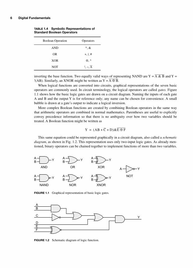
B.When logical functions are converted into circuits, graphical representations of the seven basic
operators are commonly used. In circuit terminology, the logical operators are called
gates
. Figure1.1 shows how the basic logic gates are drawn on a circuit diagram. Naming the inputs of each gateA and B and the output Y is for reference only; any name can be chosen for convenience. A smallbubble is drawn at a gate’s output to indicate a logical inversion.
More complex Boolean functions are created by combining Boolean operators in the same waythat arithmetic operators are combined in normal mathematics. Parentheses are useful to explicitlyconvey precedence information so that there is no ambiguity over how two variables should betreated. A Boolean function might be written as
This same equation could be represented graphically in a circuit diagram, also called a
schematicdiagram
, as shown in Fig. 1.2. This representation uses only two-input logic gates. As already men-tioned, binary operators can be chained together to implement functions of more than two variables.
TABLE
1.4 Symbolic Representations of Standard Boolean Operators
Boolean Operation Operators
AND *, &
OR +, |, #
XOR
⊕
, ^
NOT !, ~, A
AND OR XOR
NAND NOR XNOR
NOT
AB
YAB
YAB
Y
AB
YAB
YAB
Y
A Y
FIGURE 1.1 Graphical representation of basic logic gates.
Y AB C D+ +( )&E F⊕=
AB
C
DEF
Y
FIGURE 1.2 Schematic diagram of logic function.
-Balch.book Page 6 Thursday, May 15, 2003 3:46 PM

Digital Logic 7
An alternative graphical representation would use a three-input OR gate by collapsing the two-inputOR gates into a single entity.
1.2 BOOLEAN MANIPULATION
Boolean equations are invaluable when designing digital logic. To properly use and devise suchequations, it is helpful to understand certain basic rules that enable simplification and re-expressionof Boolean logic. Simplification is perhaps the most practical final result of Boolean manipulation,because it is easier and less expensive to build a circuit that does not contain unnecessary compo-nents. When a logical relationship is first set down on paper, it often is not in its most simplifiedform. Such a circuit will function but may be unnecessarily complex. Re-expression of a Booleanequation is a useful skill, because it can enable you to take better advantage of the logic resources atyour disposal instead of always having to use new components each time the logic is expanded orotherwise modified to function in a different manner. As will soon be shown, an OR gate can bemade to behave as an AND gate, and vice versa. Such knowledge can enable you to build a less-complex implementation of a Boolean equation.
First, it is useful to mention two basic identities:
A & A = 0 and A + A = 1
The first identity states that the product of any variable and its logical negation must always be false.It has already been shown that both operands of an AND function must be true for the result to betrue. Therefore, the first identity holds true, because it is impossible for both operands to be truewhen one is the negation of the other. The second identity states that the sum of any variable and itslogical negation must always be true. At least one operand of an OR function must be true for the re-sult to be true. As with the first identity, it is guaranteed that one operand will be true, and the otherwill be false.
Boolean algebra also has commutative, associative, and distributive properties as listed below:
•
Commutative: A & B = B & A and A + B = B + A
•
Associative: (A & B) & C = A & (B & C) and (A + B) + C = A + (B + C)
•
Distributive: A & (B + C) = A & B + A & C
The aforementioned identities, combined with these basic properties, can be used to simplify logic.For example,
A & B & C + A & B & C
can be re-expressed using the distributive property as
A & B & (C + C)
which we know by identity equals
A & B & (1) = A & B
Another useful identity, A + AB = A + B, can be illustrated using the truth table shown inTable 1.5.
-Balch.book Page 7 Thursday, May 15, 2003 3:46 PM
8 Digital Fundamentals
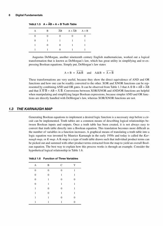
Augustus DeMorgan, another nineteenth century English mathematician, worked out a logicaltransformation that is known as DeMorgan’s law, which has great utility in simplifying and re-ex-pressing Boolean equations. Simply put, DeMorgan’s law states
and
These transformations are very useful, because they show the direct equivalence of AND and ORfunctions and how one can be readily converted to the other. XOR and XNOR functions can be rep-resented by combining AND and OR gates. It can be observed from Table 1.3 that A
⊕
B = AB + ABand that A
⊕ Β = ΑΒ + Α Β
. Conversions between XOR/XNOR and AND/OR functions are helpfulwhen manipulating and simplifying larger Boolean expressions, because simpler AND and OR func-tions are directly handled with DeMorgan’s law, whereas XOR/XNOR functions are not.
1.3 THE KARNAUGH MAP
Generating Boolean equations to implement a desired logic function is a necessary step before a cir-cuit can be implemented. Truth tables are a common means of describing logical relationships be-tween Boolean inputs and outputs. Once a truth table has been created, it is not always easy toconvert that truth table directly into a Boolean equation. This translation becomes more difficult asthe number of variables in a function increases. A graphical means of translating a truth table into alogic equation was invented by Maurice Karnaugh in the early 1950s and today is called the
Kar-naugh map
, or
K-map
. A K-map is a type of truth table drawn such that individual product terms canbe picked out and summed with other product terms extracted from the map to yield an overall Bool-ean equation. The best way to explain how this process works is through an example. Consider thehypothetical logical relationship in Table 1.6.
TABLE
1.5 A + AB = A + B Truth Table
A B AB A + AB A + B
0 0 0 0 0
0 1 1 1 1
1 0 0 1 1
1 1 0 1 1
TABLE
1.6 Function of Three Variables
A B C Y
0 0 0 1
0 0 1 1
0 1 0 0
0 1 1 1
1 0 0 1
1 0 1 1
1 1 0 0
1 1 1 0
A B+ A&B= A&B A B+=
-Balch.book Page 8 Thursday, May 15, 2003 3:46 PM
Digital Logic 9
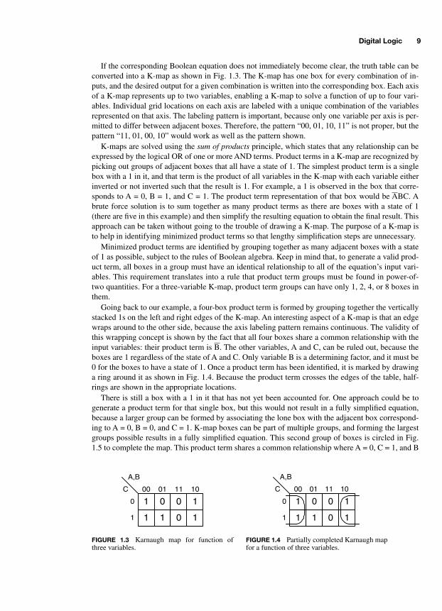
If the corresponding Boolean equation does not immediately become clear, the truth table can beconverted into a K-map as shown in Fig. 1.3. The K-map has one box for every combination of in-puts, and the desired output for a given combination is written into the corresponding box. Each axisof a K-map represents up to two variables, enabling a K-map to solve a function of up to four vari-ables. Individual grid locations on each axis are labeled with a unique combination of the variablesrepresented on that axis. The labeling pattern is important, because only one variable per axis is per-mitted to differ between adjacent boxes. Therefore, the pattern “00, 01, 10, 11” is not proper, but thepattern “11, 01, 00, 10” would work as well as the pattern shown.
K-maps are solved using the
sum of products
principle, which states that any relationship can beexpressed by the logical OR of one or more AND terms. Product terms in a K-map are recognized bypicking out groups of adjacent boxes that all have a state of 1. The simplest product term is a singlebox with a 1 in it, and that term is the product of all variables in the K-map with each variable eitherinverted or not inverted such that the result is 1. For example, a 1 is observed in the box that corre-sponds to A = 0, B = 1, and C = 1. The product term representation of that box would be ABC. Abrute force solution is to sum together as many product terms as there are boxes with a state of 1(there are five in this example) and then simplify the resulting equation to obtain the final result. Thisapproach can be taken without going to the trouble of drawing a K-map. The purpose of a K-map isto help in identifying minimized product terms so that lengthy simplification steps are unnecessary.
Minimized product terms are identified by grouping together as many adjacent boxes with a stateof 1 as possible, subject to the rules of Boolean algebra. Keep in mind that, to generate a valid prod-uct term, all boxes in a group must have an identical relationship to all of the equation’s input vari-ables. This requirement translates into a rule that product term groups must be found in power-of-two quantities. For a three-variable K-map, product term groups can have only 1, 2, 4, or 8 boxes inthem.
Going back to our example, a four-box product term is formed by grouping together the verticallystacked 1s on the left and right edges of the K-map. An interesting aspect of a K-map is that an edgewraps around to the other side, because the axis labeling pattern remains continuous. The validity ofthis wrapping concept is shown by the fact that all four boxes share a common relationship with theinput variables: their product term is B. The other variables, A and C, can be ruled out, because theboxes are 1 regardless of the state of A and C. Only variable B is a determining factor, and it must be0 for the boxes to have a state of 1. Once a product term has been identified, it is marked by drawinga ring around it as shown in Fig. 1.4. Because the product term crosses the edges of the table, half-rings are shown in the appropriate locations.
There is still a box with a 1 in it that has not yet been accounted for. One approach could be togenerate a product term for that single box, but this would not result in a fully simplified equation,because a larger group can be formed by associating the lone box with the adjacent box correspond-ing to A = 0, B = 0, and C = 1. K-map boxes can be part of multiple groups, and forming the largestgroups possible results in a fully simplified equation. This second group of boxes is circled in Fig.1.5 to complete the map. This product term shares a common relationship where A = 0, C = 1, and B
1
1
1
1
0
1
0
0
A,B
C
0
1
00 01 11 10
FIGURE 1.3 Karnaugh map for function ofthree variables.
C
1
1
1
1
0
1
0
0
A,B
0
1
00 01 11 10
FIGURE 1.4 Partially completed Karnaugh mapfor a function of three variables.
-Balch.book Page 9 Thursday, May 15, 2003 3:46 PM

10 Digital Fundamentals
is irrelevant: . It may appear tempting to create a product term consisting of the three boxes onthe bottom edge of the K-map. This is not valid because it does not result in all boxes sharing a com-mon product relationship, and therefore violates the power-of-two rule mentioned previously. Uponcompleting the K-map, all product terms are summed to yield a final and simplified Boolean equa-tion that relates the input variables and the output: .
Functions of four variables are just as easy to solve using a K-map. Beyond four variables, it ispreferable to break complex functions into smaller subfunctions and then combine the Booleanequations once they have been determined. Figure 1.6 shows an example of a completed Karnaughmap for a hypothetical function of four variables. Note the overlap between several groups toachieve a simplified set of product terms. The lager a group is, the fewer unique terms will be re-quired to represent its logic. There is nothing to lose and something to gain by forming a largergroup whenever possible. This K-map has four product terms that are summed for a final result:
.In both preceding examples, each result box in the truth table and Karnaugh map had a clearly de-
fined state. Some logical relationships, however, do not require that every possible result necessarilybe a one or a zero. For example, out of 16 possible results from the combination of four variables,only 14 results may be mandated by the application. This may sound odd, but one explanation couldbe that the particular application simply cannot provide the full 16 combinations of inputs. The spe-cific reasons for this are as numerous as the many different applications that exist. In such circum-stances these so-called
don’t care
results can be used to reduce the complexity of your logic.Because the application does not care what result is generated for these few combinations, you canarbitrarily set the results to 0s or 1s so that the logic is minimized. Figure 1.7 is an example thatmodifies the Karnaugh map in Fig. 1.6 such that two don’t care boxes are present. Don’t care valuesare most commonly represented with “x” characters. The presence of one x enables simplification ofthe resulting logic by converting it to a 1 and grouping it with an adjacent 1. The other x is set to 0 sothat it does not waste additional logic terms. The new Boolean equation is simplified by removing Bfrom the last term, yielding . It is helpful to remember that x val-ues can generally work to your benefit, because their presence imposes fewer requirements on thelogic that you must create to get the job done.
1.4 BINARY AND HEXADECIMAL NUMBERING
The fact that there are only two valid Boolean values, 1 and 0, makes the
binary
numbering systemappropriate for logical expression and, therefore, for digital systems. Binary is a base-2 system in
AC
1
1
1
1
0
1
0
0
A,B
0
1
00 01 11 10
FIGURE 1.5 Completed Karnaugh map for afunction of three variables.
1
1
1
1
1
1
0
0
A,B
C,D
00
01
00 01 11 10
0
0
0
0
0
1
1
0
11
10
FIGURE 1.6 Completed Karnaugh map forfunction of four variables.
Y B AC+=
Y A C B C ABD ABCD+ + +=
Y A C B C ABD ACD+ + +=
-Balch.book Page 10 Thursday, May 15, 2003 3:46 PM

Digital Logic 11
which only the digits 1 and 0 exist. Binary follows the same laws of mathematics as decimal, orbase-10, numbering. In decimal, the number 191 is understood to mean one hundreds plus nine tensplus one ones. It has this meaning, because each digit represents a successively higher power of tenas it moves farther left of the decimal point. Representing 191 in mathematical terms to illustratethese increasing powers of ten can be done as follows:
191 = 1
×
10
2
+ 9
×
10
1
+ 1
×
10
0
Binary follows the same rule, but instead of powers of ten, it works on powers of two. The num-ber 110 in binary (written as 110
2
to explicitly denote base 2) does not equal 110
10
(decimal).Rather, 110
2
= 1
×
2
2
+ 1
×
2
1
+ 0
×
2
0
= 6
10
. The number 191
10
can be converted to binary by per-forming successive division by decreasing powers of 2 as shown below:
191 ÷ 2
7
= 191 ÷ 128 = 1 remainder 63
63 ÷ 2
6
= 63 ÷ 64 = 0 remainder 63
63 ÷ 2
5
= 63 ÷ 32 = 1 remainder 31
31 ÷ 2
4
= 31 ÷ 16 = 1 remainder 15
15 ÷ 2
3
= 15 ÷ 8 = 1 remainder 7
7 ÷ 2
2
= 7 ÷ 4 = 1 remainder 3
3 ÷ 2
1
= 3 ÷ 2 = 1 remainder 1
1 ÷ 2
0
= 1 ÷ 1 = 1 remainder 0
The final result is that 191
10
= 10111111
2
. Each binary digit is referred to as a
bit
. A group of Nbits can represent decimal numbers from 0 to 2
N
– 1. There are eight bits in a
byte
, more formallycalled an
octet
in certain circles, enabling a byte to represent numbers up to 2
8
– 1 = 255. The pre-ceding example shows the eight power-of-two terms in a byte. If each term, or bit, has its maximumvalue of 1, the result is 128 + 64 + 32 + 16 + 8 + 4 + 2 + 1 = 255.
While binary notation directly represents digital logic states, it is rather cumbersome to workwith, because one quickly ends up with long strings of ones and zeroes.
Hexadecimal
, or base 16(
hex
for short), is a convenient means of representing binary numbers in a more succinct notation.Hex matches up very well with binary, because one hex digit represents four binary digits, given that
1
1
1
1
1
1
0
0
A,B
C,D
00
01
00 01 11 10
x
0
x
0
0
1
1
0
11
10
FIGURE 1.7 Karnaugh map for function of four vari-ables with two “don’t care” values.
-Balch.book Page 11 Thursday, May 15, 2003 3:46 PM
12 Digital Fundamentals
2
4
= 16. A four-bit group is called a
nibble
. Because hex requires 16 digits, the letters “A” through“F” are borrowed for use as hex digits beyond 9. The 16 hex digits are defined in Table 1.7.
The preceding example, 191
10
= 10111111
2
, can be converted to hex easily by grouping the eightbits into two nibbles and representing each nibble with a single hex digit:
1011
2
= (8 + 2 + 1)
10
= 11
10
= B
16
1111
2
= (8 + 4 + 2 + 1)
10
= 15
10
= F
16
Therefore, 191
10
= 10111111
2
= BF
16
. There are two common prefixes, 0x and $, and a commonsuffix, h, that indicate hex numbers. These styles are used as follows: BF
16
= 0xBF = $BF = BFh. Allthree are used by engineers, because they are more convenient than appending a subscript “16” toeach number in a document or computer program. Choosing one style over another is a matter ofpreference.
Whether a number is written using binary or hex notation, it remains a string of bits, each ofwhich is 1 or 0. Binary numbering allows arbitrary data processing algorithms to be reduced toBoolean equations and implemented with logic gates. Consider the equality comparison of two four-bit numbers, M and N.
“If M = N, then the equality test is true.”
Implementing this function in gates first requires a means of representing the individual bits thatcompose M and N. When a group of bits are used to represent a common entity, the bits are num-bered in ascending or descending order with zero usually being the smallest index. The bit that rep-resents 2
0
is termed the
least-significant bit
, or LSB, and the bit that represents the highest power oftwo in the group is called the
most-significant bit
, or MSB. A four-bit quantity would have the MSBrepresent 2
3
. M and N can be ordered such that the MSB is bit number 3, and the LSB is bit number0. Collectively, M and N may be represented as M[3:0] and N[3:0] to denote that each contains fourbits with indices from 0 to 3. This presentation style allows any arbitrary bit of M or N to beuniquely identified with its index.
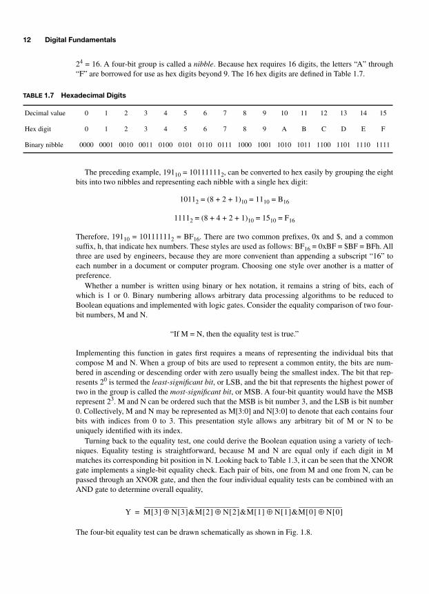
Turning back to the equality test, one could derive the Boolean equation using a variety of tech-niques. Equality testing is straightforward, because M and N are equal only if each digit in Mmatches its corresponding bit position in N. Looking back to Table 1.3, it can be seen that the XNORgate implements a single-bit equality check. Each pair of bits, one from M and one from N, can bepassed through an XNOR gate, and then the four individual equality tests can be combined with anAND gate to determine overall equality,
The four-bit equality test can be drawn schematically as shown in Fig. 1.8.
TABLE
1.7 Hexadecimal Digits
Decimal value 0 1 2 3 4 5 6 7 8 9 10 11 12 13 14 15
Hex digit 0 1 2 3 4 5 6 7 8 9 A B C D E F
Binary nibble 0000 0001 0010 0011 0100 0101 0110 0111 1000 1001 1010 1011 1100 1101 1110 1111
Y M 3[ ] N 3[ ]⊕ &M 2[ ] N 2[ ]⊕ &M 1[ ] N 1[ ]⊕ &M 0[ ] N 0[ ]⊕=
-Balch.book Page 12 Thursday, May 15, 2003 3:46 PM
Digital Logic 13
Logic to compare one number against a constant is simpler than comparing two numbers, becausethe number of inputs to the Boolean equation is cut in half. If, for example, one wanted to compareM[3:0] to a constant 10012 (910), the logic would reduce to just a four-input AND gate with two in-verted inputs:
When working with computers and other digital systems, numbers are almost always written inhex notation simply because it is far easier to work with fewer digits. In a 32-bit computer, a valuecan be written as either 8 hex digits or 32 bits. The computer’s logic always operates on raw binaryquantities, but people generally find it easier to work in hex. An interesting historical note is that hexwas not always the common method of choice for representing bits. In the early days of computing,through the 1960s and 1970s, octal (base-8) was used predominantly. Instead of a single hex digitrepresenting four bits, a single octal digit represents three bits, because 23 = 8. In octal, 19110 =2778. Whereas bytes are the lingua franca of modern computing, groups of two or three octal digitswere common in earlier times.
Because of the inherent binary nature of digital systems, quantities are most often expressed in or-ders of magnitude that are tied to binary rather than decimal numbering. For example, a “round num-ber” of bytes would be 1,024 (210) rather than 1000 (103). Succinct terminology in reference toquantities of data is enabled by a set of standard prefixes used to denote order of magnitude. Further-more, there is a convention of using a capital B to represent a quantity of bytes and using a lower-case b to represent a quantity of bits. Commonly observed prefixes used to quantify sets of data arelisted in Table 1.8. Many memory chips and communications interfaces are expressed in units ofbits. One must be careful not to misunderstand a specification. If you need to store 32 MB of data, besure to use a 256 Mb memory chip rather than a 32 Mb device!
TABLE 1.8 Common Binary Magnitude Prefixes
Prefix Definition Order of Magnitude Abbreviation Usage
Kilo (1,024)1 = 1,024 210 k kB
Mega (1,024)2 = 1,048,576 220 M MB
Giga (1,024)3 = 1,073,741,824 230 G GB
Tera (1,024)4 = 1,099,511,627,776 240 T TB
Peta (1,024)5 = 1,125,899,906,842,624 250 P PB
Exa (1,024)6 = 1,152,921,504,606,846,976 260 E EB
M[3]N[3]
M[2]N[2]
M[1]N[1]
M[0]N[0]
Y
FIGURE 1.8 Four-bit equality logic.
y M 3[ ]&M 2[ ]&M 1[ ]&M 0[ ]=
-Balch.book Page 13 Thursday, May 15, 2003 3:46 PM

14 Digital Fundamentals
The majority of digital components adhere to power-of-two magnitude definitions. However,some industries break from these conventions largely for reasons of product promotion. A key exam-ple is the hard disk drive industry, which specifies prefixes in decimal terms (e.g., 1 MB = 1,000,000bytes). The advantage of doing this is to inflate the apparent capacity of the disk drive: a drive thatprovides 10,000,000,000 bytes of storage can be labeled as “10 GB” in decimal terms, but it wouldhave to be labeled as only 9.31 GB in binary terms (1010 ÷ 230 = 9.31).
1.5 BINARY ADDITION
Despite the fact that most engineers use hex data representation, it has already been shown that logicgates operate on strings of bits that compose each unit of data. Binary arithmetic is performed ac-cording to the same rules as decimal arithmetic. When adding two numbers, each column of digits isadded in sequence from right to left and, if the sum of any column is greater than the value of thehighest digit, a carry is added to the next column. In binary, the largest digit is 1, so any sum greaterthan 1 will result in a carry. The addition of 1112 and 0112 (7 + 3 = 10) is illustrated below.
In the first column, the sum of two ones is 210, or 102, resulting in a carry to the second column.The sum of the second column is 310, or 112, resulting in both a carry to the next column and a onein the sum. When all three columns are completed, a carry remains, having been pushed into a newfourth column. The carry is, in effect, added to leading 0s and descends to the sum line as a 1.
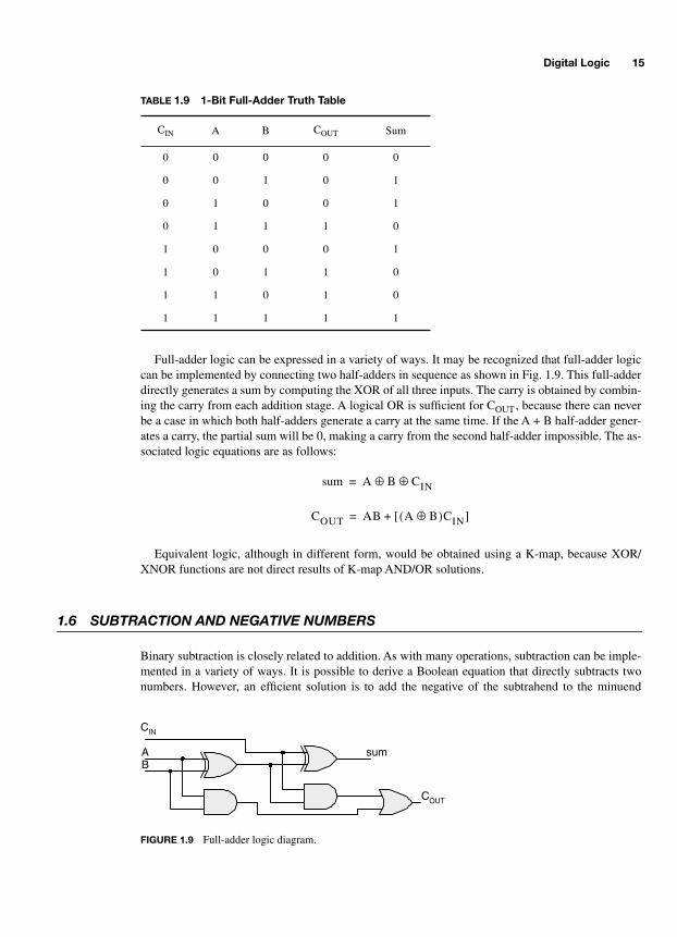
The logic to perform binary addition is actually not very complicated. At the heart of a 1-bit adderis the XOR gate, whose result is the sum of two bits without the associated carry bit. An XOR gategenerates a 1 when either input is 1, but not both. On its own, the XOR gate properly adds 0 + 0, 0 +1, and 1 + 0. The fourth possibility, 1 + 1 = 2, requires a carry bit, because 210 = 102. Given that acarry is generated only when both inputs are 1, an AND gate can be used to produce the carry. A so-called half-adder is represented as follows:
This logic is called a half-adder because it does only part of the job when multiple bits must beadded together. Summing multibit data values requires a carry to ripple across the bit positions start-ing from the LSB. The half-adder has no provision for a carry input from the preceding bit position.A full-adder incorporates a carry input and can therefore be used to implement a complete summa-tion circuit for an arbitrarily large pair of numbers. Table 1.9 lists the complete full-adder input/out-put relationship with a carry input (CIN) from the previous bit position and a carry output (COUT) tothe next bit position. Note that all possible sums from zero to three are properly accounted for bycombining COUT and sum. When CIN = 0, the circuit behaves exactly like the half-adder.
1 1 1 0 carry bits
1 1 1
+ 0 1 1
1 0 1 0
sum A B⊕=
carry AB=
-Balch.book Page 14 Thursday, May 15, 2003 3:46 PM
Digital Logic 15
Full-adder logic can be expressed in a variety of ways. It may be recognized that full-adder logiccan be implemented by connecting two half-adders in sequence as shown in Fig. 1.9. This full-adderdirectly generates a sum by computing the XOR of all three inputs. The carry is obtained by combin-ing the carry from each addition stage. A logical OR is sufficient for COUT, because there can neverbe a case in which both half-adders generate a carry at the same time. If the A + B half-adder gener-ates a carry, the partial sum will be 0, making a carry from the second half-adder impossible. The as-sociated logic equations are as follows:
Equivalent logic, although in different form, would be obtained using a K-map, because XOR/XNOR functions are not direct results of K-map AND/OR solutions.
1.6 SUBTRACTION AND NEGATIVE NUMBERS
Binary subtraction is closely related to addition. As with many operations, subtraction can be imple-mented in a variety of ways. It is possible to derive a Boolean equation that directly subtracts twonumbers. However, an efficient solution is to add the negative of the subtrahend to the minuend
TABLE 1.9 1-Bit Full-Adder Truth Table
CIN A B COUT Sum
0 0 0 0 0
0 0 1 0 1
0 1 0 0 1
0 1 1 1 0
1 0 0 0 1
1 0 1 1 0
1 1 0 1 0
1 1 1 1 1
AB
CIN
sum
COUT
FIGURE 1.9 Full-adder logic diagram.
sum A B CIN⊕ ⊕=
COUT AB A B⊕( )CIN[ ]+=
-Balch.book Page 15 Thursday, May 15, 2003 3:46 PM

16 Digital Fundamentals
rather than directly subtracting the subtrahend from the minuend. These are, of course, identical op-erations: A – B = A + (–B). This type of arithmetic is referred to as subtraction by addition of thetwo’s complement. The two’s complement is the negative representation of a number that allows theidentity A – B = A + (–B) to hold true.
Subtraction requires a means of expressing negative numbers. To this end, the most-significantbit, or left-most bit, of a binary number is used as the sign-bit when dealing with signed numbers. Anegative number is indicated when the sign-bit equals 1. Unsigned arithmetic does not involve asign-bit, and therefore can express larger absolute numbers, because the MSB is merely an extradigit rather than a sign indicator.
The first step in performing two’s complement subtraction is to convert the subtrahend into a neg-ative equivalent. This conversion is a two-step process. First, the binary number is inverted to yield aone’s complement. Then, 1 is added to the one’s complement version to yield the desired two’s com-plement number. This is illustrated below:
Observe that the unsigned four-bit number that can represent values from 0 to 1510 now representssigned values from –8 to 7. The range about zero is asymmetrical because of the sign-bit and the factthat there is no negative 0. Once the two’s complement has been obtained, subtraction is performedby adding the two’s complement subtrahend to the minuend. For example, 7 – 5 = 2 would be per-formed as follows, given the –5 representation obtained above:
Note that the final carry-bit past the sign-bit is ignored. An example of subtraction with a negativeresult is 3 – 5 = –2.
Here, the result has its sign-bit set, indicating a negative quantity. We can check the answer by calcu-lating the two’s complement of the negative quantity.
0 1 0 1 Original number (5)
1 0 1 0 One’s complement
+ 0 0 0 1 Add one
1 0 1 1 Two’s complement (–5)
1 1 1 1 0 Carry bits
0 1 1 1 Minuend (7)
+ 1 0 1 1 “Subtrahend” (–5)
0 0 1 0 Result (2)
1 1 0 Carry bits
0 0 1 1 Minuend (3)
+ 1 0 1 1 “Subtrahend” (–5)
1 1 1 0 Result (–2)
-Balch.book Page 16 Thursday, May 15, 2003 3:46 PM

Digital Logic 17
This check succeeds and shows that two’s complement conversions work “both ways,” going backand forth between negative and positive numbers. The exception to this rule is the asymmetrical casein which the largest negative number is one more than the largest positive number as a result of thepresence of the sign-bit. A four-bit number, therefore, has no positive counterpart of –8. Similarly, an8-bit number has no positive counterpart of –128.
1.7 MULTIPLICATION AND DIVISION
Multiplication and division follow the same mathematical rules used in decimal numbering. How-ever, their implementation is substantially more complex as compared to addition and subtraction.Multiplication can be performed inside a computer in the same way that a person does so on paper.Consider 12 × 12 = 144.
The multiplication process grows in steps as the number of digits in each multiplicand increases,because the number of partial products increases. Binary numbers function the same way, but thereeasily can be many partial products, because numbers require more digits to represent them in binaryversus decimal. Here is the same multiplication expressed in binary (1100 × 1100 = 10010000):
1 1 1 0 Original number (–2)
0 0 0 1 One’s complement
+ 0 0 0 1 Add one
0 0 1 0 Two’s complement (2)
1 2
X 1 2
2 4 Partial product × 100
+ 1 2 Partial product × 101
1 4 4 Final product
1 1 0 0
X 1 1 0 0
0 0 0 0 Partial product × 20
0 0 0 0 Partial product × 21
1 1 0 0 Partial product × 22
+ 1 1 0 0 Partial product × 23
1 0 0 1 0 0 0 0 Final product
-Balch.book Page 17 Thursday, May 15, 2003 3:46 PM
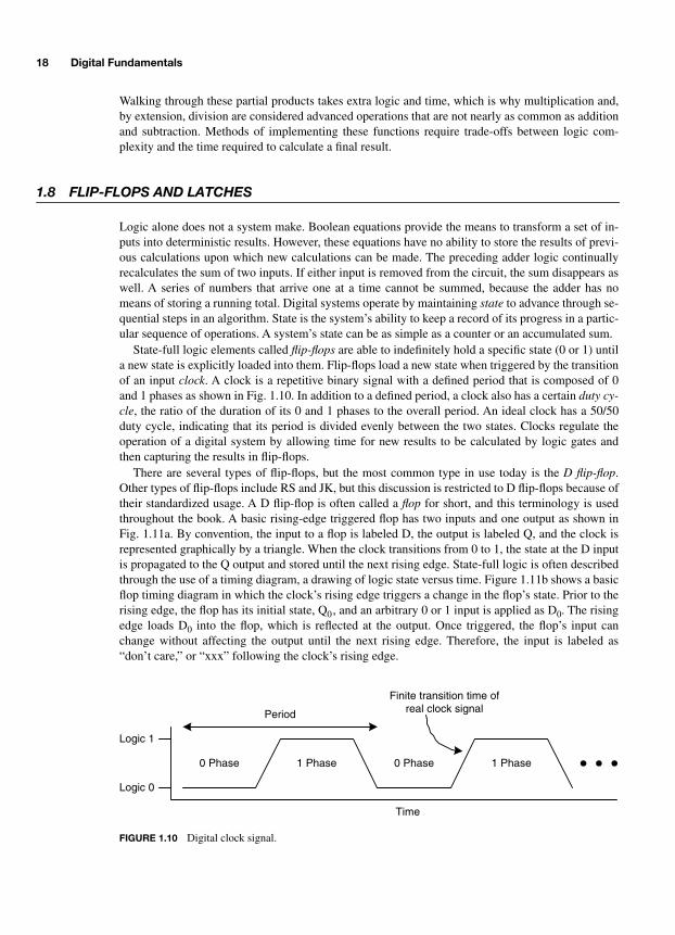
18 Digital Fundamentals
Walking through these partial products takes extra logic and time, which is why multiplication and,by extension, division are considered advanced operations that are not nearly as common as additionand subtraction. Methods of implementing these functions require trade-offs between logic com-plexity and the time required to calculate a final result.
1.8 FLIP-FLOPS AND LATCHES
Logic alone does not a system make. Boolean equations provide the means to transform a set of in-puts into deterministic results. However, these equations have no ability to store the results of previ-ous calculations upon which new calculations can be made. The preceding adder logic continuallyrecalculates the sum of two inputs. If either input is removed from the circuit, the sum disappears aswell. A series of numbers that arrive one at a time cannot be summed, because the adder has nomeans of storing a running total. Digital systems operate by maintaining state to advance through se-quential steps in an algorithm. State is the system’s ability to keep a record of its progress in a partic-ular sequence of operations. A system’s state can be as simple as a counter or an accumulated sum.
State-full logic elements called flip-flops are able to indefinitely hold a specific state (0 or 1) untila new state is explicitly loaded into them. Flip-flops load a new state when triggered by the transitionof an input clock. A clock is a repetitive binary signal with a defined period that is composed of 0and 1 phases as shown in Fig. 1.10. In addition to a defined period, a clock also has a certain duty cy-cle, the ratio of the duration of its 0 and 1 phases to the overall period. An ideal clock has a 50/50duty cycle, indicating that its period is divided evenly between the two states. Clocks regulate theoperation of a digital system by allowing time for new results to be calculated by logic gates andthen capturing the results in flip-flops.
There are several types of flip-flops, but the most common type in use today is the D flip-flop.Other types of flip-flops include RS and JK, but this discussion is restricted to D flip-flops because oftheir standardized usage. A D flip-flop is often called a flop for short, and this terminology is usedthroughout the book. A basic rising-edge triggered flop has two inputs and one output as shown inFig. 1.11a. By convention, the input to a flop is labeled D, the output is labeled Q, and the clock isrepresented graphically by a triangle. When the clock transitions from 0 to 1, the state at the D inputis propagated to the Q output and stored until the next rising edge. State-full logic is often describedthrough the use of a timing diagram, a drawing of logic state versus time. Figure 1.11b shows a basicflop timing diagram in which the clock’s rising edge triggers a change in the flop’s state. Prior to therising edge, the flop has its initial state, Q0, and an arbitrary 0 or 1 input is applied as D0. The risingedge loads D0 into the flop, which is reflected at the output. Once triggered, the flop’s input canchange without affecting the output until the next rising edge. Therefore, the input is labeled as“don’t care,” or “xxx” following the clock’s rising edge.
Logic 1
Logic 0
Time
0 Phase 1 Phase 0 Phase 1 Phase
Period
Finite transition time ofreal clock signal
FIGURE 1.10 Digital clock signal.
-Balch.book Page 18 Thursday, May 15, 2003 3:46 PM

Digital Logic 19
Rising-edge flops are the norm, although some flops are falling-edge triggered. A falling-edgetriggered flop is indicated by placing an inversion bubble at the clock input as shown in Fig. 1.12.Operation is the same, with the exception that the polarity of the clock is inverted. The remainder ofthis discussion assumes rising-edge triggered flops unless explicitly stated otherwise.
There are several common feature enhancements to the basic flop, including clock-enable, set,and clear inputs and a complementary output. Clock enable is used as a triggering qualifier eachtime a rising clock edge is detected. The D input is loaded only if clock enable is set to its activestate. Inputs in general are defined by device manufacturers to be either active-low or active-high. Anactive-low signal is effective when set to 0, and an active-high signal is effective when set to 1. Sig-nals are assumed to be active-high unless otherwise indicated. Active-low inputs are commonly indi-cated by the same inversion bubble used to indicate a falling-edge clock. When a signal is driven toits active state, it is said to be asserted. A signal is de-asserted when driven to its inactive state. Setand clear inputs explicitly force a flop to a 1 or 0 state, respectively. Such inputs are often used to ini-tialize a digital system to a known state when it is first turned on. Otherwise, the flop powers up in arandom state, which can cause problems for certain logic. Set and clear inputs can be either synchro-nous or asynchronous. Synchronous inputs take effect only on the rising clock edge, while asynchro-nous inputs take effect immediately upon being asserted. A complementary output is simply aninverted copy of the main output.
A truth table for a flop enhanced with the features just discussed is shown in Table 1.10. The truthtable assumes a synchronous, active-high clock enable (EN) and synchronous, active-low set andclear inputs. The rising edge of the clock is indicated by the ↑ symbol. When the clock is at eitherstatic value, the outputs of the flop remain in their existing states. When the clock rises, the D, EN,
, and inputs are sampled and acted on accordingly. As a general rule, conflicting infor-mation such as asserting and at the same time should be avoided, because unknown re-sults may arise. The exact behavior in this case depends on the specific flop implementation and mayvary by manufacturer.
A basic application of flops is a binary ripple counter. Multiple flops can be cascaded as shown inFig. 1.13 such that each complementary output is fed back to that flop’s input and also used to clockthe next flop. The current count value is represented by the noninverted flop outputs with the firstflop representing the LSB. A three-bit counter is shown with an active-low reset input so that thecounter can be cleared to begin at zero. The counter circuit diagram uses the standard convention of
D Q
(a)
Clock
D
Q
xxxInitial Value = D0
Initial Value = Q0 New Value = D0
(b)
FIGURE 1.11 Rising-edge triggered flop.
(a) (b)
D Q Clock
D
Q
xxxInitial Value = D0
Initial Value = Q0 New Value = D0
FIGURE 1.12 Falling-edge triggered flop.
CLR SETCLR SET
-Balch.book Page 19 Thursday, May 15, 2003 3:46 PM

20 Digital Fundamentals
showing electrical connectivity between intersecting wires by means of a junction dot. Wires thatcross without a dot at their intersection are not electrically connected.
The ripple counter’s operation is illustrated in Fig. 1.14. Each bit starts out at zero if RESET is as-serted. Counting begins on the first rising edge of CLK following the de-assertion of RESET. TheLSB, Q[0], increments from 0 to 1, because its D input is driven by the complementary output,which is 1. The complementary output transitions to 0, which does not trigger the Q[1] rising-edgeflop, but IT does set up the conditions for a trigger after the next CLK rising edge. When CLK risesagain, Q[0] transitions back to 0, and Q[0] transitions to 1, forming a rising edge to trigger Q[1],which loads a 1. This sequence continues until the count value reaches 7, at which point the counterrolls over to zero, and the sequence begins again.
An undesirable characteristic of the ripple counter is that it takes longer for a new count value tostabilize as the number of bits in the counter increases. Because each flop’s output clocks the nextflop in the sequence, it can take some time for all flops to be updated following the CLK rising edge.Slow systems may not find this burdensome, but the added ripple delay is unacceptable in most high-speed applications. Ways around this problem will be discussed shortly.
TABLE 1.10 Enhanced Flop Truth Table
Clock D EN CLR SET Q Q
0 X X X X Qstat ic
↑ 0 0 1 1 Qstat ic
↑ 0 1 1 1 0 1
↑ 1 1 1 1 1 0
↑ X X 0 1 0 1
↑ X X 1 0 1 0
↑ X X 0 0 ? ?
1 X X X X Qstat ic
D
Q
CLR
Q D
Q
CLR
Q D
Q
CLR
Q
RESET
CLK
Q[0] Q[1] Q[2]
FIGURE 1.13 Three-bit ripple counter.
Qstatic
Qstatic
Qstatic
-Balch.book Page 20 Thursday, May 15, 2003 3:46 PM

Digital Logic 21
A relative of the flop is the D-type latch, which is also capable of retaining its state indefinitely. Alatch has a D input, a Q output, and an enable (EN) signal. Whereas a flop transfers its input to itsoutput only on the active clock edge, a latch continuously transfers D to Q while EN is active.Latches are level sensitive, whereas flops are edge sensitive. A latch retains its state while EN is in-active. Table 1.11 shows the latch’s truth table. Latches are simpler than flops and are unsuited tomany applications in which flops are used. Latches would not substitute for flops in the precedingripple counter example because, while the enable input is high, a continuous loop would be formedbetween the complementary output and input. This would result in rapid, uncontrolled oscillation ateach latch during the time that the enable is held high.
Latches are available as discrete logic elements and can also be assembled from simpler logicgates. The Boolean equation for a latch requires feeding back the output as follows:
When EN is high, D is passed to Q. Q then feeds back to the second AND function, which maintainsthe state when EN is low. Latches are used in designs based on older technology that was conceivedwhen the latch’s simplicity yielded a cost savings or performance advantage. Most state-full ele-ments today are flops unless there is a specific benefit to using a latch.
1.9 SYNCHRONOUS LOGIC
It has been shown that clock signals regulate the operation of a state-full digital system by causingnew values to be loaded into flops on each active clock edge. Synchronous logic is the general term
TABLE 1.11 D-Latch Truth Table
EN D Q
0 X Q0
1 0 0
1 1 1
CLK
Q[0]
0
RESET
Q[1]
Q[2]
Count: Q[2:0] 1 2 3 4 5 6 7 0
FIGURE 1.14 Ripple counter timing diagram.
Q EN&D( ) EN&Q( )+=
-Balch.book Page 21 Thursday, May 15, 2003 3:46 PM
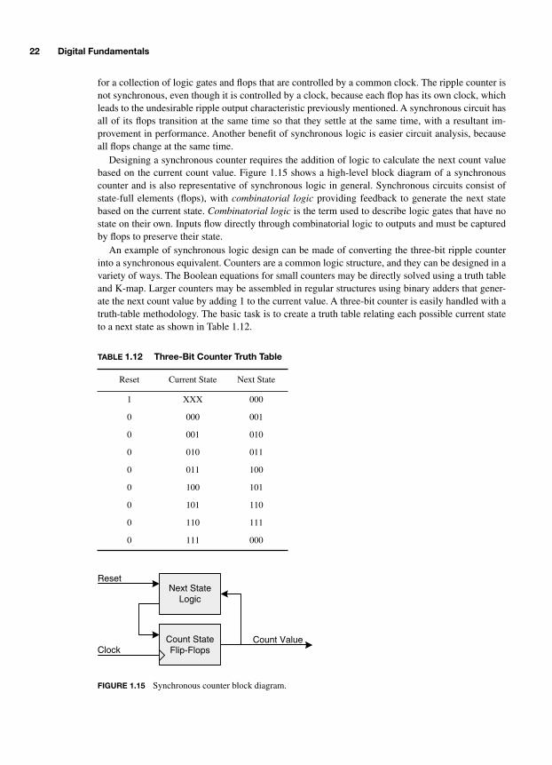
22 Digital Fundamentals
for a collection of logic gates and flops that are controlled by a common clock. The ripple counter isnot synchronous, even though it is controlled by a clock, because each flop has its own clock, whichleads to the undesirable ripple output characteristic previously mentioned. A synchronous circuit hasall of its flops transition at the same time so that they settle at the same time, with a resultant im-provement in performance. Another benefit of synchronous logic is easier circuit analysis, becauseall flops change at the same time.
Designing a synchronous counter requires the addition of logic to calculate the next count valuebased on the current count value. Figure 1.15 shows a high-level block diagram of a synchronouscounter and is also representative of synchronous logic in general. Synchronous circuits consist ofstate-full elements (flops), with combinatorial logic providing feedback to generate the next statebased on the current state. Combinatorial logic is the term used to describe logic gates that have nostate on their own. Inputs flow directly through combinatorial logic to outputs and must be capturedby flops to preserve their state.
An example of synchronous logic design can be made of converting the three-bit ripple counterinto a synchronous equivalent. Counters are a common logic structure, and they can be designed in avariety of ways. The Boolean equations for small counters may be directly solved using a truth tableand K-map. Larger counters may be assembled in regular structures using binary adders that gener-ate the next count value by adding 1 to the current value. A three-bit counter is easily handled with atruth-table methodology. The basic task is to create a truth table relating each possible current stateto a next state as shown in Table 1.12.
TABLE 1.12 Three-Bit Counter Truth Table
Reset Current State Next State
1 XXX 000
0 000 001
0 001 010
0 010 011
0 011 100
0 100 101
0 101 110
0 110 111
0 111 000
Next StateLogic
Count StateFlip-Flops
Count Value
Reset
Clock
FIGURE 1.15 Synchronous counter block diagram.
-Balch.book Page 22 Thursday, May 15, 2003 3:46 PM

Digital Logic 23
Three Boolean equations are necessary, one for each bit that feeds back to the count state flops. Ifthe flop inputs are labeled D[2:0], the outputs are labeled Q[2:0], and an active-high synchronous re-set is defined, the following equations can be developed:
Each equation’s output is forced to 0 when RESET is asserted. Otherwise, the counter increments oneach rising clock edge. Synchronous logic design allows any function to be implemented by chang-ing the feedback logic. It would not be difficult to change the counter logic to count only odd or evennumbers, or to count only as high as 5 before rolling over to 0. Unlike the ripple counter, whosestructure supports a fixed counting sequence, next state logic can be defined arbitrarily according toan application’s needs.
1.10 SYNCHRONOUS TIMING ANALYSIS
Logic elements, including flip-flops and gates, are physical devices that have finite response times tostimuli. Each of these elements exhibits a certain propagation delay between the time that an input ispresented and the time that an output is generated. As more gates are chained together to create morecomplex logic functions, the overall propagation delay of signals between the end points increases.Flip-flops are triggered by the rising edge of a clock to load their new state, requiring that the inputto the flip-flop is stable prior to the rising edge. Similarly, a flip-flop’s output stabilizes at a new statesome time after the rising edge. In between the output of a flip-flop and the input of another flip-flopis an arbitrary collection of logic gates, as seen in the preceding synchronous counter circuit. Syn-chronous timing analysis is the study of how the various delays in a synchronous circuit combine tolimit the speed at which that circuit can operate. As might be expected, circuits with lesser delays areable to run faster.
A clock breaks time into discrete intervals that are each the duration of a single clock period.From a timing analysis perspective, each clock period is identical to the last, because each risingclock edge is a new flop triggering event. Therefore, timing analysis considers a circuit’s delays overone clock period, between successive rising (or falling) clock edges. Knowing that a wide range ofclock frequencies can be applied to a circuit, the question of time arises of how fast the clock can gobefore the circuit stops working reliably. The answer is that the clock must be slow enough to allowsufficient time for the output of a flop to stabilize, for the signal to propagate through the combinato-rial logic gates, and for the input of the destination flop to stabilize. The clock must also be slowenough for the flop to reliably detect each edge. Each flop circuit is characterized by a minimumclock pulse width that must be met. Failing to meet this minimum time can result in the flop missingclock events.
Timing analysis revolves around the basic timing parameters of a flop: input setup time (tSU), in-put hold time (tH), and clock-to-out time (tCO). Setup time specifies the time immediately precedingthe rising edge of the clock by which the input must be stable. If the input changes too soon beforethe clock edge, the electrical circuitry within the flop will not have enough time to properly recog-nize the state of the input. Hold time places a restriction on how soon after the clock edge the input
D 0[ ] Q 0[ ]&RESET=
D 1[ ] Q 0[ ]&Q 1[ ]( ) Q 0[ ]&Q 1[ ]( )+ &RESET Q 0[ ] Q 1[ ]⊕( )&RESET= =
D 2[ ] Q 2[ ]&Q 1[ ]&Q 0[ ]( ) Q 2[ ]&Q 1[ ]( ) Q 2[ ]&Q 0[ ]( )+ + &RESET=
-Balch.book Page 23 Thursday, May 15, 2003 3:46 PM

24 Digital Fundamentals
may begin to change. Again, if the input changes too soon after the clock edge, it may not be prop-erly detected by the circuitry. Clock-to-out time specifies how soon after the clock edge the outputwill be updated to the state presented at the input. These parameters are very brief in duration andare usually measured in nanoseconds. One nanosecond, abbreviated “ns,” is one billionth of a sec-ond. In very fast microchips, they may be measured in picoseconds, or one trillionth or a second.
Consistent terminology is necessary when conducting timing analysis. Timing is expressed inunits of both clock frequency and time. Clock frequency, or speed, is quantified in units of hertz,named after the twentieth century German physicist, Gustav Hertz. One hertz is equivalent to oneclock cycle per second—one transition from low to high and a second transition from high to low.Units of hertz are abbreviated as Hz and are commonly accompanied by prefixes that denote an or-der of magnitude. Commonly observed prefixes used to quantify clock frequency and their defini-tions are listed in Table 1.13. Unlike quantities of bytes that use binary-based units, clock frequencyuses decimal-based units.
Units of time are used to express a clock’s period as well as basic logic element delays such asthe aforementioned tSU, tH, and tCO. As with frequency, standard prefixes are used to indicate theorder of magnitude of a time specification. However, rather than expressing positive powers of ten,the exponents are negative. Table 1.14 lists the common time magnitude prefixes employed in tim-ing analysis.
Aside from basic flop timing characteristics, timing analysis must take into consideration the fi-nite propagation delays of logic gates and wires that connect flop outputs to flop inputs. All realcomponents have nonzero propagation delays (the time required for an electrical signal to movefrom an input to an output on the same component). Wires have an approximate propagation delayof 1 ns for every 6 in of length. Logic gates can have propagation delays ranging from more than
TABLE 1.13 Common Clock Frequency Magnitude Prefixes
Prefix Definition Order of Magnitude Abbreviation Usage
Kilo Thousand 103 K kHz
Mega Million 106 M MHz
Giga Billion 109 G GHz
Tera Trillion 1012 T THz
TABLE 1.14 Common Time Magnitude Prefixes
Prefix Definition Order of Magnitude Abbreviation Usage
Milli One-thousandth 10–3 m ms
Micro One-millionth 10–6 µ µs
Nano One-billionth 10–9 n ns
Pico One-trillionth 10–12 p ps
-Balch.book Page 24 Thursday, May 15, 2003 3:46 PM

Digital Logic 25
10 ns down to the picosecond range, depending on the technology being used. Newly designed logiccircuits should be analyzed for timing to ensure that the inherent propagation delays of the logicgates and interconnect wiring do not cause a flop’s tSU and tH specifications to be violated at a givenclock frequency.
Basic timing analysis can be illustrated with the example logic circuit shown Fig. 1.16. There aretwo flops connected by two gates. The logic inputs shown unconnected are ignored in this instance,because timing analysis operates on a single path at a time. In reality, other paths exist through theseunconnected inputs, and each path must be individually analyzed. Each gate has a finite propagationdelay, tPROP, which is assumed to be 5 ns for the sake of discussion. Each flop has tCO = 7 ns, tSU = 3ns, and tH = 1 ns. For simplicity, it is assumed that there is zero delay through the wires that connectthe gates and flops.
The timing analysis must cover one clock period by starting with one rising clock edge and end-ing with the next rising edge. How fast can the clock run? The first delay encountered is tCO of thesource flop. This is followed by tPROP of the two logic gates. Finally, tSU of the destination flop mustbe met. These parameters may be summed as follows:
tCLOCK = tCO + 2 × tPROP + tSU = 20 ns
The frequency and period of a clock are inversely related such that F = 1/t. A 20-ns clock periodcorresponds to a 50-MHz clock frequency: 1/(20 × 10–9) = 50 × 106. Running at exactly the calcu-lated clock period leaves no room for design margin. Increasing the period by 5 ns reduces the clockto 40 MHz and provides headroom to account for propagation delay through the wires.
Hold time compliance can be verified following setup time analysis. Meeting a flop’s hold time isoften not a concern, especially in slower circuits as shown above. The 1 ns tH specification is easilymet, because the destination flop’s D-input will not change until tCO + 2 × tPROP = 17 ns after therising clock edge. Actual timing parameters have variance associated with them, and the best-casetCO and tPROP would be somewhat smaller numbers. However, there is so much margin in this casethat tH compliance is not a concern.
Hold-time problems sometimes arise in fast circuits where tCO and tPROP are very small. Whenthere are no logic gates between two flops, tPROP can be nearly zero. If the minimum tCO is nearlyequal to the maximum tH, the situation should be carefully investigated to ensure that the destinationflop’s input remains stable for a sufficient time period after the active clock edge.
1.11 CLOCK SKEW
The preceding timing analysis example is simplified for ease of presentation by assuming that thesource and destination flops in a logic path are driven by the same clock signal. Although a synchro-nous circuit uses a common clock for all flops, there are small, nonzero variances in clock timing atindividual flops. Wiring delay variances are one source of this nonideal behavior. When a clocksource drives two flops, the two wires that connect to each flop’s clock input are usually not identical
D Q D Q
FIGURE 1.16 Hypothetical logic circuit.
-Balch.book Page 25 Thursday, May 15, 2003 3:46 PM

26 Digital Fundamentals
in length. This length inequality causes one flop’s clock to arrive slightly before or after the otherflop’s clock.
Clock skew is the term used to characterize differences in edge timing between multiple clock in-puts. Skew caused by wiring delay variance can be effectively minimized by designing a circuit sothat clock distribution wires are matched in length. A more troublesome source of clock skew ariseswhen there are too many clock loads to be driven by a single source. Multiple clock drivers are nec-essary in these situations, with small variations in electrical characteristics between each driver.These driver variances result in clock skew across all the flops in a synchronous design. As might beexpected, clock skew usually reduces the frequency at which a synchronous circuit can operate.
Clock skew is subtracted from the nominal clock period for setup time analysis purposes, becausethe worst-case scenario shown in Fig. 1.17 must be considered. This scenario uses the same logiccircuit in Fig. 1.16 but shows two separate clocks with 1 ns of skew between them. The worst timingoccurs when the destination flop’s clock arrives before that of the source flop, thereby reducing theamount of time available for the D-input to stabilize. Instead of the circuit having zero margin with a20-ns period, clock skew increases the minimum period to 21 ns. The extra 1 ns compensates for theclock skew to restore a minimum source to destination period time of 20 ns. A slower circuit such asthis one is not very sensitive to clock skew, especially after backing off to 40 MHz for timing marginas shown previously. Digital systems that run at relatively low frequencies may not be affected byclock skew, because they often have substantial margins built into their timing analyses. As clockspeeds increase, the margin decreases to the point at which clock skew and interconnect delay be-come important limiting factors in system design.
Hold time compliance can become more difficult in the presence of clock skew. The basic prob-lem occurs when clock skew reduces the source flop’s apparent tCO from the destination flop’s per-spective, causing the destination’s input to change before tH is satisfied. Such problems are moreprone in high-speed systems, but slower systems are not immune. Figure 1.18 shows a timing dia-gram for a circuit with 1 ns of clock skew where two flops are connected by a short wire with nearlyzero propagation delay. The flops have tCO = 2 ns and tH = 1.5 ns. A scenario like this may be expe-rienced when connecting two chips that are next to each other on a circuit board. In the absence ofclock skew, the destination flop’s input would change tCO after the rising clock edge, exceeding tH by0.5 ns. The worst-case clock skew causes the source flop clock to arrive before that of the destinationflop, resulting in an input change just 1 ns after the rising clock edge and violating tH.
Solutions to skew-induced tH violations include reducing the skew or increasing the delay be-tween source and destination. Unfortunately, increasing a signal’s propagation delay may cause tSUviolations in high-speed systems.
Source Clock
Destination Clock
Source Output Current StatePrevious State
tCO
Destination Input Previous State Current State
tPROP tSU
Margin referenced to skeweddestination clock
1 ns skew
FIGURE 1.17 Clock skew influence on setup time analysis.
-Balch.book Page 26 Thursday, May 15, 2003 3:46 PM
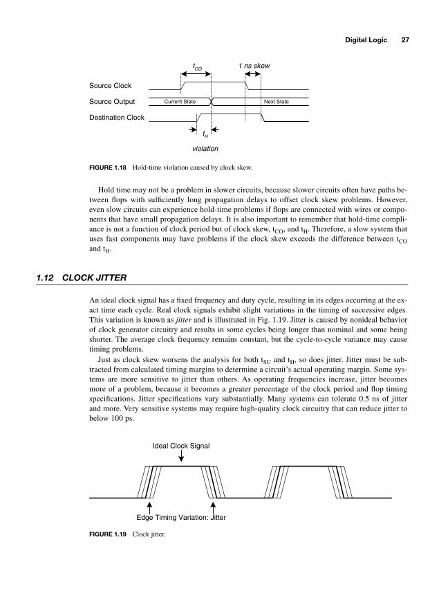
Digital Logic 27
Hold time may not be a problem in slower circuits, because slower circuits often have paths be-tween flops with sufficiently long propagation delays to offset clock skew problems. However,even slow circuits can experience hold-time problems if flops are connected with wires or compo-nents that have small propagation delays. It is also important to remember that hold-time compli-ance is not a function of clock period but of clock skew, tCO, and tH. Therefore, a slow system thatuses fast components may have problems if the clock skew exceeds the difference between tCOand tH.
1.12 CLOCK JITTER
An ideal clock signal has a fixed frequency and duty cycle, resulting in its edges occurring at the ex-act time each cycle. Real clock signals exhibit slight variations in the timing of successive edges.This variation is known as jitter and is illustrated in Fig. 1.19. Jitter is caused by nonideal behaviorof clock generator circuitry and results in some cycles being longer than nominal and some beingshorter. The average clock frequency remains constant, but the cycle-to-cycle variance may causetiming problems.
Just as clock skew worsens the analysis for both tSU and tH, so does jitter. Jitter must be sub-tracted from calculated timing margins to determine a circuit’s actual operating margin. Some sys-tems are more sensitive to jitter than others. As operating frequencies increase, jitter becomesmore of a problem, because it becomes a greater percentage of the clock period and flop timingspecifications. Jitter specifications vary substantially. Many systems can tolerate 0.5 ns of jitterand more. Very sensitive systems may require high-quality clock circuitry that can reduce jitter tobelow 100 ps.
Source Clock
Destination Clock
Source Output Current State
tCO
Next State
tH
violation
1 ns skew
FIGURE 1.18 Hold-time violation caused by clock skew.
Ideal Clock Signal
Edge Timing Variation: Jitter
FIGURE 1.19 Clock jitter.
-Balch.book Page 27 Thursday, May 15, 2003 3:46 PM

28 Digital Fundamentals
1.13 DERIVED LOGICAL BUILDING BLOCKS
Basic logic gates and flops can be combined to form more complex structures that are treated asbuilding blocks when designing larger digital systems. There are various common functions that anengineer does not want to redesign from scratch each time. Some of the common building blocks aremultiplexers, demultiplexers, tri-state buffers, registers, and shift registers. Counters represent an-other building block alluded to in the previous discussion of synchronous logic. A counter is a com-bination of flops and gates that can count either up or down, depending on the implementation.
Multiplexers, sometimes called selectors, are combinatorial elements that function as a multiposi-tion logical switches to select one of many inputs. Figure 1.20 shows a common schematic represen-tation of a multiplexer, often shortened to mux. A mux has an arbitrary number of data inputs, oftenan even power of two, and a smaller number of selector inputs. According to the binary state of theselector inputs, a specific data input is transferred to the output.
Muxes are useful, because logic circuits often need to choose between multiple data values. Acounter, for example, may choose between loading a next count value or loading an arbitrary valuefrom external logic. A possible truth table for a 4-to-1 mux is shown in Table 1.15. Each selector in-put value maps to one, and only one, data input.
A demultiplexer, also called a demux, performs the inverse operation of a mux by transferring asingle input to the output that is selected by select inputs. A demux is drawn similarly to a mux, asshown in Fig. 1.21.
TABLE 1.15 Four-to-One Multiplexer Truth Table
S1 S0 Y
0 0 A
0 1 B
1 0 C
1 1 D
A
B
C
D
Y
S1 S0
FIGURE 1.20 Four-to-one multiplexer.
A
B
C
D
Din
S1 S0
FIGURE 1.21 One-to-four demultiplexer.
-Balch.book Page 28 Thursday, May 15, 2003 3:46 PM

Digital Logic 29
A possible truth table for a 1-to-4 demux is shown in Table 1.16. Those outputs that are not se-lected are held low. The output that is selected assumes the state of the data input.
A popular use for a demux is as a decoder. The main purpose of a decoder is not so much to trans-fer an input to one of several outputs but simply to assert one output while not asserting those thatare not selected. This function has great utility in microprocessor address decoding, which involvesselecting one of multiple devices (e.g., a memory chip) at a time for access. The truth table for a 2-to-4 decoder is shown in Table 1.17. The decoder’s outputs are active-low, because most memoryand microprocessor peripheral chips use active-low enable signals.
Tri-state buffers are combinatorial elements that can drive three out-put states rather than the standard 0 and 1 states. The third state isoff, often referred to as high-impedance, hi-Z, or just Z. Tri-statebuffers enable multiple devices to share a common output wire bycooperatively agreeing to have only one device drive the wire at anyone time, during which all other devices remain in hi-Z. A tri-statebuffer is drawn as shown in Fig. 1.22.
A tri-state buffer passes its D-input to Y-output when enabled.Otherwise, the output will be turned off as shown in Table 1.18.
Electrically, tri-state behavior allows multiple tri-state buffers to be connected to the same wirewithout contention. Contention normally results when multiple outputs are connected together be-cause some want to drive high and some low. This creates potentially damaging electrical contention(a short circuit). However, if multiple tri-state buffers are connected, and only one at a time is en-abled, there is no possibility of contention. The main advantage here is that digital buses in comput-
TABLE 1.16 One-to-Four Demultiplexer Truth Table
S1 S0 A B C D
0 0 Din 0 0 0
0 1 0 Din 0 0
1 0 0 0 Din 0
1 1 0 0 0 Din
TABLE 1.17 Two-to-Four Decoder Truth Table
S1 S0 A B C D
0 0 0 1 1 1
0 1 1 0 1 1
1 0 1 1 0 1
1 1 1 1 1 0
EN
D Y
FIGURE 1.22 Tri-state buffer.
-Balch.book Page 29 Thursday, May 15, 2003 3:46 PM

30 Digital Fundamentals
ers can be arbitrarily expanded by adding more devices without the need to add a full set of input oroutput signals each time a new device is added. In a logical context, a bus is a collection of wires thatserve a common purpose. For example, a computer’s data bus might be eight wires that travel to-gether and collectively represent a byte of data. Electrical contention on a bus is often called a bus-fight. Schematically, multiple tri-state buffers might be drawn as shown in Fig. 1.23.
Each tri-state buffer contains its own enable signal, which is usually driven by some type of de-coder. The decoder guarantees that only one tri-state buffer is active at any one time, preventing con-tention on the common wire.
Registers are collections of multiple flops arranged in a group with a common function. They area common synchronous-logic building block and are commonly found in multiples of 8-bit widths,thereby representing a byte, which is the most common unit of information exchange in digital sys-tems. An 8-bit register provides a common clock and clock enable for all eight internal flops. Theclock enable allows external control of when the flops get reloaded with new D-input values andwhen they retain their current values. It is common to find registers that have a built-in tri-statebuffer, allowing them to be placed directly onto a shared bus without the need for an additional tri-state buffer component.
Whereas normal registers simply store values, synchronous elements called shift registers manip-ulate groups of bits. Shift registers exist in all permutations of serial and parallel inputs and outputs.The role of a shift register is to somehow change the sequence of bits in an array of bits. This in-cludes creating arrays of bits from a single bit at a time (serial input) or distributing an array of bitsone bit at a time (serial output). A serial-in, parallel-out shift register can be implemented by chain-ing several flops together as shown in Fig. 1.24.
TABLE 1.18 Tri-state Buffer Truth Table
EN D Y
0 x Z
1 0 0
1 1 1
FIGURE 1.23 Multiple tri-state buffers on a sin-gle wire.
Clk
DinDout[3]
Dout[1]Dout[0]
Dout[2]
DQ
DQ
DQ
DQ
FIGURE 1.24 Serial-in, parallel-out shift register.
-Balch.book Page 30 Thursday, May 15, 2003 3:46 PM
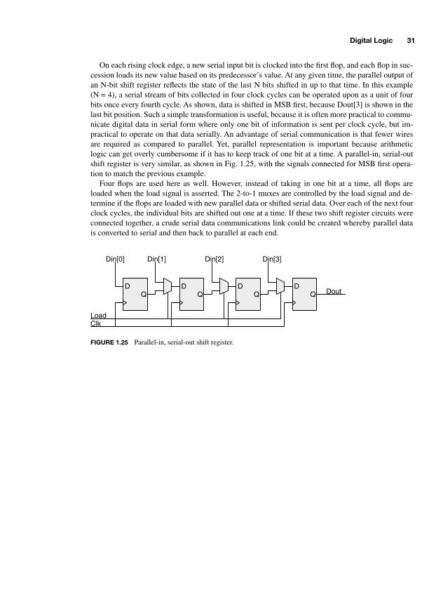
Digital Logic 31
On each rising clock edge, a new serial input bit is clocked into the first flop, and each flop in suc-cession loads its new value based on its predecessor’s value. At any given time, the parallel output ofan N-bit shift register reflects the state of the last N bits shifted in up to that time. In this example(N = 4), a serial stream of bits collected in four clock cycles can be operated upon as a unit of fourbits once every fourth cycle. As shown, data is shifted in MSB first, because Dout[3] is shown in thelast bit position. Such a simple transformation is useful, because it is often more practical to commu-nicate digital data in serial form where only one bit of information is sent per clock cycle, but im-practical to operate on that data serially. An advantage of serial communication is that fewer wiresare required as compared to parallel. Yet, parallel representation is important because arithmeticlogic can get overly cumbersome if it has to keep track of one bit at a time. A parallel-in, serial-outshift register is very similar, as shown in Fig. 1.25, with the signals connected for MSB first opera-tion to match the previous example.
Four flops are used here as well. However, instead of taking in one bit at a time, all flops areloaded when the load signal is asserted. The 2-to-1 muxes are controlled by the load signal and de-termine if the flops are loaded with new parallel data or shifted serial data. Over each of the next fourclock cycles, the individual bits are shifted out one at a time. If these two shift register circuits wereconnected together, a crude serial data communications link could be created whereby parallel datais converted to serial and then back to parallel at each end.
Dout
Clk
DQ
DQ
DQ
DQ
Load
Din[0] Din[1] Din[2] Din[3]
FIGURE 1.25 Parallel-in, serial-out shift register.
-Balch.book Page 31 Thursday, May 15, 2003 3:46 PM

This page intentionally left blank.

33
CHAPTER 2
Integrated Circuits and the 7400 Logic Families
Once basic logic design theory is understood, the next step is transferring that knowledge to a practi-cal context that includes real components. This chapter explains what an integrated circuit is andhow off-the-shelf components can be used to implement arbitrary logic functions.
Integrated circuits, called
chips
by engineers and laymen alike, are what enable digital systems aswe know them. The chapter begins with an introduction to how chips are constructed. Familiaritywith basic chip fabrication techniques and terminology enables an engineer to comprehend the dis-tinctions between various products so that their capabilities can be more readily evaluated.
A survey of packaging technology follows to provide familiarity with the common physical char-acteristics of commercially available chips. Selecting a package that is appropriate for a particulardesign can be as critical as selecting the functional parameters of the chip itself. It is important to un-derstand the variety of available chip packages and why different types of packages are used for dif-ferent applications.
The chapter’s major topic follows next: the 7400 logic families. These off-the-shelf logic chipshave formed the basis of digital systems for decades and continue to do so, although in fewer num-bers as a result of the advent of denser components. 7400 family features are presented along withcomplete examples of how the chips are applied in real designs. The purpose of this discussion is toimpart a practical and immediately applicable understanding of how digital system design can be ex-ecuted with readily available components. Although these devices are not appropriate for every ap-plication, many basic problems can be solved with 7400 chips once it is understood how to employthem.
Having seen how real chips can be used to solve actual design problems, a closely related topic ispresented at the end of this chapter: the interpretation of data sheets. Manufacturers’ data sheets con-tain critical information that must be understood to ensure a working design. An understanding ofhow data sheets are organized and the types of information that they contain is a necessary knowl-edge base for every engineer.
2.1 THE INTEGRATED CIRCUIT
Digital logic and electronic circuits derive their functionality from electronic switches called
transis-tors
. Roughly speaking, the transistor can be likened to an electronically controlled valve wherebyenergy applied to one connection of the valve enables energy to flow between two other connections.By combining multiple transistors, digital logic building blocks such as AND gates and flip-flops areformed. Transistors, in turn, are made from
semiconductors
. Consult a periodic table of elements ina college chemistry textbook, and you will locate semiconductors as a group of elements separatingthe metals and nonmetals. They are called semiconductors because of their ability to behave as both
-Balch.book Page 33 Thursday, May 15, 2003 3:46 PM
Copyright 2003 by The McGraw-Hill Companies, Inc. Click Here for Terms of Use.
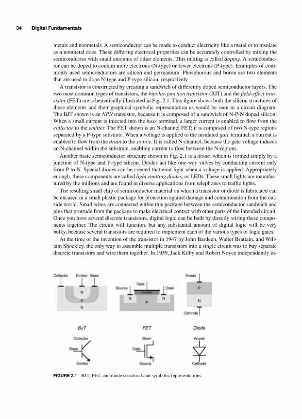
34 Digital Fundamentals
metals and nonmetals. A semiconductor can be made to conduct electricity like a metal or to insulateas a nonmetal does. These differing electrical properties can be accurately controlled by mixing thesemiconductor with small amounts of other elements. This mixing is called
doping
. A semiconduc-tor can be doped to contain more electrons (N-type) or fewer electrons (P-type). Examples of com-monly used semiconductors are silicon and germanium. Phosphorous and boron are two elementsthat are used to dope N-type and P-type silicon, respectively.
A transistor is constructed by creating a sandwich of differently doped semiconductor layers. Thetwo most common types of transistors, the
bipolar-junction transistor
(BJT) and the
field-effect tran-sistor
(FET) are schematically illustrated in Fig. 2.1. This figure shows both the silicon structures ofthese elements and their graphical symbolic representation as would be seen in a circuit diagram.The BJT shown is an
NPN
transistor, because it is composed of a sandwich of N-P-N doped silicon.When a small current is injected into the
base
terminal, a larger current is enabled to flow from the
collector
to the
emitter
. The FET shown is an N-channel FET; it is composed of two N-type regionsseparated by a P-type substrate. When a voltage is applied to the insulated
gate
terminal, a current isenabled to flow from the
drain
to the
source
. It is called N-channel, because the gate voltage inducesan N-channel within the substrate, enabling current to flow between the N-regions.
Another basic semiconductor structure shown in Fig. 2.1 is a
diode,
which is formed simply by ajunction of N-type and P-type silicon. Diodes act like one-way valves by conducting current onlyfrom P to N. Special diodes can be created that emit light when a voltage is applied. Appropriatelyenough, these components are called
light emitting diodes
, or LEDs. These small lights are manufac-tured by the millions and are found in diverse applications from telephones to traffic lights.
The resulting small chip of semiconductor material on which a transistor or diode is fabricated canbe encased in a small plastic package for protection against damage and contamination from the out-side world. Small wires are connected within this package between the semiconductor sandwich andpins that protrude from the package to make electrical contact with other parts of the intended circuit.Once you have several discrete transistors, digital logic can be built by directly wiring these compo-nents together. The circuit will function, but any substantial amount of digital logic will be verybulky, because several transistors are required to implement each of the various types of logic gates.
At the time of the invention of the transistor in 1947 by John Bardeen, Walter Brattain, and Will-iam Shockley, the only way to assemble multiple transistors into a single circuit was to buy separatediscrete transistors and wire them together. In 1959, Jack Kilby and Robert Noyce independently in-
FIGURE 2.1 BJT, FET, and diode structural and symbolic representations.
-Balch.book Page 34 Thursday, May 15, 2003 3:46 PM
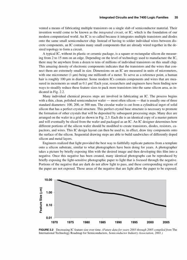
Integrated Circuits and the 7400 Logic Families 35
vented a means of fabricating multiple transistors on a single slab of semiconductor material. Theirinvention would come to be known as the
integrated circuit
, or IC, which is the foundation of ourmodern computerized world. An IC is so called because it integrates multiple transistors and diodesonto the same small semiconductor chip. Instead of having to solder individual wires between dis-crete components, an IC contains many small components that are already wired together in the de-sired topology to form a circuit.
A typical IC, without its plastic or ceramic package, is a square or rectangular silicon die measur-ing from 2 to 15 mm on an edge. Depending on the level of technology used to manufacture the IC,there may be anywhere from a dozen to tens of millions of individual transistors on this small chip.This amazing density of electronic components indicates that the transistors and the wires that con-nect them are extremely small in size. Dimensions on an IC are measured in units of micrometers,with one micrometer (1 µm) being one millionth of a meter. To serve as a reference point, a humanhair is roughly 100 µm in diameter. Some modern ICs contain components and wires that are mea-sured in increments as small as 0.1 µm! Each year, researchers and engineers have been finding newways to steadily reduce these feature sizes to pack more transistors into the same silicon area, as in-dicated in Fig. 2.2.
Many individual chemical process steps are involved in fabricating an IC. The process beginswith a thin, clean, polished semiconductor wafer — most often silicon — that is usually one of threestandard diameters: 100, 200, or 300 mm. The circular wafer is cut from a cylindrical ingot of solidsilicon that has a perfect crystal structure. This perfect crystal base structure is necessary to promotethe formation of other crystals that will be deposited by subsequent processing steps. Many dice arearranged on the wafer in a grid as shown in Fig. 2.3. Each die is an identical copy of a master patternand will eventually be sliced from the wafer and packaged as an IC. An IC designer determines howdifferent portions of the silicon wafer should be modified to create transistors, diodes, resistors, ca-pacitors, and wires. This IC design layout can then be used to, in effect, draw tiny components ontothe surface of the silicon. Sequential drawing steps are able to build sandwiches of differently dopedsilicon and metal layers.
Engineers realized that light provided the best way to faithfully replicate patterns from a templateonto a silicon substrate, similar to what photographers have been doing for years. A photographertakes a picture by briefly exposing film with the desired image and then developing this film into anegative. Once this negative has been created, many identical photographs can be reproduced bybriefly exposing the light-sensitive photographic paper to light that is focused through the negative.Portions of the negative that are dark do not allow light to pass, and these corresponding regions ofthe paper are not exposed. Those areas of the negative that are light allow the paper to be exposed.
0.01
0.10
1.00
10.00
1970 1975 1980 1985 1990 1995 2000 2005
Fea
ture
Siz
e (µ
m)
FIGURE 2.2 Decreasing IC feature size over time. (Future data for years 2003 through 2005 compiled from TheInternational Technology Roadmap for Semiconductors, Semiconductor Industry Association, 2001.)
-Balch.book Page 35 Thursday, May 15, 2003 3:46 PM

36 Digital Fundamentals
When the paper is developed in a chemical bath, portions of the paper that were exposed changecolor and yield a visible image.
Photographic processes provide excellent resolution of detail. Engineers apply this same principlein fabricating ICs to create details that are fractions of a micron in size. Similar to a photographicnegative, a mask is created for each IC processing step. Like a photographic negative, the mask doesnot have to be the same size as the silicon area it is to expose because, with lenses, light can be fo-cused through the mask to an arbitrary area. Using a technique called
photolithography,
the siliconsurface is first prepared with a light-sensitive chemical called
photoresist
. The prepared surface isthen exposed to light through the mask. Depending on whether a positive or negative photoresistprocess is employed, the areas of photoresist that have been either exposed or not exposed to lightare washed away in a chemical bath, resulting in a pattern of bare and covered areas of silicon. Thewafer can then be exposed to chemical baths, high temperature metal vapors, and ion beams. Onlythe bare areas that have had photoresist washed away are affected in this step. In this way, specificareas of the silicon wafer can be doped according to the IC designers’ specifications. Successivemask layers and process steps can continue to wash away and expose new layers of photoresist andthen build sandwiches of semiconductor and metal material. A very simplified view of these processsteps is shown in Fig. 2.4. The semiconductor fabrication process must be performed in a clean-room environment to prevent minute dust particles and other contaminants from disturbing the li-thography and chemical processing steps.
In reality, dozens of such steps are necessary to fabricate an IC. The semiconductor structures thatmust be formed by layering different metals and dopants are complex and must be formed one thinlayer at a time. Modern ICs typically have more than four layers of metal, each layer separated fromothers by a thin insulating layer of silicon dioxide. The use of more metal layers increases the cost ofan IC, but it also increases its density, because more metal wires can be fabricated to connect moretransistors. This complete process from start to finish usually takes one to four weeks. The chemicaldiffusion step (5) is an example of how different regions of the silicon wafer are doped to achievevarying electrical characteristics. In reality, several successive doping steps are required to createtransistors. The metal deposition step (10) is an example of how the microscopic metal wires thatconnect the many individual transistors are created. Hot metal vapors are passed over the preparedsurface of the wafer. Over time, individual molecules adhere to the exposed areas and form continu-ous wires. Historically, most metal interconnects on silicon ICs are made from aluminum. However,copper has become a common component of leading-edge ICs.
As IC feature sizes continue to shrink, the physical properties of light can become limiting factorsin the resolution with which a wafer can be processed. Shorter light wavelengths are necessary to
Silicon Ingot
SiliconWafer
Dice Patternedonto Wafer
FIGURE 2.3 Silicon wafer.
-Balch.book Page 36 Thursday, May 15, 2003 3:46 PM

Integrated Circuits and the 7400 Logic Families 37
meet the demands of leading-edge IC process technology. The human eye can detect electromag-netic energy from about 700 nm (red) to 400 nm (violet). Whereas ultraviolet light (< 400 nm) wasonce adequate for IC fabrication, deep UV wavelengths are now in use, and shorter wavelengths be-low 200 nm are being explored.
Each of the process steps is applied to the entire wafer. The many dice on a single wafer are usu-ally exposed to light through the same mask. The mask is either large enough to cover the entire wa-fer and therefore expose all dice at once, or the mask is stepped through the dice grid (using amachine appropriately called a
stepper
) such that each die location is exposed separately before thenext processing step. In certain cases, such as small-volume or experimental runs, different die loca-tions on the same wafer will be exposed with different masks. This is entirely feasible but may notbe as efficient as creating a wafer on which all dice are identical.
When an IC is designed and fabricated, it generally follows one of two main transistor technolo-gies: bipolar or metal-oxide semiconductor (MOS). Bipolar processes create BJTs, whereas MOSprocesses create FETs. Bipolar logic was more common before the 1980s, but MOS technologies
silicon substrate
photoresist
(1) (2) (3)
(4)
wash
(5)
chemical diffusion
(6)
wash
(7)
photoresist
(8)
mask #2
mask #1
(9)
wash
(10)
metal deposition
(11)
wash
FIGURE 2.4 The IC fabrication process.
-Balch.book Page 37 Thursday, May 15, 2003 3:46 PM
38 Digital Fundamentals
have since accounted the great majority of digital logic ICs. N-channel FETs are fabricated in anNMOS process, and P-channel FETs are fabricated in a PMOS process. In the 1980s, complemen-tary-MOS, or CMOS, became the dominant process technology and remains so to this day. CMOSICs incorporate both NMOS and PMOS transistors.
2.2 IC PACKAGING
When the wafer has completed its final process step, it is tested and then sliced up to separate the in-dividual dice. Dice that fail the initial testing are quickly discarded. Those that pass inspection arereadied for packaging. A package is necessary for several reasons, including protection of the die andthe creation of electromechanical connections with other circuitry. ICs are almost always mountedonto a circuit board, and it is usually difficult to mount unpackaged ICs directly to the board. How-ever, there are special situations in which ICs are not packaged and are directly attached to the board.These cases are often at opposite ends of the technological spectrum. At the low end of technology,ICs can be several process generations behind the current state of the art. Therefore, the relative com-plexity of mounting them to a circuit board may not be as great. The savings of direct mounting are inspace and cost. A common quartz wristwatch benefits from direct mounting, because the small con-fines of a watch match very well with the space savings achieved by not requiring a package for theIC. These watch ICs use mature semiconductor process technologies. At the high end of technology,some favorable electrical and thermal characteristics can be achieved by eliminating as much inter-mediate bulk as possible between individual ICs and supporting circuitry. However, the technical dif-ficulties of direct-mounting a leading-edge IC can be challenging and greatly increase costs.Therefore, direct-mounting of all but very low-end electronics is relatively rare.
IC packaging technology has evolved dramatically from the early days, yet many mature packagetypes still exist and are in widespread use. Plastic and ceramic are the two most common materialsused in an IC package. They surround the die and its lead frame. The lead frame is a structure of metalwires that fan out from the die and extend to the package exterior as pins for connection to a circuitboard. Plastic packages are generally lower in cost as compared to ceramics, but they have poorerthermal performance. Thermal characteristics are important for ICs that handle large currents and dis-sipate large quantities of heat. To prevent the IC from overheating, the heat must be conducted and ra-diated away as efficiently as possible. Ceramic material conducts heat far better than plastic.
A very common package is the
dual in-line package
, or DIP, shown in Fig. 2.5. A DIP has twoparallel rows of pins that are spaced on 0.1-in centers. Each pin extends roughly 0.2 in below thebottom of the plastic or ceramic body. Pins are numbered sequentially from 1 going left to rightalong one side and resuming on the opposite side from right to left. There is usually at least one pin1 marker at one end of the package. It is either a dot near pin 1 or a semicircular indentation on oneedge of the package.
DIPs are commonly manufactured in standard sizes ranging from 6 to 48 pins, and some manu-facturers go beyond 48 pins. Smaller pin-count devices have 0.3-in wide packages, and larger de-vices are 0.6 in wide. Because of the ubiquity of the DIP, there are many variations of pin counts andpackage widths. For many years, the DIP accounted for the vast majority of digital logic packages.Common logic ICs were manufactured in 14- and 16-pin DIPs. Memory ICs were manufactured in16-, 18-, 24-, and 28-pin DIPs. Microprocessors were available in 40-, 44-, and 48-pin DIPs. DIPsare still widely available today, but their use as a percentage of the total IC market has declinedmarkedly. However, the benefits of the DIP remain: they are inexpensive and easy to work with byhand, eliminating the need for costly assembly tools.
If you were to carefully crack open a DIP, you would be able to see the mechanical assembly ofthe die and lead frame. This is illustrated in Fig. 2.6. The die is cemented in the center of a stamped
-Balch.book Page 38 Thursday, May 15, 2003 3:46 PM

Integrated Circuits and the 7400 Logic Families 39
metal frame and is connected to the individual pins with extremely thin wires. Once the electricalconnections are made, the fragile assembly is encased in a plastic or ceramic body for protection andthe exterior portions of the pins are folded vertically.
All other IC packages are variations on this theme. Some packages use a similar lead-frame struc-ture, whereas more advanced packages utilize very high-quality miniature circuit boards made fromeither ceramic or fiberglass.
An oft-quoted attribute of ICs is that their density doubles every 18 months as a result of improve-ments in process technology. This prediction was made in 1965 by Dr. Gordon Moore, a co-founderof Intel. It has since come to be known as
Moore’s law,
because the semiconductor industry hasmatched this prediction over time. Before to the explosion of IC density, the semiconductor industryclassified ICs into several categories depending on the number of logic gates on the device:
small-scale integration
(SSI),
medium-scale integration
(MSI),
large-scale integration
(LSI), and, finally,
very large-scale integration
(VLSI). Figure 2.7 provides a rough definition of these terms. As thedensity of ICs continued to grow at a rapid pace, it became rather ridiculous to keep adding wordslike “very” and “extra” to these categories, and the terms’ widespread use declined. ICs are now of-ten categorized based on their minimum feature size and metal process. For example, one might re-fer to an IC as “0.25 µm, three-layer metal (aluminum)” or “0.13 µm, six-layer copper.”
side viewend view
top view
pin 1 8
916
FIGURE 2.5 A 16-pin dual in-line package.
die
FIGURE 2.6 DIP lead frame.
-Balch.book Page 39 Thursday, May 15, 2003 3:46 PM

40 Digital Fundamentals
As IC densities grew at this tremendous pace, the number of pins on each IC and the speed atwhich they operated began to increase as well. DIPs soon become a limiting factor in the perfor-mance of ICs. First, the addition of more pins made the package longer, because there are only tworows of pins. However, most chips are relatively square in shape to minimize on-chip interconnec-tion distances. This creates a conflict: a long, narrow package that is unsuitable for increasing squaredie sizes. Second, the lengths of some pins in the DIP lead frame, especially those near the corners,are relatively long. This has an adverse impact on the quality of high-speed signals. Third, the 0.1-inpin spacing on DIPs keeps them artificially large as circuit board technologies continue improving tohandle smaller contacts.
One solution to the pin density problem was the development of the
pin grid array
, or PGA, pack-age. Shown in Fig. 2.8, the PGA is akin to a two-dimensional DIP with pins spaced on 0.1-in cen-ters. Very high pin counts are achievable with a PGA, because all of its area is usable rather than justthe perimeter. Being a square, the PGA is compatible with large ICs, because it more closelymatches the proportions of a silicon chip.
The PGA provides high pin density, but its drawback is relatively high cost. Two lower-cost pack-ages were developed for ICs that require more pins than DIPs but fewer pins than found on a PGA:the
small outline integrated circuit
(SOIC) and the
plastic leaded chip carrier
(PLCC). Examples ofSOIC and PLCC packages are shown in Fig. 2.9. Both SOICs and PLCCs feature pins on a 0.05-inpitch — half that of a DIP or PGA. The SOIC is basically a shrunken DIP with shorter pins that arefolded parallel to the plane of the package instead of protruding down vertically. This enables theSOIC to be surface mounted onto the circuit board by soldering the pins directly to metal pads on theboard. By contrast, a DIP requires that holes be drilled in the board for the pins to be soldered into.The SOIC represents an improvement in packaging density and ease of manufacture over DIPs, butit is still limited to relatively simple ICs due to its one-dimensional pin arrangement.
PLCCs increase pin density and ease the design of the lead frame by utilizing a two-dimensionalpin arrangement. Higher pin counts (68, 84, and 96 pins) were enabled by the PLCC, and its square
1
10
100
1000
10,000
100,000
1,000,000
SSI MSI LSI VLSI
Tra
nsis
tors
per
Chi
p
FIGURE 2.7 Relative component count of ICs.
FIGURE 2.8 Pin grid array package.
-Balch.book Page 40 Thursday, May 15, 2003 3:46 PM
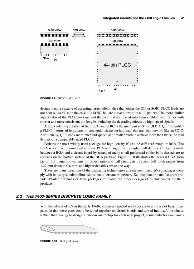
Integrated Circuits and the 7400 Logic Families 41
design is more capable of accepting larger silicon dice than either the DIP or SOIC. PLCC leads arenot bent outward, as in the case of a SOIC, but are curved inward in a “J” pattern. The more similaraspect ratio of the PLCC package and the dice that are placed into them enabled lead frames withshorter and more consistent pin lengths, reducing the degrading effects on high-speed signals.
A higher-density relative of the PLCC and SOIC is the
quad flat pack
, or QFP. A QFP resemblesa PLCC in terms of its square or rectangular shape but has leads that are bent outward like an SOIC.Additionally, QFP leads are thinner and spaced at a smaller pitch to achieve more than twice the leaddensity of a comparably sized PLCC.
Perhaps the most widely used package for high-density ICs is the
ball grid array
, or BGA. TheBGA is a surface mount analog to the PGA with significantly higher ball density. Contact is madebetween a BGA and a circuit board by means of many small preformed solder balls that adhere tocontacts on the bottom surface of the BGA package. Figure 2.10 illustrates the general BGA formfactor, but numerous variants on aspect ratio and ball pitch exist. Typical ball pitch ranges from1.27 mm down to 0.8 mm, and higher densities are on the way.
There are many variations of the packaging technologies already mentioned. Most packages com-ply with industry standard dimensions, but others are proprietary. Semiconductor manufacturers pro-vide detailed drawings of their packages to enable the proper design of circuit boards for theirproducts.
2.3 THE 7400-SERIES DISCRETE LOGIC FAMILY
With the advent of ICs in the early 1960s, engineers needed ready access to a library of basic logicgates so that these gates could be wired together on circuit boards and turned into useful products.Rather than having to design a custom microchip for each new project, semiconductor companies
side view end view
top view
side view
top view
pin 1
44-pin PLCCpin 1
FIGURE 2.9 SOIC and PLCC.
FIGURE 2.10 Ball grid array.
-Balch.book Page 41 Thursday, May 15, 2003 3:46 PM
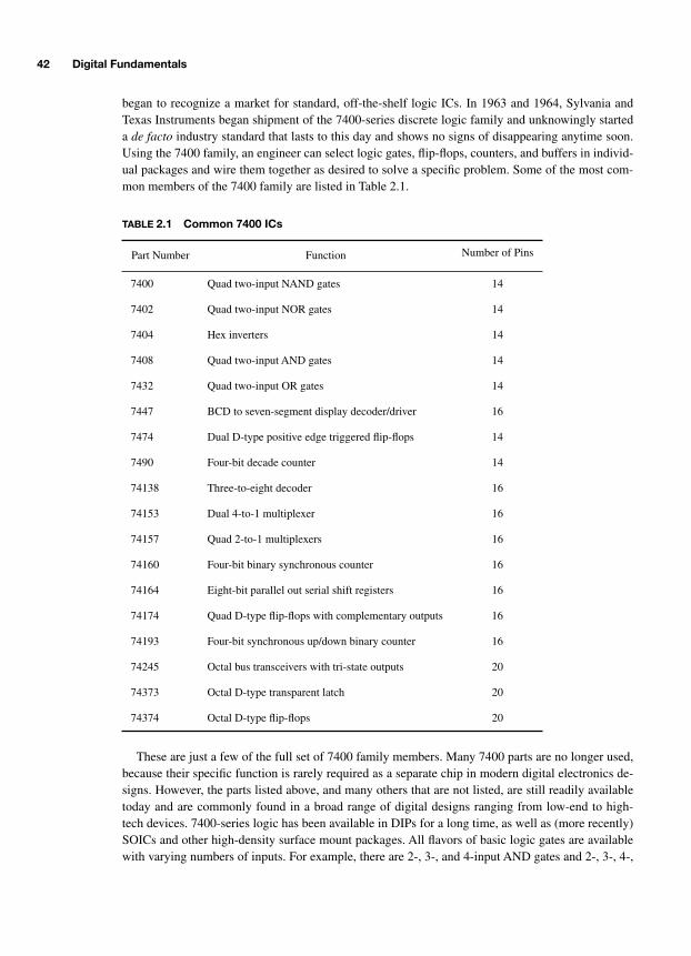
42 Digital Fundamentals
began to recognize a market for standard, off-the-shelf logic ICs. In 1963 and 1964, Sylvania andTexas Instruments began shipment of the 7400-series discrete logic family and unknowingly starteda
de facto
industry standard that lasts to this day and shows no signs of disappearing anytime soon.Using the 7400 family, an engineer can select logic gates, flip-flops, counters, and buffers in individ-ual packages and wire them together as desired to solve a specific problem. Some of the most com-mon members of the 7400 family are listed in Table 2.1.
These are just a few of the full set of 7400 family members. Many 7400 parts are no longer used,because their specific function is rarely required as a separate chip in modern digital electronics de-signs. However, the parts listed above, and many others that are not listed, are still readily availabletoday and are commonly found in a broad range of digital designs ranging from low-end to high-tech devices. 7400-series logic has been available in DIPs for a long time, as well as (more recently)SOICs and other high-density surface mount packages. All flavors of basic logic gates are availablewith varying numbers of inputs. For example, there are 2-, 3-, and 4-input AND gates and 2-, 3-, 4-,
TABLE
2.1 Common 7400 ICs
Part Number Function Number of Pins
7400 Quad two-input NAND gates 14
7402 Quad two-input NOR gates 14
7404 Hex inverters 14
7408 Quad two-input AND gates 14
7432 Quad two-input OR gates 14
7447 BCD to seven-segment display decoder/driver 16
7474 Dual D-type positive edge triggered flip-flops 14
7490 Four-bit decade counter 14
74138 Three-to-eight decoder 16
74153 Dual 4-to-1 multiplexer 16
74157 Quad 2-to-1 multiplexers 16
74160 Four-bit binary synchronous counter 16
74164 Eight-bit parallel out serial shift registers 16
74174 Quad D-type flip-flops with complementary outputs 16
74193 Four-bit synchronous up/down binary counter 16
74245 Octal bus transceivers with tri-state outputs 20
74373 Octal D-type transparent latch 20
74374 Octal D-type flip-flops 20
-Balch.book Page 42 Thursday, May 15, 2003 3:46 PM

Integrated Circuits and the 7400 Logic Families 43
8-, 12-, and 13-input NAND gates. There are numerous varieties of flip-flops, counters, multiplexers,shift registers, and bus transceivers. Flip-flops exist with and without complementary outputs, pre-set/clear inputs, and independent clocks. Counters are available in 4-bit blocks that can both incre-ment and decrement and count to either 15 (binary counter) or 9 (decade counter) before restartingthe count at 0. Shift registers exist in all permutations of serial and parallel inputs and outputs. Bustransceivers in 4- and 8-bit increments exist with different types of output enables and capabilities tofunction in unidirectional or bidirectional modes. Bus transceivers enable the creation and expansionof tri-state buses on which multiple devices can communicate.
One interesting IC is the 7447 seven-segment display driver. This component allows the creationof graphical numeric displays in applications such as counters and timers. Seven-segment displaysare commonly seen in automobiles, microwave ovens, watches, and consumer electronics. Seven in-dependent on/off elements can represent all ten digits as shown in Fig. 2.11. The 7447 is able todrive an LED-based seven-segment display when given a
binary coded decimal
(BCD) input. BCDis a four-bit binary number that has valid values from 0 through 9. Hexadecimal values from 0xAthrough 0xF are not considered legal BCD values.
Familiarity with the 7400 series proves very useful no matter what type of digital system you aredesigning. For low-end systems, 7400-series logic may be the only type of IC at your disposal tosolve a wide range of problems. At the high end, many people are often surprised to see a small 14-pin 7400-series IC soldered to a circuit board alongside a fancy 32-bit microprocessor running at100 MHz. The fact is that the basic logic functions that the 7400 series offers are staples that have di-rect applications at all levels of digital systems design. It is time well spent to become familiar withthe extensive capabilities of the simple yet powerful 7400 family. Manufacturers’ logic data books,either in print or on line, are invaluable references. It can be difficult to know ahead of time if a de-sign may call for one more gate to function properly; that is when a 40-year old logic family cansave the day.
2.4 APPLYING THE 7400 FAMILY TO LOGIC DESIGN
Applications of the 7400 family are truly infinite, because the various ICs represent basic buildingblocks rather than complete solutions. Up through the early 1980s, it was common to see computersystems constructed mainly from interconnected 7400-series ICs along with a few LSI componentssuch as a microprocessor and a few memory chips. These days, most commercial digital systems aredesigned using some form of higher-density logic IC, either fully custom or user programmable.However, the engineer or hobbyist who has a relatively small-scale logic problem to solve, and whomay not have access to more expensive custom or programmable logic ICs, may be able to utilizeonly 7400 logic in an efficient and cost-effective solution. Two examples follow to provide insightinto how 7400 building blocks can be assembled to solve logic design problems.
A hypothetical example is a logic circuit to examine three switches and turn on an LED if two andonly two of the three switches are turned on. The truth table for such a circuit is as follows in
FIGURE 2.11 Seven-segment display.
-Balch.book Page 43 Thursday, May 15, 2003 3:46 PM

44 Digital Fundamentals
Table 2.2, given that A, B, and C are the inputs, and an LED is the active-low output (assume that theLED is turned on by driving a logic 0 rather than a logic 1).
This LED driver truth table can be converted into the following Boolean logic equation with a Kar-naugh map or simply by inspection:
After consulting a list of available 7400 logic ICs, three become attractive for our application: the7404 inverter, 7408 AND, and 7432 OR. The LED driver logic equation requires four inverters, sixtwo-input AND gates, and two 2-input OR gates. Four ICs are required, because a 7404 provides sixinverters, a 7408 provides four AND gates, and a 7432 contains four OR gates. These four ICs canbe connected according to a
schematic diagram
as shown in Fig. 2.12. A schematic diagram illus-trates the electrical connectivity scheme of various components. Each component is identified by a
reference designator
consisting of a letter followed by a number. ICs are commonly identified byreference designators beginning with the letter “U”. Additionally, each component has numerouspins that are numbered on the diagram. These pin numbers conform to the IC manufacturer’s num-bering scheme. Each of these 7400-series ICs has 14 pins. Another convention that remains from bi-polar logic days is the use of the label VCC to indicate the positive voltage supply node. GNDrepresents ground—the common, or return, voltage supply node.
All ICs require connections to a power source. In this circuit, +5 V serves as the power supply, be-cause the 7400 family is commonly manufactured in a bipolar semiconductor process requiring a+5-V supply. The four rectangular blocks at the top of the diagram represent this power connectioninformation. Because this schematic diagram shows individual gates, the gates’ reference designa-tors contain an alphabetic suffix to identify unique instances of gates within the same IC. Not allgates in each IC are actually used. Those that are unused are tied inactive by connecting their inputsto a valid logic level—in this case, ground. It would be equally valid to connect the inputs of unusedgates to the positive supply voltage, +5 V.
This logic circuit would work, but a more efficient solution is available to those who are familiarwith the capabilities of the 7400 family. The 7411 provides three 3-input AND gates, which is per-fect for this application, allowing a reduction in the part count to three ICs instead of four. This cir-
TABLE
2.2 LED Driver Logic Truth Table
A B C LED
0 0 0 1
0 0 1 1
0 1 0 1
0 1 1 0
1 0 0 1
1 0 1 0
1 1 0 0
1 1 1 1
LED ABC ABC ABC+ +=
-Balch.book Page 44 Thursday, May 15, 2003 3:46 PM
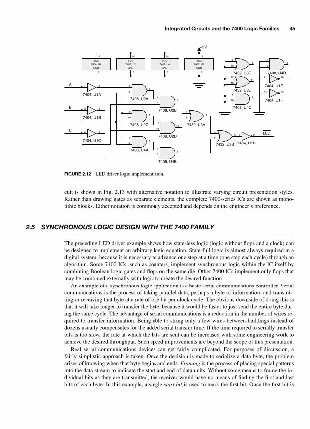
Integrated Circuits and the 7400 Logic Families 45
cuit is shown in Fig. 2.13 with alternative notation to illustrate varying circuit presentation styles.Rather than drawing gates as separate elements, the complete 7400-series ICs are shown as mono-lithic blocks. Either notation is commonly accepted and depends on the engineer’s preference.
2.5 SYNCHRONOUS LOGIC DESIGN WITH THE 7400 FAMILY
The preceding LED driver example shows how state-less logic (logic without flops and a clock) canbe designed to implement an arbitrary logic equation. State-full logic is almost always required in adigital system, because it is necessary to advance one step at a time (one step each cycle) through analgorithm. Some 7400 ICs, such as counters, implement synchronous logic within the IC itself bycombining Boolean logic gates and flops on the same die. Other 7400 ICs implement only flops thatmay be combined externally with logic to create the desired function.
An example of a synchronous logic application is a basic serial communications controller. Serialcommunications is the process of taking parallel data, perhaps a byte of information, and transmit-ting or receiving that byte at a rate of one bit per clock cycle. The obvious downside of doing this isthat it will take longer to transfer the byte, because it would be faster to just send the entire byte dur-ing the same cycle. The advantage of serial communications is a reduction in the number of wires re-quired to transfer information. Being able to string only a few wires between buildings instead ofdozens usually compensates for the added serial transfer time. If the time required to serially transferbits is too slow, the rate at which the bits are sent can be increased with some engineering work toachieve the desired throughput. Such speed improvements are beyond the scope of this presentation.
Real serial communications devices can get fairly complicated. For purposes of discussion, afairly simplistic approach is taken. Once the decision is made to serialize a data byte, the problemarises of knowing when that byte begins and ends.
Framing
is the process of placing special patternsinto the data stream to indicate the start and end of data units. Without some means to frame the in-dividual bits as they are transmitted, the receiver would have no means of finding the first and lastbits of each byte. In this example, a single
start bit
is used to mark the first bit. Once the first bit is
7404, U1A
7404, U1B
7404, U1C
7408, U2A
7408, U2B
7408, U2C
7408, U2D
7408, U4A
7408, U4B
7432, U3A
7432, U3B 7404, U1D
7404, U1F
7404, U1E
7408, U4D
7408, U4C
7432, U3C
7432, U3D
VCC
14
GND
7
7404, U1VCC
14
GND
7
7408, U2VCC
14
GND
7
7408, U4VCC
14
GND
7
7432, U3
+5V
A
B
CLED
1 2
3 4
5 69 8
11 10
13 12
13
2
46
5
13
2
46
5
98
10
1211
13
98
10
1211
13
98
10
1211
13
13
2
46
5
FIGURE 2.12 LED driver logic implementation.
-Balch.book Page 45 Thursday, May 15, 2003 3:46 PM

46 Digital Fundamentals
detected, the last bit is found by knowing that there are eight bits in a byte. During periods of inactiv-ity, an idle communications interface is indicated by a persistent logic 0. When the transmitter isgiven a byte to send, it first drives a logic-1 start bit and then sends eight data bits. Each bit is sent inits own clock cycle. Therefore, nine clock cycles are required to transfer each byte. The serial inter-face is composed of two signals,
clock
and
serial data
, and functions as shown in Fig. 2.14.The eight data bits are sent from least-significant bit, bit 0, to most-significant bit, bit 7, following
the start bit. Following the transmission of bit 7, it is possible to immediately begin a new byte by in-serting a new start bit. This timing diagram does not show a new start bit directly following bit 7.The corresponding output of the receiver is shown in Fig. 2.15. Here,
data out
is the eight-bit quan-
A
B
C
LED
GND7
4Y8
1A1
1Y2
32A
42Y
VCC
6A
6Y
5A
14
13
12
11
7404U1
3A5
5Y10
3Y6
4A9
GND7
3Y8
1A1
1B2
32A
42B
VCC
1C
1Y
3C
14
13
12
11
7411U2
2C5
3B10
2Y6
3A9
GND7
3Y8
1A1
1B2
31Y
42A
VCC
4B
4A
4Y
14
13
12
11
7432U3
2B5
3B10
2Y6
3A9
+5V +5V
+5V
FIGURE 2.13 LED driver logic using 74111 with fewer ICs.
D7D6D5D4D3D2D1D0
FIGURE 2.14 Serial interface bit timing.
ClockDataOut
Data
Ready
x Data x
FIGURE 2.15 Serial receive output timing.
-Balch.book Page 46 Thursday, May 15, 2003 3:46 PM
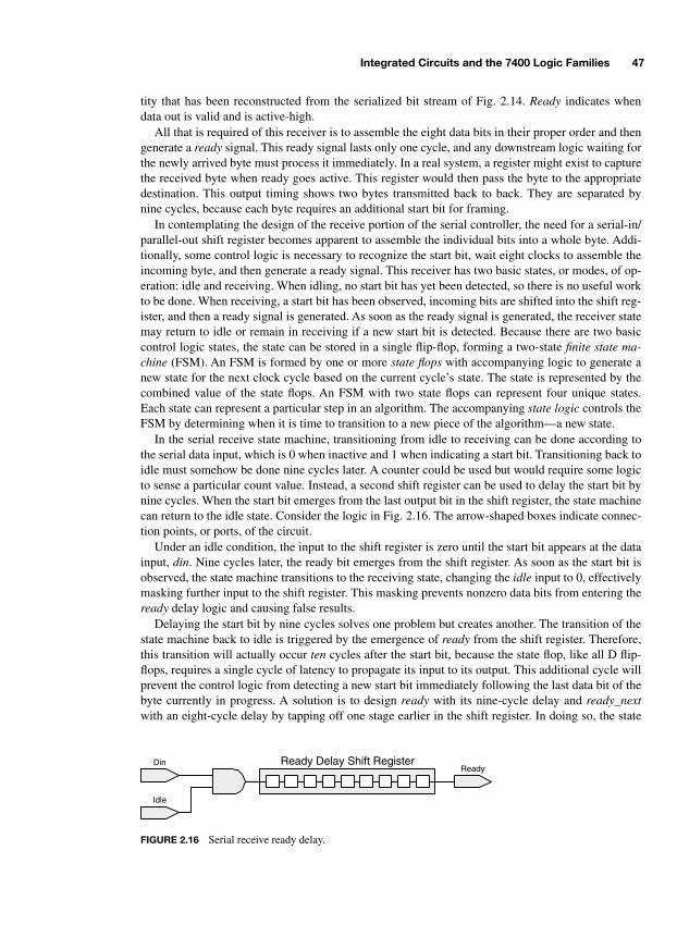
Integrated Circuits and the 7400 Logic Families 47
tity that has been reconstructed from the serialized bit stream of Fig. 2.14.
Ready
indicates whendata out is valid and is active-high.
All that is required of this receiver is to assemble the eight data bits in their proper order and thengenerate a
ready
signal. This ready signal lasts only one cycle, and any downstream logic waiting forthe newly arrived byte must process it immediately. In a real system, a register might exist to capturethe received byte when ready goes active. This register would then pass the byte to the appropriatedestination. This output timing shows two bytes transmitted back to back. They are separated bynine cycles, because each byte requires an additional start bit for framing.
In contemplating the design of the receive portion of the serial controller, the need for a serial-in/parallel-out shift register becomes apparent to assemble the individual bits into a whole byte. Addi-tionally, some control logic is necessary to recognize the start bit, wait eight clocks to assemble theincoming byte, and then generate a ready signal. This receiver has two basic states, or modes, of op-eration: idle and receiving. When idling, no start bit has yet been detected, so there is no useful workto be done. When receiving, a start bit has been observed, incoming bits are shifted into the shift reg-ister, and then a ready signal is generated. As soon as the ready signal is generated, the receiver statemay return to idle or remain in receiving if a new start bit is detected. Because there are two basiccontrol logic states, the state can be stored in a single flip-flop, forming a two-state
finite state ma-chine
(FSM). An FSM is formed by one or more
state flops
with accompanying logic to generate anew state for the next clock cycle based on the current cycle’s state. The state is represented by thecombined value of the state flops. An FSM with two state flops can represent four unique states.Each state can represent a particular step in an algorithm. The accompanying
state logic
controls theFSM by determining when it is time to transition to a new piece of the algorithm—a new state.
In the serial receive state machine, transitioning from idle to receiving can be done according tothe serial data input, which is 0 when inactive and 1 when indicating a start bit. Transitioning back toidle must somehow be done nine cycles later. A counter could be used but would require some logicto sense a particular count value. Instead, a second shift register can be used to delay the start bit bynine cycles. When the start bit emerges from the last output bit in the shift register, the state machinecan return to the idle state. Consider the logic in Fig. 2.16. The arrow-shaped boxes indicate connec-tion points, or ports, of the circuit.
Under an idle condition, the input to the shift register is zero until the start bit appears at the datainput,
din
. Nine cycles later, the ready bit emerges from the shift register. As soon as the start bit isobserved, the state machine transitions to the receiving state, changing the
idle
input to 0, effectivelymasking further input to the shift register. This masking prevents nonzero data bits from entering the
ready
delay logic and causing false results.Delaying the start bit by nine cycles solves one problem but creates another. The transition of the
state machine back to idle is triggered by the emergence of
ready
from the shift register. Therefore,this transition will actually occur
ten
cycles after the start bit, because the state flop, like all D flip-flops, requires a single cycle of latency to propagate its input to its output. This additional cycle willprevent the control logic from detecting a new start bit immediately following the last data bit of thebyte currently in progress. A solution is to design
ready
with its nine-cycle delay and
ready_next
with an eight-cycle delay by tapping off one stage earlier in the shift register. In doing so, the state
ReadyDin
Idle
Ready Delay Shift Register
FIGURE 2.16 Serial receive ready delay.
-Balch.book Page 47 Thursday, May 15, 2003 3:46 PM
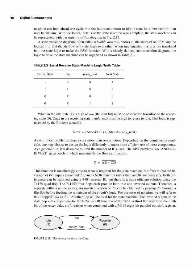
48 Digital Fundamentals
machine can look ahead one cycle into the future and return to idle in time for a new start bit thatmay be arriving. With the logical details of the state machine now complete, the state machine canbe represented with the
state transition diagram
in Fig. 2.17.A state transition diagram, often called a
bubble diagram
, shows all the states of an FSM and thelogical
arcs
that dictate how one state leads to another. When implemented, the arcs are translatedinto the state logic to make the FSM function. With a clearly defined state transition diagram, thelogic to drive the state machine can be organized as shown in Table 2.3.
When in the idle state (1), a high on
din
(the start bit) must be observed to transition to the receiv-ing state (0). Once in the receiving state,
ready_next
must be high to return to idle. This logic is rep-resented by the Boolean equation,
As with most problems, there exists more than one solution. Depending on the components avail-able, one may choose to design the logic differently to make more efficient use of those components.As a general rule, it is desirable to limit the number of ICs used. The 7451 provides two “AND-OR-INVERT” gates, each of which implements the Boolean function,
This function is tantalizingly close to what is required for the state machine. It differs in that the in-version of two inputs (
state
and
din
) and a NOR function rather than an OR are necessary. Both dif-ferences can be resolved using a 7404 inverter IC, but there is a more efficient solution using the74175 quad flop. The 74175’s four flops each provide both true and inverted outputs. Therefore, aseparate 7404 is not necessary. An inverted version of
din
can be obtained by passing
din
through aflip-flop before feeding the remainder of the circuit’s logic. For purposes of notation, we will refer tothis “flopped”
din
as
din´
. Another flop will be used for the state machine. The inverted output of thestate flop will compensate for the NOR vs. OR function of the 7451. A third flop will form the ninthbit of the
ready
delay shift register when combined with a 74164 eight-bit parallel-out shift register.
TABLE
2.3 Serial Receive State Machine Logic Truth Table
Current State din ready_next Next State
1 0 X 1
1 1 X 0
0 X 0 0
0 X 1 1
Idle(1)
Receive(0)
din
ready_next
FIGURE 2.17 Serial receive state machine.
Next State&Din( ) State&ready_next( )+=
Y AB CD+=
-Balch.book Page 48 Thursday, May 15, 2003 3:46 PM

Integrated Circuits and the 7400 Logic Families 49
Conveniently, the 74164 contains an internal AND gate at its input to implement the idle-enable ofthe start bit into the shift register.
The total parts count for this serial receiver is four 7400-family ICs: two 74164 shift registers, one7451 AND-OR-INVERT, and one 74175 quad flop. One flop and one-half of the 7451 are unused inthis application. Figure 2.18 shows how these ICs are connected to implement the serial receivelogic. Note that a mixed-style of IC representation is used: most ICs are shown in a single block, butthe 74175 is broken into separate flops for clarity. Even if an IC is represented as a single block, it isnot necessary to draw the individual pins in the order in which they physically appear. As with theprevious example, the graphical representation of logic depends on individual discretion. In additionto being functionally and electrically correct, a schematic diagram should be easy to understand.
All synchronous elements, the shift registers and flops, are driven by an input clock signal, clk.The synchronous elements involved in the control path of the logic are also reset at the beginning ofoperation with the active-low reset_ signal. Reset_ is necessary to ensure that the state flop and theready_next delay logic begin in an idle state when power is first applied. This is necessary, becauseflip-flops power up in a random, hence unknown, state. Once they are explicitly reset, they hold theirstate until the logic specifically changes their state. The shift register in the data path, U3, does notrequire a reset, because its contents are not used until eight valid data bits are shifted in, therebyflushing the eight bits with random power-up states. It would not hurt to connect U3’s clr_ pin toreset_, but this is not done to illustrate the option that is available. In certain logic implementations,adding reset capability to a flop may incur a penalty in terms of additional cost or circuit size. Whena reset function is not free, it may be decided not to reset certain flops if their contents do not need tobe guaranteed at power up, as is the case here.
A1
B2
QA
QB
QC
QD
3
4
5
6
VCC
14
74164U3
CLK8
CLR_9
QE
QF
QG
QH
10
11
12
13GND
7
1A1
1B13
91C
101D
1Y
2Y
8
6
VCC
14
7451U2
2A2
2B3
42C
52D
NC
NC
12
11
GND
7
A1
B2
QA
QB
QC
QD
3
4
5
6
VCC
14
74164U4
CLK8
CLR_9
QE
QF
QG
QH
10
11
12
13GND
7
D4
Q2
74175
Q_3
U1A
D5
Q7
74175
Q_6
U1B
D12
Q10
74175
Q_11
U1C
D13
Q15
74175
Q_14
U1D
CLK9 VCC
16
CLR_1
GND
8
74175U1
+5V
+5V
+5V
Din
Clk
Reset_
Ready
Dout[7:0]
Dout[7]
Dout[6]
Dout[5]
Dout[4]
Dout[3]
Dout[2]
Dout[1]
Dout[0]
ready_next
state
din'
+5V
FIGURE 2.18 Serial receive logic schematic diagram.
-Balch.book Page 49 Thursday, May 15, 2003 3:46 PM
50 Digital Fundamentals
In this logic circuit, the inverted output of the state flop, U1B, is used as the state bit to compen-sate for the 7451’s NOR function. The unused clr_ and b pins of U3 are connected to +5 V to renderthem neutral on the shift register’s behavior. The shift register will not clear itself, because clr_ is ac-tive-low and, similarly, the internal input AND-gate that combines a and b, will be logically by-passed by tying b to logic 1. The parallel byte output of this serial receiver is designated Dout[7:0]and is formed by grouping the eight outputs of the shift register into a single bus. One common nota-tion for assigning members of a bus is to connect each individual member to a thicker line with sometype of bus-ripper line. The bus ripper is often drawn in the schematic diagram as mitered or curvedat the bus end to make its function more visually apparent.
Designing an accompanying serial transmitter follows a very similar design process to the preced-ing discussion. It is left as an exercise to the reader.
2.6 COMMON VARIANTS OF THE 7400 FAMILY
In the 1970s and 1980s, the 7400 family was commonly manufactured in a bipolar semiconductorprocess that operated using a +5-V power supply and was known as transistor-transistor logic (TTL).The discussion of the 7400 family thus far has included only the original +5-V bipolar type. The7400’s popularity and broad application to digital design has kept it relevant through many improve-ments in semiconductor process technology. As engineers learned to fabricate faster and more effi-cient ICs, the 7400 was redesigned in many different process generations beginning in the late1960s. Some of the more common 7400 variants are briefly discussed here.
The original 7400 discrete TTL logic family featured typical propagation delays of 10 ns per gateand power consumption, also called power dissipation, of approximately 10 mW per gate. By mod-ern standards, the 7400’s speed is relatively slow, and its power dissipation is relatively high. In-creasing system complexity dictates deeper logic: more gates chained together to implement morecomplex Boolean functions. Each added level of logic adds at least another gate’s worth of propaga-tion delay. At the same time, power consumption also becomes a problem. Ten milliwatts may notsound like a lot of power, but, when multiplied by several thousand gates, it represents a substantialdesign problem in terms of both supplying a large quantity of power and cooling the radiated heatfrom digital systems.
Two notable bipolar variants of the 7400 are the 74LS and 74F families. The 74LS, LS indicatinglow-power Schottky, has speed comparable to that of the original 7400, but it dissipates roughly 20percent of its power. The 74F, F indicating fast, is approximately 80 percent faster than the 7400 andreduces power consumption by almost half. Whether the concern is reducing power or increasingspeed, these two families are useful for applications requiring 5-V bipolar technology.
CMOS technology began to emerge in the 1980s as a popular process for fabricating digital ICsas a result of its lower power consumption as compared to bipolar. The low-power characteristics ofCMOS logic stem from the fact that a FET requires essentially no current to keep it in an on or offstate (unlike a BJT, which always draws some current when it is turned on). A CMOS gate, there-fore, will draw current only when it switches. For this reason, the power consumption of a CMOSlogic gate is extremely low in an idle, or quiescent, state and increases with the frequency at which itswitches.
Several CMOS 7400 families were introduced, among them being the 74HCT and 74ACT, eachof which has power consumption orders of magnitude less than bipolar equivalents at low frequen-cies. Earlier CMOS versions of the 7400 were not fully compatible with the bipolar devices, becauseof voltage threshold differences between the CMOS and bipolar processes. A typical TTL output isonly guaranteed to rise above 2.5 V, depending on output loading. In contrast, a typical 5-V CMOSinput requires a minimum level of around 3 V to guarantee detecting a logic 1. This inconsistency in
-Balch.book Page 50 Thursday, May 15, 2003 3:46 PM
Integrated Circuits and the 7400 Logic Families 51
voltage range causes a fundamental problem in which a TTL gate driving an ordinary CMOS gatecannot be guaranteed to operate in all situations. Both the 74HCT and 74ACT families possess thelow-power benefits of CMOS technology and retain compatibility with bipolar ICs. A 74HCT deviceis somewhat slower than a 74LS equivalent, and the 74ACT is faster than a 74LS device.
There has been an explosion of 7400 variants. Most of the families introduced in the last decadeare based on CMOS technology and are tailored to a broad set of applications ranging from simplespeed to high-power bus drivers. Most types of 7400 devices share common pin-outs and functions,with the exception of some proprietary specialized parts that may be produced by only a single man-ufacturer. Most of the 7400 families still require +5-V supplies, but lower voltages such as 3.3 V,2.5 V, 1.8 V, and 1.5 V are available as well. These lower-voltage families are important because ofthe general trend toward lower voltages for digital logic.
2.7 INTERPRETING A DIGITAL IC DATA SHEET
Semiconductor manufacturers publish data sheets for each of their products. Regardless of the spe-cific family or device, all logic IC data sheets share common types of information. Once the basicdata sheet terminology and organization is understood, it is relatively easy to figure out other datasheets even when their exact terminology changes. Data sheet structure is illustrated using the74LS00 from Fairchild Semiconductor as an example. A page from its data sheet is shown in Fig.2.19.
Digital IC data sheets should have at least two major sections: functional description and electri-cal specifications. The functional description usually contains the device pin assignment, or pin-out,as well as a detailed discussion of how the part logically operates. A simple IC such as the 74LS00will have a very brief functional description, because there is not much to say about a NAND gate’soperation. More complex ICs such as microprocessors can have functional descriptions that fill doz-ens or hundreds of pages and are broken into many chapters. Some data sheets add additional sec-tions to present the mechanical dimensions of the package and its thermal properties. Digital ICelectrical specifications are similar across most types of devices and often appear in the followingfour categories:
• Absolute maximum ratings. As the term implies, these parameters specify the absolute extremesthat the IC may be subjected to without sustaining permanent damage. Manufacturers almost uni-versally state that the IC should never be operated under these extreme conditions. These ratingsare useful, because they indicate how the device may be stored and express the quality of designand manufacture of the physical chip. Manufacturers specify a storage temperature range withinwhich the semiconductor structures will not break down. In the case of Fairchild’s 74LS00, thisrange is –65 to 150°C. Maximum voltage levels are also specified, 7 V in the case of the 74LS00,indicating that the device may be subjected to a 7-V potential without destructing.
• Recommended operating conditions. These parameters specify the normal range of voltages andtemperatures that the IC should be operated within such that its functionality is guaranteed to meetspecifications set forth by the manufacturer. Two of the most important specifications in this sec-tion are the supply voltage (commonly labeled as either VCC or VDD, depending on whether a bipo-lar or MOS process) and the operating temperature. An IC may have multiple supply voltagespecifications, because an IC can actually operate on several different voltages simultaneously.Each supply voltage may power a different portion of the chip. When the manufacturer specifiessupply voltage, it does so with a certain tolerance, usually either ±5 or ±10 percent. Many 5-Vlogic ICs are guaranteed to operate only at a supply voltage from 4.75 to 5.25 V (±5 percent). Op-erating temperature is very important, because it affects the timing of the device. As a semiconduc-
-Balch.book Page 51 Thursday, May 15, 2003 3:46 PM

52 Digital Fundamentals
FIGURE 2.19 74LS00 manufacturer’s specifications. (Reprinted with permission from Fairchild Semiconductor and NationalSemiconductor.)
-Balch.book Page 52 Thursday, May 15, 2003 3:46 PM
Integrated Circuits and the 7400 Logic Families 53
tor heats up, it slows down. As it cools, its speed increases. Outside of the recommended operatingtemperature, the device is not guaranteed to function, because the effects of temperature becomeso severe that functionality is compromised. There are four common temperature ranges for ICs:commercial (0 to 70°C), industrial (–40 to 85°C), automotive (–40 to 125°C), and military (–55 to125°C). It is more difficult to manufacture an IC that operates over wider temperature ranges. Assuch, more demanding temperature grades are often more expensive than the commercial grade.
Other parameters establish the safe operating limits for input signals as well as the applied volt-age thresholds that represent logic 0 and 1 states. Minimum and maximum input levels are ex-pressed as either absolute voltages or voltages relative to the supply voltage pins of the device.Exceeding these voltages may damage the device. Logic threshold specifications are provided toensure that the logic input voltages are such that the device will function as intended and not con-fuse a 1 for a 0, or vice versa. There is also a limit to how must current a digital output can drive.Current output specifications should be known so that a chip is not overloaded, which could resultin either permanent damage to the chip or the chip’s failure to meet its published specifications.
• DC electrical characteristics. DC parameters specify the voltages and currents that the IC willpresent to other circuitry to which it is connected. Whereas recommended operating conditionsspecify the environment under which the chip will properly operate, DC electrical characteristicsspecify the environment that the chip itself will create. Output voltage specifications define thelogic 0 and 1 thresholds that the chip is guaranteed to drive under all legal operating conditions.These specifications confirm that the chip is compatible with other chips in the same family andalso allow an engineer to determine if the output levels are compatible with another chip that itmay be driving.
Input current specifications characterize the load that the chip presents to whatever circuit isdriving it. When either logic state is applied to the chip, a small current flows between the driverand the chip in question. Quantifying these currents enables an engineer to ensure compatibilitybetween multiple ICs. When one IC drives several other ICs, the sum of the input currents shouldnot exceed the output current specification of the driver.
• AC electrical characteristics or switching characteristics). AC parameters often represent thegreatest complexity and level of detail in a digital IC’s specifications. They are the guaranteedtiming parameters of inputs and outputs. If the IC is purely combinatorial (e.g., 74LS00), timingmay just be matter of specifying propagation delays and rise and fall times. Logic ICs with syn-chronous elements (e.g., flops) have associated parameters such as setup, hold, clock frequency,and output valid times.
Keep in mind that each manufacturer has a somewhat different style of presenting these specifica-tions. The necessary information should exist, but data sheet sections may be named differently; theymay include certain information in different groupings, and terminology may be slightly different.
Specifications may be provided in mixed combinations of minimum, typical/nominal, andmaximum. When a minimum or maximum limit is not specified, it is understood to be self-evi-dent or subject to a physical limitation that is beyond the scope of the device. Using Fairchild’s74LS00 as an example, no minimum output current is specified, because the physical minimumis very near zero. The actual output current is determined by the load that is being driven, assum-ing that the load draws no more than the specified maximum. Other specifications are shown un-der certain operating conditions. A well written data sheet provides guaranteed specificationsunder worst-case conditions. Here, the logic 1 output voltage (VOH) is specified as a minimum of2.5 V under conditions of minimum supply voltage (VCC), maximum output current (IOH), andmaximum logic-low input voltage (VIL). These are worst-case conditions. When VCC decreases,so will VOH. When IOH increases, it places a greater load on the output, dragging it down to itslowest level.
-Balch.book Page 53 Thursday, May 15, 2003 3:46 PM

54 Digital Fundamentals
Timing specifications may also be incomplete. Manufacturers do not always guarantee minimumor maximum parameters, depending on the specific type of device and the particular specification.As with DC voltages, worst-case parameters should always be specified. When a minimum or maxi-mum delay is not specified, it is generally because that parameter is of secondary importance, andthe manufacturer was unable to control its process to a sufficient level of detail to guarantee thatvalue. In many situations where incomplete specifications are given, there are acceptable reasons fordoing so, and the lack of information does not hurt the quality of the design.
Typical timing numbers are not useful in many circumstances, because they do not represent alimit of the device’s operation. A thorough design must take into account the best and worst perfor-mance of each IC in the circuit so that one can guarantee that the circuit will function under all con-ditions. Therefore, worst-case timing parameters are usually the most important to consider first,because they are the dominant limit of a digital system’s performance in most cases. In more ad-vanced digital systems, minimum parameters can become equally as important because of the needto meet hold time and thereby ensure that a signal does not disappear too quickly before the drivenIC can properly sense the signal’s logic level.
Output timing specifications are often specified with an assumed set of loading conditions, be-cause the current drawn by the load has an impact on the output driver’s ability to establish a validlogic level. A small load will enable the IC to switch its output faster, because less current is de-manded of the output. A heavier load has the opposite effect, because it draws more current, whichplaces a greater strain on the output driver.
-Balch.book Page 54 Thursday, May 15, 2003 3:46 PM
55
CHAPTER 3
Basic Computer Architecture
Microprocessors are central components of almost all digital systems, because combinations ofhardware and software are used to solve design problems. A computer is formed by combining a mi-croprocessor with a mix of certain basic elements and customized logic. Software runs on a micro-processor and provides a flexible framework that orchestrates the behavior of hardware that has beencustomized to fit the application. When many people think about computers, images of desktop PCsand laptops come to their minds. Computers are much more diverse than the stereotypical image andpermeate everyday life in increasing numbers. Small computers control microwave ovens, tele-phones, and CD players.
Computer architecture is fundamental to the design of digital systems. Understanding how a basiccomputer is designed enables a digital system to take shape by using a microprocessor as a centralcontrol element. The microprocessor becomes a programmable platform upon which the major com-ponents of an algorithm can be implemented. Digital logic can then be designed to surround the mi-croprocessor and assist the software in carrying out a specific set of tasks.
The first portion of this chapter explains the basic elements of a computer, including the micro-processor, memory, and input/output devices. Basic microprocessor operation is presented from ahardware perspective to show how instructions are executed and how interaction with other systemcomponents is handled. Interrupts, registers, and stacks are introduced as well to provide an overallpicture of how computers function. Following this basic introduction is a complete example of howan actual eight-bit computer might be designed, with detailed descriptions of bus operation and ad-dress decoding.
Once basic computer architecture has been discussed, common techniques for improving andaugmenting microprocessor capabilities are covered, including direct memory access and bus expan-sion. These techniques are not relegated to high-end computing but are found in many smaller digitalsystems in which it is more economical to add a little extra hardware to achieve feature and perfor-mance goals instead of having to use a microprocessor that may be too complex and more expensivethan desired.
The chapter closes with an introduction to assembly language and microprocessor addressingmodes. Writing software is not a primary topic of this book, but basic software design is an insepara-ble part of digital systems design. Without software, a computer performs no useful function. As-sembly language basics are presented in a general manner, because each microprocessor has its owninstruction set and assembly language, requiring specific reading focused on that particular device.Basic concepts, however, are universal across different microprocessor implementations and serve tofurther explain how microprocessors actually function.
-Balch.book Page 55 Thursday, May 15, 2003 3:46 PM
Copyright 2003 by The McGraw-Hill Companies, Inc. Click Here for Terms of Use.

56 Digital Fundamentals
3.1 THE DIGITAL COMPUTER
A digital computer is a collection of logic elements that can execute arbitrary algorithms to performdata calculation and manipulation functions. A computer is composed of a microprocessor, memory,and some input/output (I/O) elements as shown in Fig. 3.1. The microprocessor, often called a mi-croprocessor unit (MPU) or central processing unit (CPU), contains logic to step through an algo-rithm, called a
program
, that has been stored in the computer’s program memory. The data used andmanipulated by that program is held in the computer’s data memory. Memory is a repository for datathat is usually organized as a linear array of individually accessible locations. The microprocessorcan access a particular location in memory by presenting a memory address (the index of the desiredlocation) to the memory element. I/O elements enable the microprocessor to communicate with theoutside world to acquire new data and present the results of its programmed computations. Such ele-ments can include a keyboard or display controller.
Programs are composed of many very simple individual operations, called
instructions,
that spec-ify in exact detail how the microprocessor should carry out an algorithm. A simple program mayhave dozens of instructions, whereas a complex program can have tens of millions of instructions.Collectively, the programs that run on microprocessors are called
software
, in contrast to the
hard-ware
on which they run. Each type of microprocessor has its own
instruction set
that defines the fullset of unique, discrete operations that it is capable of executing. These instructions perform very nar-row tasks that, on their own, may seem insignificant. However, when thousands or millions of thesetiny instructions are strung together, they may create a video game or a word processor.
A microprocessor possesses no inherent intelligence or capability to spontaneously begin per-forming useful work. Each microprocessor is constructed with an instruction set that can be invokedin arbitrary sequences. Therefore, a microprocessor has the potential to perform useful work but willdo nothing of the sort on its own. To make the microprocessor perform useful work, it requires ex-plicit guidance in the form of software programming. A task of even moderate complexity must bebroken down into many tiny steps to be implemented on a microprocessor. These steps include basicarithmetic, Boolean operations, loading data from memory or an input element such as a keyboard,and storing data back to memory or an output element such as a printer.
Memory structure is one of a computer’s key characteristics, because the microprocessor is al-most constantly accessing it to retrieve a new instruction, load new data to operate on, or store a cal-culated result. While program and data memory are logically distinct classifications, they may sharethe same physical memory resource.
Random access memory
(RAM) is the term used to describe ageneric memory resource whose locations can be accessed, or
addressed
, in an arbitrary order andeither read or written. A
read
is the process of retrieving data from a memory address and loading itinto the microprocessor. A
write
is the process of storing data to a memory address from the micro-processor. Both programs and data can occupy RAM. Consider your desktop computer. When you
KeyboardController
Microprocessor
ProgramMemory
DataMemory
DisplayController
PrinterController
FIGURE 3.1 Generic computer block diagram.
-Balch.book Page 56 Thursday, May 15, 2003 3:46 PM

Basic Computer Architecture 57
execute a program that is located on the disk drive, that program is first loaded into the computer’sRAM and then executed from a region set aside for program memory. As on a desktop computer,RAM is most often
volatile—
meaning that it loses its contents when the power is turned off.Some software cannot be stored in volatile memory, because basic initialization instructions, or
boot code
, must be present when the computer is turned on. Remember that a microprocessor can donothing useful without software being readily available. When power is first applied to a computer,the microprocessor must be able to quickly locate boot code so that it can get itself ready to acceptinput from a user or load a program from an input device. This startup sequence is called
booting
,hence the term
boot code
. When you turn your computer on, the first messages that it displays on themonitor are a product of its boot code. Eventually, the computer is able to access its disk drive andbegins loading software into RAM as part of its normal operation. To ensure that boot code is readyat power-up,
nonvolatile
memory called
read only memory
(ROM) exists. ROM can be used to storeboth programs as well as any data that must be present at power-up and immediately accessible.Software contained in ROM is also known as
firmware
. As its name implies, ROM can only be readbut not written. More complex computers contain a relatively small quantity of ROM to hold basicboot code that then loads main operating software from another device into RAM. Small computersmay contain all of their software in ROM. Figure 3.2 shows how ROM and RAM complement eachother in a typical computer architecture.
A microprocessor connects to devices such as memory and I/O via
data
and
address buses
. Col-lectively, these two buses can be referred to as the
microprocessor bus
. A bus is a collection of wiresthat serve a common purpose. The data bus is a bit array of sufficient size to communicate one com-plete data unit at a time. Most often, the data bus is one or more bytes in width. An eight-bit micro-processor, operating on one byte at time, almost always has an eight-bit data bus. A 32-bitmicroprocessor, capable of operating on up to 4 bytes at a time, can have a data bus that is 32, 16, or8 bits wide. The exact data bus width is implementation specific and varies according to the intendedapplication of the microprocessor. A narrower bus width means that it will take more time to com-municate a quantity of data as compared to a wider bus. Common notation for a data bus is
D[7:0]
for an 8-bit bus and
D[31:0]
for a 32-bit bus, where 0 is the least-significant bit.The address bus is a bit array of sufficient size to fully express the microprocessor’s
addressspace
. Address space refers to the maximum amount of memory and I/O that a microprocessor candirectly address. If a microprocessor has a 16-bit address bus, it can address up to 2
16
= 65,536bytes. Therefore, it has a 64 kB address space. The entire address space does not have to be used; itsimply establishes a maximum limit on memory size. Common notation for a 16-bit address bus is
A[15:0]
, where 0 is the least-significant bit. Figure 3.3 shows a typical microprocessor bus configu-ration in a computer. Note that the address bus is unidirectional (the microprocessor asserts re-quested addresses to the various devices), and the data bus is bidirectional (the microprocessorasserts data on a write and the devices assert data on reads).
I/O Devices
Microprocessor
RAMROM
Boot Code Program Region Data Region
FIGURE 3.2 Basic ROM/RAM memory complement.
-Balch.book Page 57 Thursday, May 15, 2003 3:46 PM
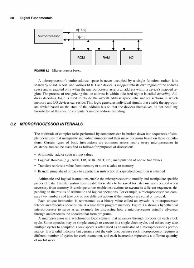
58 Digital Fundamentals
A microprocessor’s entire address space is never occupied by a single function; rather, it isshared by ROM, RAM, and various I/Os. Each device is
mapped
into its own region of the addressspace and is enabled only when the microprocessor asserts an address within a device’s mapped re-gion. The process of recognizing that an address is within a desired region is called
decoding
. Ad-dress decoding logic is used to divide the overall address space into smaller sections in whichmemory and I/O devices can reside. This logic generates individual signals that enable the appropri-ate device based on the state of the address bus so that the devices themselves do not need anyknowledge of the specific computer’s unique address decoding.
3.2 MICROPROCESSOR INTERNALS
The multitude of complex tasks performed by computers can be broken down into sequences of sim-ple operations that manipulate individual numbers and then make decisions based on those calcula-tions. Certain types of basic instructions are common across nearly every microprocessor inexistence and can be classified as follows for purposes of discussion:
•
Arithmetic: add or subtract two values
•
Logical: Boolean (e.g., AND, OR, XOR, NOT, etc.) manipulation of one or two values
•
Transfer: retrieve a value from memory or store a value to memory
•
Branch: jump ahead or back to a particular instruction if a specified condition is satisfied
Arithmetic and logical instructions enable the microprocessor to modify and manipulate specificpieces of data. Transfer instructions enable these data to be saved for later use and recalled whennecessary from memory. Branch operations enable instructions to execute in different sequences, de-pending on the results of arithmetic and logical operations. For example, a microprocessor can com-pare two numbers and take one of two different actions if the numbers are equal or unequal.
Each unique instruction is represented as a binary value called an
opcode
. A microprocessorfetches and executes opcodes one at a time from program memory. Figure 3.4 shows a hypotheticalmicroprocessor to serve as an example for discussing how a microprocessor actually advancesthrough and executes the opcodes that form programs.
A microprocessor is a synchronous logic element that advances through opcodes on each clockcycle. Some opcodes may be simple enough to execute in a single clock cycle, and others may takemultiple cycles to complete. Clock speed is often used as an indicator of a microprocessor’s perfor-mance. It is a valid indicator but certainly not the only one, because each microprocessor requires adifferent number of cycles for each instruction, and each instruction represents a different quantityof useful work.
I/O
Microprocessor
ROM RAM
A[15:0]
D[7:0]
FIGURE 3.3 Microprocessor buses.
-Balch.book Page 58 Thursday, May 15, 2003 3:46 PM
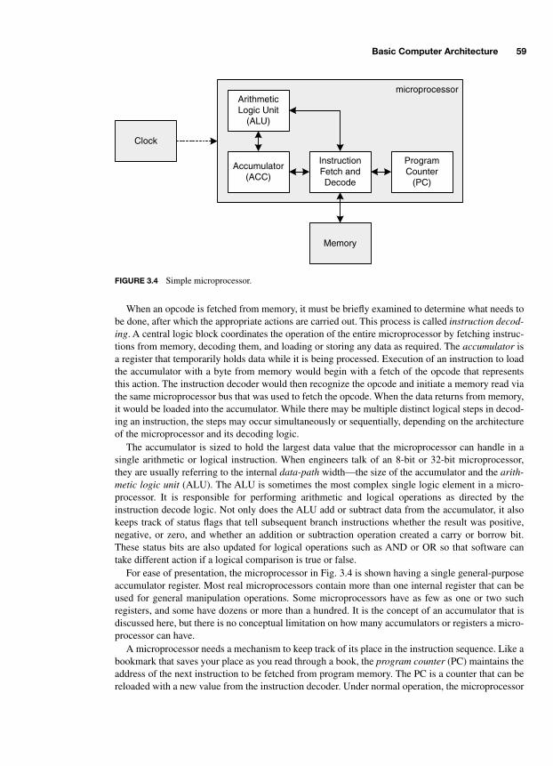
Basic Computer Architecture 59
When an opcode is fetched from memory, it must be briefly examined to determine what needs tobe done, after which the appropriate actions are carried out. This process is called
instruction decod-ing
. A central logic block coordinates the operation of the entire microprocessor by fetching instruc-tions from memory, decoding them, and loading or storing any data as required. The
accumulator
isa register that temporarily holds data while it is being processed. Execution of an instruction to loadthe accumulator with a byte from memory would begin with a fetch of the opcode that representsthis action. The instruction decoder would then recognize the opcode and initiate a memory read viathe same microprocessor bus that was used to fetch the opcode. When the data returns from memory,it would be loaded into the accumulator. While there may be multiple distinct logical steps in decod-ing an instruction, the steps may occur simultaneously or sequentially, depending on the architectureof the microprocessor and its decoding logic.
The accumulator is sized to hold the largest data value that the microprocessor can handle in asingle arithmetic or logical instruction. When engineers talk of an 8-bit or 32-bit microprocessor,they are usually referring to the internal
data-path
width—the size of the accumulator and the
arith-metic logic unit
(ALU). The ALU is sometimes the most complex single logic element in a micro-processor. It is responsible for performing arithmetic and logical operations as directed by theinstruction decode logic. Not only does the ALU add or subtract data from the accumulator, it alsokeeps track of status flags that tell subsequent branch instructions whether the result was positive,negative, or zero, and whether an addition or subtraction operation created a carry or borrow bit.These status bits are also updated for logical operations such as AND or OR so that software cantake different action if a logical comparison is true or false.
For ease of presentation, the microprocessor in Fig. 3.4 is shown having a single general-purposeaccumulator register. Most real microprocessors contain more than one internal register that can beused for general manipulation operations. Some microprocessors have as few as one or two suchregisters, and some have dozens or more than a hundred. It is the concept of an accumulator that isdiscussed here, but there is no conceptual limitation on how many accumulators or registers a micro-processor can have.
A microprocessor needs a mechanism to keep track of its place in the instruction sequence. Like abookmark that saves your place as you read through a book, the
program counter
(PC) maintains theaddress of the next instruction to be fetched from program memory. The PC is a counter that can bereloaded with a new value from the instruction decoder. Under normal operation, the microprocessor
microprocessor
InstructionFetch andDecode
ProgramCounter
(PC)
Accumulator(ACC)
ArithmeticLogic Unit
(ALU)
Memory
Clock
FIGURE 3.4 Simple microprocessor.
-Balch.book Page 59 Thursday, May 15, 2003 3:46 PM
60 Digital Fundamentals
moves through instructions sequentially. After executing each instruction, the PC is incremented,and a new instruction is fetched from the address indicated by the PC. The major exception to thislinear behavior is when branch instructions are encountered. Branch instructions exist specifically tooverride the sequential execution of instructions. When the instruction decoder fetches a branch in-struction, it must determine the condition for the branch. If the condition is met (e.g., the ALU zeroflag is asserted), the
branch target address
is loaded into the PC. Now, when the instruction decodergoes to fetch the next instruction, the PC will point to a new part of the instruction sequence insteadof simply the next program memory location.
3.3 SUBROUTINES AND THE STACK
Most programs are organized into multiple blocks of instructions called
subroutines
rather than asingle large sequence of instructions. Subroutines are located apart from the main program segmentand are invoked by a subroutine call. This call is a type of branch instruction that temporarily jumpsthe microprocessor’s PC to the subroutine, allowing it to be executed. When the subroutine has com-peted, control is returned to the program segment that called it via a return from subroutine instruc-tion. Subroutines provide several benefits to a program, including modularity and ease of reuse. Amodular subroutine is one that can be relocated in different parts of the same program while still per-forming the same basic function. An example of a modular subroutine is one that sorts a list of num-bers in ascending order. This sorting subroutine can be called by multiple sections of a program andwill perform the same operation on multiple lists. Reuse is related to modularity and takes the con-cept a step farther by enabling the subroutine to be transplanted from one program to another with-out modification. This concept greatly speeds the software development process.
Almost all microprocessors provide inherent support for subroutines in their architectures and in-struction sets. Recall that the program counter keeps track of the next instruction to be executed andthat branch instructions provide a mechanism for loading a new value into the PC. Most branch in-structions simply cause a new value to be loaded into the PC when their specific branch condition issatisfied. Some branch instructions, however, not only reload the PC but also instruct the micropro-cessor to save the current value of the PC off to the side for later recall. This stored PC value, or
sub-routine return address
, is what enables the subroutine to eventually return control to the programthat called it. Subroutine call instructions are sometimes called
branch-to-subroutine
or
jump-to-subroutine,
and they may be unconditional.When a branch-to-subroutine is executed, the PC is saved into a data structure called a
stack
. Thestack is a region of data memory that is set aside by the programmer specifically for the main pur-pose of storing the microprocessor’s state information when it branches to a subroutine. Other usesfor the stack will be mentioned shortly. A stack is a
last-in, first-out
memory structure. When data isstored on the stack, it is
pushed
on. When data is removed from the stack, it is
popped
off. Poppingthe stack recalls the most recently pushed data. The first datum to be pushed onto the stack will bethe last to be popped. A
stack pointer
(SP) holds a memory address that identifies the
top
of the stackat any given time. The SP decrements as entries are pushed on and increments at they are popped off,thereby growing the stack downward in memory as data is pushed on as shown in Fig. 3.5.
By pushing the PC onto the stack during a branch-to-subroutine, the microprocessor now has ameans to return to the calling routine at any time by restoring the PC to its previous value by simplypopping the stack. This operation is performed by a return-from-subroutine instruction. Many mi-croprocessors push not only the PC onto the stack when calling a subroutine, but the accumulatorand ALU status flags as well. While this increases the complexity of a subroutine call and returnsomewhat, it is useful to preserve the state of the calling routine so that it may resume controlsmoothly when the subroutine ends.
-Balch.book Page 60 Thursday, May 15, 2003 3:46 PM
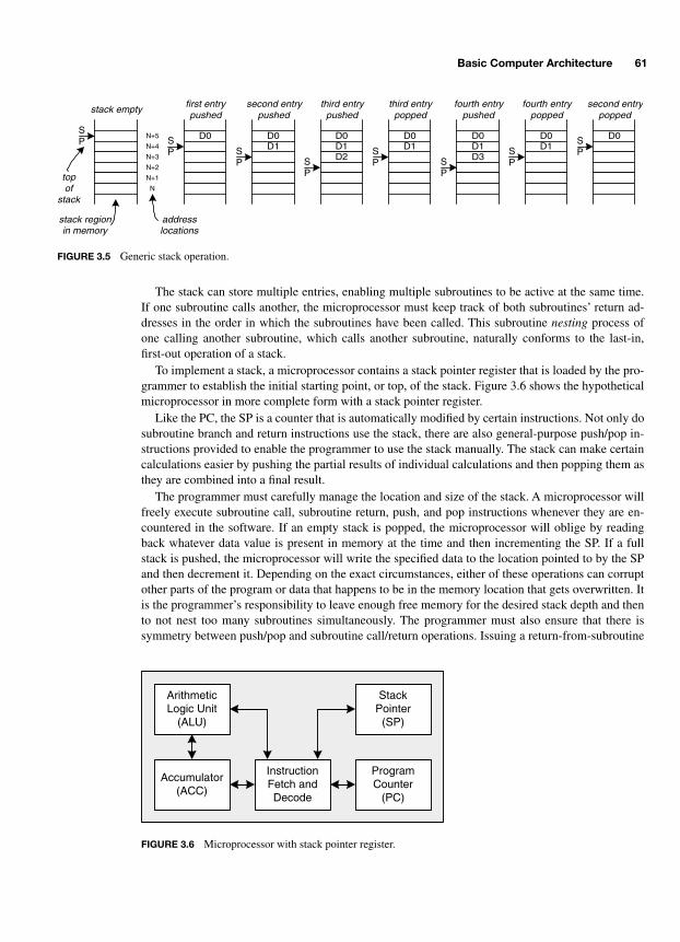
Basic Computer Architecture 61
The stack can store multiple entries, enabling multiple subroutines to be active at the same time.If one subroutine calls another, the microprocessor must keep track of both subroutines’ return ad-dresses in the order in which the subroutines have been called. This subroutine
nesting
process ofone calling another subroutine, which calls another subroutine, naturally conforms to the last-in,first-out operation of a stack.
To implement a stack, a microprocessor contains a stack pointer register that is loaded by the pro-grammer to establish the initial starting point, or top, of the stack. Figure 3.6 shows the hypotheticalmicroprocessor in more complete form with a stack pointer register.
Like the PC, the SP is a counter that is automatically modified by certain instructions. Not only dosubroutine branch and return instructions use the stack, there are also general-purpose push/pop in-structions provided to enable the programmer to use the stack manually. The stack can make certaincalculations easier by pushing the partial results of individual calculations and then popping them asthey are combined into a final result.
The programmer must carefully manage the location and size of the stack. A microprocessor willfreely execute subroutine call, subroutine return, push, and pop instructions whenever they are en-countered in the software. If an empty stack is popped, the microprocessor will oblige by readingback whatever data value is present in memory at the time and then incrementing the SP. If a fullstack is pushed, the microprocessor will write the specified data to the location pointed to by the SPand then decrement it. Depending on the exact circumstances, either of these operations can corruptother parts of the program or data that happens to be in the memory location that gets overwritten. Itis the programmer’s responsibility to leave enough free memory for the desired stack depth and thento not nest too many subroutines simultaneously. The programmer must also ensure that there issymmetry between push/pop and subroutine call/return operations. Issuing a return-from-subroutine
stack regionin memory
SP
stack empty
N
N+1
N+2
N+3
N+4
N+5
addresslocations
D0SP
first entrypushed
D0
SP
second entrypushed
D1D0
SP
third entrypushed
D1D2
third entrypopped
D0
SP
D1D0
SP
D1D3
fourth entrypushed
D0
SP
D1
fourth entrypopped
D0SP
second entrypopped
topof
stack
FIGURE 3.5 Generic stack operation.
InstructionFetch andDecode
ProgramCounter
(PC)
Accumulator(ACC)
ArithmeticLogic Unit
(ALU)
StackPointer
(SP)
FIGURE 3.6 Microprocessor with stack pointer register.
-Balch.book Page 61 Thursday, May 15, 2003 3:46 PM

62 Digital Fundamentals
instruction while already in the main program would lead to undesirable results when the micropro-cessor fetches reloads the PC with an incorrect return address.
3.4 RESET AND INTERRUPTS
Thus far, the steady-state operation of a microprocessor has been discussed in which instructions arefetched, decoded, and executed in an order determined by the PC and branch instructions. There aretwo special cases in which the microprocessor does not follow this regular pattern of operation. Thefirst case is at power-up, when the microprocessor must transition from an idle state to executing in-structions. This transition sequence is called
reset
and involves the microprocessor fetching its bootcode from memory to begin the programmed software sequence. Reset is triggered by asserting aparticular logic level onto a microprocessor pin and can occur either at power-up or at any arbitrarytime when it is desired to restart, or reboot, the microprocessor from a known initial state. Some mi-croprocessors have special instructions that can actually trigger a soft reset.
The question arises of how the microprocessor determines which instruction to execute first whenit has just been reset. To solve this problem, each microprocessor has a
reset vector
that points it to afixed, predetermined memory address where the programmer must locate the first instruction of theboot sequence. The reset vector is specified by the microprocessor’s designer. Some microprocessorslocate the reset vector at the beginning of memory and some place it toward the end of the addressspace. Sometimes the main body of the program will be located in another portion of memory, andthe first instruction at the reset vector will contain a branch instruction to jump to the desired loca-tion.
The second case in which the microprocessor does not follow the normal instruction sequence isduring normal operation when an event occurs and the programmer wishes the microprocessor topause what it is currently doing and handle the event with a special software routine. Such an eventis called an
interrupt
. A common application for an interrupt is the implementation of a periodic,timed operation such as monitoring the temperature of a room. Because the room temperature doesnot change often, the microprocessor can handle other tasks during normal operation. A timer can beset to expire every few seconds, causing an interrupt event. When the interrupt triggers, the micro-processor can read the room temperature, take any appropriate action (e.g., turn on a ventilation fan),and then resume its normal operation.
An interrupt can be triggered by asserting a special-purpose microprocessor interrupt signal. In-terrupt events can also be triggered from within a microprocessor via special instructions. When aninterrupt occurs, the microprocessor saves its state by pushing the PC and other registers onto thestack, and then the PC is loaded with an
interrupt vector
that points to an
interrupt service routine
(ISR) in memory. In this way, the interrupt process is similar to a branch-to-subroutine. However,the interrupt may be triggered by an external hardware event instead of by software. Like reset, eachinterrupt pin on the microprocessor has an interrupt vector associated with it. The programmerknows that an ISR is to be located at a specific memory location to service a particular interrupt.When the ISR has completed, a
return-from-interrupt
instruction is executed that restores the micro-processor’s prior state by popping it from the stack. Control is then returned to the routine that wasinterrupted and normal execution proceeds.
As the interrupt mechanism executes, the program that gets interrupted does not necessarily haveany knowledge of the event. Because the state of the microprocessor is saved and then restored dur-ing the return-from-interrupt, the main routine has no concept that somewhere along the way its exe-cution was paused for an arbitrary period. The programmer may choose to make such knowledgeavailable by sharing information between the ISR and other routines, but this is left to individualsoftware implementations.
-Balch.book Page 62 Thursday, May 15, 2003 3:46 PM
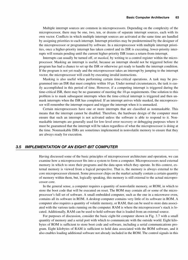
Basic Computer Architecture 63
Multiple interrupt sources are common in microprocessors. Depending on the complexity of themicroprocessor, there may be one, two, ten, or dozens of separate interrupt sources, each with itsown vector. Conflicts in which multiple interrupt sources are activated at the same time are handledby assigning priorities to each interrupt. Interrupt priorities may be predetermined by the designer ofthe microprocessor or programmed by software. In a microprocessor with multiple interrupt priori-ties, once a higher-priority interrupt has taken control and its ISR is executing, lower-priority inter-rupts will remain pending until the current higher-priority ISR issues a return-from-interrupt.
Interrupts can usually be turned off, or
masked
, by writing to a control register within the micro-processor. Masking an interrupt is useful, because an interrupt should not be triggered before theprogram has had a chance to set up the ISR or otherwise get ready to handle the interrupt condition.If the program is not yet ready and the microprocessor takes an interrupt by jumping to the interruptvector, the microprocessor will crash by executing invalid instructions.
Masking is also useful when performing certain time-critical operations. A task may be pro-grammed into an ISR that must complete within 10 µs. Under normal circumstances, the task is eas-ily accomplished in this period of time. However, if a competing interrupt is triggered during thetime-critical ISR, there may be no guarantee of meeting the 10-µs requirements. One solution to thisproblem is to mask subsequent interrupts when the time-critical interrupt is triggered and then un-mask interrupts when the ISR has completed. If an interrupt arrives while masked, the microproces-sor will remember the interrupt request and trigger the interrupt when it is unmasked.
Certain microprocessors have one or more interrupts that are classified as nonmaskable. Thismeans that the interrupt cannot be disabled. Therefore, the hardware design of the computer mustensure that such an interrupt is not activated unless the software is able to respond to it. Non-maskable interrupts are generally used for low-level error recovery or debugging purposes where itmust be guaranteed that the interrupt will be taken regardless of what the microprocessor is doing atthe time. Nonmaskable ISRs are sometimes implemented in nonvolatile memory to ensure that theyare always ready for execution.
3.5 IMPLEMENTATION OF AN EIGHT-BIT COMPUTER
Having discussed some of the basic principles of microprocessor architecture and operation, we canexamine how a microprocessor fits into a system to form a computer. Microprocessors need externalmemory in which to store their programs and the data upon which they operate. In this context, ex-ternal memory is viewed from a logical perspective. That is, the memory is always external to thecore microprocessor element. Some processor chips on the market actually contain a certain quantityof memory within them, but, logically speaking, this memory is still external to the actual micropro-cessor core.
In the general sense, a computer requires a quantity of nonvolatile memory, or ROM, in which tostore the boot code that will be executed on reset. The ROM may contain all or some of the micro-processor’s full set of software. A small embedded computer, such as the one in a microwave oven,contains all its software in ROM. A desktop computer contains very little of its software in ROM. Acomputer also requires a quantity of volatile memory, or RAM, that can be used to store data associ-ated with the various tasks running on the computer. RAM is where the microprocessor’s stack is lo-cated. Additionally, RAM can be used to hold software that is loaded from an external source.
For purposes of discussion, consider the basic eight-bit computer shown in Fig. 3.7 with a smallquantity of memory and a serial port with which to communicate with the outside world. Eight kilo-bytes of ROM is sufficient to store boot code and software, including a serial communications pro-gram. Eight kilobytes of RAM is sufficient to hold data associated with the ROM software, and italso enables loading additional software not already included in the ROM. The control signals in this
-Balch.book Page 63 Thursday, May 15, 2003 3:46 PM

64 Digital Fundamentals
hypothetical computer are active-low, as are the control signals in most computer designs that, ac-cording to convention, have been in widespread use for the past few decades. Active-low signalnames have some type of symbol as a prefix or suffix to the signal name that distinguishes them fromactive-high signals. Common symbols used for this purpose include #, *, –, and _. From a logicalperspective, it is perfectly valid to use active-high signaling. However, because most memory andperipheral devices conform to the active-low convention, it is often easier to go along with the estab-lished convention.
While hypothetical, the microprocessor shown contains characteristics that are common in off-the-shelf eight-bit microprocessors. It contains an 8-bit data bus and a 16-bit address bus with a totaladdress space of 64 kB. The combined MPU bus, consisting of address, data, and control signals, isasynchronous and is enabled by the assertion of read and write enable signals. When the micropro-cessor wants to read a location in memory, it asserts the appropriate address along with RD* andthen takes the resulting value driven onto the data bus. As shown in the diagram, memory chips usu-ally have
output enable
(OE*) signals that can be connected to a read enable. Such devices continu-ously decode the address bus and will emit data whenever OE* is active.
Not all 64 kB of address space is used in this computer. Address decoding logic breaks the single64-kB space into four 16-kB regions. According to the state of A[15:14], one and only one of thechip select signals is activated. The address decoding follows the truth table shown in Table 3.1 andestablishes four address ranges.
Once decoded into regions, A[13:0] provides unique address information to the memory and I/Odevices connected to the MPU bus. One memory region, the upper 16 kB, is currently left unused. Itmay be used in the future if more memory or another I/O device is added. Each memory and I/O de-
MPU
AddressDecoding
Logic
RAM8k x 8
ROM8k x 8
SerialPortCntrl
A[15:0]A[15:14]
A[12:0]
A[3:0]
A[12:0]
CS0*CS1*CS2*
D[7:0]
D[7:0]
D[7:0]
D[7:0]
INTR*
1 MHzClockCircuit
ResetCircuit
Address Bus
Data Bus
ControlSignals
RST*CLK
RD*WR*
D
A
OE*
CS*
D
A
OE*WR*CS*
D
A
RD*WR*CS*
INTR*
FIGURE 3.7 Eight-bit computer block diagram.
-Balch.book Page 64 Thursday, May 15, 2003 3:46 PM
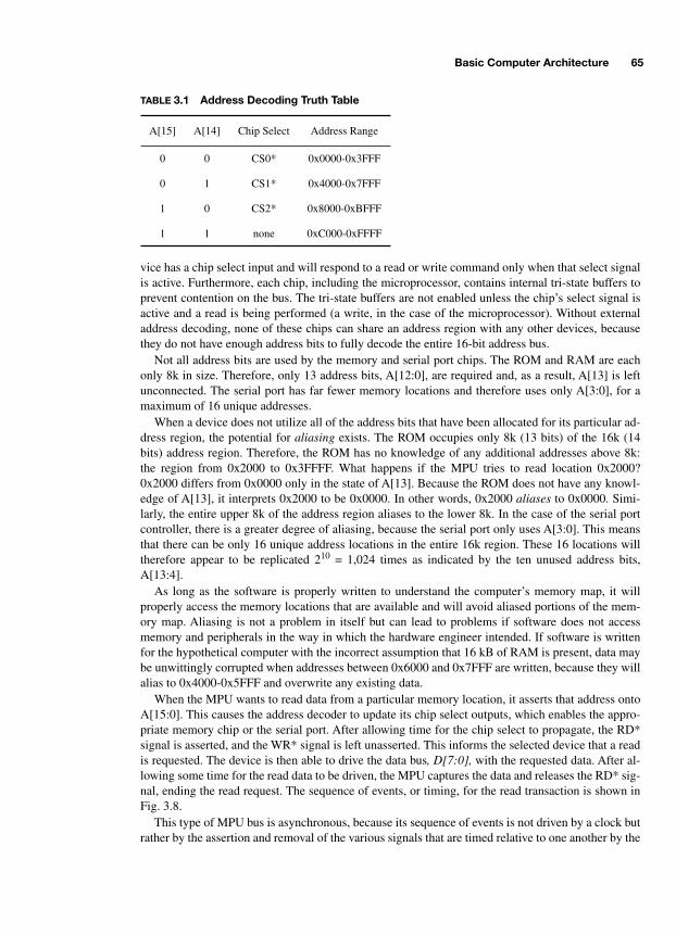
Basic Computer Architecture 65
vice has a chip select input and will respond to a read or write command only when that select signalis active. Furthermore, each chip, including the microprocessor, contains internal tri-state buffers toprevent contention on the bus. The tri-state buffers are not enabled unless the chip’s select signal isactive and a read is being performed (a write, in the case of the microprocessor). Without externaladdress decoding, none of these chips can share an address region with any other devices, becausethey do not have enough address bits to fully decode the entire 16-bit address bus.
Not all address bits are used by the memory and serial port chips. The ROM and RAM are eachonly 8k in size. Therefore, only 13 address bits, A[12:0], are required and, as a result, A[13] is leftunconnected. The serial port has far fewer memory locations and therefore uses only A[3:0], for amaximum of 16 unique addresses.
When a device does not utilize all of the address bits that have been allocated for its particular ad-dress region, the potential for
aliasing
exists. The ROM occupies only 8k (13 bits) of the 16k (14bits) address region. Therefore, the ROM has no knowledge of any additional addresses above 8k:the region from 0x2000 to 0x3FFFF. What happens if the MPU tries to read location 0x2000?0x2000 differs from 0x0000 only in the state of A[13]. Because the ROM does not have any knowl-edge of A[13], it interprets 0x2000 to be 0x0000. In other words, 0x2000
aliases
to 0x0000. Simi-larly, the entire upper 8k of the address region aliases to the lower 8k. In the case of the serial portcontroller, there is a greater degree of aliasing, because the serial port only uses A[3:0]. This meansthat there can be only 16 unique address locations in the entire 16k region. These 16 locations willtherefore appear to be replicated 2
10
= 1,024 times as indicated by the ten unused address bits,A[13:4].
As long as the software is properly written to understand the computer’s memory map, it willproperly access the memory locations that are available and will avoid aliased portions of the mem-ory map. Aliasing is not a problem in itself but can lead to problems if software does not accessmemory and peripherals in the way in which the hardware engineer intended. If software is writtenfor the hypothetical computer with the incorrect assumption that 16 kB of RAM is present, data maybe unwittingly corrupted when addresses between 0x6000 and 0x7FFF are written, because they willalias to 0x4000-0x5FFF and overwrite any existing data.
When the MPU wants to read data from a particular memory location, it asserts that address ontoA[15:0]. This causes the address decoder to update its chip select outputs, which enables the appro-priate memory chip or the serial port. After allowing time for the chip select to propagate, the RD*signal is asserted, and the WR* signal is left unasserted. This informs the selected device that a readis requested. The device is then able to drive the data bus
, D[7:0],
with the requested data. After al-lowing some time for the read data to be driven, the MPU captures the data and releases the RD* sig-nal, ending the read request. The sequence of events, or timing, for the read transaction is shown inFig. 3.8.
This type of MPU bus is asynchronous, because its sequence of events is not driven by a clock butrather by the assertion and removal of the various signals that are timed relative to one another by the
TABLE
3.1 Address Decoding Truth Table
A[15] A[14] Chip Select Address Range
0 0 CS0* 0x0000-0x3FFF
0 1 CS1* 0x4000-0x7FFF
1 0 CS2* 0x8000-0xBFFF
1 1 none 0xC000-0xFFFF
-Balch.book Page 65 Thursday, May 15, 2003 3:46 PM

66 Digital Fundamentals
MPU and the devices with which it is communicating. For this interface to work properly, the MPUmust allow enough time for the read to occur, regardless of the specific device with which it is com-municating. In other words, it must operate according to the capabilities of the slowest device—theleast common denominator.
Write timing is very similar, as seen in Fig. 3.9. Again, the MPU asserts the desired address ontoA[15:0], and the appropriate chip select is decoded. At the same time, the write data is driven ontoD[7:0]. Once the address and data have had time to stabilize, and after allowing time for the chip se-lect to propagate, the WR* enable signal is asserted to actually trigger the write. The WR* signal isde-asserted while data, address, and chip select are still stable so that there is no possibility of writ-ing to a different location and corrupting data. If the WR* signal is de-asserted at the same time asthe others, a race condition could develop wherein a particular device may sense the address (or dataor chip select) change just prior to WR* changing, resulting in a false write to another location or tothe current location with wrong data. Being an asynchronous interface, the duration of all signal as-sertions must be sufficient for all devices to properly execute the write.
An MPU interrupt signal is asserted by the serial port controller to enable easier programming ofthe serial port communication routine. Rather than having software continually poll the serial port tosee if data are waiting, the controller is configured to assert INTR* whenever a new byte arrives. TheMPU is then able to invoke an ISR, which can transfer the data byte from the serial port to the RAM.The interrupt also helps when transmitting data, because the speed of the typical serial port (often9,600 to 38,400 bps) is very slow as compared to the clock speed of even a slow MPU (1 to10 MHz). When the software wants to send a set of bytes out the serial port, it must send one byteand then wait a relatively long time until the serial port is ready for the next byte. Instead of pollingin a loop between bytes, the serial port controller asserts INTR* when it is time to send the nextbyte. The ISR can then respond with the next byte and return control to the main program that is run-
A[15:0]
CSx*
D[7:0]
RD*
valid
valid
Address asserted,read process begins
Address and RD* de-asserted,MPU accepts valid data
Chip select propagatesafter address valid
RD* asserted after allowingfor CSx* propagation delay
Device responds withdata after A, RD*, CSx*
Chip select propagatesafter address changes
Device returnsdata to tri-stateafter RD*, CSx*
de-assertion
FIGURE 3.8 MPU read timing.
A[15:0]
CSx*
D[7:0]
WR*
valid
valid
Address and
write data asserted
Address and write data
de-asserted together
Chip select propagates
after address valid
Chip select propagates
after address changesWR* asserted after address &
data valid and CSx* propagates
WR* de-asserted while
address, data still valid
FIGURE 3.9 MPU write timing.
-Balch.book Page 66 Thursday, May 15, 2003 3:46 PM

Basic Computer Architecture 67
ning at the time. Each time INTR* is asserted and the ISR responds, the ISR must be sure to clearthe interrupt condition in the serial port. Depending on the exact serial port device, a read or write toa specific register will clear the interrupt. If the interrupt is not cleared before the ISR issues a return-from-interrupt, the MPU may be falsely interrupted again for the same condition.
This computer contains two other functional elements: the clock and reset circuits. The 1-MHzclock must be supplied to the MPU continually for proper operation. In this example design, noother components in the computer require this clock. For fairly simple computers, this is a realisticscenario, because the buses and memory devices operate asynchronously. Many other computers,however, have synchronous buses, and the microprocessor clock must be distributed to other compo-nents in the system.
The reset circuit exists to start the MPU when the system is first turned on. Reset must be appliedfor a certain minimum duration after the power supply has stabilized. This is to ensure that the digi-tal circuits properly settle to known states before they are released from reset and allowed to beginnormal operation. As the computer is turned on, the reset circuit actively drives the RST* signal.Once power has stabilized, RST* is de-asserted and remains in this state indefinitely.
3.6 ADDRESS BANKING
A microprocessor’s address space is normally limited by the width of its address bus, but supple-mental logic can greatly expand address space, subject to certain limitations. Address banking is atechnique that increases the amount of memory a microprocessor can address. If an application re-quires 1 MB of RAM for storing large data structures, and an 8-bit microprocessor is used with a64-kB address space, address banking can enable the microprocessor to access the full 1 MB onesmall section at a time.
Address banking, also known as
paging
, takes a large quantity of memory, divides it into multiplesmaller banks, and makes each bank available to the microprocessor one at a time. A
bank addressregister
is maintained by the microprocessor and determines which bank of memory is selected atany given time. The selected bank is accessed through a portion of the microprocessor’s fixed ad-dress space, called a
window
, set aside for banked memory access. As shown in Fig. 3.10a, the upper16 kB of address space provides direct access to one of many 16-kB pages in the larger bankedmemory structure. Figure 3.10b shows the logical implementation of this banked memory scheme. A
16 kB BankAccessWindow
48 kB DirectMappedAddressSpace
(a)
8-bitMicroprocessor
4 MBBanked Memory
16 kB Page #255
16 kB Page #254
16 kB Page #1
16 kB Page #0
16 kB Page #2
8-bit BankAddress Register
Address DecodeLogic
A[15:0]
BA[7:0]
A[13:0]
A[15:14]
bankenable
(b)
FIGURE 3.10 Address banking.
-Balch.book Page 67 Thursday, May 15, 2003 3:46 PM

68 Digital Fundamentals
22-bit combined address is sent to the 4-MB banked memory structure: 256 pages
×
16 kB per page= 4 MB. These 22 bits are formed through the concatenation of the 8-bit bank address register and14 of the microprocessor’s low-order address bits, A[13:0]. The eight bank-address bits are changedinfrequently whenever the microprocessor is ready for a new page in memory. The 14 microproces-sor-address bits can change each time the window is accessed.
The details of a banking scheme can be modified according to the application’s requirements. Thebank access window can be increased or decreased, and more or fewer pages can be defined. If anapplication operates on many small sets of data, a larger number of smaller pages may be suitable. Ifthe data or software set is widely dispersed, it may be better to increase the window size as much aspossible to minimize the bank address register update rate.
While address banking can greatly increase the memory available to a microprocessor, it does sowith the penalties of increased access time on page switches and more complexity in managing thesegmented address space. Each time the microprocessor wants to access a location in a differentpage, it must update the bank address register. This penalty is acceptable in some applications. How-ever, if the application requires both consistently fast access time and large memory size, a faster,more expensive microprocessor may be required that suits these needs.
The complexity of managing the segmented address space dissuades some engineers from em-ploying address banking. Software usually bears the brunt of recognizing when necessary data re-sides in a different page and then updating the bank address register to access that page. It is easierfor software to deal with a large, continuous address space. With the easy availability and low cost of32-bit microprocessors, address banking is not as common as it used to be. However, if an 8-bit mi-croprocessor must be used for cost reduction or other limitations, address banking may be usefulwhen memory demands increase beyond 64 kB.
3.7 DIRECT MEMORY ACCESS
Transferring data from one region of memory to another is a common task performed within a com-puter. Incoming data may be transferred from a serial communications controller into memory, andoutgoing data may be transferred from memory to the controller. Memory-to-memory transfers arecommon, too, as data structures are moved between subprograms, each of which may have separateregions of memory set aside for its private use. The speed with which memory is transferred nor-mally depends on the time that the microprocessor takes to perform successive read and write opera-tions. Each byte transferred requires several microprocessor operations: load accumulator, storeaccumulator, update address for next byte, and check if there is more data. Instead of simply movinga stream of bytes without interruption, the microprocessor is occupied mostly by the overhead ofcalculating new addresses and checking to see if more data is waiting. Computers that perform ahigh volume of memory transfers may exhibit performance bottlenecks as a result of the overhead ofhaving the microprocessor spend too much of its time reading and writing memory.
Memory transfer performance can be improved using a technique called
direct memory access
, orDMA. DMA logic intercedes at the microprocessor’s request to directly move data between a sourceand destination. A
DMA controller
(DMAC) sits on the microprocessor bus and contains logic that isspecifically designed to rapidly move data without the overhead of simultaneously fetching and de-coding instructions. When the microprocessor determines that a block of data is ready to move, itprograms the DMAC with the starting address of the source data, the number of bytes to move, andthe starting address of the destination data. When the DMAC is triggered, the microprocessor tem-porarily relinquishes control of its bus so the DMAC can take over and quickly move the data. TheDMAC serves as a surrogate processor by directly generating addresses and reading and writingdata. From the microprocessor bus perspective, nothing has changed, and data transfers proceed nor-
-Balch.book Page 68 Thursday, May 15, 2003 3:46 PM

Basic Computer Architecture 69
mally despite being controlled by the DMAC rather than the microprocessor. Figure 3.11 shows thebasic internal structure of a DMAC.
A DMA transfer can be initiated by either the microprocessor or an I/O device that contains logicto assert a request to the DMAC. DMA transfers are generally broken into two categories: periph-eral/memory and memory/memory. Peripheral/memory transfers move data to a peripheral or re-trieve data from a peripheral. A peripheral/memory transfer can be triggered by a DMA-aware I/O-device when it is ready to accept more outgoing data or incoming data has arrived. These are called
single-address transfers,
because the DMAC typically controls only a single address—that of thememory side of the transfer. The peripheral address is typically a fixed offset into its register set andis asserted by supporting control logic that assists in the connectivity between the peripheral and theDMAC.
DMA transfers do not have to be continuous, and they are often not in the case of a peripheraltransfer. If the microprocessor sets up a DMA transfer from a serial communications controller tomemory, it programs the DMAC to write a certain quantity of data into memory. However, the trans-fer does not begin until the serial controller asserts a DMA request indicating that data is ready.When this request occurs, the DMAC arbitrates for access to the microprocessor bus by asserting abus request. Some time later, the microprocessor or its support logic will grant the bus to the DMACand temporarily pause the microprocessor’s bus activity. The DMAC can then transfer a single unitof data from the serial controller into memory. The unit of data transfer may be any number of bytes.When finished, the DMAC relinquishes control of the bus back to the microprocessor.
Memory/memory transfers move data from one region in memory to another. These are called
dual-address transfers,
because the DMAC controls two addresses into memory—source and desti-nation. Memory/memory transfers are triggered by the microprocessor and can execute continu-ously, because the data block to be moved is ready and waiting in memory.
Even when DMA transfers execute one byte at a time, they are still more efficient than the micro-processor, because the DMAC is capable of transferring a byte or word (per the microprocessor’sdata bus width) in a single bus cycle rather than the microprocessor’s load/store mechanism with ad-ditional overhead. There is some initial overhead in setting up the DMA transfer, so it is not efficientto use DMA for very short transfers. If the microprocessor needs to move only a few bytes, it shouldprobably do so on its own. However, the DMAC initialization overhead is more than compensatedfor if dozens or hundreds of bytes are being moved.
Source AddressRegister
Transfer LengthRegister
DestinationAddress Register
Control Registers DMATransfer
Logic
Bus ControlLogic
address bus
data bus
DMA request/acknowledge
bus request/grant
FIGURE 3.11 DMA controller block diagram.
-Balch.book Page 69 Thursday, May 15, 2003 3:46 PM

70 Digital Fundamentals
A typical DMAC supports multiple channels,
each of which controls a different DMA transfer.While only one transfer can execute at any given moment, multiple transfers can be interleaved toprevent one peripheral from being starved for data while another is being serviced. Because a typicalperipheral transfer is not continuous, each DMA channel can be assigned to each active peripheral.A DMAC can have one channel configured to load incoming data from a serial controller, another tostore data to a disk drive controller, and a third to move data from one region of memory to another.Once initialized by the microprocessor, the exact order and interleaving of multiple channels is re-solved by the individual DMA request signals, and any priority information is stored in the DMAC.
When a DMAC channel has completed transferring the requested quantity of data, the DMAC as-serts an interrupt to the microprocessor to signal that the data has been moved. At this point, the mi-croprocessor can restart a new DMA transfer if desired and invoke any necessary routines to processdata that has been moved.
External DMA support logic may be necessary, depending on the specific DMAC, microproces-sor, and peripherals that are being used. Some microprocessors contain built-in DMAC arbitrationlogic. Some peripherals contain built-in DMA request logic, because they are specifically designedfor these high-efficiency memory transfers. Custom arbitration logic typically functions by waitingfor the DMAC to request the bus and then pausing the microprocessor’s bus transfers until theDMAC relinquishes the bus. This pause operation is performed according to the specifications of theparticular microprocessor. Custom peripheral control logic can include DMAC read/write interfacelogic to assert the correct peripheral address when a transfer begins and perform any other requiredmapping between the DMAC’s transfer enable signaling and the peripheral’s read/write interface.
3.8 EXTENDING THE MICROPROCESSOR BUS
A microprocessor bus is intended to directly connect to memory and I/O devices that are in closeproximity to the microprocessor. As such, its electrical and functional properties are suited for rela-tively short interconnecting wires and relatively simple device interfaces that respond with data soonafter the microprocessor issues a request. Many computers, however, require some mechanism to ex-tend the microprocessor bus so that additional hardware, such as plug-in expansion cards or memorymodules, can enhance the system with new capabilities. Supporting these modular extensions to thecomputer’s architecture can be relatively simple or quite complex, depending on the required degreeof expandability and the physical distances across which data must be communicated.
Expansion buses are generally broken into two categories, memory and I/O, because thesegroups’ respective characteristics are usually quite different. General-purpose memory is a high-bandwidth resource to which the microprocessor requires immediate access so that it can maintain ahigh level of throughput. Memory is also a predictable and regular structure, both logically andphysically. If more RAM is added to a computer, it is fairly certain that some known number ofchips will be required for a given quantity of memory. In contrast, I/O by nature is very diverse, andits bandwidth requirements are usually lower than that of memory. I/O expansion usually involvescards of differing complexity and architecture as a result of the wide range of interfaces that can besupported (e.g., disk drive controller versus serial port controller). Therefore, an I/O expansion busmust be flexible enough to interface with a varying set of modules, some of which may not havebeen conceived of when the computer is first designed.
Memory expansion buses are sometimes direct extensions of the microprocessor bus. From thepreceding 8-bit computer example, the upper 16 kB of memory could be reserved for future expan-sion. A provision for future expansion could be as simple as adding a connector or socket for an ex-tra memory chip. In this case, no special augmentation of the microprocessor bus is required.However, in a larger system with more address space, provisions must be made for more than one
-Balch.book Page 70 Thursday, May 15, 2003 3:46 PM

Basic Computer Architecture 71
additional memory chip. In these situations, a simple buffered extension of the microprocessor busmay suffice. A buffer, in this context, is an IC that passes data from one set of pins to another,thereby electrically separating two sections of a bus. As shown in Fig. 3.12, a buffer can extend a mi-croprocessor bus so that its logical functionality remains unchanged, but its electrical characteristicsare enhanced to provide connectivity across a greater distance (to a multichip memory expansionmodule). A unidirectional address buffer extends the address bus from the microprocessor to expan-sion memory devices. A bidirectional data buffer extends the bus away from the microprocessor onwrites and toward the microprocessor on reads. The direction of the data buffer is controlled accord-ing to the state of read/write enable signals generated by the microprocessor.
More complex memory structures may contain dedicated memory control logic that sits betweenthe microprocessor and the actual memory devices. Expanding such a memory architecture is gener-ally accomplished by augmenting the “back-side” memory device bus as shown in Fig. 3.13 ratherthan by adding additional controllers onto an extended microprocessor bus. Such an expansionscheme may or may not require buffers, depending on the electrical characteristics of the bus inquestion.
I/O buses may also be direct extensions of the microprocessor bus. The original expansion bus inthe IBM PC, developed in the early 1980s, is essentially an extended Intel 8088 microprocessor busthat came to be known as the Industry Standard Architecture (ISA) bus. Each I/O card on the ISAbus is mapped in a unique address range in the microprocessor’s memory. Therefore, when softwarewants to read or write a register on an I/O card, it simply performs an access to the desired location.The ISA bus added a few features beyond the raw 8088 bus, including DMA and variable wait statesfor slow I/O devices. A wait state results when a device cannot immediately respond to the micro-processor’s request and asserts a signal to stretch the access so that it can respond properly.
Microprocessor
LocalMemory
A[15:0]
D[7:0]
ExpansionMemory
FIGURE 3.12 Buffered microprocessor bus for memory expansion.
Microprocessor
Local Address/Local
MemoryExpansionMemory
MemoryController
Memory Bus optional buffer
Data Bus
FIGURE 3.13 Extended memory controller bus.
-Balch.book Page 71 Thursday, May 15, 2003 3:46 PM
72 Digital Fundamentals
Direct extensions such as the ISA bus are fairly easy to implement and serve well in applicationswhere I/O response time does not unduly restrict microprocessor throughput. As computers havegotten faster, the throughput of microprocessors has rapidly outstripped the response times of all butthe fastest I/O devices. In comparison to a modern microprocessor, a hard-disk controller is ratherslow, with response times measured in microseconds rather than nanoseconds. Additionally, as bussignals become faster, the permissible length of interconnecting wires decreases, limiting their ex-pandability. These and other characteristics motivate the decoupling of the microprocessor’s localbus from the computer’s I/O bus.
An I/O bus can be decoupled from the microprocessor bus by inserting an intermediate bus con-troller between them that serves as an interface, or translator, between the two buses. Once the busesare separated, activity on one bus does not necessarily obstruct activity on the other. If the micropro-cessor wants to write a block of data to a slow device, it can rapidly transfer that data to the bus con-troller and then continue with other operations at full speed while the controller slowly transfers thedata to the I/O device. This mechanism is called a posted-write, because the bus controller allows themicroprocessor to complete, or post, its write before the write actually completes. Separate busesalso open up the possibility of multiple microprocessors or logic elements performing I/O operationswithout conflicting with the central microprocessor. In a multimaster system, a specialized DMAcontroller can transfer data between two peripherals such as disk controllers while the microproces-sor goes about its normal business.
The Peripheral Component Interconnect (PCI) bus is the industry-standard follow-on to the ISAbus, and it implements such advanced features as posted-writes, multiple-masters, and multiple bussegments. Each PCI bus segment is separated from the others via a PCI bridge chip. Only traffic thatmust travel between buses crosses a bridge, thereby reducing congestion on individual PCI bus seg-ments. One segment can be involved in a data transfer between two devices without affecting a si-multaneous transfer between two other devices on a different segment. These performance-enhancing features do not come for free, however. Their cost is manifested by the need for dedicatedPCI control logic in bridge chips and in the I/O devices themselves. It is generally simpler to imple-ment an I/O device that is directly mapped into the microprocessor’s memory space, but the overallperformance of the computer may suffer under demanding applications.
3.9 ASSEMBLY LANGUAGE AND ADDRESSING MODES
With the hardware ready, a computer requires software to make it more than an inactive collection ofcomponents. Microprocessors fetch instructions from program memory, each consisting of an op-code and, optionally, additional operands following the opcode. These opcodes are binary data thatare easy for the microprocessor to decode, but they are not very readable by a person. To enable aprogrammer to more easily write software, an instruction representation called assembly languagewas developed. Assembly language is a low-level language that directly represents each binary op-code with a human-readable text mnemonic. For example, the mnemonic for an unconditionalbranch-to-subroutine instruction could be BSR. In contrast, a high-level language such as C++ orJava contains more complex logical expressions that may be automatically converted by a compilerto dozens of microprocessor instructions. Assembly language programs are assembled, rather thancompiled, into opcodes by directly translating each mnemonic into its binary equivalent.
Assembly language also makes programming easier by enabling the usage of text labels in placeof hard-coded addresses. A subroutine can be named FOO, and when BSR FOO is encountered bythe assembler, a suitable branch target address will be automatically calculated in place of the labelFOO. Each type of assembler requires a slightly different format and syntax, but there are general as-sembly language conventions that enable a programmer to quickly adapt to specific implementations
-Balch.book Page 72 Thursday, May 15, 2003 3:46 PM
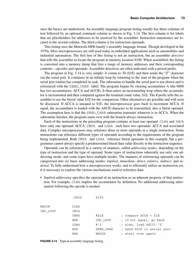
Basic Computer Architecture 73
once the basics are understood. An assembly language program listing usually has three columns oftext followed by an optional comment column as shown in Fig. 3.14. The first column is for labelsthat are placeholders for addresses to be resolved by the assembler. Instruction mnemonics are lo-cated in the second column. The third column is for instruction operands.
This listing uses the Motorola 6800 family’s assembly language format. Though developed in the1970s, 68xx microprocessors are still used today in embedded applications such as automobiles andindustrial automation. The first line of this listing is not an instruction, but an assembler directivethat tells the assembler to locate the program at memory location $100. When assembled, the listingis converted into a memory dump that lists a range of memory addresses and their correspondingcontents—opcodes and operands. Assembler directives are often indicated with a period prefix.
The program in Fig. 3.14 is very simple: it counts to 30 ($1E) and then sends the “Z” characterout the serial port. It continues in an infinite loop by returning to the start of the program when theserial port routine has completed its task. The subroutine to handle the serial port is not shown and isreferenced with the SEND_CHAR label. The program begins by clearing accumulator A (the 6800has two accumulators: ACCA and ACCB). It then enters an incrementing loop where the accumula-tor is incremented and then compared against the terminal count value, $1E. The # prefix tells the as-sembler to use the literal value $1E for the comparison. Other alternatives are possible and will soonbe discussed. If ACCA is unequal to $1E, the microprocessor goes back to increment ACCA. Ifequal, the accumulator is loaded with the ASCII character to be transmitted, also a literal operand.The assumption here is that the SEND_CHAR subroutine transmits whatever is in ACCA. When thesubroutine finishes, the program starts over with the branch-always instruction.
Each of the instructions in the preceding program contains at least one operand. CLRA and INCAhave only one operand: ACCA. CMPA and LDAA each have two operands: ACCA and associateddata. Complex microprocessors may reference three or more operands in a single instruction. Someinstructions can reference different types of operands according to the requirements of the programbeing implemented. Both CMPA and LDAA reference literal operands in this example, but a pro-grammer cannot always specify a predetermined literal data value directly in the instruction sequence.
Operands can be referenced in a variety of manners, called addressing modes, depending on thetype of instruction and the type of operand. Some types of instructions inherently use only one ad-dressing mode, and some types have multiple modes. The manners of referencing operands can becategorized into six basic addressing modes: implied, immediate, direct, relative, indirect, and in-dexed. To fully understand how a microprocessor works, and to efficiently utilize an instruction set,it is necessary to explore the various mechanisms used to reference data.
• Implied addressing specifies the operand of an instruction as an inherent property of that instruc-tion. For example, CLRA implies the accumulator by definition. No additional addressing infor-mation following the opcode is needed.
.ORIG $100
BEGIN CLRA
INC_LOOP INCA
CMPA #$1E ; compare ACCA = $1E
BNE INC_LOOP ; if not equal, go back
LDAA #'Z' ; else, load ASCII 'Z'
BSR SEND_CHAR ; send ACCA to serial port
BRA BEGIN ; start over again
FIGURE 3.14 Typical assembly language listing.
-Balch.book Page 73 Thursday, May 15, 2003 3:46 PM

74 Digital Fundamentals
• Immediate addressing places an operand’s value literally into the instruction sequence. LDAA#’Z’ has its primary operand immediately available following the opcode. An immediate oper-and is indicated with the # prefix in some assembly languages. Eight-bit microprocessors witheight-bit instruction words cannot fit an immediate value into the instruction word itself and,therefore, require that an extra byte following the opcode be used to specify the immediate value.More powerful 32-bit microprocessors can often fit a 16-bit or 24-bit immediate value within theinstruction word. This saves an additional memory fetch to obtain the operand.
Direct addressing places the address of an operand directly into the instruction sequence. Insteadof specifying LDAA #’Z’, the programmer could specify LDAA $1234. This version of the in-struction would tell the microprocessor to read memory location $1234 and load the resultingvalue into the accumulator. The operand is directly available by looking into the memory addressspecified just following the instruction. Direct addressing is useful when there is a need to read afixed memory location. Usage of the direct addressing mode has a slightly different impact on var-ious microprocessors. A typical 8-bit microprocessor has a 16-bit address space, meaning that twobytes following the opcode are necessary to represent a direct address. The 8-bit microprocessorwill have to perform two additional 8-bit fetch operations to load the direct address. A typical 32-bit microprocessor has a 32-bit address space, meaning that 4 bytes following the opcode are nec-essary. If the 32-bit microprocessor has a 32-bit data bus, only one additional 32-bit fetch opera-tion is required to load the direct address.
Relative addressing places an operand’s relative address into the instruction sequence. A relativeaddress is expressed as a signed offset relative to the current value of the PC. Relative addressingis often used by branch instructions, because the target of a branch is usually within a short dis-tance of the PC, or current instruction. For example, BNE INC_LOOP results in a branch-if-not-equal backward by two instructions. The assembler automatically resolves the addresses and cal-culates a relative offset to be placed following the BNE opcode. This relative operation is per-formed by adding the offset to the PC. The new PC value is then used to resume the instructionfetch and execution process. Relative addressing can utilize both positive and negative deltas thatare applied to the PC. A microprocessor’s instruction format constrains the relative range that canbe specified in this addressing mode. For example, most 8-bit microprocessors provide only an 8-bit signed field for relative branches, indicating a range of +127/–128 bytes. The relative deltavalue is stored into its own byte just after the opcode. Many 32-bit microprocessors allow a 16-bitdelta field and are able to fit this value into the 32-bit instruction word, enabling the entire instruc-tion to be fetched in a single memory read. Limiting the range of a relative operation is generallynot an excessive constraint because of software’s locality property. Locality in this context meansthat the set of instructions involved in performing a specific task are generally relatively close to-gether in memory. The locality property covers the great majority of branch instructions. Forthose few branches that have their targets outside of the allowed relative range, it is necessary toperform a short relative branch to a long jump instruction that specifies a direct address. This re-duces the efficiency of the microprocessor by having to perform two branches when only one isideally desired, but the overall efficiency of saving extra memory accesses for the majority ofshort branches is worth the trade-off.
• Indirect addressing specifies an operand’s direct address as a value contained in another register.The other register becomes a pointer to the desired data. For example, a microprocessor with twoaccumulators can load ACCA with the value that is at the address in ACCB. LDAA (ACCB)would tell the microprocessor to put the value of accumulator B onto the address bus, perform aread, and put the returned value into accumulator A. Indirect addressing allows writing softwareroutines that operate on data at different addresses. If a programmer wants to read or write an arbi-
-Balch.book Page 74 Thursday, May 15, 2003 3:46 PM
Basic Computer Architecture 75
trary entry in a data table, the software can load the address of that entry into a microprocessorregister and then perform an indirect access using that register as a pointer. Some microprocessorsplace constraints on which registers can be used as references for indirect addressing. In the caseof a 6800 microprocessor, LDAA (ACCB) is not actually a supported operation but serves as asyntactical example for purposes of discussion.
• Indexed addressing is a close relative (no pun intended) of indirect addressing, because it also re-fers to an address contained in another register. However, indexed addressing also specifies an off-set, or index, to be added to that register base value to generate the final operand address: base +offset = final address. Some microprocessors allow general accumulator registers to be used asbase-address registers, but others, such as the 6800, provide special index registers for this pur-pose. In many 8-bit microprocessors, a full 16-bit address cannot be obtained from an 8-bit accu-mulator serving as the base address. Therefore, one or more separate index registers are presentfor the purpose of indexed addressing. In contrast, many 32-bit microprocessors are able to spec-ify a full 32-bit address with any general-purpose register and place no limitations on which regis-ter serves as the index register. Indexed addressing builds upon the capabilities of indirectaddressing by enabling multiple address offsets to be referenced from the same base address.LDAA (X+$20) would tell the microprocessor to add $20 to the index register, X, and use theresulting address to fetch data to be loaded into ACCA. One simple example of using indexed ad-dressing is a subroutine to add a set of four numbers located at an arbitrary location in memory.Before calling the subroutine, the main program can set an index register to point to the table ofnumbers. Within the subroutine, four individual addition instructions use the indexed addressingmode to add the locations X+0, X+1, X+2, and X+3. When so written, the subroutine is flexibleenough to be used for any such set of numbers. Because of the similarity of indexed and indirectaddressing, some microprocessors merge them into a single mode and obtain indirect addressingby performing indexed addressing with an index value of zero.
The six conceptual addressing modes discussed above represent the various logical mechanismsthat a microprocessor can employ to access data. It is important to realize that each individual micro-processor applies these addressing modes differently. Some combine multiple modes into a singlemode (e.g., indexed and indirect), and some will create multiple submodes out of a single mode. Theexact variation depends on the specifics of an individual microprocessor’s architecture.
With the various addressing modes modifying the specific opcode and operands that are presentedto the microprocessor, the benefits of using assembly language over direct binary values can be ob-served. The programmer does not have to worry about calculating branch target addresses or resolv-ing different addressing modes. Each mnemonic can map to several unique opcodes, depending onthe addressing mode used. For example, the LDAA instruction in Fig. 3.14 could easily have used ex-tended addressing by specifying a full 16-bit address at which the ASCII transmit-value is located.Extended addressing is the 6800’s mechanism for specifying a 16-bit direct address. (The 6800’s di-rect addressing involves only an eight-bit address.) In either case, the assembler would determine thecorrect opcode to represent LDAA and insert the correct binary values into the memory dump. Addi-tionally, because labels are resolved each time the program is assembled, small changes to the pro-gram can be made that add or remove instructions and labels, and the assembler will automaticallyadjust the resulting addresses accordingly.
Programming in assembly language is different from using a high-level language, because onemust think in smaller steps and have direct knowledge about the microprocessor’s operation and ar-chitecture. Assembly language is processor-specific instead of generic, as with a high-level lan-guage. Therefore, assembly language programming is usually restricted to special cases such as bootcode or routines in which absolute efficiency and performance are demanded. A human programmerwill usually be able to write more efficient assembly language than a high-level language compiler
-Balch.book Page 75 Thursday, May 15, 2003 3:46 PM

76 Digital Fundamentals
can generate. In large programs, the slight inefficiency of the compiler is well worth the trade-off forease of programming in a high-level language. However, time-critical routines such as I/O drivers orISRs may benefit from manual assembly language coding.
-Balch.book Page 76 Thursday, May 15, 2003 3:46 PM

77
CHAPTER 4
Memory
Memory is as fundamental to computer architecture as any other element. The ability of a system’smemory to transact the right quantity of data in the right span of time has a substantial impact onhow that system fulfills its design goals. Digital engineers struggle with innovative ways to improvememory density and bandwidth in a way that is tailored to a specific application’s performance andcost constraints.
Knowledge of prevailing memory technologies’ strengths and weaknesses is a key requirement fordesigning digital systems. When memory architecture is chosen that complements the rest of the sys-tem, a successful design moves much closer to fruition. Conversely, inappropriate memory architecturecan doom a good idea to the engineering doldrums of impracticality brought on by artificial complexity.
This chapter provides an introduction to various solid-state memory technologies and explainshow they work from an internal structural perspective as well as an interface timing perspective. Amemory’s internal structure is important to an engineer, because it explains why that memory mightbe more suited for one application over another. Interface timing is where the rubber meets the road,because it defines how other elements in the system can access memory components’ contents. Thewrong interface on a memory chip can make it difficult for external logic such as a microprocessorto access that memory and still have time left over to perform the necessary processing on that data.
Basic memory organization and terminology are introduced first. This is followed by a discussionof the prevailing read-only memory technologies: EPROM, flash, and EEPROM. AsynchronousSRAM and DRAM technologies, the foundations for practically all random-access memories, arepresented next. These asynchronous RAMs are no longer on the forefront of memory technology butstill find use in many systems. Understanding their operation not only enables their application, italso contributes to an understanding of the most recent synchronous RAM technologies. (High-per-formance synchronous memories are discussed later in the book.) The chapter concludes with a dis-cussion of two types of specialty memories: multiport RAMs and FIFOs. Multiport RAMs andFIFOs are found in many applications where memory serves less as a storage element and more as acommunications channel between distinct logic blocks.
4.1 MEMORY CLASSIFICATIONS
Microprocessors require memory resources in which to store programs and data. Memory can beclassified into two broad categories: volatile and nonvolatile. Volatile memory loses its contentswhen power is turned off. Nonvolatile memory retains its contents indefinitely, even when there is nopower present. Nonvolatile memory can be used to hold the boot code for a computer so that the mi-croprocessor can have a place to get started. Once the computer begins initializing itself from non-volatile memory, volatile memory is used to store dynamic variables, including the stack and otherprograms that may be loaded from a disk drive. Figure 4.1 shows that a general memory device con-sists of a bit-storage array, address-decode logic, input/output logic, and control logic.
-Balch.book Page 77 Thursday, May 15, 2003 3:46 PM
Copyright 2003 by The McGraw-Hill Companies, Inc. Click Here for Terms of Use.
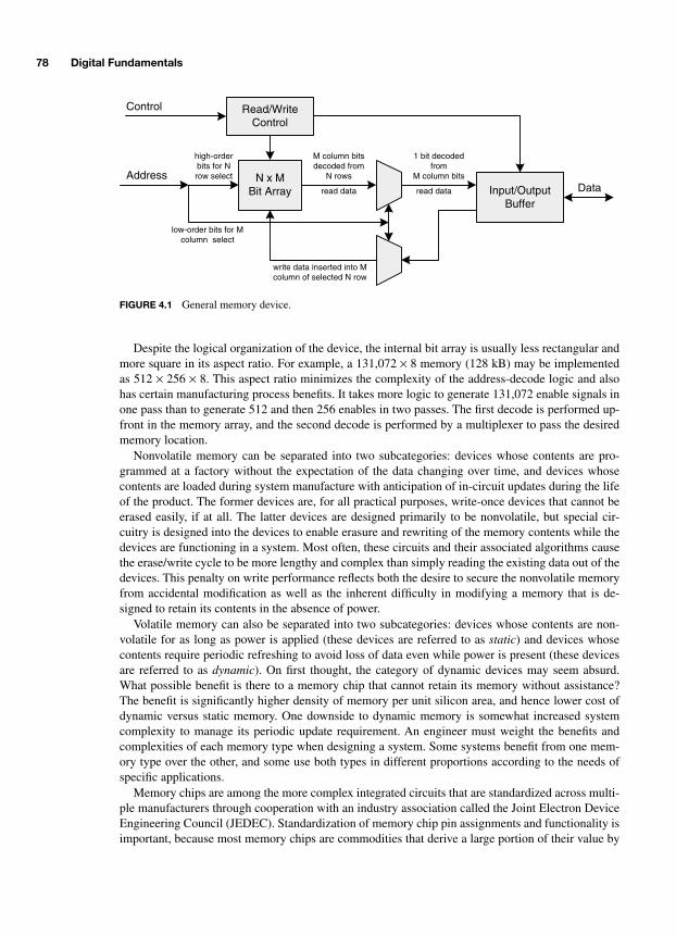
78 Digital Fundamentals
Despite the logical organization of the device, the internal bit array is usually less rectangular andmore square in its aspect ratio. For example, a 131,072
×
8 memory (128 kB) may be implementedas 512
×
256
×
8. This aspect ratio minimizes the complexity of the address-decode logic and alsohas certain manufacturing process benefits. It takes more logic to generate 131,072 enable signals inone pass than to generate 512 and then 256 enables in two passes. The first decode is performed up-front in the memory array, and the second decode is performed by a multiplexer to pass the desiredmemory location.
Nonvolatile memory can be separated into two subcategories: devices whose contents are pro-grammed at a factory without the expectation of the data changing over time, and devices whosecontents are loaded during system manufacture with anticipation of in-circuit updates during the lifeof the product. The former devices are, for all practical purposes, write-once devices that cannot beerased easily, if at all. The latter devices are designed primarily to be nonvolatile, but special cir-cuitry is designed into the devices to enable erasure and rewriting of the memory contents while thedevices are functioning in a system. Most often, these circuits and their associated algorithms causethe erase/write cycle to be more lengthy and complex than simply reading the existing data out of thedevices. This penalty on write performance reflects both the desire to secure the nonvolatile memoryfrom accidental modification as well as the inherent difficulty in modifying a memory that is de-signed to retain its contents in the absence of power.
Volatile memory can also be separated into two subcategories: devices whose contents are non-volatile for as long as power is applied (these devices are referred to as
static
) and devices whosecontents require periodic refreshing to avoid loss of data even while power is present (these devicesare referred to as
dynamic
). On first thought, the category of dynamic devices may seem absurd.What possible benefit is there to a memory chip that cannot retain its memory without assistance?The benefit is significantly higher density of memory per unit silicon area, and hence lower cost ofdynamic versus static memory. One downside to dynamic memory is somewhat increased systemcomplexity to manage its periodic update requirement. An engineer must weight the benefits andcomplexities of each memory type when designing a system. Some systems benefit from one mem-ory type over the other, and some use both types in different proportions according to the needs ofspecific applications.
Memory chips are among the more complex integrated circuits that are standardized across multi-ple manufacturers through cooperation with an industry association called the Joint Electron DeviceEngineering Council (JEDEC). Standardization of memory chip pin assignments and functionality isimportant, because most memory chips are commodities that derive a large portion of their value by
N x MBit Array Input/Output
Buffer
AddressData
Read/WriteControl
Control
M column bitsdecoded from
N rows
1 bit decodedfrom
M column bits
read data read data
write data inserted into Mcolumn of selected N row
high-orderbits for Nrow select
low-order bits for Mcolumn select
FIGURE 4.1 General memory device.
-Balch.book Page 78 Thursday, May 15, 2003 3:46 PM
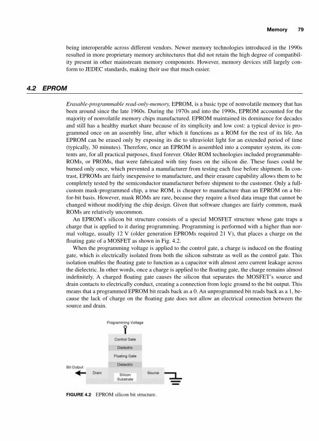
Memory 79
being interoperable across different vendors. Newer memory technologies introduced in the 1990sresulted in more proprietary memory architectures that did not retain the high degree of compatibil-ity present in other mainstream memory components. However, memory devices still largely con-form to JEDEC standards, making their use that much easier.
4.2 EPROM
Erasable-programmable read-only-memory,
EPROM, is a basic type of nonvolatile memory that hasbeen around since the late 1960s. During the 1970s and into the 1990s, EPROM accounted for themajority of nonvolatile memory chips manufactured. EPROM maintained its dominance for decadesand still has a healthy market share because of its simplicity and low cost: a typical device is pro-grammed once on an assembly line, after which it functions as a ROM for the rest of its life. AnEPROM can be erased only by exposing its die to ultraviolet light for an extended period of time(typically, 30 minutes). Therefore, once an EPROM is assembled into a computer system, its con-tents are, for all practical purposes, fixed forever. Older ROM technologies included programmable-ROMs, or PROMs, that were fabricated with tiny fuses on the silicon die. These fuses could beburned only once, which prevented a manufacturer from testing each fuse before shipment. In con-trast, EPROMs are fairly inexpensive to manufacture, and their erasure capability allows them to becompletely tested by the semiconductor manufacturer before shipment to the customer. Only a full-custom mask-programmed chip, a true ROM, is cheaper to manufacture than an EPROM on a bit-for-bit basis. However, mask ROMs are rare, because they require a fixed data image that cannot bechanged without modifying the chip design. Given that software changes are fairly common, maskROMs are relatively uncommon.
An EPROM’s silicon bit structure consists of a special MOSFET structure whose gate traps acharge that is applied to it during programming. Programming is performed with a higher than nor-mal voltage, usually 12 V (older generation EPROMs required 21 V), that places a charge on thefloating gate of a MOSFET as shown in Fig. 4.2.
When the programming voltage is applied to the control gate, a charge is induced on the floatinggate, which is electrically isolated from both the silicon substrate as well as the control gate. Thisisolation enables the floating gate to function as a capacitor with almost zero current leakage acrossthe dielectric. In other words, once a charge is applied to the floating gate, the charge remains almostindefinitely. A charged floating gate causes the silicon that separates the MOSFET’s source anddrain contacts to electrically conduct, creating a connection from logic ground to the bit output. Thismeans that a programmed EPROM bit reads back as a 0. An unprogrammed bit reads back as a 1, be-cause the lack of charge on the floating gate does not allow an electrical connection between thesource and drain.
FIGURE 4.2 EPROM silicon bit structure.
-Balch.book Page 79 Thursday, May 15, 2003 3:46 PM
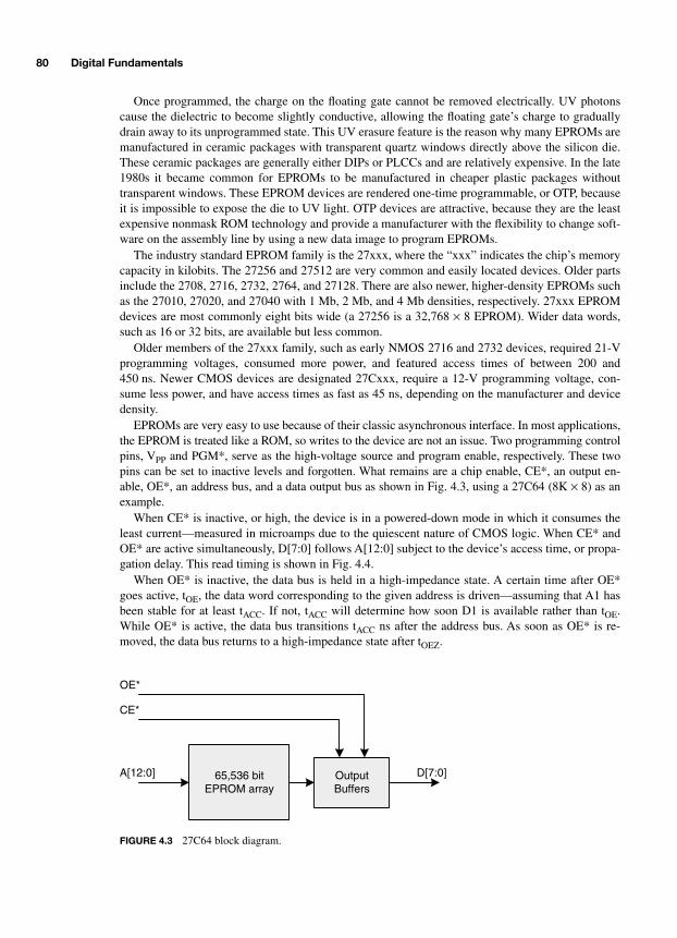
80 Digital Fundamentals
Once programmed, the charge on the floating gate cannot be removed electrically. UV photonscause the dielectric to become slightly conductive, allowing the floating gate’s charge to graduallydrain away to its unprogrammed state. This UV erasure feature is the reason why many EPROMs aremanufactured in ceramic packages with transparent quartz windows directly above the silicon die.These ceramic packages are generally either DIPs or PLCCs and are relatively expensive. In the late1980s it became common for EPROMs to be manufactured in cheaper plastic packages withouttransparent windows. These EPROM devices are rendered one-time programmable, or OTP, becauseit is impossible to expose the die to UV light. OTP devices are attractive, because they are the leastexpensive nonmask ROM technology and provide a manufacturer with the flexibility to change soft-ware on the assembly line by using a new data image to program EPROMs.
The industry standard EPROM family is the 27xxx, where the “xxx” indicates the chip’s memorycapacity in kilobits. The 27256 and 27512 are very common and easily located devices. Older partsinclude the 2708, 2716, 2732, 2764, and 27128. There are also newer, higher-density EPROMs suchas the 27010, 27020, and 27040 with 1 Mb, 2 Mb, and 4 Mb densities, respectively. 27xxx EPROMdevices are most commonly eight bits wide (a 27256 is a 32,768
×
8 EPROM). Wider data words,such as 16 or 32 bits, are available but less common.
Older members of the 27xxx family, such as early NMOS 2716 and 2732 devices, required 21-Vprogramming voltages, consumed more power, and featured access times of between 200 and450 ns. Newer CMOS devices are designated 27Cxxx, require a 12-V programming voltage, con-sume less power, and have access times as fast as 45 ns, depending on the manufacturer and devicedensity.
EPROMs are very easy to use because of their classic asynchronous interface. In most applications,the EPROM is treated like a ROM, so writes to the device are not an issue. Two programming controlpins, V
PP
and PGM*, serve as the high-voltage source and program enable, respectively. These twopins can be set to inactive levels and forgotten. What remains are a chip enable, CE*, an output en-able, OE*, an address bus, and a data output bus as shown in Fig. 4.3, using a 27C64 (8K
×
8) as anexample.
When CE* is inactive, or high, the device is in a powered-down mode in which it consumes theleast current—measured in microamps due to the quiescent nature of CMOS logic. When CE* andOE* are active simultaneously, D[7:0] follows A[12:0] subject to the device’s access time, or propa-gation delay. This read timing is shown in Fig. 4.4.
When OE* is inactive, the data bus is held in a high-impedance state. A certain time after OE*goes active, t
OE
, the data word corresponding to the given address is driven—assuming that A1 hasbeen stable for at least t
ACC
. If not, t
ACC
will determine how soon D1 is available rather than t
OE
.While OE* is active, the data bus transitions t
ACC
ns after the address bus. As soon as OE* is re-moved, the data bus returns to a high-impedance state after t
OEZ
.
65,536 bitEPROM array
OutputBuffers
A[12:0] D[7:0]
CE*
OE*
FIGURE 4.3 27C64 block diagram.
-Balch.book Page 80 Thursday, May 15, 2003 3:46 PM
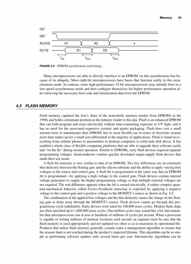
Memory 81
Many microprocessors are able to directly interface to an EPROM via this asynchronous bus be-cause of its ubiquity. Most eight-bit microprocessors have buses that function solely in this asyn-chronous mode. In contrast, some high-performance 32-bit microprocessors may initially boot in alow-speed asynchronous mode and then configure themselves for higher performance operation af-ter retrieving the necessary boot code and initialization data from the EPROM.
4.3 FLASH MEMORY
Flash memory captured the lion’s share of the nonvolatile memory market from EPROMs in the1990s and holds a dominant position as the industry leader to this day. Flash is an enhanced EPROMthat can both program and erase electrically without time-consuming exposure to UV light, and ithas no need for the associated expensive ceramic and quartz packaging. Flash does cost a smallamount more to manufacture than EPROM, but its more flexible use in terms of electronic erasuremore than makes up for a small cost differential in the majority of applications. Flash is found in ev-erything from cellular phones to automobiles to desktop computers to solid-state disk drives. It hasenabled a whole class of flexible computing platforms that are able to upgrade their software easilyand “on the fly” during normal operation. Similar to EPROMs, early flash devices required separateprogramming voltages. Semiconductor vendors quickly developed single-supply flash devices thatmade their use easier.
A flash bit structure is very similar to that of an EPROM. Two key differences are an extremelythin dielectric between the floating gate and the silicon substrate and the ability to apply varying biasvoltages to the source and control gate. A flash bit is programmed in the same way that an EPROMbit is programmed—by applying a high voltage to the control gate. Flash devices contain internalvoltage generators to supply the higher programming voltage so that multiple external voltages arenot required. The real difference appears when the bit is erased electrically. A rather complex quan-tum-mechanical behavior called
Fowler-Nordheim tunneling
is exploited by applying a negativevoltage to the control gate and a positive voltage to the MOSFET’s source as shown in Fig. 4.5.
The combination of the applied bias voltages and the thin dielectric causes the charge on the float-ing gate to drain away through the MOSFET’s source. Flash devices cannot go through this pro-gram/erase cycle indefinitely. Early devices were rated for 100,000 erase cycles. Modern flash chipsare often specified up to 1,000,000 erase cycles. One million cycles may sound like a lot, but remem-ber that microprocessors run at tens or hundreds of millions of cycles per second. When a processoris capable of writing millions of memory locations each second, an engineer must be sure that theflash memory is used appropriately and not updated too often so as to maximize its operational life.Products that utilize flash memory generally contain some a management algorithm to ensure thatthe erasure limit is not reached during the product’s expected lifetime. This algorithm can be as sim-ple as performing software updates only several times per year. Alternatively, algorithms can be
A[12:0]
D[7:0]
CE*
OE*
A1 A2 x
D1 D2
tOE tACC tOEZ
FIGURE 4.4 EPROM asynchronous read timing.
-Balch.book Page 81 Thursday, May 15, 2003 3:46 PM
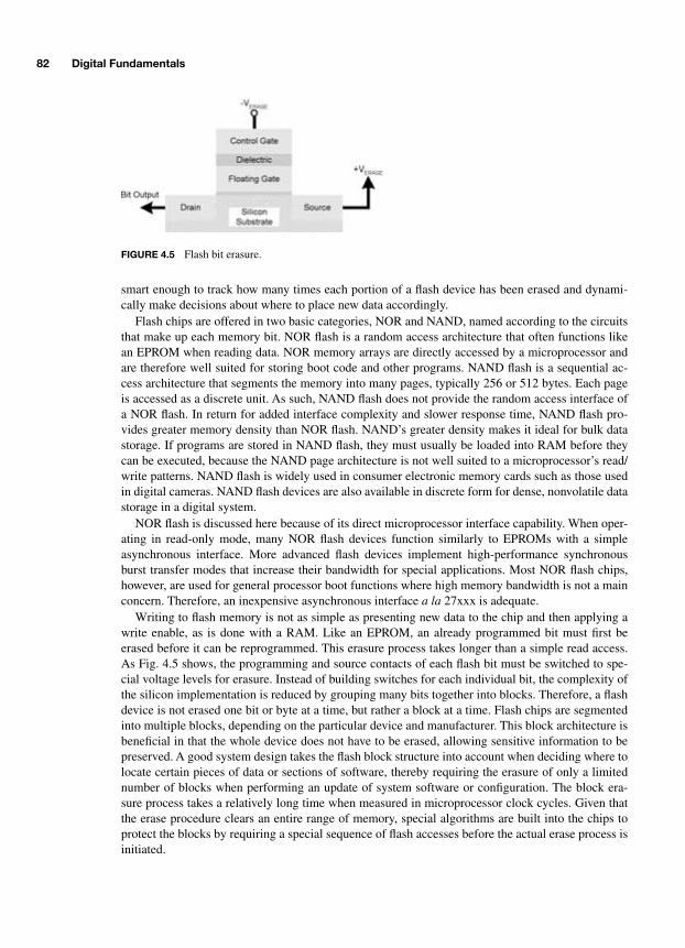
82 Digital Fundamentals
smart enough to track how many times each portion of a flash device has been erased and dynami-cally make decisions about where to place new data accordingly.
Flash chips are offered in two basic categories, NOR and NAND, named according to the circuitsthat make up each memory bit. NOR flash is a random access architecture that often functions likean EPROM when reading data. NOR memory arrays are directly accessed by a microprocessor andare therefore well suited for storing boot code and other programs. NAND flash is a sequential ac-cess architecture that segments the memory into many pages, typically 256 or 512 bytes. Each pageis accessed as a discrete unit. As such, NAND flash does not provide the random access interface ofa NOR flash. In return for added interface complexity and slower response time, NAND flash pro-vides greater memory density than NOR flash. NAND’s greater density makes it ideal for bulk datastorage. If programs are stored in NAND flash, they must usually be loaded into RAM before theycan be executed, because the NAND page architecture is not well suited to a microprocessor’s read/write patterns. NAND flash is widely used in consumer electronic memory cards such as those usedin digital cameras. NAND flash devices are also available in discrete form for dense, nonvolatile datastorage in a digital system.
NOR flash is discussed here because of its direct microprocessor interface capability. When oper-ating in read-only mode, many NOR flash devices function similarly to EPROMs with a simpleasynchronous interface. More advanced flash devices implement high-performance synchronousburst transfer modes that increase their bandwidth for special applications. Most NOR flash chips,however, are used for general processor boot functions where high memory bandwidth is not a mainconcern. Therefore, an inexpensive asynchronous interface
a la
27xxx is adequate.Writing to flash memory is not as simple as presenting new data to the chip and then applying a
write enable, as is done with a RAM. Like an EPROM, an already programmed bit must first beerased before it can be reprogrammed. This erasure process takes longer than a simple read access.As Fig. 4.5 shows, the programming and source contacts of each flash bit must be switched to spe-cial voltage levels for erasure. Instead of building switches for each individual bit, the complexity ofthe silicon implementation is reduced by grouping many bits together into blocks. Therefore, a flashdevice is not erased one bit or byte at a time, but rather a block at a time. Flash chips are segmentedinto multiple blocks, depending on the particular device and manufacturer. This block architecture isbeneficial in that the whole device does not have to be erased, allowing sensitive information to bepreserved. A good system design takes the flash block structure into account when deciding where tolocate certain pieces of data or sections of software, thereby requiring the erasure of only a limitednumber of blocks when performing an update of system software or configuration. The block era-sure process takes a relatively long time when measured in microprocessor clock cycles. Given thatthe erase procedure clears an entire range of memory, special algorithms are built into the chips toprotect the blocks by requiring a special sequence of flash accesses before the actual erase process isinitiated.
FIGURE 4.5 Flash bit erasure.
-Balch.book Page 82 Thursday, May 15, 2003 3:46 PM

Memory 83
Flash chips are not as standard as EPROMs, because different manufacturers have created theirown programming algorithms, memory organizations, and pin assignments. Many conventional par-allel data-bus devices have part numbers with “28F” or “29F” prefixes. For example, Advanced Mi-cro Devices’ flash memory family is the 29Fxxx. Intel’s family is the 28Fxxx. Aside fromprogramming differences, the size and organization of blocks within a flash device is a key func-tional difference that may make one vendor’s product better than another for a particular application.Two main attributes of flash chips are uniformity of block size and hardware protection of blocks.
Uniform-block devices divide the memory array into equally sized blocks. Boot-block devices di-vide the memory array into one or more small
boot blocks
and then divide the remainder of memoryinto equally sized blocks. Boot-block devices are popular, because the smaller boot blocks can beused to hold the rarely touched software that is used to initialize the system’s microprocessor when itfirst turns on. Boot code is often a small fraction of the system’s overall software. Due to its criticalnature, boot code is often kept simple to reduce the likelihood of errors. Therefore, boot code is sel-dom updated. In contrast, other flash ROM contents, such as application code and any applicationdata, may be updated more frequently. Using a boot-block device, a microprocessor’s boot code canbe stored away into its own block without wasting space and without requiring that it be disturbedduring a more general software update. Applications that do not store boot code in flash may notwant the complexity of dealing with nonuniform boot blocks and may therefore be better suited touniform-block devices.
Hardware protection of blocks is important when some blocks hold very sensitive informationwhose loss could cause permanent damage to the system. A common example of this is boot codestored in a boot block; if the boot code is corrupted, the CPU will fail to initialize properly the nexttime it is reset. A flash device can implement a low-level protection scheme whereby write/erase op-erations to certain blocks can be disabled with special voltage levels and data patterns presented tothe device.
Examples of real flash devices serve well to explain how this important class of nonvolatile mem-ory functions. Advanced Micro Devices (AMD) manufactures two similar flash devices: the29LV010B and the 29LV001B. Both devices are 3.3-V, 1-MB, 128k
×
8 parts that offer hardwaresector protection. The 29LV010B is a uniform-sector device, and the 29LV001B is a boot-sector de-vice. AMD uses the term
sector
instead of block. Both chips have the same basic functional bock di-agram shown in Fig. 4.6.
128k x 8Flash Array
Read, Write,Erase
ControlLogic
A[18:0] D[7:0]
CE*
OE*
WE*
DataLatch/Buffer
Programand Erase
VoltageGenerators
VCC (+3.3 V)
VSS (GND)
RESET*Present on 29LV001B only
FIGURE 4.6 AMD 29LV010B/29LV001B block diagram.
-Balch.book Page 83 Thursday, May 15, 2003 3:46 PM
84 Digital Fundamentals
Modern flash devices require only a single supply voltage and contain on-chip circuitry to createthe nonstandard programming and erasure voltages required by the memory array. Control logic de-termines which block is placed into erase or program mode at any given time as requested by the mi-croprocessor with a predefined flash control algorithm. AMD’s algorithm consists of six specialwrite transactions to the flash: two unlock cycles, a setup command, two more unlock cycles, and thespecific erase command. This sequence is detailed in Table 4.1. If interrupted, the sequence must berestarted to ensure integrity of the command.
For a whole-chip erase, the address/data in cycle 6 is 0x555/0x10. For a single-sector erase, theaddress/data in cycle 6 is the sector address/0x30. Multiple erase commands may be queued togetherto reduce the total time spent by the internal control logic erasing its sectors. While executing com-mands, the data bus is converted into a status communication mechanism. The microprocessor isable to periodically poll the device by reading from any valid address. While the erase is in progress,a value other than 0xFF will be returned. As soon as the erase has completed, the microprocessorwill read back 0xFF.
Writes to previously erased flash memory locations are accomplished with a similar technique.For each location to be programmed, a four-cycle program command sequence is performed asshown in Table 4.2. Again, the microprocessor polls for command completion by reading from thedevice. This time, however, the address polled must be the write address. When the microprocessorreads back the data that it has written, the command is known to have completed.
Other ancillary commands are supported, including device reset and identification operations.The 29LV001B includes a hardware-reset signal in addition to the soft reset command. Identification
TABLE
4.1 29LV010B/29LV001B Erase Sequence
*
*
Source:
Am29LV001B, Pub#21557, and Am29LV010B, Pub #22140,Advanced Micro Devices, 2000.
Cycle Write Address Write Data
1 0x555 0xAA
2 0x2AA 0x55
3 0x555 0x80
4 0x555 0xAA
5 0x2AA 0x55
6 Erase address Erase command
TABLE
4.2 29LV010B/29LV001B Programming Sequence
Cycle Write Address Write Data
1 0x555 0xAA
2 0x2AA 0x55
3 0x555 0xA0
4 Write address Write data
-Balch.book Page 84 Thursday, May 15, 2003 3:46 PM
Memory 85
enables the microprocessor to verify exactly which flash device it is connected to and which sectorshave been hardware protected. Identification is useful for a removable flash module that can be builtwith different parts for specific capacities. Protection status is useful so that software running on themicroprocessor can know if it is possible to program certain areas of the memory.
Hardware sector protection is accomplished during the time of system manufacture by applying ahigher than normal voltage to designated pins on the flash device using special equipment. The des-ignated pins on the 29LV010B/29LV001B are address bit 9, A9, and the output enable, OE*. Thesepins are driven to 12 V while the address of the sector to be protected is applied to other addresspins. During normal operation, there is no way for 12 V to be driven onto these signals, preventingthe protected sectors from being unprotected while in circuit. The exception to this is a feature on the29LV001B that AMD calls
temporary sector unprotect
. Previously protected sectors can be tempo-rarily unprotected by driving 12 V onto the RESET* pin with specific circuitry for this purpose. Tak-ing advantage of this feature makes it possible to modify the most sensitive areas of the flash bylocating a hardware unprotect enable signal in a logic circuit separate from the flash chip itself.
The major difference between the 29LV010B and 29LV001B is their sector organization. The29LV010B contains 8 uniform sectors of 16 kB each. The 29LV001B contains 10 sectors of nonuni-form size. Two variants of the 29LV010B are manufactured by AMD, top and bottom boot sector ar-chitectures, and their sector organization is listed in Table 4.3.
The reason for these mirrored architectures is that some microprocessors contain reset vectors to-ward the top of their address space and some toward the bottom. It is a better fit to locate the bootsectors appropriately depending on a system’s CPU. As with any complex IC, there are many detailsrelating to the operation of these flash ICs. Refer to AMD’s data sheets for more information.
4.4 EEPROM
Electrically erasable programmable ROM
, or EEPROM, is flash’s predecessor. In fact, some peoplestill refer to flash as “flash EEPROM,” because the underlying structures are very similar. EEPROM,
TABLE
4.3
29LV010B Sector Organization
Sector Number Top Boot Sector Bottom Boot Sector
0 16 kB 8 kB
1 16 kB 4 kB
2 16 kB 4 kB
3 16 kB 16 kB
4 16 kB 16 kB
5 16 kB 16 kB
6 16 kB 16 kB
7 4 kB 16 kB
8 4 kB 16 kB
9 8 kB 16 kB
-Balch.book Page 85 Thursday, May 15, 2003 3:46 PM

86 Digital Fundamentals
sometimes written as E
2
PROM, is more expensive to manufacture per bit than EPROM or flash, be-cause individual bytes may be erased randomly without affecting neighboring locations. Because ofthe complexity and associated cost of making each byte individually erasable, EEPROM is not com-monly manufactured in large densities. Instead, it has served as a niche technology for applicationsthat require small quantities of flexible reprogrammable ROM. Common uses for EEPROM are asprogram memory in small microprocessors with embedded memory and as small nonvolatile mem-ory arrays to hold system configuration information. Serial EEPROM devices can be found in eight-pin DIP or SOIC packages and provide up to several kilobytes of memory. Their serial interface,small size, and low power consumption make them very practical as a means to hold serial numbers,manufacturing information, and configuration data.
Parallel EEPROM devices are still available from manufacturers as the 28xx family. They are pinand function compatible (for reads) with the 27xxx EPROM family that they followed. Some appli-cations requiring reprogrammable nonvolatile memory may be more suited to EEPROM than flash,but flash is a compelling choice, because it is the more mainstream technology with the resultantbenefit of further cost reduction.
Serial EEPROMs, however, are quite popular due to their very small size and low power con-sumption. They can be squeezed into almost any corner of a system to provide small quantities ofnonvolatile storage. Microchip Technology is a major manufacturer of serial EEPROMs and offersthe 24xx family. Densities range from 16 bytes to several kilobytes. Given that serial interfaces usevery few pins, these EEPROMs are manufactured in packages ranging from eight-pin DIPs to five-pin SOT-23s that are smaller than a fingernail. Devices of this sort are designed to minimize systemimpact rather than for speed. Their power consumption is measured in nanoamps and microamps in-stead of milliamps, as is the case with standard flash, parallel EEPROM, and EPROM devices.
Microchip’s 24LC00 is a 16-byte serial EEPROM with a two-wire serial bus. It requires only fourpins: two for power and two for data communication. Like most modern flash devices, the 24LC00is rated for one million write cycles. When not being accessed, the 24LC00 consumes about 250 nA!When active, it consumes only 500 µA. For added flexibility, the 24LC00 can operate over a varietyof supply voltages from 2.5 to 6.0 V. Speed is not a concern here: writes take up to 4 ms to complete,which is not a problem when writing only a few bytes on rare occasions.
4.5 ASYNCHRONOUS SRAM
Static RAM
, or SRAM, is the most basic and easy to usetype of volatile memory and is found in almost every com-puter in one form or another. An SRAM device is concep-tually easy to understand, consisting of an array of latchesalong with control and decode logic to resolve the addressthat is being read or written at any given time. Each latch isa feedback circuit that traps and maintains a particularlogic state. A typical SRAM bit implementation is shown
in Fig. 4.7.An SRAM latch is created by connecting two inverters in a loop. One side of the loop remains sta-
ble at the desired logic state, and the other remains stable at the opposite state. Inverters are usedrather than noninverting buffers, because an inverter is the simplest logic element to construct. Thetwo pass transistors on either side of the latch enable both writing and reading. When writing, thetransistors turn on and force each half of the loop to whatever state is driven on the vertical bit lines.When reading, the transistors also turn on, but the bit lines are sensed rather than driven. Typical
Bit Bit
FIGURE 4.7 SRAM bit feedback latch.
-Balch.book Page 86 Thursday, May 15, 2003 3:46 PM
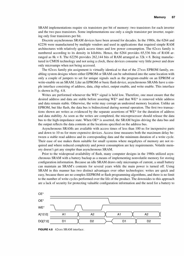
Memory 87
SRAM implementations require six transistors per bit of memory: two transistors for each inverterand the two pass transistors. Some implementations use only a single transistor per inverter, requir-ing only four transistors per bit.
Discrete asynchronous SRAM devices have been around for decades. In the 1980s, the 6264 and62256 were manufactured by multiple vendors and used in applications that required simple RAMarchitectures with relatively quick access times and low power consumption. The 62xxx family isnumbered according to its density in kilobits. Hence, the 6264 provides 65,536 bits of RAM ar-ranged as 8k
×
8. The 62256 provides 262,144 bits of RAM arranged as 32k
×
8. Being manufac-tured in CMOS technology and not using a clock, these devices consume very little power and drawonly microamps when not being accessed.
The 62xxx family pin assignment is virtually identical to that of the 27xxx EPROM family, en-abling system designs where either EPROM or SRAM can be substituted into the same location withonly a couple of jumpers to set for unique signals such as the program-enable on an EPROM orwrite-enable on an SRAM. Like an EPROM or basic flash device, asynchronous SRAMs have a sim-ple interface consisting of address, data, chip select, output enable, and write enable. This interfaceis shown in Fig. 4.8.
Writes are performed whenever the WE* signal is held low. Therefore, one must ensure that thedesired address and data are stable before asserting WE* and that WE* is removed while addressand data remain stable. Otherwise, the write may corrupt an undesired memory location. Unlike anEPROM, but like flash, the data bus is bidirectional during normal operation. The first two transac-tions shown are writes as evidenced by the separate assertions of WE* for the duration of addressand data stability. As soon as the writes are completed, the microprocessor should release the databus to the high-impedance state. When OE* is asserted, the SRAM begins driving the data bus andthe output reflects the data contents at the locations specified on the address bus.
Asynchronous SRAMs are available with access times of less than 100 ns for inexpensive partsand down to 10 ns for more expensive devices. Access time measures both the maximum delay be-tween a stable read address and its corresponding data and the minimum duration of a write cycle.Their ease of use makes them suitable for small systems where megabytes of memory are not re-quired and where reduced complexity and power consumption are key requirements. Volatile mem-ory doesn’t get any simpler than asynchronous SRAM.
Prior to the widespread availability of flash, many computer designs in the 1980s utilized asyn-chronous SRAM with a battery backup as a means of implementing nonvolatile memory for storingconfiguration information. Because an idle SRAM draws only microamps of current, a small batterycan maintain an SRAM’s contents for several years while the main power is turned off. UsingSRAM in this manner has two distinct advantages over other technologies: writes are quick andeasy, because there are no complex EEPROM or flash programming algorithms, and there is no limitto the number of write cycles performed over the life of the product. The downsides to this approachare a lack of security for protecting valuable configuration information and the need for a battery to
A[12:0]
DQ[7:0]
CE*
OE*
A1 A2
D1 D2
WE*
A1 A2
D1 D2
FIGURE 4.8 62xxx SRAM interface.
-Balch.book Page 87 Thursday, May 15, 2003 3:46 PM
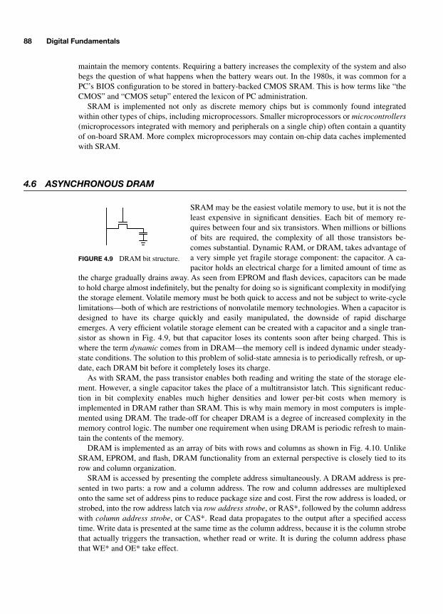
88 Digital Fundamentals
maintain the memory contents. Requiring a battery increases the complexity of the system and alsobegs the question of what happens when the battery wears out. In the 1980s, it was common for aPC’s BIOS configuration to be stored in battery-backed CMOS SRAM. This is how terms like “theCMOS” and “CMOS setup” entered the lexicon of PC administration.
SRAM is implemented not only as discrete memory chips but is commonly found integratedwithin other types of chips, including microprocessors. Smaller microprocessors or
microcontrollers
(microprocessors integrated with memory and peripherals on a single chip) often contain a quantityof on-board SRAM. More complex microprocessors may contain on-chip data caches implementedwith SRAM.
4.6 ASYNCHRONOUS DRAM
SRAM may be the easiest volatile memory to use, but it is not theleast expensive in significant densities. Each bit of memory re-quires between four and six transistors. When millions or billionsof bits are required, the complexity of all those transistors be-comes substantial. Dynamic RAM, or DRAM, takes advantage ofa very simple yet fragile storage component: the capacitor. A ca-pacitor holds an electrical charge for a limited amount of time as
the charge gradually drains away. As seen from EPROM and flash devices, capacitors can be madeto hold charge almost indefinitely, but the penalty for doing so is significant complexity in modifyingthe storage element. Volatile memory must be both quick to access and not be subject to write-cyclelimitations—both of which are restrictions of nonvolatile memory technologies. When a capacitor isdesigned to have its charge quickly and easily manipulated, the downside of rapid dischargeemerges. A very efficient volatile storage element can be created with a capacitor and a single tran-sistor as shown in Fig. 4.9, but that capacitor loses its contents soon after being charged. This iswhere the term
dynamic
comes from in DRAM—the memory cell is indeed dynamic under steady-state conditions. The solution to this problem of solid-state amnesia is to periodically refresh, or up-date, each DRAM bit before it completely loses its charge.
As with SRAM, the pass transistor enables both reading and writing the state of the storage ele-ment. However, a single capacitor takes the place of a multitransistor latch. This significant reduc-tion in bit complexity enables much higher densities and lower per-bit costs when memory isimplemented in DRAM rather than SRAM. This is why main memory in most computers is imple-mented using DRAM. The trade-off for cheaper DRAM is a degree of increased complexity in thememory control logic. The number one requirement when using DRAM is periodic refresh to main-tain the contents of the memory.
DRAM is implemented as an array of bits with rows and columns as shown in Fig. 4.10. UnlikeSRAM, EPROM, and flash, DRAM functionality from an external perspective is closely tied to itsrow and column organization.
SRAM is accessed by presenting the complete address simultaneously. A DRAM address is pre-sented in two parts: a row and a column address. The row and column addresses are multiplexedonto the same set of address pins to reduce package size and cost. First the row address is loaded, orstrobed, into the row address latch via
row address strobe
, or RAS*, followed by the column addresswith
column address strobe
, or CAS*. Read data propagates to the output after a specified accesstime. Write data is presented at the same time as the column address, because it is the column strobethat actually triggers the transaction, whether read or write. It is during the column address phasethat WE* and OE* take effect.
FIGURE 4.9 DRAM bit structure.
-Balch.book Page 88 Thursday, May 15, 2003 3:46 PM

Memory 89
Sense amplifiers on the chip are necessary to detect the minute charges that are held in theDRAM’s capacitors. These amplifiers are also used to assist in refresh operations. It is the memorycontroller’s responsibility to maintain a refresh timer and initiate refresh operations with sufficientfrequency to guarantee data integrity. Rather than refreshing each bit separately, an entire row is re-freshed at the same time. An internal refresh counter increments after each refresh so that all rows,and therefore all bits, will be cycled through in order. When a refresh begins, the refresh counterenables a particular memory row. The contents of the row are detected by the sense amplifiers andthen driven back into the bit array to recharge all the capacitors in that row. Modern DRAMs typi-cally require a complete refresh every 64 ms. A 64-Mb DRAM organized as 8,388,608 words
×
8bits (8 MB) with an internal array size of 4,096
×
2,048 bytes would require 4,096 refresh cyclesevery 64 ms. Refresh cycles need not be evenly spaced in time but are often spread uniformly forsimplicity.
The complexity of performing refresh is well worth the trouble because of the substantial cost anddensity improvements over SRAM. One downside of DRAM that can only be partially compensatedfor is its slower access time. A combination of its multiplexed row and column addressing schemeplus its large memory arrays with complex sense and decode logic make DRAM significantly slowerthan SRAM. Mainstream computing systems deal with this speed problem by implementing SRAM-based cache mechanisms whereby small chunks of memory are prefetched into fast SRAM so thatthe microprocessor does not have to wait as long for new data that it requests.
Asynchronous DRAM was the prevailing DRAM technology until the late 1990s, when synchro-nous DRAM, or SDRAM, emerged as the dominant solution to main memory. At its heart, SDRAMworks very much like DRAM but with a synchronous bus interface that enables faster memory trans-actions. It is useful to explore how older asynchronous DRAM works so as to understand SDRAM.SDRAM will be covered in detail later in the book.
RAS* and CAS* are the two main DRAM control signals. They not only tell the DRAM chipwhich address is currently being asserted, they also initiate refresh cycles and accelerate sequentialtransactions to increase performance. A basic DRAM read works as shown in Fig. 4.11. CE* andOE* are both assumed to be held active (low) throughout the transaction.
A transaction begins by asserting RAS* to load the row address. The strobes are falling-edge sen-sitive, meaning that the address is loaded on the falling edge of the strobe, sometime after which theaddress may change. Asynchronous DRAMs are known for their myriad detailed timing require-ments. Every signal’s timing relative to itself and other signals is specified in great detail, and theseparameters must be obeyed for reliable operation. RAS* is kept low for the duration of the transac-tion. Assertion of CAS* loads the column address into the DRAM as well as the read or write status
N x MDRAMArray
SenseAmplifiers
Address
Data
Row AddressLatch
Control
RefreshCounter
ColumnAddress Latch
Control LogicRAS*, CAS*,WE*, OE*, CE*
FIGURE 4.10 DRAM architecture.
-Balch.book Page 89 Thursday, May 15, 2003 3:46 PM
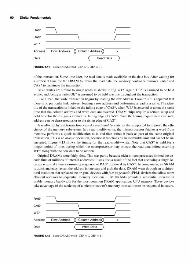
90 Digital Fundamentals
of the transaction. Some time later, the read data is made available on the data bus. After waiting fora sufficient time for the DRAM to return the read data, the memory controller removes RAS* andCAS* to terminate the transaction.
Basic writes are similar to single reads as shown in Fig. 4.12. Again, CE* is assumed to be heldactive, and, being a write, OE* is assumed to be held inactive throughout the transaction.
Like a read, the write transaction begins by loading the row address. From this it is apparent thatthere is no particular link between loading a row address and performing a read or a write. The iden-tity of the transaction is linked to the falling edge of CAS*, when WE* is asserted at about the sametime that the column address and write data are asserted. DRAM chips require a certain setup andhold time for these signals around the falling edge of CAS*. Once the timing requirements are met,address can be deasserted prior to the rising edge of CAS*.
A read/write hybrid transaction, called a
read-modify-write
, is also supported to improve the effi-ciency of the memory subsystem. In a read-modify-write, the microprocessor fetches a word frommemory, performs a quick modification to it, and then writes it back as part of the same originaltransaction. This is an
atomic
operation, because it functions as an indivisible unit and cannot be in-terrupted. Figure 4.13 shows the timing for the read-modify-write. Note that CAS* is held for alonger period of time, during which the microprocessor may process the read-data before assertingWE* along with the new data to be written.
Original DRAMs were fairly slow. This was partly because older silicon processes limited the de-code time of millions of internal addresses. It was also a result of the fact that accessing a single lo-cation required a time-consuming sequence of RAS* followed by CAS*. In comparison, an SRAMis quick and easy: assert the address in one step and grab the data. DRAM went through an architec-tural evolution that replaced the original devices with
fast-page mode
(FPM) devices that allow moreefficient accesses to sequential memory locations. FPM DRAMs provide a substantial increase inusable memory bandwidth for the most common DRAM application: CPU memory. These devicestake advantage of the tendency of a microprocessor’s memory transactions to be sequential in nature.
Address
Data
CAS*
Row Address Column Address
WE*
Read Data
RAS*
x
FIGURE 4.11 Basic DRAM read (CE* = 0, OE* = 0).
Address
Data
CAS*
Row Address Column Address
WE*
Write Data
RAS*
x
FIGURE 4.12 Basic DRAM write (CE* = 0, OE* = 1).
-Balch.book Page 90 Thursday, May 15, 2003 3:46 PM

Memory 91
Software does occasionally branch back and forth in its memory space. Yet, on the whole, softwaremoves through portions of memory in a linear fashion. FPM devices enable a DRAM controller toload a row-address in the normal manner using RAS* and then perform multiple CAS* transactionsusing the same row-address. Therefore, DRAMs end their transaction cycles with the rising edge ofRAS*, because they cannot be sure if more reads or writes are coming until RAS* rises, indicatingthat the current row-address can be released.
FPM technology, in turn, gave way to
extended-data out
(EDO) devices that extend the time readdata is held valid. Unlike its predecessors, an EDO DRAM does not disable the read data whenCAS* rises. Instead, it waits until either the transaction is complete (RAS* rises), OE* is deasserted,or until CAS* begins a new page-mode access. While FPM and EDO DRAMs are distinct types ofdevices, EDO combines the page-mode features of FPM and consequently became more attractive touse. The following timing discussion uses EDO functionality as the example.
Page-mode transactions hold RAS* active and cycle CAS* multiple times to perform reads andwrites as shown in Figs. 4.14 and 4.15. Each successive CAS* falling edge loads a new column ad-dress and causes either a read or write to be performed. In the read case, EDO’s benefit can be properlyobserved. Rather than read data being removed when CAS* rises, it remains asserted until just after thenext falling edge of CAS* or the rising edge of RAS* that terminates the page-mode transaction.
Address
Data
CAS*
Row Address Column Address
WE*
RAS*
x
OE*
Write DataRead Data
FIGURE 4.13 Read-modify-write transaction.
Address
Data
CAS*
Row Address Col Addr 1
RAS*
Read Data 1
Col Addr 2 Col Addr 3
Read Data 2 Read Data 3
FIGURE 4.14 Page-mode reads.
Address
Data
CAS*
Row Address Col Addr 1
RAS*
Col Addr 2 Col Addr 3
Write Data 2Write Data 1 Write Data 3
FIGURE 4.15 Page-mode writes.
-Balch.book Page 91 Thursday, May 15, 2003 3:46 PM
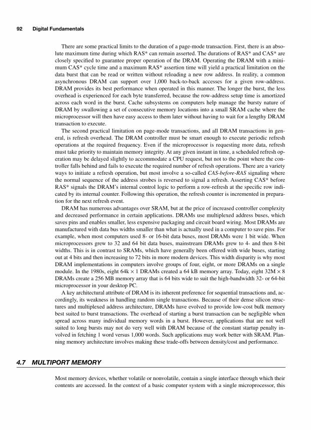
92 Digital Fundamentals
There are some practical limits to the duration of a page-mode transaction. First, there is an abso-lute maximum time during which RAS* can remain asserted. The durations of RAS* and CAS* areclosely specified to guarantee proper operation of the DRAM. Operating the DRAM with a mini-mum CAS* cycle time and a maximum RAS* assertion time will yield a practical limitation on thedata burst that can be read or written without reloading a new row address. In reality, a commonasynchronous DRAM can support over 1,000 back-to-back accesses for a given row-address.DRAM provides its best performance when operated in this manner. The longer the burst, the lessoverhead is experienced for each byte transferred, because the row-address setup time is amortizedacross each word in the burst. Cache subsystems on computers help manage the bursty nature ofDRAM by swallowing a set of consecutive memory locations into a small SRAM cache where themicroprocessor will then have easy access to them later without having to wait for a lengthy DRAMtransaction to execute.
The second practical limitation on page-mode transactions, and all DRAM transactions in gen-eral, is refresh overhead. The DRAM controller must be smart enough to execute periodic refreshoperations at the required frequency. Even if the microprocessor is requesting more data, refreshmust take priority to maintain memory integrity. At any given instant in time, a scheduled refresh op-eration may be delayed slightly to accommodate a CPU request, but not to the point where the con-troller falls behind and fails to execute the required number of refresh operations. There are a varietyways to initiate a refresh operation, but most involve a so-called
CAS-before-RAS
signaling wherethe normal sequence of the address strobes is reversed to signal a refresh. Asserting CAS* beforeRAS* signals the DRAM’s internal control logic to perform a row-refresh at the specific row indi-cated by its internal counter. Following this operation, the refresh counter is incremented in prepara-tion for the next refresh event.
DRAM has numerous advantages over SRAM, but at the price of increased controller complexityand decreased performance in certain applications. DRAMs use multiplexed address buses, whichsaves pins and enables smaller, less expensive packaging and circuit board wiring. Most DRAMs aremanufactured with data bus widths smaller than what is actually used in a computer to save pins. Forexample, when most computers used 8- or 16-bit data buses, most DRAMs were 1 bit wide. Whenmicroprocessors grew to 32 and 64 bit data buses, mainstream DRAMs grew to 4- and then 8-bitwidths. This is in contrast to SRAMs, which have generally been offered with wide buses, startingout at 4 bits and then increasing to 72 bits in more modern devices. This width disparity is why mostDRAM implementations in computers involve groups of four, eight, or more DRAMs on a singlemodule. In the 1980s, eight 64k
×
1 DRAMs created a 64 kB memory array. Today, eight 32M
×
8DRAMs create a 256 MB memory array that is 64 bits wide to suit the high-bandwidth 32- or 64-bitmicroprocessor in your desktop PC.
A key architectural attribute of DRAM is its inherent preference for sequential transactions and, ac-cordingly, its weakness in handling random single transactions. Because of their dense silicon struc-tures and multiplexed address architecture, DRAMs have evolved to provide low-cost bulk memorybest suited to burst transactions. The overhead of starting a burst transaction can be negligible whenspread across many individual memory words in a burst. However, applications that are not wellsuited to long bursts may not do very well with DRAM because of the constant startup penalty in-volved in fetching 1 word versus 1,000 words. Such applications may work better with SRAM. Plan-ning memory architecture involves making these trade-offs between density/cost and performance.
4.7 MULTIPORT MEMORY
Most memory devices, whether volatile or nonvolatile, contain a single interface through which theircontents are accessed. In the context of a basic computer system with a single microprocessor, this
-Balch.book Page 92 Thursday, May 15, 2003 3:46 PM

Memory 93
single-port
architecture is well suited. There are some architectures in which multiple microproces-sors or logic blocks require access to the same shared pool of memory. A shared pool of memory canbe constructed in a couple of ways. First, conventional DRAM or SRAM can be combined with ex-ternal logic that takes requests from separate entities (e.g., microprocessors) and arbitrates access toone requestor at a time. When the shared memory pool is large, and when simultaneous access bymultiple requesters is not required, arbitration can be an efficient mechanism. However, the com-plexity of arbitration logic may be excessive for small shared-memory pools, and arbitration doesnot enable simultaneous access. A means of sharing memory without arbitration logic and with si-multaneous access capability is to construct a true multiport memory element.
A multiport memory provides simultaneous access to multiple external entities. Each port maybe read/write capable, read-only, or write-only depending on the implementation and application.Multiport memories are generally kept relatively small, because their complexity, and hence theircost, increases significantly as additional ports are added, each with its own decode and controllogic. Most multiport memories are
dual-port
elements as shown in Fig. 4.16.A true dual-port memory places no restrictions on either port’s transactions at any given time. It is
the responsibility of the engineer to ensure that one requester does not conflict with the other. Con-flicts arise when one requester writes a memory location while the other is either reading or writingthat same location. If a simultaneous read/write occurs, what data does the reader see? Is it the databefore or after the write? Likewise, if two writes proceed at the same time, which one wins? Whilethese riddles could be worked out for specific applications with custom logic, it is safer not to worryabout such corner cases. Instead, the system design should avoid such conflicts unless there is astrong reason to the contrary.
One common application of a dual-port memory is sharing information between two micropro-cessors as shown in Fig. 4.17. A dual-port memory sits between the microprocessors and can be par-titioned into a separate message bin, or memory area, for each side. Bin A contains messages writtenby CPU A and read by CPU B. Bin B contains messages written by CPU B and read by CPU A.
Notification of a waiting message is accomplished via a CPU interrupt, thereby releasing theCPUs from having to constantly poll the memory as they wait for messages to arrive. The entire pro-cess might work as follows:
1. CPU A writes a message for CPU B into Bin A.
2. CPU A asserts an interrupt to CPU B indicating the a message is waiting in Bin A.
3. CPU B reads the message in Bin A.
4. CPU B acknowledges the interrupt from CPU A.
5. CPU A releases the interrupt to CPU B.
An implementation like this prevents dual-port memory conflicts because one CPU will not read amessage before it has been fully written by the other CPU and neither CPU writes to both bins.
Dual-PortMemory
Array
Port AControlLogic
Port BControlLogic
FIGURE 4.16 Dual-port memory.
-Balch.book Page 93 Thursday, May 15, 2003 3:46 PM

94 Digital Fundamentals
4.8 THE FIFO
The memory devices discussed thus far are essentially linear arrays of bits surrounded by a minimalquantity of interface logic to move bits between the port(s) and the array.
First-in-first-out
(FIFO)memories are special-purpose devices that implement a basic queue structure that has broad applica-tion in computer and communications architecture. Unlike other memory devices, a typical FIFOhas two unidirectional ports without address inputs: one for writing and another for reading. As thename implies, the first data written is the first read, and the last data written is the last read. A FIFOis not a random access memory but a sequential access memory. Therefore, unlike a conventionalmemory, once a data element has been read once, it cannot be read again, because the next read willreturn the next data element written to the FIFO. By their nature, FIFOs are subject to
overflow
and
underflow
conditions. Their finite size, often referred to as
depth
, means that they can fill up if readsdo not occur to empty data that has already been written. An overflow occurs when an attempt ismade to write new data to a full FIFO. Similarly, an empty FIFO has no data to provide on a read re-quest, which results in an underflow.
A FIFO is created by surrounding a dual-port memory array—generally SRAM, but DRAMcould be made to work as well for certain applications—with a write pointer, a read pointer, and con-trol logic as shown in Fig. 4.18.
Dual-Port Memory
CPU A
Message Bin A
Message Bin B
CPU B
InterruptLogic
InterruptLogic
"Message Ready"
FIGURE 4.17 Dual microprocessor message passing architecture.
Dual-Port Memory Array
WritePointer
ReadPointer
ComparisonLogic
WriteControl
Interface
Full
ReadControl
Interface
Empty
Write Data
Write Enable
Full
Read Data
Read Enable
Empty
write data read data
write address read address
FIGURE 4.18 Basic FIFO architecture.
-Balch.book Page 94 Thursday, May 15, 2003 3:46 PM
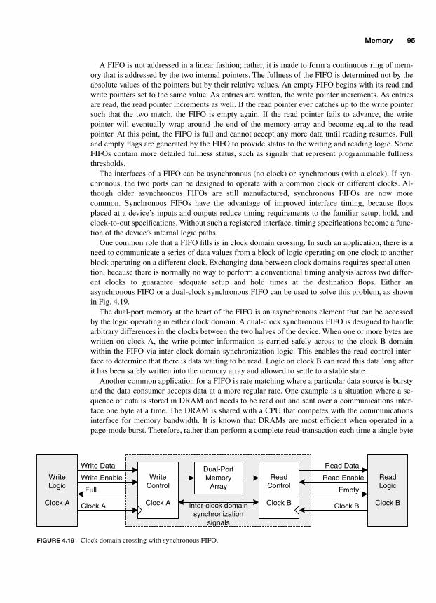
Memory 95
A FIFO is not addressed in a linear fashion; rather, it is made to form a continuous ring of mem-ory that is addressed by the two internal pointers. The fullness of the FIFO is determined not by theabsolute values of the pointers but by their relative values. An empty FIFO begins with its read andwrite pointers set to the same value. As entries are written, the write pointer increments. As entriesare read, the read pointer increments as well. If the read pointer ever catches up to the write pointersuch that the two match, the FIFO is empty again. If the read pointer fails to advance, the writepointer will eventually wrap around the end of the memory array and become equal to the readpointer. At this point, the FIFO is full and cannot accept any more data until reading resumes. Fulland empty flags are generated by the FIFO to provide status to the writing and reading logic. SomeFIFOs contain more detailed fullness status, such as signals that represent programmable fullnessthresholds.
The interfaces of a FIFO can be asynchronous (no clock) or synchronous (with a clock). If syn-chronous, the two ports can be designed to operate with a common clock or different clocks. Al-though older asynchronous FIFOs are still manufactured, synchronous FIFOs are now morecommon. Synchronous FIFOs have the advantage of improved interface timing, because flopsplaced at a device’s inputs and outputs reduce timing requirements to the familiar setup, hold, andclock-to-out specifications. Without such a registered interface, timing specifications become a func-tion of the device’s internal logic paths.
One common role that a FIFO fills is in clock domain crossing. In such an application, there is aneed to communicate a series of data values from a block of logic operating on one clock to anotherblock operating on a different clock. Exchanging data between clock domains requires special atten-tion, because there is normally no way to perform a conventional timing analysis across two differ-ent clocks to guarantee adequate setup and hold times at the destination flops. Either anasynchronous FIFO or a dual-clock synchronous FIFO can be used to solve this problem, as shownin Fig. 4.19.
The dual-port memory at the heart of the FIFO is an asynchronous element that can be accessedby the logic operating in either clock domain. A dual-clock synchronous FIFO is designed to handlearbitrary differences in the clocks between the two halves of the device. When one or more bytes arewritten on clock A, the write-pointer information is carried safely across to the clock B domainwithin the FIFO via inter-clock domain synchronization logic. This enables the read-control inter-face to determine that there is data waiting to be read. Logic on clock B can read this data long afterit has been safely written into the memory array and allowed to settle to a stable state.
Another common application for a FIFO is rate matching where a particular data source is burstyand the data consumer accepts data at a more regular rate. One example is a situation where a se-quence of data is stored in DRAM and needs to be read out and sent over a communications inter-face one byte at a time. The DRAM is shared with a CPU that competes with the communicationsinterface for memory bandwidth. It is known that DRAMs are most efficient when operated in apage-mode burst. Therefore, rather than perform a complete read-transaction each time a single byte
Dual-PortMemory
ArrayWrite
Control
Clock A
Write Data
Write Enable
Full
Read Data
Read Enable
Empty
ReadControl
Clock B
WriteLogic
Clock A
ReadLogic
Clock Binter-clock domainsynchronization
signals
Clock BClock A
FIGURE 4.19 Clock domain crossing with synchronous FIFO.
-Balch.book Page 95 Thursday, May 15, 2003 3:46 PM
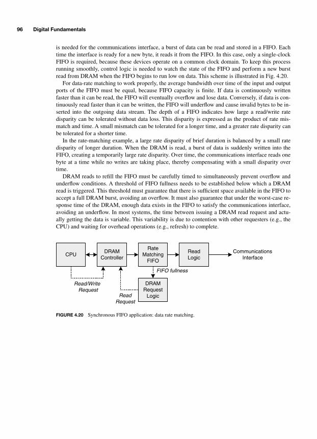
96 Digital Fundamentals
is needed for the communications interface, a burst of data can be read and stored in a FIFO. Eachtime the interface is ready for a new byte, it reads it from the FIFO. In this case, only a single-clockFIFO is required, because these devices operate on a common clock domain. To keep this processrunning smoothly, control logic is needed to watch the state of the FIFO and perform a new burstread from DRAM when the FIFO begins to run low on data. This scheme is illustrated in Fig. 4.20.
For data-rate matching to work properly, the average bandwidth over time of the input and outputports of the FIFO must be equal, because FIFO capacity is finite. If data is continuously writtenfaster than it can be read, the FIFO will eventually overflow and lose data. Conversely, if data is con-tinuously read faster than it can be written, the FIFO will underflow and cause invalid bytes to be in-serted into the outgoing data stream. The depth of a FIFO indicates how large a read/write ratedisparity can be tolerated without data loss. This disparity is expressed as the product of rate mis-match and time. A small mismatch can be tolerated for a longer time, and a greater rate disparity canbe tolerated for a shorter time.
In the rate-matching example, a large rate disparity of brief duration is balanced by a small ratedisparity of longer duration. When the DRAM is read, a burst of data is suddenly written into theFIFO, creating a temporarily large rate disparity. Over time, the communications interface reads onebyte at a time while no writes are taking place, thereby compensating with a small disparity overtime.
DRAM reads to refill the FIFO must be carefully timed to simultaneously prevent overflow andunderflow conditions. A threshold of FIFO fullness needs to be established below which a DRAMread is triggered. This threshold must guarantee that there is sufficient space available in the FIFO toaccept a full DRAM burst, avoiding an overflow. It must also guarantee that under the worst-case re-sponse time of the DRAM, enough data exists in the FIFO to satisfy the communications interface,avoiding an underflow. In most systems, the time between issuing a DRAM read request and actu-ally getting the data is variable. This variability is due to contention with other requesters (e.g., theCPU) and waiting for overhead operations (e.g., refresh) to complete.
RateMatching
FIFO
DRAMController
DRAMRequest
Logic
CommunicationsInterface
FIFO fullness
ReadRequest
CPU
Read/WriteRequest
ReadLogic
FIGURE 4.20 Synchronous FIFO application: data rate matching.
-Balch.book Page 96 Thursday, May 15, 2003 3:46 PM

97
CHAPTER 5
Serial Communications
Serial communication interfaces are commonly used to exchange data with other computers. Serialinterfaces are ubiquitous, because they are economical to implement over long distances as a resultof their requirement of relatively few wires. Many types of serial interfaces have been developed,with speeds ranging to billions of bits per second. Regardless of the bit rate, serial communicationinterfaces share many common traits. This chapter introduces the fundamentals of serial communi-cation in the context of popular data links such as RS-232 and RS-485 in which bandwidths andcomponents lend themselves to basic circuit fabrication techniques.
The chapter first deals with the basic parallel-to-serial-to-parallel conversion process that is at theheart of all serial communication. Wide buses must be serialized at the transmitter and reconstructedat the receiver. Techniques for accomplishing this vary with the specific type of data link, but basicconcepts of framing and error detection are universal.
Two widely deployed point-to-point serial communication standards, RS-232 and RS-422, arepresented, along with the standard ASCII character set, to see how theory meets practice. Standardsare important to communications in general because of the need to connect disparate equipment.ASCII is one of the most fundamental data representation formats with global recognition. RS-232has traditionally been found in many digital systems, because it is a reliable standard. UnderstandingRS-232, its relative RS-422, and ASCII enables an engineer to design a communication interfacethat can work with an almost infinite range of complementary equipment ranging from computers tomodems to off-the-shelf peripherals.
Systems may require more advanced communication schemes to enable data exchange betweenmany nodes. Networks enable such communication and can range in complexity according to an ap-plication’s requirements. Networking adds a new set of fundamental concepts on top of basic serialcommunication. Topics including network topologies and packet formats are presented to explainhow networks function at a basic hardware and software level. Once networking fundamentals havebeen discussed, the RS-485 standard is introduced to show how a simple and fully functional net-work can be constructed. A complete network design example using RS-485 is offered with explana-tions of why various design points are included and how they contribute to the network’s overalloperation.
The chapter closes with a presentation of small-scale networking employed within a digital sys-tem to economically connect peripherals to a microprocessor. Interchip networks are of such narrowscope that they are usually not referred to as networks, but they can possess many fundamental prop-erties of a larger network. Peripherals with low microprocessor bandwidth requirements can be con-nected using a simple serial interface consisting of just a few wires, as compared to the fullcomplexity of a parallel bus.
-Balch.book Page 97 Thursday, May 15, 2003 3:46 PM
Copyright 2003 by The McGraw-Hill Companies, Inc. Click Here for Terms of Use.

98 Digital Fundamentals
5.1 SERIAL VS. PARALLEL COMMUNICATION
Most logical operations and data processing occur in parallel on multiple bits simultaneously. Mi-croprocessors, for example, have wide data buses to increase throughput. With wide buses comes arequirement for more wires to connect the logical elements in a system. The interconnection penaltyincreases as distances increase. Within a chip, the penalty is small, and wide buses are common. Im-plementing wide buses on a circuit board is also common because of the relatively short distancesinvolved.
The economics and technical context of interconnect changes as soon as the distances grow fromcentimeters to meters to kilometers. Communication is primarily concerned with transporting datafrom one location to another rather than processing that information as it is carried on a wire. Withdistance comes the expensive problem of stringing a continuous wire between two locations.Whether the wire is threaded through a conduit between floors in an office, buried under the streetbetween buildings, or virtually constructed via radio transmission to a satellite, the cost and com-plexity of connecting multiple wires is many orders of magnitude greater than on a circuit board. Se-rial communication is well suited to long distances, because fewer wires are used as compared to aparallel bus. A serial data link implies a single-wire medium, but there can be multiwire serial linksas well.
Figure 5.1 illustrates several logical components in a serial data link. At either end are the sourcesand consumers of the data that operate using a parallel bus. A
transceiver
converts between a parallelbus and a serial stream and handles any link-level timing necessary to properly send and receivedata. A
transducer
, or
modulator
in wireless links, converts between the medium’s electromagneticsignaling characteristics and the transceiver’s logic-level signals. Finally, a conductive path joins thetwo transducers. This path can be copper wire, glass fiber optic cable, or free space. These logicalcomponents may be integrated in arbitrary physical configurations in different implementations, sonot all serial links will consist of three specific discrete pieces. Simple links may have fewer pieces,and complex links may have more.
The total cost of a data link is the sum of the cost of the transceiver/transducer subsystems at eachend and the cost of the physical medium itself. A serial port on a desktop computer is inexpensivebecause of its relatively simple electronic circuits and because the medium over which it communi-cates, a short copper wire, is fairly cheap. In contrast, a satellite link is very expensive as a result ofthe greater complexity of the ground-based transmission equipment, the high cost of the satellite it-self, and the licensing costs of using the public airwaves.
If only one bit is transferred per clock cycle in a serial link, it follows that either the serial bitclock has to be substantially faster than the parallel bus, or the link’s
bandwidth
will be significantly
Data Processor
Transceiver
Transducer
Data Processor
Transceiver
Transducer
parallel data
serial data
communications medium
FIGURE 5.1 Components of a serial data link.
-Balch.book Page 98 Thursday, May 15, 2003 3:46 PM

Serial Communications 99
below that of the parallel bus.
Bandwidth
in a communication context refers to the capacity of thecommunications channel, often expressed either in bits-per-second (bps) or bytes-per-second (Bps).Serial links are available in a broad spectrum of bandwidths, from thousands of bits per second(kbps) to billions of bits per second (Gbps) and are stretching toward trillions of bits per second(Tbps)!
Most implementations in the kbps range involve applications where relatively small quantities ofdata are exchanged, so the cost of deploying an advanced data link is not justified. These serial linksare able to run at low frequencies (several hundred kilohertz and below) and therefore do not requirecomplex circuitry. Of course, some low-bandwidth data links can be very expensive if the mediumover which they operate presents extreme technical difficulties, such as communicating across inter-planetary distances. Implementations in the Gbps range serve applications such as high-end com-puter networks where huge volumes of data are carried. Such links are run at gigahertz frequenciesand are relatively costly due to this high level of performance. Gigahertz serial transfer rates do nottranslate into similar logic clock frequencies. When a transceiver converts a serial data stream into aparallel bus, it contains the very high frequency complexity within itself. A 1-Gbps link requiresonly a 31.25 MHz clock when using a 32-bit data path.
5.2 THE UART
The
universal asynchronous receiver/transmitter
(UART) is a basic transceiver element that serial-izes a parallel bus when transmitting and deserializes the incoming stream when receiving. In addi-tion to bus-width conversion, the UART also handles overhead and synchronization functionsrequired to transport data. Data bits cannot simply be serialized onto a wire without some additionalinformation to delineate the start and end of each unit of data. This delineation is called
framing
. Thereceiver must be able to recognize the start of a byte so that it can synchronize its shift registers andreceive logic to properly capture the data. Basic framing is accomplished with a
start bit
that is as-signed a logic state opposite to that of the transmission medium’s idle state, often logic 1 for histori-cal reasons. When no data is being sent, the transmission medium, typically a wire, may be driven tologic 1. A logic 0 start bit signals the receiver that data is on the way. The receiving UART must beconfigured to handle the same number of data bits sent by the transmitter. Either seven or eight databits are supported by most UARTs. After seven or eight data bits have been captured following thestart bit, the UART knows that the data unit has completed and it can resume waiting for a new startbit. One or more
stop bits
follow to provide a minimum delay between successive data units so thatthe receiver can complete processing of the current datum before receiving the next one.
Many UARTs also support some form of error detection in the form of a
parity bit
. The parity bitis the XOR of the data bits and is sent along with data so that it can be recalculated and verified atthe receiver. Error detection is considered more important on a long-distance data link, as comparedto on a circuit board, because errors are more prone over longer distances. A parity bit is added toeach data unit, most often each byte, that tells the receiver if an odd or even number of 1s are in thedata word. The receiver and transmitter must be configured to agree on whether even or odd parity isbeing implemented. Even parity is calculated by XORing all data bits, and odd parity is calculatedby inverting even parity. The result is that, for even parity, the parity bit will be set if there are an oddnumber of 1s in the byte. Conversely, the parity bit will be cleared if there are an odd number of 1spresent. Odd parity is just the opposite, as shown in Fig. 5.2.
Handshaking
is another common feature of UARTs. Handshaking, also called
flow control
, is thegeneral process whereby two ends of a data link confirm that each is ready to exchange data beforethe actual exchange occurs. The process can use hardware or software signaling. Hardware hand-
-Balch.book Page 99 Thursday, May 15, 2003 3:46 PM

100 Digital Fundamentals
shaking involves a receiver driving a ready signal to the transmitter. The transmitter sends data onlywhen the receiver signals that it is ready. UARTs may support hardware handshaking. Any softwarehandshaking is the responsibility of the UART control program.
Software handshaking works by transmitting special binary codes that either pause or resume theopposite end as it sends data.
XON
/
XOFF
handshaking is a common means of implementing soft-ware flow control. When one end of the link is ready to accept data, it transmits a standard charactercalled XON (0x11) to the opposite device. When the receiver has filled a buffer and is unable to ac-cept more data, an XOFF character (0x13) is transmitted. It is by good behavior that most flow con-trol schemes work: the device that receives an XOFF must respect the signal and pause itstransmission until an XON is received. It is not uncommon to see an XON/XOFF setting in certainserial terminal configurations.
A generic UART is shown in Fig. 5.3. The UART is divided into three basic sections: CPU inter-face, transmitter, and receiver. The CPU interface contains various registers to configure parity, bit rate,handshaking, and interrupts. UARTs usually provide three parity options: none, even, and odd. Bit rateis selectable well by programming an internal counter to arbitrarily divide an external reference clock.The range of usable bit clocks may be from several hundred bits per second to over 100 kbps.
Interrupts are used to inform the CPU when a new byte has been received and when a new byte isready to be transmitted. This saves the CPU from having to constantly poll the UART’s status regis-ters for this information. However, UARTs provide status bits to aid in interrupt status reporting, soa simple serial driver program could operate by polling rather than implementing an interrupt serviceroutine. Aside from general control and status registers, the CPU interface provides access to trans-mit and receive buffers so that data can be queued for transmission and retrieved upon arrival. De-pending on the UART, these buffers may be only one byte each, or they may be several bytes
0xA0 = 10100000 0
Even ParityData
1
Odd Parity
FIGURE 5.2 Odd and even parity.
CPUInterface
Logic
ControlRegisters
StatusRegisters
ReceiveBuffer
TransmitBuffer
Data
Address, Control
Interrupt
Tx ShiftLogic
ParityGenerator
Rx ShiftLogic
ParityChecker
ClockSync
Bit ClockDivider
Reference Clock
Serial Out
Serial In
Handshaking Out
Handshaking In
FIGURE 5.3 Generic UART block diagram.
-Balch.book Page 100 Thursday, May 15, 2003 3:46 PM

Serial Communications 101
implemented as a small FIFO. Typically, these serial ports run slow enough to not require deep buff-ers, because even a slow CPU can easily respond to a transmit/receive event before the data linkunderruns the transmit buffer or overruns the receive buffer.
The transmit section implements a parallel-to-serial shift register, parity generator, and framinglogic. UARTs support framing with a start bit and one or two stop bits where the start bit is a logic 0and stop bits are logic 1s. It is also common to transmit data LSB first. With various permutations offraming options, parity protection, and seven or eight data bits, standard configuration notation is ofthe form <parity:N/E/O>-<width:8/7>-<stop-bits:1/2>. For example, N-8-1 represents no parity, 8data bits, and 1 stop bit. E-8-2 represents even parity, 8 data bits, and 2 stop bits. To help understandthe format of bytes transmitted by a UART, consider Fig. 5.4. Here, two data bytes are transmitted:0xA0 and 0x67. Keep in mind that the LSB is transmitted first.
Receiving the serial data is a bit trickier than transmitting it, because there is no clock accompa-nying the data with which the data can be sampled. This is where the asynchronous
terminology inthe UART acronym comes from. The receiver contains a clock synchronization circuit that detectsthe start-bit and establishes a timing reference point from which all subsequent bits in the byte willbe sampled. This reference point is created using a higher-frequency receive clock. Rather than run-ning the receiver at 1x the bit rate, it may be run at 16x the bit rate. Now the receive logic can de-compose a bit into 16 time units and slide a 16-clock window according to where the start bit isobserved. It is advantageous to sample each subsequent bit halfway through its validity window formaximum timing margin on either side of the sampling event. This allows maximum flexibility forsettling time around the edges of the electrical pulse that defines each bit.
Consider the waveform in Fig. 5.5. When the start bit is detected, the sampling window is reset,and a sampling point halfway through is established. Subsequent bits can have degraded rising andfalling edges without causing the receiver to sample an incorrect logic level.
0
startbit
0 0 00 0 01 1 1
stopbit
0
startbit0xA0
N-8-1
111 0 0 11 0
0x67
1
stopbit
0
startbit
0 0 00 0 01 1
0xA0
E-8-2
0
paritybit
1
stopbit
1
stopbit
0
startbit
111 0 0 11 0
0x67
1
paritybit
1
stopbit
1
stopbit
FIGURE 5.4 Common byte framing formats.
x16 Rx Clock
x1 Rx Clock
Serial Input Bit #0 Bit #1Start Bit
xxxSamplingWindowSampling Point xxx
FIGURE 5.5 UART receive clock synchronization.
-Balch.book Page 101 Thursday, May 15, 2003 3:46 PM
102 Digital Fundamentals
5.3 ASCII DATA REPRESENTATION
Successful communication requires standardized data representation so that people and computersaround the world can share the same information. Alphanumeric characters are represented by aseven-bit standard representation known as the
American Standard Code for Information Inter-change
, or ASCII. ASCII also includes punctuation marks and invisible control codes used to help inthe display and transfer of data. ASCII was first published in 1968 by the
American National Stan-dards Institute
, or ANSI. The original ASCII standard lacked provisions for many commonly usedgrammatical symbols in languages other than English. Since 1968, there have been many extensionsto ASCII that have varying support throughout the world according to the prevalent language in eachcountry. In the United States, an eight-bit ASCII variant is commonly supported that adds graphicalsymbols and some of the more common foreign language punctuation symbols. The original seven-bit ANSI standard ASCII mapping is shown in Table 5.1. The mappings below 0x20 are invisiblecontrol codes such as tab (0x09), carriage return (0x0D), and line-feed (0x0A). Some of the controlcodes are not in widespread use anymore.
5.4 RS-232
Aside from a common data representation format, communication signaling such as framing or errordetection also requires standardization so that equipment manufactured by different companies canexchange information. When one begins discussing communications, an unstoppable journey intothe sometimes mysterious world of industry standards begins. Navigating these standards can betricky because of subtle differences in terminology between related standards and the everyday jar-gon to which the engineering community has grown accustomed. Standards are living documentsthat are periodically updated, revised, or replaced. This shifting base of documentation can add otherchallenges to fully complying with a standard.
One of the most ubiquitous serial communications schemes in use is defined by the
RS-232
fam-ily of standards. Most UARTs are designed specifically to support RS-232. Standards purists maybalk at the common reference to RS-232 in the modern context, for several reasons. First, the origi-nal RS-232 document has long since been superseded by multiple revisions. Second, its name waschanged first to EIA-232, then to EIA/TIA-232. And third, RS-232 is but one of a set of related stan-dards that address asynchronous serial communications. These standards have been developed underthe auspices of the Electronics Industry Alliance (formerly the Electronics Industry Association) andTelecommunications Industry Association. Technically, EIA/TIA-232 (first introduced in 1962 asRS-232) standardizes the 25-pin D-subminiature (DB25) connector and pin assignment along withan obsolete electrical specification that had limited range. EIA/TIA-423 standardizes the modernelectrical characteristics that enable communication at speeds up to 100 kbps over short distances(10 m). EIA/TIA-574 standardizes the popular nine-pin DE9 connector that is used on most new“RS-232” equipped devices. These days, when most people talk about an RS-232 port, they are re-ferring to the overall RS-232 family of related serial interfaces. In fairness to standards purists, thisloose terminology is partially responsible for confusion among those who implement and use RS-232. From a practical perspective, however, it is most common to use the term RS-232 with addi-tional qualifiers (e.g., 9-pin or 25-pin) to convey your point. In fact, if you start mentioning EIA/TIA-574 and 423, you will probably be met by blank stares from most engineers. This somewhatshady practice is continued here because of its widespread acceptance in industry.
RS-232 specifies that the least-significant bit of a byte is transmitted first and is framed by a sin-gle start bit and one or two stop bits. Common RS-232 data rates are known to many computer users.
-Balch.book Page 102 Thursday, May 15, 2003 3:46 PM
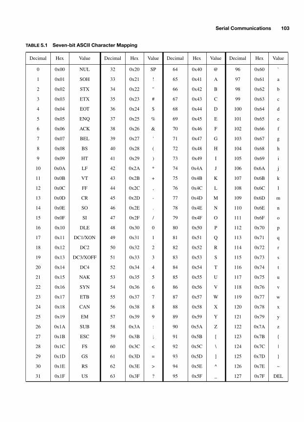
Serial Communications 103
TABLE
5.1 Seven-bit ASCII Character Mapping
Decimal Hex Value Decimal Hex Value Decimal Hex Value Decimal Hex Value
0 0x00 NUL 32 0x20 SP 64 0x40 @ 96 0x60 `
1 0x01 SOH 33 0x21 ! 65 0x41 A 97 0x61 a
2 0x02 STX 34 0x22 " 66 0x42 B 98 0x62 b
3 0x03 ETX 35 0x23 # 67 0x43 C 99 0x63 c
4 0x04 EOT 36 0x24 $ 68 0x44 D 100 0x64 d
5 0x05 ENQ 37 0x25 % 69 0x45 E 101 0x65 e
6 0x06 ACK 38 0x26 & 70 0x46 F 102 0x66 f
7 0x07 BEL 39 0x27 ' 71 0x47 G 103 0x67 g
8 0x08 BS 40 0x28 ( 72 0x48 H 104 0x68 h
9 0x09 HT 41 0x29 ) 73 0x49 I 105 0x69 i
10 0x0A LF 42 0x2A * 74 0x4A J 106 0x6A j
11 0x0B VT 43 0x2B + 75 0x4B K 107 0x6B k
12 0x0C FF 44 0x2C , 76 0x4C L 108 0x6C l
13 0x0D CR 45 0x2D - 77 0x4D M 109 0x6D m
14 0x0E SO 46 0x2E . 78 0x4E N 110 0x6E n
15 0x0F SI 47 0x2F / 79 0x4F O 111 0x6F o
16 0x10 DLE 48 0x30 0 80 0x50 P 112 0x70 p
17 0x11 DC1/XON 49 0x31 1 81 0x51 Q 113 0x71 q
18 0x12 DC2 50 0x32 2 82 0x52 R 114 0x72 r
19 0x13 DC3/XOFF 51 0x33 3 83 0x53 S 115 0x73 s
20 0x14 DC4 52 0x34 4 84 0x54 T 116 0x74 t
21 0x15 NAK 53 0x35 5 85 0x55 U 117 0x75 u
22 0x16 SYN 54 0x36 6 86 0x56 V 118 0x76 v
23 0x17 ETB 55 0x37 7 87 0x57 W 119 0x77 w
24 0x18 CAN 56 0x38 8 88 0x58 X 120 0x78 x
25 0x19 EM 57 0x39 9 89 0x59 Y 121 0x79 y
26 0x1A SUB 58 0x3A : 90 0x5A Z 122 0x7A z
27 0x1B ESC 59 0x3B ; 91 0x5B [ 123 0x7B
28 0x1C FS 60 0x3C < 92 0x5C \ 124 0x7C |
29 0x1D GS 61 0x3D = 93 0x5D ] 125 0x7D
30 0x1E RS 62 0x3E > 94 0x5E ^ 126 0x7E ~
31 0x1F US 63 0x3F ? 95 0x5F _ 127 0x7F DEL
-Balch.book Page 103 Thursday, May 15, 2003 3:46 PM

104 Digital Fundamentals
Standard bit rates are 2
N
multiples of 300 bps. In the 1970s, 300 bps serial links were common. Dur-ing the 1980s, links went from 1,200 to 2,400, to 9,600 bps. RS-232 data links now operate at speedsfrom 19.2 to 153.6 kbps. Standard RS-232 bit rates are typically divided down from reference clockssuch as 1.843, 3.6864, 6.144, and 11.0592 MHz. This explains why many microprocessors operateat oddball frequencies instead of even speeds such as 5, 10, or 12 MHz.
RS-232 defines signals from two different perspectives:
data communications equipment
(DCE)and
data terminal equipment
(DTE). DCE/DTE terminology evolved in the early days of computingwhen the common configuration was to have a dumb terminal attached to a modem of some sort toenable communication with a mainframe computer in the next room or building. A person would sitat the DTE and communicate via the DCE. Therefore, in the early 1960s, it made perfect sense tocreate a communication standard that specifically addressed this common configuration. By defininga set of DTE and DCE signals, not only could terminal and modem engineers design compatible sys-tems, but cabling would be very simple: just wire each DTE signal straight through to each DCE sig-nal. To further reduce confusion, the DTE was specified as a male DB-25 and the DCE as a femaleDB-25. Aside from transmit and receive data, hardware handshaking signals distinguish DCE fromDTE. Some signals are specific to modems such as
carrier detect
and
ring indicator
and are stillused today in many modem applications.
The principle behind RS-232 hardware handshaking is fairly simple: the DTE and DCE indicatetheir operational status and ability to accept data. The four main handshaking signals are
request tosend
(RTS),
clear to send
(CTS),
data terminal ready
(DTR), and
data set ready
(DSR). DTR/DSRenable the DTE and DCE to signal that they are both operational. The DTE asserts DTR, which issensed by the DCE and vice versa with DSR. RTS/CTS enable actual data transfer. RTS is assertedby the DTE to signal that the DCE can send it data. CTS is asserted by the DCE to signal the DTEthat it can send data. In the case of a modem, carrier detect is asserted to signal an active connection,and ring indicator is asserted when the telephone line rings, signaling that the DTE can instruct themodem to answer the phone.
In a
null-modem
configuration, two DTEs are connected, and each considers DTR and RTS out-puts and DSR and CTS inputs. This is solved by swapping DTR/DSR and RTS/CTS so that oneDTE’s DTR drives the other’s DSR, and so on. The unidirectional carrier detect is also connected tothe DTR signal at the other end (DSR at the local end) to provide positive “carrier detect” when theterminal ready signal is asserted.
Table 5.2 lists the full set of RS-232 signals with the convention that signals are named relative tothe DTE. Most of the original 25 defined RS-232 signals are rarely used, as evidenced by the popu-larity of the smaller DE9 connector. Furthermore, a minimal RS-232 serial link can be implementedwith only three wires: transmit, receive, and ground. In more recent times, the DTE/DCE distinctionhas created confusion in more than one engineering department, because the definitions of terminaland modem
do not always hold in the more varied modern digital systems context. Often, all RS-232ports are configured as DTE, and special crossover, or null-modem, cables are used to properly con-nect two DTEs. While varying subsets of the DTE pin assignment can be found in many systems,there is still a place for the original DTE/DCE configuration. It is rare, however, to find the DB25pins that are not implemented in the DE9 actually put to use.
Not all RS-232 interfaces are configured for hardware handshaking. Some may ignore these sig-nals entirely, and others require that these signals be tied off to the appropriate logic levels so thatneither end of the link gets confused and believes that the other is preventing it from sending data.Using a software flow control mechanism can eliminate the need for the aforementioned hardwarehandshaking signals and reduce the RS-232 link to its three basic wires: transmit, receive, andground. These many permutations of DTE/DCE and various degrees of handshaking are what causesubstantial grief to many engineers and technicians as they build and set up RS-232 equipment.There is a healthy industry built around the common RS-232 configuration problems.
Breakout
-Balch.book Page 104 Thursday, May 15, 2003 3:46 PM

Serial Communications 105
boxes
can be purchased that consist of jumper wires, switches, and LEDs to help troubleshoot RS-232 connectivity problems by reconfiguring interfaces on the fly as the LEDs indicate which signalsare active at any given moment. As a result of the male/female gender differences of various DB25/DE9 connectors, there are often cabling problems for which one needs to connect two males or twofemales together. Once again, the industry has responded by providing a broad array of gender-matching cables and adapters. On a conceptual level, these problems are simple; in practice, the per-
TABLE
5.2 RS-232 DTE Pin Assignments
DB25 DTE DE9 DTE Signal Direction: DTE/DCE Description
1 – Shield
⇔
Shield/chassis ground
2 3 TXD
⇒
Transmit data
3 2 RXD
⇐
Receive data
4 7 RTS
⇒
Request to send
5 8 CTS
⇐
Clear to send
6 6 DSR
⇐
Data set ready
7 5 Ground
⇔
Signal ground
8 1 DCD
⇐
Data carrier detect
9 – +V
⇔
Power
10 – –V
⇔
Power return
11 – Unused
12 – SCF
⇐
Secondary line detect
13 – SCB
⇐
Secondary CTS
14 – SBA
⇒
Secondary TXD
15 – DB
⇐
DCE element timing
16 – SBB
⇐
Secondary RXD
17 – DD
⇐
Receiver element timing
18 – Unused/local-loopback
19 – SCA
⇒
Secondary RTS
20 4 DTR
⇒
Data terminal ready
21 – CQ
⇐
Signal quality detect
22 9 RI
⇐
Ring indicator
23 – CH/CI
⇔
Data rate detect
24 – DA
⇒
Transmitter element timing
25 – Unused/test-mode
-Balch.book Page 105 Thursday, May 15, 2003 3:46 PM
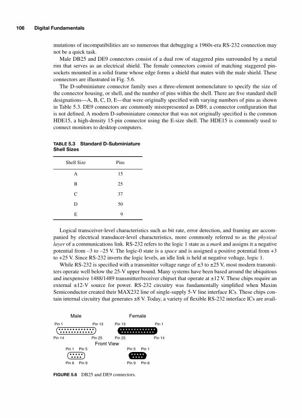
106 Digital Fundamentals
mutations of incompatibilities are so numerous that debugging a 1960s-era RS-232 connection maynot be a quick task.
Male DB25 and DE9 connectors consist of a dual row of staggered pins surrounded by a metalrim that serves as an electrical shield. The female connectors consist of matching staggered pin-sockets mounted in a solid frame whose edge forms a shield that mates with the male shield. Theseconnectors are illustrated in Fig. 5.6.
The D-subminiature connector family uses a three-element nomenclature to specify the size ofthe connector housing, or shell, and the number of pins within the shell. There are five standard shelldesignations—A, B, C, D, E—that were originally specified with varying numbers of pins as shownin Table 5.3. DE9 connectors are commonly misrepresented as DB9, a connector configuration thatis not defined. A modern D-subminiature connector that was not originally specified is the commonHDE15, a high-density 15-pin connector using the E-size shell. The HDE15 is commonly used toconnect monitors to desktop computers.
Logical transceiver-level characteristics such as bit rate, error detection, and framing are accom-panied by electrical transducer-level characteristics, more commonly referred to as the
physicallayer
of a communications link. RS-232 refers to the logic 1 state as a
mark
and assigns it a negativepotential from –3 to –25 V. The logic-0 state is a
space
and is assigned a positive potential from +3to +25 V. Since RS-232 inverts the logic levels, an idle link is held at negative voltage, logic 1.
While RS-232 is specified with a transmitter voltage range of ±3 to ±25 V, most modern transmit-ters operate well below the 25-V upper bound. Many systems have been based around the ubiquitousand inexpensive 1488/1489 transmitter/receiver chipset that operate at ±12 V. These chips require anexternal ±12-V source for power. RS-232 circuitry was fundamentally simplified when MaximSemiconductor created their MAX232 line of single-supply 5-V line interface ICs. These chips con-tain internal circuitry that generates ±8 V. Today, a variety of flexible RS-232 interface ICs are avail-
TABLE
5.3 Standard D-Subminiature Shell Sizes
Shell Size Pins
A 15
B 25
C 37
D 50
E 9
Front View
Pin 1
Pin 14
Pin 13
Pin 25
Pin 1 Pin 13
Pin 14 Pin 25
Male Female
Pin 1 Pin 5
Pin 6 Pin 9
Pin 1
Pin 6
Pin 5
Pin 9
FIGURE 5.6 DB25 and DE9 connectors.
-Balch.book Page 106 Thursday, May 15, 2003 3:46 PM

Serial Communications 107
able from other manufacturers including Linear Technology, National Semiconductor, and TexasInstruments. RS-232 ports work quite well on even lower voltage ranges, because modern receiversare sensitive to smaller absolute voltages, and most RS-232 links are several meters or less in length.RS-232 was never intended to serve in truly long-distance applications.
5.5 RS-422
For crossing distances greater than several meters, RS-232 is supplemented by the
RS-422
standard.RS-422 can provide communications across more than 1.2 km at moderate bit rates such as 9.6 kbps.It is a
differential
, or
balanced
, transmission scheme whereby each logical signal is represented bytwo wires rather than one. RS-232 signals are
single-ended
, or
unbalanced
, signals that drive a par-ticular voltage onto a single wire. This voltage is sensed at the receiver by measuring the signal volt-age relative to the ground potential of the interface. Over long distances or at very high speeds,single-ended transmission lines are more subject to degradation resulting from ambient electricalnoise. A partial explanation of this characteristic is that the electrical noise affects the active signalwire unequally with respect to ground. Differential signals, as in RS-422, drive opposing, or mir-rored, voltages onto two wires simultaneously (RS-422 is specified from ±2 to ±6 V). The receiverthen compares the voltages of the two wires together rather than to ground. Ambient noise tends toaffect the two wires equally, because they are normally twisted together to follow the same path.Therefore, if noise causes a 1-V spike on one-half of the differential pair, it causes the same spike onthe other half. When the two voltages are electrically subtracted at the receiver, the 1-V of
common-mode
noise cancels out, and the original differential voltage remains intact (subject, of course to nat-ural attenuation over distance). The difference between RS-232 and RS-422 transmission is illus-trated in Fig. 5.7.
Because of the longer distances involved in RS-422 interfaces, it is not common to employ thestandard set of hardware handshaking signals that are common with RS-232. Therefore, some formof software handshaking must be implemented by the end devices to properly communicate. Someapplications may not require any flow control, and some may use the XON/XOFF method. RS-422does not specify a standard connector. It is not uncommon to see an RS-422 transmission line’s barewire ends connected to screw terminals.
Another common difference between RS-422 and RS-232 is transmission line
termination
. Trans-mission line theory can get rather complicated and is outside the scope of this immediate discussion.
Tx Rx+V
TX+V
RX
Tx Rx
+VTX
RS-232
–VTX
+VRX
–VRX
RS-422
VSENSE
= +VRX
- ground
VSENSE
= +VRX
- –VRX
FIGURE 5.7 RS-232 vs. RS-422 signaling.
-Balch.book Page 107 Thursday, May 15, 2003 3:46 PM

108 Digital Fundamentals
The basic practical result of transmission line theory is that, as the speed-distance product of an elec-trical signal increases, the signal tends to reflect off the ends of wires and bounce back and forth onthe wire. When slow signals travel relatively moderate distances, the speed-distance product is notlarge enough to cause this phenomenon to any noticeable degree. Fast signals traveling over veryshort distances may also be largely immune to such reflections. However, when RS-422 signalstravel over several kilometers, the speed-bandwidth product is great enough to cause previouslytransmitted data signals to reflect and interfere with subsequent data. This problem can be largelysolved by properly
terminating
the receiving end of the transmission line with the line’s
characteris-tic impedance
, Z
O
. Typical coaxial and twisted-pair transmission lines have Z
O
= 50, 75, or 110
Ω
.Briefly put, Z
O
is the impedance, or electrical resistance, that would be observed between both con-ductors of a balanced transmission line of infinite length. Again, there is substantial theory lurkinghere, but the practical result is that, by placing a resistor equal to Z
O
at the far end of the line be-tween both conductors, the transmission line will appear to be continuous and not exhibit reflections.A typical schematic diagram of a terminated RS-422 serial link is shown in Fig. 5.8.
5.6 MODEMS AND BAUD RATE
Information is conveyed by varying the electromagnetic field of a particular medium over time. Therate at which this field (e.g., voltage) changes can be represented by a certain bandwidth that charac-terizes the information. Transducers such as those that facilitate RS-232/RS-422 serial links placethe information that is presented to them essentially unmodified onto the transmission medium. Inother words, the bandwidth of the information entering the transducer is equivalent to that leavingthe transducer. Such a system operates at
baseband:
the bandwidth inherent to the raw information.Baseband operation is relatively simple and works well for a transmission medium that can carryraw binary signals with minimal degradation (e.g., various types of wire, or fiber optic cable, strungdirectly from transmitter to receiver). However, there are many desirable communications media thatare not well suited to directly carrying bits from one point to another. Two prime examples are free-space and acoustic media such as a telephone.
To launch raw information into the air or over a telephone, the bits must be superimposed upon a
carrier
that is suited to the particular medium. A carrier is a frequency that can be efficiently radi-ated from a transmitter and detected by a remote receiver. The process of superimposing the bits onthe carrier is called
modulation
. The reverse process of detecting the bits already modulated onto thecarrier is
demodulation
. For the purposes of this discussion, one of the simplest forms of modula-tion, binary
amplitude modulation
(AM), is presented as an example. More precisely, this type ofAM is called
amplitude shift keying
(ASK). With two states, it is called 2-ASK and is illustrated inFig. 5.9. Each time a 1 is to be transmitted, the carrier (shown as a sine wave of arbitrary frequency)is turned on with an arbitrary amplitude. Each time a 0 is to be transmitted, the carrier is turned offwith an amplitude of zero. If transmitting over free space, the carrier frequency might be anywherefrom hundreds of kilohertz to gigahertz. If communicating over a fiber optic cable, the carrier is
Tx
ZO =110 Ω
Rx
RT=110 Ω
FIGURE 5.8 RS-422 transmission line termination.
-Balch.book Page 108 Thursday, May 15, 2003 3:46 PM

Serial Communications 109
light. If an acoustic medium such as a telephone is used to send the data, the carrier is audible in therange of several kilohertz.
Frequency shift keying
(FSK), a type of
frequency modulation
(FM) is a scheme that can be usedto transmit multiple bits simultaneously without resorting to multiple levels of amplitude by usingAM. FSK represents multiple bits by varying the frequency rather than the amplitude of the carrier.This constant amplitude approach is less susceptible to noise. Figure 5.10 shows 4-FSK modulation,in which each of the four frequency steps represents a different two-digit binary value.
A general term for a modulated data unit is a
baud
. If 2-ASK is used, each baud corresponds toone bit. Therefore, the baud rate matches the bit rate. However, the 4-FSK example shows that eachbaud represents two bits, making the bit rate twice that of the baud rate. This illustrates that baudrate and bit rate are related but not synonymous, despite common misuse in everyday conversation.Engineers who design modulation circuitry care about the baud rate, because it specifies how manyunique data units can be transmitted each second. They also try to squeeze as many bits per baud aspossible to maximize the overall bit rate of the modulator. Engineers who use modulators as black-box components do not necessarily care about the baud rate; rather, it is the system’s bit rate thatmatters to the end application.
Enter the
modem
. A modem is simply a device that incorporates a modulator and demodulator fora particular transmission medium. The most common everyday meaning of modem is one that en-ables a computer to transfer bits over an analog telephone line. These modems operate using differ-ent modulation schemes depending on their bit rate. Early 300- and 1,200-bps modems operateusing FSK and
phase shift keying
(PSK). Later modems, including today’s 33.6- and 56-kbps mod-els, operate using variations of
quadrature amplitude modulation
(QAM).While
modem
often refers to telephone media, it is perfectly correct to use this term when refer-ring to a generic modulator/demodulator circuit that operates on another medium. Digital wirelesscommunication is increasingly common in such applications as portable cellular phones and unteth-ered computer networking. These devices incorporate radio frequency (RF) modems in addition todigital transceivers that frame the data as it travels from one point to another.
5.7 NETWORK TOPOLOGIES
The communications schemes discussed thus far are point-to-point connections—they involve onetransmitter and one receiver at either end of a given medium. Many applications require multidropcommunications whereby multiple devices exchange data over the same medium. The general term
"1" "0" "1" "1"
FIGURE 5.9 2-ASK modulation.
"00" "01" "10" "11"
FIGURE 5.10 4-FSK modulation.
-Balch.book Page 109 Thursday, May 15, 2003 3:46 PM
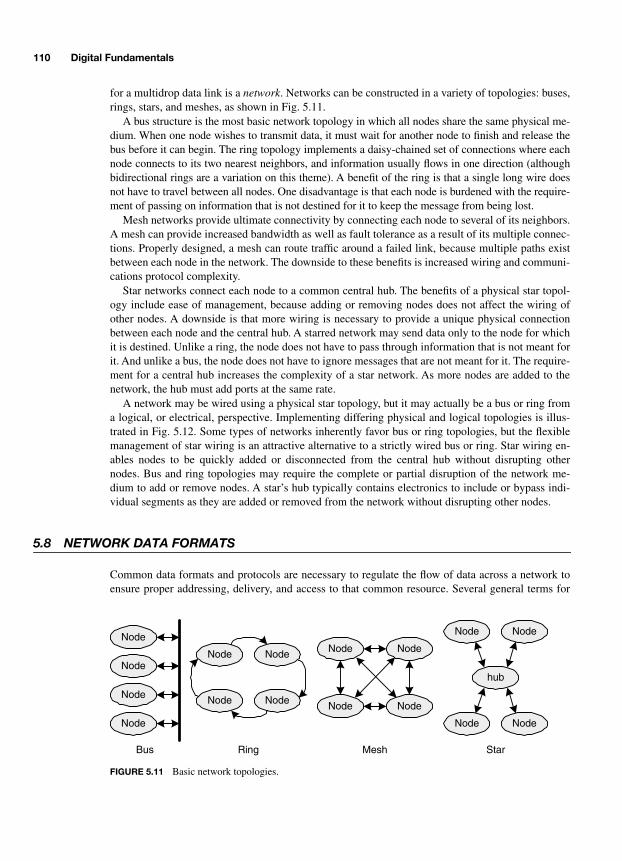
110 Digital Fundamentals
for a multidrop data link is a network. Networks can be constructed in a variety of topologies: buses,rings, stars, and meshes, as shown in Fig. 5.11.
A bus structure is the most basic network topology in which all nodes share the same physical me-dium. When one node wishes to transmit data, it must wait for another node to finish and release thebus before it can begin. The ring topology implements a daisy-chained set of connections where eachnode connects to its two nearest neighbors, and information usually flows in one direction (althoughbidirectional rings are a variation on this theme). A benefit of the ring is that a single long wire doesnot have to travel between all nodes. One disadvantage is that each node is burdened with the require-ment of passing on information that is not destined for it to keep the message from being lost.
Mesh networks provide ultimate connectivity by connecting each node to several of its neighbors.A mesh can provide increased bandwidth as well as fault tolerance as a result of its multiple connec-tions. Properly designed, a mesh can route traffic around a failed link, because multiple paths existbetween each node in the network. The downside to these benefits is increased wiring and communi-cations protocol complexity.
Star networks connect each node to a common central hub. The benefits of a physical star topol-ogy include ease of management, because adding or removing nodes does not affect the wiring ofother nodes. A downside is that more wiring is necessary to provide a unique physical connectionbetween each node and the central hub. A starred network may send data only to the node for whichit is destined. Unlike a ring, the node does not have to pass through information that is not meant forit. And unlike a bus, the node does not have to ignore messages that are not meant for it. The require-ment for a central hub increases the complexity of a star network. As more nodes are added to thenetwork, the hub must add ports at the same rate.
A network may be wired using a physical star topology, but it may actually be a bus or ring froma logical, or electrical, perspective. Implementing differing physical and logical topologies is illus-trated in Fig. 5.12. Some types of networks inherently favor bus or ring topologies, but the flexiblemanagement of star wiring is an attractive alternative to a strictly wired bus or ring. Star wiring en-ables nodes to be quickly added or disconnected from the central hub without disrupting othernodes. Bus and ring topologies may require the complete or partial disruption of the network me-dium to add or remove nodes. A star’s hub typically contains electronics to include or bypass indi-vidual segments as they are added or removed from the network without disrupting other nodes.
5.8 NETWORK DATA FORMATS
Common data formats and protocols are necessary to regulate the flow of data across a network toensure proper addressing, delivery, and access to that common resource. Several general terms for
Node
Node Node
Node
hub
Star
Node
Node Node
Node
Mesh
Node
Node
Node
Node
Bus
Node Node
Node Node
Ring
FIGURE 5.11 Basic network topologies.
-Balch.book Page 110 Thursday, May 15, 2003 3:46 PM

Serial Communications 111
message elements on a network are frame, packet, and cell. Frames are sets of data that are framed atthe beginning and end by special delimiters. Packets are sets of data that are not fully framed but thathave some other means of determining their size, such as an embedded length field. Cells are fixed-length frames or packets. Frames and packets usually imply variable length data sets, but this is not astrict rule. As with many terms and classifications in digital systems, specific definitions are contextspecific and are often blurred: one system’s cells may be another’s frames. Frames, packets, andcells are composed of headers, payloads, and trailers, as shown in Fig. 5.13. The header is a collec-tion of data fields that handle network overhead functions such as addressing and delineation. Theactual data to be transmitted is placed into the payload. If present, a trailer is commonly used to im-plement some form of error checking and/or delineation. Not all packet formats specify the inclusionof trailers. When present, a trailer is usually substantially smaller in length than the header.
Networking is an aspect of digital systems design that directly involves hardware–software inter-action at a basic level. One cannot really design networking hardware without keeping in mind theprotocol, or software, support requirements. One key example is packet format. Hardware must haveknowledge of the packet format so that it can properly detect a packet that is sent to it. At the sametime, software must have this same knowledge so that it can properly parse received packets andgenerate new ones to be transmitted.
As soon as more than two nodes are connected to form a network, issues such as addressing andshared access arise. When there is only one transmitter and one receiver, it is obvious that data is in-tended for the only possible recipient. Likewise, the lone transmitter can begin sending data at anytime it chooses, because there are no other transmitters competing for network access.
Network addressing is the mechanism by which a transmitting node indicates the destination forits packet. Each node on the network must therefore have a unique address to prevent confusion overwhere the packet should be delivered. In a bus topology, each node watches all the data traffic that isplaced onto the network and picks out those packets that are tagged with its unique address. In a ringtopology, each node passes packets on to the next node if the destination address is not matched withthat node’s address. If the address is matched, the node absorbs the packet and does not forward it onto the next node in the ring. Logical star and mesh topologies function a bit differently. Nodes on
Logical Bus
Node
Node Node
Node
hubhub
Logical Ring
Node
Node
Node
Node
FIGURE 5.12 Physical vs. logical network topologies.
Header TrailerPayload
FIGURE 5.13 Generic packet structure.
-Balch.book Page 111 Thursday, May 15, 2003 3:46 PM

112 Digital Fundamentals
these types of networks do not observe all traffic that traverses the network; rather, the network itselfcontains some intelligence when it comes to delivering a packet. A node in a logically starred net-work sends a packet to a central hub that examines the destination address and then forwards themessage to only the specified node. A mesh network routes traffic partly like a ring and partly like astar; however, multiple paths between nodes exist to complicate the delivery process. Based on thedestination address, the originating node sends a packet to one of its neighbors, which in turn for-wards the message to one of its neighbors. This process continues until the path has been completedand the packet arrives at its intended destination. The presence of multiple valid paths betweennodes requires the mesh network to use knowledge about the location of nodes to select an optimalpath through the network.
Access sharing is necessary on networks to ensure that each node eventually has an opportunity tosend a message. Numerous methods of access sharing have been implemented over the years. Gen-erally speaking, the length of messages is bounded to prevent a node from transmitting an infinitelylong set of data and preventing anyone else from gaining access to the shared medium. Sharing algo-rithms differ according to the specific network topology involved. Networks that are a collection ofpoint-to-point links (e.g., ring, star, mesh) do not have to worry about multiple nodes fighting for ac-cess to the same physical wire, but do have to ensure that one node does not steal all the bandwidthfrom others. Bus networks require sharing algorithms that address both simultaneous physical con-tention for the same shared wire in addition to logical contention for the network’s bandwidth. Arbi-tration schemes can be centralized (whereby a single network master provides permission to eachnode to transmit) or distributed (whereby each node cooperates on a peer-to-peer level to resolve si-multaneous access attempts).
After deciding on a network topology, one of the first issues to resolve is the network packet for-mat. If the network type is already established (e.g., Ethernet), the associated formats and protocolsare already defined by industry and government standards committees. If an application benefits froma simple, custom network, the packet format can be tailored to suit the application’s specific needs.
Delineation and addressing are the two most basic issues to resolve. Delineation can be accom-plished by sending fixed-size packets, embedding a length field in the packet header, or by reservingunique data values to act as start/stop markers. Framing with unique start/stop codes places a restric-tion on the type of data that a packet can contain: it cannot use these unique codes without causingfalse start or end indications. Referring back to Table 5.1, notice that start-of-header (SOH) and end-of-transmission (EOT) are represented by 0x01 and 0x04. These (or other pairs of codes) can beused as delimiters if the packet is guaranteed to contain only alphanumeric ASCII values that do notconflict with these codes.
Addressing is normally achieved by inserting both the destination and source addresses into theheader. However, some networking schemes may send only a single address. Sending both addressesenables recognition of the destination as well as a determination of which node sent the packet. Sincemost data exchanges are bidirectional to a certain degree, a destination node will probably need to sendsome form of reply to the source node of a particular packet. Many networks include a provision knownas broadcast addressing whereby a packet is sent to all nodes on the network rather than just one. Thisbroadcast is often indicated using a reserved broadcast address. In contrast to a unicast address that ismatched by only one node, a broadcast address is matched by all nodes on the network. Some networksalso have multicast addresses that associate multiple nodes with a single destination address.
5.9 RS-485
Whereas RS-232 and RS-422 enable point-to-point serial links, the RS-485 standard enables multi-ple-node networks. Like RS-422, RS-485 provides differential signaling to enable communications
-Balch.book Page 112 Thursday, May 15, 2003 3:46 PM
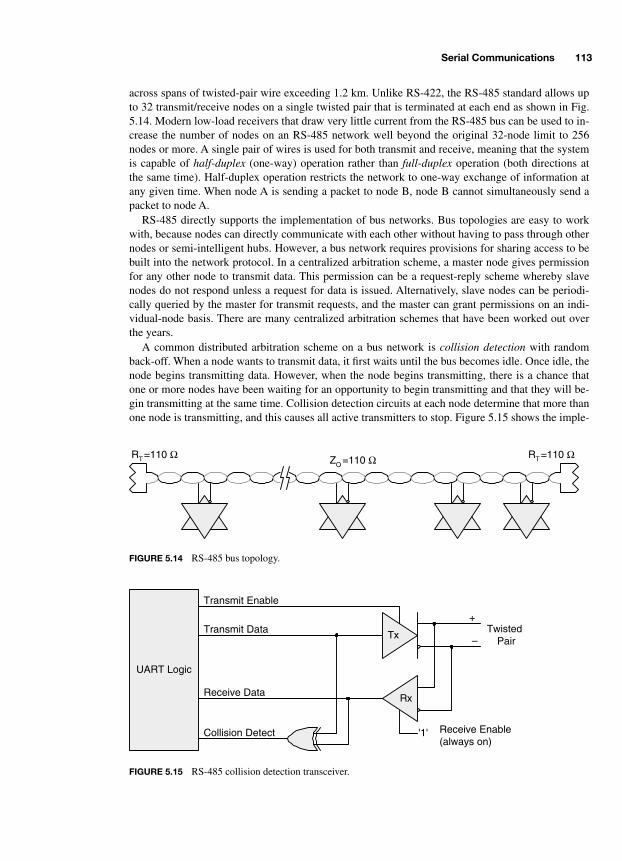
Serial Communications 113
across spans of twisted-pair wire exceeding 1.2 km. Unlike RS-422, the RS-485 standard allows upto 32 transmit/receive nodes on a single twisted pair that is terminated at each end as shown in Fig.5.14. Modern low-load receivers that draw very little current from the RS-485 bus can be used to in-crease the number of nodes on an RS-485 network well beyond the original 32-node limit to 256nodes or more. A single pair of wires is used for both transmit and receive, meaning that the systemis capable of half-duplex (one-way) operation rather than full-duplex operation (both directions atthe same time). Half-duplex operation restricts the network to one-way exchange of information atany given time. When node A is sending a packet to node B, node B cannot simultaneously send apacket to node A.
RS-485 directly supports the implementation of bus networks. Bus topologies are easy to workwith, because nodes can directly communicate with each other without having to pass through othernodes or semi-intelligent hubs. However, a bus network requires provisions for sharing access to bebuilt into the network protocol. In a centralized arbitration scheme, a master node gives permissionfor any other node to transmit data. This permission can be a request-reply scheme whereby slavenodes do not respond unless a request for data is issued. Alternatively, slave nodes can be periodi-cally queried by the master for transmit requests, and the master can grant permissions on an indi-vidual-node basis. There are many centralized arbitration schemes that have been worked out overthe years.
A common distributed arbitration scheme on a bus network is collision detection with randomback-off. When a node wants to transmit data, it first waits until the bus becomes idle. Once idle, thenode begins transmitting data. However, when the node begins transmitting, there is a chance thatone or more nodes have been waiting for an opportunity to begin transmitting and that they will be-gin transmitting at the same time. Collision detection circuits at each node determine that more thanone node is transmitting, and this causes all active transmitters to stop. Figure 5.15 shows the imple-
ZO =110 ΩRT=110 Ω RT=110 Ω
FIGURE 5.14 RS-485 bus topology.
Tx
Rx
+
–Twisted
Pair
Transmit Enable
Receive Enable(always on)
Transmit Data
Receive Data
UART Logic
Collision Detect '1'
FIGURE 5.15 RS-485 collision detection transceiver.
-Balch.book Page 113 Thursday, May 15, 2003 3:46 PM

114 Digital Fundamentals
mentation of an RS-485 transceiver with external collision detection logic. A transmit enable signalexists to turn off the transmitter when the UART is not actively sending data. Unlike an RS-422transmitter that does not have to share access with others, the RS-485 transmitter must turn itself offwhen not sending data to enable others to transmit.
When transmitting, the receiver returns the logical state of the twisted-pair bus. If the bus is not atthe same state as the transmitted data, a collision is most likely being caused by another transmittertrying to drive the opposite logic state. An XOR gate implements this collection detect, and the XORoutput must be sampled only after allowing adequate time for the bus to settle to a stable state fol-lowing the assertion of each bit from the transmitter.
Once a collision has been detected by each node and the transmitters are disabled, each nodewaits a different length of time before retransmitting. If all delays were equal, multiple nodes wouldget caught in a deadlock situation wherein each node keeps trying to transmit after the same delayinterval. Random back-off delays are pseudo-random so as to not unfairly burden some nodes withconsistently longer delays than other nodes. At the end of the delay, one of the nodes begins trans-mitting first and gains control of the bus by default. The other waiting nodes eventually exit fromtheir delays and observe that the bus is already busy, indicating that they must wait their turn untilthe current packet has been completed. If, by coincidence, another node begins transmitting at thesame time that the first node begins, the back-off process begins again. It is statistically possible forthis process to occur several times in a row, although the probability of this being a frequent event issmall in a properly designed network. A bus network constructed with too many nodes trying to sendtoo much data at the same time can exhibit very poor performance, because it would be quite proneto collisions. In such a case, the solution may be to either reduce the network traffic or increase thenetwork’s bandwidth.
5.10 A SIMPLE RS-485 NETWORK
An example of a simple but effective network implemented with RS-485 serves as a vehicle to dis-cuss how packet formats, protocols, and hardware converge to yield a useful communications me-dium. The motivation to create a custom RS-485 network often arises from a need to deploy remoteactuators and data-acquisition modules in a factory or campus setting. A central computer may be lo-cated in a factory office, and it may need to periodically gather process information (e.g., tempera-ture, pressure, fluid-flow rate) from a group of machines. Alternatively, a security control consolelocated in one building may need to send security camera positioning commands to locationsthroughout the campus. Such applications may involve a collection of fairly simple and inexpensivemicroprocessor-based modules that contain RS-485 transceivers. Depending on the exact physicallayout, it may or may not be practical to wire all remote nodes together in a single twisted-pair bus.If not, a logical bus can be formed by creating a hybrid star/bus topology as shown in Fig. 5.16. Acentral hub electrically connects the individual star segments so that they function electrically as alarge bus but do not require a single wire to be run throughout the entire campus.
As shown, the hub does not contain any intelligent components—it is a glorified junction box.This setup is adequate if the total length of all star segments does not exceed 1.2 km, which is withinthe electrical limitations of the RS-485 standard. While simple, this setup suffers from a lack of faulttolerance. If one segment of the star wiring is damaged, the entire network may cease operation be-cause, electrically, it is a single long pair of wires. Both the distance and fault-tolerance limitationscan be overcome by implementing an active hub that contains repeaters on each star segment andsmart switching logic to detect and isolate a broken segment. A repeater is an active two-port devicethat amplifies or regenerates the data received on one port and transmits it on the other port. An RS-
-Balch.book Page 114 Thursday, May 15, 2003 3:46 PM

Serial Communications 115
485 repeater needs a degree of intelligence, because both ports must be bidirectional. Therefore, therepeater must be able to listen for traffic on both sides, detect traffic on one side, and then transmitthat traffic on the other side. A hub that detects and isolates segment failures would be well designedto report this fault information to a central control node to alert the human operator that repairs arenecessary. These possible improvements in the network hub do not affect the logical operation of thenetwork and, consequently, are not a focus of this discussion.
With a topology chosen and a general application in mind, the next step is to decide on the net-work’s operational requirements from among the following:
1. Support for roughly 200 nodes provides flexibility for a variety of control applications.
2. Central arbitration handled by master control node for simplicity of network design. A facilitycontrol network is often a master-slave application, because all data transfers are at the requestof the central controller. Central arbitration removes the need for collision-detect hardware andrandom back-off algorithms.
3. Broadcast capability enables easy distribution of network status information from the mastercontrol node.
4. Data rate of 9600 bps provides adequate bandwidth for small control messages without burden-ing the network with high frequencies that can lead to excessive noise and signal degradation.
5. Basic error handling prevents processing incorrect data and network lock-up conditions whenoccasional noise on the RS-485 twisted-pairs causes data bits to change state.
Many aspects of network functionality are directly influenced by a suitable network packet for-mat. Other aspects are addressed by the protocol that formats data on the network, by the transceiverand UART hardware, or by a combination of these three elements.
In considering the packet format, 8-bit destination and source addresses are chosen to supportmore than 200 nodes on the network. A special destination address value of 0xFF represents a broad-cast address, meaning that all nodes should accept the packet automatically. Such broadcast packetsare useful for system-wide initialization whereby, for example, the control computer can send thecurrent time to all nodes. This multicast address cannot be used as a normal node address, therebylimiting the network to 255 unique nodes.
It is desirable to employ variable-length packets so that a message does not have to be longer thannecessary, thereby conserving network bandwidth. Variable-length packets require some mechanism
Node
Node
Node
hub
Node
Node
Node
Node
NodeNode
Node
FIGURE 5.16 Hybrid star/bus network topology.
-Balch.book Page 115 Thursday, May 15, 2003 3:46 PM
116 Digital Fundamentals
to determine the length: either reserved framing codes or an explicit length count. A length count ischosen to keep the system simple. Framing codes would require that certain data values be off limitsto the contents of the message. The payload length is bounded at a convenient binary threshold: 255bytes. For simple control and data-acquisition applications, this is probably more than enough.
Based on these basic requirements and a couple of quick decisions, a packet format quicklyemerges. A three-byte, fixed-length header shown in Table 5.4 is followed by a variable-length pay-load. No trailer is necessary in this network.
The eight-bit destination address field, DA, comes first to enable the receiving hardware toquickly determine whether the packet should be accepted by the node or ignored. A packet will beaccepted if DA matches the receiver’s node address, or if DA equals 0xFF, indicating a broadcastpacket. At the end of the header is an eight-bit length field that indicates how many payload bytes arepresent after the fixed-length header. This limits the maximum packet size to 255 payload bytes plusthe 3-byte header. A value of zero means that there is no payload, only a header in the packet.
Error detection can be handled by even parity. Each byte of the header and payload is sent with anaccompanying parity bit. When an error is detected, the network’s behavior must be clearly definedto prevent the system from either ceasing to function or acting on false data. Parity errors can mani-fest themselves in a variety of tricky ways. For example, if the length field has a parity error, howwill the receiver know the true end of the frame? Without proper planning, a parity error on thelength field can permanently knock the receivers out of sync and make automatic recovery impossi-ble. This extreme situation can occur when an invalid length causes the receiver to either skip overthe next frame header or prematurely interpret the end of the current frame as a new header. In bothcases, the receiver will falsely interpret a bogus length field, and the cycle of false header detectioncan continue indefinitely.
If a parity error is detected on either the destination or source addresses, the receivers will not losesynchronization, but the packet should be ignored, because it cannot be known who the true recipi-ent or sender of the packet is.
Fault tolerance in the case of an invalid payload length can be handled in a relatively simple man-ner. Requirements of no intrapacket gaps and a minimum interpacket gap assist in recovery fromlength-field parity errors. The absence of intrapacket gaps means that, once a packet has begun trans-mission, its bytes must be continuous without gaps. Related to this is the requirement of a minimuminterpacket gap which forces a minimum idle period between the last byte of one packet and the startof the next packet. These requirements help each receiver determine when packets are starting andending. Even if a packet has been subjected to parity errors, the receiver can wait until the currentburst of traffic has ended, wait for the minimum interpacket gap, and then begin looking for the nextpacket to begin.
The parity error detection and accompanying recovery scheme greatly increases the probabilitythat false data will not be acted upon as correct data and that the entire network will not stop func-tioning when it encounters an arbitrary parity error. However, error detection is all about probability.
TABLE 5.4 Hypothetical Packed Header Format
Field Name Byte Bits Description
DA 0 [7:0] Destination address (0xFF = multicast)
SA 1 [7:0] Source address
LEN 2 [7:0] Payload length (0x0 = no payload present)
-Balch.book Page 116 Thursday, May 15, 2003 3:46 PM
Serial Communications 117
A single parity bit cannot guarantee the detection of multiple errors in the same byte, because sucherrors can mask themselves. For example, two bit errors can flip a data bit and the parity bit itself,making it impossible for the receiver to detect the error. More complex error detection schemes areavailable and are more difficult to fool. Although no error detection solution is perfect, someschemes reduce the probability of undetected errors to nearly zero.
If a packet is received with an error, it cannot be acted upon normally, because its contents aresuspect. For the purposes of devising a useful error-handling scheme, packet errors can be dividedinto two categories: those that corrupt the destination/source address information and those that donot. Parity errors that corrupt the packet’s addresses must result in the packet being completely ig-nored, because the receiving node is unable to generate a reply message to the originator indicatingthat the packet was corrupted. If the source address is corrupted, the receiver does not know to whomto reply. If the destination address is corrupted, the receiver does not know whether it is the indentedrecipient.
In the case of an address error in which the received packet is ignored, the originator must imple-ment some mechanism to recover from the packet loss rather than waiting indefinitely for a replythat will never arrive. A reply timeout can be implemented by an originator each time a packet is sentthat requires a corresponding reply. A timeout is an arbitrary delay during which an originating nodewaits before giving up on a response from a remote node. Timeouts are common in networks be-cause, if a packet is lost due to an error, the originator should not wait indefinitely for a response thatwill never come. Establishing a timeout value is a compromise between not giving up too quicklyand missing a slower-than-normal reply and waiting too long and introducing unacceptable delays insystem functionality when a packet is lost. Depending on the time it takes to send a packet on a net-work and the nodes’ typical response time, timeouts can range from microseconds to minutes. Typi-cal timeouts are often expressed in milliseconds.
When an originator times-out and concludes that its requested data somehow got lost, it can re-send the request. If, for example, a security control node sends a request for a camera to pan across aroom, and that request is not acknowledged within half a second, the request can be retransmitted.
In the case of a non-address error, the receiving node has enough information to send a reply backto the originator, informing it that the packet was not correctly received. Such behavior is desirableto enable the originator to retransmit the packet rather than waiting for a timeout before resendingthat data.
The preceding details of a hypothetical RS-485 network must be gathered into network driversoftware to enable proper communication across the network. While hardware controls the detectionof parity errors and the flow of bits, it is usually software that generates reply messages and countsdown timeouts. Figure 5.17 distills this information into a single flowchart from which software rou-tines could be written.
As seen from this flowchart, transmit and receive processes run concurrently and are related. Thetransmit process does not complete until a positive acknowledgement is received from the destina-tion node. This network control logic implemented in software is simple by mainstream networkingstandards, yet it is adequate for networks of limited size and complexity. Issues such as access shar-ing are handled inherently by the request/reply nature of this network, greatly simplifying the trafficpatterns that must be handled by the software driver.
5.11 INTERCHIP SERIAL COMMUNICATIONS
Serial data links are not always restricted to long-distance communications. Within a single com-puter system, or even a single circuit board, serial links can provide attractive benefits as compared
-Balch.book Page 117 Thursday, May 15, 2003 3:46 PM
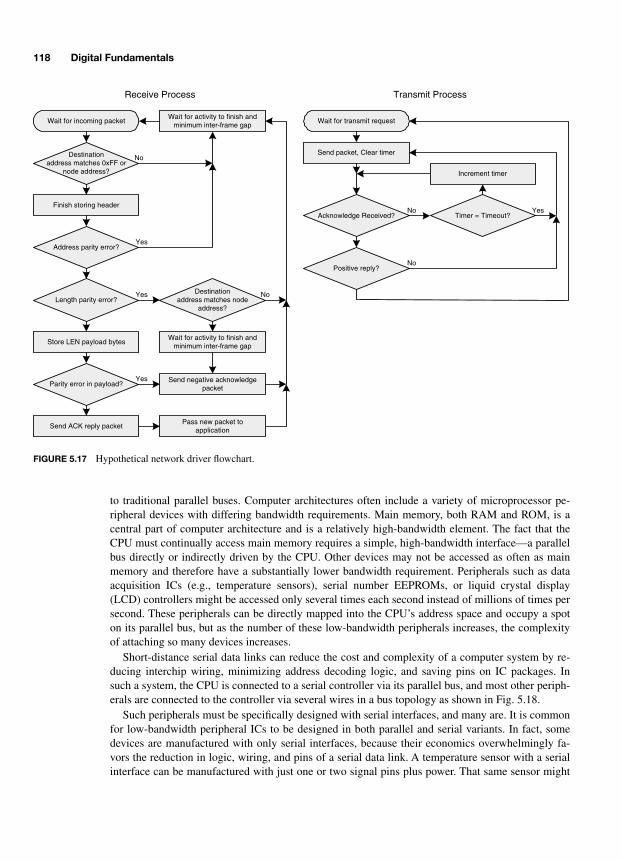
118 Digital Fundamentals
to traditional parallel buses. Computer architectures often include a variety of microprocessor pe-ripheral devices with differing bandwidth requirements. Main memory, both RAM and ROM, is acentral part of computer architecture and is a relatively high-bandwidth element. The fact that theCPU must continually access main memory requires a simple, high-bandwidth interface—a parallelbus directly or indirectly driven by the CPU. Other devices may not be accessed as often as mainmemory and therefore have a substantially lower bandwidth requirement. Peripherals such as dataacquisition ICs (e.g., temperature sensors), serial number EEPROMs, or liquid crystal display(LCD) controllers might be accessed only several times each second instead of millions of times persecond. These peripherals can be directly mapped into the CPU’s address space and occupy a spoton its parallel bus, but as the number of these low-bandwidth peripherals increases, the complexityof attaching so many devices increases.
Short-distance serial data links can reduce the cost and complexity of a computer system by re-ducing interchip wiring, minimizing address decoding logic, and saving pins on IC packages. Insuch a system, the CPU is connected to a serial controller via its parallel bus, and most other periph-erals are connected to the controller via several wires in a bus topology as shown in Fig. 5.18.
Such peripherals must be specifically designed with serial interfaces, and many are. It is commonfor low-bandwidth peripheral ICs to be designed in both parallel and serial variants. In fact, somedevices are manufactured with only serial interfaces, because their economics overwhelmingly fa-vors the reduction in logic, wiring, and pins of a serial data link. A temperature sensor with a serialinterface can be manufactured with just one or two signal pins plus power. That same sensor might
Wait for incoming packetWait for activity to finish and
minimum inter-frame gap
Destinationaddress matches 0xFF or
node address?
Finish storing header
Address parity error?
Store LEN payload bytes
Parity error in payload?Send negative acknowledge
packet
Send ACK reply packetPass new packet to
application
No
Yes
Yes
Wait for transmit request
Send packet, Clear timer
Acknowledge Received?No
Receive Process Transmit Process
Timer = Timeout?
Increment timer
Yes
Positive reply?No
Length parity error?Yes
Wait for activity to finish andminimum inter-frame gap
Destinationaddress matches node
address?
No
FIGURE 5.17 Hypothetical network driver flowchart.
-Balch.book Page 118 Thursday, May 15, 2003 3:46 PM
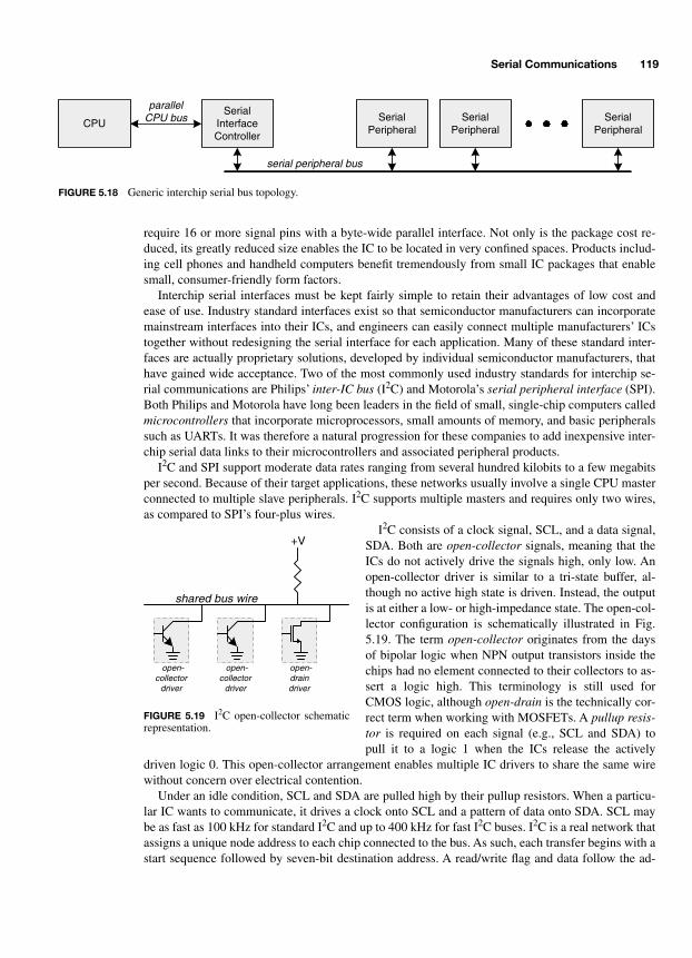
Serial Communications 119
require 16 or more signal pins with a byte-wide parallel interface. Not only is the package cost re-duced, its greatly reduced size enables the IC to be located in very confined spaces. Products includ-ing cell phones and handheld computers benefit tremendously from small IC packages that enablesmall, consumer-friendly form factors.
Interchip serial interfaces must be kept fairly simple to retain their advantages of low cost andease of use. Industry standard interfaces exist so that semiconductor manufacturers can incorporatemainstream interfaces into their ICs, and engineers can easily connect multiple manufacturers’ ICstogether without redesigning the serial interface for each application. Many of these standard inter-faces are actually proprietary solutions, developed by individual semiconductor manufacturers, thathave gained wide acceptance. Two of the most commonly used industry standards for interchip se-rial communications are Philips’ inter-IC bus (I2C) and Motorola’s serial peripheral interface (SPI).Both Philips and Motorola have long been leaders in the field of small, single-chip computers calledmicrocontrollers that incorporate microprocessors, small amounts of memory, and basic peripheralssuch as UARTs. It was therefore a natural progression for these companies to add inexpensive inter-chip serial data links to their microcontrollers and associated peripheral products.
I2C and SPI support moderate data rates ranging from several hundred kilobits to a few megabitsper second. Because of their target applications, these networks usually involve a single CPU masterconnected to multiple slave peripherals. I2C supports multiple masters and requires only two wires,as compared to SPI’s four-plus wires.
I2C consists of a clock signal, SCL, and a data signal,SDA. Both are open-collector signals, meaning that theICs do not actively drive the signals high, only low. Anopen-collector driver is similar to a tri-state buffer, al-though no active high state is driven. Instead, the outputis at either a low- or high-impedance state. The open-col-lector configuration is schematically illustrated in Fig.5.19. The term open-collector originates from the daysof bipolar logic when NPN output transistors inside thechips had no element connected to their collectors to as-sert a logic high. This terminology is still used forCMOS logic, although open-drain is the technically cor-rect term when working with MOSFETs. A pullup resis-tor is required on each signal (e.g., SCL and SDA) topull it to a logic 1 when the ICs release the actively
driven logic 0. This open-collector arrangement enables multiple IC drivers to share the same wirewithout concern over electrical contention.
Under an idle condition, SCL and SDA are pulled high by their pullup resistors. When a particu-lar IC wants to communicate, it drives a clock onto SCL and a pattern of data onto SDA. SCL maybe as fast as 100 kHz for standard I2C and up to 400 kHz for fast I2C buses. I2C is a real network thatassigns a unique node address to each chip connected to the bus. As such, each transfer begins with astart sequence followed by seven-bit destination address. A read/write flag and data follow the ad-
CPUSerial
InterfaceController
parallelCPU bus Serial
PeripheralSerial
PeripheralSerial
Peripheral
serial peripheral bus
FIGURE 5.18 Generic interchip serial bus topology.
open-collector
driver
open-draindriver
open-collector
driver
+V
shared bus wire
FIGURE 5.19 I2C open-collector schematicrepresentation.
-Balch.book Page 119 Thursday, May 15, 2003 3:46 PM
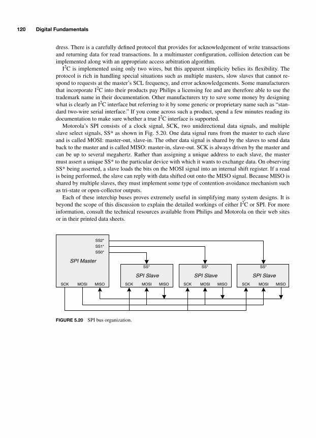
120 Digital Fundamentals
dress. There is a carefully defined protocol that provides for acknowledgement of write transactionsand returning data for read transactions. In a multimaster configuration, collision detection can beimplemented along with an appropriate access arbitration algorithm.
I2C is implemented using only two wires, but this apparent simplicity belies its flexibility. Theprotocol is rich in handling special situations such as multiple masters, slow slaves that cannot re-spond to requests at the master’s SCL frequency, and error acknowledgements. Some manufacturersthat incorporate I2C into their products pay Philips a licensing fee and are therefore able to use thetrademark name in their documentation. Other manufacturers try to save some money by designingwhat is clearly an I2C interface but referring to it by some generic or proprietary name such as “stan-dard two-wire serial interface.” If you come across such a product, spend a few minutes reading itsdocumentation to make sure whether a true I2C interface is supported.
Motorola’s SPI consists of a clock signal, SCK, two unidirectional data signals, and multipleslave select signals, SS* as shown in Fig. 5.20. One data signal runs from the master to each slaveand is called MOSI: master-out, slave-in. The other data signal is shared by the slaves to send databack to the master and is called MISO: master-in, slave-out. SCK is always driven by the master andcan be up to several megahertz. Rather than assigning a unique address to each slave, the mastermust assert a unique SS* to the particular device with which it wants to exchange data. On observingSS* being asserted, a slave loads the bits on the MOSI signal into an internal shift register. If a readis being performed, the slave can reply with data shifted out onto the MISO signal. Because MISO isshared by multiple slaves, they must implement some type of contention-avoidance mechanism suchas tri-state or open-collector outputs.
Each of these interchip buses proves extremely useful in simplifying many system designs. It isbeyond the scope of this discussion to explain the detailed workings of either I2C or SPI. For moreinformation, consult the technical resources available from Philips and Motorola on their web sitesor in their printed data sheets.
SPI Slave
SCK MOSI MISO
SS*SPI Master
SCK MOSI MISO
SS0*
SPI Slave
SCK MOSI MISO
SS*
SPI Slave
SCK MOSI MISO
SS*
SS2*
SS1*
FIGURE 5.20 SPI bus organization.
-Balch.book Page 120 Thursday, May 15, 2003 3:46 PM

121
CHAPTER 6
Instructive Microprocessors and Microcomputer Elements
Microprocessors, the heart of digital computers, have been in a constant state of evolution since Inteldeveloped the first general-purpose microprocessors in the early 1970s. Intel’s four-bit 4004 madehistory, because it was a complete microprocessor on a single chip at a time when processor modulesfor minicomputers filled multiple circuit boards. Over the past three decades, the complexity andthroughput of microprocessors has increased dramatically as semiconductor technology has im-proved by leaps and bounds. Hundreds of microprocessors have come and gone over the years.There are many different architectures on the market today, each with its own claims of superior per-formance, lower cost, and reduced power in its intended applications.
When looking back on three decades’ worth of development and the state of microprocessors to-day, several microprocessor families are especially worth exploring as instructional examples of ba-sic computer architecture. Some of these families are the ancestors of very popular and widespreaddesigns that are used to this day. Familiarity with these classic microprocessors can make it easier tolearn about contemporary products that are either improved versions of the originals or members ofother families that share common traits. Alternatively, some of these families are worthy of note be-cause of their important role in permeating everyday life with microprocessors in places that mostpeople rarely think of as computerized: cars, microwave ovens, dishwashers, and VCRs.
This chapter provides information that is both historical and directly relevant to contemporarydigital systems design. Five classic microprocessor architectures are presented: Motorola 6800, Intel8051, Microchip PIC, Intel 8086, and Motorola 68000. All of these architectures are in use today invarying forms, and each represents a different perspective on how microprocessors can accomplishsimilar tasks. A future design challenge may be addressed directly by one of these devices, or the so-lution may employ architectural concepts that they have helped to bring about.
6.1 EVOLUTION
Following the 4004’s introduction in 1971, Intel enhanced the four-bit architecture by releasing the4040 and 8008 in rapid succession. The 4040 added several instructions and internal registers, andthe 8008 extended the basic architecture to eight bits. These processors ran at speeds from 100 to200 kHz and were packaged in 16 (4004/4040) and 18 (8008) pin DIPs. While significant for theirtime, they had limited throughput and could address only 4 kB (4004/4040) or 16 kB (8008) ofmemory. In 1974, Intel made substantial improvements in microprocessor design and released the8080, setting the stage for modern microprocessors. Whereas Intel’s earlier microprocessors looklike relics of a bygone era, the 8080 is architecturally not far off from many microprocessors that ex-
-Balch.book Page 121 Thursday, May 15, 2003 3:46 PM
Copyright 2003 by The McGraw-Hill Companies, Inc. Click Here for Terms of Use.

122 Digital Fundamentals
ist today. The 8080 was housed in a 40-pin DIP, featured a 16-bit address bus and an 8-bit data bus,and ran at 2 MHz. It also implemented a conventional stack pointer that enabled deep stacks in exter-nal memory (Intel’s earlier microprocessors had internal stacks with very limited depth). The 8080became extremely popular as a result of its performance and rich, modern instruction set. This popu-larity was evidenced two years later, in 1976, with Intel’s enhanced 8085 and competitor Zilog’s fa-mous Z80. Designed by former Intel engineers, the Z80 was based heavily on the 8080 to the pointof having a partially compatible instruction set.
Both the 8085 and Z80 were extremely popular in a variety of computing platforms from hobby-ists to mainstream commercial products to video arcade games. The 8085 architecture influenced thefamous 16-bit 8086 family whose strong influence continues to this day in desktop PCs. The Z80eventually lost the mainstream microprocessor war and migrated to microcontrollers that are stillavailable for new designs from Zilog.
As microprocessors progress, technologies that used to be leading edge first become mainstreamand then appear quite pedestrian. Along the way, some microprocessor families branch into multipleproduct lines to suit a variety of target applications. The high-end computing market gets most of thepublicity and accounts for the major technology improvements over time. Lower-end microproces-sors are either made obsolete after some time or find their way into the
embedded
market. Embeddedmicroprocessors and systems are those that may not appear to the end user as a computer, or theymay not be visible at all. Instead, embedded microprocessors typically serve a control function in amachine or another piece of equipment. This is in contrast to the traditional computer with a key-board and monitor that is clearly identified as a general-purpose computer.
Integrated microprocessor products are called
microcontrollers
, a term that has already been in-troduced. A microcontroller is a microprocessor integrated with a varying mix of memory and pe-ripherals on a single chip. Microcontrollers are almost always found in embedded systems. As withmany industry terms,
microcontrollers
can mean very different things to different people. In general,a microcontroller contains a relatively inexpensive microprocessor core with a complement of on-board peripherals that enable a very compact, yet complete, computing system—either on a singlechip or relatively few chips. There is a vast array of single-chip microcontrollers on the market thatintegrate quantities of both RAM and ROM on the same chip along with basic peripherals includingserial communications controllers, timers, and general I/O signal pins for controlling LEDs, relays,and so on. Some of the smallest microcontrollers can cost less than a dollar and are available inpackages with as few as eight pins. Such devices can literally squeeze a complete computer into thearea of a fingernail. More complex microcontrollers can cost tens of dollars and provide external mi-croprocessor buses for memory and I/O expansion. At the very high end, there are microcontrollersavailable for well over $100 that include 32-bit microprocessors running at hundreds of megahertz,with integrated Ethernet controllers and DMA. Manufacturers typically refer to these high-endmicrocontrollers with unique, proprietary names to differentiate them from the aforementioned classof inexpensive devices.
6.2 MOTOROLA 6800 EIGHT-BIT MICROPROCESSOR FAMILY
As the microprocessor market began to take off, Motorola jumped into the fray and introduced itseight-bit 6800 in 1974, shortly after the 8080 first appeared. While no longer available as a discretemicroprocessor, the 6800 is significant, because it remains in Motorola’s successful 68HC05/68HC08 and 68HC11 microcontroller families and also serves as a vehicle with which to learn thebasics of computer architecture. Like the 8080, the 6800 is housed in a 40-pin DIP and features a 16-bit address bus and an 8-bit data bus. All of the basic register types of a modern microprocessor are
-Balch.book Page 122 Thursday, May 15, 2003 3:46 PM

Instructive Microprocessors and Microcomputer Elements 123
implemented in the 6800, as shown in Fig. 6.1: a program counter (PC), stack pointer (SP), indexregister (X), two general-purpose accumulators (ACCA and ACCB), and status flags set by the ALUin the condition code register (CCR). ACCA is the primary accumulator, and some instructions oper-ate only on this register and not ACCB. A half-carry flag is included to enable efficient binary codeddecimal (BCD) operations. After adding two BCD values with normal binary arithmetic, the half-carry is used to convert illegal results back to BCD. The 6800 provides a special instruction, decimaladjust ACCA (DAA), for this specific purpose. A somewhat out-of-place interrupt mask bit is alsoimplemented in the CCR, because this was an architecturally convenient place to locate it. Bits in theCCR are modified through either ALU operations or directly by transferring the value in ACCA tothe CCR.
The 6800 supports three interrupts: one nonmaskable, one maskable, and one software interrupt.More recent variants of the 6800 support additional interrupt sources. A software interrupt can beused by any program running on the microprocessor to immediately jump to some type of mainte-nance routine whose address does not have to be known by the calling program. When the softwareinterrupt instruction is executed, the 6800 reads the appropriate interrupt vector from memory andjumps to the indicated address. The 6800’s reset and interrupt vectors are located at the top of mem-ory, as listed in Table 6.1, which generally dictates that the boot ROM be located there as well. Forexample, an 8-kB 27C64 EPROM (8,192 bytes = 0x2000 bytes) would occupy the address range0xE000 through 0xFFFF. Each vector is 16 bits wide, enough to specify the full address of the asso-ciated routine. The MSB of the address, A[15:8], is located in the low, or even, byte address, and theLSB, A[7:0] is located in the high, or odd, byte address.
TABLE
6.1 6800 Reset and Interrupt Vectors
Vector Address Purpose
0xFFFE/0xFFFF Reset
0xFFFC/0xFFFD Nonmaskable interrupt
0xFFFA/0xFFFB Software interrupt
0xFFF8/0xFFF9 Maskable interrupt
Accumulator A
Accumulator B
Index Register
Program Counter
Stack Pointer
07
15ALU Condition Code Register
[7] = Reserved[6] = Reserved[5] = Half-carry[4] = Interrupt mask[3] = Negative[2] = Zero[1] = Overflow[0] = Carry
FIGURE 6.1 6800 registers.
-Balch.book Page 123 Thursday, May 15, 2003 3:46 PM
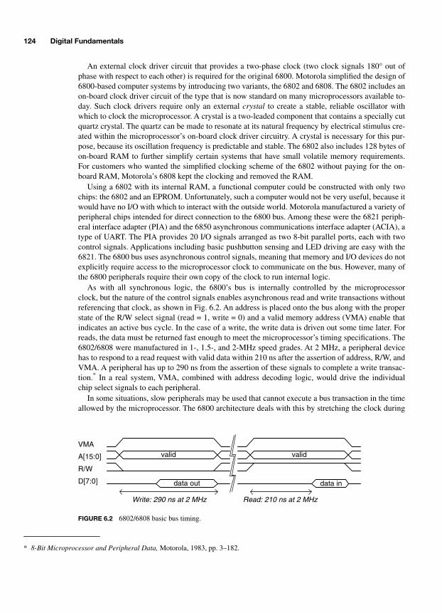
124 Digital Fundamentals
An external clock driver circuit that provides a two-phase clock (two clock signals 180° out ofphase with respect to each other) is required for the original 6800. Motorola simplified the design of6800-based computer systems by introducing two variants, the 6802 and 6808. The 6802 includes anon-board clock driver circuit of the type that is now standard on many microprocessors available to-day. Such clock drivers require only an external
crystal
to create a stable, reliable oscillator withwhich to clock the microprocessor. A crystal is a two-leaded component that contains a specially cutquartz crystal. The quartz can be made to resonate at its natural frequency by electrical stimulus cre-ated within the microprocessor’s on-board clock driver circuitry. A crystal is necessary for this pur-pose, because its oscillation frequency is predictable and stable. The 6802 also includes 128 bytes ofon-board RAM to further simplify certain systems that have small volatile memory requirements.For customers who wanted the simplified clocking scheme of the 6802 without paying for the on-board RAM, Motorola’s 6808 kept the clocking and removed the RAM.
Using a 6802 with its internal RAM, a functional computer could be constructed with only twochips: the 6802 and an EPROM. Unfortunately, such a computer would not be very useful, because itwould have no I/O with which to interact with the outside world. Motorola manufactured a variety ofperipheral chips intended for direct connection to the 6800 bus. Among these were the 6821 periph-eral interface adapter (PIA) and the 6850 asynchronous communications interface adapter (ACIA), atype of UART. The PIA provides 20 I/O signals arranged as two 8-bit parallel ports, each with twocontrol signals. Applications including basic pushbutton sensing and LED driving are easy with the6821. The 6800 bus uses asynchronous control signals, meaning that memory and I/O devices do notexplicitly require access to the microprocessor clock to communicate on the bus. However, many ofthe 6800 peripherals require their own copy of the clock to run internal logic.
As with all synchronous logic, the 6800’s bus is internally controlled by the microprocessorclock, but the nature of the control signals enables asynchronous read and write transactions withoutreferencing that clock, as shown in Fig. 6.2. An address is placed onto the bus along with the properstate of the R/W select signal (read = 1, write = 0) and a valid memory address (VMA) enable thatindicates an active bus cycle. In the case of a write, the write data is driven out some time later. Forreads, the data must be returned fast enough to meet the microprocessor’s timing specifications. The6802/6808 were manufactured in 1-, 1.5-, and 2-MHz speed grades. At 2 MHz, a peripheral devicehas to respond to a read request with valid data within 210 ns after the assertion of address, R/W, andVMA. A peripheral has up to 290 ns from the assertion of these signals to complete a write transac-tion.
*
In a real system, VMA, combined with address decoding logic, would drive the individualchip select signals to each peripheral.
In some situations, slow peripherals may be used that cannot execute a bus transaction in the timeallowed by the microprocessor. The 6800 architecture deals with this by stretching the clock during
*
8-Bit Microprocessor and Peripheral Data,
Motorola, 1983, pp. 3–182.
A[15:0]
VMA
D[7:0]
R/W
valid
data out
Write: 290 ns at 2 MHz
valid
data in
Read: 210 ns at 2 MHz
FIGURE 6.2 6802/6808 basic bus timing.
-Balch.book Page 124 Thursday, May 15, 2003 3:46 PM
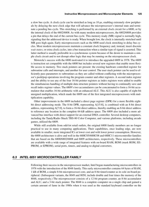
Instructive Microprocessors and Microcomputer Elements 125
a slow bus cycle. A clock cycle can be stretched as long as 10 µs, enabling extremely slow peripher-als by delaying the next clock edge that will advance the microprocessor’s internal state and termi-nate a pending bus cycle. This stretching is performed by an external clock circuit for a 6800, or bythe internal clock of the 6802/6808. As with many modern microprocessors, the 6802/6808 providesa pin that delays the end of the current bus cycle. This memory ready (MR) signal is normally high,signaling that the addressed device is ready. When brought low, the clock is internally stretched untilMR goes high again. Early microprocessors such as the 6800 used clock stretching to delay bus cy-cles. Most modern microprocessors maintain a constant clock frequency and, instead, insert discrete
wait states
, or extra clock cycles, into a bus transaction when a similar type of signal is asserted. Thislatter method is usually preferable in a synchronous system because of the desire to maintain a sim-ple clock circuit and to not disrupt other logic that may be running on the microprocessor clock.
Motorola’s success with the 6800 motivated it to introduce the upgraded 6809 in 1978. The 6809is instruction set compatible with the 6800 but includes several new registers that enable more flexi-ble access to memory. Two stack pointers are present: the existing hardware controlled register forsubroutine calls and interrupts, and another for user control. The user stack pointer can be used to ef-ficiently pass parameters to subroutines as they are called without conflicting with the microproces-sor’s push/pop operations involving the program counter and other registers. A second index registerand the ability to use any of the four 16-bit pointer registers as index registers were added to enablethe simultaneous handling of multiple data structure pointers without having to continually save andrecall index register values. The 6809’s two accumulators can be concatenated to form a 16-bit accu-mulator that enables 16-bit arithmetic with an enhanced ALU. This ALU is also capable of eight-bitunsigned multiplication, which made the 6809 one of the first integrated microprocessors with mul-tiplication capability.
Other improvements in the 6809 included a direct page register (DPR) for a more flexible eight-bit direct addressing mode. The 8-bit DPR, representing A[15:8], is combined with an 8-bit directaddress, representing A[7:0], to form a 16-bit direct address, thereby enabling an 8-bit direct addressto reference any location in the complete 64-kB address space. The 6809 also included a more ad-vanced bus interface with direct support for an external DMA controller. Several desktop computers,including the Tandy/Radio Shack TRS-80 Color Computer, and various platforms, including arcadegames, utilized the 6809.
While still available from odd-lot retail outlets, the original 6800 family members are no longerpractical to use in many computing applications. Their capabilities, once leading edge, are nowavailable in smaller, more integrated ICs at lower cost and with lower power consumption. However,the 6800 architecture is alive and well in the 68HC05/68HC08 and 68HC11 microcontroller familiesthat are based on the 6800/6802/6808 and 6809 architectures, respectively. These microcontrollersare available with a wide range of integrated features with on-board RAM, ROM (mask ROM, EE-PROM, or EPROM), serial ports, timers, and analog-to-digital converters.
6.3 INTEL 8051 MICROCONTROLLER FAMILY
Following their success in the microprocessor market, Intel began manufacturing microcontrollers in1976 with the introduction of the 8048 family. This early microcontroller contains 64 bytes of RAM,1 kB of ROM, a simple 8-bit microprocessor core, and an 8-bit timer/counter as its sole on-board pe-ripheral. (Subsequent variants, the 8049 and 8050, include double and four times the memory of the8048, respectively.) The microprocessor consists of a 12-bit program counter, an 8-bit accumulatorand ALU, and a 3-bit stack pointer. The 8048 is a complete computer on a single chip and gained acertain amount of fame in the 1980s when it was used as the standard keyboard controller on the
-Balch.book Page 125 Thursday, May 15, 2003 3:46 PM

126 Digital Fundamentals
IBM PC because of its simplicity and low cost. The 8048 was manufactured in a 40-pin DIP andcould be expanded with external memory and peripherals via an optional external address/data bus.However, when operated as a nonexpanded single-chip computer, the pins that would otherwisefunction as its bus were available for general I/O purposes—a practice that is fairly standard onmicrocontrollers.
Motivated by the popularity of the 8048, Intel introduced the 8051 microcontroller in 1980, whichis substantially more powerful and flexible. The 8051’s basic architecture is shown in Fig. 6.3. Itcontains 128 bytes of RAM, 4 kB of ROM, two 16-bit timer/counters, and a serial port. Registerswithin the microprocessor are 8 bits wide except for the 16-bit data pointer (DPTR) and programcounter (PC). Memory is divided into mutually exclusive program and data sections that each can beexpanded up to 64 kB in size via an external bus. Expansion is accomplished by borrowing pinsfrom two of the four 8-bit I/O ports. Intel manufactured several variants of the 8051. The 8052 dou-bled the amount of on-chip memory to 256 bytes of RAM and 8 kB of ROM and added a third timer.The 8031/8032 are 8051/8052 chips without on-board ROM. The 8751/8752 are 8051/8052 deviceswith EPROM instead of mask ROM. As time went by and the popularity of the 8051 family in-creased, other companies licensed the core architecture and developed many variants with differingmixes of memory and peripherals.
Ports 0 through 3 are each eight-bit bidirectional I/O structures that can be used as either general-purpose signals or as dedicated interface signals according to the system configuration. In a single-chip configuration where all memory is contained on board, the four ports may be assigned freely.Some peripheral functions use these I/O pins, but if a specific function is not required, the pins maybe used in a generic manner. Port 3 is the default peripheral port where pins are used for the serialport’s transmit and receive, external interrupt request inputs, counter increment inputs, and externalbus expansion control signals. Port 1 is a general-purpose port that is also assigned for additional pe-ripheral support signals when an 8051 variant contains additional peripheral functions beyond whatcan be supported on port 3 alone.
In a multichip configuration where memory and/or additional peripherals are added externally,ports 0 and 2 are used for bus expansion. Port 0 implements a multiplexed address/data bus wherethe 8051 first drives the lower eight address bits and then either drives write-data or samples read-data in a conventional bidirectional data bus scheme. In this standard configuration, the lower ad-dress bits, A[7:0], are latched externally by a discrete logic chip (generally a 74LS373 or similar),and the 8051 drives an address latch enable (ALE) signal to control this latch as shown in Fig. 6.4.This multiplexed address/data scheme saves precious pins on the microcontroller that can be used
SpecialFunctionRegisters
Peripherals:Timers,
Serial, etc.
AccumulatorB Register
Status Word
Data Pointer
Stack Pointer
ALU
RAMROM
Program Counter
Port 0 (Addr+Data)Port 2 (Address)
Ports 1 & 3General I/O
internal control/data bus
microprocessor section
Clock Driver
FIGURE 6.3 8051 overall architecture.
-Balch.book Page 126 Thursday, May 15, 2003 3:46 PM

Instructive Microprocessors and Microcomputer Elements 127
for valuable I/O functions. Some applications may suffice with just an eight-bit external address bus.For example, if the only expansion necessary were a special purpose I/O device, 256 bytes wouldprobably be more than enough to communicate with the device. However, some applications de-mand a fully functional 16-bit external address bus. In these situations, port 2 is used to drive the up-per address bits, A[15:8].
The 8051’s microprocessor is very capable for such an early microcontroller. It includes integermultiply and divide instructions that utilize eight-bit operands in the accumulator and B register, andit then places the result back into those registers. The stack, which grows upward in memory, is re-stricted to on-board RAM only (256 bytes at most), so only an eight-bit stack pointer is imple-mented. Aside from the general-purpose accumulator and B registers, the 8051 instruction set candirectly reference 8 byte-wide general-purpose registers, numbered R0 through R7, that are mappedas 4 banks in the lower 32 bytes of on-board RAM. The active register bank can be changed at anytime by modifying two bank-select bits in the status word. The map of on-board data memory isshown in Table 6.2. At reset, register bank 0 is selected, and the stack pointer is set to 0x07, meaningthat the stack will actually begin at location 0x08 when the first byte is eventually pushed. Above theregister banks is a 16-byte (128-bit) region of memory that is bit addressable. Microcontroller appli-cations often involve reading status information, checking certain bits to detect particular events, andthen triggering other events. Using single bits rather than whole bytes to store status informationsaves precious memory in a microcontroller. Therefore, the 8051’s bit manipulation instructions canmake efficient use of the chip’s resources from both instruction execution and memory usage per-spectives. The remainder of the lower 128-byte memory region contains 80 bytes of general-purposememory.
The upper 128 bytes of data memory are split into two sections: special-function registers andRAM. Special-function registers are present in all 8051 variants, but their definitions change ac-cording to the specific mix of peripherals in each variant. Some special-function registers are stan-dard across all 8051 variants. These registers are typically those that were implemented on theoriginal 8051/8052 devices and include the accumulator and B registers; the stack pointer; the datapointer; and serial port, timer, and I/O port control registers. Each time a manufacturer adds an on-board peripheral to the 8051, accompanying control registers are added into the special-functionmemory region.
On variants that incorporate 256 bytes of on-board RAM, the upper 128 bytes are also mappedinto a parallel region alongside the special-function registers. Access between RAM and special-function registers is controlled by the addressing mode used in a given instruction. Special-functionregisters are accessed with direct addressing only. Therefore, such an instruction must follow the op-code with an eight-bit address. The upper 128 bytes of RAM are accessed with indirect addressingonly. Therefore, such an instruction must reference one of the eight general-purpose registers (R0
8051
Latch(e.g. 74LS373)
Port 0
Port 2
ALE
AddressDecode
A[7:0]
A[15:8]
MemoryDevice
D[7:0]
A[N:0]
CS*
FIGURE 6.4 8051 system with external address latch.
-Balch.book Page 127 Thursday, May 15, 2003 3:46 PM
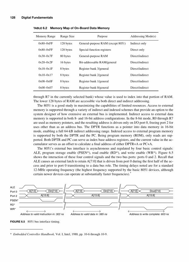
128 Digital Fundamentals
through R7 in the currently selected bank) whose value is used to index into that portion of RAM.The lower 128 bytes of RAM are accessible via both direct and indirect addressing.
The 8051 is a good study in maximizing the capabilities of limited resources. Access to externalmemory is supported through a variety of indirect and indexed schemes that provide an option to thesystem designer of how extensive an external bus is implemented. Indirect access to external datamemory is supported in both 8- and 16-bit address configurations. In the 8-bit mode, R0 through R7are used as memory pointers, and the resulting address is driven only on I/O port 0, freeing port 2 foruses other than as an address bus. The DPTR functions as a pointer into data memory in 16-bitmode, enabling a full 64-kB indirect addressing range. Indexed access to external program memoryis supported by both the DPTR and the PC. Being program memory (ROM), only reads are sup-ported. Both DPTR and PC can serve as index base address registers, and the current value in the ac-cumulator serves as an offset to calculate a final address of either DPTR+A or PC+A.
The 8051’s external bus interface is asynchronous and regulated by four basic control signals:ALE, program storage enable (PSEN*), read enable (RD*), and write enable (WR*). Figure 6.5shows the interaction of these four control signals and the two bus ports: ports 0 and 2. Recall thatALE causes an external latch to retain A[7:0] that is driven from port 0 during the first half of the ac-cess and prior to port 0 transitioning to a data bus role. The timing delays noted are for a standard12-MHz operating frequency (the highest frequency supported by the basic 8051 devices, althoughcertain newer devices can operate at substantially faster frequencies).
*
TABLE
6.2 Memory Map of On-Board Data Memory
Memory Range Range Size Purpose Addressing Mode(s)
0x80–0xFF 128 bytes General-purpose RAM (except 8051) Indirect only
0x80–0xFF 128 bytes Special-function registers Direct only
0x30–0x7F 80 bytes General-purpose RAM Direct/indirect
0x20–0x2F 16 bytes Bit-addressable RAM/general Direct/indirect
0x18–0x1F 8 bytes Register bank 3/general Direct/indirect
0x10–0x17 8 bytes Register bank 2/general Direct/indirect
0x08–0x0F 8 bytes Register bank 1/general Direct/indirect
0x00–0x07 8 bytes Register bank 0/general Direct/indirect
*
Embedded Controller Handbook,
Vol. I, Intel, 1988, pp. 10-6 through 10-9.
Port 0
ALE
RD*
PSEN*
A[7:0]
Address to valid instruction in: 302 ns
WR*
Port 2 A[15:8]
Din[7:0] A[7:0]
A[15:8]
Din[7:0] A[7:0]
A[15:8]
Dout[7:0]
Address to valid data in: 585 ns Address to write complete: 603 ns
FIGURE 6.5 8051 bus interface timing.
-Balch.book Page 128 Thursday, May 15, 2003 3:46 PM
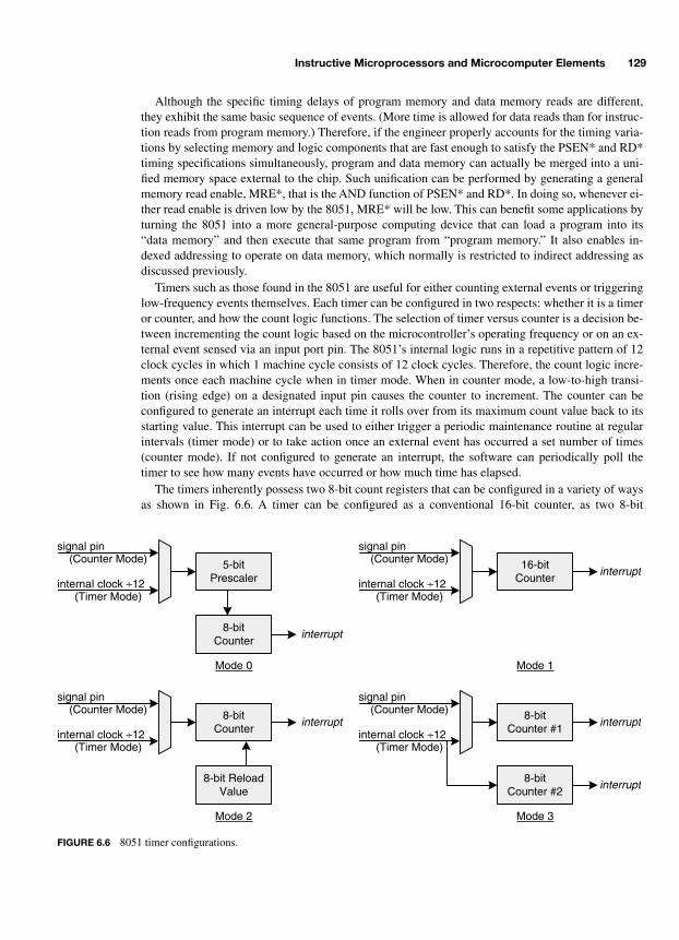
Instructive Microprocessors and Microcomputer Elements 129
Although the specific timing delays of program memory and data memory reads are different,they exhibit the same basic sequence of events. (More time is allowed for data reads than for instruc-tion reads from program memory.) Therefore, if the engineer properly accounts for the timing varia-tions by selecting memory and logic components that are fast enough to satisfy the PSEN* and RD*timing specifications simultaneously, program and data memory can actually be merged into a uni-fied memory space external to the chip. Such unification can be performed by generating a generalmemory read enable, MRE*, that is the AND function of PSEN* and RD*. In doing so, whenever ei-ther read enable is driven low by the 8051, MRE* will be low. This can benefit some applications byturning the 8051 into a more general-purpose computing device that can load a program into its“data memory” and then execute that same program from “program memory.” It also enables in-dexed addressing to operate on data memory, which normally is restricted to indirect addressing asdiscussed previously.
Timers such as those found in the 8051 are useful for either counting external events or triggeringlow-frequency events themselves. Each timer can be configured in two respects: whether it is a timeror counter, and how the count logic functions. The selection of timer versus counter is a decision be-tween incrementing the count logic based on the microcontroller’s operating frequency or on an ex-ternal event sensed via an input port pin. The 8051’s internal logic runs in a repetitive pattern of 12clock cycles in which 1 machine cycle consists of 12 clock cycles. Therefore, the count logic incre-ments once each machine cycle when in timer mode. When in counter mode, a low-to-high transi-tion (rising edge) on a designated input pin causes the counter to increment. The counter can beconfigured to generate an interrupt each time it rolls over from its maximum count value back to itsstarting value. This interrupt can be used to either trigger a periodic maintenance routine at regularintervals (timer mode) or to take action once an external event has occurred a set number of times(counter mode). If not configured to generate an interrupt, the software can periodically poll thetimer to see how many events have occurred or how much time has elapsed.
The timers inherently possess two 8-bit count registers that can be configured in a variety of waysas shown in Fig. 6.6. A timer can be configured as a conventional 16-bit counter, as two 8-bit
5-bitPrescaler
8-bitCounter
interrupt
Mode 0
signal pin
internal clock ÷12(Timer Mode)
(Counter Mode)
8-bitCounter
interrupt
Mode 2
8-bit ReloadValue
signal pin
internal clock ÷12(Timer Mode)
(Counter Mode) 8-bitCounter #1
interrupt
Mode 3
8-bitCounter #2
interrupt
signal pin
internal clock ÷12(Timer Mode)
(Counter Mode)
16-bitCounter
interrupt
Mode 1
signal pin
internal clock ÷12(Timer Mode)
(Counter Mode)
FIGURE 6.6 8051 timer configurations.
-Balch.book Page 129 Thursday, May 15, 2003 3:46 PM
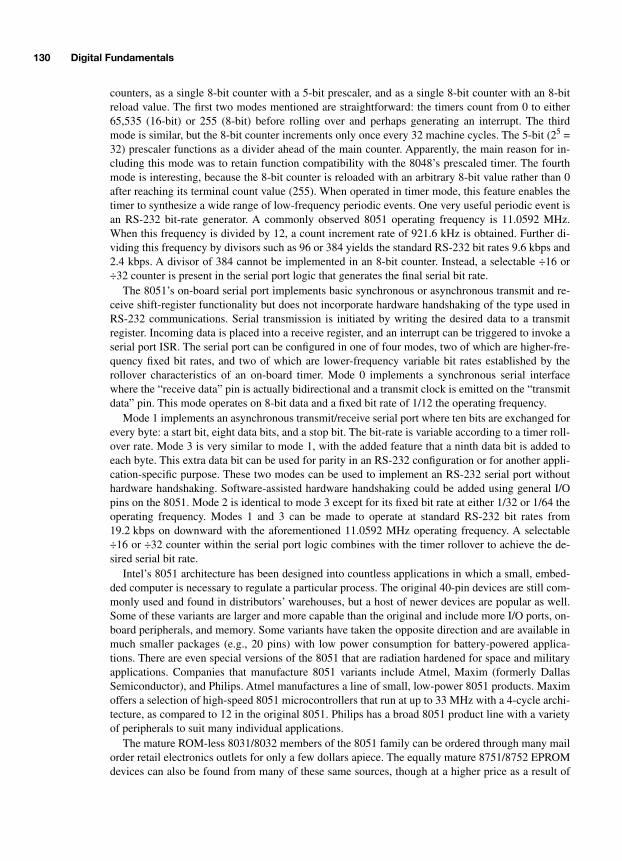
130 Digital Fundamentals
counters, as a single 8-bit counter with a 5-bit prescaler, and as a single 8-bit counter with an 8-bitreload value. The first two modes mentioned are straightforward: the timers count from 0 to either65,535 (16-bit) or 255 (8-bit) before rolling over and perhaps generating an interrupt. The thirdmode is similar, but the 8-bit counter increments only once every 32 machine cycles. The 5-bit (2
5
=32) prescaler functions as a divider ahead of the main counter. Apparently, the main reason for in-cluding this mode was to retain function compatibility with the 8048’s prescaled timer. The fourthmode is interesting, because the 8-bit counter is reloaded with an arbitrary 8-bit value rather than 0after reaching its terminal count value (255). When operated in timer mode, this feature enables thetimer to synthesize a wide range of low-frequency periodic events. One very useful periodic event isan RS-232 bit-rate generator. A commonly observed 8051 operating frequency is 11.0592 MHz.When this frequency is divided by 12, a count increment rate of 921.6 kHz is obtained. Further di-viding this frequency by divisors such as 96 or 384 yields the standard RS-232 bit rates 9.6 kbps and2.4 kbps. A divisor of 384 cannot be implemented in an 8-bit counter. Instead, a selectable ÷16 or÷32 counter is present in the serial port logic that generates the final serial bit rate.
The 8051’s on-board serial port implements basic synchronous or asynchronous transmit and re-ceive shift-register functionality but does not incorporate hardware handshaking of the type used inRS-232 communications. Serial transmission is initiated by writing the desired data to a transmitregister. Incoming data is placed into a receive register, and an interrupt can be triggered to invoke aserial port ISR. The serial port can be configured in one of four modes, two of which are higher-fre-quency fixed bit rates, and two of which are lower-frequency variable bit rates established by therollover characteristics of an on-board timer. Mode 0 implements a synchronous serial interfacewhere the “receive data” pin is actually bidirectional and a transmit clock is emitted on the “transmitdata” pin. This mode operates on 8-bit data and a fixed bit rate of 1/12 the operating frequency.
Mode 1 implements an asynchronous transmit/receive serial port where ten bits are exchanged forevery byte: a start bit, eight data bits, and a stop bit. The bit-rate is variable according to a timer roll-over rate. Mode 3 is very similar to mode 1, with the added feature that a ninth data bit is added toeach byte. This extra data bit can be used for parity in an RS-232 configuration or for another appli-cation-specific purpose. These two modes can be used to implement an RS-232 serial port withouthardware handshaking. Software-assisted hardware handshaking could be added using general I/Opins on the 8051. Mode 2 is identical to mode 3 except for its fixed bit rate at either 1/32 or 1/64 theoperating frequency. Modes 1 and 3 can be made to operate at standard RS-232 bit rates from19.2 kbps on downward with the aforementioned 11.0592 MHz operating frequency. A selectable÷16 or ÷32 counter within the serial port logic combines with the timer rollover to achieve the de-sired serial bit rate.
Intel’s 8051 architecture has been designed into countless applications in which a small, embed-ded computer is necessary to regulate a particular process. The original 40-pin devices are still com-monly used and found in distributors’ warehouses, but a host of newer devices are popular as well.Some of these variants are larger and more capable than the original and include more I/O ports, on-board peripherals, and memory. Some variants have taken the opposite direction and are available inmuch smaller packages (e.g., 20 pins) with low power consumption for battery-powered applica-tions. There are even special versions of the 8051 that are radiation hardened for space and militaryapplications. Companies that manufacture 8051 variants include Atmel, Maxim (formerly DallasSemiconductor), and Philips. Atmel manufactures a line of small, low-power 8051 products. Maximoffers a selection of high-speed 8051 microcontrollers that run at up to 33 MHz with a 4-cycle archi-tecture, as compared to 12 in the original 8051. Philips has a broad 8051 product line with a varietyof peripherals to suit many individual applications.
The mature ROM-less 8031/8032 members of the 8051 family can be ordered through many mailorder retail electronics outlets for only a few dollars apiece. The equally mature 8751/8752 EPROMdevices can also be found from many of these same sources, though at a higher price as a result of
-Balch.book Page 130 Thursday, May 15, 2003 3:46 PM

Instructive Microprocessors and Microcomputer Elements 131
the expense of the ceramic DIP in which they are most often found. More specialized 8051 variantsmay be available only through manufacturers’ authorized distributors.
6.4 MICROCHIP PIC
®
MICROCONTROLLER FAMILY
By the late 1980s, microcontrollers and certain microprocessors were well established in embeddedcontrol applications. Despite advances in technology, not many devices could simultaneously ad-dress the needs for low power, moderate processing throughput, very small packages, and diverse in-tegrated peripherals. Microchip Technology began offering a family of small peripheral interfacecontroller (PIC
®
)
*
devices in the early 1990s that addressed all four of these needs. Microchipdeveloped the compact PIC architecture based on a
reduced instruction set core
(RISC)microprocessor. The chips commonly run at up to 20 MHz and execute one instruction everymachine cycle (four clock cycles)—except branches that consume two cycles. The key conceptbehind the PIC family is simplicity. The original 16C5x family, shown in Fig. 6.7, implements a 33-instruction microprocessor core with a single working register (accumulator), W, and only a two-entry subroutine stack. These devices contain as little as 25 bytes of RAM and 512 bytes of ROM,and some are housed in an 18-pin package that can be smaller than a fingernail. The PIC devices arenot expandable via an external bus, further saving logic. This minimal architecture is what enablesrelatively high performance processing with low power consumption in a tiny package. Low-poweroperation is also coupled with a wide operating voltage range (2 to 6.25 V), further simplifyingcertain systems by not always requiring voltage regulation circuits.
No interrupt feature is included, which is a common criticism of the architecture; this was fixed insubsequent PIC microcontroller variants. PIC devices are, in general, fully static, meaning that theycan operate at an arbitrarily low frequency; 32 kHz is sometimes used in very power-sensitive appli-
* The Microchip name, PIC, and PICmicro are registered trademarks of Microchip Technology Inc. in the U.S.A. and othercountries.
Program Counter
2 Entry Stack
RAM
I/O Port ControlRegisters
Watchdog Timer
W
ALUStatus
Register
ROM
Clock Driver
Timer
Power-On Reset
FIGURE 6.7 PIC microcontroller 16C5x architecture.
-Balch.book Page 131 Thursday, May 15, 2003 3:46 PM

132 Digital Fundamentals
cations in which only microamps of current are consumed. To further reduce cost and complexity,the microcontrollers contain on-board clock drivers that work with a variety of external frequency-reference components. Quartz crystals are supported, as they are very accurate references. In verysmall systems wherein cost and size are absolutely paramount concerns, and absolute frequency ac-curacy is not a concern, less-expensive and smaller frequency references can be used with a PICmicrocontroller. One step down from a crystal is a
ceramic resonator,
which functions on a similarprinciple but with lower accuracy and cost. Finally, if the operating frequency can be allowed to varymore substantially with temperature, voltage, and time, a resistor/capacitor (RC) oscillator, thecheapest option, is supported. Tiny surface mount RC components take up very little circuit boardarea and cost pennies.
The original 16C5x family incorporates only the most basic of peripherals: power-on-reset, aneight-bit timer/counter, and a
watchdog timer
. A power-on reset circuit ensures that the microcon-troller reliably begins operation when power is applied by automatically controlling an internal resetsignal. On most microprocessors, reset is purely an external function. A
watchdog
timer can be con-figured to automatically reset the microcontroller if the system develops an unforeseen fault thatcauses the software to “crash.” The watchdog functions by continuously counting, and softwaremust periodically reset the counter to prevent it from reaching its terminal count value. If this valueis reached, the internal reset signal is asserted. Under normal circumstances where software is func-tioning properly, it resets the watchdog timer with plenty of time to spare. However, if the softwarecrashes, it will presumably not be able to reset the watchdog, and a system reset will soon follow.The watchdog timeout period is configurable from milliseconds to seconds. When using a watchdog,the timeout period is chosen to be long enough so that software can reliably reset the counter to pre-vent accidental reset, yet short enough to catch a fault and reset the system before serious problemsresult.
The PIC microcontroller’s RISC instruction set obeys the tenets of the general RISC style: ac-complish the same task with more simple instructions instead of fewer complex ones. Fewer types ofsimple instructions require less processing logic within the chip. As an example, there are just twobranch instructions:
CALL
and
GOTO
.
CALL
is an unconditional branch-to-subroutine that placesthe current PC onto the stack. It is the programmer’s responsibility to not nest subroutines more thantwo deep to avoid overflowing the stack.
GOTO
simply loads a new value into the PC. To implementconditional branches, these instructions are paired with one of four instructions that perform an ac-tion and then skip the following instruction if a particular result is true.
INCFSZ
and
DECFSZ
incre-ment or decrement a designated register, respectively, and then skip the following instruction if theresult is zero.
BTFSC
and
BTFSS
test a specified bit in a register and then skip the following in-struction if the bit is 0 or 1, respectively. Using the first pair of instructions, a loop could be writtenas shown in Fig. 6.8.
Assembly languages commonly offer the programmer a means of representing numeric valueswith alphanumeric labels for convenience. Here, the loop variable
COUNT
is set to address 0 with an
equate
directive that is recognized and processed by the assembler.
MOVWF
transfers the value in the
COUNT EQU 0 ; define COUNT at address 0
MOVLW 0x09 ; 9 loop iterations MOVW F COUNT ; iteration tracking register
LOOP_START <loop instructions> ; body of loop DECFSZ COUNT,1 ; done with loop yet?
GOTO LOOP_START ; non-zero, keep going... <more instructions> ; zero, loop is done...
FIGURE 6.8 16C5x assembly language loop.
-Balch.book Page 132 Thursday, May 15, 2003 3:46 PM
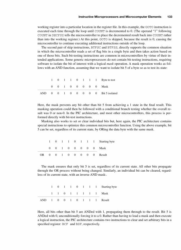
Instructive Microprocessors and Microcomputer Elements 133
working register into a particular location in the register file. In this example, the
GOTO
instruction isexecuted each time through the loop until
COUNT
is decremented to 0. (The operand “1” following
COUNT
in
DECFSZ
tells the microcontroller to place the decremented result back into
COUNT
ratherthan into the working register.) At this point,
GOTO
is skipped, because the result is 0, causing themicrocontroller to continue executing additional instructions outside of the loop.
The second pair of skip instructions,
BTFSC
and
BTFSS
, directly supports the common situationin which the microcontroller reads a set of flag bits in a single byte and then takes action based onone of those bits. Such bit-testing instructions are common in microcontrollers by virtue of their in-tended applications. Some generic microprocessors do not contain bit-testing instructions, requiringsoftware to isolate the bit of interest with a logical
mask
operation. A mask operation works as fol-lows with an AND function, assuming that we want to isolate bit 5 of a byte so as to test its state:
Here, the mask prevents any bit other than bit 5 from achieving a 1 state in the final result. Thismasking operation could then be followed with a conditional branch testing whether the overall re-sult was 0 or non-0. In the PIC architecture, and most other microcontrollers, this process is per-formed directly with bit-test instructions.
Masking also works to set or clear individual bits but, here again, the PIC architecture containsspecial instructions to optimize this common microcontroller function. Using the above example, bit5 can be set, regardless of its current state, by ORing the data byte with the same mask.
The mask ensures that only bit 5 is set, regardless of its current state. All other bits propagatethrough the OR process without being changed. Similarly, an individual bit can be cleared, regard-less of its current state, with an inverse AND mask:.
Here, all bits other than bit 5 are ANDed with 1, propagating them through to the result. Bit 5 isANDed with 0, unconditionally forcing it to a 0. Rather than having to load a mask and then executea logical instruction, the PIC architecture contains two instructions to clear and set arbitrary bits in aspecified register:
BCF
and
BSF
, respectively.
1 0 1 1 0 1 1 1 Byte to test
0 0 1 0 0 0 0 0 Mask
AND 0 0 1 0 0 0 0 0 Bit 5 isolated
1 0 1 1 0 1 1 1 Starting byte
0 0 1 0 0 0 0 0 Mask
OR 0 0 1 0 0 0 0 0 Result
1 0 1 1 0 1 1 1 Starting byte
1 1 0 1 1 1 1 1 Mask
AND 1 0 0 1 0 1 1 1 Result
-Balch.book Page 133 Thursday, May 15, 2003 3:46 PM
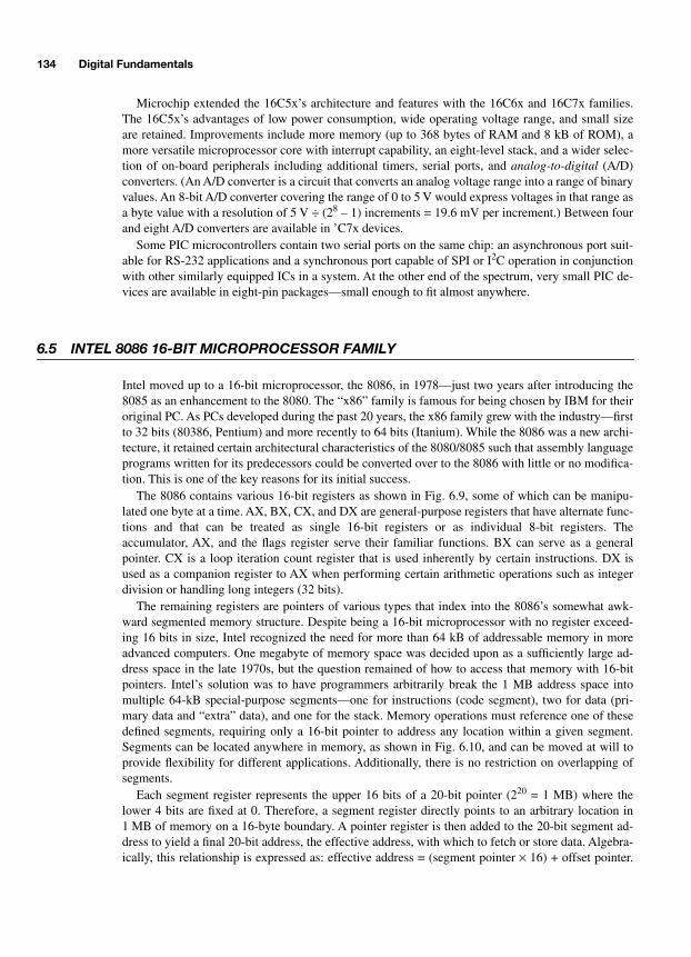
134 Digital Fundamentals
Microchip extended the 16C5x’s architecture and features with the 16C6x and 16C7x families.The 16C5x’s advantages of low power consumption, wide operating voltage range, and small sizeare retained. Improvements include more memory (up to 368 bytes of RAM and 8 kB of ROM), amore versatile microprocessor core with interrupt capability, an eight-level stack, and a wider selec-tion of on-board peripherals including additional timers, serial ports, and
analog-to-digital
(A/D)converters. (An A/D converter is a circuit that converts an analog voltage range into a range of binaryvalues. An 8-bit A/D converter covering the range of 0 to 5 V would express voltages in that range asa byte value with a resolution of 5 V ÷ (2
8
– 1) increments = 19.6 mV per increment.) Between fourand eight A/D converters are available in ’C7x devices.
Some PIC microcontrollers contain two serial ports on the same chip: an asynchronous port suit-able for RS-232 applications and a synchronous port capable of SPI or I
2
C operation in conjunctionwith other similarly equipped ICs in a system. At the other end of the spectrum, very small PIC de-vices are available in eight-pin packages—small enough to fit almost anywhere.
6.5 INTEL 8086 16-BIT MICROPROCESSOR FAMILY
Intel moved up to a 16-bit microprocessor, the 8086, in 1978—just two years after introducing the8085 as an enhancement to the 8080. The “x86” family is famous for being chosen by IBM for theiroriginal PC. As PCs developed during the past 20 years, the x86 family grew with the industry—firstto 32 bits (80386, Pentium) and more recently to 64 bits (Itanium). While the 8086 was a new archi-tecture, it retained certain architectural characteristics of the 8080/8085 such that assembly languageprograms written for its predecessors could be converted over to the 8086 with little or no modifica-tion. This is one of the key reasons for its initial success.
The 8086 contains various 16-bit registers as shown in Fig. 6.9, some of which can be manipu-lated one byte at a time. AX, BX, CX, and DX are general-purpose registers that have alternate func-tions and that can be treated as single 16-bit registers or as individual 8-bit registers. Theaccumulator, AX, and the flags register serve their familiar functions. BX can serve as a generalpointer. CX is a loop iteration count register that is used inherently by certain instructions. DX isused as a companion register to AX when performing certain arithmetic operations such as integerdivision or handling long integers (32 bits).
The remaining registers are pointers of various types that index into the 8086’s somewhat awk-ward segmented memory structure. Despite being a 16-bit microprocessor with no register exceed-ing 16 bits in size, Intel recognized the need for more than 64 kB of addressable memory in moreadvanced computers. One megabyte of memory space was decided upon as a sufficiently large ad-dress space in the late 1970s, but the question remained of how to access that memory with 16-bitpointers. Intel’s solution was to have programmers arbitrarily break the 1 MB address space intomultiple 64-kB special-purpose segments—one for instructions (code segment), two for data (pri-mary data and “extra” data), and one for the stack. Memory operations must reference one of thesedefined segments, requiring only a 16-bit pointer to address any location within a given segment.Segments can be located anywhere in memory, as shown in Fig. 6.10, and can be moved at will toprovide flexibility for different applications. Additionally, there is no restriction on overlapping ofsegments.
Each segment register represents the upper 16 bits of a 20-bit pointer (2
20
= 1 MB) where thelower 4 bits are fixed at 0. Therefore, a segment register directly points to an arbitrary location in1 MB of memory on a 16-byte boundary. A pointer register is then added to the 20-bit segment ad-dress to yield a final 20-bit address, the effective address, with which to fetch or store data. Algebra-ically, this relationship is expressed as: effective address = (segment pointer
×
16) + offset pointer.
-Balch.book Page 134 Thursday, May 15, 2003 3:46 PM
Instructive Microprocessors and Microcomputer Elements 135
AH ALAX Accumulator
BH BLBX Base
CH CLCX Count
DH DLDX Data
8 bits
16 bits
8 bits
SP Stack pointer
BP Base pointer
SI Source index
DI Destination index
IP Instruction pointer
Flags ALU status flags
CS Code segment
DS Data segment
SS Stack segment
ES Extra data segment
FIGURE 6.9 8086 register set.
CS
DS
SS
ES
inaccessiblememory outside
of currentlydefined segments
Data segment
Stack segment
Code segment
Extra data segment
overlap
Memory bottom: 0x00000
Memory top: 0xFFFFF
FIGURE 6.10 8086 segments.
-Balch.book Page 135 Thursday, May 15, 2003 3:46 PM
136 Digital Fundamentals
Inside the microprocessor, this math is performed by shifting the segment pointer (0x135F) left byfour bits and then adding the offset pointer (0x0102) as shown below.
This segmented addressing scheme has some awkward characteristics. First, programs must orga-nize their instructions and data into 64-kB chunks and properly keep track of which portions are be-ing accessed. If data outside of the current segments is desired, the appropriate segment registermust be updated. Second, the same memory location can be represented by multiple combinations ofsegment and offset values, which can cause confusion in sorting out which instruction is accessingwhich location in memory. Nonetheless, programmers and the manufacturers of their developmenttools have figured out ways to avoid these traps and others like them.
Instructions that reference memory implicitly or explicitly determine which offset pointer isadded to which segment register to yield the desired effective address. For example, a push or popinstruction inherently uses the stack pointer in combination with the stack segment register. How-ever, an instruction to move data from memory to the accumulator can use one of multiple pointerregisters relative to any of the segment registers.
The 8086’s reset and interrupt vectors are located at opposite ends of the memory space. On reset,the instruction pointer is set to 0xFFFF0, and the microprocessor begins executing instructions fromthis address. Therefore, rather than being a true vector, the 16-byte reset region contains normal exe-cutable instructions. The interrupt vectors are located at the bottom of the memory space startingfrom address 0, and there are 256 vectors, one for each of the 256 interrupt types. Each interrupt vec-tor is composed of a 2-byte segment address and a 2-byte offset address, from which a 20-bit effec-tive address is calculated. When the 8086’s INTR pin is driven high, an interrupt acknowledgeprocess begins via the INTA* output pin. The 8086 pulses INTA* low twice and, on the secondpulse, the interrupting peripheral drives an interrupt type, or vector number, onto the eight lower bitsof the data bus. The vector number is used to index into the interrupt vector table by multiplying itby 4 (shifting left by two bits), because each vector consists of four bytes. For example, interrupttype 0x03 would cause the microprocessor to fetch four bytes from addresses 0x0C through 0x0F.Interrupts triggered by the INTR pin are all maskable via an internal control bit. Software can alsotrigger interrupts of various types via the
INT
instruction. A nonmaskable interrupt can be triggeredby external hardware via the NMI pin. NMI initiates the type-2 interrupt service routine at the ad-dress indicated by the vector at 0x08-0x0B.
Locating the reset boot code at the top of memory and the interrupt vectors at the bottom oftenleads to an 8086 computer architecture with ROM at the top and some RAM at the bottom. ROMmust be at the top, for obvious reasons. Placing the interrupt vector table in RAM enables a flexiblesystem in which software applications can install their own ISRs to perform various tasks. On theoriginal IBM PC platform, it was not uncommon for programs to insert their own ISR addresses intocertain interrupt vectors located in RAM. The system timer and keyboard interrupts were commonobjects of this activity. Because the PC’s operating system already implemented ISRs for these inter-rupts, the program could redirect the interrupt vector to its own ISR and then call the system’s de-fault ISR when its own ISR completed execution. If properly done, this interrupt chaining processcould add new features to a PC without harming the existing housekeeping chores performed by thestandard ISRs. Chaining the keyboard interrupt could enable a program that is normally dormant topop up each time a particular key sequence is pressed.
1 3 5 F 0 Segment pointer
+ 0 1 0 2 Offset pointer
1 3 6 F 2 Effective address
-Balch.book Page 136 Thursday, May 15, 2003 3:46 PM
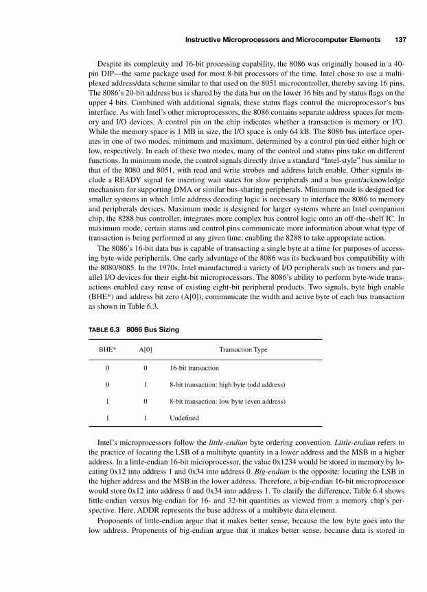
Instructive Microprocessors and Microcomputer Elements 137
Despite its complexity and 16-bit processing capability, the 8086 was originally housed in a 40-pin DIP—the same package used for most 8-bit processors of the time. Intel chose to use a multi-plexed address/data scheme similar to that used on the 8051 microcontroller, thereby saving 16 pins.The 8086’s 20-bit address bus is shared by the data bus on the lower 16 bits and by status flags on theupper 4 bits. Combined with additional signals, these status flags control the microprocessor’s businterface. As with Intel’s other microprocessors, the 8086 contains separate address spaces for mem-ory and I/O devices. A control pin on the chip indicates whether a transaction is memory or I/O.While the memory space is 1 MB in size, the I/O space is only 64 kB. The 8086 bus interface oper-ates in one of two modes, minimum and maximum, determined by a control pin tied either high orlow, respectively. In each of these two modes, many of the control and status pins take on differentfunctions. In minimum mode, the control signals directly drive a standard “Intel-style” bus similar tothat of the 8080 and 8051, with read and write strobes and address latch enable. Other signals in-clude a READY signal for inserting wait states for slow peripherals and a bus grant/acknowledgemechanism for supporting DMA or similar bus-sharing peripherals. Minimum mode is designed forsmaller systems in which little address decoding logic is necessary to interface the 8086 to memoryand peripherals devices. Maximum mode is designed for larger systems where an Intel companionchip, the 8288 bus controller, integrates more complex bus control logic onto an off-the-shelf IC. Inmaximum mode, certain status and control pins communicate more information about what type oftransaction is being performed at any given time, enabling the 8288 to take appropriate action.
The 8086’s 16-bit data bus is capable of transacting a single byte at a time for purposes of access-ing byte-wide peripherals. One early advantage of the 8086 was its backward bus compatibility withthe 8080/8085. In the 1970s, Intel manufactured a variety of I/O peripherals such as timers and par-allel I/O devices for their eight-bit microprocessors. The 8086’s ability to perform byte-wide trans-actions enabled easy reuse of existing eight-bit peripheral products. Two signals, byte high enable(BHE*) and address bit zero (A[0]), communicate the width and active byte of each bus transactionas shown in Table 6.3.
Intel’s microprocessors follow the
little-endian
byte ordering convention.
Little-endian
refers tothe practice of locating the LSB of a multibyte quantity in a lower address and the MSB in a higheraddress. In a little-endian 16-bit microprocessor, the value 0x1234 would be stored in memory by lo-cating 0x12 into address 1 and 0x34 into address 0.
Big-endian
is the opposite: locating the LSB inthe higher address and the MSB in the lower address. Therefore, a big-endian 16-bit microprocessorwould store 0x12 into address 0 and 0x34 into address 1. To clarify the difference, Table 6.4 showslittle-endian versus big-endian for 16- and 32-bit quantities as viewed from a memory chip’s per-spective. Here, ADDR represents the base address of a multibyte data element.
Proponents of little-endian argue that it makes better sense, because the low byte goes into thelow address. Proponents of big-endian argue that it makes better sense, because data is stored in
TABLE
6.3 8086 Bus Sizing
BHE* A[0] Transaction Type
0 0 16-bit transaction
0 1 8-bit transaction: high byte (odd address)
1 0 8-bit transaction: low byte (even address)
1 1 Undefined
-Balch.book Page 137 Thursday, May 15, 2003 3:46 PM
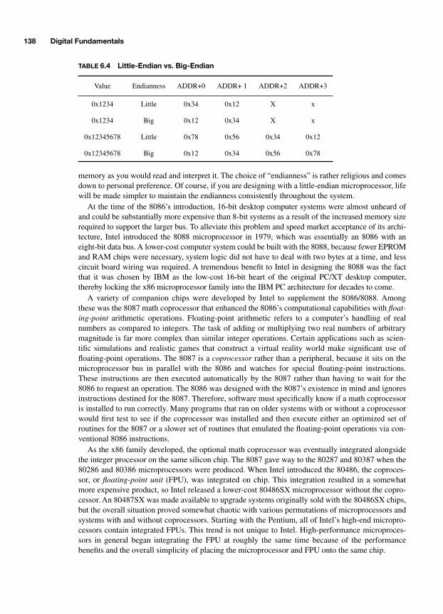
138 Digital Fundamentals
memory as you would read and interpret it. The choice of “endianness” is rather religious and comesdown to personal preference. Of course, if you are designing with a little-endian microprocessor, lifewill be made simpler to maintain the endianness consistently throughout the system.
At the time of the 8086’s introduction, 16-bit desktop computer systems were almost unheard ofand could be substantially more expensive than 8-bit systems as a result of the increased memory sizerequired to support the larger bus. To alleviate this problem and speed market acceptance of its archi-tecture, Intel introduced the 8088 microprocessor in 1979, which was essentially an 8086 with aneight-bit data bus. A lower-cost computer system could be built with the 8088, because fewer EPROMand RAM chips were necessary, system logic did not have to deal with two bytes at a time, and lesscircuit board wiring was required. A tremendous benefit to Intel in designing the 8088 was the factthat it was chosen by IBM as the low-cost 16-bit heart of the original PC/XT desktop computer,thereby locking the x86 microprocessor family into the IBM PC architecture for decades to come.
A variety of companion chips were developed by Intel to supplement the 8086/8088. Amongthese was the 8087 math coprocessor that enhanced the 8086’s computational capabilities with
float-ing-point
arithmetic operations. Floating-point arithmetic refers to a computer’s handling of realnumbers as compared to integers. The task of adding or multiplying two real numbers of arbitrarymagnitude is far more complex than similar integer operations. Certain applications such as scien-tific simulations and realistic games that construct a virtual reality world make significant use offloating-point operations. The 8087 is a
coprocessor
rather than a peripheral, because it sits on themicroprocessor bus in parallel with the 8086 and watches for special floating-point instructions.These instructions are then executed automatically by the 8087 rather than having to wait for the8086 to request an operation. The 8086 was designed with the 8087’s existence in mind and ignoresinstructions destined for the 8087. Therefore, software must specifically know if a math coprocessoris installed to run correctly. Many programs that ran on older systems with or without a coprocessorwould first test to see if the coprocessor was installed and then execute either an optimized set ofroutines for the 8087 or a slower set of routines that emulated the floating-point operations via con-ventional 8086 instructions.
As the x86 family developed, the optional math coprocessor was eventually integrated alongsidethe integer processor on the same silicon chip. The 8087 gave way to the 80287 and 80387 when the80286 and 80386 microprocessors were produced. When Intel introduced the 80486, the coproces-sor, or
floating-point unit
(FPU), was integrated on chip. This integration resulted in a somewhatmore expensive product, so Intel released a lower-cost 80486SX microprocessor without the copro-cessor. An 80487SX was made available to upgrade systems originally sold with the 80486SX chips,but the overall situation proved somewhat chaotic with various permutations of microprocessors andsystems with and without coprocessors. Starting with the Pentium, all of Intel’s high-end micropro-cessors contain integrated FPUs. This trend is not unique to Intel. High-performance microproces-sors in general began integrating the FPU at roughly the same time because of the performancebenefits and the overall simplicity of placing the microprocessor and FPU onto the same chip.
TABLE 6.4 Little-Endian vs. Big-Endian
Value Endianness ADDR+0 ADDR+ 1 ADDR+2 ADDR+3
0x1234 Little 0x34 0x12 X x
0x1234 Big 0x12 0x34 X x
0x12345678 Little 0x78 0x56 0x34 0x12
0x12345678 Big 0x12 0x34 0x56 0x78
-Balch.book Page 138 Thursday, May 15, 2003 3:46 PM
Instructive Microprocessors and Microcomputer Elements 139
6.6 MOTOROLA 68000 16/32-BIT MICROPROCESSOR FAMILY
Motorola followed its 6800 family by leaping directly to a hybrid 16/32-bit microprocessor architec-ture. Introduced in 1979, the 68000 is a 16-bit microprocessor, due to its 16-bit ALU, but it containsall 32-bit registers and a linear, nonsegmented 32-bit address space. (The original 68000 did notbring out all 32 address bits as signal pins but, more importantly, there are no architectural limita-tions of using all 32 bits.) That the register and memory architecture is inherently 32 bits made the68000 family easily scalable to a full 32-bit internal architecture. Motorola upgraded the 68000 fam-ily with true 32-bit devices, including the 68020, 68040, and 68060, until switching to the PowerPCarchitecture in the latter portion of the 1990s for new high-performance computing applications. Ap-ple Computer used the 68000 family in their popular line of Macintosh desktop computers. Today,the 68000 family lives on primarily as a mid-level embedded-processor core product. Motorola man-ufacturers a variety of high-end microcontrollers that use 32-bit 68000 microprocessor cores. How-ever, in recent years Motorola has begun migrating these products, as well as their general-purposemicroprocessors, to the PowerPC architecture, reducing the number of new designs that use the68000 family.
The 68000 inherently supports modern software operating systems (OSs) by recognizing twomodes of operation: supervisor mode and user mode. A modern OS does not grant unlimited accessto application software in using the computer’s resources. Rather, the OS establishes a restricted op-erating environment into which a program is loaded. Depending on the specific OS, applicationsmay not be able to access certain areas of memory or I/O devices that have been declared off limitsby the OS. This can prevent a fault in one program from crashing the entire computer system. TheOS kernel, the core low-level software that keeps the computer running properly, has special privi-leges that allow it unrestricted access to the computer for the purposes of establishing all of the rulesand boundaries under which programs run. Hardware support for multiple privilege levels is crucialfor such a scheme to prevent unauthorized programs from freely accessing restricted resources. Asmicroprocessors developed over the last few decades, more hardware support for OS privileges wasadded. That the 68000 included such concepts in 1979 is a testimony to its scalable architecture.
Sixteen 32-bit general-purpose registers, one of which is a user stack pointer (USP), and an 8-bitcondition code register are accessible from user mode as shown in Fig. 6.11. Additionally, a supervi-sor stack pointer (SSP) and eight additional status bits are accessible from supervisor mode. Com-puter systems do not have to implement the two modes of operation if the application does notrequire it. In such cases, the 68000 can be run permanently in supervisor mode to enable full accessto all resources by all programs. The SSP is used for stack operations while in supervisor mode, andthe USP is used for stack operations in user mode. User mode programs cannot change the USP, pre-venting them from relocating their stacks. Most modern operating systems are multitasking, mean-ing that they run multiple programs simultaneously. In reality, a microprocessor can only run oneprogram at a time. A multitasking OS uses a timer to periodically interrupt the microprocessor, per-haps 20 to 100 times per second, and place it into supervisor mode. Each time supervisor mode is in-voked, the kernel performs various maintenance tasks and swaps the currently running program withthe next program in the list of running programs. This swap, or context switch, can entail substantialmodifications to the microprocessor’s state when it returns from the kernel timer interrupt. In thecase of an original 68000 microprocessor, the kernel could change the return value of the PC, USP,the 16 general-purpose registers, and the status register. When normal execution resumes, the micro-processor is now executing a different program in exactly the same state at which it was previouslyinterrupted, because all of its registers are in the same state in which they were left. In such ascenario, each program has its own private stack, pointed to by a kernel-designated stack pointer.
The eight data registers, D0–D7, can be used for arbitrary ALU operations. The eight address reg-isters, A0–A7, can all be used as base addresses for indirect addressing and for certain 16- and 32-bit
-Balch.book Page 139 Thursday, May 15, 2003 3:46 PM
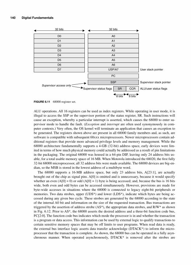
140 Digital Fundamentals
ALU operations. All 16 registers can be used as index registers. While operating in user mode, it isillegal to access the SSP or the supervisor portion of the status register, SR. Such instructions willcause an exception, whereby a particular interrupt is asserted, which causes the 68000 to enter su-pervisor mode to handle the fault. (Exception and interrupt are often used synonymously in com-puter contexts.) Very often, the OS kernel will terminate an application that causes an exception tobe generated. The registers shown above are present in all 68000 family members and, as such, aresoftware is compatible with subsequent 68xxx microprocessors. Newer microprocessors contain ad-ditional registers that provide more advanced privilege levels and memory management. While the68000 architecture fundamentally supports a 4-GB (32-bit) address space, early devices were lim-ited in terms of how much physical memory could actually be addressed as a result of pin limitationsin the packaging. The original 68000 was housed in a 64-pin DIP, leaving only 24 address bits us-able, for a total usable memory space of 16 MB. When Motorola introduced the 68020, the first fully32-bit 68000 microprocessor, all 32 address bits were made available. The 68000 devices are big-en-dian, so the MSB is stored in the lowest address of a multibyte word.
The 68000 supports a 16-MB address space, but only 23 address bits, A[23:1], are actuallybrought out of the chip as signal pins. A[0] is omitted and is unnecessary, because it would specifywhether an even (A[0] = 0) or odd (A[0] = 1) byte is being accessed; and, because the bus is 16 bitswide, both even and odd bytes can be accessed simultaneously. However, provisions are made forbyte-wide accesses in situations where the 68000 is connected to legacy eight-bit peripherals ormemories. Two data strobes, upper (UDS*) and lower (LDS*), indicate which bytes are being ac-cessed during any given bus cycle. These strobes are generated by the 68000 according to the stateof the internal A0 bit and information on the size of the requested transaction. Bus transactions aretriggered by the assertion of address strobe (AS*), the appropriate data strobes, and R/W* as shownin Fig. 6.12. Prior to AS*, the 68000 asserts the desired address and a three-bit function code bus,FC[2:0]. The function code bus indicates which mode the processor is in and whether the transactionis a program or data access. This information can be used by external logic to qualify transactions tocertain sensitive memory spaces that may be off limits to user programs. When read data is ready,the external bus interface logic asserts data transfer acknowledge (DTACK*) to inform the micro-processor that the transaction is complete. As shown, the 68000 bus can be operated in a fully asyn-chronous manner. When operated asynchronously, DTACK* is removed after the strobes are
32 bits
8 bits
USP/A7 User stack pointer
CCR ALU/user status flags
SSP Supervisor stack pointer
A6
A5
A4
A3
A2
A1
A0
32 bits
D7
D6
D5
D4
D3
D2
D1
D0
PC
SR
8 bits
Supervisor status flagsSupervisor access only
FIGURE 6.11 68000 register set.
-Balch.book Page 140 Thursday, May 15, 2003 3:46 PM

Instructive Microprocessors and Microcomputer Elements 141
removed, ensuring that the 68000 detected the assertion of DTACK*. If DTACK* is removed priorto the strobes, there is a chance of marginal timing where the 68000 may not properly detect the ac-knowledge, and it may wait forever for an acknowledge that has now passed. Writes are very similarto reads, with the obvious difference that R/W* is brought low, and data is driven by the 68000. An-other difference is that the data strobe assertion lags that of AS*.
Advanced microprocessors such as the 68000 are designed to recognize fault conditions whereinthe requested bus transaction cannot be completed. A bus fault can be caused by a variety of problems,including unauthorized access (e.g., user mode tries to write to a protected supervisor data space) oran access to a section of memory that is not filled by a memory or peripheral device. Software shouldnever access areas of memory that are off limits, because the results are unpredictable. Therefore,rather than simply issuing a false DTACK* and continuing with normal operation, the 68000 containsa bus error signal (BERR*) that behaves like DTACK* but triggers an exception rather than continu-ing normal execution. It is the responsibility of external logic to manage the DTACK* and BERR*signals according to the specific configuration and requirements of the particular system.
Operating the 68000 bus in an asynchronous manner is easy, but it reduces its bandwidth, becausedelays must be built into the acknowledge process to guarantee that both the 68000 and the interfacelogic maintain synchronization. Figure 6.12 shows read data being asserted prior to DTACK* and anarbitrary delay between the release of AS* and that of DTACK*. The data delay is necessary to guar-antee that the 68000 will see valid data when it detects a valid acknowledge. The second delay isnecessary to ensure that the 68000 completes the transaction, as noted previously. These delays canbe eliminated if the bus is operated synchronously by distributing the microprocessor clock to the in-terface logic and guaranteeing that various setup and hold timing requirements are met as specifiedby Motorola. In such a configuration, it is known from Motorola’s data sheet that the 68000 looksfor DTACK* each clock cycle, starting at a fixed time after asserting the strobes, and then samplesthe read-data one cycle after detecting DTACK* being active. Because synchronous timing rules areobeyed, it is guaranteed that the 68000 properly detects DTACK* and, therefore, DTACK* can beremoved without having to wait for the removal of the strobes. 68000 synchronous bus timing isshown in Fig. 6.13, where each transaction lasts a minimum of four clock cycles. A four-cycle trans-action is a zero wait state access. Wait states can be added by simply delaying the assertion ofDTACK* to the next cycle. However, to maintain proper timing, DTACK* (and BERR* and read-data) must always obey proper setup and hold requirements. As shown in the timing diagram, eachsignal transition, or edge, is time-bounded relative to a clock edge.
Read timing allows a single clock cycle between data strobe assertion and the return of DTACK*for a zero wait-state transaction. However, zero wait-state writes require DTACK* assertion at
A[23:1]
FC[2:0]
D[15:8]
AS*
valid
data in
valid
UDS*
LDS*
R/W*
D[7:0] data in
DTACK*16-bit read
valid
data in
valid
8-bit read (even byte, A0=0)
valid
data out
valid
8-bit write (odd byte, A0=1)
FIGURE 6.12 68000 asynchronous bus timing.
-Balch.book Page 141 Thursday, May 15, 2003 3:46 PM

142 Digital Fundamentals
roughly the same time as the data strobes. Therefore, the bus interface logic must make its decisionon asserting DTACK* based on the requested address when AS* is asserted. If the requested deviceis operational, DTACK* can be immediately asserted for a fast transaction. Unlike reads, where themicroprocessor must wait for a device to return data, writes can be acknowledged before they are ac-tually transferred to the device. In such a scheme, writes are posted within the bus interface logic.One or two cycles later, when the device accepts the posted write data, the bus interface logic finallycompletes the transaction without having delayed the microprocessor. If completion of the posted-write transaction takes longer than a few cycles, it could force a subsequent access to the same de-vice to incur wait states. Either a read or a write would be blocked until the original write was able tocomplete, thus freeing the device to handle the next transaction.
In addition to the basic bus interface, the 68000 supports bus arbitration to enable DMA or otherlogic to use the microprocessor bus for arbitrary applications. A bus request (BR*) signal is assertedby a device that wants to temporarily gain control of the bus. On the next clock cycle, when the mi-croprocessor is not inhibited by other operations, it asserts a bus grant (BG*) signal and places itsaddress, data, and control signals into tri-state so that they may be driven by the other device. The re-questing device then asserts bus grant acknowledge (BGACK*) to signal that it is controlling thebus, and it is then free to assert its own strobes, address, and data signals.
A variety of interrupts and exceptions are supported by the 68000. Some are triggered as a resultof instruction execution and some by external signals (e.g., BERR* or an interrupt request). Exam-ples of instruction exceptions are illegal user mode register accesses or a divide-by-zero error. Mostmicroprocessors that provide division capability contain some type of divide-by-zero error handling,because the result of such an operation is mathematically undefined and is usually the result of afault in the program. The 68000 contains an exception vector table that is 1,024 bytes long and re-sides at the beginning of memory at address 0. In a multitasking system, the bus interface logic mayrestrict access to the vector table to supervisor mode only. In such a case, a bus error could be trig-gered if a user mode program, indicated by FC[2:0], tried to write the table. Each of the 256 vectorentries is four bytes long and provides the starting address of the associated ISR. The one deviationfrom this rule is the reset vector, which actually consists of two entries at word addresses 0 and 4.Upon reset, the 68000 fetches an initial PC value from address 4 and an initial SSP value from ad-dress 0. Vectors 0 through 63 are assigned or reserved by Motorola for various hardware exceptions.Vectors 64 through 255 are assigned as user interrupt vectors. Like other microprocessors in its cate-gory, the 68000 supports bus vectoring of user interrupts where an external interrupt controller as-serts an interrupt number onto the data bus during an interrupt acknowledge cycle performed by the68000 in response to an interrupt request. This interrupt number is multiplied by four and used to in-dex into the exception table to fetch the address of the appropriate ISR.
A[23:1], FC[2:0]
D[15:0]
AS*
valid
din
UDS*,LDS*
R/W*
DTACK*
ClocktCO
tCO
tSU
tSU
tCO
tCO
valid
tCO
douttCO
tSU
FIGURE 6.13 68000 synchronous bus timing.
-Balch.book Page 142 Thursday, May 15, 2003 3:46 PM

P R TA 2
ADVANCED DIGITAL SYSTEMS
-Balch.book Page 143 Thursday, May 15, 2003 3:46 PM
Copyright 2003 by The McGraw-Hill Companies, Inc. Click Here for Terms of Use.

This page intentionally left blank.
145
CHAPTER 7
Advanced Microprocessor Concepts
Computer architecture is central to the design of digital systems, because most digital systems are, attheir core, computers surrounded by varying mixes of interfaces to the outside world. It is difficult toknow at the outset of a project how advanced architectural concepts may figure into a design, be-cause
advanced
does not necessarily mean expensive or complex. Many technologies that were orig-inally developed for high-end supercomputers and mainframes eventually found their way intoconsumer electronics and other less-expensive digital systems. This is why a digital engineer bene-fits from a broad understanding of advanced microprocessor and computing concepts—a wider pal-ette of potential solutions enables a more creative and effective design process.
This chapter introduces a wide range of technologies that are alluded to in many technical specifi-cations but are often not understood sufficiently to take full advantage of their potential. What is a200-MHz superscalar RISC processor with a four-way set associative cache? Some people hear theterm RISC and conjure up thoughts of high-performance computing. Such imagery is not incorrect,but RISC technology can also be purchased for less than one dollar. Caching is another big computerterm that is more common than many people think.
An important theme to keep in mind is that microprocessors and the systems that they plug intoare inextricably interrelated, and more so than simply by virtue of their common physical surround-ings. The architecture of one directly influences the capabilities of the other. For this reason, the twoneed to be considered simultaneously during the design process. Among many other factors, thismakes computer design an iterative process. One may begin with an assumption of the type of mi-croprocessor required and then use this information to influence the broader system architecture.When system-level constraints and capabilities begin to come into focus, they feed back to the mi-croprocessor requirements, possibly altering them somewhat. This cycle can continue for several it-erations until a design is realized in which the microprocessor and its supporting peripherals are wellmatched for the application.
7.1 RISC AND CISC
One of the key features used to categorize a microprocessor is whether it supports
reduced instruc-tion set computing
(RISC—pronounced “risk”) or
complex instruction set computing
(CISC—pro-nounced “sisk”). The distinction is how complex individual instructions are and how manypermutations exist for the same basic instruction. In practical terms, this distinction directly relatesto the complexity of a microprocessor’s instruction decoding logic; a more complex instruction setrequires more complex decoding logic. Some engineers believe that a microprocessor should exe-
-Balch.book Page 145 Thursday, May 15, 2003 3:46 PM
Copyright 2003 by The McGraw-Hill Companies, Inc. Click Here for Terms of Use.

146 Advanced Digital Systems
cute simple instructions at a high rate—perhaps one instruction per cycle. Others believe that a mi-croprocessor should execute more complex instructions at a lower rate.
Operand types add complexity to an instruction set when a single general operation such as addi-tion can be invoked with many different addressing modes. Motorola’s CISC 68000 contains a basicaddition instruction, among other addition operations, that can be decoded in many different waysaccording to the specified addressing mode. Table 7.1 shows the format of the basic
ADD
/
ADDA
/
ADDX
instruction word.
ADD
is used for operations primarily on data registers.
ADDA
is used for op-erations primarily on address registers.
ADDX
is used for special addition operations that incorporatethe ALU extended carry bit, X, into the sum. The instruction word references Register1 directly andan effective address (EA) that can represent another register or various types of indirect and indexedaddressing modes.
As listed in Table 7.2, the opmode field defines whether the operands are 8-, 16-, or 32-bit quanti-ties and identifies the source and destination operands. In doing so, it also implies certain subclassesof instructions:
ADD
,
ADDA
, or
ADDX
.
The main complexity is introduced by the EA
fields as defined in Table 7.3. For those modes thatmap to multiple functions, additional identifying fields and operands are identified by one or moreextension words that follow the instruction word. One of the more complex modes involves using anaddress register as a base address, adding a displacement to that base to calculate a fetch address,fetching the data at that address, adding another register to the retrieved value, adding another dis-placement, and then using the resulting address to fetch a final operand value.
ADD/ADDA/ADDX
is
TABLE
7.1 68000 ADD/ADDA/ADDX Instruction Word
Bit Position 15 14 13 12 11 10 9 8 7 6 5 4 3 2 1 0
Field Opcode = 1101 Register1 OpmodeEffective Address
Mode Register2
TABLE
7.2 68000 ADD/ADDA/ADDX Instruction Opmode Field
Opmode Value Operand Width Definition of Register1 Operation Instruction Mapping
000 8 Dn EA + Dn
⇒
Dn ADD
001 16 Dn EA + Dn
⇒
Dn ADD
010 32 Dn EA + Dn
⇒
Dn ADD
100 8 Dn Dn + EA
⇒
EA ADD/ADDX
101 16 Dn Dn + EA
⇒
EA ADD/ADDX
110 32 Dn Dn + EA
⇒
EA ADD/ADDX
011 16 An EA + An
⇒
An ADDA
111 32 An EA + An
⇒
An ADDA
-Balch.book Page 146 Thursday, May 15, 2003 3:46 PM

Advanced Microprocessor Concepts 147
a powerful instruction that requires significant decode logic behind it. Additionally, when opmodeindicates an
ADD
or
ADDX
instruction, the two mode values that normally indicate simple registerreferences now map to one of two special
ADDX
operations.
As can be readily observed, decoding an addition instruction on the 68000 is not as simple as add-ing two registers. For the most complex addressing modes, multiple registers must be added togetherto create an address from which another address is fetched that is added with an offset to yield a finaladdress at which the true operand is located. This sounds complicated, and it is. There is really nosuccinct way to explain the operation of such instructions. The impact of these complex addressingmodes on decoding logic is substantial, especially when it is realized that the 68000 contains dozensof instructions, each with its own permutations.
TABLE
7.3 68000 Effective Address Field Definition
Mode Field Definition of Register2 Operand Value Function
000 Data register N Dn Data register value
001 Address register N An Address register value
010 Address register N (An) Indirect address register
011 Address register N (An)+ Indirect with post-increment
100 Address register N –(An) Indirect with pre-decrement
101 Address register N (An + d
16
,) Indirect with 16-bit displacement
110 Address register N (An + Xn + d
8
) Indirect with index register and 8-bit displacement (exten-sion word follows)
(An + Xn + d
16,32
) Indirect with index register and 32- or 16-bit displacement (extension words follow)
((An + d
16,32
) + Xn + d
16,32
) Indirect with displacement to fetch pointer added to index register and displacement (extension words follow)
((An + Xn + d
16,32
) + d
16,32
) Indirect with displacement and index register to fetch pointer added to displacement (extension words follow)
111 000 d
16
16-bit direct address (extension word follows)
111 001 d
32
32-bit direct address (extension words follow)
111 100 #data Immediate follows in extension words
111 010 (PC + d
16
) Indirect with 16-bit displacement
111 011 <multiple> Same as mode=110, but with PC instead of address regis-ters
Shaded modes are invalid when EA is specified as the destination by
opmode
and change their meaning as follows:
000 Data register N Dn ADDX: Dregister2 + Dregister1 + X
⇒
Dregister1
001 Address register N –(An) ADDX: –(Aregister2) + –(Aregister1) + X
⇒
(Aregister1)
-Balch.book Page 147 Thursday, May 15, 2003 3:46 PM
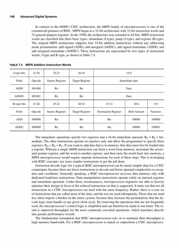
148 Advanced Digital Systems
In contrast to the 68000’s CISC architecture, the MIPS family of microprocessors is one of thecommercial pioneers of RISC. MIPS began as a 32-bit architecture with 32-bit instruction words and32 general-purpose registers. In the 1990s the architecture was extended to 64 bits. MIPS instructionwords are classified into three basic types: immediate (I-type), jump (J-type), and register (R-type).The original MIPS architecture supports four 32-bit addition instructions without any addressingmode permutations: add signed (ADD), add unsigned (ADDU), add signed immediate (ADDI), andadd unsigned immediate (ADDIU). These instructions are represented by two types of instructionwords, I-type and R-type, as shown in Table 7.4.
The immediate operations specify two registers and a 16-bit immediate operand: R
T
= R
S
+ Im-mediate. The other instructions operate on registers only and allow the programmer to specify threeregisters: R
D
= R
S
+ R
T
. If you want to add data that is in memory, that data must first be loaded intoa register. Whereas a single 68000 instruction can fetch a word from memory, increment the associ-ated pointer register, add the word to another register, and then store the result back into memory, aMIPS microprocessor would require separate instructions for each of these steps. This is in keepingwith RISC concepts: use more simpler instructions to get the job done.
Instruction decode logic for a typical RISC microprocessor can be much simpler than for a CISCcounterpart, because there are fewer instructions to decode and fewer operand complexities to recog-nize and coordinate. Generally speaking, a RISC microprocessor accesses data memory only withdedicated load/store instructions. Data manipulation instructions operate solely on internal registersand immediate operands. Under these circumstances, microprocessor engineers are able to heavilyoptimize their design in favor of the reduced instruction set that is supported. It turns out that not allinstructions in a CISC microprocessor are used with the same frequency. Rather, there is a core setof instructions that are called most of the time, and the rest are used infrequently. Those that are usedless often impose a burden on the entire system, because they increase the permutations that the de-code logic must handle in any given clock cycle. By removing the operations that are not frequentlyused, the microprocessor’s control logic is simplified and can therefore be made to run faster. The re-sult is improved throughput for the most commonly executed operations, which translates directlyinto greater performance overall.
The fundamental assumption that RISC microprocessors rely on to maintain their throughput ishigh memory bandwidth. For a RISC microprocessor to match or outperform a CISC microproces-
TABLE
7.4 MIPS Addition Instruction Words
I-type bits 31:26 25:21 20:16 15:0
Field Opcode Source Register Target Register Immediate data
ADDI 001000 Rn Rn Data
ADDIU 001001 Rn Rn Data
R-type bits 31:26 25:21 20:16 15:11 10:6 5:0
Field Opcode Source Register Target Register Destination Register Shift Amount Function
ADD 000000 Rn Rn Rn 00000 100000
ADDU 000000 Rn Rn Rn 00000 100001
-Balch.book Page 148 Thursday, May 15, 2003 3:46 PM

Advanced Microprocessor Concepts 149
sor, it must be able to rapidly fetch instructions, because several RISC instructions are necessary tomatch the capabilities of certain CISC instructions. An older computer architecture with an asyn-chronous memory interface may not be able to provide sufficient instruction bandwidth to make aRISC microprocessor efficient. CISC architectures dominated off-the-shelf microprocessor offeringsuntil low-latency memory subsystems became practical at a reasonable cost. Modern computer ar-chitectures implement very fast memory interfaces that are able to provide a steady stream of in-structions to RISC microprocessors.
One fundamental technique for improving the instruction fetch bandwidth is to design a micro-processor with two memory interfaces—one for instructions and one for data. This is referred to as a
Harvard
architecture, as compared to a conventional
von Neumann
architecture in which instructionand data memory are unified. Using a Harvard architecture, instruction fetches are not disrupted byload/store operations. Unfortunately, a Harvard architecture presents numerous system-level prob-lems of how to split program and data memory and how to load programs into memory that cannotbe accessed by load/store operations. Most microprocessors that implement a Harvard architecturedo so with smaller on-chip memory arrays that can store segments of program and data that arefetched from and written back to a unified memory structure external to the microprocessor chip.While this may sound so complex as to only be in the realm of serious number-crunchers, the smallbut powerful 8-bit PIC
TM
RISC microcontrollers from Microchip Technology implement a Harvardarchitecture with mutually exclusive program and data memory structures located on chip. This il-lustrates the point that advanced microprocessor concepts can be applied to any level of performanceif a problem needs to be solved.
The RISC concept appears to have won the day in the realm of high-performance computing.With memory bandwidth not being much of a hindrance, streamlined RISC designs can be made fastand efficient. In embedded computing applications, the victor is less clear. CISC technology is stillfirmly entrenched in a market where slow memory subsystems are still common and core micropro-cessor throughput is not always a major design issue. What is clear is that engineers and marketerswill continue to debate and turn out new products and literature to convince others why their ap-proach is the best available.
7.2 CACHE STRUCTURES
Microprocessor and memory performance have improved asymmetrically over time, leading to awell recognized performance gap. In 1980, a typical microprocessor ran at under 10 MHz, and a typ-ical DRAM exhibited an access time of about 250 ns. Two decades later, high-end microprocessorswere running at several hundred megahertz, and a typical DRAM exhibited an access time of 40 ns.Microprocessors’ appetites for memory bandwidth has increased by about two orders of magnitudeover 20 years while main memory technology, most often DRAM, has improved by less than an or-der of magnitude during that same period. To make matters worse, many microprocessors shiftedfrom CISC to RISC architectures during this same period, thereby further increasing their demandfor instruction memory bandwidth. The old model of directly connecting main memory to a micro-processor has broken down and become a performance-limiting bottleneck.
The culprits for slow main memory include the propagation delays through deep address decod-ing logic and the high random access latency of DRAM—the need to assert a row address, waitsome time, assert a column address, and wait some more time before data is returned. These prob-lems can be partially addressed by moving to SRAM. SRAM does not exhibit the latency penalty ofDRAM, but there are still the address decoding delays to worry about. It would be nice to build mainmemory with SRAM, but this is prohibitively expensive, as a result of the substantially lower den-
-Balch.book Page 149 Thursday, May 15, 2003 3:46 PM
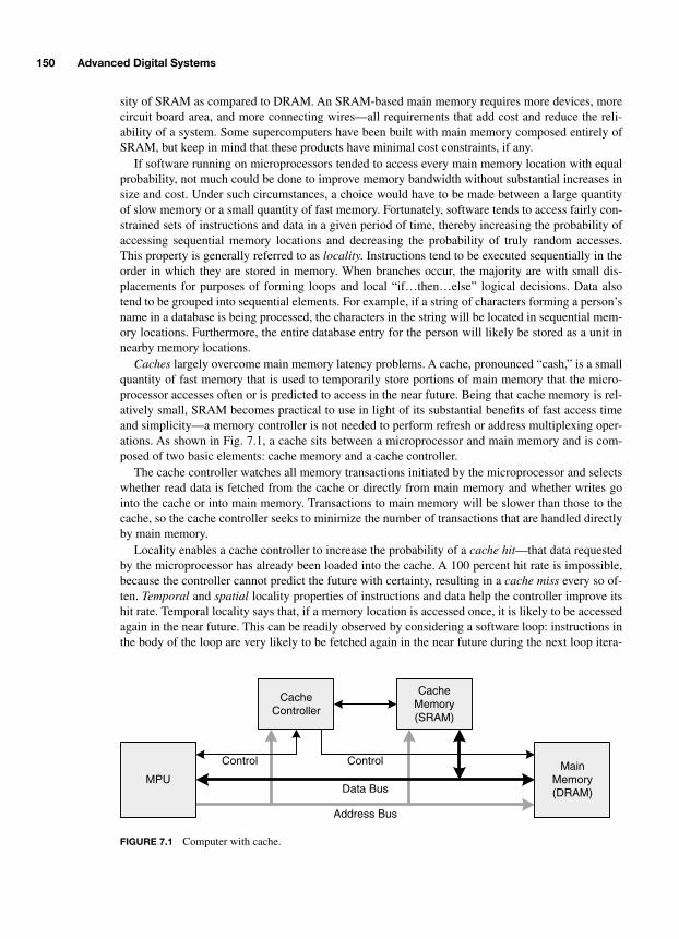
150 Advanced Digital Systems
sity of SRAM as compared to DRAM. An SRAM-based main memory requires more devices, morecircuit board area, and more connecting wires—all requirements that add cost and reduce the reli-ability of a system. Some supercomputers have been built with main memory composed entirely ofSRAM, but keep in mind that these products have minimal cost constraints, if any.
If software running on microprocessors tended to access every main memory location with equalprobability, not much could be done to improve memory bandwidth without substantial increases insize and cost. Under such circumstances, a choice would have to be made between a large quantityof slow memory or a small quantity of fast memory. Fortunately, software tends to access fairly con-strained sets of instructions and data in a given period of time, thereby increasing the probability ofaccessing sequential memory locations and decreasing the probability of truly random accesses.This property is generally referred to as
locality
. Instructions tend to be executed sequentially in theorder in which they are stored in memory. When branches occur, the majority are with small dis-placements for purposes of forming loops and local “if…then…else” logical decisions. Data alsotend to be grouped into sequential elements. For example, if a string of characters forming a person’sname in a database is being processed, the characters in the string will be located in sequential mem-ory locations. Furthermore, the entire database entry for the person will likely be stored as a unit innearby memory locations.
Caches
largely overcome main memory latency problems. A cache, pronounced “cash,” is a smallquantity of fast memory that is used to temporarily store portions of main memory that the micro-processor accesses often or is predicted to access in the near future. Being that cache memory is rel-atively small, SRAM becomes practical to use in light of its substantial benefits of fast access timeand simplicity—a memory controller is not needed to perform refresh or address multiplexing oper-ations. As shown in Fig. 7.1, a cache sits between a microprocessor and main memory and is com-posed of two basic elements: cache memory and a cache controller.
The cache controller watches all memory transactions initiated by the microprocessor and selectswhether read data is fetched from the cache or directly from main memory and whether writes gointo the cache or into main memory. Transactions to main memory will be slower than those to thecache, so the cache controller seeks to minimize the number of transactions that are handled directlyby main memory.
Locality enables a cache controller to increase the probability of a
cache hit
—that data requestedby the microprocessor has already been loaded into the cache. A 100 percent hit rate is impossible,because the controller cannot predict the future with certainty, resulting in a
cache miss
every so of-ten.
Temporal
and
spatial
locality properties of instructions and data help the controller improve itshit rate. Temporal locality says that, if a memory location is accessed once, it is likely to be accessedagain in the near future. This can be readily observed by considering a software loop: instructions inthe body of the loop are very likely to be fetched again in the near future during the next loop itera-
Address Bus
MPUMain
Memory(DRAM)
CacheMemory(SRAM)
CacheController
Data Bus
Control Control
FIGURE 7.1 Computer with cache.
-Balch.book Page 150 Thursday, May 15, 2003 3:46 PM
Advanced Microprocessor Concepts 151
tion. Spatial locality says that, if a memory location is accessed, it is likely that nearby locations willbe accessed in the near future. When a microprocessor fetches an instruction, there is a high proba-bility that it will soon fetch the instructions immediately following that instruction. Practicallyspeaking, temporal locality tells the cache controller to attempt to retain recently accessed memorylocations in the expectation that they will be accessed again. Spatial locality tells the cache control-ler to preload additional sequential memory locations when a single location is fetched by the micro-processor, in the expectation that these locations will be soon accessed.
Given the locality properties, especially spatial locality, that need to be incorporated into thecache controller, a basic cache organization emerges in which blocks of data rather than individualbytes are managed by the controller and held in cache memory. These blocks are commonly called
lines,
and they vary in size, depending on the specific implementation. Typical cache line sizes are16, 32, or 64 bytes. When the microprocessor reads a memory location that is not already locatedin the cache (a miss), the cache controller fetches an entire line from main memory and stores it asa unit. To maintain the simplicity of power-of-two logic, cache lines are typically mapped intomain memory on boundaries defined by the line size. A 16-byte cache line will always hold mem-ory locations at offsets represented by the four least-significant address bits. Main memory istherefore effectively divided into many small 16-byte lines with offsets from 0x0 to 0xF. If a micro-processor with a 32-bit address bus fetches location 0x1000800C and there is a cache miss, thecontroller will load locations 0x10008000 through 0x1000800F into a designated cache line. If thecache is full, and a miss occurs, the controller must
flush
a line that has a lower probability of useso as to make room for the new data. If the flushed line has been modified by writes that were notalready reflected in main memory, the controller must store the line to prevent losing and corrupt-ing the memory contents.
As more cache lines are implemented, more sections of main memory can be simultaneously heldin the cache, increasing the hit rate. However, a cache’s overall size must be bounded by a system’starget size and cost constraints. The size of a cache line is a compromise between granularity, load/store time, and locality benefits. For a fixed overall size, larger lines reduce the granularity of uniqueblocks of main memory that can be simultaneously held in the cache. Larger cache lines increase thetime required to load a new line and update main memory when flushing an old line. Larger cachelines also increase the probability that a subsequent access will result in a hit.
Cache behavior on reads is fairly consistent across different implementations. Writes, however,can be handled in one of three basic manners:
no-write
,
write-through
, and
write-back
. A no-writecache does not support the modification of its contents. When a write is performed to a block ofmemory held in a cache line, that line is flushed, and the write is performed directly into main mem-ory. This scheme imposes two penalties on the system: writes are always slowed by the longer la-tency of main memory, and locality benefits are lost because the flush forces any subsequentaccesses to that line to result in a miss and reload of the entire line that was already present in thecache.
Write-through caches support the modification of their contents but do not support incoherencybetween cache memory and main memory. Therefore, a write to a block of memory held in a cacheline results in a parallel write to both the cache and main memory. This is an improvement over a no-write cache in that the cache line is not forcibly flushed, but the write is still slowed by a direct ac-cess to main memory.
A write-back cache minimizes both penalties by enabling writes to valid cache lines but not im-mediately causing a write to main memory. The microprocessor does not have to incur the latencypenalty of main memory, because the write completes as fast as the cache can accept the new data.This scheme introduces complexity in the form of incoherency between cache and main memory:each memory structure has a different version of the same memory location. To solve the incoher-ency problem, a write-back cache must maintain a status bit for each line that indicates whether the
-Balch.book Page 151 Thursday, May 15, 2003 3:46 PM

152 Advanced Digital Systems
line is
clean
or
dirty
. When the line is eventually flushed, dirty lines must be written back to mainmemory in their entirety. Clean lines can be flushed without further action. While a write-back cachecannot absolutely eliminate the longer write latency of main memory, it can reduce the overall sys-tem impact of writes, because the microprocessor can perform any number of writes to the samecache line, and only a fixed write-back penalty results upon a flush.
The central problem in designing a cache is how to effectively hold many scattered blocks from alarge main memory in a small cache memory. In a standard desktop PC, main memory may consistof 256 MB of DRAM, whereas the microprocessor’s cache is 256 kB—a difference of three ordersof magnitude! The concept of cache lines provides a starting point with a defined granularity to min-imize the problem somewhat. Deciding on a 16-byte line size, for example, indicates that a 32-bitaddress space needs to be handled only as 2
28
units rather than 2
32
units. Of course, 2
28
is still a verylarge number! Each cache line must have an associated tag and/or index that identifies the higher-or-der address bits that its contents represent (28 bits in this example). Different cache architectureshandle these tags and indices to balance cache performance with implementation expense. The threestandard cache architectures are
fully associative
,
direct mapped
, and
n-way set associative
.A fully associative cache, shown in Fig. 7.2, breaks the address bus into two sections: the lower
bits index into a selected cache line to select a byte within the line, and the upper bits form a tag thatis associated with each cache line. Each cache line contains a valid bit to indicate whether it containsreal data. Upon reset, the valid bits for each line are cleared to 0. When a cache line is loaded withdata, its tag is set to the high-order address bits that are driven by the microprocessor. On subsequenttransactions, those address bits are compared in parallel against every tag in the cache. A hit occurswhen one tag matches the requested address, resulting in that line’s data advancing to a final multi-plexer where the addressed bytes are selected by the low-order address bits. A fully associativecache is the most flexible type, because any cache line can hold any portion of main memory. Thedisadvantage of this scheme is its complexity of implementation. Each line requires address match-
A[31:4] A[3:0]
requested address
Byt
e se
lect
RequestedData
28-bit line tag 16-byte line datavalid
=
Z
match
28-bit line tag 16-byte line datavalid
=
Z
match
Hit28-bit line tag 16-byte line datavalid
=
Z
match
28-bit line tag 16-byte line datavalid
=
Z
match
FIGURE 7.2 Fully associative cache.
-Balch.book Page 152 Thursday, May 15, 2003 3:46 PM

Advanced Microprocessor Concepts 153
ing logic, and each match signal must be logically combined in a single location to generate a finalhit/miss status flag.
A direct mapped cache, shown in Fig. 7.3, breaks the address bus into three sections; the lowerbits retain their index function within a selected line, the middle bits select a single line from an ar-ray of uniquely addressable lines, and the upper bits form a tag to match the selected cache line. Asbefore, each cache line contains a valid bit. The difference here is that each block of memory canonly be mapped into one cache line—the one indexed by that block’s middle address bits, A[15:4] inthis example (indicating a 64-kB total cache size). During a cache miss, the controller determineswhich line is selected by the middle address bits, loads the line, sets the valid bit, and loads the linetag with the upper address bits. On subsequent accesses, the middle address bits select a single linewhose tag is compared against the upper address bits. If they match, there is a cache hit. A directmapped cache is much easier to implement as compared to a fully associative cache, because paral-lel tag matching is not required. Instead, the cache can be constructed with conventional memoryand logic components using off-the-shelf RAM for both the tag and line data. The control logic canindex into the RAM, check the selected tag for a match, and then take appropriate action. The disad-vantage to a direct mapped cache is that, because of the fixed mapping of memory blocks to cachelines, certain data access patterns can cause rapid
thrashing
. Thrashing results when the micropro-cessor rapidly accesses alternate memory blocks. If the alternate blocks happen to map to the samecache line, the cache will almost always miss, because each access will result in a flush of the alter-nate memory block.
Given the simplicity of a direct mapped cache, it would be nice to strike a compromise betweenan expensive fully associative cache and a thrashing-sensitive direct mapped cache. The
n-way
setassociative cache is such a compromise. As shown in Fig. 7.4, a two-way set associative cache isbasically two direct mapped cache elements connected in parallel to reduce the probability ofthrashing. More than two sets can be implemented to further reduce thrashing potential. Four-wayand two-way set associative caches are very common in modern computers. Beyond four ele-ments, the payback of thrashing avoidance to implementation complexity declines. The term
set
refers to the number of entries in each direct mapped element, 4,096 in this example. Here, the
requested address
Byt
e se
lect
RequestedData
A[31:16] A[3:0]A[15:4]
16-bit line tag 16-byte line datavalid
16-bit line tag 16-byte line datavalid
16-bit line tag 16-byte line datavalid
16-bit line tag 16-byte line datavalid
=
Cache Tag and Data RAM: 4,096 entries
RAMIndex
Hit
FIGURE 7.3 64-kB direct mapped cache.
-Balch.book Page 153 Thursday, May 15, 2003 3:46 PM

154 Advanced Digital Systems
cache has expanded to 128 kB in size using two 64 kB elements. If cost constraints dictate keepinga 64 kB cache, it would be preferable to reduce the set size to 2,048 rather than halve the line size,which is already at a practical minimum of 16 bytes. Reducing the set size to 2
11
would increasethe line tag to 17 bits to maintain a 32-bit address space representation. In a cache of this type, thecontroller can choose which of two (or four, or
n
) cache line locations to flush when a miss is en-countered.
Deciding which line to flush when a cache miss occurs can be done in a variety of ways, and dif-ferent cache architectures dictate varying approaches to this problem. A fully associative cache canplace any main memory block into any line, while a direct mapped cache has only one choice forany given memory block. Three basic flush, or replacement, algorithms are as follows:
•
First-in-first-out (FIFO).
Track cache line ages and replace the oldest line.
•
Least-recently-used (LRU).
Track cache line usage and replace the line that has not been ac-cessed longest.
•
Random.
Replace a random line.
A fully associative cache has the most flexibility in selecting cache lines and therefore the mostcomplexity in tracking line usage. To perform either a FIFO or LRU replacement algorithm on afully associative cache, each line would need a tracking field that could be updated and checked inparallel with all other lines. N-way set associative caches are the most interesting problems from apractical perspective, because they are used most frequently. Replacement algorithms for thesecaches are simplified, because the number of replacement choices is restricted to N. A two-way setassociative cache can implement either FIFO or LRU algorithms with a single bit per line entry.For a FIFO algorithm, the entry being loaded anew has its FIFO bit cleared, and the other entry hasits FIFO bit set, indicating that the other entry was loaded first. For an LRU algorithm, the entry be-ing accessed at any given time has its LRU bit cleared, and the other has its LRU bit set, indicatingthat the other entry was used least recently. These algorithms and associated hardware are only
Hit
=
16-bit tag 16-byte dataV
16-bit tag 16-byte dataVZ
Byt
e se
lect
RequestedData
requested address
A[31:16] A[3:0]A[15:4]
=
16-bit tag 16-byte dataV
16-bit tag 16-byte dataVZ
FIGURE 7.4 128-kB two-way set associative cache.
-Balch.book Page 154 Thursday, May 15, 2003 3:46 PM
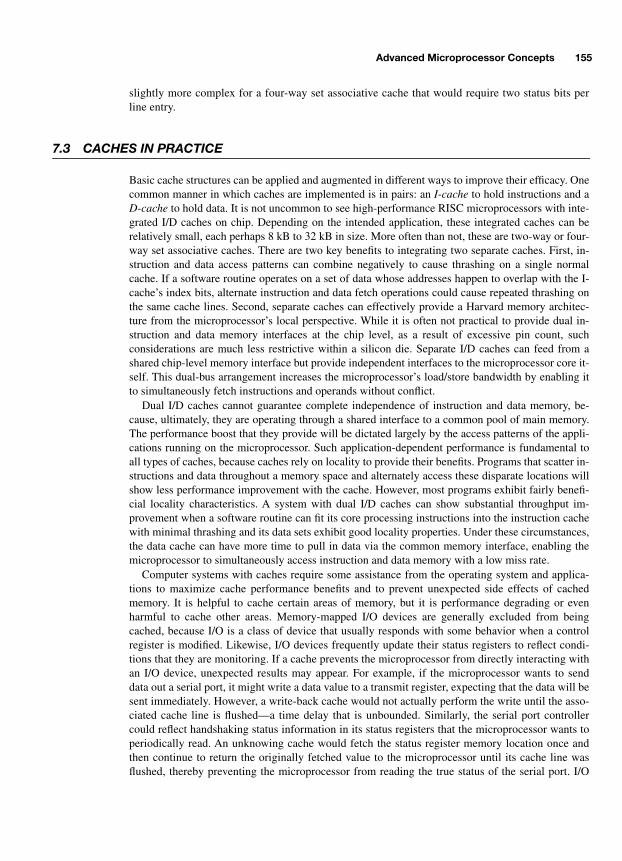
Advanced Microprocessor Concepts 155
slightly more complex for a four-way set associative cache that would require two status bits perline entry.
7.3 CACHES IN PRACTICE
Basic cache structures can be applied and augmented in different ways to improve their efficacy. Onecommon manner in which caches are implemented is in pairs: an
I-cache
to hold instructions and a
D-cache
to hold data. It is not uncommon to see high-performance RISC microprocessors with inte-grated I/D caches on chip. Depending on the intended application, these integrated caches can berelatively small, each perhaps 8 kB to 32 kB in size. More often than not, these are two-way or four-way set associative caches. There are two key benefits to integrating two separate caches. First, in-struction and data access patterns can combine negatively to cause thrashing on a single normalcache. If a software routine operates on a set of data whose addresses happen to overlap with the I-cache’s index bits, alternate instruction and data fetch operations could cause repeated thrashing onthe same cache lines. Second, separate caches can effectively provide a Harvard memory architec-ture from the microprocessor’s local perspective. While it is often not practical to provide dual in-struction and data memory interfaces at the chip level, as a result of excessive pin count, suchconsiderations are much less restrictive within a silicon die. Separate I/D caches can feed from ashared chip-level memory interface but provide independent interfaces to the microprocessor core it-self. This dual-bus arrangement increases the microprocessor’s load/store bandwidth by enabling itto simultaneously fetch instructions and operands without conflict.
Dual I/D caches cannot guarantee complete independence of instruction and data memory, be-cause, ultimately, they are operating through a shared interface to a common pool of main memory.The performance boost that they provide will be dictated largely by the access patterns of the appli-cations running on the microprocessor. Such application-dependent performance is fundamental toall types of caches, because caches rely on locality to provide their benefits. Programs that scatter in-structions and data throughout a memory space and alternately access these disparate locations willshow less performance improvement with the cache. However, most programs exhibit fairly benefi-cial locality characteristics. A system with dual I/D caches can show substantial throughput im-provement when a software routine can fit its core processing instructions into the instruction cachewith minimal thrashing and its data sets exhibit good locality properties. Under these circumstances,the data cache can have more time to pull in data via the common memory interface, enabling themicroprocessor to simultaneously access instruction and data memory with a low miss rate.
Computer systems with caches require some assistance from the operating system and applica-tions to maximize cache performance benefits and to prevent unexpected side effects of cachedmemory. It is helpful to cache certain areas of memory, but it is performance degrading or evenharmful to cache other areas. Memory-mapped I/O devices are generally excluded from beingcached, because I/O is a class of device that usually responds with some behavior when a controlregister is modified. Likewise, I/O devices frequently update their status registers to reflect condi-tions that they are monitoring. If a cache prevents the microprocessor from directly interacting withan I/O device, unexpected results may appear. For example, if the microprocessor wants to senddata out a serial port, it might write a data value to a transmit register, expecting that the data will besent immediately. However, a write-back cache would not actually perform the write until the asso-ciated cache line is flushed—a time delay that is unbounded. Similarly, the serial port controllercould reflect handshaking status information in its status registers that the microprocessor wants toperiodically read. An unknowing cache would fetch the status register memory location once andthen continue to return the originally fetched value to the microprocessor until its cache line wasflushed, thereby preventing the microprocessor from reading the true status of the serial port. I/O
-Balch.book Page 155 Thursday, May 15, 2003 3:46 PM

156 Advanced Digital Systems
registers are unlike main memory, because memory just holds data and cannot modify it or take ac-tions based on it.
Whereas caching an I/O region can cause system disruption, caching certain legitimate main mem-ory regions can cause performance degradation due to thrashing. It may not be worth caching smallroutines that are infrequently executed, because the performance benefit of caching a quick mainte-nance routine may be small, and its effect on flushing more valuable cache entries may significantlyslow down the application that resumes execution when the maintenance routine completes. A perfor-mance-critical application is often composed of a processing kernel along with miscellaneous initial-ization and maintenance routines. Most of the microprocessor time is spent executing kernelinstructions, but sometimes the kernel must branch to maintenance routines for purposes such as load-ing or storing data. Unlike I/O regions that are inherently known to be cache averse, memory regionsthat should not be cached can only be known by the programmer and explicitly kept out of the cache.
Methods of excluding certain memory locations from the cache differ across system implementa-tions. A cache controller will often contain a set of registers that enable the lockout of specificmemory regions. On those integrated microprocessors that contain some address decoding logic aswell as a cache controller, individual memory areas are configured into the decoding logic with pro-grammable registers, and each is marked as cacheable or noncacheable. When the microprocessorperforms a memory transaction, the address decoder sends a flag to the cache controller that tells itwhether to participate in the transaction.
On the flip side of locking certain memory regions out of the cache, some applications can benefitfrom explicitly locking certain memory regions into the cache. Locking cache entries prevents thecache controller from flushing those entries when a miss occurs. A programmer may be able to locka portion of the processing kernel into the cache to prevent arbitrary maintenance routines from dis-turbing the most frequently accessed sets of instructions and data.
Cache controllers perform burst transactions to main memory because of their multiword line ar-chitecture. Whether the cache is reading a new memory block on a cache miss or writing a dirty blockback to main memory, its throughput is greatly increased by performing burst transfers rather thanreading or writing a single word at a time. Normal memory transfers are executed by presenting an ad-dress and reading or writing a single unit of data. Each type of memory technology has its own associ-ated latency between the address and data phases of a transaction. SRAM is characterized by very lowaccess latency, whereas DRAM has a higher latency. Because main memory in most systems is com-posed of DRAM, single-unit memory transfers are inefficient, because each byte or word is penalizedby the address phase overhead. Burst transfers, however, return multiple sequential data units whilerequiring only an initial address presentation, because the address specifies a starting address for a setof memory locations. Therefore, the overhead of the address phase is amortized across many dataunits, greatly increasing the efficiency of the memory system. Modern DRAM devices support bursttransfers that nicely complement the cache controllers that often coexist in the same computer system.
As a result of cache subsystems being integrated onto the same chip along with high-performancemicroprocessors, the external memory interface is less a microprocessor bus and more a burst-modecache bus. The microprocessor needs to be able to bypass the cache controller while accessing non-cacheable memory locations or during boot-up when peripherals such as the cache controller havenot yet been initialized. However, the external bus is often optimized for burst transfers, and absoluteefficiency or simplicity when dealing with noncacheable locations may be a secondary concern tothe manufacturer. If overall complexity can be reduced by giving up some performance in nonbursttransfers, it may be worth the trade-off, because high performance microprocessors spend relativelylittle of their time accessing external memory directly. If they do, then something is wrong with thesystem design, because the microprocessor’s throughput is sure to suffer.
Many microprocessors are designed to support multiple levels of caching to further improve per-formance. In this context, the cache that is closest to the microprocessor core is termed a
level-one
-Balch.book Page 156 Thursday, May 15, 2003 3:46 PM
Advanced Microprocessor Concepts 157
(L1) cache. The L1 cache is fairly small, anywhere from 2 kB to 64 kB, with its benefit being speed.Because it is small and close to the microprocessor, it can be made to run as fast as the microproces-sor can fetch instructions and data. Instruction and data caches are implemented at L1. Line sizes forL1 caches vary but are often 16 or 32 bytes. The line size needs to be kept to a practical minimum tomaximize the number of unique memory blocks that can be stored in a small RAM structure.
Level two (L2) caches may reside on the same silicon chip as the microprocessor and L1 cache orexternally to the chip, depending on the implementation. L2 caches are generally unified instructionand data caches to minimize the complexity of the interface between the L1 cache and the rest of thesystem. These caches run somewhat slower than L1 but, consequently, they can be made larger:128 kB, 256 kB, or more. Line sizes of 64 bytes and greater are common in L2 caches to increase ef-ficiency of main memory burst transfers. Because the L2 cache has more RAM, it can expand boththe number of lines and the line size in the hope that, when the L1 cache requests a block of memory,the next sequential block will soon be requested as well. Beyond L2, some microprocessors supportL3 and even L4 caches. Each successive level increases its latency of response to the cache above itbut adds more cache RAM (sometimes megabytes) and sometimes larger line sizes to increase burst-mode transfer efficiency to main memory.
As core microprocessor clock frequencies commonly top several hundred megahertz, and themost advanced microprocessors exceed 1 GHz, the bandwidth disparity between the microprocessorand main memory increases. Cache misses impose severe penalties on throughput, because the ef-fective clock speed of the microprocessor is essentially reduced to that of the memory subsystemwhen data is fetched directly from memory. The goal of a multilevel cache structure is to substan-tially reduce the probability of a cache miss that leads directly to main memory. If the L1 cachemisses, hopefully, the L2 cache will be ready to supply the requested data at only a moderatethroughput penalty.
Caching as a concept is not restricted to the context of microprocessors and hardware implemen-tation. Caches are found in hard disk drives and in Internet caching products. Some high-end harddrives implement several megabytes of RAM to prefetch data beyond that which has already beenrequested. While the hard drive’s cache, possibly implemented using DRAM, is not nearly as fast asa typical microprocessor, it is orders of magnitude faster than the drive mechanism itself. Internetcaching products routinely copy commonly accessed web sites and other data onto their hard drivesso that subsequent accesses do not have to go all the way out to the remote file server. Instead, the re-quested data is sitting locally on a cache system. Caching is the general concept of substituting asmall local storage resource that is faster than the larger more remote resource. Caches can be ap-plied in a wide variety of situations.
Caching gets somewhat more complex when the data that is being cached can be modified by an-other entity outside of the cache memory. This is possible in the Internet caching application men-tioned above or in a multiprocessor computer. Cache coherency is the subject of many researchpapers and is a problem that needs to be addressed by each implementation. Simply put, how doesthe Internet cache know when a web site that is currently stored has been updated? A news web site,for example, may update its contents every few hours. In a multiprocessor context, multiple micro-processors may have access to the same pool of shared memory. Here, the multiple cache controllersmust somehow communicate to know when memory has been modified so that the individual cachescan update themselves and maintain coherency.
Determining the optimal size of a cache so that its performance improvement merits its cost hasbeen the subject of much study. Cache performance is highly application dependent and, in general,meaningful performance improvements decline after a certain size threshold, which varies by appli-cation. A typical PC runs programs that are not very computationally intensive and that operate onlimited sets of data over short time intervals. In short, they exhibit fairly good locality properties.Typical desktop PCs contain 256 kB of L2 cache and a smaller quantity of L1 cache. Computers that
-Balch.book Page 157 Thursday, May 15, 2003 3:46 PM

158 Advanced Digital Systems
often operate on larger sets of data or that must run many applications simultaneously may meritlarger caches to offset less optimal locality properties. Computers meant to function as computationengines and network file servers can include several megabytes of L2 cache. Smaller embedded sys-tems may suffice with only several kilobytes of L1 cache.
7.4 VIRTUAL MEMORY AND THE MMU
Multitasking operating systems execute multiple programs at the same time by assigning each pro-gram a certain percentage of the microprocessor’s time and then periodically changing which in-struction sequence is being executed. This is accomplished by a periodic timer interrupt that causesthe OS kernel to save the state of the microprocessor’s registers and then reload the registers withpreserved state from a different program. Each program runs for a while and is paused, after whichexecution resumes without the program having any knowledge of having been paused. In this re-spect, the individual programs in a multitasking environment appear to have complete control overthe computer, despite sharing the resources with others. Such a perspective makes programming fora multitasking OS easier, because the programmer does not have to worry about the infinite permuta-tions of other applications that may be running at any given time. A program can be written as if it isthe only application running, and the OS kernel sorts out the run-time responsibilities of making surethat each application gets fair time to run on the microprocessor.
Aside from fair access to microprocessor time, conflicts can arise between applications that acci-dentally modify portions of each other’s memory—either program or data. How does an applicationknow where to locate its data so that it will not disturb that of other applications and so that it willnot be overwritten? There is also the concern about system-wide fault tolerance. Even if not mali-cious, programs may have bugs that cause them to crash and write data to random memory locations.In such an instance, one errant application could bring down others or even crash the OS if it over-writes program and data regions that belong to the OS kernel. The first problem can be addressedwith the honor system by requiring each application to dynamically request memory allocations atrun time from the kernel. The kernel can then make sure that each application is granted an exclusiveregion of memory. However, the second problem of errant writes requires a hardware solution thatcan physically prevent an application from accessing portions of memory that do not belong to it.
Virtual memory is a hardware enforced and software configured mechanism that provides eachapplication with its own private memory space that it can use arbitrarily. This virtual memory spacecan be as large as the microprocessor’s addressing capability—a full 4 GB in the case of a 32-bit mi-croprocessor. Because each application has its own exclusive virtual memory space, it can use anyportion of that space that is not otherwise restricted by the kernel. Virtual memory frees the program-mer from having to worry about where other applications may locate their instructions or data, be-cause applications cannot access the virtual memory spaces of others. In fact, operating systems thatsupport virtual memory may simplify the physical structure of programs by specifying a fixed start-ing address for instructions, the local stack, and data. UNIX is an example of an OS that does this.Each application has its instructions, stack, and data at the same virtual addresses, because they haveseparate virtual memory spaces that are mutually exclusive and, therefore, not subject to conflict.
Clearly, multiple programs cannot place different data at the same address or each simultaneouslyoccupy the microprocessor’s entire address space. The OS kernel configures a hardware memorymanagement unit (MMU) to map each program’s virtual addresses into unique physical addressesthat correspond to actual main memory. Each unique virtual memory space is broken into manysmall pages that are often in the range of 2 to 16 kB in size (4 kB is a common page size). The OSand MMU refer to each virtual memory space with a process ID (PID) field. Virtual memory is han-
-Balch.book Page 158 Thursday, May 15, 2003 3:46 PM

Advanced Microprocessor Concepts 159
dled on a process basis rather than an application basis, because it is possible for an application toconsist of multiple semi-independent processes. The high-order address bits referenced by each in-struction form the virtual page number (VPN). The PID and VPN are combined to uniquely map toa physical address set aside by the kernel as shown in Fig. 7.5. Low-order address bits represent off-sets that directly index into mapped pages in physical memory. The mapping of virtual memorypages into physical memory is assigned arbitrarily by the OS kernel. The kernel runs in real memoryrather than in virtual memory so that it can have direct access to the computer’s physical resources toallocate memory as individual processes are executed and then terminated.
Despite each process having a 4-GB address space, virtual memory can work on computers withjust megabytes of memory, because the huge virtual address spaces are sparsely populated. Mostprocesses use only a few hundred kilobytes to a few megabytes of memory and, therefore, multipleprocesses that collectively have the potential to reference tens of gigabytes can be mapped into amuch smaller quantity of real memory. If too many processes are running simultaneously, or if theseprocesses start to consume too much memory, a computer can exhaust its physical memory re-sources, thereby requiring some intervention from the kernel to either suspend a process or handlethe problem in some other way.
When a process is initiated, or spawned, it is assigned a PID and given its own virtual memoryspace. Some initial pages are allocated to hold its instructions and whatever data memory the pro-cess needs available when it begins. During execution, processes may request more memory fromthe kernel by calling predefined kernel memory management routines. The kernel will respond byallocating a page in physical memory and then returning a pointer to that page’s virtual mapping.Likewise, a process can free a memory region when it no longer needs it. Under this circumstance,the kernel will remove the mapping for the particular pages, enabling them to be reallocated to an-other process, or the same process, at a later time. Therefore, the state of memory in a typical multi-tasking OS is quite dynamic, and the routines to manage memory must be implemented in softwarebecause of their complexity and variability according to the platform and the nature of processesrunning at any given time.
Not all mapped virtual memory pages have to be held in physical RAM at the same time. Instead,the total virtual memory allocation on a computer can spill over into a secondary storage mediumsuch as a hard drive. The hard drive will be much slower than DRAM, but not every memory page inevery process is used at the same time. When a process is first loaded, its entire instruction image istypically loaded into virtual memory. However, it will take some time for all of those instructions toreach their turn in the execution sequence. During this wait time, the majority of a process’s program
PID1
4-GB VirtualAddress Space
PID2
unusedpages
unusedpages
4-GB PhysicalAddress Space
4-GB VirtualAddress Space
unusedmemory
kernel
FIGURE 7.5 32-bit virtual memory mapping.
-Balch.book Page 159 Thursday, May 15, 2003 3:46 PM

160 Advanced Digital Systems
memory can be stored on the hard drive without incurring a performance penalty. When those in-structions are ready to be executed, the OS kernel will have to transfer the data into physical mem-ory. This slows the system down but makes it more flexible without requiring huge quantities ofDRAM. Part of the kernel’s memory management function is to decide which virtual pages shouldbe held in DRAM and which should be swapped out to the disk. Pages that have not been used for awhile can be swapped out to make room for new pages that are currently needed. If a process subse-quently accesses a page that has been moved to the disk, that page can be swapped back into DRAMto replace another page that is not needed at the time. A computer with 256 MB of DRAM could, forexample, have a 512-MB swap file on its hard drive, enabling processes to share a combined768 MB of used virtual memory.
This scheme of expanding virtual memory onto a disk effectively turns the computer’s DRAMinto a large cache for an even larger disk-based memory. As with all caches, certain behavioral char-acteristics exist. A virtual memory page that is not present in DRAM is effectively a cache misswith a large penalty, because hard disks are much slower than DRAM. Such misses are called pagefaults. The MMU detects that the requested virtual memory address from a particular PID is notpresent in DRAM and causes an exception that must be handled by the OS kernel. Instead of per-forming a cache line fill and flush, it is the kernel’s responsibility to swap pages to and from thedisk. For a virtual memory system to function with reasonable performance, the working set ofmemory across all the processes running should be able to fit into the computer’s physical memory.The working set includes any instructions and data that are accessed within a local time interval.This is directly analogous to a microprocessor cache’s exploitation of locality. Processes with goodlocality characteristics will do well in a cache and in a virtual memory system. Processes with poorlocality may result in thrashing as many sequential page faults are caused by random accessesthroughout a large virtual memory space.
The virtual to physical address mapping process is guided by the kernel using a page table,which can take various forms but must somehow map each PID/VPN combination to either a phys-ical memory page or one located on the disk drive’s swap area. Virtual page mapping is illustratedin Fig. 7.6, assuming 4-kB pages, a 32-bit address space, and an 8-bit PID. In addition to basic map-ping information, the page table also contains status information, including a dirty bit that indicateswhen a page held in memory has been modified. If modified, the page must be saved to the disk be-fore being flushed to make room for a new virtual page. Otherwise, the page can be flushed withoutfurther action.
Given a 4-kB page size and a 32-bit address space, each process has access to 220 = 1,048,576pages. With 256 PIDs, a brute-force page table would contain more than 268 million entries! Thereare a variety of schemes to reduce page table size, but there is no escaping the fact that a page table
A[31:12] A[11:0]
VPN Offset
PID[7:0]
Page Table
A[31:12]
Physical Page Address
A[11:0]
Offset
FIGURE 7.6 Virtual page mapping.
-Balch.book Page 160 Thursday, May 15, 2003 3:46 PM

Advanced Microprocessor Concepts 161
will be large. Page table management schemes are largely an issue of OS architecture and are out-side the scope of this discussion. The fact that the page table is large and is parsed by softwaremeans that the mapping process will be extremely slow without hardware assistance. Every access tovirtual memory, in other words almost every access performed on the computer, requires mapping,which makes hardware acceleration critical to the viability of virtual memory.
Within the MMU is a translation lookaside buffer (TLB), a small, fully associative cache that al-lows the MMU to rapidly locate recently accessed virtual page mappings. Typical sizes for a TLBare just 16 to 64 entries because of the complexity of implementing a fast fully associative cache.When a process is first spawned, it has not yet performed virtual memory accesses, so its first accesswill result in a TLB miss. When a TLB miss occurs, an exception is generated that invokes the ker-nel’s memory management routine to parse the page table in search of the correct physical addressmapping. The kernel routine loads a TLB entry with the mapping information and exits. On subse-quent memory accesses, the TLB will hit some and miss some. It is hoped that the ratio of hits tomisses will decline rapidly as the process executes. Once again, locality of reference is key to a wellperforming application, but the TLB and MMU are not as sensitive to locality as a normal cache, be-cause they map multiple-kilobyte pages rather than 16 or 32 byte lines. Yet, as more processes ac-tively vie for resources in a multitasking system, they may begin to fight each other for scarce TLBentries. The resources and architecture of a computer must be properly matched to its intended appli-cation. A typical desktop or embedded computer may get along fine with a small TLB, because itmay not have many demanding processes running concurrently. A more powerful computer de-signed to simultaneously run many memory-intensive processes may require a larger TLB to takefull advantage of its microprocessor and memory resources. The ever-present trade-off between per-formance and cost does not go away!
The TLB is usually located between the microprocessor and its cache subsystem as shown in Fig.7.7, such that physical addresses are cached rather than virtual addresses. Such an arrangement addslatency to microprocessor transactions, because the virtual-to-physical mapping must take place be-fore the L1 cache can respond. A TLB can be made very fast because of its small size, thereby limit-ing its time penalty on transactions. Additionally, microprocessors may implement a pipelinedinterface where addresses are presented each clock cycle, but their associated data are returned oneor more clock cycles later, providing time for the TLB lookup.
7.5 SUPERPIPELINED AND SUPERSCALAR ARCHITECTURES
At any given time, semiconductor process technology presents an intrinsic limitation on how fast alogic gate can switch on and off and at what frequency a flip-flop can run. Other than relying onsemiconductor process advances to improve microprocessor and system throughput, certain basictechniques have been devised to extract more processing power from silicon with limited switching
Address
PhysicalPagePID/VPN
MPUL2 Cache/
DRAM
MMU
TLBTLB Miss L1 Cache
Page Offset
FIGURE 7.7 Location of TLB.
-Balch.book Page 161 Thursday, May 15, 2003 3:46 PM

162 Advanced Digital Systems
delays. Throughput can be enhanced in a serial manner by trying to execute a desired function faster.If each function is executed at a faster clock frequency, more functions can be executed in a giventime period. An alternative parallel approach can be taken whereby multiple functions are executedsimultaneously, thereby improving performance over time. These two approaches can be comple-mentary in practice. Different logic implementations make use of serial and parallel enhancementtechniques in the proportions and manners that are best suited to the application at hand.
A logic function is represented by a set of Boolean equations that are then implemented as dis-crete gates. During one clock cycle, the inputs to the equations are presented to a collection of gatesvia a set of input flops, and the results are clocked into output flops on the next rising edge. Thepropagation delays of the gates and their interconnecting wires largely determine the shortest clockperiod at which the logic function can reliably operate.
Pipelining, called superpipelining when taken to an extreme, is a classic serial throughput en-hancement technique. Pipelining is the process of breaking a Boolean equation into several smallerequations and then calculating the partial results during sequential clock cycles. Smaller equationsrequire fewer gates, which have a shorter total propagation delay relative to the complete equation.The shorter propagation delay enables the logic to run faster. Instead of calculating the complete re-sult in a single 40 ns cycle, for example, the result may be calculated in four successive cycles of10 ns each. At first glance, it may not seem that anything has been gained, because the calculationstill takes 40 ns to complete. The power of pipelining is that different stages in the pipeline are oper-ating on different calculations each cycle. Using an example of an adder that is pipelined across fourcycles, partial sums are calculated at each stage and then passed to the next stage. Once a partial sumis passed to the next stage, the current stage is free to calculate the partial sum of a completely newaddition operation. Therefore, a four-stage pipelined adder takes four cycles to produce a result, butit can work on four separate calculations simultaneously, yielding an average throughput of one cal-culation every cycle—a four-times throughput improvement.
Pipelining does not come for free, because additional logic must be created to handle the com-plexity of tracking partial results and merging them into successively more complete results. Pipelin-ing a 32-bit unsigned integer adder can be done as shown in Fig. 7.8 by adding eight bits at a timeand then passing the eight-bit sum and carry bit up to the next stage. From a Boolean equation per-spective, each stage only incurs the complexity of an 8-bit adder instead of a 32-bit adder, enabling itto run faster. An array of pipeline registers is necessary to hold the partial sums that have been calcu-lated by previous stages and the as-yet-to-be-calculated portions of the operands. The addition re-sults ripple through the pipeline on each rising clock edge and are accumulated into a final 32-bitresult as operand bytes are consumed by the adders. There is no feedback in this pipelined adder,meaning that, once a set of operands passes through a stage, that stage no longer has any involve-ment in the operation and can be reused to begin or continue a new operation.
Pipelining increases the overall throughput of a logic block but does not usually decrease the cal-culation latency. High-performance microprocessors often take advantage of pipelining to varyingdegrees. Some microprocessors implement superpipelining whereby a simple RISC instruction mayhave a latency of a dozen or more clock cycles. This high degree of pipelining allows the micropro-cessor to execute an average of one instruction each clock cycle, which becomes very powerful atoperating frequencies measured in hundreds of megahertz and beyond.
Superpipelining a microprocessor introduces complexities that arise from the interactions be-tween consecutive instructions. One instruction may contain an operand that is calculated by the pre-vious instruction. If not handled correctly, this common circumstance can result in the wrong valuebeing used in a subsequent instruction or a loss of performance where the pipeline is frequentlystalled to allow one instruction to complete before continuing with others. Branches can also causehavoc with a superpipelined architecture, because the decision to take a conditional branch may nul-lify the few instructions that have already been loaded into the pipeline and partially executed. De-
-Balch.book Page 162 Thursday, May 15, 2003 3:46 PM
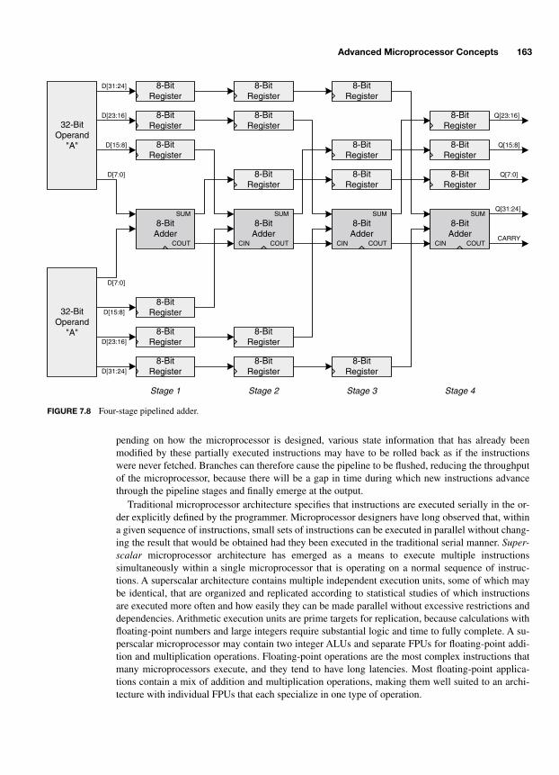
Advanced Microprocessor Concepts 163
pending on how the microprocessor is designed, various state information that has already beenmodified by these partially executed instructions may have to be rolled back as if the instructionswere never fetched. Branches can therefore cause the pipeline to be flushed, reducing the throughputof the microprocessor, because there will be a gap in time during which new instructions advancethrough the pipeline stages and finally emerge at the output.
Traditional microprocessor architecture specifies that instructions are executed serially in the or-der explicitly defined by the programmer. Microprocessor designers have long observed that, withina given sequence of instructions, small sets of instructions can be executed in parallel without chang-ing the result that would be obtained had they been executed in the traditional serial manner. Super-scalar microprocessor architecture has emerged as a means to execute multiple instructionssimultaneously within a single microprocessor that is operating on a normal sequence of instruc-tions. A superscalar architecture contains multiple independent execution units, some of which maybe identical, that are organized and replicated according to statistical studies of which instructionsare executed more often and how easily they can be made parallel without excessive restrictions anddependencies. Arithmetic execution units are prime targets for replication, because calculations withfloating-point numbers and large integers require substantial logic and time to fully complete. A su-perscalar microprocessor may contain two integer ALUs and separate FPUs for floating-point addi-tion and multiplication operations. Floating-point operations are the most complex instructions thatmany microprocessors execute, and they tend to have long latencies. Most floating-point applica-tions contain a mix of addition and multiplication operations, making them well suited to an archi-tecture with individual FPUs that each specialize in one type of operation.
32-BitOperand
"A"
D[31:24]
32-BitOperand
"A"
D[23:16]
D[15:8]
D[7:0]
D[7:0]
D[31:24]
D[23:16]
D[15:8]
Q[31:24]
Q[23:16]
Q[15:8]
Q[7:0]
CARRY
8-BitRegister
8-BitAdder
COUT
SUM
CIN
8-BitRegister
8-BitRegister
8-BitRegister
8-BitRegister
8-BitRegister
8-BitRegister
8-BitRegister
8-BitRegister
8-BitRegister
8-BitRegister
8-BitRegister
8-BitRegister
8-BitRegister
8-BitRegister
8-BitRegister
8-BitRegister
8-BitRegister
Stage 1 Stage 2 Stage 3 Stage 4
8-BitAdder
COUT
SUM
CIN
8-BitAdder
COUT
SUM
8-BitAdder
COUT
SUM
CIN
FIGURE 7.8 Four-stage pipelined adder.
-Balch.book Page 163 Thursday, May 15, 2003 3:46 PM

164 Advanced Digital Systems
Managing parallel execution units in a superscalar microprocessor is a complex task, because themicroprocessor wants to execute instructions as fast as they can be fetched—yet it must do so in amanner consistent with the instructions’ serial interdependencies. These dependencies can becomemore complicated to resolve when superscalar and superpipelining techniques are combined to cre-ate a microprocessor with multiple execution units, each of which is implemented with a deep pipe-line. In such chips, the instruction decode logic handles the complex task of examining the pipelinesof the execution units to determine when the next instruction is free of dependencies, allowing it tobegin execution.
Related to superpipelining and superscalar methods are the techniques of branch prediction, specu-lative execution, and instruction reordering. Deep pipelines are subject to performance-degradingflushes each time a branch instruction comes along. To reduce the frequency of pipeline flushes due tobranch instructions, some microprocessors incorporate branch prediction logic that attempts to make apreliminary guess as to whether the branch will be taken. These guesses are made based on the historyof previous branches. The exact algorithms that perform branch prediction vary by implementationand are not always disclosed by the manufacturer, to protect their trade secrets. When the branch pre-diction logic makes its guess, the instruction fetch and decode logic can speculatively execute the in-struction stream that corresponds to the predicted branch result. If the prediction logic is correct, acostly pipeline flush is avoided. If the prediction is wrong, performance will temporarily degrade untilthe pipeline can be restarted. Hopefully, a given branch prediction algorithm improves performancerather than degrading it by having a worse record than would exist with no prediction at all!
The problem with branch prediction is that it is sometimes wrong, and the microprocessor mustback out of any state changes that have resulted from an incorrectly predicted branch. Speculativeexecution can be taken a step farther in an attempt to eliminate the penalty of a wrong branch predic-tion by executing both possible branch results. To do this, a superscalar architecture is needed thathas enough execution units to speculatively execute extra instructions whose results may not beused. It is a foregone conclusion that one of the branch results will not be valid. There is substantialcomplexity involved in such an approach because of the duplicate hardware that must be managedand the need to rapidly swap to the correct instruction stream that is already in progress when the re-sult of a branch is finally known.
A superscalar microprocessor will not always be able to keep each of its execution units busy, be-cause of dependencies across sequential instructions. In such a case, the next instruction to bepushed into the execution pipeline must be held until an in-progress instruction completes. Instruc-tion reordering logic reduces the penalty of such instruction stalls by attempting to execute instruc-tions outside the order in which they appear in the program. The microprocessor can prefetch a set ofinstructions ahead of those currently executing, enabling it to look ahead in the sequence and deter-mine whether a later instruction can be safely executed without changing the behavior of the instruc-tion stream. For such reordering to occur, an instruction must not have any dependencies on thosethat are being temporarily skipped over. Such dependencies include not only operands but branchpossibilities as well. Reordering can occur in a situation in which the ALUs are busy calculating re-sults that are to be used by the next instruction in the sequence, and their latencies are preventing thenext instruction from being issued. A load operation that is immediately behind the stalled instruc-tion can be executed out of order if it does not operate on any registers that are being used by the in-structions ahead of it. Such reordering boosts throughput by taking advantage of otherwise idleexecution cycles.
All of the aforementioned throughput improvement techniques come at a cost of increased designcomplexity and cost. However, it has been widely noted that the cost of a transistor on an IC is asymp-totically approaching zero as tens of millions of transistors are squeezed onto chips that cost only sev-eral hundred dollars. Once designed, the cost of implementing deep pipelines, multiple executionunits, and the complex logic that coordinates the actions of both continues to decrease over time.
-Balch.book Page 164 Thursday, May 15, 2003 3:46 PM
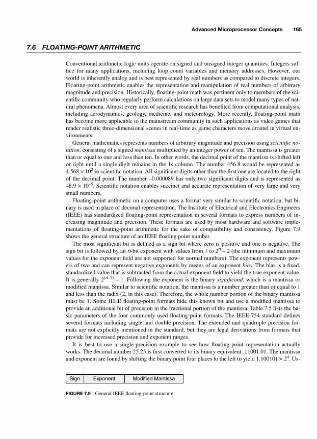
Advanced Microprocessor Concepts 165
7.6 FLOATING-POINT ARITHMETIC
Conventional arithmetic logic units operate on signed and unsigned integer quantities. Integers suf-fice for many applications, including loop count variables and memory addresses. However, ourworld is inherently analog and is best represented by real numbers as compared to discrete integers.Floating-point arithmetic enables the representation and manipulation of real numbers of arbitrarymagnitude and precision. Historically, floating-point math was pertinent only to members of the sci-entific community who regularly perform calculations on large data sets to model many types of nat-ural phenomena. Almost every area of scientific research has benefited from computational analysis,including aerodynamics, geology, medicine, and meteorology. More recently, floating-point mathhas become more applicable to the mainstream community in such applications as video games thatrender realistic three-dimensional scenes in real-time as game characters move around in virtual en-vironments.
General mathematics represents numbers of arbitrary magnitude and precision using scientific no-tation, consisting of a signed mantissa multiplied by an integer power of ten. The mantissa is greaterthan or equal to one and less than ten. In other words, the decimal point of the mantissa is shifted leftor right until a single digit remains in the 1s column. The number 456.8 would be represented as4.568 × 102 in scientific notation. All significant digits other than the first one are located to the rightof the decimal point. The number –0.000089 has only two significant digits and is represented as–8.9 × 10⁻⁵. Scientific notation enables succinct and accurate representation of very large and verysmall numbers.
Floating-point arithmetic on a computer uses a format very similar to scientific notation, but bi-nary is used in place of decimal representation. The Institute of Electrical and Electronics Engineers(IEEE) has standardized floating-point representation in several formats to express numbers of in-creasing magnitude and precision. These formats are used by most hardware and software imple-mentations of floating-point arithmetic for the sake of compatibility and consistency. Figure 7.9shows the general structure of an IEEE floating point number.
The most significant bit is defined as a sign bit where zero is positive and one is negative. Thesign bit is followed by an n-bit exponent with values from 1 to 2n – 2 (the minimum and maximumvalues for the exponent field are not supported for normal numbers). The exponent represents pow-ers of two and can represent negative exponents by means of an exponent bias. The bias is a fixed,standardized value that is subtracted from the actual exponent field to yield the true exponent value.It is generally 2(n–1) – 1. Following the exponent is the binary significand, which is a mantissa ormodified mantissa. Similar to scientific notation, the mantissa is a number greater than or equal to 1and less than the radix (2, in this case). Therefore, the whole number portion of the binary mantissamust be 1. Some IEEE floating-point formats hide this known bit and use a modified mantissa toprovide an additional bit of precision in the fractional portion of the mantissa. Table 7.5 lists the ba-sic parameters of the four commonly used floating-point formats. The IEEE-754 standard definesseveral formats including single and double precision. The extended and quadruple precision for-mats are not explicitly mentioned in the standard, but they are legal derivations from formats thatprovide for increased precision and exponent ranges.
It is best to use a single-precision example to see how floating-point representation actuallyworks. The decimal number 25.25 is first converted to its binary equivalent: 11001.01. The mantissaand exponent are found by shifting the binary point four places to the left to yield 1.100101 × 24. Us-
Sign Exponent Modified Mantissa
FIGURE 7.9 General IEEE floating-point structure.
-Balch.book Page 165 Thursday, May 15, 2003 3:46 PM
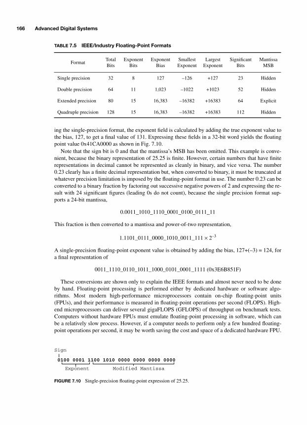
166 Advanced Digital Systems
ing the single-precision format, the exponent field is calculated by adding the true exponent value tothe bias, 127, to get a final value of 131. Expressing these fields in a 32-bit word yields the floatingpoint value 0x41CA0000 as shown in Fig. 7.10.
Note that the sign bit is 0 and that the mantissa’s MSB has been omitted. This example is conve-nient, because the binary representation of 25.25 is finite. However, certain numbers that have finiterepresentations in decimal cannot be represented as cleanly in binary, and vice versa. The number0.23 clearly has a finite decimal representation but, when converted to binary, it must be truncated atwhatever precision limitation is imposed by the floating-point format in use. The number 0.23 can beconverted to a binary fraction by factoring out successive negative powers of 2 and expressing the re-sult with 24 significant figures (leading 0s do not count), because the single precision format sup-ports a 24-bit mantissa,
0.0011_1010_1110_0001_0100_0111_11
This fraction is then converted to a mantissa and power-of-two representation,
1.1101_0111_0000_1010_0011_111 × 2–3
A single-precision floating-point exponent value is obtained by adding the bias, 127+(–3) = 124, fora final representation of
0011_1110_0110_1011_1000_0101_0001_1111 (0x3E6B851F)
These conversions are shown only to explain the IEEE formats and almost never need to be doneby hand. Floating-point processing is performed either by dedicated hardware or software algo-rithms. Most modern high-performance microprocessors contain on-chip floating-point units(FPUs), and their performance is measured in floating-point operations per second (FLOPS). High-end microprocessors can deliver several gigaFLOPS (GFLOPS) of throughput on benchmark tests.Computers without hardware FPUs must emulate floating-point processing in software, which canbe a relatively slow process. However, if a computer needs to perform only a few hundred floating-point operations per second, it may be worth saving the cost and space of a dedicated hardware FPU.
TABLE 7.5 IEEE/Industry Floating-Point Formats
FormatTotal Bits
Exponent Bits
Exponent Bias
Smallest Exponent
Largest Exponent
Significant Bits
Mantissa MSB
Single precision 32 8 127 –126 +127 23 Hidden
Double precision 64 11 1,023 –1022 +1023 52 Hidden
Extended precision 80 15 16,383 –16382 +16383 64 Explicit
Quadruple precision 128 15 16,383 –16382 +16383 112 Hidden
0100 0001 1100 1010 0000 0000 0000 0000
Exponent Modified Mantissa
Sign
FIGURE 7.10 Single-precision floating-point expression of 25.25.
-Balch.book Page 166 Thursday, May 15, 2003 3:46 PM

Advanced Microprocessor Concepts 167
As can be readily observed from Table 7.5, very large and very small numbers can be representedbecause of the wide ranges of exponents provided in the various formats. However, the representa-tion of 0 seems rather elusive with the requirement that the mantissa always have a leading 1. Valuesincluding 0 and infinity are represented by using the two-exponent values that are not supported fornormal numbers: 0 and 2n – 1. In the case of the single-precision format, these values are 0x00 and0xFF.
An exponent field of 0x00 is used to represent numbers of very small magnitude, where the inter-preted exponent value is fixed at the minimum for that format: –126 for single precision. With a 0exponent field, the mantissa’s definition changes to a number greater than or equal to 0 and less than1. Smaller numbers can now be represented, though with decreasing significant figures, becausemagnitude is now partially represented by the significand field. For example, 101 × 2–130 is ex-pressed as 0.0101 × 2–126. Such special-case numbers are denormalized, because their mantissasdefy the normalized form of being greater than or equal to 1 and less than 2. Zero can now be ex-pressed by setting the significand to 0 with the result that 0 × 2–126 = 0. The presence of the sign bitproduces two representations of zero, positive and negative, that are mathematically identical.
Setting the exponent field to 0xFF (in single precision) is used to represent either infinity or anundefined value. Positive and negative infinity are represented by setting the significand field to 0and using the appropriate sign bit. When the exponent field is 0xFF and the significand field is non-zero, the representation is “not a number,” or NaN. Examples of computations that may return NaNare 0 ÷ 0 and ∞ ÷ ∞.
7.7 DIGITAL SIGNAL PROCESSORS
Microprocessor architectures can be optimized for increased efficiency in certain applicationsthrough the inclusion of special instructions and execution units. One major class of application-spe-cific microprocessors is the digital signal processor, or DSP. DSP entails a microprocessor mathe-matically manipulating a sampled analog signal in a way that emulates transformation of that signalby discrete analog components such as filters or amplifiers. To operate on an analog signal digitally,the analog signal must be sampled by an analog-to-digital converter, manipulated, and then recon-structed with a digital-to-analog converter. A rough equivalency of digital signal processing versusconventional analog transformation is shown in Fig. 7.11 in the context of a simple filter.
Analog Filter
AnalogInput Signal
AnalogOutput Signal
Analog toDigital
ConverterDSP
Digital toAnalog
Converter
DigitalSamples
DigitalSamples
AnalogInput Signal
AnalogOutput Signal
FIGURE 7.11 Digital signal processing.
-Balch.book Page 167 Thursday, May 15, 2003 3:46 PM

168 Advanced Digital Systems
In this example of a lowpass filter (the amplitude of frequencies above a certain threshold are at-tenuated), the complexity of digital sampling and a microprocessor appears unjustified. The powerof DSP comes when much more complex analog transformations are performed that would requireexcessively complex analog circuit topologies. Some examples of applications in which DSPs areused include modems, cellular telephones, and radar. While sensitive analog circuits may degrade orfall out of calibration over time, digital instructions and sequences maintain their integrity indefi-nitely. Major manufacturers of DSPs include Analog Devices, Motorola, and Texas Instruments.Many books have been written on DSP algorithms and techniques, which are extremely diverse andchallenging topics.
DSP algorithms are characterized by repetitive multiplication and addition operations carried outon the sampled data set. Multiply and addition operations are also known as multiply and accumu-late, or MAC, operations in DSP parlance. These calculations involve the sampled data as well ascoefficients that, along with the specific operations, define the transformation being performed. ForDSP to be practical, it must be performed in real time, because the signals cannot be paused whilewaiting for the microprocessor to finish its previous operation. For DSP to be economical, thisthroughput must be achieved at an acceptable cost. A general-purpose microprocessor can be used toperform DSP functions, but in most cases, the solution will not be economical. This is because themicroprocessor is designed to execute general programs for which there is less emphasis on specifictypes of calculations. A DSP is designed specifically to rapidly execute multiply and accumulate op-erations, and it contains additional hardware to efficiently fetch sequential operands from tables inmemory. Not all of the features discussed below are implemented by all DSPs, but they are pre-sented to provide an understanding of the overall set of characteristics that differentiates a DSP froma generic microprocessor.
At their core, DSPs contain one or more ALUs that are capable of multiplication and addition in asingle cycle. This rapid calculation capability ensures that throughput can be maintained as long asoperands are fed to the ALUs. DSPs are manufactured with a variety of ALU capabilities rangingfrom 16-bit integer to IEEE floating-point support. As with a generic microprocessor, the number ofALUs influences how many simultaneous operations can be carried out at a given time. To keep theALUs supplied with operands, DSPs contain hardware structures called address generators that au-tomatically calculate the addresses of the next operands to be used in a calculation. Sampled data isstored in a memory array, and algorithmic coefficients are stored in a separate array. Depending onthe algorithm, the array entries may not be accessed sequentially. On a generic microprocessor, thesoftware would have to add an arbitrary offset value to an index register each time a new operandwas desired. Additionally, as a result of fixed array sizes, the pointer eventually wraps around fromthe end to the beginning, thereby requiring additional instructions to check for the wrap condition.This index register overhead slows the computation process. Address generators offload this over-head to hardware by associating additional registers with the index registers. These registers definethe increment to be applied to an index register following a load or store operation and also definethe start and end addresses of the memory array. Therefore, software is able to execute load/storeand calculation operations without spending time on routine pointer arithmetic.
The specialized ALU and address generation hardware within the DSP core place a high demandon memory to maintain a steady flow of instructions and data. DSPs commonly implement a Har-vard memory architecture in which separate buses connect to program and data memory. Most DSPscontain separate program and data memory structures integrated onto the same chip as the DSP corefor minimal access latency to small repetitive DSP algorithm kernels. Program memory may be im-plemented as ROM or RAM, depending on whether an external interface is available from which toload programs. These on-chip memories may be as small as several kilobytes each for less expensiveDSPs or hundreds of kilobytes for more powerful products. To mitigate the complexity of a Harvardarchitecture on the overall system design, most DSPs contain a unified external memory bus for con-
-Balch.book Page 168 Thursday, May 15, 2003 3:46 PM
Advanced Microprocessor Concepts 169
nection to external ROM and RAM. A DSP application can boot from external ROM, then load itskernel into on-chip program memory and perform the majority of its execution without fetching ad-ditional instructions from external memory.
7.8 PERFORMANCE METRICS
Evaluating the throughput potential of a microprocessor or a complete computer is not as simple asfinding out how fast the microprocessor’s clock runs. System performance varies widely accordingto the applications being used and the computing hardware on which they run. Applications varywidely in their memory and I/O usage, both being properties whose performance is directly tied tothe hardware architecture. We can consider three general sections of a computer and how each influ-ences the speed at which an application is executed: the microprocessor, the memory system, and theI/O resources.
The usable address space of a microprocessor is an important consideration, because applicationsvary in their memory needs. Some embedded applications can fit into several kilobytes of memory,making an 8-bit computer with 64 kB or less of address space quite adequate. More complex embed-ded applications start to look like applications that run on desktop computers. If large data arrays arecalled for, or if a multitasking system is envisioned whereby multiple tasks each contain megabytesof program memory and high-level data structures, a 32-bit microprocessor with hundreds of mega-bytes of usable address space may be necessary. At the very high end, microprocessors have transi-tioned to 64-bit architectures with gigabytes of directly addressable memory. A microprocessor’saddress space can always be expanded externally by banking methods, but banking comes at a pen-alty of increased time to switch banks and the complexity of making an application aware of thebanking scheme.
Any basic type of application can run on almost any microprocessor. The question is how fast andefficiently a particular microprocessor is able to handle the application. The instruction set is an im-portant attribute that should be considered when designing a computer system. If a floating-point in-tensive application is envisioned, it should probably be run on a microprocessor that contains anFPU, and the number of floating-point execution units and their execution latencies is an importantattribute to investigate. An integer-only microprocessor could most likely run the floating-point ap-plication by performing software emulation of floating-point operations, but its performance wouldprobably be rather dismal. For smaller-scale computers and applications, these types of questions arestill valid. If an application needs to perform frequent bit manipulations for testing and setting vari-ous flags, a microprocessor that directly supports bit manipulation may be better suited than a ge-neric architecture with only logical AND/OR type instructions.
Once a suitable instruction set has been identified, a microprocessor’s ability to actually fetch andexecute the instructions can become an important part of system performance. On smaller systems,there are few variables in instruction fetch and execution: each instruction is fetched and executedsequentially. Superscalar microprocessors, however, must include effective instruction analysis logicto properly utilize all the extra logic that has been put onto the chip and that you are paying for. If themultiple execution units cannot be kept busy enough of the time, your application will not enjoy thebenchmark performance claims of the manufacturer. Vendors of high-performance microprocessorsdevote much time to instruction profiling and analysis of instruction sequences. Their results im-prove performance on most applications, but there are always a few niche applications that have un-common properties that can cause certain microprocessors to fall off in performance. It pays to keepin mind that common industry benchmarks of microprocessor performance do not always tell thewhole story. These tests have been around for a long time, and microprocessor designers have
-Balch.book Page 169 Thursday, May 15, 2003 3:46 PM
170 Advanced Digital Systems
learned how to optimize their hardware to perform well on the standard benchmarks. An applicationthat behaves substantially differently from a benchmark test may not show the same level of perfor-mance as advertised by the manufacturer.
The microprocessor’s memory interface is a critical contributor to its performance. Whether asmall 8-bit microprocessor or a 64-bit behemoth, the speed with which instructions can be fetchedand data can be loaded and stored affects the execution time of an application. The necessary band-width of a memory interface is relative and is proportional to the sum of the instruction and databandwidths of an application. From the instruction perspective, it is clear that the microprocessorneeds to keep itself busy with a steady stream of instructions. Data bandwidth, however, is verymuch a function of the application. Some applications may perform frequent load/store operations,whereas others may operate more on data retained within the microprocessor’s register set. To theextent that load/store operations detract from the microprocessor’s ability to fetch and execute newinstructions, they will reduce overall throughput.
Clock frequency becomes a defining attribute of a microprocessor once its instruction set, exe-cution capabilities, and memory interface are understood from a performance perspective. Withoutthese supporting attributes, clock speed alone does not define the capabilities of a microprocessor.A 500-MHz single-issue, or nonsuperscalar, microprocessor could be easily outperformed by a200-MHz four-issue superscalar design. Additionally, there may be multiple relevant clocks to con-sider in a complex microprocessor. Microprocessors whose internal processing cores are decoupledfrom the external memory bus by an integrated cache are often specified with at least two clocks:the core clock and the bus interface clock. It is necessary to understand the effect of both clocks onthe processing core’s throughput. A fast core can be potentially starved for instructions and data bya slow interface. Once a microprocessor’s resources have been quantified, clock frequency be-comes a multiplier to determine how many useful operations per second can be expected. Metricssuch as instructions per second (IPS) or floating-point operations per second (FLOPS) are specifiedby multiplying the average number of instructions executed per cycle by how many cycles occureach second. Whereas high-end microprocessors were once measured in MIPS and MFLOPS,GIPS and GFLOPS performance levels are now attainable.
As already mentioned, memory bandwidth and, consequently, memory architecture hold keyroles in determining overall system performance. Memory system architecture encompasses allmemory external to the microprocessor’s core, including any integrated caches that it may contain.When dealing with an older-style microprocessor with a memory interface that does not stress cur-rent memory technologies, memory architecture may not be subject to much variability and may notbe a bottleneck at all. It is not hard to find flash, EPROM, and SRAM devices today with accesstimes of 50 ns and under. A moderately sized memory array constructed from these componentscould provide an embedded microprocessor with full-speed random access as long as the memorytransaction rate is 20 MHz or less. Many 8-, 16-, and even some 32-bit embedded microprocessorscan fit comfortably within this performance window. As such, computers based on these devices canhave simple memory architectures without suffering performance degradation.
Memory architecture starts to get more complicated when higher levels of performance are de-sired. Once the microprocessor’s program and data fetch latency becomes faster than main mem-ory’s random access latency, caching and bandwidth improvement techniques become critical tosustaining system throughput. Random access latency is the main concern. A large memory arraycan be made to deliver adequate bandwidth given a sufficient width. As a result of the limited operat-ing frequency of SDRAM devices, high-end workstation computers have been known to connectmultiple memory chips in parallel to create 256-bit and even 512-bit wide interfaces. Using 512 MbDDR SDRAMs, each organized as 32M × 16 and running at 167 MHz, 16 devices in parallel wouldyield a 1-GB memory array with a burst bandwidth of 167 MHz × 2 words/hertz × 256 bits/word =85.5 Gbps! This is a lot of bandwidth, but relative to a microprocessor core that operates at 1 GHz or
-Balch.book Page 170 Thursday, May 15, 2003 3:46 PM

Advanced Microprocessor Concepts 171
more with a 32- or 64-bit data path, such a seemingly powerful memory array may just barely beable to keep up.
While bandwidth can be increased by widening the interface, random access latency does not goaway. Therefore, there is more to a memory array than its raw size. The bandwidth of the array,which is the product of its interface frequency and width, and its latency are important metrics in un-derstanding the impact of cache misses, especially when dealing with applications that exhibit poorlocality.
Caching reduces the negative effect of high random access latencies on a microprocessor’sthroughput. However, caches and wide arrays cannot completely balance the inequality between thebandwidth and latency that the microprocessor demands and that which is provided by SDRAM tech-nology. Cache size, type, and latency and main memory bandwidth are therefore important metricsthat contribute to overall system performance. An application’s memory characteristics determinehow costly a memory architecture is necessary to maintain adequate performance. Applications thatoperate on smaller sets of data with higher degrees of locality will be less reliant on a large cache andfast memory array, because they will have fewer cache misses. Those applications with oppositememory characteristics will increase the memory architecture’s effect on the computer’s overall per-formance. In fact, by the nature of the application being run, caching effects can become more signif-icant than the microprocessor’s core clock frequency. In some situations, a 500-MHz microprocessorwith a 2-MB cache can outperform a 1-GHz microprocessor with a 256-kB cache. It is important tounderstand these considerations because money may be better spent on either a faster microprocessoror a larger cache according to the needs of the intended applications.
I/O performance affects system throughput in two ways: the latency of executing transactions andthe degree to which such execution blocks the microprocessor from performing other work. In acomputer in which the microprocessor operates with a substantially higher bandwidth than individ-ual I/O interfaces, it is desirable to decouple the microprocessor from the slower interface as muchas possible. Most I/O controllers provide a natural degree of decoupling. A typical UART, for exam-ple, absorbs one or more bytes in rapid succession from a microprocessor and then transmits them ata slower serial rate. Likewise, the UART assembles one or more whole incoming bytes that the mi-croprocessor can read at an instantaneous bandwidth much higher than the serial rate. Network anddisk adapters often contain buffers of several kilobytes that can be rapidly filled or drained by themicroprocessor. The microprocessor can then continue with program execution while the adapterlogic handles the data at whatever lower bandwidth is inherent to the physical interface.
Inherent decoupling provided by an I/O controller is sufficient for many applications. When deal-ing with very I/O-intensive applications, such as a large server, multiple I/O controllers may interactwith each other and memory simultaneously in a multimaster bus configuration. In such a context,the microprocessor sets up block data transfers by programming multiple I/O and DMA controllersand then resumes work processing other tasks. Each I/O and DMA controller is a potential bus mas-ter that can arbitrate for access to the memory system and the I/O bus (if there is a separate I/O bus).As the number of simultaneous bus masters increases, contention can develop, which may cause per-formance degradation resulting from excessive waiting time by each potential bus master. This con-tention can be reduced by modifying the I/O bus architecture. A first step is to decouple the I/O busfrom the memory bus into one or more segments, enabling data transfers within a given I/O segmentto proceed without conflicting with a memory transfer or one contained within other I/O segments.PCI is an example of such a solution. At a more advanced level, the I/O system can be turned into aswitched network in which individual I/O controllers or small segments of I/O controllers are con-nected to a dedicated port on an I/O switch that enables each port to communicate with any otherport simultaneously insofar as multiple ports do not conflict for access to the same port. This is afairly expensive solution that is implemented in high-end servers for which I/O performance is a keycontributor to overall system throughput.
-Balch.book Page 171 Thursday, May 15, 2003 3:46 PM

172 Advanced Digital Systems
The question of how fast a computer performs does not depend solely on how many megahertzthe microprocessor runs at or how much RAM it has. Performance is highly application specific andis dominated by how many cycles per second the microprocessor is kept busy with useful instruc-tions and data.
-Balch.book Page 172 Thursday, May 15, 2003 3:46 PM

173
CHAPTER 8
High-Performance Memory Technologies
Memory is an interesting and potentially challenging portion of a digital system design. One of thebenefits of decades of commercial solid-state memory development is the great variety of memoryproducts available for use. Chances are that there is an off-the-shelf memory product that fits yourspecific application. A downside to the modern, ever-changing memory market is rapid obsolescenceof certain products. DRAM is tied closely to the personal computer market. The best DRAM valuesare those devices that coincide with the sweet spot in PC memory configurations. As the high-vol-ume PC market moves on to higher-density memory ICs, that convenient DRAM that you used inyour designs several years ago may be discontinued so that the manufacturer can retool the factoryfor parts that are in greater demand.
Rapid product development means that memory capabilities improve dramatically each year.Whether it’s higher density or lower power that an application demands, steady advances in technol-ogy put more tools at an engineer’s disposal. SRAM and flash EPROM devices have more stableproduction lives than DRAM. In part, this is because they are less dependent on the PC market,which requires ever increasing memory resources for ever more complex software applications.
Memory is a basic digital building block that is used for much more than storing programs anddata for a microprocessor. Temporary holding buffers are used to store data as it is transferred fromone interface to another. There are many situations in networking and communication systems wherea block of data arrives and must be briefly stored in a buffer until the logic can figure out exactlywhat to do with it. Lookup tables are another common use for memory. A table may store precom-puted terms of a complex calculation so that a result can be rapidly determined when necessary. Thischapter discusses the predominant synchronous memory technologies, SDRAM and SSRAM, andcloses with a presentation of CAM, a technology that is part RAM and part logic.
No book can serve as an up-to-date reference on memory technology for long, as a result of theindustry’s rapid pace. This chapter discusses technologies and concepts that are timeless, but specif-ics of densities, speeds, and interface protocols change rapidly. Once you have read and understoodthe basics of high-performance memory technologies, you are encouraged to browse through the lat-est manufacturers’ data sheets to familiarize yourself with the current state of the art. Corporationssuch as Cypress, Hynix, Infineon, Micron, NEC, Samsung, and Toshiba provide detailed data sheetson their web sites that are extremely useful for self-education and selecting the right memory deviceto suit your needs.
8.1 SYNCHRONOUS DRAM
As system clock frequencies increased well beyond 50 MHz, conventional DRAM devices withasynchronous interfaces became more of a limiting factor in overall system performance. Asynchro-
-Balch.book Page 173 Thursday, May 15, 2003 3:46 PM
Copyright 2003 by The McGraw-Hill Companies, Inc. Click Here for Terms of Use.
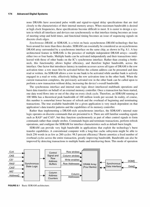
174 Advanced Digital Systems
nous DRAMs have associated pulse width and signal-to-signal delay specifications that are tiedclosely to the characteristics of their internal memory arrays. When maximum bandwidth is desiredat high clock frequencies, these specifications become difficult to meet. It is easier to design a sys-tem in which all interfaces and devices run synchronously so that interface timing becomes an issueof meeting setup and hold times, and functional timing becomes an issue of sequencing signals ondiscrete clock edges.
Synchronous DRAM
, or SDRAM, is a twist on basic asynchronous DRAM technology that hasbeen around for more than three decades. SDRAM can essentially be considered as an asynchronousDRAM array surrounded by a synchronous interface on the same chip, as shown in Fig. 8.1. A keyarchitectural feature in SDRAMs is the presence of multiple independent DRAM arrays—usuallyeither two or four banks. Multiple banks can be activated independently and their transactions inter-leaved with those of other banks on the IC’s synchronous interface. Rather than creating a bottle-neck, this functionality allows higher efficiency, and therefore higher bandwidth, across theinterface. One factor that introduces latency in random accesses across all types of DRAM is the rowactivation time: a row must first be activated before the column address can be presented and dataread or written. An SDRAM allows a row in one bank to be activated while another bank is activelyengaged in a read or write, effectively hiding the row activation time in the other bank. When thecurrent transaction completes, the previously activated row in the other bank can be called upon toperform a new transaction without delay, increasing the device’s overall bandwidth.
The synchronous interface and internal state logic direct interleaved multibank operations andburst data transfers on behalf of an external memory controller. Once a transaction has been started,one data word flows into or out of the chip on every clock cycle. Therefore, an SDRAM running at100 MHz has a theoretical peak bandwidth of 100 million words per second. In reality, of course,this number is somewhat lower because of refresh and the overhead of beginning and terminatingtransactions. The true available bandwidth for a given application is very much dependent on thatapplication’s data transfer patterns and the capabilities of its memory controller.
Rather than implementing a DRAM-style asynchronous interface, the SDRAM’s internal statelogic operates on discrete commands that are presented to it. There are still familiar sounding signalssuch as RAS* and CAS*, but they function synchronously as part of other control signals to formcommands rather than simple strobes. Commands begin and terminate transactions, perform refreshoperations, and configure the SDRAM for interface characteristics such as default burst length.
SDRAM can provide very high bandwidth in applications that exploit the technology’s bursttransfer capabilities. A conventional computer with a long-line cache subsystem might be able tofetch 256 words in as few as 260 cycles: 98.5 percent efficiency! Bursts amortize a fixed number ofoverhead cycles across the entire transaction, greatly improving bandwidth. Bandwidth can also beimproved by detecting transactions to multiple banks and interleaving them. This mode of operation
ColumnAddressCounters
ControlSignal and
RowAddressBuffers
DRAM Array(Four
Banks)
DRAM Array(Four
Banks)
DRAM Array(Four
Banks)
DRAM Array(Four Banks)
Row strobes
Column strobes
Write enables
Row Addresses
ColumnAddresses
SynchronousState Logic
SynchronousData Interface
DQM[]
Data[]
CLK
CKE
CS*
RAS*
CAS*
WE*
Address[]
FIGURE 8.1 Basic SDRAM architecture.
-Balch.book Page 174 Thursday, May 15, 2003 3:46 PM

High-Performance Memory Technologies 175
allows some new burst transfers to be requested prior to the current burst ending, thereby hiding theinitial startup latency of the subsequent transaction.
Most of the input signals to the state logic shown in Fig. 8.1 combine to form the discrete com-mands listed in Table 8.1. A clock enable, CKE, must be high for normal operation. When CKE islow, the SDRAM enters a low-power mode during which data transactions are not recognized. CKEcan be tied to logic 1 for applications that are either insensitive to power savings or require continualaccess to the SDRAM. Interface signals are sampled on the rising clock edge. Many SDRAM de-vices are manufactured in multibyte data bus widths. The data mask signals, DQM[], provide a con-venient way to selectively mask individual bytes from being written or being driven during reads.Each byte lane has an associated DQM signal, which must be low for the lane to be written or to en-able the lane’s tri-state buffers on a read.
Some common functions include activating a row for future access, performing a read, and pre-charging a row (deactivating a row, often in preparation for activating a new row). For complete de-scriptions of SDRAM interface signals and operational characteristics, SDRAM manufacturers’ datasheets should be referenced directly. Figure 8.2 provides an example of how these signals are used toimplement a transaction and serves as a useful vehicle for introducing the synchronous interface.CS* and CKE are assumed to be tied low and high, respectively, and are not shown for clarity.
The first requirement to read from an SDRAM is to activate the desired row in the desired bank.This is done by asserting an activate (ACTV) command, which is performed by asserting RAS* forone cycle while presenting the desired bank and row addresses. The next command issued to con-tinue the transaction is a read (RD). However, the controller must wait a number of cycles that trans-lates into the DRAM array’s row-activate to column-strobe delay time. The timing characteristics ofthe underlying DRAM array is expressed in nanoseconds rather than clock cycles. Therefore, the in-teger number of delay cycles is different for each design, because it is a function of the clock periodand the internal timing specification. If, for example, an SDRAM’s RAS* to CAS* delay is 20 ns,and the clock period is 20 ns or slower, an RD command could be issued on the cycle immediately
TABLE
8.1 Basic SDRAM Command Set
Command CS* RAS* CAS* WE* Address AP/A10
Bank activate L L H H Bank, row A10
Read L H L H Bank, column L
Read with auto-precharge L H L H Bank, column H
Write L H L L Bank, column L
Write with auto-precharge L H L L Bank, column H
No operation L H H H X X
Burst terminate L H H L X X
Bank precharge L L H L X L
Precharge all banks L L H L X H
Mode register set L L L L Configuration Configuration
Auto refresh L L L H X X
Device deselect H X X X X X
-Balch.book Page 175 Thursday, May 15, 2003 3:46 PM
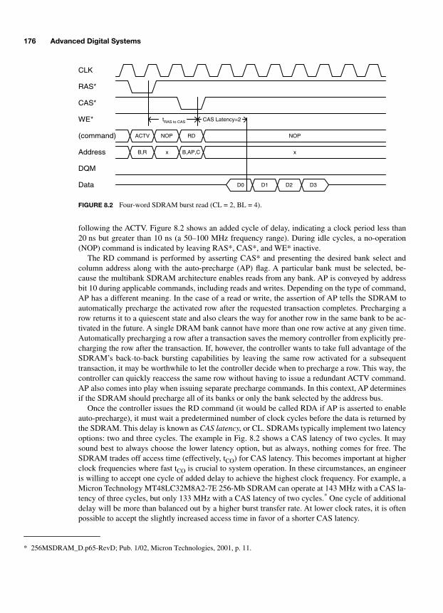
176 Advanced Digital Systems
following the ACTV. Figure 8.2 shows an added cycle of delay, indicating a clock period less than20 ns but greater than 10 ns (a 50–100 MHz frequency range). During idle cycles, a no-operation(NOP) command is indicated by leaving RAS*, CAS*, and WE* inactive.
The RD command is performed by asserting CAS* and presenting the desired bank select andcolumn address along with the auto-precharge (AP) flag. A particular bank must be selected, be-cause the multibank SDRAM architecture enables reads from any bank. AP is conveyed by addressbit 10 during applicable commands, including reads and writes. Depending on the type of command,AP has a different meaning. In the case of a read or write, the assertion of AP tells the SDRAM toautomatically precharge the activated row after the requested transaction completes. Precharging arow returns it to a quiescent state and also clears the way for another row in the same bank to be ac-tivated in the future. A single DRAM bank cannot have more than one row active at any given time.Automatically precharging a row after a transaction saves the memory controller from explicitly pre-charging the row after the transaction. If, however, the controller wants to take full advantage of theSDRAM’s back-to-back bursting capabilities by leaving the same row activated for a subsequenttransaction, it may be worthwhile to let the controller decide when to precharge a row. This way, thecontroller can quickly reaccess the same row without having to issue a redundant ACTV command.AP also comes into play when issuing separate precharge commands. In this context, AP determinesif the SDRAM should precharge all of its banks or only the bank selected by the address bus.
Once the controller issues the RD command (it would be called RDA if AP is asserted to enableauto-precharge), it must wait a predetermined number of clock cycles before the data is returned bythe SDRAM. This delay is known as
CAS latency
, or CL. SDRAMs typically implement two latencyoptions: two and three cycles. The example in Fig. 8.2 shows a CAS latency of two cycles. It maysound best to always choose the lower latency option, but as always, nothing comes for free. TheSDRAM trades off access time (effectively, t
CO
) for CAS latency. This becomes important at higherclock frequencies where fast t
CO
is crucial to system operation. In these circumstances, an engineeris willing to accept one cycle of added delay to achieve the highest clock frequency. For example, aMicron Technology MT48LC32M8A2-7E 256-Mb SDRAM can operate at 143 MHz with a CAS la-tency of three cycles, but only 133 MHz with a CAS latency of two cycles.
*
One cycle of additionaldelay will be more than balanced out by a higher burst transfer rate. At lower clock rates, it is oftenpossible to accept the slightly increased access time in favor of a shorter CAS latency.
* 256MSDRAM_D.p65-RevD; Pub. 1/02, Micron Technologies, 2001, p. 11.
Address
DQM
CAS*
WE*
RAS*
(command)
CLK
Data
ACTV NOP RD NOP
B,R x B,AP,C x
D0 D1 D2 D3
tRAS to CAS CAS Latency=2
FIGURE 8.2 Four-word SDRAM burst read (CL = 2, BL = 4).
-Balch.book Page 176 Thursday, May 15, 2003 3:46 PM

High-Performance Memory Technologies 177
Once the CAS latency has passed, data begins to flow on every clock cycle. Data will flow for aslong as the specified burst length. In Fig. 8.2, the standard burst length is four words. This parameteris configurable and adds to the flexibility of an SDRAM. The controller is able to set certain param-eters at start-up, including CAS latency and burst length. The burst length then becomes the defaultunit of data transfer across an SDRAM interface. Longer transactions are built from multiple back-to-back bursts, and shorter transactions are achieved by terminating a burst before it has completed.SDRAMs enable the controller to configure the standard burst length as one, two, four, or eightwords, or the entire row. It is also possible to configure a long burst length for reads and only single-word writes. Configuration is performed with the mode register set (MRS) command by assertingthe three primary control signals and driving the desired configuration word onto the address bus.
As previously mentioned, DQM signals function as an output disable on a read. The DQM bus (asingle signal for SDRAMs with data widths of eight bits or less) follows the CAS* timing and,therefore, leads read data by the number of cycles defined in the CAS latency selection. The preced-ing read can be modified as shown in Fig. 8.3 to disable the two middle words.
In contrast, write data does not have an associated latency with respect to CAS*. Write data be-gins to flow on the same cycle that the WR/WRA command is asserted, as shown in Fig. 8.4. This
Address
DQM
CAS*
WE*
RAS*
(command)
CLK
Data
ACTV NOP RD NOP
B,R x B,AP,C x
D0 D1 D2 D3
FIGURE 8.3 Four-word SDRAM burst read with DQM disable (CL = 2, BL = 4).
CLK
Data
ACTV NOP WR NOP
B,R x B,AP,C x
D0 x x D3
FIGURE 8.4 Four-word SDRAM burst write with DQM masking (BL = 4).
-Balch.book Page 177 Thursday, May 15, 2003 3:46 PM
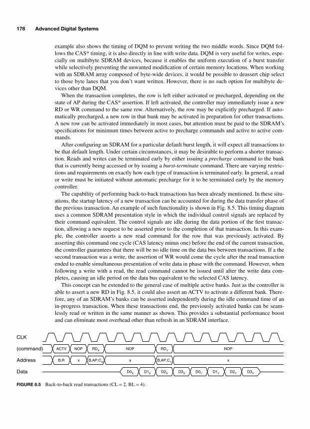
178 Advanced Digital Systems
example also shows the timing of DQM to prevent writing the two middle words. Since DQM fol-lows the CAS* timing, it is also directly in line with write data. DQM is very useful for writes, espe-cially on multibyte SDRAM devices, because it enables the uniform execution of a burst transferwhile selectively preventing the unwanted modification of certain memory locations. When workingwith an SDRAM array composed of byte-wide devices, it would be possible to deassert chip selectto those byte lanes that you don’t want written. However, there is no such option for multibyte de-vices other than DQM.
When the transaction completes, the row is left either activated or precharged, depending on thestate of AP during the CAS* assertion. If left activated, the controller may immediately issue a newRD or WR command to the same row. Alternatively, the row may be explicitly precharged. If auto-matically precharged, a new row in that bank may be activated in preparation for other transactions.A new row can be activated immediately in most cases, but attention must be paid to the SDRAM’sspecifications for minimum times between active to precharge commands and active to active com-mands.
After configuring an SDRAM for a particular default burst length, it will expect all transactions tobe that default length. Under certain circumstances, it may be desirable to perform a shorter transac-tion. Reads and writes can be terminated early by either issuing a
precharge
command to the bankthat is currently being accessed or by issuing a
burst-terminate
command. There are varying restric-tions and requirements on exactly how each type of transaction is terminated early. In general, a reador write must be initiated without automatic precharge for it to be terminated early by the memorycontroller.
The capability of performing back-to-back transactions has been already mentioned. In these situ-ations, the startup latency of a new transaction can be accounted for during the data transfer phase ofthe previous transaction. An example of such functionality is shown in Fig. 8.5. This timing diagramuses a common SDRAM presentation style in which the individual control signals are replaced bytheir command equivalent. The control signals are idle during the data portion of the first transac-tion, allowing a new request to be asserted prior to the completion of that transaction. In this exam-ple, the controller asserts a new read command for the row that was previously activated. Byasserting this command one cycle (CAS latency minus one) before the end of the current transaction,the controller guarantees that there will be no idle time on the data bus between transactions. If a thesecond transaction was a write, the assertion of WR would come the cycle after the read transactionended to enable simultaneous presentation of write data in phase with the command. However, whenfollowing a write with a read, the read command cannot be issued until after the write data com-pletes, causing an idle period on the data bus equivalent to the selected CAS latency.
This concept can be extended to the general case of multiple active banks. Just as the controller isable to assert a new RD in Fig. 8.5, it could also assert an ACTV to activate a different bank. There-fore, any of an SDRAM’s banks can be asserted independently during the idle command time of anin-progress transaction. When these transactions end, the previously activated banks can be seam-lessly read or written in the same manner as shown. This provides a substantial performance boostand can eliminate most overhead other than refresh in an SDRAM interface.
Address
(command)
CLK
Data
ACTV NOP RDX NOP
B,R x B,AP,CX x
D0X D1X D2X D3X
RDY
B,AP,CY
NOP
x
D1Y D2Y D3YD0Y
FIGURE 8.5 Back-to-back read transactions (CL = 2, BL = 4).
-Balch.book Page 178 Thursday, May 15, 2003 3:46 PM

High-Performance Memory Technologies 179
Periodic refresh is a universal requirement of DRAM technology, and SDRAMs are no exception.An SDRAM device may contain 4,096 rows per bank (or 8,192, depending on its overall size) withthe requirement that all rows be refreshed every 64 ms. Therefore, the controller has the responsibil-ity of ensuring that 4,096 (or 8,192) refresh operations are carried out every 64 ms. Refresh com-mands can be evenly spaced every 15.625 µs (or 7.8125 µs), or the controller might wait until acertain event has passed and then rapidly count out 4,096 (or 8,192) refresh commands. DifferentSDRAM devices have slightly differing refresh requirements, but the means of executing refresh op-erations is standardized. The first requirement is that all banks be precharged, because the auto-re-fresh (REF) command operates on all banks at once. An internal refresh counter keeps track of thenext row across each bank to be refreshed when a REF command is executed by asserting RAS* andCAS* together.
It can be easy to forget the asynchronous timing requirements of the DRAM core when designingaround an SDRAM’s synchronous interface. After a little time spent studying state transition tablesand command sets, the idea that an asynchronous element is lurking in the background can becomean elusive memory. Always be sure to verify that discrete clock cycle delays conform to the nanosec-ond timing specifications that are included in the SDRAM data sheet. The tricky part of these timingspecifications is that they affect a system differently, depending on the operating frequency. At25 MHz, a 20-ns time delay is less than one cycle. However, at 100 MHz, that delay stretches to twocycles. Failure to recognize subtle timing differences can cause errors that may manifest themselvesas intermittent data corruption problems, which can be very time consuming to track down.
SDRAM remains a mainstream memory technology for PCs and therefore is manufactured insubstantial volumes by multiple manufacturers. The SDRAM market is a highly competitive one,with faster and denser products appearing regularly. SDRAMs are commonly available in densitiesranging from 64 to 512 Mb in 4, 8, and 16-bit wide data buses. Older 16-Mb parts are becomingharder to find. For special applications, 32-bit wide devices are available, though sometimes at aslight premium as a result of lower overall volumes.
8.2 DOUBLE DATA RATE SDRAM
Conventional SDRAM devices transfer one word on the rising edge of each clock cycle. At anygiven time, there is an upper limit on the clock speed that is practical to implement for a board-levelinterface. When this level of performance proves insufficient,
double data rate
(DDR) SDRAM de-vices can nearly double the available bandwidth by transferring one word on both the rising and fall-ing edges of each clock cycle. In doing so, the interface’s clock speed remains constant, but the databus effectively doubles in frequency. Functionally, DDR and single data rate (SDR) devices are verysimilar. They share many common control signals, a common command set, and a rising-edge-onlycontrol/address interface. They differ not only in the speed of the data bus but also with new DDRdata control signals and internal clocking circuitry to enable reliable circuit design with very tighttiming margins. Figure 8.6 shows the DDR SDRAM structure.
A DDR SDRAM contains an internal data path that is twice the width of the external data bus.This width difference allows the majority of the internal logic to run at a slower SDR frequencywhile delivering the desired external bandwidth with half as many data pins as would be requiredwith a conventional SDRAM. Rather than supplying a 2
×
clock to the SDRAM for its DDR inter-face, a pair of complementary clocks, CLK and CLK*, are provided that are 180° out of phase witheach other. Input and output signals are referenced to the crossings of these two clocks, during whicha rising edge is always present in either clock. Commands and addresses are presented to a DDRSDRAM as they would be for an SDR device: on the rising edge of CLK. It is not necessary to dou-
-Balch.book Page 179 Thursday, May 15, 2003 3:46 PM

180 Advanced Digital Systems
ble the speed of the control interface, because an SDRAM is almost always used in burst modewhere the rate of commands is significantly less than the rate of data transferred.
The data interface contains a mask that has been renamed to DM and a new data strobe signal,DQS. DM functions as DQM does in an SDR device but operates at DDR to match the behavior ofdata. DQS is a bidirectional clock that is used to help time the data bus on both reads and writes. Onwrites, DQS, DM, and data are inputs and DQS serves as a clock that the SDRAM uses to sampleDM and data. Setup and hold times are specified relative to both the rising and falling edges of DQS,so DQS transitions in the middle of the data valid window. DQS and data are outputs for reads andare collectively timed relative to CLK/CLK*. DQS transitions at roughly the same time as data andso it transitions at the beginning of the data valid window.
When reading, 2n bits are fetched from the DRAM array on the CLK domain and are fed into a2:1 multiplexer that crosses the SDR/DDR clock domain. In combination with a DQS generator, themultiplexer is cycled at twice the CLK frequency to yield a double rate interface. This scheme is il-lustrated schematically in Fig. 8.7. Because DQS and data are specified relative to CLK/CLK* onreads, the memory controller can choose to clock its input circuitry with any of the strobe or clocksignals according to the relevant timing specifications. Writes function in a reverse scheme by stack-ing two n-bit words together to form a 2n-bit word in the DRAM’s CLK domain. Two registers areeach clocked alternately on the rising and falling edges of DQS, and their contents are then trans-ferred to a shallow write FIFO. A FIFO is necessary to cross from the DQS to CLK domains reliablyas a result of skew between the two signals.
Tight timing specifications characterize DDR SDRAM because of its high-speed operation: a333-MHz data rate with a 167-MHz clock is not an uncommon operating frequency. For reliable op-eration, careful planning must be done at the memory controller and in printed circuit board designto ensure that data is captured in as little as 1.5 ns (for a 333/167-MHz DDR SDRAM). These high-
SynchronousState Logic
2n-BitReadLatch
DQS
CLK*
CKE
CS*
RAS*
CAS*
WE*
Address[]
DRAM Array(Four
Banks)
DRAM Array(Four
Banks)
DRAM Array(Four
Banks)
DRAM Array(Four Banks)
CLK
2:1
DQS Generator
Data
DM
ShallowMask and
DataFIFO
Mask, DataInput Register
Mask, DataInput Register
SDR Domain
DDR Domain
FIGURE 8.6 Basic DDR SDRAM architecture.
DQS
CLK
Data DHI DLO DHI
DHI
DLO
1
0
DataRead Data
1
0
DQS"1"
"0"
CLK
FIGURE 8.7 SDR-to-DDR data conversion scheme.
-Balch.book Page 180 Thursday, May 15, 2003 3:46 PM

High-Performance Memory Technologies 181
speed data buses are treated as
source-synchronous
rather than synchronous. A source-synchronousbus is one where a local clock is generated along with data and routed on the circuit board with thedata signals. The clock and data signals are length-matched to a certain tolerance to greatly reducethe skew between all members of the bus. In doing so, the timing relationships between clock anddata are preserved almost exactly as they are generated by the sending device. A source-synchronousbus eliminates system-level skew problems that result from clocks and data signals emanating fromdifferent sources and taking different paths to their destinations. Treating the DDR SDRAM data bussource-synchronously as shown in Fig. 8.7 guarantees that the data valid window provided by thedriver will be available to the load. Likewise, because DQS is bidirectional, the SDRAM will obtainthe same timing benefit when accepting write-data from the memory controller.
Methods vary across DDR SDRAM implementations. While the SDRAM requires a fixed rela-tionship between DQS and data for writes, the memory controller may use either DQS or a source-synchronous version of CLK with which to time read data. DQS must be used for the fastest applica-tions, because it has a closer timing relationship relative to data. The usage of DQS adds some com-plexity, because it is essentially a bidirectional clock. There are also multiple DQS signals in mostapplications, because one DQS is present for every eight bits of data.
Some applications may be able to use CLK/CLK* to register read data. The memory controllertypically drives CLK/CLK* to the SDRAM along with address and control signals in a source-syn-chronous fashion. To achieve a source-synchronous read data bus, a skewed version of CLK/CLK*is necessary that is in phase with the returned data so that the memory controller sees timing asshown in Fig. 8.7. This skew is the propagation delay through the wires that carry the clocks fromthe memory controller to the SDRAM. These skews are illustrated in Fig. 8.8a, and the associatedwiring implementation is shown in Fig. 8.8b. CLK´ and CLK´* are the clocks that have been skewedby propagation delay through the wiring. A source-synchronous read-data bus is achieved by gener-ating a second pair of clocks that are identical to the main pair and then by matching their lengths tothe sum of the wire lengths to and from the SDRAM. The first length component cancels out thepropagation delay to the SDRAM, and the second length component maintains timing alignment, orphase, with the data bus.
With the exception of a faster data bus, a DDR SDRAM functions very much like a conventionalSDRAM. Commands are issued on the rising edge of CLK and are at a single data rate. Because ofthe internal 2n-bit architecture, a minimum burst size of two words is supported. The other burstlength options are four or eight words. To read or write a single word, DM must be used to mask orinhibit the applicable word. Two CAS latency options are supported for reads: 2 and 2.5 cycles. TwoCL = 2 reads are shown in Fig. 8.9. DQS transitions from input (tri-state) to output one cycle (1.5 cy-cles for CL = 2.5) after the assertion of the read command. It is driven low for one full cycle (twoDDR periods) and then transitions on each half of CLK for the duration of the burst, after which it
MemoryController
DDRSDRAM
CLK/CLK* (length=LC)
Data (length=LD)
CLK'/CLK'* (length=LC+LD)
(b)
CLK@MC
Data@RAM
CLK@RAM
Data@MC
CLK'@MC
(a)
FIGURE 8.8 Source-synchronous read data with CLK/CLK*.
-Balch.book Page 181 Thursday, May 15, 2003 3:46 PM

182 Advanced Digital Systems
returns to tri-state. Reads may be executed consecutively to achieve high bus utilization by hidingrow activation and CAS latency delays, as with an SDR SDRAM.
Unlike an SDR SDRAM, writes are subject to a brief latency between assertion of the write com-mand and delivery of write data. The first write data is presented on the first rising edge of DQS fol-lowing the write command. DQS is not driven to the SDRAM until just after the write command ispresented. This restriction prevents a collision between the SDRAM and the memory controllerwhen a write follows a read by giving time for the SDRAM to turn off its DQS driver. Following thewrite, DQS can remain driven until a read command is asserted, at which time the SDRAM willneed to drive the strobe. Write timing is shown in Fig. 8.10. Writes may also be executed consecu-tively to more effectively utilize the device interface.
When transitioning between reading and writing, minimum delays are introduced in a situationunlike that of a conventional SDRAM. Because write data lags the write command by a clock cycle,a cycle is lost when following a read with a write, because the write command cannot be issued untilthe read burst is complete (as with an SDR SDRAM). Going the other way, an explicit single-cycledelay is imposed on issuing a read command following a write burst, thereby incurring a data busidle time equal to the selected CAS latency plus the single cycle write/read delay.
DDR SDRAM has taken the place of conventional SDRAM in many PC applications. Like SDRSDRAM, DDR devices are commonly available in densities ranging from 64 to 512 Mb in 4-, 8-,and 16-bit wide data buses. Thirty-two-bit devices are also available, although they are not the sweetspot for the industry as a whole.
8.3 SYNCHRONOUS SRAM
Like DRAM, high-performance SRAM transitioned to a synchronous interface to gain performanceimprovements. Several basic types of
synchronous SRAM
(SSRAM) devices appeared and became
CLK
Data
ACTV NOP RDX
B,R x B,AP,CX
D0X D1X D2X D3X
DQS
NOP
x
RDY
B,AP,CY
D0Y D1Y D2Y D3Y
x
NOP
FIGURE 8.9 Consecutive DDR SDRAM reads (CL = 2, BL = 4).
Address
(command)
CLK
Data
ACTV NOP WRX
B,R x B,AP,CX
D0X D1X D2X D3X
DQS
NOP
x
WRY
B,AP,CY
D0Y D1Y D2Y D3Y
x
NOP
FIGURE 8.10 Consecutive DDR SDRAM writes (BL = 4).
-Balch.book Page 182 Thursday, May 15, 2003 3:46 PM
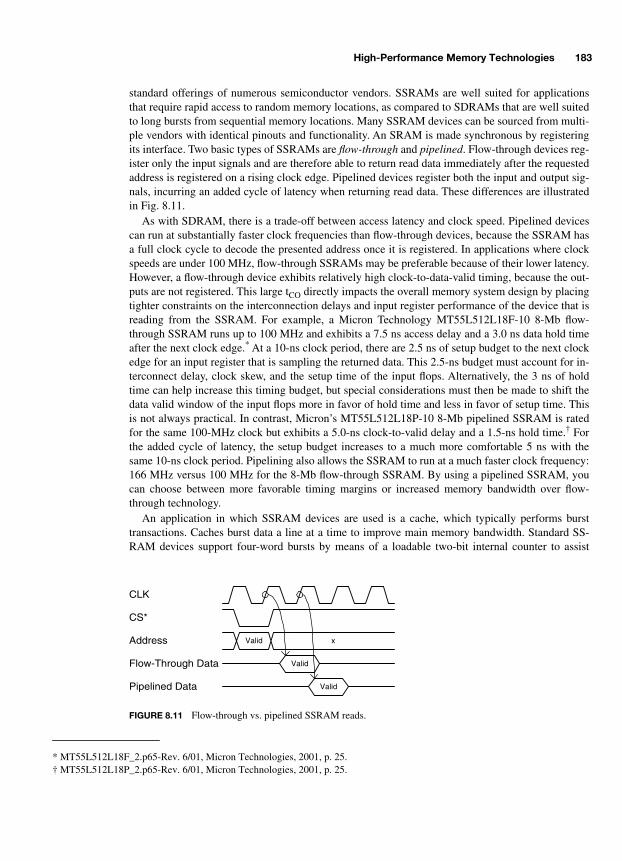
High-Performance Memory Technologies 183
standard offerings of numerous semiconductor vendors. SSRAMs are well suited for applicationsthat require rapid access to random memory locations, as compared to SDRAMs that are well suitedto long bursts from sequential memory locations. Many SSRAM devices can be sourced from multi-ple vendors with identical pinouts and functionality. An SRAM is made synchronous by registeringits interface. Two basic types of SSRAMs are
flow-through
and
pipelined
. Flow-through devices reg-ister only the input signals and are therefore able to return read data immediately after the requestedaddress is registered on a rising clock edge. Pipelined devices register both the input and output sig-nals, incurring an added cycle of latency when returning read data. These differences are illustratedin Fig. 8.11.
As with SDRAM, there is a trade-off between access latency and clock speed. Pipelined devicescan run at substantially faster clock frequencies than flow-through devices, because the SSRAM hasa full clock cycle to decode the presented address once it is registered. In applications where clockspeeds are under 100 MHz, flow-through SSRAMs may be preferable because of their lower latency.However, a flow-through device exhibits relatively high clock-to-data-valid timing, because the out-puts are not registered. This large t
CO
directly impacts the overall memory system design by placingtighter constraints on the interconnection delays and input register performance of the device that isreading from the SSRAM. For example, a Micron Technology MT55L512L18F-10 8-Mb flow-through SSRAM runs up to 100 MHz and exhibits a 7.5 ns access delay and a 3.0 ns data hold timeafter the next clock edge.
*
At a 10-ns clock period, there are 2.5 ns of setup budget to the next clockedge for an input register that is sampling the returned data. This 2.5-ns budget must account for in-terconnect delay, clock skew, and the setup time of the input flops. Alternatively, the 3 ns of holdtime can help increase this timing budget, but special considerations must then be made to shift thedata valid window of the input flops more in favor of hold time and less in favor of setup time. Thisis not always practical. In contrast, Micron’s MT55L512L18P-10 8-Mb pipelined SSRAM is ratedfor the same 100-MHz clock but exhibits a 5.0-ns clock-to-valid delay and a 1.5-ns hold time.
†
Forthe added cycle of latency, the setup budget increases to a much more comfortable 5 ns with thesame 10-ns clock period. Pipelining also allows the SSRAM to run at a much faster clock frequency:166 MHz versus 100 MHz for the 8-Mb flow-through SSRAM. By using a pipelined SSRAM, youcan choose between more favorable timing margins or increased memory bandwidth over flow-through technology.
An application in which SSRAM devices are used is a cache, which typically performs bursttransactions. Caches burst data a line at a time to improve main memory bandwidth. Standard SS-RAM devices support four-word bursts by means of a loadable two-bit internal counter to assist
* MT55L512L18F_2.p65-Rev. 6/01, Micron Technologies, 2001, p. 25.† MT55L512L18P_2.p65-Rev. 6/01, Micron Technologies, 2001, p. 25.
Address
CLK
Flow-Through Data
Valid x
Valid
Pipelined Data
CS*
Valid
FIGURE 8.11 Flow-through vs. pipelined SSRAM reads.
-Balch.book Page 183 Thursday, May 15, 2003 3:46 PM
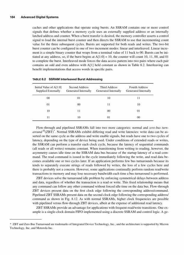
184 Advanced Digital Systems
caches and other applications that operate using bursts. An SSRAM contains one or more controlsignals that defines whether a memory cycle uses an externally supplied address or an internallylatched address and counter. When a burst transfer is desired, the memory controller asserts a controlsignal to load the internal burst counter and then directs the SSRAM to use that incrementing countvalue for the three subsequent cycles. Bursts are supported for both reads and writes. The two-bitburst counter can be configured in one of two increment modes: linear and interleaved. Linear incre-ment is a simple binary counter that wraps from a terminal value of 11 back to 00. Bursts can be ini-tiated at any address, so, if the burst begins at A[1:0] = 10, the counter will count 10, 11, 00, and 01to complete the burst. Interleaved mode forces the data access pattern into two pairs where each paircontains an odd and even address with A[1] held constant as shown in Table 8.2. Interleaving canbenefit implementations that access words in specific pairs.
Flow-through and pipelined SSRAMs fall into two more categories: normal and
zero-bus turn-around
®
(ZBT)
*
. Normal SSRAMs exhibit differing read and write latencies: write data can be as-serted on the same cycle as the address and write enable signals, but reads have one to two cycles oflatency, depending on the type of device being used. Under conditions of extended reads or writes,the SSRAM can perform a transfer each clock cycle, because the latency of sequential commands(all reads or all writes) remains constant. When transitioning from writing to reading, however, theasymmetry causes idle time on the SSRAM data bus because of the startup latency of a read com-mand. The read command is issued in the cycle immediately following the write, and read data be-comes available one or two cycles later. If an application performs few bus turnarounds because itstends to separately execute strings of reads followed by writes, the loss of a few cycles here andthere is probably not a concern. However, some applications continually perform random read/writetransactions to memory and may lose necessary bandwidth each time a bus turnaround is performed.
ZBT devices solve the turnaround idle problem by enforcing symmetrical delays between addressand data, regardless of whether the transaction is a read or write. This fixed relationship means thatany command can follow any other command without forced idle time on the data bus. Flow-throughZBT devices present data on the first clock edge following the corresponding address/command.Pipelined ZBT SSRAMs present data on the second clock edge following the corresponding address/command as shown in Fig. 8.12. As with normal SSRAMs, higher clock frequencies are possiblewith pipelined versus flow-through ZBT devices, albeit at the expense of additional read latency.
ZBT SSRAMs provide an advantage for applications with frequent read/write transitions. One ex-ample is a single-clock domain FIFO implemented using a discrete SSRAM and control logic. A ge-
TABLE
8.2 SSRAM Interleaved Burst Addressing
Initial Value of A[1:0]Supplied Externally
Second AddressGenerated Internally
Third AddressGenerated Internally
Fourth AddressGenerated Internally
00 01 10 11
01 00 11 10
10 11 00 01
11 10 01 00
* ZBT and Zero Bus Turnaround are trademarks of Integrated Device Technology, Inc., and the architecture is supported by MicronTechnology, Inc. and Motorola Inc.
-Balch.book Page 184 Thursday, May 15, 2003 3:46 PM
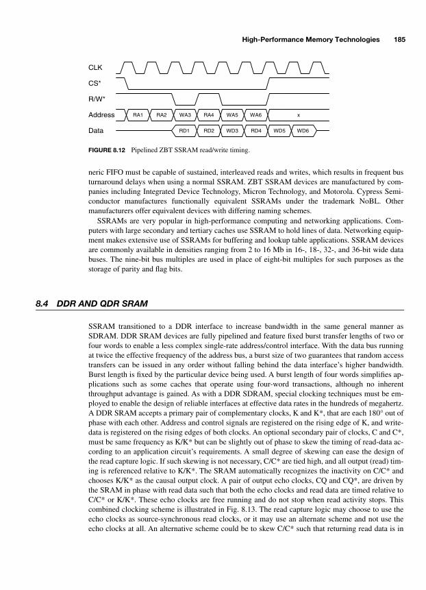
High-Performance Memory Technologies 185
neric FIFO must be capable of sustained, interleaved reads and writes, which results in frequent busturnaround delays when using a normal SSRAM. ZBT SSRAM devices are manufactured by com-panies including Integrated Device Technology, Micron Technology, and Motorola. Cypress Semi-conductor manufactures functionally equivalent SSRAMs under the trademark NoBL. Othermanufacturers offer equivalent devices with differing naming schemes.
SSRAMs are very popular in high-performance computing and networking applications. Com-puters with large secondary and tertiary caches use SSRAM to hold lines of data. Networking equip-ment makes extensive use of SSRAMs for buffering and lookup table applications. SSRAM devicesare commonly available in densities ranging from 2 to 16 Mb in 16-, 18-, 32-, and 36-bit wide databuses. The nine-bit bus multiples are used in place of eight-bit multiples for such purposes as thestorage of parity and flag bits.
8.4 DDR AND QDR SRAM
SSRAM transitioned to a DDR interface to increase bandwidth in the same general manner asSDRAM. DDR SRAM devices are fully pipelined and feature fixed burst transfer lengths of two orfour words to enable a less complex single-rate address/control interface. With the data bus runningat twice the effective frequency of the address bus, a burst size of two guarantees that random accesstransfers can be issued in any order without falling behind the data interface’s higher bandwidth.Burst length is fixed by the particular device being used. A burst length of four words simplifies ap-plications such as some caches that operate using four-word transactions, although no inherentthroughput advantage is gained. As with a DDR SDRAM, special clocking techniques must be em-ployed to enable the design of reliable interfaces at effective data rates in the hundreds of megahertz.A DDR SRAM accepts a primary pair of complementary clocks, K and K*, that are each 180° out ofphase with each other. Address and control signals are registered on the rising edge of K, and write-data is registered on the rising edges of both clocks. An optional secondary pair of clocks, C and C*,must be same frequency as K/K* but can be slightly out of phase to skew the timing of read-data ac-cording to an application circuit’s requirements. A small degree of skewing can ease the design ofthe read capture logic. If such skewing is not necessary, C/C* are tied high, and all output (read) tim-ing is referenced relative to K/K*. The SRAM automatically recognizes the inactivity on C/C* andchooses K/K* as the causal output clock. A pair of output echo clocks, CQ and CQ*, are driven bythe SRAM in phase with read data such that both the echo clocks and read data are timed relative toC/C* or K/K*. These echo clocks are free running and do not stop when read activity stops. Thiscombined clocking scheme is illustrated in Fig. 8.13. The read capture logic may choose to use theecho clocks as source-synchronous read clocks, or it may use an alternate scheme and not use theecho clocks at all. An alternative scheme could be to skew C/C* such that returning read data is in
Address
CLK
RA1 x
Data
CS*
RD1
R/W*
RA2 WA3 RA4 WA5 WA6
RD2 WD3 RD4 WD5 WD6
FIGURE 8.12 Pipelined ZBT SSRAM read/write timing.
-Balch.book Page 185 Thursday, May 15, 2003 3:46 PM
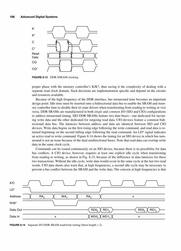
186 Advanced Digital Systems
proper phase with the memory controller’s K/K*, thus saving it the complexity of dealing with aseparate read clock domain. Such decisions are implementation specific and depend on the circuitsand resources available.
Because of the high frequency of the DDR interface, bus turnaround time becomes an importantdesign point. Idle time must be inserted onto a bidirectional data bus to enable the SRAM and mem-ory controller time to disable their tri-state drivers when transitioning from reading to writing or viceversa. DDR SRAMs are manufactured in both
single
and
common I/O
(SIO and CIO) configurationsto address turnaround timing. SIO DDR SRAMs feature two data buses—one dedicated for incom-ing write data and the other dedicated for outgoing read data. CIO devices feature a common bidi-rectional data bus. The latencies between address and data are identical between SIO and CIOdevices. Write data begins on the first rising edge following the write command, and read data is re-turned beginning on the second falling edge following the read command. An LD* signal indicatesan active read or write command. Figure 8.14 shows the timing for an SIO device in which bus turn-around is not an issue because of the dual unidirectional buses. Note that read data can overlap writedata in the same clock cycle.
Commands can be issued continuously on an SIO device, because there is no possibility for databus conflicts. A CIO device, however, requires at least one explicit idle cycle when transitioningfrom reading to writing, as shown in Fig. 8.15, because of the difference in data latencies for thesetwo transactions. Without the idle cycle, write data would occur in the same cycle at the last two readwords. CIO data sheets also warn that, at high frequencies, a second idle cycle may be necessary toprevent a bus conflict between the SRAM and the write data. The concern at high frequencies is that
K
C
K*
C*
CQ
CQ*
ReadData
FIGURE 8.13 DDR SSRAM clocking.
K/C
Data Out
R/W*
Address
LD*
RAX x
Data In
RD0X RD1X
WAY RAZ
RD0Z RD1Z
WD0Y WD1Y xx
FIGURE 8.14 Separate I/O DDR SRAM read/write timing (burst length = 2).
-Balch.book Page 186 Thursday, May 15, 2003 3:46 PM

High-Performance Memory Technologies 187
the SRAM may not be able to turn off its tri-state drivers in time for write data being driven immedi-ately on the next cycle.
High data transfer rates are possible with CIO DDR SRAM in purely random transactions.Grouping multiple reads and writes into separate groups increases the available bandwidth by mini-mizing bus turnaround delays associated with read/write transitions. CIO devices have a distinct ad-vantage in reduced signal count because of a single data bus. Balancing this out is the complexity ofhandling bus turnaround and somewhat reduced bandwidth in truly random transfer patterns.
SIO DDR SRAM provides a definite performance advantage in certain applications at the cost ofadditional signal and pin count. The concept of dual data interfaces was taken a step farther with thedevelopment of
quad data rate
TM
(QDR) SRAM technology, where the goal is to enable full utiliza-tion of the read and write data interfaces.
*
QDR devices are manufactured with fixed two- or four-word bursts. The address/control interface is designed so that enough commands can be issued tokeep both data interfaces fully utilized. A four-word burst QDR SRAM is very similar to an SIODDR SRAM if one were to be made with a four-word burst size. The difference is that, rather thanhaving a R/W* select signal and an activation signal (LD*), the QDR devices implement separateread and write enables. A new command is presented during each clock cycle such that it takes twocycles to issue both a read and a write command. This frequency of commands matches perfectlywith the four-word burst nature of the dual data interfaces. Each read or write command transfersfour words at DDR, thereby occupying two whole clock cycles. Therefore, a read command can beissued once every two cycles, and it takes two cycles to execute. The same holds true for a writecommand. A two-word burst QDR SRAM differs from the four-word variety in that its address/control interface is dual rate to allow commands to be issued twice as fast to keep up with the shortertransfer duration of one cycle (two words at DDR complete in one whole cycle). Figure 8.16 showsthe timing for a four-word burst QDR SRAM. If an application can make efficient use of a four-word
* QDR is a trademark of Cypress, IDT, Micron Technology, NEC, and Samsung.
K/C
Data
R/W*
Address
LD*
RAX x
RD0X RD1X
WAY RAZ
RD0Z RD1ZWD0Y WD1Y
x
FIGURE 8.15 Common I/O DDR SRAM read/write timing (burst length = 2).
K/C
Data Out
WR*
Address RAW x
Data In
RD0W RD1W
WAX RAY
WD0X WD1Xx
RD*
WAZ
RD2W RD3W RD0Y RD1Y RD2Y RD3Y
WD2X WD3X WD0Z WD1Z WD2Z WD3Z x
FIGURE 8.16 QDR SRAM read/write timing (burst length = 4).
-Balch.book Page 187 Thursday, May 15, 2003 3:46 PM
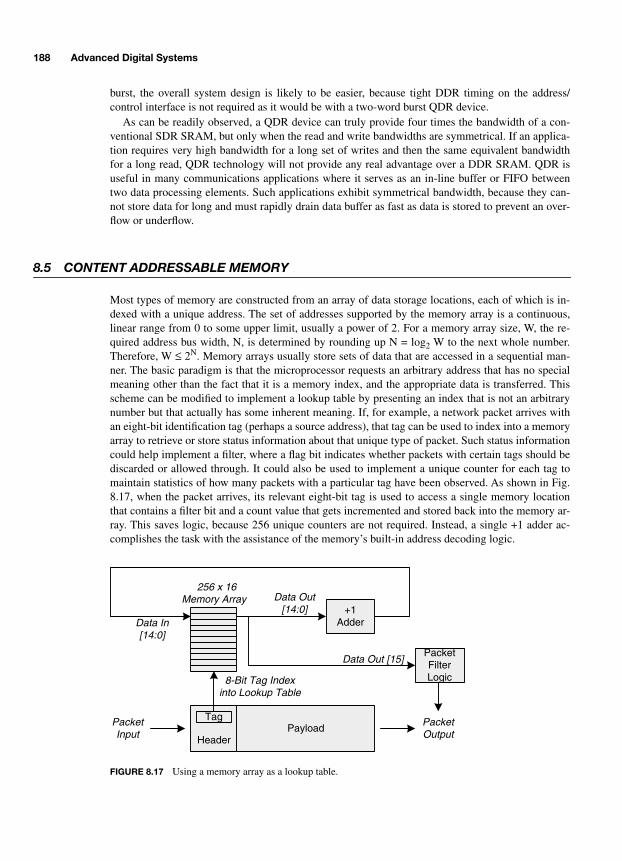
188 Advanced Digital Systems
burst, the overall system design is likely to be easier, because tight DDR timing on the address/control interface is not required as it would be with a two-word burst QDR device.
As can be readily observed, a QDR device can truly provide four times the bandwidth of a con-ventional SDR SRAM, but only when the read and write bandwidths are symmetrical. If an applica-tion requires very high bandwidth for a long set of writes and then the same equivalent bandwidthfor a long read, QDR technology will not provide any real advantage over a DDR SRAM. QDR isuseful in many communications applications where it serves as an in-line buffer or FIFO betweentwo data processing elements. Such applications exhibit symmetrical bandwidth, because they can-not store data for long and must rapidly drain data buffer as fast as data is stored to prevent an over-flow or underflow.
8.5 CONTENT ADDRESSABLE MEMORY
Most types of memory are constructed from an array of data storage locations, each of which is in-dexed with a unique address. The set of addresses supported by the memory array is a continuous,linear range from 0 to some upper limit, usually a power of 2. For a memory array size, W, the re-quired address bus width, N, is determined by rounding up N = log
2
W to the next whole number.Therefore, W
≤
2
N
. Memory arrays usually store sets of data that are accessed in a sequential man-ner. The basic paradigm is that the microprocessor requests an arbitrary address that has no specialmeaning other than the fact that it is a memory index, and the appropriate data is transferred. Thisscheme can be modified to implement a lookup table by presenting an index that is not an arbitrarynumber but that actually has some inherent meaning. If, for example, a network packet arrives withan eight-bit identification tag (perhaps a source address), that tag can be used to index into a memoryarray to retrieve or store status information about that unique type of packet. Such status informationcould help implement a filter, where a flag bit indicates whether packets with certain tags should bediscarded or allowed through. It could also be used to implement a unique counter for each tag tomaintain statistics of how many packets with a particular tag have been observed. As shown in Fig.8.17, when the packet arrives, its relevant eight-bit tag is used to access a single memory locationthat contains a filter bit and a count value that gets incremented and stored back into the memory ar-ray. This saves logic, because 256 unique counters are not required. Instead, a single +1 adder ac-complishes the task with the assistance of the memory’s built-in address decoding logic.
PayloadHeader
Tag
256 x 16Memory Array
8-Bit Tag Indexinto Lookup Table
+1Adder
Data Out[14:0]
Data In[14:0]
PacketInput
PacketOutput
PacketFilterLogic
Data Out [15]
FIGURE 8.17 Using a memory array as a lookup table.
-Balch.book Page 188 Thursday, May 15, 2003 3:46 PM

High-Performance Memory Technologies 189
Such lookup tables are common in communication systems where decisions are made and statis-tics gathered according to the unique tags and network addresses present in each packet’s header.When the size of a tag is bounded at a manageable width, a conventional memory array can be usedto implement a lookup table. However, as tags grow to 16, 32, 64, 128, or more bits, the requiredmemory size becomes quite impractical. The example in Fig. 8.17 would require 8 GB of memory ifthe tag width increased from 8 to 32 bits! If all 2
32
tag permutations need to be accounted for inde-pendently, there would be no avoiding a large memory array. However, the majority of such lookuptable applications handle a small fraction of the total set of permutations. The working set of tagssparsely populates the complete defined set of tags. So the question becomes how to rapidly indexinto a memory array with an N-bit tag where the array size is much less than 2
N
.A
content addressable memory
(CAM) solves this problem with an array of fully associative tagsand optional corresponding data entries as shown in Fig. 8.18. Instead of decoding 2
N
unique loca-tions based on an N-bit tag, each CAM entry simultaneously matches its own tag to the one pre-sented. The entry whose tag matches is the one that presents its associated data at the output and theone that can have its data modified as well. Alternatively, a CAM may simply return the index of thematched or winning entry in the array, if the specific device does not have any data associated witheach entry. There is substantial overhead in providing each entry with a unique tag and matchinglogic, making CAMs substantially more expensive than conventional memories on a per-bit basis.Their increased cost is justified in those applications that require rapid searching of large yetsparsely populated index ranges.
Unlike a conventional memory, a CAM must be managed by the system’s hardware and/or soft-ware to function properly. The system must load the CAM entries with relevant tags and data. Careshould be taken to keep tags unique, because there is no standard means of resolving the case inwhich two entries’ tags match the tag input. Individual CAM implementations may specify howsuch conflicts are resolved. Some CAMs handle read/write maintenance functions through the sameinterface that tags are presented and matched. Other implementations provide a separate mainte-nance port. Having a separate maintenance port increases the number of pins on the CAM, addingcomplexity to the circuit board wiring, but it may decrease overall system complexity, because main-tenance logic and data logic paths do not have to be shared.
CAM tags and matching logic can be constructed in either a
binary
or
ternary
manner. A binaryCAM implements a standard tag of arbitrary width and a valid bit. These CAMs are well suited tosituations in which exact tag matches are desired. A ternary CAM doubles the number of tag bits to
TagInput
MatchedData
SearchSuccessful
Tag Address/DataValid/Match Logic z
Tag Address/DataValid/Match Logic z
Tag Address/DataValid/Match Logic z
Tag Address/DataValid/Match Logic z
FIGURE 8.18 Basic CAM architecture.
-Balch.book Page 189 Thursday, May 15, 2003 3:46 PM
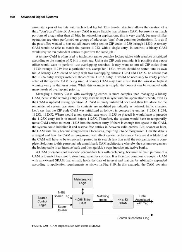
190 Advanced Digital Systems
associate a pair of tag bits with each actual tag bit. This two-bit structure allows the creation of athird “don’t care” state, X. A ternary CAM is more flexible than a binary CAM, because it can matchportions of a tag rather than all bits. In networking applications, this is very useful, because similaroperations are often performed on groups of addresses (tags) from common destinations. It is as ifthe post office wanted to sort out all letters being sent to ZIP codes 11230 through 11239. A ternaryCAM would be able to match the pattern 1123X with a single entry. In contrast, a binary CAMwould require ten redundant entries to perform the same job.
A ternary CAM is often used to implement rather complex lookup tables with searches prioritizedaccording to the number of X bits in each tag. Using the ZIP code example, it is possible that a postoffice would want to perform two overlapping searches. It may want to sort all ZIP codes from11230 through 11239 into a particular bin, except for 11234, which should be sorted into its ownbin. A ternary CAM could be setup with two overlapping entries: 11234 and 1123X. To ensure thatthe 11234 entry always matched ahead of the 1123X entry, it would be necessary to verify propersetup of the specific CAM being used. A ternary CAM may have a rule that the lowest or highestwinning entry in the array wins. While this example is simple, the concept can be extended withmany levels of overlap and priority.
Managing a ternary CAM with overlapping entries is more complex than managing a binaryCAM, because the winning entry priority must be kept in sync with the application’s needs, even asthe CAM is updated during operation. A CAM is rarely initialized once and then left alone for theremainder of system operation. Its contents are modified periodically as network traffic changes.Let’s say that the ZIP code CAM was initialized as follows in consecutive entries: 1121X, 11234,1123X, 112XX. Where would a new special-case entry 11235 be placed? It would have to precedethe 1123X entry for it to match before 1123X. Therefore, the system would have to temporarilymove CAM entries to insert 11235 into the correct entry. If there is enough free space in the CAM,the system could initialize it and reserve free entries in between valid entries. But, sooner or later,the CAM will likely become congested in a local area, requiring it to be reorganized. How the data isarranged and how the CAM is reorganized will affect system performance, because it is likely thatthe CAM will have to be temporarily paused in its search function until the reorganization is com-plete. Solutions to this pause include a multibank CAM architecture whereby the system reorganizesthe lookup table in an inactive bank and then quickly swaps inactive and active banks.
A CAM often does not associate general data bits with each entry, because the main purpose of aCAM is to match tags, not to store large quantities of data. It is therefore common to couple a CAMwith an external SRAM that actually holds the data of interest and that can be arbitrarily expandedaccording to application requirements as shown in Fig. 8.19. In this example, the CAM contains
4,096 EntryCAM
4k x 32SRAM
MatchingIndex
N-BitSearch Tag
MaintenanceLogic
DataAssociated
with Tag
Search Successful Flag
SearchControlLogic Search
Enable
FIGURE 8.19 CAM augmentation with external SRAM.
-Balch.book Page 190 Thursday, May 15, 2003 3:46 PM

High-Performance Memory Technologies 191
4,096 entries and returns a 12-bit index when a tag has been successfully matched. This index servesas the address of an SRAM that has a 32-bit data path as required by the application.
When combined with conventional memory and some control logic, a CAM subsystem is some-times referred to as a
search engine
. A search engine is differentiated from a stand-alone CAM bybeing capable of semi-autonomous lookups on behalf of another entity such as data processing logicin either hardware or software. A search engine’s control logic can be as simple as accepting a searchtag and then returning data along with a success flag. It can get more complex to include specific ta-ble maintenance functions so that CAM overhead operations are completely offloaded from the dataprocessing logic. Search engines are especially useful when interfacing with special-purpose
net-work processor
devices. These processors run software to parse packets and make decisions abouthow each packet should be handled in the system. The tag lookup function is offloaded to a searchengine when there is not enough time for a software algorithm to search a large table.
-Balch.book Page 191 Thursday, May 15, 2003 3:46 PM

This page intentionally left blank.
193
CHAPTER 9
Networking
Data communications is an essential component of every digital system. Some systems realize com-munications by direct interaction with the environment and some with the exchange of removablestorage media such as tapes, disks, or memory modules. Many systems engage in data transfer that ismore real-time in nature. When these communications begin to involve multiple end-points, high-speed transfers, and the need for reliable carriage of that data, the set of technologies that are broadlyknown as networking become directly relevant.
There is probably no single definition of networking that can always identify when it is or is notneeded—the universe of applications is too diverse for such rigid definitions. The purpose of thischapter is to introduce mainstream networking concepts so that you can make the decision ofwhether a particular application demands networking or a simpler exchange of bits and bytes. Net-working technologies blend hardware and software into algorithms that are implemented by either orboth resources, depending on the specific context. Because of limitations of space and scope, thischapter concentrates on the hardware aspect of networking and how hardware is used to support theformats, protocols, and algorithms that make networking the flexible technology that it is.
The discussion begins with protocol layers to understand the separate logical functions that com-pose a network. Ethernet is frequently used as an example to further clarify networking concepts be-cause of its ubiquity. Hardware support for networking most commonly resides at the lower layers ofthe protocol stack. The bulk of the chapter is concerned with transmission, recovery, and verificationof data on the wire—essential tasks that serve as the foundation of data transfer. A brief presentationof Ethernet closes the chapter to provide an illustration of how networking technology functions inthe real world.
9.1 PROTOCOL LAYERS ONE AND TWO
Networking systems can be highly complex and include many different hardware and software com-ponents. To facilitate the analysis and design of such systems, major functional sections are sepa-rated into
layers
whose definitions are reasonably standardized across the industry. Multiple layersare arranged from the lowest level on the bottom to the highest level on the top in a conceptual
pro-tocol stack
. To transfer data from an application running on one computer to that on another, the datadescends the stack’s layers on one computer and then ascends the stack on the destination computer.The industry standard network stack definition is the
Open System Interconnection
(OSI) referencemodel shown in Fig. 9.1.
As with most conceptual classifications, it is important to recognize that not all networkingschemes and implementations adhere strictly to the OSI seven-layer model. Some schemes maymerge one or more layers together, thereby reducing the number of formally defined layers. Others
-Balch.book Page 193 Thursday, May 15, 2003 3:46 PM
Copyright 2003 by The McGraw-Hill Companies, Inc. Click Here for Terms of Use.

194 Advanced Digital Systems
may segment an OSI layer into multiple sublayers. The consistency of definitions decreases as onemoves up the stack, because of functional protocol variations.
Layer one, the
physical layer
, comprises the electromechanical characteristics of the mediumused to convey bits of information. The use of twisted pair cable, the amplitude of 1s and 0s, and as-sociated connectors and transducers are examples of that which is specified in the physical layer.Channel coding, how the bits are represented on the physical medium, is usually classified as part ofthe physical layer.
The
data link layer
, layer two, encompasses the control logic and frame formatting that enablesdata to be injected into the network’s physical layer and retrieved at the destination node. Layer-twofunctions are usually handled by a
media access controller
(MAC), a hardware device that containsall of the logic necessary to gain access to the network medium, properly format and transmit aframe, and properly detect and process an incoming frame. Network frame formats specify data linklayer characteristics. Link level error detection mechanisms such as checksums and CRCs (more onthese later) are generated and verified by the MAC. Node addresses, called
MAC addresses
in Ether-net networks, are layer-two constructs that uniquely identify individual nodes. Layer-two functionsare usually handled in hardware, because they are repetitive, high-frequency, and time-critical oper-ations. The data link layer is closely tied to the topology of the network because of its handling ofaccess control functions and unique node addresses. Network
switches
operate at layer two by know-ing which node address is connected to which port and then directing traffic to the relevant port. Ifport 20 of a switch is connected to node 87, all frames that enter the switch destined for node 87 willbe sent out port 20. Because it is necessary to maintain unique layer-two addresses, they are gener-ally not under the control of the user but rather are configured by the manufacturer. In the case ofEthernet, each manufacturer of equipment licenses an arbitrary range of MAC addresses from theIEEE and then assigns them one at a time as products roll off the assembly lines.
9.2 PROTOCOL LAYERS THREE AND FOUR
More flexible communications are possible when a protocol is not tied too closely to network topol-ogy or even the type of network accomplishing the exchange of information. The
network layer
,layer three, enables nodes to establish end-to-end connections without strict knowledge of the net-work topology. Layer-three packets are encapsulated within the payload of a layer-two frame. Thepackets typically contain their own header, payload, and sometimes a trailer as well. Perhaps themost common example of a layer-three protocol is
Internet Protocol
(IP). IP packets consist of a
Physical (Layer 1)
Data Link (Layer 2)
Network (Layer 3)
Transport (Layer 4)
Session (Layer 5)
Presentation (Layer 6)
Application (Layer 7)
FIGURE 9.1 OSI seven-layer model.
-Balch.book Page 194 Thursday, May 15, 2003 3:46 PM
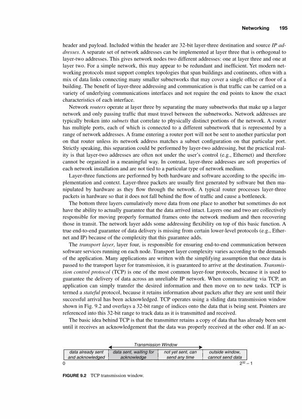
Networking 195
header and payload. Included within the header are 32-bit layer-three destination and source
IP ad-dresses
. A separate set of network addresses can be implemented at layer three that is orthogonal tolayer-two addresses. This gives network nodes two different addresses: one at layer three and one atlayer two. For a simple network, this may appear to be redundant and inefficient. Yet modern net-working protocols must support complex topologies that span buildings and continents, often with amix of data links connecting many smaller subnetworks that may cover a single office or floor of abuilding. The benefit of layer-three addressing and communication is that traffic can be carried on avariety of underlying communications interfaces and not require the end points to know the exactcharacteristics of each interface.
Network
routers
operate at layer three by separating the many subnetworks that make up a largernetwork and only passing traffic that must travel between the subnetworks. Network addresses aretypically broken into
subnets
that correlate to physically distinct portions of the network. A routerhas multiple ports, each of which is connected to a different subnetwork that is represented by arange of network addresses. A frame entering a router port will not be sent to another particular porton that router unless its network address matches a subnet configuration on that particular port.Strictly speaking, this separation could be performed by layer-two addressing, but the practical real-ity is that layer-two addresses are often not under the user’s control (e.g., Ethernet) and thereforecannot be organized in a meaningful way. In contrast, layer-three addresses are soft properties ofeach network installation and are not tied to a particular type of network medium.
Layer-three functions are performed by both hardware and software according to the specific im-plementation and context. Layer-three packets are usually first generated by software but then ma-nipulated by hardware as they flow through the network. A typical router processes layer-threepackets in hardware so that it does not fall behind the flow of traffic and cause a bottleneck.
The bottom three layers cumulatively move data from one place to another but sometimes do nothave the ability to actually guarantee that the data arrived intact. Layers one and two are collectivelyresponsible for moving properly formatted frames onto the network medium and then recoveringthose in transit. The network layer adds some addressing flexibility on top of this basic function. Atrue end-to-end guarantee of data delivery is missing from certain lower-level protocols (e.g., Ether-net and IP) because of the complexity that this guarantee adds.
The
transport layer
, layer four, is responsible for ensuring end-to-end communication betweensoftware services running on each node. Transport layer complexity varies according to the demandsof the application. Many applications are written with the simplifying assumption that once data ispassed to the transport layer for transmission, it is guaranteed to arrive at the destination.
Transmis-sion control protocol
(TCP) is one of the most common layer-four protocols, because it is used toguarantee the delivery of data across an unreliable IP network. When communicating via TCP, anapplication can simply transfer the desired information and then move on to new tasks. TCP istermed a
stateful
protocol, because it retains information about packets after they are sent until theirsuccessful arrival has been acknowledged. TCP operates using a sliding data transmission windowshown in Fig. 9.2 and overlays a 32-bit range of indices onto the data that is being sent. Pointers arereferenced into this 32-bit range to track data as it is transmitted and received.
The basic idea behind TCP is that the transmitter retains a copy of data that has already been sentuntil it receives an acknowledgement that the data was properly received at the other end. If an ac-
outside window,cannot send data
data already sentand acknowledged
not yet sent, cansend any time
data sent, waiting foracknowledge
0 232 – 1
Transmission Window
FIGURE 9.2 TCP transmission window.
-Balch.book Page 195 Thursday, May 15, 2003 3:46 PM
196 Advanced Digital Systems
knowledgement message is not received after a certain amount of time, the data is retransmitted.TCP moves the complexity of guaranteeing end-to-end data delivery into software instead of into theunderlying network hardware, which is often Ethernet. When Ethernet was developed in the 1970s,the cost of logic gates was much higher than it is now, and there was a strong incentive to simplifyhardware wherever possible.
The transmission window size is established by the receiver via messages that are sent to thetransmitter during connection negotiation and subsequent communications. For a receiver to adver-tise a certain window size, it must have sufficient buffering to hold the entire contents of the window.Once the transmitter is informed of the available transmission window, it may begin sending asmuch data that can fit within the window. Each time the transmitter sends data, it marks that packetwith a 32-bit
sequence number
. This sequence number identifies the 32-bit index that corresponds tothe first data byte in the payload and enables the receiver to reconstruct the original data in its propersequence. When the receiver has successfully received a contiguous block of data starting from theleft side of the window, it sends an acknowledgement message with a 32-bit
acknowledgement num-ber
marking the next highest expected sequence number of data. In other words, the acknowledge-ment number corresponds to the index of the highest byte successfully received plus 1. Uponreceiving this message, the transmitter is able to slide the left side of the window up to the acknowl-edgment number and discard the data in its buffer that now falls outside the window on the left side.The receiver must continually extend the right side of the window to maintain data flow. If the re-ceiver does not slide the right side of the window open, the left side will continue to advance untilthe window closes, preventing new data from being transmitted.
Guaranteeing end-to-end delivery of data on an inherently unreliable network adds substantialcomplexity to transport protocol drivers. These functions were traditionally handled by software.However, certain high-performance applications benefit from accelerating TCP in hardware—a taskthat is decidedly nontrivial.
There are also applications that do not require a transport protocol to guarantee delivery of data.The reason for this may be that the TCP driver is too cumbersome to implement, a proprietary mech-anism is preferable, or the underlying network is, in fact, reliable. In such cases, it is unnecessaryand often undesired to implement a complex protocol such as TCP. TCP’s companion protocol fornonguaranteed transmission is called
user datagram protocol
(UDP). UDP is used along with IP net-works to send simple messages over unreliable networks or critical data over reliable networks. It isa stateless protocol, because it simply wraps the data in a header and sends it to the network layerwithout retaining any information about delivery. As such, there is no sliding transmission windowconcept and no need for bidirectional communication at the transport layer.
Aside from guaranteeing delivery, many transport protocols implement a higher level of address-ing, often referred to as
ports
or
sockets
. An individual node has a single network address associatedwith it. However, each application on that node can have its own associated port or socket number.These constructs allow the transport layer to direct data flows to the appropriate application on thedestination node. Rather than sending each packet that arrives to each application, an application es-tablishes a port or socket number and, henceforth, all network traffic destined for that application ismarked with the correct port or socket number.
Layers five, six, and seven are more context specific and principally involve application and net-work driver software as part of a computer’s operating system and network interface subsystem.From a design perspective, the degree of hardware responsibility decreases as one ascends the stack.Less-expensive systems will often try to use as little hardware as possible, resulting in the bare es-sentials of the physical and data link layers being implemented in hardware. Such systems offload asmany functions as possible onto software to save cost, albeit at the expense of reducing the through-put of the network interface. As higher levels of throughput are desired, more hardware creeps intothe bottom layers. On general-purpose computers, the network and transport layers are usually im-
-Balch.book Page 196 Thursday, May 15, 2003 3:46 PM

Networking 197
plemented in network driver software. However, on special-purpose platforms where high band-width is critical, many layer-three and layer-four functions are accelerated by hardware. How thesetrade-offs are made depends on the exact type of networking scheme being implemented.
9.3 PHYSICAL MEDIA
Most wired networking schemes use high-speed unidirectional serial data channels as their physicalcommunication medium. A pair of unidirectional channels is commonly used to provide bidirec-tional communications between end points. Despite the fact that it is technically feasible to use a sin-gle channel in a bidirectional mode, it is easier to design electronics and associated physicalapparatus that implement either a transmitter or receiver at each end of a cable, but not both. Thecost of mandating a pair of cables instead of a single cable is not very burdensome, because cablesare commonly manufactured as a bundle and are handled as a single unit in wiring conduits and con-nection points. Two ubiquitous types of media are twisted-pair wiring and fiber optic cable. It iscommon to find a single cable bundle containing two or more twisted pairs or a pair of fiber opticstrands. Twisted-pair and fiber can often be used interchangeably by a network transceiver as long asthe appropriate transducer properly converts between the transceiver’s electrical signaling and themedium’s signaling. In the case of twisted pair, this conversion may consist of only amplificationand noise filtering. A fiber optic cable is somewhat more complex in that it requires an electro-opti-cal conversion.
Twisted pair wiring is used in conjunction with differential signaling to provide improved noiseimmunity versus a single-ended, or unbalanced, transmission medium. As network data rates haveincreased, twisted pair wiring technology has kept pace with improved quality of manufacture tosupport higher bandwidths. When the majority of Ethernet connections ran at 10 Mbps (10BASE-T),
unshielded twisted pair
(UTP)
category-3
(CAT3) was a common interconnect medium. UTPwiring does not contain any surrounding grounded metal shield for added noise protection. As100BASE-T emerged, wiring technology moved to CAT5, and this has remained the most commonUTP medium for some time. CAT5 has largely replaced CAT3, because the cost differential is slim,and it exhibits better performance as a result of more twists per unit length and improved structuralintegrity to maintain the desired electrical characteristics over time and handling. Enhanced UTPproducts including CAT5e and CAT6 are emerging because of the popularity of gigabit Ethernetover twisted pair (1000BASE-T). While most twisted pair is unshielded, shielded varieties (STP)are used in specific applications. UTP is a favored wiring technology because of its relatively lowcost and ease of handling: connections can be made by crimping or punching the wires onto con-nector terminals. The disadvantage of copper media is their susceptibility to noise and attenuationof signals over moderate distances. These characteristics limit total UTP cable length to 100 m incommon Ethernet applications.
Bandwidth and distance are inversely related by the inherent characteristics of a given transmis-sion medium. As distances increase, signal degradation increases, which reduces the available band-width of the channel. Fiber optic cabling is used to overcome the bandwidth and distance limitationsof twisted pair wiring because of its immunity to electrical noise and very low optical attenuationover distance. Fiber optic cable is generally constructed from high-purity glass, but plastic cableshave been used for special short-distance applications. Rather than being a simple extrusion of glass,a fiber optic cable contains two optical elements surrounded by a protective sheath as shown in Fig.9.3a. The inner glass core is differentiated from the outer glass cladding by the fact that one or bothhave been doped with certain molecules to change their indices of refraction. The cladding has alower index of refraction than the core, which causes the great majority of light injected into the core
-Balch.book Page 197 Thursday, May 15, 2003 3:46 PM

198 Advanced Digital Systems
to bounce off the core/cladding boundary as shown in Fig. 9.3b, thereby trapping the light over verylong distances.
Light is injected into the core using either an LED or laser, depending on the required quality ofthe signal. A laser can generate light that is coherent, meaning that its photons are at the same fre-quency and phase. Injecting coherent light into a fiber optic cable reduces the distortion that accu-mulates over distance as photons of different frequency travel through the medium at slightlydifferent velocities. Noncoherent photons that are emitted simultaneously as part of a signal pulsewill arrive at the destination spread slightly apart in time. This spreading makes reconstructing thesignal more difficult at very high frequencies, because signal edges are distorted.
Even when
coherent
light is used, photons can take multiple paths in the core as they bounce offthe core/cladding boundary at different angles. These multiple propagation
modes
cause distortionover distance. To deal with this phenomenon, two types of fiber optic cable are commonly used:
sin-gle-mode
and
multimode
. Single-mode fiber contains a very thin core of approximately 8 to 10 µm indiameter that constrains light to a single propagation mode, thereby reducing distortion. Multimodefiber contains a larger core, typically 62.5 µm, that allows for multiple propagation modes and henceincreased distortion. Single-mode fiber is more expensive than multimode and is used in longer-dis-tance and higher-bandwidth applications as necessary.
Fiber optic cabling is more expensive than copper wire, and the handling of optical connections ismore costly and complex as compared to copper. Splicing a fiber optic cable requires special equip-ment to ensure a clean cut and low-loss junction between two separate cables. The best splice is ob-tained by actually fusing two cables together to form a seamless connection. This is substantiallymore involved than splicing a copper cable, which can be done with fairly simple tools. Fiber opticconnectors are sensitive to dirt and other contaminants that can attenuate the photons’ energy as theypass through. Additionally, fine abrasive particles can scratch the glass faces of optical interfaces,causing permanent damage. Once properly installed and sealed, however, fiber optic cable can actu-ally be more rugged than copper cables because of its insensitivity to oxidation that degrades copperwiring over time. Aside from bandwidth issues, these environmental benefits have resulted in infra-structures such as cable TV being partially reinstalled with fiber to cut long-term maintenance costs.
9.4 CHANNEL CODING
High-speed serial data channels require the basic functionality of a UART, albeit at very high speed,to convert back and forth between serial and parallel data paths. Unlike a UART that typically func-tions at kilobits or a few megabits per second, specialized transceiver ICs called
serializer/deserial-
StructuralSheath
GlassCladding
GlassCore
cladding
cladding
(a) (b)
FIGURE 9.3 Fiber optic cable: (a) cross section and (b) propagation.
-Balch.book Page 198 Thursday, May 15, 2003 3:46 PM

Networking 199
izers
, or
serdes
for short, are manufactured that handle serial rates of multiple gigabits per second.Serdes vendors include AMCC, Conexant, Intel, PMC-Sierra, Texas Instruments, and Vitesse. Tosimplify system design, a serdes accepts a lower-frequency reference clock that is perhaps 1/10 or 1/20 the bit frequency of the serial medium. Parallel data is usually transmitted to the serdes at this ref-erence frequency. For example, the raw bit rate of gigabit Ethernet (IEEE 802.3z) is 1.25 Gbps, but atypical serdes accepts a 125-MHz reference clock and 10 bits per cycle of transmit data. The refer-ence clock is internally multiplied using a phase locked loop (PLL) to achieve the final bit rate. Ageneral serdes block diagram is shown in Fig. 9.4. An optional transmit clock is shown separatelyfrom the reference clock, because some devices support these dual clocks. The benefits of a dual-clock scheme are that a very stable reference clock can be driven by a high-accuracy source sepa-rately from a somewhat noisier source-synchronous transmit clock generated by the data processinglogic. This eases the clock jitter requirements on data processing logic.
A clock recovery circuit in the receiver portion extracts a bit clock from the serial data stream thatis transmitted without a separate clock. This recovery is possible, because the serial data stream isnormally coded with an algorithm that guarantees a certain proportion of state transitions regardlessof the actual data being transferred. Such coding can be performed within the serdes or by externaldata processing logic. Channel coding is necessary for more than clock recovery. Analog circuits inthe signal path, notably transducer and amplifier elements, require a relatively balanced data streamto function optimally. In circuit analysis terms, they work best when the data stream has an averageDC value of 0. This is achieved with a data stream that contains an equal number of 1s and 0s overshort spans of time. If a 1 is represented as a positive voltage and a 0 is represented as a negativevoltage of equal magnitude, equal numbers of 1s and 0s balance out to an average voltage of 0 overtime.
Fortunately, it is possible to encode an arbitrary data stream such that the coded version containsan average DC value of 0, and that data can be restored to its original form with an appropriate de-coding circuit. One fairly simple method of encoding data is through a scrambling polynomial im-
PLL ClockMultiplier
Serial toParallel
Parallel toSerial
Transmit Data
Transmit Clock
Reference Clock
InputRegister
OutputCircuitry
Serial Output
InputCircuitry
Serial Input
ClockRecovery
Circuit
InputRegister
FramingDetection
Logic
Receive Data
Receive Clock
Code Detect
Encoder
Decoder
optional codinglogic
FIGURE 9.4 Serdes block diagram.
-Balch.book Page 199 Thursday, May 15, 2003 3:46 PM
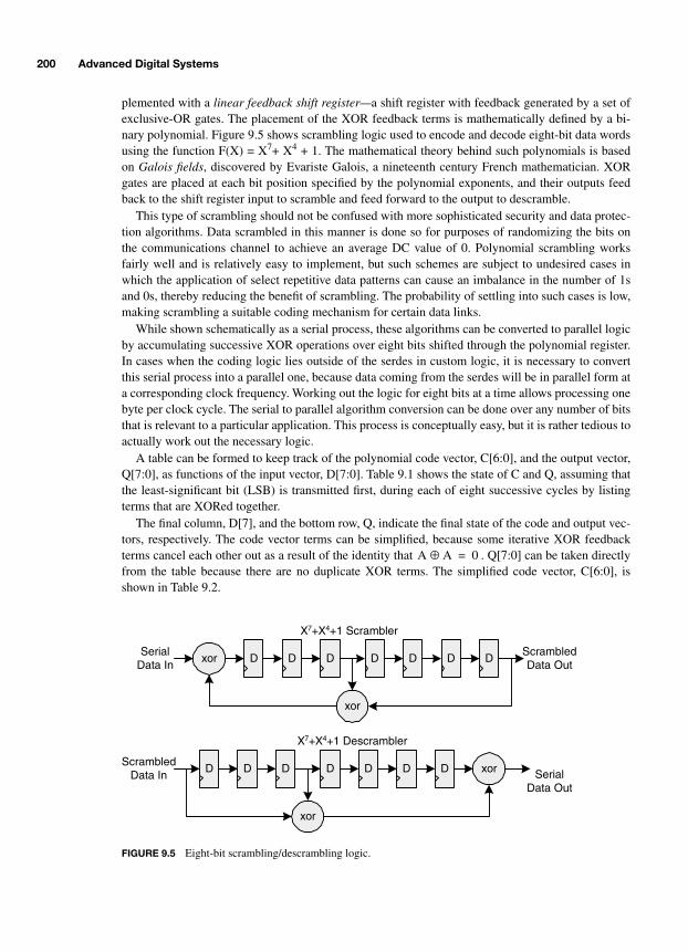
200 Advanced Digital Systems
plemented with a
linear feedback shift register—
a shift register with feedback generated by a set ofexclusive-OR gates. The placement of the XOR feedback terms is mathematically defined by a bi-nary polynomial. Figure 9.5 shows scrambling logic used to encode and decode eight-bit data wordsusing the function F(X) = X
7
+ X
4
+ 1. The mathematical theory behind such polynomials is basedon
Galois fields
, discovered by Evariste Galois, a nineteenth century French mathematician. XORgates are placed at each bit position specified by the polynomial exponents, and their outputs feedback to the shift register input to scramble and feed forward to the output to descramble.
This type of scrambling should not be confused with more sophisticated security and data protec-tion algorithms. Data scrambled in this manner is done so for purposes of randomizing the bits onthe communications channel to achieve an average DC value of 0. Polynomial scrambling worksfairly well and is relatively easy to implement, but such schemes are subject to undesired cases inwhich the application of select repetitive data patterns can cause an imbalance in the number of 1sand 0s, thereby reducing the benefit of scrambling. The probability of settling into such cases is low,making scrambling a suitable coding mechanism for certain data links.
While shown schematically as a serial process, these algorithms can be converted to parallel logicby accumulating successive XOR operations over eight bits shifted through the polynomial register.In cases when the coding logic lies outside of the serdes in custom logic, it is necessary to convertthis serial process into a parallel one, because data coming from the serdes will be in parallel form ata corresponding clock frequency. Working out the logic for eight bits at a time allows processing onebyte per clock cycle. The serial to parallel algorithm conversion can be done over any number of bitsthat is relevant to a particular application. This process is conceptually easy, but it is rather tedious toactually work out the necessary logic.
A table can be formed to keep track of the polynomial code vector, C[6:0], and the output vector,Q[7:0], as functions of the input vector, D[7:0]. Table 9.1 shows the state of C and Q, assuming thatthe least-significant bit (LSB) is transmitted first, during each of eight successive cycles by listingterms that are XORed together.
The final column, D[7], and the bottom row, Q, indicate the final state of the code and output vec-tors, respectively. The code vector terms can be simplified, because some iterative XOR feedbackterms cancel each other out as a result of the identity that . Q[7:0] can be taken directlyfrom the table because there are no duplicate XOR terms. The simplified code vector, C[6:0], isshown in Table 9.2.
SerialData In
ScrambledData Out
X7+X4+1 Scrambler
ScrambledData In Serial
Data Out
xor D
xor
xor
xor
X7+X4+1 Descrambler
D D DD DD
D D D DD DD
FIGURE 9.5 Eight-bit scrambling/descrambling logic.
A A⊕ 0=
-Balch.book Page 200 Thursday, May 15, 2003 3:46 PM

Networking 201
Following the same process, code and output vectors for the associated descrambling logic can bederived as well, the results of which are shown in Table 9.3. In this case, the code vector, C[6:0], iseasy, because it is simply the incoming scrambled data shifted one bit at a time without any XORfeedback terms. The output vector, Q[7:0], is also easier, because the XOR logic feeds forward with-out any iterative feedback terms.
TABLE
9.1 Scrambler Logic State Table
Code/OutputVector Bits
Input Vector Bits, One Each Clock Cycle
D0 D1 D2 D3 D4 D5 D6 D7
C6 C0 D0 C4 C1 D1 C5 C2 D2 C6 C3 D3 C0 D0 C4
C4 D4 C1 D1 C5
C5 D5 C2 D2 C6
C6 D6 C3 D3 C0 D0
C4
C0 D0 C4 D7 C4 D4 C1 D1 C5
C5 C6 C0 D0 C4 C1 D1 C5 C2 D2 C6 C3 D3 C0 D0 C4
C4 D4 C1 D1 C5
C5 D5 C2 D2 C6
C6 D6 C3 D3 C0 D0
C4
C4 C5 C6 C0 D0 C4 C1 D1 C5 C2 D2 C6 C3 D3 C0 D0 C4
C4 D4 C1 D1 C5
C5 D5 C2 D2 C6
C3 C4 C5 C6 C0 D0 C4 C1 D1 C5 C2 D2 C6 C3 D3 C0 D0 C4
C4 D4 C1 D1 C5
C2 C3 C4 C5 C6 C0 D0 C4 C1 D1 C5 C2 D2 C6 C3 D3 C0 D0 C4
C1 C2 C3 C4 C5 C6 C0 D0 C4 C1 D1 C5 C2 D2 C6
C0 C1 C2 C3 C4 C5 C6 C0 D0 C4 C1 D1 C5
Q C0 C1 C2 C3 C4 C5 C6 C0 D0 C4
TABLE
9.2 Simplified Scrambling Code Vector Logic
Code Vector Bits XOR Logic
C6 C0 D0 C1 D1 D4 C5 D7
C5 C0 D0 C3 D3 C4 C6 D6
C4 C2 D2 C5 D5 C6
C3 C1 D1 C4 D4 C5
C2 C0 D0 C3 D3 C4
C1 C2 D2 C6
C0 C1 D1 C5
-Balch.book Page 201 Thursday, May 15, 2003 3:46 PM

202 Advanced Digital Systems
Data that has been encoded must be decoded before framing information can be extracted. There-fore, the serdes’ receiving shift register must begin by performing a simple serial-to-parallel conver-sion until framing information can be extracted after decoding. Prior to the detection of framinginformation, the output of the parallel shift register will be arbitrary data at an arbitrary alignment,because there is no knowledge of where individual bytes of words begin and end in the continuousdata stream. Once a framing sequence has been detected, the shift register can be “snapped” intocorrect alignment, and its output will be properly formatted whole bytes or words.
When reconstructing decoded data, the desired byte alignment will likely span two consecutivebytes as they come straight from the descrambling logic. The most significant bits of a descrambledbyte logically follow the LSB of the next descrambled byte because of the order in which bits areshifted through the scrambler and descrambler. Therefore, when data arrives misaligned at the re-ceiver/descrambler, bytes are reassembled by selecting the correct bits from the most significant bits(MSB) of descrambled byte N and the LSB of descrambled byte N + 1 as shown in Fig. 9.6.
Framing information is not conveyed by the scrambled coding and must therefore be extracted ata higher level. For this reason, certain serdes components that are used in scrambled coding systems
TABLE
9.3 Descrambling Logic Code and Output Vector Logic
Code Vector Bits Shift Logic Output Vector Bits XOR Logic
– – D7 D0 D7 D4
C6 D7 D6 C6 D6 D3
C5 D6 D5 C5 D5 D2
C4 D5 D4 C4 D4 D1
C3 D4 D3 C3 D3 D0
C2 D3 D2 C2 D2 C6
C1 D2 D1 C1 D1 C5
C0 D1 D0 C0 D0 C4
76543210
Descrambled byte N,arrives first
Descrambled byte N + 1,arrives next
76543210
76543210Reassembled byte with
MSB from byte N + 1and LSB from byte N
Time order in which bits are shifted through scrambler/descrambler (LSB first)
FIGURE 9.6 Reassembly of descrambled data.
-Balch.book Page 202 Thursday, May 15, 2003 3:46 PM

Networking 203
do not support any descrambling or framing detection logic, because that logic is application spe-cific. These functions must be implemented by external data processing logic. There are specificcases in which a common class of applications use standard scrambling and framing techniques. Ser-des ICs designed for these applications do support the decoding and framing functions. An exampleof such an application is the transport of serial digital video in a TV studio setting. Companies suchas Gennum Corporation manufacture serdes components with logic that can descramble 10-bit videodata words and recognize framing sequences so that the resulting data stream is cleanly wordaligned and directly usable without further manipulation.
9.5 8B10B CODING
An alternative, more robust coding method is
8B10B coding,
which maps byte values to 10-bitcodes. Unlike polynomial coding that operates on a continuous stream of bits, 8B10B processeseach byte individually. Each coded value is guaranteed to contain either five 0s and five 1s, four 0sand six 1s, or six 0s and four 1s. Therefore, a coded value contains a 0/1 imbalance of at most onebit. Some raw byte values are mapped to a perfectly balanced coded value. Those that map to imbal-anced codes are given two mappings: one with four 0s and six 1s and one with six 0s and four 1s. Aconcept called c
urrent running disparity
(CRD) is used to keep track of whether the last code con-tained a positive (1) or negative (0) imbalance. If a byte passes through the 8B10B encoder and ismapped to a code with four 0s and six 1s, a CRD state bit is set. The next time a byte passes throughthe encoder that has two possible mappings, the negatively imbalanced code will be chosen, andCRD will be cleared. This mechanism ensures that there are an equal number of 1s and 0s over time.
8B10B guarantees a minimum frequency of 0/1/0 transitions within the coded data stream, en-abling reliable recovery of the serial bit clock at the receiver and guaranteeing an average DC valueof 0 across the data stream. In mapping the 256 unique byte values to 10-bit codes, not all 1,024code words are used. Some of these words are undesirable, because they contain greater than a sin-gle bit of 0/1 imbalance. However, some code words are left over that contain valid sequences of 0sand 1s. Rather than leave them unused, these code words are used to carry special values called
spe-cial characters
that can assist in the framing of data on a link. In particular, three special characterscontain a unique
comma pattern
, where the first seven bits of a word contain two bits of one polarityfollowed by five bits of the opposite polarity. This comma pattern is guaranteed not to occur withinany other data words, making it ideal as a marker with which data can be aligned within a serdes. Aserdes that is 8B10B coding aware can search for comma patterns in the data stream and then realignthe data stream such that comma patterns show up in the seven most significant bits of an incomingword. If the data link is properly encoded and is sufficiently free of disruptive noise, this alignmentprocess should have to occur only once and thereafter will be transparent, because the comma pat-terns will already be in the proper bit positions. The benefits of 8B10B coding come with a 20 per-cent overhead penalty, because every eight data bits require ten coded bits. The cost is justified inmany communications systems, because the electrical benefits of a balanced coding scheme enablemore usable bandwidth to be extracted from a medium with a corresponding low bit error rate.
Serdes devices that are 8B10B coding aware contain a framing detection logic block that imple-ments the 8B10B comma alignment function. The actual encoding and decoding may or may not beimplemented in the serdes according to the parameters of the specific device. The comma detectionand alignment function does not require the more complex encoding/decoding functions, becauseonly a simple pattern match is required. A benefit of 8B10B coding is that low-level alignment oper-ations can be performed by generic serdes logic without regard to the actual type of network trafficpassing through the device. For example, Gigabit Ethernet and Fibre Channel (a storage area net-
-Balch.book Page 203 Thursday, May 15, 2003 3:46 PM

204 Advanced Digital Systems
working technology) both utilize 8B10B coding and can therefore take advantage of the same serdesdevices on the market, despite the fact that their frame structures are completely different.
8B10B codes are broken into two sub-blocks to simplify the encoding/decoding process. Ratherthan directly mapping 256 data values into 1,024 code words, the data byte is separated into its threemost-significant bits (designated Y) and its five least-significant bits (designated XX). The data byteis combined with a flag bit to represent its status as either a normal data character or as a specialcharacter. In notational form, a data character is represented as D and a special character as K. Asshown in Fig. 9.7, the eight data bits are assigned letters from H down to A and the sub-blocks areswapped to yield a final notation of D/KXX.Y. For example, the ASCII character Z (0x5A) is splitinto two sub-blocks, 010 (Y) and 11010 (XX), yielding a notation of D26.2.
Once the data or special character has been split into sub-blocks, each sub-block is encoded usingseparate lookup tables whose inputs are the sub-blocks, CRD state information, and the special char-acter flag. Separating the sub-blocks enables smaller lookup tables, which is advantageous fromcomplexity and timing perspectives. The five-bit (XX) sub-block is converted to a six-bit code, andthe three-bit sub-block (Y) is converted to a four-bit code, making ten bits in total. When encodingthe XX sub-block, the CRD bit reflects the running disparity remaining from the previously encodedcharacter. In the case of the Y sub-block, the CRD bit reflects the running disparity remaining fromthe 5B6B encoding of the current character. Tables 9.4 and 9.5 list the 5B6B and 3B4B lookup func-tions. Note that not all special characters are valid and that the CRD bit inverts the code when neces-sary to maintain a balance of 0s and 1s. The encoded bits are referred to by lower-case letters and,when sub-blocks are combined, form a string of bits: a, b, c, d, e, i, f, g, h, j. Encoded words aretransmitted starting with bit “a” and ending with bit “j”.
A special case exists in the 3B4B lookup table when encoding Dxx.7 characters to prevent longstrings of consecutive zeroes or ones. When the CRD is negative and D17.7, D18.7, or D20.7 are be-ing encoded, the alternate 0111 encoding is used instead of 1110. Likewise, when the CRD is posi-tive and D11.7, D13.7, or D14.7 are being encoded, the alternate 1000 encoding is used instead of0001. These exception cases present some additional complexity to the 3B4B translation.
In addition to the 256 possible data characters, 12 special characters are supported. All possibleK28.y characters are supported along with K23.7, K27.7, K29.7 and K30.7. These special charactersare identified by either a unique 5B6B code or a unique 3B4B code. The K28 is the only specialcharacter type with a unique 5B6B encoding. The other special characters are identified, becauseKxx.7 has a unique 3B4B encoding. Recall that not all ten-bit code word permutations can be usedbecause of 0/1 disparity rules inherent in the 8B10B coding algorithm.
There are numerous possible implementations of 8B10B encoder and decoder circuits, and theycan vary by how many bytes are simultaneously processed, the type of lookup table resources avail-able, and the degree of pipelining or other optimization required to achieve the desired throughput. Ahigh-level block diagram of an 8B10B encoder is shown in Fig. 9.8. The larger 5B6B lookup tablecomputes the intermediate CRD´ state that results from mapping the running disparity of the previ-
7 6 5 4 3 2 1 0D/KData
H G FE D C B A
H G F E D C B A
D/KSub-blocks
Notation D/K XX Y.
FIGURE 9.7 8B10B coding notation.
-Balch.book Page 204 Thursday, May 15, 2003 3:46 PM

Networking 205
TABLE
9.4 5B6B Sub-block Encoding
Encoded Valueabcdei
Input CharacterBinary Value
EDCBAPositive Disparity Negative Disparity
D00.y 00000 100111 011000
D01.y 00001 011101 100010
D02.y 00010 101101 010010
D03.y 00011 110001
D04.y 00100 110101 001010
D05.y 00101 101001
D06.y 00110 011001
D07.y 00111 111000 000111
D08.y 01000 111001 000110
D09.y 01001 100101
D10.y 01010 010101
D11.y 01011 110100
D12.y 01100 001101
D13.y 01101 101100
D14.y 01110 011100
D15.y 01111 010111 101000
D16.y 10000 011011 100100
D17.y 10001 100011
D18.y 10010 010011
D19.y 10011 110010
D20.y 10100 001011
D21.y 10101 101010
D22.y 10110 011010
D/K23.y 10111 111010 000101
D24.y 11000 110011 001100
D25.y 11001 100110
D26.y 11010 010110
D/K27.y 11011 110110 001001
D28.y 11100 001110
K28.y 11100 001111 110000
D/K29.y 11101 101110 010001
D/K30.y 11110 011110 100001
D31.y 11111 101011 010100
-Balch.book Page 205 Thursday, May 15, 2003 3:46 PM

206 Advanced Digital Systems
ous character to the current 5B6B code. If the 5B6B code is neutral, CRD´ will reflect the disparityof the generated 5B6B code. Otherwise, the lookup table will attempt to choose a code that balancesout the CRD. If the character maps to a neutral code, the CRD will be passed through. The 3B4B ta-ble not only performs a simple mapping of the Y sub-block, but it also handles the alternate encod-ing of the special cases mentioned previously. The final CRD from this table is stored for use in thenext character encoding.
TABLE
9.5 5B6B Sub-block Encoding
Encoded Valuefghj
Input CharacterBinary Value
HGFPositive Disparity Negative Disparity
D/Kxx.0 000 1011 0100
Dxx.1 001 1001
Kxx.1 001 0110 1001
Dxx.2 010 0101
Kxx.2 010 1010 0101
D/Kxx.3 011 1100 0011
D/Kxx.4 100 1101 0010
Dxx.5 101 1010
Kxx.5 101 0101 1010
Dxx.6 110 0110
Kxx.6 110 1001 0110
Dxx.7 111 1110 (0111) 0001 (1000)
Kxx.7 111 0111 1000
5B6B Lookup
3B4B Lookupw/Dxx.7 Alternate
Encoding
D/K
XX
CRD
5B6B Code
Y
CRD'
3B4B Code
New CRD
a
b
c
d
e
i
f
g
h
j
FIGURE 9.8 8B10B encoding logic.
-Balch.book Page 206 Thursday, May 15, 2003 3:46 PM

Networking 207
The 8B10B decoding process requires similar lookup tables that perform the reverse operation.Decoding should also deal with CRD errors and invalid characters that indicate a bit error on thedata link. However, not all bit errors on the data link will result in CRD errors or invalid characters.
9.6 ERROR DETECTION
Error detection and recovery are key requirements of data communications systems, because unde-sired results can occur if corrupted data is handled as if it were correct. While you might not mind anextra 0 being added to your bank account balance, you would certainly not want a 0 accidentally re-moved due to a data error! Transducer circuitry seeks to achieve the lowest
bit error rate
(BER) pos-sible, but it will never be 0. Bit error rates of 10
–10
to 10
–12
are commonly achievable in wired(copper and fiber optic) data links. When these links carry data at 1 to 10 Gbps, errors will statisti-cally occur every few seconds or minutes. These statistics make bit errors infrequent but recurringevents that must be handled appropriately.
It is easier to detect an error than it is to correct one. Certain coding schemes, including 8B10B,provide some inherent bit error detection capability. If a bit error causes the detection of an invalid8B10B code, or one with the wrong disparity, the receiver can detect the error. However, 8B10Bcoding cannot be relied upon to detect all errors, because not all errors will result in an invalid codeword. Some single-bit or multibit errors will result in a different yet valid code word.
For channels with relatively low BER (e.g., high-quality wired data links), coding with a low-overhead scheme such as 8B10B is sufficient, and the responsibility for error detection and recoverycan be passed up to the upper protocol levels. If errors are rare, the protocol-handling logic (bothhardware and software) will not have to spend much time recovering from errors. A typical actionwhen an error is detected at the protocol level is to request the retransmission of the affected frame.Such retransmission is expensive in terms of relative time and effort but is usually insignificant over-all because of the low error rate. This situation changes when a channel has a higher BER.
A high-quality wireless data link may exhibit a BER of 10
–6
, making errors much more frequentthan in a high-quality wired channel. If all errors were handled by retransmitting frames, overall sys-tem throughput would suffer, because a much higher proportion of traffic would be devoted to errorrecovery. In these situations, it is worth utilizing a coding scheme with higher overhead that is capa-ble of not only detecting errors but correcting them on the fly as well. Such schemes are called
for-ward error correction
(FEC). FEC codes calculate additional bits to be sent along with each dataunit that have a degree of redundancy built into them so that if one or more bits get changed, a logi-cal transformation can detect the mismatch and determine the correct values. It stands to reason thatthe overhead of FEC increases with the desire to correct increased numbers of bit errors within a sin-gle coded data unit. More FEC bits are required to correct two simultaneous bit errors than a singlebit error. The decision on how complex a coding should be used is based on the channel’s BER andon the penalty for passing error recovery functions to the protocol level. These characteristics are an-alyzed mathematically by considering the
coding gain
of a particular FEC code. An FEC code canbe considered as its own channel that, rather than causing bit errors, resolves them. When the FECchannel is placed together with the real channel, the FEC coding gain effectively reduces the BER ofthe overall channel. FEC and its implementation are complex topics that are covered in specializedtexts.
Regardless of whether a communications channel implements FEC, the data that is passed tohigher protocol layers is subject to a net nonzero BER. The responsibility for handling these remain-ing errors lies at the data link layer and above. Network frame formats usually contain one or moreerror detection fields. These fields generally fall into one of two categories:
checksum
and
cyclic re-dundancy check
(CRC).
-Balch.book Page 207 Thursday, May 15, 2003 3:46 PM

208 Advanced Digital Systems
9.7 CHECKSUM
A checksum is a summation of a set of data and can be an arbitrary width, usually 8, 16, or 32 bits.Once a set of data has been summed, the checksum is sent along with the frame so that the sum canbe verified at the receiver. The receiver can calculate its own checksum value by summing the rele-vant data and then compare its result against the frame’s checksum. Alternatively, many checksumschemes enable the checksum value itself to be summed along with the data set, with a final result ofzero indicating verification and nonzero indicating an error.
Perhaps the most common checksum scheme uses one’s complement binary arithmetic to calcu-late the sum of a data set. One’s complement addition involves calculating a normal two’s comple-ment sum of two values and then adding the carry bit back into the result. This constrains therunning sum to the desired bit width, a necessary feature when summing hundreds or thousands ofbytes where an unconstrained sum can be quite large. It is guaranteed that, when the carry bit isadded back into the original result, a second carry will not be generated. For example, adding 0xFFand 0xFF yields 0x1FE. When the carry bit is added back into the eight-bit sum, 0xFF is the finalone’s complement result.
An interesting consequence of one’s complement math is that the eight-bit values 0x00 and 0xFF(or 0xFFFF for a 16-bit value) are numerically equivalent. Consider what would happen if 1 is addedto either value. In the first case, 0x00 + 0x01 = 0x01, is the obvious result. In the second case, 0xFF+ 0x01 = 0x100 = 0x01, where the carry bit is added back into the eight-bit sum to yield the same fi-nal result, 0x01. A brief example of calculating a 16-bit checksum is shown in Table 9.6 to aid in un-derstanding the one’s complement checksum.
The logic to perform a one’s complement checksum calculation can take the form of a normaltwo’s complement adder whereby the carry bit is fed back in the next clock cycle to adjust the sum.As shown in Fig. 9.9, this forms a pipelined checksum calculator where the latency is two cycles. Tobegin the calculation, the accumulator and carry bit are reset to 0. Each time a word is to be summed,the multiplexer is switched from 0 to select the word. The adder has no qualifying logic and adds itstwo inputs, whose sum is repeatedly loaded into the accumulator and carry bits on each rising clockedge. After the last word has been summed, the control logic should wait an extra cycle, duringwhich the multiplexer is selected to 0 to allow the most recent carry bit to be incorporated into thesum. It is guaranteed that a nonzero carry bit will not propagate into another nonzero carry bit aftersumming the accumulator with 0. This configuration works well in many situations, because two’scomplement adders are supported by many available logic implementation technologies. In high-
TABLE
9.6 Sixteen-Bit One’s Complement Checksum
Data Value Sum Carry Running Checksum
Initialize checksum to zero 0x0000
0x1020 0x1020 0 0x1020
0xFFF0 0x1010 1 0x1011
0xAD00 0xBD11 0 0xBD11
0x6098 0x1DA9 1 0x1DAA
0x701E 0x8DC8 0 0x8DC8
-Balch.book Page 208 Thursday, May 15, 2003 3:46 PM
Networking 209
speed designs, logic paths with adders in them can prove difficult to meet timing. As shown in Fig.9.9, an optional input register can be added between the multiplexer and the adder to completely iso-late the adder from the control logic. This modification improves timing at the expense of an addedcycle of latency to the checksum calculation.
A convenient advantage to the one’s complement checksum is that, if the final result is inverted,or complemented, it can be summed along with the original data set with a final result of 0. Thecomplement of 0x8DC8 is 0x7237, which, when added to the sum, 0x8DC8, yields 0xFFFF, theequivalent of 0x0000. Therefore, rather than placing the checksum itself into a frame, the transmittercan place the complemented value instead. The receiver’s verification logic is thereby simplified bynot requiring a full 16-bit comparator between the calculated checksum and the frame’s checksum. Itcan sum all the relevant data values along with the complemented checksum and check for a resultof 0x0000 or 0xFFFF.
Checksums can catch many types of errors, because most errors will cause the receiver’s calcu-lated checksum to differ from that contained in the frame. There are, however, consecutive se-quences of errors, or bursts, that a checksum cannot detect. As the checksum is calculated, the firstbit error will corrupt the in-progress sum. Subsequent errors can mask the previous error and returnthe sum to its proper value. The probability of this occurring is low, but it is not zero. Error detectionis a study in probability wherein one can never attain a zero probability of undetected errors, but theprobability can be brought arbitrarily close to zero as overhead is added in the form of coding anderror detection fields.
9.8 CYCLIC REDUNDANCY CHECK
The CRC is a more complex calculation and one that provides a higher probability of detecting er-rors, especially multibit burst errors. A CRC is calculated using a linear feedback shift register, fol-lowing the same basic concept behind scrambling data with a polynomial according to Galois fieldtheory. CRCs exhibit superior error detection characteristics including the ability to detect all single-bit and double-bit errors, all odd numbers of errors, all burst errors less than or equal to the degree ofthe polynomial used, and most burst errors greater than the degree of the polynomial used.
*
Thequality of CRC error detection depends on choosing the right polynomial, called a
generator polyno-mial
. The theory behind mathematically proving CRC validity and choosing generator polynomialsis a complex set of topics about which much has been written. Different standard applications thatemploy CRCs have a specific polynomial associated with them.
A common CRC algorithm is the 8-bit polynomial specified by the
International Telecommunica-tion Union
(ITU) in recommendation I.432, and it is used to protect ATM cell headers. This CRC,
*
Parallel Cyclic Redundancy Check (CRC) for HOTLink™,
Cypress Semiconductor, 1999.
16-BitAccumulator
Carry
16-BitTwo's Complement
Adder COUT
SUM
CIN
1
0
OptionalInput
Register
Input Data[15:0]
"0"
Sum Input Enable
Checksum Out[15:0]
FIGURE 9.9 One’s complement checksum calculator.
-Balch.book Page 209 Thursday, May 15, 2003 3:46 PM
210 Advanced Digital Systems
commonly called the
Header Error Check
(HEC) field, is defined by the polynomial x
8
+ x
2
+ x + 1.The HEC is implemented with an eight-bit
linear feedback shift register
(LFSR) as shown inFig. 9.10. Bytes are shifted into the LFSR one bit at a time, starting with the MSB. Input data and thelast CRC bit feed to the XOR gates that are located at the bit positions indicated by the definingpolynomial. After each byte has been shifted in, a CRC value can be read out in parallel with theLSB and MSB at the positions shown. When a new CRC calculation begins, this CRC algorithmspecifies that the CRC register be initialized to 0x00. Not all CRC algorithms start with a 0 value;some start with each bit set to 1.
The serial LFSR can be converted into a set of parallel equations to enable practical implementa-tion of the HEC on byte-wide interfaces. The general method of deriving the parallel equations is thesame as done previously for the scrambling polynomial. Unfortunately, this is a very tedious processthat is prone to human error. As CRC algorithms increase in size and complexity, the task can getlengthy. LFSRs may be converted manually or with the help of a computer program or spreadsheet.Table 9.7 lists the XOR terms for the eight-bit HEC algorithm wherein a whole byte is clockedthrough each cycle. Each CRC bit is referred to as Cn, where n = [7:0]. Once the equations are sim-plified, matching pairs of CRC and data input bits are found grouped together. Therefore, the con-vention Xn is adopted where Xn = Cn XOR Dn to simplify notation. Similar Boolean equations canbe derived for arbitrary cases where fractions of a byte (e.g., four bits) are clocked through each cy-cle, or where multiple bytes are clocked through in the case of a wider data path.
TABLE
9.7 Simplified Parallel HEC Logic
CRC Bits XOR Logic
C0 X0 X6 X7
C1 X0 X1 X6
C2 X0 X1 X2 X6
C3 X1 X2 X3 X7
C4 X2 X3 X4
C5 X3 X4 X5
C6 X4 X5 X6
C7 X5 X6 X7
x1
+
x2
++
x3 x4 x5 x6 x7 x8
Data Input (MSB First)
CRC LSB (C0) CRC MSB (C7)
FIGURE 9.10 HEC LFSR.
-Balch.book Page 210 Thursday, May 15, 2003 3:46 PM
Networking 211
When a new HEC calculation is to be started, the CRC state bits are reset to 0. Each byte is thenclocked through the parallel logic at the rate of one byte per cycle. Following the final data byte, theHEC is XORed with 0x55 to yield a final result. An arbitrary number of bytes can be clockedthrough, and the CRC value will change each cycle. The one exception to this is the case of leading0s. Because the HEC specifies a reset state of 0, passing 0x00 data through the CRC logic will notresult in a nonzero value. However, once a nonzero value has been clocked through, the LFSR willmaintain a nonzero value in the presence of a stream of 0s. This property makes the HEC nonidealfor checking arbitrary strings of leading 0s, and it is a reason why other CRC schemes begin with anonzero reset value. Table 9.8 shows an example of passing four nonzero data bytes through the par-allel HEC logic and then XORing with 0x55 to determine a final CRC value.
Another common CRC is the 16-bit polynomial appropriately called
CRC-16
. Its polynomial isx
16
+ x
15
+ x
2
+ 1, and its LFSR implementation is shown in Fig. 9.11. As with the HEC, a CRC-16can be converted to a parallel implementation. Because the CRC-16 is two bytes wide, its commonimplementations vary according to whether the data path is 8 or 16 bits wide. Of course, wider datapaths can be implemented as well, at the expense of more complex logic. Table 9.9 lists the CRC-16XOR terms for handling either one or two bytes per cycle.
Properly calculating a CRC-16 requires a degree of bit shuffling to conform to industry conven-tions. While this shuffling does not intrinsically add value to the CRC algorithm, it is important forall implementations to use the same conventions so that one circuit can properly exchange CRCcodes with another. Unlike the HEC that shifts in data bytes MSB to LSB, the CRC-16 shifts in databytes LSB to MSB. In the case of a 16-bit implementation, the high-byte, bits [15:8], of a 16-bitword is shifted in before the low-byte, bits [7:0], to match the standard order in which bytes aretransmitted. What this means to the implementer is that incoming data bits must be flipped beforebeing clocked through the parallel XOR logic. This doesn’t actually add any logic to the task, and
TABLE
9.8 Examples of HEC Calculation
Data Input HEC Value
(Initialization) 0x00
0x11 0x77
0x22 0xAC
0x33 0xD4
0x44 0xF9
XOR 0x55 0xAC
x1 x2
++
x3 x4 x5 x6 x7 x8
Data Input (MSb First)
CRC LSb (C0) CRC MSb (C15)
x9 x10 x11 x12 x13 x14 x15 x16
+
FIGURE 9.11 CRC-16 LFSR.
-Balch.book Page 211 Thursday, May 15, 2003 3:46 PM
212 Advanced Digital Systems
there are a couple of ways that this can be done. One approach is to explicitly renumber the XORterms to perform the flipping intrinsically. Another approach, the one taken here, is to maintain aconsistent XOR nomenclature and simply flip the bits between the input and the XOR functions. It isconvenient to adopt a common bit ordering convention across different CRC implementations, andthe XOR terms shown for the CRC-16 are written with the same convention used in the HEC logic:MSB first. The actual bit-flipping in hardware is translated to a renumbering of the XOR input termsby the logic implementation software being used without any penalty of additional gates.
Once the bits have been clocked through the XOR functions in the correct order, industry conven-tion is that the CRC register itself is flipped bit-wise and, depending on the implementation, byte-wise as well. The bit-wise flipping is always performed, and the byte-wise flipping is a function ofwhether big-endian or little-endian ordering is used. Since all of this talk of bit shuffling may seemconfusing, Table 9.10 shows a step-by-step example of calculating a CRC-16 16 bits at a time acrossthe 32-bit data set 0x4D41524B using the big-endian convention.
Yet another CRC is the ubiquitous 32-bit CRC-32, which is used in Ethernet, FDDI, Fibre Chan-nel, and many other applications. The CRC-32 polynomial is x32 + x26 + x23 + x22 + x16 + x12 + x11
+ x10 + x8 + x7 + x5 + x4 +x2 + x + 1, and its LFSR implementation is shown in Fig. 9.12. Similar to
TABLE 9.9 CRC-16 Parallel Logic
CRC Bits 16-Bit XOR Logic 8-Bit XOR Logic
C0 X0 X1 X2 X3 X4 X5 X6 X7 X8 X9 X10 X11 X12 X13 X15
C8 C9 C10 C11 C12 C13 C14 C15 D0 D1 D2 D3 D4 D5 D6 D7
C1 X1 X2 X3 X4 X5 X6 X7 X8 X9 X10 X11 X12 X13 X14
C9 C10 C11 C12 C13 C14 C15 D1 D2 D3 D4 D5 D6 D7
C2 X0 X1 X14 C8 C9 D0 D1
C3 X1 X2 X15 C9 C10 D1 D2
C4 X2 X3 C10 C11 D2 D3
C5 X3 X4 C11 C12 D3 D4
C6 X4 X5 C12 C13 D4 D5
C7 X5 X6 C13 C14 D5 D6
C8 X6 X7 C0 C14 C15 D6 D7
C9 X7 X8 C1 C15 D7
C10 X8 X9 C2
C11 X9 X10 C3
C12 X10 X11 C4
C13 X11 X12 C5
C14 X12 X13 C6
C15 X0 X1 X2 X3 X4 X5 X6 X7 X8 X9 X10 X11 X12 X14 X15
X7 C8 C9 C10 C11 C12 C13 C14 C15 D0 D1 D2 D3 D4 D5 D6
-Balch.book Page 212 Thursday, May 15, 2003 3:46 PM

Networking 213
the CRC-16, parallel CRC-32 logic is commonly derived for data paths of one, two, or four bytes inwidth. A difference between the CRC-32 and those CRC schemes already presented is that theCRC32’s state bits are initialized to 1s rather than 0s, and the final result is inverted before beingused. Table 9.11 lists the CRC-32 XOR terms for handling one, two, or four bytes per cycle.
As noted, the CRC-32 state bits are initialized with 1s before calculation begins on a new data set.Words are byte-swapped and bit-flipped according to the same scheme as done for the CRC-16.When the last data word has been clocked through the parallel logic, the CRC-32 state bits are in-verted to yield the final calculated value. Table 9.12 shows a step-by-step example of calculating aCRC-32 32 bits at a time using the same 32-bit data set, 0x4D41524B, as before.
CRC algorithms can be performed in software, and often are when cost savings is more importantthan throughput. Due to their complexity, however, the task is usually done in hardware when high-speed processing is required. Most modern networking standards place one or more CRC fields into
TABLE 9.10 Step-by-Step CRC16 Calculation
Operation Data
Initialize CRC-16 state bits 0x0000
First word to be calculated 0x4D41
Reorder bytes to end high-byte first after bit-flipping 0x414D
Flip bits for LSB-first transmission of high-byte then low-byte 0xB282
Clock word through XOR logic 0xAF06
Second word to be calculated 0x524B
Reorder bytes to end high-byte first after bit-flipping 0x4B52
Flip bits for LSB-first transmission of high byte then low byte 0x4AD2
Clock word through XOR logic 0x5CF4
Flip bits of CRC 0x2F3A
Optionally swap bytes of CRC for final result 0x3A2F
x1
+
x2
++
x3 x4
+
x5
+
x6 x7
+
x8
+
x9 x10
+
x11
+
x12 x13
+
x14 x15
x16
+
x17 x18 x19 x20 x21 x22
+
x23 x24
+
x25 x26
+
x27 x28 x29 x30 x31 x32
CRC MSb (C31)
CRC LSb (C0)
Data Input (MSb First)
FIGURE 9.12 CRC-32 LFSR.
-Balch.book Page 213 Thursday, May 15, 2003 3:46 PM

214 Advanced Digital Systems
TABLE 9.11 CRC-32 Parallel Logic
CRC Bits 32-Bit XOR Logic 16-Bit XOR Logic 8-Bit XOR Logic
C0 X0 X6 X9 X10 X12 X16 X24 X25 X26 X28 X29 X30 X31
C16 C22 C25 C26 C28 D0 D6 D9 D10 D12
C24 C30 D0 D6
C1 X0 X1 X6 X7 X9 X11 X12 X13 X16 X17 X24 X27 X28
C16 C17 C22 C23 C25 C27 C28 C29 D0 D1 D6 D7 D9 D11 D12 D13
C24 C25 C30 C31 D0 D1 D6 D7
C2 X0 X1 X2 X6 X7 X8 X9 X13 X14 X16 X17 X18 X24 X26 X30 X31
C16 C17 C18 C22 C23 C24 C25 C29 C30 D0 D1 D2 D6 D7 D8 D9 D13 D14
C24 C25 C26 C30 C31 D0 D1 D2 D6 D7
C3 X1 X2 X3 X7 X8 X9 X10 X14 X15 X17 X18 X19 X25 X27 X31
C17 C18 C19 C23 C24 C25 C26 C30 C31 D1 D2 D3 D7 D8 D9 D10 D14 D15
C25 C26 C27 C31 D1 D2 D3 D7
C4 X0 X2 X3 X4 X6 X8 X11 X12 X15 X18 X19 X20 X24 X25 X29 X30 X31
C16 C18 C19 C20 C22 C24 C27 C28 C31 D0 D2 D3 D4 D6 D8 D11 D12 D15
C24 C26 C27 C28 C30 D0 D2 D3 D4 D6
C5 X0 X1 X3 X4 X5 X6 X7 X10 X13 X19 X20 X21 X24 X28 X29
C16 C17 C19 C20 C21 C22 C23 C26 C29 D0 D1 D3 D4 D5 D6 D7 D10 D13
C24 C25 C27 C28 C29 C30 C31 D0 D1 D3 D4 D5 D6 D7
C6 X1 X2 X4 X5 X6 X7 X8 X11 X14 X20 X21 X22 X25 X29 X30
C17 C18 C20 C21 C22 C23 C24 C27 C30 D1 D2 D4 D5 D6 D7 D8 D11 D14
C25 C26 C28 C29 C30 C31 D1 D2 D4 D5 D6 D7
C7 X0 X2 X3 X5 X7 X8 X10 X15 X16 X21 X22 X23 X24 X25 X28 X29
C16 C18 C19 C21 C23 C24 C26 C31 D0 D2 D3 D5 D7 D8 D10 D15
C24 C26 C27 C29 C31 D0 D2 D3 D5 D7
C8 X0 X1 X3 X4 X8 X10 X11 X12 X17 X22 X23 X28 X31
C16 C17 C19 C20 C24 C26 C27 C28 D0 D1 D3 D4 D8 D10 D11 D12
X0 C24 C25 C27 C28 D1 D3 D4
C9 X1 X2 X4 X5 X9 X11 X12 X13 X18 X23 X24 X29
C17 C18 C20 C21 C25 C27 C28 C29 D1 D2 D4 D5 D9 D11 D12 D13
X1 C25 C26 C28 C29 D2 D4 D5
C10 X0 X2 X3 X5 X9 X13 X14 X16 X19 X26 X28 X29 X31
C16 C18 C19 C21 C25 C29 C30 D0 D2 D3 D5 D9 D13 D14
X2 C24 C26 C27 C29 D0 D3 D5
C11 X0 X1 X3 X4 X9 X12 X14 X15 X16 X17 X20 X24 X25 X26 X27 X28 X31
C16 C17 C19 C20 C25 C28 C30 C31 D0 D1 D3 D4 D9 D12 D14 D15
X3 C24 C25 C27 C28 D0 D1 D4
C12 X0 X1 X2 X4 X5 X6 X9 X12 X13 X15 X17 X18 X21 X24 X27 X30 X31
C16 C17 C18 C20 C21 C22 C25 C28 C29 C31 D0 D1 D2 D4 D5 D6 D9 D12 D13
D15
X4 C24 C25 C26 C28 C29 C30 D0 D1 D2 D5 D6
C13 X1 X2 X3 X5 X6 X7 X10 X13 X14 X16 X18 X19 X22 X25 X28 X31
C17 C18 C19 C21 C22 C23 C26 C29 C30 D1 D2 D3 D5 D6 D7 D10 D13 D14
X5 C25 C26 C27 C29 C30 C31 D1 D2 D3 D6 D7
C14 X2 X3 X4 X6 X7 X8 X11 X14 X15 X17 X19 X20 X23 X26 X29
C18 C19 C20 C22 C23 C24 C27 C30 C31 D2 D3 D4 D6 D7 D8 D11 D14 D15
X6 C26 C27 C28 C30 C31 D2 D3 D4 D7
C15 X3 X4 X5 X7 X8 X9 X12 X15 X16 X18 X20 X21 X24 X27 X30
C19 C20 C21 C23 C24 C25 C28 C31 D3 D4 D5 D7 D8 D9 D12 D15
X7 C27 C28 C29 C31 D3 D4 D5
C16 X0 X4 X5 X8 X12 X13 X17 X19 X21 X22 X24 X26 X29 X30
X0 C16 C20 C21 C24 C28 C29 D4 D5 D8 D12 D13
C8 C24 C28 C29 D0 D4 D5
C17 X1 X5 X6 X9 X13 X14 X18 X20 X22 X23 X25 X27 X30 X31
X1 C17 C21 C22 C25 C29 C30 D5 D6 D9 D13 D14
C9 C25 C29 C30 D1 D5 D6
-Balch.book Page 214 Thursday, May 15, 2003 3:46 PM

Networking 215
frames (often in the trailer following the header and payload) to enable detection of infrequent bit er-rors. A typical system implementation contains hardware CRC generation and verification in theMAC logic to enable processing frames as fast as they can be transmitted and received.
9.9 ETHERNET
Ethernet is perhaps the most widely deployed family of networking standards in the world. It wasfirst invented in 1973 at Xerox. There are many flavors of Ethernet (the 1973 original ran at roughly
C18 X2 X6 X7 X10 X14 X15 X19 X21 X23 X24 X26 X28 X31
X2 C18 C22 C23 C26 C30 C31 D6 D7 D10 D14 D15
C10 C26 C30 C31 D2 D6 D7
C19 X3 X7 X8 X11 X15 X16 X20 X22 X24 X25 X27 X29
X3 C19 C23 C24 C27 C31 D7 D8 D11 D15
C11 C27 C31 D3 D7
C20 X4 X8 X9 X12 X16 X17 X21 X23 X25 X26 X28 X30
X4 C20 C24 C25 C28 D8 D9 D12 C12 C28 D4
C21 X5 X9 X10 X13 X17 X18 X22 X24 X26 X27 X29 X31
X5 C21 C25 C26 C29 D9 D10 D13 C13 C29 D5
C22 X0 X9 X11 X12 X14 X16 X18 X19 X23 X24 X26 X27 X29 X31
C6 C16 C25 C27 C28 C30 D0 D9 D11 D12 D14
C14 C24 D0
C23 X0 X1 X6 X9 X13 X15 X16 X17 X19 X20 X26 X27 X29 X31
C7 C16 C17 C22 C25 C29 C31 D0 D1 D6 D9 D13 D15
C15 C24 C25 C30 D0 D1 D6
C24 X1 X2 X7 X10 X14 X16 X17 X18 X20 X21 X27 X28 X30
C8 C17 C18 C23 C26 C30 D1 D2 D7 D10 D14
C16 C25 C26 C31 D1 D2 D7
C25 X2 X3 X8 X11 X15 X17 X18 X19 X21 X22 X28 X29 X31
C9 C18 C19 C24 C27 C31 D2 D3 D8 D11 D15
C17 C26 C27 D2 D3
C26 X0 X3 X4 X6 X10 X18 X19 X20 X22 X23 X24 X25 X26 X28 X31
X10 C16 C19 C20 C22 C26 D0 D3 D4 D6
C18 C24 C27 C28 C30 D0 D3 D4 D6
C27 X1 X4 X5 X7 X11 X19 X20 X21 X23 X24 X25 X26 X27 X29
X11 C17 C20 C21 C23 C27 D1 D4 D5 D7
C19 C25 C28 C29 C31 D1 D4 D5 D7
C28 X2 X5 X6 X8 X12 X20 X21 X22 X24 X25 X26 X27 X28 X30
X12 C18 C21 C22 C24 C28 D2 D5 D6 D8
C20 C26 C29 C30 D2 D5 D6
C29 X3 X6 X7 X9 X13 X21 X22 X23 X25 X26 X27 X28 X29 X31
X13 C19 C22 C23 C25 C29 D3 D6 D7 D9
C21 C27 C30 C31 D3 D6 D7
C30 X4 X7 X8 X10 X14 X22 X23 X24 X26 X27 X28 X29 X30
X14 C20 C23 C24 C26 C30 D4 D7 D8 D10
C22 C28 C31 D4 D7
C31 X5 X8 X9 X11 X15 X23 X24 X25 X27 X28 X29 X30 X31
X15 C21 C24 C25 C27 C31 D5 D8 D9 D11
C23 C29 D5
TABLE 9.11 CRC-32 Parallel Logic (Continued)
CRC Bits 32-Bit XOR Logic 16-Bit XOR Logic 8-Bit XOR Logic
-Balch.book Page 215 Thursday, May 15, 2003 3:46 PM
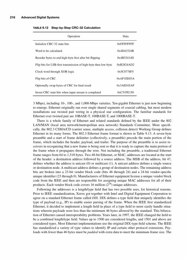
216 Advanced Digital Systems
3 Mbps), including 10-, 100-, and 1,000-Mbps varieties. Ten-gigabit Ethernet is just now beginningto emerge. Ethernet originally ran over single shared segments of coaxial cabling, but most moderninstallations use twisted pair wiring in a physical star configuration. The familiar standards forEthernet over twisted pair are 10BASE-T, 100BASE-T, and 1000BASE-T.
There is a whole family of Ethernet and related standards defined by the IEEE under the 802LAN/MAN (local area network/metropolitan area network) Standards Committee. More specifi-cally, the 802.3 CSMA/CD (carrier sense, multiple access, collision detect) Working Group definesEthernet in its many forms. The 802.3 Ethernet frame format is shown in Table 9.13. A seven-bytepreamble and a start of frame delimiter (collectively, a preamble) precede the main portion of theframe, which includes the header, payload, and trailer. The purpose of the preamble is to assist re-ceivers in recognizing that a new frame is being sent so that it is ready to capture the main portion ofthe frame when it propagates through the wire. Not including the preamble, a traditional Ethernetframe ranges from 64 to 1,518 bytes. Two 48-bit Ethernet, or MAC, addresses are located at the startof the header: a destination address followed by a source address. The MSB of the address, bit 47,defines whether the address is unicast (0) or multicast (1). A unicast address defines a single sourceor destination node. A multicast address defines a group of destination nodes. The remaining addressbits are broken into a 23-bit vendor block code (bits 46 through 24) and a 24-bit vendor-specificunique identifier (23 through 0). Manufacturers of Ethernet equipment license a unique vendor blockcode from the IEEE and then are responsible for assigning unique MAC addresses for all of theirproducts. Each vendor block code covers 16 million (224) unique addresses.
Following the addresses is a length/type field that has two possible uses, for historical reasons.Prior to IEEE standardization, Xerox got together with Intel and Digital Equipment Corporation toagree on a standard Ethernet frame called DIX. DIX defines a type field that uniquely identifies thetype of payload (e.g., IP) to enable easier parsing of the frame. When the IEEE first standardizedEthernet, it decided to implement a length field in place of a type field to more easily handle situa-tions wherein payloads were less than the minimum 46 bytes allowed by the standard. This bifurca-tion of Ethernet caused interoperability problems. Years later, in 1997, the IEEE changed the field tobe a combined length/type field. Values up to 1500 are considered lengths, and 1501 and above areconsidered types. Most Ethernet implementations use the original DIX-type field scheme. The IEEEhas standardized a variety of type values to identify IP and certain other protocol extensions. Pay-loads with fewer than 46 bytes must be padded with extra data to meet the minimum frame size. The
TABLE 9.12 Step-by-Step CRC-32 Calculation
Operation Data
Initialize CRC-32 state bits 0xFFFFFFFF
Word to be calculated 0x4D41524B
Reorder bytes to end high-byte first after bit-flipping 0x4B52414D
Flip bits for LSB-first transmission of high-byte then low-byte 0xB2824AD2
Clock word through XOR logic 0x5C0778F5
Flip bits of CRC 0xAF1EE03A
Optionally swap bytes of CRC for final result 0x3AE01EAF
Invert CRC state bits when input stream is completed 0xC51FE150
-Balch.book Page 216 Thursday, May 15, 2003 3:46 PM

Networking 217
resolution of how many real data bytes are actually in an Ethernet frame is typically handled byhigher-level protocols, such as IP, that contain their own length fields.
Modern Ethernet frames can be longer than 1,518 bytes for a couple of reasons. First, the IEEEhas defined various data fields that can be thought of as extensions to the traditional Ethernet header.These include VLAN (virtual LAN) and MPLS (multiprotocol label switching) tags. Each of theseextensions provides additional addressing and routing information for more advanced networkingdevices and adds length to the frame. Second, the industry began supporting jumbo frames in the late1990s to extend an Ethernet frame to 9 kB. The advantage of a jumbo frame is that the same amountof data can be transferred with fewer individual frames, reducing overhead. Jumbo frame support isnot universal, however. Older Ethernet equipment most likely will not handle such frames.
The frame check sequence is a 32-bit CRC that is computed across the entire main portion of theframe from the destination address through the last payload byte.
Because of its original topology as a shared bus, Ethernet employs a fairly simple yet effective ar-bitration mechanism to share access to the physical medium. This scheme is collision detection withrandom back-off, which was discussed earlier. Ethernet is referred to as CSMA/CD because of itsaccess sharing mechanism. Frame size plays a role in the operation of CSMA/CD. A minimumframe size is necessary to ensure that, for a given physical network size, all nodes are capable ofproperly detecting a collision in time to take the correct action. Electrical signals propagate throughcopper wire at a finite velocity. Therefore, if two nodes at opposite ends of a bus begin transmittingat the same time, it will take a finite time for each to recognize a collision. Once a frame is success-fully in progress, all other nodes must wait for that frame to end before they can transmit. A maxi-mum frame size limits the time that a single node can occupy the shared network. Additionally, amaximum frame size limits the buffer size within Ethernet MAC logic. In the 1970s and early 1980s,the cost of memory was so high as to justify relatively small maximum frame sizes. Today, this is nota significant concern in most products, hence the emergence of jumbo frames.
Even when Ethernet networks are deployed in physical star configurations, they are often con-nected to hubs that electrically merge the star segments into a single, logically shared medium. A tra-ditional Ethernet network is half-duplex, because only one frame can be in transit at any instant intime. Hubs are the least expensive way to connect several computers via Ethernet, because they dolittle more than merge star segments into a bus. Bus topologies present a fixed pool of bandwidththat must be shared by all nodes on that bus. As the number of nodes on a network increases, thetraffic load is likely to increase as well. Therefore, there is a practical limit on the size of a bussedEthernet network. Bridges were developed to mitigate Ethernet congestion problems by connecting
TABLE 9.13 IEEE 802.3 Ethernet Frame Format
Field Bytes Fixed Value
Preamble 7 0x55
Start of frame delimiter 1 0xD5
Destination address 6 No
Source address 6 No
Length/type 2 No
Payload data 46–1500 No
Frame check sequence (CRC) 4 No
-Balch.book Page 217 Thursday, May 15, 2003 3:46 PM

218 Advanced Digital Systems
multiple independent bus segments. A bridge operates at layer two using MAC addresses and buildsa database of which addresses are on which side of the bridge. Only traffic that must cross the bridgeto another segment is actually passed to the relevant segment. Otherwise, traffic can remain local ona single Ethernet segment without causing congestion on other segments. Bridging is illustrated inFig. 9.13. Nodes 1 and 7 can simultaneously send data within their local segments. Later, node 4 cansend data across the bridge to node 8, during which both network segments are burdened with thesingle transfer. The simplicity of this approach is that node 4 does not have any knowledge that node8 is on a different segment. Crossing between Ethernet segments is handled transparently by thebridge.
Layer-two switches take bridging a step farther by providing many independent Ethernet portsthat can exchange frames simultaneously without necessarily interfering with the traffic of otherports. As long as multiple ports are not trying to send data to the same destination port, those portscan all send data to different ports as if there existed many separate dedicated connections within theswitch. This is known as packet switching: instantaneous connections between ports are made andthen broken on a packet-by-packet basis. If two or more ports try to send data to the same port at thesame time, one port will be allowed to transmit, while the others will not. Ethernet was developed tobe a simple and inexpensive technology. Therefore, rather than providing special logic to handlesuch congestion issues, it was assumed that the network would generally have sufficient bandwidthto serve the application. During brief periods of high demand where not all data could be reliably de-livered, it was assumed that higher-level protocols (e.g., TCP/IP) would handle such special cases insoftware, thereby saving money in reducing hardware complexity at the expense of throughput. Tra-ditional Ethernet switches simply drop frames when congestion arises. In the case of switch conges-tion wherein multiple ports are sending data to a single port, all but one of those source ports mayhave their frames discarded. In reality, most switches contain a small amount of buffering that cantemporarily hold a small number of frames that would otherwise be discarded as a result of conges-tion. However, these buffers do not prevent frame drops when congestion rises above a certainthreshold. This behavior underscores the utility of layer-four protocols such as TCP.
Each switch port can conceivably be connected to a separate bused Ethernet segment and providebridging functions on a broader scale than older bridges with only two ports. Switching has trans-formed network architecture as the cost of hardware has dropped over the years. It is common tofind central computing resources such as file servers and printers with dedicated switch ports as
BridgeNode 1 Node 2 Node 3 Node 4
Node 5 Node 6 Node 7 Node 8
1
5
2
3
4
FIGURE 9.13 Ethernet bridging.
-Balch.book Page 218 Thursday, May 15, 2003 3:46 PM
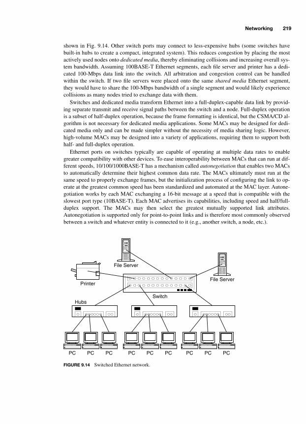
Networking 219
shown in Fig. 9.14. Other switch ports may connect to less-expensive hubs (some switches havebuilt-in hubs to create a compact, integrated system). This reduces congestion by placing the mostactively used nodes onto dedicated media, thereby eliminating collisions and increasing overall sys-tem bandwidth. Assuming 100BASE-T Ethernet segments, each file server and printer has a dedi-cated 100-Mbps data link into the switch. All arbitration and congestion control can be handledwithin the switch. If two file servers were placed onto the same shared media Ethernet segment,they would have to share the 100-Mbps bandwidth of a single segment and would likely experiencecollisions as many nodes tried to exchange data with them.
Switches and dedicated media transform Ethernet into a full-duplex-capable data link by provid-ing separate transmit and receive signal paths between the switch and a node. Full-duplex operationis a subset of half-duplex operation, because the frame formatting is identical, but the CSMA/CD al-gorithm is not necessary for dedicated media applications. Some MACs may be designed for dedi-cated media only and can be made simpler without the necessity of media sharing logic. However,high-volume MACs may be designed into a variety of applications, requiring them to support bothhalf- and full-duplex operation.
Ethernet ports on switches typically are capable of operating at multiple data rates to enablegreater compatibility with other devices. To ease interoperability between MACs that can run at dif-ferent speeds, 10/100/1000BASE-T has a mechanism called autonegotiation that enables two MACsto automatically determine their highest common data rate. The MACs ultimately must run at thesame speed to properly exchange frames, but the initialization process of configuring the link to op-erate at the greatest common speed has been standardized and automated at the MAC layer. Autone-gotiation works by each MAC exchanging a 16-bit message at a speed that is compatible with theslowest port type (10BASE-T). Each MAC advertises its capabilities, including speed and half/full-duplex support. The MACs may then select the greatest mutually supported link attributes.Autonegotiation is supported only for point-to-point links and is therefore most commonly observedbetween a switch and whatever entity is connected to it (e.g., another switch, a node, etc.).
File ServerPrinter
File Server
PC
Switch
PC PC PC PC PC PC PC PC
Hubs
FIGURE 9.14 Switched Ethernet network.
-Balch.book Page 219 Thursday, May 15, 2003 3:46 PM

This page intentionally left blank.

221
CHAPTER 10
Logic Design and Finite State Machines
A large component of digital systems design is the implementation of application-specific algo-rithms. In some cases, software implements the bulk of algorithms, because microprocessors areflexible and easily programmable for a wide range of functions. Such systems may use only hard-ware to acquire and store data on behalf of the software. Other systems may be unable to performtheir intended tasks with software alone. The reasons for this vary by application and often includethroughput requirements that are not practically achievable with a microprocessor.
When algorithms are implemented in hardware, state machines are often employed to accomplishthe task. A state machine can be made arbitrarily complex and can function similarly to softwarerunning on a microprocessor. Just as software moves through a sequence of tiny steps to solve alarger problem, a state machine can be designed to advance when certain conditions are satisfied. Asthe state machine progresses, it can activate other functions, just as software requests transactionsfrom a microprocessor’s peripherals.
This chapter focuses on higher-level logic design techniques used to implement functions rangingfrom basic microprocessor address decoding to clock domain crossing to state machines. Few designmethodologies are mandatory, but certain techniques make the design task easier by freeing an engi-neer from having to worry about mundane low-level details while concentrating on the higher-levelfunctions. Most software today is not written in assembly language, because the high-level languagemethodology is so productive. A software engineer does not have to worry about the accumulatorand addressing modes of a microprocessor and can concentrate on the specific application beingwritten. Likewise, more automated logic design techniques such as
hardware description languages
(HDL) handle the tasks of logic minimization and gate interconnection so that a hardware engineercan spend more time implementing the necessary algorithms for a specific application.
A great thing for the design community is that HDLs, once used by a relatively small set of com-panies with hefty financial resources, are becoming less expensive and more accessible with eachpassing year. The investment required to begin with these tools at the entry level ranges from nearlyfree up to a few thousand dollars, depending on the features desired and the subsidization that maybe available. Because of the wide popularity of HDLs, several companies that manufacture program-mable logic devices provide free or low-cost development tools to their customers. Stand-alone en-try-level HDL tools are also available from companies including Model Technology and Simucad.
10.1 HARDWARE DESCRIPTION LANGUAGES
Many basic peripheral logic functions are available in off-the-shelf ICs. A variety of UART ICs areavailable, DMA controllers are available, and simple address decoding can be accomplished with
-Balch.book Page 221 Thursday, May 15, 2003 3:46 PM
Copyright 2003 by The McGraw-Hill Companies, Inc. Click Here for Terms of Use.
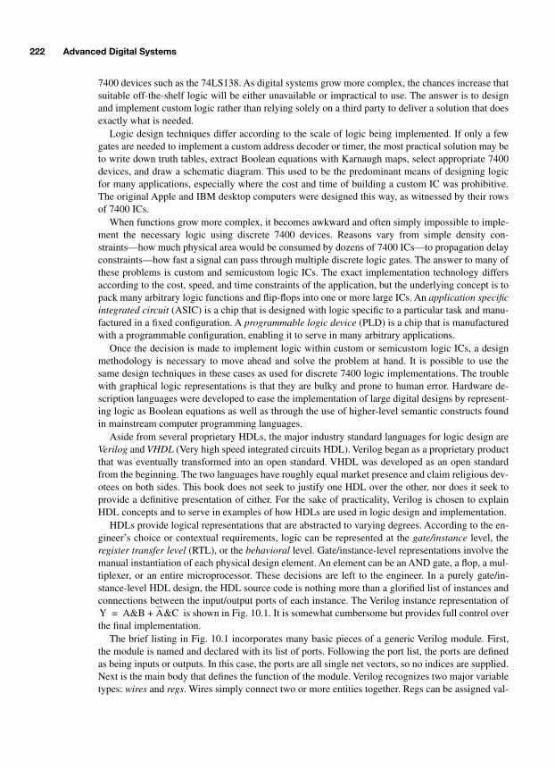
222 Advanced Digital Systems
7400 devices such as the 74LS138. As digital systems grow more complex, the chances increase thatsuitable off-the-shelf logic will be either unavailable or impractical to use. The answer is to designand implement custom logic rather than relying solely on a third party to deliver a solution that doesexactly what is needed.
Logic design techniques differ according to the scale of logic being implemented. If only a fewgates are needed to implement a custom address decoder or timer, the most practical solution may beto write down truth tables, extract Boolean equations with Karnaugh maps, select appropriate 7400devices, and draw a schematic diagram. This used to be the predominant means of designing logicfor many applications, especially where the cost and time of building a custom IC was prohibitive.The original Apple and IBM desktop computers were designed this way, as witnessed by their rowsof 7400 ICs.
When functions grow more complex, it becomes awkward and often simply impossible to imple-ment the necessary logic using discrete 7400 devices. Reasons vary from simple density con-straints—how much physical area would be consumed by dozens of 7400 ICs—to propagation delayconstraints—how fast a signal can pass through multiple discrete logic gates. The answer to many ofthese problems is custom and semicustom logic ICs. The exact implementation technology differsaccording to the cost, speed, and time constraints of the application, but the underlying concept is topack many arbitrary logic functions and flip-flops into one or more large ICs. An
application specificintegrated circuit
(ASIC) is a chip that is designed with logic specific to a particular task and manu-factured in a fixed configuration. A
programmable logic device
(PLD) is a chip that is manufacturedwith a programmable configuration, enabling it to serve in many arbitrary applications.
Once the decision is made to implement logic within custom or semicustom logic ICs, a designmethodology is necessary to move ahead and solve the problem at hand. It is possible to use thesame design techniques in these cases as used for discrete 7400 logic implementations. The troublewith graphical logic representations is that they are bulky and prone to human error. Hardware de-scription languages were developed to ease the implementation of large digital designs by represent-ing logic as Boolean equations as well as through the use of higher-level semantic constructs foundin mainstream computer programming languages.
Aside from several proprietary HDLs, the major industry standard languages for logic design are
Verilog
and
VHDL
(Very high speed integrated circuits HDL). Verilog began as a proprietary productthat was eventually transformed into an open standard. VHDL was developed as an open standardfrom the beginning. The two languages have roughly equal market presence and claim religious dev-otees on both sides. This book does not seek to justify one HDL over the other, nor does it seek toprovide a definitive presentation of either. For the sake of practicality, Verilog is chosen to explainHDL concepts and to serve in examples of how HDLs are used in logic design and implementation.
HDLs provide logical representations that are abstracted to varying degrees. According to the en-gineer’s choice or contextual requirements, logic can be represented at the
gate/instance
level, the
register transfer level
(RTL), or the
behavioral
level. Gate/instance-level representations involve themanual instantiation of each physical design element. An element can be an AND gate, a flop, a mul-tiplexer, or an entire microprocessor. These decisions are left to the engineer. In a purely gate/in-stance-level HDL design, the HDL source code is nothing more than a glorified list of instances andconnections between the input/output ports of each instance. The Verilog instance representation of
is shown in Fig. 10.1. It is somewhat cumbersome but provides full control overthe final implementation.
The brief listing in Fig. 10.1 incorporates many basic pieces of a generic Verilog module. First,the module is named and declared with its list of ports. Following the port list, the ports are definedas being inputs or outputs. In this case, the ports are all single net vectors, so no indices are supplied.Next is the main body that defines the function of the module. Verilog recognizes two major variabletypes:
wires
and
regs
. Wires simply connect two or more entities together. Regs can be assigned val-
Y A&B A&C+=
-Balch.book Page 222 Thursday, May 15, 2003 3:46 PM
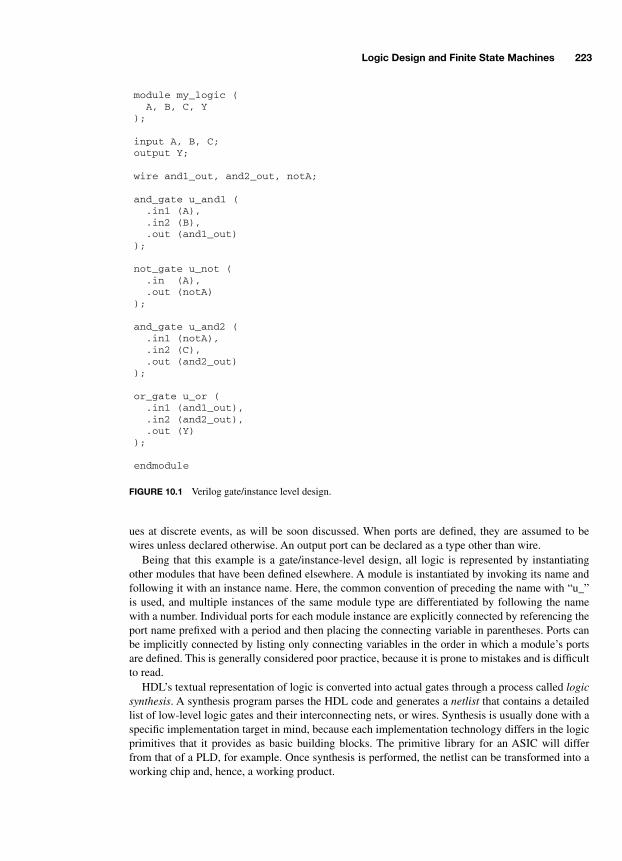
Logic Design and Finite State Machines 223
ues at discrete events, as will be soon discussed. When ports are defined, they are assumed to bewires unless declared otherwise. An output port can be declared as a type other than wire.
Being that this example is a gate/instance-level design, all logic is represented by instantiatingother modules that have been defined elsewhere. A module is instantiated by invoking its name andfollowing it with an instance name. Here, the common convention of preceding the name with “u_”is used, and multiple instances of the same module type are differentiated by following the namewith a number. Individual ports for each module instance are explicitly connected by referencing theport name prefixed with a period and then placing the connecting variable in parentheses. Ports canbe implicitly connected by listing only connecting variables in the order in which a module’s portsare defined. This is generally considered poor practice, because it is prone to mistakes and is difficultto read.
HDL’s textual representation of logic is converted into actual gates through a process called
logicsynthesis
. A synthesis program parses the HDL code and generates a
netlist
that contains a detailedlist of low-level logic gates and their interconnecting nets, or wires. Synthesis is usually done with aspecific implementation target in mind, because each implementation technology differs in the logicprimitives that it provides as basic building blocks. The primitive library for an ASIC will differfrom that of a PLD, for example. Once synthesis is performed, the netlist can be transformed into aworking chip and, hence, a working product.
module my_logic ( A, B, C, Y ); input A, B, C; output Y; wire and1_out, and2_out, notA; and_gate u_and1 ( .in1 (A), .in2 (B), .out (and1_out) ); not_gate u_not ( .in (A), .out (notA) ); and_gate u_and2 ( .in1 (notA), .in2 (C), .out (and2_out) ); or_gate u_or ( .in1 (and1_out), .in2 (and2_out), .out (Y) ); endmodule
FIGURE 10.1 Verilog gate/instance level design.
-Balch.book Page 223 Thursday, May 15, 2003 3:46 PM
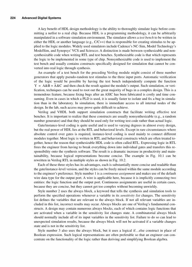
224 Advanced Digital Systems
A key benefit of HDL design methodology is the ability to thoroughly simulate logic before com-mitting a netlist to a real chip. Because HDL is a programming methodology, it can be arbitrarilymanipulated in a software simulation environment. The simulator allows a
test bench
to be written ineither the HDL or another language (e.g., C/C++) that is responsible for creating stimulus to be ap-plied to the logic modules. Widely used simulators include Cadence’s NC-Sim, Model Technology’sModelSim, and Synopsys’ VCS and Scirocco. A distinction is made between synthesizable and non-synthesizable code when writing RTL and test benches. Synthesizable code is that which representsthe logic to be implemented in some type of chip. Nonsynthesizable code is used to implement thetest bench and usually contains constructs specifically designed for simulation that cannot be con-verted into real logic through synthesis.
An example of a test bench for the preceding Verilog module might consist of three numbergenerators that apply pseudo-random test stimulus to the three input ports. Automatic verificationof the logic would be possible by having the test bench independently compute the function
and then check the result against the module’s output. Such simulation, or veri-fication, techniques can be used to root out the great majority of bugs in a complex design. This is atremendous feature, because fixing bugs after an ASIC has been fabricated is costly and time con-suming. Even in cases in which a PLD is used, it is usually faster to isolate and fix a bug in simula-tion than in the laboratory. In simulation, there is immediate access to all internal nodes of thedesign. In the lab, such access may prove quite difficult to achieve.
Verilog and VHDL both support simulation constructs that facilitate writing effective testbenches. It is important to realize that these constructs are usually nonsynthesizable (e.g., a randomnumber generator) and that they should be used only for writing test code rather than actual logic.
Gate/instance-level coding is quite useful and is used to varying degrees in almost every design,but the real power of HDL lies at the RTL and behavioral levels. Except in rare circumstances whereabsolute control over gates is required, instance-level coding is used mainly to connect differentmodules together. Most logic is written in RTL and behavioral constructs which are often treated to-gether, hence the reason that synthesizable HDL code is often called RTL. Expressing logic in RTLfrees the engineer from having to break everything down into individual gates and transfers this re-sponsibility onto the synthesis software. The result is a dramatic increase in productivity and main-tainability, because logical representations become concise. The example in Fig. 10.1 can berewritten in Verilog RTL in multiple styles as shown in Fig. 10.2.
Each of these three styles has its advantages, each is substantially more concise and readable thanthe gate/instance-level version, and the styles can be freely mixed within the same module accordingto the engineer’s preference. Style number 1 is a
continuous assignment
and makes use of the defaultwire data type for the output port. A wire is applicable here, because it is implicitly connecting twoentities: the logic function and the output port. Continuous assignments are useful in certain cases,because they are concise, but they cannot get too complex without becoming unwieldy.
Style number 2 uses the always block, a keyword that tells the synthesis and simulation tools toperform the specified operations whenever a variable in its
sensitivity list
changes. The sensitivitylist defines the variables that are relevant to the always block. If not all relevant variables are in-cluded in this list, incorrect results may occur. Always blocks are one of Verilog’s fundamental con-structs. A design may contain numerous always blocks, each of which contains logic functions thatare activated when a variable in the sensitivity list changes state. A combinatorial always blockshould normally include all of its input variables in the sensitivity list. Failure to do so can lead tounexpected simulation results, because the always block will not be activated if a variable changesstate and is not in the sensitivity list.
Style number 3 also uses the always block, but it uses a logical if…else construct in place ofBoolean expression. Such logical representations are often preferable so that an engineer can con-centrate on the functionality of the logic rather than deriving and simplifying Boolean algebra.
Y A&B A&C+=
-Balch.book Page 224 Thursday, May 15, 2003 3:46 PM

Logic Design and Finite State Machines 225
The two examples shown thus far illustrate basic Verilog HDL syntax with combinatorial logic.Clearly, synchronous logic is critical to digital systems, and it is fully supported by HDLs. D-typeflip-flops are most commonly used in digital logic design, and they are directly inferred by using thecorrect RTL syntax. As always, gate-level instances of flops can be invoked, but this is discouragedfor the reasons already discussed. Figure 10.3 shows the Verilog RTL representation of two flops,one with a synchronous reset and the other with an asynchronous reset.
The first syntactical difference to notice is the Verilog keyword
posedge
. Posedge and its comple-ment,
negedge
, modify a sensitivity list variable to activate the always block only when it transitions.Synthesis tools are smart enough to recognize these keywords and infer a clocked flop. Clocked al-ways blocks should not include normal regs or wires in the sensitivity list, because it is only desiredto activate the block on the active clock edge or when an optional asynchronous reset transitions.
At reset, a default 0 value is assigned to Q. Constants in Verilog can be explicitly sized and refer-enced to a particular radix. Preceding a constant with `b denotes it as binary (`h is hex, and `d is dec-imal). Preceding the radix identifier with a number indicates the number of bits occupied by thatconstant.
Another syntactical difference to note is the use of a different type of assignment operator: <= in-stead of =. This is known as a non-blocking (<=) assignment as compared to a blocking (=) assign-ment. It is considered good practice to use non-blocking assignments when inferring flops, because
module my_logic ( A, B, C, Y ); input A, B, C; output Y; // Style #1: continuous assignment assign Y = (A && B) || (!A && C);
// Style #2: behavioral assignment reg Y; always @(A or B or C) begin Y = (A && B) || (!A && C); end // Style #3: if...then construct reg Y; always @(A or B or C) begin if (A) Y = B; else Y = C; end endmodule
FIGURE 10.2 Verilog RTL-level design.
-Balch.book Page 225 Thursday, May 15, 2003 3:46 PM
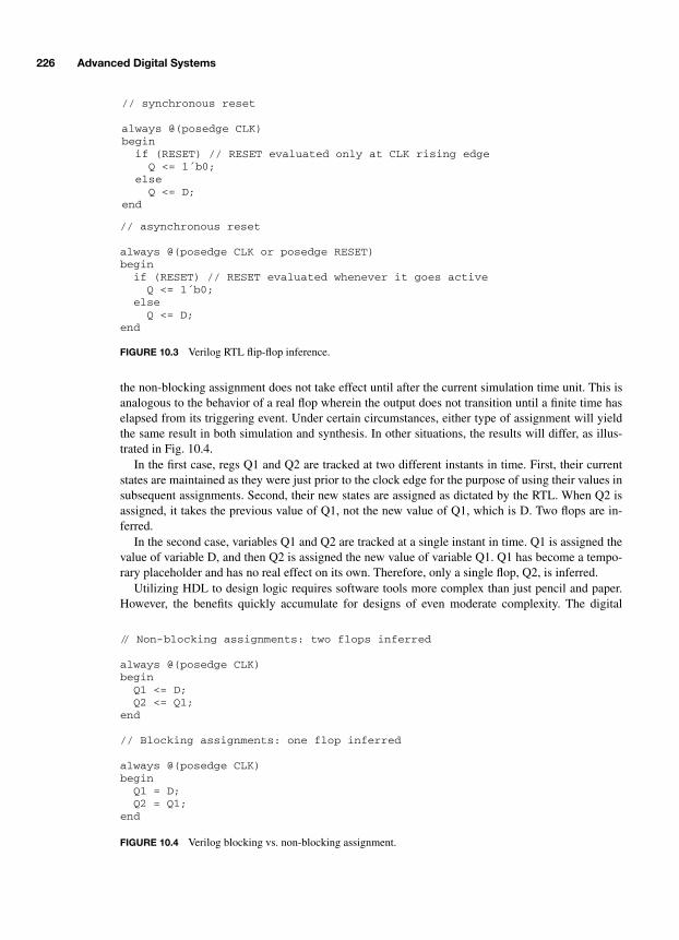
226 Advanced Digital Systems
the non-blocking assignment does not take effect until after the current simulation time unit. This isanalogous to the behavior of a real flop wherein the output does not transition until a finite time haselapsed from its triggering event. Under certain circumstances, either type of assignment will yieldthe same result in both simulation and synthesis. In other situations, the results will differ, as illus-trated in Fig. 10.4.
In the first case, regs Q1 and Q2 are tracked at two different instants in time. First, their currentstates are maintained as they were just prior to the clock edge for the purpose of using their values insubsequent assignments. Second, their new states are assigned as dictated by the RTL. When Q2 isassigned, it takes the previous value of Q1, not the new value of Q1, which is D. Two flops are in-ferred.
In the second case, variables Q1 and Q2 are tracked at a single instant in time. Q1 is assigned thevalue of variable D, and then Q2 is assigned the new value of variable Q1. Q1 has become a tempo-rary placeholder and has no real effect on its own. Therefore, only a single flop, Q2, is inferred.
Utilizing HDL to design logic requires software tools more complex than just pencil and paper.However, the benefits quickly accumulate for designs of even moderate complexity. The digital
// synchronous reset always @(posedge CLK) begin if (RESET) // RESET evaluated only at CLK rising edge Q <= 1´b0; else Q <= D; end
// asynchronous reset always @(posedge CLK or posedge RESET) begin if (RESET) // RESET evaluated whenever it goes active Q <= 1´b0; else Q <= D; end
FIGURE 10.3 Verilog RTL flip-flop inference.
// Non-blocking assignments: two flops inferred always @(posedge CLK) begin Q1 <= D; Q2 <= Q1; end // Blocking assignments: one flop inferred always @(posedge CLK) begin Q1 = D; Q2 = Q1; end
FIGURE 10.4 Verilog blocking vs. non-blocking assignment.
-Balch.book Page 226 Thursday, May 15, 2003 3:46 PM

Logic Design and Finite State Machines 227
functions and techniques discussed in the remainder of this chapter show how practical HDL designcan be.
10.2 CPU SUPPORT LOGIC
Most digital systems require some quantity of miscellaneous glue logic to help tie a CPU to itsmemory and I/O peripherals. Some of the most common support functions are address decoding,basic I/O signals, interrupt control, and timers. Another common function is interface conversionwhereby the CPU needs to talk with a peripheral that has an interface that is incompatible with thatof the CPU. Interface conversion can range from simple control signal polarity adjustments to com-plex buffering schemes that cross clock domains with FIFOs.
Address decoding is usually a combinatorial implementation, because many CPU interfaces arenonpipelined. When performing address decoding and other bus control functions for a pipelinedCPU bus, a more complex synchronous circuit is called for that can track the various pipeline stagesand take the necessary actions during each stage. Basic combinatorial address decoding consists ofmapping ranges of addresses to chip selects. Chip select signals are usually active-low by conventionand are numbered upward from 0. For the sake of discussion, consider the 24-bit memory map in Ta-ble 10.1 to design an address decoder.
Four external chip selects are called out. Instead of using the asterisk to denote active-low signals,the underscore is used, because an asterisk is not a valid character for use in a Verilog identifier. Thefirst two chip selects are used for ROM (e.g., flash or EPROM) and their memory ranges are swappa-ble according to the RomSel signal. It is sometimes useful to provide an alternate boot ROM that canbe installed at a later date for various purposes such as a software upgrade. When boot ROM is im-plemented in flash, the CPU is able to load new data into its ROM. If there is no other way to send anew software image to the system, the image can be loaded onto a ROM module that is temporarily
TABLE
10.1 Example Memory Map
Address Range Qualifier Chip Select Function
0x000000–0x0FFFFF RomSel=0CS0_ 1-MB default boot ROM
0x100000–0x1FFFFF RomSel=1
0x100000–0x1FFFFF RomSel=0CS1_ 1-MB ROM module
0x000000–0x0FFFFF RomSel=1
0x200000–0x21FFFF N/A CS2_ 128-kB SRAM
0x220000–0x2FFFFF N/A None Unused
0x300000–0x30000F N/A CS3_ UART
0x300010–0x3FFFFF N/A None Unused
0x400000–0x4FFFFF N/A Internal Control/status registers
0x500000–0xFFFFFF N/A None Unused
-Balch.book Page 227 Thursday, May 15, 2003 3:46 PM
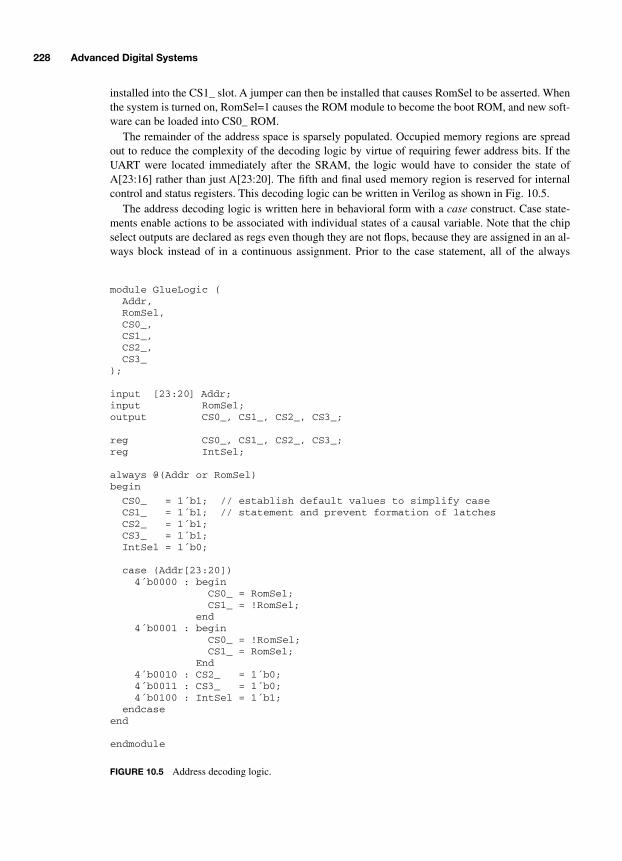
228 Advanced Digital Systems
installed into the CS1_ slot. A jumper can then be installed that causes RomSel to be asserted. Whenthe system is turned on, RomSel=1 causes the ROM module to become the boot ROM, and new soft-ware can be loaded into CS0_ ROM.
The remainder of the address space is sparsely populated. Occupied memory regions are spreadout to reduce the complexity of the decoding logic by virtue of requiring fewer address bits. If theUART were located immediately after the SRAM, the logic would have to consider the state ofA[23:16] rather than just A[23:20]. The fifth and final used memory region is reserved for internalcontrol and status registers. This decoding logic can be written in Verilog as shown in Fig. 10.5.
The address decoding logic is written here in behavioral form with a
case
construct. Case state-ments enable actions to be associated with individual states of a causal variable. Note that the chipselect outputs are declared as regs even though they are not flops, because they are assigned in an al-ways block instead of in a continuous assignment. Prior to the case statement, all of the always
module GlueLogic ( Addr, RomSel, CS0_, CS1_, CS2_, CS3_ ); input [23:20] Addr; input RomSel; output CS0_, CS1_, CS2_, CS3_; reg CS0_, CS1_, CS2_, CS3_; reg IntSel; always @(Addr or RomSel) begin
CS0_ = 1´b1; // establish default values to simplify case CS1_ = 1´b1; // statement and prevent formation of latches CS2_ = 1´b1; CS3_ = 1´b1; IntSel = 1´b0; case (Addr[23:20]) 4´b0000 : begin CS0_ = RomSel; CS1_ = !RomSel; end 4´b0001 : begin CS0_ = !RomSel; CS1_ = RomSel; End 4´b0010 : CS2_ = 1´b0; 4´b0011 : CS3_ = 1´b0; 4´b0100 : IntSel = 1´b1; endcase end endmodule
FIGURE 10.5 Address decoding logic.
-Balch.book Page 228 Thursday, May 15, 2003 3:46 PM
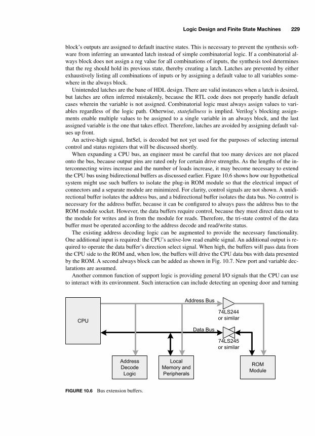
Logic Design and Finite State Machines 229
block’s outputs are assigned to default inactive states. This is necessary to prevent the synthesis soft-ware from inferring an unwanted latch instead of simple combinatorial logic. If a combinatorial al-ways block does not assign a reg value for all combinations of inputs, the synthesis tool determinesthat the reg should hold its previous state, thereby creating a latch. Latches are prevented by eitherexhaustively listing all combinations of inputs or by assigning a default value to all variables some-where in the always block.
Unintended latches are the bane of HDL design. There are valid instances when a latch is desired,but latches are often inferred mistakenly, because the RTL code does not properly handle defaultcases wherein the variable is not assigned. Combinatorial logic must always assign values to vari-ables regardless of the logic path. Otherwise,
statefullness
is implied. Verilog’s blocking assign-ments enable multiple values to be assigned to a single variable in an always block, and the lastassigned variable is the one that takes effect. Therefore, latches are avoided by assigning default val-ues up front.
An active-high signal, IntSel, is decoded but not yet used for the purposes of selecting internalcontrol and status registers that will be discussed shortly.
When expanding a CPU bus, an engineer must be careful that too many devices are not placedonto the bus, because output pins are rated only for certain drive strengths. As the lengths of the in-terconnecting wires increase and the number of loads increase, it may become necessary to extendthe CPU bus using bidirectional buffers as discussed earlier. Figure 10.6 shows how our hypotheticalsystem might use such buffers to isolate the plug-in ROM module so that the electrical impact ofconnectors and a separate module are minimized. For clarity, control signals are not shown. A unidi-rectional buffer isolates the address bus, and a bidirectional buffer isolates the data bus. No control isnecessary for the address buffer, because it can be configured to always pass the address bus to theROM module socket. However, the data buffers require control, because they must direct data out tothe module for writes and in from the module for reads. Therefore, the tri-state control of the databuffer must be operated according to the address decode and read/write status.
The existing address decoding logic can be augmented to provide the necessary functionality.One additional input is required: the CPU’s active-low read enable signal. An additional output is re-quired to operate the data buffer’s direction select signal. When high, the buffers will pass data fromthe CPU side to the ROM and, when low, the buffers will drive the CPU data bus with data presentedby the ROM. A second always block can be added as shown in Fig. 10.7. New port and variable dec-larations are assumed.
Another common function of support logic is providing general I/O signals that the CPU can useto interact with its environment. Such interaction can include detecting an opening door and turning
Address Bus
CPU
Address
Decode
Logic
Local
Memory and
Peripherals
ROM
Module
74LS244
or similar
74LS245
or similar
Data Bus
FIGURE 10.6 Bus extension buffers.
-Balch.book Page 229 Thursday, May 15, 2003 3:46 PM

230 Advanced Digital Systems
on an alarm. The opening door can be detected using a switch connected to an input signal. Whenthe CPU reads the status of this signal, it can determine whether the switch is open or closed. Analarm can be turned on when the CPU sets an output signal that enables an alarm circuit. Control andstatus registers must be implemented to enable the CPU to read and write I/O signals. In our continu-ing example, we assume an eight-bit data bus coming from the CPU and the need for eight input sig-nals and eight output signals. Implementing registers varies according to whether the CPU bus issynchronous or asynchronous. Some older microprocessors use asynchronous buses requiringlatches to be formed within the support logic. Figure 10.8 shows the implementation of two registersusing the previously decoded IntSel signal in both synchronous and asynchronous styles. Again, theproper declarations for ports and variables are assumed.
An added level of address decoding is required here to ensure that the two registers are not ac-cessed simultaneously. The register logic consists of two basic sections: the write logic and readlogic. The write logic (required only for the control register that drives output signals) transfers thecontents of the CPU data bus to the internal register when the register is addressed and the write en-able is active. The ControlRegSel signal is implemented in a case statement but can be implementedin a variety of ways. More select signals will be added in coming examples. The asynchronous writelogic infers a latch, because not all permutations of input qualifiers are represented by assignments.If Reset_ is high and the control register is not being selected for a write, there is no specified action.Therefore, memory is implied and, in the absence of a causal clock, a latch is inferred. The synchro-nous write logic is almost identical, but it references a clock that causes a flop inference. Reset is im-plemented to provide a known initial state. This is a good idea so that external logic that is driven bythe control register can be safely designed with the assumption that operations begin at a knownstate. The known state is usually inactive so that peripherals do not start operating before the CPUfinishes booting and can disable them.
The read logic consists of two sections: the output multiplexer and the output buffer control. Theoutput multiplexer simply selects one of the available registers for reading. It is not necessary toqualify the multiplexer with any other logic, because a read will not actually take place unless theoutput buffer control logic sends the data to the CPU. Rather than preventing a latch in ReadData
byassigning it a default value before the case construct, the Verilog keyword
default
is used as the finalcase enumeration to specify default operation. Either solution will work—it is a matter of preferenceand style over which to use in a given situation. Both read-only and writable registers are included inthe read multiplexer logic. Strictly speaking, it is not mandatory to have writable register contentsreadable by the CPU, but this is a very good practice. Years ago, when logic was very expensive, itwas not uncommon to find write-only registers. However, there is a substantial drawback to this ap-proach: you can never be sure what the contents of the register are if you fail to keep track of the ex-act data that has already been written!
Implementing bidirectional signals in Verilog can be done with a continuous assignment that se-lects between driving an active variable or a high-impedance value, Z. The asynchronous read logicis very simple: whenever the internal registers are selected and read enable is active, the tri-statebuffer is enabled, and the output of the multiplexer is driven onto the CPU data bus. At all other
always @(CS1_ or Rd_) begin if (!CS1_ && !Rd_) DataBufDir = 1’b0; // drive CPU bus when ROM selected for read else DataBufDir = 1’b1; // otherwise, always drive data to ROM end
FIGURE 10.7 Data buffer control logic.
-Balch.book Page 230 Thursday, May 15, 2003 3:46 PM

Logic Design and Finite State Machines 231
always @(Addr[3:0] or StatusInput[7:0] or ControlReg[7:0] or IntSel) begin case (Addr[3:0]) // read multiplexer 4´h0 : ReadData[7:0] = StatusInput[7:0]; // external input pins 4´h1 : ReadData[7:0] = ControlReg[7:0]; default : ReadData[7:0] = 8´h0; // alternate means to prevent latch endcase ControlRegSel = 1´b0; // default inactive value case (Addr[3:0]) // select signal only needed for writeable registers 4´h1 : ControlRegSel = IntSel; endcase end // Option #1A: asynchronous read logic assign CpuData[7:0] = (IntSel && !Rd_) ? ReadData[7:0] : 8´bz; // Option #1B: synchronous read logic always @(posedge CpuClk) begin if (!Reset_) // synchronous reset CpuDataOE <= 1´b0; // no need to reset ReadDataReg and possibly save some logic else begin CpuDataOE <= IntSel && !Rd_; // all outputs are registered ReadDataReg[7:0] <= ReadData[7:0]; end end assign CpuData[7:0] = CpuDataOE ? ReadDataReg[7:0] : 8´bz; // Option #2A: asynchronous write logic always @(ControlRegSel or CpuData[7:0] or Wr_ or Reset_) begin if (!Reset_) ControlReg[7:0] = 8´h0; // reset state is cleared else if (ControlRegSel && !Wr_) ControlReg[7:0] = CpuData[7:0]; // missing else forces memory element: intentional latch! end // Option #2B: synchronous write logic always @(posedge CpuClk) begin if (!Reset_) // synchronous reset ControlReg[7:0] <= 8´h0; else if (ControlRegSel && !Wr_) ControlReg[7:0] <= CpuData[7:0]; end
FIGURE 10.8 Control/status register logic.
-Balch.book Page 231 Thursday, May 15, 2003 3:46 PM
232 Advanced Digital Systems
times, the data bus is held in a high-impedance state. This works as expected, because the value Zcan be overridden by another assignment. In simulation, the other assignment may come from a testbench that emulates the CPU’s operation. In synthesis, the software properly recognizes this ar-rangement as inferring a tri-state bus. The continuous assignment takes advantage of Verilog’s con-ditional operator, ? : , which serves an if…else function. When the logical expression before thequestion mark is true, the value before the colon is used. Otherwise, the value after the colon is used.A bidirectional port is declared using the Verilog
inout
keyword in place of
input
or
output
. The syn-chronous version of the read logic is very similar to the asynchronous version, except that the out-puts are first registered before being used in the tri-state assignment.
Interrupt control registers are implemented by support logic when the number of total interruptsources in the system exceeds the CPU’s interrupt handling capacity. Gathering multiple interruptsand presenting them to the CPU as a single interrupt signal can be as simple as logically ORing mul-tiple interrupt signals together. A somewhat more complex scheme, but one with value, is where in-terrupts can be selectively masked by the CPU, and system-wide interrupt status is accumulated in asingle register. This gives the CPU more control over how it gets interrupted and, when interrupted,provides a single register that can be read to determine the source of the interrupt. Such a schemecan be implemented with two registers and associated logic: a read/write interrupt mask register anda read-only interrupt status register. Each pair of bits in the mask and status registers corresponds toa single interrupt source. When an interrupt is active, the corresponding bit in the status register isactive. However, only those interrupt sources whose mask bits have been cleared will result in aCPU interrupt. At reset, the mask register defaults to 0xFF to disable all interrupts. Figure 10.9shows a Verilog implementation of interrupt control as an extension of the previous example. Syn-chronous registers are assumed here, but asynchronous logic is easily adapted.
Aside from the registers themselves, the main function of the interrupt control logic is imple-mented by the bit-wise ORing and reduction AND of the interrupt mask bits and the external inter-rupt signals. Verilog’s | operator is a bit-wise OR function in contrast to the || logical OR function.When two equal-size vectors are bit-wise ORed, the result is a single vector of the same size whereineach bit is the OR of the corresponding pair of bits of the operands. This first step disables any activeinterrupts that are masked; per DeMorgan’s law, an OR acts as an active-low AND function. The sec-ond step is a reduction AND as indicated by the unary & operator. Similar to OR, & is the bit-wiseversion of &&. Invoking & with a single operand makes it a reduction operator that ANDs togetherall bits of a vector and generates a single output bit. AND is used because the interrupt polarities areactive-low. Therefore, if any one interrupt is asserted (low), the reduction AND function will gener-ate a low output. Per DeMorgan’s law once again, an AND acts as an active-low OR function.
Timers are often useful structures that can periodically interrupt the CPU to invoke a time-criticalinterrupt service routine, enable the CPU to determine elapsed time, or trigger some other event inhardware. It is common to find timers implemented in certain CPU products such as microcontrol-lers. Sometimes, however, it becomes necessary to implement a custom timer in support logic. Onesuch example is presented here with a fixed prescaler and an eight-bit counter with an eight-bit con-figurable terminal count value. The prescaler is used to slow down the timer so that it can interruptthe CPU over longer periods of time. For the sake of discussion, let’s assume that the CPU is runningat a frequency of 10 MHz and that the timer granularity should be 1 ms. Therefore, the prescalershould count from 0 to 9,999 to generate a 1-ms tick when running with a 100-ns period. A Verilogimplementation of such a timer is shown in Fig. 10.10 without the associated read/write logic al-ready presented in detail. A 14-bit prescaler is necessary to represent numbers from 0 to 9,999. It isassumed that the terminal count register, TermCount, is implemented elsewhere as a general read/write register.
When the timer rolls over, it asserts TimerRollOver for one CpuClk cycle to trigger whateverlogic is desired by the application. If the trigger event is a CPU interrupt, the logic should create a
-Balch.book Page 232 Thursday, May 15, 2003 3:46 PM

Logic Design and Finite State Machines 233
“sticky” version of TimerRollOver that does not automatically get cleared by hardware. Rather, it issticky because, once set by hardware, the bit will retain its state until explicitly cleared by software.This provides an arbitrarily long time for software to respond to the interrupt assertion, read the in-terrupt status register to detect the timer roll-over event, and then clear the sticky bit. Without thesticky bit, software would have no chance of catching a pulse that is only a single cycle in width.
10.3 CLOCK DOMAIN CROSSING
Some logic design tasks involve exchanging information between logic running on unrelated clocks.When multiple independent clock domains exist in a system, there is no guaranteed skew or phaserelationship between the various clocks. Synchronous timing analysis dictates that a flop’s setup andhold times must be met to ensure reliable capture of the data presented to it. Yet it is impossible toguarantee proper setup and hold times when the source flop’s clock has no relationship to the desti-nation flop’s clock.
always @(Addr[3:0] or StatusInput[7:0] or ControlReg[7:0] or IntSel or ISR[7:0] or IMR[7:0]) begin case (Addr[3:0]) // read multiplexer 4´h0 : ReadData[7:0] = StatusInput[7:0]; // external input pins 4´h1 : ReadData[7:0] = ControlReg[7:0]; 4´h2 : ReadData[7:0] = ISR[7:0]; // interrupt status 4´h3 : ReadData[7:0] = IMR[7:0]; // interrupt mask default : ReadData[7:0] = 8´h0; // alternate means to prevent latch endcase
ControlRegSel = 1´b0; // default inactive value IMRSel = 1´b0;
case (Addr[3:0]) // select signal only needed for writeable registers 4´h1 : ControlRegSel = IntSel; 4´h3 : IMRSel = IntSel; endcase
end
// Interrupt gathering
always @(IMR[7:0] or ExtInt_[7:0]) begin ISR[7:0] = ExtInt_[7:0]; // reflect status of external signals CpuInt_ = &(IMR[7:0] | ExtInt_[7:0]); // reduction AND
end
// Write logic
always @(posedge CpuClk) begin if (!Reset_) IMR[7:0] <= 8´hff; // mask all interrupts on reset else if (IMRSel && !Wr_) IMR[7:0] <= CpuData[7:0];
end
FIGURE 10.9 Interrupt control logic.
-Balch.book Page 233 Thursday, May 15, 2003 3:46 PM

234 Advanced Digital Systems
There are several scenarios that arise from clocking a flop input with unknown timing as shown inFig. 10.11. First, there is a chance that the applied signal will be captured successfully if it happensto meet the flop’s setup time specification. Second, there is a chance that the input data will bemissed on the first clock cycle, because it occurs too late for the flop to detect it. If the data remainsasserted through the next cycle, it will be properly captured at that time.
Finally, there is a questionable area between capturing and missing the signal. A flop is inherentlyan analog circuit, because it is built from transistors. Flops behave digitally when their timing speci-fications are adhered to. When timing violations occur, the flop circuit may behave in a nondigitalmanner and generate a marginal output that is somewhere between 1 and 0 before eventually settlingto a valid logic state. It is not certain into which logic state the flop will settle, nor is it certain exactlyhow much time the flop will take to settle. This phenomenon is known as
metastability
. A flop is saidto be metastable when a timing violation occurs and it takes some time for the output to stabilize.Metastability does not damage the flop, but it can cause significant trouble for a synchronous circuitthat is designed with the assumption of predictable timing.
Clock domains can be reliably crossed when proper design techniques are used to accommodatelikely timing violations. Some applications require that only control signals move between clock do-mains, and others must transport entire data paths. The simpler case of individual control signals ispresented first and then used as a foundation for data paths.
Because it is impossible to avoid metastability when crossing clock domains, the phenomenonmust be managed. A control signal ostensibly triggers activity in the logic that it drives, and this des-tination logic waits for the control signal to transition. Metastability does not prevent the signal fromreaching its destination; it introduces uncertainty over exactly when the signal will stabilize in thedestination clock domain. This uncertainty is dealt with by
synchronizing
the control signal usingextra flops prior to treating the signal as a legal synchronous input. A two-stage synchronizing cir-cuit is shown in Fig. 10.12. The synchronizing circuit takes advantage of the high probability that ametastable flop’s output will achieve a stable digital state within a single clock cycle. If the firstflop’s output is stable, the second flop’s output will transition perfectly and present a signal with
always @(posedge CpuClk) begin if (!Reset_) begin Prescaler[13:0] <= 14´h0; Timer[7:0] <= 8´h0; TimerRollOver <= 1´b0; end else if (Prescaler[13:0] == 14´d9999) begin Prescaler[13:0] <= 14´h0; // roll-back to zero if (Timer[7:0] == TermCount[7:0]) begin Timer[7:0] <= 8´h0; // start over TimerRollOver <= 1´b1; // trigger other logic end else Timer[7:0] <= Timer[7:0] + 1; end else begin Prescaler[13:0] <= Prescaler[13:0] + 1; TimerRollOver <= 1´b0; end end
FIGURE 10.10 Timer logic.
-Balch.book Page 234 Thursday, May 15, 2003 3:46 PM

Logic Design and Finite State Machines 235
valid timing to the internal logic. If the first flop’s output is not yet stable, chances are that it will bevery close to a valid logic level, which generally should cause the second flop’s output to transitioncleanly. To deal with metastablility is to deal with probability. As the number of synchronizing flopsis increased, the probability of a metastable state reaching the internal logic rapidly approaches zero.A general rule of thumb is that two flops reduce the probability of metastability in internal logic topractically zero.
An unavoidable downside of synchronizing flops is that they add latency to a transaction, becausethe internal logic will not detect an asynchronous signal’s transition for two to three clock cycles af-ter it actually transitions (when using a two-flop synchronizer). The best-case scenario of two cyclesoccurs when the input signal happens to transition early enough to meet the first flop’s setup andhold timing. If these constraints are not met because the input signal transitions too late, the flop’s
Setup and hold window
Clock
Flop Input
Flop Output
Case #1: Flop's setup time is met
Clock
Flop Input
Flop Output
Case #2: Signal transitions after timing window
Clock
Flop Input
Flop Output
Case #3: Signal transitions within timing window(metastability)
FIGURE 10.11 Flop operation with variable input timing.
D Q D QClean timing
to internallogic
Asynchronousinput signal
Internal operating clock
FIGURE 10.12 Synchronizing flip-flop scheme.
-Balch.book Page 235 Thursday, May 15, 2003 3:46 PM
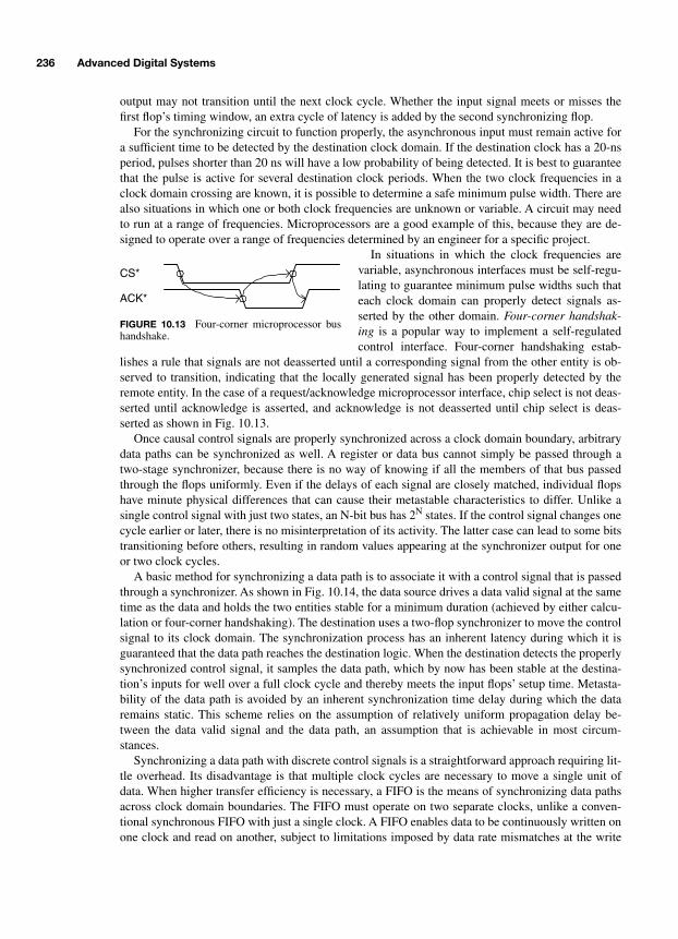
236 Advanced Digital Systems
output may not transition until the next clock cycle. Whether the input signal meets or misses thefirst flop’s timing window, an extra cycle of latency is added by the second synchronizing flop.
For the synchronizing circuit to function properly, the asynchronous input must remain active fora sufficient time to be detected by the destination clock domain. If the destination clock has a 20-nsperiod, pulses shorter than 20 ns will have a low probability of being detected. It is best to guaranteethat the pulse is active for several destination clock periods. When the two clock frequencies in aclock domain crossing are known, it is possible to determine a safe minimum pulse width. There arealso situations in which one or both clock frequencies are unknown or variable. A circuit may needto run at a range of frequencies. Microprocessors are a good example of this, because they are de-signed to operate over a range of frequencies determined by an engineer for a specific project.
In situations in which the clock frequencies arevariable, asynchronous interfaces must be self-regu-lating to guarantee minimum pulse widths such thateach clock domain can properly detect signals as-serted by the other domain.
Four-corner handshak-ing
is a popular way to implement a self-regulatedcontrol interface. Four-corner handshaking estab-
lishes a rule that signals are not deasserted until a corresponding signal from the other entity is ob-served to transition, indicating that the locally generated signal has been properly detected by theremote entity. In the case of a request/acknowledge microprocessor interface, chip select is not deas-serted until acknowledge is asserted, and acknowledge is not deasserted until chip select is deas-serted as shown in Fig. 10.13.
Once causal control signals are properly synchronized across a clock domain boundary, arbitrarydata paths can be synchronized as well. A register or data bus cannot simply be passed through atwo-stage synchronizer, because there is no way of knowing if all the members of that bus passedthrough the flops uniformly. Even if the delays of each signal are closely matched, individual flopshave minute physical differences that can cause their metastable characteristics to differ. Unlike asingle control signal with just two states, an N-bit bus has 2
N
states. If the control signal changes onecycle earlier or later, there is no misinterpretation of its activity. The latter case can lead to some bitstransitioning before others, resulting in random values appearing at the synchronizer output for oneor two clock cycles.
A basic method for synchronizing a data path is to associate it with a control signal that is passedthrough a synchronizer. As shown in Fig. 10.14, the data source drives a data valid signal at the sametime as the data and holds the two entities stable for a minimum duration (achieved by either calcu-lation or four-corner handshaking). The destination uses a two-flop synchronizer to move the controlsignal to its clock domain. The synchronization process has an inherent latency during which it isguaranteed that the data path reaches the destination logic. When the destination detects the properlysynchronized control signal, it samples the data path, which by now has been stable at the destina-tion’s inputs for well over a full clock cycle and thereby meets the input flops’ setup time. Metasta-bility of the data path is avoided by an inherent synchronization time delay during which the dataremains static. This scheme relies on the assumption of relatively uniform propagation delay be-tween the data valid signal and the data path, an assumption that is achievable in most circum-stances.
Synchronizing a data path with discrete control signals is a straightforward approach requiring lit-tle overhead. Its disadvantage is that multiple clock cycles are necessary to move a single unit ofdata. When higher transfer efficiency is necessary, a FIFO is the means of synchronizing data pathsacross clock domain boundaries. The FIFO must operate on two separate clocks, unlike a conven-tional synchronous FIFO with just a single clock. A FIFO enables data to be continuously written onone clock and read on another, subject to limitations imposed by data rate mismatches at the write
CS*
ACK*
FIGURE 10.13 Four-corner microprocessor bushandshake.
-Balch.book Page 236 Thursday, May 15, 2003 3:46 PM
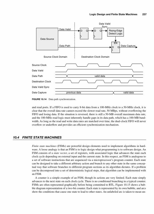
Logic Design and Finite State Machines 237
and read ports. If a FIFO is used to carry 8-bit data from a 100-MHz clock to a 50-MHz clock, it isclear that the overall data rate cannot exceed the slower read rate, 50 MBps, without overflowing theFIFO and losing data. If the situation is reversed, there is still a 50-MB overall maximum data rate,and the 100-MHz read logic must inherently handle gaps in its data path, which has a 100-MB band-width. As long as the read and write data rates are matched over time, the dual-clock FIFO will neveroverflow or underflow and provides an efficient synchronization mechanism.
10.4 FINITE STATE MACHINES
Finite state machines
(FSMs) are powerful design elements used to implement algorithms in hard-ware. A loose analogy is that an FSM is to logic design what programming is to software design. AnFSM consists of a
state vector
, a set of registers, with associated logic that advances the state eachclock cycle depending on external input and the current state. In this respect, an FSM is analogous toa set of software instructions that are sequenced via a microprocessor’s program counter. Each statecan be designed to take a different arbitrary action and branch to any other state in the same concep-tual way that software branches to different program sections as its algorithm dictates. If a problemcan be decomposed into a set of deterministic logical steps, that algorithm can be implemented withan FSM.
A counter is a simple example of an FSM, though its actions are very limited. Each state simplyadvances to the next state on each clock cycle. There is no conditional branching in a typical counter.FSMs are often represented graphically before being committed to RTL. Figure 10.15 shows a bub-ble diagram representation of a two-bit counter. Each state is represented by its own bubble, and arcsshow the conditions that cause one state to lead to other states. An unlabeled arc is taken to mean un-
Source Clock
Data Valid
Data Path
Destination Clock
Data Valid Sync
Data Capture
valid data
valid dataprevious data
D Q
Data Source
Data Valid
Data Path
D Q
D Q
EN
Data ValidSync
Source Clock Domain Destination Clock Domain
Data Capture
Rising-EdgeDetect Logic
FIGURE 10.14 Data path synchronization.
-Balch.book Page 237 Thursday, May 15, 2003 3:46 PM

238 Advanced Digital Systems
conditional or the default if no other conditional arcs are valid. Because this is a simple counter, eachstate has one unconditional arc that leads to the next state.
To illustrate basic FSM concepts, consider a stream of bytes being driven onto a data interfaceand a task to detect a certain pattern of data within that stream when a trigger signal is asserted. Thatpattern is the consecutive set of data 0x01, 0x02, 0x03, and 0x04. When this consecutive pattern hasbeen detected, an output detection flag should be set to indicate a match. The logic should never missdetecting this pattern, no matter what data precedes or follows it. After some consideration, the bub-ble diagram in Fig. 10.16 can be developed. It is common to name states with useful names such as“Idle” rather than binary numbers for readability. FSMs often sit in an idle or quiescent state whilethey wait for a triggering event that starts their execution.
The FSM waits in the Idle state until trigger is asserted. If the data value at this point is already0x01, the FSM skips directly to the Wait02 state. Otherwise, it branches to Wait01, where it remainsindefinitely until the value 0x01 is observed and it branches to Wait02. There are three possible arcscoming from Wait02. If the value 0x02 is observed, the FSM can advance to the third matching state,Wait03. If 0x01 is observed again, the FSM remains in Wait02, because 0x02 is the next value in thesequence following 0x01. If neither of these values is observed, the FSM branches back to Wait01 tostart over again. Wait03 is similar, although there is no arc to remain in the same state. If the first se-quence value, 0x01, is observed, the next state is Wait02. If Wait03 does succeed in immediately ob-serving 0x03, the FSM can advance to the final matching state, Wait04. If Wait04 immediatelyobserves 0x04, a match is declared by asserting the Match output flag, and the FSM completes itsfunction by returning to Idle. Otherwise, like in Wait03, the FSM branches back to Wait01 or Wait02.
"00"
"01"
"10"
"11"
FIGURE 10.15 Two-bit counter bubble diagram.
Idle Wait01
Wait02Wait03
trigger && data != 0x01
trigger && data == 0x01
!trigger data != 0x01
data == 0x01
data != 0x02&&
data != 0x01
data == 0x02
data == 0x04 /Match=1
data == 0x01
data != 0x03 &&data != 0x01
data == 0x01Wait04data == 0x03
data == 0x01
data != 0x04 &&data != 0x01
FIGURE 10.16 Pattern-matching FSM bubble diagram.
-Balch.book Page 238 Thursday, May 15, 2003 3:46 PM

Logic Design and Finite State Machines 239
FSMs are formally classified into one of two types:
Moore
and
Mealy
. A Moore FSM is onewherein the output signals are functions of only the current state vector. A Mealy FSM is one inwhich the output signals are functions of both the current state as well as the inputs to the FSM. Thepattern-matching FSM is a Mealy FSM, because Match is asserted when in state Wait04 and the in-put data is equal to 0x04. It could be converted into a Moore FSM by adding an additional state, per-haps called Matched, that would be inserted in the arc between Wait04 and Idle. The benefit of doingthis would be to reduce logic complexity, because the output signals are functions of only the statevector rather than the inputs as well. However, this comes at the cost of adding an extra state. AsFSMs get fairly complex, it may be too cumbersome to rigidly conform to a Moore design.
An FSM is typically coded in HDL using two blocks: a sequential (clocked) state vector blockand a combinatorial state and output assignment block. The pattern-matching FSM can be written inVerilog as shown in Fig. 10.17. Rather than calling out numerical state values directly in the RTL,constants are defined to make the code more readable. Verilog supports the
`define
construct that as-sociates a literal text string with a text identifier. The output, Match, is explicitly registered beforeleaving the module so that downstream logic timing will not be slowed down by incurring the pen-alty of the FSM logic. Registering the signal means that the output is that of a flop directly, ratherthan through an arbitrary number of logic gates that create additional timing delays.
In reading the FSM code, it can be seen that the state vector is three bits wide, because there arefive states in total. However, 2
3
equals 8, indicating that three of the possible state vector values areinvalid. Although none of these invalid values should ever arise, system reliability is increased by in-serting the
default
clause into the case statement. This assignment ensures that any invalid state willresult in the FSM returning to Idle. Without a default clause, any invalid state would not cause anyaction to be taken, and the FSM would remain in the same state indefinitely. It is good practice to in-sert default clauses into case statements when writing FSMs to guard against a hung condition. It isadmittedly unlikely that the state vector will assume an invalid value, but if a momentary glitch wereto happen, the design would benefit from a small amount of logic to restore the FSM to a valid state.
10.5 FSM BUS CONTROL
FSMs are well suited to managing arbitrarily complex bus interfaces. Microprocessors, memory de-vices, and I/O controllers can have interfaces with multiple states to handle arbitration between mul-tiple requestors, wait states, and multiword transfers (e.g., a burst SDRAM). Each of these bus statescan be represented by an FSM state, thereby breaking a seemingly complex problem into quite man-ageable pieces.
A simple example of CPU bus control is an asynchronous CPU interface with request/acknowl-edge signaling in which the FSM runs on a different clock from that of the CPU itself. AsynchronousCPU buses tend to implement four-corner handshaking to prevent the CPU and peripheral logicfrom getting out of step with one another. Two asynchronous control signals, chip select (CS_) andacknowledge (ACK_), can be managed with an FSM by breaking the distinct phases of a CPU ac-cess into separate states as shown in Fig. 10.18. The FSM waits in Idle until a synchronized CS_ isobserved, at which point it executes the transaction, asserts ACK_, and then transitions to the Ackstate. Once in Ack, the FSM waits until CS_ is deasserted before deasserting ACK_.
The logic is shown implemented in Verilog in Fig. 10.19. This FSM logic is simplistic in that itassumes that all transactions can be executed and acknowledged immediately. In reality, certain ap-plications will make such rapid execution impossible. A memory controller will need to insert la-tency while data is fetched, for example. Such situations can be handled by adding states to the FSMthat handle such cases. Rather than
Idle
immediately returning an acknowledge, it could initiate a
-Balch.book Page 239 Thursday, May 15, 2003 3:46 PM

240 Advanced Digital Systems
module PatternMatch ( Clk, Reset_, Trigger, Data, Match ); input Clk, Reset_, Trigger; input [7:0] Data; output Match; reg Match, NextMatch; reg [2:0] State, NextState; `define IDLE 3´h0 `define WAIT01 3´h1 `define WAIT02 3´h2 `define WAIT03 3´h3 `define WAIT04 3´h4 // sequential state vector block always @(posedge Clk) begin if (!Reset_) State[2:0] <= `IDLE; else State[2:0] <= NextState[2:0]; end // register output of FSM // could be combined with above state vector block if desired always @(posedge Clk) begin if (!Reset_) Match <= 1´b0; else Match <= NextMatch; end // FSM combinatorial logic always @(State[2:0] or Trigger or Data[7:0]) begin NextState[2:0] = State[2:0]; // default values prevent latches NextMatch = 1´b0; case (State[2:0]) `IDLE : if (Trigger && (Data[7:0] == 8´h01)) NextState[2:0] = `WAIT02; else if (Trigger) // data != 0x01 NextState[2:0] = `WAIT01;
FIGURE 10.17 Pattern-matching FSM logic.
-Balch.book Page 240 Thursday, May 15, 2003 3:46 PM

Logic Design and Finite State Machines 241
secondary transaction on behalf of the microprocessor and then transition to a state that waits untilthe secondary transaction completes before acknowledging the microprocessor.
It may appear that writing a formal FSM when the state vector is a single flop is too cumbersome.Equivalent functionality can be obtained with a simple if…else structure instead of a case statementand separate vector assignment block. The advantages to coding the FSM in a formal manner areconsistency and ease of maintenance. If the logic grows in complexity to include more states, it willbe relatively easy to augment an existing FSM structure rather than rewriting one from an if…else
`WAIT01 : if (Data[7:0] == 8´h01) NextState[2:0] = `WAIT02; // else not required due to default assignment above
`WAIT02 : if (Data[7:0] == 8´h01) NextState[2:0] = `WAIT02; else if (Data[7:0] == 8´h02) NextState[2:0] = `WAIT03; else // data != 0x01 or 0x02 NextState[2:0] = `WAIT01;
`WAIT03 : if (Data[7:0] == 8´h01) NextState[2:0] = `WAIT02; else if (Data[7:0] == 8´h03) NextState[2:0] = `WAIT04; else // data != 0x01 or 0x03 NextState[2:0] = `WAIT01; `WAIT04 : if (Data[7:0] == 8´h01) NextState[2:0] = `WAIT02; else if (Data[7:0] == 8´h04) begin NextState[2:0] = `IDLE; NextMatch = 1´b1; end else // data != 0x01 or 0x04 NextState[2:0] = `WAIT01; default : NextState[2:0] = `IDLE; // handle unknown state vectors endcase end endmodule
FIGURE 10.17 (continued) Pattern-matching FSM logic.
Idle Ack
!CS_ /ClrAck=1, Do read/write
CS_ !CS_
CS_ /SetAck=1
FIGURE 10.18 Asynchronous bus slave FSM bubble diagram.
-Balch.book Page 241 Thursday, May 15, 2003 3:46 PM

242 Advanced Digital Systems
reg State, NextState; reg CS_Input_, CS_Sync_, CpuAck_; `define IDLE 1´h0 `define ACK 1´h1 always @(posedge Clk) begin if (!Reset_) State <= `IDLE; else State <= NextState; end // FSM support logic: synchronization and registered output always @(posedge Clk) begin if (!Reset_) begin CS_Input_ <= 1´b1; // active low signals reset to high CS_Sync_ <= 1´b1; CpuAck_ <= 1´b1; end else begin CS_Input_ <= CS_; // first synchronizer stage CS_Sync_ <= CS_Input_; // second synchronizer stage if (SetAck) CpuAck_ <= 1´b1;
else if (ClrAck) CpuAck_ <= 1´b0; end
end
// FSM logic assumes supporting logic: // // CpuDataOE enables tristate output for reads // WriteEnable enables writes to registers decoded from address inputs
always @(State or CS_Sync_ or Rd_ or Wr_) begin NextState = State; // default values prevent latches
ClrAck = 1´b0; CpuDataOE = 1´b0; SetAck = 1´b0; WriteEnable = 1´b0;
case (State)
`IDLE : if (!CS_Sync_) begin NextState = `ACK; ClrAck = 1´b1; CpuDataOE = !Rd_; WriteEnable = !Wr_; end
`ACK : if (CS_Sync_) begin // wait for CS_ deassertion NextState = `IDLE; SetAck = 1´b1; end
endcase end
FIGURE 10.19 Asynchronous bus slave logic.
-Balch.book Page 242 Thursday, May 15, 2003 3:46 PM
Logic Design and Finite State Machines 243
construct. Real bus control FSMs typically requires additional states to handle more complex trans-action. In the end, the decision is a matter of individual preference and style.
10.6 FSM OPTIMIZATION
FSM complexity can rapidly get out of hand when designing logic to execute a complex algorithm.Two related ways in which complexity manifests itself are excessively large FSMs and timing prob-lems. FSMs with dozens of states can, on their own, lead to timing problems resulting from themany levels of logic necessary to map the full set of inputs and the current state vector to the full setof outputs and the next state vector. Yet, even FSMs with relatively few states can exhibit timingproblems if the branch conditions get overly complex.
When complex branch conditions are combined with a very large FSM, the result can be a timingnightmare if suitable design decisions are not made from the beginning. A conceivably poor resultcould be logic that needs to run at 66 MHz being barely capable of 20-MHz operation. In most in-stances, an acceptable level of performance can be obtained by properly optimizing the FSM and itssupporting logic from the start. If this is not true, chances are that a fundamental change is necessaryin either the implementation technology (e.g., faster logic circuits) or the overall architectural ap-proach to solving the problem (e.g., more parallelism in dividing a task into smaller pieces). FSMtiming optimization techniques include partitioning, state vector encoding methods, and pipelining.
Proper partitioning of FSMs, and logic in general, is a major factor in successful systems develop-ment. Even the best optimization schemes can fail if the underlying FSM is improperly structured. Itis usually better to design a system with multiple smaller FSMs instead of a few large ones. Smallerlogic structures will tend to have fewer inputs, thereby reducing the complexity of the logic and im-proving its performance. When the interfaces between multiple FSMs are registered, long timingpaths are broken to isolate each FSM from a timing perspective. Without registered interfaces, it ispossible for multiple FSMs to form a large loop of dense logic as one feeds back to another. Thiswould defeat a primary benefit of designing smaller FSMs.
Partitioning functionality across smaller FSMs not only makes it easier to improve their timing, italso makes it easier to design and debug the logic. Each smaller section of logic can be assigned to adifferent engineer for concurrent development, or the sections can be developed serially in a progres-sive manner by designing and testing each element sequentially. By the time the entire design hasbeen completed, the daunting task of simulating everything at once can be substantially minimized,because each section has already been tested individually. Bugs are likely to arise when all thepieces are put together, but the overall magnitude of the debugging process should be reduced.
State-vector encoding methods are most often considered as a choice between two options:
binaryencoding
and
one-hot encoding
. A binary encoded FSM is equivalent to the examples presented ear-lier in this chapter: a state vector is chosen with N flops such that 2
N
is greater than or equal to thetotal number of states in the FSM. Each state is assigned a unique value in the range of 0 to 2
N
– 1. Aone-hot FSM allocates one state flop for each unique state and adheres to a rule that only one flop isset (hot) on any single cycle. The benefits of a one-hot FSM include reduced complexity of outputlogic and reduced power consumption. Output logic complexity is often reduced by one-hot encod-ing, because the entire state vector does not have to be decoded. Instead, only those state flops thatdirectly map to an output signal are included in the Boolean expression. Power consumption is re-duced, because only two flops change state at a time (the old state flop transitions from high to low,and the new state flop transitions from low to high) instead of many or all state bits. The decision toimplement one-hot encoding varies according to the size of the FSM and the constraints of the im-plementation technology. Beyond a certain size, one-hot encoding becomes too unwieldy and mayactually result in more logic than a binary encoded version. Different technologies (e.g., custom ver-
-Balch.book Page 243 Thursday, May 15, 2003 3:46 PM
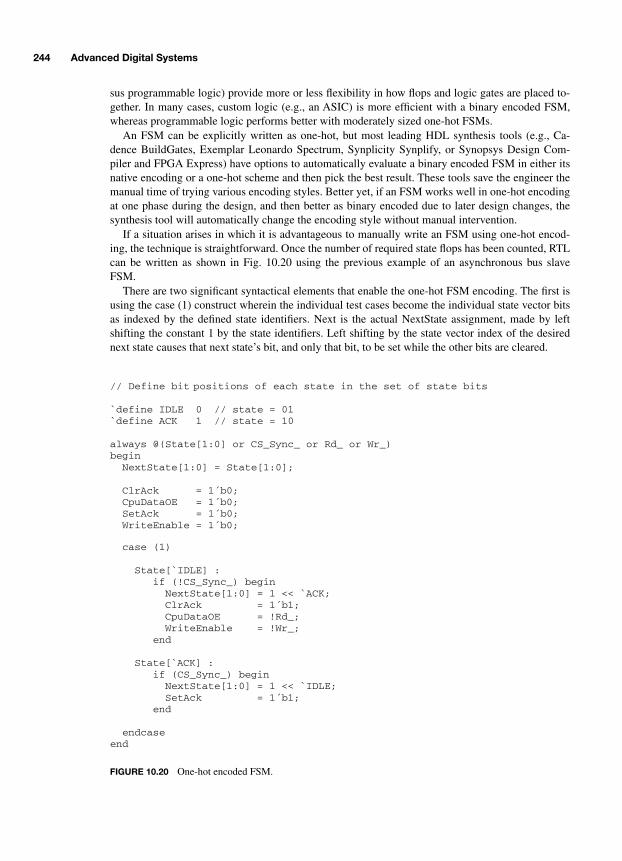
244 Advanced Digital Systems
sus programmable logic) provide more or less flexibility in how flops and logic gates are placed to-gether. In many cases, custom logic (e.g., an ASIC) is more efficient with a binary encoded FSM,whereas programmable logic performs better with moderately sized one-hot FSMs.
An FSM can be explicitly written as one-hot, but most leading HDL synthesis tools (e.g., Ca-dence BuildGates, Exemplar Leonardo Spectrum, Synplicity Synplify, or Synopsys Design Com-piler and FPGA Express) have options to automatically evaluate a binary encoded FSM in either itsnative encoding or a one-hot scheme and then pick the best result. These tools save the engineer themanual time of trying various encoding styles. Better yet, if an FSM works well in one-hot encodingat one phase during the design, and then better as binary encoded due to later design changes, thesynthesis tool will automatically change the encoding style without manual intervention.
If a situation arises in which it is advantageous to manually write an FSM using one-hot encod-ing, the technique is straightforward. Once the number of required state flops has been counted, RTLcan be written as shown in Fig. 10.20 using the previous example of an asynchronous bus slaveFSM.
There are two significant syntactical elements that enable the one-hot FSM encoding. The first isusing the case (1) construct wherein the individual test cases become the individual state vector bitsas indexed by the defined state identifiers. Next is the actual NextState assignment, made by leftshifting the constant 1 by the state identifiers. Left shifting by the state vector index of the desirednext state causes that next state’s bit, and only that bit, to be set while the other bits are cleared.
// Define bit positions of each state in the set of state bits `define IDLE 0 // state = 01 `define ACK 1 // state = 10 always @(State[1:0] or CS_Sync_ or Rd_ or Wr_) begin NextState[1:0] = State[1:0]; ClrAck = 1´b0; CpuDataOE = 1´b0; SetAck = 1´b0; WriteEnable = 1´b0; case (1) State[`IDLE] : if (!CS_Sync_) begin NextState[1:0] = 1 << `ACK; ClrAck = 1´b1; CpuDataOE = !Rd_; WriteEnable = !Wr_; end State[`ACK] : if (CS_Sync_) begin NextState[1:0] = 1 << `IDLE; SetAck = 1´b1; end endcase end
FIGURE 10.20 One-hot encoded FSM.
-Balch.book Page 244 Thursday, May 15, 2003 3:46 PM

Logic Design and Finite State Machines 245
10.7 PIPELINING
Pipelining is a significant method of improving FSM timing in a way similar to normal logic. Acomplex FSM contains a large set of inputs that feeds the next state logic. As the number of branchvariables across the entire FSM increases, long timing paths quickly develop. It is advantageous toprecompute many branch conditions and reduce a condition to a binary variable: true or false. In do-ing so, the branch variables are moved away from the FSM logic and behind a pipeline flop. Thelogic delay penalty of evaluating the branch condition is hidden by the pipeline flop. This simplifiesthe FSM logic because it has to evaluate only the true/false condition result, which is a function ofone variable, instead of the whole branch condition, which can be a function of many variables.
An example of using pipelining to improve FSM timing is whereby an FSM is counting eventsand waits in a particular state until the event has occurred N times, at which point the FSM branchesto a new state. In this situation, a counter lies off to the side of the FSM, and the FSM asserts a signalto increment the counter each time a particular event occurs. Without pipelining, the FSM wouldcompare the counter bits against the constant, N, as a branch condition. If the counter is eight bitswide, there is a function of eight variables plus any other qualifiers. If the counter is 16 bits wide, atleast 16 variables are present. Many such Boolean equations in the same FSM can lead to timingproblems.
Pipelining can be implemented by performing the comparison outside of the FSM with the true/false result being stored in a flop that is directly evaluated by the FSM, thereby reducing the evalua-tion to a function of only one variable. The trick to making this work properly is that the latency ofthe pipelined comparison needs to be built into both the comparison logic and the FSM itself.
In a counter situation without pipelining, the FSM increments the counter when an event occursand simultaneously evaluates the current count value to determine if N events have occurred. There-fore, the FSM would have to make its comparison against N – 1 instead of against N if it wanted toreact at the proper time. When the counter is at N – 1 and the event occurs, the FSM knows that thisevent is the Nth event in the sequence.
Inserting a pipeline flop into the counter comparison logic adds a cycle of latency to the compari-son. The FSM cannot simply look ahead an additional cycle to N – 2, because it cannot tell the fu-ture: it does not ordinarily know if an event will occur in the next cycle. This problem can beaddressed in the pipelined comparison logic. The comparison logic must be triggered at N – 2 so thatthe FSM can observe the asserted signal on the following cycle when the counter is at N – 1, whichenables the FSM to operate as before to recognize the Nth event. Because an ultimate comparison toN – 1 is desired, the pipelined logic can evaluate the expression, “If count equals N – 2 and incre-ment is true, then count will equal N – 1 in the next cycle.” In the next cycle, the FSM will have theknowledge that count equals N – 1 from a single flop, and it can qualify this in the same way it didwithout the pipelining with the end same result. Verilog code fragments to implement this schemeare shown in Fig. 10.21, where the FSM completes its task when 100 events have been observed.
Pipelining should be carefully considered when an FSM is evaluating long bit vectors if it is be-lieved that proper timing will be difficult to achieve. Counter comparisons to constants are not theonly candidates for pipelining. Valid pipelining candidates include counter comparisons to other reg-isters and arithmetic embedded within branch conditions. Arithmetic expressions such as one shownin Fig. 10.22 can add long timing paths to an already complex FSM.
Adding two vectors and then comparing their sum to a third vector is a substantial quantity oflogic. Such situations are not uncommon in an FSM that must negotiate complex algorithms. Itwould be highly advantageous to perform the arithmetic and comparison in a pipelined manner sothat the FSM would have to evaluate only a single flop. The complexity involved in pipelining suchan expression is highly dependent on the application’s characteristics. Pipelining can get tricky whenit becomes necessary to look ahead one cycle and deal with possible exceptions to the look-ahead
-Balch.book Page 245 Thursday, May 15, 2003 3:46 PM

246 Advanced Digital Systems
process. Despite this complexity, there are situations in which this is the only way of obtaining thedesired performance.
Pipelining is perhaps most tricky when the logic involved contains a feedback path through theFSM. This feedback path can be of the type discussed previously whereby the FSM is detecting anevent, incrementing a counter, and then relying on that count value to take further action. There areother situations in which no feedback path exists. An FSM may be called on to process an incomingdata stream over which it has no direct control. As in the earlier pattern matching example, the FSMmay need to look for certain data values and take action if they are located. In Fig. 10.17, the FSMdirectly evaluated the eight-bit data stream in searching for the values 0x01, 0x02, 0x03, and 0x04.This logic can be optimized by inserting pattern-matching flops between the data input port and theFSM as shown in Fig. 10.23. In doing so, the FSM no longer needs to evaluate the entire eight-bitvector but instead can test a single flop for each pattern.
`define COMPARE_VALUE 7´d98 // N - 2 due to pipeline delay
// counter logic with pipelined comparison logic
always @(posedge Clk) begin if (ClrCount) begin CountDone <= 1´b0; Count[6:0] <= 8´h1; end else if (IncCount) begin CountDone <= Count[6:0] == `COMPARE_VALUE; Count[6:0] <= Count[6:0] + 1; end
end
// Partial FSM logic
... `WAIT_COUNT : if (Event && CountDone) // N-1 CountDone flag qualified with NextState[3:0] = `FINISH; // Event, indicating Nth event else if (Event) IncCount = 1´b1; ... end
...
FIGURE 10.21 Pipelined count comparison logic.
`COMPLEX_STATE : if ( (BytesFound[15:0] + BytesOffset[7:0]) > BytesThreshold[15:0] ) NextState[3:0] = `MORE_MATH; ... else ... end ...
FIGURE 10.22 Arithmetic expression in FSM branch condition.
-Balch.book Page 246 Thursday, May 15, 2003 3:46 PM
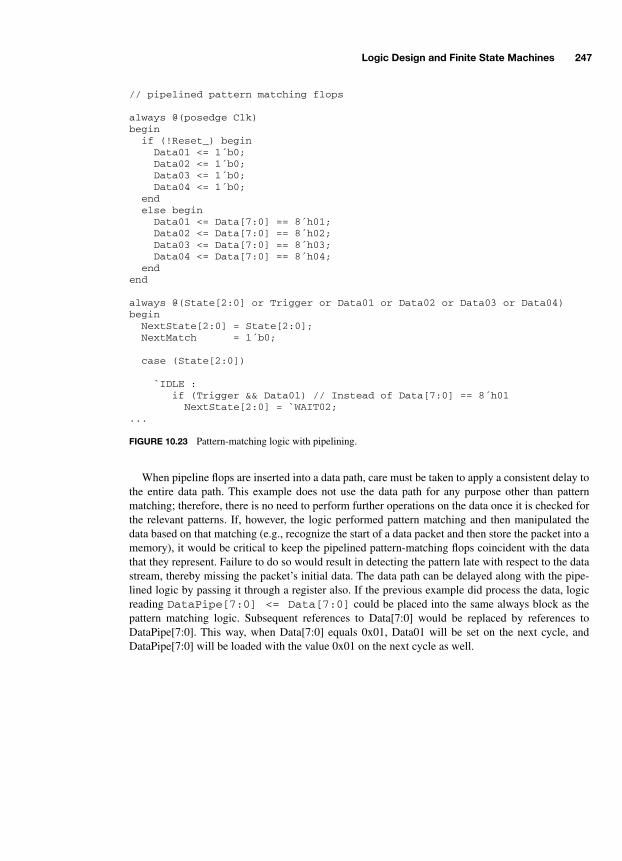
Logic Design and Finite State Machines 247
When pipeline flops are inserted into a data path, care must be taken to apply a consistent delay tothe entire data path. This example does not use the data path for any purpose other than patternmatching; therefore, there is no need to perform further operations on the data once it is checked forthe relevant patterns. If, however, the logic performed pattern matching and then manipulated thedata based on that matching (e.g., recognize the start of a data packet and then store the packet into amemory), it would be critical to keep the pipelined pattern-matching flops coincident with the datathat they represent. Failure to do so would result in detecting the pattern late with respect to the datastream, thereby missing the packet’s initial data. The data path can be delayed along with the pipe-lined logic by passing it through a register also. If the previous example did process the data, logicreading
DataPipe[7:0] <= Data[7:0]
could be placed into the same always block as thepattern matching logic. Subsequent references to Data[7:0] would be replaced by references toDataPipe[7:0]. This way, when Data[7:0] equals 0x01, Data01 will be set on the next cycle, andDataPipe[7:0] will be loaded with the value 0x01 on the next cycle as well.
// pipelined pattern matching flops
always @(posedge Clk) begin if (!Reset_) begin Data01 <= 1´b0; Data02 <= 1´b0; Data03 <= 1´b0; Data04 <= 1´b0; end else begin Data01 <= Data[7:0] == 8´h01; Data02 <= Data[7:0] == 8´h02; Data03 <= Data[7:0] == 8´h03; Data04 <= Data[7:0] == 8´h04; end
end
always @(State[2:0] or Trigger or Data01 or Data02 or Data03 or Data04) begin NextState[2:0] = State[2:0]; NextMatch = 1´b0;
case (State[2:0])
`IDLE : if (Trigger && Data01) // Instead of Data[7:0] == 8´h01 NextState[2:0] = `WAIT02;
...
FIGURE 10.23 Pattern-matching logic with pipelining.
-Balch.book Page 247 Thursday, May 15, 2003 3:46 PM

This page intentionally left blank.

249
CHAPTER 11
Programmable Logic Devices
Programmable logic is the means by which a large segment of engineers implement their customlogic, whether that logic is a simple I/O port or a complex state machine. Most programmable logicis implemented with some type of HDL that frees the engineer from having to derive and minimizeBoolean expressions each time a new logical relationship is designed. The advantages of program-mable logic include rapid customization with relatively limited expense invested in tools and sup-port.
The widespread availability of flexible programmable logic products has brought custom logicdesign capabilities to many individuals and smaller companies that would not otherwise have the fi-nancial and staffing resources to build a fully custom IC. These devices are available in a wide rangeof sizes, operating voltages, and speeds, which all but guarantees that a particular application can beclosely matched with a relevant device. Selecting that device requires some research, because eachmanufacturer has a slightly different specialty and range of products.
Programmable logic technology advances rapidly, and manufacturers are continually offering de-vices with increased capabilities and speeds. After completing this chapter and learning about thebasic types of devices that are available, it is recommended that you to browse through the latestmanufacturers’ data sheets to get updated information. Companies such as Altera, Atmel, Cypress,Lattice, QuickLogic, and Xilinx provide detailed data sheets on their web sites and also tend to offerbundled development software for reasonable prices.
11.1 CUSTOM AND PROGRAMMABLE LOGIC
Beyond using discrete 7400 ICs, custom logic is implemented in larger ICs that are either manufac-tured with custom masks at a factory or programmed with custom data images at varying points afterfabrication. Custom ICs, or
application specific integrated circuits
(ASICs), are the most flexible op-tion because, as with anything custom, there are fewer constraints on how application specific logicis implemented. Because custom ICs are tailored for a specific application, the potential exists forhigh clock speeds and relatively low unit prices. The disadvantages to custom ICs are long and ex-pensive development cycles and the inability to make quick logic changes. Custom IC developmentcycles are long, because a design must generally be frozen in a final state before much of the siliconlayout and circuit design work can be completed. Engineering charges for designing a custom maskset (not including the logic design work) can range from $50,000 to well over $1 million, dependingon the complexity. Once manufactured, the logic can’t simply be altered, because the logic configu-ration is an inherent property of the custom design. If a bug is found, the time and money to alter themask set can approach that of the initial design itself.
-Balch.book Page 249 Thursday, May 15, 2003 3:46 PM
Copyright 2003 by The McGraw-Hill Companies, Inc. Click Here for Terms of Use.
250 Advanced Digital Systems
Programmable logic devices
(PLDs) are an alternative to custom ASICs. A PLD consists of gen-eral-purpose logic resources that can be connected in many permutations according to an engineer’slogic design. This programmable connectivity comes at the price of additional, hidden logic thatmakes logic connections within the chip. The main benefit of PLD technology is that a design can berapidly loaded into a PLD, bypassing the time consuming and expensive custom IC developmentprocess. It follows that if a bug is found, a fix can be implemented very quickly and, in many cases,reprogrammed into the existing PLD chip. Some PLDs are one-time programmable, and some canbe reprogrammed in circuit.
The disadvantage of PLDs is the penalty paid for the hidden logic that implements the program-mable connectivity between logic gates. This penalty manifests itself in three ways: higher unit cost,slower speeds, and increased power consumption. Programmable gates cost more than custom gates,because, when a programmable gate is purchased, that gate plus additional connectivity overhead isactually being paid for. Propagation delay is an inherent attribute of all silicon structures, and themore structures that are present in a path, the slower the path will be. It follows that a programmablegate will be slower than a custom gate, because that programmable gate comes along with additionalconnectivity structures with their own timing penalties. The same argument holds true for powerconsumption.
Despite the downside of programmable logic, the technology as a whole has progressed dramati-cally and is extremely popular as a result of competitive pricing, high performance levels, and, espe-cially, quick time to market. Time to market is an attribute that is difficult to quantify but one that isalmost universally appreciated as critical to success. PLDs enable a shorter development cycle, be-cause designs can be prototyped rapidly, the bugs worked out, and product shipped to a customer be-fore some ASIC technologies would even be in fabrication. Better yet, if a bug is found in the field,it may be fixable with significantly less cost and disruption. In the early days of programmable logic,PLDs could not be reprogrammed, meaning that a bug could still force the recall of product alreadyshipped. Many modern reprogrammable PLDs allow hardware bugs to be fixed in the field with asoftware upgrade consisting of a new image that can be downloaded to the PLD without having toremove the product from the customer site.
Cost and performance are probably the most debated trade-offs involved in using programmablelogic. The full range of applications in which PLDs or ASICs are considered can be broadly splitinto three categories as shown in Fig. 11.1. At the high end of technology, there are applications inwhich an ASIC is the only possible solution because of leading edge timing and logic density re-quirements. In the mid range, clock frequencies and logic complexity are such that a PLD is capableof solving the problem, but at a higher unit cost than an ASIC. Here, the decision must be made be-tween flexibility and time to market versus lowest unit cost. At the low end, clock frequencies andlogic density requirements are far enough below the current state of silicon technology that a PLDmay meet or even beat the cost of an ASIC.
It may sound strange that a PLD with its overhead can ever be less expensive than a custom chip.The reasons for this are a combination of silicon die size and volume pricing. Two of the major fac-tors in the cost of fabricating a working silicon die are its size and manufacturing yield. As a die getssmaller, more of them can be fabricated at the same time on the same wafer using the same re-sources. IC manufacturing processes are subject to a certain yield, which is the percentage of work-ing dice obtained from an overall lot of dice. Some dice develop microscopic flaws duringmanufacture that make them unusable. Yield is a function of many variables, including the reliabilityof uniformly manufacturing a certain degree of complexity given the prevailing state of technologyat a point in time. From these two points, it follows that a silicon chip will be less expensive to man-ufacture if it is both small and uses a technology process that is mature and has a high yield.
At the low end of speed and density, a small PLD and a small ASIC may share the same maturetechnology process and the same yield characteristics, removing yield as a significant variable in
-Balch.book Page 250 Thursday, May 15, 2003 3:46 PM
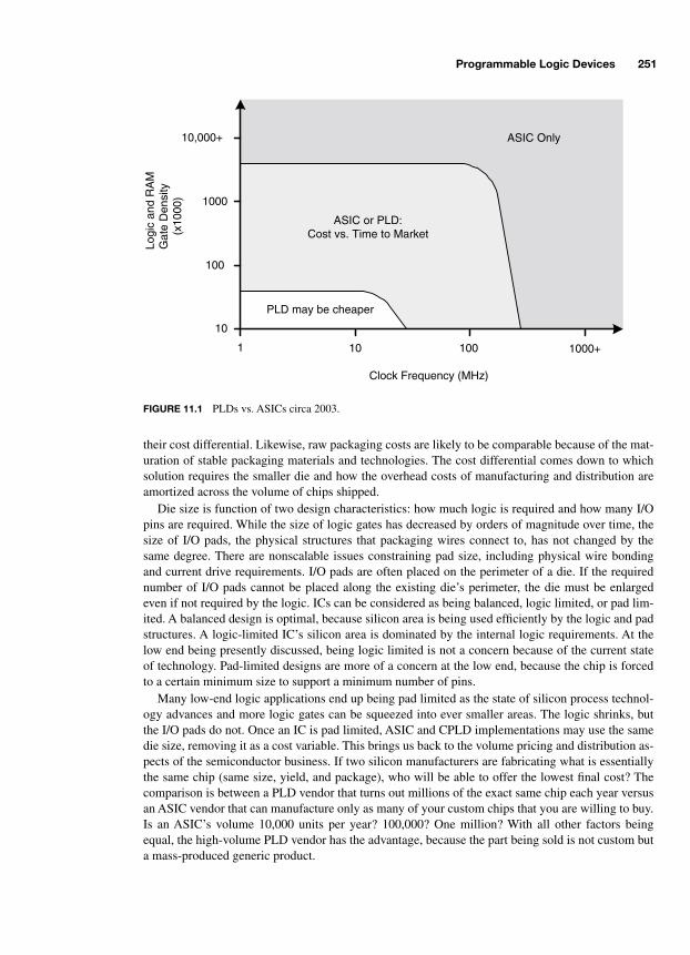
Programmable Logic Devices 251
their cost differential. Likewise, raw packaging costs are likely to be comparable because of the mat-uration of stable packaging materials and technologies. The cost differential comes down to whichsolution requires the smaller die and how the overhead costs of manufacturing and distribution areamortized across the volume of chips shipped.
Die size is function of two design characteristics: how much logic is required and how many I/Opins are required. While the size of logic gates has decreased by orders of magnitude over time, thesize of I/O pads, the physical structures that packaging wires connect to, has not changed by thesame degree. There are nonscalable issues constraining pad size, including physical wire bondingand current drive requirements. I/O pads are often placed on the perimeter of a die. If the requirednumber of I/O pads cannot be placed along the existing die’s perimeter, the die must be enlargedeven if not required by the logic. ICs can be considered as being balanced, logic limited, or pad lim-ited. A balanced design is optimal, because silicon area is being used efficiently by the logic and padstructures. A logic-limited IC’s silicon area is dominated by the internal logic requirements. At thelow end being presently discussed, being logic limited is not a concern because of the current stateof technology. Pad-limited designs are more of a concern at the low end, because the chip is forcedto a certain minimum size to support a minimum number of pins.
Many low-end logic applications end up being pad limited as the state of silicon process technol-ogy advances and more logic gates can be squeezed into ever smaller areas. The logic shrinks, butthe I/O pads do not. Once an IC is pad limited, ASIC and CPLD implementations may use the samedie size, removing it as a cost variable. This brings us back to the volume pricing and distribution as-pects of the semiconductor business. If two silicon manufacturers are fabricating what is essentiallythe same chip (same size, yield, and package), who will be able to offer the lowest final cost? Thecomparison is between a PLD vendor that turns out millions of the exact same chip each year versusan ASIC vendor that can manufacture only as many of your custom chips that you are willing to buy.Is an ASIC’s volume 10,000 units per year? 100,000? One million? With all other factors beingequal, the high-volume PLD vendor has the advantage, because the part being sold is not custom buta mass-produced generic product.
Logi
c an
d R
AM
Gat
e D
ensi
ty(x
1000
)
Clock Frequency (MHz)
10 1001 1000+
10
100
1000
10,000+ ASIC Only
ASIC or PLD:Cost vs. Time to Market
PLD may be cheaper
FIGURE 11.1 PLDs vs. ASICs circa 2003.
-Balch.book Page 251 Thursday, May 15, 2003 3:46 PM

252 Advanced Digital Systems
11.2 GALS AND PALS
Among the most basic types of PLDs are Generic Array Logic
TM
(GAL) devices.
*
GALs are en-hanced variants of the older Programmable Array Logic
TM
(PAL) architecture that is now essentiallyobsolete. The term PAL is still widely used, but people are usually referring to GAL devices or otherPLD variants when they use the term. PALs became obsolete, because GALs provide a superset oftheir functionality and can therefore perform all of the functions that PALs did. GALs are relativelysmall, inexpensive, easily available, and manufactured by a variety of vendors (e.g., Cypress, Lat-tice, and Texas Instruments).
It can be shown through Boolean algebra that any logical expression can be represented as an ar-bitrarily complex sum of products. Therefore, by providing a programmable array of AND/ORgates, logic can be customized to fit a particular application. GAL devices provide an extensive pro-grammable array of wide AND gates, as shown in Fig. 11.2, into which all the device’s input termsare fed. Both true and inverted versions of each input are made available to each AND gate. The out-puts of groups of AND gates (products) feed into separate OR gates (sums) to generate user-definedBoolean expressions.
Each intersection of a horizontal AND gate line and a vertical input term is a programmable con-nection. In the early days of PLDs, these connections were made by fuses that would literally have tobe blown with a high voltage to configure the device. Fuse-based devices were not reprogrammable;
* GAL, Generic Array Logic, PAL, and Programmable Array Logic are trademarks of Lattice Semiconductor Corporation.
Input Terms
AND/OROutput Terms
FIGURE 11.2 GAL/PAL AND/OR structure.
-Balch.book Page 252 Thursday, May 15, 2003 3:46 PM

Programmable Logic Devices 253
once a microscopic fuse is blown, it cannot be restored. Today’s devices typically rely on EEPROMtechnology and CMOS switches to enable nonvolatile reprogrammability. However, fuse-based ter-minology remains in use for historical reasons. The default configuration of a connection emulatesan intact fuse, thereby connecting the input term to the AND gate input. When the connection isblown, or programmed, the AND input is disconnected from the input term and pulled high to effec-tively remove that input from the Boolean expression. Customization of a GAL’s programmableAND gate is conceptually illustrated in Fig. 11.3.
With full programmability of the AND array, the OR connections can be hard wired. Each GALdevice feeds a differing number of AND terms into the OR gates. If one or more of these AND termsare not needed by a particular Boolean expression, those unneeded AND gates can be effectively dis-abled by forcing their outputs to 0. This is done by leaving an unneeded AND gate’s inputs unpro-grammed. Remember that inputs to the AND array are provided in both true and complementversions. When all AND connections are left intact, multiple expressions of the form re-sult, thereby forcing that gate’s output to 0 and rendering it nonparticipatory in the OR function.
The majority of a GAL’s logic customization is performed by programming the AND array. How-ever, selecting flip-flops, OR/NOR polarities, and input/output configurations is performed by pro-gramming a configurable I/O and feedback structure called a
macrocell
. The basic concept behind amacrocell is to ultimately determine how the AND/OR Boolean expression is handled and how themacrocell’s associated I/O pin operates. A schematic view of a GAL macrocell is shown in Fig. 11.4,although some GALs may contain macrocells with slightly different capabilities. Multiplexers deter-mine the polarity of the final OR/NOR term, regardless of whether the term is registered andwhether the feedback signal is taken directly at the flop’s output or at the pin. Configuring the mac-rocell’s output enable determines how the pin behaves.
A B C D E F
A B C D E FA B C D E F
Programmed Connection
Output = A & C & D & E & F
FIGURE 11.3 Programming AND input terms.
A&A 0=
AND ArrayTerms
ConfigurationInformation
OutputEnable
Feedback toAND Array
D Q
Clock
ConfigurationInformation
I/OPin
FIGURE 11.4 GAL macrocell.
-Balch.book Page 253 Thursday, May 15, 2003 3:46 PM
254 Advanced Digital Systems
There are two common GAL devices, the 16V8 and the 22V10, although other variants exist aswell. They contain eight and ten macrocells each, respectively. The 16V8 provides up to 10 dedi-cated inputs that feed the AND array, whereas the 22V10 provides 12 dedicated inputs. One of the22V10’s dedicated inputs also serves as a global clock for any flops that are enabled in the macro-cells. Output enable logic in a 22V10 is evaluated independently for each macrocell via a dedicatedAND term. The 16V8 is somewhat less flexible, because it cannot arbitrarily feed back all macrocelloutputs depending on the device configuration. Additionally, when configured for registered modewhere macrocell flops are usable, two dedicated input pins are lost to clock and output enable func-tions.
GALs are fairly low-density PLDs by modern standards, but their advantages of low cost andhigh speed are derived from their small size. Implementing logic in a GAL follows several basicsteps. First, the logic is represented in either graphical schematic diagram or textual (HDL) form.This representation is converted into a netlist using a translation or synthesis tool. Finally, thenetlist is fitted into the target device by mapping individual gate functions into the programmableAND array. Given the fixed AND/OR structure of a GAL, fitting software is designed to performlogic optimizations and translations to convert arbitrary Boolean expressions into sum-of-productexpressions. The result of the fitting process is a programming image, also called a
fuse map
, thatdefines exactly which connections, or fuses, are to be programmed and which are to be left at theirdefault state. The programming image also contains other information such as macrocell configura-tion and other device-specific attributes.
Modern PLD development software allows the back-end GAL synthesis and fitting process toproceed without manual intervention in most cases. The straightforward logic flow through the pro-grammable AND array reduces the permutations of how a given Boolean expression can be imple-mented and results in very predictable logic fitting. An input signal propagates through the pin andpad structure directly into the AND array, passes through just two gates, and can then either feed amacrocell flop or drive directly out through an I/O pin. Logic elements within a GAL are close toeach other as a result of the GAL’s small size, which contributes to low internal propagation delays.These characteristics enable the GAL architecture to deliver very fast timing specifications, becausesignals follow deterministic paths with low propagation delays.
GALs are a logic implementation technology with very predictable capabilities. If the desiredlogic cannot fit within the GAL, there may not be much that can be done without optimizing the al-gorithm or partitioning the design across multiple devices. If the logic fits but does not meet timing,the logic must be optimized, or a faster device must be found. Because of the GAL’s basic fittingprocess and architecture, there isn’t the same opportunity of tweaking the device as can be done withmore complex PLDs. This should not be construed as a lack of flexibility on the part of the GAL.Rather, the GAL does what it says it does, and it is up to the engineer to properly apply the technol-ogy to solve the problem at hand. It is the simplicity of the GAL architecture that is its greateststrength.
Lattice Semiconductor’s GAL22LV10D-4 device features a worst-case input-to-output combina-torial propagation delay of just 4 ns.
*
This timing makes the part suitable for address decoding onfast microprocessor interfaces. The same 22V10 part features a 3-ns t
CO
and up to 250-MHz opera-tion. The t
CO
specification is a pin-to-pin metric that includes the propagation delays of the clockthrough the input pin and the output signal through the output pin. Internally, the actual flop itselfexhibits a faster t
CO
that becomes relevant for internal logic feedback paths. Maximum clock fre-quency specifications are an interesting aspect of all PLDs and some consideration. These specifica-tions are best-case numbers usually obtained with minimal logic configurations. They may define
* GAL22LV10D, 22LV10_04, Lattice Semiconductor, 2000, p. 7.
-Balch.book Page 254 Thursday, May 15, 2003 3:46 PM

Programmable Logic Devices 255
the highest toggle rate of the device’s flops, but synchronous timing analysis dictates that there ismore to f
MAX
than the flop’s t
SU
and t
CO
. Propagation delay of logic and connectivity between flopsis of prime concern. The GAL architecture’s deterministic and fast logic feedback paths reduces theadded penalty of internal propagation delays. Lattice’s GAL22LV10D features an internal clock-to-feedback delay of 2.5 ns, which is the combination of the actual flop’s t
CO
plus the propagation delayof the signal back through the AND/OR array. This feedback delay, when combined with the flop’s3-ns t
SU
, yields a practical f
MAX
of 182 MHz when dealing with most normal synchronous logic thatcontains feedback paths (e.g., a state machine).
11.3 CPLDS
Complex PLDs
, or CPLDs, are the mainstream macrocell-based PLDs in the industry today, provid-ing logic densities and capabilities well beyond those of a GAL device. GALs are flexible for theirsize because of the large programmable AND matrix that defines logical connections between inputsand outputs. However, this anything-to-anything matrix makes the architecture costly to scale tohigher logic densities. For each macrocell that is added, both matrix dimensions grow as well.Therefore, the AND matrix increases in a square function of the I/O terms and macrocells in the de-vice. CPLD vendors seek to provide a more linear scaling of connectivity resources to macrocells byimplementing a segmented architecture with multiple fixed-size GAL-style logic blocks that are in-terconnected via a central switch matrix as shown in Fig. 11.5. Like a GAL, CPLDs are typicallymanufactured with EEPROM configuration storage, making their function nonvolatile. After pro-gramming, a CPLD will retain its configuration and be ready for operation when power is applied tothe system.
Each individual logic block is similar to a GAL and contains its own programmable AND/OR ar-ray and macrocells. This approach is scalable, because the programmable AND/OR arrays remainfixed in size and small enough to fabricate economically. As more macrocells are integrated onto thesame chip, more logic blocks are placed onto the chip instead of increasing the size of individuallogic blocks and bloating the AND/OR arrays. CPLDs of this type are manufactured by companiesincluding Altera, Cypress, Lattice, and Xilinx.
Logic BlockInput Term
SwitchMatrix
I/O Cells
GAL-TypeLogic Block
Input Terms
FeedbackPin Outputs
Pin Inputs
GAL-TypeLogic Block
Input Terms
FeedbackPin Outputs
GAL-TypeLogic Block
Input Terms
FeedbackPin Outputs
FIGURE 11.5 Typical CPLD architecture.
-Balch.book Page 255 Thursday, May 15, 2003 3:46 PM
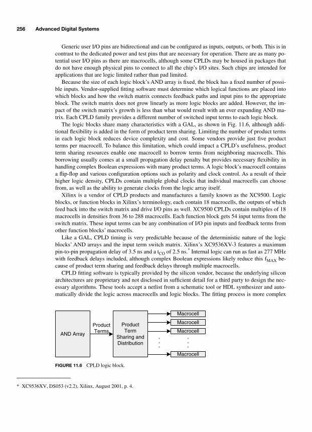
256 Advanced Digital Systems
Generic user I/O pins are bidirectional and can be configured as inputs, outputs, or both. This is incontrast to the dedicated power and test pins that are necessary for operation. There are as many po-tential user I/O pins as there are macrocells, although some CPLDs may be housed in packages thatdo not have enough physical pins to connect to all the chip’s I/O sites. Such chips are intended forapplications that are logic limited rather than pad limited.
Because the size of each logic block’s AND array is fixed, the block has a fixed number of possi-ble inputs. Vendor-supplied fitting software must determine which logical functions are placed intowhich blocks and how the switch matrix connects feedback paths and input pins to the appropriateblock. The switch matrix does not grow linearly as more logic blocks are added. However, the im-pact of the switch matrix’s growth is less than what would result with an ever expanding AND ma-trix. Each CPLD family provides a different number of switched input terms to each logic block.
The logic blocks share many characteristics with a GAL, as shown in Fig. 11.6, although addi-tional flexibility is added in the form of product term sharing. Limiting the number of product termsin each logic block reduces device complexity and cost. Some vendors provide just five productterms per macrocell. To balance this limitation, which could impact a CPLD’s usefulness, productterm sharing resources enable one macrocell to borrow terms from neighboring macrocells. Thisborrowing usually comes at a small propagation delay penalty but provides necessary flexibility inhandling complex Boolean expressions with many product terms. A logic block’s macrocell containsa flip-flop and various configuration options such as polarity and clock control. As a result of theirhigher logic density, CPLDs contain multiple global clocks that individual macrocells can choosefrom, as well as the ability to generate clocks from the logic array itself.
Xilinx is a vendor of CPLD products and manufactures a family known as the XC9500. Logicblocks, or function blocks in Xilinx’s terminology, each contain 18 macrocells, the outputs of whichfeed back into the switch matrix and drive I/O pins as well. XC9500 CPLDs contain multiples of 18macrocells in densities from 36 to 288 macrocells. Each function block gets 54 input terms from theswitch matrix. These input terms can be any combination of I/O pin inputs and feedback terms fromother function blocks’ macrocells.
Like a GAL, CPLD timing is very predictable because of the deterministic nature of the logicblocks’ AND arrays and the input term switch matrix. Xilinx’s XC9536XV-3 features a maximumpin-to-pin propagation delay of 3.5 ns and a t
CO
of 2.5 ns.
*
Internal logic can run as fast as 277 MHzwith feedback delays included, although complex Boolean expressions likely reduce this f
MAX
be-cause of product term sharing and feedback delays through multiple macrocells.
CPLD fitting software is typically provided by the silicon vendor, because the underlying siliconarchitectures are proprietary and not disclosed in sufficient detail for a third party to design the nec-essary algorithms. These tools accept a netlist from a schematic tool or HDL synthesizer and auto-matically divide the logic across macrocells and logic blocks. The fitting process is more complex
* XC9536XV, DS053 (v2.2), Xilinx, August 2001, p. 4.
AND Array
ProductTerm
Sharing andDistribution
ProductTerms
Macrocell
Macrocell
Macrocell
Macrocell
FIGURE 11.6 CPLD logic block.
-Balch.book Page 256 Thursday, May 15, 2003 3:46 PM

Programmable Logic Devices 257
than for a GAL; not every term within the CPLD can be fed to each macrocell because of the seg-mented AND array structure. Product term sharing places restrictions on neighboring macrocellswhen Boolean expressions exceed the number of product terms directly connected to each macro-cell. The fitting software first reduces the netlist to a set of Boolean expressions in the form that canbe mapped into the CPLD and then juggles the assignment of macrocells to provide each with its re-quired product terms. Desired operating frequency influences the placement of logic because of thedelay penalties of sharing product terms across macrocells. These trade-offs occur at such a lowlevel that human intervention is often impractical.
CPLDs have come to offer flexibility advantages beyond just logic implementation. As digitalsystems get more complex, logic IC supply voltages begin to proliferate. At one time, most systemsran on a single 5-V supply. This was followed by 3.3-V systems, and it is now common to find sys-tems that operate at multiple voltages such as 3.3 V, 2.5 V, 1.8 V, and 1.5 V. CPLDs invariably findthemselves designed into mixed-voltage environments for the purposes of interface conversion andbus management. To meet these needs, many CPLDs support more than one I/O voltage standard onthe same chip at the same time. I/O pins are typically divided into banks, and each bank can be inde-pendently selected for a different I/O voltage.
Most CPLDs are relatively small in logic capacity because of the desire for very high-speed oper-ation with deterministic timing and fitting characteristics at a reasonable cost. However, someCPLDs have been developed far beyond the size of typical CPLDs. Cypress Semiconductor’sDelta39K200 contains 3,072 macrocells with several hundred kilobits of user-configurable RAM.
*
The architecture is built around clusters of 128 macrocell logic groups, each of which is similar innature to a conventional CPLD. In a similar way that CPLDs add an additional hierarchical connec-tivity layer on top of multiple GAL-type logic blocks, Cypress has added a layer on top of multipleCPLD-type blocks. Such large CPLDs may have substantial benefits for certain applications. Be-yond several hundred macrocells, however, engineers have tended to use larger and more scalableFPGA technologies.
11.4 FPGAS
CPLDs are well suited to applications involving control logic, basic state machines, and smallgroups of read/write registers. These control path applications typically require a small number offlops. Once a task requires many hundreds or thousands of flops, CPLDs rapidly become impracticalto use. Complex applications that manipulate and parse streams of data often require large quantitiesof flops to serve as pipeline registers, temporary data storage registers, wide counters, and large statemachine vectors. Integrated memory blocks are critical to applications that require multiple FIFOsand data storage buffers.
Field programmable gate arrays
(FPGAs) directly address these data pathapplications.
FPGAs are available in many permutations with varying feature sets. However, their common de-fining attribute is a fine-grained architecture consisting of an array of small logic cells, each consist-ing of a flop, a small lookup table (LUT), and some supporting logic to accelerate common functionssuch as multiplexing and arithmetic carry terms for adders and counters. Boolean expressions areevaluated by the LUTs, which are usually implemented as small SRAM arrays. Any function of fourvariables, for example, can be implemented in a 16
×
1 SRAM when the four variables serve as theindex into the memory. There are no AND/OR arrays as in a CPLD or GAL. All Boolean functions
* Delta39K ISR CPLD Family, Document #38-03039 Rev. *.C, Cypress Semiconductor, December 2001, p. 1.
-Balch.book Page 257 Thursday, May 15, 2003 3:46 PM

258 Advanced Digital Systems
are implemented within the logic cells. The cells are arranged on a grid of routing resources that canmake connections between arbitrary cells to build logic paths as shown in Fig. 11.7. Depending onthe FPGA type, special-purpose structures are placed into the array. Most often, these are config-urable RAM blocks and clock distribution elements. Around the periphery of the chip are the I/Ocells, which commonly contain one or more flops to enable high-performance synchronous inter-faces. Locating flops within I/O cells improves timing characteristics by minimizing the distance,and hence the delay between each flop and its associated pin. Unlike CPLDs, most FPGAs are basedon SRAM technology, making their configurations volatile. A typical FPGA must be reprogrammedeach time power is applied to a system. Major vendors of FPGAs include Actel, Altera, Atmel, Lat-tice, QuickLogic, and Xilinx.
Very high logic densities are achieved by scaling the size of the two-dimensional logic cell array.The primary limiting factor in FPGA performance becomes routing because of the nondeterministicnature of a multipath grid interconnect system. Paths between logic cells can take multiple routes,some of which may provide identical propagation delays. However, routing resources are finite, andconflicts quickly arise between competing paths for the same routing channels. As with CPLDs,FPGA vendors provide proprietary software tools to convert a netlist into a final programming im-age. Depending on the complexity of the design (e.g., speed and density), routing an FPGA can takea few minutes or many hours. Unlike a CPLD with deterministic interconnection resources, FPGAtiming can vary dramatically, depending on the quality of the logic placement. Large, fast designs re-quire iterative routing and placement algorithms.
RoutingResources
LC LC
LC LC LC
LC LC LC LC
LC LC LC LC
LC
LC
LC
LC
RAM
LC LC LC LC LC
RAM
IO IO IO IO IO
IO
IO
IO
IO
IO IO IO IO IO IO
IO
IO
IO
IO
IO
IO
LC LC
LC
IO
Logic Paths
FIGURE 11.7 FPGA logic cell array.
-Balch.book Page 258 Thursday, May 15, 2003 3:46 PM
Programmable Logic Devices 259
Human intervention can be critical to the successful routing and timing of a complex FPGA de-sign.
Floorplanning
is the process by which an engineer manually partitions logic into groups andthen explicitly places these groups into sections of the logic cell array. Manually locating large por-tions of the logic restricts the routing software to optimizing placement of logic within those bound-aries and reduces the number of permutations that it must try to achieve a successful result.
Each vendor’s logic cell architecture differs somewhat, but mainly in how support functions suchas multiplexing and arithmetic carry terms are implemented. For the most part, engineers do nothave to consider the minute details of each logic cell structure, because the conversion of logic intothe logic cell is performed by a combination of the HDL synthesis tool and the vendor’s proprietarymapping software. In extreme situations, wherein a very specific logic implementation is necessaryto squeeze the absolute maximum performance from a specific FPGA, optimizing logic and archi-tecture for a given logic cell structure may have benefits. Engaging in this level of technology-spe-cific optimization, however, can be very tricky and lead to a house-of-cards scenario in whicheverything is perfectly balanced for a while, and then one new feature is added that upsets the wholeplan. If a design appears to be so aggressive as to require fine-tuned optimization, and faster devicescannot be obtained, it may be preferable to modify the architecture to enable more mainstream, ab-stracted design methodologies.
Notwithstanding the preceding comments, there are high-level feature differences among FPGAsthat should be evaluated before choosing a specific device. Of course, it is necessary to pick anFPGA that has sufficient logic and I/O pins to satisfy the needs of the intended application. But notall FPGAs are created equal, despite having similar quantities of logic. While the benefits of onelogic structure over another can be debated, the presence or absence of critical design resources canmake implementation of a specific design possible or impossible. These resources are clock distribu-tion elements, embedded memory, embedded third-party cores, and multifunction I/O cells.
Clock distribution across a synchronous system must be done with minimal skew to achieve ac-ceptable timing. Each logic cell within a FPGA holds a flop that requires a clock. Therefore, anFPGA must provide at least one global clock signal distributed to each logic cell with low skewacross the entire device. One clock is insufficient for most large digital systems because of the prolif-eration of different interfaces, microprocessors, and peripherals. Typical FPGAs provide anywherefrom 4 to 16 global clocks with associated low-skew distribution resources. Most FPGAs do allowclocks to be routed using the general routing resources that normally carry logic signals. However,these paths are usually unable to achieve the low skew characteristics of the dedicated clock distribu-tion network and, consequently, do not enable high clock speeds.
Some FPGAs support a large number of clocks, but with the restriction that not all clocks can beused simultaneously in the same portion of the chip. This type of restriction reduces the complexityof clock distribution on the part of the FPGA vendor because, while the entire chip supports a largenumber of clocks in total, individual sections of the chip support a smaller number. For example, anFPGA might support 16 global clocks with the restriction that any one quadrant can support only 8clocks. This means that there are 16 clocks available, and each quadrant can select half of them forarbitrary use. Instead of providing 16 clocks to each logic cell, only 8 need be connected, thus sim-plifying the FPGA circuitry.
Most FPGAs provide
phase locked loops
(PLLs) or
delay locked loops
(DLLs) that enable the in-tentional skewing, division, and multiplication of incoming clock signals. PLLs are partially analogcircuits, whereas DLLs are fully digital circuits. They have significant overlap in the functions thatthey can provide in an FPGA, although engineers may debate the merits of one versus the other. Thefundamental advantage of a PLL or DLL within an FPGA is its ability to improve I/O timing (e.g.,t
CO
) by effectively removing the propagation delay between the clock input pin and the signal outputpin, also known as
deskewing
. As shown in Fig. 11.8, the PLL or DLL aligns the incoming clock toa feedback clock with the same delay as observed at the I/O flops. In doing so, it shifts the incoming
-Balch.book Page 259 Thursday, May 15, 2003 3:46 PM
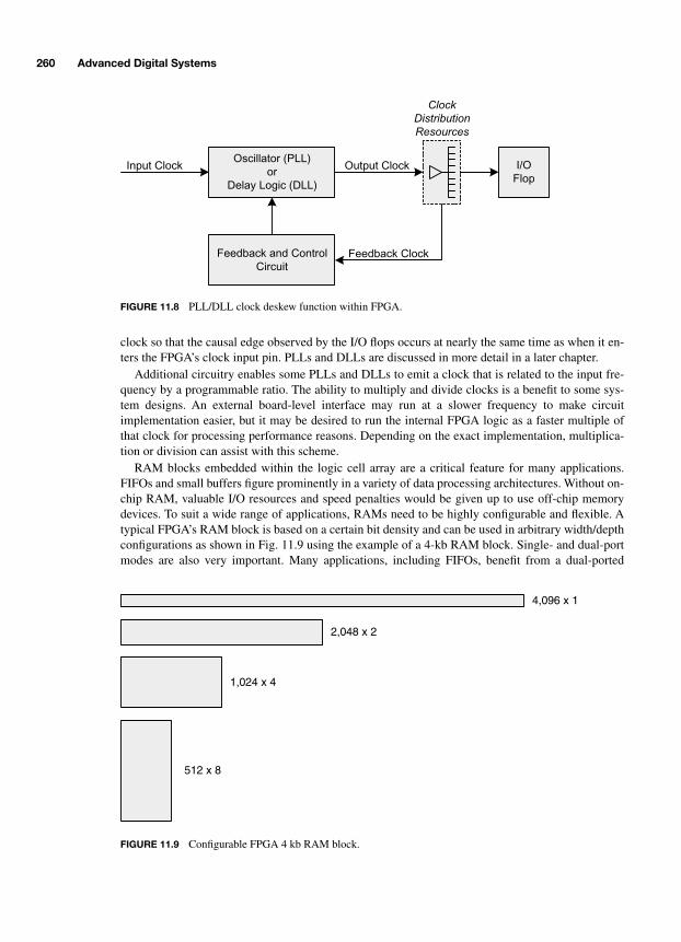
260 Advanced Digital Systems
clock so that the causal edge observed by the I/O flops occurs at nearly the same time as when it en-ters the FPGA’s clock input pin. PLLs and DLLs are discussed in more detail in a later chapter.
Additional circuitry enables some PLLs and DLLs to emit a clock that is related to the input fre-quency by a programmable ratio. The ability to multiply and divide clocks is a benefit to some sys-tem designs. An external board-level interface may run at a slower frequency to make circuitimplementation easier, but it may be desired to run the internal FPGA logic as a faster multiple ofthat clock for processing performance reasons. Depending on the exact implementation, multiplica-tion or division can assist with this scheme.
RAM blocks embedded within the logic cell array are a critical feature for many applications.FIFOs and small buffers figure prominently in a variety of data processing architectures. Without on-chip RAM, valuable I/O resources and speed penalties would be given up to use off-chip memorydevices. To suit a wide range of applications, RAMs need to be highly configurable and flexible. Atypical FPGA’s RAM block is based on a certain bit density and can be used in arbitrary width/depthconfigurations as shown in Fig. 11.9 using the example of a 4-kb RAM block. Single- and dual-portmodes are also very important. Many applications, including FIFOs, benefit from a dual-ported
Oscillator (PLL)
or
Delay Logic (DLL)
Input Clock Output Clock
Feedback and Control
Circuit
Feedback Clock
ClockDistributionResources
I/O
Flop
FIGURE 11.8 PLL/DLL clock deskew function within FPGA.
4,096 x 1
2,048 x 2
1,024 x 4
512 x 8
FIGURE 11.9 Configurable FPGA 4 kb RAM block.
-Balch.book Page 260 Thursday, May 15, 2003 3:46 PM
Programmable Logic Devices 261
RAM block to enable simultaneous reading and writing of the memory by different logic blocks.One state machine may be writing data into a RAM, and another may be reading other data out at thesame time. RAM blocks can have synchronous or asynchronous interfaces and may support one ortwo clocks in synchronous modes. Supporting two clocks in synchronous modes facilitates dual-clock FIFO designs for moving data between different clock domains.
Some FPGAs also allow logic cell LUTs to be used as general RAM in certain configurations. A16
×
1 four-input LUT can serve as a 16
×
1 RAM if supported by the FPGA architecture. It is moreefficient to use RAM blocks for large memory structures, because the hardware is optimized to pro-vide a substantial quantity of memory in a small area of silicon. However, LUT-based RAM is bene-ficial when a design requires many shallow memory structures (e.g., a small FIFO) and all the largeRAM blocks are already used. Along with control logic, 32 four-input LUTs can be used to con-struct a 16
×
32 FIFO. If a design is memory intensive, it could be wasteful to commit one or morelarge RAM blocks for such a small FIFO.
Embedding third-party logic cores is a feature that can be useful for some designs, and not usefulat all for others. A disadvantage of FPGAs is their higher cost per gate than custom ASIC technol-ogy. The main reason that engineers are willing to pay this cost premium is for the ability to imple-ment custom logic in a low-risk development process. Some applications involve a mix of customand predesigned logic that can be purchased from a third party. Examples of this include buying amicroprocessor design or a standard bus controller (e.g., PCI) and integrating it with custom logic onthe same chip. Ordinarily, the cost per gate of the third-party logic would be the same as that of yourcustom logic. On top of that cost is the licensing fee charged by the third party. Some FPGA vendorshave decided that there is sufficient demand for a few standard logic cores to offer specific FPGAsthat embed these cores into the silicon in a fixed configuration. The benefit of doing so is to drop theper-gate cost of the core to nearly that of a custom ASIC, because the core is hard wired and requiresnone of the FPGA’s configuration overhead.
FPGAs with embedded logic cores may cost more to offset the licensing costs of the cores, butthe idea is that the overall cost to the customer will be reduced through the efficiency of the hard-wired core implementation. Microprocessors, PCI bus controllers, and high-speed serdes compo-nents are common examples of FPGA embedded cores. Some specific applications may be wellsuited to this concept.
I/O cell architecture can have a significant impact on the types of board-level interfaces that theFPGA can support. The issues revolve around two variables: synchronous functionality and voltage/current levels. FPGAs support generic I/O cells that can be configured for input-only, output-only,or bidirectional operation with associated tri-state buffer output enable capability. To achieve thebest I/O timing, flops for all three functions—input, output, and output-enable—should be includedwithin the I/O cell as shown in Fig. 11.10. The timing improvement obtained by locating these threeflops in the I/O cells is substantial. The alternative would be to use logic cell flops and route pathsfrom the logic cell array directly to the I/O pin circuitry, increasing the I/O delay times. Each of thethree I/O functions is provided in both registered and unregistered options using multiplexers toprovide complete flexibility in logic implementation.
More advanced bus interfaces run at double data rate speeds, requiring more advanced I/O cellstructures to achieve the necessary timing specifications. Newer FPGAs are available with I/O cellsthat specifically support DDR interfaces by incorporating two sets of flops, one for each clock edgeas shown in Fig. 11.11. When configured for DDR mode, each of the three I/O functions is driven bya pair of flops, and a multiplexer selects the appropriate flop output depending on the phase of theclock. A DDR interface runs externally to the FPGA on both edges of the clock with a certain width.Internally, the interface runs at double the external width on only one edge of the same clock fre-quency. Therefore, the I/O cell serves as a 2:1 multiplexer for outputs and a 1:2 demultiplexer for in-puts when operating in DDR mode.
-Balch.book Page 261 Thursday, May 15, 2003 3:46 PM

262 Advanced Digital Systems
OutputEnable
I/OPin
D Q
OutputData
ConfigurationInformation
InputData DQ
D Q
FIGURE 11.10 FPGA I/O cell structure.
DDR
D Q
ConfigurationInformation
OutputEnable
#2
DDR Mux Control(e.g. Clock Phase)
InputData#1
OutputEnable
#1
I/OPin
OutputData
#1, #2
InputData#2
DQ
DQ
D Q
FIGURE 11.11 FPGA DDR I/O cell structure.
-Balch.book Page 262 Thursday, May 15, 2003 3:46 PM

Programmable Logic Devices 263
Aside from synchronous functionality, compliance with various I/O voltage and current drivestandards is a key feature for modern, flexible FPGAs. Like CPLDs that support multiple I/O banks,each of which that can drive a different voltage level, FPGAs are usually partitioned into I/O banksas well, for the same purpose. In contrast with CPLDs, many FPGAs support a wider variety of I/Ostandards for greater design flexibility.
-Balch.book Page 263 Thursday, May 15, 2003 3:46 PM

This page intentionally left blank.

P R TA 3
ANALOG BASICS FOR DIGITAL SYSTEMS
-Balch.book Page 265 Thursday, May 15, 2003 3:46 PM
Copyright 2003 by The McGraw-Hill Companies, Inc. Click Here for Terms of Use.

This page intentionally left blank.
267
CHAPTER 12
Electrical Fundamentals
It is easy to forget that digital systems are really large collections of analog electrical circuits beingoperated in a digital manner. It is easy to forget this until the digital components need to be con-nected to adequate power supplies, until digital circuits experience noise problems, and until digitalsystems need to exchange stimulus and control with our analog world. An understanding of basiccircuit theory and a working knowledge of fundamental analog principles provide a digital engineerwith confidence and the ability to design a system that will work reliably at the end of the day.
This chapter begins to peel back the veil of analog circuit theory by starting with the basics ofOhm’s law, units of measure, and basic circuit analysis techniques. After presenting DC circuitscomposed of resistors and capacitors, the discussion moves on to frequency-domain analysis and ACcircuits. These topics are presented with a minimum of mathematical complexity, because the goal isto support a digital system rather than focusing on analog signal processing. Filters are introduced inthe second half of the chapter. Relatively simple filters are common in digital systems, partly be-cause of the need to reduce noise so that more sensitive components such as oscillators and interfaceICs can operate properly.
Constructing digital systems in a reliable manner requires a foundation in analog circuit behavior,and the remainder of this book assumes a basic knowledge of circuit theory that is covered in thischapter. Some or all of the topics presented here may be a review for some readers. A quick skim ofthe chapter’s material will confirm whether it can be skipped.
12.1 BASIC CIRCUITS
Electric potential, called
voltage
, and current are the two basic parameters used in the analysis ofelectric circuits. Voltage is measured in
volts,
and current is measured in
amperes
, or
amps
. Usingthe analogy of a hose filled with water, voltage is akin to the water’s pressure, and current is akin tothe quantity of water flowing through the hose at a given pressure. Unlike water in a hose, electricityonly flows when a complete loop, or
circuit
, is present. Electric charge (expressed in units of cou-lombs) is emitted from one terminal of a power source, flows through a circuit, and then returns inthe same quantity to another terminal of that power source. Per the law of conservation of charge,the charge cannot simply disappear in the circuit; it must return to its source to complete the loop.
Georg Ohm, a nineteenth century German physicist, discovered the mathematical relationship be-tween voltage and current that is now known as Ohm’s law:
V
=
IR
. It states that a voltage
(V)
dropresults by passing a current
(I)
through a resistance
(R)
. Appropriately, the unit of resistance is the
ohm
and it is represented with the Greek letter omega,
Ω
. Consider the simple circuit in Fig. 12.1,consisting of a 10-V battery and a 50-
Ω
resistor. Assuming that the connecting wires have zero resis-tance, there is one and only one solution to Ohm’s law: the current through the circuit is
I
=
V
÷
R
=
-Balch.book Page 267 Thursday, May 15, 2003 3:46 PM
Copyright 2003 by The McGraw-Hill Companies, Inc. Click Here for Terms of Use.

268 Analog Basics for Digital Systems
10 ÷ 50 = 0.2 A, or 200 mA. If any of the wires are broken, the current flow instantly drops to zero,because charge cannot return to the battery. Remember that all circuits are a collection of loops. Mak-ing and breaking loops using switches (transistors) is fundamentally how digital systems operate.
Voltage is a relative measurement, and its effects can be quantified only between pairs of conduc-tors. This is why a bird can sit on a high-voltage power line without being electrocuted and why aperson can walk around on a carpet while insulated from nearby conductors and develop a high volt-age static electric charge of several thousand volts. Not until the conductor (e.g., bird or person)comes into contact with another conductor (e.g., another wire or a metal door handle) does the effectof voltage become apparent. To facilitate circuit analysis, a common reference point called a
ground
node is assigned a relative voltage of zero. The ground symbol is shown attached to the battery’snegative terminal in Fig. 12.1. All other nodes in the circuit can now be measured relative to ground,resulting in meaningful absolute voltage levels. This is why electrical communication signals be-tween systems require either a common ground or a differential signaling scheme. A receiver cannotproperly detect the voltage on a signal wire unless it has a valid reference to compare it against.
An important parameter derived from Ohm’s law is power, expressed in
watts
(W). Power (P) isthe product of current and voltage. In this simple circuit, 10 V is dropped through the circuit (all bythe resistor) at a current of 0.2 A, yielding 2 W of power supplied by the battery and dissipated bythe resistor. Power is an instantaneous measurement and is not energy, but the rate of flow of energy.Energy (E) is measured in
Joules
and is the product of how much power is delivered over a span oftime:
E
=
Pt
. The resistor in this circuit converts 2 J of energy each second into heat. Per the first lawof thermodynamics, energy cannot be created or destroyed. Therefore, electrical energy that is dissi-pated by a component is converted into thermal energy. The charge still returns to the battery, but itdoes so at a relative potential of 0 V. A circuit is typically characterized by its power dissipation(watts) rather than by its energy dissipation (joules) because of the time invariant nature of power.
Power can be restated depending on the unknown variable in the equation.
P
=
VI
can be manipu-lated using Ohm’s law in several common forms:
P
=
I
2
R
and
P
=
V
2
÷
R
. In the first instance, the
V
=
IR
definition is substituted to yield a power calculation that only considers the current passingthrough a resistance. Alternatively, current can be effectively removed (
I
=
V
÷
R
), and power can berestated as the square of the voltage developed across a resistance.
12.2 LOOP AND NODE ANALYSIS
The example in Fig. 12.1 is a basic application of
loop analysis
. Loop analysis is based on the rulesthat the sum of the voltage drops in any continuous circuit is 0 and that the instantaneous currentaround the loop is constant. Of course, current can change over time, and those changes apply to eachcomponent in the circuit. Based on these rules, the following general loop equation can be written forany circuit, where
R
N
are discrete resistors and
VS
N
are discrete voltage sources (e.g., a battery):
50 Ω
10 V0.2 A
FIGURE 12.1 Simple resistive circuit.
-Balch.book Page 268 Thursday, May 15, 2003 3:46 PM
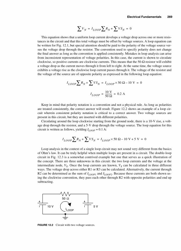
Electrical Fundamentals 269
This equation shows that a uniform loop current develops a voltage drop across one or more resis-tances in the circuit and that this total voltage must be offset by voltage sources. A loop equation canbe written for Fig. 12.1, but special attention should be paid to the polarity of the voltage source ver-sus the voltage drop through the resistor. The convention used to specify polarity does not changethe final answer as long as the convention is applied consistently. Mistakes in loop analysis can arisefrom inconsistent representation of voltage polarities. In this case, the current is shown to circulateclockwise, so positive currents are clockwise currents. This means that the 50-
Ω
resistor will exhibita voltage drop as the current moves through it from left to right. At the same time, the voltage sourceexhibits a voltage rise as the clockwise loop current passes through it. The voltage of the resistor andthe voltage of the source are of opposite polarity as expressed in the following loop equation:
Keep in mind that polarity notation is a convention and not a physical rule. As long as polaritiesare treated consistently, the correct answer will result. Figure 12.2 shows an example of a loop cir-cuit wherein consistent polarity notation is critical to a correct answer. Two voltage sources arepresent in this circuit, but they are inserted with different polarities.
Circulating around the loop clockwise starting from the ground node, there is a 10-V rise, a volt-age drop through the resistor, and a 5-V drop through the voltage source. The loop equation for thiscircuit is written as follows, yielding
I
LOOP
= 0.1 A:
Loop analysis in the context of a single loop circuit may not sound very different from the basicsof Ohm’s law. It can be truly helpful when multiple loops are present in a circuit. The double-loopcircuit in Fig. 12.3 is a somewhat contrived example but one that serves as a quick illustration ofthe concept. There are three unknowns in this circuit: the two loop currents and the voltage at theintermediate node,
V
X
. Once the loop currents are known,
V
X
can be calculated in three differentways. The voltage drop across either R1 or R3 can be calculated. Alternatively, the current throughR2 can be determined as the sum of
I
LOOP
1
and
I
LOOP
2
. Because these currents are both shown us-ing the clockwise convention, they pass each other through R2 with opposite polarities and end upsubtracting.
V N∑ ILOOP RN V SN∑+∑ 0= =
ILOOP10 V50 Ω------------ 0.2 A= =
ILOOP RN V SN∑+∑ ILOOP 50 Ω 10 V–× 0= =
50 Ω
10 VILOOP
5 V
FIGURE 12.2 Circuit with two voltage sources.
ILOOP RN V SN∑+∑ ILOOP 50 Ω 10 V 5 V+–× 0= =
-Balch.book Page 269 Thursday, May 15, 2003 3:46 PM
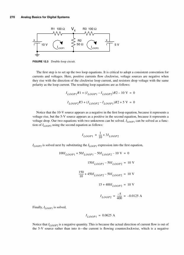
270 Analog Basics for Digital Systems
The first step is to set up the two loop equations. It is critical to adopt a consistent convention forcurrents and voltages. Here, positive currents flow clockwise, voltage sources are negative whenthey rise with the direction of the clockwise loop current, and resistors drop voltage with the samepolarity as the loop current. The resulting loop equations are as follows:
Notice that the 10-V source appears as a negative in the first loop equation, because it represents avoltage rise, but the 5-V source appears as a positive in the second equation, because it represents avoltage drop. Our two equations with two unknowns can be solved.
I
LOOP
1
can be solved as a func-tion of
I
LOOP
2
using the second equation as follows:
I
LOOP
2
is solved next by substituting the
I
LOOP
1
expression into the first equation,
Finally,
I
LOOP
1
is solved,
Notice that
I
LOOP
2
is a negative quantity. This is because the actual direction of current flow is out ofthe 5-V source rather than into it—the current is flowing counterclockwise, which is a negative
R1 100 Ω
10 VILOOP1
5 VR2
50 Ω
R3 100 Ω
ILOOP2
VX
FIGURE 12.3 Double-loop circuit.
ILOOP1R1 ILOOP1 ILOOP2–( )R2 10 V–+ 0=
ILOOP2R3 ILOOP2 ILOOP1–( )R2 5 V+ + 0=
ILOOP11
10------ 3ILOOP2+=
100ILOOP1 50ILOOP1 50ILOOP2 10 V––+ 0=
150ILOOP1 50ILOOP2– 10 V=
15010
--------- 450ILOOP2 50ILOOP2–+ 10 V=
15 400ILOOP2+ 10 V=
ILOOP25–
400--------- 0.0125 A–= =
ILOOP1 0.0625 A=
-Balch.book Page 270 Thursday, May 15, 2003 3:46 PM

Electrical Fundamentals 271
clockwise current. Our results can be verified to make sure that everything adds up correctly. Thevoltage drops across R1 and R3 are 6.25 V and 1.25 V, respectively. Therefore, VX = 10 V – 6.25 V =5 V – 1.25 V = 3.75 V. This means that the current through R3 must be 3.75 V ÷ 50 Ω = 0.075 A,which is exactly equal to the difference of the two loop currents (IR2 = ILOOP1 – ILOOP2).
Node analysis is the complement to loop analysis. Rather than dealing with a fixed current arounda loop in which the voltages sum to zero, node analysis examines an individual node with a fixedvoltage where the currents sum to zero. Together, these loop and node analysis methods form the ba-sis of circuit analysis. You may find that some circuits are more easily solved with one or the other.As before, the consistent usage of a polarity convention is critical to finding the correct answer. Thecircuit in Fig. 12.3 can be evaluated with just one node equation to determine VX. In the followingequation, the convention is taken that positive currents flow out of the node.
This node equation does not worry about whether VX is actually higher or lower than the voltage atthe other end of each resistor. If current is actually flowing into the node because the reverse voltagerelationship is true, that current will have a negative polarity. Working through the algebra showsthat VX = 3.75 V, the same answer that was obtained using loop analysis, although with only a singleequation and one unknown. If the current through any resistor must be calculated, it can be doneonce VX is known.
12.3 RESISTANCE COMBINATION
Circuits can be simplified for analysis purposes when multiple resistances are present in various se-ries and parallel topologies. Multiple resistors can be combined in arbitrary configurations and rep-resented as a single resistance. Two resistors placed in series add, while resistors placed in parallelresult in a smaller overall resistance. Resistors in parallel create a combined resistance that is lessthan the smallest valued resistor in the parallel group. This resulting value is determined using theinverse relationship,
Multiple resistors placed in parallel can be indicated using a parallel bar notation. indi-cates that two resistors, referred to as R1 and R2, are in parallel. When two resistors are placed in aparallel arrangement, the above expression can be rewritten for this special circumstance:
Figure 12.4 shows resistors in both series and parallel topologies. Series resistors R1 and R2 addto form a 150-Ω resistance. Parallel resistors R3 and R4 combine to form a smaller 33.3-Ω resis-tance. Placing two resistors back to back increases the total resistance observed by a current. Placingtwo resistors in parallel provides a second path for current to flow through, thereby reducing theoverall resistance. After performing these two combinations, the circuit can be simplified a thirdtime by adding the resulting series resistances, 150 Ω + 33.3 Ω = 183.3 Ω. When the circuit has been
0 IN∑V X 10 V–
R1--------------------------
V X 0 V–
R2----------------------
V X 5 V–
R3----------------------+ += =
RTOTAL1
1RN-------∑
----------------=
R1 R2||
RTOTALR1 R2×R1 R2+--------------------=
-Balch.book Page 271 Thursday, May 15, 2003 3:46 PM
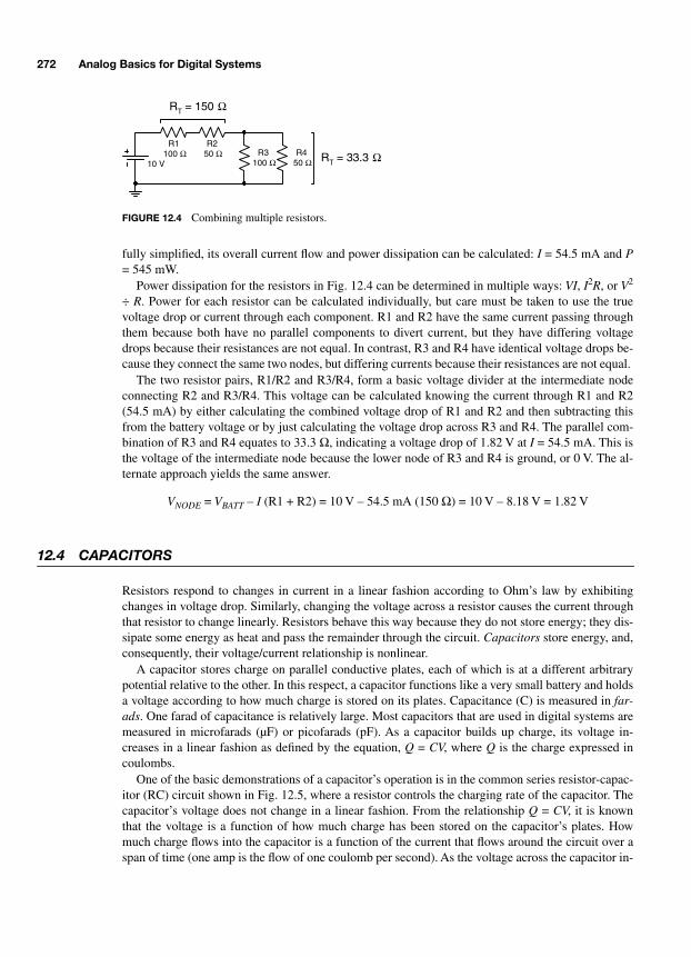
272 Analog Basics for Digital Systems
fully simplified, its overall current flow and power dissipation can be calculated: I = 54.5 mA and P= 545 mW.
Power dissipation for the resistors in Fig. 12.4 can be determined in multiple ways: VI, I2R, or V2
÷ R. Power for each resistor can be calculated individually, but care must be taken to use the truevoltage drop or current through each component. R1 and R2 have the same current passing throughthem because both have no parallel components to divert current, but they have differing voltagedrops because their resistances are not equal. In contrast, R3 and R4 have identical voltage drops be-cause they connect the same two nodes, but differing currents because their resistances are not equal.
The two resistor pairs, R1/R2 and R3/R4, form a basic voltage divider at the intermediate nodeconnecting R2 and R3/R4. This voltage can be calculated knowing the current through R1 and R2(54.5 mA) by either calculating the combined voltage drop of R1 and R2 and then subtracting thisfrom the battery voltage or by just calculating the voltage drop across R3 and R4. The parallel com-bination of R3 and R4 equates to 33.3 Ω, indicating a voltage drop of 1.82 V at I = 54.5 mA. This isthe voltage of the intermediate node because the lower node of R3 and R4 is ground, or 0 V. The al-ternate approach yields the same answer.
VNODE = VBATT – I (R1 + R2) = 10 V – 54.5 mA (150 Ω) = 10 V – 8.18 V = 1.82 V
12.4 CAPACITORS
Resistors respond to changes in current in a linear fashion according to Ohm’s law by exhibitingchanges in voltage drop. Similarly, changing the voltage across a resistor causes the current throughthat resistor to change linearly. Resistors behave this way because they do not store energy; they dis-sipate some energy as heat and pass the remainder through the circuit. Capacitors store energy, and,consequently, their voltage/current relationship is nonlinear.
A capacitor stores charge on parallel conductive plates, each of which is at a different arbitrarypotential relative to the other. In this respect, a capacitor functions like a very small battery and holdsa voltage according to how much charge is stored on its plates. Capacitance (C) is measured in far-ads. One farad of capacitance is relatively large. Most capacitors that are used in digital systems aremeasured in microfarads (µF) or picofarads (pF). As a capacitor builds up charge, its voltage in-creases in a linear fashion as defined by the equation, Q = CV, where Q is the charge expressed incoulombs.
One of the basic demonstrations of a capacitor’s operation is in the common series resistor-capac-itor (RC) circuit shown in Fig. 12.5, where a resistor controls the charging rate of the capacitor. Thecapacitor’s voltage does not change in a linear fashion. From the relationship Q = CV, it is knownthat the voltage is a function of how much charge has been stored on the capacitor’s plates. Howmuch charge flows into the capacitor is a function of the current that flows around the circuit over aspan of time (one amp is the flow of one coulomb per second). As the voltage across the capacitor in-
R1100 Ω
10 V
R250 Ω
RT = 150 Ω
R3100 Ω
R450 Ω RT = 33.3 Ω
FIGURE 12.4 Combining multiple resistors.
-Balch.book Page 272 Thursday, May 15, 2003 3:46 PM
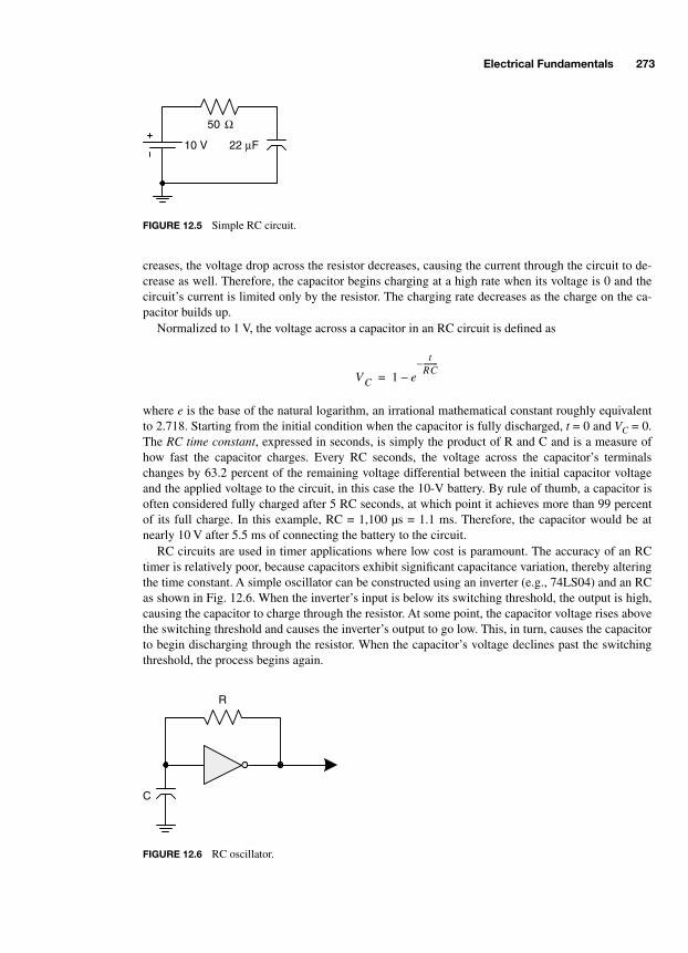
Electrical Fundamentals 273
creases, the voltage drop across the resistor decreases, causing the current through the circuit to de-crease as well. Therefore, the capacitor begins charging at a high rate when its voltage is 0 and thecircuit’s current is limited only by the resistor. The charging rate decreases as the charge on the ca-pacitor builds up.
Normalized to 1 V, the voltage across a capacitor in an RC circuit is defined as
where e is the base of the natural logarithm, an irrational mathematical constant roughly equivalentto 2.718. Starting from the initial condition when the capacitor is fully discharged, t = 0 and VC = 0.The RC time constant, expressed in seconds, is simply the product of R and C and is a measure ofhow fast the capacitor charges. Every RC seconds, the voltage across the capacitor’s terminalschanges by 63.2 percent of the remaining voltage differential between the initial capacitor voltageand the applied voltage to the circuit, in this case the 10-V battery. By rule of thumb, a capacitor isoften considered fully charged after 5 RC seconds, at which point it achieves more than 99 percentof its full charge. In this example, RC = 1,100 µs = 1.1 ms. Therefore, the capacitor would be atnearly 10 V after 5.5 ms of connecting the battery to the circuit.
RC circuits are used in timer applications where low cost is paramount. The accuracy of an RCtimer is relatively poor, because capacitors exhibit significant capacitance variation, thereby alteringthe time constant. A simple oscillator can be constructed using an inverter (e.g., 74LS04) and an RCas shown in Fig. 12.6. When the inverter’s input is below its switching threshold, the output is high,causing the capacitor to charge through the resistor. At some point, the capacitor voltage rises abovethe switching threshold and causes the inverter’s output to go low. This, in turn, causes the capacitorto begin discharging through the resistor. When the capacitor’s voltage declines past the switchingthreshold, the process begins again.
50 Ω
10 V 22 µF
FIGURE 12.5 Simple RC circuit.
V C 1 e
tRC--------–
–=
R
C
FIGURE 12.6 RC oscillator.
-Balch.book Page 273 Thursday, May 15, 2003 3:46 PM

274 Analog Basics for Digital Systems
In reality, the inverter does not switch sharply as the input voltage slowly passes out of the validlogic-0 and logic-1 voltage thresholds. This creates a separate switching threshold when going fromlow to high versus high to low. The voltage difference between these thresholds depends on temper-ature, the operating voltage, and the individual chip’s characteristics. Therefore, a simple inverter-based oscillator does not provide a very stable oscillation period over time without additional cir-cuitry. The waveform in Fig. 12.7 shows how this RC oscillator behaves.
This waveform shows the nonlinear charging characteristics of an RC circuit. The frequency atwhich this oscillator runs depends on the differential between the two switching thresholds, the inputcurrent of the inverter, and the RC values. The ideal RC charge/discharge curve is modified by theinverter’s input current. When the capacitor is at logic-1, the positive input (sink) current of the in-verter works with the resistor to more rapidly discharge the capacitor. Similarly, when the capacitoris at logic-0, the negative input (source) current of the inverter works with the resistor to more rap-idly charge the capacitor. These source and sink currents are unequal in a bipolar logic IC; therefore,the charge/discharge effects of the inverter will be unequal as well.
12.5 CAPACITORS AS AC ELEMENTS
Capacitors have a far broader range of applications than just RC oscillators. The circuits presentedup to this point are direct current (DC) circuits. In our context, DC refers to steady-state signals withno frequency content being applied to a circuit. While the RC oscillator example certainly varies itsvoltages, it is a piecewise DC circuit that flips its applied charging voltage at regular intervals. Theworld is not static, however, and signals are characterized by direct and alternating current (AC)components. AC circuits deal with the time-varying properties of signals, their frequency content.
Just as resistors exhibit resistance, capacitors exhibit reactance. Both measures are expressed inohms, but resistance is constant across frequency, whereas reactance (X) varies with frequency. Thetwo terms are combined into a single impedance expression, Z = R + jX. Impedance is the overall re-sistance of an element that includes both DC and AC components. The imaginary (AC) component,a function of frequency, is marked by the constant j, the imaginary number .
AC circuit analysis expresses frequencies in radians per second rather than in hertz and uses thelower-case Greek letter omega, ω, to denote radian frequency. There are 2π radians in a 360° circle,
Inverter Output High, Capacitor Charges
Inverter Output Low, Capacitor Discharges
Time
InverterInput
Voltage
Low-to-HighThreshold
High-to-LowThreshold
FIGURE 12.7 RC oscillator waveform.
1–
-Balch.book Page 274 Thursday, May 15, 2003 3:46 PM

Electrical Fundamentals 275
or cycle. Therefore, there are 2π radians per hertz, or ω = 2πf. The 2πf equivalent is primarily usedin this book to illustrate how various circuits interact with digital systems running at arbitrary fre-quencies.
The impedance of an ideal capacitor is inversely related to the frequency applied to it and is ex-pressed as
At low frequencies, the capacitor exhibits very high impedance and appears essentially as an opencircuit. Considering a basic RC circuit, once the capacitor fully charges, the circuit transitions to asteady-state DC circuit without any AC component. Therefore, no more current flows through thecircuit, because the capacitor has achieved the same voltage as the battery, and there is no voltagedrop across the charging resistor. In AC analysis terms, the frequency of the circuit is zero, and theimpedance of the capacitor is infinite. Conversely, a capacitor’s impedance asymptotically ap-proaches zero at very high frequencies and becomes a short circuit.
A capacitor can be used to reduce noise in a system, because its impedance is a function of fre-quency. Decoupling, or bypass, capacitors are arranged in shunt (parallel) configurations acrosspower supplies that may contain noise, as shown in Fig. 12.8. Power distribution wires can havenoise injected back into them by the high-speed on/off switching of a digital circuit. Each time alogic gate or flop transitions, a small surge of current is created to establish the new voltage level.When hundreds or thousands of signals within and external to an IC switch on and off, noise can be-come a substantial problem.
Decoupling capacitors can be chosen to present a low impedance at the noise frequencies of inter-est in a digital system. Lower-frequency systems often use 0.1-µF capacitors that exhibit impedanceof under 1 Ω at over 1 MHz. Higher-frequency systems may use 0.01-µF or 0.001-µF capacitors forthe same purpose. The capacitor functions as a selective resistor that only kicks in at certain frequen-cies of interest and leaves the DC signal, in this case power, undisturbed. Figure 12.9 illustrates theeffect of a decoupling capacitor in shunting the majority of the high-frequency AC component(noise) to ground. Most of the noise is removed, but some remains, as will be explained later.
Multiple capacitors arranged together follow the same series and parallel impedance calculationrule as resistors. However, because of the capacitor’s inversely proportional impedance characteris-
ZC1
2πfC-------------=
0.01 µFHigh-frequency
noise
Reducednoiseto ICs
FIGURE 12.8 Noise filtering with shunt capacitance.
DC componentof power
Volts
Time
without capacitor with capacitor
FIGURE 12.9 AC noise removed from DC power.
-Balch.book Page 275 Thursday, May 15, 2003 3:46 PM
276 Analog Basics for Digital Systems
tic, total capacitance is increased when multiple capacitors are placed in parallel and decreased whenplaced in series. Consider the following calculation for two equal values capacitors in parallel:
The resulting impedance is what would be obtained with a capacitor twice as large as each individ-ual capacitor. Similarly, capacitance is reduced as follows when two capacitors are in series:
The series impedance is what would be obtained with a capacitor half the size of each individual ca-pacitor.
12.6 INDUCTORS
An inductor, also called a choke or coil, is the other basic circuit element whose impedance changes asa function of frequency. An inductor is a coil of wire that stores energy as a magnetic field. Thestrength of a magnetic field in a coil is proportional to the current flowing through the coil. If the cur-rent flowing through an inductor changes suddenly, the existing magnetic field tends to resist thatchange. Therefore, inductors present low impedances at low frequencies and high impedances athigher frequencies, the opposite the behavior of a capacitor. Inductance (L) is measured in henries.Most inductors encountered in digital systems are measured in microhenries (µH) or nanohenries (nH).
The impedance of an ideal inductor is expressed as ZL = 2πfL, clearly showing the proportionalrelationship of frequency and impedance. In digital systems, inductance is used mainly for filteringpurposes and for analyzing the (usually unwanted) inductance of other components. All conductorsexhibit some inductance, because a magnetic field naturally develops in proportion to current flow. Astraight wire may have much less inductance than a coil, but its inductance is not zero. Such at-tributes become very important at high frequencies because of the relationship between frequencyand impedance.
Just as a capacitor can be used as a parallel element to shunt high-frequency noise, an inductorcan be used as a series element to block that noise. Because of their varying impedance, DC signalssuch as power are passed without attenuation, whereas high frequencies are met with a large imped-ance. Effective noise filters are made with both series (inductance) and shunt (capacitance) elementsas shown in Fig. 12.10. The inductance and capacitance values are chosen to be effective at the de-sired noise frequency, resulting in a large series resistance followed by a very small shunt resistance.This creates a basic voltage divider arrangement, effective only at high frequencies as intended.
Because of their proportional impedance versus frequency characteristic, inductance combines inthe same way as resistance: decreasing with parallel inductors and increasing with series inductors.
12.7 NONIDEAL RLC MODELS
Having presented the three basic passive circuit elements in idealized form, the ways in which resis-tance, capacitance, and inductance combine in real-world components can be discussed. All conduc-
ZTOTAL1
1ZN-------∑
---------------- 12πfC 2πfC+-------------------------------- 1
2πf 2C( )----------------------= = =
ZTOTAL ZN∑ 12πfC------------- 1
2πfC-------------+ 2
2πfC------------- 1
2πf 0.5C( )--------------------------= = = =
-Balch.book Page 276 Thursday, May 15, 2003 3:46 PM

Electrical Fundamentals 277
tors exhibit some series resistance and inductance, and all nearby pairs of conductors exhibit somemutual capacitance. A resistor consists of a resistive element encapsulated in some packaging mate-rial with a relatively small conductor at each end to connect the resistive element to an external cir-cuit. Depending on the type of resistor, the conductors may be wires (leaded resistor) or small piecesof metal foil (surface mount). The resistive element itself will vary in size according to its power rat-ing, material, and desired resistance. The finite lengths of the connecting leads and the resistive ele-ment each contribute a small quantity of inductance. There is also a small capacitance between theresistor’s leads. These unwanted extras are called parasitic properties, because they usually detractfrom the performance of a system rather than improving it. A resistor’s function is to provide a cer-tain resistance value in a circuit, but its physical construction results in finite parasitic inductanceand capacitance. Figure 12.11 shows a model of a nonideal resistor that enables analysis of its para-sitic properties.
Each type of resistor exhibits different magnitudes of parasitic properties. Applications at lowerfrequencies often ignore these properties, because the parasitic inductance and capacitance is negli-gible as a result of the frequency/impedance relationships of inductors and capacitors. As the fre-quencies involved increase, series inductance is generally the first problem that is encountered.Inductance is minimized in resistors that have small leads or, better yet, no leads at all, as is the casewith surface mount resistors. Inter-lead capacitance does not become a problem until frequencies getsignificantly higher.
Similarly, a capacitor exhibits parasitic resistance and inductance. The conductors that form thecapacitor have finite resistance and inductance associated with them. A nonideal model of a capaci-tor is shown in Fig. 12.12. Inductance figures into a capacitor in much the same way that it does a re-sistor. Smaller leads and components result in reduced parasitic inductance.
At high frequencies, however, the capacitor’s parasitic inductance has noticeable effects. The ear-lier example of using a capacitor to filter high-frequency noise showed that the capacitor removedmost of the noise, but not all of it. As the frequency rises, the capacitor’s impedance steadily de-creases as expected. At a certain point, however, the frequency becomes high enough to cause no-
reducednoiseto ICs
∞0
+ +
--
VINNOISE VOUTNOISE
FIGURE 12.10 Noise filtering with LC network.
FIGURE 12.11 Nonideal resistor model. FIGURE 12.12 Nonideal capacitor model.
-Balch.book Page 277 Thursday, May 15, 2003 3:46 PM
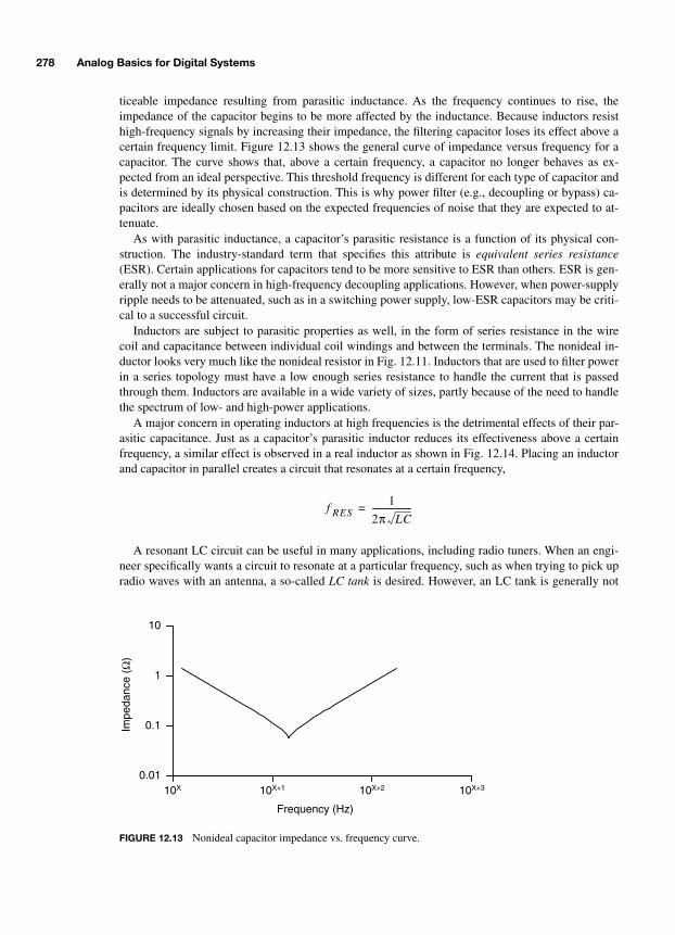
278 Analog Basics for Digital Systems
ticeable impedance resulting from parasitic inductance. As the frequency continues to rise, theimpedance of the capacitor begins to be more affected by the inductance. Because inductors resisthigh-frequency signals by increasing their impedance, the filtering capacitor loses its effect above acertain frequency limit. Figure 12.13 shows the general curve of impedance versus frequency for acapacitor. The curve shows that, above a certain frequency, a capacitor no longer behaves as ex-pected from an ideal perspective. This threshold frequency is different for each type of capacitor andis determined by its physical construction. This is why power filter (e.g., decoupling or bypass) ca-pacitors are ideally chosen based on the expected frequencies of noise that they are expected to at-tenuate.
As with parasitic inductance, a capacitor’s parasitic resistance is a function of its physical con-struction. The industry-standard term that specifies this attribute is equivalent series resistance(ESR). Certain applications for capacitors tend to be more sensitive to ESR than others. ESR is gen-erally not a major concern in high-frequency decoupling applications. However, when power-supplyripple needs to be attenuated, such as in a switching power supply, low-ESR capacitors may be criti-cal to a successful circuit.
Inductors are subject to parasitic properties as well, in the form of series resistance in the wirecoil and capacitance between individual coil windings and between the terminals. The nonideal in-ductor looks very much like the nonideal resistor in Fig. 12.11. Inductors that are used to filter powerin a series topology must have a low enough series resistance to handle the current that is passedthrough them. Inductors are available in a wide variety of sizes, partly because of the need to handlethe spectrum of low- and high-power applications.
A major concern in operating inductors at high frequencies is the detrimental effects of their par-asitic capacitance. Just as a capacitor’s parasitic inductor reduces its effectiveness above a certainfrequency, a similar effect is observed in a real inductor as shown in Fig. 12.14. Placing an inductorand capacitor in parallel creates a circuit that resonates at a certain frequency,
A resonant LC circuit can be useful in many applications, including radio tuners. When an engi-neer specifically wants a circuit to resonate at a particular frequency, such as when trying to pick upradio waves with an antenna, a so-called LC tank is desired. However, an LC tank is generally not
0.01
0.1
1
10
Impe
danc
e (Ω
)
Frequency (Hz)
10X 10X+1 10X+2 10X+3
FIGURE 12.13 Nonideal capacitor impedance vs. frequency curve.
f RES1
2π LC-------------------=
-Balch.book Page 278 Thursday, May 15, 2003 3:46 PM
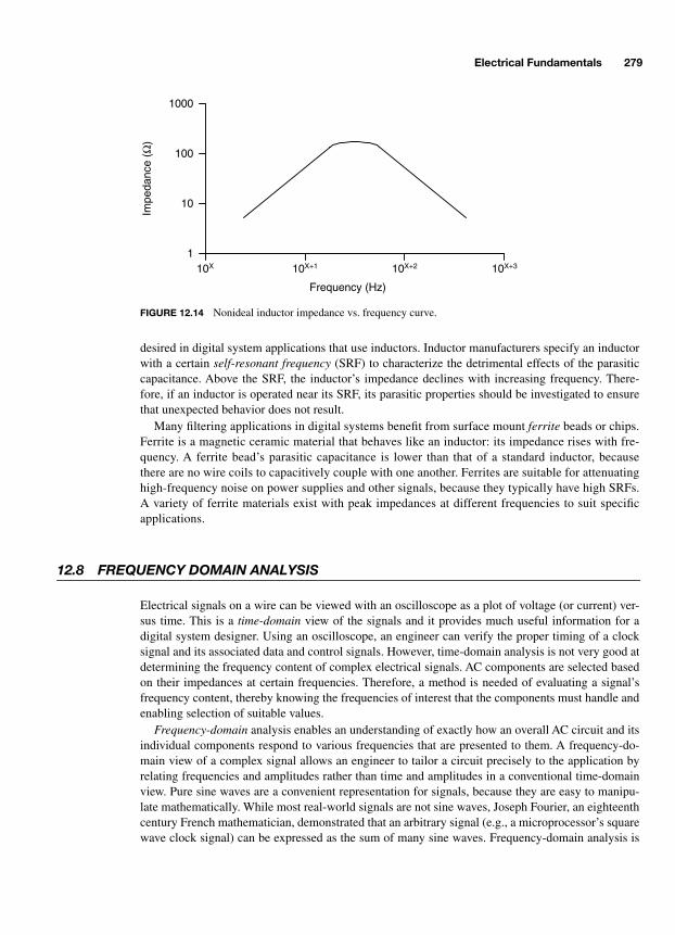
Electrical Fundamentals 279
desired in digital system applications that use inductors. Inductor manufacturers specify an inductorwith a certain self-resonant frequency (SRF) to characterize the detrimental effects of the parasiticcapacitance. Above the SRF, the inductor’s impedance declines with increasing frequency. There-fore, if an inductor is operated near its SRF, its parasitic properties should be investigated to ensurethat unexpected behavior does not result.
Many filtering applications in digital systems benefit from surface mount ferrite beads or chips.Ferrite is a magnetic ceramic material that behaves like an inductor: its impedance rises with fre-quency. A ferrite bead’s parasitic capacitance is lower than that of a standard inductor, becausethere are no wire coils to capacitively couple with one another. Ferrites are suitable for attenuatinghigh-frequency noise on power supplies and other signals, because they typically have high SRFs.A variety of ferrite materials exist with peak impedances at different frequencies to suit specificapplications.
12.8 FREQUENCY DOMAIN ANALYSIS
Electrical signals on a wire can be viewed with an oscilloscope as a plot of voltage (or current) ver-sus time. This is a time-domain view of the signals and it provides much useful information for adigital system designer. Using an oscilloscope, an engineer can verify the proper timing of a clocksignal and its associated data and control signals. However, time-domain analysis is not very good atdetermining the frequency content of complex electrical signals. AC components are selected basedon their impedances at certain frequencies. Therefore, a method is needed of evaluating a signal’sfrequency content, thereby knowing the frequencies of interest that the components must handle andenabling selection of suitable values.
Frequency-domain analysis enables an understanding of exactly how an overall AC circuit and itsindividual components respond to various frequencies that are presented to them. A frequency-do-main view of a complex signal allows an engineer to tailor a circuit precisely to the application byrelating frequencies and amplitudes rather than time and amplitudes in a conventional time-domainview. Pure sine waves are a convenient representation for signals, because they are easy to manipu-late mathematically. While most real-world signals are not sine waves, Joseph Fourier, an eighteenthcentury French mathematician, demonstrated that an arbitrary signal (e.g., a microprocessor’s squarewave clock signal) can be expressed as the sum of many sine waves. Frequency-domain analysis is
1
10
100
1000
Impe
danc
e (Ω
)
Frequency (Hz)
10X 10X+1 10X+2 10X+3
FIGURE 12.14 Nonideal inductor impedance vs. frequency curve.
-Balch.book Page 279 Thursday, May 15, 2003 3:46 PM

280 Analog Basics for Digital Systems
often referred to as Fourier analysis. Likewise, a Fourier transform is the process of decomposing asignal into a sum of sine waves.
Fourier analysis is represented graphically in Fig. 12.15, where a 1-MHz digital clock signal isshown broken into four separate sine waves. The sine wave with the same frequency as the clock isreferred to as the fundamental frequency. Subsequent sine waves are multiples of the fundamentalfrequency and are called harmonics. If a sine wave is three times the fundamental frequency, it is thethird harmonic. It is clear that, as higher-order harmonics are added to the fundamental frequency,the resulting signal looks more and more like a clock signal with square edges. This example stopsafter the seventh harmonic, but a more perfect clock signal could be constructed by continuing withhigher-frequency harmonics. From a practical perspective, it can be seen that only a few harmonicsare necessary to obtain a representation that closely approximates the real digital signal. Therefore,it is often convenient to consider the few sine wave terms that compose the majority of the signal’senergy. This simplification allows many less-significant terms to be removed from the relevant cal-culations. Depending on how accurately the digital signal really needs to be represented, it may bepossible to make a gross simplification and consider just the fundamental frequency and one or twosubsequent harmonics.
Each harmonic in a Fourier analysis has varying amplitude, frequency, and phase relationshipssuch that their sum yields the desired complex signal. The energy in harmonics generally decreasesas their frequency increases. The clock signal shown in this example has energy only at the odd har-monics, because it is a symmetrical signal. Furthermore, the harmonics are in phase with each other.More complex real-world asymmetrical signals can also be handled with Fourier analysis but withmore variation across the harmonics, including even harmonics and phase differences.
Fundamental and Third Harmonic Fundamental + Third Harmonic
+ Fifth Harmonic
+ Seventh Harmonic
Fifth Harmonic
Seventh Harmonic
FIGURE 12.15 Digital clock composed of sine waves.
-Balch.book Page 280 Thursday, May 15, 2003 3:46 PM
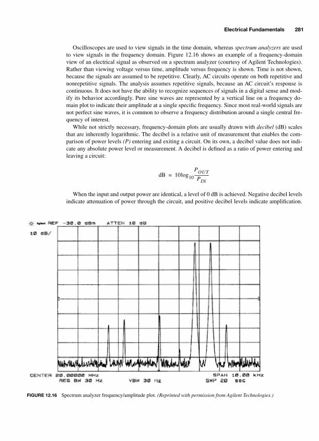
Electrical Fundamentals 281
Oscilloscopes are used to view signals in the time domain, whereas spectrum analyzers are usedto view signals in the frequency domain. Figure 12.16 shows an example of a frequency-domainview of an electrical signal as observed on a spectrum analyzer (courtesy of Agilent Technologies).Rather than viewing voltage versus time, amplitude versus frequency is shown. Time is not shown,because the signals are assumed to be repetitive. Clearly, AC circuits operate on both repetitive andnonrepetitive signals. The analysis assumes repetitive signals, because an AC circuit’s response iscontinuous. It does not have the ability to recognize sequences of signals in a digital sense and mod-ify its behavior accordingly. Pure sine waves are represented by a vertical line on a frequency do-main plot to indicate their amplitude at a single specific frequency. Since most real-world signals arenot perfect sine waves, it is common to observe a frequency distribution around a single central fre-quency of interest.
While not strictly necessary, frequency-domain plots are usually drawn with decibel (dB) scalesthat are inherently logarithmic. The decibel is a relative unit of measurement that enables the com-parison of power levels (P) entering and exiting a circuit. On its own, a decibel value does not indi-cate any absolute power level or measurement. A decibel is defined as a ratio of power entering andleaving a circuit:
When the input and output power are identical, a level of 0 dB is achieved. Negative decibel levelsindicate attenuation of power through the circuit, and positive decibel levels indicate amplification.
FIGURE 12.16 Spectrum analyzer frequency/amplitude plot. (Reprinted with permission from Agilent Technologies.)
dB 10log10
POUT
PIN---------------=
-Balch.book Page 281 Thursday, May 15, 2003 3:46 PM
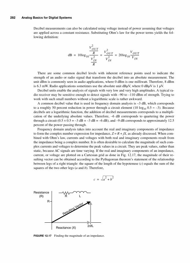
282 Analog Basics for Digital Systems
Decibel measurements can also be calculated using voltage instead of power assuming that voltagesare applied across a constant resistance. Substituting Ohm’s law for the power terms yields the fol-lowing definition:
There are some common decibel levels with inherent reference points used to indicate thestrength of an audio or radio signal that transform the decibel into an absolute measurement. Theunit dBm is commonly seen in audio applications, where 0 dBm is one milliwatt. Therefore, 8 dBmis 6.3 mW. Radio applications sometimes use the absolute unit dBµV, where 0 dBµV is 1 µV.
Decibel units enable the analysis of signals with very low and very high amplitudes. A typical ra-dio receiver may be sensitive enough to detect signals with –90 to –110 dBm of strength. Trying towork with such small numbers without a logarithmic scale is rather awkward.
A common decibel value that is used in frequency domain analysis is –3 dB, which correspondsto a roughly 50 percent reduction in power through a circuit element (10 log10 0.5 ≈ –3). Becausedecibels are a logarithmic function, the addition of decibel measurements corresponds to a multipli-cation of the underlying absolute values. Therefore, –6 dB corresponds to quartering the powerthrough a circuit (0.5 × 0.5 = –3 dB + –3 dB = –6 dB), and –9 dB corresponds to approximately 12.5percent of the power passing through.
Frequency domain analysis takes into account the real and imaginary components of impedanceto form the complex number expression for impedance, Z = R + jX, as already discussed. When com-bined with Ohm’s law, currents and voltages with both real and imaginary components result fromthe impedance being a complex number. It is often desirable to calculate the magnitude of such com-plex currents and voltages to determine the peak values in a circuit. They are peak values, rather thanstatic, because AC signals are time varying. If the real and imaginary components of an impedance,current, or voltage are plotted on a Cartesian grid as done in Fig. 12.17, the magnitude of their re-sulting vector can be obtained according to the Pythagorean theorem’s statement of the relationshipbetween legs of a right triangle: the square of the length of the hypotenuse (c) equals the sum of thesquares of the two other legs (a and b). Therefore,
dB 10log10
V OUT2
R---------------
V IN2
R----------
---------------V OUT
2
V IN2
--------------- 20log10
V OUT
V IN---------------= = =
LRResistance
(R)
Reactance (X) 2πfL
R
Resulting Vector
FIGURE 12.17 Finding the magnitude of an impedance.
c a2
b2
+=
-Balch.book Page 282 Thursday, May 15, 2003 3:46 PM

Electrical Fundamentals 283
In this example, a resistor and inductor are placed in series with a resulting impedance, Z = R +j2πfL. The magnitude is expressed as follows:
12.9 LOWPASS AND HIGHPASS FILTERS
Filtering is the general process of attenuating the energy of a certain range of frequencies whilepassing a desired range with little or no attenuation. The noise filtering examples discussed previ-ously are designated lowpass filters, because they are designed to pass lower frequencies while at-tenuating higher frequencies above a certain threshold. They are also passive filters, because thecircuits are constructed entirely of passive components (resistors, inductors, and capacitors) withoutany active components (e.g., transistors) to provide amplification. Passive filters are very practicalbecause of their simplicity and small size. They are suitable for applications wherein the signal thatis desired to pass through the filter has sufficient amplitude to be used after the filter. In situations inwhich very weak signals are involved (e.g., tuning a radio signal), amplification may be necessarybefore, after, or within the filter. Such filters are termed active filters. Whether a filter is active orpassive, the underlying analysis of how desired frequencies are passed and undesired frequencies areattenuated remains the same.
A filter’s frequency response can be determined bycombining basic circuit principles with the frequency-dependent impedance characteristics of capacitors andinductors. The most basic lowpass filter is a series resis-tor and shunt capacitor as shown in Fig. 12.18. This isreferred to as a first-order lowpass filter, because the cir-cuit contains a single AC element, a capacitor. Since acapacitor’s impedance drops as the frequency increases,higher frequencies are short-circuited to ground.
The filter’s output voltage can be calculated by combining the impedances of each element into asingle voltage-divider expression,
Rather than continuing to explicitly reference the input and output voltages, it is common to referto the filter’s transfer function, or gain (A), which is the relationship between input and output volt-age. The gain is obtained by simply dividing both sides of the equation by the input voltage.
A lowpass filter is considered to be effective starting at a certain cutoff frequency (fC), the fre-quency at which its power gain in halved. This is also called the half-power point. Recall that a deci-bel level is calculated as 10 log10 APOWER. Therefore, the filter’s gain declines by 10 log10 0.5 = –3
Z R2
2πfL( )2+=
+
–
VIN
+
–
VOUT
FIGURE 12.18 First-order RC lowpass filter.
V OUT V IN
ZC
ZC ZR+-------------------- V IN
12πfC-------------
11
2πfC------------- R+---------------------------------------------- V IN
11 2πfRC+--------------------------= = =
AFILTER
V OUT
V IN--------------- 1
1 2πfRC+--------------------------= =
-Balch.book Page 283 Thursday, May 15, 2003 3:46 PM

284 Analog Basics for Digital Systems
dB at fC. Because a passive filter has an ideal gain of zero at DC (no amplification), its gain at fC is–3 dB.
However, the gain expression for this filter is in terms of voltage, not power. The relationship be-tween voltage gain and decibel level is a multiplier of 20 rather than 10. Therefore, rather than look-ing for a gain of one-half at fC, we must find a gain equal to the square root of one half because
–3 dB =
The filter’s gain expression is complex and must be converted into a real magnitude. Conve-niently, the magnitude representation looks fairly close to what we are looking for.
By setting the denominator equal to the square root of 2, it can be observed that a gain of –3 dB isachieved when 2πf = 1 ÷ RC. Furthermore, it can be shown that the lowpass filter’s gain declines atthe rate of 20 dB per radian frequency decade because, for large f, the constant 1 in the denominatorhas an insignificant affect on the magnitude of the overall expression,
Rather than trying to keep all of these numbers in one’s head while attempting to solve a problem,it is common to plot the transfer function of a filter on a diagram called a Bode plot, named after thetwentieth century American engineer H. W. Bode. A Bode magnitude plot for this lowpass filter isshown in Fig. 12.19. Filters and AC circuits in general also modify the phase of signals that passthrough them. More complete AC analyses plot a circuit’s phase transfer function using a similarBode phase diagram. Phase diagrams are not shown, because these topics are outside the scope ofthis discussion.
20log101
2-------
AFILTER1
1 2πfRC( )2+
--------------------------------------=
20log101
2πfRC-----------------
-60
-40
-20
0
dB
Frequency (Hertz)
10X 10X+1 10X+2 10X+3
10fC
-20 dB/decade
fC=1
2πRC
FIGURE 12.19 Bode magnitude plot for RC lowpass filter.
-Balch.book Page 284 Thursday, May 15, 2003 3:46 PM
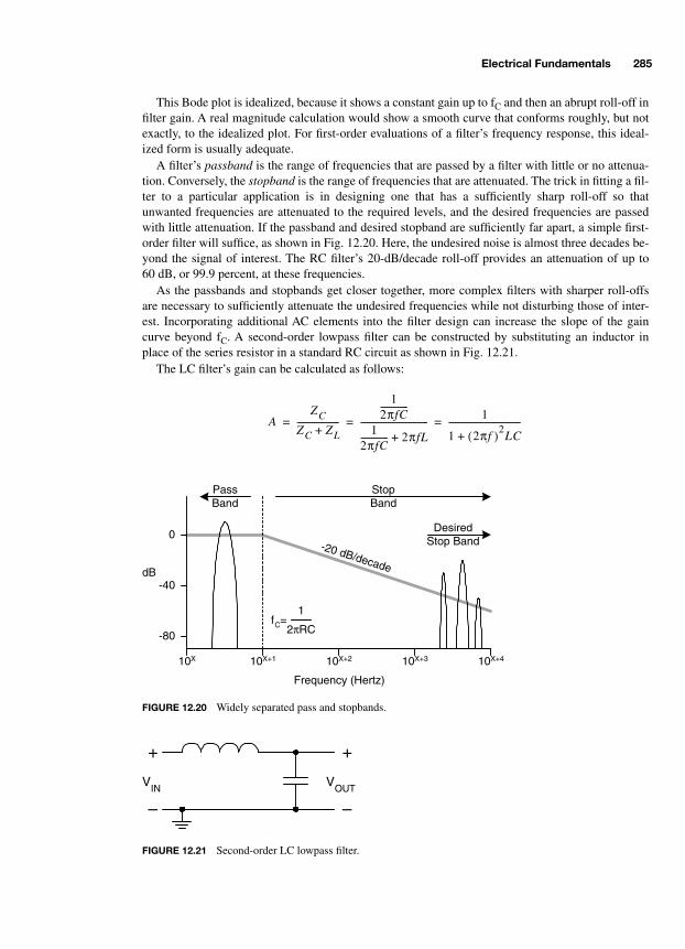
Electrical Fundamentals 285
This Bode plot is idealized, because it shows a constant gain up to fC and then an abrupt roll-off infilter gain. A real magnitude calculation would show a smooth curve that conforms roughly, but notexactly, to the idealized plot. For first-order evaluations of a filter’s frequency response, this ideal-ized form is usually adequate.
A filter’s passband is the range of frequencies that are passed by a filter with little or no attenua-tion. Conversely, the stopband is the range of frequencies that are attenuated. The trick in fitting a fil-ter to a particular application is in designing one that has a sufficiently sharp roll-off so thatunwanted frequencies are attenuated to the required levels, and the desired frequencies are passedwith little attenuation. If the passband and desired stopband are sufficiently far apart, a simple first-order filter will suffice, as shown in Fig. 12.20. Here, the undesired noise is almost three decades be-yond the signal of interest. The RC filter’s 20-dB/decade roll-off provides an attenuation of up to60 dB, or 99.9 percent, at these frequencies.
As the passbands and stopbands get closer together, more complex filters with sharper roll-offsare necessary to sufficiently attenuate the undesired frequencies while not disturbing those of inter-est. Incorporating additional AC elements into the filter design can increase the slope of the gaincurve beyond fC. A second-order lowpass filter can be constructed by substituting an inductor inplace of the series resistor in a standard RC circuit as shown in Fig. 12.21.
The LC filter’s gain can be calculated as follows:
-80
-40
0
dB
Frequency (Hertz)
10X 10X+1 10X+2 10X+3 10X+4
-20 dB/decade
PassBand
StopBand
DesiredStop Band
fC=1
2πRC
FIGURE 12.20 Widely separated pass and stopbands.
+
–
VIN
+
–
VOUT
FIGURE 12.21 Second-order LC lowpass filter.
AZC
ZC ZL+--------------------
12πfC-------------
12πfC------------- 2πfL+-------------------------------- 1
1 2πf( )2LC+
----------------------------------= = =
-Balch.book Page 285 Thursday, May 15, 2003 3:46 PM
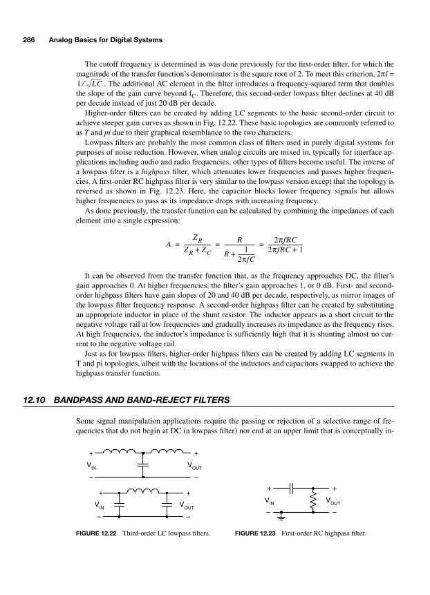
286 Analog Basics for Digital Systems
The cutoff frequency is determined as was done previously for the first-order filter, for which themagnitude of the transfer function’s denominator is the square root of 2. To meet this criterion, 2πf =
. The additional AC element in the filter introduces a frequency-squared term that doublesthe slope of the gain curve beyond fC. Therefore, this second-order lowpass filter declines at 40 dBper decade instead of just 20 dB per decade.
Higher-order filters can be created by adding LC segments to the basic second-order circuit toachieve steeper gain curves as shown in Fig. 12.22. These basic topologies are commonly referred toas T and pi due to their graphical resemblance to the two characters.
Lowpass filters are probably the most common class of filters used in purely digital systems forpurposes of noise reduction. However, when analog circuits are mixed in, typically for interface ap-plications including audio and radio frequencies, other types of filters become useful. The inverse ofa lowpass filter is a highpass filter, which attenuates lower frequencies and passes higher frequen-cies. A first-order RC highpass filter is very similar to the lowpass version except that the topology isreversed as shown in Fig. 12.23. Here, the capacitor blocks lower frequency signals but allowshigher frequencies to pass as its impedance drops with increasing frequency.
As done previously, the transfer function can be calculated by combining the impedances of eachelement into a single expression:
It can be observed from the transfer function that, as the frequency approaches DC, the filter’sgain approaches 0. At higher frequencies, the filter’s gain approaches 1, or 0 dB. First- and second-order highpass filters have gain slopes of 20 and 40 dB per decade, respectively, as mirror images ofthe lowpass filter frequency response. A second-order highpass filter can be created by substitutingan appropriate inductor in place of the shunt resistor. The inductor appears as a short circuit to thenegative voltage rail at low frequencies and gradually increases its impedance as the frequency rises.At high frequencies, the inductor’s impedance is sufficiently high that it is shunting almost no cur-rent to the negative voltage rail.
Just as for lowpass filters, higher-order highpass filters can be created by adding LC segments inT and pi topologies, albeit with the locations of the inductors and capacitors swapped to achieve thehighpass transfer function.
12.10 BANDPASS AND BAND-REJECT FILTERS
Some signal manipulation applications require the passing or rejection of a selective range of fre-quencies that do not begin at DC (a lowpass filter) nor end at an upper limit that is conceptually in-
1 LC⁄
+
–
VIN
+
–
VOUT
+
–
VIN
+
–
VOUT
+
–
VIN
+
–
VOUT
FIGURE 12.22 Third-order LC lowpass filters. FIGURE 12.23 First-order RC highpass filter.
AZR
ZR ZC+-------------------- R
R1
2πfC-------------+
----------------------- 2πfRC2πfRC 1+--------------------------= = =
-Balch.book Page 286 Thursday, May 15, 2003 3:46 PM
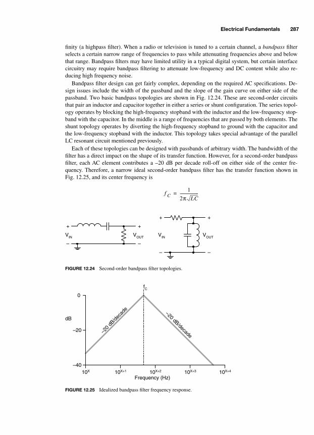
Electrical Fundamentals 287
finity (a highpass filter). When a radio or television is tuned to a certain channel, a bandpass filterselects a certain narrow range of frequencies to pass while attenuating frequencies above and belowthat range. Bandpass filters may have limited utility in a typical digital system, but certain interfacecircuitry may require bandpass filtering to attenuate low-frequency and DC content while also re-ducing high frequency noise.
Bandpass filter design can get fairly complex, depending on the required AC specifications. De-sign issues include the width of the passband and the slope of the gain curve on either side of thepassband. Two basic bandpass topologies are shown in Fig. 12.24. These are second-order circuitsthat pair an inductor and capacitor together in either a series or shunt configuration. The series topol-ogy operates by blocking the high-frequency stopband with the inductor and the low-frequency stop-band with the capacitor. In the middle is a range of frequencies that are passed by both elements. Theshunt topology operates by diverting the high-frequency stopband to ground with the capacitor andthe low-frequency stopband with the inductor. This topology takes special advantage of the parallelLC resonant circuit mentioned previously.
Each of these topologies can be designed with passbands of arbitrary width. The bandwidth of thefilter has a direct impact on the shape of its transfer function. However, for a second-order bandpassfilter, each AC element contributes a –20 dB per decade roll-off on either side of the center fre-quency. Therefore, a narrow ideal second-order bandpass filter has the transfer function shown inFig. 12.25, and its center frequency is
+
–
VIN
+
–
VOUT
+
–
VIN
+
–
VOUT
FIGURE 12.24 Second-order bandpass filter topologies.
–40
–20
0
dB
Frequency (Hz)10X 10X+1 10X+2 10X+3
fC
–20 dB/decade
10X+4
–20
dB/d
ecad
e
FIGURE 12.25 Idealized bandpass filter frequency response.
f C1
2π LC-------------------=
-Balch.book Page 287 Thursday, May 15, 2003 3:46 PM

288 Analog Basics for Digital Systems
By now, the symmetry of filtering leaves no surprise that a bandpass topology can be rearrangedto form a band-reject filter, often called a notch filter. Whereas the bandpass filter passes a narrowrange of frequencies, a band-reject filter attenuates a narrow range of frequencies. The two basic sec-ond-order band-reject filter topologies are shown in Fig. 12.26. In the reverse of a bandpass filter, theseries topology takes advantage of the LC circuit’s high impedance at its resonant frequency to blockthe incoming signal. Similarly, the shunt topology’s low combined impedance at a narrow range offrequencies diverts that energy to ground.
Digital systems often require only that a filter attenuate unwanted frequencies, typically noise, tothe point at which the digital circuitry is not adversely impacted by that noise. Clock generators andclock circuits are usually the digital components that are most sensitive to noise. Alternatively, digi-tal systems that incorporate sensitive analog interface components may require filters to separate and“clean up” the power, data, and control signals that pass between the digital and analog circuitry.Such applications often require only a first-order of approximation to determine cutoff or center fre-quencies for filters.
Designing filters for analog applications where specific characteristics of transfer functionshave a major impact on circuit performance requires far more detailing and circuit analysis theorythan has been presented here. If your filter is more analog than digital in its application, you arestrongly advised to spend time in obtaining a thorough understanding of AC circuit analysis andfilter design.
12.11 TRANSFORMERS
When two inductors are placed together in close proximity, they exhibit mutual inductance whereone coil’s magnetic field couples onto the other coil and vice-versa. This behavior may be undesiredin many situations and can be largely avoided by physically separating individual inductors. How-ever, the phenomenon of mutual inductance has great benefit when two or more coils are assembledtogether to form a transformer. Mutual inductance is enhanced not only by close physical proximity,but also by winding the transformer’s coils around common cores made from ferrous metals thatconduct magnetic fields. Transformers have many uses, but their basic function is to transfer AC en-ergy from one coil to another without having a DC connection between the two ends. A transformerdoes not pass DC because there is no direct connection between the two coils.
Neglecting losses resulting from finite resistance and less-than-ideal efficiency in magnetic fieldcoupling, the voltage excited in one coil winding is related to that created in another winding by theproportion of the number of winding turns (N) in each coil. A transformer with two windings is saidto have a primary and a secondary winding. The voltage relationship of each winding in an idealtransformer is as follows:
+
–
+
–
VOUT
+
–
VIN
+
–
VOUT
FIGURE 12.26 Second-order band-reject filter topologies.
-Balch.book Page 288 Thursday, May 15, 2003 3:46 PM

Electrical Fundamentals 289
A transformer is a passive component; it has no capability of amplifying a signal. Consequently, anideal transformer passes 100 percent of the power applied to it and satisfies the equation VSIS = VPIP.If the primary coil has more windings than the secondary coil, an AC signal of lesser magnitude willbe induced on the secondary coil when an AC signal is applied to the primary coil. The current flow-ing through the secondary coil will be higher than that in the primary so that conservation of energy ispreserved. In reality, of course, a transformer has less than 100 percent efficiency as a result of para-sitic properties, including finite resistance of the coils and less-than-perfect magnetic coupling.
One of the most common uses of a transformer is in power distribution in which AC power is ei-ther stepped up or stepped down, depending on the application. Figure 12.27 shows a basic trans-former with a 120 VAC signal injected into the primary coil and a load resistor on the secondary coil.The ratio of the primary to secondary windings is 10:1; perhaps the primary coil has 1,000 windingswhereas the secondary has 100. The result is a step-down of high-voltage power from a wall outlet toa more manageable 12 VAC. This illustrates why AC power distribution is so convenient: voltagescan be arbitrarily transformed without any complicated electronic circuits. It is advantageous to dis-tribute power at a higher voltage to reduce the current draw for a given power level. Lower currentmeans lower I2R power losses in the distribution wiring. The 12 VAC transformer output may powerthe voltage regulator of a digital circuit. If the digital circuit draws 10 A at 12 VAC, it will draw only1 A at 120 VAC.
Transformers are critical to power distribution both at the system level and at the generation andutility levels. Power is stepped up at generating plants with transformers to as high as 765,000 V forefficient long-distance distribution. As the power gets closer to your home or office, it is steppeddown to intermediate levels and finally enters the premises at 120 and 240 VAC.
Aside from power supply applications, transformers are also used for filtering and impedancematching of interface signals. The use of a transformer as a filter requires knowledge of the physicalorientations of the primary and secondary windings with respect to one another. Each winding in atransformer has two terminals. When a signal is applied to the primary coil, a decision is made as towhich terminal is connected to the positive portion of the circuit and which is connected to the nega-tive portion (ground in some applications). That signal will induce a signal of equivalent polarity onthe secondary coil when the appropriate choice of positive and negative terminals is made at theother end of the transformer. Alternatively, a signal of opposite polarity will be induced if the sec-ondary coil’s positive and negative connections are swapped. The graphical convention of distin-guishing the matching terminals of the primary and secondary coils is by placing matching referencedots next to one terminal of each coil as shown in Fig. 12.28. The coils may be drawn with their dotson the same side or on opposite ends of the transformer.
The relative polarity of the primary and secondary windings is important for filtering applicationsto ensure that magnetic fields in each coil either add to or cancel each other as appropriate. Trans-
V PRIMARY
V SECONDARY------------------------------------
NPRIMARY
NSECONDARY------------------------------------=
10:1
RLOAD120 VAC
Input
12 VAC Output
FIGURE 12.27 Basic transformer operation.
-Balch.book Page 289 Thursday, May 15, 2003 3:46 PM
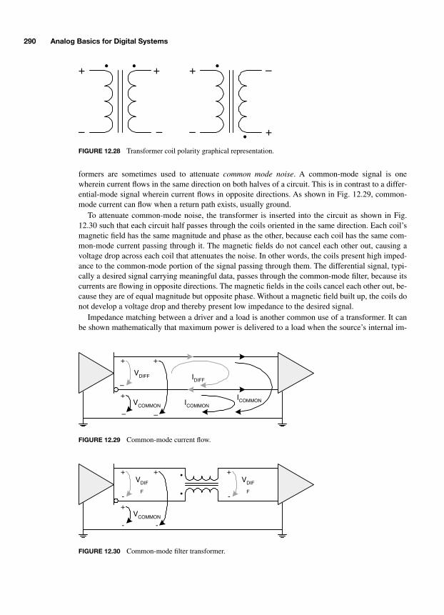
290 Analog Basics for Digital Systems
formers are sometimes used to attenuate common mode noise. A common-mode signal is onewherein current flows in the same direction on both halves of a circuit. This is in contrast to a differ-ential-mode signal wherein current flows in opposite directions. As shown in Fig. 12.29, common-mode current can flow when a return path exists, usually ground.
To attenuate common-mode noise, the transformer is inserted into the circuit as shown in Fig.12.30 such that each circuit half passes through the coils oriented in the same direction. Each coil’smagnetic field has the same magnitude and phase as the other, because each coil has the same com-mon-mode current passing through it. The magnetic fields do not cancel each other out, causing avoltage drop across each coil that attenuates the noise. In other words, the coils present high imped-ance to the common-mode portion of the signal passing through them. The differential signal, typi-cally a desired signal carrying meaningful data, passes through the common-mode filter, because itscurrents are flowing in opposite directions. The magnetic fields in the coils cancel each other out, be-cause they are of equal magnitude but opposite phase. Without a magnetic field built up, the coils donot develop a voltage drop and thereby present low impedance to the desired signal.
Impedance matching between a driver and a load is another common use of a transformer. It canbe shown mathematically that maximum power is delivered to a load when the source’s internal im-
+
–
+
–
+
– +
–
FIGURE 12.28 Transformer coil polarity graphical representation.
IDIFF
ICOMMON
VDIFF
+
–
+
+
–
VCOMMON
–
ICOMMON
FIGURE 12.29 Common-mode current flow.
VDIF
F
+
-
+
+
-
VCOMMON
-
VDIF
F
+
-
FIGURE 12.30 Common-mode filter transformer.
-Balch.book Page 290 Thursday, May 15, 2003 3:46 PM

Electrical Fundamentals 291
pedance equals that of the load. Under these conditions, only half of the total power is delivered tothe load, the remaining half being dissipated by the source impedance. For unequal load and sourceimpedances, more or less voltage and current will be delivered to the load, but always in proportionsthat result in less than 50 percent of the total power. It may be desirable to deliver maximum power toa load in situations where the impedance of a driver (e.g., audio amplifier) does not match that of itsload (e.g., speaker). A transformer can be used to isolate the source and load from each other andpresent each with the necessary impedance for maximum power transfer.
If a load resistor is connected to a transformer’s secondary coil as shown in Fig. 12.31, Ohm’s lawcan be used to relate VP and IP by RLOAD. To simplify the analysis, the secondary coil is said to haveone winding and the primary N windings, for a simple N:1 ratio. Therefore,
More primary windings increase the voltage ratio between the primary and secondary but de-crease the current because a transformer cannot amplify a signal and, hence, VPIP = –VSIS. The cur-rent in the secondary winding flows in the direction opposite of that in the primary, because theprimary is feeding current into the transformer and the load is pulling current out.
It is known that the relationship between the voltages on either side of the transformer is given byVP = NVS and that, maintaining proper current polarity, VS = –ISRLOAD. Therefore, VP = –NISRLOAD.The secondary current term can be substituted out of the equation by using the relationship of cur-rents to coil windings, IS = –NIP, to yield VP = N2IPRLOAD. Finally, Ohm’s law is used to remove theprimary voltage and current terms: RSOURCE = N2RLOAD. Put in more general terms, RP = N2RS.
A high ratio of primary to secondary windings will present the signal source with an apparentlyhigher impedance than is actually connected to the secondary. Similarly, the load will be presentedwith an apparently lower impedance than is actually present in the source. Considering the circuit inFig. 12.32, an 8-Ω speaker can be matched to an amplifier with a 100-Ω output impedance using atransformer with a 3.5:1 winding ratio.
RLOAD
RSOURCE
N:1
IP
Source
IS
VS
+
–
VP
+
–
FIGURE 12.31 Impedance transformation.
V P
V S------- N
1----= and
IP
IS----- 1
N----–=
8 Ω100 Ω
3.5:1
Source
FIGURE 12.32 Amplifier/speaker impedance matching.
-Balch.book Page 291 Thursday, May 15, 2003 3:46 PM

This page intentionally left blank.
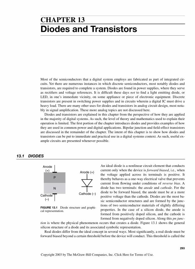
293
CHAPTER 13
Diodes and Transistors
Most of the semiconductors that a digital system employs are fabricated as part of integrated cir-cuits. Yet there are numerous instances in which discrete semiconductors, most notably diodes andtransistors, are required to complete a system. Diodes are found in power supplies, where they serveas rectifiers and voltage references. It is difficult these days
not
to find a light emitting diode, orLED, in one’s immediate vicinity, on some appliance or piece of electronic equipment. Discretetransistors are present in switching power supplies and in circuits wherein a digital IC must drive aheavy load. There are many other uses for diodes and transistors in analog circuit design, most nota-bly in signal amplification. These more analog topics are not discussed here.
Diodes and transistors are explained in this chapter from the perspective of how they are appliedin the majority of digital systems. As such, the level of theory and mathematics used to explain theiroperation is limited. The first portion of the chapter introduces diodes and provides examples of howthey are used in common power and digital applications. Bipolar junction and field-effect transistorsare discussed in the remainder of the chapter. The intent of this chapter is to show how diodes andtransistors can be put to immediate and practical use in a digital systems context. As such, useful ex-ample circuits are presented whenever possible.
13.1 DIODES
An ideal diode is a nonlinear circuit element that conductscurrent only when the device is
forward biased
, i.e., whenthe voltage applied across its terminals is positive. Itthereby behaves as a one-way electrical valve that preventscurrent from flowing under conditions of
reverse bias
. Adiode has two terminals: the
anode
and
cathode
. For thediode to be forward biased, the anode must be at a morepositive voltage than the cathode. Diodes are the most ba-sic semiconductor structures and are formed by the junc-tions of two semiconductor materials of slightly differingproperties. In the case of a silicon diode, the anode isformed from positively doped silicon, and the cathode isformed from negatively doped silicon. Along this
pn junc-tion
is where the physical phenomenon occurs that creates a diode. Figure 13.1 shows the generalsilicon structure of a diode and its associated symbolic representation.
Real diodes differ from the ideal concept in several ways. Most significantly, a real diode must beforward biased beyond a certain threshold before the device will conduct. This threshold is called the
N
P
Cathode(–)
Anode(+) Anode (+)
Cathode (–)
FIGURE 13.1 Diode structure and graphi-cal representation.
-Balch.book Page 293 Thursday, May 15, 2003 3:46 PM
Copyright 2003 by The McGraw-Hill Companies, Inc. Click Here for Terms of Use.

294 Analog Basics for Digital Systems
forward voltage
,
V
F
. A diode conducts very little current below
V
F
, measured in micro- or nano-amps. The relationship between a diode’s current and voltage is exponential and therefore increasesrapidly around
V
F
. Above
V
F
, the diode presents very low impedance and appears almost like a shortcircuit, or a piece of wire. A typical silicon diode’s I-V characteristic is shown in Fig. 13.2 with
V
F
ofapproximately 0.7 V. For many applications, especially those in digital systems, a diode’s I-V char-acteristic can be simplified to a step function from zero to infinite current at the forward voltage.Real diodes also have a reverse breakdown voltage, called the
Zener
voltage,
V
Z
, at which point theywill conduct under reverse-biased conditions. Normal diodes are usually not subjected to reverse-bias voltages sufficient to achieve significant conduction. Special-purpose Zener diodes are designedspecifically to operate under reverse-bias conditions and are commonly used in voltage referenceand regulation applications.
Saying that a diode conducts “infinite” current beyond
V
F
really means that its impedance be-comes so low that it no longer becomes the limiting factor in a circuit. If a typical diode is connecteddirectly to a battery such that it is forward biased, the diode will form nearly a short circuit, whichwill cause a large current flow. Fairly soon afterward, the diode will likely fail due to thermal over-load. Diodes are specified with maximum
forward currents
,
I
F
. Exceeding
I
F
causes the diode to dis-sipate more power than it is designed for, usually with destructive consequences.
When a diode is used in an application wherein it may be forward biased and driven with exces-sive current, a current-limiting resistor is inserted into the circuit to keep the diode within its speci-fied operating limits. Diodes are useful for providing a fixed voltage reference regardless of acircuit’s operating voltage. The circuit shown in Fig. 13.3 takes advantage of a diode’s relativelystatic forward voltage with respect to current. A loosely regulated 12-V supply may have a toleranceof ±20 percent—a range of 9.6 to 14.4 V. If a resistor divider is used to generate a reference voltage,its accuracy could be no better than that of the 12-V supply. Some applications require a more accu-rate voltage reference with which to sense an incoming signal. A 1N4148 exhibits
V
F
= 0.7 V at
VF
I
VZ
Compressed Negative Voltage Scale:|VZ|>>VF
FIGURE 13.2 Silicon diode I-V characteristic.
-Balch.book Page 294 Thursday, May 15, 2003 3:46 PM
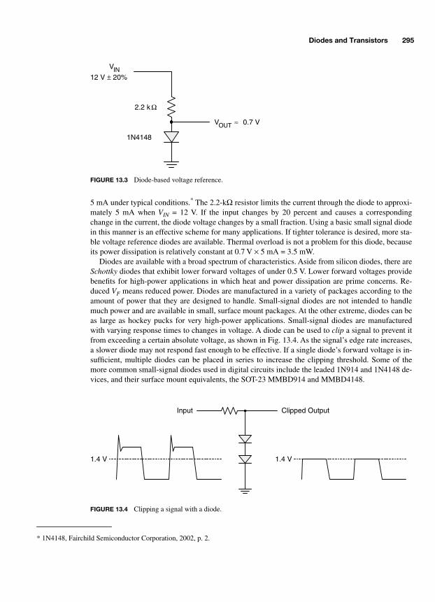
Diodes and Transistors 295
5 mA under typical conditions.
*
The 2.2-k
Ω
resistor limits the current through the diode to approxi-mately 5 mA when
V
IN
= 12 V. If the input changes by 20 percent and causes a correspondingchange in the current, the diode voltage changes by a small fraction. Using a basic small signal diodein this manner is an effective scheme for many applications. If tighter tolerance is desired, more sta-ble voltage reference diodes are available. Thermal overload is not a problem for this diode, becauseits power dissipation is relatively constant at 0.7 V
×
5 mA = 3.5 mW.Diodes are available with a broad spectrum of characteristics. Aside from silicon diodes, there are
Schottky
diodes that exhibit lower forward voltages of under 0.5 V. Lower forward voltages providebenefits for high-power applications in which heat and power dissipation are prime concerns. Re-duced
V
F
means reduced power. Diodes are manufactured in a variety of packages according to theamount of power that they are designed to handle. Small-signal diodes are not intended to handlemuch power and are available in small, surface mount packages. At the other extreme, diodes can beas large as hockey pucks for very high-power applications. Small-signal diodes are manufacturedwith varying response times to changes in voltage. A diode can be used to
clip
a signal to prevent itfrom exceeding a certain absolute voltage, as shown in Fig. 13.4. As the signal’s edge rate increases,a slower diode may not respond fast enough to be effective. If a single diode’s forward voltage is in-sufficient, multiple diodes can be placed in series to increase the clipping threshold. Some of themore common small-signal diodes used in digital circuits include the leaded 1N914 and 1N4148 de-vices, and their surface mount equivalents, the SOT-23 MMBD914 and MMBD4148.
* 1N4148, Fairchild Semiconductor Corporation, 2002, p. 2.
2.2 k Ω
VIN12 V ± 20%
VOUT ≈ 0.7 V
1N4148
FIGURE 13.3 Diode-based voltage reference.
Input Clipped Output
1.4 V 1.4 V
FIGURE 13.4 Clipping a signal with a diode.
-Balch.book Page 295 Thursday, May 15, 2003 3:46 PM

296 Analog Basics for Digital Systems
13.2 POWER CIRCUITS WITH DIODES
A major use for diodes is in the
rectification
of AC signals, specifically in power supplies in whichthe conversion from AC to DC is required. Small-signal diodes can be used as rectifiers in non-power or low-power applications. Larger diodes with higher power ratings are employed when con-structing power supply circuits meant to provide more power. An AC power signal is a sine wave ofarbitrary amplitude that is centered about 0 V. Its voltage peaks are of equal magnitude above andbelow 0 V. A digital circuit requires a steady DC power supply. The first step in creating a steady DCpower supply is to rectify the AC input such that the negative AC sine wave excursions are blocked.Figure 13.5 shows a single diode performing this function. The rectified output is reduced in voltageby the diode’s forward voltage. This circuit is called a
half-wave
rectifier, because it passes only halfof the incoming power signal. Once rectified, capacitors and inductors can smooth out (lowpass fil-ter) the rectified AC signal to create a steady DC output.
The single-diode half-wave rectifier does the job, but does not take advantage of the negativeportion of the AC input. Four diodes can be assembled into a
full-wave bridge rectifier
that passesthe positive portion of the sine wave and inverts the negative portion relative to the DC ground. Thiscircuit is shown in Fig. 13.6. The bridge rectifier works by providing a current conduction paththrough the resistor to ground regardless of the polarity of the incoming AC signal. When the AC in-put is positive with respect to the polarity markings shown in the diagram, diodes D1 and D3 areforward biased, conducting current from D1 through the resistor, then through D3 to the negativeAC input wire. When the AC input is negative during the next half of the sinusoid, D2 and D4 areforward biased and allow current to flow in the same direction through the resistor. The result is thata positive voltage is always developed across the load with respect to ground. Note that, because ofthe two diodes in series with the load, the rectified output voltage is reduced by twice the diodes’forward voltage.
Power rectifier circuits are generally found in systems wherein a high-voltage input (e.g.,120 VAC) must be converted into a low-voltage output such as +5 VDC to power a digital logic cir-cuit. Transformers are used in conjunction with bridge rectifiers to step down the high-voltage ACinput to a more appropriate intermediate level that is much closer to the final voltage level requiredby the system. A power filter circuit can then be used to smooth the heavily rippled rectified signalinto a more stable DC input. Finally, a voltage regulator performs the final adjustments to convert the
Rectified Output
RLOADAC Input
0 V
+VMAX
–VMAX
0 V
+VMAX
VF loss
FIGURE 13.5 Half-wave rectifier circuit.
-Balch.book Page 296 Thursday, May 15, 2003 3:46 PM
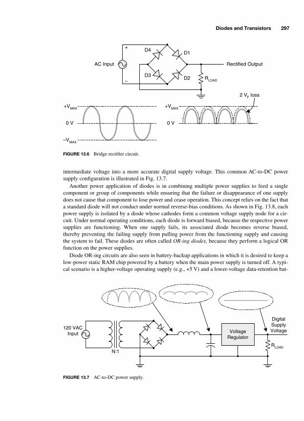
Diodes and Transistors 297
intermediate voltage into a more accurate digital supply voltage. This common AC-to-DC powersupply configuration is illustrated in Fig. 13.7.
Another power application of diodes is in combining multiple power supplies to feed a singlecomponent or group of components while ensuring that the failure or disappearance of one supplydoes not cause that component to lose power and cease operation. This concept relies on the fact thata standard diode will not conduct under normal reverse-bias conditions. As shown in Fig. 13.8, eachpower supply is isolated by a diode whose cathodes form a common voltage supply node for a cir-cuit. Under normal operating conditions, each diode is forward biased, because the respective powersupplies are functioning. When one supply fails, its associated diode becomes reverse biased,thereby preventing the failing supply from pulling power from the functioning supply and causingthe system to fail. These diodes are often called
OR-ing diodes,
because they perform a logical ORfunction on the power supplies.
Diode OR-ing circuits are also seen in battery-backup applications in which it is desired to keep alow-power static RAM chip powered by a battery when the main power supply is turned off. A typi-cal scenario is a higher-voltage operating supply (e.g., +5 V) and a lower-voltage data-retention bat-
Rectified Output
RLOAD
AC Input
0 V
+VMAX
–VMAX
0 V
+VMAX
+
–
D1
D2
D4
D3
2 VF loss
FIGURE 13.6 Bridge rectifier circuit.
N:1
DigitalSupplyVoltage
RLOAD
120 VACInput Voltage
Regulator
FIGURE 13.7 AC-to-DC power supply.
-Balch.book Page 297 Thursday, May 15, 2003 3:46 PM
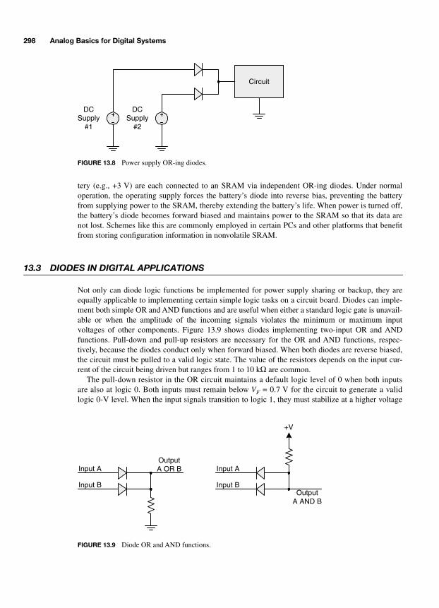
298 Analog Basics for Digital Systems
tery (e.g., +3 V) are each connected to an SRAM via independent OR-ing diodes. Under normaloperation, the operating supply forces the battery’s diode into reverse bias, preventing the batteryfrom supplying power to the SRAM, thereby extending the battery’s life. When power is turned off,the battery’s diode becomes forward biased and maintains power to the SRAM so that its data arenot lost. Schemes like this are commonly employed in certain PCs and other platforms that benefitfrom storing configuration information in nonvolatile SRAM.
13.3 DIODES IN DIGITAL APPLICATIONS
Not only can diode logic functions be implemented for power supply sharing or backup, they areequally applicable to implementing certain simple logic tasks on a circuit board. Diodes can imple-ment both simple OR and AND functions and are useful when either a standard logic gate is unavail-able or when the amplitude of the incoming signals violates the minimum or maximum inputvoltages of other components. Figure 13.9 shows diodes implementing two-input OR and ANDfunctions. Pull-down and pull-up resistors are necessary for the OR and AND functions, respec-tively, because the diodes conduct only when forward biased. When both diodes are reverse biased,the circuit must be pulled to a valid logic state. The value of the resistors depends on the input cur-rent of the circuit being driven but ranges from 1 to 10 k
Ω
are common.The pull-down resistor in the OR circuit maintains a default logic level of 0 when both inputs
are also at logic 0. Both inputs must remain below
V
F
= 0.7 V for the circuit to generate a validlogic 0-V level. When the input signals transition to logic 1, they must stabilize at a higher voltage
Circuit
DCSupply
#2
DCSupply
#1
FIGURE 13.8 Power supply OR-ing diodes.
Input A
Input B
OutputA OR B Input A
Input BOutput
A AND B
+V
FIGURE 13.9 Diode OR and AND functions.
-Balch.book Page 298 Thursday, May 15, 2003 3:46 PM
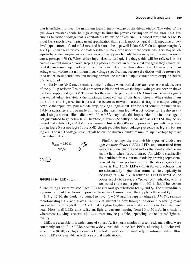
Diodes and Transistors 299
that is sufficient to meet the minimum logic-1 input voltage of the driven circuit. The value of thepull-down resistor should be high enough to limit the power consumption of the circuit but lowenough to create a voltage that is comfortably below the driven circuit’s logic-0 threshold. A CMOSinput has a much lower input current specification than a TTL input. A typical TTL input has a low-level input current of under 0.5 mA, and it should be kept well below 0.8 V for adequate margin. A1-k
Ω
pull-down resistor would create less than a 0.5-V drop under these conditions. This may be ad-equate for some designs, or a more conservative approach could be taken by using a smaller resis-tance, perhaps 470
Ω
. When either input rises to its logic-1 voltage, this will be reflected in thecircuit’s output minus a diode drop. This places a restriction on the input voltages: they cannot ex-ceed the maximum input voltage of the driven circuit by more than a diode drop. However, the inputvoltages can violate the minimum input voltage specification, because the diodes will be reverse bi-ased under these conditions and thereby prevent the circuit’s output voltage from dropping below0 V, or ground.
Similarly, the AND circuit emits a logic-1 voltage when both diodes are reverse biased, becauseof the pull-up resistor. The diodes are reverse biased whenever the input voltages are near or abovethe logic supply voltage, +V. This enables the circuit to perform the AND function for input signalsthat would otherwise violate the maximum input voltage of the driven circuit. When either inputtransitions to a logic 0, that input’s diode becomes forward biased and drags the output voltagedown to the input level plus a diode drop, driving a logic-0 out. For the AND circuit to function re-liably, a guarantee must be made of meeting the maximum logic-0 input voltage for the driven cir-cuit. Using a normal silicon diode with
V
F
= 0.7 V may make this impossible if the input voltage isnot guaranteed to go below 0 V. Therefore, a low-
V
F
Schottky diode such as a BAT54 may be re-quired that exhibits
V
F
< 0.4 V at low currents. Just as the OR-circuit provides input voltage protec-tion at logic 0 but not logic 1, the AND-circuit provides input voltage protection at logic 1 but notlogic 0. The input voltage must not fall below the driven circuit’s minimum input voltage by morethan a diode drop.
Finally, perhaps the most visible types of diodes are
light emitting diodes
(LEDs). LEDs are constructed fromvarious semiconductors and metals that emit visible or in-visible light when forward biased. An LED is graphicallydistinguished from a normal diode by drawing representa-tions of light or photons next to the diode symbol asshown in Fig. 13.10. LEDs exhibit forward voltages thatare substantially higher than normal diodes, typically inthe range of 2 to 3 V. Whether an LED is wired to thepower supply to provide a “power on” indicator, or it isconnected to the output pin of an IC, it should be
currentlimited
using a series resistor. Each LED has its own specifications for
V
F
and
I
F
. The current-limit-ing resistor should be chosen to provide the required current given the supply voltage and
V
F
.In Fig. 13.10, the diode is assumed to have
V
F
= 2 V, and the supply voltage is 5 V. The resistortherefore drops 3 V and allows 13.6 mA of current to flow through the circuit. Allowing morecurrent to flow through the LED will make it glow brighter but will also cause it to dissipate moreheat. Most small LEDs emit sufficient light at currents ranging from 10 to 30 mA. In situationswhere power savings are critical, less current may be possible, depending on the desired light in-tensity.
LEDs are available in a wide range of colors. At first, only shades of green, red, and yellow werecommonly found. Blue LEDs became widely available in the late 1990s, allowing full-color red-green-blue (RGB) displays. Common household remote control units rely on infrared LEDs. Ultra-violet LEDs are available as well for special applications.
5 V
RLIMIT = 220 Ω
FIGURE 13.10 LED circuit.
-Balch.book Page 299 Thursday, May 15, 2003 3:46 PM

300 Analog Basics for Digital Systems
13.4 BIPOLAR JUNCTION TRANSISTORS
Transistors are silicon switches that enable a weak signal to control a much larger current flow,which is the process of amplification: magnifying the amplitude of a signal.
Bipolar junction transis-tors
(BJTs) are a basic type of transistor and are formed by two back-to-back pn junctions. Figure13.11 shows the general BJT structures and their associated symbolic representations. The BJT con-sists of three layers, or regions, of silicon in either of two configurations: NPN and PNP. The middleregion is called the
base
, and the two outer regions are separately referred to as the
collector
and
emitter
. As will soon be shown, the base-emitter junction is what enables control of a potentiallylarge current flow between the collector and emitter with a very small base-emitter current. A BJT’sconstruction is more than simply placing two diodes back to back. The base region is extremely thinto enable conduction between the collector and emitter, and the collector and emitter are sized differ-ently according to the fabrication process.
Currents in an NPN transistor flow from the base to the emitter and from the collector to the emit-ter. The relationship between these currents is defined by a proportionality constant called beta (
β
,also known as h
FE
):
I
C
=
β
I
B
. Beta is specific to each type of transistor and is characterized by themanufacturer in data sheets. Typical values for beta are from 100 to less than 1000. The beta currentrelationship provides a quick view of how a small base current can control a much larger collectorcurrent. A higher beta indicates greater potential for signal amplification. Because the base-emitterjunction is essentially a diode, it must be sufficiently forward biased for the transistor to conduct cur-rent (
V
BE
= 0.7 V under typical conditions). A PNP transistor functions similarly, although the polar-ities of currents and voltages are reversed.
When a transistor circuit is designed, care must be taken not to overdrive the base-emitter junc-tion. Like any other diode, it presents very low impedance beyond its forward voltage. Without sometype of current limiting, the transistor will overheat and become damaged. Transistors are biased us-ing resistors placed at two or three of its terminals to establish suitable operating voltages. Figure13.12 shows a common NPN configuration at DC with a current limiting resistor,
R
B
, at the base anda voltage-dropping resistor,
R
C
, at the collector. The emitter is grounded, establishing the base volt-age,
V
B
, at 0.7 V.
R
B
sets the current flowing into the base and thereby controls the collector voltage,
V
C
. As
R
B
increases,
V
C
increases, because less current is pulled through the collector, reducing thevoltage drop across
R
C
. In this example, the base current,
I
B
, is (5 V –
V
B
) +
R
B
= 0.43 mA. Assum-ing a beta of 100, the collector current,
I
C
, is 43 mA, and
V
C
= 5 V –
I
C
R
C
= 2.85 V.The transistor is limited in how much current it can drive by both its physical characteristics and
the manner in which it is biased. Physically speaking, a transistor will have a specified maximumpower dissipation beyond which it will overheat and eventually become damaged. In this circuit, thetransistor’s power dissipation is
V
C
E
I
C
+
V
B
E
I
B
, although the dominant term is between the collectorand emitter, where the great majority of the current flow exists. Using this small simplification, thetransistor is dissipating approximately 2.85 V
×
43 mA = 123 mW.
N
P
Emitter
Base
Collector
Emitter
Base
Emitter
Collector
N
BaseCollector
P
N
Emitter
P
BaseCollector
FIGURE 13.11 NPN and PNP BJT structures and graphical representations.
-Balch.book Page 300 Thursday, May 15, 2003 3:46 PM

Diodes and Transistors 301
Assuming that a transistor is not operated beyond its physical limitations, the bias configurationplaces an upper limit on how much current flows into the collector. A BJT has three modes of opera-tion: cutoff, active, and saturation. In cutoff, the transistor is not conducting, because the base-emit-ter junction is either reverse biased or insufficiently forward biased. The collector is at its maximumvoltage, and the base-collector junction is reverse biased, because no current is flowing to create avoltage drop through RC or its equivalent. When the base-emitter junction is forward biased, thetransistor conducts current and VC begins to drop. The transistor is in active mode. As long as thebase-collector junction remains reverse biased, increasing base current will cause a correspondingincrease in collector current, and the transistor remains in active mode. If IB is increased to the pointat which the base-collector junction is forward biased (increased IC causes VC to approach VE), thetransistor enters saturation and no longer can draw more current through the collector. Saturationdoes not damage the transistor, but it results in a nonlinear relationship between IB and IC , nullifyingthe effect of beta. If RC is increased or decreased, saturation occurs at lower or higher IC, respec-tively. Amplifier circuits must avoid saturation to function properly because of the resulting nonlin-earity. When used in a purely digital context, however, transistors can be driven from cutoff tosaturation as long as the power dissipation specifications are obeyed.
13.5 DIGITAL AMPLIFICATION WITH THE BJT
With a basic knowledge of BJT operation, an NPN transistor can be already be applied in a usefuldigital application: driving a high-current LED array with a relatively weak output pin from a logicIC. Typical digital output pins have relatively low current drive capabilities, because they are de-signed primarily to interface with other logic gates that have low input current requirements. CMOSlogic ICs tend to exhibit symmetrical drive currents in both logic 1 and logic 0. A CMOS output maybe rated for anywhere from several milliamps to tens of milliamps. Bipolar logic ICs tend to exhibitrelatively low drive current at logic 1, often less than one milliamp, and higher currents of severalmilliamps at logic 0. The use of bipolar logic is widespread, and it is often advantageous to take ad-vantage of the greater drive capability of the logic-0 state. Figure 13.13 shows a logic output con-nected directly to an LED with each of the two possible polarities. The active-low configurationturns the LED on when the output is logic 0, and the active-high turns the LED on when the output islogic 1.
If neither the logic-1 nor logic-0 current capabilities are sufficient for the load, a simple transistorcircuit can solve the problem. A typical 74LS logic family output pin is specified to source 0.4 mA at2.7 V when driving a logic 1. Assuming a minimum beta of 100, an NPN transistor can be used to
RB
10 k Ω
+5 VRC
+5 V
50 Ω
VE = 0 V
FIGURE 13.12 NPN DC topology.
-Balch.book Page 301 Thursday, May 15, 2003 3:46 PM
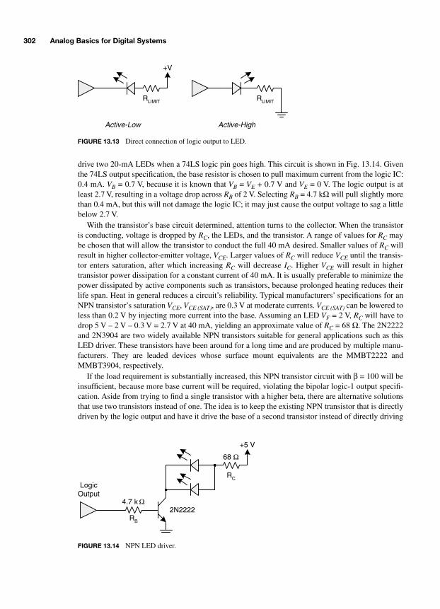
302 Analog Basics for Digital Systems
drive two 20-mA LEDs when a 74LS logic pin goes high. This circuit is shown in Fig. 13.14. Giventhe 74LS output specification, the base resistor is chosen to pull maximum current from the logic IC:0.4 mA. VB = 0.7 V, because it is known that VB = VE + 0.7 V and VE = 0 V. The logic output is atleast 2.7 V, resulting in a voltage drop across RB of 2 V. Selecting RB = 4.7 kΩ will pull slightly morethan 0.4 mA, but this will not damage the logic IC; it may just cause the output voltage to sag a littlebelow 2.7 V.
With the transistor’s base circuit determined, attention turns to the collector. When the transistoris conducting, voltage is dropped by RC, the LEDs, and the transistor. A range of values for RC maybe chosen that will allow the transistor to conduct the full 40 mA desired. Smaller values of RC willresult in higher collector-emitter voltage, VCE. Larger values of RC will reduce VCE until the transis-tor enters saturation, after which increasing RC will decrease IC. Higher VCE will result in highertransistor power dissipation for a constant current of 40 mA. It is usually preferable to minimize thepower dissipated by active components such as transistors, because prolonged heating reduces theirlife span. Heat in general reduces a circuit’s reliability. Typical manufacturers’ specifications for anNPN transistor’s saturation VCE, VCE (SAT), are 0.3 V at moderate currents. VCE (SAT) can be lowered toless than 0.2 V by injecting more current into the base. Assuming an LED VF = 2 V, RC will have todrop 5 V – 2 V – 0.3 V = 2.7 V at 40 mA, yielding an approximate value of RC = 68 Ω. The 2N2222and 2N3904 are two widely available NPN transistors suitable for general applications such as thisLED driver. These transistors have been around for a long time and are produced by multiple manu-facturers. They are leaded devices whose surface mount equivalents are the MMBT2222 andMMBT3904, respectively.
If the load requirement is substantially increased, this NPN transistor circuit with β = 100 will beinsufficient, because more base current will be required, violating the bipolar logic-1 output specifi-cation. Aside from trying to find a single transistor with a higher beta, there are alternative solutionsthat use two transistors instead of one. The idea is to keep the existing NPN transistor that is directlydriven by the logic output and have it drive the base of a second transistor instead of directly driving
+V
RLIMIT
Active-Low
RLIMIT
Active-High
FIGURE 13.13 Direct connection of logic output to LED.
+5 V
RC
LogicOutput
RB
4.7 k Ω
68 Ω
2N2222
FIGURE 13.14 NPN LED driver.
-Balch.book Page 302 Thursday, May 15, 2003 3:46 PM
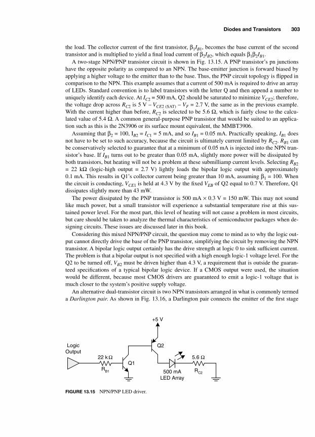
Diodes and Transistors 303
the load. The collector current of the first transistor, β1IB1, becomes the base current of the secondtransistor and is multiplied to yield a final load current of β2IB2, which equals β1β2IB1.
A two-stage NPN/PNP transistor circuit is shown in Fig. 13.15. A PNP transistor’s pn junctionshave the opposite polarity as compared to an NPN. The base-emitter junction is forward biased byapplying a higher voltage to the emitter than to the base. Thus, the PNP circuit topology is flipped incomparison to the NPN. This example assumes that a current of 500 mA is required to drive an arrayof LEDs. Standard convention is to label transistors with the letter Q and then append a number touniquely identify each device. At IC2 = 500 mA, Q2 should be saturated to minimize VCE2; therefore,the voltage drop across RC2 is 5 V – VCE2 (SAT) – VF = 2.7 V, the same as in the previous example.With the current higher than before, RC2 is selected to be 5.6 Ω, which is fairly close to the calcu-lated value of 5.4 Ω. A common general-purpose PNP transistor that would be suited to an applica-tion such as this is the 2N3906 or its surface mount equivalent, the MMBT3906.
Assuming that β2 = 100, IB2 = IC1 = 5 mA, and so IB1 = 0.05 mA. Practically speaking, IB1 doesnot have to be set to such accuracy, because the circuit is ultimately current limited by RC2. RB1 canbe conservatively selected to guarantee that at a minimum of 0.05 mA is injected into the NPN tran-sistor’s base. If IB1 turns out to be greater than 0.05 mA, slightly more power will be dissipated byboth transistors, but heating will not be a problem at these submilliamp current levels. Selecting RB2= 22 kΩ (logic-high output = 2.7 V) lightly loads the bipolar logic output with approximately0.1 mA. This results in Q1’s collector current being greater than 10 mA, assuming β1 = 100. Whenthe circuit is conducting, VCE1 is held at 4.3 V by the fixed VEB of Q2 equal to 0.7 V. Therefore, Q1dissipates slightly more than 43 mW.
The power dissipated by the PNP transistor is 500 mA × 0.3 V = 150 mW. This may not soundlike much power, but a small transistor will experience a substantial temperature rise at this sus-tained power level. For the most part, this level of heating will not cause a problem in most circuits,but care should be taken to analyze the thermal characteristics of semiconductor packages when de-signing circuits. These issues are discussed later in this book.
Considering this mixed NPN/PNP circuit, the question may come to mind as to why the logic out-put cannot directly drive the base of the PNP transistor, simplifying the circuit by removing the NPNtransistor. A bipolar logic output certainly has the drive strength at logic 0 to sink sufficient current.The problem is that a bipolar output is not specified with a high enough logic-1 voltage level. For theQ2 to be turned off, VB2 must be driven higher than 4.3 V, a requirement that is outside the guaran-teed specifications of a typical bipolar logic device. If a CMOS output were used, the situationwould be different, because most CMOS drivers are guaranteed to emit a logic-1 voltage that ismuch closer to the system’s positive supply voltage.
An alternative dual-transistor circuit is two NPN transistors arranged in what is commonly termeda Darlington pair. As shown in Fig. 13.16, a Darlington pair connects the emitter of the first stage
+5 V
RC2
5.6 Ω
500 mALED Array
LogicOutput
RB1
22 k ΩQ1
Q2
FIGURE 13.15 NPN/PNP LED driver.
-Balch.book Page 303 Thursday, May 15, 2003 3:46 PM

304 Analog Basics for Digital Systems
transistor to the base of the second. As before, the betas multiply, but now VBE is doubled to 1.4 V,because the two base-emitter junctions are in series. The higher VBE reduces the base current fromthe previous example to roughly 0.06 mA, because the same value of RB, 22 kΩ, is used. However,with an overall beta of approximately 10,000, the LED array is adequately driven.
13.6 LOGIC FUNCTIONS WITH THE BJT
The preceding circuits are binary amplifiers. In response to a small binary current input, a larger bi-nary output current is generated. Looking at these circuits another way reveals that they are very ba-sic logic gates: inverters. Consider the now familiar circuit in Fig. 13.17a. Rather than driving ahigh-current load, the output voltage is taken at the collector. When a TTL logic 0 is driven in, RCpulls the output up to logic 1, 5 V. When a TTL logic 1 is driven in, the transistor saturates and drivesthe output down to logic 0, VCE (SAT). Logic gates in bipolar ICs are more complex than this, but thebasic idea is that a simple inverter can be constructed with discrete transistors if the need arises. Thisdiscrete inverter can be transformed into a NOR gate by adding a second transistor in parallel with
RC500 mALED Array
LogicOutput
RB
22 k Ω
+5 V
5.6 Ω
FIGURE 13.16 NPN Darlington pair LED driver.
RB
4.7 k Ω
RC
+5 V
1 k Ω
InputA
OutputNOT A
(a) NOT
RB1
4.7 k Ω
RC
+5 V
1 k Ω
InputA
OutputA NOR B
(b) NOR
RB2
4.7 k ΩInput
B
FIGURE 13.17 NPN NOT and NOR gates.
-Balch.book Page 304 Thursday, May 15, 2003 3:46 PM

Diodes and Transistors 305
the one already present. In doing so, the output is logic 1 whenever both inputs are logic 0. As soonas one input is driven to logic 1, the accompanying transistor pulls the common VC output node to-ward ground and logic 0. An advantage of creating logic gates from discrete transistors is that in-compatible voltage domains can be safely bridged. In this example, the logic output is 5 Vcompatible, while the input can be almost any range of voltages as long as the transistor’s specifica-tions are not violated. This voltage conversion function would not be possible over such a widerange with normal bipolar or CMOS logic ICs.
It has been previously mentioned that TTL, or bipolar, logic outputs are asymmetrical in their 0and 1 logic level drive strengths. A TTL output, shown in Fig. 13.18, consists of a totem pole outputstage and a driver, or buffer, stage that passes the 0/1 logic function result to the output stage. It iscalled a totem pole output stage, because the vertical stack of two transistors and a diode somewhatresembles the layering of carvings on a totem pole. Classic TTL logic is composed entirely of NPNtransistors, because PNP transistors are more difficult to fabricate on an integrated circuit.
When Q1 is turned on, its emitter voltage, VE1, is fixed at 0.7 V by Q2. Q1 is driven into saturationby the logic circuit (not shown), which brings its collector voltage, VC1, down to VCE (SAT) + VE1,which is approximately equal to 0.9 V. The saturation voltage of Q1 is approximately 0.2 V, becausea sufficient current is injected into the base of Q1. This causes Q2 to saturate as well, driving an out-put level of VCE (SAT), 0.2 V or less. A logic 0 is driven strongly, because there is a direct, low-imped-ance path to ground through the saturated Q2. Turning our attention up to Q3, the transistor’s base-emitter junction would normally be forward biased when VC1 = VB3 = 0.9 V and VE3 = 0.2 V. Thepresence of the diode prevents this from happening by increasing the forward-bias threshold by 0.7V. Therefore, Q3 is in cutoff when Q2 is in saturation.
The resistors surrounding Q1 pull its collector and emitter to the respective voltage rails when Q1is turned off by the logic circuit. This causes Q2 to turn off and Q3 to turn on by raising VB3 to 5 V.When VB3 = 5 V, VE3 = 4.3 V, and the output voltage is dropped an additional 0.7 V by the diode to3.6 V when the load current is small. For small currents, Q3 remains in the active mode, and the out-put voltage is a function of the drop across the 1.6-kΩ resistor, VBE3, and VDIODE. As the load currentincreases, Q3 saturates, and the output voltage becomes a function of the drop across the 130 Ω re-sistor, VCE (SAT), and VD. The impedance from the 5-V supply to the output is greater than for thelogic-0 case, which is the reason that TTL logic drives a weaker logic 1.
+5 V
1 k Ω
1.6 k Ω
LogicOutput
130 Ω
+5 V
From LogicFunction
Q1
Q2
Q3
FIGURE 13.18 TTL driver.
-Balch.book Page 305 Thursday, May 15, 2003 3:46 PM
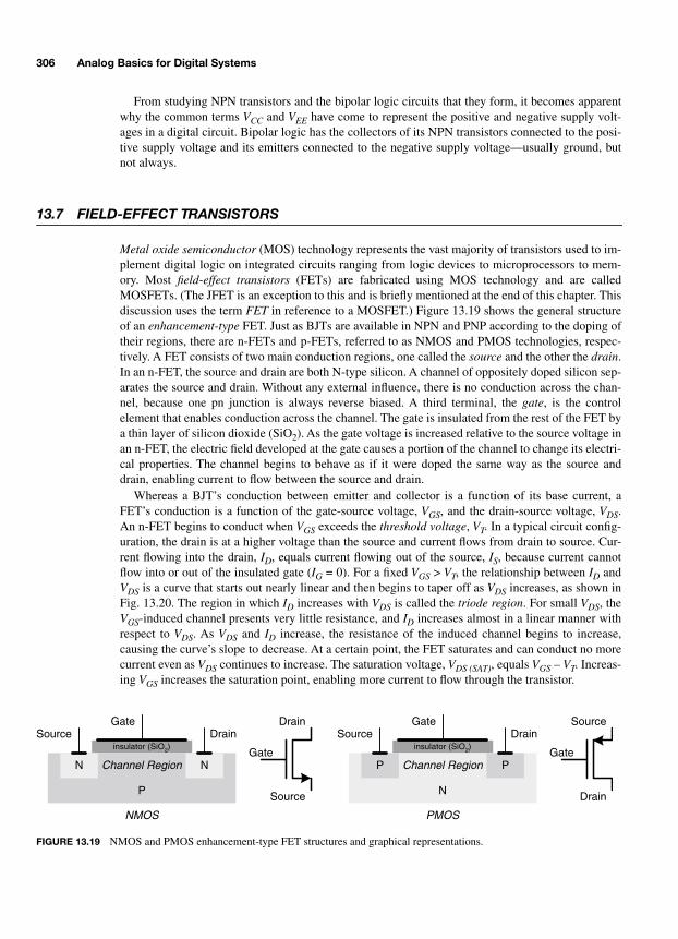
306 Analog Basics for Digital Systems
From studying NPN transistors and the bipolar logic circuits that they form, it becomes apparentwhy the common terms VCC and VEE have come to represent the positive and negative supply volt-ages in a digital circuit. Bipolar logic has the collectors of its NPN transistors connected to the posi-tive supply voltage and its emitters connected to the negative supply voltage—usually ground, butnot always.
13.7 FIELD-EFFECT TRANSISTORS
Metal oxide semiconductor (MOS) technology represents the vast majority of transistors used to im-plement digital logic on integrated circuits ranging from logic devices to microprocessors to mem-ory. Most field-effect transistors (FETs) are fabricated using MOS technology and are calledMOSFETs. (The JFET is an exception to this and is briefly mentioned at the end of this chapter. Thisdiscussion uses the term FET in reference to a MOSFET.) Figure 13.19 shows the general structureof an enhancement-type FET. Just as BJTs are available in NPN and PNP according to the doping oftheir regions, there are n-FETs and p-FETs, referred to as NMOS and PMOS technologies, respec-tively. A FET consists of two main conduction regions, one called the source and the other the drain.In an n-FET, the source and drain are both N-type silicon. A channel of oppositely doped silicon sep-arates the source and drain. Without any external influence, there is no conduction across the chan-nel, because one pn junction is always reverse biased. A third terminal, the gate, is the controlelement that enables conduction across the channel. The gate is insulated from the rest of the FET bya thin layer of silicon dioxide (SiO2). As the gate voltage is increased relative to the source voltage inan n-FET, the electric field developed at the gate causes a portion of the channel to change its electri-cal properties. The channel begins to behave as if it were doped the same way as the source anddrain, enabling current to flow between the source and drain.
Whereas a BJT’s conduction between emitter and collector is a function of its base current, aFET’s conduction is a function of the gate-source voltage, VGS, and the drain-source voltage, VDS.An n-FET begins to conduct when VGS exceeds the threshold voltage, VT. In a typical circuit config-uration, the drain is at a higher voltage than the source and current flows from drain to source. Cur-rent flowing into the drain, ID, equals current flowing out of the source, IS, because current cannotflow into or out of the insulated gate (IG = 0). For a fixed VGS > VT, the relationship between ID andVDS is a curve that starts out nearly linear and then begins to taper off as VDS increases, as shown inFig. 13.20. The region in which ID increases with VDS is called the triode region. For small VDS, theVGS-induced channel presents very little resistance, and ID increases almost in a linear manner withrespect to VDS. As VDS and ID increase, the resistance of the induced channel begins to increase,causing the curve’s slope to decrease. At a certain point, the FET saturates and can conduct no morecurrent even as VDS continues to increase. The saturation voltage, VDS (SAT), equals VGS – VT. Increas-ing VGS increases the saturation point, enabling more current to flow through the transistor.
insulator (SiO2)
P
N N
Source DrainGate
Channel RegionGate
Drain
Source
insulator (SiO2)
N
P P
Source DrainGate
Channel RegionGate
Drain
Source
NMOS PMOS
FIGURE 13.19 NMOS and PMOS enhancement-type FET structures and graphical representations.
-Balch.book Page 306 Thursday, May 15, 2003 3:46 PM
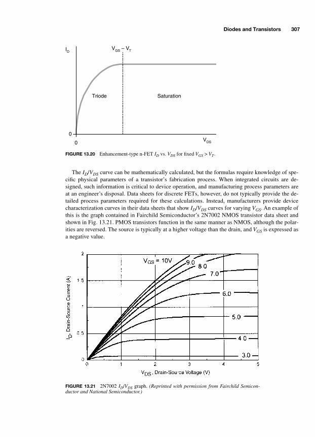
Diodes and Transistors 307
The ID/VDS curve can be mathematically calculated, but the formulas require knowledge of spe-cific physical parameters of a transistor’s fabrication process. When integrated circuits are de-signed, such information is critical to device operation, and manufacturing process parameters areat an engineer’s disposal. Data sheets for discrete FETs, however, do not typically provide the de-tailed process parameters required for these calculations. Instead, manufacturers provide devicecharacterization curves in their data sheets that show ID/VDS curves for varying VGS. An example ofthis is the graph contained in Fairchild Semiconductor’s 2N7002 NMOS transistor data sheet andshown in Fig. 13.21. PMOS transistors function in the same manner as NMOS, although the polar-ities are reversed. The source is typically at a higher voltage than the drain, and VGS is expressed asa negative value.
ID
0
0 VDS
VGS – VT
SaturationTriode
FIGURE 13.20 Enhancement-type n-FET ID vs. VDS for fixed VGS > VT.
FIGURE 13.21 2N7002 ID/VDS graph. (Reprinted with permission from Fairchild Semicon-ductor and National Semiconductor.)
-Balch.book Page 307 Thursday, May 15, 2003 3:46 PM

308 Analog Basics for Digital Systems
In the context of integrated circuits, NMOS and PMOS transistors are combined in close proxim-ity to form complementary-MOS, or CMOS, circuits. CMOS circuits are dense, consume relativelylittle power, and are easily fabricated on a silicon chip. As with any real-world device, FETs containparasitic properties, including capacitance between the gate and the source and drain, CGS and CGD.This capacitance, although small, imposes a load on the circuit that drives the gate during switching.However, when a FET is held static, such as in a DC or low-frequency circuit, the load on the drivingcircuit is essentially zero.
The 2N7002, a widely available FET, can be con-nected to drive a load as shown in Fig. 13.22 using theprevious LED example. A gate resistor is not needed,because there is no DC path to limit the currentthrough. An appropriate current limiting resistor in theload’s path may or may not be required. If the2N7002’s IDS (MAX) at the driven VGS is within theload’s specifications, the FET will serve as the currentlimiting element. A logic output, especially one operat-ing at a low voltage (e.g., 3.3 V or less) may not pro-vide sufficient VGS to drive a heavy load. This must beverified ahead of time using manufacturers’ data sheets.
Aside from the terminal capacitances already mentioned, FETs contain other parasitic character-istics that must be taken into account when designing certain types of circuits. One such characteris-tic develops when the FET’s body, the silicon that forms the channel and that surrounds the sourceand drain regions, is kept at a voltage that differs from that of the source. A typical discrete FET doesnot suffer this problem, because the body and source are electrically connected within the package.ICs, however, consist of thousands or millions of FETs wherein the bodies of each FET are not all atthe same voltages as their associated sources. This voltage, VBS, degrades the ability of the channelto conduct current and causes a FET’s VT to increase, requiring a higher VGS to conduct. More com-plete graphical representations of NMOS and PMOS FETs are shown in Fig. 13.23. Unlike the rep-resentations shown thus far, these explicitly show the FET’s body. A discrete FET usually has itsbody and source connected as shown. For the sake of simplicity, many circuit diagrams showing dis-crete FETs use the basic representation, because it is known that VBS = 0.
+5 V
RLIMIT
LogicOutput
FIGURE 13.22 NMOS transistor LED driver.
Gate
Drain
Source
BodyNMOS FET
VBS = 0
PMOS FET
Gate
Source
Drain
Body
FIGURE 13.23 Graphical representation of FET body.
-Balch.book Page 308 Thursday, May 15, 2003 3:46 PM

Diodes and Transistors 309
13.8 POWER FETS AND JFETS
Discrete FETs are used in a variety of applications. In digital systems, FETs are often found inpower supply and regulation circuitry because of the availability of low-resistance devices. A key pa-rameter of a FET used in power applications is its channel resistance between the source and drain,RDS. Per the basic power relationship, P = I2R, a FET with low RDS will waste less power and willtherefore operate at a cooler temperature. Power FET circuits can either handle more current withoutoverheating or can be made to run cooler to extend their operational life span. It is not difficult tofind power FETs with RDS well below 10 mΩ. In contrast, a BJT exhibits a VCE (SAT) that dissipatessignificant power at high currents (P = IV). The saturation voltage also increases with IC, causingmore power to be dissipated in high-power applications.
When FETs are constructed as part of an IC, they are built in a lateral configuration atop the sili-con substrate with a structure similar to what was shown earlier. Discrete FETs, however, are oftenconstructed in a vertical manner known as double-diffused MOS, or DMOS, where the source anddrain are on opposite sides of the silicon chip. The DMOS structure is shown in Fig. 13.24. DMOSsurrounds the source with a thin region of oppositely doped silicon that serves as the body throughwhich the conducting channel is induced by a voltage applied to the gate. Around the body is thesubstrate, which is doped similarly to the drain. Discrete FETs are constructed in this manner, be-cause the thin channel between the source and the substrate provides low RDS and, consequently,high current capacity with reduced power dissipation.
DMOS FETs are constructed in a manner that electrically connects the source and body regions,as shown by the metal source contacts in Fig. 13.24, so that a parasitic NPN transistor does not ariseand cause problems. A consequence of this technique is that a parasitic diode is formed between thebody and drain. Because the body is connected to the source, this is actually a source-drain diodewith the anode at the source and the cathode at the drain for an n-FET. The diode is reverse biasedunder most conditions, because an n-FET’s source is usually at a lower voltage than the drain.Therefore, VDS would have to approach –0.6 V for conduction to occur. Figure 13.24 also shows thegraphical representation of an n-type DMOS transistor with a source-drain diode. If an n-FET is de-signed such that the source is always connected to ground and the drain can never drop below 0 V,the diode has no effect. In less obvious configurations, the biasing of this inherent diode should betaken into account to ensure that current does not flow through an unintended path.
A potentially dangerous characteristic of FETs is a consequence of the insulated gate’s high inputimpedance. If a FET circuit does not create a path to the gate through which stray electrical chargecan drain away, a high voltage can build up and cause permanent damage to the device. The gate is asmall capacitor, and it is known that VCAP = Q ÷ C. Therefore, a small charge accumulating on a very
PP
N
Source
Drain
Gate
N
N Substrate
Cha
nnel
Cha
nnel
FIGURE 13.24 DMOS n-FET simplified structure and graphicalrepresentation.
-Balch.book Page 309 Thursday, May 15, 2003 3:46 PM
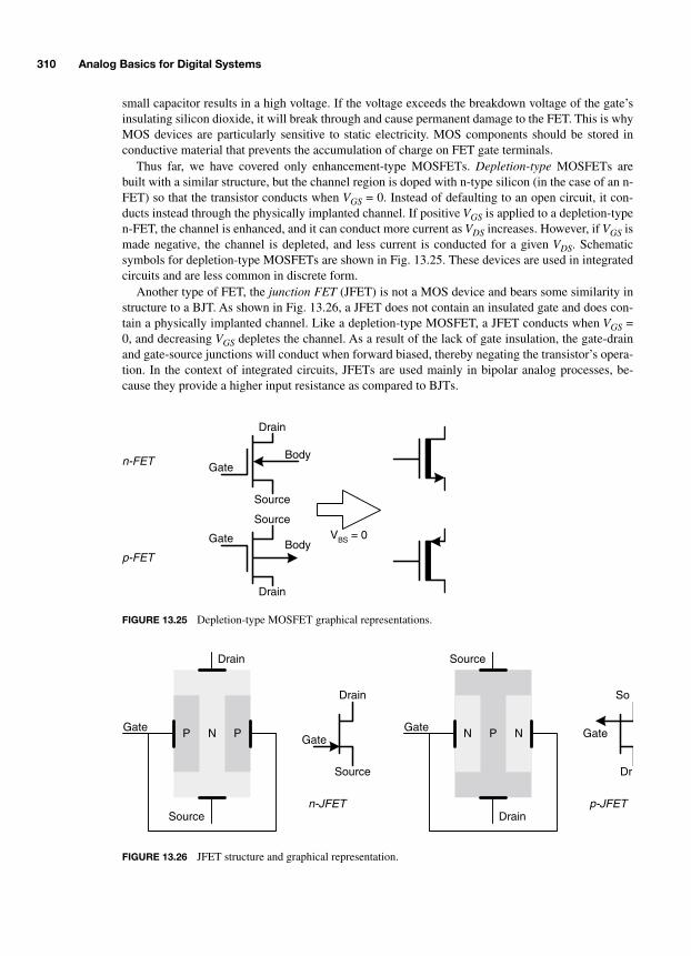
310 Analog Basics for Digital Systems
small capacitor results in a high voltage. If the voltage exceeds the breakdown voltage of the gate’sinsulating silicon dioxide, it will break through and cause permanent damage to the FET. This is whyMOS devices are particularly sensitive to static electricity. MOS components should be stored inconductive material that prevents the accumulation of charge on FET gate terminals.
Thus far, we have covered only enhancement-type MOSFETs. Depletion-type MOSFETs arebuilt with a similar structure, but the channel region is doped with n-type silicon (in the case of an n-FET) so that the transistor conducts when VGS = 0. Instead of defaulting to an open circuit, it con-ducts instead through the physically implanted channel. If positive VGS is applied to a depletion-typen-FET, the channel is enhanced, and it can conduct more current as VDS increases. However, if VGS ismade negative, the channel is depleted, and less current is conducted for a given VDS. Schematicsymbols for depletion-type MOSFETs are shown in Fig. 13.25. These devices are used in integratedcircuits and are less common in discrete form.
Another type of FET, the junction FET (JFET) is not a MOS device and bears some similarity instructure to a BJT. As shown in Fig. 13.26, a JFET does not contain an insulated gate and does con-tain a physically implanted channel. Like a depletion-type MOSFET, a JFET conducts when VGS =0, and decreasing VGS depletes the channel. As a result of the lack of gate insulation, the gate-drainand gate-source junctions will conduct when forward biased, thereby negating the transistor’s opera-tion. In the context of integrated circuits, JFETs are used mainly in bipolar analog processes, be-cause they provide a higher input resistance as compared to BJTs.
Gate
Drain
Source
Body
VBS = 0Gate
Source
Drain
Body
n-FET
p-FET
FIGURE 13.25 Depletion-type MOSFET graphical representations.
N
Source
Drain
n-JFET
P PGateGate
Drain
Source
Source
Drainp-JFET
PGate Gate
Dr
So
N N
FIGURE 13.26 JFET structure and graphical representation.
-Balch.book Page 310 Thursday, May 15, 2003 3:46 PM

311
CHAPTER 14
Operational Amplifiers
Transistors are the basic building blocks of solid-state amplifiers. Designing an amplifier using dis-crete transistors can be a substantial undertaking that requires theory outside the scope of this book.Operational amplifiers, or
op-amps,
exist to make the design of basic amplification circuits relativelyeasy. A digital engineer can use an op-amp to construct a general-purpose amplifier or active filter topreprocess an analog signal that may serve as input to the system. Comparators, which are based onop-amps, are useful in triggering events based on a signal reaching a certain threshold.
A key benefit of the op-amp is that it implements complex discrete transistor circuitry within asingle integrated circuit and presents the engineer with a straightforward three-terminal amplifierthat has well defined specifications and that can be externally configured to exhibit a wide range ofcharacteristics.
Op-amps are presented here from three basic perspectives. First, the device is introduced using anidealized model so that its basic operation can be explained clearly without involving too many si-multaneous details. The ideal op-amp is a very useful construct, because many real op-amp circuitscan be treated as being ideal, as will be demonstrated later. Fundamental op-amp circuit analysis isstepped through in detail as part of the ideal presentation. The second section brings in nonideal de-vice behavior and discusses how the idealized assumptions already introduced are affected in realcircuits. The remainder of the chapter walks through a broad array of common op-amp circuit topol-ogies with step-by-step analyses of their operation. The last of these presentations deals with the op-amp’s cousin, the comparator, and explains the important topic of hysteresis.
14.1 THE IDEAL OP-AMP
The design of amplifiers is normally most relevant in analog circuits such as those found in audioand RF communications. An amplifier is an analog circuit that outputs a signal with greater ampli-tude than what is presented to it at the input. Amplification is sometimes necessary in digital sys-tems. Amplifiers are often found at interfaces where the weak signal from a transducer (e.g.,microphone or antenna) must be strengthened for sampling by an analog-to-digital converter. Even ifa signal has sufficient amplitude, it may be desirable to scale it for better sampling resolution. Forexample, if an analog-to-digital converter accepts an input of 0 to 5 V and the incoming signalswings only between 0 and 3 V, 40 percent of the converter’s resolution will be wasted. An amplifiercan be used to scale the signal up to the full 5-V input range of the converter.
Solid-state amplifiers are constructed using transistors integrated onto a silicon chip or discretetransistors wired together on a circuit board. Amplifiers range greatly in complexity; complete ACanalysis theory and its application to discrete amplifier design are outside the scope of this book.However, the design of many general-purpose amplifiers is made easier by the availability of pre-built components called
operational amplifiers
(op-amps). Op-amps are so common that they are
-Balch.book Page 311 Thursday, May 15, 2003 3:46 PM
Copyright 2003 by The McGraw-Hill Companies, Inc. Click Here for Terms of Use.

312 Analog Basics for Digital Systems
considered to be basic building blocks in analog circuit design. An op-amp may contain dozens oftransistors, but its external interface consists of two differential inputs and an amplified output asshown in Fig. 14.1. The positive, or
noninverting
, and the negative, or
inverting
, inputs form a differ-ential voltage,
v
D
= v
+
– v
–
, that is amplified by a certain gain,
A
, at the output so that
v
O
=
Av
D
=
A
(
v
+
–
v
–
). When discussing the AC signals on which amplifiers operate, lower-case letters are usedto indicate voltages and currents by convention to distinguish them from DC voltages and currentsthat have already been shown to use capital letters.
Many of the implementation details of how an AC signal is amplified within the op-amp are hid-den from the circuit designer, requiring only an understanding of how the op-amp behaves from anexternal perspective. It is best to first explore an ideal op-amp’s operation and then take into accountthe real-world deviations from the ideal model as necessary when designing a real circuit. An idealop-amp has the following characteristics:
•
Infinite input impedance.
No current flows into or out of the inputs
•
Infinite open-loop gain.
This may sound confusing, but most op-amp circuits employ feedbackthat reduces the infinite gain to the desired level. A =
∞
simplifies op-amp circuit analysis, as willsoon be shown.
•
Infinite bandwidth.
The op-amp’s gain is constant across frequency from zero to infinity.
•
Zero output impedance.
The op-amp’s output will always be equal to
Av
D
regardless of the loadbeing driven.
These fundamental assumptions provide the engineer with a very flexible amplifier component thatcan be customized by surrounding circuitry to suit a wide range of applications. Perhaps the firstquestion that comes to mind is how an amplifier with infinite gain can be made useful. The trick is increating a
closed-loop
circuit that provides feedback from output to input to control the gain of theoverall circuit. Without a feedback path, an
open-loop
op-amp circuit would, in fact, exhibit veryhigh gain to the point of grossly distorting most types of signals. Consider the basic
noninverting
closed-loop op-amp circuit in Fig. 14.2. While the signal is injected into the positive input, the op-amp’s output feeds back to the negative input through the resistor network formed by R1 and R2.
Based on the assumption of infinite input impedance, a basic resistor divider expression for
v
–
canbe written based solely on the output voltage,
v
O
, and the two resistors.
Knowing that
v
O
=
Av
D
=
A
(
v
+
–
v
–
), this expression can be used to reveal a relationship betweenthe input voltage,
v
I
, and
v
O
.
+
–
Noninverting Input
Inverting Input
Output = AvDvD
v+
v–
FIGURE 14.1 Op-amp graphical representation.
v– vOR1
R1 R2+--------------------=
vO A v+ v––( ) AvI A vOR1
R1 R2+--------------------–= =
-Balch.book Page 312 Thursday, May 15, 2003 3:46 PM
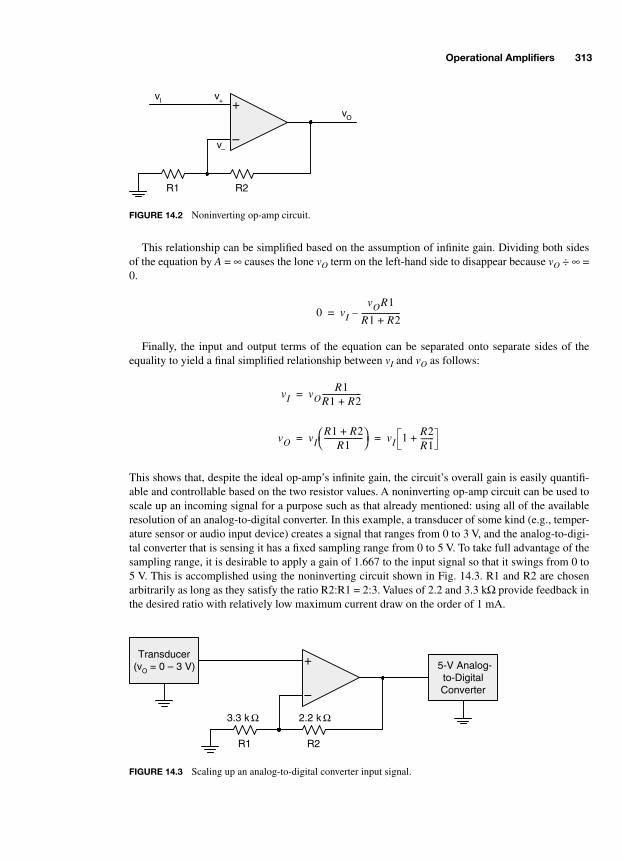
Operational Amplifiers 313
This relationship can be simplified based on the assumption of infinite gain. Dividing both sidesof the equation by
A
=
∞
causes the lone
v
O
term on the left-hand side to disappear because
v
O
÷
∞
=0.
Finally, the input and output terms of the equation can be separated onto separate sides of theequality to yield a final simplified relationship between
v
I
and
v
O
as follows:
This shows that, despite the ideal op-amp’s infinite gain, the circuit’s overall gain is easily quantifi-able and controllable based on the two resistor values. A noninverting op-amp circuit can be used toscale up an incoming signal for a purpose such as that already mentioned: using all of the availableresolution of an analog-to-digital converter. In this example, a transducer of some kind (e.g., temper-ature sensor or audio input device) creates a signal that ranges from 0 to 3 V, and the analog-to-digi-tal converter that is sensing it has a fixed sampling range from 0 to 5 V. To take full advantage of thesampling range, it is desirable to apply a gain of 1.667 to the input signal so that it swings from 0 to5 V. This is accomplished using the noninverting circuit shown in Fig. 14.3. R1 and R2 are chosenarbitrarily as long as they satisfy the ratio R2:R1 = 2:3. Values of 2.2 and 3.3 k
Ω
provide feedback inthe desired ratio with relatively low maximum current draw on the order of 1 mA.
+
–
R1 R2
v+
v–
vI
vO
FIGURE 14.2 Noninverting op-amp circuit.
0 vI
vOR1
R1 R2+--------------------–=
vI vOR1
R1 R2+--------------------=
vO vIR1 R2+
R1--------------------
vI 1 R2R1-------+= =
+
–
R1 R2
3.3 k Ω 2.2 k Ω
Transducer(vO = 0 – 3 V) 5-V Analog-
to-DigitalConverter
FIGURE 14.3 Scaling up an analog-to-digital converter input signal.
-Balch.book Page 313 Thursday, May 15, 2003 3:46 PM
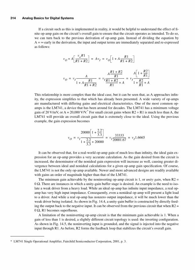
314 Analog Basics for Digital Systems
If a circuit such as this is implemented in reality, it would be helpful to understand the effect of fi-nite op-amp gain on the circuit’s overall gain to ensure that the circuit operates as intended. To do so,we can turn back to the previous derivation of op-amp gain. Instead of dividing the equation byA =
∞
early in the derivation, the input and output terms are immediately separated and re-expressedas follows:
This relationship is more complex than the ideal case, but it can be seen that, as A approaches infin-ity, the expression simplifies to that which has already been presented. A wide variety of op-ampsare manufactured with differing gains and electrical characteristics. One of the most common op-amps is the LM741, a device that has been around for decades. The LM741 has a minimum voltagegain of 20 V/mV, or A = 20,000 V/V.
*
For small circuit gains where R2 ÷ R1 is much less than A, theLM741 will provide an overall circuit gain that is extremely close to the ideal. Using the previousexample, the gain expression becomes
It can be observed that, for a real-world op-amp gain of much less than infinity, the ideal gain ex-pression for an op-amp provides a very accurate calculation. As the gain desired from the circuit isincreased, the denominator of the nonideal gain expression will increase as well, causing greater di-vergence between ideal and nonideal calculations for a given op-amp gain specification. Of course,the LM741 is not the only op-amp available. Newer and more advanced designs are readily availablewith gains an order of magnitude higher than that of the LM741.
The minimum gain achievable by the noninverting op-amp circuit is 1, or
unity gain
, when R2 =0
Ω
. There are instances in which a unity-gain buffer stage is desired. An example is the need to iso-late a weak driver from a heavy load. While an ideal op-amp has infinite input impedance, a real op-amp has very high input impedance. Consequently, even a nonideal op-amp will present a light loadto a driver. And while a real op-amp has nonzero output impedance, it will be much lower than theweak driver being isolated. As shown in Fig. 14.4, a unity-gain buffer is constructed by directly feed-ing the output back to the negative input. It can be observed from the previous circuit that when R2 =0
Ω
, R1 becomes superfluous.A limitation of the noninverting op-amp circuit is that the minimum gain achievable is 1. When a
gain of less than 1 is desired, a slightly different circuit topology is used: the inverting configuration.As shown in Fig. 14.5, the noninverting input is grounded, and the signal is injected into the negativeinput through R1. As before, R2 forms the feedback loop that stabilizes the circuit’s overall gain.
* LM741 Single Operational Amplifier, Fairchild Semiconductor Corporation, 2001, p. 3.
vO AvoR1
R1 R2+--------------------+ AvI vO 1 A
R1R1 R2+--------------------+= =
vO vIA
1 AR1
R1 R2+--------------------+
---------------------------------- vI
AR1 R2+
R1--------------------
R1 R2+R1
-------------------- A+------------------------------- vI
A 1 R2R1-------+
1 R2R1------- A+ +
---------------------------= = =
vO vI
20000 1 2.23.3-------+
1 2.23.3------- 20000+ +
-------------------------------------- vI33333
20001.67---------------------- vI1.6665= = =
-Balch.book Page 314 Thursday, May 15, 2003 3:46 PM
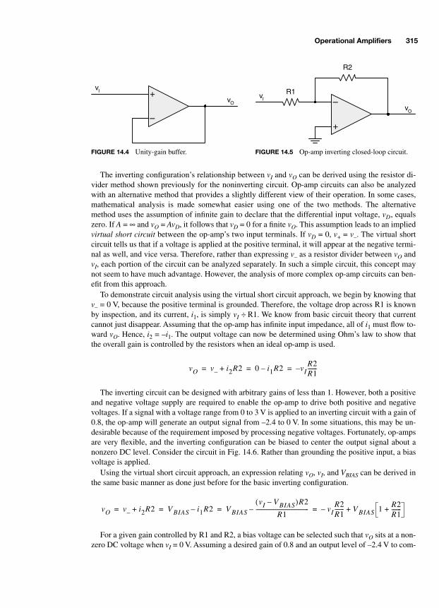
Operational Amplifiers 315
The inverting configuration’s relationship between vI and vO can be derived using the resistor di-vider method shown previously for the noninverting circuit. Op-amp circuits can also be analyzedwith an alternative method that provides a slightly different view of their operation. In some cases,mathematical analysis is made somewhat easier using one of the two methods. The alternativemethod uses the assumption of infinite gain to declare that the differential input voltage, vD, equalszero. If A = ∞ and vO = AvD, it follows that vD = 0 for a finite vO. This assumption leads to an impliedvirtual short circuit between the op-amp’s two input terminals. If vD = 0, v+ = v–. The virtual shortcircuit tells us that if a voltage is applied at the positive terminal, it will appear at the negative termi-nal as well, and vice versa. Therefore, rather than expressing v– as a resistor divider between vO andvI, each portion of the circuit can be analyzed separately. In such a simple circuit, this concept maynot seem to have much advantage. However, the analysis of more complex op-amp circuits can ben-efit from this approach.
To demonstrate circuit analysis using the virtual short circuit approach, we begin by knowing thatv– = 0 V, because the positive terminal is grounded. Therefore, the voltage drop across R1 is knownby inspection, and its current, i1, is simply vI ÷ R1. We know from basic circuit theory that currentcannot just disappear. Assuming that the op-amp has infinite input impedance, all of i1 must flow to-ward vO. Hence, i2 = –i1. The output voltage can now be determined using Ohm’s law to show thatthe overall gain is controlled by the resistors when an ideal op-amp is used.
The inverting circuit can be designed with arbitrary gains of less than 1. However, both a positiveand negative voltage supply are required to enable the op-amp to drive both positive and negativevoltages. If a signal with a voltage range from 0 to 3 V is applied to an inverting circuit with a gain of0.8, the op-amp will generate an output signal from –2.4 to 0 V. In some situations, this may be un-desirable because of the requirement imposed by processing negative voltages. Fortunately, op-ampsare very flexible, and the inverting configuration can be biased to center the output signal about anonzero DC level. Consider the circuit in Fig. 14.6. Rather than grounding the positive input, a biasvoltage is applied.
Using the virtual short circuit approach, an expression relating vO, vI, and VBIAS can be derived inthe same basic manner as done just before for the basic inverting configuration.
For a given gain controlled by R1 and R2, a bias voltage can be selected such that vO sits at a non-zero DC voltage when vI = 0 V. Assuming a desired gain of 0.8 and an output level of –2.4 V to com-
+
–
vI
vO
+
–R1
R2
vI
vO
FIGURE 14.4 Unity-gain buffer. FIGURE 14.5 Op-amp inverting closed-loop circuit.
vO v– i2R2+ 0 i1R2– vI–R2R1-------= = =
vO v– i2R2+ V BIAS i1R2– V BIAS
vI V BIAS–( )R2
R1---------------------------------------– vI
R2R1-------– V BIAS 1 R2
R1-------++= = = =
-Balch.book Page 315 Thursday, May 15, 2003 3:46 PM

316 Analog Basics for Digital Systems
pensate for, VBIAS = 2.4 V ÷ 1.8 = 1.33 V. The specific bias voltage required may not be readily avail-able. In these circumstances, a voltage divider may be employed at the positive input to produce anarbitrary bias voltage from a common supply such as +5 or +3.3 V. This scheme enables an op-ampto be used in the inverting configuration with a single supply voltage as long as the bias voltage issufficient to produce a minimum output voltage of zero.
14.2 CHARACTERISTICS OF REAL OP-AMPS
Real op-amps are subject to the same laws of physics that cause nonideal behavior in all types of de-vices. The degree to which these deviations negatively affect a system varies according to the spe-cific circuit. Op-amp manufacturers provide detailed data sheets to accompany their products,because many parameters must be characterized to enable proper circuit design. Fairchild Semicon-ductor’s venerable LM741 serves as a useful example with which to explore real op-amp specifica-tions. A portion of the LM741 data sheet is shown in Fig. 14.7.
Nonideal input characteristics are specified in the top portion of the LM741’s data sheet. Inputoffset voltage, VIO, is a DC error introduced by the op-amp’s internal circuitry that manifests itself asan applied differential voltage between the two inputs. Assuming an ideal op-amp, VIO appears as avoltage source applied by the external circuitry. If 0 V is applied to the op-amp, the input voltage isactually equivalent to VIO. If a real op-amp is powered on in an open-loop configuration, its verylarge, though not infinite, open-loop gain can cause the output voltage to saturate because of the non-zero input voltage due to VIO. The LM741’s open-loop gain, shown as GV in the data sheet, is be-tween 20 and 200 V/mV. With VIO = 2 mV, the output voltage is forced to its limit. Of course, op-amps are not generally used in an open-loop configuration. Figure 14.8 shows a common op-ampconfiguration in which the circuit’s two inputs are grounded. The inputs are grounded to simplifyanalysis of VIO effects in the absence of an input signal. When an input signal is present, the VIO ef-fects are added to the input/output transfer function. VIO is represented as a separate voltage sourceapplied to an ideal op-amp. Because VIO appears as a differential voltage, the op-amp’s output is ap-proximated by the idealized closed-loop noninverting gain relationship: VO = VIO (1 + R2 ÷ R1).This is essentially the same situation as the biased inverting op-amp circuit shown in Fig. 14.6, al-though the bias voltage is undesired. Therefore, the input offset voltage is amplified along with sig-nals that are applied to the circuit.
It can be difficult to compensate for input offset voltage, because each individual op-amp has adifferent polarity and magnitude of VIO, making it impossible to design a circuit with a fixed com-pensation factor suitable for all devices. Additionally, VIO changes with temperature. Depending on
DC BiasVoltage
+
–R1
R2
VBIAS
VBIAS
vI
vO
FIGURE 14.6 Biased inverting op-amp circuit.
-Balch.book Page 316 Thursday, May 15, 2003 3:46 PM
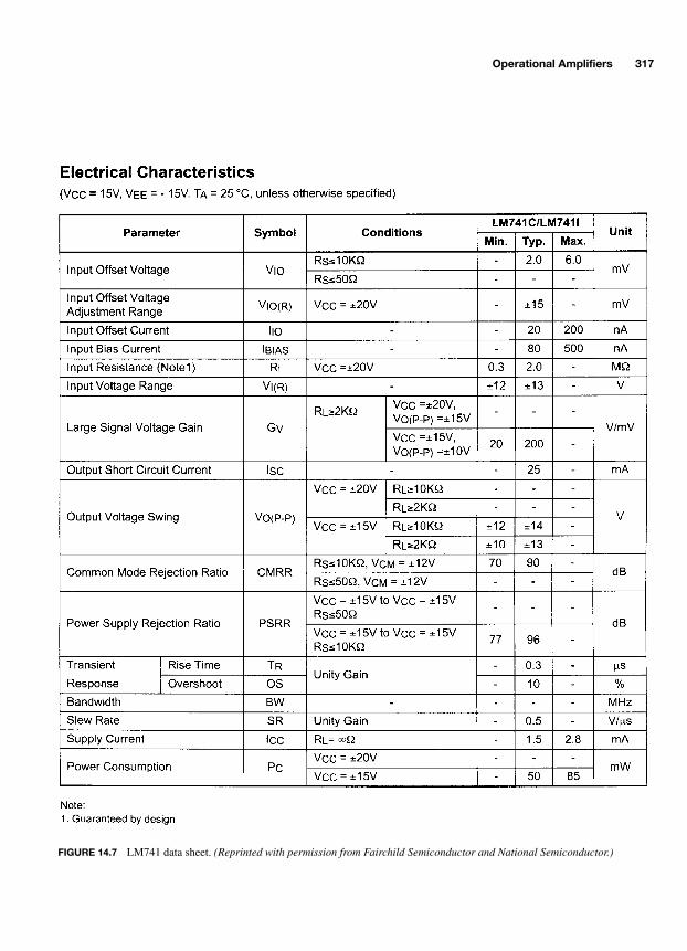
Operational Amplifiers 317
FIGURE 14.7 LM741 data sheet. (Reprinted with permission from Fairchild Semiconductor and National Semiconductor.)
-Balch.book Page 317 Thursday, May 15, 2003 3:46 PM

318 Analog Basics for Digital Systems
the accuracy of the op-amp, the manufacturer will specify VIO at room temperature (25°C) and atother temperature thresholds and provide coefficients or charts that relate the change in VIO to tem-perature. Some op-amps, including the LM741, include compensation inputs that can be used tonull-out the input offset error with external resistors. There is a limit to the practicality of this ap-proach, however, resulting from temperature effects and the variation between components.
VIO may not cause much trouble in an op-amp circuit with small gain, because a few millivolts ofoffset may be relatively insignificant as compared to several volts of actual signal. However, high-gain op-amp circuits that handle inputs with amplitudes in the millivolt range may be substantiallydegraded by VIO effects. It may be desirable to AC-couple the op-amp’s input when the frequenciesof interest are high enough to make AC coupling feasible. The inverting circuit in Fig. 14.9 uses a ca-pacitor to block a DC path to the op-amp’s negative input. Because VIO is a DC offset, the gain of thecircuit is analyzed at DC to determine the amplification of VIO. The impedance of the capacitor isideally infinite at DC, resulting in unity gain for VIO. For this circuit to function properly, the inputfrequency must be sufficiently high to not be attenuated by the highpass filter created by the seriesresistor and capacitor. The circuit exhibits a cutoff frequency where fC = 1 ÷ 2πCR1. Therefore, fre-quencies much larger than fC will be amplified by the idealized gain factor, –(R2 ÷ R1), when the ca-pacitor essentially becomes a short circuit between the input and R1. The result is high gain at thefrequencies of interest, yielding volts of output magnitude with only millivolts of VIO error resultingfrom unity gain at DC.
Another parameter that relates to input offset voltage is the power supply rejection ratio (PSRR).The PSRR relates changes in the supply voltage to changes in VIO. As the power rails fluctuate dur-ing normal operation, they influence the internal characteristics of the op-amp. PSRR is expressed indecibels as
The LM741’s minimum PSRR is specified at 77 dB. To ease arithmetic for the sake of discussion,we can round up to 80 dB and calculate PSRR = 10,000. This means that for every 1-V change in thesupply voltage, VIO changes by 100 µV. We know that VIO is amplified by the gain of a DC-coupledcircuit from the example in Fig. 14.8, indicating that a high-gain circuit is more susceptible to PSRReffects. PSRR declines with increasing frequency, making an op-amp more susceptible to powersupply fluctuations.
Nonzero input currents are another source of inaccuracy in op-amp circuit, because real op-ampsdo not have infinite input resistance. Small nonzero currents flow into and out of the op-amp’s in-
VIO
+
–R1
R2
VIO
VIO vO
FIGURE 14.8 Analysis of input offset voltage.
PSRR 20∆V CC
∆V IO---------------log=
-Balch.book Page 318 Thursday, May 15, 2003 3:46 PM
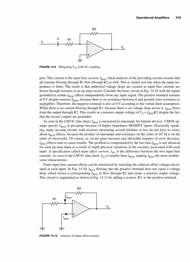
Operational Amplifiers 319
puts. This current is the input bias current, IBIAS. Ideal analyses of the preceding circuits assume thatall currents flowing through R1 flow through R2 as well. This is clearly not true when the input im-pedance is finite. The result is that undesired voltage drops are created as input bias currents aredrawn through resistors in an op-amp circuit. Consider the basic circuit in Fig. 14.10 with the inputsgrounded to isolate IBIAS effects independently from any input signal. The positive terminal remainsat 0 V despite nonzero IBIAS, because there is no resistance between it and ground (wire resistance isnegligible). Therefore, the negative terminal is also at 0 V according to the virtual short assumption.While there is no current flowing through R1, because there is no voltage drop across it, IBIAS flowsfrom the output through R2. This results in a nonzero output voltage of VO = IBIASR2 despite the factthat the circuit’s inputs are grounded.
As seen in the LM741 data sheet, IBIAS is measured in nanoamps for bipolar devices. CMOS op-amps specify IBIAS in picoamps because of higher impedance MOSFET inputs. Practically speak-ing, many op-amp circuits with resistors measuring several kilohms or less do not have to worryabout IBIAS effects, because the product of nanoamps and resistance on the order of 103 Ω is on theorder of microvolts. Of course, as circuit gains increase and allowable margins of error decrease,IBIAS effects start to cause trouble. The problem is compounded by the fact that IBIAS is not identicalfor each op-amp input as a result of slight physical variations in the circuitry associated with eachinput. A specification called input offset current, IIO, is the difference between the two input biascurrents. As seen in the LM741 data sheet, IIO is smaller than IBIAS, making IBIAS the more trouble-some characteristic.
Finite input bias current effects can be minimized by matching the induced offset voltages devel-oped at each input. In Fig. 14.10, IBIAS flowing into the positive terminal does not cause a voltagedrop, which forces a corresponding IBIAS to flow through R2 and create a nonzero output voltage.This circuit is augmented as shown in Fig. 14.11 by adding a resistor, R3, to the positive terminal.
+
–R1
R2
CvI
vO
FIGURE 14.9 Mitigating VIO with AC coupling.
+
–R1
R2
IBIAS
IBIAS
vO
FIGURE 14.10 Analysis of input offset current.
-Balch.book Page 319 Thursday, May 15, 2003 3:46 PM
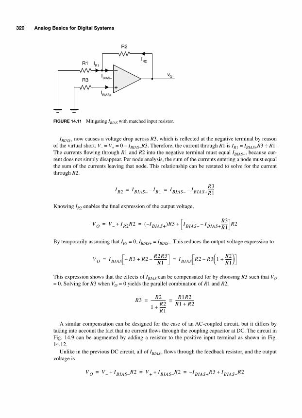
320 Analog Basics for Digital Systems
IBIAS+ now causes a voltage drop across R3, which is reflected at the negative terminal by reasonof the virtual short. V– = V+ = 0 – IBIAS+R3. Therefore, the current through R1 is IR1 = IBIAS+R3 ÷ R1.The currents flowing through R1 and R2 into the negative terminal must equal IBIAS–, because cur-rent does not simply disappear. Per node analysis, the sum of the currents entering a node must equalthe sum of the currents leaving that node. This relationship can be restated to solve for the currentthrough R2.
Knowing IR2 enables the final expression of the output voltage,
By temporarily assuming that IIO = 0, IBIAS+ = IBIAS–. This reduces the output voltage expression to
This expression shows that the effects of IBIAS can be compensated for by choosing R3 such that VO= 0. Solving for R3 when VO = 0 yields the parallel combination of R1 and R2,
A similar compensation can be designed for the case of an AC-coupled circuit, but it differs bytaking into account the fact that no current flows through the coupling capacitor at DC. The circuit inFig. 14.9 can be augmented by adding a resistor to the positive input terminal as shown in Fig.14.12.
Unlike in the previous DC circuit, all of IBIAS– flows through the feedback resistor, and the outputvoltage is
+
–R1
R2
IBIAS+
IBIAS–R3
IR2
vO
IR1
FIGURE 14.11 Mitigating IBIAS with matched input resistor.
IR2 IBIAS– IR1– IBIAS– IBIAS+R3R1-------–= =
V O V – IR2R2+ IBIAS+–( )R3 IBIAS– IBIAS+R3R1-------– R2+= =
V O IBIAS R3– R2 R2R3R1
--------------–+ IBIAS R2 R3 1 R2R1-------+
–= =
R3 R2
1 R2R1-------+
---------------- R1R2R1 R2+--------------------= =
V O V – IBIAS–R2+ V + IBIAS–R2+ IBIAS+– R3 IBIAS–R2+= = =
-Balch.book Page 320 Thursday, May 15, 2003 3:46 PM

Operational Amplifiers 321
If the input bias currents are assumed to be equal, selecting R3 = R2 nulls out the effects of IBIASin the AC coupled circuit.
Unfortunately, IIO remains a problem in both the DC and AC circuits, although it is a problem ofless magnitude than that of uncompensated IBIAS. In Fig. 14.10, it was observed that uncompensatedIBIAS results in VO = IBIASR2. Once IBIAS has been compensated for by the inclusion of a resistor inthe positive input terminal, IIO effectively becomes the uncompensated IBIAS term, resulting in VO =IIOR2. Again, IIO as specified in nanoamps and picoamps may not present much problem for manycircuits in which the feedback resistor, R2, is relatively small.
Continuing down the LM741 data sheet, additional physical realities are observed. Input voltagelevels are limited by the chip’s supply voltages. As the input levels approach the supply voltages, theop-amp’s ability to deliver ideal performance diminishes. Supply voltages also relate to the outputvoltage swing of the op-amp. Many op-amps are unable to drive rail-to-rail. In other words, if an op-amp’s supply voltages are ±15 V, the range of output voltages may be only ±14 V under lightlyloaded conditions (10 kΩ in the LM741’s case). As the output current demand increases, the op-amp’s guaranteed drive level is diminished. Modern op-amps are available with a wide range of out-put drive strengths and characteristics. Rail-to-rail op-amps guarantee the ability to drive to withinmillivolts of either voltage supply at their rated drive current.
An op-amp is a differential amplifier with an ideal transfer function of vO =AvD. According to thissimple relationship, only the voltage difference between the positive and negative terminals has anybearing on the output voltage. The same vD results when v+ = 0.02 V and v– = 0.01 V as when v+ =10.02 V and v– = 10.01 V. Ideally, the common-mode voltage, that voltage applied to both terminals,has no effect upon the output voltage. The first and second pairs of input levels have common-modevoltages, vCM, of 0.01 and 10.01 V, respectively. Both pairs of inputs may be within the specified in-put range of a particular op-amp, but each pair will cause somewhat different behavior. The reasonfor this is that a real op-amp does not contain a perfect differential amplifier. The internal amplifierhas some sensitivity to the common-mode signal that is applied to it.
If the inputs of an op-amp are tied together and a common-mode voltage is applied, there will besome nonzero output response even if the circuit has already been compensated for input offset er-rors. An op-amp has a finite common-mode gain associated with it such that vO =ACMvCM indepen-dent of the differential gain, A. Manufacturers define a common-mode rejection ratio (CMRR) thatspecifies the ratio of differential to common mode gain,
CMRR is expressed in decibels to more easily represent large ratios. A high CMRR indicates thatA >> ACM, which means that undesired effects due to common-mode input voltages are reduced.
+
–R1
R2C
IBIAS+
R3
IBIAS–
vO
FIGURE 14.12 Mitigating IBIAS in an AC coupled circuit.
CMRR 20 AACM------------log=
-Balch.book Page 321 Thursday, May 15, 2003 3:46 PM

322 Analog Basics for Digital Systems
Fairchild’s LM741 has a minimum CMRR of 70 dB when |vCM| < 12 V. The total output voltage ofan op-amp is the sum of the differential and common-mode gains: vO =AvD + ACMvCM. If CMRR is A÷ ACM, then ACM = A ÷ CMRR and
This relationship shows how higher CMRR yields behavior that is closer to the ideal differential am-plifier. CMRR is specified by manufacturers at DC and is sufficiently large that most applicationsoperating at low frequencies are not adversely affected by common-mode input voltages within thestated specifications. As with many specifications, CMRR gets worse as the frequency increases.Graphs are typically included in data sheets that relate CMRR to frequency.
Figure 14.13 shows how finite CMRR affects inverting and noninverting circuit topologies differ-ently. An unbiased inverting circuit has the op-amp’s positive input grounded, which results in a DCpotential of 0 V at the negative input as well because of the virtual short assumption. This creates acommon-mode input voltage of approximately 0 V, thus minimizing the effects of CMRR. If the in-verting circuit is biased, a common-mode voltage approximately equal to the bias voltage results,with CMRR impact. Similarly, a noninverting circuit injects a signal into the positive input, resultingin a common-mode voltage approximately equal to the input signal.
Finite CMRR influence on a noninverting circuit can be quantified as a function of vD withoutvCM, because vD ≈ vCM. To isolate the CMRR effects, the real noninverting op-amp circuit can be
vO AvDA
CMRR-----------------vCM+ A vD
vCM
CMRR-----------------+= =
Unbiased Inverting Circuit
+
–R1
R2
VCM = 0V
VBIAS
+
–R1
R2
VCM = VBIAS
Biased Inverting Circuit
+
–
R1 R2
VCM = vI
Noninverting Circuit
vO
vI
vO
vI
vO
vI
FIGURE 14.13 Common-mode input vs. circuit topology.
-Balch.book Page 322 Thursday, May 15, 2003 3:46 PM

Operational Amplifiers 323
modeled as the combination of an ideal op-amp with an offset voltage caused by finite CMRR,vCMRR , as shown in Fig. 14.14. An ideal op-amp multiplies the input voltage, vCMRR, by its differen-tial gain, A, to yield an output voltage. Likewise, the nonideal op-amp being modeled multiplies thecommon-mode input voltage, vCM ≈ vD ≈ vI, by its common mode gain to yield an output voltage.Therefore, AvCMRR = ACMvI. This equivalency can be restated as vCMRR = ACMvI ÷ A, which is actu-ally a function of CMRR: vCMRR = vI ÷ CMRR.
With CMRR now modeled as an input that is a function of CMRR and the actual input voltage,the ideal op-amp model can be treated as a block to which the actual input signal is presented asshown in Fig. 14.15.
The total output voltage is the sum of the input voltage and vCMRR passed through the ideal op-amp as separate terms,
As with input offset voltage, CMRR effects are more pronounced at higher circuit gains.
+
–R1
R2
VCMRR=VI
CMRR
vO
FIGURE 14.14 Modeling CMRR effects in a noninvert-ing circuit.
+
–R1
R2
VCMRR
VI
VCMRR+VI
vO
FIGURE 14.15 CMRR model with signal input.
vO vI vCMRR+[ ] 1 R2R1-------+ vI
vI
CMRR-----------------+ 1 R2
R1-------+ vI 1 1
CMRR-----------------+ 1 R2
R1-------+= = =
-Balch.book Page 323 Thursday, May 15, 2003 3:46 PM

324 Analog Basics for Digital Systems
14.3 BANDWIDTH LIMITATIONS
An op-amp’s ability to amplify a signal is a direct function of the frequencies involved. The maxi-mum frequency at which an op-amp provides useful performance can be characterized in multipleways. Manufacturers provide a variety of related specifications to assist in this task. First, there is thegain-bandwidth product (GBW), also referred to as bandwidth (BW). As the name implies, GBWspecifies a gain at a certain frequency. As the frequency of operation is decreased, the gain increases,and vice versa. Most op-amp data sheets provide either a bandwidth number, sometimes specified asthe unity-gain bandwidth, or a chart that relates gain to frequency. The large-signal voltage gain ofthe LM741 remains relatively constant for frequencies only under 10 Hz (not kHz!). It is called“large-signal,” because the response is essentially at DC; “small-signal” would denote practical op-erating frequencies that are typically orders of magnitude higher. Near 10 Hz, the gain rolls off at therate of –20 dB per decade and reaches unity gain, 0 dB, near 1 MHz. Above 1 MHz, the LM741’sgain rapidly drops off. Keep in mind, however, that this is the LM741’s open-loop response. When aclosed-loop circuit is formed, the gain is substantially lowered, thereby increasing the circuit’s us-able bandwidth over which the gain remains constant.
Figure 14.16 shows an approximate gain versus frequency curve for an older bipolar op-amp suchas the LM741. The gain of the open-loop op-amp is approximately 100 dB below 10 Hz. Observethat, if the closed-loop gain is set at 10 (20 dB), the constant gain portion of the curve drops by ap-proximately 80 dB, which correlates to four decades of frequency. Therefore, the closed-loop band-width increases to 10 Hz multiplied by four decades, or 100 kHz. Put another way, 100 dB equals100,000. The gain-bandwidth product is approximately 100,000 × 10 Hz = 1 MHz. If a closed-loopgain of 10 is used, the bandwidth is 1 MHz ÷ 10 = 100 kHz.
Two other interrelated frequency metrics are slew rate and full-power bandwidth. These specifica-tions enable an engineer to determine whether a signal will be distorted by the op-amp based on thesignal’s frequency and amplitude. Slew rate defines the rate at which the op-amp can change its out-put voltage. The LM741’s specified slew rate is 0.5 V/µs. If the desired output signal has a compo-nent that changes voltage faster than the slew rate, the op-amp will not be able to fully reproduce thesignal and is said to be slew-rate limited. An example of slew-rate limiting is shown in Fig. 14.17,where the desired sine wave output, a pure signal with a single frequency, is converted to a trianglewaveform that transitions at the op-amp’s maximum slew rate.
–20
0
Gain(dB)
Frequency (Hz)
1 10 100 1k
20
40
60
80
100
120
10k 100k 1M 10M
Open-Loop Gain
Closed-Loop Gain
FIGURE 14.16 Typical gain vs. frequency curve.
-Balch.book Page 324 Thursday, May 15, 2003 3:46 PM
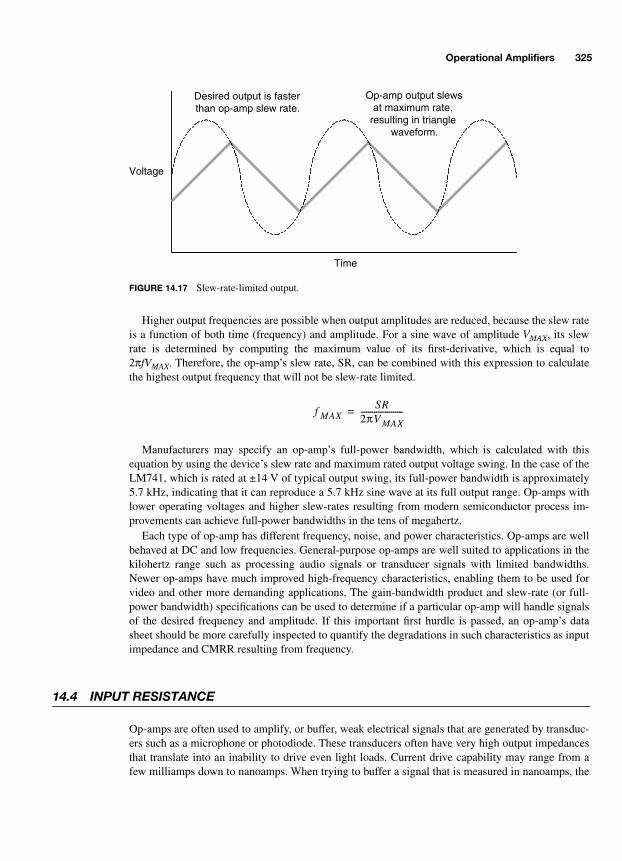
Operational Amplifiers 325
Higher output frequencies are possible when output amplitudes are reduced, because the slew rateis a function of both time (frequency) and amplitude. For a sine wave of amplitude VMAX, its slewrate is determined by computing the maximum value of its first-derivative, which is equal to2πfVMAX. Therefore, the op-amp’s slew rate, SR, can be combined with this expression to calculatethe highest output frequency that will not be slew-rate limited.
Manufacturers may specify an op-amp’s full-power bandwidth, which is calculated with thisequation by using the device’s slew rate and maximum rated output voltage swing. In the case of theLM741, which is rated at ±14 V of typical output swing, its full-power bandwidth is approximately5.7 kHz, indicating that it can reproduce a 5.7 kHz sine wave at its full output range. Op-amps withlower operating voltages and higher slew-rates resulting from modern semiconductor process im-provements can achieve full-power bandwidths in the tens of megahertz.
Each type of op-amp has different frequency, noise, and power characteristics. Op-amps are wellbehaved at DC and low frequencies. General-purpose op-amps are well suited to applications in thekilohertz range such as processing audio signals or transducer signals with limited bandwidths.Newer op-amps have much improved high-frequency characteristics, enabling them to be used forvideo and other more demanding applications. The gain-bandwidth product and slew-rate (or full-power bandwidth) specifications can be used to determine if a particular op-amp will handle signalsof the desired frequency and amplitude. If this important first hurdle is passed, an op-amp’s datasheet should be more carefully inspected to quantify the degradations in such characteristics as inputimpedance and CMRR resulting from frequency.
14.4 INPUT RESISTANCE
Op-amps are often used to amplify, or buffer, weak electrical signals that are generated by transduc-ers such as a microphone or photodiode. These transducers often have very high output impedancesthat translate into an inability to drive even light loads. Current drive capability may range from afew milliamps down to nanoamps. When trying to buffer a signal that is measured in nanoamps, the
Time
Voltage
Desired output is fasterthan op-amp slew rate.
Op-amp output slewsat maximum rate,
resulting in trianglewaveform.
FIGURE 14.17 Slew-rate-limited output.
f MAXSR
2πV MAX----------------------=
-Balch.book Page 325 Thursday, May 15, 2003 3:46 PM
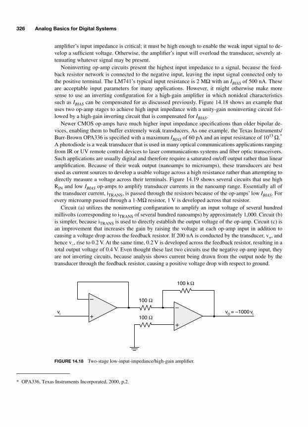
326 Analog Basics for Digital Systems
amplifier’s input impedance is critical; it must be high enough to enable the weak input signal to de-velop a sufficient voltage. Otherwise, the amplifier’s input will overload the transducer, severely at-tenuating whatever signal may be present.
Noninverting op-amp circuits present the highest input impedance to a signal, because the feed-back resistor network is connected to the negative input, leaving the input signal connected only tothe positive terminal. The LM741’s typical input resistance is 2 MΩ with an IBIAS of 500 nA. Theseare acceptable input parameters for many applications. However, it might otherwise make moresense to use an inverting configuration for a high-gain amplifier in which nonideal characteristicssuch as IBIAS can be compensated for as discussed previously. Figure 14.18 shows an example thatuses two op-amp stages to achieve high input impedance with a unity-gain noninverting circuit fol-lowed by a high-gain inverting circuit that is compensated for IBIAS.
Newer CMOS op-amps have much higher input impedance specifications than older bipolar de-vices, enabling them to buffer extremely weak transducers. As one example, the Texas Instruments/Burr-Brown OPA336 is specified with a maximum IBIAS of 60 pA and an input resistance of 1013 Ω.*
A photodiode is a weak transducer that is used in many optical communications applications rangingfrom IR or UV remote control devices to laser communications systems and fiber optic transceivers.Such applications are usually digital and therefore require a saturated on/off output rather than linearamplification. Because of their weak output (nanoamps to microamps), these transducers are bestused as current sources to develop a usable voltage across a high resistance rather than attempting todirectly measure a voltage across their terminals. Figure 14.19 shows several circuits that use highRIN and low IBIAS op-amps to amplify transducer currents in the nanoamp range. Essentially all ofthe transducer current, iTRANS, is passed through the resistors because of the op-amps’ low IBIAS. Forevery microamp passed through a 1-MΩ resistor, 1 V is developed across that resistor.
Circuit (a) utilizes the noninverting configuration to amplify an input voltage of several hundredmillivolts (corresponding to iTRANS of several hundred nanoamps) by approximately 1,000. Circuit (b)is simpler, because iTRANS is used to directly establish the output voltage of the op-amp. Circuit (c) isan improvement that increases the gain by raising the voltage at each op-amp input in addition tocausing a voltage drop across the feedback resistor. If 200 nA is conducted by the transducer, v+, andhence v–, rise to 0.2 V. At the same time, 0.2 V is developed across the feedback resistor, resulting in atotal output voltage of 0.4 V. Even thought these last two circuits use the negative op-amp input, theyare not inverting circuits, because analysis shows current being drawn from the output node by thetransducer through the feedback resistor, causing a positive voltage drop with respect to ground.
* OPA336, Texas Instruments Incorporated, 2000, p.2.
+
–100 Ω
100 k Ω
+
–
100 ΩvI vO = –1000 vI
FIGURE 14.18 Two-stage low-input-impedance/high-gain amplifier.
-Balch.book Page 326 Thursday, May 15, 2003 3:46 PM
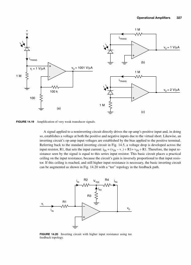
Operational Amplifiers 327
A signal applied to a noninverting circuit directly drives the op-amp’s positive input and, in doingso, establishes a voltage at both the positive and negative inputs due to the virtual short. Likewise, aninverting circuit’s op-amp input voltages are established by the bias applied to the positive terminal.Referring back to the standard inverting circuit in Fig. 14.5, a voltage drop is developed across theinput resistor, R1, that sets the input current: iIN = (vIN – v–) ÷ R1= vIN ÷ R1. Therefore, the input re-sistance seen by the signal is equal to this series input resistor. This basic circuit places a practicalceiling on the input resistance, because the circuit’s gain is inversely proportional to that input resis-tor. If this ceiling is reached, and still higher input resistance is necessary, the basic inverting circuitcan be augmented as shown in Fig. 14.20 with a “tee” topology in the feedback path.
+
-
100 k
1 M
100
+V
vI = 1 V/µA
iTRANS
+
-
1 M
iTRANS
+
-
1 M
iTRANS
1 M(a)
(b)
(c)
vO = 1001 V/µA
vO = 2 V/µA
vO = 1 V/µA
FIGURE 14.19 Amplification of very weak transducer signals.
+
–R1
R2 R4
R3
VTEE
iIN
iIN
iR3
iR4
vI
vO
FIGURE 14.20 Inverting circuit with higher input resistance using teefeedback topology.
-Balch.book Page 327 Thursday, May 15, 2003 3:46 PM
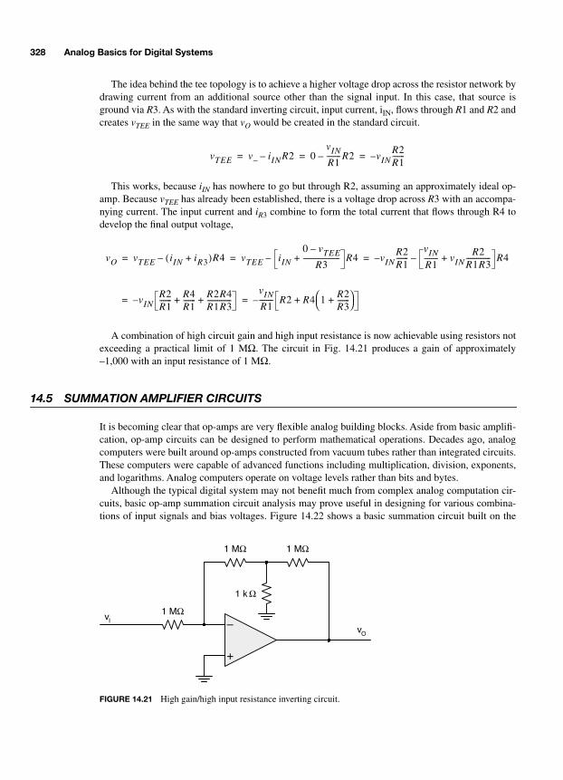
328 Analog Basics for Digital Systems
The idea behind the tee topology is to achieve a higher voltage drop across the resistor network bydrawing current from an additional source other than the signal input. In this case, that source isground via R3. As with the standard inverting circuit, input current, iIN, flows through R1 and R2 andcreates vTEE in the same way that vO would be created in the standard circuit.
This works, because iIN has nowhere to go but through R2, assuming an approximately ideal op-amp. Because vTEE has already been established, there is a voltage drop across R3 with an accompa-nying current. The input current and iR3 combine to form the total current that flows through R4 todevelop the final output voltage,
A combination of high circuit gain and high input resistance is now achievable using resistors notexceeding a practical limit of 1 MΩ. The circuit in Fig. 14.21 produces a gain of approximately–1,000 with an input resistance of 1 MΩ.
14.5 SUMMATION AMPLIFIER CIRCUITS
It is becoming clear that op-amps are very flexible analog building blocks. Aside from basic amplifi-cation, op-amp circuits can be designed to perform mathematical operations. Decades ago, analogcomputers were built around op-amps constructed from vacuum tubes rather than integrated circuits.These computers were capable of advanced functions including multiplication, division, exponents,and logarithms. Analog computers operate on voltage levels rather than bits and bytes.
Although the typical digital system may not benefit much from complex analog computation cir-cuits, basic op-amp summation circuit analysis may prove useful in designing for various combina-tions of input signals and bias voltages. Figure 14.22 shows a basic summation circuit built on the
vTEE v– iIN R2– 0vIN
R1--------R2– vIN
R2R1-------–= = =
vO vTEE iIN iR3+( )R4– vTEE iIN
0 vTEE–
R3---------------------+ R4– vIN
R2R1-------
vIN
R1-------- vIN
R2R1R3--------------+ R4––= = =
vINR2R1------- R4
R1------- R2R4
R1R3--------------+ +–
vIN
R1-------- R2 R4 1 R2
R3-------+
+–= =
+
–1 MΩ
1 k Ω
1 MΩ 1 MΩ
vI
vO
FIGURE 14.21 High gain/high input resistance inverting circuit.
-Balch.book Page 328 Thursday, May 15, 2003 3:46 PM

Operational Amplifiers 329
inverting topology. Each input is unaffected by the others, because the negative terminal is always at0 V by reason of the virtual short. Therefore, each input resistor contributes an input current compo-nent determined by Ohm’s law. These currents add and collectively pass through the feedback resis-tor to create an output voltage.
A weighted summation can be designed by individually selecting input resistors according to theapplication requirements. If the input resistors are all equal, the gain ratios for each input signal areequal, and the summation is balanced.
Similarly, a noninverting circuit can be used to combine multiple input voltages without the –1factor as shown in Fig. 14.23. Although usually referred to as a noninverting summer, this is more ofan averaging circuit than a summer. The input voltages are averaged by the input resistor network,and this average level is then multiplied by the gain of the noninverting circuit.
Analyzing the input resistor network can be difficult without a common circuit-analysis trick thatrelies on the principle of superposition. Superposition works with a linear transfer function that re-lates an output to multiple inputs multiplied by some gain factor. For example, two signals, V1 andV2, add together and are multiplied to yield an output voltage: VO = A(V1 + V2). By the principle ofsuperposition, the input terms can be broken up, computed separately, and then recombined at theoutput to yield a final expression: VO1 = AV1 and VO2 = AV2, thus VO = VO1 + VO2 = A(V1 + V2). Su-perposition works only when the transfer function is linear.
+
–RIN1
RF
RIN3
RIN2vO
v1
v3
v2
FIGURE 14.22 Summation circuit.
vO
RF
RIN--------- v1 v2 v3+ +[ ]–=
+
–
RIN1
R2
RIN3
RIN2
R1
vO
v1
v3
v2
FIGURE 14.23 Noninverting summation circuit.
-Balch.book Page 329 Thursday, May 15, 2003 3:46 PM
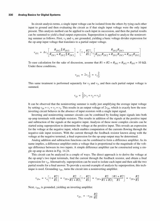
330 Analog Basics for Digital Systems
In circuit analysis terms, a single input voltage can be isolated from the others by tying each otherinput to ground and then evaluating the circuit as if that single input voltage were the only inputpresent. This analysis method can be applied to each input in succession, and then the partial resultscan be summed to yield a final output expression. Superposition is applied to analyze the noninvert-ing summer as follows. First, v2 and v3 are grounded, yielding a basic voltage divider expression forthe op-amp input voltage that translates to a partial output voltage.
To ease calculation for the sake of discussion, assume that R1 = R2 = RIN1 = RIN2 = RIN3 = 10 kΩ.Under these conditions,
This same treatment is performed separately for v2 and v3, and then each partial output voltage issummed.
It can be observed that the noninverting summer is really just amplifying the average input voltageby setting vIN = v1 = v2 = v3. This results in an output voltage of 2vIN, which is exactly how the non-inverting circuit behaves in the absence of input resistors with a single input signal.
Inverting and noninverting summer circuits can be combined by feeding input signals into bothop-amp terminals with multiple resistors. This results in addition of the signals at the positive inputand subtraction of the signals at the negative input. Analysis of these more complex circuits can bestarted using superposition to determine the voltage at the positive input. This reveals an expressionfor the voltage at the negative input, which enables computation of the currents flowing through thenegative-side input resistors. With the current through the feedback resistor known along with thevoltage at the negative terminal, a final expression for the op-amp output may be determined.
Analog addition and subtraction functions can be combined to form a difference amplifier. As itsname implies, a difference amplifier emits a voltage that is proportional to the magnitude of the volt-age difference between its two inputs. A simple difference amplifier can be constructed using a sin-gle op-amp as shown in Fig. 14.24.
This circuit can be analyzed in a couple of ways. The direct approach is to derive the voltage atthe op-amp’s two input terminals, find the current through the feedback resistor, and obtain a finalexpression for vO. Alternatively, superposition can be used to isolate each input and then add the twopartial results for a final answer. To provide a second example of analysis by superposition, this tech-nique is used. Grounding vIN– turns the circuit into a noninverting amplifier.
Next, vIN+ is grounded, yielding an inverting amplifier.
vO1 Av1
RIN 2 RIN 3||
RIN 1 RIN 2 RIN 3||+
------------------------------------------------- 1 R2R1-------+ v1
RIN 2RIN 3
RIN 1RIN 2 RIN 1RIN 3 RIN 2RIN 3+ +-----------------------------------------------------------------------------------------= =
vO1 2v113--- v1
23---= =
vO23--- v1 v2 v3+ +[ ]=
vO+ v+ 1 R2R1-------+ vIN +
R2R1 R2+-------------------- 1 R2
R1-------+ vIN +
R2R1 R2+-------------------- R1 R2+
R1-------------------- vIN +
R2R1-------= = = =
vO– vIN –R2R1-------–=
-Balch.book Page 330 Thursday, May 15, 2003 3:46 PM
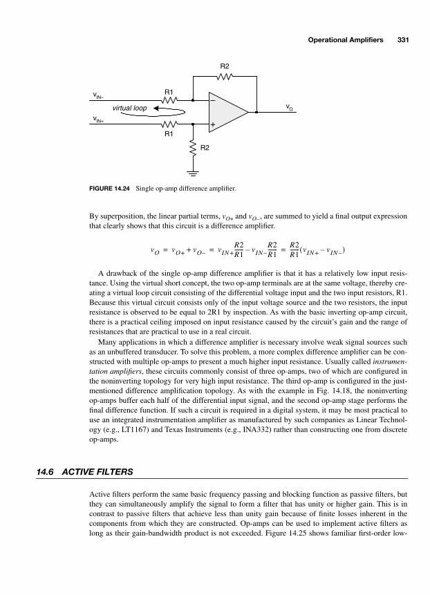
Operational Amplifiers 331
By superposition, the linear partial terms, vO+ and vO–, are summed to yield a final output expressionthat clearly shows that this circuit is a difference amplifier.
A drawback of the single op-amp difference amplifier is that it has a relatively low input resis-tance. Using the virtual short concept, the two op-amp terminals are at the same voltage, thereby cre-ating a virtual loop circuit consisting of the differential voltage input and the two input resistors, R1.Because this virtual circuit consists only of the input voltage source and the two resistors, the inputresistance is observed to be equal to 2R1 by inspection. As with the basic inverting op-amp circuit,there is a practical ceiling imposed on input resistance caused by the circuit’s gain and the range ofresistances that are practical to use in a real circuit.
Many applications in which a difference amplifier is necessary involve weak signal sources suchas an unbuffered transducer. To solve this problem, a more complex difference amplifier can be con-structed with multiple op-amps to present a much higher input resistance. Usually called instrumen-tation amplifiers, these circuits commonly consist of three op-amps, two of which are configured inthe noninverting topology for very high input resistance. The third op-amp is configured in the just-mentioned difference amplification topology. As with the example in Fig. 14.18, the noninvertingop-amps buffer each half of the differential input signal, and the second op-amp stage performs thefinal difference function. If such a circuit is required in a digital system, it may be most practical touse an integrated instrumentation amplifier as manufactured by such companies as Linear Technol-ogy (e.g., LT1167) and Texas Instruments (e.g., INA332) rather than constructing one from discreteop-amps.
14.6 ACTIVE FILTERS
Active filters perform the same basic frequency passing and blocking function as passive filters, butthey can simultaneously amplify the signal to form a filter that has unity or higher gain. This is incontrast to passive filters that achieve less than unity gain because of finite losses inherent in thecomponents from which they are constructed. Op-amps can be used to implement active filters aslong as their gain-bandwidth product is not exceeded. Figure 14.25 shows familiar first-order low-
+
–R1
R2
R2
R1
virtual loop vO
vIN+
vIN–
FIGURE 14.24 Single op-amp difference amplifier.
vO vO+ vO–+ vIN +R2R1------- vIN –
R2R1-------–
R2R1------- vIN + vIN ––( )= = =
-Balch.book Page 331 Thursday, May 15, 2003 3:46 PM
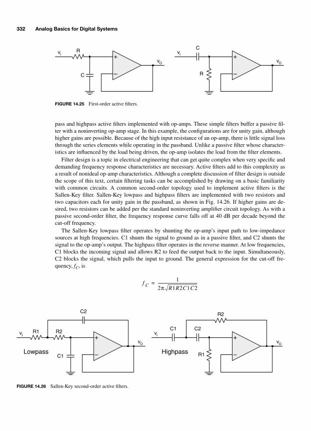
332 Analog Basics for Digital Systems
pass and highpass active filters implemented with op-amps. These simple filters buffer a passive fil-ter with a noninverting op-amp stage. In this example, the configurations are for unity gain, althoughhigher gains are possible. Because of the high input resistance of an op-amp, there is little signal lossthrough the series elements while operating in the passband. Unlike a passive filter whose character-istics are influenced by the load being driven, the op-amp isolates the load from the filter elements.
Filter design is a topic in electrical engineering that can get quite complex when very specific anddemanding frequency response characteristics are necessary. Active filters add to this complexity asa result of nonideal op-amp characteristics. Although a complete discussion of filter design is outsidethe scope of this text, certain filtering tasks can be accomplished by drawing on a basic familiaritywith common circuits. A common second-order topology used to implement active filters is theSallen-Key filter. Sallen-Key lowpass and highpass filters are implemented with two resistors andtwo capacitors each for unity gain in the passband, as shown in Fig. 14.26. If higher gains are de-sired, two resistors can be added per the standard noninverting amplifier circuit topology. As with apassive second-order filter, the frequency response curve falls off at 40 dB per decade beyond thecut-off frequency.
The Sallen-Key lowpass filter operates by shunting the op-amp’s input path to low-impedancesources at high frequencies. C1 shunts the signal to ground as in a passive filter, and C2 shunts thesignal to the op-amp’s output. The highpass filter operates in the reverse manner. At low frequencies,C1 blocks the incoming signal and allows R2 to feed the output back to the input. Simultaneously,C2 blocks the signal, which pulls the input to ground. The general expression for the cut-off fre-quency, fC, is
+
–
R
RC
+
–
C
vO
vI
vO
vI
FIGURE 14.25 First-order active filters.
+
–
R2
R1C1
+
–
C2R1
C2
C1
R2
vO
vI
vO
vI
Lowpass Highpass
FIGURE 14.26 Sallen-Key second-order active filters.
f C1
2π R1R2C1C2-----------------------------------------=
-Balch.book Page 332 Thursday, May 15, 2003 3:46 PM

Operational Amplifiers 333
In many cases, it is convenient to set R1 = R2 and C1 = C2, in which case fC is given by
Aside from providing amplification, a benefit of using op-amps to build filter stages is that multi-ple stages can be cascaded to implement more advanced filters. The presence of the op-amp in eachstage isolates one stage’s filter components from the other, thereby preserving the desired responseof each filter circuit. Higher-order lowpass and highpass filters with sharper roll-off responses can beconstructed in this manner. Alternatively, bandpass or band-reject filters can be designed by cascad-ing lowpass and highpass stages as needed.
14.7 COMPARATORS AND HYSTERESIS
Each op-amp circuit discussed so far is closed loop because of the need to moderate the op-amp’slarge open-loop gain and, simultaneously, to increase the circuit’s bandwidth to a practical frequencyrange. Analog electronics begins to turn digital when the concern is no longer about maintaining alinear relationship between a circuit’s input and output signals. Comparators are a key crossoverfunction between the analog and digital worlds. The job of a comparator is to assert its output whenthe input rises above a certain threshold and deassert its output when the input falls below a thresh-old. A comparator implements a binary step function as shown in Fig. 14.27. This transfer functionis decidedly nonlinear and is produced using a differential amplifier with very large gain.
If an op-amp is operated in an open-loop topology, it can be adapted to serve as a comparator.Figure 14.28 shows an op-amp or comparator with its negative input connected to a fixed thresholdvoltage, VREF, and its positive input being driven by the circuit’s input signal. As long as the inputsignal remains below VREF, the differential voltage is negative, and the output is driven to the lowervoltage rail (ground, in this case). As the input signal rises above VREF, a minute differential voltageis amplified by the tremendous open-loop gain, resulting in a nearly perfect step function.
Op-amps can be used as comparators, but dedicated comparator ICs have long been available.Comparators and op-amps share various internal similarities. Their common heritage is obvious
f C1
2πRC---------------=
00 VREF
vO
vI
vO(MAX)
FIGURE 14.27 Generic comparator transfer function.
-Balch.book Page 333 Thursday, May 15, 2003 3:46 PM
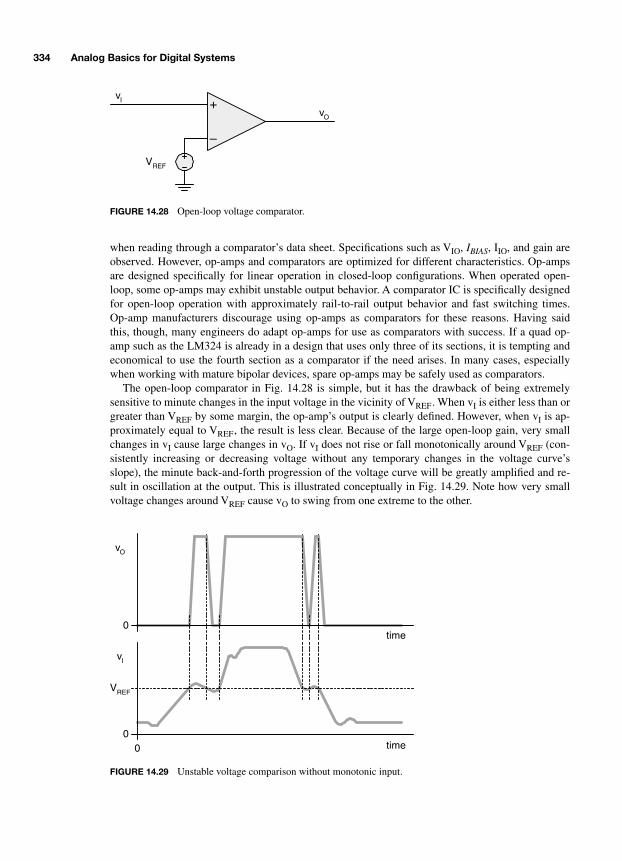
334 Analog Basics for Digital Systems
when reading through a comparator’s data sheet. Specifications such as VIO, IBIAS, IIO, and gain areobserved. However, op-amps and comparators are optimized for different characteristics. Op-ampsare designed specifically for linear operation in closed-loop configurations. When operated open-loop, some op-amps may exhibit unstable output behavior. A comparator IC is specifically designedfor open-loop operation with approximately rail-to-rail output behavior and fast switching times.Op-amp manufacturers discourage using op-amps as comparators for these reasons. Having saidthis, though, many engineers do adapt op-amps for use as comparators with success. If a quad op-amp such as the LM324 is already in a design that uses only three of its sections, it is tempting andeconomical to use the fourth section as a comparator if the need arises. In many cases, especiallywhen working with mature bipolar devices, spare op-amps may be safely used as comparators.
The open-loop comparator in Fig. 14.28 is simple, but it has the drawback of being extremelysensitive to minute changes in the input voltage in the vicinity of VREF. When vI is either less than orgreater than VREF by some margin, the op-amp’s output is clearly defined. However, when vI is ap-proximately equal to VREF, the result is less clear. Because of the large open-loop gain, very smallchanges in vI cause large changes in vO. If vI does not rise or fall monotonically around VREF (con-sistently increasing or decreasing voltage without any temporary changes in the voltage curve’sslope), the minute back-and-forth progression of the voltage curve will be greatly amplified and re-sult in oscillation at the output. This is illustrated conceptually in Fig. 14.29. Note how very smallvoltage changes around VREF cause vO to swing from one extreme to the other.
+
–
VREF
vO
vI
FIGURE 14.28 Open-loop voltage comparator.
00 time
0time
VREF
vO
vI
FIGURE 14.29 Unstable voltage comparison without monotonic input.
-Balch.book Page 334 Thursday, May 15, 2003 3:46 PM

Operational Amplifiers 335
It can be difficult to achieve a perfectly monotonic signal because of ambient noise in a system. Ifthe signal can be guaranteed to rise and fall quickly, the window of opportunity for noise to triggeran undesired response at VREF is limited. This is how the majority of signals in a digital system oper-ate. The rise and fall times are relatively fast, and the signals remain stable at logic-high and logic-low voltages. Problems do arise, however, when excessive noise or other signal integrity issues man-ifest themselves by causing nonmonotonic signal transitions. In a purely digital context, such prob-lems can be solved with proper engineering solutions to reduce and shield noise and signal integrityproblems. Most real-world analog signals do not behave in a clean binary fashion, which is why theyoften require analog circuits including op-amps and comparators to properly interface with digitalsystems.
Threshold comparison can be improved by adding hysteresis to an otherwise open-loop voltagecomparator. Hysteresis is the application of two thresholds to stabilize a comparator so that it does notchange its state with minute changes in the input voltage. Stabilization is desirable in situationswherein the applied voltage hovers near the threshold voltage for more than a brief span of time asseen in Fig. 14.29. Rather than a single threshold, separate low-to-high, VTLH, and high-to-low, VTHL,thresholds are designed. VTLH is higher than VTHL, as demonstrated in Fig. 14.30, where a muchcleaner output is obtained as compared to the previous case. Note that the hysteresis created by thetwo thresholds prevents the comparator’s output from returning to logic 0 when the input declinesslightly after triggering a logic-1 output. Similarly, the input’s nonmonotonic falling-edge does notcause the output to bounce, because the hysteresis is chosen to be greater than the local perturbation.
A hysteresis loop is a common means of representing the two distinct thresholds governing the in-put/output transfer function. Figure 14.31 shows that, when the input is starting from the low side,the high threshold is used to trigger an output state transition. As soon as the input crosses the highthreshold, the output goes high, and the low threshold is now applied to the input comparison. No-tice the advantage here. Once the input rises above the high threshold, a lower threshold is instantlysubstituted. This means that, if the input signal wanders and declines slightly, it is still above thelower threshold, and the output is unaffected. For the output to return low, the input must now fallbelow the low threshold. And as soon as this occurs, the high threshold is again activated so that theinput must rise significantly before an output stage change will occur.
00 time
0time
VTHL
VTLH
vO
vI
FIGURE 14.30 Effect of hysteresis on nonmonotonic input signal.
-Balch.book Page 335 Thursday, May 15, 2003 3:46 PM
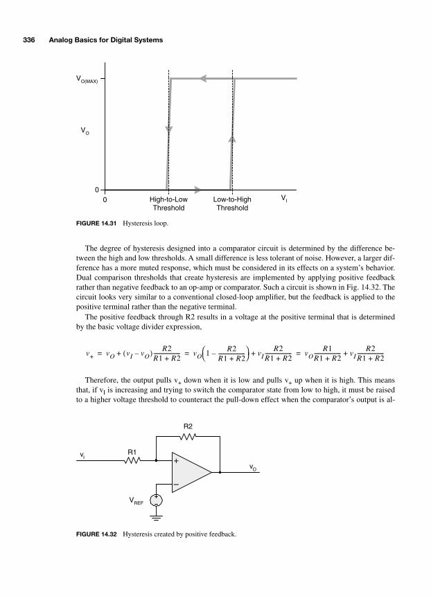
336 Analog Basics for Digital Systems
The degree of hysteresis designed into a comparator circuit is determined by the difference be-tween the high and low thresholds. A small difference is less tolerant of noise. However, a larger dif-ference has a more muted response, which must be considered in its effects on a system’s behavior.Dual comparison thresholds that create hysteresis are implemented by applying positive feedbackrather than negative feedback to an op-amp or comparator. Such a circuit is shown in Fig. 14.32. Thecircuit looks very similar to a conventional closed-loop amplifier, but the feedback is applied to thepositive terminal rather than the negative terminal.
The positive feedback through R2 results in a voltage at the positive terminal that is determinedby the basic voltage divider expression,
Therefore, the output pulls v+ down when it is low and pulls v+ up when it is high. This meansthat, if vI is increasing and trying to switch the comparator state from low to high, it must be raisedto a higher voltage threshold to counteract the pull-down effect when the comparator’s output is al-
VO
00 VIHigh-to-Low
Threshold
VO(MAX)
Low-to-HighThreshold
FIGURE 14.31 Hysteresis loop.
+
–
R1
R2
VREF
vO
vI
FIGURE 14.32 Hysteresis created by positive feedback.
v+ vO vI vO–( ) R2R1 R2+--------------------+ vO 1 R2
R1 R2+--------------------–
vIR2
R1 R2+--------------------+ vO
R1R1 R2+-------------------- vI
R2R1 R2+--------------------+= = =
-Balch.book Page 336 Thursday, May 15, 2003 3:46 PM
Operational Amplifiers 337
ready low. Similarly, vI must be reduced to a lower voltage threshold to counteract the pull-up effectwhen the output is already high.
Another benefit of hysteresis is that it “snaps” the comparator input voltage above or below VREFonce the output state transition is triggered. This forces what might otherwise be a gradually risinginput signal into a sharp edge that improves the switching time of the comparator’s output. Any timespent in a region of linear amplification as a result of vI ≈ VREF is minimized in favor of a rapid tran-sition to saturation in either the high or low output state.
The voltage at the positive terminal must be brought to VREF to cause a comparator state change.Therefore, the general relationships for the low-to-high and high-to-low thresholds, VTLH and VTHL,can be written by substituting VREF for v+ and the appropriate threshold for vI.
and
These relationships assume an ideal comparator that has zero input bias current. Real-world effectsof IBIAS can be reduced by using resistors that are not too large. If hundreds of microamps or a milli-amp are designed to flow through the R1/R2 resistor network, the nanoamps of input bias currentwill likely introduce negligible error into the system.
To illustrate the application of hysteresis in a real circuit, consider a common bipolar comparator,the LM311, connected such that it drives an approximate output range of 0 V (VOL) to 5 V (VOH). Itis desired to convert an incoming analog signal ranging from 0 to 3 V into a digital output. The half-way threshold of 1.5 V is chosen to differentiate between logical 1 and 0. However, it is known thatthe input signal can have noise of up to 500 mV peak-to-peak (p-p) superimposed on it. This meansthat a signal that is just over 1.5 V at one moment in time can abruptly drop to near 1 V a short whilelater. We do not want the LM311’s output to swing every time a 500-mV noise spike happens to co-incide with the rising and falling of the 3-V input signal. Therefore, at least 500 mV of hysteresisshould be designed into the circuit.
It is decided to design in 600 mV of hysteresis for some added margin. Rather than establishing asingle 1.5-V threshold for low-to-high and high-to-low triggering, two thresholds of 1.5 + 0.3 V and1.5 – 0.3 V are desired, which combine to provide 600 mV of hysteresis. This configuration requiresthe input to rise above 1.8 V to be recognized as a logic 1 and requires the input to fall below 1.2 Vto be recognized as a logic 0. Even if 500 mV of noise hits the input just after it reaches 1.8 V, the re-sulting 1.3 V level will be too high to trigger a return to logic 0.
The first design task is to calculate the ratio between the input and feedback resistors, R1 and R2.Recall that hysteresis is the difference between VTLH and VTHL. The previously derived expressionsfor VTHL and VTHL can be simplified for this circuit, because VOH and VOL are already known.
and
Subtracting the two thresholds yields a relationship that can be used to solve for R1 and R2.
It follows that R1 = 0.12R2. Because it is the ratio between R1 and R2 that is important rather thantheir actual values, these numbers can be multiplied by 10,000 to yield R1 = 1.2 kΩ and R2 = 10 kΩ,which are standard 5 percent tolerance resistance values. If more accurate 1 percent resistors are de-sired, R1 would be chosen as 1.21 kΩ, which is the closest 1 percent standard value.
V TLH V REFR1 R2+
R2-------------------- V OL
R1R2-------–= V THL V REF
R1 R2+R2
-------------------- V OHR1R2-------–=
V TLH V REFR1 R2+
R2--------------------= V THL V REF
R1 R2+R2
-------------------- 5R1R2-------–=
V TLH V THL– V REFR1 R2+
R2-------------------- V REF
R1 R2+R2
-------------------- 5R1R2-------+– 5
R1R2------- 0.6 V= = =
-Balch.book Page 337 Thursday, May 15, 2003 3:46 PM

338 Analog Basics for Digital Systems
With the resistors determined, the next step is to calculate the required reference voltage toachieve the desired thresholds. Using the slightly simpler expression for VTLH provides the followingresult:
, VREF = 1.61 V
Because 1.61 V is not a particularly standard voltage, it can be obtained using a voltage dividerresistor network. The math can be checked by verifying that the selected values for VREF, R1, and R2also produce the desired VTHL.
Certain digital interface applications benefit from off-the-shelf 7400 logic gates with built-in hys-teresis. A common industry term for a circuit employing hysteresis is the Schmitt trigger. Devicesemploying Schmitt triggers include the 74xx14 hex inverter and the 74xx132 quad NAND. Thegraphical symbol used to denote Schmitt trigger logic inputs is the hysteresis loop placed within astandard logic gate representation, two examples of which are shown in Fig. 14.33. The 74LS14 and74LS132 Schmitt trigger devices are members of the common 74LS bipolar logic family. Each ofthese devices is specified with 1.4 = VTLH = 1.9 and 0.5 = VTHL = 1.0.* These specifications guaran-tee a minimum hysteresis of 0.4 V, making them suitable for handling many noisy signals.
* 74LS14, Fairchild Semiconductor Corporation, 2000, p. 2.
V TLH 1.8 V REFR1 R2+
R2-------------------- V REF 1.12( )= = =
V THL V REFR1 R2+
R2-------------------- 5
R1R2-------– 1.61 1.12( ) 5 0.12( )– 1.2 V= = =
FIGURE 14.33 Graphical representation of Schmitt trigger in-verter and NAND gate.
-Balch.book Page 338 Thursday, May 15, 2003 3:46 PM
339
CHAPTER 15
Analog Interfaces for Digital Systems
The intersection of analog and digital worlds has given rise to a tremendously broad range of appli-cations for digital systems. Digital cellular telephones, enhanced radar systems, and computerizedengine controls are just a few modern benefits enabled by data conversion circuits. Analog-to-digitaland digital-to-analog converters enable computers to interact with the real world by representingcontinuous analog signals as sequences of discrete numbers.
The first portion of this chapter discusses topics including quantization, sampling rate, and theNyquist frequency. These concepts form the foundation of data conversion and enable an engineer toevaluate the conversion requirements for individual applications. Specific analog-to-digital and digi-tal-to-analog conversion techniques are presented in the next portion of the chapter. Selecting thecorrect data conversion IC is a combination of identifying the application requirements and thenfinding a device that matches these specifications.
Following the initial evaluation process, designing an effective data conversion circuit at the sys-tem level varies in complexity with how accurate the conversion must be. Some applications withmoderate accuracy requirements can be implemented without much difficulty by following the man-ufacturer’s recommended connection diagrams in their data sheets and application notes. More com-plex conversion circuits, such as those in digital radio transceivers or high-accuracy instruments, canpresent significant analog design tasks wherein noise reduction and stability over time and tempera-ture are key challenges. While briefly discussed at the end of this chapter, these high-end applica-tions require further reading into sampling theory and more advanced analog design skills.
15.1 CONVERSION BETWEEN ANALOG AND DIGITAL DOMAINS
Many digital systems interact with their environment by measuring incoming analog signals, such assound from a microphone, and emitting other analog signals that have been processed in some man-ner, such as playing a CD on your computer’s speakers. These functions are not natural to digitalsystems, because a binary signal can have only two discrete states, 1 and 0, whereas analog signalsare continuous and exist at a wide range of voltages. Specific circuits and methods are necessary toconvert between the two domains of discrete digital signals and continuous analog signals.
Analog-to-digital converters
(ADCs) and
digital-to-analog converters
(DACs) bridge the gap be-tween our decidedly analog world and the digital world of microprocessors and logic. Essentially, anADC takes an instantaneous snapshot, or
sample
, of an analog input and converts the observed volt-age into a string of binary digits—a number. A DAC performs the reverse operation of converting adiscrete number into an analog output voltage. Let’s first examine a conceptual ADC.
-Balch.book Page 339 Thursday, May 15, 2003 3:46 PM
Copyright 2003 by The McGraw-Hill Companies, Inc. Click Here for Terms of Use.

340 Analog Basics for Digital Systems
When an analog signal is applied to an ADC, the ADC evaluates the instantaneous sample of thatsignal against predefined high and low voltage extremes that define an allowable input range for thatADC. As shown in Fig. 15.1, the ADC overlays a range of numbers between these extremes,thereby dividing the overall voltage range into many small incremental ranges, or
quanta
. A switchis often used to convey the idea of an instantaneous sample being applied to the ADC; the switch isnormally open and is closed for a brief instant so that the ADC can measure a voltage. Because ofthe binary nature of digital systems, practically every ADC divides the allowable input voltagerange by some power of two. Each small voltage quantum is mapped to a unique number. The quan-tum index that most closely matches the observed sample is emitted from the ADC, enabling digitallogic to comprehend the instantaneous amplitude of the applied signal as a discrete number. Theconceptual example depicts an ADC with voltage extremes of +5 and 0 V and a resolution of 8 bits,indicating that the 5-V range is divided into 256 quanta. Each quantum represents a range of 5 V ÷255 = 19.61 mV. A digital sample with the value 0x00 would indicate 0 V, and a sample with value0xFF would indicate 5 V. If a 0.75 V sample is converted from analog to digital, the sampled valuewill be either 0x26 (38
10
) or 0x27 (39
10
), depending on the rounding mechanism used, because 0.75V is greater than 38
×
19.61 mV (0.745 V) but less than 39
×
19.61 mV (0.765 V). When an inputvoltage is presented that is outside the allowable range, the typical ADC returns a saturated samplevalue of either 0 or 2
N
– 1, depending on whether the input was too low or too high.Like an ADC, a DAC divides a range of output voltages into many small quanta and operates on
the concept of discrete samples in time. At the core of a conceptual DAC is a numerically controlledvoltage source that emits a linear range of voltages corresponding to a linear range of discrete nu-merical samples applied to it. This is illustrated in Fig. 15.2, assuming a voltage source with a mini-mum output of 0 V and a maximum of V
OMAX
. The range from 0 to V
OMAX
is divided by the DAC’sresolution, yielding the voltage range of each quantum as in an ADC. Whereas the sampling processin an ADC is modeled using a switch to capture an instantaneous voltage, the similar process in aDAC is modeled with a synchronous register that presents a new sample to the voltage source eachsampling interval as regulated by the sample clock. Using the previous example of an 8-bit ADCwhere 0.75 V would be converted to 0x27, a similar 8-bit DAC could be setup with V
OMAX
= 5 V.Under these circumstances, the sample value of 0x27 is converted to 0.765 V, because the quantumsize remains 19.61 mV.
It is apparent from the preceding discussion that the sampling process is imperfect. The 0.75-V in-put level is rounded to a multiple of the quantum voltage magnitude, and the resulting digital sample
0x00 0xFFDigital Range of Samples
Analog Range of Samples
0 V 5 V
0.75 VDC
VIN = 0.75 V
Matching Index = 0x27
FIGURE 15.1 Conceptual analog-to-digital converter.
-Balch.book Page 340 Thursday, May 15, 2003 3:46 PM
Analog Interfaces for Digital Systems 341
is converted back to analog with the rounding made permanent. The exact magnitude of the originalanalog signal is lost. The process of fitting a continuous analog signal into the closest matching volt-age quantum is known as
quantization
. Quantization distorts the signal by skewing the actual voltageto a discrete level. In the preceding example, there would be no discernible difference between 0.75and 0.76 V, because all allowable voltages are measured to a resolution of 19.61 mV. Quantization er-rors can be reduced by increasing the resolution of the digital samples. If 12-bit samples were con-verted instead of only 8 bits, the resolution would improve to 5 V ÷ (2
12
– 1) = 1.22 mV.As reality must surely dictate, increased sampling resolution comes at a price. The question be-
comes how much resolution is required by a particular application. Sensing the temperature in ahouse for the purpose of controlling a furnace or air conditioner probably does not require more thaneight bits of resolution. The useful range of household temperatures to measure may range from 10to 40°C (50 to 104°F). Even widening this range to between 0 and 50°C (32 and 122 °F) would stillprovide a resolution of 0.2°C with an 8-bit ADC, plenty for the specified application. However, re-cording a musical performance with high fidelity may require 12, 16, or more bits of resolution.
Increased sampling resolution does not directly translate to an increase in sampling accuracy.Resolution and accuracy are related but not synonymous. Resolution indicates the granularity ofsamples, whereas accuracy specifies how reliably the conversion is performed. Accuracy in an ADCindicates how it selects the proper sample to represent the input voltage. For a DAC, accuracy indi-cates how stable a voltage is generated for each discrete sample. Accuracy is a fairly complex topic,because it involves many aspects of the ADC or DAC circuit, including ambient noise and filteringof that noise. If ±10 mV of noise is present in a 12-bit ADC circuit with 1.22 mV of resolution, theaccuracy of the converted samples will be far worse than 1.22 mV, because the noise will randomlyskew the voltage up and down as it is sampled. It follows that a well designed 8-bit ADC can providemore useful results than a poorly designed 12-bit ADC.
15.2 SAMPLING RATE AND ALIASING
The rate at which samples are converted is as important as the resolution with which they are con-verted. How fast should an analog signal be sampled: once per second, one thousand times per sec-ond, one million times? The necessary sampling rate is a function of the analog signal’s frequencycontent. Higher frequencies change more rapidly and therefore must be sampled at a faster rate to bemeasured accurately. Per Fourier analysis, a signal’s frequency content is evaluated by representingthat signal as a sum of sine waves, each with a unique frequency and phase. The highest frequencysine wave sets the constraint that the sampling rate analysis must take into account.
Consider the 1-kHz sine wave shown in Fig. 15.3 that is being sampled by an ADC at 10 kHz.Each black dot represents a discrete voltage level that is converted into a digital sample. The equally
SampleInput
RegisterSample Clock
Data[N–1:0]
VOUT = DataVOMAX
2N–1
FIGURE 15.2 Conceptual digital-to-analog converter.
-Balch.book Page 341 Thursday, May 15, 2003 3:46 PM

342 Analog Basics for Digital Systems
spaced sampling intervals are shown at an arbitrary phase offset from the sine wave to illustrate thearbitrary alignment of samples to the incoming signal.
Discrete digital samples are reconstructed to generate an analog output that is a facsimile of theoriginal analog input minus a finite degree of distortion. Figure 15.4 shows the 1-kHz sine wavesamples as they are emitted from a DAC. On its own, the sampling process creates a stair-step outputthat bears similarity to the original signal but is substantially distorted. The output is not a pure sinewave and contains added high-frequency components at the sampling frequency—10 kHz in thiscase. This undesirable stair-step output must be passed through a lowpass filter to more closely re-construct the original signal. A lowpass filter converts the sharp, high-frequency edges of the DAC
Voltage
Time
0 µs 1000 µs 2000 µs500 µs 1500 µs
100 µssamplinginterval
FIGURE 15.3 1-kHz sine wave sampled at 10 kHz.
Voltage
Time
0 µs 1000 µs 2000 µs500 µs 1500 µs
FIGURE 15.4 Reconstructed 1-kHz sine wave without filtering.
-Balch.book Page 342 Thursday, May 15, 2003 3:46 PM

Analog Interfaces for Digital Systems 343
output into smoother transitions that approximate the original signal. The output will never be iden-tical to the original signal, but a combination of sufficient sampling rate and proper filter design cancome very close.
As the ratio of sampling rate to signal frequency decreases, the conversion accuracy becomesmore coarse. Figure 15.5 shows the same 1-kHz sine wave being sampled at only three times the sig-nal frequency, or 3 kHz. Consider how the stair-step output of a DAC looks with this samplingscheme. Here, a filter with sharper roll-off is required, because the undesirable frequency compo-nents of the DAC output are spaced only 2 kHz apart from the frequency of interest instead of nearlya decade as in the previous example. A suitable filter would be able to output a nearly pure 1-kHzsine wave, but the signal’s amplitude would not match that of the input, because the maximum DACoutput voltage would be less than the peak value of the input signal, as indicated by the position ofthe samples as shown.
Preservation of a signal’s amplitude is not critical, because a signal can always be amplified. It iscritical, however, to preserve the frequency components of a signal because, once lost, they cannever be recovered. Basic sampling theory was pioneered by Harry Nyquist, a twentieth centurymathematician who worked for Bell Labs. Nyquist’s theorem states that a signal must be sampled atgreater than twice its highest frequency to enable the preservation of its informational, or frequency,content. Nyquists’s theorem assumes a uniform sampling interval, which is the manner in whichmost data conversion mechanisms operate. The
Nyquist frequency
is a common term that refers toone-half of the sampling frequency. A data conversion system is said to operate below the Nyquistfrequency when the applied signal’s highest frequency is less than half the sampling frequency.
Nyquist’s theorem can be understood from a qualitative perspective by considering operation atexactly the Nyquist frequency. Figure 15.6 shows a 1-kHz sine wave being sampled at 2 kHz. Thereare a range of possible phase differences between the sampling interval and the signal itself. Theworst-case alignment is shown wherein the samples coincide with the sine wave’s zero crossing. Be-cause each sample is identical, the observed result is simply a DC voltage.
If the sampling frequency is increased by a small amount so that the signal is less than theNyquist frequency, it is impossible for consecutive samples to align themselves at the signal’s zerocrossings. The amplitude measurement may suffer substantially, but the basic information content ofthe signal—that it is a 1-kHz sine wave—will not be lost. As the prior examples show, operatingwith substantially higher sampling rates, or operating at substantially below the Nyquist frequency,increases the accuracy of the data conversion process.
Voltage
Time
0 µs 1000 µs 2000 µs500 µs 1500 µs
FIGURE 15.5 1-kHz sine wave sampled at 3 kHz.
-Balch.book Page 343 Thursday, May 15, 2003 3:46 PM

344 Analog Basics for Digital Systems
When a data conversion circuit is operated above the Nyquist frequency,
aliasing
develops, whichdistorts the information content of a signal. Aliasing occurs when a high-frequency signal is made toappear as a low-frequency signal as a result of inadequate sampling. Assume that a 1-kHz input is ex-pected and a 3-kHz sampling rate is designed to satisfy the Nyquist theorem with some margin. Forsome reason, a 2-kHz signal enters the system. Figure 15.7 shows how this signal might be sampled.The 333 µs sampling interval is too slow to capture each 250 µs high and low phase of the 2-kHz sig-nal. As a result, the samples convey information that is drastically different from the input. Instead of2 kHz, the high-low-high interval of the samples indicates a 1-kHz signal! This 1-kHz aliased signalis the difference between the sampling rate and the actual signal frequency.
Aliasing applies to the analog-to-digital conversion process. When converting from digital to ana-log, the DAC is inherently self-limited by the sampling rate such that the highest frequency it cangenerate is half the sampling rate, or the Nyquist frequency. This behavior would result if consecu-
Voltage
Time
0 µs 1000 µs 2000 µs500 µs 1500 µs
500 µs (2 kHz)sampling interval
FIGURE 15.6 1-kHz sine wave sampled at the Nyquist frequency.
Voltage
Time
0 µs 1000 µs 2000 µs500 µs 1500 µs
1 kHz aliased signal
FIGURE 15.7 2-kHz sine wave sampled at 3 kHz with aliasing to 1 kHz.
-Balch.book Page 344 Thursday, May 15, 2003 3:46 PM

Analog Interfaces for Digital Systems 345
tive samples alternated voltage levels about some DC level. A suitable lowpass filter on the DAC’soutput would remove the high-frequency edges and leave behind a sine wave of half the samplingfrequency as shown in Fig. 15.8.
Lowpass filtering is a critical part of the data conversion process, because it removes unwantedsampling artifacts at DAC outputs and prevents aliasing at ADC inputs. The necessary slope of thefilter’s roll-off depends on how close unwanted high frequencies are to the Nyquist frequency.
15.3 ADC CIRCUITS
ADCs are available in a wide range of sampling rates and resolutions. The basic internal architectureof an ADC is straightforward, as shown in Fig. 15.9. A
sample and hold
(S/H) circuit captures asnapshot of the analog input signal so that the conversion circuit can work with a fixed sample overthe conversion interval, which can be as long as the sampling interval. An ideal S/H circuit capturesthe input signal in zero time so that a true instantaneous sample is taken. In reality, the small capaci-tor that is used to hold the sample during conversion takes a finite time to charge through a finiteswitch resistance to the same voltage as the input. Once the conversion circuit maps the capturedvoltage to a digital sample, the digital interface conveys this information to the digital processor.ADC interfaces are available in both serial and parallel configurations.
A variety of basic analog-to-digital conversion circuits are used, based on the desired samplingrate and resolution. Three of the most common are
flash
,
successive-approximation
, and
sigma-delta
. A flash ADC, shown in Fig. 15.10, consists of a bank of parallel comparators, each fed by aunique incremental reference voltage. Each comparator’s output represents one of the 2
N
– 1 possi-ble outputs of the ADC. By process of elimination, the lowest quantum is not represented by a com-parator, because it is implied if none of the comparators are at logic 1. Therefore, a 12-bit flash ADC
Voltage
Sampling Intervals
LPF
FIGURE 15.8 Maximum frequency output of the DAC.
+
-
Sample and Hold
Input SignalConversion
Circuit
SamplingControl and
DigitalInterface
Analog Digital
Digital Samples
FIGURE 15.9 Basic ADC architecture.
-Balch.book Page 345 Thursday, May 15, 2003 3:46 PM
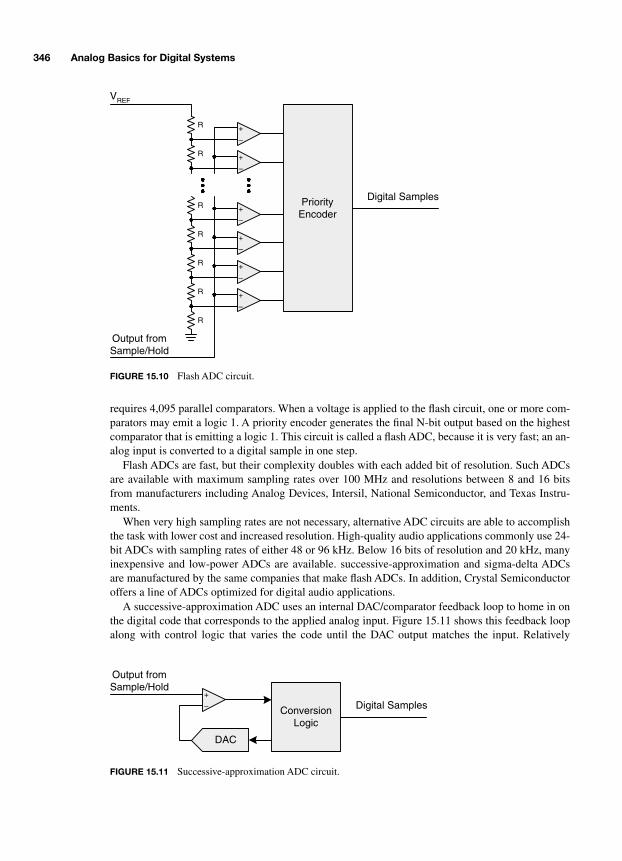
346 Analog Basics for Digital Systems
requires 4,095 parallel comparators. When a voltage is applied to the flash circuit, one or more com-parators may emit a logic 1. A priority encoder generates the final N-bit output based on the highestcomparator that is emitting a logic 1. This circuit is called a flash ADC, because it is very fast; an an-alog input is converted to a digital sample in one step.
Flash ADCs are fast, but their complexity doubles with each added bit of resolution. Such ADCsare available with maximum sampling rates over 100 MHz and resolutions between 8 and 16 bitsfrom manufacturers including Analog Devices, Intersil, National Semiconductor, and Texas Instru-ments.
When very high sampling rates are not necessary, alternative ADC circuits are able to accomplishthe task with lower cost and increased resolution. High-quality audio applications commonly use 24-bit ADCs with sampling rates of either 48 or 96 kHz. Below 16 bits of resolution and 20 kHz, manyinexpensive and low-power ADCs are available. successive-approximation and sigma-delta ADCsare manufactured by the same companies that make flash ADCs. In addition, Crystal Semiconductoroffers a line of ADCs optimized for digital audio applications.
A successive-approximation ADC uses an internal DAC/comparator feedback loop to home in onthe digital code that corresponds to the applied analog input. Figure 15.11 shows this feedback loopalong with control logic that varies the code until the DAC output matches the input. Relatively
PriorityEncoder
Digital Samples
Output fromSample/Hold
+
–
R
+
–
R
VREF
R
+
–
R
+
–
R
+
–
R
+
–
R
FIGURE 15.10 Flash ADC circuit.
ConversionLogic
Digital Samples
Output fromSample/Hold
+
–
DAC
FIGURE 15.11 Successive-approximation ADC circuit.
-Balch.book Page 346 Thursday, May 15, 2003 3:46 PM
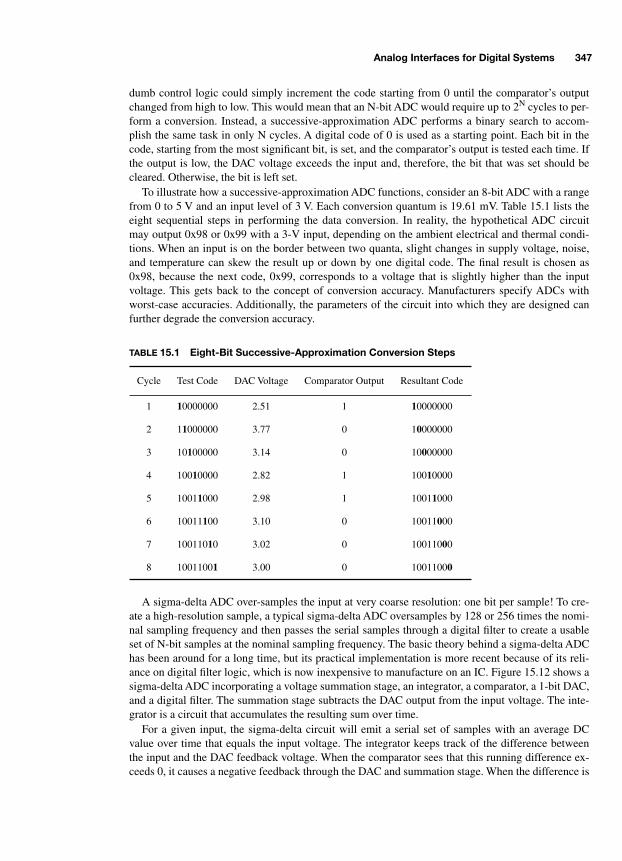
Analog Interfaces for Digital Systems 347
dumb control logic could simply increment the code starting from 0 until the comparator’s outputchanged from high to low. This would mean that an N-bit ADC would require up to 2
N
cycles to per-form a conversion. Instead, a successive-approximation ADC performs a binary search to accom-plish the same task in only N cycles. A digital code of 0 is used as a starting point. Each bit in thecode, starting from the most significant bit, is set, and the comparator’s output is tested each time. Ifthe output is low, the DAC voltage exceeds the input and, therefore, the bit that was set should becleared. Otherwise, the bit is left set.
To illustrate how a successive-approximation ADC functions, consider an 8-bit ADC with a rangefrom 0 to 5 V and an input level of 3 V. Each conversion quantum is 19.61 mV. Table 15.1 lists theeight sequential steps in performing the data conversion. In reality, the hypothetical ADC circuitmay output 0x98 or 0x99 with a 3-V input, depending on the ambient electrical and thermal condi-tions. When an input is on the border between two quanta, slight changes in supply voltage, noise,and temperature can skew the result up or down by one digital code. The final result is chosen as0x98, because the next code, 0x99, corresponds to a voltage that is slightly higher than the inputvoltage. This gets back to the concept of conversion accuracy. Manufacturers specify ADCs withworst-case accuracies. Additionally, the parameters of the circuit into which they are designed canfurther degrade the conversion accuracy.
A sigma-delta ADC over-samples the input at very coarse resolution: one bit per sample! To cre-ate a high-resolution sample, a typical sigma-delta ADC oversamples by 128 or 256 times the nomi-nal sampling frequency and then passes the serial samples through a digital filter to create a usableset of N-bit samples at the nominal sampling frequency. The basic theory behind a sigma-delta ADChas been around for a long time, but its practical implementation is more recent because of its reli-ance on digital filter logic, which is now inexpensive to manufacture on an IC. Figure 15.12 shows asigma-delta ADC incorporating a voltage summation stage, an integrator, a comparator, a 1-bit DAC,and a digital filter. The summation stage subtracts the DAC output from the input voltage. The inte-grator is a circuit that accumulates the resulting sum over time.
For a given input, the sigma-delta circuit will emit a serial set of samples with an average DCvalue over time that equals the input voltage. The integrator keeps track of the difference betweenthe input and the DAC feedback voltage. When the comparator sees that this running difference ex-ceeds 0, it causes a negative feedback through the DAC and summation stage. When the difference is
TABLE
15.1 Eight-Bit Successive-Approximation Conversion Steps
Cycle Test Code DAC Voltage Comparator Output Resultant Code
1
1
0000000 2.51 1
1
0000000
2 1
1
000000 3.77 0 1
0
000000
3 10
1
00000 3.14 0 10
0
00000
4 100
1
0000 2.82 1 100
1
0000
5 1001
1
000 2.98 1 1001
1
000
6 10011
1
00 3.10 0 10011
0
00
7 100110
1
0 3.02 0 100110
0
0
8 1001100
1
3.00 0 1001100
0
-Balch.book Page 347 Thursday, May 15, 2003 3:46 PM
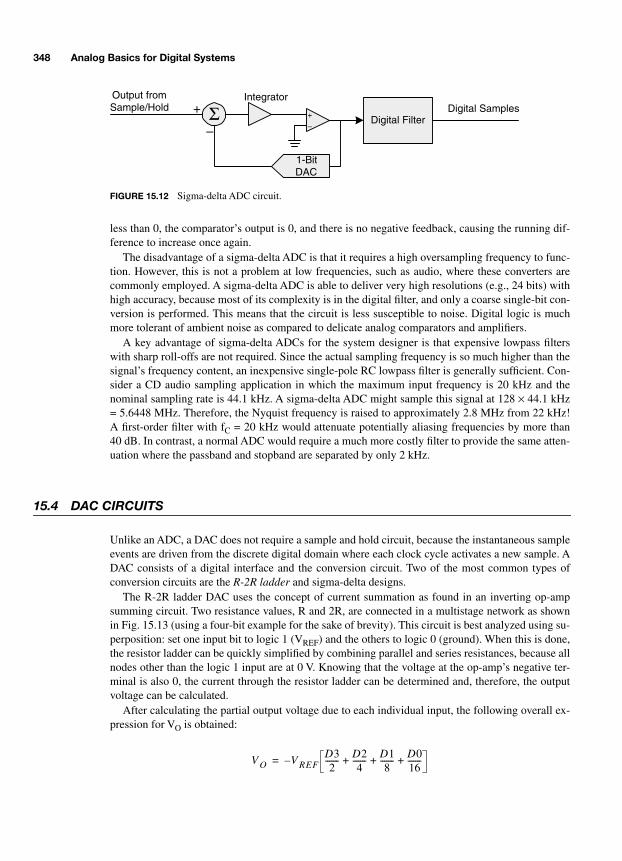
348 Analog Basics for Digital Systems
less than 0, the comparator’s output is 0, and there is no negative feedback, causing the running dif-ference to increase once again.
The disadvantage of a sigma-delta ADC is that it requires a high oversampling frequency to func-tion. However, this is not a problem at low frequencies, such as audio, where these converters arecommonly employed. A sigma-delta ADC is able to deliver very high resolutions (e.g., 24 bits) withhigh accuracy, because most of its complexity is in the digital filter, and only a coarse single-bit con-version is performed. This means that the circuit is less susceptible to noise. Digital logic is muchmore tolerant of ambient noise as compared to delicate analog comparators and amplifiers.
A key advantage of sigma-delta ADCs for the system designer is that expensive lowpass filterswith sharp roll-offs are not required. Since the actual sampling frequency is so much higher than thesignal’s frequency content, an inexpensive single-pole RC lowpass filter is generally sufficient. Con-sider a CD audio sampling application in which the maximum input frequency is 20 kHz and thenominal sampling rate is 44.1 kHz. A sigma-delta ADC might sample this signal at 128
×
44.1 kHz= 5.6448 MHz. Therefore, the Nyquist frequency is raised to approximately 2.8 MHz from 22 kHz!A first-order filter with f
C
= 20 kHz would attenuate potentially aliasing frequencies by more than40 dB. In contrast, a normal ADC would require a much more costly filter to provide the same atten-uation where the passband and stopband are separated by only 2 kHz.
15.4 DAC CIRCUITS
Unlike an ADC, a DAC does not require a sample and hold circuit, because the instantaneous sampleevents are driven from the discrete digital domain where each clock cycle activates a new sample. ADAC consists of a digital interface and the conversion circuit. Two of the most common types ofconversion circuits are the
R-2R ladder
and sigma-delta designs.The R-2R ladder DAC uses the concept of current summation as found in an inverting op-amp
summing circuit. Two resistance values, R and 2R, are connected in a multistage network as shownin Fig. 15.13 (using a four-bit example for the sake of brevity). This circuit is best analyzed using su-perposition: set one input bit to logic 1 (V
REF
) and the others to logic 0 (ground). When this is done,the resistor ladder can be quickly simplified by combining parallel and series resistances, because allnodes other than the logic 1 input are at 0 V. Knowing that the voltage at the op-amp’s negative ter-minal is also 0, the current through the resistor ladder can be determined and, therefore, the outputvoltage can be calculated.
After calculating the partial output voltage due to each individual input, the following overall ex-pression for V
O
is obtained:
Digital FilterDigital Samples
Output fromSample/Hold
+
–
1-BitDAC
Σ+
–
Integrator
FIGURE 15.12 Sigma-delta ADC circuit.
V O V REFD32
------- D24
------- D18
------- D016-------+ + +–=
-Balch.book Page 348 Thursday, May 15, 2003 3:46 PM
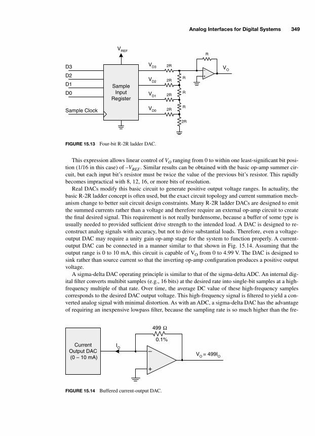
Analog Interfaces for Digital Systems 349
This expression allows linear control of
V
O
ranging from 0 to within one least-significant bit posi-tion (1/16 in this case) of –
V
REF
. Similar results can be obtained with the basic op-amp summer cir-cuit, but each input bit’s resistor must be twice the value of the previous bit’s resistor. This rapidlybecomes impractical with 8, 12, 16, or more bits of resolution.
Real DACs modify this basic circuit to generate positive output voltage ranges. In actuality, thebasic R-2R ladder concept is often used, but the exact circuit topology and current summation mech-anism change to better suit circuit design constraints. Many R-2R ladder DACs are designed to emitthe summed currents rather than a voltage and therefore require an external op-amp circuit to createthe final desired signal. This requirement is not really burdensome, because a buffer of some type isusually needed to provided sufficient drive strength to the intended load. A DAC is designed to re-construct analog signals with accuracy, but not to drive substantial loads. Therefore, even a voltage-output DAC may require a unity gain op-amp stage for the system to function properly. A current-output DAC can be connected in a manner similar to that shown in Fig. 15.14. Assuming that theoutput range is 0 to 10 mA, this circuit is capable of V
O
from 0 to 4.99 V. The DAC is designed tosink rather than source current so that the inverting op-amp configuration produces a positive outputvoltage.
A sigma-delta DAC operating principle is similar to that of the sigma-delta ADC. An internal dig-ital filter converts multibit samples (e.g., 16 bits) at the desired rate into single-bit samples at a high-frequency multiple of that rate. Over time, the average DC value of these high-frequency samplescorresponds to the desired DAC output voltage. This high-frequency signal is filtered to yield a con-verted analog signal with minimal distortion. As with an ADC, a sigma-delta DAC has the advantageof requiring an inexpensive lowpass filter, because the sampling rate is so much higher than the fre-
+
– VO
R
2R
2R
2R
VD3
VD2
VD1
VD0
R
SampleInput
Register
Sample Clock
VREF
D3
D2
D1
D0 R
2R
R
2R
FIGURE 15.13 Four-bit R-2R ladder DAC.
+
–
499 Ω
VO = 499IO
IO
0.1%Current
Output DAC(0 – 10 mA)
FIGURE 15.14 Buffered current-output DAC.
-Balch.book Page 349 Thursday, May 15, 2003 3:46 PM

350 Analog Basics for Digital Systems
quencies generated. These devices are commonly used in digital audio equipment because of theirlow overall system cost and high resolution (16 to 24 bits) for frequencies below 100 kHz.
15.5 FILTERS IN DATA CONVERSION SYSTEMS
General noise-reduction filters are typically found on the power supplies feeding data conversion cir-cuits, because less distortion of the analog signals results when there is less overall noise in the sys-tem. Purely digital systems are not immune to noise, but their tolerance threshold is much higherthan for analog systems because of their highly quantized binary signals. It takes noise of greatermagnitude to turn a 0 into a 1 than it does to distort a continuous analog signal.
In addition to general noise reduction, anti-aliasing filters are a key design aspect of data conver-sion systems. Filtering requirements dictated by the sampling rate and by the presence of undesiredfrequency content can be quite stringent. As the gap between the Nyquist frequency and the unde-sired frequencies decreases, more complex filters are necessary. The design of such complex filtersrequires a substantial set of analog design skills, the majority of which are outside the scope of thisbook. However, this chapter closes by identifying some of the issues that arise in anti-alias filteringso that you may be aware of them.
The first step in specifying an anti-aliasing filter is to identify how much attenuation is necessaryin the stopband. An ADC or DAC can resolve an analog signal only to a finite resolution given by thenumber of bits that are supported. It is therefore unnecessary to attenuate high-frequency content be-yond the point at which the circuit’s inherent capabilities reach their limit. Attenuating unwantedsignals to less than one-half of a voltage quantum renders them statistically insignificant. If a systemrepresents an analog signal with N bits of resolution, this minimum attenuation,
A
MIN
, is given as
One-half of a quantum is represented by the added power-of-two beyond that specified by the con-version resolution. The term represents an allowance for the average quantization noise magni-tude. As expected, a higher-resolution conversion requires greater attenuation, because thequantization noise is reduced. An 8-bit ADC, relatively low resolution by modern standards, requiresa stopband gain of –59 dB to prevent distortion due to aliasing. A 12-bit ADC, quite moderate in res-olution, requires attenuation of 83 dB.
Once the stopband gain is known, the filter’s roll-off target can be determined by identifying theseparation of the passband and stopband. Filter design is not a trivial process when minimal distor-tion is a design criterion. A real filter does not have perfectly uniform passband gain and thereforeadds some distortion by attenuating some frequencies more than others even in the passband. Whenthe passband and stopband are close together, a higher-order filter is called for to provide the neces-sary attenuation. Yet, filters with sharp roll-off can have the undesired side effect of exhibiting reso-nance around the cutoff frequency.
Additionally, filters do not simply change the amplitude of signals that pass through them butchange their phase as well by introducing a finite time delay or phase shift. The problem is that fil-ters do not have a uniform phase delay at all frequencies in the passband. Most real signals are notpure sine waves and therefore are composed of many frequencies. The result is distortion of theoverall signal as the different frequency components are shifted relative to each other by slightly dif-ferent delays.
The magnitude of these nonideal filter characteristics depends on each situation. A basic first-or-der RC filter is very well behaved, which is a key reason why sigma-delta conversion circuits are so
AMIN 20 2N 1+
3( )log–=
3
-Balch.book Page 350 Thursday, May 15, 2003 3:46 PM

Analog Interfaces for Digital Systems 351
popular. The limitation, of course, is that sigma-delta circuits can be used only at lower samplingrates.
If a sigma-delta circuit cannot be used for one reason or another, it may be practical to operate aconventional ADC or DAC at a significantly higher sampling rate than would be dictated by the fre-quency of interest. This allows a less complex filter to be used by increasing the separation betweenthe signal and Nyquist frequencies. Digital signal processing techniques can then be used to filter thedigital samples down to a more ideal sampling rate. The difference here is that the complexity of an-alog filter design is traded off against a faster data conversion system and some computational num-ber crunching. As logic gates have become inexpensive and microprocessors increase in capability,DSP-based filter algorithms are often far superior to their analog implementations, because the non-ideal characteristics of phase-delay, amplitude variance, and resonance are overcome by arithmeticmanipulations. A major reason behind the proliferation of high-speed ADC and DAC ICs is theemergence of DSP technology in applications in which fully analog circuits formerly existed. DSPalgorithms can implement complex and highly stable filters that are extremely costly to implementwith analog components.
-Balch.book Page 351 Thursday, May 15, 2003 3:46 PM

This page intentionally left blank.

P R TA 4
DIGITAL SYSTEM DESIGN IN PRACTICE
-Balch.book Page 353 Thursday, May 15, 2003 3:46 PM
Copyright 2003 by The McGraw-Hill Companies, Inc. Click Here for Terms of Use.

This page intentionally left blank.
355
CHAPTER 16
Clock Distribution
Clocks are inherently critical pieces of a digital system. Reliable operation requires the distributionof electrically clean, well timed clocks to all synchronous components in the system. Clocking prob-lems are one of the last bugs that an engineer wants to have in a system, because everything else isbuilt on the assumption of nearly ideal clocks. This chapter concentrates on the means of distributinglow-skew and low-jitter clocks in a system. Most systems require the design of a
clock tree—
a cir-cuit that uses an oscillator of some type to create a clock and then distributes that clock to multipleloads, akin to branches in a tree. Simple clock trees may have a single level of hierarchy in which theoscillator directly drives a few loads. More complex trees have several levels of buffers and othercomponents when tens of loads are present.
Basic information on crystal oscillators is presented first to assist in the selection of a suitabletime base from which to begin a clock tree. Once a master clock has been produced, low-skew buff-ers are the common means of replicating that clock to several loads. These buffers are explained withexamples incorporating length matching for low-skew and termination resistors for signal integrity.Buffers are followed up with a discussion of phase-locked loops, commonly used to implement“zero-delay” buffers in clock trees. These devices become important when a system contains multi-ple boards and when there are special clocking sources other than a stand-alone oscillator. Low-skewand zero-delay buffers form the basis for most clock tree designs.
The second portion of the chapter discusses more advanced clocking concepts beginning with fre-quency synthesis. Originally conceived for analog and RF applications, frequency synthesis is animportant part of many high-performance digital systems. It allows multiple clocks to be derivedfrom a single time base and is how a leading-edge microprocessor operates many times faster inter-nally than it does externally. Frequency synthesis can also be important when processing data be-tween multiple interfaces that run at different frequencies.
Next, delay-locked loop technology is presented, because it can accomplish the same basic func-tion as a phase-locked loop in many cases but is a purely digital circuit with resultant implementa-tion advantages. The chapter concludes with a brief discussion of source-synchronous interfaces as anecessary alternative to conventional synchronous design when dealing with very high frequencies.
16.1 CRYSTAL OSCILLATORS AND CERAMIC RESONATORS
An electronic clock consists of an amplifier with a passive time-base element coupled into its feed-back loop. It has previously been shown that a simple oscillator can be formed with just an RC timebase and an inverter that serves as an amplifier. Simpler yet is connecting the output of the inverterdirectly to its input via a piece of wire sized to provide a certain time delay. While simple, neither ofthese approaches yields a sufficiently accurate clock source in most applications. Accurate time-
-Balch.book Page 355 Thursday, May 15, 2003 3:46 PM
Copyright 2003 by The McGraw-Hill Companies, Inc. Click Here for Terms of Use.
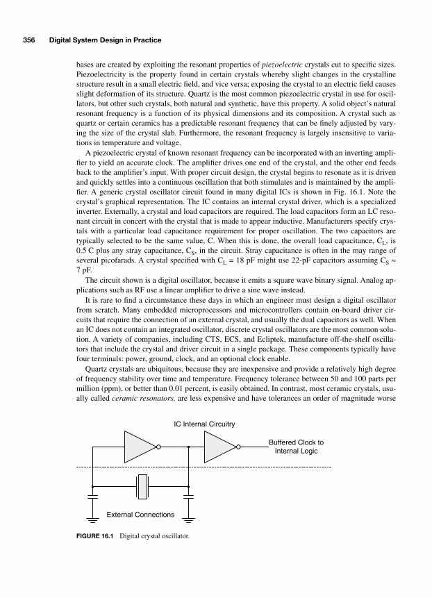
356 Digital System Design in Practice
bases are created by exploiting the resonant properties of
piezoelectric
crystals cut to specific sizes.Piezoelectricity is the property found in certain crystals whereby slight changes in the crystallinestructure result in a small electric field, and vice versa; exposing the crystal to an electric field causesslight deformation of its structure. Quartz is the most common piezoelectric crystal in use for oscil-lators, but other such crystals, both natural and synthetic, have this property. A solid object’s naturalresonant frequency is a function of its physical dimensions and its composition. A crystal such asquartz or certain ceramics has a predictable resonant frequency that can be finely adjusted by vary-ing the size of the crystal slab. Furthermore, the resonant frequency is largely insensitive to varia-tions in temperature and voltage.
A piezoelectric crystal of known resonant frequency can be incorporated with an inverting ampli-fier to yield an accurate clock. The amplifier drives one end of the crystal, and the other end feedsback to the amplifier’s input. With proper circuit design, the crystal begins to resonate as it is drivenand quickly settles into a continuous oscillation that both stimulates and is maintained by the ampli-fier. A generic crystal oscillator circuit found in many digital ICs is shown in Fig. 16.1. Note thecrystal’s graphical representation. The IC contains an internal crystal driver, which is a specializedinverter. Externally, a crystal and load capacitors are required. The load capacitors form an LC reso-nant circuit in concert with the crystal that is made to appear inductive. Manufacturers specify crys-tals with a particular load capacitance requirement for proper oscillation. The two capacitors aretypically selected to be the same value, C. When this is done, the overall load capacitance, C
L
, is0.5 C plus any stray capacitance, C
S
, in the circuit. Stray capacitance is often in the may range ofseveral picofarads. A crystal specified with C
L
= 18 pF might use 22-pF capacitors assuming C
S
≈
7 pF.The circuit shown is a digital oscillator, because it emits a square wave binary signal. Analog ap-
plications such as RF use a linear amplifier to drive a sine wave instead.It is rare to find a circumstance these days in which an engineer must design a digital oscillator
from scratch. Many embedded microprocessors and microcontrollers contain on-board driver cir-cuits that require the connection of an external crystal, and usually the dual capacitors as well. Whenan IC does not contain an integrated oscillator, discrete crystal oscillators are the most common solu-tion. A variety of companies, including CTS, ECS, and Ecliptek, manufacture off-the-shelf oscilla-tors that include the crystal and driver circuit in a single package. These components typically havefour terminals: power, ground, clock, and an optional clock enable.
Quartz crystals are ubiquitous, because they are inexpensive and provide a relatively high degreeof frequency stability over time and temperature. Frequency tolerance between 50 and 100 parts permillion (ppm), or better than 0.01 percent, is easily obtained. In contrast, most ceramic crystals, usu-ally called
ceramic resonators,
are less expensive and have tolerances an order of magnitude worse
External Connections
IC Internal Circuitry
Buffered Clock toInternal Logic
FIGURE 16.1 Digital crystal oscillator.
-Balch.book Page 356 Thursday, May 15, 2003 3:46 PM

Clock Distribution 357
than common quartz crystals. Ceramic resonators are used in very low-cost applications wherein ac-curacy is forsaken for small cost savings. Most digital systems use quartz crystals that cost approxi-mately $1.00, because they are reliable, they provide an accurate time base, and the crystal’s cost isa small fraction of the overall system cost.
Some applications require tighter tolerances than normal crystal oscillators provide. More precisemanufacturing techniques and control over materials can yield tolerances of approximately 1 ppm.Below this level, temperature control becomes a significant factor in frequency stability. So-called
oven-controlled oscillators
are specially designed to maintain the crystal at a stable temperature togreatly reduce temperature as a variable in the crystal’s resonant frequency. Using this technique, os-cillators are available with tolerances on the order of one part per billion! Conner-Winfield and Vec-tron International, among others, manufacture these high-accuracy oscillator products.
Most digital systems do not require clock accuracy better than 50 or 100 ppm. However, jitter isanother clock stability characteristic of concern. Each oscillator circuit is subject to a certain amountof jitter based on the tolerance of its components. Aside from an oscillator’s inherent jitter specifica-tion, ambient noise can couple into the oscillator and cause additional jitter. Therefore, it is desirableto attenuate ambient noise on the power supply that might otherwise couple into the oscillator cir-cuit. It is common to find various types of LC filters on the power leads of crystal oscillators. A basicpi-type topology is shown in Fig. 16.2, consisting of a ferrite bead with capacitors on each side to at-tenuate high frequencies with small capacitors and provide lower frequency response with a largercapacitor. This circuit attenuates differential noise and provides the oscillator with a cleaner powersupply relative to its ground reference.
16.2 LOW-SKEW CLOCK BUFFERS
Once a stable clock source has been established, the signal must be distributed to all componentsthat operate on that clock. Clock distribution is critical to a digital system, because synchronous tim-ing analysis assumes the presence of a reliable and consistent clock. Conventional synchronousbuses running between ICs require a common clock so that they can work together with a knowntiming relationship. A single bit on a synchronous bus essentially consists of an output flop on oneIC that drives an external wire, possibly passes through some combinatorial logic, and then is sam-pled at the input of a flop on another IC. Each IC on the bus should ideally see the same clock signal.In reality, there are slight skew variations between these individual clocks. Some clocks arrive a littlesooner than others. Skew should be kept to a minimum because, like jitter, it reduces the synchro-nous timing budget.
Common clock signals are distributed in a low-skew manner by closely matching the delays fromthe clock source to all loads. Distribution delays are incurred as the clock passes through passivewires and active buffers. Consider the hypothetical clock distribution tree shown in Fig. 16.3. An os-cillator drives a clock buffer, which drives five loads. All of the clock signals are point-to-point with
Ferrite BeadVIN
0.1 µF 0.1 µF 10 µF
VFILTEREDOscillator
FIGURE 16.2 Oscillator LC pi power filter.
-Balch.book Page 357 Thursday, May 15, 2003 3:46 PM

358 Digital System Design in Practice
a single driver and a single load. It is assumed that each load is approximately the same as all otherloads, which is usually the case when dealing with ICs. If one load is dramatically different from theothers, it may cause its respective driver in the clock buffer to behave differently, and this couldhinder the goal of creating a tree with balanced delays.
The absolute propagation delay from the oscillator to each load is immaterial in this case, becauseall that matters is that each load sees a clock with the same timing as the others. Therefore, the vari-ables of interest are those that can potentially cause differential delays, or skew. The first such vari-able is the propagation delay variation from the buffer input to each output. Each output driver in anIC has slightly different physical properties that cause its propagation delay to vary within a narrowrange. Low-skew clock buffers are specifically designed to minimize this variation. The acceptableamount of skew varies by application but generally declines with increasing frequency and with theuse of faster devices, even at lower frequencies. Older low-skew buffers with pin-to-pin skews ofbetter than 1 ns are still available for systems running at moderate frequencies. Newer buffers withskews of 200 to 50 ps are available for systems with very low skew budgets. Manufacturers of thesebuffers include Cypress Semiconductor, Integrated Circuit Systems, Integrated Device Technolo-gies, and Texas Instruments. The second skew variable in this example is the variation in wirelengths connecting the buffer to each load. Wire delays are matched by matching wire lengths.Matching clock trace lengths when designing a PCB is one of the basics of proper clock distribution.
Signal integrity is tightly coupled with clock distribution concepts, because electrically cleanclocks are a prerequisite for a digital system’s reliable operation. Flops can be falsely triggered bynonmonotonic edges resulting from clocks that are improperly distributed in a way that causes theiredges to become significantly distorted. Signal integrity is the topic of a later chapter, but a few ba-sics are introduced here because of their relevance. The goal when distributing a clock is to preventreflections on the transmission line that are formed by the wires that carry that clock signal. Reflec-tions can result when a signal transitions rapidly relative to its propagation delay across the transmis-sion line. It rises or falls so rapidly that one end of the wire is at a different voltage from the otherend. Reflections distort a signal, because the instantaneous voltage on a wire is the sum of the drivensignal and any reflected voltages that are present. A reflection occurs when a signal travels across animpedance discontinuity. Some energy passes through the discontinuity, and some is reflected backto its source. Terminating a transmission line with its characteristic impedance prevents reflectionsfrom occurring, because no impedance discontinuity exists.
One easy way of terminating a point-to-point wire that is always driven from one end is with
source termination
, also called
series termination
. This technique is illustrated in Fig. 16.4 as an en-hancement to the single-buffer clock tree example. A resistor is placed at the driver and is sized suchthat its resistance plus that of the driver, Z
D
, is approximately equal to the transmission line’s charac-teristic impedance, Z
O
. For this example, it is assumed that a transmission line with Z
O
= 50
Ω
is im-plemented on a PCB and that the clock buffer’s driver has Z
D
≈
10
Ω
. Therefore, the series resistors
50 MHzOscillator
Load #1
Load #2
Load #3
Load #4
Load #5
Matched Length
Clock Buffer
FIGURE 16.3 Single-buffer clock tree.
-Balch.book Page 358 Thursday, May 15, 2003 3:46 PM
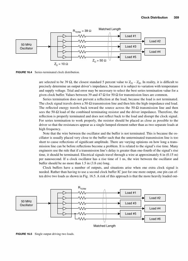
Clock Distribution 359
are selected to be 39
Ω
, the closest standard 5 percent value to Z
O
– Z
D
. In reality, it is difficult toprecisely determine an output driver’s impedance, because it is subject to variation with temperatureand supply voltage. Trial and error may be necessary to select the best series termination value for agiven clock buffer. Values between 39 and 47
Ω
for 50
Ω
for transmission lines are common.Series termination does not prevent a reflection at the load, because the load is not terminated.
The clock signal travels down a 50-
Ω
transmission line and then hits the high-impedance end load.The reflected energy travels back toward the source across the 50-
Ω
transmission line and thensees the 50-
Ω
load of the combined terminating resistor and the driver impedance. Therefore, thereflection is properly terminated and does not reflect back to the load and disrupt the clock signal.For series termination to work properly, the resistor should be placed as close as possible to thedriver so that the resistances appear as a single lumped element rather than as two separate loads athigh frequency.
Note that the wire between the oscillator and the buffer is not terminated. This is because the os-cillator is usually placed very close to the buffer such that the unterminated transmission line is tooshort to cause reflections of significant amplitude. There are varying opinions on how long a trans-mission line can be before reflections become a problem. It is related to the signal’s rise time. Manyengineers use the rule that if a transmission line’s delay is greater than one-fourth of the signal’s risetime, it should be terminated. Electrical signals travel through a wire at approximately 6 in (0.15 m)per nanosecond. If a clock oscillator has a rise time of 1 ns, the wire between the oscillator andbuffer should be no more than 1.5 in (3.8 cm) long.
Clock buffers have a number of outputs, and situations arise when one extra clock signal isneeded. Rather than having to use a second clock buffer IC just for one more output, one pin can of-ten drive two loads as shown in Fig. 16.5. A risk of this approach is that the more heavily loaded out-
RTERM = 39 Ω
50 MHzOscillator
Load #1
Load #2
Load #3
Load #4
Load #5ZO = 50 Ω
ZD = 10 Ω
Matched Length
FIGURE 16.4 Series-terminated clock distribution.
RTERM
50 MHzOscillator
Load #1
Load #2
Load #3
Load #4
Load #5
Matched Length
Load #6
FIGURE 16.5 Single output driving two loads.
-Balch.book Page 359 Thursday, May 15, 2003 3:46 PM

360 Digital System Design in Practice
put will cause unacceptable skew to develop with respect to the other pins that are driving only asingle load. Whether this occurs depends on each situation’s skew tolerance, clock buffer drivestrength, and input impedance of the clock load.
As the number of clock loads in a system increases, there comes a point at which clock distribu-tion cannot be performed using a single clock buffer IC. Using multiple clock buffers introduces anew source of skew: part-to-part propagation delay variation. It is easier to manage skew on a singlechip, because each output circuit has very similar physical properties to its neighbors, and the tem-perature variation across a small chip is very low. Neither of these assumptions automatically holdstrue when dealing with separate ICs. Some low-skew clock buffers are specially designed and fabri-cated for low part-to-part skew specifications. Newer devices are available with part-to-part skews of0.5 ns, and more mature devices with 1 ns part-to-part skews are available as well. Figure 16.6shows how two clock buffers might be connected to drive twice the number of loads as shown previ-ously. Note that the oscillator directly drives both buffers in parallel without any termination, be-cause it is assumed that the wire length is short enough to minimize reflections. If more than acouple of buffers are necessary to distribute clocks to the system, an intermediate buffer shouldprobably be placed between the oscillator and final buffers so that the oscillator does not have todrive too many loads.
16.3 ZERO-DELAY BUFFERS: THE PLL
Low-skew buffers do an excellent job of distributing clocks with minimal relative delays when thereis no constraint on the absolute propagation delay from the clock tree input to its outputs. However,there are circumstances where the absolute delay is as important as the relative delay. Many micro-processors with synchronous bus interfaces generate their own bus clock internally and emit thisclock on an output pin. All bus signals must be timed relative to that output clock to meet the micro-processor’s timing rules of t
CO
, t
SU
, and t
H
. If the microprocessor communicates with just one pe-
50 MHzOscillator
Load #6
Load #7
Load #8
Load #9
Load #10
RTERM
Load #1
Load #2
Load #3
Load #4
Load #5
Matched Length
Load #3
Buffer #1
Buffer #2
FIGURE 16.6 Dual-buffer clock tree.
-Balch.book Page 360 Thursday, May 15, 2003 3:46 PM
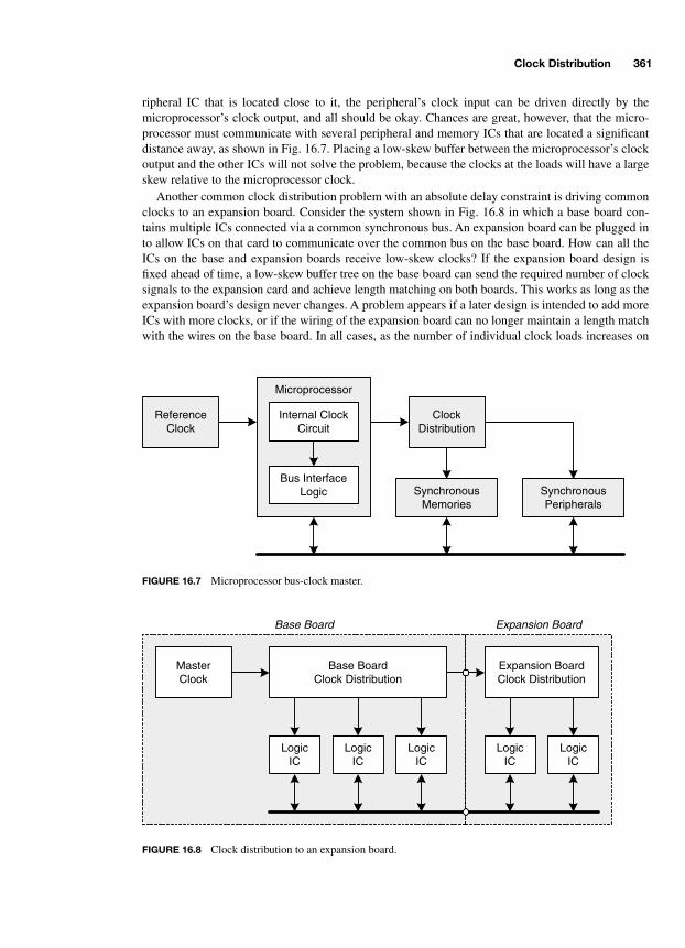
Clock Distribution 361
ripheral IC that is located close to it, the peripheral’s clock input can be driven directly by themicroprocessor’s clock output, and all should be okay. Chances are great, however, that the micro-processor must communicate with several peripheral and memory ICs that are located a significantdistance away, as shown in Fig. 16.7. Placing a low-skew buffer between the microprocessor’s clockoutput and the other ICs will not solve the problem, because the clocks at the loads will have a largeskew relative to the microprocessor clock.
Another common clock distribution problem with an absolute delay constraint is driving commonclocks to an expansion board. Consider the system shown in Fig. 16.8 in which a base board con-tains multiple ICs connected via a common synchronous bus. An expansion board can be plugged into allow ICs on that card to communicate over the common bus on the base board. How can all theICs on the base and expansion boards receive low-skew clocks? If the expansion board design isfixed ahead of time, a low-skew buffer tree on the base board can send the required number of clocksignals to the expansion card and achieve length matching on both boards. This works as long as theexpansion board’s design never changes. A problem appears if a later design is intended to add moreICs with more clocks, or if the wiring of the expansion board can no longer maintain a length matchwith the wires on the base board. In all cases, as the number of individual clock loads increases on
ReferenceClock
Microprocessor
Internal ClockCircuit
Bus InterfaceLogic Synchronous
MemoriesSynchronousPeripherals
ClockDistribution
FIGURE 16.7 Microprocessor bus-clock master.
MasterClock
LogicIC
Base BoardClock Distribution
LogicIC
LogicIC
Expansion BoardClock Distribution
LogicIC
LogicIC
Base Board Expansion Board
FIGURE 16.8 Clock distribution to an expansion board.
-Balch.book Page 361 Thursday, May 15, 2003 3:46 PM

362 Digital System Design in Practice
the expansion board, more pins or wires must be used to make the required connections. The in-creased connectivity increases cost yet does not improve the design’s flexibility and tolerance of fu-ture changes.
A clock’s purpose in a system is to provide a regular timing reference. Clock signals do not commu-nicate information, because they are repetitive, and no single clock cycle has unique properties to set itapart from others. Therefore, a clock can be arbitrarily delayed without losing or gaining information.As with sine waves, periodic signals complete one full cycle over 360°. If a clock is delayed by an in-teger multiple of 360°, its delay cannot be detected, because each cycle is identical to all others, and itstransition edges still occur at the same relative points in time. This important principle enables solu-tions to the clock distribution problems just posed and others like them. While it is physically impossi-ble to construct a clock distribution circuit with zero delay, the end result of zero delay can bereplicated by purposely adding more delay until an integer multiple of a 360° delay has been achieved.
Without a special trick, it would be extremely difficult to adjust a circuit for a perfect 360xN-de-gree delay. Propagation delays through semiconductors and wires have too much variation for this tobe practical. The secret to achieving near perfect delays is with a closed-loop control system knownas a
phase-locked loop
, or PLL. A PLL continually monitors a feedback clock signal and compares itagainst a reference clock to determine phase, or delay, errors. As soon as a phase shift is detected,the PLL can respond and compensate for that delay. This continuous compensation makes a PLL ex-ceptionally able to deal with varying delays due to time, temperature, and voltage. PLLs are analogcircuits and were originally invented for use in radio modulators and receivers. FM radios, televi-sions, and cellular telephones would not be possible without PLLs.
Figure 16.9 shows the structure of a generic PLL. A PLL is built around a
voltage controlled os-cillator
, or VCO. The oscillating frequency of a VCO is proportional to its analog control voltage in-put. A phase detector drives the VCO’s control input through a lowpass filter. When the referenceand feedback clock edges occur at the same time, the input and output clocks are aligned by 360xNdegrees, and the phase detector emits a neutral error signal, enabling the VCO to maintain its fre-quency. If the VCO begins to wander, as all oscillators do to a certain extent, the feedback clockedges begin to shift relative to the reference. As soon as this happens, the phase detector generates anerror signal, which causes the VCO to slightly increase or decrease its frequency to move the feed-back clock edge back into phase with the reference. One of the beauties of a PLL is that it can use aninexpensive VCO, because the feedback loop keeps the VCO at the correct frequency. A phase detec-tor responds very quickly to phase errors, and the potential exists for an unstable control system re-sulting from rapid overcompensation. The lowpass filter stabilizes the control and feedback loop toaverage the phase detector output so that the VCO sees a more gradual control slew as compared torapid swings.
PLLs are analog circuits and their design is a non-trivial task. Fortunately, numerous companiesmanufacture special-purpose digital PLLs that are designed for clock distribution applications. All
VCO Clock BufferLowpassLoop FilterPhase Detector
Reference (Input)Clock
Feedback Clock
FIGURE 16.9 Generic phase-locked loop.
-Balch.book Page 362 Thursday, May 15, 2003 3:46 PM
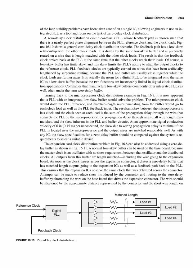
Clock Distribution 363
of the loop stability problems have been taken care of on a single IC, allowing engineers to use an in-tegrated PLL as a tool and focus on the task of zero-delay clock distribution.
A zero-delay clock distribution circuit contains a PLL whose feedback path is chosen such thatthere is a nearly perfect phase alignment between the PLL reference clock and the clock loads. Fig-ure 16.10 shows a general zero-delay clock distribution scenario. The feedback path has a low-skewrelationship with the other clock loads. It is driven by the same low-skew buffer and is purposelyrouted on a wire that is length matched with the other clock loads. The result is that the feedbackclock arrives back at the PLL at the same time that the other clocks reach their loads. Of course, alow-skew buffer has finite skew, and this skew limits the PLL’s ability to align the output clocks tothe reference clock. PLL feedback clocks are typically carried on wires that have been artificiallylengthened by serpentine routing, because the PLL and buffer are usually close together while theclock loads are further away. It is actually the norm for a digital PLL to be integrated onto the sameIC as a low-skew buffer, because the two functions are inextricably linked in digital clock distribu-tion applications. Companies that manufacture low-skew buffers commonly offer integrated PLLs aswell, often under the term
zero-delay buffer
.Turning back to the microprocessor clock distribution example in Fig. 16.7, it is now apparent
that a PLL with an integrated low-skew buffer would solve the problem. The microprocessor clockwould drive the PLL reference, and matched-length wires emanating from the buffer would go toeach clock load as well as the PLL feedback input. The resultant skew between the microprocessor’sbus clock and the clock seen at each load is the sum of the propagation delay through the wire thatconnects the PLL to the microprocessor, the propagation delay through any small wire length mis-matches, and the skew inherent in the PLL and buffer circuits. At an approximate signal conductionvelocity of 6 in (0.15 m) per nanosecond, the skew due to wiring propagation delay is minimal if thePLL is located near the microprocessor and the output wires are matched reasonably well. As withany IC, the skew specifications for a zero-delay buffer should be compared against the system’s re-quirements to select a suitable device.
The expansion card clock distribution problem in Fig. 16.8 can also be addressed using a zero-de-lay buffer as shown in Fig. 16.11. A normal low-skew buffer can be used on the base board, becausethe master clock is an oscillator with no skew requirement between that oscillator and the distributedclocks. All outputs from this buffer are length matched—including the wire going to the expansionboard. As soon as the clock passes across the expansion connector, it drives a zero-delay buffer thathas matched length outputs going to the expansion ICs as well as a feedback path back to the PLL.This ensures that the expansion ICs observe the same clock that was delivered across the connector.Attempts can be made to reduce skew introduced by the connector and routing to the zero-delaybuffer by shortening the wire on the base board that drives the expansion connector. The wire shouldbe shortened by the approximate distance represented by the connector and the short wire length on
Load #1
Load #2
Load #3
Load #4
Matched Length
Reference Clock
DigitalPLL
Feedback Clock
FIGURE 16.10 Zero-delay clock distribution.
-Balch.book Page 363 Thursday, May 15, 2003 3:46 PM
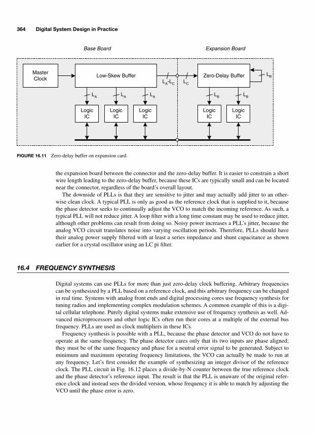
364 Digital System Design in Practice
the expansion board between the connector and the zero-delay buffer. It is easier to constrain a shortwire length leading to the zero-delay buffer, because these ICs are typically small and can be locatednear the connector, regardless of the board’s overall layout.
The downside of PLLs is that they are sensitive to jitter and may actually add jitter to an other-wise clean clock. A typical PLL is only as good as the reference clock that is supplied to it, becausethe phase detector seeks to continually adjust the VCO to match the incoming reference. As such, atypical PLL will not reduce jitter. A loop filter with a long time constant may be used to reduce jitter,although other problems can result from doing so. Noisy power increases a PLL’s jitter, because theanalog VCO circuit translates noise into varying oscillation periods. Therefore, PLLs should havetheir analog power supply filtered with at least a series impedance and shunt capacitance as shownearlier for a crystal oscillator using an LC pi filter.
16.4 FREQUENCY SYNTHESIS
Digital systems can use PLLs for more than just zero-delay clock buffering. Arbitrary frequenciescan be synthesized by a PLL based on a reference clock, and this arbitrary frequency can be changedin real time. Systems with analog front ends and digital processing cores use frequency synthesis fortuning radios and implementing complex modulation schemes. A common example of this is a digi-tal cellular telephone. Purely digital systems make extensive use of frequency synthesis as well. Ad-vanced microprocessors and other logic ICs often run their cores at a multiple of the external busfrequency. PLLs are used as clock multipliers in these ICs.
Frequency synthesis is possible with a PLL, because the phase detector and VCO do not have tooperate at the same frequency. The phase detector cares only that its two inputs are phase aligned;they must be of the same frequency and phase for a neutral error signal to be generated. Subject tominimum and maximum operating frequency limitations, the VCO can actually be made to run atany frequency. Let’s first consider the example of synthesizing an integer divisor of the referenceclock. The PLL circuit in Fig. 16.12 places a divide-by-N counter between the true reference clockand the phase detector’s reference input. The result is that the PLL is unaware of the original refer-ence clock and instead sees the divided version, whose frequency it is able to match by adjusting theVCO until the phase error is zero.
MasterClock
LogicIC
Low-Skew Buffer
LogicIC
LogicIC
Zero-Delay Buffer
LogicIC
LogicIC
Base Board Expansion Board
LA LA LA LB LB
LB
LA-LC LC
FIGURE 16.11 Zero-delay buffer on expansion card.
-Balch.book Page 364 Thursday, May 15, 2003 3:46 PM

Clock Distribution 365
Clock division by an integer divisor is not very interesting, because it can be done without thecomplexity of a PLL. Now let’s look at integer multiplication, which does require a PLL. The circuitin Fig. 16.13 places a divide-by-M counter in the feedback path between the VCO output and thephase detector. Things start to get interesting here. Instead of observing the true VCO signal, thephase detector unknowingly gets a divided version of that clock. The phase detector has no knowl-edge of what signals it is seeing—just whether they are phase aligned. Therefore, the phase detectoremits an error signal until the divided feedback clock matches the frequency and phase of the refer-ence. The VCO must run at a multiple of M times the reference for the feedback clock to equal thereference, resulting in clock multiplication.
Integer multipliers and dividers are useful, but truly arbitrary ratios between input and output canbe achieved when the reference and feedback dividers are joined into a single circuit. The circuit inFig. 16.14 allows the output to run at a ratio of M
÷
N times the reference frequency by combiningthe principles of the aforementioned divider and multiplier schemes. Different frequencies can besynthesized in real time by periodically changing the M and N counters. A PLL has a finite lock time,the time that the loop takes to adjust to a new operating frequency. Any frequency synthesis schemethat requires real-time adjustment must take the lock time into account. If the counters are changedtoo rapidly, the PLL may spend all of its time hunting for the new frequency and never settling.
PLLs in general are capable of frequency synthesis when complemented with external counters,but most digital PLLs are not designed specifically for large multiplication ratios. Several factors in-
Reference Clock Divide by NCounter
FIGURE 16.12 PLL clock divider.
Reference Clock
Divide-by-MCounter
FIGURE 16.13 PLL clock multiplier.
Reference Clock
Divide by MCounter
Divide by NCounter
FIGURE 16.14 PLL clock synthesizer.
-Balch.book Page 365 Thursday, May 15, 2003 3:46 PM

366 Digital System Design in Practice
fluence the suitability of a PLL for arbitrary clock synthesis, including VCO stability and loop-filtercharacteristics. VCO stability is improved by filtering its power supply. Typical core clock synthesisapplications in a microprocessor or logic IC may require multiplication by 2 or 4, which is relativelystraightforward. As the multiplication ratio increases, the control path between the phase detectorand the VCO is degraded, because fewer feedback adjustment opportunities exist for every VCOclock period. If a PLL is multiplying a reference by 100, the phase detector will only be able tojudge phase errors on 1 percent of the VCO edges. There is the potential for VCO wander during thelong intervals between phase detector corrections.
Most digital PLLs contain a lowpass loop filter integrated on chip that is matched to the typicaloperating scenario of a 1:1 input/output ratio or some small multiplication factor. Larger multipli-cation ratios may require a more complex off-chip filter that is specifically designed for the appli-cation’s requirements. This is where PLL design in a digital system can start to get complicated.Fortunately, semiconductor manufacturers have documentation and applications engineering staffavailable to assist with such tasks. One set of devices that are well suited for digital frequencysynthesis is Texas Instruments’ TLC29xx family. The TLC29xx devices have separately con-nected phase detector and VCO sections such that an external loop-filter can be customized to theapplication.
It is not very common for a digital system to require complex multiplication ratios in a PLL, butthe requirement does exist in applications that have multiple interfaces that run at different fre-quencies and must be phase locked to prevent data loss. One example is a digital video processor.The primary clock frequency of many digital video standards is 27 MHz; however, some newerhigh-definition video standards operate at 74.25 MHz. These frequencies are related by a factor of2.75. If a digital video processor must perform some conversion between these two interfaces anddo so in a manner that precisely matches their data rates, a PLL is necessary to lock one of the in-terfaces to the other. Otherwise, each interface would run on its own oscillator, and small amountsof frequency drift would soon cause one to get a little faster or slower than the other. No matterhow accurate an oscillator is, it has a finite deviation from its nominal frequency. When two oscil-lators are paired with the expectation that they run at constant rates, a problem will eventually de-velop. As soon as a rate mismatch develops, the input and output data rates no longer match, anddata is corrupted.
For the sake of discussion, assume that the 27-MHz interface is the master, and the 74.25-MHzinterface is the slave. Because a counter cannot directly divide by 2.75, a ratio of integers must becalculated. The smallest pair of integers that yields M
÷
N = 2.75 is M = 11 and N = 4. This meansthat the PLL is essentially performing an 11
×
clock multiplication function, because the 27 MHz ref-erence is divided by 4 to yield a 6.75-MHz PLL input.
The task of designing a PLL to implement large multiplication factors is decidedly non-trivial be-cause of the problems of stability and jitter. Selecting an appropriate lowpass filter that keeps theloop from unstable oscillations and that adequately addresses VCO jitter can involve significant con-trol systems theory and analog filter design skills.
16.5 DELAY-LOCKED LOOPS
PLLs have traditionally been considered the standard mechanism for implementing zero-delay buff-ering and clock multiplication. Their flexibility comes at a certain price for manufacturers of digitalICs, because PLLs are analog circuits that must be isolated from noisy digital switching power sup-plies for low-jitter operation. Although the problems of on-chip isolation have been addressed for along time, the problem persists. Many large digital ICs are now manufactured with a purely digital
-Balch.book Page 366 Thursday, May 15, 2003 3:46 PM

Clock Distribution 367
delay-locked loop
, or DLL, that produces similar results to a PLL. Instead of controlling a VCO tovary the phase of the output clock, a DLL contains a many-tap digital delay line through which thereference clock propagates. According to the detected phase difference between the reference andfeedback clocks, a specific propagation delay can be picked in real time to align the edges. A DLLmay reduce problems in certain designs as a result of the reduced noise sensitivity of purely digitalcircuits and the lack of a VCO. Figure 16.15 shows a basic digital DLL where the delay is pro-grammed by selecting one of many delay line taps with a multiplexer. DLLs can also be designed asanalog circuits by employing a voltage controlled delay line. However, the purely digital implemen-tation is preferable due to its improved noise immunity.
A DLL must have sufficient delay granularity at each tap to be effective in minimizing skew be-tween its input and output. If the incremental delay is 100 ps, the DLL can offer skew no better than
±
50 ps. The phase detector within a DLL is able to dynamically adjust the delay line to compensatefor changing propagation delays through active and passive elements over time, temperature, andvoltage. In this regard, it is very similar to a PLL’s dynamic compensation.
It is worth noting that different companies and engineers take differing positions on whether aPLL or DLL is superior for clock management. There are those who trust the time-proven PLLmethodology and those who believe that a purely digital circuit is the cure-all for noise-related prob-lems. In most situations, there is no choice, because a company that manufactures FPGAs or micro-processors has already made the decision and fabricated one solution. Custom IC design processessometimes allow the customer to choose one over the other. In reality, DLLs and PLLs have bothbeen demonstrated to work well in millions of individual units shipped, and one shouldn’t be overlyconcerned unless working with very high-speed designs where picoseconds of jitter and skew canbecome significant problems.
16.6 SOURCE-SYNCHRONOUS CLOCKING
Clock distribution becomes a more challenging task as the number of low-skew loads increases andthe operating frequency increases. Despite the low-skew technologies discussed so far in this chap-ter, there are practical limitations on how little skew can be achieved across a high-fan-out clocktree. When a system requires more low-skew clocks than a single buffer can drive, multiple buffersare required, and part-to-part skew becomes the limiting factor rather than output-to-output skew ona single buffer. Truly high-fan-out clock trees may require multiple levels of buffering, and eachlevel adds to the overall skew. Zero-delay clock buffers can be used in place of low-skew buffers, butPLLs introduce jitter and have finite output-to-output skew as well.
Reference Clock Phase Detectorand
Delay Control Logic
Feedback Clock
FIGURE 16.15 Generic delay-locked loop.
-Balch.book Page 367 Thursday, May 15, 2003 3:46 PM

368 Digital System Design in Practice
A typical high-fan-out clock tree has approximately 0.5 to 1.0 ns of skew resulting from multiplebuffers and PLLs, each contributing several hundred picoseconds of skew and jitter. The questionbecomes how much skew a system can tolerate. Skew tolerance is a function of the clock frequency,the trace length separating devices, and IC timing specifications. If a clock tree’s skew is relativelyindependent of frequency, it follows that skew becomes a greater percentage of the clock period, andtherefore a greater concern, as the frequency increases.
There is no magic frequency at which clock tree skew and jitter become a dominant factor. Inputhold time requirements are often the dominant restriction on clock skew. Evaluating hold time com-pliance requires knowledge of the source flop’s output hold time, t
OH
, which specifies how long theoutput remains unchanged after the active clock edge, usually the rising edge. Manufacturers do notalways specify t
OH
, requiring conservative estimates for proper analysis. A conservative estimate isgenerally 0 ns, or saying that the output can change immediately after the active clock edge.
Consider a hypothetical system using ICs with output specifications of output hold time (t
OH
) =2 ns and t
CO
= 5 ns, and input specifications of t
SU
= 2 ns, and t
H
= 1 ns. The system bus wires havepropagation delays ranging from 1 to 2 ns. Skew and jitter are handled as a combined entity in thisexample.
Below a certain frequency, the skew budget is limited by the hold time requirement,
t
SKEW
< t
OH
+ t
PROP(MIN)
– t
H
t
SKEW
< 2 ns
The hold time expression is derived knowing that the destination flop’s input is delayed from thesource flop’s output by at least the minimum propagation delay of the interconnecting wires. Wiringdelay plus the source flop’s t
OH
provides information on how long the destination flop’s input re-mains static after the active clock edge. This static time minus t
H
provides the margin with which t
H
is met. Clock skew must be less than this margin for valid timing. Clock skew as restricted by setup time is calculated by determining the worst-case delay from the
active clock edge until the destination flop’s input changes. This worst-case delay is the sum of thesource flop’s t
CO
and the maximum propagation delay of the wiring. Next, t
SU
must be added in tosatisfy the destination flop. This entire delay restriction is subtracted from the actual clock period toyield the timing margin. Clock skew must be less than this margin. At an arbitrarily chosen frequencyof 80 MHz (T = 12.5 ns), the skew budget as a function of setup time is greater than that of hold time,
t
SKEW
< T– (t
CO
+ t
PROP(MAX)
+ t
SU
)
t
SKEW
< 3.5 ns
Readily available clock distribution ICs can be used in this system at 80 MHz and below withoutconcern. At 100 MHz (T = 10 ns), the skew budget decreases to 1 ns, which is achievable, althoughwith little added margin. This method of timing clearly runs out of gas at higher frequencies.
Traditional synchronous clocking does not work at high frequencies, because wire delays andclock tree skew do not scale with advancing semiconductor technology.
Source-synchronous
busclocking architectures enable operation well in excess of 100 MHz by removing absolute wire de-lays and clock tree skew as variables in timing analysis. A source-synchronous interface distributesclock and data together as shown in Fig. 16.16 rather than separately as in a conventional synchro-nous clock tree design. The data source, or transmitter, emits a clock that is in phase with the data asif it were just another signal on the synchronous interface. In doing so, the clock and data haveclosely matched delays through the IC’s output circuits and package. The signals are routed on thecircuit board with length matching so that each wire that is part of the interface has approximately
-Balch.book Page 368 Thursday, May 15, 2003 3:46 PM
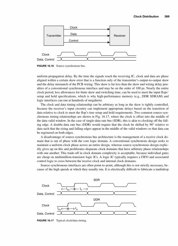
Clock Distribution 369
uniform propagation delay. By the time the signals reach the receiving IC, clock and data are phasealigned within a certain skew error that is a function only of the transmitter’s output-to-output skewand the delay mismatch of the PCB wiring. This skew is far less than the skew and wiring delay pen-alties of a conventional synchronous interface and may be on the order of 100 ps. Nearly the entireclock period, less allowances for finite skew and switching time, can be used to meet the input flops’setup and hold specifications, which is why high-performance memory (e.g., DDR SDRAM) andlogic interfaces can run at hundreds of megahertz.
The clock and data timing relationship can be arbitrary as long as the skew is tightly controlled,because the receiver’s input circuitry can implement appropriate delays based on the transition ofdata relative to clock to meet the flop’s true setup and hold requirements. Two common source-syn-chronous timing relationships are shown in Fig. 16.17, where the clock is offset into the middle ofthe data valid window. In the case of single-data rate bus (SDR), this is akin to clocking off the fall-ing edge. A double-data rate bus (DDR) would require that the clock be shifted by 90° relative todata such that the rising and falling edges appear in the middle of the valid windows so that data canbe registered on both edges.
A disadvantage of source-synchronous bus architecture is the management of a receive clock do-main that is out of phase with the core logic domain. A conventional synchronous design seeks tomaintain a uniform clock phase across an entire design, whereas source-synchronous design explic-itly gives up on this and proliferates disparate clock domains that have arbitrary phase relationshipswith one another. This trade-off in clock domain complexity is acceptable, because individual gatesare cheap on multimillion-transistor logic ICs. A logic IC typically requires a FIFO and associatedcontrol logic to cross between the receive clock and internal clock domains.
Source-synchronous interfaces are often point-to-point, although this is not strictly necessary, be-cause of the high speeds at which they usually run. It is electrically difficult to fabricate a multidrop
Transmitter Receiver
Clock
Data
Control
Clock
Data, Control
FIGURE 16.16 Source-synchronous bus.
tSU
Clock
Data, Control
SDR
tH
tSU
Clock
Data, Control
DDR
tH
FIGURE 16.17 Typical clock/data timing.
-Balch.book Page 369 Thursday, May 15, 2003 3:46 PM
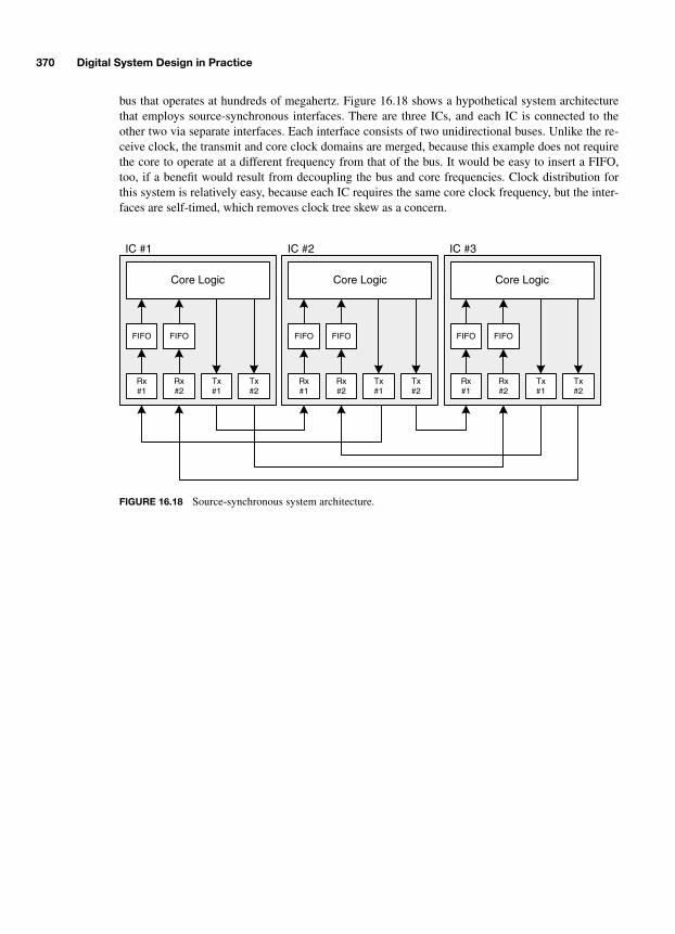
370 Digital System Design in Practice
bus that operates at hundreds of megahertz. Figure 16.18 shows a hypothetical system architecturethat employs source-synchronous interfaces. There are three ICs, and each IC is connected to theother two via separate interfaces. Each interface consists of two unidirectional buses. Unlike the re-ceive clock, the transmit and core clock domains are merged, because this example does not requirethe core to operate at a different frequency from that of the bus. It would be easy to insert a FIFO,too, if a benefit would result from decoupling the bus and core frequencies. Clock distribution forthis system is relatively easy, because each IC requires the same core clock frequency, but the inter-faces are self-timed, which removes clock tree skew as a concern.
Tx#1
Core Logic
FIFO
Rx#1
FIFO
Rx#2
Tx#2
IC #1 IC #2 IC #3
Tx#1
Core Logic
FIFO
Rx#1
FIFO
Rx#2
Tx#2
Tx#1
Core Logic
FIFO
Rx#1
FIFO
Rx#2
Tx#2
FIGURE 16.18 Source-synchronous system architecture.
-Balch.book Page 370 Thursday, May 15, 2003 3:46 PM
371
CHAPTER 17
Voltage Regulation and Power Distribution
Power is an obviously critical component of a system, but some engineers have bad reputations forinadequately planning a system’s voltage regulation and power distribution scheme. When power isan afterthought, luck sometimes works and sometimes does not. There is really no magic involved indesigning an appropriate power subsystem, and this chapter seeks to explain the main issues thatshould be taken into consideration. The purpose of this chapter is to provide a broad understandingof power regulation concepts and how they can be applied to implement the power regulation anddistribution circuitry in a digital system.
After many years of development and industry experience, we are fortunate to have at our dis-posal a broad array of off-the-shelf power regulation products. In concert with discrete semiconduc-tors, a system’s unique power requirements can be addressed with the appropriate tools. Manypower requirements can be handled with off-the-shelf regulators. When situations arise that require asemicustom approach, the gaps can be filled in with a basic understanding of voltage regulationtechniques.
Safety should be an overriding concern in all engineering disciplines, but safety is all the morecritical when dealing with power circuits. Power circuits may carry potentially lethal voltages andcurrents and must be treated with a healthy respect. Resist the urge to quickly prototype a power cir-cuit without taking the necessary time to study its thermal and electrical properties. Even if a powercircuit appears to operate properly for a few minutes, an improper design can eventually overheat,with disastrous results.
This chapter is organized in two basic sections: voltage regulation and power distribution. First,basic voltage regulation principles are discussed to provide an orientation to the subject. Thermalanalysis is then presented before any circuits are discussed, because thermal issues are fundamentalto all power circuits. A safe and reliable circuit must be designed to handle its intended power loadover its full range of operating conditions without overheating. The two subsequent sections dealwith methods of regulating voltage and current, encompassing diode-shunt and transistor series-reg-ulators. Off-the-shelf solutions are explored next to provide an understanding of the common inte-grated linear and switching regulators at an engineer’s disposal.
Once basic regulation techniques have been presented, important issues in power distribution arediscussed. Even the best regulator is useless without adequate means of conveying power to the load.Power distribution encompasses three basic themes: safety, reliability, and electrical integrity. Safetyand reliability issues of handling AC power, fuses, and adequate wiring are discussed. Power regula-tion schemes employing precertified off-the-shelf AC-to-DC supplies are encouraged because of theimproved safety of using known-good AC power modules. Finally, the use of low-inductance powerplanes and bypass capacitors is presented in the context of distributing power while preserving itselectrical integrity. A brief power subsystem design example is used to illustrate these concepts.
-Balch.book Page 371 Thursday, May 15, 2003 3:46 PM
Copyright 2003 by The McGraw-Hill Companies, Inc. Click Here for Terms of Use.

372 Digital System Design in Practice
17.1 VOLTAGE REGULATION BASICS
Power usually enters a system in a form dictated by its generation and distribution characteristicsrather than in a form required by the components within that system. Plugging a computer into a120 VAC wall outlet provides it with power in a form that was deemed efficient for generation anddistribution in the early twentieth century. Unlike light bulbs, digital logic chips do not run very wellif connected directly to 120 VAC, although they may emit a bright light for a brief period if con-nected in this manner! Rectifiers and the conversion between AC to DC has already been discussed,but this is only part of the solution to providing usable power to system components. Once the AChas been rectified to DC and filtered, the voltage probably does not meet the specifications of the cir-cuit. A rectified power input may not only have the wrong DC level, it probably has a good deal ofripple artifacts from the original AC input, as shown in Fig. 17.1.
An ideal voltage regulator provides a constant DC output without ripple regardless of the inputvoltage’s DC level and ripple. This applies not only to rectified AC power but also to power providedby batteries, solar cells, DC generators, and so on. Any time a system’s power input does not providethe supply voltage required by its components, a voltage regulator is necessary to perform this con-version. Most digital systems require at least one voltage regulator, because it is rare to find a powersource that provides the exact voltage required by digital and analog circuits. There are, however,some special-purpose ICs designed with wide supply voltage specifications so that they can be di-rectly connected to batteries without an intermediate voltage regulator. On the flip side, there aresystems that require multiple voltage regulators, because they contain circuitry with multiple supplyvoltage specifications. At one time, it was common to have a single +5-V digital supply. Now, it isnot uncommon to have 3.3-, 2.5-, 1.8-, and 1.5-V supplies in myriad configurations.
Most voltage regulators are the
step-down
variety—they provide a constant output voltage that islower than the input. There are many types of step-down regulators, as will be shown in the course ofthis chapter. Some applications require
step-up
regulators that provide a constant output that ishigher than the input. These applications are often low-power battery-operated devices in which a1.5- to 3-V battery is moderately stepped up to power a small circuit.
A voltage regulator must have access to some form of voltage reference to which it can compareits output to determine if the level is correct. Without a known reference, the regulator has no meansof measuring its output. This is analogous to measuring an object with a ruler, which is a knownlength reference. Without the reference, the object’s length remains unknown. The structure of ageneral voltage regulator is shown in Fig. 17.2.
The reference is powered directly by the arbitrary input voltage but maintains a constant outputvoltage subject to certain minimum operating conditions. A reference cannot maintain an outputvoltage higher than the input. Therefore, references usually provide low voltages that are comparedagainst a scaled-down feedback voltage from the output. This enables the regulator to function overa wider range of input levels. The two resistors implement a basic voltage divider that drives a feed-back comparator. These resistors are chosen to provide a feedback voltage equal to the reference atthe desired output voltage. When the feedback voltage falls below the reference, the comparator sig-
Rectified AC Power Filtered DC with Ripple
FIGURE 17.1 Ripple on a rectified AC power input.
-Balch.book Page 372 Thursday, May 15, 2003 3:46 PM
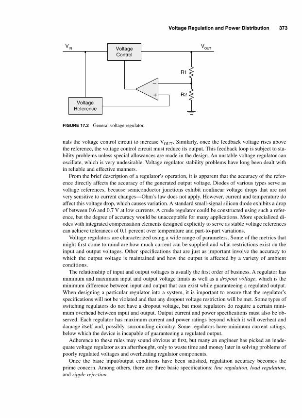
Voltage Regulation and Power Distribution 373
nals the voltage control circuit to increase V
OUT
. Similarly, once the feedback voltage rises abovethe reference, the voltage control circuit must reduce its output. This feedback loop is subject to sta-bility problems unless special allowances are made in the design. An unstable voltage regulator canoscillate, which is very undesirable. Voltage regulator stability problems have long been dealt within reliable and effective manners.
From the brief description of a regulator’s operation, it is apparent that the accuracy of the refer-ence directly affects the accuracy of the generated output voltage. Diodes of various types serve asvoltage references, because semiconductor junctions exhibit nonlinear voltage drops that are notvery sensitive to current changes—Ohm’s law does not apply. However, current and temperature doaffect this voltage drop, which causes variation. A standard small-signal silicon diode exhibits a dropof between 0.6 and 0.7 V at low currents. A crude regulator could be constructed using such a refer-ence, but the degree of accuracy would be unacceptable for many applications. More specialized di-odes with integrated compensation elements designed explicitly to serve as stable voltage referencescan achieve tolerances of 0.1 percent over temperature and part-to-part variations.
Voltage regulators are characterized using a wide range of parameters. Some of the metrics thatmight first come to mind are how much current can be supplied and what restrictions exist on theinput and output voltages. Other specifications that are just as important involve the accuracy towhich the output voltage is maintained and how the output is affected by a variety of ambientconditions.
The relationship of input and output voltages is usually the first order of business. A regulator hasminimum and maximum input and output voltage limits as well as a
dropout voltage
, which is theminimum difference between input and output that can exist while guaranteeing a regulated output.When designing a particular regulator into a system, it is important to ensure that the regulator’sspecifications will not be violated and that any dropout voltage restriction will be met. Some types ofswitching regulators do not have a dropout voltage, but most regulators do require a certain mini-mum overhead between input and output. Output current and power specifications must also be ob-served. Each regulator has maximum current and power ratings beyond which it will overheat anddamage itself and, possibly, surrounding circuitry. Some regulators have minimum current ratings,below which the device is incapable of guaranteeing a regulated output.
Adherence to these rules may sound obvious at first, but many an engineer has picked an inade-quate voltage regulator as an afterthought, only to waste time and money later in solving problems ofpoorly regulated voltages and overheating regulator components.
Once the basic input/output conditions have been satisfied, regulation accuracy becomes theprime concern. Among others, there are three basic specifications:
line regulation
,
load regulation
,and
ripple rejection
.
R2
VOUTVIN
R1
VoltageControl
VoltageReference
+
–
FIGURE 17.2 General voltage regulator.
-Balch.book Page 373 Thursday, May 15, 2003 3:46 PM

374 Digital System Design in Practice
Line regulation is the relationship between a change in the input (line) voltage and the outputvoltage and is expressed in either percentage or absolute magnitude terms. It is not uncommon tofind regulators with line regulation on the order of 0.01 percent. Such a regulator would exhibit anoutput swing of only 0.01 percent over the full range of the specified input voltage.
Load regulation is the relationship between a change in the load current and the output voltageand is also expressed as either a percentage or a magnitude. Regulators are available with load regu-lation on the order of 0.1 percent. This means that, over the full range of specified output current, theoutput voltage will not change by more than 0.1 percent.
Line and load regulation are not the only parameters affecting the DC output level of the regula-tor. These parameters characterize the voltage control element and feedback amplifier in the regula-tor. The operation of these components is only as good as the quality of the voltage reference and theapplied feedback voltage. High-quality DC power supplies can deliver 1 percent DC accuracy,meaning that the reference and feedback resistor network have a combined tolerance better than 1percent. A 3.3-V, 1 percent supply guarantees an output range from 3.267 to 3.333 V. Most digitalsystems use 5 percent supplies, because such accuracy is typically easy to achieve, and most com-mercial logic ICs are specified with V
CC
/V
DD
tolerances of no more than 5 percent. This is where thecommon 4.75- to 5.25-V operating range comes from when dealing with 5-V logic. Some logic ICsare specified with V
CC
/V
DD
tolerances of 10 percent, although fewer ICs are found with such looseratings these days because of the ease with which 5 percent supplies are implemented. It is easier fora semiconductor manufacturer or an analog circuit designer to build a system with a tighter supplyvoltage requirement, because the components do not have to operate over a wider range of condi-tions. Specifying all ICs with 1 percent requirements would make the vendors’ jobs easier, but itwould also result in more expense and complexity at the system level. Five percent is a good com-promise at the current state of technology.
Finally, ripple rejection is the ability of a regulator to block incoming ripple from feeding throughto the output. It is the ratio of the input ripple magnitude to the output ripple magnitude and is usu-ally expressed in decibels, because it is a large number for any effective regulator. Ripple rejectionspecifications of 50 to 80 dB are common. These specifications are often measured at 120 Hz, be-cause this is the ripple frequency resulting from a rectified 60 Hz AC input in North America andother parts of the world. Ripple rejection gets worse with increasing frequency, making a 120 Hzspecification worst case when compared to the 100-Hz ripple that would be observed from a rectified50-Hz AC input in Europe or Asia.
17.2 THERMAL ANALYSIS
Before heading straight into a discussion of voltage regulation techniques, it is appropriate to brieflyintroduce thermal analysis in the context of electronic components. Some energy will be dissipatedas heat during the process of converting an input voltage to an output voltage, regardless of the typeof regulator. All or most of the power in a typical system passes through voltage regulators, makingthem a concentrated point of heating. Without performing a basic thermal analysis, a power regula-tion component may be inadequately sized and cooled and could fail in a potentially dangerous man-ner. Melting circuits, fires, and even small explosions can result from poorly designed regulators. Agiven component, for example, can be designed to safely dissipate 10 W without heating exces-sively, but a similar component could fail while dissipating only 1 W if proper thermal design prac-tices are not followed.
Power regulation and thermal analysis are topics so intertwined that one cannot separate them andbe assured of a reliable and safe system. The best, most efficient regulator is worthless if it is oper-ated in a manner that causes it to overheat and fail.
-Balch.book Page 374 Thursday, May 15, 2003 3:46 PM
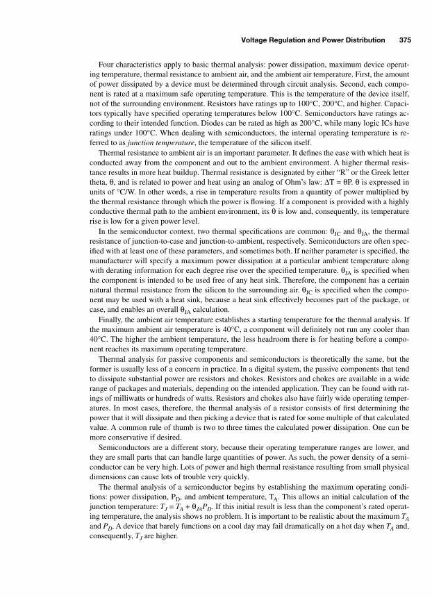
Voltage Regulation and Power Distribution 375
Four characteristics apply to basic thermal analysis: power dissipation, maximum device operat-ing temperature, thermal resistance to ambient air, and the ambient air temperature. First, the amountof power dissipated by a device must be determined through circuit analysis. Second, each compo-nent is rated at a maximum safe operating temperature. This is the temperature of the device itself,not of the surrounding environment. Resistors have ratings up to 100°C, 200°C, and higher. Capaci-tors typically have specified operating temperatures below 100°C. Semiconductors have ratings ac-cording to their intended function. Diodes can be rated as high as 200°C, while many logic ICs haveratings under 100°C. When dealing with semiconductors, the internal operating temperature is re-ferred to as
junction temperature
, the temperature of the silicon itself.Thermal resistance to ambient air is an important parameter. It defines the ease with which heat is
conducted away from the component and out to the ambient environment. A higher thermal resis-tance results in more heat buildup. Thermal resistance is designated by either “R” or the Greek lettertheta,
θ
, and is related to power and heat using an analog of Ohm’s law:
∆
T =
θ
P.
θ
is expressed inunits of °C/W. In other words, a rise in temperature results from a quantity of power multiplied bythe thermal resistance through which the power is flowing. If a component is provided with a highlyconductive thermal path to the ambient environment, its
θ
is low and, consequently, its temperaturerise is low for a given power level.
In the semiconductor context, two thermal specifications are common:
θ
JC
and
θ
JA
, the thermalresistance of junction-to-case and junction-to-ambient, respectively. Semiconductors are often spec-ified with at least one of these parameters, and sometimes both. If neither parameter is specified, themanufacturer will specify a maximum power dissipation at a particular ambient temperature alongwith derating information for each degree rise over the specified temperature.
θ
JA
is specified whenthe component is intended to be used free of any heat sink. Therefore, the component has a certainnatural thermal resistance from the silicon to the surrounding air.
θ
JC
is specified when the compo-nent may be used with a heat sink, because a heat sink effectively becomes part of the package, orcase, and enables an overall
θ
JA
calculation.Finally, the ambient air temperature establishes a starting temperature for the thermal analysis. If
the maximum ambient air temperature is 40°C, a component will definitely not run any cooler than40°C. The higher the ambient temperature, the less headroom there is for heating before a compo-nent reaches its maximum operating temperature.
Thermal analysis for passive components and semiconductors is theoretically the same, but theformer is usually less of a concern in practice. In a digital system, the passive components that tendto dissipate substantial power are resistors and chokes. Resistors and chokes are available in a widerange of packages and materials, depending on the intended application. They can be found with rat-ings of milliwatts or hundreds of watts. Resistors and chokes also have fairly wide operating temper-atures. In most cases, therefore, the thermal analysis of a resistor consists of first determining thepower that it will dissipate and then picking a device that is rated for some multiple of that calculatedvalue. A common rule of thumb is two to three times the calculated power dissipation. One can bemore conservative if desired.
Semiconductors are a different story, because their operating temperature ranges are lower, andthey are small parts that can handle large quantities of power. As such, the power density of a semi-conductor can be very high. Lots of power and high thermal resistance resulting from small physicaldimensions can cause lots of trouble very quickly.
The thermal analysis of a semiconductor begins by establishing the maximum operating condi-tions: power dissipation, P
D
, and ambient temperature, T
A
. This allows an initial calculation of thejunction temperature:
T
J
=
T
A
+
θ
JA
P
D
. If this initial result is less than the component’s rated operat-ing temperature, the analysis shows no problem. It is important to be realistic about the maximum
T
A
and
P
D
. A device that barely functions on a cool day may fail dramatically on a hot day when
T
A
and,consequently,
T
J
are higher.
-Balch.book Page 375 Thursday, May 15, 2003 3:46 PM

376 Digital System Design in Practice
As an example, consider a device housed in a TO-220 package,shown in Fig. 17.3, with
θ
JA
= 65°C/W. The TO-220 is a commonthree-leaded package for power semiconductors including diodes,transistors, and integrated voltage regulators. If
T
J(MAX)
= 150°Cand
T
A(MAX)
= 40°C, there is a 110°C temperature rise budget thatcorresponds to
P
D
=
∆
T
÷
θ
JA
= 1.6 W (always round down forsafety when dealing with thermal and power limits). If 1.6 W is in-sufficient for the application, there are several choices. The best op-tion is to reduce power consumption so that heat is less of aproblem in the first place. However, this is often not possible, giventhe design constraints. Failing that, either a larger package withlower
θ
JA
can be chosen, or the TO-220 can be attached to a heatsink to decrease the overall
θ
JA
. The TO-220 has a mounting hole tofacilitate heat sink attachment.
Heat sinks are very common, because packages have practical limitations on how low their
θ
JA
can be. Thermal resistance is a function of materials and surface area. A small package has limitedsurface area. A good heat sink is constructed of a material that has low thermal resistance (mostcommonly, aluminum or copper) and that has a large surface area to radiate heat into the air. When aheat sink is attached, the device’s
θ
JA
becomes irrelevant, and
θ
JC
becomes important, because it isthe thermal resistance through the package to another material that matters. A TO-220’s typical
θ
JC
is just 2.5°C/W—more than an order of magnitude better than
θ
JA
—because thermal conduction be-tween attached metal surfaces is far better than between metal and air.
With a heat sink attached to the package, the heat sink’s
θ
becomes relevant. Heat sinks are avail-able in a wide range of sizes according to how much power needs to be dissipated. Off-the-shelf heatsinks for TO-220 packages can be found with thermal resistances under 3°C/W in still air. The junc-tion between the heat sink and the IC package adds its own thermal resistance, which is often mini-mized via the application of thermally conductive grease. Assuming
θ
HEATSINK
= 3°C/W, the total
θ
JA
is now just 2.5 + 3 = 5.5°C/W. From a strictly thermal perspective, the device can now safely dis-sipate 110°C ÷
θ
TOTAL
= 20 W! This solves the heating problem, but does not automatically meanthat the semiconductor can handle this much power even when adequately cooled. Be sure to checkthe device’s inherent current and voltage ratings to see if they become the limiting factor when heatis accommodated.
Semiconductors intended for lower-power applications do not always have associated thermal resis-tance specifications. Instead, they are rated for a certain power dissipation at a given ambient tempera-ture, often 25°C—room temperature. If the ambient temperature exceeds the rating, a power deratingcurve or coefficient is provided that can be used to determine the safe power dissipation at a specifictemperature. For example, a device may be rated for 400 mW at
T
A
= 25°C with a derating coefficientof 3.2 mW/°C. This means that, if the actual maximum
T
A
is 40°C, the device’s power rating is reducedby
∆
T
A
×
3.2 mW/°C = 15°C
×
3.2 mW/°C = 48 mW, for an overall rating of just 352 mA.It pays to be conservative when designing power regulation circuits, both in terms of current/volt-
age headroom as well as thermal headroom. The life span of most components is reduced as temper-atures rise, so a cooler product is a more reliable product.
17.3 ZENER DIODES AND SHUNT REGULATORS
Perhaps the simplest type of voltage regulator is one formed by using a diode in a shunt circuit. Ashunt regulator, shown in Fig. 17.4, consists of a device that conducts excess current to ground tomaintain a fixed voltage between its two terminals. A series resistor, R
DROP
, serves as the voltage-
FIGURE 17.3 TO-220 package.
-Balch.book Page 376 Thursday, May 15, 2003 3:46 PM
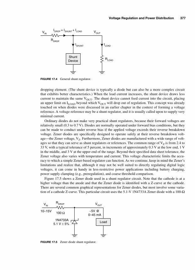
Voltage Regulation and Power Distribution 377
dropping element. (The shunt device is typically a diode but can also be a more complex circuitthat exhibits better characteristics.) When the load current increases, the shunt device draws lesscurrent to maintain the same V
OUT
. The shunt device cannot feed current into the circuit, placingan upper limit on I
LOAD
beyond which V
OUT
will drop out of regulation. This concept was alreadytouched on when diodes were discussed in an earlier chapter in the context of forming a voltagereference. A voltage reference may be a shunt regulator, and it is usually called upon to supply veryminimal current.
Ordinary diodes do not make very practical shunt regulators, because their forward voltages arerelatively small (0.3 to 0.7 V). Diodes are normally operated under forward bias conditions, but theycan be made to conduct under reverse bias if the applied voltage exceeds their reverse breakdownvoltage. Zener diodes are specifically designed to operate safely at their reverse breakdown volt-age—the Zener voltage, V
Z
. Furthermore, Zener diodes are manufactured with a wide range of volt-ages so that they can serve as shunt regulators or references. The common range of V
Z
is from 2.4 to33 V, with a typical tolerance of 5 percent, in increments of approximately 0.3 V at the low end, 1 Vin the middle, and 3 V at the upper end of the range. Beyond their specified data sheet tolerance, theZener voltage also varies with temperature and current. This voltage characteristic limits the accu-racy to which a simple Zener-based regulator can function. As we continue, keep in mind the Zener’slimitations and realize that, although it may not be well suited to directly regulating digital logicvoltages, it can come in handy in less-restrictive power applications including battery charging,power supply clamping (e.g., preregulation), and coarse threshold comparison.
Figure 17.5 shows a Zener diode used in a shunt regulator circuit. Note that the cathode is at ahigher voltage than the anode and that the Zener diode is identified with a Z-curve at the cathode.There are several common graphical representations for Zener diodes, but most involve some varia-tion of a cathode Z-curve. This particular circuit uses the 5.1-V 1N4733A Zener diode with a 100-
Ω
RLOAD
VOUTVIN
RDROP
ShuntDevice
IDROP = ISHUNT + ILOAD
ILOADISHUNT
FIGURE 17.4 General shunt regulator.
VOUTVINRDROP
100 Ω
Load
10–15V ~5V @0–45 mA
1N4733A5.1 V ± 5%
FIGURE 17.5 Zener diode shunt regulator.
-Balch.book Page 377 Thursday, May 15, 2003 3:46 PM

378 Digital System Design in Practice
series resistor to regulate an input of between 10 and 15 V down to approximately 5 V over a currentrange from 0 to 45 mA.
Aside from selecting a diode with the appropriate Zener voltage, a diode and resistor combinationmust be selected that can properly handle the circuit’s worst-case power dissipation. Many types ofregulators, including this one, operate by converting excess power into heat. The resistor is chosen tobe as large as possible to minimize power dissipation while maintaining sufficient current throughthe diode to establish the desired voltage. In this situation, the resistor is bounded at a maximumvalue by its voltage drop at the maximum load current with a minimum input voltage, 10 V. The volt-age drop in this situation is 4.9 V at 45 mA. 100
Ω
is chosen, because it is smaller than the calculatedvalue of 108
Ω
, thereby providing a guaranteed minimum excess current for the diode to remain ac-tive: 4 mA. The circuit must allow the diode to conduct sufficient current at all times to remain ac-tive. Otherwise, the diode may take too long to begin conducting when the load current drops,thereby allowing V
OUT
to exceed its specified range. The 1N4733A is characterized with Zener“knee” currents down to 1 mA, sufficiently below our 4-mA design point to remain active.
*
Under this most favorable circumstance of minimum input voltage and maximum load current,the resistor and diode dissipate a minimum of 240 mW and 20 mW, respectively, for a total of justover a 0.25 W. If the input remains at 10 V, but the load current drops to its minimum value, 0 mA,the diode must shunt the full current to ground, resulting in 250 mW dissipated by the diode.
As the input voltage rises to its maximum of 15 V, the regulator must convert more power intoheat. Now, the resistor must drop 9.9 V, burning 980 mW. This results in a current through the resis-tor of 100 mA, but the load is drawing only a maximum of 45 mA. Therefore, the diode must shuntthe difference, 55 mA, to ground, thereby dissipating 280 mW. Unfortunately, this is not the worst-case scenario. The load is rated at a minimum current of zero, meaning that the diode must be able toshunt the full 100 mA that flows through the resistor when the input is at its maximum. This equatesto a maximum diode power dissipation of 510 mW and an overall worst-case power dissipation forthe regulator of nearly 1.5 W.
After calculating the maximum operating conditions of the regulator components, we must verifythat they are within the manufacturers’ specifications. The resistor dissipates nearly 1 W. Finding aresistor that can safely dissipate this quantity of power is fairly easy: a 2- or 3-W power resistor canbe chosen. For the diode, a check of the data sheet confirms that the maximum current through thediode, 100 mA, is within the manufacturer’s specifications of a continuous Zener (reverse bias) cur-rent of 178 mA.
†
Next, we must ensure that the diode can handle 510 mW of con-tinuous power dissipation at the circuit’s maximum ambient air op-erating temperature, T
A(MAX)
, which we will assume to be 40°C. The1N4733A, manufactured in the axial-leaded DO-41 package shownin Fig. 17.6, has several relevant specifications:
‡
•
P
D(MAX)
= 1 W at 50°C, derate at 6.67 mW/°C above 50°C
•
T
J(MAX)
= 200°C
•
θ
JA
= 100°C/W
According to the first specification, P
D(MAX)
, we are operating safely. The power is approximatelyhalf the rated value, and T
A(MAX)
is under 50°C. Because the manufacturer also provides
θ
JA
, we can
* Zeners 1N4728A-1N4752A, Fairchild Semiconductor, 2001, p. 1.†
Ibid.
‡
Ibid.
CathodeAnode
FIGURE 17.6 DO-41 package.
-Balch.book Page 378 Thursday, May 15, 2003 3:46 PM
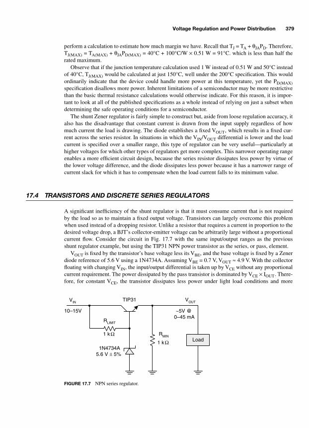
Voltage Regulation and Power Distribution 379
perform a calculation to estimate how much margin we have. Recall that T
J
= T
A
+
θ
JA
P
D
. Therefore,T
J(MAX)
= T
A(MAX)
+
θ
JA
P
D(MAX) = 40°C + 100°C/W × 0.51 W = 91°C. which is less than half therated maximum.
Observe that if the junction temperature calculation used 1 W instead of 0.51 W and 50°C insteadof 40°C, TJ(MAX) would be calculated at just 150°C, well under the 200°C specification. This wouldordinarily indicate that the device could handle more power at this temperature, yet the PD(MAX)specification disallows more power. Inherent limitations of a semiconductor may be more restrictivethan the basic thermal resistance calculations would otherwise indicate. For this reason, it is impor-tant to look at all of the published specifications as a whole instead of relying on just a subset whendetermining the safe operating conditions for a semiconductor.
The shunt Zener regulator is fairly simple to construct but, aside from loose regulation accuracy, italso has the disadvantage that constant current is drawn from the input supply regardless of howmuch current the load is drawing. The diode establishes a fixed VOUT, which results in a fixed cur-rent across the series resistor. In situations in which the VIN/VOUT differential is lower and the loadcurrent is specified over a smaller range, this type of regulator can be very useful—particularly athigher voltages for which other types of regulators get more complex. This narrower operating rangeenables a more efficient circuit design, because the series resistor dissipates less power by virtue ofthe lower voltage difference, and the diode dissipates less power because it has a narrower range ofcurrent slack for which it has to compensate when the load current falls to its minimum value.
17.4 TRANSISTORS AND DISCRETE SERIES REGULATORS
A significant inefficiency of the shunt regulator is that it must consume current that is not requiredby the load so as to maintain a fixed output voltage. Transistors can largely overcome this problemwhen used instead of a dropping resistor. Unlike a resistor that requires a current in proportion to thedesired voltage drop, a BJT’s collector-emitter voltage can be arbitrarily large without a proportionalcurrent flow. Consider the circuit in Fig. 17.7 with the same input/output ranges as the previousshunt regulator example, but using the TIP31 NPN power transistor as the series, or pass, element.
VOUT is fixed by the transistor’s base voltage less its VBE, and the base voltage is fixed by a Zenerdiode reference of 5.6 V using a 1N4734A. Assuming VBE = 0.7 V, VOUT ≈ 4.9 V. With the collectorfloating with changing VIN, the input/output differential is taken up by VCE without any proportionalcurrent requirement. The power dissipated by the pass transistor is dominated by VCE × IOUT. There-fore, for constant VCE, the transistor dissipates less power under light load conditions and more
VOUTVIN
1 k ΩLoad
10–15V ~5V @0–45 mA
1N4734A5.6 V ± 5%
RLIMIT
TIP31
RMIN
1 k Ω
FIGURE 17.7 NPN series regulator.
-Balch.book Page 379 Thursday, May 15, 2003 3:46 PM

380 Digital System Design in Practice
power with heavier loads. VCE cannot be reduced beyond the point of saturating the transistor be-cause this would result in the inability to maintain regulation.
Note the shunt resistor RMIN at the output. This resistor is present, because the minimum load cur-rent is zero. With zero load current, the transistor’s VBE circuit would not be complete, and the tran-sistor would be in cut-off. Maintaining the transistor in the active mode enables it to respond quicklyto changes in VCE. A 1-kΩ resistor is added to the output in parallel with the load to guarantee a min-imum output current of 4.9 mA so that the transistor remains active.
The regulator’s power dissipation is a function of the input voltage and the load current. Table17.1 summarizes the best- and worst-case power dissipation figures. Substantially lower power dissi-pation can be observed as compared to the shunt regulator discussed previously. The best-case powerof 93 mW is less than 260 mW for the shunt circuit. The worst-case power of 669 mW is also muchless than the shunt regulator’s 1,490 mW. As expected, the majority of the power is dissipated by theTIP31 pass transistor when the load current and VCE are at their maximum. The other componentsdissipate so little power that their thermal analysis is unnecessary in most situations.
The TIP31’s maximum collector current is 3 A, well over our 49-mA operating point.* It is alsorated for 2 W at an ambient temperature of 25°C and for 40 W at a case temperature of 25°C. Thesespecifications imply that the device is intended to be used with a heat sink under more than lightlyloaded conditions. Our present application has the transistor dissipating roughly one-quarter of thepower rating without a heat sink at 25°C. However, if we want the circuit to be usable up to 40°C,some additional consideration is necessary. The TIP 31 data sheet does not provide detailed thermalresistance information, only a power derating curve versus case temperature and a maximum junc-tion temperature of 150°C. Additional information is not needed if a heat sink is used, because thethermal resistance of the heat sink would be known, which would allow the determination of thecase temperature for a given power dissipation. Knowing the case temperature would allow using thepower derating curve to determine the safe operating limits of the transistor.
In the absence of information that applies specifically to our application, some estimates will haveto be made. First, the transistor is being operated at one-quarter of its rating at 25°C. This probablyprovides sufficient margin at 40°C. Second, we can use thermal resistance information from othersemiconductors packaged in a TO-220 package as a first-order approximation of the TIP31’s charac-teristics. Other TO-220 devices have θJA = 65°C/W. Using this information, the transistor would ex-perience a 33°C rise over ambient for TJ(MAX) = 73°C. While this is only an approximation, it is less
TABLE 17.1 Series Regulator Power Dissipation
ComponentVIN = 10 V
ILOAD = 0 mAVIN = 15 V
ILOAD = 45 mA
RLIMIT 19 mW 88 mW
Zener diode 25 mW 53 mW
RMIN 24 mW 24 mW
Transistor VCE 25 mW 504 mW
Total 93 mW 669 mW
* TIP31 Series, Fairchild Semiconductor, 2000, p. 1.
-Balch.book Page 380 Thursday, May 15, 2003 3:46 PM
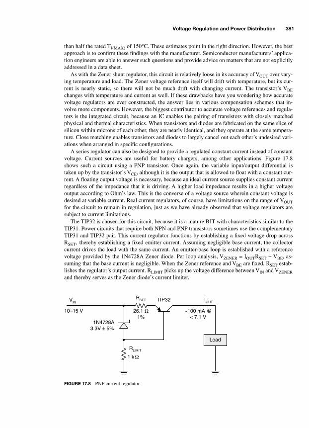
Voltage Regulation and Power Distribution 381
than half the rated TJ(MAX) of 150°C. These estimates point in the right direction. However, the bestapproach is to confirm these findings with the manufacturer. Semiconductor manufacturers’ applica-tion engineers are able to answer such questions and provide advice on matters that are not explicitlyaddressed in a data sheet.
As with the Zener shunt regulator, this circuit is relatively loose in its accuracy of VOUT over vary-ing temperature and load. The Zener voltage reference itself will drift with temperature, but its cur-rent is nearly static, so there will not be much drift with changing current. The transistor’s VBEchanges with temperature and current as well. If these drawbacks have you wondering how accuratevoltage regulators are ever constructed, the answer lies in various compensation schemes that in-volve more components. However, the biggest contributor to accurate voltage references and regula-tors is the integrated circuit, because an IC enables the pairing of transistors with closely matchedphysical and thermal characteristics. When transistors and diodes are fabricated on the same slice ofsilicon within microns of each other, they are nearly identical, and they operate at the same tempera-ture. Close matching enables transistors and diodes to largely cancel out each other’s undesired vari-ations when arranged in specific configurations.
A series regulator can also be designed to provide a regulated constant current instead of constantvoltage. Current sources are useful for battery chargers, among other applications. Figure 17.8shows such a circuit using a PNP transistor. Once again, the variable input/output differential istaken up by the transistor’s VCE, although it is the output that is allowed to float with a constant cur-rent. A floating output voltage is necessary, because an ideal current source supplies constant currentregardless of the impedance that it is driving. A higher load impedance results in a higher voltageoutput according to Ohm’s law. This is the converse of a voltage source wherein constant voltage isdesired at variable current. Real current regulators, of course, have limitations on the range of VOUTfor the circuit to remain in regulation, just as we have already observed that voltage regulators aresubject to current limitations.
The TIP32 is chosen for this circuit, because it is a mature BJT with characteristics similar to theTIP31. Power circuits that require both NPN and PNP transistors sometimes use the complementaryTIP31 and TIP32 pair. This current regulator functions by establishing a fixed voltage drop acrossRSET, thereby establishing a fixed emitter current. Assuming negligible base current, the collectorcurrent drives the load with the same current. An emitter-base loop is established with a referencevoltage provided by the 1N4728A Zener diode. Per loop analysis, VZENER = IOUTRSET + VBE, as-suming that the base current is negligible. When the Zener reference and VBE are fixed, RSET estab-lishes the regulator’s output current. RLIMIT picks up the voltage difference between VIN and VZENERand thereby serves as the Zener diode’s current limiter.
IOUTVIN
26.1 Ω1%
Load
10–15 V ~100 mA @< 7.1 V
1N4728A3.3V ± 5%
TIP32
1 k Ω
RLIMIT
RSET
FIGURE 17.8 PNP current regulator.
-Balch.book Page 381 Thursday, May 15, 2003 3:46 PM

382 Digital System Design in Practice
The current regulator cannot supply a constant 100 mA for all values of VOUT. As the load imped-ance is increased, there is a corresponding increase in VOUT, which reduces the difference with re-spect to VIN. This differential eventually forces the transistor into saturation when its collector-basejunction becomes forward biased. Using the estimate of VCE(SAT) = 0.3 V provides us with a mini-mum voltage drop across the transistor for the regulator to maintain 100 mA. The voltage dropacross RSET, 2.6 V, must also be factored into the VIN/VOUT differential. The maximum VOUT mustbe evaluated along with minimum VIN to analyze the limiting scenario: VOUT(MAX) = VIN(MIN) –2.6 V – 0.3 V = 7.1 V. This circuit can therefore be guaranteed to function properly up to 7.1 V. Ofcourse, if VIN is at the upper end of its range, VOUT can be higher as well. But the worst-case sce-nario is what should be used when specifying the guaranteed parameters of a circuit.
Analysis of the regulator’s dropout voltage shows that the drop across RSET is the dominant termwithin the regulator circuit. If dropout voltage is a concern, the drop across the resistor should beminimized. This is why a low-voltage Zener has been selected rather than a 5- or 6-V diode. Thedrop across RSET is the difference between VZENER and VBE. Minimizing VZENER minimizes thedrop across RSET.
Calculating power dissipation to perform a thermal analysis requires bounding the output voltageat a practical minimum, because the transistor’s power dissipation increases with increasing VCEand, hence, decreasing VOUT. RSET has a constant voltage drop at constant current, so it has constantpower dissipation of 0.26 W. For the sake of discussion, we can pick VOUT(MIN) = 0 V. Along withVIN(MAX) = 15 V, the power dissipation of the transistor is IOUT(VIN – IOUTRSET – VOUT) = 1.24 W.The TIP32 and TIP 31 have equivalent power and thermal ratings. The transistor is rated at 2 Wwithout a heat sink at an ambient temperature of 25°C, and a conservative design methodologymight call for a heat sink on the TO-220 package in this case. A heat sink enables calculation of thepackage temperature for a given power dissipation and ambient temperature, which in turn enablesus to take advantage of the manufacturer’s power derating curve expressed in terms of package tem-perature.
A small TO-220 heat sink can provide a thermal resistance of 30°C/W with natural convection.Much lower values are achievable when a fan is blowing air across the heat sink and with a largerheat sink. A temperature rise of 37°C is attained with PD = 1.24 W. Therefore, a 40°C ambient tem-perature would result in a transistor case temperature of 77°C. The TIP32’s power derating curveshows that the transistor is capable of over 20 W at this case temperature.* The heat sink thereby en-ables a very conservative design with minimal cost or complexity.
17.5 LINEAR REGULATORS
Most voltage and current regulation requirements, especially in digital systems, can be solved withease by using integrated off-the-shelf regulators that provide high-quality regulation characteristics.Constructing a regulator from discrete parts can be useful when its requirements are sufficiently out-side the mainstream to dictate a custom approach. However, designing a custom regulator bringswith it the challenges of meeting the load’s regulation requirements over a potentially wide range ofoperating conditions. Power supplies for digital circuits have the benefit that the voltages are com-mon across the industry. This has enabled semiconductor manufacturers to design broad families ofintegrated regulators that are preadjusted for common supply voltages: 5, 3.3, 2.5, 1.8, and 1.5 V.Manufacturers also offer adjustable regulators that can be readily customized to a specific outputvoltage. The result is the ability to treat regulators largely as “black boxes” once their overall charac-
* TIP32 Series, Fairchild Semiconductor, 2000, p. 2.
-Balch.book Page 382 Thursday, May 15, 2003 3:46 PM
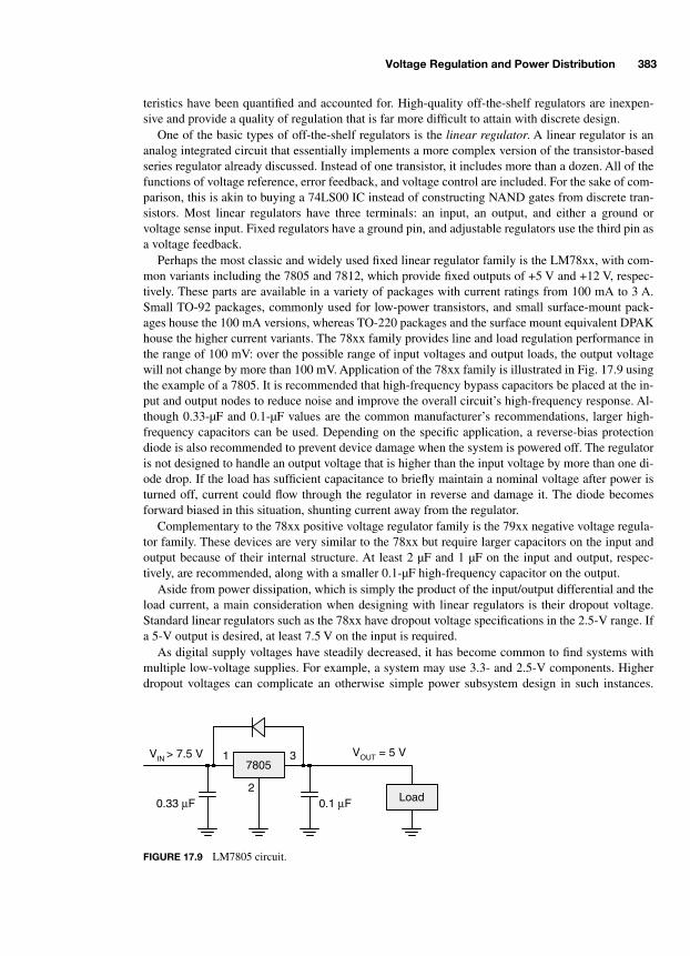
Voltage Regulation and Power Distribution 383
teristics have been quantified and accounted for. High-quality off-the-shelf regulators are inexpen-sive and provide a quality of regulation that is far more difficult to attain with discrete design.
One of the basic types of off-the-shelf regulators is the linear regulator. A linear regulator is ananalog integrated circuit that essentially implements a more complex version of the transistor-basedseries regulator already discussed. Instead of one transistor, it includes more than a dozen. All of thefunctions of voltage reference, error feedback, and voltage control are included. For the sake of com-parison, this is akin to buying a 74LS00 IC instead of constructing NAND gates from discrete tran-sistors. Most linear regulators have three terminals: an input, an output, and either a ground orvoltage sense input. Fixed regulators have a ground pin, and adjustable regulators use the third pin asa voltage feedback.
Perhaps the most classic and widely used fixed linear regulator family is the LM78xx, with com-mon variants including the 7805 and 7812, which provide fixed outputs of +5 V and +12 V, respec-tively. These parts are available in a variety of packages with current ratings from 100 mA to 3 A.Small TO-92 packages, commonly used for low-power transistors, and small surface-mount pack-ages house the 100 mA versions, whereas TO-220 packages and the surface mount equivalent DPAKhouse the higher current variants. The 78xx family provides line and load regulation performance inthe range of 100 mV: over the possible range of input voltages and output loads, the output voltagewill not change by more than 100 mV. Application of the 78xx family is illustrated in Fig. 17.9 usingthe example of a 7805. It is recommended that high-frequency bypass capacitors be placed at the in-put and output nodes to reduce noise and improve the overall circuit’s high-frequency response. Al-though 0.33-µF and 0.1-µF values are the common manufacturer’s recommendations, larger high-frequency capacitors can be used. Depending on the specific application, a reverse-bias protectiondiode is also recommended to prevent device damage when the system is powered off. The regulatoris not designed to handle an output voltage that is higher than the input voltage by more than one di-ode drop. If the load has sufficient capacitance to briefly maintain a nominal voltage after power isturned off, current could flow through the regulator in reverse and damage it. The diode becomesforward biased in this situation, shunting current away from the regulator.
Complementary to the 78xx positive voltage regulator family is the 79xx negative voltage regula-tor family. These devices are very similar to the 78xx but require larger capacitors on the input andoutput because of their internal structure. At least 2 µF and 1 µF on the input and output, respec-tively, are recommended, along with a smaller 0.1-µF high-frequency capacitor on the output.
Aside from power dissipation, which is simply the product of the input/output differential and theload current, a main consideration when designing with linear regulators is their dropout voltage.Standard linear regulators such as the 78xx have dropout voltage specifications in the 2.5-V range. Ifa 5-V output is desired, at least 7.5 V on the input is required.
As digital supply voltages have steadily decreased, it has become common to find systems withmultiple low-voltage supplies. For example, a system may use 3.3- and 2.5-V components. Higherdropout voltages can complicate an otherwise simple power subsystem design in such instances.
VOUT = 5 VVIN > 7.5 V
Load
7805
0.33 µF 0.1 µF
1
2
3
FIGURE 17.9 LM7805 circuit.
-Balch.book Page 383 Thursday, May 15, 2003 3:46 PM

384 Digital System Design in Practice
Clearly, a regulator with a 2.5-V dropout voltage is not capable of producing 2.5 V from 3.3 V. Fur-thermore, when the dropout voltage is on par with the output voltage, the regulator dissipates asmuch power as the load consumes! The semiconductor industry saw these problems emerging anddeveloped families of low dropout (LDO) regulators with dropout voltages well under 0.5 V. Thereare a wide variety of LDOs on the market today, but they are no longer members of standard familiessuch as the 78xx. Each manufacturer has its own product line. LDOs are advantageous not only be-cause of more flexible input/output voltage relationships, but also because they enable lower powerdissipation for a given load current. With a voltage differential of just 0.2 to 0.3 V, a 5-A regulatordissipates an order of magnitude less power than an older 2-V dropout device. These regulators aremanufactured by companies including Fairchild Semiconductor, Linear Technology, Maxim, Na-tional Semiconductor, and Texas Instruments.
When an output voltage is desired that is not supported by a fixed regulator, adjustable linear reg-ulators such as the ubiquitous LM317 and LM337 can be used for positive and negative voltages, re-spectively. These devices have an adjustment pin, instead of a ground pin, that is used to vary theoutput voltage. A basic LM317 circuit is shown in Fig. 17.10. Note the use of a reverse-bias protec-tion diode as employed previously for the fixed regulator. Additionally, a larger capacitor is recom-mended at the output to improve stability caused by internal differences with the 78xx fixedregulator.
The real difference is in the LM317’s voltage adjustment mechanism. An internal circuit main-tains a fixed 1.25 V between the output and adjustment pins, resulting in a current through R1 deter-mined by its resistance. This current is also referred to as the programming current. Assuming thatnegligible current flows into the adjustment pin, an accurate approximation is that the currentthrough R1 passes through R2 as well, creating a voltage drop across R2. The drop across R2 plusthe 1.25 V across R1 yields the regulated output voltage,
Typical resistance values for R1 are relatively small, ranging between 120 and 330 Ω. Values forR2 are larger so that higher voltages can be developed as necessary. It is advantageous to selectsmaller values for R1 and R2 so that the assumption of zero current through the adjustment pin ismore accurate. The actual adjustment pin current, IADJ, is a maximum of 100 µA.* In our example,
* LM317, National Semiconductor, 2001, p. 2.
VOUT = 3.3 VVIN > 5.8 V
Load
317
0.1 µF 0.1 µF
VIN
ADJ
VOUT
10 µF200 ΩR1
412 ΩR2
1%
1%
FIGURE 17.10 LM317 circuit.
V OUT 1.25 1 R2R1-------+
=
-Balch.book Page 384 Thursday, May 15, 2003 3:46 PM
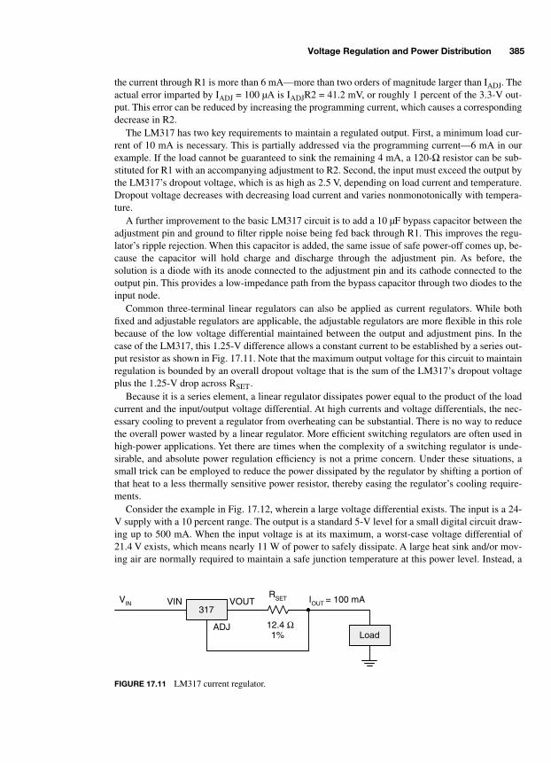
Voltage Regulation and Power Distribution 385
the current through R1 is more than 6 mA—more than two orders of magnitude larger than IADJ. Theactual error imparted by IADJ = 100 µA is IADJR2 = 41.2 mV, or roughly 1 percent of the 3.3-V out-put. This error can be reduced by increasing the programming current, which causes a correspondingdecrease in R2.
The LM317 has two key requirements to maintain a regulated output. First, a minimum load cur-rent of 10 mA is necessary. This is partially addressed via the programming current—6 mA in ourexample. If the load cannot be guaranteed to sink the remaining 4 mA, a 120-Ω resistor can be sub-stituted for R1 with an accompanying adjustment to R2. Second, the input must exceed the output bythe LM317’s dropout voltage, which is as high as 2.5 V, depending on load current and temperature.Dropout voltage decreases with decreasing load current and varies nonmonotonically with tempera-ture.
A further improvement to the basic LM317 circuit is to add a 10 µF bypass capacitor between theadjustment pin and ground to filter ripple noise being fed back through R1. This improves the regu-lator’s ripple rejection. When this capacitor is added, the same issue of safe power-off comes up, be-cause the capacitor will hold charge and discharge through the adjustment pin. As before, thesolution is a diode with its anode connected to the adjustment pin and its cathode connected to theoutput pin. This provides a low-impedance path from the bypass capacitor through two diodes to theinput node.
Common three-terminal linear regulators can also be applied as current regulators. While bothfixed and adjustable regulators are applicable, the adjustable regulators are more flexible in this rolebecause of the low voltage differential maintained between the output and adjustment pins. In thecase of the LM317, this 1.25-V difference allows a constant current to be established by a series out-put resistor as shown in Fig. 17.11. Note that the maximum output voltage for this circuit to maintainregulation is bounded by an overall dropout voltage that is the sum of the LM317’s dropout voltageplus the 1.25-V drop across RSET.
Because it is a series element, a linear regulator dissipates power equal to the product of the loadcurrent and the input/output voltage differential. At high currents and voltage differentials, the nec-essary cooling to prevent a regulator from overheating can be substantial. There is no way to reducethe overall power wasted by a linear regulator. More efficient switching regulators are often used inhigh-power applications. Yet there are times when the complexity of a switching regulator is unde-sirable, and absolute power regulation efficiency is not a prime concern. Under these situations, asmall trick can be employed to reduce the power dissipated by the regulator by shifting a portion ofthat heat to a less thermally sensitive power resistor, thereby easing the regulator’s cooling require-ments.
Consider the example in Fig. 17.12, wherein a large voltage differential exists. The input is a 24-V supply with a 10 percent range. The output is a standard 5-V level for a small digital circuit draw-ing up to 500 mA. When the input voltage is at its maximum, a worst-case voltage differential of21.4 V exists, which means nearly 11 W of power to safely dissipate. A large heat sink and/or mov-ing air are normally required to maintain a safe junction temperature at this power level. Instead, a
IOUT = 100 mAVIN
Load
317VIN
ADJ
VOUT
12.4 Ω
RSET
1%
FIGURE 17.11 LM317 current regulator.
-Balch.book Page 385 Thursday, May 15, 2003 3:46 PM

386 Digital System Design in Practice
27-Ω dropping resistor is inserted before the regulator. The dropping resistor is sized based on theload current, the minimum input voltage, and the regulator’s dropout voltage. Working with a con-servative dropout voltage of 3 V and a minimum input level of 21.6 V, the resistor must drop a max-imum of 13.6 V at 500 mA. The closest standard resistor value, 27 Ω, yields a drop of 13.5 V atmaximum load with a power dissipation of 6.75 W. Finding a power resistor that can safely dissi-pate about 7 W is not a problem. This reduces the power dissipated by the LM7805 to just 3.1 V ×500 mA ≈ 1.6 W. However, the worst-case power dissipation occurs when the input is at its maxi-mum of 26.4 V. The increased differential of 7.9 V results in a power dissipation of approximately4 W, as expected. We did not save any power, but the regulator’s share of the power has been de-creased by more than 60 percent, and it is much easier to cool 4 W than 11 W.
Linear regulators provide the easiest and least troublesome manner by which to provide a digitalcircuit with clean power. They work without causing problems as long as proper thermal analysis isperformed and they are kept from overheating. The main reason for not using a linear regulator isits inefficiency, particularly at higher input/output voltage differentials. It is quite convenient to usea linear regulator to derive 3.3 V from 5 V at currents under 1 A. Power dissipation becomes a big-ger problem when dealing with several amps. When tens of amps are required, the thermal problembecomes critical, and a more efficient alternative must often be found in the form of a switchingregulator.
17.6 SWITCHING REGULATORS
An ideal power regulator would achieve 100 percent efficiency by drawing only as much power fromthe source as required by the load. Assuming that the input and output voltages are unequal, the idealregulator would convert a supply current into a different load current to maintain constant power un-der two different voltages. A linear regulator is nonideal, because it is inherently dissipative—it sim-ply discards the excess power not required by the load, because it cannot convert an input current intoan unequal output current. Switching regulators approach the ideal much more closely, because theyare able to perform the current conversion process. Finite power losses in the switching regulator’scomponents are what cause it to deviate from ideal efficiency. Depending on the input/output charac-teristics and the circuit used, efficiencies between 80 and 95 percent are realistically achievable.
Switching regulators operate by alternately applying and removing input power from a passiveLC circuit. Figure 17.13 shows a simplified conceptual step-down regulator circuit, often called abuck regulator. The switching element alternately connects the inductor to the input and ground.When the switch selects the input, current flows through the inductor and charges the capacitor. Dur-ing this time, the inductor develops a magnetic field resulting from the current passing through it. Aninductor resists changes in current, because a current change disrupts its magnetic field. Whereas a
VOUT = 5 V@ 500 mA
VIN = 24 V± 10%
Load
78051
2
3RDROP
27 Ω
VINREG > 8.1 V
FIGURE 17.12 Shifting power dissipation to a resistor.
-Balch.book Page 386 Thursday, May 15, 2003 3:46 PM
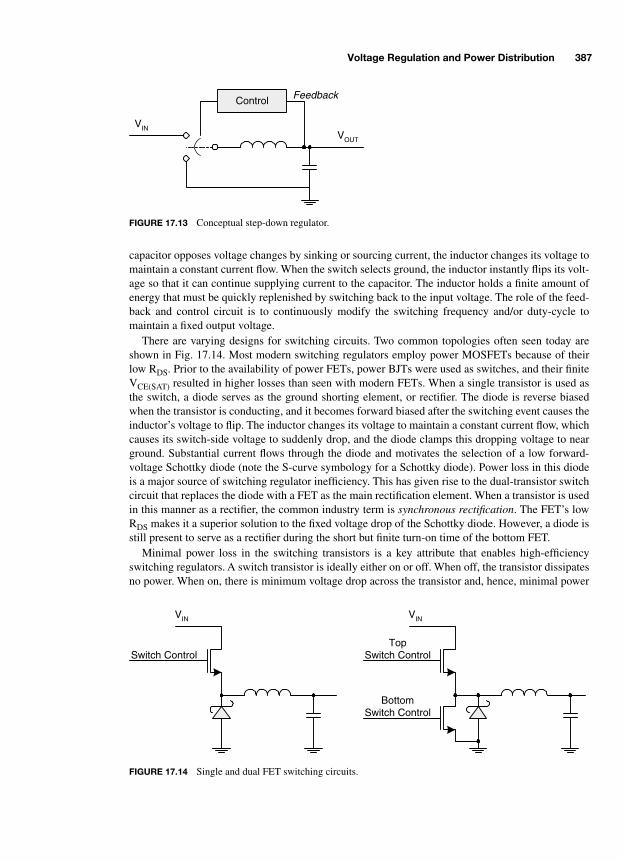
Voltage Regulation and Power Distribution 387
capacitor opposes voltage changes by sinking or sourcing current, the inductor changes its voltage tomaintain a constant current flow. When the switch selects ground, the inductor instantly flips its volt-age so that it can continue supplying current to the capacitor. The inductor holds a finite amount ofenergy that must be quickly replenished by switching back to the input voltage. The role of the feed-back and control circuit is to continuously modify the switching frequency and/or duty-cycle tomaintain a fixed output voltage.
There are varying designs for switching circuits. Two common topologies often seen today areshown in Fig. 17.14. Most modern switching regulators employ power MOSFETs because of theirlow RDS. Prior to the availability of power FETs, power BJTs were used as switches, and their finiteVCE(SAT) resulted in higher losses than seen with modern FETs. When a single transistor is used asthe switch, a diode serves as the ground shorting element, or rectifier. The diode is reverse biasedwhen the transistor is conducting, and it becomes forward biased after the switching event causes theinductor’s voltage to flip. The inductor changes its voltage to maintain a constant current flow, whichcauses its switch-side voltage to suddenly drop, and the diode clamps this dropping voltage to nearground. Substantial current flows through the diode and motivates the selection of a low forward-voltage Schottky diode (note the S-curve symbology for a Schottky diode). Power loss in this diodeis a major source of switching regulator inefficiency. This has given rise to the dual-transistor switchcircuit that replaces the diode with a FET as the main rectification element. When a transistor is usedin this manner as a rectifier, the common industry term is synchronous rectification. The FET’s lowRDS makes it a superior solution to the fixed voltage drop of the Schottky diode. However, a diode isstill present to serve as a rectifier during the short but finite turn-on time of the bottom FET.
Minimal power loss in the switching transistors is a key attribute that enables high-efficiencyswitching regulators. A switch transistor is ideally either on or off. When off, the transistor dissipatesno power. When on, there is minimum voltage drop across the transistor and, hence, minimal power
Feedback
VOUT
VIN
Control
FIGURE 17.13 Conceptual step-down regulator.
VIN VIN
BottomSwitch Control
TopSwitch ControlSwitch Control
FIGURE 17.14 Single and dual FET switching circuits.
-Balch.book Page 387 Thursday, May 15, 2003 3:46 PM

388 Digital System Design in Practice
dissipation. Switching control circuits seek to turn transistors on and off as rapidly as possible tominimize the time spent in a region of higher voltage and current. The drive strength required to rap-idly switch a large FET can be substantial, because a larger gate results in higher capacitance thatmust be charged to change the transistor’s state. In reality, the finite on-off FET switching times areanother significant source of power loss.
Aside from their high efficiency, switchers are extremely flexible, because they can do more thanregulate down. Step-up regulators, often called boost regulators, can convert a lower input voltageinto a higher output voltage. Inverting regulators can generate negative output voltages from a posi-tive input. Switchers can also be designed for buck-boost operation, whereby an output can be gener-ated from an input that is near the output level. This is a very useful feature for some applications,because it bypasses the problem of dropout voltage. Battery-powered portable devices commonlyuse step-up or buck-boost regulators because of the cost and size advantage of using fewer batterycells. Without a switcher, such a device would require more cells to meet the minimum dropout volt-age of a linear regulator.
Each type of switching regulator has a different topology. Most contain FETs, diodes, inductors,and capacitors. Some low-current switchers are now available that do not need inductors. A com-plete presentation of switching power supply circuit design is unnecessary in the context of mostdigital systems, because semiconductor manufacturers have done an excellent job of producing inte-grated switching regulator ICs that are easy to use by following recommended circuit and connec-tion diagrams. Perhaps the easiest way to use a switching regulator is to purchase an off-the-shelfmodule that already has the full circuit assembled and tested. Companies including Datel, Texas In-struments, and Vicor offer these ready-to-use modules.
More flexibility (and more work!) is possible when discrete ICs are used. Linear Technology,Maxim, and National Semiconductor offer wide varieties of switching regulator controller ICs thatrequire the addition of FETs, inductors, capacitors, diodes, and resistors. (Some low-power regulatorICs incorporate the FET switch on-chip to reduce circuit complexity.) These circuits can be fullycustomized for individual applications, and manufacturers supply detailed example circuits and doc-umentation to assist in the design effort. As with any semicustom design, more flexibility is possiblein terms of the circuit layout to squeeze into small spaces. The trade-off is increased design effort toensure that numerous discrete components operate properly.
Whatever implementation path is chosen, the incorporation of switching regulators into a systembrings with it a set of issues that are either not present or not as potentially troublesome when usinglinear regulators. A switching regulator introduces noise and ripple because of its high-current on-offoperation. Many switcher design issues revolve around minimizing this noise and ripple. The selec-tion of the inductor and capacitors is very important. An IC vendor will usually recommend a partic-ular inductor for a given switching frequency and output current. Because power inductors can getquite large, a current trend is to use smaller inductors at higher switching frequencies with the conse-quence of introducing higher-frequency noise into the system. If the high-frequency noise cannot beadequately filtered, a larger inductor may be used at a lower frequency.
Attenuating ripple and noise generated by the switching regulator is accomplished in large part byusing high-quality capacitors with extremely low equivalent series resistance, or ESR. The capaci-tors’ ESR must be minimized because of the high current spikes sent through the inductor by theswitching element. Each current spike will develop a voltage across the capacitor’s finite ESR.Higher resistance means higher voltage ripple. Ideally, ceramic surface-mount capacitors would beused because of their excellent high-frequency characteristics. Some switchers do use these capaci-tors, but their use is limited, because ceramics do not provide very high capacitances. High-powerswitchers require large capacitors rated at hundreds or thousands of microfarads. Tantalum and alu-minum electrolytic capacitors are commonly used in switcher circuits. Normal electrolytics do nothave adequate ESR for many switching applications, but manufacturers such as AVX, NIC, Nichi-
-Balch.book Page 388 Thursday, May 15, 2003 3:46 PM
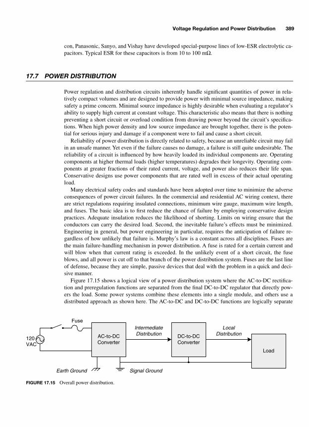
Voltage Regulation and Power Distribution 389
con, Panasonic, Sanyo, and Vishay have developed special-purpose lines of low-ESR electrolytic ca-pacitors. Typical ESR for these capacitors is from 10 to 100 mΩ.
17.7 POWER DISTRIBUTION
Power regulation and distribution circuits inherently handle significant quantities of power in rela-tively compact volumes and are designed to provide power with minimal source impedance, makingsafety a prime concern. Minimal source impedance is highly desirable when evaluating a regulator’sability to supply high current at constant voltage. This characteristic also means that there is nothingpreventing a short circuit or overload condition from drawing power beyond the circuit’s specifica-tions. When high power density and low source impedance are brought together, there is the poten-tial for serious injury and damage if a component were to fail and cause a short circuit.
Reliability of power distribution is directly related to safety, because an unreliable circuit may failin an unsafe manner. Yet even if the failure causes no damage, a failure is still quite undesirable. Thereliability of a circuit is influenced by how heavily loaded its individual components are. Operatingcomponents at higher thermal loads (higher temperatures) degrades their longevity. Operating com-ponents at greater fractions of their rated current, voltage, and power also reduces their life span.Conservative designs use power components that are rated well in excess of their actual operatingload.
Many electrical safety codes and standards have been adopted over time to minimize the adverseconsequences of power circuit failures. In the commercial and residential AC wiring context, thereare strict regulations requiring insulated connections, minimum wire gauge, maximum wire length,and fuses. The basic idea is to first reduce the chance of failure by employing conservative designpractices. Adequate insulation reduces the likelihood of shorting. Limits on wiring ensure that theconductors can carry the desired load. Second, the inevitable failure’s effects must be minimized.Engineering in general, but power engineering in particular, requires the anticipation of failure re-gardless of how unlikely that failure is. Murphy’s law is a constant across all disciplines. Fuses arethe main failure-handling mechanism in power distribution. A fuse is rated for a certain current andwill blow when that current rating is exceeded. In the unlikely event of a short circuit, the fuseblows, and all power is cut off to that branch of the power distribution system. Fuses are the last lineof defense, because they are simple, passive devices that deal with the problem in a quick and deci-sive manner.
Figure 17.15 shows a logical view of a power distribution system where the AC-to-DC rectifica-tion and preregulation functions are separated from the final DC-to-DC regulator that directly pow-ers the load. Some power systems combine these elements into a single module, and others use adistributed approach as shown here. The AC-to-DC and DC-to-DC functions are logically separate
AC-to-DCConverter
120VAC
IntermediateDistribution
LocalDistribution
Fuse
DC-to-DCConverter
Earth Ground Signal Ground
Load
FIGURE 17.15 Overall power distribution.
-Balch.book Page 389 Thursday, May 15, 2003 3:46 PM

390 Digital System Design in Practice
entities for a couple of reasons. First, they are usually associated with different levels of safety stan-dards. AC power supplies must conform to strict standards, because they have the potential to shortcircuit an AC wiring system with the resultant risk of serious injury and damage. Second, DC-to-DCconverters are tailored specifically to the voltages required by a digital logic circuit, whereas ACpower supplies can provide more standardized voltages given the widespread availability of DC reg-ulators.
The example also shows two distinct ground nodes: Earth ground and signal ground. A groundedAC wall outlet or other connection provides an absolute 0-V Earth ground connection into which ex-cess charge can drain. This path prevents the accumulation of charge to the point of damaging sensi-tive electronic components when a sudden electrostatic discharge may occur. It also ties separatepieces of equipment to the same ground potential so that they can be connected without adverse con-sequences. For example, if a printer and a computer are both connected via a cable, and each has adifferent ground potential, a ground loop may develop whereby unexpected current flows betweenthe two dissimilar voltages. A ground loop can be disruptive to communication between the printerand computer by manifesting itself as noise on the cable. In contrast to Earth ground, signal groundis the return path to the voltage regulators. Signal and Earth ground are usually connected so thatthere is a uniform DC ground potential throughout a system. However, many styles exist for makingthis connection. Some engineers and situations favor connecting the two grounds at a single point,often in the AC power supply. Others favor connecting the grounds at many points throughout thesystem. Grounding is an important topic that is discussed later in the context of signal integrity.
Given their different treatment, different symbols are used for each type of ground. Purists have avalid argument in favor of consistent representation for each type of ground. When drawing circuitdiagrams that must pass official certification standards, consistent representation may be enforced.In other circumstances, it is common for individuals to use whatever representation they prefer.When multiple ground symbols are present in a circuit diagram, the meaning of each symbol shouldbe explicitly determined, because different engineers and companies use their own styles.
As with household AC wiring, strict safety standards should always be observed when using AC-to-DC power supplies. Underwriters Laboratories (UL) has become the de facto standard for safeproduct certification in the United States, and UL certification is widely considered a mandatory re-quirement despite not always being dictated by law. All reputable AC power supply vendors seek ULcertification before offering their products for sale. Safe power supply design has long since becomea well understood and economical practice, and there is no significant burden on the system designand no incentive—financial or otherwise—to not employ a certified design. When designing a digi-tal system, it is almost always best to purchase a precertified AC power supply module from a thirdparty. Well known power supply vendors include Artesyn, Astec, Cherokee, Condor, and Lambda.These power supplies incorporate standard safety features including overload protection devices thatautomatically shut down the supply when it gets too hot or is called upon to source too much current.Some supplies contain internal fuses and are ready to plug into a wall outlet. Others require that aseparate AC wiring harness with fuse be connected.
Off-the-shelf power supplies are available in wide varieties of overall wattages and combinationsof output voltages and currents. In many cases, a single module can directly provide a digital sys-tem’s necessary voltage supplies. There are also many instances in which a digital system has volt-age and current requirements that are not directly served by one of these off-the-shelf configurations.The proliferation of low-voltage digital supplies (e.g., 2.5, 1.8, and 1.5 V) has decreased the likeli-hood of a one-size-fits-all power supply.
Safety requirements for DC-to-DC converters are usually less stringent than for AC-to-DC con-verters, but the same concepts of fusing and overload protection can be applied. In applications inwhich a DC power connection is externally accessible by the end-user, fusing and current limitingprecautions may be required for safety certification. Many switching regulator modules contain
-Balch.book Page 390 Thursday, May 15, 2003 3:46 PM

Voltage Regulation and Power Distribution 391
overload protection mechanisms that shut down in the event of excessive current draw. Safety stan-dards for DC-to-DC converters are less uniform and strict, because it is often sufficient to rely on thesafety cut-off mechanisms in the AC power module. If a DC regulator fails, the worst-case scenariois often that the AC supply’s overload protection will be activated and prevent damage to otherequipment and the AC wiring infrastructure.
Whenever power is distributed between two points, the conductors carrying that current must beadequately sized for the flow. Wires have current ratings based on their resistance, the ambient oper-ating temperature, the maximum allowable insulation temperature, and the number of wires bundledtogether. It is important to conservatively specify wire capacity, because wire has a positive temper-ature coefficient, meaning that resistance increases with temperature. If a wire is operated beyond itssafe capacity, a dangerous situation can develop in which heating increases resistance, which causesmore heating in a self-destructive cycle. Wire manufacturers should always be consulted on the rat-ings for their products when selecting the necessary gauge wires for an application. The AmericanWire Gauge (AWG) standard provides a measure of wire size, with thicker wires indicated bysmaller gauge numbers. Table 17.2 lists the resistance of solid copper wire per 1000 ft (304.8 m) at25°C.* Current ratings are based on the allowable temperature rise over ambient, which is why awire’s environment directly affects its rating. AC wires enclosed in the walls of your home are ratedmore conservatively because of the risk of fire in confined spaces. The conservative use of lower-gauge wire results in less power loss and heating, with a resulting increase in safety and reliability.
An example of a distributed power regulation scheme is shown in Fig. 17.16. This system uses anoff-the-shelf AC-to-DC power supply to provide a 12-VDC intermediate power bus. Common inter-mediate voltages include 48, 24, 12, and 5 V. The advantage of using a higher voltage is less currentflow through the intermediate distribution wiring for a given power level and hence lower resistivelosses (PD = I2R) in that wiring. Lower voltages have the benefit of easier component selection be-cause of the lower voltage ratings. When using a switching regulator, there is a compromise betweenvery low and very high input voltages. Too high an input requires a small switching duty cycle,which results in higher losses as the transistors turn on and off more often relative to the time thatthey are in a static state. Too low an input causes higher current to be drawn from the source, whichleads to higher I2R losses in the regulator components. Often, 12 V is a good compromise betweenswitching losses and easier regulator design. Additionally, some systems require 12 V for analog in-terface circuits or low-power motors such as a disk drive. This system can use whatever 12-V powersupply is easily available, as long as its capacity is greater than 43 W.
* The ARRL Handbook for Radio Amateurs, American Radio Relay League, 1994, pp. 35–36.
TABLE 17.2 Resistance of Solid Copper Wire at 25°C
Wire Gauge (AWG) Ω per 1000 ft (304.8 m) Wire Gauge (AWG) Ω per 1000 ft (304.8 m)
30 104 20 10.0
28 65 18 6.4
26 41 16 4.0
24 26 14 2.5
22 16 12 1.6
-Balch.book Page 391 Thursday, May 15, 2003 3:46 PM

392 Digital System Design in Practice
The fact that most systems can rely on an off-the-shelf AC power supply to provide an adequatelevel of safety enables a design style of selecting a certified AC supply with an adequate power rat-ing and then using a custom combination of regulators to provide the desired logic-level voltages.The advantage to this approach is not requiring the perfect AC supply that provides every voltage atthe correct current rating. Instead, an overall system power requirement is calculated and a supply isfound that provides a suitable intermediate voltage at or above that level. In this example, the finalvoltages are needed as follows: 12 V at 250 mA, 5 V at 2 A, 3.3 V at 5 A, and 2.5 V at 3 A. It is de-cided to create the 5- and 3.3-V supplies with switching regulators and use a low dropout linear reg-ulator to provide 2.5 V from 3.3 V, which is why the 3.3-V regulator must supply sufficient currentfor both the 3.3-V and 2.5-V needs. It is assumed that the switching regulators will operate with 90percent efficiency and therefore require approximately 43 W from the AC power supply.
Taking a distributed approach means that, if the system specifications ever change to require dif-ferent voltages, the proven AC supply is unaffected as long as the overall power level remains con-stant and the DC regulators can be adjusted as necessary. In many cases, adjusting the DC regulatorsis as simple as changing the value of a voltage-sensing feedback resistor.
A separate AC power supply module is often connected to the main circuit board with a wiringharness. In this case, wire must be chosen to safely carry 3.6 A at 12 V. Twenty-four gauge wire isadequate for the task and a more conservative choice is 22 gauge. The best results for distributingthe regulated 5-, 3.3-, and 2.5-V supplies are achieved by using complete PCB planes or very widecopper paths to connect the regulator outputs to the various ICs and components that they serve.Distributing these final logic-level power supplies segues directly into electrical integrity issues.
17.8 ELECTRICAL INTEGRITY
An ideal power distribution system delivers a noise-free voltage supply at any current level requiredby the load. It performs this task regardless of how quickly the load’s current demand changes andhow much ambient noise is present. Electrical integrity is a measure of how close to the ideal a
120 VACto
12 VDCSupply
120 VAC
+5 VDCSwitchingRegulator
+3.3 VDCSwitchingRegulator
IntermediateDistribution Local
Distribution
+2.5 VDCLDO
Regulator
2 A / 10 W
3 A / 7.5 W
8 A / 26.4 W
3.6 A / 43 W
250 mA / 3 W
FIGURE 17.16 Distributed power regulation.
-Balch.book Page 392 Thursday, May 15, 2003 3:46 PM

Voltage Regulation and Power Distribution 393
power distribution system really is. Factors that influence electrical integrity include the quality ofthe power conductors, the ability of the regulator to sense and respond to load variation, and thelevel of noise attenuation designed into the system. Electrical integrity should be considered onlyafter the power distribution conductors have been adequately sized to carry the DC load with mini-mal voltage drop.
Assuming low enough resistance to adequately carry the current load, the quality of power con-ductors in the context of electrical integrity is a function of inductance and capacitance. Power is asignal like any other and is subject to degradation from noise created by components in the system,especially at high frequencies. Digital logic is infamous for creating high-amplitude and high-fre-quency noise because of the rapid binary switching characteristic of synchronous logic circuits. Asudden current spike is generated when a logic gate switches and charges its output node to a newstate. A good power distribution system has low inductance so that the impedance between thepower source and the switching load is minimal at the high logic switching frequencies. It also hassufficient capacitance near the load to attenuate the noise created by the switching event. The capac-itance can be thought of as a tiny battery that briefly supplies the excess switching current until thepower source can respond to the event.
Impedance at high frequency is minimized by increasing the surface area of a conductor, becausehigh-frequency energy tends to travel along the surface of conductors according to a phenomenonknown as skin effect. At DC, the entire cross section of a conductor carries current in a uniform dis-tribution. As the frequency increases, the current distribution becomes nonuniform and moves outtoward the conductor’s surfaces. The inductance of a power supply wire is not going to be signifi-cantly reduced by moving to a lower gauge wire, because the surface areas of, for example, 22 and18 gauge wires are not very different. A good way to distribute power in a low-inductance manner iswith a solid sheet of metal. Modern PCBs are built up from individual copper layers, and it becomesvery practical and cost effective to dedicate multiple layers as low-inductance power distributionplanes.
Capacitance is distributed across a circuit board’s power conductors using a variety of differentcapacitors. A typical system has a relatively small quantity of low frequency bypass capacitors, alsocalled bulk bypass capacitors. Bypass capacitors are also called decoupling capacitors. Both termsrefer to capacitors that help reduce power supply noise in a system. These are often aluminum ortantalum electrolytic capacitors, because electrolytics can pack a large capacitance into a smallpackage. Standard aluminum electrolytic capacitors have a limited life span, because they use a wetelectrolyte that gradually dries over time. Increased operating temperature shortens their life span.Tantalums use a solid electrolyte and are considered more reliable. New types of aluminum electro-lytic capacitors have also been developed with extended life and temperature ratings.
The downside of electrolytics is their poor high-frequency response. Bulk bypass capacitors areplaced at regular intervals on a circuit board to effectively lower the impedance of the voltage source(regulator). Values for bulk capacitors range from 10 to 1,000 µF. The specific quantity and type usedand how they are placed varies greatly among system implementations. Some ICs recommend spe-cific bulk bypass values. An engineer often errs on the side of conservatism and sprinkles 100-µFelectrolytic capacitors around a circuit board so that there is one per supply voltage every fewinches.
A larger quantity of high-frequency bypass capacitors are placed as close to the power pins of ICsas possible. These are ceramic capacitors, and they should be sized according to the expected noisefrequencies. Historically, an individual 0.1-µF ceramic capacitor has been placed at each power andground pin pair of each IC. It is important to minimize the inductance between each bypass capaci-tor and each power pin, because the resulting impedance at high frequency will limit the capacitor’seffectiveness. This goal has given rise to the standard rules of placing capacitors as close as possibleto their ICs and using surface mount components with much lower lead inductances as compared to
-Balch.book Page 393 Thursday, May 15, 2003 3:46 PM
394 Digital System Design in Practice
leaded capacitors. Whereas a leaded component can have inductance of many nanohenries, Table17.2 lists approximate inductances near 1 nH for various sizes of 0.1-µF surface mount ceramic ca-pacitors.* Capacitors, resistors, and inductors are available in standard sized surface mount packagesthat are designated by their approximate dimensions in mils. Common sizes are 1210, 1206, 0805,and 0603. Larger packages such as the 1810 exist for handling higher power levels. Smaller pack-ages such as the 0402 are used when space is at an absolute premium, but handling such packageswhose dimensions are comparable to grains of sand requires special equipment.
The impedance of a 0.1-µF surface mount capacitor reaches a minimum value of under 100 mΩ ataround 10 MHz and remains below 1 Ω from approximately 1 MHz to 100 MHz. This explains why0.1-µF capacitors have been popular as bypass capacitors for so long: many digital systems haveswitching frequencies below 100 MHz. Above 100 MHz, 0.01-µF capacitors in 0603 packages be-come attractive because of their lower impedance at higher frequencies. It gets harder to reduce veryhigh-frequency noise, because the inductance of surface mount bypass capacitors declines only to acertain point.
Having discussed the basic issues of power distribution, attention can be turned back to the exam-ple in Fig. 17.16. Distributing the regulated 5-, 3.3-, and 2.5-V logic-level supplies in a manner thatensures high-frequency electrical integrity requires minimal impedance between the regulator andthe load. The consideration goes beyond DC resistance to include inductance, which has a more sub-stantial impact on the conductor’s impedance at high frequency. As the regulator and load are sepa-rated by higher impedance, the regulator’s ability to respond to fluctuations in load current isdegraded. Low-inductance distribution is achieved by using complete planes or very wide copperpaths to connect the regulator outputs to the various ICs and components that they serve.
Power plane design is directly related to the electrical integrity of other signals in the system andwill be covered in more detail later. The ideal situation is to devote entire PCB layers to serve aspower planes for each separate voltage. This eliminates power plane cuts that can cause other signalintegrity problems. Unfortunately, not all systems can afford the cost or, in some cases, the physicalsize of many power planes. In a situation like this, multiple voltages must share the same PCB layer.Figure 17.17 shows a hypothetical single power plane structure for the preceding example that re-quires distribution of 12, 5, 3.3, and 2.5 V. The shaded regions represent continuous copper areas. Aground return plane is required but not shown, because it occupies a second layer and is continuousacross all power plane regions. Each system has its own unique power distribution flow governed bythe grouping of components that require different supply voltages. This example assumes the com-
* Jeffrey Cain, Parasitic Inductance of Multilayer Ceramic Capacitors, AVX Corporation, p. 3.
TABLE 17.3 Surface Mount Capacitor Lead Inductance
PackageInductance
(pH)
1210 980
1206 1,200
0805 1,050
0603 870
-Balch.book Page 394 Thursday, May 15, 2003 3:46 PM

Voltage Regulation and Power Distribution 395
mon situation in which most of the system runs at 3.3 V, but the inner core logic of certain ICs (e.g.,a microprocessor) runs at 2.5 V. The remainder of the system voltages are used for peripheral and I/O functions. In many cases, the components cannot be cleanly separated into groups that use onlyone or two voltages. These situations may demand multiple power planes.
Figure 17.17 also shows the placement of 47-µF bulk bypass capacitors in each power section.Their exact placement is arbitrary, but they should be distributed across the board. Not shown are thehigh-frequency bypass capacitors, because their placement is a direct function of where the ICs arelocated. There are also additional capacitors that would be located within the bounds of the voltageregulators, because each regulator has its own recommendations for input and output capacitors.
2.5 VRegulator
12 V Input
5 V Regulator
3.3 V Regulator
Circuit Board Outline
2.5 V Logic
12 V I/O
3.3 V Logic
5 V I/O Logic47 µ
47 µ
47 µ
47 µ
47 µ
47 µ
47 µ 47 µ 47 µ
47 µ47 µ
FIGURE 17.17 Multivoltage cut power plane.
-Balch.book Page 395 Thursday, May 15, 2003 3:46 PM

This page intentionally left blank.

397
CHAPTER 18
Signal Integrity
Getting high-speed digital signals to function properly is one of those areas that many people call
black magic.
It is so called, because fast digital signals behave like the analog signals that they reallyare, which is not an apparent mode of operation from a binary perspective. The typical story of woeis one in which a digital engineer continues to design faster circuits in the same way as slower cir-cuits, and one day a system begins developing unexplained glitches and problems. From a digitalperspective, nothing substantial has changed. On closer inspection with an oscilloscope, individualdigital signals have mysterious transients and noise superimposed on them.
Signal integrity
is the overall term for high-speed electrical design techniques that enable digitalsignals to function digitally in the face of physical phenomena that would otherwise cause problems.Many of the terms and techniques introduced in this chapter may sound familiar, because they havereceived increased scrutiny and coverage in the trade press and at conferences as a result of the steadyincrease in semiconductor operating frequencies. Signal integrity used to be a topic that many systemscould ignore simply by virtue of their older technology and slower signals. That luxury has largelyevaporated today, even for slow systems that unwittingly use ICs designed for high-speed operation.
A broad set of topics are discussed in this chapter with the goal of providing familiarity with sig-nal integrity problems and general solutions to those problems. Transmission lines and terminationare absolutely critical interrelated subjects, because they literally make the difference between work-ing and nonworking systems. Transmission lines address head-on the reality that wires have finitepropagation delay and are not ideal transparent conductors that ferry signals from point to point un-changed. From a purely functional perspective, proper transmission line analysis and design is themost important part of signal integrity, which is why these topics are presented first.
High-speed signals exist in a world of non-negligible electromagnetic fields that cause even smallwires to act as antennas. These antennas are capable of both radiation and reception of noise.Crosstalk, electromagnetic interference, and electromagnetic compatibility are associated topics thathinge around the reality that electrical signals do not remain neatly confined to the wires on whichthey travel. The problems are twofold. First, excessive field coupling can cause a circuit to malfunc-tion. Second, electronic products offered for sale in most countries of the world must comply withgovernment regulations regarding their electromagnetic emissions. You don’t want to bring home anew DVD player to find that it crashes your computer when you turn it on!
The chapter concludes with another related topic, electrostatic discharge. Static electricity issomething that we are all familiar with, but its effects on a digital system are potentially disruptiveand even destructive. Static electric discharges cannot be prevented in normal environments, buttheir effects can be reduced to the point of not causing problems.
-Balch.book Page 397 Thursday, May 15, 2003 3:46 PM
Copyright 2003 by The McGraw-Hill Companies, Inc. Click Here for Terms of Use.
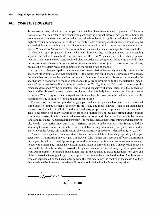
398 Digital System Design in Practice
18.1 TRANSMISSION LINES
Transmission lines, reflections, and impedance matching have been alluded to previously. The term
transmission line
can refer to any conductive path carrying a signal between two points, although itsusual meaning is in the context of a conductive path whose length is significant relative to the signal’shighest-frequency component. Circuits are normally drawn assuming ideal conductors whose lengthsare negligible and assuming that the voltage at any instant in time is constant across the entire con-ductor. When a wire “becomes a transmission line,” it means that it can no longer be considered ideal.An electrical signal propagates down a wire with finite velocity, which guarantees that a changingsignal at one end will take a finite time to reach the other end. When a signal’s rate of change is slowrelative to the wire’s delay, many nonideal characteristics can be ignored. Older digital circuits thatran at several megahertz with slow transition times were often not subject to transmission line effects,because the wire delay was short compared to the signal’s rate of change.
A signal that changes rapidly forces one end of a transmission line to a significantly different volt-age from other points along that conductor. At the instant this rapid change is produced by a driver,the signal has not yet reached the load at the end of the wire. Rather than observing current and volt-age that are in proportion to the load impedance, they are in proportion to the characteristic imped-ance of the transmission line, commonly written as Z
O
. Z
O
is not a DC load; it represents thereactance developed by the conductors’ inductive and capacitive characteristics. It is the impedancethat would be observed between the two conductors of an infinitely long transmission line at nonzerofrequency. When a high-frequency signal transitions before the driver sees the end load, it is as if thetransmission line is infinitely long at that moment in time.
Transmission lines are composed of a signal path and a return path, each of which can be modeledusing discrete lumped elements as shown in Fig. 18.1. The model shown is that of an unbalancedtransmission line wherein all of the inductive and lossy properties are represented in one conductor.This is acceptable for many transmission lines in a digital system, because printed circuit boardscommonly consist of etched wire conductors adjacent to ground planes that have negligible induc-tance and resistance. A balanced transmission line model, such as that representing a twisted pair ca-ble, would show series inductance and resistance in both conductors. Analysis is simplified byassuming lossless conductors, which is often a suitable starting point in a digital system with moder-ate wire lengths. Using this simplification, the characteristic impedance is defined as Z
O
= .Characteristic impedance is an important attribute, because it defines how a high-speed signal propa-
gates down a transmission line. A signal’s energy can fully transfer only between different transmissionline segments that have equal Z
O
. An impedance discontinuity results when two transmission lines arejoined with differing Z
O
. Impedance discontinuities result in some of a signal’s energy being reflectedback in the direction from which it arrived. This phenomenon is the crux of many signal integrity prob-lems. An improperly terminated transmission line has the potential to cause reflections from each endof the wire so that the original signal is corrupted to the point of being rendered useless. A reflection co-efficient, represented by the Greek letter gamma (
Γ
), that determines the fraction of the incident voltagethat is reflected back from an impedance discontinuity is defined in the following equation:
RP
RSL
C
FIGURE 18.1 Lumped transmission line model.
L C÷
-Balch.book Page 398 Thursday, May 15, 2003 3:46 PM

Signal Integrity 399
Gamma is a dimensionless quantity that ranges from +1 to –1 and is a function of Z
O
and the nextsegment’s impedance, Z
L
. It can be seen from this relationship that, when a transmission line is leftopen, Z
L
=
∞
and
Γ
= 1: the entire voltage is reflected back to the source. This is the default situationfor most digital signals, because a high-impedance logic input is effectively an open circuit from atransmission line perspective. Incidentally, a short-circuited transmission line, though not very desir-able for digital signals, results in
Γ
= –1, because Z
L
= 0, and causes the reflected signal to cancel theincident signal at the load. When a resistor equal to Z
O
is placed at the end of a transmission linesuch that it connects the line’s signal and return paths,
Γ
= 0, the line is said to be terminated, and noreflections are induced.
Transmission line reflections are perhaps best understood in a qualitative manner by looking at atime-domain view of a propagating signal. Figure 18.2 shows three scenarios that illustrate the bene-fits of termination and the effects of the reflection coefficient. The first scenario shows an edge in-jected into a 1 ns transmission line (about 6 in [0.15 m] long) that is improperly designed.Substantial bounce is present at the load. A high-speed clock is shown in the second scenario in-jected into the same transmission line. Note the bounce at both logic levels that can potentially cre-ate detection problems at the load. Poorly designed transmission lines can exhibit a wide variety oftroublesome transient phenomena. Some may be better or worse than what is shown here. The thirdscenario shows the same clock injected into the same transmission line but with proper termination.The signal integrity is about as good as can be expected in a real circuit. There will always be smalltransients, even when a transmission line is properly matched, because of nonideal characteristics in-cluding stray inductance and capacitance in wires and termination components.
The need to minimize impedance discontinuities in modern printed circuit boards has given riseto the concept of controlled-impedance PCB design and manufacture. When a signal path and returnpath are arranged in various topologies, Z
O
of the resultant transmission line is deterministic to anaccuracy defined by the tolerance of the dimensions and electrical properties of the PCB materials. Ifall traces on a PCB are manufactured with similar Z
O
, signals are subject to low reflection coeffi-cients as they travel throughout the board. Three of the common PCB transmission line topologiesare microstrip, symmetric stripline, and asymmetric stripline as illustrated in Fig. 18.3. These topol-ogies assume one or two continuous ground planes adjacent to each signal layer. A continuousground plane offers low sheet inductance with excellent high-frequency characteristics. Microstriptransmission lines are fabricated on the surface layers of PCBs where there is a single ground planeunderneath the surface signal layer. A symmetrical stripline is evenly suspended between the twoground planes, while an asymmetric stripline has unequal spacings. Dual asymmetric striplines areimplemented to achieve higher wiring density in a PCB versus symmetric striplines because of thehigher ratio of signal to ground plane layers. Dual striplines have the potential for interference be-tween adjacent signal layers, requiring more careful layout than with single striplines.
Z
O
is a function of the trace geometry (width and thickness) and the relative permittivity andheight of the dielectric, or insulator, that separates the ground planes from the traces. Relative per-mittivity,
ε
r
, also called the
dielectric constant,
quantifies the effect of an insulating material on thecapacitance between two conductors relative to free space. The relative permittivity of free space is 1by definition. Common insulators have
ε
r
ranging from 2 to 10. For microstrip and stripline topolo-gies, Z
O
is defined in the following equations:
*
*
IPC-2141—Controlled Impedance Circuit Boards and High-Speed Logic Design,
Institute for Interconnecting and PackagingElectronic Circuits, 1996, pp. 11–14.
ΓZL ZO–
ZL ZO+--------------------=
-Balch.book Page 399 Thursday, May 15, 2003 3:46 PM
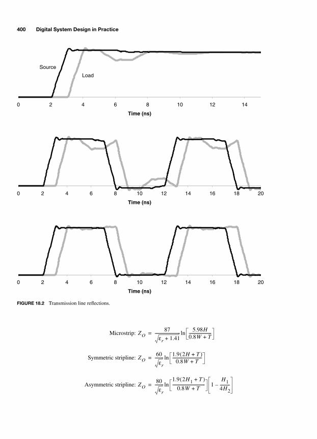
400 Digital System Design in Practice
Microstrip:
Symmetric stripline:
Asymmetric stripline:
0 2 4 6 8 10 12 14
Time (ns)
Load
Source
0 2 4 6 8 10 12 14 16 18 20
Time (ns)
0 2 4 6 8 10 12 14 16 18 20
Time (ns)
FIGURE 18.2 Transmission line reflections.
ZO87
εr 1.41+-------------------------- 5.98H
0.8W T+-----------------------ln=
ZO60
εr
--------- 1.9 2H T+( )0.8W T+
------------------------------ln=
ZO80
εr
---------1.9 2H1 T+( )
0.8W T+--------------------------------- 1
H1
4H2----------–ln=
-Balch.book Page 400 Thursday, May 15, 2003 3:46 PM
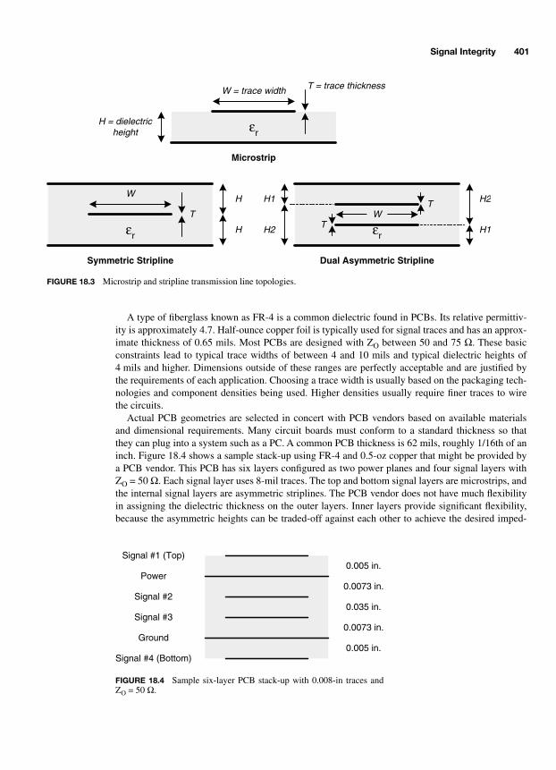
Signal Integrity 401
A type of fiberglass known as FR-4 is a common dielectric found in PCBs. Its relative permittiv-ity is approximately 4.7. Half-ounce copper foil is typically used for signal traces and has an approx-imate thickness of 0.65 mils. Most PCBs are designed with Z
O
between 50 and 75
Ω
. These basicconstraints lead to typical trace widths of between 4 and 10 mils and typical dielectric heights of4 mils and higher. Dimensions outside of these ranges are perfectly acceptable and are justified bythe requirements of each application. Choosing a trace width is usually based on the packaging tech-nologies and component densities being used. Higher densities usually require finer traces to wirethe circuits.
Actual PCB geometries are selected in concert with PCB vendors based on available materialsand dimensional requirements. Many circuit boards must conform to a standard thickness so thatthey can plug into a system such as a PC. A common PCB thickness is 62 mils, roughly 1/16th of aninch. Figure 18.4 shows a sample stack-up using FR-4 and 0.5-oz copper that might be provided bya PCB vendor. This PCB has six layers configured as two power planes and four signal layers withZ
O
= 50
Ω
. Each signal layer uses 8-mil traces. The top and bottom signal layers are microstrips, andthe internal signal layers are asymmetric striplines. The PCB vendor does not have much flexibilityin assigning the dielectric thickness on the outer layers. Inner layers provide significant flexibility,because the asymmetric heights can be traded-off against each other to achieve the desired imped-
εr
W
T
Symmetric Stripline
H
H
εr
WT
Dual Asymmetric Stripline
H1
H2
TH2
H1
εr
W = trace width
H = dielectricheight
T = trace thickness
Microstrip
FIGURE 18.3 Microstrip and stripline transmission line topologies.
Signal #1 (Top)
Signal #4 (Bottom)
Signal #2
Signal #3
Ground
Power0.005 in.
0.0073 in.
0.0073 in.
0.005 in.
0.035 in.
FIGURE 18.4 Sample six-layer PCB stack-up with 0.008-in traces andZO = 50 Ω.
-Balch.book Page 401 Thursday, May 15, 2003 3:46 PM
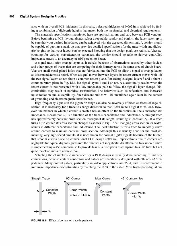
402 Digital System Design in Practice
ance with an overall PCB thickness. In this case, a desired thickness of 0.062 in is achieved by find-ing a combination of dielectric heights that match both the mechanical and electrical requirements.
The materials specifications mentioned here are approximations and vary between PCB vendors.Before beginning a PCB layout, always select a reputable vendor and confirm the layer stack-up tobe sure that your desired impedance can be achieved with the expected dimensions. A vendor shouldbe capable of quoting a stack-up that provides detailed specifications for the trace width and dielec-tric heights so that your layout can be executed knowing that the design goals are realistic. After ac-counting for various manufacturing variances, the vendor should be able to deliver controlledimpedance traces to an accuracy of
±
10 percent or better.A signal must often change layers as it travels, because of obstructions caused by other devices
and other groups of traces that are competing for their journey across the same area of circuit board.Vias are small metal-plated holes that are fabricated into the PCB to allow a signal to change layersas it is routed across a board. When a signal moves between layers, its return current moves with it ifthe two signal layers do not share a common return plane. For example, signal layers 3 and 4 share acommon return plane in Fig. 18.4, but signal layers 1 and 4 do not. A discontinuity results when thereturn current is not presented with a low-impedance path to follow the signal’s layer change. Dis-continuities may result in nonideal transmission line behavior, such as reflections and increasednoise radiation and susceptibility. Such discontinuities will be mentioned again later in the contextof grounding and electromagnetic interference.
High-frequency signals in the gigahertz range can also be adversely affected as traces change di-rection. It is necessary for a trace to change direction so that it can route a signal to its load. How-ever, the manner in which a corner is created has an effect on the transmission line’s characteristicimpedance. Recall that Z
O
is a function of the trace’s capacitance and inductance. A straight tracehas approximately constant cross section throughout its length, resulting in constant Z
O
. If a traceturns a 90° corner, its cross section changes as shown in Fig. 18.5. Changing cross section, or width,results in different capacitance and inductance. The ideal situation is for a trace to smoothly curvearound corners to maintain constant cross section. Although this is usually done for the most de-manding very high-speed circuits, it is uncommon for normal digital signals because of the burdenthat smooth curves place on conventional PCB design software. Imperfections due to corners arenegligible for typical digital signals into the hundreds of megahertz. An alternative to a smooth curveis implementing a 45° compromise to provide less of a disruption as compared to a 90° turn, but notquite the cleanliness of a true curve.
Selecting the characteristic impedance for a PCB design is usually done according to industryconventions, because certain connectors and cables are specifically designed with 50- or 75-
Ω
im-pedances. Many coaxial cables, particularly in video applications, are 75
Ω,
and it is convenient tominimize impedance discontinuities by matching the PCB to the cable. Most high-speed digital cir-
ConstantWidth
Straight Trace 90° Corner
Corner Width
= W 2 ≈1.4 W
W
Ideal Curve
ConstantWidth
45° Compromise
Corner Width≈1.1 W
FIGURE 18.5 Effect of corners on trace impedance.
-Balch.book Page 402 Thursday, May 15, 2003 3:46 PM

Signal Integrity 403
cuits use 50-
Ω
transmission lines, and some connectors are available with this impedance as well.There are advantages and disadvantages in using higher- or lower-impedance transmission lines. Alower-impedance transmission line requires a thinner dielectric between the signal and return paths.This smaller gap makes the transmission line less susceptible to radiating and coupling noise. It alsoallows multilayer circuit boards to be made thinner. The disadvantage of lower-impedance transmis-sion lines is that they require higher drive current. Most ICs are capable of driving 50-
Ω
transmis-sion lines, and high-speed design makes the trade-off of improved noise immunity worth the addedpower consumption. However, slower circuits may be more suited to 75-
Ω
transmission lines forpower savings.
18.2 TERMINATION
In applying transmission line theory to a digital signal, one should first determine whether the com-bination of signal transition speed and wire length combine to merit transmission line analysis. Dig-ital signals are characterized not only by their repetitive frequency but also by the frequencycomponents in their edges. A signal with a rapid transition time will have high-frequency compo-nents regardless of how long the repetition period. Rules of thumb vary, but a common referencepoint is to treat a wire as a transmission line if the signal’s rise time is less than four times the prop-agation delay of the wire. The common definition of rise time is the time that the signal takes to tran-sition from 10 to 90 percent of its full amplitude. If the signal transitions slowly with respect to thewire delay, it can be assumed that all points on the wire transition together as the applied signal tran-sitions. When a signal transitions quickly and the wire is long relative to this time, the wire should betreated as a transmission line. It is now common to see signals that transition in 1 ns, meaning thatwires with propagation delays greater than 250 ps (about 1.5 in, or 38 mm) require transmission lineanalysis!
There are several basic termination schemes and numerous variant schemes that have been de-signed for special digital signaling standards. From our previous discussion of the reflection coeffi-cient, the first obvious termination scheme is to place a resistor equal to Z
O
at the end of atransmission line as shown in Fig. 18.6. This is known as
parallel termination
. Note that a transmis-sion line is identified using a graphical representation of a coaxial cable. This does not mean that atransmission line must be implemented as such, but it conveys the idea that the wire length is non-negligible and cannot be treated as a single node of constant voltage as other wires are. A ground isexplicitly connected to the transmission line return path to clearly indicate the circuit’s return path.Assuming ideal conditions where Z
O
is exactly known, R = Z
O
, the output impedance of the driver is0
Ω
, and there is no stray capacitance or inductance at either end of the transmission line, paralleltermination yields
Γ
= 0, and no reflections are present. Of course, these ideal conditions are neverachieved, and real terminated transmission lines have some degree of imperfection. The goal is not
ZO = 50 Ω
50 Ω
FIGURE 18.6 Parallel termination.
-Balch.book Page 403 Thursday, May 15, 2003 3:46 PM

404 Digital System Design in Practice
to accomplish the impossible but to achieve a transmission line topology in which the reflections aresmall enough to not degrade the load’s valid detection of logic-1 and logic-0 states.
Parallel termination resistors should always be placed as close to the end of a transmission lineas possible to minimize stub lengths between the terminator and the IC pin. Stubs appear as trans-mission lines of their own and can cause more reflections if not kept short. It can be difficult tosqueeze termination components close to IC pins, but efforts should be made to achieve the bestpractical results.
Terminating a line at one end as shown in Fig. 18.6 is proper for a unidirectional signal, becausethe driver launches a signal into one end of the transmission line, and the termination is placed at theload end to prevent reflections. When both ends of the line are driven, as is the case with bidirec-tional buses, both ends require termination. The resistor at the driver end appears as a normal DCload, and the resistor at the far end serves as a terminator.
Situations commonly arise in which a bus has more than one load. A microprocessor bus musttypically connect to several memory and peripheral ICs. The transmission line topology must be laidout carefully to minimize the potential for harmful reflections. The best scenario is to create a single,continuous transmission line terminated at each end that snakes through the circuit board and con-tacts each IC so that the stubs to each IC are of negligible length as shown in Fig. 18.7. When an ICat either end drives the bus, it drives a single transmission line that is terminated at the other end.When an IC in the middle drives the bus, it drives two equivalent transmission lines that are termi-nated at their ends. Graphically, the single transmission line can be drawn as shown using multiplesegments connected by nodes that indicate tap points for individual ICs. Because nodes are drawnwith the assumption of negligible length and constant voltage, they are conceptually transparent tothe transmission line segments on each side. Keep in mind that not all buses require a perfect trans-mission line topology. Depending on their wire lengths and the switching times of the drivers, thewires may be regarded as idealized and not require special handling.
Many nonideal topologies exist in which no attempt has been made to shorten stubs and there isreally no identifiable transmission line “backbone.” Instead, the wiring is fairly random. A topologylike this works either by virtue of the fact that the signal transition times are slow enough to not
ZO
IC
IC
ZO
ICZO
IC
ZO
ZO
FIGURE 18.7 Multidrop transmission line topology.
-Balch.book Page 404 Thursday, May 15, 2003 3:46 PM

Signal Integrity 405
make transmission line effects significant, or by plain luck. If the former, the circuit is perfectlyvalid, because there is no reason to cause wiring headaches if a wire does not have to be regarded asa transmission line. If the latter, luck can turn at any time with slight variations in components. Thisoften explains why one or two units work in the lab, but a small manufacturing run has a high per-centage of failures.
Parallel termination has the unfortunate consequence of heavily loading a driver because it is, af-ter all, a small resistance connected directly across the signal and return paths. The driver sees a loadof Z
O
when it begins to switch its output but, once the line has stabilized, it still sees a load of R =Z
O
. This is a substantial load with a 50- or 75-
Ω
transmission line. A 3.3-V driver would have todrive 66 mA into a 50-
Ω
load. If many bus signals need to be terminated, the power dissipation andstress on the driver ICs quickly mounts. This situation gets worse when terminating both ends of abidirectional line.
There are several variants of parallel termination that seek to minimize the DC current drawn bythe termination resistors.
Thevenin
, or
split termination,
operates using two resistors, each of whichis chosen to be twice Z
O
as shown in Fig. 18.8. One resistor terminates to ground and the other to thepositive voltage rail. From an AC perspective, the positive voltage rail acts as a ground, and the par-allel resistor combination appears as a single resistor equivalent of Z
O
connected to ground. Thebenefit of split termination is that the maximum DC current drawn from the driver is halved, becausea 100-
Ω
load is observed to the opposing voltage rail. When the driver drives to V
DD
, the 100-
Ω
re-sistor to ground is the only load with a DC voltage drop across it. Split termination’s disadvantage isthat it always dissipates power, because the resistors establish a DC path between V
DD
and ground.The Thevenin concept can be carried further by employing a dedicated termination voltage rail,
V
TT
, that equals V
DD
÷
2 and terminating to this rail using a resistor equal to Z
O
as shown in Fig.18.9. This scheme provides equivalent termination with less power dissipation, because the maxi-mum voltage drop is V
DD
÷
2 instead of V
DD
. An additional benefit is that the terminator only dissi-pates power when the line is active. Bidirectional buses that are released to high-impedance statesduring idle will not load the termination resistor during that idle time.
Another variant of parallel termination uses a capacitor in series with the resistor to reduce powerdissipation and is shown in Fig. 18.10.
AC termination
is suitable for clock signals or other DC bal-anced signals (e.g., 8B10B encoded signals), because such signals allow the capacitor to charge toV
DD ÷ 2 with the resultant benefits of reduced power dissipation as seen with VDD ÷ 2 termination.Unbalanced signals remain at a static voltage for too long and charge the capacitor to either voltagerail. When a transition finally occurs, the full VDD voltage drop appears across the terminator in aconceptually identical arrangement to basic parallel termination. The capacitor value must be chosenso that it maintains a nearly constant voltage during the balanced signal’s period. A common 0.1-µF
100 Ω
100 Ω
VDD
ZO = 50 Ω
FIGURE 18.8 Thevenin termination.
-Balch.book Page 405 Thursday, May 15, 2003 3:46 PM
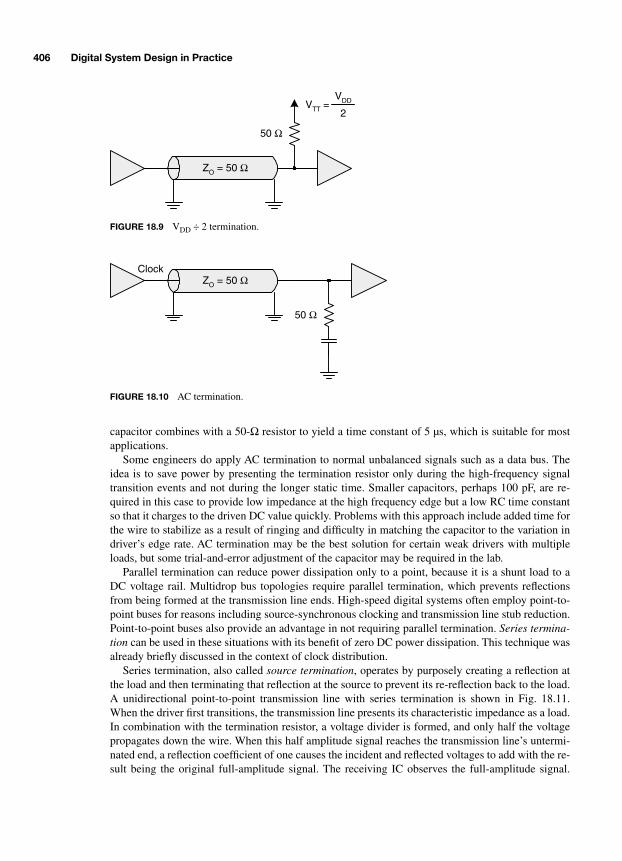
406 Digital System Design in Practice
capacitor combines with a 50-Ω resistor to yield a time constant of 5 µs, which is suitable for mostapplications.
Some engineers do apply AC termination to normal unbalanced signals such as a data bus. Theidea is to save power by presenting the termination resistor only during the high-frequency signaltransition events and not during the longer static time. Smaller capacitors, perhaps 100 pF, are re-quired in this case to provide low impedance at the high frequency edge but a low RC time constantso that it charges to the driven DC value quickly. Problems with this approach include added time forthe wire to stabilize as a result of ringing and difficulty in matching the capacitor to the variation indriver’s edge rate. AC termination may be the best solution for certain weak drivers with multipleloads, but some trial-and-error adjustment of the capacitor may be required in the lab.
Parallel termination can reduce power dissipation only to a point, because it is a shunt load to aDC voltage rail. Multidrop bus topologies require parallel termination, which prevents reflectionsfrom being formed at the transmission line ends. High-speed digital systems often employ point-to-point buses for reasons including source-synchronous clocking and transmission line stub reduction.Point-to-point buses also provide an advantage in not requiring parallel termination. Series termina-tion can be used in these situations with its benefit of zero DC power dissipation. This technique wasalready briefly discussed in the context of clock distribution.
Series termination, also called source termination, operates by purposely creating a reflection atthe load and then terminating that reflection at the source to prevent its re-reflection back to the load.A unidirectional point-to-point transmission line with series termination is shown in Fig. 18.11.When the driver first transitions, the transmission line presents its characteristic impedance as a load.In combination with the termination resistor, a voltage divider is formed, and only half the voltagepropagates down the wire. When this half amplitude signal reaches the transmission line’s untermi-nated end, a reflection coefficient of one causes the incident and reflected voltages to add with the re-sult being the original full-amplitude signal. The receiving IC observes the full-amplitude signal.
50 Ω
VTT = 2
VDD
ZO = 50 Ω
FIGURE 18.9 VDD ÷ 2 termination.
50 Ω
ClockZO = 50 Ω
FIGURE 18.10 AC termination.
-Balch.book Page 406 Thursday, May 15, 2003 3:46 PM
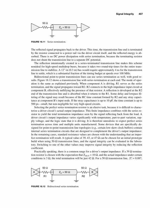
Signal Integrity 407
The reflected signal propagates back to the driver. This time, the transmission line end is terminatedby the resistor connected to a power rail via the driver circuit itself, and the reflected energy is ab-sorbed. There is no DC power dissipation with series termination, because the terminating resistordoes not shunt the transmission line to a separate DC potential.
The reflection intentionally created in a series-terminated transmission line makes this schemenonideal for high-speed multidrop buses, because it takes two round-trip times for the entire trans-mission line to stabilize. A 12”-in (0.3 m) bus would require approximately 4 ns for the transmissionline to settle, which is a substantial fraction of the timing budget at speeds over 100 MHz.
Bidirectional point-to-point transmission lines can use series termination as well, with good re-sults. Figure 18.12 shows a transmission line with series termination at each end. The mode of oper-ation is the same as explained previously. When component A is driving, R1 serves as the seriestermination, and the signal propagates toward R2. R2 connects to the high-impedance input circuit atcomponent B, effectively nullifying the presence of that resistor. A reflection is developed at the R2end of the transmission line and is absorbed when it returns to the R1. Some delay and lowpass fil-tering of the signal may result because of the RC time constant formed by R2 and any stray capaci-tance at component B’s input node. If the stray capacitance is up to 10 pF, the time constant is up to500 ps—small, but non-negligible for very high-speed circuits.
Selecting the perfect series termination resistor is an elusive task, because it is difficult to charac-terize a driver circuit’s actual output impedance. This finite impedance combines with the series re-sistor to yield the total termination impedance seen by the signal reflecting back from the load. Adriver circuit’s output impedance varies significantly with temperature, part-to-part variation, sup-ply voltage, and the logic state that it is driving. It is therefore unrealistic to expect perfect seriestermination across time and multiple units manufactured. Some devices that are specifically de-signed for point-to-point transmission line topologies (e.g., certain low-skew clock buffers) containinternal series termination circuits that are designed to complement the driver’s output impedance.In the remaining cases, standard resistance values are chosen with the understanding that an imper-fect termination will result. A typical value of 39, 43, or 47 Ω can be chosen for an initial prototypebuild when using 50-Ω transmission lines, and the signal integrity can be evaluated in the labora-tory. Switching to one of the other values may improve signal integrity by reducing the reflectioncoefficient.
Practically speaking, there is a common range for a driver’s output impedance. If a 39 Ω termina-tion resistor is chosen with the expectation that ZOUT = 10 Ω, and the actual impedance under certainconditions is 3 Ω, the total termination will be just 42 Ω. For a 50 Ω transmission line, = 0.087,
50 Ω
ZO = 50 Ω
FIGURE 18.11 Series termination.
50 Ω 50 Ω
R1 R2
A BZO = 50 Ω
FIGURE 18.12 Bidirectional series termination.
Γ
-Balch.book Page 407 Thursday, May 15, 2003 3:46 PM
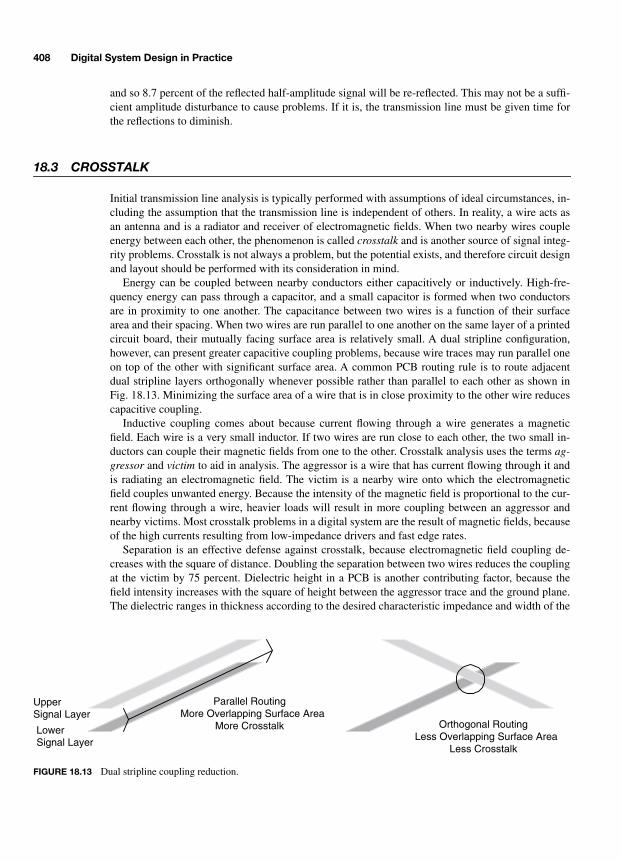
408 Digital System Design in Practice
and so 8.7 percent of the reflected half-amplitude signal will be re-reflected. This may not be a suffi-cient amplitude disturbance to cause problems. If it is, the transmission line must be given time forthe reflections to diminish.
18.3 CROSSTALK
Initial transmission line analysis is typically performed with assumptions of ideal circumstances, in-cluding the assumption that the transmission line is independent of others. In reality, a wire acts asan antenna and is a radiator and receiver of electromagnetic fields. When two nearby wires coupleenergy between each other, the phenomenon is called crosstalk and is another source of signal integ-rity problems. Crosstalk is not always a problem, but the potential exists, and therefore circuit designand layout should be performed with its consideration in mind.
Energy can be coupled between nearby conductors either capacitively or inductively. High-fre-quency energy can pass through a capacitor, and a small capacitor is formed when two conductorsare in proximity to one another. The capacitance between two wires is a function of their surfacearea and their spacing. When two wires are run parallel to one another on the same layer of a printedcircuit board, their mutually facing surface area is relatively small. A dual stripline configuration,however, can present greater capacitive coupling problems, because wire traces may run parallel oneon top of the other with significant surface area. A common PCB routing rule is to route adjacentdual stripline layers orthogonally whenever possible rather than parallel to each other as shown inFig. 18.13. Minimizing the surface area of a wire that is in close proximity to the other wire reducescapacitive coupling.
Inductive coupling comes about because current flowing through a wire generates a magneticfield. Each wire is a very small inductor. If two wires are run close to each other, the two small in-ductors can couple their magnetic fields from one to the other. Crosstalk analysis uses the terms ag-gressor and victim to aid in analysis. The aggressor is a wire that has current flowing through it andis radiating an electromagnetic field. The victim is a nearby wire onto which the electromagneticfield couples unwanted energy. Because the intensity of the magnetic field is proportional to the cur-rent flowing through a wire, heavier loads will result in more coupling between an aggressor andnearby victims. Most crosstalk problems in a digital system are the result of magnetic fields, becauseof the high currents resulting from low-impedance drivers and fast edge rates.
Separation is an effective defense against crosstalk, because electromagnetic field coupling de-creases with the square of distance. Doubling the separation between two wires reduces the couplingat the victim by 75 percent. Dielectric height in a PCB is another contributing factor, because thefield intensity increases with the square of height between the aggressor trace and the ground plane.The dielectric ranges in thickness according to the desired characteristic impedance and width of the
Upper Signal Layer
Lower Signal Layer
Parallel RoutingMore Overlapping Surface Area
More Crosstalk Orthogonal RoutingLess Overlapping Surface Area
Less Crosstalk
FIGURE 18.13 Dual stripline coupling reduction.
-Balch.book Page 408 Thursday, May 15, 2003 3:46 PM
Signal Integrity 409
copper traces. As the dielectric gets thinner, the capacitance between the trace and ground plane in-creases, thereby decreasing ZO. The trace’s inductance must be increased to compensate for this de-creased capacitance, indicating that a trace must be narrower to achieve 75 Ω versus 50 Ω with acertain dielectric height. Put another way, a 50-Ω transmission line has a lower dielectric height for agiven trace width and, hence, weaker fields to cause crosstalk.
Crosstalk is a three-dimensional problem, and length is the third variable in coupling energy ontoa victim trace. Traces that run parallel to each other are parallel antennas. Longer antennas can cou-ple more energy. Therefore, many high-speed PCB designs enforce maximum parallelism rules thatdefine the maximum distance that is allowable for two traces to run parallel to each other. Parallel-ism rules are related to separation rules. Traces that are spaced farther apart can tolerate longer par-allel runs, because the separation reduces the aggressor’s radiated field strength.
It is difficult to make generalizations about separation and parallelism rules, because every situa-tion is unique. Furthermore, the formulas that define field strength and coupling coefficients arecomplex functions that incorporate dimensional and material parameters. A detailed crosstalk analy-sis requires the use of specialized software that simulates the coupling phenomena using detailedmathematical models of the driver and load circuits, the circuit board materials, and the three-dimen-sional arrangement of multiple traces. Such programs are known as field solvers and are availablefrom a variety of vendors including Ansoft, Cadence, Innoveda, and Mentor Graphics.
When engineers do not have field-solving software at their disposal, very conservative design rulesare often used to minimize the probability of excessive crosstalk. Sensitive signals are spaced apartfrom others. Parallelism is limited for signals whose spacing approaches the dielectric height wherefield coupling is greater. These rules are very coarse approximations, and application-specific rulesneed to be applied for very high-speed designs to avoid potentially thorny signal integrity problems inthe prototype. If a great deal of time and money are invested in designing a leading-edge high-speedsystem, it is prudent to invest some time and money in appropriate signal integrity analysis tools.
One saving grace when dealing with crosstalk is that many signals do not have to be protectedfrom each other if it can be shown that noise caused by crosstalk will not affect the received signal.Consider the case of a microprocessor bus’s individual wires that are traveling close together be-tween ICs. Inductive coupling, which is the dominant crosstalk contributor, occurs when current isflowing, because the magnetic field is proportional to current flow. Significant current flows duringthe switching time of the digital signal. Once the signal has stabilized, the load presents the driverwith high impedance. This means that crosstalk between signals that transition together occursmainly while they are switching and then quiets down after the lines have stabilized. A properly de-signed system does not sample signals until they have safely stabilized, at which point crosstalkwithin the group becomes negligible.
The wires that compose a single bus can usually be routed in close proximity to each other with-out regard for crosstalk within the bus. Clocks require special consideration, because one does notwant a great deal of noise from switching bus wires to couple onto the clock wire and cause a falseedge to appear. Likewise, the clock’s transitions can potentially couple onto data wires and cause anincorrect observation at the receiver. Clocks are usually given preferential routing treatment asidefrom their low-skew distribution requirement. Clock traces are often routed before all others, andstricter minimum spacing rules may be used to minimize corruption of clock signals. Very conserva-tive systems are designed by dedicating one or more entire PCB signal layers to clock routing so thatthe clocks can enjoy substantial trace-to-trace spacing minimums.
Although signals within a bus are usually not sensitive to mutual crosstalk, signals that transitionasynchronously with respect to each other are prime candidates for trouble. Asynchronous signals,by definition, transition relative to each other without a defined timing relationship. If a system hastwo buses on different clock domains whose wires are mixed in close proximity with long parallelruns, it is probable that one bus will often transition during the assumed stable time of the other bus
-Balch.book Page 409 Thursday, May 15, 2003 3:46 PM

410 Digital System Design in Practice
just as it is being sampled. Attention should be paid to the routing of asynchronous signals by sepa-rating them and minimizing parallelism.
18.4 ELECTROMAGNETIC INTERFERENCE
Electromagnetic interference (EMI) and crosstalk are closely related topics. It has already been seenthat the quality and proximity of a ground plane has a significant impact on a transmission line andthe fields that it radiates. Magnetic field strength is proportional to current and is also a function ofthe loop area defined by the conductors carrying that current. All circuits are loops, because currentcannot flow unless a complete loop is formed from the source, through the load, and back to thesource. Digital circuits are no exception to this rule, despite inputs typically having high impedanceand low DC input currents. A high-speed system moves substantial currents around many individualloops formed by digital buses because of the rapid charging and discharging of transmission linesand input nodes. Even though each bit in a data bus may not be drawn with an explicit return pathshown, that return path must exist for the circuit to function.
As the size of the loop formed by the signal’s source and return paths increases, that wire radiatesa magnetic field of greater strength and is more susceptible to picking up ambient magnetic fields.The general term for a circuit’s sensitivity to coupling electromagnetic fields is EMI susceptibility. Acircuit forms a loop antenna, and a loop antenna is more efficient with increasing area. Loop areaand its effect on crosstalk have already been touched on in terms of dielectric height in a PCB. Asthe signal wire is brought closer to the ground plane, as it is in a lower-impedance design, the looparea and field strength decrease as illustrated in Fig. 18.14.
Minimizing loop area is a key reason why solid ground planes are necessary to high-speed sig-nals. Consider the two scenarios, with and without ground planes, in Fig. 18.15. A ground plane al-lows a high-speed return current to flow through a path of least inductance that is directly under thesignal trace. If the ground plane is replaced by a few discrete wires, those wires cannot lie directlyunder all signal paths. The return current is forced to take a path that is a greater physical distancefrom the signal path, with an associated increase in loop area and EMI susceptibility.
Vias along a set of PCB traces can inadvertently create larger loops. When a signal moves be-tween PCB layers, its return current must follow. If a signal changes layers that are on opposite sidesof the same ground plane, the return current is able to follow without interruption. Signals oftenmove between layers that do not share the same return plane. In these cases, the return current findsthe lowest-impedance path to the return plane that is adjacent to the new signal layer. This path maybe direct, capacitive, or a combination of the two. If the new return plane is at the same DC level asthe current plane (e.g., two different ground planes), the path of least impedance may be directlythrough a nearby via that connects the planes. If the new return plane is at a different DC level (e.g.,a power plane serves as an AC ground), the return current capacitively couples between planes. Evenif the planes share the same DC level, capacitive coupling may be the path of least impedance.
Ground Plane
Signal Trace
DielectricHeight
Loop Area
Ground Plane
Signal Trace
DielectricHeight
Loop Area
FIGURE 18.14 Loop area vs. PCB dielectric height.
-Balch.book Page 410 Thursday, May 15, 2003 3:46 PM

Signal Integrity 411
Capacitive coupling can occur through bypass capacitors that connect the two return planes andthrough interplane capacitance that is a function of the PCB dimensions and materials. Low-induc-tance capacitors are critical to provide adequate high-frequency coupling between planes. Imped-ance is a product of inductance and frequency. A bypass capacitor’s total circuit inductance is thesum of the capacitor’s inherent inductance and additional inductance caused by PCB traces and viasthat connect it to the return planes. Typical surface mount capacitors in 0603 or similar packages canexhibit total inductance of approximately 2 to 3 nH. This inductance, combined with typical capaci-tance values of 0.1 or 0.01 µF, allow an impedance calculation at a given frequency. When multiplebypass capacitors are in close proximity to a via, they form a parallel combination with lower totalinductance and higher total capacitance—both of which are desirable characteristics. The closer thebypass capacitors are to a via in question, the smaller the loop that is created for high-frequency re-turn current between two planes. Nearby capacitors improve the high-frequency characteristics ofthe transmission line, whereas more distant capacitors increase the circuit’s EMI susceptibility.
Discrete bypass capacitors are often the path of least impedance between return planes. As operat-ing frequencies rise, however, the finite inductance of discrete components becomes more of a prob-lem. A PCB may be constructed with planes separated by very thin dielectrics to provide significantinterplane capacitance with negligible inductance. Capacitance increases with decreasing spacingbetween planes, and inductance decreases with greater surface area that a plane offers. High-fre-quency systems may require such construction techniques to function properly. These techniquescan increase system cost by requiring more expensive thin dielectric materials and a greater numberof PCB layers. Such costs are among many complexities involved in creating high-performance sys-tems and must be considered when deciding on the practicality of a design.
The potential for via-induced EMI problems always exists. Conservative designs attempt to routesensitive and very high-speed signals with a minimum number of vias to reduce ground discontinu-ity problems. When vias are necessary, it is best to switch only between pairs of signal layers that areon opposite sides of the same ground plane.
Return path discontinuities may also be caused by breaks in power and ground planes. A PCBmay contain multiple DC voltages (e.g., 5 and 3.3 V) on the same power plane to save money. Dif-
Driver IC
Ground Pin
Signal Pin
Receiver IC
Ground Pin
Signal Pin
Ground Plane
Minimum loop area with ground plane
Driver IC
Ground Pin
Signal Pin
Receiver IC
Ground Pin
Signal Pin
Ground Wire
Greater loop area with discrete ground wire
Loop
Loop
Signal Trace
Signal Trace
FIGURE 18.15 Greater loop circuit area without ground plane.
-Balch.book Page 411 Thursday, May 15, 2003 3:46 PM
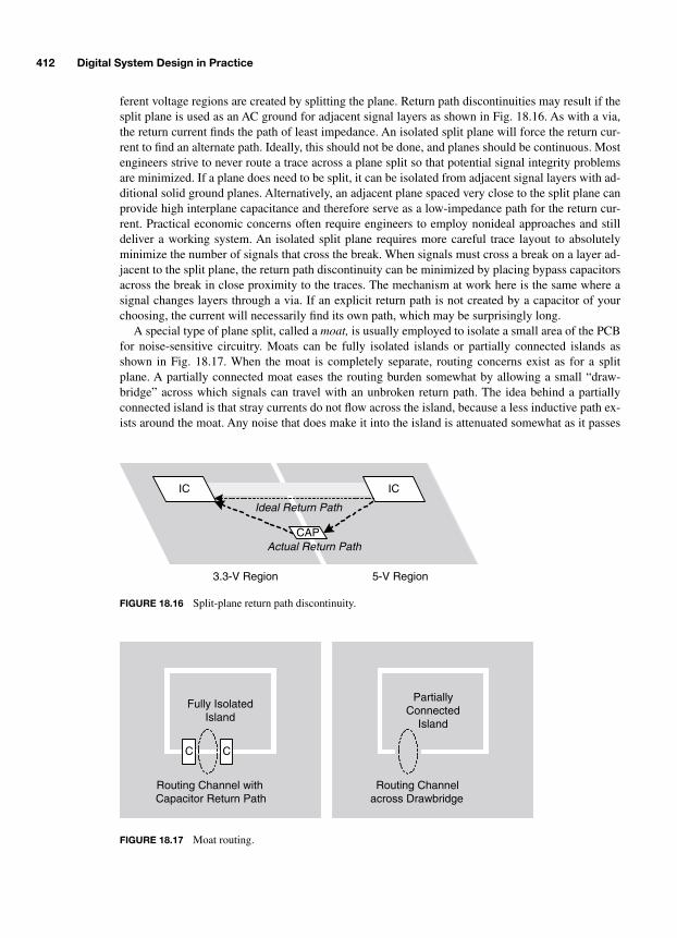
412 Digital System Design in Practice
ferent voltage regions are created by splitting the plane. Return path discontinuities may result if thesplit plane is used as an AC ground for adjacent signal layers as shown in Fig. 18.16. As with a via,the return current finds the path of least impedance. An isolated split plane will force the return cur-rent to find an alternate path. Ideally, this should not be done, and planes should be continuous. Mostengineers strive to never route a trace across a plane split so that potential signal integrity problemsare minimized. If a plane does need to be split, it can be isolated from adjacent signal layers with ad-ditional solid ground planes. Alternatively, an adjacent plane spaced very close to the split plane canprovide high interplane capacitance and therefore serve as a low-impedance path for the return cur-rent. Practical economic concerns often require engineers to employ nonideal approaches and stilldeliver a working system. An isolated split plane requires more careful trace layout to absolutelyminimize the number of signals that cross the break. When signals must cross a break on a layer ad-jacent to the split plane, the return path discontinuity can be minimized by placing bypass capacitorsacross the break in close proximity to the traces. The mechanism at work here is the same where asignal changes layers through a via. If an explicit return path is not created by a capacitor of yourchoosing, the current will necessarily find its own path, which may be surprisingly long.
A special type of plane split, called a moat, is usually employed to isolate a small area of the PCBfor noise-sensitive circuitry. Moats can be fully isolated islands or partially connected islands asshown in Fig. 18.17. When the moat is completely separate, routing concerns exist as for a splitplane. A partially connected moat eases the routing burden somewhat by allowing a small “draw-bridge” across which signals can travel with an unbroken return path. The idea behind a partiallyconnected island is that stray currents do not flow across the island, because a less inductive path ex-ists around the moat. Any noise that does make it into the island is attenuated somewhat as it passes
3.3-V Region 5-V Region
IC IC
CAP
Ideal Return Path
Actual Return Path
FIGURE 18.16 Split-plane return path discontinuity.
Fully IsolatedIsland
C C
Routing Channel withCapacitor Return Path
PartiallyConnected
Island
Routing Channelacross Drawbridge
FIGURE 18.17 Moat routing.
-Balch.book Page 412 Thursday, May 15, 2003 3:46 PM

Signal Integrity 413
through the thin drawbridge. A fully isolated island requires power and ground to be suppliedthrough passive filters or some other connection.
Remember that a key goal in designing for signal integrity is to minimize loop area and returnpath discontinuities so that less energy is radiated from a wire when it is driven, and less energy ispicked up as noise when other wires in the system are being driven.
18.5 GROUNDING AND ELECTROMAGNETIC COMPATIBILITY
By now it should be clear that grounding is a critical aspect of system design. Grounding becomesmore important as speeds increase, because more intense electromagnetic fields are present, andhigher frequencies radiate more efficiently from smaller antennas. Electromagnetic compatibility(EMC) is the ability of a system to peacefully coexist with other systems so that it neither malfunc-tions because of excessive EMI susceptibility nor causes other systems to malfunction as a result ofexcessive electromagnetic field radiation. In most situations, EMC means being a good neighbor andcomplying with governmental regulations on how much electromagnetic energy an electronic sys-tem can radiate. The Federal Communications Commission governs such regulations in the UnitedStates. Most digital systems applications are not particularly sensitive to ambient electromagneticenergy. The chances are pretty low that a computer will malfunction during normal use because ofexcessive ambient fields. Of course, this does not hold true in some demanding applications such asaerospace and military electronics.
Our discussion is concerned with basic techniques for reducing a system’s radiated electromag-netic emissions in the context of complying with government regulations. EMI reduction throughminimizing loop area and removing return path discontinuities is a fundamental starting point forEMC. Reasonable steps should be taken up front to minimize the energy that a circuit board radiates.If a sloppy design radiates significant energy, it may be difficult or impossible to effectively containthese fields to the point of regulatory compliance.
Electromagnetic energy can escape from a circuit board by radiating into space or conductingonto a cable. Radiated emissions can be blocked by enclosing the circuit board in a grounded metalenclosure. This is why many computers and other electronic equipment have metal chassis, eventhough the metal may be hidden under a plastic frame or bezel. Most metal enclosures are not per-fect closed surfaces, because slots and holes are necessary for cables, switches, airflow, and so on.Enclosures also must be assembled and are often opened for service, so there are numerous seams,hinges, and joints that connect one sheet of metal to another. All openings in the metal are potentialleakage points for radiation, depending on their size. A hole forms a slot antenna whose efficiency isa function of its size and the wavelength, λ, of energy being radiated. When engineers construct an-tennas, λ ÷ 4 and λ ÷ 2 are typical dimensions that radiate most efficiently. Clearly, slots and holeswhose largest dimensions approach λ ÷ 4 are undesirable. Limiting chassis openings to be substan-tially smaller than λ ÷ 4, perhaps λ ÷ 20, is necessary.
Keep in mind that the frequencies that must be shielded are not just the highest system clock fre-quencies but also higher-order harmonics determined by the Fourier representation of a square wave.It is not uncommon to find energy violating emissions limits at the eleventh, thirteenth, or fifteenthharmonic of a digital clock. Therefore, it is best to make openings as small as possible. A rough start-ing point might be the assumption that, for a typical system, harmonics above 1 GHz will not bestrong enough to cause problems. This may or may not be true, depending on the specific circum-stance. The wavelength corresponding to 1 GHz in free space is 30 cm, and λ ÷ 20 = 1.5 cm, or about0.6 in (1.5 cm). It is not as difficult as it may first appear to keep all openings smaller than that. Gapsfor airflow are easily implemented using fine grilles formed in the sheet metal with holes far smallerthan 0.6 in. Notice the grilles on computers, microwave ovens, and consumer electronics products.
-Balch.book Page 413 Thursday, May 15, 2003 3:46 PM

414 Digital System Design in Practice
The most troublesome gaps that cause EMC problems are improperly grounded connector shellsand poorly fitted seams between metal surfaces. Many connectors are available with metal bodies ormetal shields around plastic bodies. If these metal surfaces are securely mounted to the metal chassisat multiple points such that openings are substantially smaller than λ ÷ 4, there should be no gap atthe connector to allow excessive radiation. Seams between individual sheets of metal, either mov-able or fixed panels, must be designed to meet cleanly without the slightest buckling. Imperceptiblebuckling at seams opens gaps that radiate unwanted energy. A well designed sheet metal chassisshould have all of its fixed panels adequately riveted or welded to ensure uniform contact across theseam. Movable panels almost always require additional assistance in the form of conductive gasketsand springs. A gasket or spring serves as a flexible conductor that closes any electrical gaps betweentwo metal surfaces that move over time and that may expand and contract with temperature changes.Gasketing is directly akin to the rubber washer in a sink faucet—minute gaps must be closed to pre-vent leakage.
Plastic enclosures can also be shielded by applying conductive coatings, although this is usuallymore expensive than a sheet metal chassis, which is a reason why many products use metal ratherthan all-plastic enclosures. Many small electronic products can get away with less expensive, moreattractive, and lighter uncoated plastic packaging, because their circuits do not radiate excessive en-ergy. This may be because of their relatively slow signals, careful circuit design, or a combination ofboth.
Unwanted high-frequency noise that may be conducted onto exterior cables should be filtered be-tween the active circuitry and the cable connector. Passive differential and common-mode filters arediscussed earlier in this book. High-frequency data interfaces often have standard means of dealingwith noise, including application-specific off-the-shelf transformers and common-mode chokes.Lower-frequency interfaces such as RS-232 may be effectively filtered with a second-order LC filterusing either a choke or ferrite bead for the inductive element. If noise is still able to couple onto in-ternal wiring harnesses that lead outside the enclosure, the weapon of last resort may be a ferritecore. Ferrite cores are available in clamshell types whereby the ferrite fits around a cable, and in ringforms whereby the cable is wrapped several turns around the core. The ferrite increases the induc-tance of the cable, which increases its attenuation of high frequencies. When you see a computermonitor cable or some other type of cable that has a noticeable round bulge near one end, a clam-shell ferrite has been added, because the equipment was unable to pass emissions regulations with-out it.
Filters can also be employed to attenuate higher-order harmonics of digital signals as they are dis-tributed on the circuit board to reduce the strength of ambient electromagnetic fields on the boardand within the enclosure. Clock distribution can account for a substantial fraction of unwanted emis-sions, especially at higher-order harmonics that radiate through small metal gaps. One technique isto insert lowpass filters at clock buffer outputs to attenuate energy beyond the fifth harmonic. Asquare wave substantially retains its characteristics with only the first, third, and fifth harmonicspresent. Unfortunately, component variation, mainly in capacitors, across the individual filters on alow-skew clock tree can introduce unwanted skew at the loads. Instead of an LC or RC filter at thesource, inserting just a ferrite bead may provide sufficient high-frequency attenuation to substan-tially quiet a system. If it is unclear whether such filtering is necessary, the design can include ferritebeads as an option. Ferrite bead PCB footprints can be placed at each output of a clock driver in veryclose proximity to any series termination resistors that might already be in the design. If the ferritesare not needed, they can be substituted with 0-Ω resistors. Introduction of an extra 0-Ω resistor veryclose to the clock driver should not cause problems in most systems. For truly conservative situa-tions, these scenarios can be modeled ahead of time with field-solver software.
The method by which a system’s many ground nodes are connected has a major impact on EMCin terms of noise radiating from cables leaving the chassis. Conceptually, there is a single ground
-Balch.book Page 414 Thursday, May 15, 2003 3:46 PM

Signal Integrity 415
node that all circuits use as their reference. This is easy to achieve at DC, because resistance is thedominant characteristic that causes voltage drops, and solid sheets of metal have very low sheet re-sistances. Additionally, there are no EMC problems at DC, because there is no AC signal to radiate.Inductance becomes the problem in maintaining equipotential across an entire system’s groundstructure at high frequencies. Small voltage differences appear across a circuit board’s ground planedespite its low sheet inductance. These differences can cause EMC problems despite having little tono effect on signal integrity. The ideal situation is to ground everything to the same point to achievean equipotential ground node, but finite physical dimensions make this impossible.
Any opportunity for a cable to have a high-frequency potential difference with respect to the chas-sis is an opportunity for unwanted electromagnetic radiation. The basic idea in many systems is totake advantage of a chassis’ sheet metal surfaces as a clean ground reference because of low induc-tance and negligible current circulation. If a circuit board is grounded to one face of the chassis, andall cables are grounded to that same face, the ground potentials in that region will be nearly equal,with less opportunity for radiated emissions.
A complete discussion of chassis grounding techniques for EMC design is beyond the scope ofthis presentation. If you anticipate having to pass governmental electromagnetic emissions require-ments, further reading is recommended. Electronic products are tested and certified for regulatorycompliance at licensed test ranges where it is also common to find EMC consultants to advise youon solutions to emissions problems. Like most design tasks, it is better to seek help before building aproduct than to wait until a problem arises, at which point it is usually more expensive and time con-suming to resolve.
18.6 ELECTROSTATIC DISCHARGE
Electrostatic discharge (ESD) is another phenomenon related to EMC and grounding. Static electricdischarges are common occurrences and have been experienced by everyone. An insulated object ac-cumulates a static electric charge and holds this charge until it comes into close proximity with aconductor. The human body can easily accumulate a 15,000-V charge while walking on carpet. If aperson with a 15-kV charge comes into close proximity with a conductor at a substantially differentpotential (e.g., Earth ground), the charge may be able to arc across the air gap and discharge into thatconductor. Higher potentials can jump across greater distances between the charged body andnearby conductors. The problems with ESD are twofold. First, ESD can disrupt a circuit’s normaloperation by inducing noise that causes errors in digital signals. Second, ESD can permanently dam-age components if the event is strong enough and the circuit is not protected. CMOS logic is partic-ularly sensitive to ESD because of a FET’s high gate impedance and the possibility of punchingthrough the thin gate dielectric if a high potential is introduced.
When an ESD event occurs, it can couple onto a system’s internal wires by inductive or capacitivemeans. A discharge is a brief, high-frequency, high-amplitude event with current peaking on the or-der of 10 A at 300 MHz. When ESD occurs, a very strong magnetic field is generated by the fast cur-rent spike. This field can be picked up by wires some distance away, and the coupling characteristicsare governed by the same EMI concepts discussed earlier. Larger loops and thicker dielectrics makea more efficient antenna for ESD. A discharge to a chassis’ metal panel not only establishes a strongmagnetic field, it also creates a capacitor wherein the panel accepts the high-frequency signal andthen may capacitively couple this energy to nodes within the enclosure. ESD occurs so rapidly thatnormal ground wires have too much inductance to drain the charge before it can do damage. A typi-cal chassis is grounded to Earth through the AC power cord. This connection prevents gradualcharge accumulation to dangerous potentials, but it cannot be expected to drain ESD before a circuitis disrupted.
-Balch.book Page 415 Thursday, May 15, 2003 3:46 PM
416 Digital System Design in Practice
The basic mechanisms for dealing with ESD are to create an environment where the charge isspread out as quickly as possible, where circuits are designed to couple less energy, and where chargethat enters the circuit is shunted away from sensitive components. Spreading the charge delivered byan ESD event minimizes concentrated currents at any one point and reduces the magnitude of result-ant electromagnetic fields. The same grounding techniques used for EMC apply to ESD protection,because they establish continuous low-inductance grounded surfaces. Fewer gaps in a metal chassisare less restrictive to a high-frequency ESD pulse. Well grounded cables improve a system’s ESDprotection, because energy that makes its way onto a cable’s shield can be rapidly conducted by themetal chassis instead of coupling onto the inner conductors and making its way into the circuit. Ahigh-quality shield makes positive electrical contact with the metal chassis in many places—ideallycontinuous contact around its perimeter. In contrast, a thin wire, or pigtail, connecting a cable’s shieldto the chassis severely degrades the quality of the ground connection at high frequencies because ofits high inductance. EMC and ESD engineers strictly avoid pigtails for this reason.
Objects such as switches that protrude from an enclosure should be well grounded to that enclo-sure so that charge can be dissipated by the enclosure rather than through internal circuits. Remem-ber that the charge delivered by an ESD event must eventually find its way to ground, and it will findthe path of least inductance to get there. You want that path to be through a system’s ground structureinstead of through its circuitry.
Despite its common use in portable consumer electronics, plastic is a less desirable chassis mate-rial as compared to metal, because it is unable to dissipate ESD on its own and it does not attenuateelectromagnetic fields. Thin metallic coatings can help substantially with ESD and EMC issues, be-cause conductive surface area is important at high frequencies because of skin effect. However, suchcoatings add to the cost of a product and may begin to flake off or wear over time.
The rules learned from EMC design—minimizing loop area with low-impedance transmissionlines and ground planes—apply to ESD protection, because less energy will be coupled by a smallerloop. Older style single- and double-sided PCBs are more sensitive to ESD, because they typicallyhave larger return path loops as a result of their lack of a continuous ground plane. Using wide tracesto reduce the inductance of ground and power distribution can improve the situation somewhat, butthere is a practical limit to how wide the power traces can become before routing other signals be-comes impossible. One can minimize trace lengths by keeping passive components such as bypasscapacitors and pull-up resistors close to ICs, and this may be one of the more significant circuit lay-out steps that can be taken to minimize ESD sensitivity in single- and double-sided PCBs.
A well designed system should restrict the bulk of potentially destructive ESD exposure to I/Ocircuitry. Inductive coupling can occur to any part of the circuit but, depending on distances andquality of PCB grounding, inductive coupling effects on internal digital buses may be mild enoughto cause either no problems or only soft errors in which, for example, a memory read might returnwrong data during the ESD event. Soft errors can certainly be problematic, because memory can getcorrupted, or a microprocessor can crash after reading a corrupted instruction. If a system’s opera-tional environment subjects it to occasional ESD events, and inductive coupling is sufficient to causesoft errors, the solution is to somehow modify the circuit to reduce coupling or to become tolerant ofsoft errors via the use of redundancy or error-correcting codes. Inductive coupling might be reducedwith multiple layers of shielding and better grounding. Redundant algorithms and error coding cantake the pessimistic view that soft errors are expected every so often and therefore explicitly dealwith them.
I/O components usually bear the brunt of ESD, because they must inherently connect to the out-side world. If an ESD event occurs on an RS-232 cable, the RS-232 transceiver is going to be thefirst semiconductor to see that spike. This is where blocking and shunting high-frequency energybecomes important. A basic passive filter can be employed to attenuate high-frequency ESD eventson an individual wire. Figure 18.18 shows several variations of ESD filtering. Many other solutions
-Balch.book Page 416 Thursday, May 15, 2003 3:46 PM
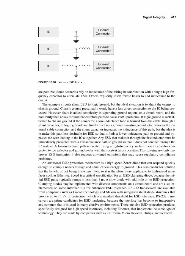
Signal Integrity 417
are possible. Some scenarios rely on inductance of the wiring in combination with a single high-fre-quency capacitor to attenuate ESD. Others explicitly insert ferrite beads to add inductance to thecircuit.
The example circuits shunt ESD to logic ground, but the ideal situation is to shunt the energy tochassis ground. Chassis ground presumably would have a less direct connection to the IC being pro-tected. However, there is added complexity in separating ground regions on a circuit board, and thepossibility then arises for unintended return paths to cause EMC problems. If logic ground is well at-tached to chassis ground at the connector, a low-inductance loop is formed from the cable, through ashunt capacitor, to logic ground, and finally to chassis ground. Inserting an inductor between the ex-ternal cable connection and the shunt capacitor increases the inductance of this path, but the idea isto make this path less desirable for ESD so that it finds a lower-inductance path to ground and by-passes the wire leading to the IC altogether. Any ESD that makes it through the first inductor must beimmediately presented with a low-inductance path to ground so that it does not conduct through theIC instead. A low-inductance path is created using a high-frequency surface mount capacitor con-nected to the inductor and ground nodes with the shortest traces possible. This filtering not only im-proves ESD immunity, it also reduces unwanted emissions that may cause regulatory complianceproblems.
An additional ESD protection mechanism is a high-speed Zener diode that can respond quicklyenough to clamp a node’s voltage and shunt excess energy to ground. This semiconductor solutionhas the benefit of not being a lowpass filter, so it is therefore more applicable to high-speed inter-faces such as Ethernet. Speed is a critical specification for an ESD clamping diode, because the ini-tial ESD pulse typically ramps in less than 1 ns. A slow diode will add little or no ESD protection.Clamping diodes may be implemented with discrete components on a circuit board and are also im-plemented on some interface ICs for enhanced ESD tolerance. RS-232 transceivers are availablefrom companies such as Linear Technology and Maxim with integrated shunt diode structures thatprovide up to 15 kV of protection, which is a standard threshold for ESD tolerance. RS-232 trans-ceivers are prime candidates for ESD hardening, because the interface has become so inexpensiveand common that it is used in many abusive environments. There are also ESD protection productsspecifically designed for high-speed interfaces, including Ethernet, that implement the same type oftechnology. They are made by companies such as California Micro Devices, Philips, and Semtech.
ICExternal
Connection
ICExternal
Connection
ICExternal
Connection
FIGURE 18.18 Various ESD filters.
-Balch.book Page 417 Thursday, May 15, 2003 3:46 PM

This page intentionally left blank.
419
CHAPTER 19
Designing for Success
A host of details allow the major components of a system to function properly. Miscellaneous topicsare often left out of many engineering discussions, because it is assumed that they will be coveredelsewhere. This chapter attempts to gather into one place some of the remaining practical issues thatmake the difference between a smooth development process and one that is punctuated by a series ofobstacles that waste time and detract from the operation of unique design elements that represent asystem’s true value.
Acquiring the necessary components and fabricating circuit boards is a mandatory step betweendesign and testing. It is important to select technologies that are appropriate for both the applicationand your own resources. Practical considerations such as business relationships and support costsmay constrain the choices of components and materials at your disposal. In extreme cases, it maynot be possible to realize certain design goals with limited resources. In other situations, alternativeimplementation strategies may have to be employed to circumvent difficulties in obtaining the mostideal component for a given application. These topics are covered first, because they should be takeninto consideration during initial conceptual and architectural definition phases of a project.
Next is a fairly simple topic near and dear to all digital systems: reset. Properly generating a resetsequence that allows a microprocessor to boot when power is applied is a task that is easy to accom-plish once learned and is usually taken for granted once it becomes reliable. However, reset is a topicthat requires introduction, because unpredictable reset behavior can become the Achilles’ heel of anotherwise fine system.
The middle of this chapter discusses debugging strategies and how troubleshooting efforts can bereduced when proper design decisions are made ahead of time. Designing a system that can be moreeasily analyzed for problems does not initially occur to some engineers as a requirement. Some engi-neers learn this lesson the hard way after a system has already been assembled, a subtle problemarises, and there is no clear way to make a diagnosis. While head scratching and frustration overmysterious problems cannot be eliminated from the development process, proper consideration fordebugging in the design phases of a project can greatly ease fault isolation.
The remainder of the chapter is devoted to support tools, both software and hardware, that assistwith the development and analysis of circuits. Schematic capture software packages are almost uni-versally known. An analog circuit simulation tool that many digital electronics engineers could em-ploy to greater advantage is Spice. Spice is presented herein, along with real circuit examples toshow how easily it can be used to answer questions that would otherwise be answered through trialand error in the lab. Once in the lab, test instruments become important partners in gaining visibilityinto the circuits’ operation. A brief introductory discussion of common test equipment provides anorientation to what may be at your disposal once a prototype is ready for testing.
-Balch.book Page 419 Thursday, May 15, 2003 3:46 PM
Copyright 2003 by The McGraw-Hill Companies, Inc. Click Here for Terms of Use.

420 Digital System Design in Practice
19.1 PRACTICAL TECHNOLOGIES
The combined semiconductor, electronics, and packaging industries develop many exciting and ad-vanced technologies each year. An engineer may be tempted to use the latest and greatest compo-nents and assembly techniques on a new project, but careful consideration should go into makingsuch decisions. Relevant constraints for any engineering organization are materials availability andcost, ease of manufacture, development resources, and general risk assessment. These constraintsdiffer among organizations. A large company with extensive experience and support resources has adifferent view of the world from that of a one-man design shop building microcontrollers. This doesnot mean that a small organization cannot successfully utilize new technology. It does mean that allorganizations must evaluate the practicality of various technologies using constraints that are appro-priate for their size and resources.
Materials availability is often a problem, even for large companies, when dealing with cutting-edge technologies or newly introduced products. Cutting-edge technology is, by definition, one thatpushes the limits of what is achievable at any given time. Pushing the limits in any discipline gener-ally carries with it the understanding that problems may arise in the early stages of product release.New technologies may also carry higher initial costs while volumes and manufacturing yields arestill low. Part of engineering is balancing the risks and benefits of new technologies. When you moveinto uncharted waters, an occasional setback is almost inevitable. Therefore, the new technology thatone may read about in the trade press or see advertised in company literature is not necessarily readyfor immediate use.
Aside from the general risk of new products, the economic strength that you represent as a cus-tomer has a significant impact on your ability to gain access to these products. If you are a semicon-ductor company that has just developed a new chip, and you have the staff to support only threeinitial customers, would you want three large customers or three small customers? Developing rela-tionships with manufacturers and their representatives can assist you in determining when a newtechnology is practical to use and when it should be allowed to mature further. This applies equallyto more mature products. Even components that have been shipping for some time may be subject toavailability problems. The term
allocation
is well known to component buyers. In a tight market,vendors will preallocate their manufacturing capacity across a set of key customers to preserve suc-cessful business relationships. Even when a product is mature and being manufactured in high vol-ume, a small customer may be unable to purchase it, because it is “on allocation.” Allocationproblems affect large companies as well in times of increased demand. The semiconductor industrytends to be quite cyclical, moving through phases of supply shortages and softness in demand.
Evaluating the risk of availability is an important step in the component selection process. Moremature components are generally easier to obtain. The exceptions to this rule are ICs that have shortproduction lives, such as some microprocessors and memory chips—especially DRAM. The micro-processor and memory markets are highly competitive, and products are sometimes phased out afterjust a few years. DRAM products are notorious for supply and obsolescence problems after theirvolumes peak within the first few years of introduction. There are certain bread-and-butter micropro-cessor and memory ICs that are supported for longer terms. These tend to be products for embeddedmarkets in which semiconductor process technology changes at a slower pace than in the main-stream computer market.
Newer products are often available only through authorized distribution companies. Many matureproducts can be purchased from catalog distributors. Catalog distributors include Digikey, JamecoElectronics, JDR Microdevices, and Mouser Electronics. Larger engineering organizations with ded-icated purchasing staff often prefer to deal with authorized distributors because of more direct accessto manufacturers. A small organization may be able to satisfy all or most of its procurement needswith catalog distributors if mature technologies are acceptable.
-Balch.book Page 420 Thursday, May 15, 2003 3:46 PM
Designing for Success 421
Manufacturability should be taken into account when selecting components, because it may beimpossible to assemble a system without expensive equipment. High-end ICs and electronic compo-nents utilize fine-pitch surface-mount technology almost exclusively because of the reduction in par-asitics and the increase in signal density. Ball grid array (BGA) packages and 0402/0201 passivecomponents are challenging to properly mount on circuit boards. They require accurate applicationof solder paste, precise positioning of components, and tightly controlled thermal profiles in solderreflow ovens. Most leaded surface mount components can actually be assembled by hand with agood quality soldering iron, although it may take some time and practice to do this. Ultra fine-pitchcomponents are extremely difficult to assemble by hand in a reliable and repeatable manner, andBGAs are impossible to mount reliably without specialized equipment. These requirements shouldbe taken into consideration according to the manufacturing facilities at your disposal. Organizationswilling to spend the money necessary for high-end systems development routinely use BGAs andother advanced packages. Products that must be assembled either by hand (e.g., small prototyperuns) or at lower-cost assembly shops that use older equipment must be designed with componentsthat are compatible with these approaches.
More complex digital ICs may require significant development resources whose costs cannot beoverlooked. When most digital systems were built from 7400 logic, the development tools requiredranged from pencil and paper to a basic schematic capture program. The barrier to entry from a toolspurchasing perspective was low and remains low for this class of design. Once a microprocessor isadded, things get a little more involved. First, a microprocessor requires boot ROM that somehowmust be programmed. EPROM—and now flash—programmers are common development tools in adigital systems lab. (Don’t forget to socket the boot ROM rather than soldering it to the PCB, so thatit can be removed for programming!) With microprocessors also come software development toolsincluding assemblers and compilers. An assembler is the minimum software tool required to workpractically with a microprocessor. Because of their relative simplicity, assemblers can be obtainedfor little or no cost for most microprocessors. Some manufacturers of embedded microprocessorsgive away assemblers to promote the use of their products. High-level language compilers (e.g., C/C++) for many microprocessors are also available at little or no cost, thanks to the GNU free soft-ware project.
Programmable logic devices require a whole other set of development tools that can get rather ex-pensive, depending on the complexity of the design and which devices are being used. An HDL suchas Verilog or VHDL is most commonly used to implement programmable logic, although some engi-neers still use schematic capture for smaller designs—a practice that was more common in the daysof less-complex digital logic. Some PLD manufacturers also support proprietary design entry meth-ods, although this support is more for legacy customers than for new mainstream business. The firststep in HDL-based design after writing the logic is to simulate it to verify its operation prior to de-bugging in the lab. It is much easier to detect a problem in simulation, because all internal logicnodes can be probed, and the circuit can be run at an arbitrarily low speed to observe its operation.Lab debugging requires equipment such as oscilloscopes and logic analyzers to view logic nodes,and less visibility is generally available as compared to a simulation. The next step is synthesis,wherein the language constructs are converted into logic gate representations. Simulation and syn-thesis tools can cost thousands or tens of thousands of dollars, although some manufacturers offervery low-cost HDL design software for smaller designs. After synthesis, the logic must be mappedand fitted to the specific chip’s internal resources. Mapping software is proprietary, based on the typeof PLD being used, because each manufacturer’s PLD has a different internal structure. This soft-ware is provided at low or no cost to customers.
Configuring PLDs once required expensive programming equipment, but most modern CPLDsand FPGAs are now in-circuit programmable via a serial or parallel interface. In fact, most CPLDsand FPGAs use EEPROM or SRAM technology, which makes them almost infinitely reprogramma-
-Balch.book Page 421 Thursday, May 15, 2003 3:46 PM

422 Digital System Design in Practice
ble so that logic mistakes do not require replacing a potentially expensive IC. Smaller, more maturePLDs may still require dedicated programming hardware, which may be reason enough to avoidthem if possible in favor of a small CPLD. The price difference between a PLD and a small CPLD isnow slim to none.
For reasons previously discussed, signal integrity software packages may be necessary when de-signing high-speed digital circuits. These tools can be quite expensive, but the consequences of notusing them can be even more costly in terms of wasted materials and time if a circuit malfunctionsbecause of signal integrity problems. Before embarking on an ambitious high-speed design, makesure that signal integrity issues are either well understood or that the resources are available forproper analysis before fabricating a prototype. Certainly, not all designs require extensive signal in-tegrity analysis. If it is known that the signal speeds and wire lengths are such that transmission lineeffects, crosstalk, and EMI can be addressed through conservative design practices, minimal analy-sis may be required. This determination generally requires someone with prior experience to reviewa design and make predictions based on previous work.
Risk assessment in choosing which components and technologies to employ is an important partof systems design. An otherwise elegant architecture can fall on its face if a key component or neces-sary development tools are unavailable. Therefore, be sure to make choices that are practical for boththe application and the resources at your disposal.
19.2 PRINTED CIRCUIT BOARDS
The selection of appropriate technologies is a convenient segue into circuit construction, because themanner in which a circuit is assembled can have a great impact on the viability of the resulting pro-totype or product. Higher-speed circuits are more sensitive to construction techniques because ofgrounding and inductance issues. Most high-speed circuits can be fabricated only with multilayerPCBs, but more options are available for slower systems, especially in the prototyping phase of aproject.
Circuit boards can be of either the printed circuit or manual point-to-point wiring variety. As al-ready discussed, PCBs consist of stacked layers of copper foil that have been uniquely etched toconnect arbitrary points in the circuit. The term “printed” refers to the standard technique of usingphotolithography to expose a chemically treated copper foil with a negative image of the desiredetching. Similar to creating a photograph, the exposure process alters the photoresistive chemicalsthat have been applied to the foil so that the exposed or nonexposed areas are etched away when thefoil is placed into a chemical acid bath. PCBs are an ideal technology, because they can be mass pro-duced with fine control over the accuracy of each unit. Simple single- and double-sided PCBs can bemanually fabricated using a variety of techniques, and the cost of having such boards professionallymanufactured is low. Multilayer PCBs must be fabricated professionally because of the complexityof creating plated vias and accurately aligning multiple layers that are etched separately and thenglued together. The major cost involved in designing a small PCB is often the specialized computeraided design (CAD) software necessary to create the many features that a PCB implements, includ-ing accurate traces, pads, and IC footprints. Low-end PCB CAD packages are available for severalhundred dollars. High-end tools run into the tens of thousands of dollars.
Once a PCB is fabricated, it is assembled along with the various components to which it is de-signed to connect. Assembly may be performed manually or at a specialized assembly firm, almostall of which use automated assembly equipment. It is difficult to manually assemble all but relativelysimple boards because of the fine-pitch components and the element of human error. Automated as-sembly equipment substantially increases reliability and improves assembly time for multipleboards, but at the expense of increase setup time to program the machines for a specific design.
-Balch.book Page 422 Thursday, May 15, 2003 3:46 PM

Designing for Success 423
Automated assembly is performed using one or two soldering techniques, depending on the typesof components on a PCB. Before the widespread use of surface mount technology (SMT), the stan-dard process was to program a pick-and-place machine to automatically insert leaded componentsinto the correct holes in the PCB. The machine trims the leads as they are inserted so that a smalllength protrudes from the bottom, or solder side, of the PCB. When the PCB is fully stuffed, it isplaced onto rails that carry it through a wave-soldering machine. A wave-soldering machine containsa bath of liquid solder over which the PCB is dragged. The metal component leads, in combinationwith the plated holes and pads of the PCB, wick molten solder up into the gaps, and the solder hard-ens as the PCB exits the molten solder wave. Wave soldering is a mature assembly technology thathas worked well for decades.
Certain design rules are necessary for successfully wave soldering a PCB and preventing excessivesolder from shorting adjacent leads. First, a PCB’s top and bottom surfaces are finished with a thinlayer of solder mask so that only metal intended for soldering is exposed. The molten solder will notadhere to the solder mask. Second, minimum lead spacing rules are followed that ensure that the leadgaps are too large for the solder to wick into them. Finally, rows of component leads are oriented in asingle line perpendicular to the solder wave to minimize solder bridges, or shorts. If the leads of aDIP package are moved through the wave abreast, or in a parallel orientation, they are more prone topicking up an excessive quantity of solder in the many gaps formed between the leads. When the DIPis rotated 90° so that the lead rows are perpendicular to the wave, the solder can more freely traveldown the narrow column and not get excessively stuck in one inter-lead gap. There are a variety ofPCB layout tricks to reduce solder bridging in wave-soldered PCBs. If your PCB is expected to beprofessionally wave soldered, it is advisable to consult the assembly firm before designing the PCB.Manufacturing engineers at assembly firms are very knowledgeable about what works and whatdoesn’t, because they work with this equipment on a daily basis. Each assembly firm has its own setof manufacturability guidelines that have been developed based on the tools at their disposal. Rulesfor one firm may not be fully in agreement with those of another. A half-hour conversation ahead oftime can save days of headaches caused by myriad short circuits in an improperly designed PCB.
Wave soldering does not work for many SMT boards, because the small gaps in fine-pitch compo-nent leads act as efficient solder sponges, resulting in completely shorted boards. SMT PCBs use asolder paste reflow assembly process. The process begins by applying solder paste to the SMT padsthrough a special stencil. The stencil has openings in the exact locations where solder paste is de-sired. A pick-and-place machine then stuffs the PCB. Careful handling of the stuffed board is neces-sary, because adhesion of the solder paste is all that holds the parts in place. Many PCBs havecomponents on both sides. In these situations, the bottom-side components are held in place with thesolder paste’s natural adhesion, which prevents them from falling off when they are upside downduring the remainder of the assembly process. Once all SMT components have been loaded onto thePCB, the PCB is moved through a reflow oven with carefully controlled temperature zones to suitthe solder, component, and PCB properties.
A PCB with both through-hole and SMT components usually requires a two-step process consist-ing of reflow followed by selective wave soldering. Selective wave soldering is accomplished withvarying types of masks that are temporarily applied over the bottom-side SMT components so thatthey do not get shorted or stripped off the board in the solder wave. It is preferable to design a PCBwithout the need for a two-step process to save both time and money in assembly. An SMT PCBwith only a few necessary through-hole components (e.g., connectors) may be more efficiently as-sembled by having a person manually solder the through-hole components after reflow.
As with wave soldering, the reflow process has its own set of manufacturing guidelines to in-crease the reliability of the manufacturing process. The intended assembly firm should be contactedbefore PCB design to fully understand its engineers’ manufacturing rules. A standard rule for bothwave soldering and reflow is to leave a minimum spacing, or
keep-out
, between the PCB edge and
-Balch.book Page 423 Thursday, May 15, 2003 3:46 PM

424 Digital System Design in Practice
all components. These keep-outs make the PCB easier to handle and allow it to ride on rails throughthe pick-and-place, wave, and reflow machines. A typical component-to-edge keep-out is 0.2 in (5mm). Very dense PCBs that cannot tolerate such keep-outs may require snap-off rails fabricated aspart of the PCB. Such rails are not uncommon and are almost free, because they are formed by rout-ing slots at the edges of a PCB as shown in Fig. 19.1. A related assembly rule is the inclusion of tool-ing holes at several locations around the PCB perimeter. These holes provide alignment andattachment points for the assembly machines.
Pick-and-place machines generally require assistance in perfectly aligning a high-pin-count SMTpackage to its designated location on the PCB. Most passive components and small multilead SMTpackages can be automatically aligned once the PCB is locked into the machine. The alignment ofpackages such as QFPs and BGAs is aided with fiducial markers that are designed into the PCB inthe vicinity of these IC locations. Fiducials are typically small circles or bull’s eye symbols etched inthe surface copper layer that can be optically detected by the pick-and-place machine as the dis-penser head closes in on the desired location. Figure 19.2 illustrates fiducial placement around QFP
Snap-Off Rail
Snap-Off Rail
Finished PCB Area
Finished PCB Area
FIGURE 19.1 Removable PCB rails.
U4
U5
Copper Pads
FiducialsSilk Screen Markers
FIGURE 19.2 Fiducial markers for SMT alignment.
-Balch.book Page 424 Thursday, May 15, 2003 3:46 PM

Designing for Success 425
footprints. Also shown are visual inked silk-screen markers for people’s benefit that are created toidentify different components with unique reference designators and to draw shapes that assist in cir-cuit assembly and troubleshooting. The fiducials do not have to be in a standard location. What isimportant is that their exact location is known and entered into the machine so that an absolute loca-tion can be determined once the fiducials are optically detected.
19.3 MANUALLY WIRED CIRCUITS
PCBs are an excellent solution for high-speed and production systems, but manual wiring may besuitable for building small quantities of lower-speed circuits. Manual wiring can be performed in avariety of ways and has the benefits of low material cost and less support infrastructure, and it is thequickest way to start building a circuit. The time and money spent designing a PCB can be amortizedacross multiple units built, but each manually wired circuit consumes the same construction re-sources. It is important to understand the limitations of manual circuit wiring, because it can takedays of tedious work to build a single circuit board. For an engineer on a budget, it may be thecheapest and quickest way to prototype a lower-speed digital system.
Breadboard
is an industry term for a blank circuit board that consists solely of equally spacedholes. A breadboard is generally made of fiberglass and has hundreds or thousands of holes alignedon 0.1-in (2.54-mm) centers to match the common pin spacing of DIPs and many other electroniccomponents. The term breadboard comes from a loose similarity to a slice of bread that is permeatedwith holes. If the breadboard is designed for solder assembly, it is built with thin copper pads aroundeach hole so that solder will adhere to the board. Some breadboards contain plated holes with padson both sides of the board for increased solder adhesion. As shown in Fig. 19.3, some breadboardsadd thin mesh planes by taking advantage of the small spaces between copper pads. These planes arenot as effective as a PCB’s continuous plane, but they have less inductance than discrete wires. Thepresence of a mesh plane is not bad, but it should not lead to the false impression that high-qualitytransmission lines can be constructed.
Building a circuit from scratch on a breadboard is done by inserting components into the boardand then running small wires, usually 30 gauge, point to point between their leads. DIPs and othercomponents with preformed leads on 0.1-in centers can be directly inserted into the board. Someconnectors, as well as TO-220 voltage regulators, transistors, and diodes, have a compatible 0.1-inlead pitch. Resistors, capacitors, and inductors with axial or radial lead configurations may requirebending their leads so that they can lie flat on the board. An axial leaded component is most com-monly in a cylindrical package with one lead protruding from the center of each face—the two leads
FIGURE 19.3 Breadboard with plated holes and mesh plane.
-Balch.book Page 425 Thursday, May 15, 2003 3:46 PM
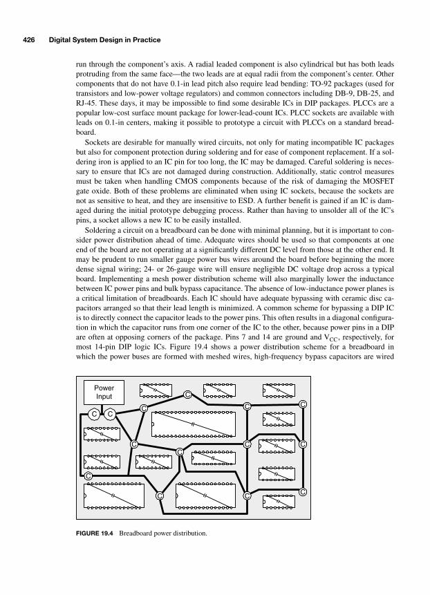
426 Digital System Design in Practice
run through the component’s axis. A radial leaded component is also cylindrical but has both leadsprotruding from the same face—the two leads are at equal radii from the component’s center. Othercomponents that do not have 0.1-in lead pitch also require lead bending: TO-92 packages (used fortransistors and low-power voltage regulators) and common connectors including DB-9, DB-25, andRJ-45. These days, it may be impossible to find some desirable ICs in DIP packages. PLCCs are apopular low-cost surface mount package for lower-lead-count ICs. PLCC sockets are available withleads on 0.1-in centers, making it possible to prototype a circuit with PLCCs on a standard bread-board.
Sockets are desirable for manually wired circuits, not only for mating incompatible IC packagesbut also for component protection during soldering and for ease of component replacement. If a sol-dering iron is applied to an IC pin for too long, the IC may be damaged. Careful soldering is neces-sary to ensure that ICs are not damaged during construction. Additionally, static control measuresmust be taken when handling CMOS components because of the risk of damaging the MOSFETgate oxide. Both of these problems are eliminated when using IC sockets, because the sockets arenot as sensitive to heat, and they are insensitive to ESD. A further benefit is gained if an IC is dam-aged during the initial prototype debugging process. Rather than having to unsolder all of the IC’spins, a socket allows a new IC to be easily installed.
Soldering a circuit on a breadboard can be done with minimal planning, but it is important to con-sider power distribution ahead of time. Adequate wires should be used so that components at oneend of the board are not operating at a significantly different DC level from those at the other end. Itmay be prudent to run smaller gauge power bus wires around the board before beginning the moredense signal wiring; 24- or 26-gauge wire will ensure negligible DC voltage drop across a typicalboard. Implementing a mesh power distribution scheme will also marginally lower the inductancebetween IC power pins and bulk bypass capacitance. The absence of low-inductance power planes isa critical limitation of breadboards. Each IC should have adequate bypassing with ceramic disc ca-pacitors arranged so that their lead length is minimized. A common scheme for bypassing a DIP ICis to directly connect the capacitor leads to the power pins. This often results in a diagonal configura-tion in which the capacitor runs from one corner of the IC to the other, because power pins in a DIPare often at opposing corners of the package. Pins 7 and 14 are ground and V
CC
, respectively, formost 14-pin DIP logic ICs. Figure 19.4 shows a power distribution scheme for a breadboard inwhich the power buses are formed with meshed wires, high-frequency bypass capacitors are wired
PowerInput
C C
C
C
C
C
C
CC
C
C C
C
C
FIGURE 19.4 Breadboard power distribution.
-Balch.book Page 426 Thursday, May 15, 2003 3:46 PM

Designing for Success 427
directly to power pins, and low-frequency bulk electrolytic capacitors are arranged throughout theboard. This hypothetical circuit contains 7400-type logic ICs in 14-, 16-, and 20-pin DIPs as well asVLSI memory and microprocessor ICs in 28- and 40-pin DIPs.
An alternative to conventional breadboards for temporary prototypes of small circuits is the
sold-erless breadboard
. A solderless breadboard isn’t a fiberglass board, but a plastic frame in whichmany small spring-clips are embedded. Holes are on 0.1-in centers, and the spring clips are typicallyarranged in rows of five contacts separated by a gap, or channel, across which a standard 0.3-in(76.2 mm) wide DIP is inserted. Figure 19.5 shows a small solderless breadboard. Power distribu-tion is often assisted by means of a continuous spring-clip bus running across the top and bottom ofthe breadboard. Connections are made by inserting solid wires between various spring clips. Sinceeach spring clip has five contacts, a maximum of five connections can be made to a single node. Ifmore are necessary, an unoccupied spring clip nearby must be used for the excess connections andthen bridged to the other spring clip via a wire. Solderless breadboards are perfect for small experi-ments and are used in many academic lab settings, because solder irons and other assembly tools arenot necessary. Clearly, solderless breadboards are not for every circuit. Aside from electrical integ-rity issues, they cannot accept common PLCC packages without a special breakout product that es-sentially converts a PLCC to a DIP. Nevertheless, substantial digital circuits can be prototyped on asolderless breadboard, including low-speed microprocessors with memory and basic peripherals.
Soldering is not the only way to prototype a digital system with permanent connections.
Wire-wrapping
is a technique that has been around for decades and was actually used for production as-sembly in many minicomputers and mainframes during the 1960s and 1970s. The wire-wrappingprocess establishes electrical connections by tightly wrapping small wire, typically 30 gauge, aroundsquare pins. Several turns of wire are made as shown in Fig. 19.6, resulting in a surprisingly durableelectromechanical connection, even without the benefit of insulation that is often stripped off. Wire-wrapping requires the use of special IC sockets with long, square posts that protrude through the bot-
Channel forDIP Mounting
Power Bus
FIGURE 19.5 Solderless breadboard.
DIP Sockets — Edge View
FIGURE 19.6 Wire-wrap connections.
-Balch.book Page 427 Thursday, May 15, 2003 3:46 PM
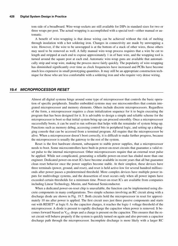
428 Digital System Design in Practice
tom side of a breadboard. Wire-wrap sockets are still available for DIPs in standard sizes for two orthree wraps per post. The actual wrapping is accomplished with a special tool—either manual or au-tomatic.
A benefit of wire-wrapping is that dense wiring can be achieved without the risk of meltingthrough insulation with a hot soldering iron. Changes in connectivity are made by unwrapping awire. However, if the wire to be unwrapped is at the bottom of a stack of other wires, those othersmay need to be removed as well. A fully manual wire-wrap process requires that a wire be cut tolength and stripped at each end to expose approximately 1 in of bare wire, and the wrapping tool isturned around the square post at each end. Automatic wire-wrap guns are available that automati-cally strip and wrap wire, making the process move fairly quickly. The popularity of wire-wrappinghas diminished significantly over time as clock frequencies have increased and PCBs have becomemuch less expensive in small prototyping quantities. It may still be an appropriate construction tech-nique for those who are less comfortable with a soldering iron and who require very dense wiring.
19.4 MICROPROCESSOR RESET
Almost all digital systems hinge around some type of microprocessor that controls the basic opera-tion of specific peripherals. Smaller embedded systems may use microcontrollers that contain inte-grated microprocessor and memory elements. Others include discrete microprocessors. Regardlessof the form, a microprocessor requires a clean initialization sequence for it to begin executing theprogram that has been designed for it. It is advisable to design a simple and reliable scheme for themicroprocessor to boot so that initial system bring-up can proceed smoothly. Once a microprocessorsuccessfully boots, it can be used to run software that helps with the remainder of system bring-up.Functions such as memory debug, accessing control bits in peripheral logic, and setting up a debug-ging console that can be accessed from a terminal program. All require that the microprocessor bealive. When a microprocessor doesn’t boot correctly, it is difficult to make further progress, becausethe microprocessor is usually the gateway to the rest of the system.
Reset is the first hardware element, subsequent to stable power supplies, that a microprocessorneeds to boot. Some microcontrollers have built-in power-on-reset circuits that guarantee a valid re-set pulse to the internal microprocessor. Other microprocessors require that an external reset pulsebe applied. While not complicated, generating a reliable power-on-reset has eluded more than oneengineer. Dedicated power-on-reset ICs have become available in recent years that all but guaranteeclean reset behavior once the power supplies become stable. At their simplest, these devices havethree terminals (power, ground, and reset), and reset is held active-low for several hundred millisec-onds after power passes a predetermined threshold. More complex devices have multiple power in-puts for multivoltage systems, and the deassertion of reset occurs only when all power inputs haveexceeded certain thresholds for a minimum time. Power-on-reset ICs are available from companiesincluding Linear Technology, Maxim, and National Semiconductor.
When a dedicated power-on-reset chip is unavailable, the function can be implemented using dis-crete components in many configurations. Two simple schemes involving an RC circuit along with adischarge diode are shown in Fig. 19.7. Both circuits hold the microprocessor in reset for approxi-mately 10 ms after power is applied. The first circuit uses just three passive components and startsout with RESET* at logic 0. As the capacitor charges, it reaches the logic-1 voltage threshold of themicroprocessor. A diode is present to rapidly discharge the capacitor when power is removed. It be-comes forward biased as V
CC
drops and a charge is present on the capacitor. This ensures that the re-set circuit will behave properly if the system is quickly turned on again and also prevents a capacitordischarge path through the microprocessor. Incomplete discharge is more likely with a larger RC
-Balch.book Page 428 Thursday, May 15, 2003 3:46 PM
Designing for Success 429
time constant, as is required by some microprocessors. Better results are obtained using a Schottkydiode, because its lower forward voltage discharges the capacitor to a lower voltage.
The second circuit is more robust, because it uses a Schmitt trigger to drive the microprocessor’sinput, guaranteeing a clean digital transition despite variations in the slope of the RC voltage curve.This is especially helpful when long RC time constants are required to generate long reset pulses asdictated by a microprocessor. A 74LS14 or similar Schmitt-trigger logic gate may be convenient todesign into a system, and it can be used in places other than the power-on-reset circuit. Alternatively,a smaller voltage comparator can be used to implement the same function by designing in hysteresis.Before power-on, the inverter input node is at 0 V. At power-on, the voltage step of the power supplypasses through the capacitor, because the voltage across the capacitor is initially 0 V and brings theinput node to a logic-1 voltage, which in turn causes RESET* to be driven to logic 0. The resistor im-mediately begins pulling the voltage toward ground and eventually causes RESET* to be deasserted.The diode is present to clamp the inverter input node to ground during power-down. Clamping is de-sirable, because the resistor has already pulled the input node to ground and, without the diode, anegative V
CC
step would force the input node to a negative voltage. When the diode is present, the in-put node remains near 0 V and is able to serve its intended purpose during an immediate power-on.The diode also prevents a large negative voltage from potentially damaging the inverter.
Power-on is not the only condition in which a microprocessor reset may be desired. Especiallyduring the debugging process, it can be very useful to have a reset button that can quickly restart thesystem from a known initial state when software under development encounters fatal bugs. Many ofthe aforementioned power-on-reset ICs contain circuitry to
debounce
an external pushbutton. When abutton is pushed, it may appear that a clean electrical connection is made and then broken when thebutton is released. In reality, the contact and release events of a button are noisy for brief periods oftime as the internal metal contacts come into contact with each other. This noise or bounce may lastonly a few milliseconds, but it can cause a microprocessor to improperly exit its reset state. Debounc-ing is the process of converting the noisy edges of a pushbutton into a clean pulse. Filtering is a gen-eral solution for debouncing a noisy event and can be performed in an analog fashion or digitally bytaking multiple samples of the event and forcing the bouncing samples to one state or the other.
19.5 DESIGN FOR DEBUG
“To err is human” is a truism that directly applies to engineering. The engineering process is a com-bination of design and debugging in which inevitable problems in the original implementation are
VCC
1 µF
10 k Ω
RESET*
VCC
1 µF
RESET*
10 k Ω
FIGURE 19.7 Discrete power-on-reset circuits.
-Balch.book Page 429 Thursday, May 15, 2003 3:46 PM
430 Digital System Design in Practice
detected and fixed. Hardware problems include logic mistakes, incorrect circuit board connections,and improperly assembled systems. Regardless of its nature, a problem must be isolated before itcan be corrected. Bugs can be hard to find in a digital system, because time is measured in nanosec-onds, and logic 1s and 0s are not visually distinct as they flow across wires. The debugging processis made easier by employing specific design elements and methodologies that improve visibility intoa system’s inner workings.
A basic debugging aid is the ability to probe a digital circuit with an oscilloscope or logic ana-lyzer so that the state of individual wires can be observed. (A logic analyzer is a tool that rapidlycaptures a set of digital signals and then displays them for inspection. Test equipment is discussed inmore detail later on.) Some circuits require little or no modification to gain this visibility, dependingon their density, packaging technology, and operating speed. A circuit that uses DIPs or PLCCs ex-clusively can be directly probed with an oscilloscope probe, and clip-on logic analyzer adapters maybe used to capture many digital signals simultaneously. As circuits get denser and use fine-pitch sur-face mount ICs, it becomes necessary to use connectors specifically designed for logic analyzer at-tachment. The correct type of connector should be verified with your logic analyzer manufacturer.Using logic analyzer connectors provides access to a set of predetermined signals fairly rapidly, be-cause a whole connector can be inserted or removed at one time rather than having to use individualclips for each signal.
Logic analyzer probing becomes more of a challenge at high frequencies because of transmissionline effects. Top-of-the-line logic analyzers are designed to minimally load a bus, and they includecontrolled impedance connectors to reduce unwanted side effects of probing. Depending on the tracelengths involved and the specific ICs, minimal impact is possible with speeds around 100 MHz.Careful PCB layout is essential for these situations, and it is desirable to minimize stubs created byrouting signals to the connectors. At frequencies above 100 MHz, transmission line effects can rap-idly cause problems, and special impedance matching and terminating circuitry may be necessary toachieve nonintrusive logic analyzer probing. Logic analyzer manufacturers have circuit recommen-dations that are specifically customized to their products.
The ideal scenario is to have logic analyzer visibility for every signal in a system. In reality, 100percent visibility is not practical. More complex buses are more difficult to debug and, consequently,stand to benefit more from logic analyzer connectors. A simple asynchronous microprocessor bus,on the other hand, can be debugged with an inexpensive analog oscilloscope if a logic analyzer is notavailable. Whereas logic analyzers stop time and display a timing diagram of the selected signalsover a short span of time, analog oscilloscopes usually do not have this persistence. The persistenceproblem can be addressed with a technique known as a
scope loop
. A scope loop is usually imple-mented in software but can be done in hardware as well, and it performs the same simple operationcontinuously so that an oscilloscope can be used to observe what has become a periodic event.
Debugging a basic microprocessor bus problem with a scope loop can be explained with a briefexample. Figure 19.8 shows a portion of a digital system in which a RAM is connected to a micro-processor and enabled with an address decoder. In normal operation, the microprocessor asserts anaddress that is recognized by the decoder, and the RAM is enabled. One possible bug is an incor-rectly wired address decoder. If the microprocessor is unable to access the RAM, the first thing tocheck is whether the RAM’s chip select is being asserted. A single RAM access cannot be effec-tively observed on a normal analog oscilloscope, because the event may last well under a microsec-ond. Instead, a scope loop can be created by programming the microprocessor to continuallyperform RAM reads. The chip select can now be observed on an oscilloscope, because it is a peri-odic event. If the chip select is not present, the address decoder’s inputs and output can be tested oneby one to ensure proper connectivity. If the chip select is being asserted, other signals such as outputenable or individual address bits can be probed. Oscilloscopes have at least two channels, and thesecond channel can be used to probe one other signal in conjunction with chip select to observe rela-
-Balch.book Page 430 Thursday, May 15, 2003 3:46 PM
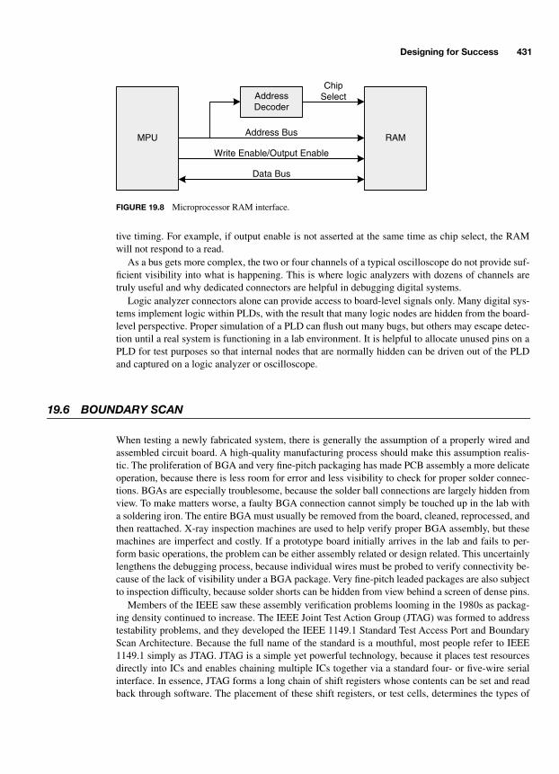
Designing for Success 431
tive timing. For example, if output enable is not asserted at the same time as chip select, the RAMwill not respond to a read.
As a bus gets more complex, the two or four channels of a typical oscilloscope do not provide suf-ficient visibility into what is happening. This is where logic analyzers with dozens of channels aretruly useful and why dedicated connectors are helpful in debugging digital systems.
Logic analyzer connectors alone can provide access to board-level signals only. Many digital sys-tems implement logic within PLDs, with the result that many logic nodes are hidden from the board-level perspective. Proper simulation of a PLD can flush out many bugs, but others may escape detec-tion until a real system is functioning in a lab environment. It is helpful to allocate unused pins on aPLD for test purposes so that internal nodes that are normally hidden can be driven out of the PLDand captured on a logic analyzer or oscilloscope.
19.6 BOUNDARY SCAN
When testing a newly fabricated system, there is generally the assumption of a properly wired andassembled circuit board. A high-quality manufacturing process should make this assumption realis-tic. The proliferation of BGA and very fine-pitch packaging has made PCB assembly a more delicateoperation, because there is less room for error and less visibility to check for proper solder connec-tions. BGAs are especially troublesome, because the solder ball connections are largely hidden fromview. To make matters worse, a faulty BGA connection cannot simply be touched up in the lab witha soldering iron. The entire BGA must usually be removed from the board, cleaned, reprocessed, andthen reattached. X-ray inspection machines are used to help verify proper BGA assembly, but thesemachines are imperfect and costly. If a prototype board initially arrives in the lab and fails to per-form basic operations, the problem can be either assembly related or design related. This uncertainlylengthens the debugging process, because individual wires must be probed to verify connectivity be-cause of the lack of visibility under a BGA package. Very fine-pitch leaded packages are also subjectto inspection difficulty, because solder shorts can be hidden from view behind a screen of dense pins.
Members of the IEEE saw these assembly verification problems looming in the 1980s as packag-ing density continued to increase. The IEEE Joint Test Action Group (JTAG) was formed to addresstestability problems, and they developed the IEEE 1149.1 Standard Test Access Port and BoundaryScan Architecture. Because the full name of the standard is a mouthful, most people refer to IEEE1149.1 simply as JTAG. JTAG is a simple yet powerful technology, because it places test resourcesdirectly into ICs and enables chaining multiple ICs together via a standard four- or five-wire serialinterface. In essence, JTAG forms a long chain of shift registers whose contents can be set and readback through software. The placement of these shift registers, or test cells, determines the types of
MPU RAM
AddressDecoder
ChipSelect
Data Bus
Write Enable/Output Enable
Address Bus
FIGURE 19.8 Microprocessor RAM interface.
-Balch.book Page 431 Thursday, May 15, 2003 3:46 PM
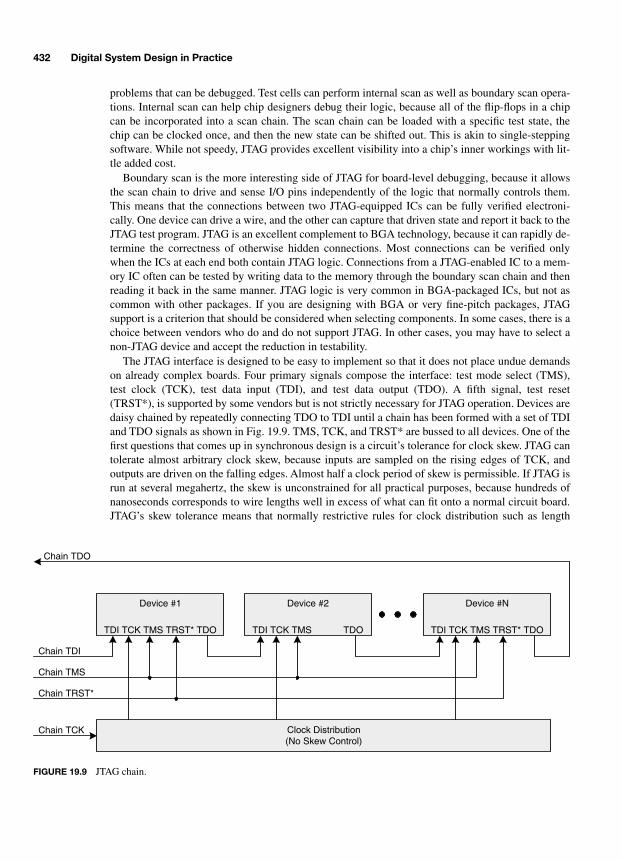
432 Digital System Design in Practice
problems that can be debugged. Test cells can perform internal scan as well as boundary scan opera-tions. Internal scan can help chip designers debug their logic, because all of the flip-flops in a chipcan be incorporated into a scan chain. The scan chain can be loaded with a specific test state, thechip can be clocked once, and then the new state can be shifted out. This is akin to single-steppingsoftware. While not speedy, JTAG provides excellent visibility into a chip’s inner workings with lit-tle added cost.
Boundary scan is the more interesting side of JTAG for board-level debugging, because it allowsthe scan chain to drive and sense I/O pins independently of the logic that normally controls them.This means that the connections between two JTAG-equipped ICs can be fully verified electroni-cally. One device can drive a wire, and the other can capture that driven state and report it back to theJTAG test program. JTAG is an excellent complement to BGA technology, because it can rapidly de-termine the correctness of otherwise hidden connections. Most connections can be verified onlywhen the ICs at each end both contain JTAG logic. Connections from a JTAG-enabled IC to a mem-ory IC often can be tested by writing data to the memory through the boundary scan chain and thenreading it back in the same manner. JTAG logic is very common in BGA-packaged ICs, but not ascommon with other packages. If you are designing with BGA or very fine-pitch packages, JTAGsupport is a criterion that should be considered when selecting components. In some cases, there is achoice between vendors who do and do not support JTAG. In other cases, you may have to select anon-JTAG device and accept the reduction in testability.
The JTAG interface is designed to be easy to implement so that it does not place undue demandson already complex boards. Four primary signals compose the interface: test mode select (TMS),test clock (TCK), test data input (TDI), and test data output (TDO). A fifth signal, test reset(TRST*), is supported by some vendors but is not strictly necessary for JTAG operation. Devices aredaisy chained by repeatedly connecting TDO to TDI until a chain has been formed with a set of TDIand TDO signals as shown in Fig. 19.9. TMS, TCK, and TRST* are bussed to all devices. One of thefirst questions that comes up in synchronous design is a circuit’s tolerance for clock skew. JTAG cantolerate almost arbitrary clock skew, because inputs are sampled on the rising edges of TCK, andoutputs are driven on the falling edges. Almost half a clock period of skew is permissible. If JTAG isrun at several megahertz, the skew is unconstrained for all practical purposes, because hundreds ofnanoseconds corresponds to wire lengths well in excess of what can fit onto a normal circuit board.JTAG’s skew tolerance means that normally restrictive rules for clock distribution such as length
Device #1
TDI TCK TMS TRST* TDO
Device #2
TDI TCK TMS TDO
Device #N
TDI TCK TMS TRST* TDO
Chain TDI
Chain TMS
Chain TRST*
Chain TCK Clock Distribution(No Skew Control)
Chain TDO
FIGURE 19.9 JTAG chain.
-Balch.book Page 432 Thursday, May 15, 2003 3:46 PM

Designing for Success 433
matching and low-skew buffers can be largely ignored. Of course, signal integrity considerationsstill apply so that TCK is delivered without excessive distortion to each IC. TRST* is active low andallows supporting devices to have their JTAG logic restarted. TMS is active high and places an ICinto test mode by activating its JTAG controller.
JTAG scan chains are normally operated with special software designed to apply and check user-defined test patterns, or vectors. IC manufacturers who support JTAG provide boundary scan de-scription language (BSDL) files that tell JTAG software how to interact with an IC. A standard pro-cedure is to combine a PCB netlist (a file that lists each connection on the board in detail) withmultiple BSDL files in a JTAG software package to come up with a set of test vectors. These vectorsare then run through each board after it is assembled to verify connectivity between JTAG-equippeddevices. Vendors of JTAG testing packages include Asset InterTech, Corelis, and JTAG Technolo-gies. Verifying an assembled PCB with JTAG can save days of manual debugging when there maybe problems in the assembly of BGA and fine-pitch components.
19.7 DIAGNOSTIC SOFTWARE
Software can help the debugging process by implementing scope loops, but the potential exists formuch higher-level assistance. Special-purpose diagnostic programs are extremely helpful in detect-ing problems that could otherwise take much more time to isolate. The basic idea behind a diagnos-tic is for the software to thoroughly test elements of the hardware one at a time. A complete memorydiagnostic, for example, would test every bit in every memory location. If the test fails, the nature ofthe failure provides valuable clues as to what is wrong. If there is a pattern to the failure, an improp-erly connected address or data bit may be the culprit. If the pattern is random, there may be a timingproblem that causes marginal behavior over time or the device may be bad. Diagnostics are useful inseveral phases of development, including initial debug, extended reliability testing, troubleshootingdamaged systems, and screening newly fabricated systems in either laboratory or manufacturing en-vironments.
During initial debug, when little has already been shown to work, diagnostics can serve as bothscope loops and sources of stimulation that exercise a wide range of functionality so that all featurescan be tested at least once. Memory tests are one of the most common classes of diagnostics, be-cause a reliable memory interface is critical to any microprocessor-based system’s operation. It isimpractical to manually test millions of memory locations, but a program can easily perform thistask in a quick, automated fashion. The specific patterns that a memory diagnostic uses should bechosen with knowledge of potential problems that may be uncovered. These patterns are written tomemory in a complete write pass and then verified on a subsequent read pass. It is undesirable to testone memory location at a time, because certain problems can lie hidden from this approach. If thedata bus is not connected, simple capacitance on the data wires might allow the microprocessor to“read” back a data value that was just written.
Aside from timing problems that can affect all transactions, circuit board connections are primecandidates for trouble because of potential errors during assembly or subsequent damage from ex-cessive handling. A good diagnostic will pass only if there are no shorts or opens in the address, con-trol, and data bus wiring. A shorted or open control signal will generally be easiest to find, becausemany, if not all, memory accesses are affected by these faults. Data bus wiring problems manifestthemselves as a failure to read or write certain values to individual bit positions. An open data bitwire would result in reading a constant or random value, depending on the specific circuit. If a databit is shorted to ground or power, the read value would be stuck at that logic level. If two data bitsare shorted together, they will always assume the same value and will not be independently written.
-Balch.book Page 433 Thursday, May 15, 2003 3:46 PM

434 Digital System Design in Practice
Address bus wiring problems result in aliasing or an unexpected displacement within the memoryrange. In a 16-bit addressing range, a disconnected A[15] would float to a default logic level and re-sult in the lower and upper 32,768 locations overlapping. If A[15] and A[14] were shorted together,the two bits would have only two logic states instead of four, causing the middle 32k of the addressspace to overlap with the upper and lower 16k regions.
It may be useful to have multiple memory diagnostics to help with different phases of debugging.Some engineers like basic walking-ones and walking-zeroes patterns to quickly determine if anydata bits are stuck. As their names imply, walking-ones and walking-zeroes tests set all bits in a wordto one state and then walk the opposite state across each bit position. An eight-bit walking ones testcould look like this: 00000001, 00000010, 00000100, 00001000, 00010000, 00100000, 01000000,10000000. These tests verify that each bit position can be independently set to a 0 or 1 without inter-ference from neighboring bits.
Testing an entire memory after simple data bus wiring problems are resolved can be done effi-ciently by selecting a set of appropriate data patterns. Pattern selection depends on the diagnosticgoals. Is it sufficient to verify only stuck address bits? Both stuck address and data bits? Or is it nec-essary to verify every unique bit in a memory array? Stuck data bits can be uncovered with a quickwalking-ones and walking-zeroes test targeted to just a few memory locations. It is important to sep-arate the write and read phases of a short diagnostic, and therefore use multiple memory locations, toguarantee that the microprocessor is not merely reading back bus capacitance. Isolating and verify-ing every bit in a memory array can be a more complex operation than first imagined, because spe-cific memory design aspects at both the board and chip levels may require application specificpatterns to achieve 100 percent coverage. A common memory diagnostic approach is to first test forstuck data bits in a quick test and then verify the address bus with a longer test and, in the process,achieve good, but incomplete, bit coverage. This level of coverage in concert with the testing that isperformed by semiconductor manufacturers provides a high degree of confidence in the memorysystem’s integrity.
Verifying address bus and decode logic integrity can be done with a set of ramp patterns. Eachmemory location is ideally written with a unique value, but this is not possible in systems where thedata bus width is less than the address bus width. A microprocessor with 32-bit wide memory busand 2
20
locations can write a unique incrementing address into each word during a write phase andthe verify on a subsequent read phase. A system with an 8-bit memory and 65,536 locations cannotwrite unique values in a single pass. An initial approach to verifying a 64-kB memory array is towrite a repeating ramp pattern from 0x00 to 0xFF throughout memory and then read it back. Thistests only the lower half of the address bus, because there are only 256 unique values written. Alias-ing is a potential problem, because a 256-byte memory would appear identical to a 64-kB memorywithout further effort. The diagnostic requires a second pass to test the upper half of the address busby writing the MSB of the address to each byte. Each pass is incomplete on its own, but togetherthey are an effective diagnostic.
There are many memory diagnostic techniques, and engineers have their own favorites. The re-peating, alternating pattern of 0x55 and 0xAA is popular, because it provides some verification thateach bit position can hold a 1 or 0 independent of its nearest neighbors. This is in contrast to the pat-tern of 0x00 and 0xFF that could pass even if every data bit were shorted to every other data bit.However, 0x55 and 0xAA cannot isolate all data bus problems, because there is no restriction thatshorts must occur between directly adjacent bits. Traces on a PCB are routed in many arbitrary pat-terns and shorts between nonadjacent bits are possible.
Each system requires a customized diagnostics suite, because each system has different memoryand I/O resources that need to be tested. Serial communications diagnostics are common, becausemost systems have serial ports. A loop-back cable is connected to the serial port so that all datatransmitted is received at the same time. The loop-back forms a complete data path that can be auto-
-Balch.book Page 434 Thursday, May 15, 2003 3:46 PM

Designing for Success 435
matically tested with software. Pseudorandom patterns are sent out and checked on the receive sideto verify proper serial port operation. The same basic test can be performed on many types of com-munications interfaces, including Ethernet.
Diagnostic software not only assists during initial debugging, it can also be used for extended sta-bility and reliability testing where continual exercise of logic and data paths provides confidence in adesign’s integrity. Verifying proper memory accesses for a brief duration in a laboratory setting is in-sufficient for a production or high-reliability environment, because semiconductors are subject tovariation over individual units, temperature, and voltage. Once a system appears to be functioningproperly, it should be subjected to a
four-corners
test procedure. Four-corners testing subjects a sys-tem to the four worst-case permutations of temperature and voltage to ensure that there are no timingproblems over the system’s intended range of operation. It is called four-corners because tempera-ture and voltage effects on timing can be represented graphically on Cartesian coordinates as shownin Fig. 19.10. As the temperature drops and voltage increases, the speed of a logic gate increases.Conversely, the gate slows down as temperature rises and voltage drops. Both extremes can causeproblems if incorrect timing analysis was performed.
The first step in extended testing is often to run a diagnostic loop overnight and verify that therewere no failures after millions of iterations. This is usually performed at room temperature (25°C)and nominal voltage conditions. With nominal conditions verified, a thermal chamber is used tomaintain high and low temperatures for long durations as voltage is varied from high to low. Increas-ing confidence is gained when multiple systems are run through four-corners testing. Thermal cham-bers can be rented from a testing firm if you do not have the financial resources to acquire one. Acommon commercial operating temperature range is 0 to 50°C (32 to 122°F), and common digitalvoltage supplies are specified with a tolerance of ±5 percent. A diagnostic loop would be run for along period of time at each of the four combinations of temperature and voltage. When multiple sup-plies exist in a system, a case can be made for more permutations of test cases. This can becomequite burdensome with three or four different voltage rails. The decision must be made according tothe requirements and context of each situation.
An investment of time in diagnostic development also pays dividends when manufacturing newcircuit boards and systems by providing a ready-to-use testing regimen. Once a new system passes a
Temperature
Voltage
Slower
Faster
Low TemperatureHigh Voltage
Low TemperatureLow Voltage
High TemperatureLow Voltage
High TemperatureHigh Voltage
FIGURE 19.10 Four-corners effects on semiconductors.
-Balch.book Page 435 Thursday, May 15, 2003 3:46 PM

436 Digital System Design in Practice
comprehensive diagnostic suite, it can be packaged and shipped to a customer. Similarly, systemsmay come back from the field or from development work in the laboratory with damage from exces-sive handling, and diagnostics can be run to help isolate and fix the problems.
19.8 SCHEMATIC CAPTURE AND SPICE
Various types of computer aided design (CAD) software assist digital engineers in designing and im-plementing circuits and systems. Some types of CAD tools have already been discussed, includingHDL simulators, PLD fitters, and electromagnetic field solvers. Perhaps the most universal CADtool for electrical engineers of all disciplines is a schematic capture program. Schematic capture is tocircuits what word processing is to text. At the most basic level, schematic capture programs allowthe drawing and manipulation of graphical symbols. However, their utility extends to converting theinformation represented by the graphical connections into varying types of data formats used in sub-sequent stages of system development. Two of the most common and useful data conversion resultsare a
bill of materials
(BOM) and a
netlist
. A BOM is a complete summary of all components usedin the schematic and generally has identical components grouped together so that one can quicklydetermine how many units of each component are used in a design.
A netlist is an exhaustive list of all the electrical connections in the schematic and is the means oftransferring a schematic into a PCB layout program. With a schematic in hand, a circuit can be pro-totyped with either a manual wiring process or a tedious manual PCB design process. Both of thesemethods involve a person translating each drawn wire in the schematic into a wire on a circuit board.The assembly complexity and potential for errors increase as the design itself gets larger. The advan-tage of an automatically generated netlist is that errors are minimized as the entire design database istransferred from the schematic capture tool to the PCB layout tool. Each layout tool has its own pro-prietary data interchange format, so it is important for a schematic capture program to support thedesired data format.
A wide variety of schematic capture programs are available, and they range in price from hun-dreds to many thousands of dollars, depending on their intended application. Major vendors includeCadence, OrCAD (owned by Cadence), Innoveda, and Mentor Graphics. At least one program, Or-CAD, is available in a free student/demonstration edition that has limited features and can be used todraw circuits of moderate complexity.
Another CAD program that is applicable to many disciplines is the
Spice
family of analog simula-tors. Spice (or SPICE), an acronym for
simulation program with integrated circuit emphasis,
wasoriginally developed at the University of California at Berkeley in the 1970s and has become a stan-dard means of simulating circuit behavior. Many variants of Spice are available, and source code isavailable as well. Spice tools share a common basic syntax and feature set. Circuits have tradition-ally been represented manually in a netlist-like format for Spice processing. However, some vendorsnow enable schematic capture software to convert a drawn circuit into the Spice input format.PSpice is a well known variant that has been available for PC platforms for many years. It is nowsold by Cadence, which has continued the practice of offering free student and demonstration ver-sions. PSpice was used to evaluate some of the analog circuits and concepts discussed in this book.
Spice is a powerful tool. Two of its basic modes of operation are AC sweep and transient analysis.AC sweep performs frequency-domain analysis on a circuit and is used to characterize filters and thefrequency response of general circuits. Transient analysis provides a time-domain view of an analogcircuit and can be used to simulate a transmission line or view a filter’s output in the time domain asit would be seen on an oscilloscope. Spice simulations are an excellent means of performing “what-if” evaluations of circuits while still in the design phase. Transmission line terminations can be eval-uated to gauge signal integrity, and filters can be tested to determine the frequencies over which they
-Balch.book Page 436 Thursday, May 15, 2003 3:46 PM

Designing for Success 437
are effective. The degree to which a Spice simulation matches reality depends on how closely thereal conditions are modeled. Performing highly accurate simulations is a skill that requires a thor-ough understanding of circuit theory. However, useful first-order approximations of analog behaviorcan be readily achieved. A key source of divergence between simulation and reality in a digital de-sign is the parasitic properties of wires and components that become significant at high frequencies.An idealized resistor or wire might require the explicit addition of parasitic inductance and capaci-tance to get a more accurate simulation.
A basic example of Spice simulation can be shown using the first-order RC filter in Fig. 19.11.This lowpass filter uses idealized components and has f
C
≈
10 MHz with a steady attenuation slopeof 20 dB per decade.
Circuits are presented to Spice by uniquely naming or numbering each node and then instanti-ating circuit elements that reference those node names. Figure 19.12 shows the Spice circuit descrip-tion for the idealized RC filter. Ground is represented as 0. Resistors and capacitors are designatedwith identifiers beginning with R and C, respectively. V denotes a voltage source, and this voltagesource is specified with a 0-V DC component and a 1-V AC component. The
.AC
command in-structs Spice to perform an AC sweep over a logarithmic (decade) range from 100 kHz to 1 GHzwith 10 data points per decade. Note that the voltage source does not specify a frequency. This is be-cause our simulation is an AC sweep that evaluates a range of frequencies. Finally,
.PROBE
in-structs Spice to display the results graphically.
The expected filter transfer function in Fig. 19.13 is obtained following a brief simulation of thecircuit description input.
Improving the simulation’s realism can be achieved by introducing parasitic inductance in serieswith the ideal capacitor. The actual inductance varies with package type and the wiring scheme used.
V1 VIN 0 DC 0Vdc AC 1Vac R1 VIN VOUT 75 C1 0 VOUT 220p .AC DEC 10 1e5 1e9 .PROBE .END
FIGURE 19.12 Spice circuit description for ide-alized RC filter.
220 pF
75 ΩVOUTVIN
V1 R1
C1
FIGURE 19.11 Idealized RC filter for Spiceanalysis.
0.001
0.01
0.1
1
1.00E+05 1.00E+06 1.00E+07 1.00E+08 1.00E+09
Frequency (Hz)
No
rmal
ized
Am
plit
ud
e
FIGURE 19.13 Bode magnitude plot for idealized RC filter.
-Balch.book Page 437 Thursday, May 15, 2003 3:46 PM

438 Digital System Design in Practice
For the sake of discussion, 2 nH is selected to observe the effects of parasitic inductance. The previ-ous circuit description is modified as shown in Fig. 19.14. A new node is created,
PARA
, that is usedto place the inductor between the output node and the capacitor.
Running the simulation with the added parasitic inductor yields a transfer function that has simi-lar characteristics up to a decade past f
C
, and then a notch is observed, after which the attenuationactually decreases because of the inductor’s increasing impedance at high frequencies (Fig. 19.15).Increasing the parasitic inductance, as would be experienced with a leaded capacitor, would causethe notch to move to lower frequencies in simulation.
Transmission line analysis can be performed with Spice’s transient analysis capability. Differenttermination circuits and transmission line topologies can be investigated in varying degrees of detail,depending on the accuracy of the models used. It may be difficult to generate an accurate model ofan IC driver or receiver, but relatively good estimates can be obtained by combining multiple idealelements. The circuit shown in Fig. 19.16 uses a pulse voltage source with a 5-
Ω
series resistor tosimulate the driver’s output resistance and an inductor to represent the IC package’s lead inductance.
V1 VIN 0 DC 0Vdc AC 1Vac R1 VIN VOUT 75 L1 PARA VOUT 2nh C1 0 PARA 220p .AC DEC 10 1e5 1e9 .PROBE .END
FIGURE 19.14 Bode magnitude plot for RC fil-ter with parasitic inductance.
0.001
0.01
0.1
1
1.00E+05 1.00E+06 1.00E+07 1.00E+08 1.00E+09
Frequency (Hz)
No
rmal
ized
Am
plit
ud
e
FIGURE 19.15 Bode magnitude plot for RC filter with parasitic inductance.
5 pF
5 ΩVOUTVDRIVE
4n
V1 RS
VDIE
LPKG
VPIN47 Ω
RT
VIN ZO = 50 Ω
T1
TD = 1n
CL
10 kΩ
RL
FIGURE 19.16 Transmission line circuit.
-Balch.book Page 438 Thursday, May 15, 2003 3:46 PM
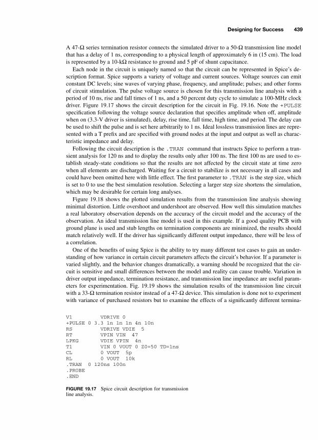
Designing for Success 439
A 47-
Ω
series termination resistor connects the simulated driver to a 50-
Ω
transmission line modelthat has a delay of 1 ns, corresponding to a physical length of approximately 6 in (15 cm). The loadis represented by a 10-k
Ω
resistance to ground and 5 pF of shunt capacitance.Each node in the circuit is uniquely named so that the circuit can be represented in Spice’s de-
scription format. Spice supports a variety of voltage and current sources. Voltage sources can emitconstant DC levels; sine waves of varying phase, frequency, and amplitude; pulses; and other formsof circuit stimulation. The pulse voltage source is chosen for this transmission line analysis with aperiod of 10 ns, rise and fall times of 1 ns, and a 50 percent duty cycle to simulate a 100-MHz clockdriver. Figure 19.17 shows the circuit description for the circuit in Fig. 19.16. Note the
+PULSE
specification following the voltage source declaration that specifies amplitude when off, amplitudewhen on (3.3-V driver is simulated), delay, rise time, fall time, high time, and period. The delay canbe used to shift the pulse and is set here arbitrarily to 1 ns. Ideal lossless transmission lines are repre-sented with a T prefix and are specified with ground nodes at the input and output as well as charac-teristic impedance and delay.
Following the circuit description is the
.TRAN
command that instructs Spice to perform a tran-sient analysis for 120 ns and to display the results only after 100 ns. The first 100 ns are used to es-tablish steady-state conditions so that the results are not affected by the circuit state at time zerowhen all elements are discharged. Waiting for a circuit to stabilize is not necessary in all cases andcould have been omitted here with little effect. The first parameter to
.TRAN
is the step size, whichis set to 0 to use the best simulation resolution. Selecting a larger step size shortens the simulation,which may be desirable for certain long analyses.
Figure 19.18 shows the plotted simulation results from the transmission line analysis showingminimal distortion. Little overshoot and undershoot are observed. How well this simulation matchesa real laboratory observation depends on the accuracy of the circuit model and the accuracy of theobservation. An ideal transmission line model is used in this example. If a good quality PCB withground plane is used and stub lengths on termination components are minimized, the results shouldmatch relatively well. If the driver has significantly different output impedance, there will be less ofa correlation.
One of the benefits of using Spice is the ability to try many different test cases to gain an under-standing of how variance in certain circuit parameters affects the circuit’s behavior. If a parameter isvaried slightly, and the behavior changes dramatically, a warning should be recognized that the cir-cuit is sensitive and small differences between the model and reality can cause trouble. Variation indriver output impedance, termination resistance, and transmission line impedance are useful param-eters for experimentation. Fig. 19.19 shows the simulation results of the transmission line circuitwith a 33-
Ω
termination resistor instead of a 47-
Ω
device. This simulation is done not to experimentwith variance of purchased resistors but to examine the effects of a significantly different termina-
V1 VDRIVE 0 +PULSE 0 3.3 1n 1n 1n 4n 10n RS VDRIVE VDIE 5 RT VPIN VIN 47 LPKG VDIE VPIN 4n T1 VIN 0 VOUT 0 Z0=50 TD=1ns CL 0 VOUT 5p RL 0 VOUT 10k .TRAN 0 120ns 100n .PROBE .END
FIGURE 19.17 Spice circuit description for transmissionline analysis.
-Balch.book Page 439 Thursday, May 15, 2003 3:46 PM
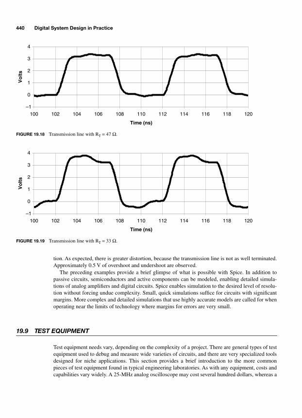
440 Digital System Design in Practice
tion. As expected, there is greater distortion, because the transmission line is not as well terminated.Approximately 0.5 V of overshoot and undershoot are observed.
The preceding examples provide a brief glimpse of what is possible with Spice. In addition topassive circuits, semiconductors and active components can be modeled, enabling detailed simula-tions of analog amplifiers and digital circuits. Spice enables simulation to the desired level of resolu-tion without forcing undue complexity. Small, quick simulations suffice for circuits with significantmargins. More complex and detailed simulations that use highly accurate models are called for whenoperating near the limits of technology where margins for errors are very small.
19.9 TEST EQUIPMENT
Test equipment needs vary, depending on the complexity of a project. There are general types of testequipment used to debug and measure wide varieties of circuits, and there are very specialized toolsdesigned for niche applications. This section provides a brief introduction to the more commonpieces of test equipment found in typical engineering laboratories. As with any equipment, costs andcapabilities vary widely. A 25-MHz analog oscilloscope may cost several hundred dollars, whereas a
–1
0
1
2
3
4
100 102 104 106 108 110 112 114 116 118 120
Time (ns)
Vo
lts
FIGURE 19.18 Transmission line with RT = 47 Ω.
–1
0
1
2
3
4
100 102 104 106 108 110 112 114 116 118 120
Time (ns)
Vo
lts
FIGURE 19.19 Transmission line with RT = 33 Ω.
-Balch.book Page 440 Thursday, May 15, 2003 3:46 PM

Designing for Success 441
1-GHz digital oscilloscope can cost tens of thousands of dollars. Both oscilloscopes perform thesame basic function, but one performs that function at much higher frequencies and with more pow-erful measurement features. The following companies are among those who manufacture some or allof the test equipment mentioned in the following text: Agilent Technologies, B&K Precision, Fluke,Kenwood, LeCroy, and Tektronix.
Perhaps the most basic test tool is the
multimeter
, available in analog and digital varieties. A digi-tal multimeter is called a
DMM
. Multimeters measure voltage, resistance, current, and sometimescapacitance, inductance, and diode forward voltages. Measuring voltage and current are passivefunctions, but the other capabilities require injecting current into a component under test to discernits voltage or other properties. DMMs are very common because of their low cost and ease of use.
Another relatively inexpensive test device is called a
logic probe
and is useful for engineers on abudget. A logic probe is placed onto a digital signal, and its indicators, visual and/or audible, tellwhether a logic 0 or logic 1 is present and whether the line is clocking or pulsing high or low. Verybasic debugging can be done with a logic probe in the absence of an oscilloscope. A logic probe, forexample, can determine if a chip-select is being asserted to a device on a microprocessor’s bus. Un-fortunately, a logic probe cannot provide other useful information such as pulse duration and the rel-ative timing of multiple signals.
Oscilloscopes have been mentioned in various contexts thus far. Their basic function is to displaya time-domain view of voltage over very narrow time spans. Traditionally, oscilloscopes were fullyanalog instruments with cathode-ray tubes (CRTs) that required constant scanning to maintain a vis-ible image. As such, a traditional analog oscilloscope is most useful with repetitive signals that couldcontinually retrigger the trace moving across the CRT. Digital oscilloscopes, or digital storage oscil-loscopes (DSOs), are hybrid analog and digital devices that sample an analog input and then load thedigitized data stream into a buffer where it can be manipulated as a computer graphic. This memoryfeature allows digital oscilloscopes to capture single-shot events and display them indefinitely. Mostoscilloscopes have at least two channels, allowing two signals to be displayed simultaneously andcorrelated with one another. More expensive oscilloscopes have four or more channels.
Once a waveform is displayed, analog and digital oscilloscopes enable various measurements tobe taken, including frequency, amplitude, and relative timing between channels. Low-budget analogoscilloscopes may have only grid markings on the screen from which measurements can be manu-ally estimated. More expensive oscilloscopes have built-in marker functions that automate the mea-surement process to varying extents.
The bandwidth of an oscilloscope is an important characteristic that indicates the frequency han-dling capabilities of its amplification and sampling circuits. An oscilloscope cannot be expected toprovide meaningful observations when operated near the limits of its specified bandwidth. Keep inmind that digital signals contain high-frequency components created by sharp transition edges. A100-MHz clock signal represents more than 100 MHz of bandwidth. Using an oscilloscope withgreater bandwidth enables observations with less attenuation of higher frequencies. Rules of thumbvary on bandwidth versus actual signal frequency. Accepting an order-of-magnitude difference be-tween a digital signal frequency and oscilloscope bandwidth yields good results. If this appears tooexpensive, a trade-off must be made between cost and the accuracy of measurements.
DSOs have another important defining characteristic: sampling rate. Sampling rate effects differ,depending on the capabilities of the oscilloscope and on whether the signal being measured is a sin-gle-shot event or repetitive, such as a clock. Some DSOs treat these two classes of signals differ-ently. Single-shot events must be sampled in a single pass and are subject to a Nyquist limit imposedby the sampling rate. Measuring a signal with frequencies too near the Nyquist frequency (one-halfthe sampling rate) results in unacceptable distortion of the signal. Good results are attainable whenmeasuring signal frequencies that are less than one-fifth to one-tenth of the sampling rate. SomeDSOs are able to sample higher-frequency repetitive signals by combining the samples from many
-Balch.book Page 441 Thursday, May 15, 2003 3:46 PM
442 Digital System Design in Practice
passes. These DSOs take relatively few samples on each pass, which is why a signal must be repeti-tive so that multiple passes are sampling essentially the same waveform. Sampling resolution is aclosely related characteristic. It is common to find DSOs with eight-bit resolution, which is adequatefor many digital probing needs because of these signals’ binary nature. Certain analog applicationsmay require finer resolution to take proper measurements, and such improvements come at a cost.
A relative of the oscilloscope is the logic analyzer, a device that is intended for purely digital testapplications. Like a DSO, a logic analyzer captures signals at high sampling rates as they occur andthen freezes them for human analysis for an arbitrarily long time. The principal differences are that alogic analyzer captures single-bit samples and, consequently, is able to work with dozens or hun-dreds of channels at the same time. High channel count enables a logic analyzer to capture complexbuses in their entirety so that a complete picture of a bus’s digital state can be displayed. An oscillo-scope can show that a write-enable is coinciding with a chip-select. A logic analyzer can also showthe specific data and address that are being transacted during that write operation. Logic analyzersare characterized by sampling rate, the number of channels supported, buffer depth, and triggeringcapabilities. At a basic level, a logic analyzer contains a large memory into which new samples areloaded every clock cycle. Faster, wider, and deeper memories cost more money than slower, nar-rower, shallower memories.
An important logic analyzer feature is its triggering capability. A simple type of triggering is onein which the logic analyzer waits for a specific pattern to present itself and then fills its entire bufferwith the data following the pattern occurrence. If a serial port driver is being debugged, the logic an-alyzer trigger might be the address of a control register in the UART. Probing all signals on the mi-croprocessor bus with the logic analyzer enables long instruction sequences to be correlated withhardware behavior to determine where a fault lies. When the microprocessor accesses a UART regis-ter, the logic analyzer triggers and stores all subsequent state information until the analyzer’s mem-ory is filled. The trigger point can usually be configured at an arbitrary offset in the analyzermemory. If the beginning of memory is chosen, the result is that the state following the trigger iscaptured. If the end of memory is chosen, the state leading up to the trigger is captured. Choosing amiddle memory location captures the state both before and after the trigger event. Each debuggingeffort is best assisted by choosing a specific triggering option. If, for example, the wrong data is be-ing transmitted from the UART, the state prior to the trigger event is likely to be useful, because itwould show the microprocessor’s instructions that presumably caused the data error. If, instead, themicroprocessor appears to crash after transmitting data, the state after the trigger event may be moreuseful.
More complex digital buses and algorithms benefit from more powerful triggering capabilities.Many logic analyzers can trigger after a number of occurrences of the same pattern are observed orafter several predetermined patterns are observed in specific sequences. In the previous UART de-bugging example, incorrect results may not occur until after many bytes have been transmitted. Al-ternatively, incorrect results may occur only after a certain byte sequence has been sent. A goodanalyzer can be configured to trigger on arbitrary combinations of patterns and occurrences.
-Balch.book Page 442 Thursday, May 15, 2003 3:46 PM

443
APPENDIX A
Further Education
One of the exciting aspects of electrical engineering is that the state of the art changes quickly. Con-sequently, there is always the need to learn about new technologies, methods, and components. Themodern engineer is fortunate to have a multitude of educational resources from which to draw. TheInternet has made technical information more accessible than ever to anyone with a modem. Educa-tional resources for engineers include
•
Trade publications and subscription periodicals
•
Technical books
•
Manufacturers’ web sites and publications
•
Third-party web sites
•
Colleagues and conferences
Trade publications and other periodicals are a good way to keep aware of current trends in the in-dustry, because articles are often written about new and interesting technologies. Even advertise-ments provide an education, because manufacturers’ claims can be compared against each other andagainst information acquired elsewhere. Many trade publications are funded by advertisements andcan therefore offer free subscriptions to qualified subscribers with relevant professional responsibili-ties and technical needs. The following periodicals are recommended by the author:
•
Circuit Cellar
(paid subscription). The focus is on embedded systems with articles describingreal implementations and discussions of how to make practical systems work.
•
EDN
and
Electronics Design
(free subscriptions). Articles are written by staff editors and pro-fessional engineers on topics from current trends to specific design implementation techniquesand technical advice.
•
EE Times
(free subscription). This is a general electronics industry weekly news with articles oncurrent trends and new technologies.
Technical books are available on practically every aspect of engineering. Chances are that you arealready aware of this option, because you are reading this book right now! The following books arerecommended as references for various topics that arise in digital electrical engineering:
•
Computer architecture—
Computer Organization and Design: The Hardware/Software Interface,
David A. Patterson and John L. Hennessy, Morgan Kauffman.
•
Signal integrity and PCB design—
High-Speed Digital Design: A Handbook of Black-Magic,
Howard W. Johnson and Martin Graham, Prentice Hall.
-Balch.book Page 443 Thursday, May 15, 2003 3:46 PM
Copyright 2003 by The McGraw-Hill Companies, Inc. Click Here for Terms of Use.

444 Appendix A
•
Semiconductor theory (transistors, op-amps, etc.)—
Microelectronic Circuits,
Adel S. Sedra andKenneth C. Smith, Saunders College Publishing.
The publications provided by manufacturers about their own parts and the technologies that theyincorporate are, collectively, a treasure trove of information that is highly valued by this author.Semiconductor manufacturers have always published literature that describes the specifications oftheir devices in addition to application notes on recommended usage scenarios. The Internet has in-creased the accessibility of these publications to the point at which numerous manufacturers’ websites can be scoured in a short while to get information on a specific topic. Much can be learned byreading data sheets, even when all of the topics covered are not already understood. Applicationnotes are highly beneficial, because they contain detailed descriptions of how a chip is actually used.The context and advice provided by application notes can fill in the questions that arise from readinga data sheet. While nearly all component manufacturers have web sites with useful information, thefollowing companies stand out in the author’s view because of the quality and comprehensive collec-tion of technical information that is freely available to all visitors:
•
Altera—FPGAs and CPLDs (www.altera.com)
•
AVX Corporation—passive components (www.avxcorp.com)
•
Fairchild Semiconductor—discrete semiconductors, logic, analog, and mixed-signal ICs(www.fairchildsemi.com)
•
Linear Technology—analog and mixed-signal ICs (www.linear.com)
•
Maxim Integrated Circuits—analog and mixed-signal ICs (www.maxim-ic.com)
•
Micron Technologies—memory (www.micron.com)
•
Microchip Technology—microcontrollers and nonvolatile memory (www.microchip.com)
•
National Semiconductor—analog and mixed-signal ICs (www.national.com)
•
Texas Instruments—discrete semiconductors, logic, analog, and mixed-signal ICs (www.ti.com)
•
Xilinx—FPGAs and CPLDs (www.xilinx.com)
Many useful third-party web sites are maintained by generous and experienced members of theworld’s technical community. Almost every engineering topic imaginable can be found with a quickweb search. While these sites can be very helpful, the information found should be correlated withother sources whenever possible. There is both good and bad information available on the web, andsome sites do contain erroneous data that can cause much grief.
Numerous technical conferences exist in both broad and specialized areas of electrical engineer-ing. Notices for these conferences can be found in trade publication advertisements.
-Balch.book Page 444 Thursday, May 15, 2003 3:46 PM

445
INDEX
740074LS00 data sheet, 51–5474LS138, 222ACT, F, HCT, LS types, 50design examples, 43–50logic family, 41–43power and speed characteristics, 50
8B10B coding,
see
channel coding
A
absolute maximum ratings, 51ACAC electrical characteristics, 53
analysis, 279–283Bode plot, 284circuit, 274filter,
see
filterSpice circuit simulation,
see
Spiceaccumulator
6800 microprocessor, 12368000 microprocessor, 1398051 microcontroller, 126–1278086 microprocessor, 134defined, 59implied addressing, 73PIC microcontroller, 131subroutine call, 60–61usage in assembly language, 73
Actel, 258active filter,
see
filteractive-low/high signals, 19
in typical computer, 64symbology, 64
ADC (analog-to-digital converter)flash, 345–346operation, 340–341
sample and hold, 345sampling rate, 341–344sigma-delta, 347–348successive approximation, 345–347types, 345
address address banking, 67–68address bus, 57, 64, 64–65, 68–69, 74
aliasing, 65computer design example, 64–65defined, 58memory access time, 149memory read, 64–65memory write, 66–67using demultiplexer, 29Verilog design example, 227–228within memory, 78
addressing instruction decoding, 146–147types, 73–75
Advanced Micro Devices, 83–85aliasing
address space, 65sampling, 344
Altera, 255, 258ALU (arithmetic logic unit)
defined, 59DSP, 168superscalar architecture, 163–164
AM (amplitude modulation), 108AMCC, 199Ampere,
see
currentAnalog Devices, 167, 346anode, 293ANSI (American National Standards Institute), 102Ansoft, 409
-Balch.book Page 445 Thursday, May 15, 2003 3:46 PM
Copyright 2003 by The McGraw-Hill Companies, Inc. Click Here for Terms of Use.

446 Index
arc, in FSM, 48, 238arithmetic, 14–17
checksum, 207–209floating point, 165–167microprocessor instructions, 58
Artesyn, 390ASCII (American Standard Code for Information Inter-
change), 102–103ASIC (application specific integrated circuit)
defined, 222synthesis library, 223versus PLD and FPGA, 249–251, 261
ASK (amplitude shift keying), 108assembly
benefits, 75–76, 132defined, 72directive, 73
Asset InterTech, 433Astec, 390asynchronous
DRAM interface, 89EPROM interface, 80–81FIFO interface, 95inputs to flop-flops, 19microprocessor bus, 65–67reset using Verilog, 226signals and crosstalk, 409SRAM interface, 87
Atmel, 258atomic operation, 90AVX Corporation, 389AWG (American wire gauge), 391
B
bandpass filter,
see
filterband-reject filter,
see
filterbandwidth
communications, 98–99, 108, 197disparity between microprocessor and memory, 149, 157memory improvement, 170–171
bank address register, 67–68base, BJT,
see
transistorbaseband, 108baud, 109BCD (binary coded decimal), 43, 123behavioral HDL design,
see
HDLBER (bit error rate), 203BGA (ball grid array), 40, 421, 424
big-endian, 137, 212binary encoded FSM,
see
FSMbinary operator, 4binary, base-2, 11bit
defined, 11versus baud, 109
BJT,
see
transistorBode plot, 284, 437Boolean logic
defined, 4simplification, 7–8using HDL, 222
boot defined, 57flash memory, 83
boundary scan,
see
JTAGbranch
defined, 58–60effect on PC, 60, 74PIC microcontroller, 132pipelining problems in microprocessor, 162–163reset vector, 62software locality, 150–151to subroutine, 60
branch prediction, 164breadboard, 425
solderless, 427breakout box,
see
RS-232bridge
network, 217–218PCI bus, 72
broadcast address, 112, 112bubble diagram,
see
FSM, state transition diagrambuffer, 29–30, 229
bus, 68–69control logic, 229memory, 100, 171tri-state,
see
tri-state bufferbus
asynchronous, 65–67buffer, 229clock domain crossing, 236–237contention or fight, 29–30defined, 29–30, 57fault, 141I/O controller, 71–72interface design example, 227–229interface FSM design example, 239, 241–242
-Balch.book Page 446 Thursday, May 15, 2003 3:46 PM

Index 447
microprocessor with cache, 156network topology, 110–111ripper, schematic diagram, 49RS-485 network, 112–114
bypass capacitor,
see
capacitorbyte, 11
C
cacheburst DRAM access, 90coherency, 157controller, 150, 156defined, 150direct mapped, 152–153flush, 151flush algorithm, 154fully associative, 152, 161hit, 150instruction and data, 154–155levels, 157line, 151locking memory regions, 156miss, 150no-write, write-through, and write-back, 151performance, 171set associative, 153–154sizing, 157thrashing, 153, 155virtual memory relationship, 160
CAD (computer aided design), 436Cadence, 224, 244, 409, 436California Micro Devices, 417CAM (content addressable memory), 189–191
binary versus ternary, 189–190internal structure, 189linked to SRAM, 190management, 189–191
capacitorAC properties, 274–275aluminum, 393bypass and decoupling, 275, 393–394, 411–412DRAM, 88–89filter, 283–285lead inductance, 394nonideal model, 277series and parallel combination, 276switching regulator noise reduction, 388tantalum, 393unit of measure, 272
carrier, 108carry bit, 14CAS,
see
DRAMcathode, 293CE (chip enable), 80, 89–90cell, network, 111ceramic
EPROM package, 80resonator, 356
channel8B10B coding, 203–207, 4058B10B comma pattern, 203bandwidth, 99BER, 203coding, 194, 199communication, 197, 199DMA, 70FET,
see
transistorcharacteristic impedance,
see
impedance, transmission line
chassis grounding, 413–415checksum, 194
calculation logic, 207–209chemical diffusion, 36Cherokee, 390choke,
see
inductorCISC (complex instruction set computing), 145–147,
149clock
ceramic resonator, 356computer design example, 67defined, 18distribution, 357–360distribution limitations, 367–368DLL,
see
DLLdomain crossing, 95, 233–237electromagnetic radiation, 413enable (on a flip-flop), 19Fourier analysis, 280FPGA, 258frequency and period, 24–25frequency synthesis, 364–365generation options on PIC, 131–132jitter, 27, 199, 357, 364, 367logic and Verilog, 226low skew buffer, 357matching wire delay, 358microprocessor performance, 169–170multiboard distribution example, 361, 363–364
-Balch.book Page 447 Thursday, May 15, 2003 3:46 PM

448 Index
oscillator circuit, 356oscillator tolerance, 356–357period limitations, 162PLL,
see
PLLpower filtering, 357, 364quartz crystal, 356RC oscillator, 273–274reference for UART, 101signal integrity, 358–359, 409skew, 25–27, 358, 367skew in source-synchronous interface, 181speed of microprocessor, 58standard RS-232 frequencies, 104synchronization in UART, 101tree, 357–358, 367zero delay distribution, 362–363
clock-to-out time, flip-flop,
see
flip-flopCMOS (complementary MOS)
EPROM, 80semiconductor process, 38, 308SRAM, 87–88
coil,
see
inductorcollector, BJT,
see
transistorcollision detection, 113, 217combinatorial logic, 22, 224–225comma pattern,
see
channel codingcommon mode signal, 290comparator,
see
op-ampcompliment, logical, 4computer,
see also
microprocessordefined, 56design example, 63–67DMA, 68–70performance metric, 169–172physical and virtual memory, 158use of DRAM, 90
Condor, 390Conexant, 199Conner-Winfield, 357conservation of charge, 267context switch, 139Corelis, 433Coulomb, 267, 272counter
FSM, 237–238ripple, 19–21synchronous, 22–23
CPLD,
see
PLDCPU,
see
microprocessor
CRC (cyclic redundancy check), 194, 207, 209–215crosstalk,
see
signal integrityCrystal Semiconductor, 346CS (chip select), 64–65CTS, 356current
ampere, 267regulator, 381, 385
cutoff frequency,
see
filterCypress Semiconductor, 252, 255, 257, 358
D
DAC (digital-to-analog converter)current output, 349operation, 341R-2R ladder, 348–349sampling artifacts, 344–345
Darlington pair, 303–304data bus, 57data link layer, 194data memory, 56data rate matching, 95–96data sheet
FET, 307logic IC, 51–54op-amp, 316–317
Datel, 388DB25, 102, 106DC circuit, 274DC electrical characteristics, 53DCE (data communications equipment), 104DDR (double data rate)
FPGA I/O, 261SDRAM,
see
SDRAMSRAM,
see
SSRAMDE9, 102, 106debugging, 430, 433decibel, 281–282decoupling capacitor,
see
capacitordemodulation, 108DeMorgan’s Law, 8, 232demultiplexer (or demux), 28die, silicon, 36, 250–251dielectric
constant, 400–401flash memory bit structure, 81impedance effects, 402–403PCB, 408–409
differential
-Balch.book Page 448 Thursday, May 15, 2003 3:46 PM

Index 449
data transmission, 107–108, 113mode signal, 290
Digital Equipment Corporation, 216diode, 34
clamp in reset circuit, 428–429clipping circuit, 295defined, 293ESD protection, 417forward voltage, 294I-V characteristic, 294LED (light emitting diode), 34, 198, 299LED driving with BJT, 301–303logic functions, 298–299photodiode amplification, 326–327power supply backup, 297–298rectification, 296–297Schottky, 295, 299shunt voltage regulator, 377–379switching regulator, 387voltage reference, 294–295, 372–373voltage regulator protection, 383Zener voltage, 294, 377, 379
DIP (dual in-line package), 38, 80direct addressing, 74DIX Ethernet,
see
EthernetDLL (delay locked loop), 366–367
FPGA, 259–260DMA (direct memory access)
bus control, 142controller (DMAC), 68–70system performance, 171
DMM (digital multimeter), 441DMOS (double-diffused MOS), 309don’t care, logical usage, 10doping, 34, 293drain, FET,
see
transistorDRAM (dynamic RAM)
bit structure, 88burst transactions to cache, 156CAS*, 88–89defined, 78EDO, 91FPM, 90internal structure, 88–89performance versus SRAM, 149RAS*, 88–89rate matching with FIFO, 95–96refresh, 88–89synchronous,
see
SDRAM
DSP (digital signal processor), 167–169D-subminiature connector family, 106DTE (data terminal equipment), 104dual-port memory, 93duty-cycle, 18
E
Ecliptek, 356ECS, 356EEPROM (electrically erasable programmable ROM),
85–86PLD programming, 253
EIA/TIA (Electronics Industry Association and Tele-communications Industry Association), 102
electric potential, 267EMI (electromagnetic interference)
radiation, 413signal integrity, 410–412
emitter, BJT,
see
transistorenergy, 267EPROM (erasable programmable ROM)
asynchronous interface, 80–81defined, 79OTP (one-time programmable), 80programming voltage, 79silicon bit structure, 79
equality comparison, 12error detection, 99, 115–116, 194, 207
checksum, 207CRC, 207
ESD (electrostatic discharge), 415–417Ethernet, 199, 215–219
8B10B coding,
see
channel codingautonegotiation, 218collision detection, 217CRC-32,
see
CRCDIX, 216frame format, 216–217jumbo frame, 217MAC (media access controller), 194, 216–217MAC address, 194, 216preamble, 216twisted-pair wiring, 197
Exemplar, 244exponent, floating-point, 165
F
Fairchild Semiconductor, 307, 316–317, 384falling-edge triggered, flip-flop,
see
flip-flop
-Balch.book Page 449 Thursday, May 15, 2003 3:46 PM

450 Index
Farad,
see
capacitorFCC (Federal Communications Commission), 413FEC (forward error correction), 207ferrite, 279FET,
see
transistorfiber optic cable, 108, 197–198
single and multi mode, 198splicing, 198
FIFO (first-in-first-out), 236–237clock domain crossing, 95data rate matching, 95–96defined, 94FPGA usage, 261interfaces, 95internal structure, 94overflow and underflow, 94source-synchronous bus interfacing, 369–370
filteractive, 331–333ADC and DAC, 345, 348anti-aliasing for ADC, 350–351bandpass, 286–287band-reject, 286–287cutoff frequency, 283–284defined, 283EMI reduction, 414ESD protection, 416–417gain, 283–284highpass, 286lowpass, 283–285pass and stop bands, 285passive, 283PLL feedback loop, 362second-order, 285–286transformer, 290
firmware, 57flash
bit structure, 81block protection, 85boot block, 83defined, 81erasure, 84NOR versus NAND, 82
flip-flop7400 family, 42defined, 18falling/rising-edge trigger, 18–19FPGA, 257–258FPGA I/O, 261–263
metastability, 234–235PLD, 253–254timing parameters, 23–24using Verilog, 225–226
floating point, 138, 165–167floorplanning,
see
FPGAflow control,
see
handshakingFM (frequency modulation), 109forward bias, 293four-corner handshaking,
see
handshakingFourier analysis,
see
frequency-domain analysisFowler-Nordheim Tunneling, 81FPGA (field programmable gate array)
clock distribution, 259–260defined, 257floorplanning, 259internal timing, 258logic cell, 257–258, 261RAM, 260–261routing, 258–259third party cores, 261
frame, network, 111, 194, 207framing
defined, 45, 99detection logic, 202–203networks, 112UART, 99–101
frequency-domain analysis, 279–283, 341decibel usage, 281–282
FSM (finite state machine)binary and one-hot encoding, 243–244bus interface design example, 239, 241–242defined, 237Moore and Mealy types, 239partitioning, 243pattern matching design example, 238pipelining, 245–247serial communications design example, 47state transition diagram, 48, 238Verilog design, 239–241
FSK (frequency shift keying), 109full-adder, 14–15full-duplex, 113fundamental frequency, 280fuse
PLD, 252–253power, 389PROM, 79
-Balch.book Page 450 Thursday, May 15, 2003 3:46 PM

Index 451
G
gain,
see
filterGAL, 252–253Galois Field, 200, 209gate, FET,
see
transistorGennum Corporation, 203glue logic, 227–228ground
earth and signal, 390ESD, 415–417GND symbol, 44–45plane and impedance, 398–399reference node, 268
H
half-adder, 14half-duplex, 113, 217half-power point,
see
filter, cutoff frequencyhandshaking, 99–100
four-corner method, 236RS-232, 104XON/XOFF, 100, 107
harmonic frequency, 280Harvard architecture, 149, 155, 168–169HDL (hardware description language), 221–226
behavioral and RTL, 222, 228–229sensitivity list, 224test bench, 224Verilog, 222–226VHDL, 222
header, network, 111, 194heat sink, 375–376, 382HEC (header error check), 209henry,
see
inductorhertz, 24hexadecimal, base-16, 11hold time, flip-flop,
see
flip-flophub, star network, 110–111, 217hysteresis, 335
I
I/O (input/output), 56bus expansion, 70–72direct memory access, 68–69FPGA structure, 261–263interaction with cache, 155pads and die size, 250–251performance, 171–172
PLD, 253–254timing in FPGA, 261voltage in PLD, 257
I
2
C (inter-IC bus), 119–120IBM, 71, 134IC (integrated circuit), 35IEEE (Institute of Electrical and Electronics Engineers)
1149.1,
see
JTAG802.3,
see
EthernetEthernet MAC addresses, 194floating-point, 165–167
immediate addressing, 74impedance
capacitor, 274, 411defined, 274inductor, 276, 417logic driver output, 407match with transformer, 291obtaining magnitude, 282–283PCB, 400–402power distribution, 393transmission line, 398, 400–402
implied addressing, 73index register, 75indexed addressing, 75indirect addressing, 74–75inductor
description, 276ESD handling, 417filter, 285–286noise filtering, 276–277nonideal model, 278switching regulator, 386–387transformer, 288–291
ingot, semiconductor, 36Innoveda, 409, 436instruction
basic types, 58CISC and RISC, 145–149decoding, 59, 146–148defined, 56reordering, 164set, 56, 169
Intel, 39, 83, 121, 125–126, 134, 199, 216interrupt
computer design example, 66–67defined, 62instruction, 123, 136logic design example, 232–233
-Balch.book Page 451 Thursday, May 15, 2003 3:46 PM

452 Index
masking, 62–63nonmaskable, 62return-from instruction, 62sharing memory, 93–94source and priority, 62UART, 100vector, 62, 123, 136, 142
Intersil, 346inversion,
see
compliment, logicalIP (Internet Protocol), 194–195ISA (Industry Standard Architecture) bus, 71ISR (interrupt service routine)
defined, 62serial communications, 66–67
ITU (International Telecommunication Union), 210
J
JEDEC (Joint Electron Device Engineering Council), 78–79
joule,
see
energyJTAG (Joint Test Action Group), 431–433
BSDL (boundary scan description language), 433signals, 432
JTAG Technologies, 433jumbo frame,
see
Ethernetjunction temperature, 378–379
K
Karnaugh map (K-map), 8–10kernel, of OS, 139–140, 158–160
L
Lambda, 390LSI (large-scale integration), 39laser, 198last-in-first-out,
see
stacklatch
address, in 8051, 126–127avoidance in HDL, 229creation in HDL, 229–230defined, 21in SRAM, 86
Lattice Semiconductor, 252, 254, 255, 258lead frame, 39LSB (least-significant bit), 12LED,
see
diodeLFSR (linear feedback shift register), 200, 209–210linear regulator,
see
voltage regulatorLinear Technology, 107, 384, 388, 417
little-endian, 137, 212locality
caching, 150–151virtual memory, 160
logic 7400 family, 42graphical representation, 6symbolic representation, 5–6
logic analyzer, 430–431, 442logic cell,
see
FPGAlogic probe, 441logic synthesis, 223–224, 226, 232lookup table, 188
FPGA, 257–258loop analysis, 268–270
M
MAC,
see
Ethernetmacrocell,
see
PLDmagnetic
crosstalk and EMI, 408–412inductor, 276
magnitude binary, 13frequency, 24time, 24
mantissa, floating-point, 165mask
instruction, 133interrupt, 62–63, 232photolithography, 36
Maxim, 106, 384, 388, 417memory
aliasing, 65architectural planning, 92bandwidth and RISC microprocessor, 148–149burst transactions to cache, 156bus expansion, 70–71cache, 150CAM, 189–191CS*,
see
chip selectdiagnostic testing, 433–434DMA, 68–69DRAM, 88–92dynamic, 78EEPROM, 85–86EPROM, 79FIFO, 94–96flash, 81–85
-Balch.book Page 452 Thursday, May 15, 2003 3:46 PM

Index 453
general structure, 78in a computer, 56JEDEC standards, 78–79location relative to cache, 150lookup table, 188microprocessor performance gap, 149multiport, 92–94OE*,
see
output enablePROM, 79protection in multitasking environment, 158–159SDRAM, 173–179SRAM, 86–88SSRAM, 182–185static, 78system performance, 170–171types, 77–78WE*,
see
write enableMentor Graphics, 409, 436mesh network topology, 110metal
chassis, 413deposition, 36layers of an IC, 36PCB, 393
metastability,
see
flip-flopMicrochip Technology, 86, 131, 149microcontroller, 88, 119, 122, 232
8051 and 8048, 125–126PIC, 131–134
Micron Technology, 176, 183micron, unit of measure, 35microprocessor
6800, 122–12568000, 139–142, 146–1478086, 134–138addressing modes, 73–75bandwidth improved by cache, 155basic composition, 58–59, 61bus, 57bus expansion, 70–72, 229bus fault, 141bus FSM design example, 239, 241–242bus interface design example, 227–229cache, 150CISC and RISC, 145–149clock distribution design example, 361, 363core clock synthesis, 364debugging, 430DSP, 167–169
Harvard architecture, 149in a computer, 56instruction prefetch, 164interface to EPROM, 80–81memory performance gap, 149memory read, 65–66memory write, 66–67, 90performance metric, 169–170pipelining, 162–163reset circuit, 428–429shared memory, 93–94superscalar, 163–164support logic, 227
MIPS microprocessor, 148MMU (memory management unit), 158–161mnemonic, 72Model Technology, 224modem, 104, 108–109modulation, 108–109Moore’s Law, 39MOS (metal oxide semiconductor), 37, 306MOSFET,
see
transistorMotorola, 119, 122–125, 139, 146–147, 167
6800 assembly language, 73–75MPLS (multiprotocol label switching), 217MSB (most-significant bit), 12MSI (medium-scale integration), 39multimulticast address, 112multiplexer
defined, 28register read logic, 230–231creating a FIFO with, 94–95defined, 93
multitasking, 139mutual inductance,
see
transformer
N
National Semiconductor, 107, 346, 384, 388negative number,
see
two’s complimentnetlist, 436
HDL synthesis, 223PLD, 254, 256schematic capture, 436
networkaccess sharing, 111–112addressing, 111–112arbitration, 112collision detection, 113
-Balch.book Page 453 Thursday, May 15, 2003 3:46 PM

454 Index
data format, 111–112defined, 110Ethernet,
see
Ethernetlayers, 193router, 195RS-485 design example, 114–117
network layer, 194–195nibble, 12NIC, 389Nichicon, 389NMOS
EPROM, 80semiconductor process, 38, 306
node analysis, 271noise
filter types,
see
filterreduction with capacitor, 275reduction with inductor, 276–277
nonmaskable interrupt,
see
interruptnonvolatile memory, 57, 77–78, 82notch filter,
see
filterN-type silicon, 34null-modem,
see
RS-232Nyquist frequency,
see
sampling
O
octal, base-8, 13octet,
see
byteOE (output enable) signal, 64, 80–81, 87, 89–90ohm,
see
resistorOhm’s law, 267one-hot FSM,
see
FSMone’s complement, 16, 208op-amp/operational amplifier
active filters, 331–333analog summation, 328–330bandwidth, 324–325biased inverting circuit, 315–316closed loop circuit, 312CMRR, 321–323comparator, 333–338data sheet, 316–317difference amplifier, 330–331finite gain impact, 314full-power bandwidth, 324gain-bandwidth product, 324high input resistance circuits, 326–328hysteresis, 335ideal model, 311–312
input bias current, 319–320input offset voltage, 316, 318input resistance, 325–328inverting topology, 315–316nonideal characteristics, 316–325noninverting gain, 312–313PSRR, 318real open-loop gain, 316slew rate, 325unity gain buffer, 314unity-gain bandwidth, 324virtual short circuit, 315
opcodeassembly language, 72–75defined, 58
OSI (Open System Interconnection), 193–194open-collector/drain driver, 119OrCAD, 436OS (operating system)
cache, 155multitasking, 158–159page table, 160supervisor and user modes, 139
oscillator,
see
clockoscilloscope
microprocessor debugging, 430types, 441uses, 279, 281
OTP EPROM,
see
EPROMoverflow,
see
FIFO
P
packagediode, 378IC types, 38–41manufacturing capability, 421thermal resistance, 375voltage regulator, 383
packet, network, 188–189defined, 111format, 111length count versus framing, 115–116network design example, 115–116
switching, 218page table,
see
virtual memorypage-mode transaction,
see
DRAM, FPMpaging
address banking,
see
address bankingvirtual memory, 158–160
-Balch.book Page 454 Thursday, May 15, 2003 3:46 PM

Index 455
PAL (programmable array logic), 252Panasonic, 389parasitic electrical properties, 277–279parity, 99, 101, 116–117partitioning of logic, 243pass band,
see
filterpassive filter,
see
filterpayload, network, 111, 194PC (program counter)
branching,
see
branch instructiondefined, 59interrupt, 62relative addressing, 74
PCB (printed circuit board)assembly, 422–423construction, 422controlled impedance, 400–402design software, 422ESD handling, 416fiberglass construction, 401keep-out, 423–424moat, 412plane splits, 412power distribution, 393–395power planes, 393–395reflow assembly process, 423trace geometries, 401–402trace parallelism, 409transmission line topologies, 400–401via, 402, 410–411wave soldering, 423
PCI (peripheral component interconnect) bus, 72PGA (pin grid array), 40Philips, 119, 417photolithography, 36photoresist, 36physical layer, 194piezoelectric property, 356pipelining, 162–163, 245–247plastic leaded chip carrier (PLCC), 40, 80PLD (programmable logic device)
CPLD, 255–257defined, 222development tools, 421fitting software, 254, 256–257fuse-based, 252GAL and PAL, 252–254I/O, 257macrocell, 253–254
product term sharing, 256sum of products, 252synthesis library, 223timing, 254versus ASIC, 249–251versus FPGA, 257–258
PLL (phase locked loop), 199FPGA, 259–260frequency synthesis, 364–365jitter sensitivity, 364operation, 362VCO, 362versus DLL, 366–367zero-delay clock distribution, 362–363
PMC-Sierra, 199PMOS semiconductor process, 38, 306pop, stack,
see
stackposted write, 72power
backup using diode, 297–298decibel, 281–282defined, 268dissipation,
see thermal analysisdistribution, 275, 289, 389–395electrical integrity, 393–395rectification, 296–297regulation, see voltage regulatorsafety, 389–390
preamble, Ethernet, see Ethernetprescaler, 232, 234product term, 9
sharing in PLD, 256program memory, 56programs, 56PROM (programmable ROM), 79propagation
electrical signals on wire, 359in timing analysis, 24–25part-to-part variation, 360
protocol, network, 111, 112, 194error handling, 207stack, 193–194
PSK (phase shift keying), 109P-type silicon, 34push, stack, see stack
Q
QAM (quadrature amplitude modulation), 109quantization, 341
-Balch.book Page 455 Thursday, May 15, 2003 3:46 PM

456 Index
quartzcrystal, see clockwindow on EPROM, 80
QuickLogic, 258
R
radian frequency, 274–275RAM (random access memory)
computer design example, 64defined, 57FPGA, 258, 260–261
RAS (row address strobe), see DRAMRC circuit, 272–273reactance, see capacitorrecommended operating conditions, 50rectifier, see diodereference designator, 44reflection coefficient, see transmission linerefresh, DRAM, see DRAMregister
defined, 30within microprocessor, 59
relative addressing, 74reliability testing, 435repeater, 114reset
button debounce, 429computer design example, 67control path logic, 50microprocessor, 62power-on circuit, 132, 428–429vector, 62
resistor, 267filter, 283–285nonideal model, 277pull-down and pull-up, 298series and parallel combination, 271–272
return current, see signal integrityring network topology, 110–111ripple counter, 19–21RISC (reduced instruction set computing), 145,
148–149, 162MIPS microprocessor, 148PIC microcontroller, 131
rising-edge triggered, flip-flop, see flip-flopROM (read only memory)
computer design example, 64defined, 57full-custom mask, 79
router, network, 195routing, see FPGARS-232, 102–107
bit-rate generator in 8051, 130breakout box, 104–105DCE/DTE, 104null-modem connection, 104signals, 105versus RS-422, 107voltage levels, 106
RS-422, 107–108RS-485, 112–114
distance limitation, 113network design example, 114–117
RTL HDL design, see HDL
S
sampling, 341–344Nyquist frequency, 343, 350–351
Sanyo, 389schematic diagram
CAD, 436defined, 6LED driver, 45ripple counter, 20serial receive logic, 49
Schmitt trigger, 338, 429Schottky diode, see diodescrambling, 200–202SDRAM (synchronous DRAM)
asynchronous timing requirements, 179auto-precharge (AP), 176back-to-back transactions, 178burst termination, 178CAS latency, 176, 181data mask, 175, 177, 180DDR, 179–182DDR source-synchronous interface, 181internal structure, 174mode register, 177precharge, 175–176read command, 176–177, 181–182refresh, 179row activation, 175synchronous command interface, 174–175write command, 177–178, 182
search engine, see CAMsegmented memory, 134–136selector, see multiplexer
-Balch.book Page 456 Thursday, May 15, 2003 3:46 PM

Index 457
semiconductor, 33, 293junction temperature, 375
Semtech, 417serdes, 199–203serial communications
computer design example, 64–65defined, 98interrupt handling, 66–67logic design example, 45–50short distance, 118–120
setup time, flip-flop, see flip-flopseven-segment display, 43shift register
defined, 30–31in serial communications, 47JTAG, 431–432
signal integrityclock distribution, 358–359crosstalk, 408EMC, 413EMI, 410–412reflections, 398–400return current, 402, 410–413transmission line delay threshold, 359transmission line, see transmission line
significand, floating-point, 165silicon, 34silicon dioxide, 306sine wave, see frequency domain analysisskin effect, 393SMT (surface mount technology), 423socket number, 196SOIC (small outline integrated circuit), 40software
address banking, 67–68analogy to finite state machine, 237assembly language, 72–76CAD, see CADCAM management, 189–191defined, 56development tools, 421diagnostic, 433–435handshaking, 100, 104, 107interaction with network hardware, 111interrupt handling, 62–63interrupt instruction, 123, 136interrupt versus polling, 66–67locality and caching, 150–151mask-ROM, 79
memory access patterns, 90–91memory aliasing, 65network design example, 117networking, 195page table management, 160subroutine, see subroutinevirtual memory, 160–161volatile variables and cache, 156watchdog timer operation, 132
solderbreadboard circuit assembly, 425–426reflow assembly process, 423wave assembly process, 423
source, FET, see transistorsource-synchronous, 181
disadvantage, 369timing analysis, 368–369
SP (stack pointer)defined, 60supervisor and user modes, 139
SPI (serial peripheral interface), 119–120spectrum analyzer, 281speculative execution, 164Spice, 436–440
filter simulation, 437–438transmission line simulation, 438–440
SRAM (static RAM)asynchronous, 86–88bit structure, 86cache, 150defined, 78linked to CAM, 190performance versus DRAM, 149synchronous, see SSRAM
SSRAM (synchronous SRAM)burst counter, 184DDR burst length, 185DDR interface, 185–187flow-through, 183pipelined, 183QDR, 187–188synchronous interface, 183–184ZBT, 184
SSI (small-scale integration), 39stack
defined, 60interrupt, 62push and pop, 60–61usage, 61
-Balch.book Page 457 Thursday, May 15, 2003 3:46 PM

458 Index
star network topology, 110–111, 217start bit, 45–47, 99, 101, 99state, 18state machine, see FSMstatic electricity, 309status flags
ALU, 59subroutine call, 60
stepper, see photolithographysticky status bit, 232–233stop band, see filterstop bit, 99, 101subnet, 195subroutine
assembly language, 73defined, 60return-from, 60
sum of products, 9PLD, 252
superpipelining, see pipeliningsuperposition principle, 329superscalar architecture, 163–164switch, network, 194, 218Sylvania, 42synchronizing across clock domains, see clocksynchronous
FIFO interface, 95inputs to flip-flops, 19logic, defined, 21–22reset using Verilog, 226SDRAM interface, 174–175source-synchronous, see source-synchronoustiming analysis, 23–25
Synopsys, 224, 244Synplicity, 244synthesis, see logic synthesis
T
TCP (transmission control protocol), 195–196termination, see transmission linetest
design for, 430equipment, 440–442
test bench, see HDLTexas Instruments, 42, 107, 167, 199, 252, 326, 346,
358, 366, 384, 388thermal analysis, 374–376
derating for temperature, 376discrete current regulator, 380–382
discrete series regulator, 380–382junction temperature, 375power dissipation, 268, 295, 300, 375–376, 378–379shunt regulator, 378–379thermal resistance, 375, 380
timeout, 117, 132timer, 129–130
logic design example, 232, 234multitasking, 158prescaler, 232, 234watchdog, 132
timing analysis, 23–25clock domain crossing, 233–235clock skew and jitter, 25–27high speed example, 368
timing diagram, 19microprocessor read, 66microprocessor write, 66
TLB (translation lookaside buffer), 161totem pole output stage, see TTLtrailer, network, 111, 194transducer, 98transformer
common mode filter, 290defined, 288impedance matching, 291placed after rectifier, 297power distribution, 289
transistor, 33BJT (bipolar junction transistor), 34BJT beta constant, 300BJT digital amplifier, 301–303BJT logic functions, 304–305BJT operation, 300–301current regulator, 381Darlington pair, 303–304DRAM cell, 88EPROM bit structure, 79FET (field effect transistor), 34FET and static electricity, 309FET digital amplifier, 308FET operation, 306–307FET parasitic properties, 308FET power applications, 309FET, depletion-type, 309flash bit structure, 81JFET (junction FET), 309power dissipation, 300, 303series voltage regulator, 379–382
-Balch.book Page 458 Thursday, May 15, 2003 3:46 PM

Index 459
SRAM cell, 86switching regulator, 386–387
transmission line, see signal integrityAC termination, 405–406characteristic impedance, 398defined, 398graphical representation, 403model, 398parallel termination, 403–404PCB topologies, 400–401reflection coefficient, 399reflections, 406–407RS-422, 107–108series/source termination, 358–359, 406–407Spice simulation, 438–440termination, 358–359, 403–407Thevenin (split) termination, 405versus wire, 403
transport layer, 194–195tri-state buffer, 229
bus expansion, 71defined, 29memory and microprocessor usage, 65versus open-collector, 119
truth table, 4TTL (transistor–transistor logic), 50, 299, 304–305
totem-pole output, 305twisted pair, 197two’s complement, 16–17
U
UART (universal asynchronous receiver/transmitter)data buffer, 100defined, 99general structure, 100handshaking, 99–100versus serdes, 199
unary operator, 4underflow, see FIFOUnderwriters Laboratories, 390unicast address, 112UNIX, 158unsigned arithmetic, 14–16unused logic gates in schematic diagram, 44–45user datagram protocol (UDP), 196UV (ultraviolet) light
EPROM erasure, 79–80photolithography, 36
V
VCC, 44–45, 306VCO, 362Vectron International, 357VEE, 306Verilog, 222–226
? operator, 232address decoding logic, 227–228always block, 224bidirectional signals, 232blocking and non-blocking assignment, 225case, 228–229, 244constants, 225continuous assignment, 224CPU support logic, 227–233default case, 230–231, 239finite state machine design, 239–241flip-flop, 225–226inout, 232interrupt logic, 232–233latch avoidance, 229pipelined FSM design example, 245–247posedge and negedge, 225–226reg, 222–223, 229sensitivity list, 224timer design, 232, 234wire, 222–223
VHDL, 222via, see PCBVicor, 388virtual memory
conceptual cache, 160defined, 158MMU, 158–161page table, 160TLB, 161working set of memory, 160
Vishay, 389Vitesse, 199VLAN (virtual LAN), 217VLSI (very-large-scale integration), 39volatile memory, 57, 77–78, 86voltage
adjustable linear regulator, 384–385characteristics, 373–374description, 372diode shunt, 377–379discrete series regulator, 379–382dropout voltage, 373
-Balch.book Page 459 Thursday, May 15, 2003 3:46 PM

460 Index
integrated linear regulator, 382–386LDO, 384reducing power dissipation with resistor, 385–386
regulator, 297ripple, 388ripple rejection, 374switching type, 386–388thermal analysis, see thermal analysisdefined, 267reference, 295, 372–373, 379ripple, 372
von Neumann architecture, 149
W
wafer, semiconductor, 36wait state, 71, 125Watt, see powerwinding, transformer, see transformer
wiredelay matching in clock distribution, 358gauge and resistance, 391inductance, 276propagation delay, 359proximity and crosstalk, 408–409transmission line, see transmission line
wire-wrap circuit assembly, 427–428write enable (WE) signal, 65, 71, 87, 90
X
Xerox, 216Xilinx, 255, 258XON/XOFF, see handshaking
Y
Zener voltage, see diodeZilog, 122
-Balch.book Page 460 Thursday, May 15, 2003 3:46 PM