computation of electronic energy band diagrams for ... · computation of electronic energy band...
TRANSCRIPT

REVIEW
1700395 (1 of 12) © 2018 WILEY-VCH Verlag GmbH & Co. KGaA, Weinheim
www.advelectronicmat.de
Computation of Electronic Energy Band Diagrams for Piezotronic Semiconductor and Electrochemical Systems
Lazarus N. German, Matthew B. Starr, and Xudong Wang*
DOI: 10.1002/aelm.201700395
1. Introduction
At the core of an electronic device’s functionality and tunability is the coupling of dissimilar materials. Through differences in charge densities, electrical permittivities, electrochemical poten-tials, and electronic structures, the flow of electrical current may be impeded, made exquisitely sensitive to mechanical, thermal, electrical, and chemical stimuli, and even be used to drive chemical transformations.[1–8] These effects can be further mod-ified by introducing dipole fields such as the case when poled ferroelectrics and strained piezoelectric materials are used, i.e., the piezotronics. Recently, piezotronics have gained consider-able popularity and significant progress in piezotronic tuning has found applications in catalysis, light-emitting diodes, nanorobotics, transistors, sensors and actuators, energy storage, and many energy harvesting and transduction technologies.[9–20] In most cases, the useful properties that emerge from these technologies depend strongly on the magnitude of the built-in and piezo-modified electric fields, length scale of the depletion
Electronic energy band diagrams provide useful and illustrative informa-tion on how material stacking might affect electronic properties and charge transport throughout a multijunction device. However, schematic diagrams, which are often used in many publications, lack quantified changes in poten-tial across junction interfaces. This is especially true as the energetics become increasingly unintuitive when incorporating the effects of dielectric layers and applying ferroelectric and piezoelectric charges, such as the case of piezo-tronics. In the paper, a quantitative band diagram computation of a series of complex heterojunctions often seen in piezotronic systems is provided. The computation is conducted by using fundamental semiconductor and elec-trochemical equations, idealizing metals, insulators, and ferroelectrics, and treating ferro- and piezoelectric dipoles as surface charges at their respec-tive interfaces. A Mathematica code is used to produce potential profiles and energy band diagrams of sections of semiconductor-based electrochemical electrodes. It is illustrated that the ferro- and piezoelectric properties have a profound effect on solid–solid heterojunctions and solid–electrolyte interfaces, offering a guideline for piezotronic system design and development.
Piezotronics
L. N. German, Dr. M. B. Starr, Prof. X. D. WangDepartment of Materials Science and EngineeringUniversity of Wisconsin–MadisonMadison, WI 53706, USAE-mail: [email protected]
The ORCID identification number(s) for the author(s) of this article can be found under https://doi.org/10.1002/aelm.201700395.
region, and other associated factors such as electrical permittivities and band gaps.
With such a strong interaction between the individual materials’ properties, the resultant state of the heterojunction, and the heterojunction’s influence on the bulk conduction properties, it is useful for researchers and engineers to have access to machine code which can be used to pre-dict the type of behaviors that one might expect as a result of combining arbitrary materials. This is especially useful when using ferro- and piezoelectric materials, as well as surface charge manifests as a function of a variable system parameter (e.g., when materials are in contact with solution, as a function of pH). In these systems, charge conservation sometimes results in an energetic landscape that is unintuitive and difficult to be qualita-tively and accurately presented. Here, we examine a series of example heterojunc-tions sequentially building up the nature
and number of material junctions. Special attention is given to systems that include piezoelectric semiconductors such as ZnO in efforts to build up a theory of piezotronics. Assumptions underlying the calculations will be included as they are intro-duced throughout the text. Though specific types of heterojunc-tions are discussed in each section, they may be combined into a grand multijunction device as shown in Figure S1 and the calculation in the Supporting Information.
2. Single Junction Piezotronic Systems
A two-material, single junction system is the most common and simple systems created in practice. This section lays the founda-tion on which our model builds as we make more complex mul-tijunctions (e.g., adding dielectrics, ferroelectric polarization, piezoelectric charge). There are four types of materials that are typically used to build junctions: metals, insulators, semicon-ductors, and liquid solutions (electrolyte). Among them, metals have extremely high free-carrier concentrations (>1023 cm−3) and no band gaps. Insulators are assumed to have zero mobile charges, so their electrical permittivity and thickness deter-mine the effect they have on the junction. Semiconductors have intermediate free charge densities (1014–1018 cm−3) composed of mobile charges and immobile dopant charge centers with a fixed concentration. Liquid solutions can have a wide range of mobile charge carrier concentrations (1013–1020 cm−3), where the physical dimensions of the mobile ions set the limits of the
Adv. Electron. Mater. 2018, 1700395

www.advancedsciencenews.com
© 2018 WILEY-VCH Verlag GmbH & Co. KGaA, Weinheim1700395 (2 of 12)
www.advelectronicmat.de
charge density, i.e., the 2D charge density of hydrated ions at the solid–solution interface cannot exceed the atomic density of solid surfaces. The behavior of mobile charges in semicon-ductors and liquid solutions are sometimes approximated to be equivalent when Fermi energies are similar, but this approxi-mation breaks down at moderate potential gradients within the solution as ions accumulate at the solid–solution interface. This constraint is discussed in more detail later in this paper.
Metal and semiconductor junctions are the most common systems employed in material heterojunction engineering and their description will be familiar. A Mathematica model was first built to resolve the band diagram of this single junc-tion system without considering the piezoelectric contribu-tion. From this model, the 1D potential profile of the metal– semiconductor junction was solved based on the Poisson equation (see Section S2 in the Supporting Information for details)
d
dr 0
2
2ρ ε ε
ϕ( ) ( )= −x
x
x (1)
where ρ(x) is the charge density at position x, εr is the rela-tive electrical permittivity of the medium, ε0 is the permit-tivity of vacuum, and ϕ(x) is the potential at distance x from the interface. ϕ(x) is the core function for constructing the band diagram and defines the depletion region which may be deter-mined by the root of the function. In this relatively simple case, the electrical potential profile within the vicinity of the metal/semiconductor heterojunction can be plotted as a function of metal work function V1 (or, applied potential), and semicon-ductor dopant density ND, work function V3, and electrical per-mittivity εSemi.
Piezotronics deals with how the piezoelectric polarization affects the energetics of a semiconductor heterojunction, and thus its electronic properties. Piezoelectric polarization is a nonzero dipole density generated within the piezoelectric mate-rial upon mechanical deformation (Figure 1a). In general, just as strain fields can act in three dimensions, so too can the induced dipole fields. For simplicity, we examine the effect of piezoelectric semiconductors on metal/piezo–semiconductor heterojunction band structures in one dimension, normal to the interface. In a piezoelectric material, a uniform dipole field (DPiezo [C m m−3]) that results from strain (E) perpendicular to the interface is equivalent to its surface charge density (QPiezo [C m−2]) that is given by
Q d E YPiezo )( ) )( (= (2)
where d is the direct piezoelectric coefficient along that specific crystal orientation (C N−1) and Y is the Young’s modulus (Pa). In a metal/piezo–semiconductor system, the piezoelectric-induced charge (±QPiezo) is introduced as an additional driving force for charge flow in addition to the work function differ-ence between the two dissimilar materials. The surface charge has opposite signs (QPiezo and −QPiezo) at opposite ends of the piezoelectric material (Figure 1a). Given a sufficient thickness of the piezoelectric semiconductor, both surfaces will have independent screening mechanisms and thus can be treated separately. When QPiezo is introduced to the metal/piezo- semiconductor interface, charges opposite in sign to QPiezo will
accumulate in the vicinity until charge neutrality or the lowest energy configuration of charge distribution is achieved.
While charge neutrality is a straightforward concept, the charge distribution with the lowest energy configuration is often nonintuitive. The energy of the system is the sum of all the charges and the potentials between them. Only in cases where the two materials that compose the junctions have vastly different electrical properties (such as in the case of a perfect metal/semiconductor junction) is the distribution trivial. When
Lazarus German is a graduate student in the Materials Science and Engineering Program at the University of Wisconsin–Madison under Prof. Xudong Wang. He received his B.S. in Materials Science and Engineering at the University of Wisconsin–Madison in 2014. His interests are in electronic properties of materials, piezo-
tronics, and electrochemical devices. His current research focuses on protection of photo-electrochemical electrodes and calculating energetic landscapes of various hetero-junction architectures that often incorporate piezoelectric materials and their interactions with aqueous solutions.
Matthew Starr earned his Ph.D. in Materials Science in 2016 at the University of Wisconsin–Madison under the advisement of Prof. Xudong Wang. He received his B.S. in Materials Science and Engineering at the Rutgers University in 2009. He enjoys teaching under-graduate materials science courses and exploring the
intersection between materials science, chemistry, and biology. His graduate research focused on the interaction between piezoelectricity and electrochemistry.
Xudong Wang is a pro-fessor in the Department of Materials Science and Engineering at the University of Wisconsin–Madison. His research interests include studying the growth and assembly of oxide nanomate-rials, understanding the cou-pling effect of semiconductor properties and piezoelectric charge displacement, and
developing nanogenerators to convert low-level mechanical energy into electricity.
Adv. Electron. Mater. 2018, 1700395

www.advancedsciencenews.com
© 2018 WILEY-VCH Verlag GmbH & Co. KGaA, Weinheim1700395 (3 of 12)
www.advelectronicmat.de
the system contains a strained piezoelectric semiconductor, the surface charge (QPiezo) introduced into the system is determined by Equation (2). Thus, the lowest energy configuration of the system is when the counterions, which accumulate within the vicinity of the interface to achieve charge neutrality, are in the closest proximity possible to the surface charges.
In order to properly address the physical system in the mathematics, we must consider the assumptions made about specific interfaces. In the case of an ideal metal/piezoelectric semiconductor junction, both the metal and semiconductor are in intimate, atomic level contact with the piezoelectric surface charge. The metal, which is treated as an “ideal conductor” within this paper, always contains a mobile charge density orders of magnitude greater than the semiconductor. Thus, the metal will accumulate the charge that is required to achieve charge neutrality at the interface and be able to do so at effec-tively the same position as the piezoelectric’s surface charge. A finite, atomic, or subatomic distance may remain between the accumulated counterions in the metal and the piezoelectric’s surface charge, and within that distance there will be a small potential change (Figure 1b). This will be negligible assuming the metal is perfect and has atomic contact at the junction. Thus, in an ideal system, piezoelectric charge is expected to have no effect on the metal/piezoelectric semiconductor inter-face because it will be perfectly screened by the adjacent metal.
3. Two-Junction Piezotronic Systems: Metal/Insulator/Piezoelectric Semiconductor
In many experimental systems, i.e., nonideal systems, the mate-rial interface is not perfect and there will be a contaminant or insulating material between the metal and the semiconductor. Additionally, in many device designs, it is desired to introduce a thin insulating or dielectric layer (e.g., oxides, nitrides) between the metal and the semiconductor for reasons pertaining to charge flow and chemical stability.[21–25] An insulating layer between the metal and the piezoelectric negates the metal’s ability to completely cancel the piezoelectric’s surface charge. We now explore the effect of strain on the piezoelectric’s poten-tial profile within the vicinity of the metal/piezoelectric semi-conductor’s interface where there is a finite distance between the two.
We invoke the ideal metal approximation, where no poten-tial drop occurs within the metal and thus V1 = V2. The total
potential drop across the system is no longer confined solely to the piezoelectric semiconductor; the (perfectly) insulating interface layer of thickness dIns and relative electrical permit-tivity εIns will also sustain a potential drop (Figure 2). V1, V2, V3, and V4 are the work function of the metal, the potential at the metal–insulator interface, the potential at the insulator– semiconductor interface, and the bulk work function of the semiconductor, respectively. The values of V1, V2, and V4 are known. With knowledge of V3, the potential profile across the entire interface can be generated, assuming that one knows the electrical properties of the insulating and semiconducting materials. To solve for V3, we turn our attention to the con-straint of charge neutrality.
The charge contained within the metal, piezoelectric surface, and within the semiconductor must sum to zero. In addition, as seen from Figures 1b and 2, the sum of the piezoelectric sur-face charge and the charge contained within the semiconductor must be equal and opposite to the charge contained within the metal. This condition follows from the reasoning that any elec-tric field lines that exit the surface of the semiconductor (which includes both the semiconductor and the piezoelectric charge) must terminate at opposite charges in the metal. If the metal is to have no potential drop within its bulk, then all electric field lines entering the metal must be canceled by an equal number of charges at the metals’ surface. Thus, the electric field mag-nitude exiting the semiconductor must be equal to the electric field entering the metal.
Adv. Electron. Mater. 2018, 1700395
Figure 1. The effect of introducing surface charge to the semiconductor material in a metal/n-type piezoelectric semiconductor heterojunction. a) A piezoelectric material generates a change in its electric dipole density in response to strain. If the material has a uniform electric dipole density, it is equivalent to a surface charge density. b) A schematic of a metal/piezoelectric semiconductor junction.
Figure 2. Schematic showing that the use of an insulating layer between the metal/piezoelectric semiconductor prevents perfect charge screening by the metal, thus resulting in a potential shift across the insulator.
www.advancedsciencenews.com
© 2018 WILEY-VCH Verlag GmbH & Co. KGaA, Weinheim1700395 (4 of 12)
www.advelectronicmat.de
Recall that the electric field is the gradient in the potential
with distance ( )d ( )
d
ϕ=
E x
x
x, the electric field going into the
semiconductor is thus equal to
E
kTN
z e V V
kT
NE
kTN
z e V V
kT
eN z V V
kTN
NE
kTN
N
interface
2exp
exp
expexp
1/2
Semi 0D
n 4 3C2 g
D
p 4 3 D 4 3D
C2 g
D
D
ε ε
( )
( )
( ) ( )
=
− − −
+−
− −
− − − +−
(3)
where the potential, ϕ(x), has been replaced by the potential dif-ference V4 − V3 located at the insulator/semiconductor inter-face. If the surface of the semiconductor is planar, then it fol-lows the Gauss’s Law that the charge density in the semicon-ductor, QSemi (C m−2), is given by
Q E
kTN
z e V V
kT
NE
kT
N
z e V V
kT
eN z V V
kTN
NE
kT
NN
interface
2exp
exp
expexp
Semi Semi 0
Semi 0Semi 0
Dn 4 3
C2 g
D
p 4 3 D 4 3D
C2 g
D
1/2
D
ε ε
ε εε ε
( )
( )
( ) ( )
= =
−− −
+
−
− −
−
−− −
−
(4)
QSemi is the charge density that resides in the semiconductor, which is a function of V3 and V3 needs to be solved in terms of known variables (i.e., V1, V2, and V4). The difference in poten-tial between V3 and V2 is the potential change across the insu-lating interface layer. Calculating the potential change across an insulating layer is given by the linear expression
V Q dIns Ins Ins Insε∆ = (5)
where QIns is the charge density on either side of the insulator. In the case of the metal/insulator/piezoelectric semiconductor interface, the charge density is given by
Q Q QIns Semi Piezo= + (6)
Combining Equations (5) and (6) gives
V V V Q Q dIns 3 2 Semi Piezo Ins Insε( )∆ = − = + (7)
Combining Equations (4) and (7) then gives
VkT
Nz V V
kT
NE
kT
N
z e V V
kT
eN z V V
kT
NN
E
kT
Nd E Y d
N
V2
expexp
exp
exp
3 2 Semi 0Semi 0
Dn 4 3
C2 g
D
p 4 3 D 4 3
D
C2 g
D
12
31 Ins Ins
D
ε εε ε
ε
( )
( )
( )
( )
( )( )
− = −− −
+
−
− −
−−
− +−
+
(8)
Mathematically, Equation (8) often needs to be solved numerically and not analytically in order to obtain a value for V3. After V3 is determined, a potential profile of the metal/insu-lator/piezoelectric semiconductor heterojunction can be gener-ated by integrating Equation (3) (Figure 3).
The potential profile within the metal is constant and held at potential V1 = V2. The potential within the insulator takes a linear form between V2 and V3 because it possesses no charge density. The potential profile within the semiconductor is an exponential function determined by integrating Equation (3), such that the potential at the insulator/semiconductor interface is V3 and the potential in the bulk of the semiconductor is V4. In our calculations, the material properties of ZnO are used for the piezoelectric semiconductor, though any material values can be used.
Our model allows for the calculation of the potential profile through the metal/insulator/piezoelectric semiconductor junc-tion as a function of metal work function, insulating thickness (Figure 3a–c), insulating electrical permittivity (Figure 3d–f), and piezoelectric strain and charge density (Figure 3g–i). Varying the metal’s work function by an amount ΔV is equiva-lent to applying a potential to the metal of an amount ΔVapp. Note that it is possible to create approximately identical band profiles in the semiconductor by varying completely different properties, as shown in Figure 3b,e,h with respect to each other, as well as Figure 3c,f,i. Depending on the constraints of the system, e.g., space, material choice, or allowed strain, our model allows free selections of the het-erojunction parameters necessary to achieve a desired band potential profile.
4. Two-Junction Piezotronic Systems: Metal/Ferroelectric Insulator/Piezoelectric Semiconductor
The insulator used in above scenario was a classical dielectric, but a functional dielectric such as a piezoelectric or ferroelec-tric insulating layer can also be used. All ferroelectric materials are piezoelectric, meaning that they too respond to a strain field by manifesting a corresponding electric dipole field. Ferroelec-tric materials have an additional property: they can maintain an electric dipole field, and thus surface charge density in the absence of a strain field. In a ferroelectric, the magnitude and
Adv. Electron. Mater. 2018, 1700395

www.advancedsciencenews.com
© 2018 WILEY-VCH Verlag GmbH & Co. KGaA, Weinheim1700395 (5 of 12)
www.advelectronicmat.de
direction of remnant polarization [Pr (C m−2)] depends on the magnitude and direction of electric field (E) to which the mate-rial has been exposed.
A ferroelectric insulator between the metal and the semi-conductor can have a profound effect on the resultant elec-trical potential profile in the metal/ferroelectric insulator/piezoelectric semiconductor heterojunction (shown in Figure 4a).[26–30] Figure 4b,c shows the result of using a fer-roelectric insulator with −Pr and Pr, respectively, before the metal and semiconductor exchange charge and equilibrium is established. As seen in the Figure 4d,e, the ferroelectric polarization affects the driving force for charge exchange between the metal and the semiconductor V1 − V4. Note that
the units of Pr are given in those typical of reported values (μC cm−2).
Because all ferroelectrics are also piezoelectric, the magni-tude of ferroelectric polarization will also be a function of mate-rial strain. Together, the sum of ferroelectric and piezoelectric polarizations gives a resultant polarization density, DFerro, within the insulator given by
)( ) )( (= +D P d E YFerro r Ferro Ferro (9)
where the second term is the same as that used in a typical pie-zoelectric. In the case of Figure 4, we take a ferroelectric insu-lator under zero strain (DFerro = Pr). While the heterojunctions
Adv. Electron. Mater. 2018, 1700395
Figure 3. Calculated interfacial band diagrams for various two-junction piezotronic systems. a) The electrical potential profile in a metal/insulator/piezoelectric n-type semiconductor junction with varying insulator thicknesses. b,c) Calculated energy band diagrams for metal/semiconductor and metal/insulator/semiconductor junctions. d) Electrical potential profiles in the metal/insulator/semiconductor junction for a fixed insulator thickness with varying electrical permittivity. The dashed lines represent the insulator/p-type semiconductor interface with their corresponding colors to the insu-lator thicknesses seen in the legend. e,f) Energy band diagrams for metal/insulator/semiconductor heterojunctions with insulator electrical permitivi-ties of 1000 and 10, respectively. g) Electrical potential profiles for a metal/insulator/piezoelectric semiconductor heterojunction that demonstrates the effect of strain on the potential profile. h,i) Energy band diagrams for the metal/insulator/piezoelectric semiconductor heterojunction for piezoelectric materials strained to 0.20% and −0.20%, respectively.

www.advancedsciencenews.com
© 2018 WILEY-VCH Verlag GmbH & Co. KGaA, Weinheim1700395 (6 of 12)
www.advelectronicmat.de
are tending toward equilibrium, the charge that is exchanged between the metal and the semiconductor creates an electric field between them, and this electric field passes through the ferroelectric. In general, this electric field is a new applied field in the perspective of the ferroelectric which may cause a change in Pr. This change may influence the net driving force for charge exchange (i.e., V1 − V4). To calculate the effect of Pr, one must examine the magnitude of the electric field present in the ferroelectric material after charge exchange between the metal and the semiconductor.
When the electric field is smaller than the coercive field (Ec), the heterojunction is treated as a typical metal/insulator/piezoelectric semiconductor junction with the exception that an electric field is introduced to the insulating layer. This electric field acts to shift the relative positions of the metal’s and the semiconductor’s work functions (as in Figure 4b,c) prior to any charge exchange between the two. Functionally, the DFerro acts to change the total potential drop that is going to occur due to charge exchange, meaning that it changes V1 − V4 by an amount DFerrodIns(εInsε0)−1. Since the polarization within the ferroelec-tric is restricted to the insulating region, DFerrodIns(εInsε0)−1 specifically modifies the potential change between V2 and V3. Terms are added to the model to recognize that it is possible for the insulating layer to have a ferroelectric and piezoelectric
contribution to the charge density and thus resultant potential profile.
As an aside, a ferroelectric semiconductor, which has a rem-nant polarization term and a piezoelectric term, rather than solely exhibiting the piezoelectric effect may be of interest, especially in lieu of the attention ferroelectric semiconductors have received in a photovoltaic capacity.[31] Just as we do for the ferroelectric insulator, we may add a charge density term to the appropriate junction, which represents the spontaneous polarization contributed by the ferroelectric semiconductor. Thus, this model can be used to calculate the potential profile of a metal/ferroelectric insulator/ferroelectric semiconductor junction in a similar manner as the metal/insulator/piezoelec-tric semiconductor case. This general treatment may also be applied to solid/solution heterojunctions (a subject later dis-cussed in this paper) such as a ferroelectric semiconductor/insulator/solution heterojunctions. It is worth noting that since the ferroelectric polarization will change magnitude as a func-tion of electric field, the calculated electric field within the fer-roelectric should be checked to ensure that its value does not exceed Ec after charge has been exchanged between the metal and the semiconductor. When the magnitude of the electric field is greater than Ec, the polarization will be switched, or “poled,” in accordance with the electric field. The magnitude of
Adv. Electron. Mater. 2018, 1700395
Figure 4. The effect of ferroelectric polarization on energy band diagrams. a) Schematic of a metal/insulator/n-type semiconductor heterojunction. b) Schematic of the energetics of a metal/ferroelectric insulator (negatively poled)/n-type semiconductor heterojunction. c) Schematic of a metal/ferroelectric insulator (positively poled)/n-type semiconductor heterojunction before equilibrium is established. d) Calculated energy band diagram of the metal/ferroelectric insulator/n-type semiconductor heterojunction in (b) after equilibrium is established. e) Calculated energy band diagram of the metal/ferroelectric insulator/n-type semiconductor heterojunction in (c) after equilibrium is established.

www.advancedsciencenews.com
© 2018 WILEY-VCH Verlag GmbH & Co. KGaA, Weinheim1700395 (7 of 12)
www.advelectronicmat.de
effect that polarization switching has on the system depends on the details of the electronic properties of the entire heterojunc-tion stack and so, polarization switching should be accounted for whenever possible.
The effect of an insulating ferroelectric is highlighted when the metal and semiconductor have similar work functions (V1 = V4). Without a ferroelectric or piezoelectric component in the system, the situation where V1 = V4 means that no charge would be exchanged between the metal and the semiconductor and thus no depletion region would exist (Figure 4a). When a ferroelectric insulator is introduced, there is instantaneously a driving force for charge exchange between the metal and the semiconductor (Figure 4b–e).
5. Piezotronic p–n Junctions
Another commonly encountered heterojunction is the semi-conductor/semiconductor, or semiconductor/insulator/semi-conductor heterojunction. How much of the work function difference is compensated by one side relative to the other, and the effects that ferroelectric and piezoelectric charge den-sities have on this potential profile are topics of significant interest when the piezotronics principle applies. We use similar mathematics for the potential profiles of the semiconductor/insulator/semiconductor junction (Section S3, Supporting Information) and add them on the right side of the previously generated metal/insulator/semiconductor junction.
For comparison, the potential profiles and energy band diagrams of a typical semiconductor/semiconductor junction are given in Figure S4 (Supporting Information). As with the previous section, the materials in this section are given bulk properties. This means that potential gradients (i.e., band bending) on either side of the semiconductor/semiconductor junction go to zero within the semiconducting material. If the semiconductor/semiconductor heterojunction is one of multiple junctions in the material stack, this means that the band bending from one heterojunction does not influence the band bending from the other. Depending on the details of the materials’ properties, these criteria might necessitate that the heterojunction be several nanometers thick or several micrometers thick.
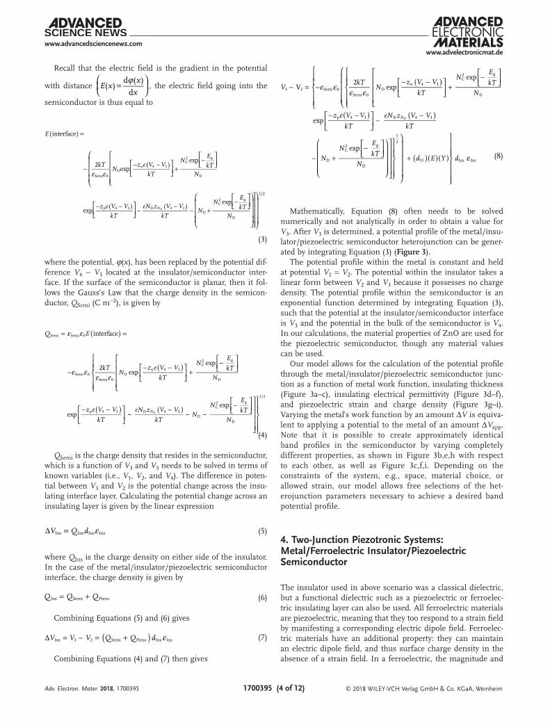
Figure 5a,b shows an n-semiconductor/insulator/p-semi-conductor junction both before and after charge is exchanged between the layers and equilibrium is established across the heterojunction. Potentials V4 through V7 have been added to denote the potential within and across the semiconductor/insu-lator/semiconductor junction. We have neglected piezoelectric and ferroelectric components from this diagram but they may also be added. The diagram shown in Figure 5b, which depicts the energy landscape of the heterojunction in equilibrium, is of a typical form seen in publications and it is often the result of little more than an intuitive guess as to the potential profile across the heterojunction. Unlike the metal/insulator/semi-conductor junction, we must consider the potential gradients on both sides of the insulator to satisfy net neutrality and con-servation of energy. However, all else (e.g., insulator thickness, ferroelectric polarization, piezoelectric charge) may be imple-mented in the same fashion. A more detailed mathematical
argument for this junction is provided in Section S3 (Sup-porting Information).
The potential profiles and energy band diagrams across mul-tiple semiconductor/insulator/semiconductor junctions are shown as a function of insulator thickness (Figure 5c–e) and piezoelectric strain (charge density) on the left semiconductor (Figure 5f–h). Both the semiconductors are treated as having mirrored properties (e.g., equal permittivities and band gaps, equal and oppositely charged dopant densities). The influences of these material parameters can be precisely illustrated by the calculation. Consistent with general semiconductor junc-tion principles, increasing the Fermi level difference between the two semiconductors will increase the band bending (elec-tric field strength) at the interface. Higher dopant density in a semiconductor will lower the percentage of voltage drop occur-ring within that material. Larger electrical permittivity will shift the distribution of potential drop at the interface toward the semiconductor with lower electrical permittivity. As seen from Figure 5c, when the thickness of the insulating layer increases, less band bending will occur within the semiconductors. How-ever, this effect becomes less significant if the insulator has an extremely high relative electrical permittivity (e.g., ≈1500).
High electrical permittivity corresponds to low electric fields, which yields small potential difference even over a relative large thickness. Therefore, for insulators that have high electrical permittivity, the majority of voltage drop will take place within the semiconductors where the fields can be several of orders of magnitude stronger. This also increases the necessary charge to accumulate at either sides of the dielectric. If this charge accu-mulation exceeds the order of magnitude of the piezoelectric charge density, then the effect of piezoelectric polarization becomes less pronounced—hence, the small value of εr,Insulator used for our calculations in Figure 5.
When piezoelectric charge is introduced at the interface, it is distinctly different from the previous cases analyzed. When there are no bulk work function differences and only nonmo-bile piezoelectric charges are introduced at an interface, the only driving force for charge rearrangement in these materials is the lowest energy condition for charge neutrality. In this case, the magnitude of voltage drop in these materials is not a constant but the charge neutrality rule remains a constant. The lower the charge density and electrical permittivity of the materials in contact with the piezoelectric charge, the greater the voltage change across the materials. If there is no insulating layer between the two materials or the insulating layer has a high electrical permittivity, then both the materials will have equal opportunity to screen the piezoelectric charge.
6. Two-Junction Piezotronic Systems: Piezoelectric Semiconductor/Insulator/Solution
The last heterojunctions that we will examine are the piezotronic principles in piezoelectric semiconductor/solution and piezo-electric semiconductor/insulator/solution systems (Figure 6a). These interfaces are studied for use in a wide range of appli-cations, including energy storage (e.g., batteries and capaci-tors), energy conversion (e.g., photo-electrochemical cells), and materials synthesis (e.g., electrochemical deposition).[27,32–46]
Adv. Electron. Mater. 2018, 1700395
www.advancedsciencenews.com
© 2018 WILEY-VCH Verlag GmbH & Co. KGaA, Weinheim1700395 (8 of 12)
www.advelectronicmat.de
Analyzing the semiconductor/insulator/solution interface is similar to the case of the semiconductor/insulator/semicon-ductor heterojunction except that the expression for charge density will no longer depend on material band gaps and the density of immobile, ionized donor atoms as is the case within semiconductors. Instead, it will depend on the concentration, charge, and size of dissolved charged species in solution.
There are three phenomena that one should be vigilant of when preparing a heterojunction with a solution. First, charged species in solution are not point particles like electrons or holes in a semiconductor. Hydrated ions in solution occupy phys-ical space and have a maximum packing density, and thus a
maximum charge density. If a potential difference at the inter-face of a solution is different enough from the potential in the bulk of solution so as to cause an accumulated charge density that exceeds the atomic density of solid matter, then measures need to be taken to prevent this unphysical result from hap-pening (i.e., creating a charged Stern layer). Second, species in solution (atoms, molecules, etc.) can store or release charge through electrochemical reactions, if the potential difference at the interface of a solution is sufficiently large. Third, the solu-tion will react with the solid’s surface, protonating or deproto-nating the surface of the solid (especially metal oxides). This causes the formation of a surface dipole, resulting in a band
Adv. Electron. Mater. 2018, 1700395
Figure 5. Electrical potential profile across a piezoelectric n-type semiconductor/insulator/p-type semiconductor junction. a) Schematic of the energy levels across the heterojunction before equilibrium is established. b) Schematic of the energy band diagram across the heterojunction after charge is allowed to flow and equilibrium is established. c) The effect an insulating layer between the two semiconductors has on the electrical potential distribution in the interface. The dashed lines represent the insulator/p-type semiconductor interface with their corresponding colors to the insulator thicknesses seen in the legend. d,e) Calculated energy band diagrams for an insulator that is 10 and 100 nm thick, respectively. f) The effect strain has on electrical potential in the piezoelectric n-type semiconductor/insulator/p-type semiconductor junction. g,h) Calculated band diagrams for the piezoelectric n-type semiconductor/insulator/p-type semiconductor heterojunction for strain levels of 0.10% and −0.10%, respectively.
www.advancedsciencenews.com
© 2018 WILEY-VCH Verlag GmbH & Co. KGaA, Weinheim1700395 (9 of 12)
www.advelectronicmat.de
shift. The magnitude of the shift can depend on pH, the mate-rial facet exposed to solution, and the activity of ions in solu-tion. Since these practical phenomena are related to specific redox systems, they are not taken into account in our calcula-tion with the exception of the latter.
In order to establishing the conditions in solution, we first need to define the charge density in the solution, which is a func-tion of the solution chemistry. We take 1 m NaOH as an example. For a solution of pure water, the charge concentration ρSolution(x) would be the sum of hydronium (H+) and hydroxide (OH−) ions. Other additional mobile charged species in the form of elec-trolyte may be introduced to the water system. For example, if sodium chloride (NaCl) were added to the solution, the sodium and chloride ion concentrations also need to be included to the total charge density. In every semiconductor/solution junction, an equation for charge density ρSolution(x) will need to be gener-ated, which means that the first step to calculating a heterojunc-tion’s proper electrical potential profile is to determine the chem-ical nature (species and concentrations) of solution.
After a general expression for ρSolution(x) is defined, we next need to know the electrical potential of the bulk solution. In electrochemistry, electrical potentials of solutions are defined by the Nernst equation,[15,47,48] which relates the electrochem-ical potential of a medium (E) to temperature and activity of charged chemical species within the medium as following
E ERT
nF
aa
log010
Ox
Red= − (10)
where E0 is the standard reduction potential for redox couple, R is the universal gas constant, T is the temperature, F is the Faraday constant, n is the number of electrons transferred per oxidation/reduction reaction, aOx and aRed are the activities of the oxidized and reduced species in solution, respectively. E is often given with respect to a reference electrode that is submerged in
solution. When E is referenced to vacuum, it can represent the work function of the bulk solution. This value is needed in our calculations that involve semiconductor or metallic materials whose Fermi levels are already referenced to vacuum energy. With the charge density ρSolution(x) and work function ESolution defined, attention must now be paid to the surface of the semi-conducting material at the solid–solution interface.
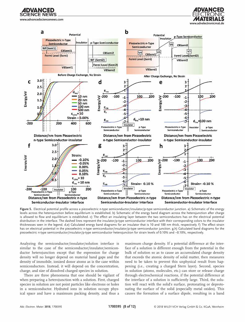
When a solid material is exposed to solution, the surface of the material will exchange atoms with the solution environ-ment until the interface has achieved thermodynamic equi-librium. Since the species in solution are charged ions, the exchange of atoms between the solution and the surface will induce a surface charge. This induced surface charge and its associated countercharge that exists in the vicinity of the inter-face compose a surface dipole that is situated between the bulk of the material and the bulk of the solution. The presence of this surface dipole is a detail often overlooked by casual anal-ysis and yet it can have a dramatic effect on the resultant het-erojunction properties. Here, we take a common piezoelectric semiconductor ZnO as an example and assume that it is p-type for simplicity as well as consistent with our grand scheme shown in Figure S1 (Supporting Information).
The ideal ZnO surface is terminated with the OH groups (Figure 6b).[49,50] When ZnO makes intimate contact with water, OH− and H+ from the solution will chemically interact with the surface of the ZnO, removing H+ from the surface under basic conditions (Figure 6c) or removing OH− from the surface under acidic conditions (Figure 6d). This mechanism causes a relative shift between the Fermi energy of the bulk solid (ZnO) and the Nernst potential of the electrolyte. The pH at which the surface has a net neutral charge is called the isoelectric point (pHiso) and it varies between materials and crystallographic facets of a given material.[35,49–52] As the pH of solution differs from the isoelectric point, a dipole forms at the surface of the material. Figure S5 (Supporting Information) shows the type of
Adv. Electron. Mater. 2018, 1700395
Figure 6. Interface effects at a semiconductor/solution interface. a) Schematic of the material energetics at a semiconductor/insulator/solution het-erojunction prior to charge rearrangement and equilibrium. b) Schematic of a semiconductor (p-type zinc oxide)/solution interface. c,d) The surface of the semiconductor becomes protonated or deprotonated depending on the chemical composition of the solution and the isoelectric point of the semiconductor. This atomic exchange at the interface introduces an electric dipole when the solution conditions are such that they are not equal to the isoelectric point of the semiconductor.
www.advancedsciencenews.com
© 2018 WILEY-VCH Verlag GmbH & Co. KGaA, Weinheim1700395 (10 of 12)
www.advelectronicmat.de
Adv. Electron. Mater. 2018, 1700395
band behavior expected after equilibrium has been established at both the semiconductor/solution interface.
This dipole changes the difference in work function between the semiconductor and the solution and is the cause for the flat-band potential shift that coincides with a change in the pH of solution. In general, the flat-band potential shift with pH (and thus the work function difference as a function of pH) is ≈59 meV per unit of pH change. Therefore, if the Fermi level (EFermi at iso) of the semiconductor relative to solution at the iso-electric point (pHiso) is known, then the Fermi level (EFermi) at any pH can be approximated by[52,53]
E E 0.059 (pH pH )Fermi Fermi at iso iso( )= − × − (11)
We remind the reader that energy levels are given relative to vacuum potential; EFermi and EFermi at iso < 0. The isoelectric point for ZnO has been measured to be between 8.7 and 10.3 depending on substrate, facet, and processing approaches.[54] In our calculation, we take pHiso = 9.5. After accounting for the adjustment to work function difference that comes through the pH-sensitive surface dipole phenomena, the calculation of the
heterojunction electrical potential profile can proceed as dis-cussed in previous sections.
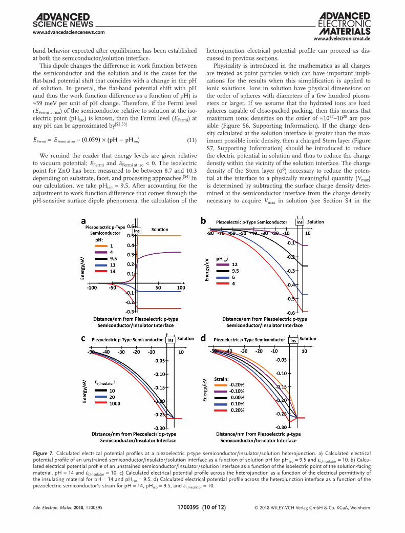
Physicality is introduced in the mathematics as all charges are treated as point particles which can have important impli-cations for the results when this simplification is applied to ionic solutions. Ions in solution have physical dimensions on the order of spheres with diameters of a few hundred picom-eters or larger. If we assume that the hydrated ions are hard spheres capable of close-packed packing, then this means that maximum ionic densities on the order of ≈1027–1028 are pos-sible (Figure S6, Supporting Information). If the charge den-sity calculated at the solution interface is greater than the max-imum possible ionic density, then a charged Stern layer (Figure S7, Supporting Information) should be introduced to reduce the electric potential in solution and thus to reduce the charge density within the vicinity of the solution interface. The charge density of the Stern layer (σS) necessary to reduce the poten-tial at the interface to a physically meaningful quantity (Vmax) is determined by subtracting the surface charge density deter-mined at the semiconductor interface from the charge density necessary to acquire Vmax in solution (see Section S4 in the
Figure 7. Calculated electrical potential profiles at a piezoelectric p-type semiconductor/insulator/solution heterojunction. a) Calculated electrical potential profile of an unstrained semiconductor/insulator/solution interface as a function of solution pH for pHiso = 9.5 and εr,Insulator = 10. b) Calcu-lated electrical potential profile of an unstrained semiconductor/insulator/solution interface as a function of the isoelectric point of the solution-facing material, pH = 14 and εr,Insulator = 10. c) Calculated electrical potential profile across the heterojunction as a function of the electrical permittivity of the insulating material for pH = 14 and pHiso = 9.5. d) Calculated electrical potential profile across the heterojunction interface as a function of the piezoelectric semiconductor’s strain for pH = 14, pHiso = 9.5, and εr,Insulator = 10.
www.advancedsciencenews.com
© 2018 WILEY-VCH Verlag GmbH & Co. KGaA, Weinheim1700395 (11 of 12)
www.advelectronicmat.de
Adv. Electron. Mater. 2018, 1700395
Supporting Information). If a Stern layer is a necessary addi-tion to the calculation, then depending on the length scales of interest, it may be important to include the physical thickness of the Stern layer in the electrical potential diagram, which will be the hydration diameter of ions comprising the Stern layer.
We demonstrate the effect of changing the pH of solution (Figure 7a), the isoelectric point of the solution-facing mate-rial (Figure 7b), insulating layer’s permittivity (Figure 7c), and strain of the piezoelectric semiconductor (Figure 7d) on the het-erojunction potential profiles. The direction of band bending at the semiconductor/insulator interface in Figure 7a–d depends both on the value of the semiconductor’s Fermi level relative to work function of solution, as governed by the Nernst equation (Figure 7a–d) and the ferroelectric or piezoelectric charge den-sity introduced at the interface (Figure 7d).
The amount of charge accumulation (or depletion) in the semiconductor increases as we increase the difference between V7 and V10 (i.e., the difference between pH and pHiso) and the value εIns. As such, this charge may be of magnitudes higher than that of the piezoelectric charge density which removes the effectiveness of a piezoelectric. Our calculations use somewhat low values of εIns and differences in pH and pHiso to emphasize the effect that ZnO piezoelectric polarization can have. Using other high performance piezoelectric/ferroelectric material, such as SrTiO3 or Pb[ZrxTi1−x]O3, the piezoelectric polarization influence may be raised.[27,55]
All the explored variables show effects of band bending in the semiconductor within a magnitude of order (tens to hun-dreds of meV). This demonstrates that each of these variables may be used to make a considerable modification to the junc-tion’s potential profile. Given the conditions given by a device and its use, and physical limits of the materials used therein, one may explore different pathways of exploiting these vari-ables to optimize their device’s energy landscape.
7. Conclusion
In this paper, we explained the scientific basis for a model that is able to plot heterojunctions of materials with different length scales and varying dielectric, piezoelectric, electrical, and chemical properties. The model for metal/semiconductor and semiconductor/semiconductor heterojunctions will effec-tively generate potential profiles that are useful to quantitatively explain the electronic behaviors of corresponding heterojunc-tion devices. The inclusion of ferroelectric and piezoelectric properties to both the insulator and the semiconductor reveals the effect of strain and ferroelectric polarization on the perfor-mance of those devices. The relevant band structures provide the core principle of the piezotronic systems. These models will be increasingly useful as more piezoelectric and ferroelectric materials are investigated for their photovoltaic or optoelec-tronic properties. The semiconductor/solution heterojunctions have become the foci of fervent activity as photo-electrochem-ical cells, batteries, and capacitors have become hot topics of scientific interests. Our model takes into account the isoelectric point of the surface making contact with solution and adjusts the relevant material parameters accordingly. The inclusion of ferroelectric and piezoelectric material properties into these
junctions directs the piezotronic concept into these electrochem-istry systems, offering a new guide for engineering the behavior of these interfaces. The code used to produce the calculated band diagrams within this paper will provide a quantitative guideline for predicting the implementation of the piezotronic effect in many state-of-the-art heterojunction devices to engineer the material junctions and improve their performance.
Supporting InformationSupporting Information is available from the Wiley Online Library or from the author.
AcknowledgementsL.N.G. and M.B.S. contributed equally to this work. This work was supported by the National Science Foundation under Award #CMMI-1148919.
Conflict of InterestThe authors declare no conflict of interest.
Keywordselectrochemistry, heterojunction energetics, piezoelectrics, piezotronics
Received: August 21, 2017Revised: November 19, 2017
Published online:
[1] F. Braun, Ann. Phys. Chem. 1875, 229, 556.[2] Internet Archive, Braun, http://web.archive.org/web/20060211010305/
http://chem.ch.huji.ac.il/~eugeniik/history/braun.htm (accessed: August 2016).
[3] F. Guthrie, Philos. Mag. 1894, 17, 462.[4] O. W. Richardson, Thermionic Phenomena and the Laws which
Govern Them, http://www.nobelprize.org/nobel_prizes/physics/laureates/1928/richardson-lecture.pdf (accessed: August 2016).
[5] E. Seale, Diode, http://encyclobeamia.solarbotics.net/articles/diode.html (accessed: August 2016).
[6] Y. M. Wong, W. P. Kang, J. L. Davidson, A. Wisitsora-at, K. L. Soh, Sens. Actuators, B 2003, 93, 327.
[7] K.-P. Hsueh, C.-T. Pan, C.-T. Li, H.-C. Lin, Y.-M. Hsin, J.-I. Chyi, J. Electrochem. Soc. 2010, 157, H381.
[8] Z. L. Wang, Adv. Mater. 2012, 24, 4632.[9] R. E. Hummel, Electronic Properties of Materials, Springer, New York,
NY 2011.[10] S. M. Sze, K. K. Ng, Physics of Semiconductor Devices, John Wiley
and Sons, Hoboken, NJ 2007.[11] C. C. Hu, Modern Semiconductor Devices for Integrated Circuits,
Pearson, Upper Saddle River, NJ 2009.[12] A. Hadipour, B. de Boer, P. Blom, Adv. Funct. Mater. 2008, 18, 169.[13] A. Martí, A. Luque, Nat. Commun. 2015, 6, 6902.[14] H. Morkoç, S. Strite, G. B. Gao, M. E. Lin, B. Sverdlov, M. Burns,
J. Appl. Phys. 1994, 76, 1363.[15] X.-H. Zhang, B. Domercq, X. Wang, S. Yoo, T. Kondo, Z. L. Wang,
B. Kippelen, Org. Electron. 2007, 8, 718.
www.advancedsciencenews.com
© 2018 WILEY-VCH Verlag GmbH & Co. KGaA, Weinheim1700395 (12 of 12)
www.advelectronicmat.de
Adv. Electron. Mater. 2018, 1700395
[16] X. Wang, J. Zhou, J. Song, J. Liu, N. Xu, Z. L. Wang, Nano Lett. 2006, 6, 2768.
[17] Y. Yu, J. Li, D. Geng, J. Wang, L. Zhang, T. L. Andrew, M. S. Arnold, X. Wang, ACS Nano 2015, 9, 564.
[18] Z. L. Wang, R. Yang, J. Zhou, Y. Qin, C. Xu, Y. Hu, S. Xu, Mater. Sci. Eng., R 2010, 70, 320.
[19] Z. L. Wang, Nano Today 2010, 5, 540.[20] W. Wu, L. Wang, Y. Li, F. Zhang, L. Lin, S. Niu, D. Chenet, X. Zhang,
Y. Hao, T. F. Heinz, J. Hone, Z. L. Wang, Nature 2014, 514, 470.[21] Z. Liu, M. Kobayashi, B. C. Paul, Z. Bao, Y. Nishi, in 2009 IEEE
Int. Electron Devices Meeting (IEDM), IEEE, Piscataway, NJ 2009, pp. 379–382.
[22] Z. Liu, M. Kobayashi, B. C. Paul, Z. Bao, Y. Nishi, Phys. Rev. B 2010, 82, 035311.
[23] M. Kobayashi, A. Kinoshita, K. Saraswat, H. S. P. Wong, Y. Nishi, in 2008 Symp. on VLSI Technology, IEEE, Piscataway, NJ 2008, pp. 54–55.
[24] K.-Y. Chen, C.-C. Su, C.-P. Chou, Y.-H. Wu, IEEE Electron Device Lett. 2016, 37, 827.
[25] W. Mönch, J. Appl. Phys. 2012, 111, 073706.[26] Y. Cui, J. Briscoe, S. Dunn, Chem. Mater. 2013, 25, 4215.[27] W. Yang, Y. Yu, M. B. Starr, X. Yin, Z. Li, A. Kvit, S. Wang, P. Zhao,
X. Wang, Nano Lett. 2015, 15, 7574.[28] P. Yilmaz, D. Yeo, H. Chang, L. Loh, S. Dunn, Nanotechnology 2016,
27, 345402.[29] L. Loh, J. Briscoe, S. Dunn, Nanoscale 2014, 6, 7072.[30] M. R. Morris, S. R. Pendlebury, J. Hong, S. Dunn, J. R. Durrant, Adv.
Mater. 2016, 28, 7123.[31] B. Chen, J. Shi, X. Zheng, Y. Zhou, K. Zhu, S. Priya, J. Mater. Chem.
A 2015, 3, 7699.[32] Z. Li, C. Yao, Y. Yu, Z. Cai, X. Wang, Adv. Mater. 2014, 26, 2262.[33] Y. Chen, K. Sun, H. Audesirk, C. Xiang, N. S. Lewis, Energy Environ.
Sci. 2015, 8, 1736.[34] F. Wang, W. Xiao, L. Gao, G. Xiao, Catal. Sci. Technol. 2016, 6, 3074.[35] Y. Sun, D. Riley, M. N. R. Ashfold, J. Phys. Chem. B 2006, 110, 15186.
[36] J. Shi, X. Wang, Energy Environ. Sci. 2012, 5, 7918.[37] J. Shi, Y. Hara, C. Sun, M. A. Anderson, X. Wang, Nano Lett. 2011,
11, 3413.[38] M. B. Starr, X. Wang, Nano Energy 2015, 14, 296.[39] J. Shi, M. B. Starr, X. Wang, Adv. Mater. 2012, 24, 4683.[40] M. B. Starr, X. Wang, Sci. Rep. 2013, 3, 2160.[41] Z. Li, C. Yao, F. Wang, Z. Cai, X. Wang, Nanotechnology 2014, 25,
504005.[42] H. Li, Y. Yu, M. B. Starr, Z. Li, X. Wang, J. Phys. Chem. Lett. 2015, 6,
3410.[43] Z. Zhang, Q. Liao, Y. Yu, X. Wang, Y. Zhang, Nano Energy 2014, 9,
237.[44] Y. Chen, S. Hu, C. Xiang, N. S. Lewis, Energy Environ. Sci. 2015, 8,
876.[45] N. T. Plymale, A. A. Ramachandran, A. Lim, B. S. Brunschwig,
N. S. Lewis, J. Phys. Chem. C 2016, 120, 14157.[46] M. F. Lichterman, K. Sun, S. Hu, X. Zhou, M. T. McDowell,
M. R. Shaner, M. H. Richter, E. J. Crumlin, A. I. Carim, F. H. Saadi, B. S. Brunschwig, N. S. Lewis, Catal. Today 2016, 262, 11.
[47] K. W. Johnston, A. G. Pattantyus-Abraham, J. P. Clifford, S. H. Myrskog, S. Hoogland, H. Shukla, E. J. D. Klem, L. Levina, E. H. Sargent, Appl. Phys. Lett. 2008, 92, 122111.
[48] L. Hong-Xia, G. Bo, Z. Qing-Qing, W. Yong-Huai, Acta Phys. Sin. 2012, 61, 057802.
[49] J. Hüpkes, J. I. Owen, S. E. Pust, E. Bunte, ChemPhysChem 2012, 13, 66.
[50] M. Valtiner, S. Borodin, G. Grundmeier, Phys. Chem. Chem. Phys. 2007, 9, 2406.
[51] B. Meyer, Phys. Rev. B 2004, 69, 045416.[52] G. A. Parks, Chem. Rev. 1965, 65, 177.[53] C. F. Zinola, Electrocatalysis: Computational, Experimental, and Indus-
trial Aspects, CRC Press, Boca Raton, FL 2010.[54] M. A. Butler, D. S. Ginley, J. Electrochem. Soc. 1978, 125, 228.[55] F. Wu, Y. Yu, H. Yang, L. N. German, Z. Li, J. Chen, W. Yang,
L. Huang, W. Shi, L. Wang, X. Wang, Adv. Mater. 2017, 29, 1701432.