computer organization and architecture william stallings 8th edition chapter 2 computer evolution...
TRANSCRIPT

Computer Organization and Architecture
William Stallings 8th Edition
Chapter 2Computer Evolution and
Performance
BRIEF HISTORY OF COMPUTERS
The First Generation: Vacuum Tubes

ENIAC - background•Electronic Numerical Integrator And
Computer•Eckert and Mauchly proposed to build a
general-purpose computer using vacuum tubes for the BRL’s application.
•At university of Pennsylvania•It was the world’s first general purpose
electronic digital computer.•Started 1943•Finished 1946
▫Too late for war effort•Used until 1955
ENIAC - details•The ENIAC was a decimal rather than a
binary machine. Numbers were represented in decimal form, and arithmetic was performed in the decimal system.
•Its memory consisted of 20 accumulators of 10 digits number.
•It had to be programmed manually by setting switches and plugging and unplugging cables.
•The resulting machine was enormous, weighing 30 tons, occupying 1500 square feet of floor space, and containing more than 18,000 vacuum tubes.

ENIAC - details•When operating, it consumed 140 kilowatts of
power.
•It was also substantially faster than any electromechanical computer, capable of 5000 additions per second.
Von Neumann/Turing
•The idea is a computer could get its instructions by reading them from memory, and a program could be set or altered by setting the values of a portion of memory.
•This idea, known as the stored-program concept.
•The first publication of the idea was in a 1945 proposal by von Neumann for a new computer, the EDVAC (Electronic Discrete Variable Computer).
Von Neumann/Turing• In 1946, von Neumann and his colleagues began
the design of a new stored program computer, referred to as the IAS computer, at the Princeton Institute for Advanced Studies.
• The general structure of the IAS computer consists of:▫Main memory stores data and instructions1
▫Arithmetic and logic unit (ALU) capable of operating on binary data.
▫Control unit (CU) interprets instructions in memory to be executed.
▫Input and output (I/O) equipment operated by the control unit.
•Completed 1952.

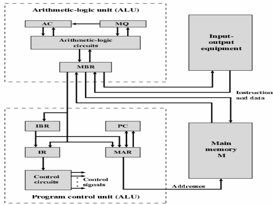
Structure of The IAS Computer

• all of today’s computers have this same general structure and function and are thus referred to as von Neumann machines.
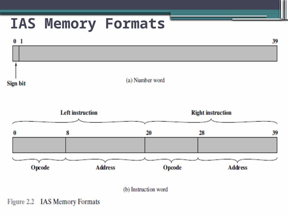
IAS Memory Formats:• The memory of the IAS consists of 1000 storage
locations, called words, of 40 binary digits (bits) each.• Both data and instructions are stored there. • Numbers are represented in binary form, and each
instruction is a binary code. • Each number is represented by a sign bit and a 39-bit
value.• A word may also contain two 20-bit instructions, with
each instruction consisting of an 8-bit operation code (opcode) specifying the operation to be performed and a 12-bit address designating one of the words in memory (numbered from 0 to 999).
IAS Memory Formats

Structure of IAS Computer•The control unit operates the IAS by fetching
instructions from memory and executing them one at a time.
•Both the control unit and the ALU contain storage locations, called registers, defined as follows:
Memory buffer register (MBR). Memory address register (MAR). Instruction register (IR). Instruction buffer register (IBR). Program counter (PC). Accumulator (AC) and multiplier quotient (MQ)
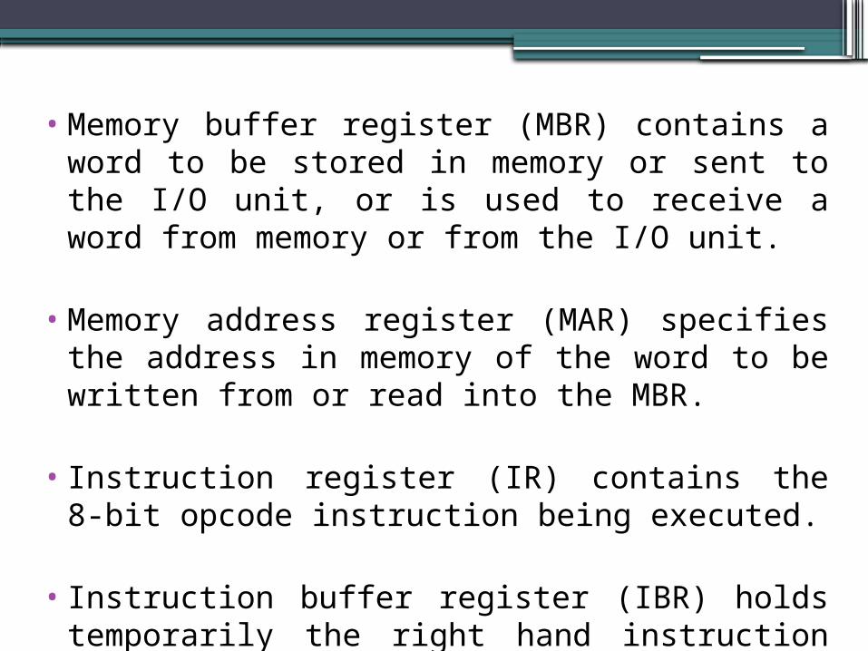
• Memory buffer register (MBR) contains a word to be stored in memory or sent to the I/O unit, or is used to receive a word from memory or from the I/O unit.
• Memory address register (MAR) specifies the address in memory of the word to be written from or read into the MBR.
• Instruction register (IR) contains the 8-bit opcode instruction being executed.
• Instruction buffer register (IBR) holds temporarily the right hand instruction from a word in memory.
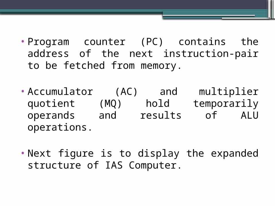
• Program counter (PC) contains the address of the next instruction-pair to be fetched from memory.
• Accumulator (AC) and multiplier quotient (MQ) hold temporarily operands and results of ALU operations.
• Next figure is to display the expanded structure of IAS Computer.

IAS - details•1000 x 40 bit words
▫Binary number▫2 x 20 bit instructions
•Set of registers (storage in CPU)▫Memory Buffer Register▫Memory Address Register▫Instruction Register▫Instruction Buffer Register▫Program Counter▫Accumulator▫Multiplier Quotient
•The IAS operates by repetitively performing an instruction cycle, each instruction cycle consists of two subcycles: fetch cycle and execution cycle.

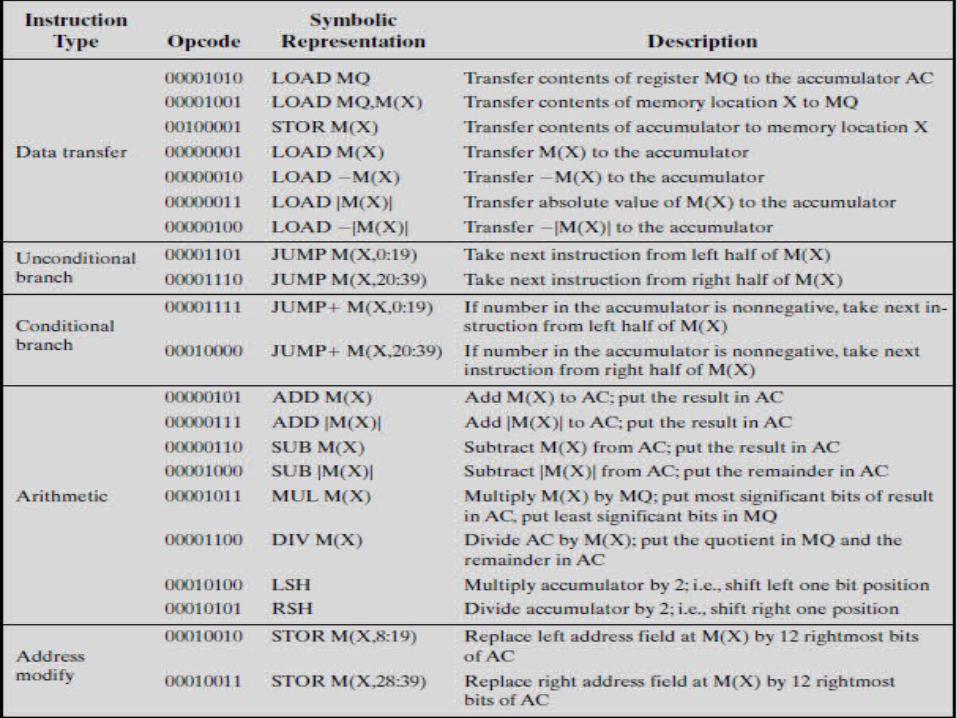
IAS Computer Instructions• The IAS computer had a total of 21 instructions, which are
grouped as follows: • Data transfer: Move data between memory and ALU registers or
between two ALU registers.
• Unconditional branch: Normally, the control unit executes instructions in sequence from memory. This sequence can be changed by a branch instruction, which facilitates repetitive operations.
• Conditional branch: The branch can be made dependent on a condition, thus allowing decision points.
• Arithmetic: Operations performed by the ALU.
• Address modify: Permits addresses to be computed in the ALU and then inserted into instructions stored in memory. This allows a program considerable addressing flexibility.

Commercial Computers
• In1947, Eckert and Mauchly formed the Eckert-Mauchly Computer Corporation to manufacture computers commercially.
• It was called UNIVAC I (Universal Automatic Computer) as the first successful commercial computer.
• In the late 1950s, the UNIVAC II was delivered which had greater memory capacity and higher performance than the UNIVAC I.
• UNIVAC II is faster and it has more memory.
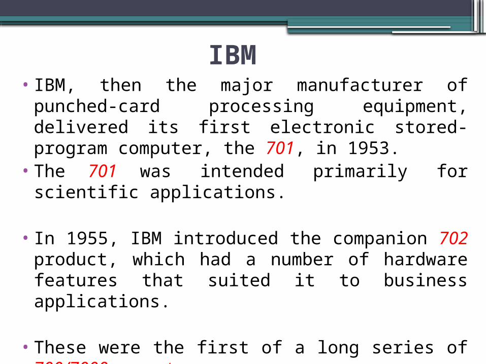
IBM• IBM, then the major manufacturer of punched-card
processing equipment, delivered its first electronic stored-program computer, the 701, in 1953.
• The 701 was intended primarily for scientific applications.
• In 1955, IBM introduced the companion 702 product, which had a number of hardware features that suited it to business applications.
• These were the first of a long series of 700/7000 computers.

The Second GenerationTransistors
• The first major change in the electronic computer came with the replacement of the vacuum tube by the transistor.
• The transistor is smaller, cheaper, and dissipates less heat than a vacuum tube, but can be used in the same way as a vacuum tube to construct computers.
• Unlike the vacuum tube, which requires wires, metal plates, a glass capsule, and a vacuum, the transistor is a solid-state device, made from silicon.
• It was invented in 1947 at Bell Labs.

Transistor Based Computers
• The use of the transistor defines the second generation of computers.
• IBM again was not the first company to deliver the new technology. NCR and RCA were the front-runners with some small transistor machines.
• IBM followed shortly with the 7000 series.• The second generation is noteworthy also for the appearance
of the Digital Equipment Corporation (DEC).• DEC was founded in 1957 and, in that year, delivered its
first computer which is called the PDP-1.

The Third GenerationIntegrated Circuits - Microelectronics
• In 1958 came the achievement that revolutionized electronics and started the era of microelectronics: the invention of the integrated circuit.
• It is the integrated circuit that defines the third generation of computers.
• Microelectronics means “small electronics.” • Since the beginnings of digital electronics and the
computer industry, there has been a persistent and consistent trend toward the reduction in size of digital electronic circuits.
• A computer is made up of gates, memory cells and interconnections.
The Third GenerationIntegrated Circuits - Microelectronics
• These can be manufactured on a semiconductor e.g. silicon wafer.
• The basic elements of a digital computer must perform storage, movement, processing, and control functions. Only two fundamental types of components are required: gates and memory cells.
• A gate is a device that implements a simple boolean or logical function such as (AND gate).
• The memory cell is a device that can store one bit of data. • By interconnecting large numbers of these fundamental
devices, we can construct a computer.
• We can relate this to our four basic functions as follows:▫Data storage: Provided by memory cells.▫Data processing: Provided by gates.▫Data movement: The paths among components are used to
move data from memory to memory and from memory through gates to memory.
▫Control: The paths among components can carry control signals.

Fundamental Computer Elements

Generations of Computer
• Vacuum tube - 1946-1957• Transistor - 1958-1964• Small scale integration - 1965
▫Up to 100 devices on a chip• Medium scale integration - to 1971
▫100-3,000 devices on a chip• Large scale integration (LSI) - 1971-1977
▫3,000 - 100,000 devices on a chip• Very large scale integration (VLSI) - 1978 -1991
▫100,000 - 100,000,000 devices on a chip• Ultra large scale integration (ULSI) - 1991
▫Over 100,000,000 devices on a chip

Moore’s Law
• Increased density of components on chip.• Gordon Moore – cofounder of Intel.• Number of transistors on a chip will double every year.• Since 1970’s development has slowed a little.
▫Number of transistors doubles every 18 months.• Cost of a chip has remained almost unchanged.• Higher packing density means shorter electrical paths, giving
higher performance.• Smaller size gives increased flexibility.• Reduced power and cooling requirements.• Fewer interconnections increases reliability.

Growth in CPU Transistor Count
This figure reflects the famous Moore’s law.
IBM 360 series• In 1964, IBM announced the System/360, a new family of
computer products. • It was replaced and not compatible with 7000 series, so the 360
product line was incompatible with older IBM machines. • First planned “family” of computers, the characteristics of the
family are as follows :▫ Similar or identical instruction sets.▫ Similar or identical O/S.▫ Increasing speed.▫ Increasing number of I/O ports (i.e. more terminals).▫ Increased memory size.▫ Increased cost.
• Multiplexed switch structure.
DEC PDP-8
• In1964, PDP-8 was appeared from Digital Equipment Corporation (DEC).
• Small size and low cost.• First minicomputer (after miniskirt!).• Did not need air conditioned room.• Small enough to sit on a lab bench.• Cost $16,000, it was cheap enough for each lab
technician to have one.▫$100k+ for IBM 360
• Embedded applications and original equipment manufacturers (OEM).
• Used bus structure.

DEC - PDP-8 Bus Structure
• The PDP-8 bus, called the Omnibus, consists of 96 separate signal paths, used to carry control, address, and data signals.
Later Generations Semiconductor Memory
• In 1970, Fairchild produced the first relatively capacious semiconductor memory.
• It was about the size of a single core.▫i.e. 1 bit of magnetic core storage.
• It holds 256 bits of memory.•Non-destructive read.•Much faster than core.•Capacity approximately doubles each year.

MICROPROCESSORS -Intel
•1971 – Intel 4004 ▫First microprocessor.▫All CPU components on a single chip.▫4-bit microprocessor.▫Designed for specific applications.
•1972 - Intel 8008▫8-bit microprocessor.▫Designed for specific applications.▫Twice as complex as the 4004.
MICROPROCESSORS -Intel
•1974 - 8080▫Intel’s first general purpose microprocessor.▫Designed to be the CPU of a general-purpose microcomputer.▫8-bit microprocessor.▫Faster.▫Has a richer instruction set.▫Has a large addressing capability.
•At the end of 1970s – 8086▫General-purpose.▫16-bit microprocessor.
•1985- 80386▫32-bit microprocessor.
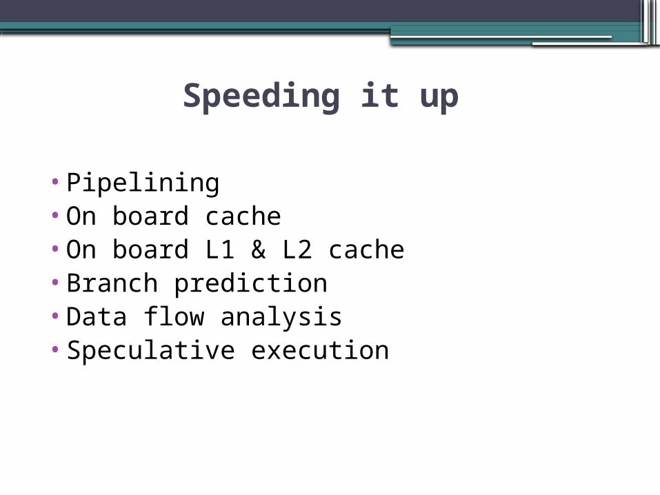
Speeding it up
•Pipelining•On board cache•On board L1 & L2 cache•Branch prediction•Data flow analysis•Speculative execution
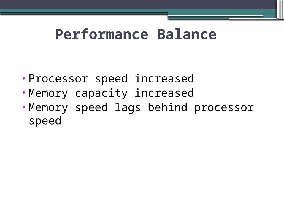
Performance Balance
•Processor speed increased•Memory capacity increased•Memory speed lags behind processor speed
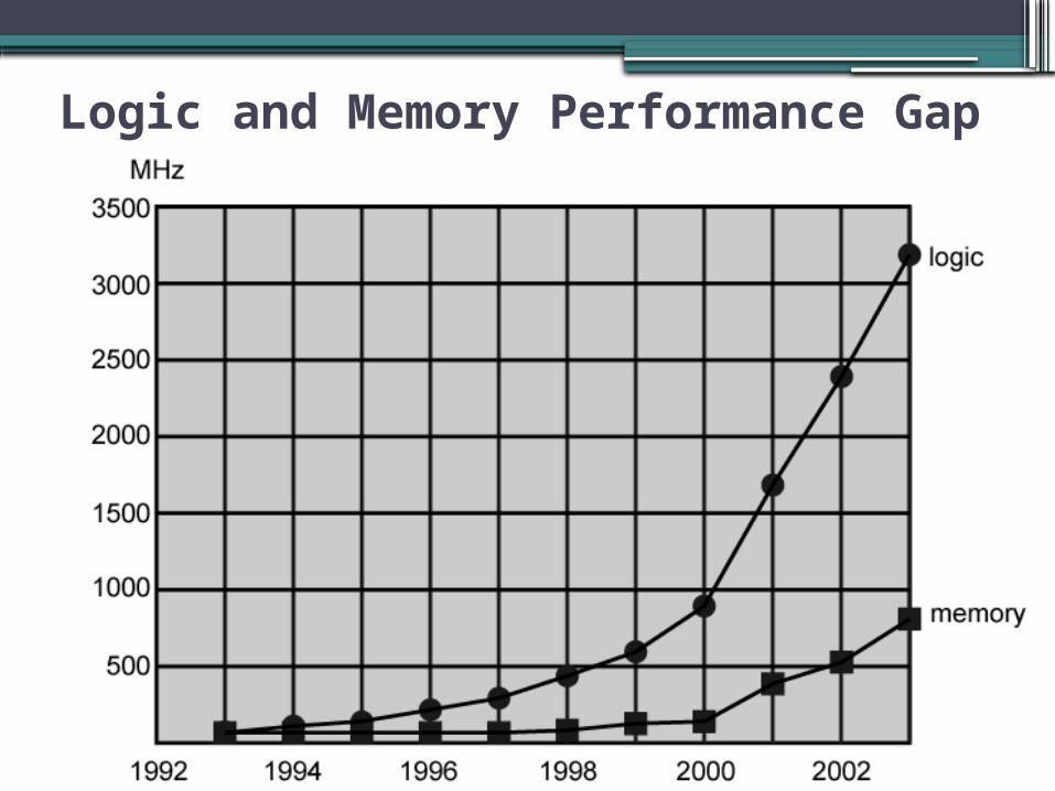
Logic and Memory Performance Gap
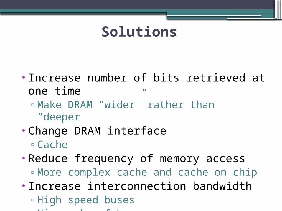
Solutions
• Increase number of bits retrieved at one time▫Make DRAM “wider” rather than “deeper”
•Change DRAM interface▫Cache
•Reduce frequency of memory access▫More complex cache and cache on chip
• Increase interconnection bandwidth▫High speed buses▫Hierarchy of buses

I/O Devices
•Peripherals with intensive I/O demands•Large data throughput demands•Processors can handle this•Problem moving data •Solutions:
▫Caching▫Buffering▫Higher-speed interconnection buses▫More elaborate bus structures▫Multiple-processor configurations
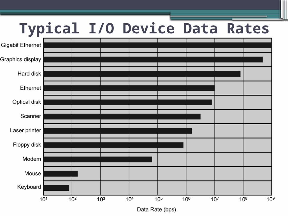
Typical I/O Device Data Rates

Key is Balance
•Processor components•Main memory• I/O devices• Interconnection structures

Improvements in Chip Organization and Architecture
• Increase hardware speed of processor▫Fundamentally due to shrinking logic gate size
More gates, packed more tightly, increasing clock rate Propagation time for signals reduced
• Increase size and speed of caches▫Dedicating part of processor chip
Cache access times drop significantly
•Change processor organization and architecture▫Increase effective speed of execution▫Parallelism
Problems with Clock Speed and Login Density
• Power▫ Power density increases with density of logic and clock speed▫ Dissipating heat
• RC delay▫ Speed at which electrons flow limited by resistance and capacitance of metal
wires connecting them▫ Delay increases as RC product increases▫ Wire interconnects thinner, increasing resistance▫ Wires closer together, increasing capacitance
• Memory latency▫ Memory speeds lag processor speeds
• Solution:▫ More emphasis on organizational and architectural approaches

Intel Microprocessor Performance
Increased Cache Capacity
•Typically two or three levels of cache between processor and main memory
•Chip density increased▫More cache memory on chip
Faster cache access
•Pentium chip devoted about 10% of chip area to cache
•Pentium 4 devotes about 50%
More Complex Execution Logic
•Enable parallel execution of instructions•Pipeline works like assembly line
▫Different stages of execution of different instructions at same time along pipeline
•Superscalar allows multiple pipelines within single processor▫Instructions that do not depend on one another can be
executed in parallel

Diminishing Returns
• Internal organization of processors complex▫Can get a great deal of parallelism▫Further significant increases likely to be relatively
modest•Benefits from cache are reaching limit• Increasing clock rate runs into power dissipation
problem ▫Some fundamental physical limits are being reached

New Approach – Multiple Cores
• Multiple processors on single chip▫ Large shared cache
• Within a processor, increase in performance proportional to square root of increase in complexity
• If software can use multiple processors, doubling number of processors almost doubles performance
• So, use two simpler processors on the chip rather than one more complex processor
• With two processors, larger caches are justified▫ Power consumption of memory logic less than processing logic
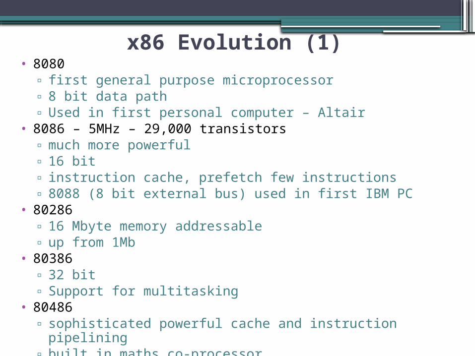
x86 Evolution (1)• 8080
▫ first general purpose microprocessor▫ 8 bit data path▫ Used in first personal computer – Altair
• 8086 – 5MHz – 29,000 transistors▫ much more powerful▫ 16 bit▫ instruction cache, prefetch few instructions▫ 8088 (8 bit external bus) used in first IBM PC
• 80286▫ 16 Mbyte memory addressable▫ up from 1Mb
• 80386▫ 32 bit▫ Support for multitasking
• 80486▫ sophisticated powerful cache and instruction pipelining▫ built in maths co-processor

x86 Evolution (2)• Pentium
▫ Superscalar▫ Multiple instructions executed in parallel
• Pentium Pro▫ Increased superscalar organization▫ Aggressive register renaming▫ branch prediction▫ data flow analysis▫ speculative execution
• Pentium II▫ MMX technology▫ graphics, video & audio processing
• Pentium III▫ Additional floating point instructions for 3D graphics
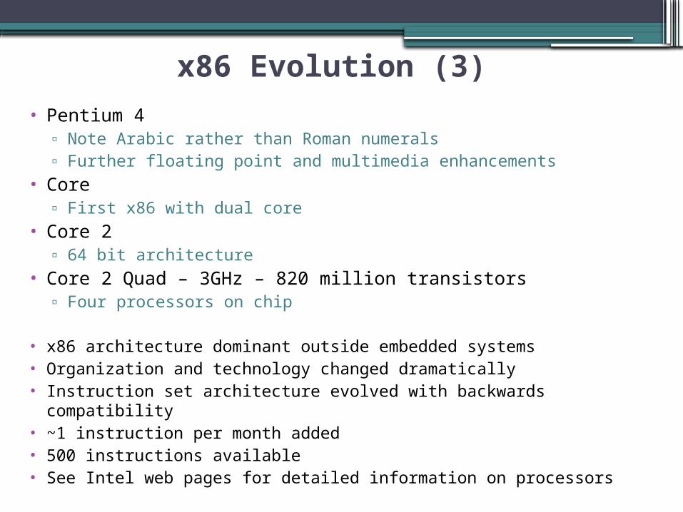
x86 Evolution (3)
• Pentium 4▫ Note Arabic rather than Roman numerals▫ Further floating point and multimedia enhancements
• Core▫ First x86 with dual core
• Core 2▫ 64 bit architecture
• Core 2 Quad – 3GHz – 820 million transistors▫ Four processors on chip
• x86 architecture dominant outside embedded systems• Organization and technology changed dramatically• Instruction set architecture evolved with backwards compatibility• ~1 instruction per month added• 500 instructions available• See Intel web pages for detailed information on processors

Embedded Systems ARM
• Embedded system. A combination of computer hardware and software, and perhaps additional mechanical or other parts, designed to perform a dedicated function. In many cases, embedded systems are part of a larger system or product.
• An alternative approach to processor design in the reduced instruction set computer (RISC).
• The ARM architecture is used in a wide variety of embedded systems and is one of the most powerful and best-designed RISC-based systems on the market.
Embedded Systems ARM
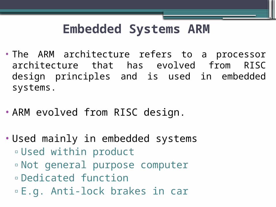
• The ARM architecture refers to a processor architecture that has evolved from RISC design principles and is used in embedded systems.
• ARM evolved from RISC design. • Used mainly in embedded systems
▫Used within product▫Not general purpose computer▫Dedicated function▫E.g. Anti-lock brakes in car

Embedded Systems Requirements
•Different sizes▫Different constraints, optimization, reuse
•Different requirements▫Safety, reliability, real-time, flexibility, legislation▫Lifespan▫Environmental conditions▫Static v dynamic loads▫Slow to fast speeds▫Computation v I/O intensive▫Discrete event v continuous dynamics
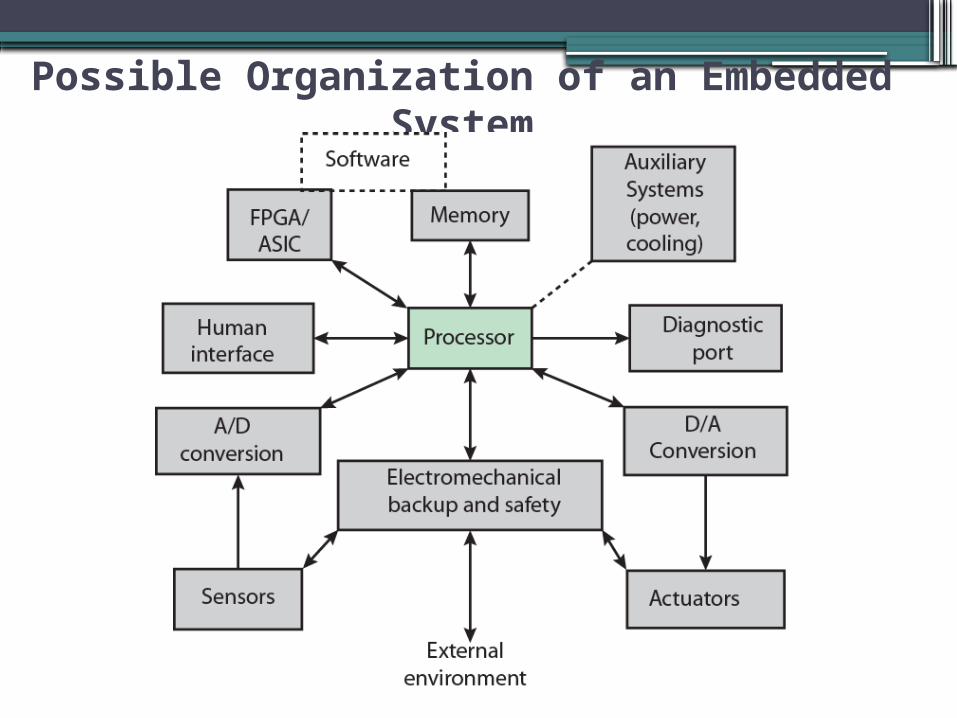
Possible Organization of an Embedded System
ARM Evolution
•Designed by ARM Inc., Cambridge, England•Licensed to manufacturers•High speed, small die, low power consumption•PDAs, hand held games, phones
▫E.g. iPod, iPhone•Acorn produced ARM1 & ARM2 in 1985 and ARM3
in 1989•Acorn, VLSI and Apple Computer founded ARM
Ltd.

ARM Systems Categories
•Embedded real time•Application platform
▫Linux, Palm OS, Symbian OS, Windows mobile•Secure applications
Performance AssessmentClock Speed
• Key parameters▫ Performance, cost, size, security, reliability, power consumption
• System clock speed▫ In Hz or multiples of▫ Clock rate, clock cycle, clock tick, cycle time
• Signals in CPU take time to settle down to 1 or 0• Signals may change at different speeds• Operations need to be synchronised• Instruction execution in discrete steps
▫ Fetch, decode, load and store, arithmetic or logical▫ Usually require multiple clock cycles per instruction
• Pipelining gives simultaneous execution of instructions• So, clock speed is not the whole story
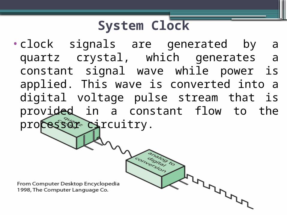
System Clock•clock signals are generated by a quartz crystal, which
generates a constant signal wave while power is applied. This wave is converted into a digital voltage pulse stream that is provided in a constant flow to the processor circuitry.

Instruction Execution Rate
•Millions of instructions per second (MIPS)•Millions of floating point instructions per second
(MFLOPS)•Heavily dependent on instruction set, compiler
design, processor implementation, cache & memory hierarchy

Benchmarks
• Programs designed to test performance• Written in high level language
▫ Portable • Represents style of task
▫ Systems, numerical, commercial• Easily measured• Widely distributed• E.g. System Performance Evaluation Corporation (SPEC)
▫ CPU2006 for computation bound 17 floating point programs in C, C++, Fortran 12 integer programs in C, C++ 3 million lines of code
▫ Speed and rate metrics Single task and throughput

SPEC Speed Metric
• Single task• Base runtime defined for each benchmark using reference
machine• Results are reported as ratio of reference time to system run
time▫ Trefi execution time for benchmark i on reference machine▫ Tsuti execution time of benchmark i on test system
• Overall performance calculated by averaging ratios for all 12 integer benchmarks—Use geometric mean
– Appropriate for normalized numbers such as ratios
, , ∏xi = x1∙x2∙...∙xn

SPEC Rate Metric
• Measures throughput or rate of a machine carrying out a number of tasks
• Multiple copies of benchmarks run simultaneously▫Typically, same as number of processors
• Ratio is calculated as follows:▫Trefi reference execution time for benchmark i▫N number of copies run simultaneously▫Tsuti elapsed time from start of execution of program
on all N processors until completion of all copies of program
▫Again, a geometric mean is calculated
Amdahl’s Law
• Gene Amdahl [AMDA67]• Potential speed up of program using multiple processors• Concluded that:
▫Code needs to be parallelizable▫Speed up is bound, giving diminishing returns for more
processors• Task dependent
▫Servers gain by maintaining multiple connections on multiple processors
▫Databases can be split into parallel tasks
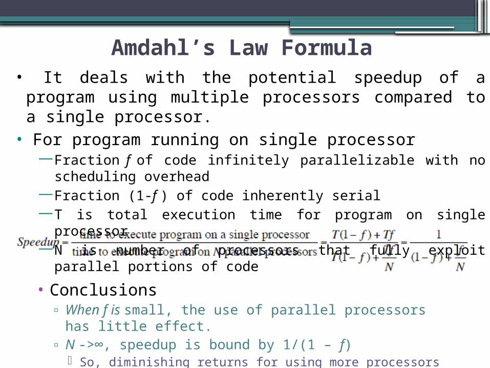
Amdahl’s Law Formula
• Conclusions▫ When f is small, the use of parallel processors has little effect.▫ N ->∞, speedup is bound by 1/(1 – f)
So, diminishing returns for using more processors
• It deals with the potential speedup of a program using multiple processors compared to a single processor.• For program running on single processor
—Fraction f of code infinitely parallelizable with no scheduling overhead—Fraction (1-f ) of code inherently serial—T is total execution time for program on single processor—N is number of processors that fully exploit parallel portions of code

Internet Resources
•http://www.intel.com/ ▫Search for the Intel Museum
•http://www.ibm.com•http://www.dec.com•Charles Babbage Institute•PowerPC• Intel Developer Home

References
•AMDA67 Amdahl, G. “Validity of the Single-Processor Approach to Achieving Large-Scale Computing Capability”, Proceedings of the AFIPS Conference, 1967.