configuration and electronic properties of the interface
TRANSCRIPT

Wright State University Wright State University
CORE Scholar CORE Scholar
Browse all Theses and Dissertations Theses and Dissertations
2017
Configuration and Electronic Properties of the Interface between Configuration and Electronic Properties of the Interface between
Lead Iodide Hybrid Perovskite and Self-assembled Monolayers in Lead Iodide Hybrid Perovskite and Self-assembled Monolayers in
Solar Cells Solar Cells
Parin Divya Amlani Wright State University
Follow this and additional works at: https://corescholar.libraries.wright.edu/etd_all
Part of the Oil, Gas, and Energy Commons, and the Power and Energy Commons
Repository Citation Repository Citation Amlani, Parin Divya, "Configuration and Electronic Properties of the Interface between Lead Iodide Hybrid Perovskite and Self-assembled Monolayers in Solar Cells" (2017). Browse all Theses and Dissertations. 1868. https://corescholar.libraries.wright.edu/etd_all/1868
This Thesis is brought to you for free and open access by the Theses and Dissertations at CORE Scholar. It has been accepted for inclusion in Browse all Theses and Dissertations by an authorized administrator of CORE Scholar. For more information, please contact [email protected].
CONFIGURATION AND ELECTRONIC PROPERTIES OF THE INTERFACE
BETWEEN LEAD IODIDE HYBRID PEROVSKITE AND SELF ASSEMBLED
MONOLAYERS FOR SOLAR CELLS.
A thesis submitted in partial fulfillment of
the requirements for the degree of Master of
Science in Renewable and Clean Energy
Engineering
By
PARIN DIVYA AMLANI
B.E., PUNE UNIVERSITY, 2015
2017
Wright State University

WRIGHT STATE UNIVERSITY
GRADUATE SCHOOL
Dec 11, 2017
I HEREBY RECOMMEND THAT THE THESIS PREPARED UNDER MY
SUPERVISION Parin Divya Amlani ENTITLED Configuration and Electronic Properties
of the Interface Between Lead Iodide Hybrid Perovskite and Self Assembled Monolayers
in Solar Cells BE ACCEPTED IN PARTIAL FULLFILLMENT OF THE REQUIRMENT
FOR DEGREE OF Master of Science in Renewable and Clean Energy Engineering.
________________________________
Amir Farajian, Ph.D.
Thesis Director
________________________________
Joseph C. Slater, Ph.D., P.E.
Chair, Department of Mechanical and
Materials Engineering
Committee on final examination:
________________________________
Amir Farajian, Ph.D.
________________________________
James A. Menart, Ph.D.
________________________________
Allen Gordon Jackson, Ph.D.
________________________________
Barry Milligan, Ph.D.
Interim Dean of the Graduate School

iii
ABSTRACT
Amlani, Parin Divya. M.S.R.C.E. Department of Mechanical and Materials
Engineering, Wright State University, 2017. Configuration and Electronic Properties of the
Interface between Lead Iodide Hybrid Perovskite and Self-assembled Monolayers in Solar
Cells
Hybrid perovskite photovoltaic materials are currently the most promising
functional materials for solar cell applications with efficiency reaching to those of more
conventional materials such as silicon. Using self-assembled monolayers between
photovoltaic materials and electrodes is a method for improving the stability and
functionality. Recent experiments have shown that using
4-mercaptobenzoic acid and pentafluorobenzenethiol monolayers bridging lead iodide
hybrid perovskite photovoltaic materials and electrodes result in improved stability and
efficiency. The details of monolayer assembly, molecular adsorption configuration, and
resulting modification of electronic properties are important characteristics related to solar
cell performance. These characteristics can be obtained through accurate computer
stimulations.
Here we use ab initio computer stimulations to model adsorption characteristics of
this monolayers. First we determine the structure of bulk and reconstructed surfaces of
hybrid perovskite. Next we use several initial adsorption configurations to optimize the
molecules attachments to reconstructed surfaces and find the most stable geometries. These

iv
are than used to determine electronic properties including charge accumulation,
electrostatic potential, and density of states at different interfaces. The effects of different
monolayers and different hybrid perovskite surfaces on interfacial electronic properties are
compared and discussed.
v
TABLE OF CONTENTS
TITLE PAGE
CHAPTER 1 INTRODUCTION………………………………………………. 1
1.1 BASIC OPERATION OF SOLAR CELLS .................................................. 2
1.1.1 THREE GENERATIONS OF SOLAR CELLS .................................... 2
1.1.2 PEROVSKITE SOLAR CELLS ......................................................... 3
CHAPTER 2 LITERATURE REVIEW ............................................................. 5
2.1 OVERVIEW ................................................................................................. 5
2.2 INTERFACIAL STUDY OF PEROVSKITE ........................................... 7
2.2.1 ELECTRON LOCALIZATION FUNCTION (ELF) ............................ 8
2.2.2 CHARGE DENSITY DIFFERENCE AND ELECTROSTATIC
POTENTIAL................................................................................................. 10
2.2.3 ANALYSIS OF PREVIOUS INTERFACE RESULTS ................... 11
2.3 INTERFACIAL ENHANCERS .............................................................. 12
2.3.1 4-MERCAPTOBENZOIC ACID AND
PENTAFLUROBENZENETHIOL .............................................................. 12
2.3.2 CESIUM IODIDE AS AN INTERFACIAL ENHANCER [9] ........ 15

vi
2.3.3 SELF-ASSEMBLED MONOLAYERS (SAM) WHICH ARE THIOL
FUNCTIONALIZED [10]- ........................................................................... 18
CHAPTER 3 THEORY ...................................................................................... 20
3.1 DENSITY FUNCTION THEORY (DFT)- ............................................. 20
3.1.1 SCHRÖDINGER EQUATION ......................................................... 21
3.1.2 EXCHANGE CORRELATION APPROXIMATIONS ................... 22
3.2 MOLECULAR DYNAMICS .................................................................. 24
3.3 Viena Ab-initio Simulation Package (VASP) ......................................... 24
3.3.1 Technique used for Electronic Structure Calculation ....................... 25
3.4 VASP Calculation Settings ..................................................................... 25
CHAPTER 4 RESULTS AND DISCUSSIONS ............................................... 26
4.1 Unit Cell Tetragonal CH3NH3PbI3 and Surface Reconstruction ................. 26
4.2 OPTIMIZATIONS OF MOLECULES FOR MONOLAYERS ............. 31
4.2.1 HOOC-PH-SH ................................................................................... 31
4.2.2 HS-PhF5 (Hydrophobic Thiolates)- ................................................... 32
4.3 INTERFACE FORMATION USING MONOLAYERS - ...................... 32
4.3.1 Interface with the PbI Side of Perovskite – ....................................... 33
4.3.2 Interface with the MAI side of Perovskite- ....................................... 34

vii
4.4 Effect of Optimization on the Interfaces of CH3NH3PbI3 MAI and PbI with
HOOC-PH-SH Monolayer-……………………………………………………34
4.4.1 MAI/HOOC-PH-SH interface ............................................................. 36
4.4.2 PbI/HOOC-PH-SH interface ................................................................ 37
4.5 Effect of Optimization on CH3NH3PbI3 (MAI)/HS-PH-F5 and
CH3NH3PbI3 (PbI)/HS-PH-F5 interfaces – ....................................................... 38
4.5.1 MAI/HS-PHF5 Interface- ..................................................................... 40
4.5.2 PbI/HS-PHF5 Interface- ....................................................................... 41
4.6 ELECTROSTATIC POTENTIAL- ............................................................ 42
4.6.1 EFFECT OF MONOLAYER ON PEROVSKITE ELECTROSTATIC
POTENTIAL - .............................................................................................. 47
4.6.2 EFFECTS ON CHARGE TRANSFER PROPERTIES- ................... 48
4.7 CHARGE DENSITIES- .......................................................................... 49
4.8 DENSITY OF STATES- ............................................................................ 52
4.9 MOLECULAR DYNAMICS RESULTS- .................................................. 54
CHAPTER 5 CONCLUSIONS .......................................................................... 58
REFERENCES .................................................................................................... 59

viii
LIST OF FIGURES
TITLE PAGE
Figure 1.1 Installed PV capacity of different regions over the years and overall rise in global
PV capacity from 2000. [1] ................................................................................................. 1
Figure 1.2 Growth in efficiency of perovskite solar cells over the years [7]. ..................... 4
Figure 2.1 Evolution of perovskite solar cell [7]. ............................................................... 6
Figure 2.2 Different interfaces between CH3NH3PbI3/TiO2 [5]. ........................................ 8
Figure 2.3-ELF plots: (a) MAI/TiO2 (Anatise), (b) PbI/TiO2 (Anatise), (c)
MAI/TiO2 (Ruitle) and (d) PbI/ TiO2 (Rutile) [5]. ........................................................... 10
Figure 2.4 Charge Density difference plots on the left, and electrostatic potential on the
right: (a) MAI/TiO2 (Anatise), (b) Pbi/TiO2 (Anatise), (c) ) MAI/TiO2 (Ruitle), and (d) PbI/
TiO2 (Rutile) [5]. ............................................................................................................... 11
Figure 2.5 Environmental stability of HOOC-PH-SH/Perovskite vs. HOOC-PH-
SH/Perovskite/HS-PhF5 [6]. ............................................................................................. 14
Figure 2.6 Photovoltaic properties with CsI and without CsI [9]. .................................... 16
Figure 2.7 Environmental Stability with CsI and without CsI [9] .................................... 17
Figure 2.8 Basic structure of self –assembled monolayer (SAM) and schematic illustration
of the assembly [10] .......................................................................................................... 18

ix
Figure 4.1- (a) and (c) show two views of optimized bulk unit cells of hybrid perovskite
with 90° rotation in horizontal plane between them, and (b) and (d) show two views of
optimized surface reconstruction on PbI side ................................................................... 29
Figure 4.2 (a) and (c) show two views of optimized bulk unit cells of hybrid perovskite
with 90° rotation in horizontal plane between them, and (b) and (d) show two views of
optimized surface reconstruction on MAI side ................................................................. 30
Figure 4.3- Figure (a) shows 4-mercaptobenzoic acid (b) shows pentafluorobenzenethiol
........................................................................................................................................... 31
Figure 4.4-Lowest energy (most stable) structures with HOOC-PH-SH as the monolayer-
(a) and (b) show two views of optimized interface with MAI side at 90° rotation between
them in horizontal plane, (c) and (d) show two views of optimized interface on PbI side.
........................................................................................................................................... 35
Figure 4.5-– Lowest energy (most stable) structures with HS-PhF5 as the monolayer. (a)
and (b) show two views of optimized interface with MAI side with 90° rotation between
them in horizontal plane, (c) and (d) show two views of optimized interface on PbI side
........................................................................................................................................ ...39
Figure 4.6- Electrostatic potential of perovskite surface reconstructions (SR): Minimum
(blue), maximum (black), and average (red). (a) and (c) show MAISR, (b) and (d) show
PbISR ................................................................................................................................ 43
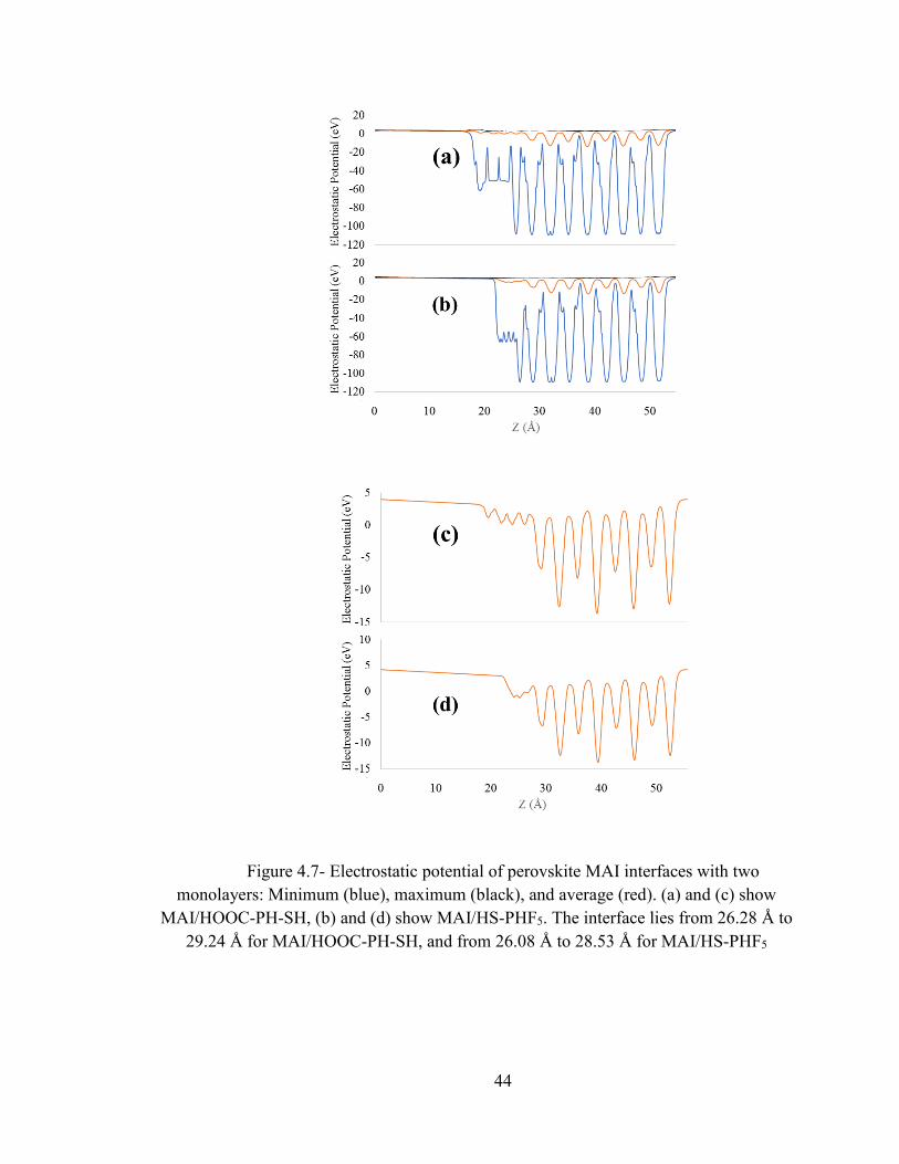
Figure 4.7- Electrostatic potential of perovskite MAI interfaces with two monolayers:
Minimum (blue), maximum (black), and average (red). (a) and (c) show MAI/HOOC-PH-

x
SH, (b) and (d) show MAI/HS-PHF5. The interface lies from 26.28 Å to 29.24 Å for
MAI/HOOC-PH-SH, and from 26.08 Å to 28.53 Å for MAI/HS-PHF5 .......................... 44
Figure 4.8- Electrostatic potential of perovskite MAI interfaces with two monolayers:
Minimum (blue), maximum (black), and average (red). A and C - PbI/HOOC-PH-SH, B
and D PbI/HS-PHF5. The interface lies from 25.22 Å to 27.66 Å for PbI/HOOC-PH-SH
and from 25.18 to 27.66 Å for PbI/HS-PHF5.................................................................... 45
Figure 4.9- Charge density plots for (a) MAI surface reconstruction and (b) PbI surface
reconstruction .................................................................................................................... 49
Figure 4.10- Zoomed-inversion of charge density plot for (a) MAI surface reconstruction
and (b) PbI surface reconstruction .................................................................................... 50
Figure 4.11- Charge density plots for MAI/HOOC-PH-SH (a), MAI/HS-PHF5 (b),
PbI/HOOC-PH-SH (c), and PbI/HS-PHF5 (d) perovskite/monolayer interfaces.............. 50
Figure 4.12- Zoomed-in charge density plots for MAI/HOOC-PH-SH (a), MAI/HS-PHF5
(b), PbI/HOOC-PH-SH (c), and PbI/HS-PHF5 (d) perovskite/monolayer interfaces ....... 51
Figure 4.13- Density of states for HOOC-PH-SH/MAI (a), HS-PHF5/MAI (b), HOOC-PH-
SH/PbI (c), and HS-PHF5/PbI (d) interfaces..................................................................... 53
Figure 4.14 Molecular dynamics snapshots with HOOC-PH-SH /MAI. (a) and (b) show
atomic positions at 500 steps and 1000 steps for 300 K, (c) and (d) show atomic positions
at 500 steps and 1000 steps for 400 K .............................................................................. 54

xi
Figure 4.15- Molecular dynamics snapshots for HOOC-PH-SH /PbI. (a) and (b) show
atomic positions at 500 steps and 1000 steps for 300 K, (c) and (d) show atomic positions
at 500 steps and 1000 steps for 400 K. ............................................................................. 55
Figure 4.16 Molecular dynamics snapshots with HS-PH-F5 /MAI. (a) and (b) show atomic
positions at 500 steps and 1000 steps for 300 K, (c) and (d) show atomic positions at 500
steps and 1000 steps for 400 K ......................................................................................... 56
Figure 4.17- Molecular dynamics snapshots with HS-PH-F5 /PbI. (a) and (b) show atomic
positions at 500 steps and 1000 steps for 300 K, (c) and (d) show atomic movements at 500
steps and 1000 steps for 400 K ......................................................................................... 57

xii
LIST OF TABLES
TITLE PAGE
Table 1 Temperature profile of phase Ccange in CH3NH3PbI3 hybrid perovskite [27] [28]
[29]. ................................................................................................................................... 27
Table 2 Total energies of optimized HOOC-PH-SH interfaces. The most stable structures
are denoted by * ................................................................................................................ 36
Table 3 Total Energy of HS-PHF5/MAI and HS-PHF5/PbI Interfaces. The lowest energy
structures are denoted by ** ............................................................................................. 38
Table 4- MAISR and PbISR average electrostatic potential ............................................ 46
Table 5- Electrostatic Potential of Interfaces .................................................................... 47
Table 6- CHARGE DENSITY THREESHOLD VALUES.............................................. 49

xiii
LIST OF ACRONYMS
CH3NH3PbI3 Methyl Ammonium Lead Halide
CsI Cesium Iodide
CBL Cathode Buffer Layer
CIGS Copper Indium Gallium Selenide
CdTe Cadmium Telluride
CZTS Copper Zinc Tin Sulfide
DFT Density Functional Theory
DSSC Dye Sensitized Solar Cell
DOS Density of states
ETM Electron Transport Material
ELF Electron Localization Function
GGA Generalized Gradient Approximation
HOOC-PH-SH 4-mercaptobenzoic acid
HS-PHF5 Pentafluorobenzenethiol
HTM Hole Transport Material

xiv
ITO Indium Tin Oxide
IBRION = 2 conjugate-gradient method
IBRION = 1 Quasi- newton algorithm
LDA Local Density Approximation
LAPW Linear argumented plane wave
MD Molecular Dynamics
MAI Methyl Ammonium Side
MAISR Surface Reconstruction in MAI side
PbI Metal Halide Side
PbISR Surface Reconstruction of PbI side
PV Photovoltaic
PAW Projector Augmented Wave Method
PCE Power Conversion Efficiency
VASP Vienna ab initio Simulation Package
VdW Vander Walls
VMD Visual Molecular Dynamics
ZnO Zinc Oxide

xv
ACKNOWLEDGMENTS
Firstly, I would like to express my sincere gratitude to my advisor Dr. Amir Farajian
for the continuous support of my master’s study and related research, for his patience,
motivation, and immense knowledge. His guidance helped me in all the time of research
and writing of this thesis. I could not have imagined having a better advisor and mentor for
my thesis.
Besides my advisor, I would like to thank the rest of my thesis committee Dr. James
Menart and Dr. Allen Jackson for their kindness and time. I would also like to thank
Siddharth Rathod, Luke Wirth and Shantanu Rachalwar for helping me in various ways
during some obstacles during the research. Also, I am thankful to Ohio Supercomputer
Center for providing needed access and resources which were essential for optimization
and without which this project would be incomplete.
Last but most importantly, to my parents for being so supportive and helping me
excel in my masters studies.

1
CHAPTER 1 INTRODUCTION
Solar Photovoltaics (PV) has attracted a lot of attention in previous 25 years.
Figure 1.1 shows an exponential growth rate in photovoltaic installed capacity in every
region. Europe leads the world in growth and installed capacity of photovoltaics. Solar
photovoltaics had an estimated global cumulative installed capacity of 110 GW by the end
of 2012 and is predicted to reach 368 GW by 2017 [1].
Figure 1.1 Installed PV capacity of different regions over the years and overall
rise in global PV capacity from 2000. [1]

2
Solar photovoltaics in simple words is defined as direct conversion process of light
(photons) into electrical energy at atomic or molecular level. The biggest property
responsible for photovoltaics is the photoelectric effect which causes materials to absorb
photons of light and generate electrons in a circuit. The electrons are responsible for electric
current in the system.
French physicist Edmund Bequerel discovered photoelectric effect in some
materials which produced electric currents on exposure to light in 1839. This was further
described by Albert Einstein in 1905 in the form of nature of light and photoelectric effect
which are the main principles on which photovoltaic applications are based [2].
1.1 BASIC OPERATION OF SOLAR CELLS
Solar cells currently are most commonly made up of semiconductor material like
silicon. The material is treated in such a way to form a p-n junction to contain an electric
field. It has alternate charge on either side positive on one end and negative on the other
end. As photon strike the solar cell, the electrons get excited to a higher energy state and
there is a flow of these high-energy electrons in the circuit. If we join conductors to this p-
n junction there will be an electrical loop formation with one positive side and one negative
side. On joining the p-n junction to electrodes the electrons with high energy are circulated
which forms electric current [2].
1.1.1 THREE GENERATIONS OF SOLAR CELLS
There are three generations in which solar photovoltaic cells are mainly classified,
as follows. First generation Solar cells: These are the conventional solar cells materials
which are made up of crystalline silicon which are single or multi.They account for about

3
80% of the current installations. Four types of silicon solar cells are present in the first
generation: 1) Monocrystalline Silicon Cells, 2) Polycrystalline Silicon Cells, 3)
Amorphous Silicon Cells, 4) Hybrid Silicon Cells. These have a considerable conversion
efficiency of 15-20%. Second generation: Thin film solar cells. This generation is classified
in three types: amorphous silicon (a-Si), cadmium-telluride (CdTe) and copper-indium-
diselenide which are not silicon and has a market share of 5%. These solar cells show 20%
conversion efficiency. Third generation of solar cells: Different materials which are non-
silicon. Some of the materials used are nanotubes, nanoparticles, organic dyes or
conductive polymers. The major goal of third generation solar cells is to have high
efficiency over a wider energy range which also includes the infrared region of light, low
cost, and environmental friendliness [2].
1.1.2 PEROVSKITE SOLAR CELLS
Perovskite solar cells are among the third-generation type of solar cells. These have
attracted a lot of attention in previous few years. These solar cells are basically made up of
hybrid organic-inorganic lead halides (ABX3). Here, A is an organic cation like methyl-
ammonium (CH3NH3+) or formamidinium (FA), B is an inorganic cations like lead, and X
is a halogen anion like chlorine, bromine, or iodine. The most famous material used is
MAPbI3. Perovskite solar cells also exists in the form of CaTiO3, BaTiO3 [4]. Perovskite
materials were known for many years but first were implemented as solar cells materials
in the year 2009 by Miyasaka et al. The first reported perovskite solar cell was dye-
sensitized with a power conversion efficiency (PCE) of just 3.8% with a very thin layer of
mesoporous TiO2 as electron collector. They have reached a PCE of 20.1 % in a span of
just 6 years (Figure 1.2). One drawback stopping it from commercialization is its less
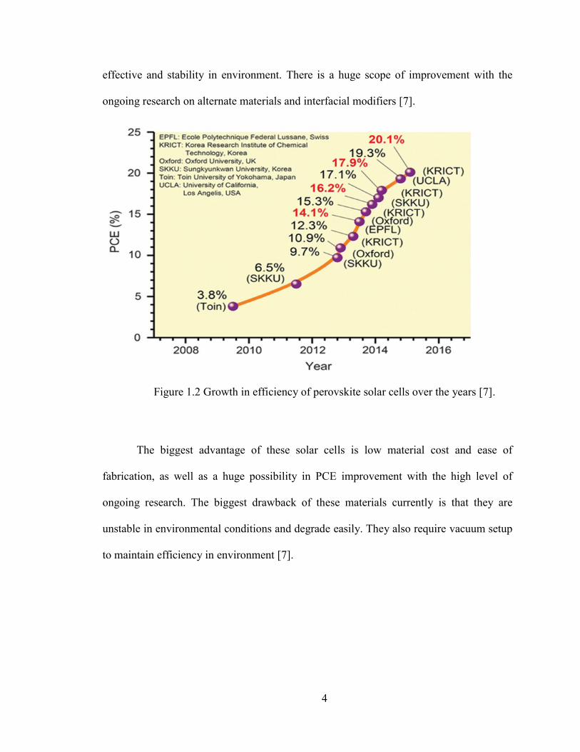
4
effective and stability in environment. There is a huge scope of improvement with the
ongoing research on alternate materials and interfacial modifiers [7].
Figure 1.2 Growth in efficiency of perovskite solar cells over the years [7].
The biggest advantage of these solar cells is low material cost and ease of
fabrication, as well as a huge possibility in PCE improvement with the high level of
ongoing research. The biggest drawback of these materials currently is that they are
unstable in environmental conditions and degrade easily. They also require vacuum setup
to maintain efficiency in environment [7].

5
CHAPTER 2 LITERATURE REVIEW
2.1 OVERVIEW
The actual perovskite solar cell setup has these major components
1) Electron transfer layer: There are two types of layers that could be used. These
are mesoporous and planer. Commonly used electron transfer layer materials are titanium
dioxide (TiO2), zinc oxide (ZnO), stannic oxide or tin oxide (SnO2), silicon dioxide (SiO2),
zirconium dioxide (ZrO2), phenyl-C61-butyric acid methyl ester (PCBM). Titanium
dioxide (TiO2) has the best properties among them and is widely used.
2) Hole transport material (HTM): Spiro-OMeTAD is the first solid state hole
transport material used with hybrid organic-inorganic perovskite-sensitized TiO2
electrodes. Currently, they are most commonly used HTM in PSC which are π-conjugated
materials.
3) Hybrid organic-inorganic perovskite components: Mostly methyl (CH3)
ammonium (NH3), metal (Pb, Sn or Eu), X3 (where X is halide group Cl, Br or I). These
components are used because the resultant band gap ranges from 1.3 to 2.9 eV, and the
band gap can also be altered by using different dopants.
(4) Counter electrode: Some of the counter electrodes used are Au and Ag [3].

6
Figure 2.1 Evolution of perovskite solar cell [7].
Figure 2.1 shows the development of perovskite solar cell design. Figure 2.1 (a) is
the first version of perovskite solar cell. It was designed in perovskite sensitized
configuration compared to the normal solar cells which were in solid state and dye
sensitized configuration. Here we see perovskite nano-dots on TiO2 surface which explains
the photocurrent generation and transfer from perovskite to TiO2 surface. Figure 2.1 (b)
shows a superstructure configuration which proves that a perovskite does not require an
electron accepting medium TiO2 or ZnO when Al2O3 is used as a supporting element. The
thin layer of perovskite is designed around Al2O3, which shows the electron transfer
properties. Figure 2.1.c shows bi-functional material feature of perovskite solar cells as it
can transport electrons and can act as both light harvesting and n-p type semiconductor.
Depending on the type of bi-functionality it could be used for complete pore filling of TiO2
film instead of spiro-OMeTAD which is normally used as hole transport medium. This

7
pore filling feature leads to capping layer formation compromising of perovskite alone, and
leading to formation of mesoscopic perovskite solar cell structure with inclusion of capping
layer. Figure 2.1 (d) shows a planar heterojunction type of arrangement as TiO2 acts as
both electron transfer and hole acceptor medium and perovskite shows optical properties
and can be applied to many solar cell configurations. Figure 2.1 (e) shows an inverted
layout which is analogous to organic photovoltaic configurations as perovskite is
sandwiched between hole collecting PEDOT:PSS layer and electron collecting PCBM
layer [7].
2.2 INTERFACIAL STUDY OF PEROVSKITE
The most common interface of Perovskite/Electron transfer material is
CH3NH3PbI3/TiO2 Interface. In this interface the CH3NH3PbI3 acts a hole transport
material and TiO2 acts as an electron transfer layer. TiO2 exists in two different structures
namely rutile and anatase. Yella et al. were the first to report that rutile TiO2 is more
efficient in extraction of electrons from the CH3NH3PbI3 layer than the anatase TiO2.
CH3NH3PbI3 can also have two types of arrangements to form an interface which are from
the methyl ammonium halide side (MAI) and metal halide side (PbI). Different power
conversion efficiencies could be achieved by having interfaces in four different
arrangements of CH3NH3PbI3 and TiO2 [5].

8
Figure 2.2 Different interfaces between CH3NH3PbI3/TiO2 [5].
Figure 2.2 represents (a) MAI/A (anatase) interface (b) PbI/A (anatase) interface
(c) MAI/R (rutile) interface (d) PbI/R (rutile) interface. The CH3NH3PbI3 used is tetragonal
and the cell lattice parameters are a (x axis) = 8.94 Å, b (y axis) = 8.94 Å and c (z axis) =
12.69 Å. CH3NH3PbI3 exists in tetragonal phase between the temperature range of 162 K
to 330 K which lies in the room temperature range and ambient condition range. There is
a phase change from tetragonal phase to cubic phase at higher temperatures and further
changes to orthorhombic phase at 162 K. In Ref. [5], for the study of interactions at the
interface they have used 7 layers (4 MAI and 3 PbI) for MAI/TiO2 interface and 4 PbI and
3 MAI for PbI/TiO2 interface with 20 Å vacuum. Electronic properties are studied.
Electron localization function (ELF), charge density difference, electrostatic potential,
partial density of states (PDOS) are studied [5].
2.2.1 ELECTRON LOCALIZATION FUNCTION (ELF)
ELF can be used to find structure flaws and form a correlation between electronic
properties of atoms and atomic structure. ELF includes the coordination of each atom by

9
identifying covalent and dangling bonds. A covalent bond is formed by overlapping atomic
orbitals, which results in an accumulation of charge between the bonded atoms. This
accumulation shows a broad maximum in the ELF along the bonding axis for non-polar
covalent semiconductors. As the bond breaks, charge is no longer localized between the
atoms, but is in atomic orbitals instead, which shows a peaks in the ELF near the atomic
positions, forming a minimum. ELF plots for four relaxed CH3NH3PbI3/TiO2 system
interfaces are shown below [5]. The numerical value of this plot is in a range from 0 to 1,
where high localization of the electrons is shown by the reddish color, and blue color
represents no localization of electrons. The green color signifies a value of 0.5 which is
electron-gas like as shown by properties of metallic nature. The difference in the structure
of the ELF along the axes between neighboring atoms can be used to distinguish whether
a bond exists or not. As the different shape also goes along with a distinctly different value
of the ELF in the center between the atoms, we can alternatively use this value as a simple
criterion for identifying a dangling bond.

10
Figure 2.3-ELF plots: (a) MAI/TiO2 (Anatise), (b) PbI/TiO2 (Anatise),
(c) MAI/TiO2 (Ruitle) and (d) PbI/ TiO2 (Rutile) [5].
2.2.2 CHARGE DENSITY DIFFERENCE AND ELECTROSTATIC POTENTIAL
The plot of charge density difference shows difference between the charge density
of hybrid perovskite interface with TiO2, compared to charge density of perovskite and
electron transfer layer.
To understand the details of charge transfer at the interface, the difference charge
densities are presented in Figure 2.4 [5], in which the blue color shows accumulation of
charges and the red color shows depletion of charges. The average of electrostatic potential
is used to describe electronic energy levels. During the time TiO2 and perovskite form an
interface, electron transfer from perovskite to TiO2 occurs because of initial Fermi energy

11
difference. This generates an electric field at the CH3NH3PbI3/TiO2 interface which is
directed from TiO2 to perovskite.
Figure 2.4 Charge Density difference plots on the left, and electrostatic potential
on the right: (a) MAI/TiO2 (Anatise), (b) Pbi/TiO2 (Anatise), (c) ) MAI/TiO2 (Ruitle), and
(d) PbI/ TiO2 (Rutile) [5].
2.2.3 ANALYSIS OF PREVIOUS INTERFACE RESULTS
We notice the following points from previous interface results [5]: 1) PbI-TiO2 surface
of CH3NH3PbI3 has a better interaction with TiO2 due to formation of bridge bond and a
better charge transfer characteristics as per ELF plot. 2) Rutile interface has a better atom

12
arrangement and lattice match with perovskite (CH3NH3PbI3) [5]. 2) For perovskite slabs,
the electrostatic potential as shown in Figure 2.3. The overall potential of TiO2 is lower
than CH3NH3PbI3, which is the drawing force towards charge transfer from Perovskite to
TiO2. The average potential difference between the two different TiO2 slabs show that
rutile structures has a better charge transfer as compared to anatise. As PbI layers have
higher potential drop it has a better electron hole separation property compared to MAI [5].
.
2.3 INTERFACIAL ENHANCERS
Interface engineering or modification is an approach towards getting stable and
efficient solar cells. This can be achieved by, e.g., focusing on electron injection properties
from MAPbI3 to electron collector medium, increasing the electron transfer and reducing
the charge recombination to minimum. Some of the interfacial enhancers and their
significant results are analyzed below.
2.3.1 4-MERCAPTOBENZOIC ACID AND PENTAFLUROBENZENETHIOL
The relevant interfaces in common hybrid perovskite solar cells are MAPbI3, TiO2
and Spiro-OMeTAD interface surfaces [6]. Research on dye sensitized solar cells (DSSC)
has shown that 4-mercaptobenzoic acid moieties could form a better connection with TiO2
surface thereby increasing electron transfer and power transfer efficiency. Based on this
research, many other interfacial modifiers were used like organic anchor HOOCRNH3+I.
3-aminopropanoic acid self-assembled monolayer (SAM) on the sol–gel ZnO layer has
shown significant improvement in performance because of the presence of alkyl chains
which are present in the binding sites. It is observed that π-electron acceptors show better
13
electron transfer characteristics [6]. In this experiment, HOOC-PH-SH is used as the
interfacial modifier for TiO2/CH3NH3PbI3 interface. The π-electron present in the thiol
group would contribute towards better power conversion efficiency. Among the main causs
of concern for commercialization of perovskite solar cells are light induced heat and
environmental moisture which causes lack of stability. To fight these problems
hydrophobic thiol-containing monolayers are used. These form a hydrophobic molecular
layer between the perovskite and the hole transfer medium (Spiro-OMeTAD). The
hydrophobic molecule which showed the best results was pentafluorobenzenethiol (HS–
C6F5). [6] The introduction of HOOC-PH-SH in CH3NH3PbI3/TiO2 interface lead to a
stable power conversion efficiency of 14.1%. Furthermore, setting up the whole assembly
with Spiro-OMeTAD / HS –C6F5/Perovskite/HOOC-PH-SH /TiO2 shows a better
environmental stability as shown below [6].

14
Figure 2.5 Environmental stability of HOOC-PH-SH/Perovskite vs. HOOC-PH-
SH/Perovskite/HS-PhF5 [6].
The entire setup is kept under environmental conditions with 45% humidity [6].
Figure 2.5 (a) shows the variation of color and degradation of two assembly. HOOC-PH-
SH/Perovskite/HS-PHF5 does not degrade in color and remains stable over a period 8 days.
On the other hand we see a drastic change in the assembly color and degradation of HOOC-
PH-SH/Perovskite assemble. Figure 2.5 (b) shows that HOOC-PH-SH/Perovskite/HS-PH-
F5 assembly is highly efficient over a period of 250 hours compared to HOOC-PH-
SH/Perovskite assembly which showed drastic drop in efficiency. Figure 2.5 (c) shows
result where the assembly is tested at AM 1.5 G illuminance [6]. HOOC-PH-
SH/Perovskite/HS-PH-F5 showed good stability compared to HOOC-PH-SH/Perovskite
15
assembly which degraded to 3% power conversion efficiency within a period of just 55
hours [6].
2.3.2 CESIUM IODIDE AS AN INTERFACIAL ENHANCER [9]
One reason of moving towards renewable energy and photovoltaic cells is it being
environmental friendly. Cesium iodide (CsI) is ecofriendly and serves as a possible way of
improving efficiency and interfacial properties of perovskite solar cells. In this setup
cesium iodide is an intermediate layer between MAPbI3 and mesoporous TiO2 (mp-TiO2).
Cesium iodide is treated in a polymer phase before being inserted between MAPbI3 and
TiO2. Results of scanning electron microscope (SEM) and atomic force microscope (AFM)
show that after introduction of cesium iodide at the interface the quality of MAPbI3 was
improved and also there was a reduced roughness with better contact in the FTO/bl-
TiO2/mp-TiO2/CsI/MAPbI3 substrate. On the energy level side, the FTO/bl-TiO2/mp-
TiO2/CsI/MAPbI3 assembly showed a shift of 0.24 eV towards the vacuum side on the
energy diagram after the cesium iodide enhancer was used in assembly. This means that
the barrier for charge injection from the perovskite to the TiO2 is reduced and also the
conduction band of the assembly better matches the conduction band of perovskite
resulting in a better electron transfer on introduction of enhancer. Optical spectroscopy
shows that the absorbance property is modified and shifts to a lower wavelength on
introduction of cesium iodide. This lower absorbance results in better performance. These
are evidences that show photovoltaic properties have improved after introduction of cesium
iodide. The power conversion efficiency (PCE) rises by 3.23% in the forward direction
scanning and 2.72% in the reverse direction scanning. The photovoltaic properties with
and without CsI are shown in Figure 2.6.

16
Figure 2.6 Photovoltaic properties with CsI and without CsI [9].
JSC and VOC have increased in forward and reverse scanning after introduction of
CsI. The reason is a decrease in work function (WF) of ETL. This resulted in increased
build in potential drop of the assembly which not only led to increase in open circuit voltage
(VOC ) but also increased the extraction of electrons thereby increasing the short circuit
current density (JSC ).

17
Figure 2.7 Environmental Stability with CsI and without CsI [9]
Figure 2.7 shows test of stability of the assembly by storing it in sampling for two
months [9]. The perovskite solar cells (PSC) without CsI interfacial enhancement showed
a very low stability. It only retained 30% of the original efficiency. The other assembly
with cesium iodide interfacial enhancement showed better environmental stability and
retained 66% of original efficiency over a period of two months [9].
18
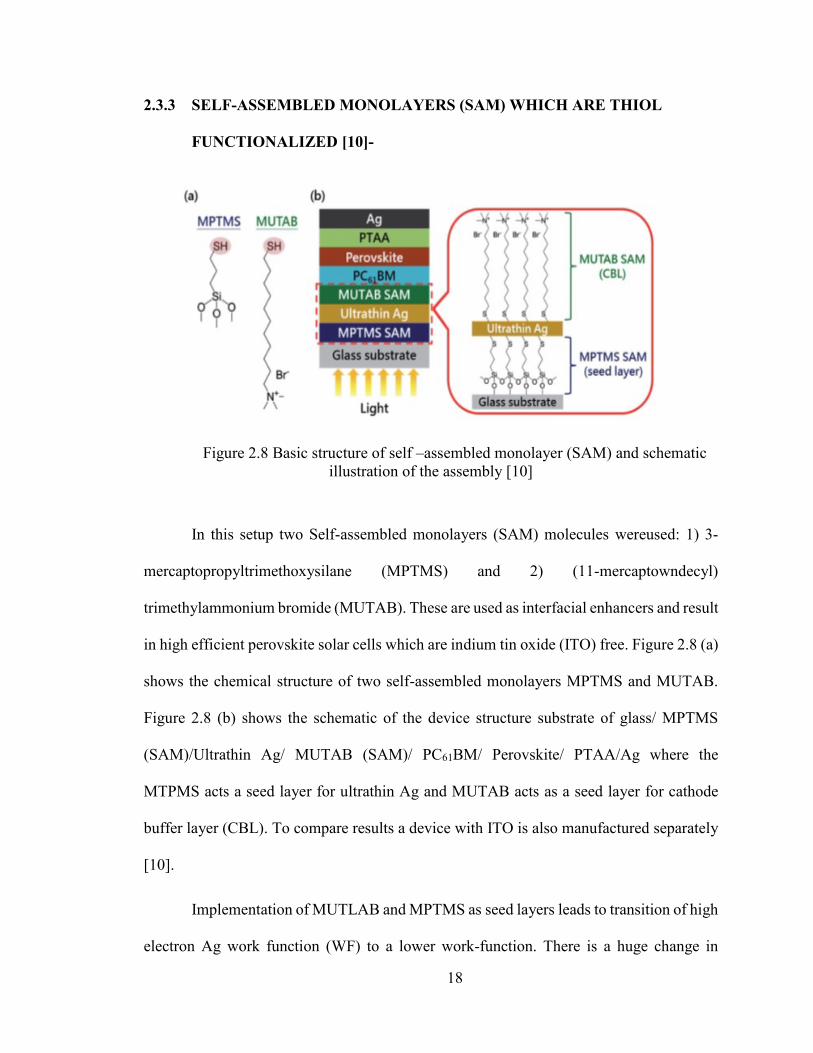
2.3.3 SELF-ASSEMBLED MONOLAYERS (SAM) WHICH ARE THIOL
FUNCTIONALIZED [10]-
Figure 2.8 Basic structure of self –assembled monolayer (SAM) and schematic
illustration of the assembly [10]
In this setup two Self-assembled monolayers (SAM) molecules wereused: 1) 3-
mercaptopropyltrimethoxysilane (MPTMS) and 2) (11-mercaptowndecyl)
trimethylammonium bromide (MUTAB). These are used as interfacial enhancers and result
in high efficient perovskite solar cells which are indium tin oxide (ITO) free. Figure 2.8 (a)
shows the chemical structure of two self-assembled monolayers MPTMS and MUTAB.
Figure 2.8 (b) shows the schematic of the device structure substrate of glass/ MPTMS
(SAM)/Ultrathin Ag/ MUTAB (SAM)/ PC61BM/ Perovskite/ PTAA/Ag where the
MTPMS acts a seed layer for ultrathin Ag and MUTAB acts as a seed layer for cathode
buffer layer (CBL). To compare results a device with ITO is also manufactured separately
[10].
Implementation of MUTLAB and MPTMS as seed layers leads to transition of high
electron Ag work function (WF) to a lower work-function. There is a huge change in

19
interfacial properties. The power conversion efficiency (PCE) for areas of 0.12 cm2, 1.2
cm2, and 5.04 cm2 are 16.2 %, 15.98%, and 12.79% respectively, compared to 13.4%
showed by ITO devices [10].
The environmental stability was also tested by keeping in external environment for
over 1000 hours. The results showed it retained 65% of the initial PCE after 1000 hours
which is way more effective than MAPbI3 and FAPbI3. Some other good properties noted
by AFM analysis is better surface contact and smooth surface with average transmittance
of 78% [10].
20
CHAPTER 3 THEORY
This chapter gives a theoretical overview and introduces the simulation software
Vienna Ab Initio Simulation Package (VASP) which is used to perform structural
optimizations and electronic properties calculations for the thesis. We compute the
structural configuration, system properties like total energy and interactions between atoms
using first principles, utilizing density functional theory (DFT) implemented in VASP
code. We explain an overview of DFT and the exchange correlations approximations we
considered for calculations and the inputs and outputs in VASP for system optimization.
Chapter 3 is a continuation of chapter 2 and describes the methodology implemented for
optimization of CH3NH3PbI3 and Carboxylic acid thiol and the CH3NH3PbI3/COOH-Ph-
SH interface and CH3NH3PbI3/HS-PH-F5 interface. The process of interface formation and
finding the location of the two monolayers at the interface with desired settings in VASP
are explained.
3.1 DENSITY FUNCTION THEORY (DFT)-
Density function theory (DFT) is one of the methods used for computational
quantum mechanical modelling of materials which include metals, insulators and
semiconductors. It has a prime aim of achieving ground state electronic properties of atoms
or molecules by numerically solving Schrödinger equation. DFT started to get popular in
1970’s especially for the calculations related to solid state physics. However it was in 1990s
when it started getting popular for quantum chemistry when many approximations were

21
introduced and there were many available good exchange correlation interactions. In 1998
Walter Kohn one of its founders got a Noble Prize in Chemistry. Accuracy and significantly
lower cost for computing data are the reasons why DFT is better than Hartree-Fock method.
The second reason is that Hartree Fock method does not apply to metals. Even with the
current developments of DFT, it still lags in accuracy to define intermolecular interactions
specifically for van der Waals forces, the excitations involved in charge transfer, the
transition from one state to another state, and interactions while inserting dopants for
interfacial study. It also lags accuracy in calculations of some properties of semiconductors
which include band gap and ferromagnetism.
3.1.1 SCHRÖDINGER EQUATION
The Schrödinger equation is the basic starting concept for DFT study. The
Schrödinger equation exists in two forms 1) Time dependent Schrödinger equation and 2)
Time independent Schrödinger equation. Time-independent Schrödinger equation is given
in equation 3.1.1 [ 8].
Ĥ𝛹 = 𝐸𝛹 (3.1.1)
In the equation 3.1.1 Ĥ represents the Hamiltonian operator which is interpreted to
be equal to the total energy, Ψ is the wave function which is in stationary state, E is the
eigenvalue energy which is the energy of the stationary state Ψ [8]. Equation 3.1.2 shows
an elaborated version of equation 3.1.1 where the Hamiltonian has two parts; one kinetic
part and potential part and is separated by the separation of variables method.
[(−ℏ2
2𝑚) d2 𝛹/dx2 + 𝑉Ψ] = 𝐸Ψ (3.1.2)

22
This Schrödinger equation for a single particle which is under the external influence
of nuclei potential V. m represents the particle mass and h is the Planck’s constant. Single
particle theory holds a little value for the study of materials including numerous atoms. To
solve this problem, equation 3.1.2 is modified to account for many particles [8].
3.1.2 EXCHANGE CORRELATION APPROXIMATIONS
System properties depend on total system energy, including the exchange-
correlation energy. This is included in the Kohn-Sham equations that is used in many-
particle calculations by mapping an interacting system onto a non-interacting auxiliary
system. The kinetic energy which is related to Kohn-Sham equations is not a true form of
kinetic energy and this could be used to define an exchange energy functional. Exchange-
correlation energy is a form of energy that corresponds to exchange in positions with same
spin criteria between two or more electrons. We can use Equation 3.1.2.1 for the exchange-
correlation energy [11] [12]
𝐸𝑥𝑐[(𝑛𝑟)] = 𝑇[(𝑛𝑟)] + 𝑇𝑠[(𝑛𝑟)] + 𝐸𝑒𝑒[(𝑛𝑟)] + 𝐸𝐻[(𝑛𝑟)] (3.1.2.1)
In Equation 3.1.2.1 𝑇𝑠[(𝑛𝑟)] represents the true kinetic energy, 𝐸𝑒𝑒[(𝑛𝑟)]
represents the interactions between electrons. The term 𝐸𝑥𝑐[(𝑛𝑟)] in the above equation is
described by introducing an approximate functional. There are two most commonly used
approximations: Local Density Approximation (LDA) that is a functional which is
generally based on local density [11], and Generalized Gradient Approximation (GGA)
that is a functional which is based on local energy and its gradient [12]. The simplest form
of approximation is LDA. In this approximation there is an assumption that the exchange-
correlation functional at any given position r must be equal to the exchange-correlation

23
functional energy of a free electron gas possessing similar density at that given point r.
Exchange-correlation energy (𝐸𝑥𝑐𝐿𝐷𝐴 ) is represented by equation 3.1.2.2. The exchange
correlation potential (𝑣𝑥𝑐𝐿𝐷𝐴) is represented by equation 3.1.2.3
𝐸𝑥𝑐𝐿𝐷𝐴[𝑛(𝑟)] = ∫ 𝜀𝑥𝑐(𝑟)𝑛(𝑟)𝑑𝑟, (3.1.2.2)
𝑣𝑥𝑐𝐿𝐷𝐴[(𝑟)] =
𝛿𝐸𝑥𝑐𝐿𝐷𝐴[𝑛(𝑟)]
𝛿𝑛(𝑟)=
𝜕 [𝑛(𝑟) 𝑥𝑐(𝑟)]
𝜕𝑛(𝑟) (3.1.2.3)
𝜀𝑥𝑐(𝑟) = 𝜀𝑥𝑐ℎ𝑜𝑚[𝑛(𝑟)] (3.1.2.4)
The full representation of 𝜀𝑥𝑐(𝑟) in the exchange-correlation potential is shown in
equation 3.1.2.4 where 𝜀𝑥𝑐ℎ𝑜𝑚 is derived, e.g., by Quantum Monte Carlo (QMC) [13] [14]
calculations which are based on similar electron gases tested at different densities. These
parameters are used for interpolation formulations to get all the results.
One drawback in LDA is that no correction to the exchange-correlation energy is
available that is related to non-uniformity in the densities of electrons at position r.[15]
LDA is considered effective despite drawbacks. Its over-binding nature especially in case
of molecules leads to utilization GGA instead. [15]
GGA uses a semi-local methodology and includes the effects of non-uniformity by
introduction of electron density gradient. The GGA exchange potential is shown in
equation 2.1.7
𝐸𝑋𝐶𝐺𝐺𝐴[𝑛(𝑟) = ∫ 𝑛(𝑟)𝜀𝑥𝑐
ℎ𝑜𝑚[𝑛(𝑟)]𝐹𝑥𝑐[𝑛(𝑟), ∇𝑛(𝑟)]𝑑𝑟 (3.1.2.5)
In the equation 3.1.2.5 𝐹𝑥𝑐[𝑛(𝑟), ∇𝑛(𝑟)] represents an improvement factor. There
are many available improvement factors. [12][16][17][18]. GGA shows better results when
24
applied to a system of molecules and also reduces the effect of over-binding of molecules
that happened in LDA. This makes GGA a more effective exchange correlation.
3.2 MOLECULAR DYNAMICS
In this research, ab initio molecular dynamics is performed by using VASP
software. Molecular dynamics is the study of movement of atoms at atomic scale. The
atoms are allowed to move at very small time-steps on the order of femtoseconds. The
results are analyzed using a visualizing software like Visual Molecular Dynamics (VMD).
VASP finds out the forces by using some approximations which depend on the
potential energy acting on each atom. To consider the energy contributions of electrons in
the total energy, we use density function theory. To consider the forces affecting the atoms
VASP uses periodicity which means that a single unit cell is replicated periodically. VASP
uses plane-wave basic sets for solving total energy equations.
3.3 Viena Ab-initio Simulation Package (VASP)
VASP is the software used for structural optimization and electronic properties
analysis in our thesis. VASP is an ab initio simulation software which is used to model
materials at atomic scale. VASP determines the electronic ground state of molecules by
using iterative matrix diagonalization. The interactions between different electrons and
different ions in the system are estimated by using norm-conserving pseudo-potential
technique and projector-augmented wave method (PAW) method. We use the PAW
method for calculations in our thesis. A description is given below. We also explain the
input parameters in VASP [21-24].

25
3.3.1 Technique used for Electronic Structure Calculation
Projector Augmented Wave Method (PAW) is a method used for ab initio
calculations, in particular system’s electronic structure in solids. It was first introduced by
Blöch [19]. It is a concept which is obtained from inference of pseudopotential method
and linear augmented plane wave (LAPW) method. PAW method includes a big advantage
of the pseudopotential method by retaining the theoretical background and also keeping
the physics related to the calculations of all electrons. This includes the right nodal behavior
of wave functions of all valence electrons. It also exhibits a good ability of showing the
states of upper core electrons in addition to the valance shell electrons which are not present
in Pseudopotential method [20].
3.4 VASP Calculation Settings
The simulations of this thesis are performed using VASPbased on the following
settings: Plane-wave cutoff: 400 eV, maximum forces on atoms after optimization: 0.01
eV/Å, inclusion of van der Waals interactions, k-space mesh: 3×3×1, and molecular
dynamics time-step: 0.5 femtoseconds.
26
CHAPTER 4 RESULTS AND DISCUSSIONS
In this chapter, we discuss our results on optimization and electronic structure of
CH3NH3PbI3 hybrid perovskite interface with two monolayers HOOC-PH-SH and HS-
PHF5 for interfacial properties study. We start with the bulk perovskite optimization
followed by surface reconstruction in the perovskite. We also optimize the two molecules
to be used for monolayer construction separately. The surface reconstructed perovskite,
and the optimized molecules are used for formation of interfaces. We assume that each
monolayer can forms six initial interfaces with perovskite. Three interfaces with 1) MAI
side of Perovskite and three interfaces with 2) PbI side of perovskite. We get a total of 12
optimized interfaces after relaxation of the structures. We find out the best interfacial fit
by the lowest energy on each side with each molecule to get four most stable structures.
These four structures are then used to find the interfacial electronic properties: We calculate
charge density, electrostatic potential, and density of states to find how these molecules
affect the charge transfer properties and the photovoltaic properties of the CH3NH3PbI3
interface.
4.1 Unit Cell Tetragonal CH3NH3PbI3 and Surface Reconstruction
We start the optimization by using single perovskite in tetragonal phase. We choose
the tetragonal phase because we want to analyze the perovskite at room temperature.
CH3NH3PbI3 is in orthorhombic phase at all temperatures which are below 161 K, there is
a phase change above 161 K, and it converts to a tetragonal phase which lasts till 330 K,
27
above 330 K hybrid perovskite has a cubic phase. As the normal room temperature is
around 300 K, we select tetragonal phase for our calculations. The phase change profile is
shown in Table 1 below. [27][28][29].
Perovskite Orthorhombic Tetragonal Cubic
Temperature range <161 161 K to 330 K >330 K
Table 1 Temperature profile of phase Ccange in CH3NH3PbI3 hybrid perovskite
[27] [28] [29].
We took the initial coordinates from the reported data [30], and chose the
coordinates at 293 K corresponding to tetragonal phase. We also needed van der Walls
(vsW) function because in our system we have interaction between atoms with no chemical
bond between them. Such interactions occur between the organic element of perovskite
and inorganic element, and lead to the necessity of including vdW forces to hold these
atoms at the minimum energy positions within the unit cell.
The tetragonal phase of CH3NH3PbI3 has 48 atom and four layers, out of which two
are MAI layers, and the other two are PbI layers. The cell volume of optimized
CH3NH3PbI3 was 987.84 Å3 which matched the initial input volume after optimization. We
use the optimized unit cell for the construction of the 2-unit cell slab structures for surface
reconstruction on PbI side and MAI sides.
After this step, we form a two-unit-cell slab out of the single unit cell optimized
structure to build a 96 atom structure. We now have four layers of PbI and four layers of
MAI. Figure 4.1 shows the final structure for surface reconstruction in two different views.
28
The surface reconstruction was achieved by selectively optimizing the two-unit-cell slab:
by fixing one of the unit cells while letting the other one relax. For optimizing the surface
reconstruction in MAI and PbI sides we allow layers 1 to 4 of bulk perovskite move, while
layers 5 to 8 are kept fixed as shown in Figure 4.1 and Figure 4.2. In these structures, we
have a length of 24.24 Å for the two perovskite unit cells, and allow a vacuum of 20 Å, so
a total approximate of 45 Å was decided as the unit cell size.
Figure 4.1 represents the optimized reconstructed PbI side of perovskite. When
we compare the moving layers 1 to 4 in figure 4.1, we especially see displacement in the
first layer where we find a slight change in orientation of iodine atoms going below the
unit cells by 0.48 Å to 0.89 Å along the Z-axis of the four iodine atoms in the layer 1. If
we see layer 2 which is the MAI layer we observe slight movement of about 0.05 Å of the
iodine atoms away from the lead atoms while the carbon atoms move towards the lead
atoms by 0.1 Å. We observe a slight movement in the layer 2 as the iodine atom of layer 2
goes a bit closer to carbon of layer 2.

29
Figure 4.1- (a) and (c) show two views of optimized bulk unit cells of hybrid
perovskite with 90° rotation in horizontal plane between them, and (b) and (d) show two
views of optimized surface reconstruction on PbI side
If we see 3rd layer and compare it with 5th layer which is fixed, we see an increase
in the distance between layers. The iodine atoms have moved away by 0.45 Å along Z
direction while the lead atoms have moved by 0.36 Å along Z direction, which shows the
movement of the layer towards layers 1 and 2. There is no significant movement and no
observable surface modification in 4th layer which looks like the original surface. Figure
4.2 shows surface reconstruction for MAI side. In Figure 4.2 we fix layer 5 to 8 when layer
1 to 4 are allowed to relax during optimization. We see little reorientation taking place in

30
the 1st layer, where the iodine atom moves slightly towards the adjacent unit cell and we
also see the iodide atoms moving a bit down in the Z axis. The carbon-nitrogen bonds have
rotated by around 60° in the unit cell.
Figure 4.2 (a) and (c) show two views of optimized bulk unit cells of hybrid
perovskite with 90° rotation in horizontal plane between them, and (b) and (d) show two
views of optimized surface reconstruction on MAI side
On comparing 2nd layer we see the lead atoms moving away from the nitrogen
atoms and the iodine atoms from 1st layer. The iodide atoms of 2nd layer show a different
but larger movement compared to lead atoms. It is observed that the surface is not
destructed but only slightly moves away from 1st layer. On comparing 3rd layer we see

31
slight movement of iodine atoms towards the left unit cell and a slight movement of the
carbon and nitrogen bonded atom towards the right. The iodine atoms move slightly away
from the 2nd layer. On comparing 4th layer, we do not see any surface reconstruction where
the atoms have almost the same positions as in bulk. There is a small change which is slight
movement away from fixed layer 5 and towards the moving layer 3.
4.2 OPTIMIZATIONS OF MOLECULES FOR MONOLAYERS
Figure 4.3- Figure (a) shows 4-mercaptobenzoic acid (b) shows pentafluorobenzenethiol
4.2.1 HOOC-PH-SH
We prepared the initial input structure for the 4-mercaptobenzoic molecules by
using the GaussView software. HOOC-PH-SH is a 16 atom molecule. The reason why we
chose this monolayer for our work is that we wanted to computationally check the
experimentally reported results which showed that COOH-PH-SH would enhance the
power conversion efficiency when tested along with HOOC-[CH2]2-SH, HOOC-[CH2]6-
SH during interface formation between CH3NH3PbI3 and TiO2.

32
We used the initial GaussView structure and optimized it using VASP with
Gamma-point (k=0) in reciprocal space because it is not a periodic structure. Other than
this difference, we used the same settings as used in the perovskite optimization. The
optimized structure of this molecule (Figure 4.3 (a)) was planer.
4.2.2 HS-PhF5 (Hydrophobic Thiolates)-
We prepared the initial structure of HS-PHF5 in Gauss View. HS-PHF5 is a 13 atom
molecule. We chose this monolayer for our stimulation work is because this molecule is
hydrophobic in nature. One obstacle for practical implementation of perovskites is its lack
of stability under environmental conditions. When HS-PHF5 is in interface between
perovskite and Spiro-OMeTAD it leads to formation of a hydrophobic layer which reduces
water intercalation and results in less destruction of surface and longer life. HS-PHF5
proved to have the best results when experimentally tested against HS-PhF, HS-PhF2, HS-
PHF3, HS-C4H9 [6].
We optimized the initial structure by using VASP with just a minor change in the
settings compared to perovskite optimization that is by using only Gamma points because
the molecule is non-periodic [6]. The optimized molecule is shown in Figure 4.3 (b).
4.3 INTERFACE FORMATION USING MONOLAYERS -
Our aim was to consider formation of interfaces with two monolayers for study on
interfacial properties. We formed 12 interfaces in total out of which 6 interfaces were for
the PbI side of perovskite while 6 interfaces were for MAI side of perovskite. The 6

33
interfaces on each side consisted of 3 interfaces for each of the two molecules based on 3
different locations.
4.3.1 Interface with the PbI Side of Perovskite –
We used the optimized results from the surface reconstruction of PbI side as
explained before in this Chapter. We initially set the monolayer as straight as possible
below the PbI side of reconstructed perovskite surface. As there was no specific location
mentioned in the experimental results, we put the monolayers at 3 different locations by
using GaussView. These 3 locations for PbI side are 1) Center Pb 2) Iodine 3) Hollow. We
formed the first interface by moving the molecules towards the center of perovskite and
below the lead atom. We kept the monolayer strait and gave a distance of around 2.7 Å to
2.75 Å between sulfur and lead by using the nominal bond length from GaussView
structure construction, which was 2.55 and gave an extra 1.5 Å to 2 Å distance to allow
room for unbiased optimization. We also checked that the GaussView S-Pb bond length
approximately matches the value in published results [31].
We used the initial structure of the first guess to form the structure for third which
was the hollow position. In this position, we had an aim of moving the molecules to the
location in between iodine and lead. We brought the molecule in the vicinity of bond
lengths of respective inter-atomic bonds. We brought the sulfur of the molecule to a
distance of 2.7 Å from lead atom and 2.6 Å from iodine atom for the HOOC-PH-SH
monolayer interface while we could get near 2.8 Å from lead atom and 2.65 Å from the
iodide atom for HS-PhF5 monolayer. The nominal bond length between sulfur and iodine
is 2.34 Å. We also checked that the bond length given by GaussView reasonably matched
the ones from published sources [31] [32] [33].

34
We used the third position guess for getting the second guess structure, that is under
iodine. We brought the molecule to the left or right side of the iodine position and set it
close at the S-I nominal bond length but gave a small space to allow unbiased optimization.
We kept a distance between sulfur and iodine to about 2.55 Å to 2.6 Å for both of the
monolayers. This initial bond length from GaussView approximately matches the reported
results [32] [33].
4.3.2 Interface with the MAI side of Perovskite-
We use the same procedure but there would be slight changes with the input initial
positions of molecules at the interface. We used the optimized results from the surface
reconstruction of MAI Side which was explained before in this Chapter. We followed a
procedure similar to the one explained for the PbI side, but put the molecule at these 3
different locations: 1) Carbon Side (denoted by CS), 2) Hollow Side- It is between carbon,
iodine and nitrogen 3) Iodide side (denoted as most central).
4.4 Effect of Optimization on the Interfaces of CH3NH3PbI3 MAI and
PbI with HOOC-PH-SH Monolayer-
After setting the initial structures of interface between hybrid perovskite MAI and
PbI surfaces and the HOOC-PH-SH monolayer as explained in previous sections, we
optimize the structure using selective dynamics. This fixes one unit cell of perovskite away
from the interface and allows the rest of the structure to relax. The settings were the ones
explained in Chapter 3. The optimized structures are depicted in Figure 4.3, and the energy
35
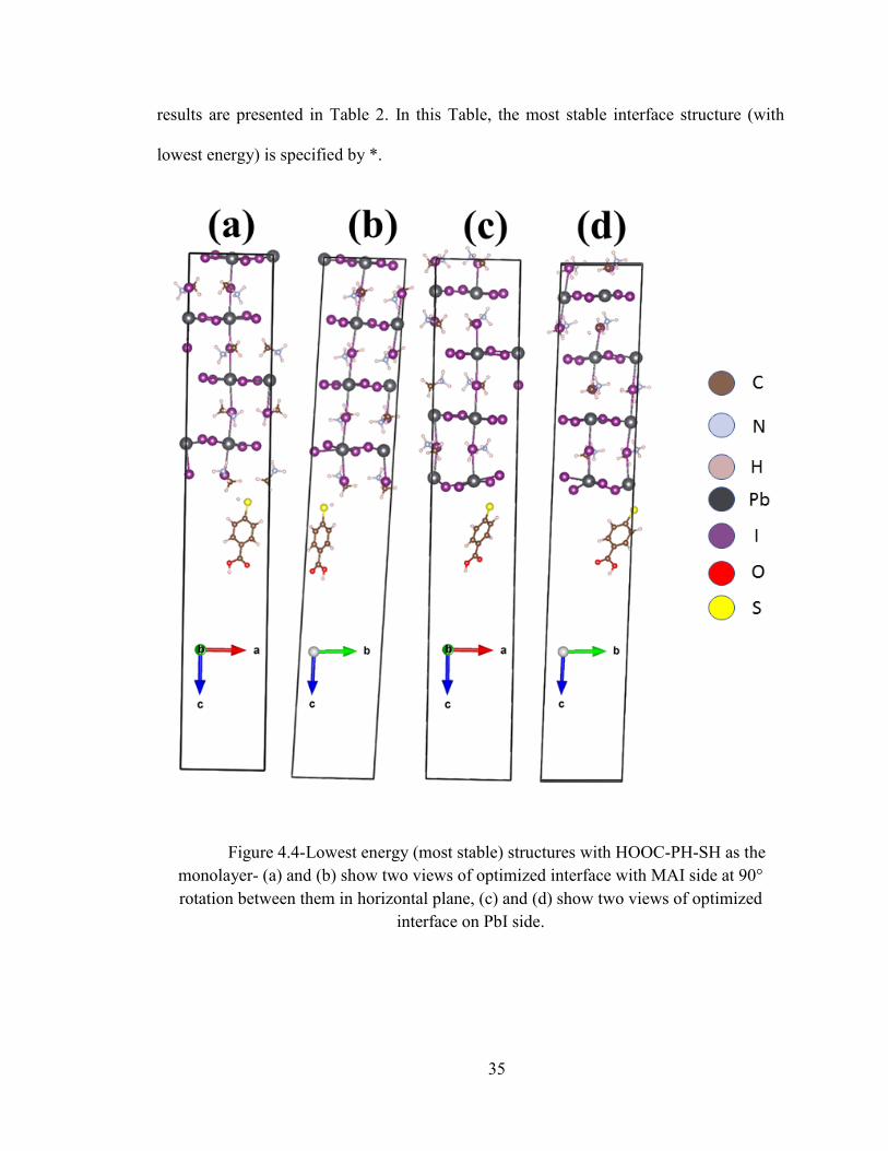
results are presented in Table 2. In this Table, the most stable interface structure (with
lowest energy) is specified by *.
Figure 4.4-Lowest energy (most stable) structures with HOOC-PH-SH as the
monolayer- (a) and (b) show two views of optimized interface with MAI side at 90°
rotation between them in horizontal plane, (c) and (d) show two views of optimized
interface on PbI side.

36
Table 2 Total energies of optimized HOOC-PH-SH interfaces. The most stable
structures are denoted by *
4.4.1 MAI/HOOC-PH-SH interface
According to Table 2, the carbon side for initial monolayer position provides the most
stable after optimization on MAI surface. Figure 4.3 (a) and (b) show the result of this
optimization. The structural characteristics of this most stable structure are as follows. By
comparing initial structure with final one, we see that the surface is not distorted and there
is no significant reconstruction in perovskite. Visually we can see one difference which is
movement of the monolayer from the initial location. The initial location of monolayer was
formed with C-S having a distance of 1.95 Å but after optimization we see that it elongated,
having a distance of 3.81 Å. The molecule has changed its orientation angularly too and
looks straighter as compared to the initial setting. The angular change is from 123° between
the S-C-C to 117° between S-C-C. When we compare the Z coordinates we see the S atom
moving down by 0.58 Å as compared to initial setting. We also see small movement in the
perovskite layers where there is small rearrangement. The first and the third MAI layers
show the movement of nitrogen and carbon atoms which are 0.121 Å in the first layer and
0.1 Å in the third layer along the Z axis. If we check layers 2 and 4 which are PbI layers
we see that one of the lead atoms in layer 2 has moved away from fixed layers by 0.1 Å
Interface type Interface Type
HOOC-Ph-SH/MAI Total Energy (eV) HOOC-Ph-SH/PbI Total Energy (eV)
Carbon Side * 0.000 Center Pb * 0.000
Hollow Side 5.338 Hollow Side 0.059
Iodine Side 5.228 Iodine Side 0.013

37
while the others have moved by a very small distance. The layer 1 and layer 3 are the MAI
layers and have 2 iodine each. We see one iodine atom in layer 1 move by 0.15 Å away
from fixed layers along the Z axis while the other iodine atom does not move significantly.
In layer 3 we see that one iodine atom move by 0.12 Å while the other atom does not move
significantly. Layer 2 and 4 have 4 iodine atoms and we have 2 atoms in each layer which
move along Z axis by 0.16 Å.
4.4.2 PbI/HOOC-PH-SH interface
According to Table 2, the initial position Center PbI results in the minimum energy and
hence the most stable structure for the PbI/HOOC-PH-SH interface. Figure 4.3 (c) and (d)
show this interface after optimization. The structural characteristics of this most stable
PbI/HOOC-PH-SH interface are as follows. By comparing the initial structure with the
final one we can visually see reorientation at the interfaces. The iodide atoms in the 1st
layer have clear movement while other atoms do not seem to have much movement. We
see that the monolayer has a small tilt and seems to move away from the interface which
is verified by its distance from lead which was 2.7Å in the initial configuration and has
changed to 3.24 Å. We also see the monolayer moving away from the surface by 0.192 Å
along the Z axis. We check for rearrangement of perovskite layers also by checking
movements along the Z axis. Carbon and nitrogen atom movements are seen in 2nd and 4th
layers. We observe that 2nd and 4th layers have an average carbon atom movement of 0.15
Å towards the upper adjacent layer. For the nitrogen atoms in the 2nd layer only one atom
moves towards the adjacent layer by 0.43Å, while both the atoms in 4th layer move by an
average of 0.2Å towards the upper adjacent layers. Only one out of two lead atoms has

38
movements of 0.189Å and 0.151Å in the 1st and 3rd layers. Iodine atoms at the interface of
1st layer show the highest movement towards the 2nd layer. The average movements of
iodine atoms in 1st layer is 0.24Å and in 3rd layer is 0.15Å. By observing the movements
we see that PbI/HOOC-PH-SH interface structure has relatively small movement of the
monolayer and the interface seems more stable than the MAI/HOOC-PH-SH interface.
This is also confirmed by the lower energy of PbI/HOOC-PH-SH interface, as presented
in Table 2.
4.5 Effect of Optimization on CH3NH3PbI3 (MAI)/HS-PH-F5 and
CH3NH3PbI3 (PbI)/HS-PH-F5 interfaces –
Table 3 Total Energy of HS-PHF5/MAI and HS-PHF5/PbI Interfaces. The lowest
energy structures are denoted by **
Interface type Interface Type
HS-PhF5/MAI Total Energy (eV) HS-PhF5/PbI Total Energy (eV)
Carbon Side 4.251 Center Pb 0.059
Hollow Side 0.089 Hollow Side 0.093
Iodine Side * 0.000 Iodine Side * 0.000

39
Figure 4.5-– Lowest energy (most stable) structures with HS-PhF5 as the
monolayer. (a) and (b) show two views of optimized interface with MAI side with 90°
rotation between them in horizontal plane, (c) and (d) show two views of optimized
interface on PbI side

40
Similar to the case of interfaces with HOOC-PH-SH monolayer, we use the settings
explained in Chapter 2 to optimize the initial structures for the HS-PHF5 interfaces. The
resulting most stable structures are depicted in Figure 4.4, and the corresponding energies
are presented in Table 3.
4.5.1 MAI/HS-PHF5 Interface-
According to Table 3, the Iodine initial site results in the most stable MAI/HS-PHF5
interface structure upon optimization. Figure 4.4 (a) and (b) show two views of this
optimized structure. Structural characteristics are as follows. By comparing the initial
interface coordinates of the Iodide side with the final optimized coordinates, we do not see
much of the reorientation in the perovskite side but there is a noticeable orientation change
of the monolayer. We can see a clear angular twist of the monolayer and moving away
from the perovskite surface, which is shown by the sulfur atom moving away by 1.56Å
along Z axis. We initially started with the sulfur atom and iodine having a distance of 2.6
Å before optimization and it changed to be 4.55Å after optimization.
If we check the atomic effect on moving layers of perovskite we see that one carbon
in 1st layer and one nitrogen in 3rd layer have movement and reorientation. We see the
carbon move away from surface by 0.108 Å while the nitrogen move towards the fixed
layers by 0.105 Å. We do not see any significant movement in lead and iodine, as well as
other carbon and nitrogen atoms, which shows the stability of this interface. This is also
manifested in Table 3 where the MAI/HS-PHF5 interface structure optimized from the
iodine initial site has the lowest overall energy.

41
4.5.2 PbI/HS-PHF5 Interface-
According to Table 3, the structure optimized from the initial iodine site has the
lowest energy, and is therefore the most stable PbI/HS-PHF5 interface structures. This
structure is shown in Figure 4.4 (c) and (d). Structural characteristics are as follows. By
comparing the initial and final structures we can clearly see reorientation in the 1st PbI layer
where the iodine shows large movement while the other layers seem to be stable. The
stability of the monolayer in this structure is high because there is no angular twist
compared with the initial orientation. Due to the interactions we see the iodine atom
moving away from the interfacial surface. The I-S bond length started with 2.8 Å and after
optimization changed to 3.7Å.
We checked all the movements along the Z direction from layers 1 to 4 of
perovskite. Carbon movements are similar in 2nd and 4th layer and we see an average
movement of 0.13 Å which is towards the fixed layers. For nitrogens in the 2nd layer, one
nitrogen atom moves by 0.33 Å towards the fixed surface while the other nitrogen atom
moves away towards the moving layer by 0.33 Å. Nitrogen atoms in 4th layer move towards
the fixed layers by an average of 0.25 Å. Lead atoms have a similar movement in 1st and
3rd layer where only one atom has movement of 0.14 Å in both layers while the other atoms
has very marginal movement. Iodine atoms has highest movement overall in the 1st layer
where we see an average movement of 0.31 Å as one atom moves significantly, while in
the 3rd layer we see a movement of 0.2 Å.

42
4.6 ELECTROSTATIC POTENTIAL-
We use the electrostatic potential curves to study the electronic properties of the
interface related to charge separation and transport. We check the effects of the interfacial
modifications caused by monolayers on the Hole Transport Medium and Electron Transfer
Medium. The results of our simulations are compared with the experimental results.
Figure 4.5 and 4.6 and 4.7 show the electronic potential of individual perovskites surface
reconstruction and for MAI and PbI side interfaces for both of the monolayers. For the
MAI side the interface is between sulfur and MAI layer. We take the average of carbon,
nitrogen and iodide atoms to decide the average distance of perovskite part of interface
along Z axis. We take the Z coordinate of sulfur as the average starting point for the
monolayer part of interface. For PbI side the interface is between sulfur location of
monolayer and the PbI layer. We take the average of lead and iodine Z coordinates for
the average position of the perovskite part of interface. The interface lies from 26.28 Å
to 29.24 Å for MAI/ HOOC-PH-SH, from 26.08 Å to 28.53 Å for MAI/HS-PHF5, from
25.22 Å to 27.66 Å for PbI/HOOC-PH-SH, and from 25.18 to 27.66 Å for HS-PHF5/PbI,
where all distances are along Z axes. In Fig 4.5, 4.6 and 4.7, (a) and (b) consist of
minimum, average and maximum potential, (c) and (d) consists of only average
electrostatic potential.

43
Figure 4.6- Electrostatic potential of perovskite surface reconstructions (SR):
Minimum (blue), maximum (black), and average (red). (a) and (c) show MAISR, (b) and
(d) show PbISR
44
Figure 4.7- Electrostatic potential of perovskite MAI interfaces with two
monolayers: Minimum (blue), maximum (black), and average (red). (a) and (c) show
MAI/HOOC-PH-SH, (b) and (d) show MAI/HS-PHF5. The interface lies from 26.28 Å to
29.24 Å for MAI/HOOC-PH-SH, and from 26.08 Å to 28.53 Å for MAI/HS-PHF5

45
Figure 4.8- Electrostatic potential of perovskite MAI interfaces with two
monolayers: Minimum (blue), maximum (black), and average (red). A and C -
PbI/HOOC-PH-SH, B and D PbI/HS-PHF5. The interface lies from 25.22 Å to 27.66 Å
for PbI/HOOC-PH-SH and from 25.18 to 27.66 Å for PbI/HS-PHF5
46
Table 4- MAISR and PbISR average electrostatic potential
Perovskite reconstruction
type
MAISR PBISR
Average Potential (eV) -2.83 -2.70
Using Figures 4.5, 4.6, and 4.7, we consider the average potential electrostatic
potential for comparisons. These are given in Tables 4 and 5. Comparing the electrostatic
potentials for reconstructed perovskite surfaces without monolayers presented in Figure
4.5 and Table 4, with those of the surfaces with monolayers (i.e. interfaces) presented in
Figures 4.6 and 4.7 and Table 5, we notice that adsorption of monolayers changes the
electrostatic potential of the perovskite. This is because structural changes caused by
monolayers. For interfaces, the individual system potential drops are calculated as the
difference between average monolayer potential and average perovskite potential. We see
that both of the monolayers are at a higher potential than that of the perovskite (Figures 4.6
and 4.7).
47
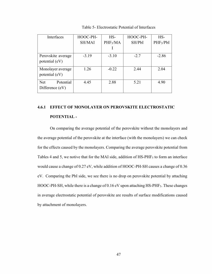
Table 5- Electrostatic Potential of Interfaces
Interfaces HOOC-PH-
SH/MAI
HS-
PHF5/MA
I
HOOC-PH-
SH/PbI
HS-
PHF5/PbI
Perovskite average
potential (eV)
-3.19 -3.10 -2.7 -2.86
Monolayer average
potential (eV)
1.26 -0.22 2.44 2.04
Net Potential
Difference (eV)
4.45 2.88 5.21 4.90
4.6.1 EFFECT OF MONOLAYER ON PEROVSKITE ELECTROSTATIC
POTENTIAL -
On comparing the average potential of the perovskite without the monolayers and
the average potential of the perovskite at the interface (with the monolayers) we can check
for the effects caused by the monolayers. Comparing the average perovskite potential from
Tables 4 and 5, we notive that for the MAI side, addition of HS-PHF5 to form an interface
would cause a change of 0.27 eV, while addition of HOOC-PH-SH causes a change of 0.36
eV. Comparing the PbI side, we see there is no drop on perovskite potential by attaching
HOOC-PH-SH, while there is a change of 0.16 eV upon attaching HS-PHF5. These changes
in average electrostatic potential of perovskite are results of surface modifications caused
by attachment of monolayers.

48
4.6.2 EFFECTS ON CHARGE TRANSFER PROPERTIES-
According to experimental results, as discussed in Chapter 2, HOOC-PH-SH
should form a better connection between perovskite and TiO2 and thereby increase the
efficiency. When we compare the results of electrostatic potential on this interface we can
see from Table 5 that the monolayer is on a higher potential compared to Perovskite. There
is no evident cause for increase in efficiency through charge transfer in this case. Recall
fromt previous works discussed in Chapter 2 that TiO2 is at a lower electrostatic potential
compared to perovskite, and that is a reason for charge transport across this interface.
According to Table 5, this situation does not exist for the HOOC-PH-SH interfaces.
However, there might be other reasons for improved efficiency in presence of the
monolayers as explained below.
Extrinsic modifications, specifically at interfaces, that can improve solar cell
performance include charge transport balance between electrons and holes (to reduce
possibility of excess charges), and reducing charge traps at the interfaces [37] [38] [39].
Furthermore, monolayers can cause better structural match between the hybrid perovskite
and the electrodes (and reduce interface defects that can cause charge trapping), better
growth conditions for perovskite exist on monolayers compared to growth on TiO2, and
the hydrophobic monolayers protect against adverse effects of moistures [6]. Presence of
monolayers can also help optimize tunneling at the interface towards charge transfer
balance. Tunneling effect is the case where electrons move through a barrier which is
classically difficult or impossible to overcome. It is expected that tunneling at trapping and
un-trapping zones could lead to better charge transport [37] [38] [39].

49
Experiments showed that the use of hydrophobic monolayers in particular HS-PHF5
between Spiro-MeOTAD and CH3NH3PbI3 improved environmental stability against
adverse humidity conditions [6].
4.7 CHARGE DENSITIES-
Table 6- CHARGE DENSITY THREESHOLD VALUES
MAISR PbISR H/MAI H/PbI F/MAI F/PBI
Threeshold 0.030 0.030 0.030 0.030 0.030 0.030
Minimum -0.080 -0.103 -0.085 -0.085 -0.107 -0.107
Maximum 0.080 0.103 0.085 0.085 0.107 0.107
Figure 4.9- Charge density plots for (a) MAI surface reconstruction and (b) PbI
surface reconstruction

50
Figure 4.10- Zoomed-inversion of charge density plot for (a) MAI surface
reconstruction and (b) PbI surface reconstruction
Figure 4.11- Charge density plots for MAI/HOOC-PH-SH (a), MAI/HS-PHF5 (b),
PbI/HOOC-PH-SH (c), and PbI/HS-PHF5 (d) perovskite/monolayer interfaces

51
Figure 4.12- Zoomed-in charge density plots for MAI/HOOC-PH-SH (a),
MAI/HS-PHF5 (b), PbI/HOOC-PH-SH (c), and PbI/HS-PHF5 (d) perovskite/monolayer
interfaces

52
Charge density plots are presented in Figures 4.8-4.11. For all of these plots, the
same threshold value is chosen to present charge surfaces so that comparison between plots
is meaningful. The threshold values together with minimum and maximum charge densities
are presented in Table 6 for each system. These plots show charge distribution at
(reconstructed) perovskite and monolayers. If we compare the monolayers at the interface,
we see that fluorine atoms in HS-PHF5 have higher charge concentration as compared to
the hydrogen atoms in the HOOC-PH-SH molecules. We also notice that the perovskite
has similar charge distribution effects after attachment of monolayers except minor
difference of charge transfer between sulfur and lead in the PbI side, which shows different
charge transfers between the two monolayers. We see stronger S-Pb charge transfer in the
case of HOOC-PH-SH monolayer attachment as compared to the HS-PHF5 monolayer
attachment.
4.8 DENSITY OF STATES-
Density of states (DOS) provides information about electronic structure of the
material. DOS curves are shown in Figure 4.12. We notice, in particular, that the energy
band gaps are almost similar for all interfaces despite minor differences. We checked that
the bandgaps are similar for reconstructed perovskite surfaces as well. It is worth noting
that these energy band gaps are within the range for efficient light harvesting. Therefore
the monolayers do not have an adverse effect in this regard.

53
Figure 4.13- Density of states for HOOC-PH-SH/MAI (a), HS-PHF5/MAI (b),
HOOC-PH-SH/PbI (c), and HS-PHF5/PbI (d) interfaces

54
4.9 MOLECULAR DYNAMICS RESULTS-
Figure 4.14 Molecular dynamics snapshots with HOOC-PH-SH /MAI. (a) and (b)
show atomic positions at 500 steps and 1000 steps for 300 K, (c) and (d) show atomic
positions at 500 steps and 1000 steps for 400 K
Molecular dynamics (MD) simulations are performed to assess atomic movements
at different temperatures. The MD results generally show stability of monolayers attached
to the perovskite surfaces at 300 and 400 K. Details are as follows.
If we compare the molecular dynamics results at 300 K and 400 K in Figure 4.13,
we see a continuous reorientation of the un-bonded MA molecules, The monolayer has a
slight movement and moves towards the opposite unit cell which can be seen due to
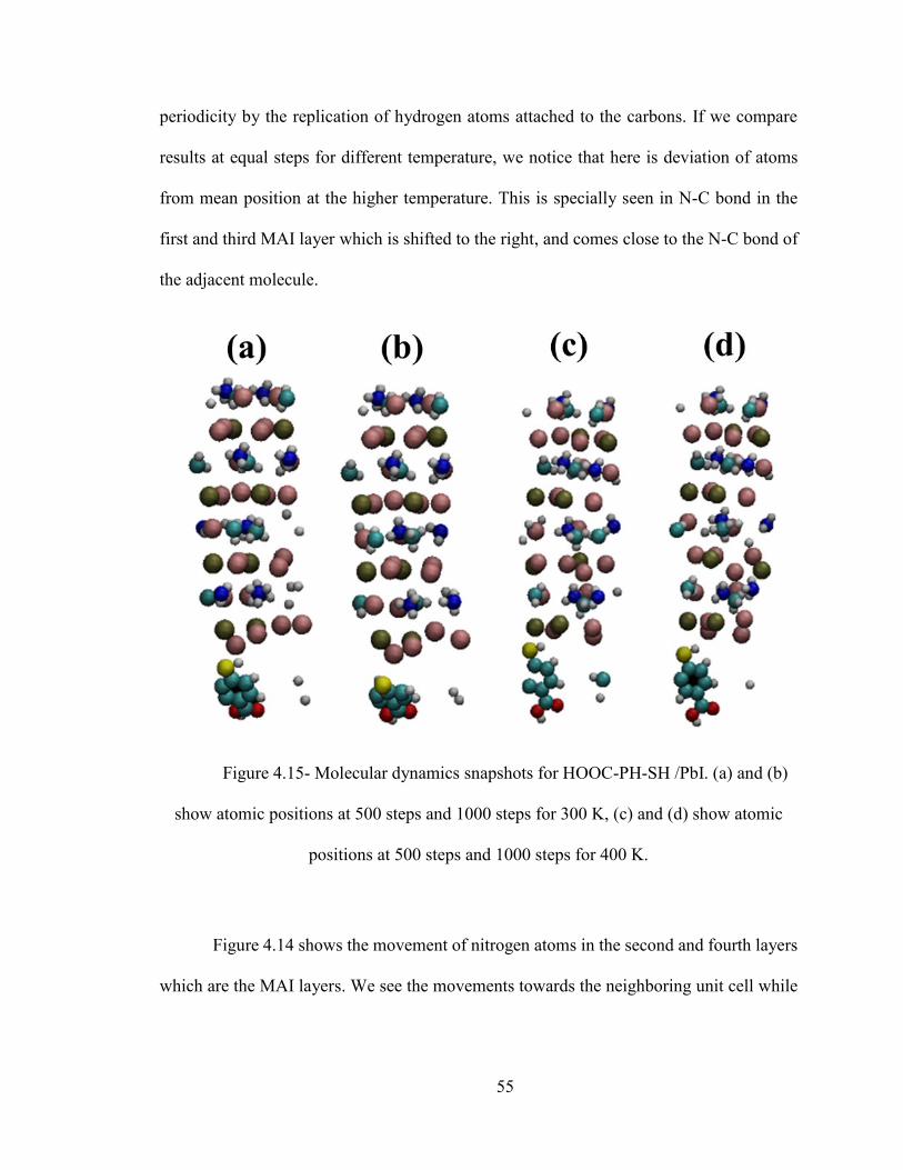
55
periodicity by the replication of hydrogen atoms attached to the carbons. If we compare
results at equal steps for different temperature, we notice that here is deviation of atoms
from mean position at the higher temperature. This is specially seen in N-C bond in the
first and third MAI layer which is shifted to the right, and comes close to the N-C bond of
the adjacent molecule.
Figure 4.15- Molecular dynamics snapshots for HOOC-PH-SH /PbI. (a) and (b)
show atomic positions at 500 steps and 1000 steps for 300 K, (c) and (d) show atomic
positions at 500 steps and 1000 steps for 400 K.
Figure 4.14 shows the movement of nitrogen atoms in the second and fourth layers
which are the MAI layers. We see the movements towards the neighboring unit cell while
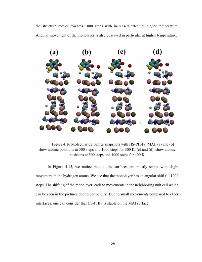
56
the structure moves towards 1000 steps with increased effect at higher temperature.
Angular movement of the monolayer is also observed in particular at higher temperature.
Figure 4.16 Molecular dynamics snapshots with HS-PH-F5 /MAI. (a) and (b)
show atomic positions at 500 steps and 1000 steps for 300 K, (c) and (d) show atomic
positions at 500 steps and 1000 steps for 400 K
In Figure 4.15, we notice that all the surfaces are mostly stable with slight
movement in the hydrogen atoms. We see that the monolayer has an angular shift till 1000
steps. The shifting of the monolayer leads to movements in the neighboring unit cell which
can be seen in the pictures due to periodicity. Due to small movements compared to other
interfaces, one can consider that HS-PHF5 is stable on the MAI surface.

57
Figure 4.17- Molecular dynamics snapshots with HS-PH-F5 /PbI. (a) and (b) show
atomic positions at 500 steps and 1000 steps for 300 K, (c) and (d) show atomic
movements at 500 steps and 1000 steps for 400 K
If we compare Figure 16 (a) through (d), we see that the monolayer has an angular
shift which can be witnessed by the movements in the neighboring unit cell in the pictures
due to periodicity. The monolayer becomes planar at 400 K after 1000 steps. In this
arrangement, there is evidence of reorientation in perovskite. In layer 1 that is the PbI layer,
we see the movements of iodine atoms along Z direction and movements of lead atoms in
horizontal plane when it reaches 1000 steps at 400 K. Similarly, the iodine atoms in layer
2 and lead atoms in layer 3 show clear movement at 400 K.
58
CHAPTER 5 CONCLUSIONS
We study adsorption of two monolayers, HOOC-PH-SH and HS-PH-F5, on
different hybrid perovskite surfaces to form interfaces between the active perovskite
material and hoe/electron transport electrodes. In experiments, it has been shown that
formation of such monolayers improves the performance of hybrid-perovskite-based solar
cell. Using ab initio computer simulations allows us to investigate structural and electronic
features of these interfaces with atomistic resolution. We further perform ab initio
molecular dynamics to assess stability of the interfaces at 300 and 400 K.
Our results based on optimized interface structures show that the average
electrostatic potentials of the monolayers are higher than that of the perovskite material.
This suggest less efficient direct charge transfer at the interface as compared to direct
attachment of, e.g., TiO2 electrode to the perovskite material. This highlights the possibility
of other performance-improving factors caused by adsorbed monolayers as reasons for
experimentally observed improvements. These reasons include better structural match
between the hybrid perovskite and the electrodes (and reduction of interface defects that
can cause charge trapping), better growth conditions for perovskite on monolayers
compared to direct growth on electrodes, optimization of tunneling at the interface towards
charge transfer balance and prevention of corresponding charge accumulation in
perovskite. The hydrophobic monolayers also protect against adverse effects of moistures
Based on charge transfer results and ab initio molecular dynamics simulations at
300 and 400 K, the monolayer adsorptions are considered to be generally stable. Density
of states indicate no adverse effect on charge carrier excitation owing to the monolayers.

59
REFERENCES
[1] M. Hosenuzzaman, N-A. Rahim, J. Selvaraj, M. Hasanuzzaman, A-B-M-A. Malek, A.
Nahar, Global prospects, progress, policies, and environmental impact of solar
photovoltaic power generation, Renewable and sustainable energy reviews, 41, 284-297.
(2015).
[2] S. Sharma, K-K. Jain, A. Sharma, Solar Cells: In Research and Applications—A
Review. Mater Sci Appl, 6, 1145-1155. (2015)
[3] K. Mahmood, S. Sarwarb and M-T. Mehranb, Current status of electron transport
layers in perovskite solar cells: materials and properties, RSC Adv., 7, 17044–17062.
(2017).
[4] Y. Okamoto, Y Suzuki, Perovskite-type SrTiO3, CaTiO3 and BaTiO3 porous film
electrodes for dye-sensitized solar cells, J. Ceram. Soc. Jpn, 122, 728-731, (2014).
[5] W. Geng, C-J. Tong, J. Liu, W. Zhu, W-M. Lau and L-M.Liu, Structures and Electronic
Properties of Different CH3NH3PbI3/ TiO2 Interface: A First-Principles Study, Sci. Rep.
6, 20131 (2016).
[6] J. Cao, J. Yin, S. Yuan, Y. Zhao, J. Lib and N. Zheng, Thiols as interfacial modifiers
to enhance the performance and stability of perovskite solar cells, Nanoscale, 7,
9443.(2015).
[7] G. Park, High Efficiency Mesoscopic Organometal Halide Perovskite Solar Cells, In
Unconventional Thin Film Photovoltaics. London, Royal Society of Chemistry, pp. 1-31,
(2016).

60
[8] David J. Griffiths. Introduction to Quantum Mechanics (Second Edition), Prentice Hall
(2005).
[9] F. Han, J. Luo, B. Zhao, Z. Wan, R. Wang, C. Jia, Cesium Iodide Interface modification
for High efficiency, High stability and Low Hysteresis Perovskite Solar Cells, Electrochima
Acta, 236 , 122-130, (2017).
[10] C-Y. Chang, Y-C. Chang, W-K. Huang, W-C. Liao, H. Wang, C. Yeh, B-C. Tsai, Y-
C. Huang and C-S. Tsao, Achieving high efficiency and improved stability in large area
ITO-free perovskite solar cells with thiol-functionalized self-assembled monolayer, Royal
society of chemisty,4,7903-7913,(2016).
[11] R-O. Jones and O. Gunnarsson, Rev. Mod. Phys. 61, 689 (1989).
[12] J. P. Perdew and Y. Wang, Phys. Rev. B 46, 12947 (1992).
[13] J. P. Perdew and A. Zunger, Phys. Rev. B 23, 5048 (1981).
[14] D-M. Ceperley and B-J. Alder, Phys. Rev. Lett. 45, 566 (1980).
[15] M-C. Payne, M-P. Teter, D-C. Allan, T-A. Arias and J-D. Joannopoulos, Rev. Mod.
Phys. 64, 1045 (1992).
[16] A-D. Becke, J. Chem. Phys. 38, 3098 (1988).
[17] J-P. Perdew, K. Burke, and M. Ernzerhof, Phys. Rev. Lett. 77, 3865 (1996)
[18] J-P. Perdew, K. Burke, and M. Ernzerhof, Phys. Rev. Lett. (E) 78, 1396 (1997).
[19] Blöchl, P.E, Projector augmented-wave method, Phys Ref B, 50, 17953–17978,
(1994).

61
[20] N. A. W. Holzwarth, G. E. Matthews, R. B. Dunning, A. R. Tackett, and Y. Zeng,
Phys. Rev. B 55, 2005-2017 (1997)
[21] G. Kresse and J. Hafner. “Ab initio molecular dynamics for liquid metals”. Phys.
Rev. B, 47,558 (1993).
[22] G. Kresse and J. Hafner. “Ab initio molecular dynamics simulation of the liquid-metal-
amorphous-semiconductor transition in germanium”. Phys. Rev. B, 49, 14251 (1994).
[23] G. Kresse and J. Furthmu¨ller. “Efficiency of ab-initio total energy calculations for
metals and semiconductors using a plane-wave basis set”. Comput. Mat. Sci., 6-15 (1996).
[24] G. Kresse and J. Furthmu¨ller. “Efficient iterative schemes for ab initio total-energy
calculations using a plane-wave basis set”. Phys. Rev. B, 54, 11169 (1996).
[25] W-H. Press, B-P. Flannery, S-A. Teukolsky and W-T. Vetterling, em Numerical
Recipes, (Cambridge University Press, New York, (1986).
[26] G. Kresse, M. Marsman and J- Furthmu¨ller, “VASP the GUIDE”. (2016).
[27] C. C. Stoumpos, C. D. Malliakas, and M. G. Kanatzidis, “Semiconducting Tin and
Lead Iodide Perovskites with Organic Cations: Phase Transitions, High Mobilities, and
Near-Infrared Photoluminescent Properties”. Inorg. Chem, 52 (15), 9019–9038 (2013).
[28] Takeo Oku, “Crystal Structures of CH3NH3PbI3 and Related Perovskite Compounds
Used for Solar Cells”, InTech, 10.5772/59284, (2015).
[29] I. Deretzis, A.L. Magna, Exploring the orthorhombic–tetragonal phase transition in
CH3NH3PbI3: the role of atom kinetics, Nanoscale, 9, 5896-5903 (2017).

62
[30] A.L Montero-Alejo, E. Menendez-Proupin, D. Hidalgo-Rojas, P. Palacios, P.
Wahnon, J.C Conesa, “Modeling of Thermal Effect on the Electronic Properties of
Photovoltaic Perovskite CH3NH3PbI3: The Case of Tetragonal Phase”, J. Phys. Chem. C,
120 (15), pp 7976–7986 (2016).
[31] P. Koirala, B. Kiran, A.K. Kandalam, C.A. Fancher, H.L. de Clercq, X. Li, K.H.
Bowen,”Structural evolution and stabilities of neutral and anionic clusters of lead sulfide:
Joint anion photoelectron and computational studies ”, J. Chem. Phys, 135 ,134311 (2011)
[32] CHR. Rommming,”The crystal structure of 1:1 Addition Compound formed by Benzyl
Sulphide and Iodide” Acta Chemica Scandinavica,14, 2145-2151 (1960).
[33] A. Hordvik, E. Sletten, “The crystal and molecular structure of 4 Phenyl-1,2-
dithiolium Iodide”, Acta Chemica Scandinavica, 20, 1874-1884 (1966).
[34] N. Trinajstic,”Calculation of Carbon Sulphur bond lengths” Tetrahedron Letters, 12,
1529-1532 (1968).
[35] S.C. Nyburg,”Bond Order-bond length correlations for SN bonds in Organic
Molecules”, J. Crystal. Mol. Struct,3, 331-336 (1973).
[36] S. Emami,L. Andrade,A. Mendes,”Recent progress in long term stability of perovskite
solar cells”, U. Porto Journal Of Engineering, 1:2, 52-62 (2015)
[37] Dr. S. Almsoni, L. Cojocaru, D. Li, S. Uchida, T. Kubo, H. Segawa,” Tunneling-
Assisted Trappingas one of the Possible Mechanisms for the Origin of Hysteresis in
Perovskite Solar Cells”, Energy Technol,5,1767-1774 (2017).

63
[38] D. H. Song, M. H. Jang, M. H. Lee, J. H. Heo, J.K. Park, S.J. Sung, D. H. Kim, K.H.
Hong, S.H. Im, “A discussion on the origin and solutions of hysteresis in perovskite hybrid
solar cells” J. Mater. Chem,5, 2883 (2017).
[39] Y. Cheng, H.W. Li, J. Quing, Q. D. Yang, Z. Guan, C. Liu, S. H. Cheung, S. K. So,
C.S. Lee, S.W. Tsang, “The detrimental effect of excess mobile ions in planar CH3NH3PbI3
perovskite solar cells”, J. Mater. Chem. A, 4, 12748-12755(2016).