conjugated polymer electrochromic and light-emitting...
TRANSCRIPT

1
CONJUGATED POLYMER ELECTROCHROMIC AND LIGHT-EMITTING DEVICES
By
AUBREY L. DYER
A DISSERTATION PRESENTED TO THE GRADUATE SCHOOL OF THE UNIVERSITY OF FLORIDA IN PARTIAL FULFILLMENT
OF THE REQUIREMENTS FOR THE DEGREE OF DOCTOR OF PHILOSOPHY
UNIVERSITY OF FLORIDA
2007
2
© 2007 Aubrey L. Dyer

3
To Nathan

4
ACKNOWLEDGMENTS
I can honestly say that this process has been one of the most difficult that I have yet to go
through. It’s not that the Ph.D. process is inherently hard, just the emotional toll that conducting
research while trying to obtain a degree, and remain a sane person, takes on you. There’s the
good days, the bad days, the times of self-doubt, the considerable amount of stress you put on
yourself, and the challenges of working so closely with other people who, while going through
the same process, are so different from yourself. I feel that to successfully get through this with
your spirit still intact, you need strong support from others in your life. I am happy to say that
there have been many people along the way who have fulfilled that role and I would like to say
thanks.
The one person who has been there through it all and never once let me give in and give up
has been Nathan Dyer, my husband. He understood how important this degree is and, while not
able to relate to what I was going through, stood by me and did everything he could to show
support, understanding, and most of all, patience. Another person who has been there and who I
could not have done this without is my advisor, John Reynolds. His ability to relate with every
single person in the group on a personal level is one of the things that sets him apart from most
advisors. He not only keeps the group running by securing funding and keeping the research we
do relevant, but also ensures we, as individuals, are making progress in our research, our
professional lives and our personal lives. He is the group cheerleader, and his level of
enthusiasm for what he does and we do is infectious and it’s what makes this group great to work
in.
I would like to thank the many people who I’ve worked with on various projects over the
years: Christophe Grenier, Ben Reeves, and Bob Brookins. Thanks for handing over your
“babies” to me to tinker with in the lab. I’d also like to thank Dr. Tanner for the optics

5
discussions, Evan Donoghue and Ken Graham for putting the time into designing and fabricating
the “black box”. Special thanks to Nate Heston for the hard work and effort in keeping the
glovebox in such good shape and the evaporator running for me. A final thanks to Evan, and
Eric Shen for volunteering their expertise at the 11th hour in order to help me make sure I get this
done. Thanks Evan for the AFM measurements, and Eric for the distillation. You guys were
there when I really needed help. Also, thanks to my friend Jack for the early morning coffee
breaks.
Over the past five years, there have been a large number of people come and go from the
group and each individual has leant their personality to the dynamics of the Reynolds group and
the Polymer Floor in general. I would like to thank those who have been there for me, as either a
shoulder to cry on, an ear to listen, or just to make me laugh. These people include the MCCL
orphans (Nate Heston, and Ece Unur), Emilie Galand, Sophie Bernard, Maria Nikolou, Cheryl
Googins, Genay Jones, and Gena Borrero. In addition, I’d like to thank my friends Heshan
“Grasshopper” Illangkoon, Dr. Mike Bowen, and Susan Bongiolatti. Looking back, I still can’t
believe some of the things we’ve been a part of on this campus. It was fun and I could honestly
say, a valuable eye-opening experience. I’d also like to thank the many people who I’ve
encountered over the past five years (in the research lab and across campus) who have, in some
way or another, taught me valuable lessons. Some have taught me how to be a good person and
a great friend, others have taught me patience and understanding, probably some of the most
valuable things I’ve received from this education and of which I’m still learning. Finally, I’d
like to thank my family: my mother, Sheila Dedrickson, my sister, Stevie, and my brother,
Shaun.

6
TABLE OF CONTENTS page
ACKNOWLEDGMENTS ...............................................................................................................4
LIST OF FIGURES .........................................................................................................................8
ABSTRACT...................................................................................................................................11
CHAPTER
1 DOPED CONJUGATED POLYMERS IN DISPLAY DEVICES ........................................15
Introduction.............................................................................................................................15 Electrochromism.....................................................................................................................17 Electrochromic Devices..........................................................................................................22 Light-Emitting Devices of Doped Polymers ..........................................................................26 Dual-Purpose Devices ............................................................................................................32
2 REFLECTIVE ELECTROCHROMIC DEVICES OF DISUBSTITUTED POLY(PRODOTS) AS VARIABLE OPTICAL ATTENUATORS......................................36
Reflective Device Construction..............................................................................................36 Unsymmetrical Switching ......................................................................................................39 Conductive Front ....................................................................................................................44 Reflective ECDs as Variable Optical Attenuators..................................................................50 Conclusions.............................................................................................................................58
3 ELECTROCHROMIC DISPLAYS OF MEH-PPV AND CARBAZOLE-CONTAINING COPOLYMERS ...........................................................................................60
Electrochromism of MEH-PPV..............................................................................................62 Electrochromism of Cbz2-Fl2 ................................................................................................65 Electrochromism of Cbz2-Ph3 ...............................................................................................68 Reflective Electrochromic Displays .......................................................................................70 Conclusions.............................................................................................................................78
4 DUAL ELECTROCHROMIC/ELECTROLUMINESCENT DISPLAYS ............................80
Polymer LEDs ........................................................................................................................83 Polymer LECs.........................................................................................................................89 Dual EC/EL ............................................................................................................................99 Overview and Future Directions...........................................................................................104
5 INSTRUMENTATION AND EXPERIMENTAL TECHNIQUES.....................................107
Chemicals and Materials.......................................................................................................107

7
Device Construction .............................................................................................................109 Electrochromic Displays ...............................................................................................109 Polymer Light-Emitting Diodes ....................................................................................111 Polymer Light-Emitting Electrochemical Cells ............................................................111 Dual Electrochromic/Electroluminescent Devices........................................................112
Electrochemical Methods .....................................................................................................113 Electropolymerization ...................................................................................................113 Polymer Electrochemistry .............................................................................................114
Optical Methods....................................................................................................................114 Spectroelectrochemistry ................................................................................................114 Electroluminescence Measurements .............................................................................116
APPENDIX
A POLYMER STRUCTURES.................................................................................................117
LIST OF REFERENCES.............................................................................................................117
BIOGRAPHICAL SKETCH .......................................................................................................129

8
LIST OF FIGURES
Figure page 1-1. Geometric structure of a thiophene trimer showing the allowed electronic transitions. ...18
1-2. Spectroelectrochemical series for a film of poly(3,4-ethylenedioxythiophene) (PEDOT). ...........................................................................................................................19
1-3. Schematic of a typical absorptive/transmissive electrochromic polymer window............23
1-4. Schematic of a typical absorptive/reflective electrochromic polymer display. .................25
1-5. Schematic diagram of a PLED in forward bias showing charge injection, carrier transport, and recombination, with a focus on the two possible methods for charge injection..............................................................................................................................27
1-6. Energy-level diagram, relative to vacuum, for the materials used in a typical PLED.......28
1-7. Schematic of a typical PLED.............................................................................................29
1-8. Schematic of PLEC device operation. ...............................................................................31
2-1. Schematic of a reflective ECD and photographs of a PProDOT-(CH2OEtHx)2 reflective ECD when fully reduced and fully oxidized. ....................................................37
2-2. Reflectance spectroelectrochemistry of a 236 nm thick PProDOT-(CH2OEtHx)2 film in a reflective ECD.............................................................................................................39
2-3. Reflectance spectroelectrochemistry of a 750 nm thick PProDOT-(CH2OEtHx)2 film in a reflective ECD.............................................................................................................40
2-4. Percent reflectance versus cell potential for a 450 nm thick PProDOT-(CH2OEtHx)2 film reflective ECD, and transmittance versus potential for a film of the same polymer and thickness on ITO-glass in 0.2 M TBAPF6/PC electrolyte. ...........................41
2-5. Percent reflectance versus cell potential for a 181 nm thick PProDOT-(CH2OEtHx)2 film reflective ECD demonstrating the lack of unsymmetrical switching in the thinner films. ......................................................................................................................42
2-6. Reflectance spectroelectrochemistry for a 998 nm thick electropolymerized PProDOT-(CH2OEtHx)2 film in an ECD and transmittance spectroelectrochemistry for a film of the same thickness on ITO-glass in 0.2 M TBAPF6/PC................................43
2-7. Percent reflectance versus cell potential for reflective ECDs of electrochemically polymerized PProDOT-(CH2OEtHx)2 of thickness 111 nm, 538 nm, and 998 nm...........43

9
2-8. Percent reflectance versus cell potential for a 351 nm spray-cast film of PProDOT-Hx2 in a reflective ECD and percent transmittance versus potential for a film of the same thickness on ITO-glass in 0.2 M TBAPF6/PC. .........................................................44
2-9. Conductive front model. ..................................................................................................454
2-10. Schematic of multilayer geometry used in analysis of penetration depth of optical radiation through the polymer sample. ..............................................................................48
2-11. Optical attenuation at various applied potentials for a 750 nm thick film of PProDOT-(CH2OEtHx)2 in a reflective ECD as an EC-VOA at the wavelengths of 550, 1310, and 1550 nm.....................................................................................................55
2-12. Schematic of setup to measure reflective EC-VOA using fiber-optic spectrophotometer and photograph of actual holder with fiber-optics in place.................56
2-13. Optical attenuation across the wavelength range of 1.3 µm and 1.55 µm for a 450 nm thick film of PProDOT-(CH2OEtHx)2 in a reflective ECD as an EC-VOA measured using the fiber-optic setup..................................................................................................57
2-14. Optical attenuation at 1.55 µm and 550 nm of a 450 nm thick film of PProDOT-(CH2OEtHx)2 in a reflective ECD as an EC-VOA. ...........................................................58
3-1. Diagram of oxidation potentials (vs. SCE) for several electrochromic and electroluminescent polymers relative to the level required for air stability along with optical bandgap values.......................................................................................................61
3-2. Structures of polymers studied...........................................................................................62
3-3. Cyclic voltammograms of a drop-cast film of MEH-PPV on ITO/glass at a scan rate of 30 mV/s switched in 0.2 M LiOTf/ACN for 50 cycles. ................................................63
3.4. Spectroelectrochemistry of a drop-cast film of MEH-PPV on ITO/glass switched in 0.2 M LiOTf/ACN and photographs of the same film held at potentials indicated...........64
3-5. Cyclic voltammograms of a spray-cast film of Cbz2-Fl3 on ITO/glass switched at 30 mV/s in 0.2 M LiOTf/water for 50 scans...........................................................................66
3-6. Spectroelectrochemistry of spray-cast film of Cbz2-Fl2 on ITO/glass in 0.2 M LiOTf/water and photographs of the same film held at various potentials........................67
3-7. Cyclic voltammograms of a spray-cast film of Cbz2-Ph3 on ITO/glass at a scan rate of 30 mV/s in 0.2 M LiOTf/water for 5 scans. ..................................................................68
3-8. Spectroelectrochemistry of a spray-cast film of Cbz2-Ph3 on ITO/glass in 0.2 M LiOTf/water. ......................................................................................................................69
10
3-9. Schematic of reflective electrochromic displays with porous white diffuse reflector and aluminum-coated porous membrane. ..........................................................................71
3-10. Reflectance spectroelectrochemistry of spray-cast PProDOT-(CH2OEtHx)2 in an electrochromic display with a porous white reflector and aluminum-coated porous membrane...........................................................................................................................73
3-11. Spectroelectrochemistry and photographs of MEH-PPV/PEO/LiOTf blend reflective ECD with porous white reflector and spectroelectrochemistry and photographs of MEH-PPV/PEO/LiOTf blend reflective ECD with aluminum-coated membrane. ...........76
3-12. Spectroelectrochemistry of Cbz2-Fl2/LiOTf blend reflective ECD with a porous white reflector and aluminum-coated membrane. .............................................................78
4-1. Schematic of measurement geometry between fiber-optic probe and PLED pixel. ..........85
4-2. Spectral irradiance of an ITO/PEDOT:PSS/70 nm MEH-PPV/Ca/Al PLED at different applied voltages. Inset shows a photograph of pixel at 9 V...............................84
4-3. Current density and luminance versus applied voltage for an average of 4 pixels of an ITO/PEDOT:PSS/70 nm MEH-PPV/Ca/Al PLED.......................................................89
4-4. Current density and luminance versus applied voltage for an ITO/blend/Al PLEC with an active layer of a blend of MEH-PPV:PEO:LiOTf in a weight ratio of 10:3:1......92
4-5. Current density and luminance versus applied voltage for an average of 3 pixels of an ITO/MEH-PPV blend/Al PLEC....................................................................................93
4-6. Spectral irradiance of an ITO/170 nm MEH-PPV:PEO:LiOTf blend/Al PLEC pixel at different applied voltages. Inset shows photograph of pixel operated at -6 V..............94
4-7. Luminance and current density as a function of applied voltage for an ITO/blend/Al PLEC with an active layer of a blend of MEH-PPV:PEO:LiOTf cycled between 0V and -8 V for three cycles. ...................................................................................................95
4-8. Integrated spectral irradiance over the wavelength range of 400 and 800 nm for a LEC pixel operated for 13 continuous hours at -6V. The inset shows the spectral response in the first 2 minutes of operation. ......................................................................96
4-9. Comparison of the J-V and L-V response of two LECs constructed with PEO dried to different extents. ............................................................................................................99
4-10. Schematic of dual EC/EL device and photograph of actual device.................................101
4-11. Photographs of a dual electrochromic and light-emitting device with MEH-PPV as the active material. ...........................................................................................................103
4-12. Schematic of proposed lateral dual EC/EL device. .........................................................106

11
LIST OF ABBREVIATIONS
ACN: Acetonitrile.
Eg: Bandgap energy.
Cbz: Carbazole.
CB: Conduction band.
EC: Electrochromic.
ECD: Electrochromic display.
EL: Electroluminescent.
Fl: Fluorene.
ITO: Indium-doped tin oxide.
LiOTf: Lithium trifluoromethanesulfonate.
MEM: Microelectromechanical.
OLED: Organic light-emitting display.
Ph: Phenylene.
PAc: Polyacetylene.
PEDOT: Poly(3,4-ethylenedioxythiophene).
PEO: Poly(ethylene oxide).
PLED: Polymer light-emitting diode.
PLEC: Polymer light-emitting electrochemical cell.
PMMA: Poly(methylmethacrylate).
PPV: Poly(para-phenylenevinylene).
PProDOP: Poly(3,4-propylenedioxypyrrole).
PProDOT: Poly(3,4-propylenedioxythiophene).
PSS: Poly(styrenesulfonate).
12
PC: Propylene carbonate.
SWNT: Single-walled carbon nanotubes.
VB: Valence band.
VOA: Variable optical attenuator.
13
Abstract of Dissertation Presented to the Graduate School of the University of Florida in Partial Fulfillment of the Requirements for the Degree of Doctor of Philosophy
CONJUGATED POLYMER ELECTROCHROMIC AND LIGHT-EMITTING DEVICES
By
Aubrey L. Dyer
December 2007
Chair: John R. Reynolds Major: Chemistry
Conjugated conducting polymers are among some of the most versatile materials to
emerge in the past 20 years. They have been researched for applications that range from
photovoltaics, to light-emitting diodes, electrochromic windows, actuators, and field effect
transistors. This work details the analytical characterization of π-conjugated polymers to
understand their redox and optical properties, along with the development of several new types
of devices that employ these polymers as the active materials for both variable optical attenuators
and as dual electrochromic/electroluminescent displays. Within this work, a phenomenon that
we term unsymmetrical switching has been uncovered for the first time in reflective
electrochromic cells. The unsymmetrical switching in these displays is explored and a model
devised to illustrate that the presence of a conductive front propagating through the polymer film
on electrochemical oxidation is the contributing cause for this observation. For these
experiments, a variety of analytical techniques have been utilized to characterize the devices and
materials contained therein and include electrochemistry, spectroelectrochemistry, and
photometry.
The first application utilizes the large near infrared electrochromic contrasts of some
dioxythiophene-based polymers when incorporated in reflective electrochromic displays. For the

14
first time, it is demonstrated that these devices can be utilized as electrochromic variable optical
attenuators, important components for the optical telecommunications industry, exhibiting
optical attenuation values of 12 decibels while maintaining optical loss values, in the off state, as
low as 0.1 decibels. These devices offer the benefit of yielding mechanically flexible,
miniaturized electrochromic variable optical attenuators that operate with a low drive voltage (±
1.2 volts).
A new concept is also introduced for conjugated conducting polymers as the active
material in dual electrochromic/electroluminescent displays that are unique in that a single active
polymer film is employed as both the emitter and electrochrome. In using a soluble para-
phenylene-vinylene-based polymer, a device is developed that shows orange to blue
electrochromism and orange-red electroluminescence from the same pixel. This type of device
potentially fulfills a need in the display industry for a device that exhibits light emission in low
ambient lighting while maintaining a high optical contrast, without sacrificing image quality, in
directly lit situations. This device also offers the possibility of a flexible, patterned display as
desired in the consumer electronics industry.
15
CHAPTER 1 DOPED CONJUGATED POLYMERS IN DISPLAY DEVICES
Introduction
The field of conducting polymers can be dated to as far back as 1862 when Letheby
described the production of a dark green film on an electrode when oxidizing aniline under
acidic conditions.1 The most studied conducting polymer, polyactetylene (PAc), can even be
dated to 1955 when Natta produced the polymer using the coordination catalyst system
commonly used to polymerize ethylene and propylene.2 PAc was even found to behave as a
semiconductor by various researchers in the 1960s on treatment with reagents such as boron
trifluoride and ammonia, producing dramatic changes in conductivity.3-6 It was not until the
1970s when Shirakawa and coworkers improved the procedure for the synthesis of PAc,7, 8
combined with further work by Heeger and MacDiarmid,9-11 that the field of conducting
polymers really emerged with PAc established as the first conducting organic polymer.
In their work, Heeger, MacDiarmid, and Shirakawa demonstrated that the conductivity of
PAc films increased many orders of magnitude on exposure to halogen vapors.10 Other
researchers have also demonstrated that reacting PAc with oxidants (e.g., I2, Fe(ClO4)3) or
reductants (e.g., NaC10H8), forms highly conducting derivatives of PAc. 12, 13 These reactions are
called “doping”, analogous to terminology used in semiconductor physics with p-doping an
oxidative reaction, with insertion of charge-balancing anions, and n-doping a reduction with
insertion of charge-balancing cations. The two most commonly used methods for chemical
doping are exposing the polymer to a gas-phase dopant, such as iodine vapors, or a solution of
the dopant, such as SbCl5, diluted in an appropriate solvent.14 The rate of doping and maximum
doping level can be controlled by dopant concentration and exposure time.

16
While chemical doping has been instrumental in initial demonstrations of the theoretical
and technological promise of PAc by allowing tunable conductivity of the polymer film from the
semiconducting to the metallic regime, the applicability of this method is lacking. In many
cases, the chemical dopants are highly reactive and difficult to handle, not allowing for the
utilization of these polymers outside the research laboratory. In 1979, Nigrey and coworkers
demonstrated that PAc could be reversible p- or n-doped electrochemically, but the material’s
instability remained as an obstacle to commercial applications.15 The neutral polymer is not air
stable and decomposes quite rapidly and therefore must be handled in an inert atmosphere and is
additionally difficult to process with melt processing resulting in degradation.
It was not until that same year when Diaz et al., electrochemically polymerized pyrrole to
produce free-standing, air-stable polymer films that had conductivities of 100 Ω-1cm-1.16, 17 The
method they used was a modification of that originally reported by Dall’Olio in 1968 with the
main difference being that Diaz et al, obtained continuous films that could be peeled off the
platinum electrodes as opposed to a powdery, insoluble precipitate.18 Not only did this
demonstrate the ability to electrochemically polymerize directly onto an electrode and reversibly
switch the polymer between a neutral and oxidized state, but it introduced the field to
polyheterocycles, which would become the most important class of conducting polymer to date.
The impact of pyrrole systems stems from several factors that include chemical and thermal
stability of the polymers, the ease of preparation of polymer films, and the ability to synthesize
derivatives that allow for modification of the electrical and physical properties of the final
polymer.
This opened the door for other electrochemically active polymer systems to enter the field
and demonstrate their applicability as the active materials in areas ranging from batteries,
17
capacitors,19 light-emitting displays,20 field-effect transistors,21 electrochromic displays,22 solar
cells,23 and actuators.24 Conducting polymers hold much promise for these, and many other,
applications as they allow tuning of physical and electronic properties through structural
modification of the polymer backbone; a feature not available in any other material. This
introduction will cover two applications of doped conjugated polymers (electrochromism and
light-emission), the methods by which these physical processes occur and the types of devices in
which they are employed.
Electrochromism
Electrochromics are materials that can induce a reversible change in the absorption,
reflection, or transmission of optical radiation when the material is involved in an
electrochemical reductive or oxidative process.25 Electrochromism not only includes changes in
the visible region, but also in the ultraviolet (UV), infrared (IR), and even the microwave regions
of the spectrum.26-28 Some of the most commonly researched electrochromes are those based on
transition metal oxides (e.g., tungsten oxide, WO3), 4,4’-bipyridinium salts (e.g., methyl
viologen), and polynuclear transition metal hexacyanometallates (e.g., Prussian Blue,
[FeIIIFeII(CN)6]-).29-35
Over the past two decades, conjugated polymers have emerged as one of the most
promising electrochromic materials available.22 This is due to the fact that they offer color
tunability, faster switching, and improved processability over the inorganic and molecular
electrochromes mentioned. Electrochromism in conjugated conducting polymers arises from the
polymer’s bandgap and any midgap states created on doping. The optical bandgap is determined
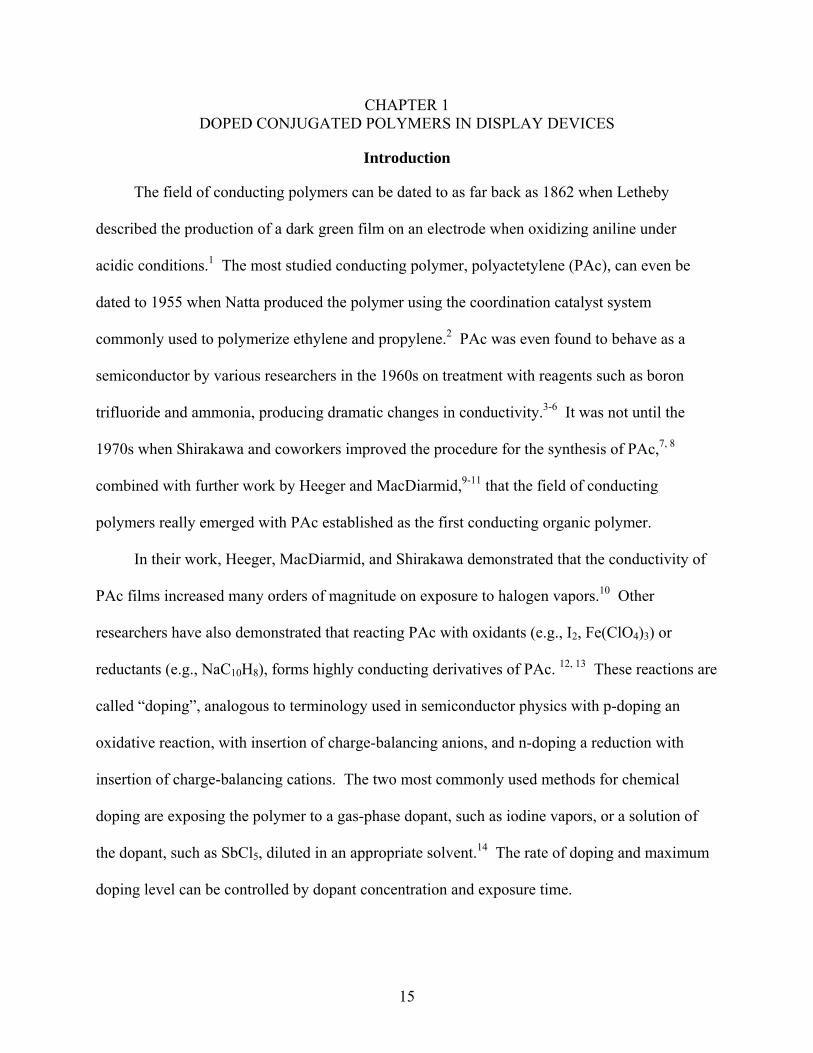
by the onset of the π-π* transition of the polymer in the neutral, undoped state and is the
electronic transition, as shown in Figure 1-1A, that occurs with the minimum energy difference
from the valence band to the conduction band.
18
Figure 1-1. Geometric structure of a thiophene trimer showing the allowed electronic transitions.
A) Neutral; B) Polaron; C) Bipolaron states. Note: The forbidden transitions are not shown for clarity.
As the polymer is oxidized, electrons are removed from the valence band and lower energy
absorptions begin to emerge in the electronic spectra at the expense of the π-π* transition. This
is due to the removal of the π-electrons from the valence band, creating half-filled polaron levels
that are symmetric about the bandgap center. Figure 1-1B shows the allowed electronic
transitions for these new lower energy states. This newly formed radical cation is delocalized
over a polymer segment and behaves as a polaronic charge carrier. This oxidation induces a
relaxation of the aromatic geometry to a quinoid-like structure in the polymer chain and is
accompanied by a charge balance by the electrolyte anions.
On further oxidation, a dication is formed (with the cations coupled to one another) and is
a bipolaronic charge carrier delocalized over the same polymer segment. As is shown in Figure
1-1C, only electronic transitions from the top of the valence band occur as the bipolaron levels
are unoccupied. At this point, only lower energy absorptions are seen in the electronic spectra,
and the π-π* is depleted. This can be seen in Figure 1-2 for the spectroelectrochemical series of
poly(3,4-ethylenedioxythiophene) or PEDOT. The neutral polymer is dark blue as the bandgap

19
is in the visible region at 1.65 electron volts (eV). As the polymer is p-doped, an absorption
emerges in the NIR and the color of the polymer begins to bleach, finally becoming a highly
transmissive sky blue.
Figure 1-2. Spectroelectrochemical series for a film of poly(3,4-ethylenedioxythiophene)
(PEDOT). Dashed arrows show direction of spectral growth or recession.
As mentioned previously, conducting polymers offer the advantage of color tailorability in
the neutral and doped states through synthetic methods. This can be seen when comparing
polythiophene to PEDOT. Unsubstituted polythiophene has a bandgap of 2.0-2.2 eV, switching
from red in the neutral state to blue upon oxidation. However, it is difficult to obtain uniform
polymer films because the polymer overoxidizes at the potentials required for
electropolymerization and side reactions can occur at the β-position causing undesirable
structural defects.36-39 To overcome these issues, research became focused towards substitution
at the 3-position or the 3- and 4-positions of the thiophene ring yielding polymers with bandgaps
that ranged from less than 1 eV to higher than the parent thiophene.
20
One of the most commercially successful polymers to date, PEDOT was produced with the
goal of not only lowering the polymer bandgap, but also exhibit a lower oxidation potential and
higher stability. PEDOT not only has a lower bandgap than the unsubstituted thiophene, it is
also easily oxidized and highly stable in the doped state. This is due to the presence of the
electron-donating oxygens adjacent to the thiophene ring. On oxidation, PEDOT becomes
highly conducting and transmissive in the visible region. However, this polymer has the
drawback of insolubility. To overcome this limitation, the aqueous dispersion of the doped form
of PEDOT with the polyelectrolyte, poly(styrenesulfonate) (PSS), was produced. Cast films of
PEDOT:PSS have greater than 75% transmissivity in the visible region and greater than 120
S/cm film conductivity.40 Applications for this polymer have been mostly for its use as a
conductor for antistatic coatings, solid state capacitors, organic electronic devices, and even as a
transparent electrode material.19, 41-44
Recent synthetic effort has been towards producing polymers, especially those based on
the alkylenedioxythiophenes, that are processable. Through the introduction of alkyl and alkoxy
chains on the propylene bridge, a family of poly(3,4-propylenedioxythiophenes) (PProDOTs) has
been synthesized that is soluble in common organic solvents such as toluene and chloroform.45-48
This allows uniform, thick films to be cast from solution using methods such as drop-casting,
spincoating, spraycoating, and inkjet or screen printing. In addition to the improved
processability, the PProDOTs have faster switching speeds and larger optical contrasts. The
tetrahedral substitution pattern on the propylene bridge causes the alkyl and alkoxy groups to be
positioned above and below the plane of the polymer chain. This allows the polymer chains to
separate, opening up the film for more facile counter ion movement and leading to higher doping
levels. This also hinders π-stacking, causing a decrease in the polymer conductivity.
21
The dioxythiophene family of conjugated polymers are colored in their neutral state and
switch to a highly transmissive state on oxidation and are therefore cathodically coloring.
Another class of polymers are those that are anodically coloring, and highly transmissive when
neutral, switching to colored on oxidation.49-53 The N-substituted alkylenedioxypyrroles are such
a family of polymers with the polymer bandgap shifted into the ultraviolet region of the spectrum
allowing for near-transparency in the neutral state. Substitution at the N-position introduces
steric interactions that vary the degree of π-overlap along the polymer backbone. This induces a
twist in the polymer backbone that causes a decrease in the effective conjugation length leading
to an increase in the bandgap.22, 54, 55 As previous calculations have shown,22 substitution with
the bulky ethoxyethoxyethanol at the N-position in poly(3,4-propylenedioxypyrrole) (PProDOP-
N-Gly) causes a twist angle between the pyrrole rings of 71.6º whereas the unsubstituted
PProDOP is fully planar.
The unsubstituted PProDOP has a bandgap of 2.2 eV and is orange in the neutral state
switching to light gray-blue on oxidation, while PProDOP-N-Gly has a bandgap of 3.4 eV and is
colorless in the neutral state and blue-gray when oxidized. The electron-rich character of the
pyrrole along with the presence of the alkylenedioxy bridge reduces both the monomer and
polymer oxidation potentials. This allows for polymerization to occur under relatively mild
conditions and the polymer to have an increased stability under ambient conditions in the doped
conducting state with the family of PProDOPs having the lowest reported polymer oxidation
potentials to date.50 The anodically coloring properties of the N-substituted PProDOPs along
with the low polymer oxidation potential makes them complementary to the PProDOTs when
both are incorporated into absorptive/transmissive electrochromic windows.53 Additionally, the

22
fast switching speeds, large optical contrasts (in the visible and NIR), and high redox stability of
the PProDOTs makes them ideal for absorptive/reflective electrochromic displays.56, 57
Electrochromic Devices
Electrochromic devices are electrochemical cells in which a redox reaction occurs at a
working electrode and counter electrode by application of an electric field across the device.
Typically, one or more electrochromic materials are deposited on both the working electrode and
counter electrode and the electromagnetic radiation absorbed, transmitted, or reflected from the
device is modulated.29, 58-60 Most commonly, electrochromic materials are deposited as films on
both the working and counter electrodes with the material on the counter electrode acting as a
charge-balancing source for the redox reaction and, in some cases, as a complementary
electrochrome to that at the working electrode. In dual polymer ECDs, both materials are
electrochromic polymers, while in hybrid devices, the material at the counter electrode can be
any other class of electrochromic material and has included Prussian Blue, viologens, and
WO3.61-66
An electrolyte layer is deposited between the two electrodes with the requirement that the
material used have a high conductivity, transparency in the wavelength range measured, wide
window of electrochemical stability, and low volatility. Materials used include gel electrolytes,
solid electrolytes, and ionic liquids.53, 67-71 The electrodes utilized in these devices are dependent
on how the light is to be modulated with reflective metallic electrodes in the absorptive/reflective
devices and transparent electrodes utilized in the absorptive/transmissive devices. The reflective
electrodes can be metallized, porous membranes that allow for ion transport through the
membrane while exhibiting a high specular reflectance.56, 72-74 Metals used include gold,
platinum, and aluminum. Transparent electrodes include indium-doped tin oxide (ITO) on glass,

23
fluorine-doped tin oxide (SnO2:F) on glass, PEDOT:PSS on glass or plastic, and single-walled
carbon nanotubes (SWNT) on glass or plastic.75, 76
Absorptive/transmissive, or window-type, displays operate by reversibly switching the
device between a highly absorptive, colored state and a highly transparent, bleached state. Both
the working electrode and counter are transparent for light to pass with the conductive materials
(ITO, SnO2:F, PEDOT:PSS, or SWNT) deposited on glass or plastic substrates. As is shown in
Figure 1-3, films of two complementary electrochromic materials, one anodically coloring, the
other cathodically coloring, are deposited on the electrodes with a layer of electrolyte
sandwiched in between.
Figure 1-3. Schematic of a typical absorptive/transmissive electrochromic polymer window.
The device becomes highly absorptive when biased with a negative potential applied to the
cathodically coloring electrode and becomes bleached when the bias is reversed. The colors of
the device are additive in that they are a combination of those exhibited by both materials. The
absorptive/transmissive window devices typically operate in the visible region, but recent

24
research towards the production of IR-transparent electrodes (e.g., SWNT) has allowed for the
fabrication of dual polymer devices that operate in the NIR through far-IR regions of the
spectrum.76
The absorptive/reflective electrochromic displays can also operate not only in the visible
region, but also at the longer wavelengths of the NIR and far-IR as most metals utilized as the
working electrode are highly reflective through those regions of the spectrum.47, 56, 57, 72-74 One
type of electrode demonstrated is a gold-coated ion permeable porous membrane. As is shown in
Figure 1-4, this electrode is outward facing, with the active electrochromic material deposited on
top. Behind the electrode is the electrolyte layer and counter electrode. The counter electrode in
this case only acts as a redox-balancing layer, not contributing any optical properties to the
electrochromism of the device. This allows for probing of the electrochromic properties of the
active layer alone. The entire device is encapsulated with a cover window that is transparent to
the wavelengths measured with ZnSe utilized in the NIR to mid-IR, glass for visible to NIR, and
polyethylene for visible to mid-IR.56, 57 As an example, when the active polymer layer is a
cathodically coloring polymer, the device is highly absorptive in the visible region and highly
reflective in the NIR when a negative bias is applied. When the bias is switched, the polymer
becomes oxidized and the device is highly reflective in the visible region, with the metal
electrode visible underneath, and absorptive in the NIR.
Both types of device platforms allow for patterning of not only the electrodes but also the
active electrochromic layer. In window-type devices with PEDOT:PSS as the transparent
conductor, the electrode can be patterned by screen printing, inkjet printing, and micro-contact
printing, not only on glass, but also on a flexible substrate such as plastic.

25
Figure 1-4. Schematic of a typical absorptive/reflective electrochromic polymer display.
Similarly, the metallic conductor in the reflective devices can also be patterned by metal
vapor deposition, or line patterning and micro-contact printing followed by electroless plating.
The polymer layers can then be selectively deposited by electrochemical polymerization onto the
patterned electrode or, with the increasing number of soluble polymers becoming available,
printing by inkjet or screen printing.77-80
The combination of the various device platforms available, along with the versatility of the
electrochromic polymers and the large variety of colors available makes them ideal for most
display applications. While these devices and materials offer enhanced performance over other
electrochromic materials in color tailorability, subsecond switching speeds, optical memory, and
low power consumption, some challenges still exist. These include increasing device lifetime to
that needed in commercial applications by improving environmental stability and decreasing
26
switching speeds to below millisecond rates. Meanwhile, there exist applications where these
issues are not imperative, one of which is applications where the display or device is disposable,
being discarded after only a few uses, for example, and the other is the variable optical attenuator
that will be discussed in detail in this dissertation.
Light-Emitting Devices of Doped Polymers
One of the most highly researched and publicized uses of conjugated conducting polymers
is as the active material in polymer light-emitting displays. In 1987, it was demonstrated that
display-brightness could be achieved for organic light-emitting diodes (OLEDs). These devices
consisted of vacuum-deposited layers of an aromatic diamine and the fluorescent metal chelate
complex 8-hydroxyquinoline aluminum (Alq3).81 A drawback to these materials is that the
requirement of vacuum sublimination of films is difficult to translate to practical commercial
devices.
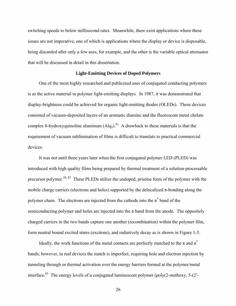
It was not until three years later when the first conjugated polymer LED (PLED) was
introduced with high quality films being prepared by thermal treatment of a solution-processable
precursor polymer.20, 82 These PLEDs utilize the undoped, pristine form of the polymer with the
mobile charge carriers (electrons and holes) supported by the delocalized π-bonding along the
polymer chain. The electrons are injected from the cathode into the π* band of the
semiconducting polymer and holes are injected into the π band from the anode. The oppositely
charged carriers in the two bands capture one another (recombination) within the polymer film,
form neutral bound excited states (excitons), and radiatively decay as is shown in Figure 1-5.
Ideally, the work functions of the metal contacts are perfectly matched to the π and π*
bands; however, in real devices the match is imperfect, requiring hole and electron injection by
tunneling through or thermal activation over the energy barriers formed at the polymer/metal
interface.83 The energy levels of a conjugated luminescent polymer (poly(2-methoxy, 5-(2’-
27
ethyl-hexyloxy)paraphenylene vinylene) (MEH-PPV), and the electrodes used in a typical PLED
are shown in Figure 1-6.
Figure 1-5. Schematic diagram of a PLED in forward bias showing charge injection (a. and c.),
carrier transport (b. and d.), and recombination (e.), with a focus on the two possible methods for charge injection, tunneling and thermal activation.
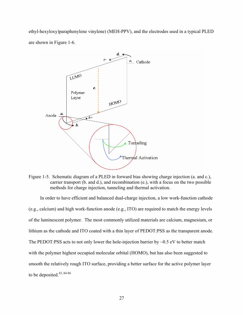
In order to have efficient and balanced dual-charge injection, a low work-function cathode
(e.g., calcium) and high work-function anode (e.g., ITO) are required to match the energy levels
of the luminescent polymer. The most commonly utilized materials are calcium, magnesium, or
lithium as the cathode and ITO coated with a thin layer of PEDOT:PSS as the transparent anode.
The PEDOT:PSS acts to not only lower the hole-injection barrier by ~0.5 eV to better match
with the polymer highest occupied molecular orbital (HOMO), but has also been suggested to
smooth the relatively rough ITO surface, providing a better surface for the active polymer layer
to be deposited.43, 84-86

28
Figure 1-6. Energy-level diagram, relative to vacuum, for the materials used in a typical PLED.
The HOMO and LUMO levels of MEH-PPV87 and the Fermi level positions of the electrodes are shown.
The high-lying lowest unoccupied molecular orbital (LUMO) levels of luminescent
conjugated polymers requires the use of low work-function, and therefore highly reactive, metals
such as calcium, magnesium, or cesium. These metals have been shown to interact with the
organic polymer layer and quench luminescence in addition to interacting with the environment
leading to quick degredation.88, 89 In most cases, the reactive cathode layer is capped with
another metal layer, such as aluminum, to protect the cathode from exposure to oxygen and
moisture. In addition, the operating voltage and efficiency of the device is determined by the
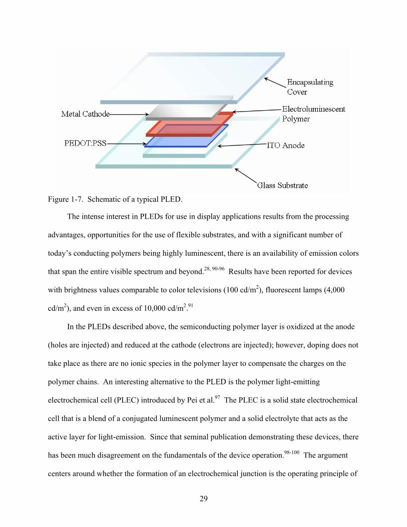
active polymer layer thickness with ideal thicknesses under 100 nm. The typical device layout
for a PLED is shown in Figure 1-7. The device consists of the transparent anode, onto which the
luminescent polymer layer is cast. The metal cathode contacts are then thermally evaporated
onto the polymer layer and the entire device encapsulated to exclude moisture and oxygen.
29
Figure 1-7. Schematic of a typical PLED.
The intense interest in PLEDs for use in display applications results from the processing
advantages, opportunities for the use of flexible substrates, and with a significant number of
today’s conducting polymers being highly luminescent, there is an availability of emission colors
that span the entire visible spectrum and beyond.28, 90-96 Results have been reported for devices
with brightness values comparable to color televisions (100 cd/m2), fluorescent lamps (4,000
cd/m2), and even in excess of 10,000 cd/m2.91
In the PLEDs described above, the semiconducting polymer layer is oxidized at the anode
(holes are injected) and reduced at the cathode (electrons are injected); however, doping does not
take place as there are no ionic species in the polymer layer to compensate the charges on the
polymer chains. An interesting alternative to the PLED is the polymer light-emitting
electrochemical cell (PLEC) introduced by Pei et al.97 The PLEC is a solid state electrochemical
cell that is a blend of a conjugated luminescent polymer and a solid electrolyte that acts as the
active layer for light-emission. Since that seminal publication demonstrating these devices, there
has been much disagreement on the fundamentals of the device operation.98-100 The argument
centers around whether the formation of an electrochemical junction is the operating principle of

30
the device. While not entirely resolved, much recent research has been focused towards this
effort with experimental observations agreeing with this initial model.101, 102
In general, as is shown in Figure 1-8, when a sufficiently high voltage is applied between
the cathode and anode, charges are injected from the electrodes into the luminescent polymer.
Counter ions from the solid electrolyte redistribute to compensate the charges on the oxidized
and reduced polymer chains, and simultaneous electrochemical p- and n-doping occur at the
anode and cathode, respectively. Since the electrical conductivity of doped conjugated polymers
increases significantly on doping, the polymer/electrode interfaces become low-resistance
contacts. Once electrochemical equilibrium is reached in the cell, a p-n junction is formed and
the ionic contribution to the current goes to zero. The electronic contribution to the current, on
the other hand, continues under the influence of the applied voltage with the holes in the π-band
(p-type carriers) and electrons in the π*-band (n-type carriers) migrating through the high-
conductivity doped regions. After a turn-on time, a thin insulating region is formed separating
the doped regions, creating a p-i-n junction, where the charge carriers recombine to form neutral
charge carrier pairs that radiatively decay to the ground state.97, 100, 103-110
Unlike conventional inorganic LEDs, the p-n junction is dynamic in that the device will
discharge after the external bias is removed and the junction will need to be reestablished when
the device is to be once again turned on. Additionally, given the electrical conductivity of
conducting polymers on doping, most of the external bias is applied across the p-i-n junction.
The minimum bias required to maintain the junction is equal to the built-in potential difference
of the p-n junction and is ideally equal to the HOMO-LUMO gap of the polymer.
It can be seen that the turn-on time of a LEC is dictated by the speed of electrochemical
doping of the conjugated polymer and the rate of formation of the p-i-n junction, which are
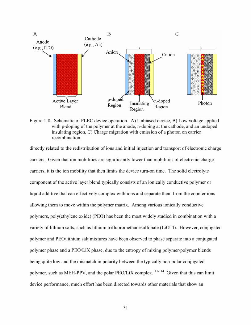
31
Figure 1-8. Schematic of PLEC device operation. A) Unbiased device, B) Low voltage applied
with p-doping of the polymer at the anode, n-doping at the cathode, and an undoped insulating region, C) Charge migration with emission of a photon on carrier recombination.
directly related to the redistribution of ions and initial injection and transport of electronic charge
carriers. Given that ion mobilities are significantly lower than mobilities of electronic charge
carriers, it is the ion mobility that then limits the device turn-on time. The solid electrolyte
component of the active layer blend typically consists of an ionically conductive polymer or
liquid additive that can effectively complex with ions and separate them from the counter ions
allowing them to move within the polymer matrix. Among various ionically conductive
polymers, poly(ethylene oxide) (PEO) has been the most widely studied in combination with a
variety of lithium salts, such as lithium trifluoromethanesulfonate (LiOTf). However, conjugated
polymer and PEO/lithium salt mixtures have been observed to phase separate into a conjugated
polymer phase and a PEO/LiX phase, due to the entropy of mixing polymer/polymer blends
being quite low and the mismatch in polarity between the typically non-polar conjugated
polymer, such as MEH-PPV, and the polar PEO/LiX complex.111-114 Given that this can limit
device performance, much effort has been directed towards other materials that show an

32
improved morphology on blending with luminescent polymers.115-119 Such materials include
crown ethers complexed with various salts. These devices have been demonstrated to show a
higher luminance and longer lifetimes than devices containing the PEO/LiOTf solid electrolyte.
In addition, binary systems of conjugated luminescent polymers containing ion solvating side
groups complexed with a salt and luminescent/ionic liquid blends have gained increasing
attention as there would be no need for an additional ion solvating material and complications
arising from phase separation are decreased.120-126
An important characteristic of the PLEC is that, due to the low resistivity of the doped
polymer and the tendency to form ohmic contacts with the metal electrodes, the performance of
the device is insensitive to the electrode materials. Not only can the use of highly reactive, low
work function cathodes be avoided, but the same metal can be utilized for both anode and
cathode.127-129 Another unique property of LECs includes the fact that light emission can occur
for both forward bias as well as for reverse bias with onset voltages equal in both directions.
Onset voltages have also been demonstrated to be nearly independent of the active layer
thickness. This has been effectively demonstrated by the use of a planar electrode configuration
with two parallel gold electrodes of 1 mm spacing.129 In this case, the light is emitted from
within the zone between the metal contacts.128, 130 Even though these devices have turn-on
voltages at or near the polymer bandgap, while being independent of film thickness and without
the need for highly reactive metal contacts, quantum efficiencies can be achieved that rival those
of PLEDs. As the switching speeds and lifetimes are improved, their impact in the field of light-
emitting displays will be distinct.
Dual-Purpose Devices
Electroactive conjugated polymers can exhibit electrochromism and light-emission, as has
been discussed, but they also have been demonstrated as the active component in many devices
33
such as photovoltaics, actuators, field-effect transistors, and supercapacitors with more than one
of these devices utilizing the same family of polymers. Many of these properties operate on
similar principles or by similar mechanisms. This opens the door for dual purpose devices or
displays that perform multiple functions with the same active material or same device by the
fabrication of creative device architectures.
For example, both electrochromic devices and actuators operate by electrochemical
oxidation or reduction of the polymer film with simultaneous ingress/egress of charge balancing
counterions. With the electrochromic devices, the property desired from this action is the
resulting color change on oxidation/reduction. For the actuator devices, the action is contraction
or expansion of the polymer film due to a volume change from the counter ion movement. A
device demonstrated in the literature that takes advantage of this dual property exhibited within
the same material was an electrochromic moveable pixel.24 This device utilized polypyrrole as
the active layer in which the polymer acted as an actuator joining two electrodes. The volume
change induced on oxidation of the polypyrrole layer causes a rotation between the electrodes,
creating a hinge-type device. Additionally, polypyrrole layers are deposited on the electrodes
where their electrochromic response can be altered along with the position of the electrode
giving a color-changing movable pixel.24 Similarly, Andersson et al. have demonstrated a “smart
pixel” that operates in a similar fashion in that the electrochemical reaction of a polymer film is
used for multiple purposes. In their device, a film of PEDOT is used as the active
electrochromic layer and also as an electrochromic transistor for matrix addressing switches.
The result is an electrochemical active matrix addressed electrochromic display131
Another type of dual-purpose device is one that operates as both a light-emitting display
and a photovoltaic device. These types of devices offer the possibility of an electroemissive
34
display that can be powered by reversing the operation of the device from light-emission to light-
harvesting within the same active layer.132-135 Yet another dual-purpose device is an
electrochromic/electroluminescent (EC/EL) display. This device can operate as a color changing
display in ambient lighting conditions where the electrochromic contrast is sufficient while
operating as an electroemissive display when lighting conditions are low. A dual EC/EL display
would offer advantages over currently utilized emissive devices that operate with the use of a
liquid crystal display or light-emitting diodes. Both liquid crystal and LED devices have a low
display contrast in direct or bright light situations sacrificing image quality. A device that
operates in this manner has been demonstrated in the literature.136 However, the
electrochromism and electroluminescence occur from different layers within the device and not
from the same material. It is our goal to demonstrate a dual EC/EL display utilizing the same
active layer for both electrochromic and electroluminescent operation of the device, simplifying
device fabrication and operation.
Before the concept of a dual EC/EL device is discussed, we investigate unique properties
of reflective electrochromic displays utilizing soluble propylenedioxythiophene polymers as the
active electrochromic layer. The phenomenon of unsymmetrical switching is introduced and the
factors contributing to this property are explored with a model proposed. In addition, we study
the possibility of an application of these ECDs as electrochromic variable optical attenuators due
to the high optical contrasts seen in the NIR region.
The next two chapters will focus towards the goal of creating a dual EC/EL device with
Chapter 3 directed towards the examination of both MEH-PPV/solid electrolyte blends and
carbazole-based copolymers with ion solvating groups as the active layers in reflective ECDs. In
this chapter, two types of electrochromic device configurations will be analyzed with the

35
carbazole-based copolymers and MEH-PPV as the active electrochromic layers. One device
contains an ITO/glass working electrode and an aluminized porous membrane as the reflector
while the other has an ITO-glass working electrode with reflection occurring off a porous white
reflector. In Chapter 4, the fabrication of model MEH-PPV PLEDs devices is described which
allow for the optimization of device fabrication and characterization protocols. This then leads
to the fabrication of MEH-PPV/PEO/LiOTf blend PLECs followed by the combination of both
ECD and LEC concepts into a dual EC/EL device with MEH-PPV as the active layer. We will
show that, depending how the electrodes are biased, the device can exhibit electrochromism and
light emission from the MEH-PPV layer. The dissertation will be concluded with a chapter
detailing the instrumentation and materials used throughout this work in Chapter 5. The unifying
theme throughout this dissertation is the utilization of soluble electrochemically doped polymers
in both electrochromic and light-emitting devices for both NIR applications (as with the
EC/VOAs) and visible light displays
36
CHAPTER 2 REFLECTIVE ELECTROCHROMIC DEVICES OF DISUBSTITUTED POLY(ProDOTS) AS
VARIABLE OPTICAL ATTENUATORS
Reflective electrochromic devices act to modulate incident electromagnetic radiation by
varying the amount of light reflected from the device. This is accomplished through employing
an electrochromic material at the active working electrode. Traditionally, the focus has been on
visible light electrochromism with the device acting as a display or electrochromic mirror,
switching between highly colored and highly reflective states. Recent attention has been paid to
the possibility of modulating light at longer wavelengths extending from the NIR into the far IR
regions of the spectrum.26-28, 57
Of the available electrochromic materials, conjugated conducting and electroactive
polymers hold the most promise due to their processability, fast switching speeds, and high
optical contrasts. Many conjugated polymers synthesized in recent years are soluble in common
organic solvents, allowing for processing through spray-casting or roll-to-roll fabrication of
devices. Switching speeds considerably improved over other electrochromic materials, such as
WO3, have been demonstrated for several conjugated polymers in the reflective device platform
with full optical contrast achieved in a tenth of a second. Optical contrasts in the visible region
in excess of 50%, 80% in the NIR and 50% in the mid-IR have been demonstrated.56, 57
Reflective Device Construction
The reflective electrochromic devices were constructed as shown in the schematic and
photographs in Figure 2-1. The polymer-coated counter electrode was fabricated by
electrochemically depositing PEDOT onto a square of gold-coated Kapton® contacted with
copper tape. The next layer of the device consists of three pieces of porous separator soaked
with gel electrolyte. The top layer is a gold-coated porous membrane onto which the active
electrochromic polymer layer has been either electrochemically deposited or spray-cast. The

37
entire device is then encapsulated by sandwiching between a back support layer and a transparent
window and sealed on all four edges with transparent tape. A more detailed description of the
materials utilized in fabricating the devices can be obtained in Chapter 5.
Figure 2-1. Schematic of a reflective electrochromic display (A). Photographs (B) of a
PProDOT-(CH2OEtHx)2 reflective electrochromic device when fully reduced (top) and fully oxidized (bottom).
The PEDOT layer is polymerized to a thickness such that the charge to switch is greater for
the counter electrode than for the working active electrode. This ensures that the electrochromic
switching at the working electrode is the most efficient, yielding a full optical contrast. As the
counter polymer layer does not lend any of its optical properties to the device, only acting as a
charge-balancing layer in the electrochemical cell, practically any electrochromic polymer can be
used. The properties of interest for this polymer layer are electrochemical stability and relative
switching speed over the potential range the device is switched.
The porous separator acts to physically separate the working electrode and the counter
electrode, preventing electrical shorts in the device. This layer also prevents any optical changes
that occur at the counter electrode from being seen and, as a result, spectral changes from being
38
measured at that electrode. The gel electrolyte utilized consists of an appropriate salt (typically
TBAPF6) dissolved in a propylene carbonate (PC) swollen PMMA matrix. The addition of
PMMA to the electrolyte increases the viscosity of the solution, preventing leaks, allowing for
long-term storage and testing of the device, while not affecting electrochemical stability.
The working active layer consists of a porous polycarbonate membrane that has been
metallized by thermal evaporation of gold to a thickness of 60 nm. This thickness provides for a
sufficiently conducting electrode that is highly reflective. The active polymer layer is deposited
by electrochemical polymerization from a monomer solution at a constant potential, or spray-
casting from solution using a commercial airbrush. The device is placed on a plastic
transparency film support and a transmissive window is placed on top, also composed of plastic
transparency film for this study. The device is sealed by either using epoxy or wrapping
transparent tape around the edges. With the materials utilized in this particular device
construction, the entire device is flexible and, in addition, can be patterned to a variety of sizes
and shapes.
The reflectance spectroelectrochemistry for a device containing bis(ethylhexyloxy)-
substituted poly(3,4-propylenedioxythiophene) (PProDOT-(CH2OEtHx)2) as the active
electrochromic layer is shown in Figure 2-2. The spectroelectrochemistry of the device is
measured by applying a potential between the two electrodes (counter and working) and
measuring the reflectance spectra at each applied potential. The reflectance measured is both
specular and diffuse by utilizing an integrating sphere attachment to the spectrophotometer. As
each potential is applied and held (typically in increments of 50 to 200 mV), the reflectance of
the device is measured in the wavelength range of 2.0 µm to 350 nm. For all
spectroelectrochemical measurements, the reflectance is taken as a difference from that of a

39
reference device that contains all of the same components as the device measured except for the
active polymer layer. For the disubstituted PProDOT devices, the active layer is fully
neutralized at -0.8 V and fully oxidized at +1.2V.
Figure 2-2. Reflectance spectroelectrochemistry of a 236 nm thick PProDOT-(CH2OEtHx)2 film
in a reflective ECD.
Unsymmetrical Switching
On switching reflective electrochromic devices with PProDOT-(CH2OEtHx)2 as the active
electrochrome, it was realized that at low applied potentials, there were large reflectance
contrasts in the NIR with little to no change in the visible region. This is illustrated in Figure 2-
3A, where the spectroelectrochemical series is shown for the potential range of -0.8 V and +0.4
V for a device having a 750 nm thick film. In the visible region, there is a 2.5% reflectance
change, whereas a large 70-90% change occurs in the NIR extending from 0.8 to 2.0 µm. When
higher potentials are applied to the device, +0.5 V to +1.2 V, the visible region reflectance

40
begins to increase with a contrast of 30-40% occurring between 500 and 550 nm as is shown in
Figure 2-3B. This phenomenon is unexpected given that the introduction of the mid-gap states,
and hence increase in absorbance at longer wavelengths, occurs at the expense of the π-π*
transition as is shown in Figure 1-1 and as seen in the transmittance spectroelectrochemistry of a
similar polymer (PEDOT) in Figure 1-2.
Figure 2-3. Reflectance spectroelectrochemistry of a 750 nm thick PProDOT-(CH2OEtHx)2 film
in a reflective ECD between the applied potentials of A) -0.8 V and +0.4 V and B) +0.5 V and +1.2 V.
To determine the factors contributing to this phenomenon, a comparison of devices of two
different disubstituted PProDOTs were made of various film thicknesses, and by different film
deposition methods. The reflectance of these devices were then compared to the transmittance
spectra of films on ITO of the same polymers, film deposition methods, and film thicknesses.
Films of several different thicknesses (181, 236, and 450 nm) were spray-cast on the gold-
coated membranes for the reflective ECDs and onto ITO-glass for transmittance measurements.
As can be seen in Figure 2-4, on comparison of the percent reflectance versus applied cell
potential (A) for the reflective device and percent transmittance versus applied potential (B) for
the film on ITO-glass, both with a polymer film thickness of 450 nm, the change in NIR
41
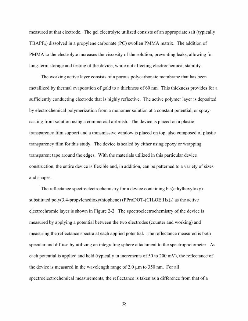
reflectance occurs 400 mV before any change in the visible region reflectance occurs in the
device, exhibiting unsymmetrical switching.
Figure 2-4. Percent reflectance versus cell potential (A) for a 450 nm thick PProDOT-
(CH2OEtHx)2 film reflective ECD. Transmittance versus potential (B) for a film of the same polymer and thickness on ITO-glass in 0.2 M TBAPF6/PC electrolyte.
On the other hand, for that same polymer thickness, the NIR and visible region
transmittance change occurs at the same potential, as is seen in Figure 2-4B, not exhibiting any
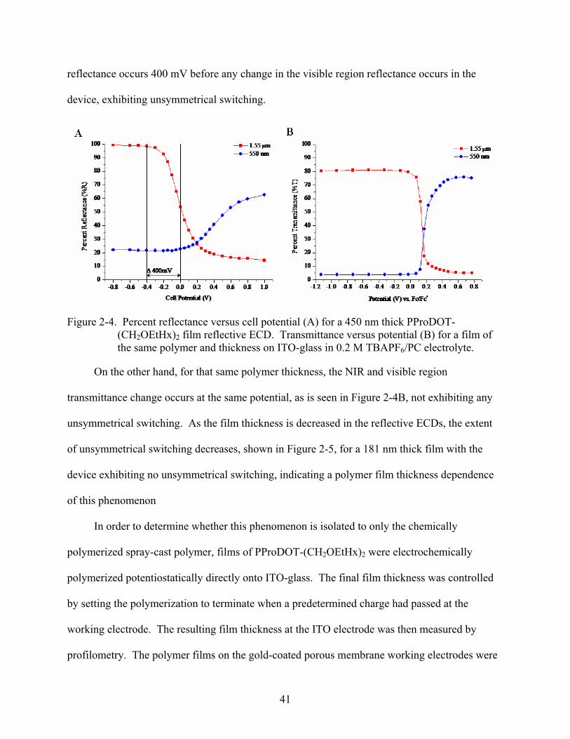
unsymmetrical switching. As the film thickness is decreased in the reflective ECDs, the extent
of unsymmetrical switching decreases, shown in Figure 2-5, for a 181 nm thick film with the
device exhibiting no unsymmetrical switching, indicating a polymer film thickness dependence
of this phenomenon
In order to determine whether this phenomenon is isolated to only the chemically
polymerized spray-cast polymer, films of PProDOT-(CH2OEtHx)2 were electrochemically
polymerized potentiostatically directly onto ITO-glass. The final film thickness was controlled
by setting the polymerization to terminate when a predetermined charge had passed at the
working electrode. The resulting film thickness at the ITO electrode was then measured by
profilometry. The polymer films on the gold-coated porous membrane working electrodes were
42
obtained by the same method. Given that the thickness of the polymer films on the gold-coated
porous membranes could not be measured by profilometry, it was assumed that the thickness
produced on the membrane was similar to that on ITO with the charge passed for polymerization
corrected for the electrode area differences.
Figure 2-5. Percent reflectance versus cell potential for a 181 nm thick PProDOT-(CH2OEtHx)2
film reflective ECD demonstrating the lack of unsymmetrical switching in the thinner films.
The reflectance spectroelectrochemical series for a polymer film 998 nm thick in an ECD
is shown in Figure 2-6A and that of the same film thickness measured by transmittance on ITO-
glass is shown in Figure 2-6B. The NIR reflectance begins to decrease at -0.4 V while the
visible region reflectance begins to increase at +0.1 V, 500 mV later for the polymer film in the
reflectance device. On the other hand, the NIR transmittance decreases at the same applied
potential for the polymer film on ITO-glass. This can be more clearly see in Figure 2-7 where
the percent reflectance versus cell potential for the three different film thicknesses (111, 538, and
998 nm) of electropolymerized polymer are shown. Similarly, with the spray-cast films, this

43
extent of unsymmetrical switching in the reflective ECDs shows a film thickness dependence on
the electrochemically polymerized films.
Figure 2-6. Reflectance spectroelectrochemistry (A) for a 998 nm thick electropolymerized
PProDOT-(CH2OEtHx)2 film in an ECD. Transmittance spectroelectrochemistry (B) for a film of the same thickness on ITO-glass in 0.2 M TBAPF6/PC with potentials referenced versus Fc/Fc+
Figure 2-7. Percent reflectance versus cell potential for reflective ECDs of electrochemically
polymerized PProDOT-(CH2OEtHx)2 of thickness A) 111 nm, B) 538 nm, and C) 998 nm.
A comparison was made between films on ITO-glass and in reflective ECDs of two
different spray-cast polymers, PProDOT-(CH2OEtHx)2 and PProDOT-Hx2. Initial experiments
where the unsymmetrical switching was evident were performed on devices containing the
alkoxy branched polymer, PProDOT-(CH2OEtHx)2. The linear alkyl derivative was then
investigated for the presence of unsymmetrical switching when incorporated in reflective devices

44
to determine whether this phenomenon is isolated to one specific polymer or is present in the
family of disubstituted PProDOTs.
As Figure 2-8 shows, unsymmetrical switching is found to occur in the linear alkyl
derivative as well when incorporated into reflective ECDs, but not when measured by
transmittance on ITO-glass. This indicates that the phenomenon is not due to the branched
alkoxy groups on the polymers, but rather to the large optical contrasts in the NIR and the
relative ease with which to prepare thick films, both spray-cast and electrochemically
polymerized, for this family of polymers.
Figure 2-8. Percent reflectance versus cell potential(A) for a 351 nm spray-cast film of
PProDOT-Hx2 in a reflective ECD. Percent transmittance (B) versus potential for a film of the same thickness on ITO-glass in 0.2 M TBAPF6/PC. Potentials are referenced vs. Fc/Fc+.
Conductive Front
Here, a model is proposed for the effect of unsymmetrical switching in reflective ECDs of
conjugated conducting polymers. As was discussed previously in Chapter 1, a conjugated
conducting polymer is insulating in its neutral, undoped state. Other researchers have shown that
there is a process whereby the neutral polymer film is oxidized electrochemically in a localized

45
area beginning at the electrode/polymer interface.137-143 This oxidized area is now conductive
and acts as an extension of the metallic electrode to further oxidize to conductive domains farther
from the electrode surface. This process continues until the conductive zone, or front, reaches
the polymer film surface and is shown schematically in Figure 2-9.
When the film is neutral and insulating, the polymer is highly absorptive in the visible
region and highly transmissive in the NIR. As can be seen in the spectra in Figure 2-9A, a large
amount of light in the visible region is absorbed (~90% at λmax) and therefore only a small
amount is able to traverse the entire film and be reflected back by the gold electrode. On the
other hand, ~90% of the light in the wavelength range of 800 to 2000 nm is measured, indicating
that nearly all the light is able to penetrate through the entire film, be reflected by the electrode
and travel through the film a second time to be measured.
At low applied potentials, the film becomes oxidized to a small distance from the
polymer/electrode interface. The concentration of conductive sites is low and the redox-doped
front does not penetrate far into the insulating film as shown in Figure 2-9B. Given that the NIR
light is able to penetrate the entire polymer film, this small increase in the concentration of
oxidized species at the polymer/electrode interface is able to be probed at those wavelengths and
a change in the spectra is observed. However, nearly all of the visible region light is absorbed by
the polymer film before reaching the conductive front and no change in the redox state of the
polymer is measured by this wavelength range. This can be seen in the reflectance spectra where
an absorbance change is seen in the wavelength range of 700 to 2000 nm with no change in the
visible region below 700 nm. As the doping level increases at higher applied potentials, the
concentration of oxidized sites increases and the conductive front propagates farther into the
polymer film, as shown in Figure 2-9C.

46
Figure 2-9. Conductive front model. A) Schematic of fully neutralized film showing penetration
of visible (blue line) and NIR (red line) and respective spectra. Width and dashing of lines indicate intensity of light. B) Conductive front propagating through film at low applied potentials. C) Conductive front propagating further into film at higher applied potentials, past the penetration depth of visible light. D) Fully oxidized film.

47
An even higher concentration of oxidized species is probed by the NIR light and, since the
conductive front has now extended past the penetration depth of the visible light, there is now a
measure of the oxidized portion of the film by this wavelength range as shown with a change in
the visible region absorbance. The NIR absorbance is constantly increasing as the concentration
of doped polymer is increasing, but the measurement of optical change in the visible region
cannot occur until the conductive front extends past the penetration limit of visible light. Once
the entire film becomes fully oxidized, as is shown in Figure 2-9D, the polymer is highly
absorbing in the NIR and highly transmissive in the visible region, with the visible light now
able to penetrate through the entire film to the exposed gold electrode underneath.
The distance to which light can penetrate a material can be determined from the
penetration depth, δ, also known as the skin depth. This depth is dependent on the absorption
coefficient of the sample and is defined as the depth at which the intensity of radiation inside the
material falls to 1/e of the original value at the material surface and is calculated by:
δ = 2/α (2-1)
where α is the absorption coefficient and can be determined from the transmission through the
sample of known thickness as shown schematically in Figure 2-10. To determine this value for
the entire wavelength range, polymer films of several different thicknesses were deposited on
glass and the transmittance through the polymer film from the wavelength range of 350 nm to
2000 nm were measured. These films can be treated as planar layered structures from which the
optical transmission can be determined while taking internal reflections into considerations. For
the case of an absorbing layer (polymer film) on a nonabsorbing substrate (glass), the relation
between optical transmission and absorption coefficient has previously been determined144 and is
as follows:

48
T=1 - R12R23 - A
2R01(R12 + R23 - 2R12R23)
(1 - R01) (1 - R12) (1 - R23)A
(2-2)
and the value of A is defined as A = e-αt (where t is the thickness of the absorbing polymer layer),
and Rjk is the layer-layer power reflection coefficient for each layer noted in Figure 2-10.
Figure 2-10. Schematic of multilayer geometry used in analysis of penetration depth of optical
radiation through the polymer sample. Material 1 is the absorbing polymer film, material 2 is the nonabsorbing glass substrate. The reflections at each surface are indicated by Rjk.
Given that the reflections at each surface are much less than 1, the denominator in equation
2-2 reduces to 1 and the transmission then becomes:
T=(1 - R01) (1 - R12) (1 - R23)e-at
(2-3)
If the ratio of the transmission,T, for samples of two different thicknesses (A and B) are taken,
the equation reduces further to:
TATB = e-atA
e-atB=e-a(tB - tA)
(2-4)
The penetration depth, δ, is now calculated by:
49
d=a2=
lnTB - lnTA
-2(tB - tA)
(2-5)
The penetration depth for spray-cast films of PProDOT-(CH2OEtHx)2 were determined by
measuring the transmittance of samples of various thicknesses (specifically 93, 133, and 189 nm)
over the wavelength range of 350 nm to 2000 nm and calculating the penetration depth from
equation 2-5. The average penetration depth at 1.55 µm was calculated to be 15 µm and that at
550 nm (the λmax for this polymer) was calculated to be 0.35 µm. Therefore, film thicknesses of
this polymer of 0.15 µm or less should exhibit no unsymmetrical switching when incorporated
into reflective ECDs as the light in the visible region is able to travel through the entire polymer
film, be reflected off the gold electrode and travel back to be measured. In films thicker than
0.35 µm, the penetration depth is not far enough for the light to reach the polymer/electrode
interface to measure any optical changes that occur close to the electrode at low oxidation
potentials, which is the case as was shown in Figure 2-7 for three different film thicknesses of
PProDOT-(CH2OEtHx)2 in reflective ECDs.
This phenomenon of unsymmetrical switching exhibited by these devices has possible
applications with one being variable thermal control. It can be imagined a reflective device that,
when in the fully reduced state, allows for all NIR light to be fully reflected while the device is
colored. By adjusting the device bias, it remains in that colored state in the visible region, but
the NIR light is absorbed and can be collected and transferred using a heat conducting element.
Another possible application for this feature is the utilization of this device in combination with a
solar cell placed such that light is reflected off the ECD before being directed to the solar cell.
The amount of light in the near to mid IR impinging on a photovoltaic device can be tuned while
excluding light from the visible region. In effect, the device would act as a tunable filter for the

50
solar cell. Yet another possible application is in the area of optical telecommunications and will
be discussed in the next section.
Reflective ECDs as Variable Optical Attenuators
A device that can take advantage of the large, tunable NIR contrasts exhibited with
conjugated polymer ECDs is the variable optical attenuator (VOA). VOAs are key components
in fiber-optic telecommunications networks and are utilized to reduce signal power by inducing a
fixed or variable loss.145, 146 VOAs are also often required in applications where photosensitive
components require dissimilar incident optical signals, and hence variable sensitivities and
saturation points. The attenuator regulates the light intensity to be within the dynamic range of
the component, preventing any damage or overloading.
In recent years, the use of wavelength division multiplexing (WDM) has become important
to handle the increased demand placed on optical telecommunications by fiber-optic
transmission.147, 148 With WDM, a number of signals of differing wavelengths are combined
onto a single fiber allowing for increased signal density without increasing the amount of optical
fiber used. These systems require that the optical power between all channels be equalized
before combination. Direct control of the source for each signal is not practical as changes in the
laser drive current can lead to an undesirable wavelength shift. VOAs allow for adjustment of
the channel power while maintaining wavelength stability.
Another application of VOAs is for channel balancing to optimize the optical power of
signals at key points in the networks. Optical power levels are determined by the optical loss
along the transmission line and can vary with the length of the line, the number of connection
points, and the efficiency of optical components (e.g., couplers, amplifiers, and source) and
deterioration of the signal-to-noise ratio may reduce the optical transmission quality. A VOA is

51
capable of maintaining the light level acting as a noise discriminator, reducing the intensity of
spurious signals to below a threshold value.
Additionally, VOAs serve to control feedback in optical amplifier control loops to
maintain a constant output (e.g., as an automatic gain control element (AGC)). In WDM
systems, transmission loss is compensated by utilizing erbium-doped amplifiers (EDFAs), which
amplify the signal made up of numerous wavelengths. However, EDFA gain is wavelength-
dependent and a gain equalizer is needed that has a wavelength dependence profile that is the
inverse of the EDFA in order to maintain a flat transmission bandwidth. However, when there is
a change in the optical power to the EDFA, the wavelength dependence of the EDFA gain profile
changes. Since the profile of the gain equalizer is fixed, there is a shift in the flattening effect
that it provides. The VOA allows for tuning of the signal to compensate for this gain tilt and
flattens the transmission profile.
When considering the optical performance of a VOA, the most important specifications are
insertion loss and range of optical attenuation. These values are typically reported for the most
commonly used wavelengths, 1.55 and 1.31 µm as these are the wavelengths where absorption
and dispersion are the lowest for silica fibers. The range of optical attenuation is the minimum
and maximum attenuation values achievable by the device with optical attenuation measured by:
Optical Attenuation (dB) = 10 log10 (Ioff/Ion) (2.6)
where Ioff and Ion are the intensity of the signal when the attenuator is in the “off” state and “on”
state, respectively. Many VOAs either transmit or reflect light so intensity is the percent
reflected or transmitted by the attenuator. For a variable optical attenuator, the on state can be
tuned as a function of voltage applied to the device yielding a dynamic attenuation range.
Typical VOA attenuation values range from 10 to 25 dB with many VOAs able to achieve up to

52
50 dB attenuation. To illustrate the significance of such values, a 3 dB loss leaves 50% of the
original light signal, a 10 dB loss leaves 10%, and a 20 dB loss leaves 1%.
Ideally, when the attenuator is in the off state, the amount of light transmitted or reflected
would be 100%, very often this is not the case. The insertion loss (or optical loss) is the amount
of light lost when the attenuator is off and is calculated by:
Optical Loss (dB) = 10 log10(100%/Ioff) (2.7)
where again, Ioff is the intensity of the optical signal when the attenuator is off and is commonly
expressed as percent transmittance or percent reflectance. Optical loss in a fiber-optic system is
additive, therefore the loss due to the introduction of a VOA into the network is needed to be
kept to a minimum. Given that the loss due to fiber attenuation alone can be as low as 1 dB/km,
for many applications, the maximum insertion loss tolerated is less than 1 dB.
Optical attenuation and insertion loss values vary with the type of attenuator device
utilized with there being a large number of devices that are either commercially available or
currently researched. Many of these devices differ in their operating mechanism, which also
determines other performance characteristics such as drive voltage, switching speed, and size.
The most common VOAs being developed are those that include liquid crystal devices,
mechanical actuators, microelectromechanical (MEMs) devices, and electrochromic devices.
The liquid crystal devices operate by passing the light through a liquid crystal element.149,
150 When a voltage is applied to the device the liquid crystal molecules are oriented in such a
way that light is attenuated. These devices allow for efficient tunable attenuation; however,
liquid crystals are temperature sensitive and as the temperature of the surrounding environment
varies, the optical properties of the liquid crystal change, resulting in higher insertion loss and
inaccurate attenuation.
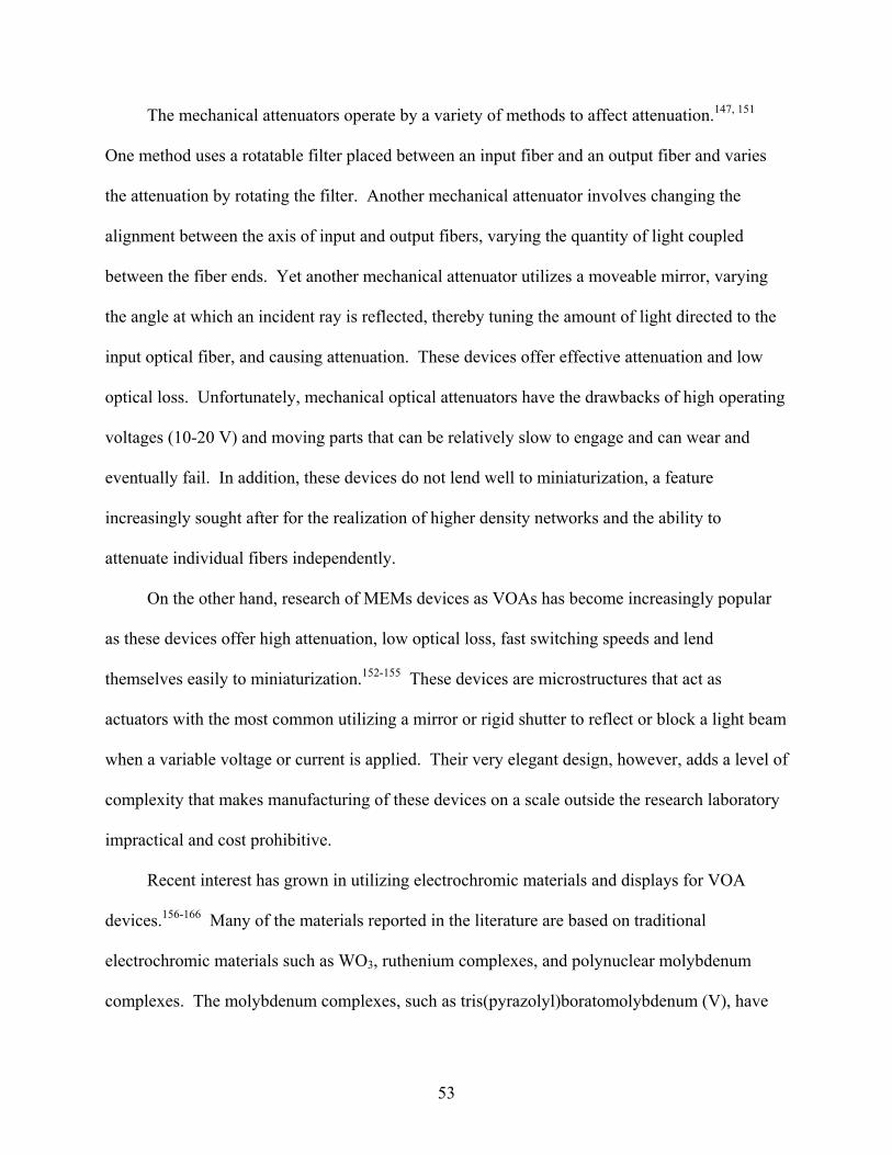
53
The mechanical attenuators operate by a variety of methods to affect attenuation.147, 151
One method uses a rotatable filter placed between an input fiber and an output fiber and varies
the attenuation by rotating the filter. Another mechanical attenuator involves changing the
alignment between the axis of input and output fibers, varying the quantity of light coupled
between the fiber ends. Yet another mechanical attenuator utilizes a moveable mirror, varying
the angle at which an incident ray is reflected, thereby tuning the amount of light directed to the
input optical fiber, and causing attenuation. These devices offer effective attenuation and low
optical loss. Unfortunately, mechanical optical attenuators have the drawbacks of high operating
voltages (10-20 V) and moving parts that can be relatively slow to engage and can wear and
eventually fail. In addition, these devices do not lend well to miniaturization, a feature
increasingly sought after for the realization of higher density networks and the ability to
attenuate individual fibers independently.
On the other hand, research of MEMs devices as VOAs has become increasingly popular
as these devices offer high attenuation, low optical loss, fast switching speeds and lend
themselves easily to miniaturization.152-155 These devices are microstructures that act as
actuators with the most common utilizing a mirror or rigid shutter to reflect or block a light beam
when a variable voltage or current is applied. Their very elegant design, however, adds a level of
complexity that makes manufacturing of these devices on a scale outside the research laboratory
impractical and cost prohibitive.
Recent interest has grown in utilizing electrochromic materials and displays for VOA
devices.156-166 Many of the materials reported in the literature are based on traditional
electrochromic materials such as WO3, ruthenium complexes, and polynuclear molybdenum
complexes. The molybdenum complexes, such as tris(pyrazolyl)boratomolybdenum (V), have

54
been reported to have the highest attenuation out of these with a value of 50 dB at a low applied
voltage.156, 159, 165 However, the prototype devices are based on a solution of the electrochrome
sandwiched between two transparent electrodes. This limits the device architecture , and
switching speed, as the species is required to diffuse to the electrode to be redox switched. The
transition metal oxide film devices based on WO3 have also shown impressive attenuation of 40
dB, reaching 20 dB in 2 seconds, but require an hour for the device to return to the transmissive
state.158, 164 Dendritic mixed-valence ruthenium complexes have also been researched as VOA
materials with films showing attenuation values of 2-7 dB, switching within 2 seconds.160-162
The first reported use of a conjugated polymer as a possible electrochromic VOA material
were for films of PEDOT.163, 167 These devices were shown to have an optical attenuation of 11
dB, switching within 5-7 seconds and a low optical loss of 0.86 dB. Conjugated electrochromic
polymers and their devices offer many advantages not available with the other devices and
materials discussed. These include a low operating voltage (under ± 1.5 V), mechanical
flexibility, improved film processability, and a variety of options in device design and patterning.
It is demonstrated in this chapter the applicability of the previously introduced reflective
electrochromic displays, with PProDOT-(CH2OEtHx)2 as the active layer, as an electrochromic
variable optical attenuator (EC-VOA).
The reflective ECD was constructed as previously described in this chapter. Briefly, the
counter electrode consisted of PEDOT electrochemically deposited onto a gold-coated Kapton®
electrode. The next layer was comprised of porous filter papers soaked with a
TBAPF6/PMMA/PC gel electrolyte. This was followed by the outward-facing working electrode
that was a gold-coated porous polycarbonate membrane onto which the active polymer layer
(PProDOT-(CH2OEtHx)2) was spray-cast. The entire device was encapsulated with a plastic

55
transparency film back support and cover, and sealed on all four sides with transparent tape.
Initial measurements were performed with a UV/Vis-NIR spectrophotometer fitted with an
integrating sphere as described in Chapter 5. The percent reflectance of the device was measured
for each potential applied and optical attenuation and insertion loss values were calculated using
equations 2-6 and 2-7.
As is shown in Figure 2-11, for a 750 nm thick film, the maximum attenuation achieved
was 11.2 dB at an applied voltage of 400 mV for the wavelength of 1.55 µm and 10.6 dB at 700
mV for 1.31 µm. The optical loss when this device was fully reduced was low with a value of
0.1 dB at 1.55 µm and 0.2 dB at 1.31 µm.
Figure 2-11. Optical attenuation at various applied potentials for a 750 nm thick film of
PProDOT-(CH2OEtHx)2 in a reflective ECD as an EC-VOA at the wavelengths of 550, 1310, and 1550 nm.
To further demonstrate the possibility of this device as an EC-VOA, a model fiber-optic
setup was fabricated as shown schematically in Figure 2-12A and in the photograph in Figure 2-
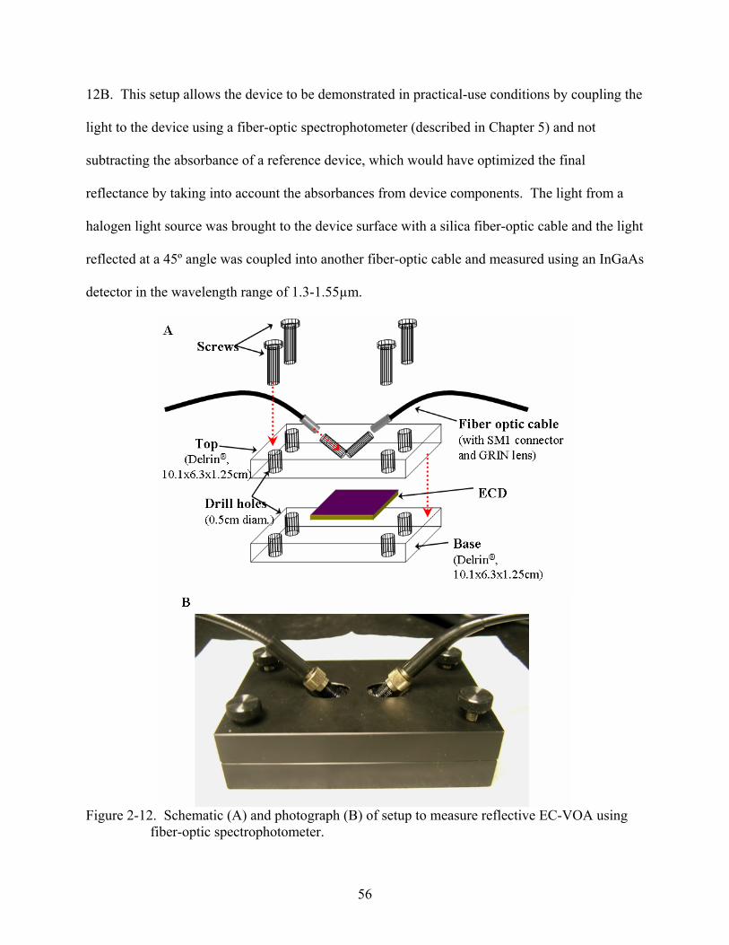
56
12B. This setup allows the device to be demonstrated in practical-use conditions by coupling the
light to the device using a fiber-optic spectrophotometer (described in Chapter 5) and not
subtracting the absorbance of a reference device, which would have optimized the final
reflectance by taking into account the absorbances from device components. The light from a
halogen light source was brought to the device surface with a silica fiber-optic cable and the light
reflected at a 45º angle was coupled into another fiber-optic cable and measured using an InGaAs
detector in the wavelength range of 1.3-1.55µm.
Figure 2-12. Schematic (A) and photograph (B) of setup to measure reflective EC-VOA using
fiber-optic spectrophotometer.
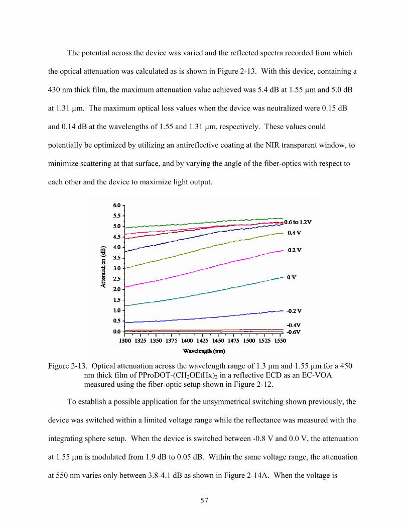
57
The potential across the device was varied and the reflected spectra recorded from which
the optical attenuation was calculated as is shown in Figure 2-13. With this device, containing a
430 nm thick film, the maximum attenuation value achieved was 5.4 dB at 1.55 µm and 5.0 dB
at 1.31 µm. The maximum optical loss values when the device was neutralized were 0.15 dB
and 0.14 dB at the wavelengths of 1.55 and 1.31 µm, respectively. These values could
potentially be optimized by utilizing an antireflective coating at the NIR transparent window, to
minimize scattering at that surface, and by varying the angle of the fiber-optics with respect to
each other and the device to maximize light output.
Figure 2-13. Optical attenuation across the wavelength range of 1.3 µm and 1.55 µm for a 450
nm thick film of PProDOT-(CH2OEtHx)2 in a reflective ECD as an EC-VOA measured using the fiber-optic setup shown in Figure 2-12.
To establish a possible application for the unsymmetrical switching shown previously, the
device was switched within a limited voltage range while the reflectance was measured with the
integrating sphere setup. When the device is switched between -0.8 V and 0.0 V, the attenuation
at 1.55 µm is modulated from 1.9 dB to 0.05 dB. Within the same voltage range, the attenuation
at 550 nm varies only between 3.8-4.1 dB as shown in Figure 2-14A. When the voltage is
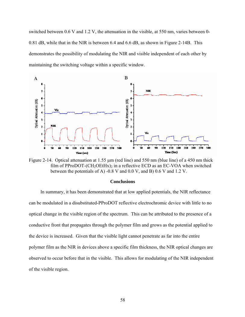
58
switched between 0.6 V and 1.2 V, the attenuation in the visible, at 550 nm, varies between 0-
0.81 dB, while that in the NIR is between 6.4 and 6.6 dB, as shown in Figure 2-14B. This
demonstrates the possibility of modulating the NIR and visible independent of each other by
maintaining the switching voltage within a specific window.
Figure 2-14. Optical attenuation at 1.55 µm (red line) and 550 nm (blue line) of a 450 nm thick
film of PProDOT-(CH2OEtHx)2 in a reflective ECD as an EC-VOA when switched between the potentials of A) -0.8 V and 0.0 V, and B) 0.6 V and 1.2 V.
Conclusions
In summary, it has been demonstrated that at low applied potentials, the NIR reflectance
can be modulated in a disubstituted-PProDOT reflective electrochromic device with little to no
optical change in the visible region of the spectrum. This can be attributed to the presence of a
conductive front that propagates through the polymer film and grows as the potential applied to
the device is increased. Given that the visible light cannot penetrate as far into the entire
polymer film as the NIR in devices above a specific film thickness, the NIR optical changes are
observed to occur before that in the visible. This allows for modulating of the NIR independent
of the visible region.

59
In addition, reflective ECDs containing sprayable PProDOTs have been demonstrated as
electrochromic variable optical attenuators. Not only do these devices offer effective optical
attenuation and low insertion loss, but also the advantage of mechanical flexibility, low drive
voltage and the possibility of patterning for the fabrication of multiple, individually addressable
devices in a variety of architectures. Future directions for these devices as VOAs would include
optimization of the device performance. This would entail determining the optimum polymer
film thickness for the highest attenuation while maintaining a low insertion loss. Additionally,
coupling the fiber-optics to the device in such a way as to achieve the maximum reflectance of
incident light measured. The possibilities for achieving this would include a fiber-optic holder
with adjustable incident and outcoupling angles. The current fiber-optic holder is constructed
such that the light measured is at a 45 degree angle to the incident light, however, this may not
be the optimum angle for the measurement of reflectance from the devices. Further work could
also include patterning of the devices to form individually addressable pixels each containing a
separate, miniature, EC-VOA.

60
CHAPTER 3 ELECTROCHROMIC DISPLAYS OF MEH-PPV AND CARBAZOLE-CONTAINING
COPOLYMERS
All conjugated electroactive polymers are potentially electrochromic with many polymers
exhibiting multiple colored states.22 As was introduced in Chapter 1, the color of the polymer
neutral state is determined by the polymer bandgap. Some of the most highly researched
electrochromic polymers are those based on the alkylenedioxy-bridged thiophenes and pyrroles.
The alkylenedioxythiophenes are low bandgap polymers with a π-π* transition in the visible
region making them cathodically coloring, switching from a highly absorptive to a highly
transmissive state on oxidation. The presence of electron-donating oxygens adjacent to the
thiophene ring acts to raise the HOMO level, lowering the polymer oxidation potential relative to
the unsubstituted thiophene polymer. For example, the onset of oxidation for the dioxythiophene
polymers, PEDOT and PProDOT-(CH2OEtHx)2 are -0.2 V and 0.2 V vs. SCE, respectively.48, 168,
169 This allows these polymers to be more stable in the oxidized form under ambient conditions
as their HOMO levels are above the threshold for air stability, which is defined by the O2 to H2O
redox couple at 0.5 V vs. SCE, shown in Figure 3-1, as they are easily oxidized by molecular
oxygen.170 On the other hand, polymers with HOMO levels lower than 0.5 V vs. SCE, such as
MEH-PPV and PFO, are stable in their neutral form under ambient conditions yet become more
difficult to electrochemically switch as the oxidation potential increases.169, 171
Similarly, the addition of an alkylenedioxy bridge to pyrrole introduces electron density to
the already electron-rich pyrrole unit, acting to further lower the polymer oxidation potential to
the lowest values reported for conjugated polymers.22, 50, 54 By substitution at the nitrogen of the
pyrrole ring, a reduction in the effective conjugation length can be induced by the steric
interactions brought about by torsional twisting and the polymer bandgap can be increased to
values greater than 3.0 eV, shifting the neutral polymer absorbance into the UV region.52 By

61
increasing the polymer bandgap, the HOMO level is lowered. However, the N-substituted
PProDOPs still maintain a low oxidation potential allowing these polymers to have the lowest
values for anodically coloring polymers to date. As with the dioxythiophenes, the family of
PProDOPs are highly stable in the oxidized state.
Figure 3-1. Diagram of oxidation potentials (vs. SCE) for several electrochromic and
electroluminescent polymers relative to the level required for air stability along with optical bandgap values.48, 52, 168, 169, 171
While high HOMO values allow for a low oxidation potential and a stable p-doped state,
characteristics desirable in electrochromic applications, this is not the case for light-emitting
display applications. For effective hole injection to occur, the polymer HOMO level must be
located at levels close to the work function of the anode. The most commonly utilized anode
material is ITO with a work function of 4.8 eV or PEDOT:PSS-modified ITO with a work
function of 5.2 eV.85, 172, 173 In addition, as the polymer active layer utilized in PLEDs is in the
pristine, neutral form and the presence of any doped sites quenches luminescence, it is necessary
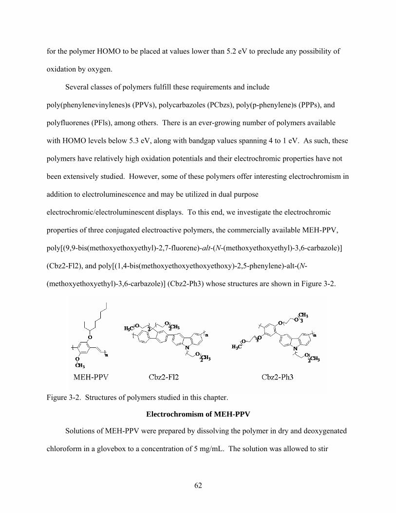
62
for the polymer HOMO to be placed at values lower than 5.2 eV to preclude any possibility of
oxidation by oxygen.
Several classes of polymers fulfill these requirements and include
poly(phenylenevinylenes)s (PPVs), polycarbazoles (PCbzs), poly(p-phenylene)s (PPPs), and
polyfluorenes (PFls), among others. There is an ever-growing number of polymers available
with HOMO levels below 5.3 eV, along with bandgap values spanning 4 to 1 eV. As such, these
polymers have relatively high oxidation potentials and their electrochromic properties have not
been extensively studied. However, some of these polymers offer interesting electrochromism in
addition to electroluminescence and may be utilized in dual purpose
electrochromic/electroluminescent displays. To this end, we investigate the electrochromic
properties of three conjugated electroactive polymers, the commercially available MEH-PPV,
poly[(9,9-bis(methoxyethoxyethyl)-2,7-fluorene)-alt-(N-(methoxyethoxyethyl)-3,6-carbazole)]
(Cbz2-Fl2), and poly[(1,4-bis(methoxyethoxyethoxyethoxy)-2,5-phenylene)-alt-(N-
(methoxyethoxyethyl)-3,6-carbazole)] (Cbz2-Ph3) whose structures are shown in Figure 3-2.
Figure 3-2. Structures of polymers studied in this chapter.
Electrochromism of MEH-PPV
Solutions of MEH-PPV were prepared by dissolving the polymer in dry and deoxygenated
chloroform in a glovebox to a concentration of 5 mg/mL. The solution was allowed to stir
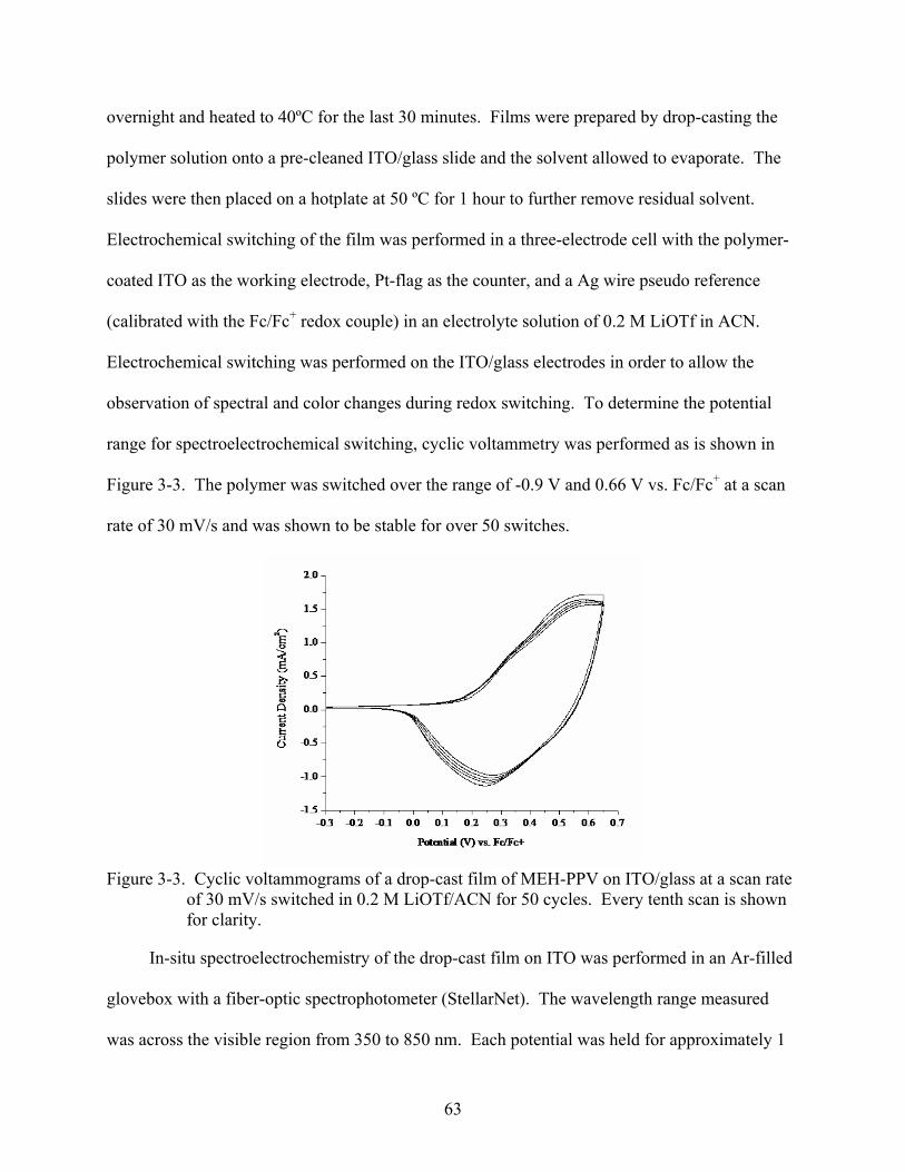
63
overnight and heated to 40ºC for the last 30 minutes. Films were prepared by drop-casting the
polymer solution onto a pre-cleaned ITO/glass slide and the solvent allowed to evaporate. The
slides were then placed on a hotplate at 50 ºC for 1 hour to further remove residual solvent.
Electrochemical switching of the film was performed in a three-electrode cell with the polymer-
coated ITO as the working electrode, Pt-flag as the counter, and a Ag wire pseudo reference
(calibrated with the Fc/Fc+ redox couple) in an electrolyte solution of 0.2 M LiOTf in ACN.
Electrochemical switching was performed on the ITO/glass electrodes in order to allow the
observation of spectral and color changes during redox switching. To determine the potential
range for spectroelectrochemical switching, cyclic voltammetry was performed as is shown in
Figure 3-3. The polymer was switched over the range of -0.9 V and 0.66 V vs. Fc/Fc+ at a scan
rate of 30 mV/s and was shown to be stable for over 50 switches.
Figure 3-3. Cyclic voltammograms of a drop-cast film of MEH-PPV on ITO/glass at a scan rate
of 30 mV/s switched in 0.2 M LiOTf/ACN for 50 cycles. Every tenth scan is shown for clarity.
In-situ spectroelectrochemistry of the drop-cast film on ITO was performed in an Ar-filled
glovebox with a fiber-optic spectrophotometer (StellarNet). The wavelength range measured
was across the visible region from 350 to 850 nm. Each potential was held for approximately 1

64
minute before the spectra was acquired as this was the length of time required for optical changes
to equilibrate. Figure 3-4A shows the spectra of the as-cast, dry film and the
spectroelectrochemistry of the film at low (-0.94 to 0.36 V) applied potentials. The
spectroelectrochemistry for higher potentials is shown in Figure 3-4B for clarity. As seen in
Figure 3-4A, the neutral, as-cast, film shows a λmax of 483 nm with an absorption onset of 562
nm, giving an optical bandgap value of 2.2 eV. The λmax is blue-shifted by 36 nm from the
neutralized film (-0.94 V) as the as-cast spectra was taken on a dry film. This is because the
electrochemically switched film is electronically different from the as-cast film due to
electrochemical annealing of the film inducing both a shift in the absorbance to longer
wavelengths and broadens the spectra.
Figure 3-4. Spectroelectrochemistry (A) of a drop-cast film of MEH-PPV on ITO/glass switched
in 0.2 M LiOTf/ACN. The arrow shows direction of spectral growth. Photographs (B) of the same film held at potentials indicated. All potentials given are referenced vs. Fc/Fc+.
65
When a potential sufficiently positive enough (+0.31 V) to cause oxidation of the polymer
is applied to the film the absorbance at the λmax decreases while a broad absorbance beginning at
600 nm begins to increase. This is due to the introduction of lower energy midgap state and
depletion of the valence band as discussed in Chapter 1. A further increase in the potential
applied to the film (+0.36 V) causes a shift in the λmax to shorter wavelengths and a further
increase in the long wavelength absorbance. The shift in the λmax is due to the widening of the
bandgap. This is because as the polymer is oxidized, electrons are removed from the top of the
valence band and the now the minimum energy required for the electronic transition from the
HOMO to the LUMO is higher. On further oxidation, the absorbance at λmax continues to
decrease and shift to shorter wavelengths while the longer wavelength absorbances from 600 to
800 nm also decrease as shown in Figure 3-4B. The polymer goes through several colored states
on oxidation as is seen in the photographs in Figure 3-4C. It should be noted that the unevenness
in the films, as seen in the photographs, is due to the uneven evaporation of the solvent from the
electrode edges during drop-casting. The fully reduced polymer is an orange-red color at -0.9 V
and blue at +0.66 V vs. Fc/Fc+ with colored states of brown and greenish-blue at intermediate
potentials.
Electrochromism of Cbz2-Fl2
Solutions of the carbazole-fluorene copolymer were made by dissolving the polymer in dry
and deoxygenated chloroform to a concentration of 5 mg/mL. Films were cast onto ITO/glass
electrodes by spray-casting from a commercial airbrush (Testor Corp., Rockford, IL) operated at
a pressure of 20 psi. The films were then dried at 50ºC in a vacuum oven for 1 hour. As this
polymer is soluble in many electrochemical solvents (i.e., chloroform, ACN, propylene
carbonate, methylene chloride) except water, electrochemical switching was performed in an
electrolyte of 0.2 M LiOTf in water. This, however, precluded electrochemical and

66
spectroelectrochemical characterization in the glovebox and all experiments were performed on
the bench after purging the electrolyte with Argon for at least 20 minutes. As with the MEH-
PPV films, the accessible electrochemical window for in-situ spectroelectrochemistry was
determined by switching the polymer film on ITO by CV. While distinct color changes could be
seen and an increase in current attributed to the polymer oxidation occurred, there was no
discernable redox peak found on cycling to allow for determination of a polymer E1/2 as can be
seen in Figure 3-5. The peak oxidation of the polymer occurs roughly at the same potential as
the electrolyte oxidation, which is shown by the dashed line. This oxidation of the supporting
electrolyte interfered with the polymer oxidation, not allowing for switching at higher potentials
to observe a peak current. Therefore, polymer oxidation was determined as the onset of anodic
current increase.
Figure 3-5. Cyclic voltammograms of a spray-cast film of Cbz2-Fl3 on ITO/glass switched at 30
mV/s in 0.2 M LiOTf/water for 50 scans. Every tenth scan is shown for clarity. The background scan (0.2 M LiOTf/water) is shown by the dashed line.
Film in situ spectroelectrochemistry was performed with a Cary 500 UV/Vis-NIR
spectrophotometer by holding the potential applied to the film for one minute and recording the
spectra from 350 to 800 nm. The one minute hold time was determined as with MEH-PPV by

67
monitoring the spectra until it no longer fluctuated. The λmax of the neutral film was determined
by casting the polymer onto a quartz slide as the absorbance extends into the UV and could not
accurately be determined on ITO/glass. The absorbance of the neutral, dry film is shown in
Figure 3-6A by the dashed line. The λmax is 349 nm with an absorption onset of 310 nm giving
an optical bandgap of 3.0 eV.
Figure 3-6. Spectroelectrochemistry (A and B) of a spray-cast film of Cbz2-Fl2 on ITO/glass in
0.2 M LiOTf/water. The arrow shows direction of spectral growth and recession. Photographs (C) of the same film held at various potentials. All potentials given are referenced versus Fc/Fc+.
As with MEH-PPV, the absorbance spectra of the electrolyte-soaked film is red-shifted (by
13 nm) due to swelling of the film. The spectroelectrochemical series shows a slight decrease in
absorbance at 350 nm on oxidation while an increase in absorbance at 500 nm and a broad
absorbance extending from the NIR as can be seen in Figure 3-6A. The absorbances began to
decrease beginning at the applied potential of 0.56 V as shown in Figure 3-6B. The polymer was
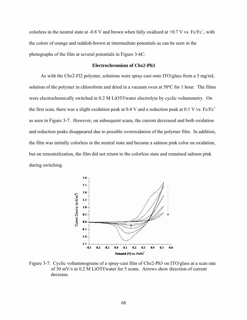
68
colorless in the neutral state at -0.8 V and brown when fully oxidized at +0.7 V vs. Fc/Fc+, with
the colors of orange and reddish-brown at intermediate potentials as can be seen in the
photographs of the film at several potentials in Figure 3-6C.
Electrochromism of Cbz2-Ph3
As with the Cbz2-Fl2 polymer, solutions were spray-cast onto ITO/glass from a 5 mg/mL
solution of the polymer in chloroform and dried in a vacuum oven at 50ºC for 1 hour. The films
were electrochemically switched in 0.2 M LiOTf/water electrolyte by cyclic voltammetry. On
the first scan, there was a slight oxidation peak at 0.4 V and a reduction peak at 0.1 V vs. Fc/Fc+
as seen in Figure 3-7. However, on subsequent scans, the current decreased and both oxidation
and reduction peaks disappeared due to possible overoxidation of the polymer film. In addition,
the film was initially colorless in the neutral state and became a salmon pink color on oxidation,
but on reneutralization, the film did not return to the colorless state and remained salmon pink
during switching.
Figure 3-7. Cyclic voltammograms of a spray-cast film of Cbz2-Ph3 on ITO/glass at a scan rate
of 30 mV/s in 0.2 M LiOTf/water for 5 scans. Arrows show direction of current decrease.

69
As this polymer is not stable to repeated switching, a fresh film was cast for
spectroelectrochemical measurements without breaking-in the film by switching before
measuring the spectra. Similarly with the Cbz2-Fl2 polymer, the λmax of the neutral film
occurred in the UV, as can be seen in Figure 3-8A for the spectra (dashed line) of the as-cast film
on quartz. The λmax was 334 nm with an absorption onset at 385 nm giving an optical bandgap
of 3.2 eV. On oxidation, a peak began to emerge at 450 nm that broadened and shifted to 500
nm on further oxidation. On oxidation at low applied potentials, the absorption at 350 nm began
to decrease while that at 450 nm increased. At potentials above 0.41 V, the absorbance centered
at 500 nm decreased until 0.71 V after which no further optical changes occurred.
Figure 3-8. Spectroelectrochemistry of a spray-cast film of Cbz2-Ph3 on ITO/glass in 0.2 M
LiOTf/water. A) The as-cast neutral and dry film (dashed line) and between the potentials of 0.11 V and 0.36 V. B) Between the potentials of 0.41 and 0.71 V. Arrow shows direction of spectral growth. Potentials are referenced vs. Fc/Fc+.
All three polymers had relatively high oxidation potentials with only MEH-PPV and Cbz2-
Fl2 exhibiting reversible electrochromism. Even though, Cbz2-Fl2 did change color on
oxidation, the inability for the polymer to be switched as a film in solvents besides water and the
lack of distinct, large contrast color changes is a limitation. As Cbz2-Ph3 is not stable on

70
oxidation and does not exhibit reversible electrochromism, its electrochromism will not be
studied further in this chapter.
Reflective Electrochromic Displays
One goal of this dissertation is to provide a new method for using combined
electrochromism and electroluminescence for a display that would exhibit both properties from
the same active material and from the same pixel. To optimize the electrochromic response of a
dual electrochromic/electroluminescent device, it is necessary to separately model the
electrochromic display-half of the device. This design of the device would need to be modified
from the ECD discussed previously in Chapter 2. While the device is a reflective type and would
contain a back-hidden counter electrode and a front-positioned working electrode, there exists
added requirements. One such requirement is the use of a transparent electrode, such as ITO
that, during electroluminescent (EL) mode, would function as the anode. Another requirement is
for a third electrode in the device that would function as the cathode and be positioned in the
device so that light emission would occur between the transparent anode and the cathode. To
this end, two reflective ECDs were designed that model the electrochromic half of the dual
device with the intention of combining this design with a light-emitting device (as will be
described in Chapter 4) to create the dual EC/EL.
As was discussed in Chapter 1, the most common types of electrochromic devices are of
the absorptive/transmissive type or the absorptive/reflective type. While the
absorptive/reflective device discussed thus far utilizes a reflective porous electrode, there exists
the possibility for alternative designs. Two electrochromic polymer devices that are based on a
new reflective design are shown for the first time in Figures 3-9A and B. Both designs are
composed of a polymer-coated transparent working electrode, a porous reflector that does not
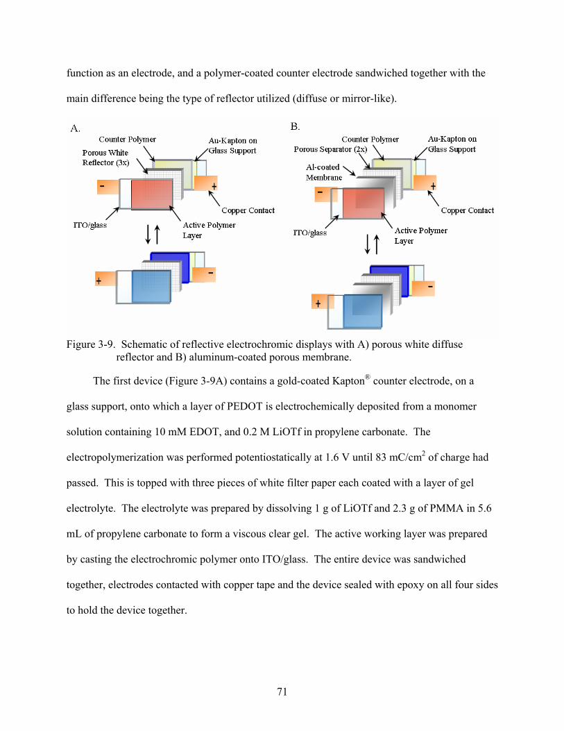
71
function as an electrode, and a polymer-coated counter electrode sandwiched together with the
main difference being the type of reflector utilized (diffuse or mirror-like).
Figure 3-9. Schematic of reflective electrochromic displays with A) porous white diffuse
reflector and B) aluminum-coated porous membrane.
The first device (Figure 3-9A) contains a gold-coated Kapton® counter electrode, on a
glass support, onto which a layer of PEDOT is electrochemically deposited from a monomer
solution containing 10 mM EDOT, and 0.2 M LiOTf in propylene carbonate. The
electropolymerization was performed potentiostatically at 1.6 V until 83 mC/cm2 of charge had
passed. This is topped with three pieces of white filter paper each coated with a layer of gel
electrolyte. The electrolyte was prepared by dissolving 1 g of LiOTf and 2.3 g of PMMA in 5.6
mL of propylene carbonate to form a viscous clear gel. The active working layer was prepared
by casting the electrochromic polymer onto ITO/glass. The entire device was sandwiched
together, electrodes contacted with copper tape and the device sealed with epoxy on all four sides
to hold the device together.
72
The second device, Figure 3-8B, is fabricated similar to the first device, except with an
aluminum-coated porous membrane and two pieces of filter paper sandwiched between the
working and counter electrodes. The metallized membrane was prepared by thermally
evaporating aluminum to 60 nm thickness onto porous polycarbonate membranes. With the first
device, device A, the white porous membrane acts as a paper-like diffuse reflector while in the
second device, device B, the aluminum membrane is the metallic mirror-like reflector. For both
devices, the active polymer layer is coated onto the ITO/glass that is inward facing. This is
different from the reflective ECD described in Chapter 2 in which the polymer was coated onto
the outward facing metallized porous membrane that functioned as the working electrode. As
the active polymer layer is cast onto a rigid substrate (ITO/glass), this allows for application of
the polymer by spray-casting or spin-coating, as is required for the active layer in the dual
EC/EL device. The reflective porous electrode detailed in Chapter 2 does not allow for spin-
coating of the polymer films given that the membranes are very thin (10 µm) and deformable and
highly porous. This is because the method by which substrates (the membranes in this case) are
secured to the spin-coater chuck is through vacuum suction. For that reason, electrodes coated
onto rigid substrates (glass or ~0.2 mm thick plastic film) are required.
To test the device designs, a model electrochromic polymer, with known reproducible
electrochromic behavior was utilized as the active layer. The polymer chosen for this study was
the previously mentioned PProDOT-(CH2OEtHx)2 for its ease of processability, high ambient
stability, and known electrochromic response in a device configuration.47 The active polymer
layer was prepared by spray-casting a solution of 5 mg/mL of PProDOT-(CH2OEtHx)2 in
toluene onto 1.5x1.5 cm ITO/glass slides. The spectroelectrochemical series of both devices
were measured using a Cary 500 UV/Vis-NIR spectrophotometer fitted with an integrating

73
sphere with the spectra of a reference device taken as the baseline. The reference device was
constructed with the same materials and same configuration as device A and device B, but with
no active polymer layer deposited on the working electrode. A potential sufficient to fully
neutralize the active polymer layer was applied across the device (-1.2 V) and the potential was
then stepped in 200 mV increments and held for 1 minute before each spectrum was taken. This
was continued until the fully oxidized state of the polymer was achieved. The
spectroelectrochemical series for both devices, A and B, containing a spray-cast film of
PProDOT-(CH2OEtHx)2 as the active layer are shown in Figures 3-10A and B.
Figure 3-10. Reflectance spectroelectrochemistry of spray-cast PProDOT-(CH2OEtHx)2 in an
electrochromic display with a A) porous white reflector and B) aluminum-coated porous membrane.
The absorbance of the polymer film was broad across the visible region with the maximum
absorbance centered around 550 nm. As oxidizing potentials are applied across the device, the
reflectance in the visible region begins to increase as was also seen for the same polymer film in
the reflective ECDs in Chapter 2. Similarly to the spectroelectrochemistry for MEH-PPV earlier
in this chapter, the λmax shifts to shorter wavelengths on oxidation of the polymer while a
decrease in the reflectance in the red region occurs. While this spectroelectrochemical series is
74
only taken of the visible region out to 800 nm, it is expected that the reflectance at longer
wavelengths would decrease on oxidation.
It can be seen that the active polymer layer is fully oxidized at +1.2 V for device A, with a
maximum contrast of 42% in the visible region. However, even beyond an applied voltage of
+1.5 V in device B, there remains a residual absorbance in the visible region with a maximum
contrast of 26%. This can be attributed to the aluminum porous reflector in this device. As the
device is switched over time it can be seen that the aluminum metal takes on a grey haze that
decreases the reflectance of this device, possibly due to oxidation. This also causes the
background correction taken with the reference device to no longer be adequate in correctly
subtracting contributions to the spectra from the device components not involved in the
electrochromic switching, such as the aluminum reflector. This could possibly be due to a side
reaction occurring in the electrochemical cell between the lithium triflate electrolyte in contact
with the aluminum electrode, causing corrosion of the aluminum while at the same time
reneutralizing the oxidized polymer layer, not allowing for full electrochromic switching.
To effectively model the electrochromic response of the luminescent conjugated polymers
in the dual EC/EL display, devices based on the designs of device A and device B were
constructed with the blends of the electroluminescent polymers with solid electrolytes as the
active layer. The blends were comprised of either MEH-PPV or Cbz2-Fl2 as the active
electrochromic material, LiOTf as the salt, and PEO as the ion solvator (for the MEH-PPV blend
only). The Cbz2-Fl2 blend does not contain PEO as this polymer contains ion-solvating
oligoethoxy side chains.
The MEH-PPV blend solution was made by preparing master solutions of the three
components separately. The master solutions were comprised of MEH-PPV, PEO, and LiOTf in

75
concentrations of 10 mg/mL, 13 mg/mL, and 13 mg/mL each in cyclohexanone, respectively.
The blend solution was then prepared by adding each component in a weight ratio of 10:3:1
(MEH-PPV:PEO:LiOTf) and diluting with cyclohexanone such that the final MEH-PPV
concentration was 5 mg/mL. The films were prepared by spin-casting the blend solution onto
ITO/glass slides at 1000 rpm to obtain a final thickness of 170 nm. Devices were constructed
with designs of device A and B with the MEH-PPV blend as the active electrochromic layer.
Figure 3-11A shows the spectroelectrochemical series for the electrochromic device A, with the
white paper reflector along with photographs of the device in the neutral (orange) and fully
oxidized (blue) states in Figure 3-11B Figures 3-11C and D show the spectroelectrochemical
series and photographs of the MEH-PPV device with the porous aluminum reflector (device
design B).
The maximum spectral contrast for the device based on design A was ~15% at 480 nm and
35% at 600 nm while that based on design B was ~60% at 480 nm and near 30% at 600 nm.
This difference in maximum contrast between the two devices at the shorter wavelength can be
explained by the incomplete oxidation of the polymer film in device A as seen in the photograph
in Figure 3-11B. As the encircled area of the photograph shows, there are portions of the film
that do not become oxidized to the blue color, but rather remain orange. This can be attributed to
the already high oxidation potential of this polymer along with the unevenness of application of
the gel electrolyte layer. In the areas where the polymer is not fully switched, the concentration
of gel electrolyte could be very thin, and switching of these areas are not as efficient, leading to
incomplete oxidation.
In the device based on design B, porous aluminum reflector, there are residual absorbances
at the high energy end of the spectrum (below 400 nm) and the low energy end of the spectrum
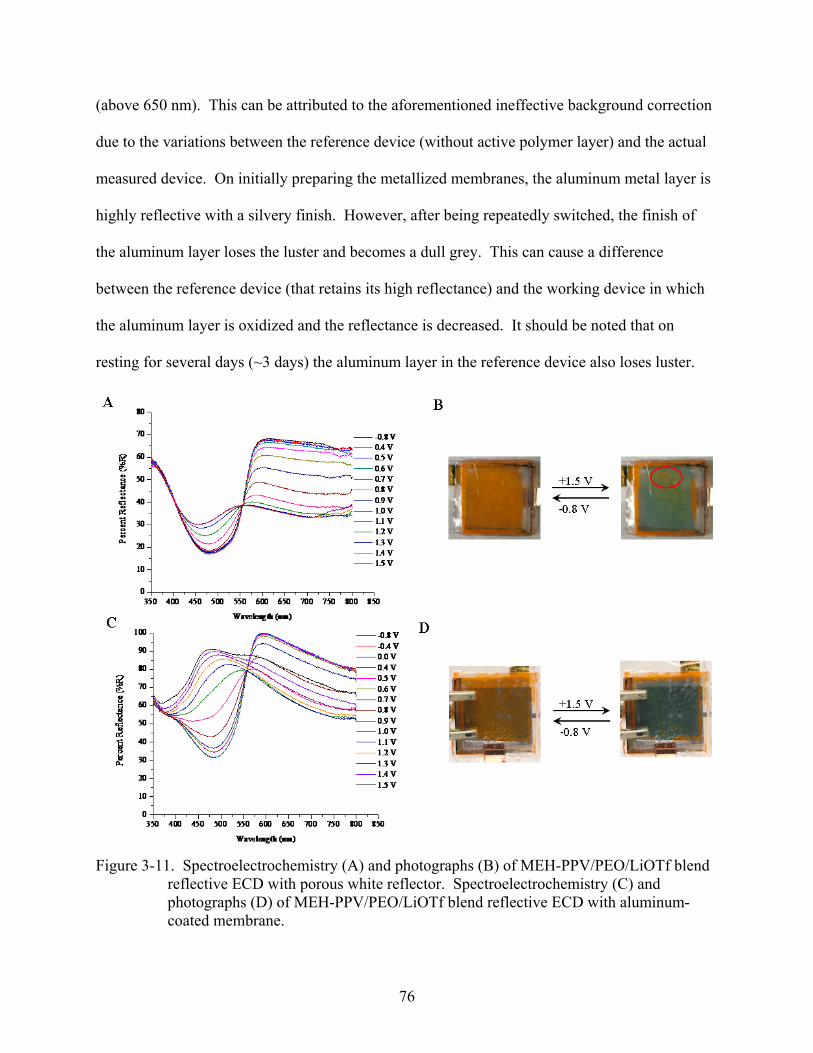
76
(above 650 nm). This can be attributed to the aforementioned ineffective background correction
due to the variations between the reference device (without active polymer layer) and the actual
measured device. On initially preparing the metallized membranes, the aluminum metal layer is
highly reflective with a silvery finish. However, after being repeatedly switched, the finish of
the aluminum layer loses the luster and becomes a dull grey. This can cause a difference
between the reference device (that retains its high reflectance) and the working device in which
the aluminum layer is oxidized and the reflectance is decreased. It should be noted that on
resting for several days (~3 days) the aluminum layer in the reference device also loses luster.
Figure 3-11. Spectroelectrochemistry (A) and photographs (B) of MEH-PPV/PEO/LiOTf blend
reflective ECD with porous white reflector. Spectroelectrochemistry (C) and photographs (D) of MEH-PPV/PEO/LiOTf blend reflective ECD with aluminum-coated membrane.
77
To further demonstrate an electroluminescent polymer as the electrochromic layer in a
reflective electrochromic device, Cbz2-Fl2 blended with LiOTf was utilized as the active layer in
both device designs A and B. A solution of Cbz2-Fl2 (5 mg/mL) blended with LiOTf in a
weight ratio of 20:4 in cyclohexanone was spin-cast onto ITO/glass at a rate of 500 rpm yielding
a film thickness of 47 nm. As mentioned previously, an ion solvating material, such as PEO, is
not needed as the polymer contains ion solvating oligoethoxy pendant groups. This leads to a
decreased solution viscosity compared to the MEH-PPV/PEO blend and makes producing thick
films by spin-coating difficult. Any future work involving this polymer would involve
investigating blending of the Cbz2-Fl2 with PEO. While the presence of oligoethoxy side-chains
is intended to solvate the LiOTf without the need for PEO, the side-chains could allow for
improvement of film quality and morphology on blending with PEO and other ion conducting
polymers
Spectroelectrochemistry of the Cbz2-Fl2/LiOTf blend as the active layer in device A and
device B are shown in Figure 3-12A and B, respectively. Both devices switched from a colorless
state to a pale orange color on oxidation, however the optical contrast was not high as the film
was rather thin and the polymer does not exhibit highly colored states as was also seen in the
photographs in Figure 3-6C. The device based on the porous white reflector (device A) had an
optical contrast of 20-25% at 500 nm, requiring a potential of at least 1.4 V to reach the oxidized
state. The device based on design B, porous aluminum reflector, exhibited a maximum contrast
of 30% at 500 nm. This device had little change in color or spectra until an applied potential of
2.0 V. As with the MEH-PPV device with the aluminum reflector, there is a residual absorbance
at longer wavelengths, possibly due to the difference in the reflectance of the reference device
compared to the active device.

78
Figure 3-12. Spectroelectrochemistry of Cbz2-Fl2/LiOTf blend reflective ECD with A) porous
white reflector and B) aluminum-coated membrane.
On comparison of the reflectance spectra of the device containing Cbz2-Fl2 as the active
layer and the absorbance spectra of that same polymer switched in a LiOTf/water electrolyte, a
peak for λmax is clearly seen for the film in the devices while none could be determined for the
films switched in water, while the onset for absorbance is at the same wavelength in all spectra.
This shift in the absorbance peak into the visible region can be attributed to solvent effects as the
film in the device is switched in a propylene carbonate-based gel electrolyte. It should be noted
that after switching both devices to the oxidized state, the polymer film would not completely
change color back to the neutral, colorless state. This is due to the high solubility of the polymer
in propylene carbonate, although as a gel, in which the polymer dissolves, not allowing it to be
further switched effectively. Due to this complication as well as the low optical contrast, this
polymer will not be further studied as a possible material in the dual EC/EL device and attention
will be focused on MEH-PPV as the active material for this specific study.
Conclusions
A newly designed reflective electrochromic display based on two different porous
reflective layers, white paper and aluminized membrane, has been demonstrated for the soluble
79
electrochromic polymer PProDOT-(CH2OEtHx)2 and two electroluminescent polymers MEH-
PPV and Cbz2-Fl2. These devices model the electrochromic half of the dual EC/EL display that
will be the focus of Chapter 4. While the devices introduced in this chapter effectively
demonstrated the possible utilization of two different electroluminescent polymers as the active
electrochromic layer, several modifications to the device would need to be made in further
studies to optimize display performance. Various salts, such as LiClO4, TBABF4, and even ionic
liquids, could be utilized as well as other ion-solvating materials such as crown ethers, and other
ionically conducting polymers. In addition, other reflective metals could be utilized in the place
of aluminum, such as gold, that are resistant to oxidation. The contrast of the white reflective
layer in device A could be optimized by using a white porous paper that does not darken when
wetted or applying a coating to the paper to increase the brightness of the white. This can be
achieved by utilizing a porous Teflon® membrane or coating the white filter paper with a white
laminate that is impervious to the solvents being used. Other electroluminescent materials can
also be investigated as the active layer such as ruthenium complexes, or other conjugated
electroactive polymers and copolymers. As the study to be detailed in Chapter 4 will be the first
demonstration of a dual EC/EL device, the focus of the work in this chapter has been placed on
demonstration of the device components to achieve the desired result of electrochromism and
electroluminescence from a single active layer at the same pixel in one device. It is expected that
further work to be conducted after this dissertation will focus on optimizing the proper
combination of materials and device designs to achieve the best device performance.

80
CHAPTER 4 DUAL ELECTROCHROMIC/ELECTROLUMINESCENT DISPLAYS
Conjugated conducting polymers are among a unique class of materials that exhibit a wide
variety of useful properties. As was discussed in Chapter 1, these polymers are electrically
conductive in the redox-doped state by either exposure to chemical oxidants/reductants or by
electrochemical oxidation/reduction. Some of the applications in which doped polymers are
used include antistatic coatings,174 electrochromic windows/displays,22 supercapacitors,19
actuators,24 and as transparent electrode materials.40 On the other hand, there have been a large
number of applications where the undoped form of conjugated polymers are useful as the
polymer backbone allows for charge carrier (electron and hole) transport within the valence or
conduction band. Some of these applications include photovoltaic devices,23 field-effect
transistors,21 and light-emitting diodes.20
The discovery of electroluminescence in conjugated polymers has been one of the most
important developments in the field as it has increased the interest of these materials for
consumer display devices. Since then, there has been much interest in improving device lifetime
and performance, and on producing colors that span the visible region by structural modification
of the polymer backbone, along with a number of techniques that include guest-host blends,
multi-layered structures, and others. Another development in the field of polymer light-emitting
displays are the light-emitting electrochemical cells (LECs), as is also described in Chapter 1,
that offer the advantage of device operation without the need for low work function, reactive
electrode materials. Devices have even been demonstrated with the same metal as both anode
and cathode where the electrodes are in a lateral arrangement with light emission occurring
between electrode lines separated by up to 1 mm.129
81
The most extensively utilized display in consumer electronics today is that based on liquid
crystal displays (LCDs).175 Typical LCDs contain either a light-source (transmissive) or a
reflective mirror behind the display elements (reflective). The transmissive devices operate by
varying the amount of light allowed to pass through the device while the reflective LCDs contain
a fully reflective mirror relying on ambient lighting or a front-light to provide illumination of the
image. While the transmissive, back-lit displays have excellent image quality in low lighting
situations, such as indoors, the quality is markedly diminished in situations where the brightness
of the ambient lighting is higher than that of the back-light used in the display, such as outdoors
in direct sunlight. A display able to be utilized in both low and high ambient lighting is that
based on transmissive-reflective, called transreflective, technology. This device contains both a
back-light and a reflective mirror. The mirror is partially reflecting, allowing some of the light
from the back-light to pass when the ambient lighting is low and reflects when the ambient
lighting is high. However, the brightness of the LCD indoors is not as high as with the
transmissive display as the partially reflective mirror decreases the amount of light transmitted
and the image quality is compromised in both modes compared to the fully transmissive or fully
reflective displays. In addition, LCDs have the added disadvantage of reduced viewing angle
and inability to fabricate mechanically flexible displays.
Another type of display is that based on microelectromechanical (MEMs) technology
introduced by QUALCOMM and known as an Interferometric Modulator Display, or IMOD.
This display is fabricated by placing a thin film mirror at a transparent substrate with a small gap
between that is several hundred nanometers with the gap acting as an optically resonant cavity.
Ambient light that strikes the display is reflected at the transparent substrate and the reflective
mirror. Depending on the distance between the mirror and the substrate, light of various

82
wavelengths are produced by constructive and destructive interference. The distance between
the thin film mirror and the transparent substrate is varied by the application of a voltage causing
the deformable mirror to collapse towards the substrate by electrostatic forces.176 As with other
reflective displays, an external light source is required to illuminate the device. This is
accomplished with either ambient lighting or a front-light.
A display that has been gaining interest is the electrophoretic display (EPD), also referred
to as electronic paper. Electrophoretic displays were designed to imitate the appearance of ink
on paper. Typically, the electronic ink is dark (blue or black) in color and is viewed against a
white background, providing a higher optical contrast than achieved with other displays. The
technology is based on a suspension of charged micron-sized white particles, such as titanium
dioxide, dispersed in an oil that is dyed with a dark ink. The suspension is encapsulated in
microparticles that are then placed between two parallel electrodes. When a positive potential is
applied to the top electrode, the negatively charged white particles migrate to the top of the
microcapsules and the viewer sees the white, highly reflecting, particles. A positive voltage is
then applied to the bottom electrode and the white particles migrate to the bottom of the
microcapsules, allowing the dark ink to now be seen by the viewer. This technology was
developed by E Ink Corporation, a spin-off from MIT’s Media Labs and through a partnership
with Philips, these displays have appeared in several consumer electronic devices such as Sony’s
Reader177 and Motorola’s Motofone.178 As with the other reflective displays, viewability relies
on an external light source and a front-light is necessary to view the display in low ambient
lighting.
This chapter details the design and operation of a device that, for the first time,
demonstrates electrochromism and light-emission from a single active layer at the same pixel. In
83
low ambient lighting situations, the display could be operated in the emissive mode without the
need for an additional light source. In high ambient lighting situations, as in direct sunlight, the
display would be operated in the electrochromic mode. The electrochromic function of the
display is modeled after the devices described in Chapter 3, while the emissive function of the
device is described within this chapter. Before description and demonstration of the dual
display, an investigation into the applicability of two types of polymer light-emitting displays
(the PLED and PLEC) are detailed. PLEDs were first investigated as there is a long established
history of these devices with published methods for fabrication and characterization data. This
allowed for a model device to establish a prototype for construction and development of methods
for device fabrication, analytical characterization, and materials performance along with
protocols for obtaining electrooptical data. These materials and methods were then applied to
the construction and characterization of PLECs, that are not as established in the literature and
require an added level of complexity in device construction and operation.
Polymer LEDs
The operating principle of PLEDs is given in Chapter 1 and shown in Figures 1-5 and 1-6
with the schematic of a typical device given in Figure 1-7. The device in this research was
constructed using a sandwich-type design with the ITO anode as the first layer. The ITO was
patterned and cleaned as detailed in Chapter 5. A thin (40 nm) layer of PEDOT:PSS was then
spin-coated onto the patterned ITO substrate and baked at 150ºC in a vacuum oven to remove
residual water. The PEDOT:PSS layer is used as a hole transport layer as it lowers the barrier
height for hole injection into the polymer layer.43, 84, 85 The PEDOT:PSS-coated substrates were
then transferred to an Argon atmosphere glove box with an oxygen content less than 0.5 ppm and
water content less than 0.1 ppm. The active electroluminescent polymer layer was then spin-
coated inside the glove box at various spin-rates for 30 seconds from a solution of 5 mg/mL of

84
MEH-PPV in chlorobenzene. The spin-rates used are 800, 1000, and 1200 rpm producing films
of approximately 70 nm in thickness as measured by AFM. The invariability in film thickness is
attributed to the low viscosity of the spin solution, and as has been shown previously, slight
increases in spin-rate has less of an affect on film thickness for solutions of lower
concentration.179 The films were then loaded into a thermal evaporator and the entire chamber
pumped down to 1 x 10⁻⁶ mbar for ~3 hours. The cathode material (10 nm calcium) was
thermally evaporated onto the films followed by 150 nm of an aluminum capping layer to protect
the cathode. Both metals are evaporated through a patterned shadow mask creating an active
pixel area of 7.07 mm2 with each device containing 8 pixels.
The electroluminescence of the devices were characterized by applying voltages across the
pixel with the ITO connected as the anode and Ca connected as the cathode while light output
was measured using the fiber-optic spectrometer, as described in Chapter 5, while inside the
glove box. To allow for complete fabrication and characterization of PLED devices, an MBraum
glove box system was established in which optical measurements are performed using a fiber-
optic spectrometer that allows remote measurement of light output from inside the glove box. To
accurately control the position of the fiber-optic cable relative to the device pixel, a X-Y-Z stage
was utilized and all device measurements were performed in an enclosed dark box fabricated in-
house. All optical measurements were taken normal to the device surface with the bare optical
fiber having a fiber diameter of 400 µm. The distance from the fiber-optic tip to the pixel is
chosen to allow the entire pixel area to be within the acceptance angle of the fiber-optic with an
additional 2.19 mm on each side of the pixel to allow for slight variations in positioning the
fiber-optic. This is shown schematically in Figure 4-1. The full acceptance angle (2 θ) of the
fiber-optic is 24.8º. By defining the radius of the circular area to be measured as 3.69 mm

85
(radius of emitting area of pixel plus the 2.19 mm on each side) and the half angle of acceptance
,θ, as 12.4º a distance can be determined by taking the ratio of the defined radius to the tangent of
the half angle, d = R’/tan θ, and is 16.8 mm.
Figure 4-1. Schematic of measurement geometry between fiber-optic probe and PLED pixel.
The optical measurements were performed using an Ocean Optics USB4000 spectrometer
as detailed in Chapter 5. The intensity of the light emitted from the pixel that is incident on the
fiber-optic is measured for the wavelength range of 400 to 800 nm and is recorded as the spectral
irradiance, Eλ. Spectral irradiance is defined as the radiance flux per unit area incident on a
surface and per unit wavelength interval at the wavelength λ, and is given by the equation:
Em = dmdE
= ds0 dmd 2U (4.1)
where Φ is the radiant flux (watts) and s0 is the area, and is given in units of µW cm-2 nm-1. As
the radiation emitting from the pixel is incident on the fiber-optic tip surface, the area is defined
by the fiber-optic tip area and is 1.26x10⁻³cm2. While the total power emitted from the pixel is
constant and uniform in all directions and is distributed over an area that increases with the

86
distance from the pixel squared, the irradiance drops off in proportion to the distance from the
pixel squared. Therefore, the distance between the pixel and fiber-optic tip, as defined in Figure
4-1, is kept constant for all measurements performed to allow comparison of irradiance
measurements at different voltages and different pixels.
The spectral irradiance measured for an individual MEH-PPV pixel operated at increasing
voltages is shown in Figure 4-2. At as low a voltage as 4 V, the spectral irradiance is 6.8x10⁻³
µW cm-2 nm-1 at 585 nm. As the voltage is increased, the intensity of the light emitted increases
to a maximum of 9.5x10⁻² µW cm-2 nm-1 with a shift in the peak wavelength of 13 nm to 572 nm
while the visually observed color is a constant orange-yellow as shown in the inset to Figure 4-2.
Figure 4-2. Spectral irradiance of an ITO/PEDOT:PSS/70 nm MEH-PPV/Ca/Al PLED pixel at
different applied voltages. Inset shows photograph of pixel operated at 9V.
The blue-shift in peak wavelength can be attributed to the increased contribution to the
electroluminescence spectra from shorter conjugation-length fractions in the polymer film that
emit at shorter wavelengths as higher voltages are applied. This is further supported by the

87
shoulder in the spectra at longer wavelengths that decreases in relation to the peak wavelength at
higher voltages. This longer wavelength emission is due to the longer conjugation-length
fractions in the polymer film that are present at a lower concentration and have a lower turn-on
voltage for emission. At higher voltages, the contribution from the higher concentration shorter
conjugation-length fractions begins to dominate.
Spectral irradiance is a unit of measurement of radiation and can include not only the
visible region of the spectra, but all electromagnetic radiation.180 Quantities such as spectral
irradiance, along with others not considered here, are defined as radiometric quantities. In the
display field, it is necessary to consider the response of the human eye to this radiation in the
visible region and therefore, a subset of radiometry has been defined that creates a relation
between the radiometric measurements and the human eye response and is called photometry. A
photometric quantity commonly used is luminance (Lv, units of cd m-2) and is a measure of the
subjective perception of brightness of a light source as a function of the area of the detector and
is the photometric equivalent to radiance and given by the following equation:
Lv = 683 Lm V (m) dm380
770
# (4.2)
The subscript, v, is used to indicate a photometric quantity, Lλ is spectral radiance and V(λ)
is the photopic spectral luminous efficiency as defined by the International Lighting Commission
(CIE) in 1924 and given in the IES Lighting Handbook.181 Spectral radiance is the area and solid
angle density of radiant flux per unit wavelength interval and has the units of watt m-2 sr-1 nm-1.
The solid angle is calculated by taking the ratio of the area of the pixel to the square of the
distance from the pixel to the fiber-optic tip (16.8 mm). This value is 0.025 sr for the
measurements detailed in this work. The factor 683 in the equation for luminance is an
additional constant necessary for the conversion of watts (radiometric) to lumens (photometric)
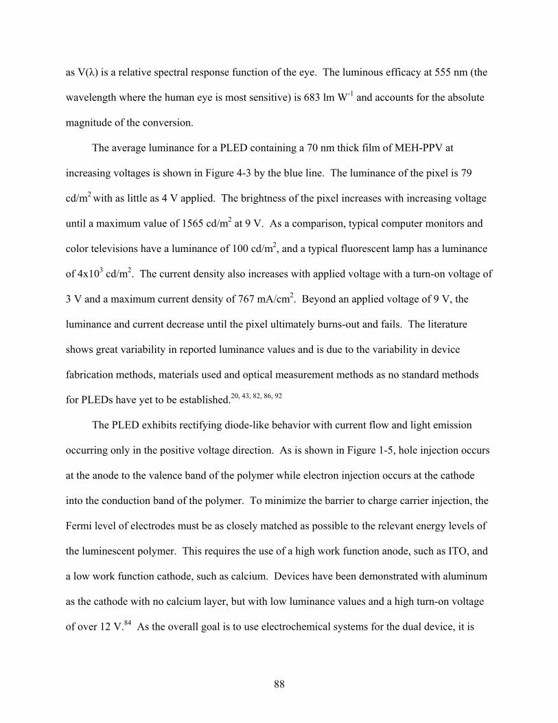
88
as V(λ) is a relative spectral response function of the eye. The luminous efficacy at 555 nm (the
wavelength where the human eye is most sensitive) is 683 lm W-1 and accounts for the absolute
magnitude of the conversion.
The average luminance for a PLED containing a 70 nm thick film of MEH-PPV at
increasing voltages is shown in Figure 4-3 by the blue line. The luminance of the pixel is 79
cd/m2 with as little as 4 V applied. The brightness of the pixel increases with increasing voltage
until a maximum value of 1565 cd/m2 at 9 V. As a comparison, typical computer monitors and
color televisions have a luminance of 100 cd/m2, and a typical fluorescent lamp has a luminance
of 4x10³ cd/m2. The current density also increases with applied voltage with a turn-on voltage of
3 V and a maximum current density of 767 mA/cm2. Beyond an applied voltage of 9 V, the
luminance and current decrease until the pixel ultimately burns-out and fails. The literature
shows great variability in reported luminance values and is due to the variability in device
fabrication methods, materials used and optical measurement methods as no standard methods
for PLEDs have yet to be established.20, 43, 82, 86, 92
The PLED exhibits rectifying diode-like behavior with current flow and light emission
occurring only in the positive voltage direction. As is shown in Figure 1-5, hole injection occurs
at the anode to the valence band of the polymer while electron injection occurs at the cathode
into the conduction band of the polymer. To minimize the barrier to charge carrier injection, the
Fermi level of electrodes must be as closely matched as possible to the relevant energy levels of
the luminescent polymer. This requires the use of a high work function anode, such as ITO, and
a low work function cathode, such as calcium. Devices have been demonstrated with aluminum
as the cathode with no calcium layer, but with low luminance values and a high turn-on voltage
of over 12 V.84 As the overall goal is to use electrochemical systems for the dual device, it is
89
desired not to use low work function metals as the high reactivity of the calcium layer is not
well-suited for use in a device that is to function as both an electrochromic and
electroluminescent device. In addition, doping of the electroactive polymer is known to quench
electroluminescence in PLEDs and switching of the active layer between neutral and oxidized
states during the electrochromic mode will not allow for further operation of the device in the
luminescent mode. A type of electroluminescent device with conjugated conducting polymers as
the active layer that would allow for operation without the need for low work-function metals
and could tolerate repeated doping/dedoping of the polymer layer is the LEC as described in
Chapter 1.
Figure 4-3. Current density (black) and luminance (blue) versus applied voltage for an average
of 4 pixels of an ITO/PEDOT:PSS/70 nm MEH-PPV/Ca/Al PLED.
Polymer LECs
The operating principle for a polymer LEC is shown in Figure 1-8. The device layout is a
sandwich-type of design as with the PLEDs. The ITO anode was patterned and cleaned in the

90
same manner as was described for construction of the LED devices. As no alignment of the
electrode work function with the polymer conduction/valence bands are necessary, a
PEDOT:PSS layer is not utilized in these devices. The active polymer layer contains a blend of
the electroluminescent polymer, MEH-PPV, an ion solvating polymer, PEO, and a salt, LiOTf.
Master solutions of each component were made by dissolving the material in cyclohexanone to a
concentration of 10 mg/mL, 13 mg/mL, and 13 mg/mL for the MEH-PPV, PEO, and LiOTf,
respectively. These solutions were allows to stir for 48 hours on a hotplate at a temperature of
40ºC to allow the solutes to completely incorporate into the solution. The blend solutions were
then made by mixing each component in a weight ratio of 10:3:1 (MEH-PPV:PEO:LiOTf) and
diluted with the appropriate amount of solvent so that the final MEH-PPV concentration is 5
mg/mL. This give a salt concentration of 3 mM. This weight ratio is one of the most commonly
referenced in the literature for the best performing devices. Further future studies on the dual
EC/EL displays would involve optimization of the blend components and relative weight ratios
for the best performance in both EC and EL mode and will be highlighted in the last section.
The polymer films were cast by spin-coating at spin-rates of 800, 1000, and 1200 rpm to
produce film thicknesses of 240, 170, and 75 nm, respectively. Given that this solution is
relatively viscous, the spin-rate has a more pronounced effect on the final film thickness than that
for the PLED device films. The most effective method for obtaining a film sufficiently thick for
optimum device performance (between 100 and 200 nm thick) by spin-coating is to use a fairly
concentrated solution. As the viscosity of this solution is higher than with the LED active layer
solution (5 mg/mL MEH-PPV in chlorobenzene) care must be taken to ensure that there are no
air bubbles remaining in the solution when it is dispensed onto the ITO substrate for spin-coating
as the air bubbles will cause holes to be present in the film, creating shorts when the cathode

91
layer is deposited. To remove air bubbles in the solution, the tip of the pipet was dragged
through the solution, across the substrate as the solution was dispensed. Lowering the viscosity
of the solution by dilution is not a satisfactory option as this decreases the active polymer layer
thickness on spin-coating to values that create devices that have a lower light output and a higher
incidence of shorts between the anode and cathode. As with the PLED devices, the cathode layer
(aluminum alone) was deposited by thermal evaporation through a shadow mask.
The devices were characterized in the same manner as the PLEDs with J-V measured using
a Keithley SMU and the EL spectra and luminance measured using the Ocean Optics USB4000.
The J-V and L-V curves for an average of 3 pixels for a MEH-PPV:PEO:LiOTf (10:3:1) LEC
with an active layer thickness of 170 nm and with ITO as the anode and aluminum as the cathode
is shown in Figure 4-4. An unexpected feature of these devices is that the light emission from
the device is very low for positive voltages but high for negative voltages. While ambipolar light
emission is expected, as has been shown in the literature and can be seen here with an onset for
increase in current density and luminance at ±3 V, better device performance is expected with
oxidation (p-doping) occurring at the ITO electrode and reduction (n-doping) occurring at the
aluminum.97
To date, little has been reported on both the positively and negatively biased J-V and L-V
characteristics of MEH-PPV:PEO:LiOTF LECs beyond the first paper to report these devices in
1995. On inspection of the results reported in that paper, it is actually unclear as to whether the
device performed better at negative voltages relative to positive voltages as the luminance seems
to level-off at the highest voltage they report (+4 V) while a leveling-off is not yet seen at the
highest negative voltage shown (-4 V).109 As seen in Figure 4-4, the maximum brightness in the
positive voltage direction is 39 cd/m2 with a current density of 170 mA/cm2 at 5 V. In the

92
negative voltage direction, the maximum brightness is 227 cd/m2 with a current density of -255
mA/cm2 at -8 V.
Figure 4-4. Current density (black) and luminance (blue) versus applied voltage for an
ITO/blend/Al PLEC with an active layer of a blend of MEH-PPV:PEO:LiOTf in a weight ratio of 10:3:1 at 170 nm thick.
On comparison of the current density and luminance for low applied voltages in both the
positive and negative directions, the luminance is higher for positive voltages up to ±5 V with
lower current densities. From the applied voltage of +5 to +6 V, the luminance decreases and the
current density more than doubles. On increasing the negative voltage, the luminance increases
and continues to do so until -8 V after which it decreases, possibly due to degradation of the
polymer blend at more negative voltages. A possible explanation for the cross-over in higher
luminance for positive voltages below 4 V to higher luminance for negative voltages greater than
-4 V is alteration of the aluminum contact to the polymer at these higher positive voltages. A

93
similar effect was observed as discussed in Chapter 3 for the aluminum-coated membranes used
in the reflective ECDs. The elucidation of the mechanism here is beyond the scope of this work.
It is also noticed that the current density peaks at a lower voltage, -7 V, than the luminance
and then begins to decrease. This can also be seen in Figure 4-5 for an average of three pixels in
a separate device with a 170 nm thick active layer. At voltages greater than -5 V, the current
essentially levels off. This can be attributed to the near-thin layer cell behavior of a PLEC
device. Between the voltages of -3 and -5 V, the majority of the current is devoted to setting up
of the p- and n-doped polymer junction. At voltages more negative than -5 V, the majority of the
current is devoted to maintaining the high concentration of doped polymer within the cell and
regenerating charge carriers as holes and electrons recombine within the p-i-n junction.
Figure 4-5. Current density (black) and luminance (blue) versus applied voltage for an average
of 3 pixels of an ITO/blend/Al PLEC with an active layer of a blend of MEH-PPV:PEO:LiOTf in a weight ratio of 10:3:1 at 170 nm thick.
The spectral irradiance of a pixel of a MEH-PPV LEC device with an active layer of 170
nm at increasingly negative voltages is shown in Figure 4-6. The spectra are very similar to that
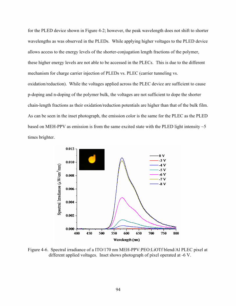
94
for the PLED device shown in Figure 4-2; however, the peak wavelength does not shift to shorter
wavelengths as was observed in the PLEDs. While applying higher voltages to the PLED device
allows access to the energy levels of the shorter-conjugation length fractions of the polymer,
these higher energy levels are not able to be accessed in the PLECs. This is due to the different
mechanism for charge carrier injection of PLEDs vs. PLEC (carrier tunneling vs.
oxidation/reduction). While the voltages applied across the PLEC device are sufficient to cause
p-doping and n-doping of the polymer bulk, the voltages are not sufficient to dope the shorter
chain-length fractions as their oxidation/reduction potentials are higher than that of the bulk film.
As can be seen in the inset photograph, the emission color is the same for the PLEC as the PLED
based on MEH-PPV as emission is from the same excited state with the PLED light intensity ~5
times brighter.
Figure 4-6. Spectral irradiance of a ITO/170 nm MEH-PPV:PEO:LiOTf blend/Al PLEC pixel at
different applied voltages. Inset shows photograph of pixel operated at -6 V.

95
In addition to device brightness and current density, relative device stability will be
another important factor for the device performance when incorporated into the dual EC/EL
display. Figure 4-7, shows that after an initial break-in cycle, the device shows little hysteresis
when cycling between 0 and -8 V and only an 8% drop in luminance between the 2nd and 3rd
cycles. While there will continue to be a slow decay, the rate of decay lessens. This is
encouraging as these devices were characterized without any form of packaging, allowing the
polymer layer and contacts to be fully exposed.
Figure 4-7. Luminance (A) and current density (B) as a function of applied voltage for an
ITO/blend/Al PLEC with an active layer of a blend of MEH-PPV:PEO:LiOTf in a weight ratio of 10:3:1 at 170 nm thick cycled between 0V and -8 V for three cycles.
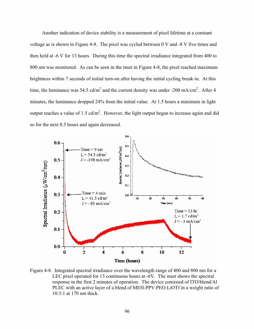
96
Another indication of device stability is a measurement of pixel lifetime at a constant
voltage as is shown in Figure 4-8. The pixel was cycled between 0 V and -8 V five times and
then held at -6 V for 13 hours. During this time the spectral irradiance integrated from 400 to
800 nm was monitored. As can be seen in the inset in Figure 4-8, the pixel reached maximum
brightness within 7 seconds of initial turn-on after having the initial cycling break-in. At this
time, the luminance was 54.5 cd/m2 and the current density was under -200 mA/cm2. After 4
minutes, the luminance dropped 24% from the initial value. At 1.5 hours a minimum in light
output reaches a value of 1.5 cd/m2. However, the light output began to increase again and did
so for the next 8.5 hours and again decreased.
Figure 4-8. Integrated spectral irradiance over the wavelength range of 400 and 800 nm for a
LEC pixel operated for 13 continuous hours at -6V. The inset shows the spectral response in the first 2 minutes of operation. The device consisted of ITO/blend/Al PLEC with an active layer of a blend of MEH-PPV:PEO:LiOTf in a weight ratio of 10:3:1 at 170 nm thick.

97
Previous researchers have also noticed a second increase in light emission after an initial
decline during lifetime measurements and attributed this to self-heating of the device.182 PEO is
a semicrystalline polymer at room temperature and these crystalline regions (60% of the bulk)
present barriers for ion diffusion with the ion transport preferentially occurring in the amorphous
phases.183 These crystalline regions begin melting at temperatures above room temperature
depending on the water content present in the PEO. Since great care was taken to effectively
remove the water from the PEO and handle the polymer in a dry atmosphere, it is expected that
the water content is minimal. The melting of the crystalline regions in PEO with weight
fractions of water less than 0.05 begins to occur at 30ºC.184 As these crystalline regions begin to
melt, the ionic conductivity of PEO then increases. This could then lead to the higher light
output after the initial decrease in device brightness as the charge carrier mobility is increased.
After several hours of operating at this higher temperature, the device inevitably begins to fail
with light output and current density decreasing to a minimum as seen in the lifetime experiment.
The work described here is the first in which the PEO component of the LEC blend is dried
to this extent. The technique used was lyophilization, a method to effectively remove water from
biological and pharmaceutical samples without destroying the sample as high temperature
techniques can do. With lyophilization, the sample, in this case PEO, was dissolved in the low
boiling point solvent, acetonitrile, that forms an azeotrope with water. The solution was then
quickly frozen in liquid nitrogen and placed under vacuum. As the sample is allowed to slowly
warm to room temperature, the acetonitrile/water azeotrope sublimes and collects at a water-
cooled condenser. LEC active layer blends made with this PEO were compared to PEO “dried”
as has been previously done throughout the literature by heating the sample in a vacuum oven to

98
40ºC. Figure 4-9 shows the L-V and J-V curves for the device containing the lyophilized PEO
(A) and the non-lyophilized PEO (B).
While both devices exhibit the same turn-on voltage at 3 V, the non-lyophilized PEO
device initially has a higher luminance and higher current density. At -6 V the non-lyophilized
PEO device has a luminance of 113 cd/m2 while the device containing the lyophilized PEO has a
luminance of 45 cd/m2 at that same voltage. However, the device with the non-lyophilized PEO
begins to fail with a drop in luminance and current density at voltages beyond -6 V while the
device containing the dry PEO continues to exhibit an increase in luminance at increasing
negative voltages until -10 V. The degree of crystallinity is dependent on the amount of water
present with PEO containing a higher weight fraction of water exhibiting a lower degree of
crystallinity. These results show that while the drier PEO may have a lower ionic mobility
(exhibited by the lower luminance) than the PEO with a higher percent of water present, the
device with the drier PEO shows a higher stability, operating efficiently to higher negative
voltages due to the absence of water that can have a detrimental effect on device performance.
It has been demonstrated that blends of MEH-PPV/PEO/LiOTf cast as thin films can be
utilized as the active layer in reflective electrochromic displays (Chapter 3) with ITO as the
working electrode and containing an aluminum-coated porous membrane as the reflective layer.
This chapter demonstrates that these blends of MEH-PPV with the solid electrolyte PEO/LiOTf
can also be utilized as the active layer in light-emitting electrochemical cells with light emission
occurring by n-doping at the ITO electrode and p-doping at the aluminum electrode. A device is
then constructed that is a combination of both of these devices, showing electroluminescence and
electrochromism from MEH-PPV at the same pixel.
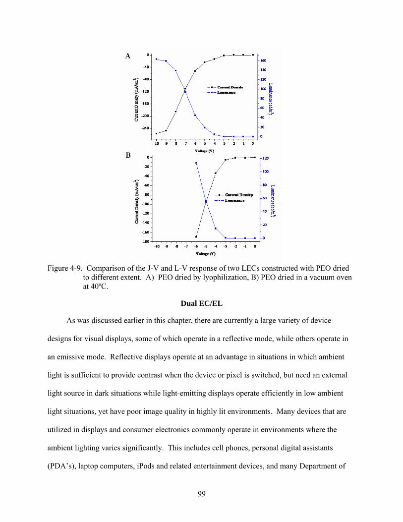
99
Figure 4-9. Comparison of the J-V and L-V response of two LECs constructed with PEO dried
to different extent. A) PEO dried by lyophilization, B) PEO dried in a vacuum oven at 40ºC.
Dual EC/EL
As was discussed earlier in this chapter, there are currently a large variety of device
designs for visual displays, some of which operate in a reflective mode, while others operate in
an emissive mode. Reflective displays operate at an advantage in situations in which ambient
light is sufficient to provide contrast when the device or pixel is switched, but need an external
light source in dark situations while light-emitting displays operate efficiently in low ambient
light situations, yet have poor image quality in highly lit environments. Many devices that are
utilized in displays and consumer electronics commonly operate in environments where the
ambient lighting varies significantly. This includes cell phones, personal digital assistants
(PDA’s), laptop computers, iPods and related entertainment devices, and many Department of
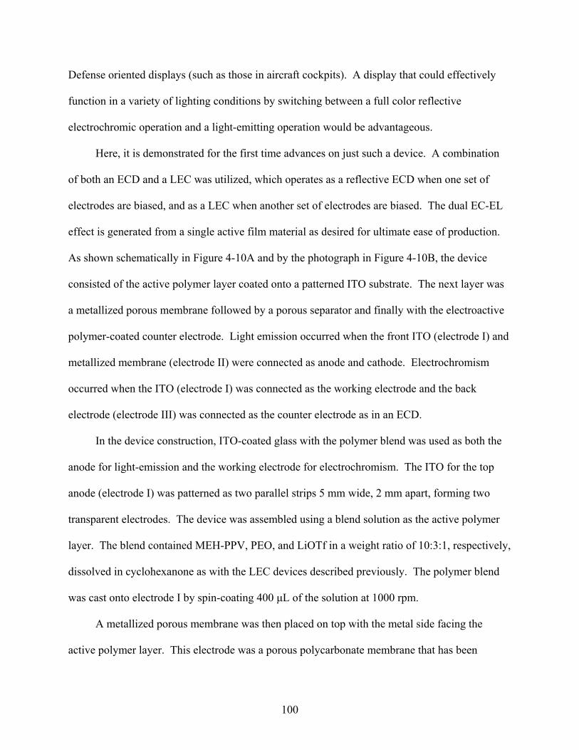
100
Defense oriented displays (such as those in aircraft cockpits). A display that could effectively
function in a variety of lighting conditions by switching between a full color reflective
electrochromic operation and a light-emitting operation would be advantageous.
Here, it is demonstrated for the first time advances on just such a device. A combination
of both an ECD and a LEC was utilized, which operates as a reflective ECD when one set of
electrodes are biased, and as a LEC when another set of electrodes are biased. The dual EC-EL
effect is generated from a single active film material as desired for ultimate ease of production.
As shown schematically in Figure 4-10A and by the photograph in Figure 4-10B, the device
consisted of the active polymer layer coated onto a patterned ITO substrate. The next layer was
a metallized porous membrane followed by a porous separator and finally with the electroactive
polymer-coated counter electrode. Light emission occurred when the front ITO (electrode I) and
metallized membrane (electrode II) were connected as anode and cathode. Electrochromism
occurred when the ITO (electrode I) was connected as the working electrode and the back
electrode (electrode III) was connected as the counter electrode as in an ECD.
In the device construction, ITO-coated glass with the polymer blend was used as both the
anode for light-emission and the working electrode for electrochromism. The ITO for the top
anode (electrode I) was patterned as two parallel strips 5 mm wide, 2 mm apart, forming two
transparent electrodes. The device was assembled using a blend solution as the active polymer
layer. The blend contained MEH-PPV, PEO, and LiOTf in a weight ratio of 10:3:1, respectively,
dissolved in cyclohexanone as with the LEC devices described previously. The polymer blend
was cast onto electrode I by spin-coating 400 μL of the solution at 1000 rpm.
A metallized porous membrane was then placed on top with the metal side facing the
active polymer layer. This electrode was a porous polycarbonate membrane that has been

101
patterned with a 60 nm layer of aluminum by thermal evaporation deposited in a pattern of two
parallel strips that were 5 mm wide and separated from each other by 2 mm. These strips were
patterned such that they lay perpendicular to the ITO-patterned strips, forming 4 separate pixels
that are 25 mm2 in area. This electrode acts as the cathode when the device is operated as a
light-emitting electrochemical cell.
Figure 4-10. Schematic of dual EC/EL device (A). Photograph of actual device (B).
The back electrode (electrode III) was ITO-coated glass on which PEDOT had been
electrochemically deposited as described in Chapter 3. This electrode acts as the counter
electrode when the device is operated as an electrochromic display. A separator paper, soaked in
electrolyte, was used to isolate the back of the metallized membrane from the counter polymer
layer as some of the metal can penetrate the membrane and short with the counter electrode. The
electrolyte consisted of 5 mg/mL PEO and 0.9 mg/mL LiOTf dissolved in ACN.

102
Before assembly, the solvent was allowed to evaporate, leaving behind a solid electrolyte.
In addition, a layer of the solid electrolyte was also deposited onto the PEDOT layer and allowed
to dry before device construction. This was to ensure a sufficient concentration of ions for
electrochromic operation of the device. All electrodes were contacted with copper tape and the
device was sealed with epoxy on the edges. With this design, only the active polymer layer is
responsible for the light-emission and electrochromism observed, while the counter electrode
polymer is used for charge balance during electrochromic switching.
As the top ITO anode and the middle metallized porous cathode are connected to a voltage
source, light emission occurs from the active polymer layer. After the addition of a small
amount of ACN to improve ion mobility (~250 μL), the front ITO electrode was connected to a
potentiostat as the working electrode and the back PEDOT-coated ITO electrode was connected
as the counter electrode. When the device was biased with positive voltages applied to the
working electrode, the active polymer layer electrochromically switched between a neutral
orange-red color to an oxidized blue color. The device was then biased with negative voltages
applied to the working electrode and the active polymer layer switched back to the orange-red
neutral state. It should be noted that the utilization of a lower viscosity electrolyte should
improve ion mobility during electrochromic switching, thereby eliminating the need for the
addition of small amounts of solvent during electrochromic switching.
As is shown in the photographs in Figure 4-11A (entire device) and D (close-up of a pixel
from a different device), when the ITO electrodes were connected as the anode and the porous
aluminum electrodes connected as the cathode, the pixels emitted light when -21 V was applied.
This high voltage for light emission is expected as there is poor contact between the polymer
film and the aluminum electrode. This can be improved in further studies by evaporation of a
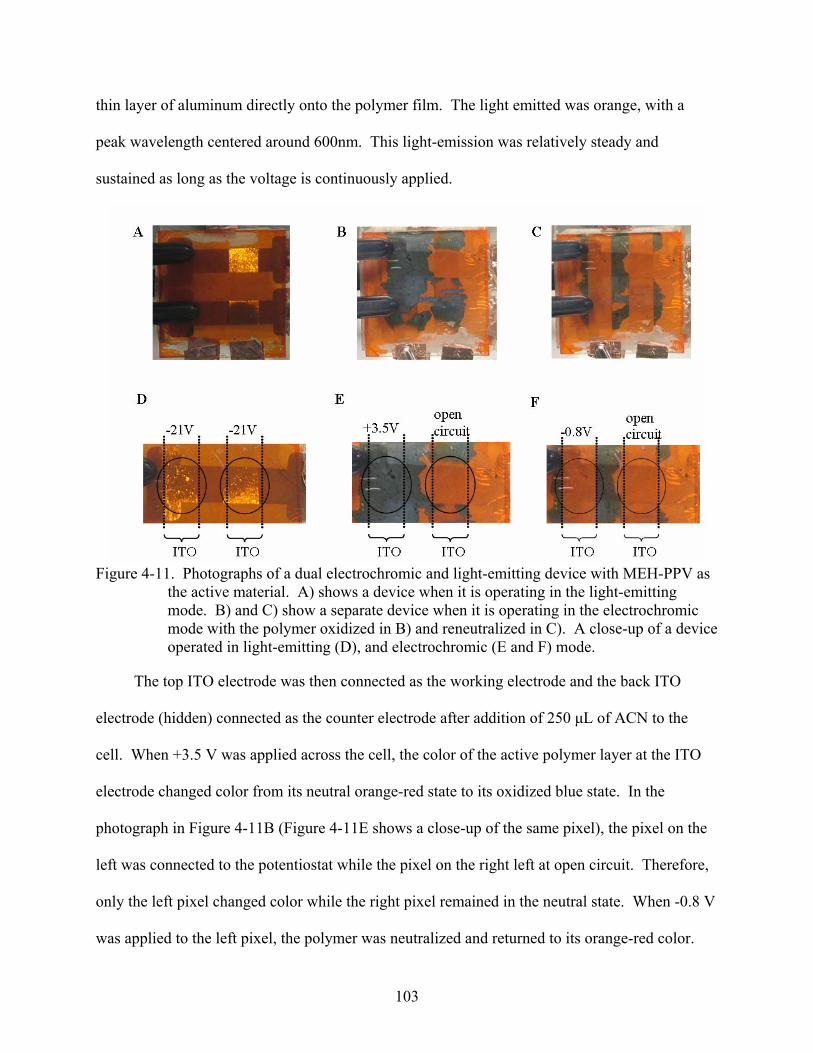
103
thin layer of aluminum directly onto the polymer film. The light emitted was orange, with a
peak wavelength centered around 600nm. This light-emission was relatively steady and
sustained as long as the voltage is continuously applied.
Figure 4-11. Photographs of a dual electrochromic and light-emitting device with MEH-PPV as
the active material. A) shows a device when it is operating in the light-emitting mode. B) and C) show a separate device when it is operating in the electrochromic mode with the polymer oxidized in B) and reneutralized in C). A close-up of a device operated in light-emitting (D), and electrochromic (E and F) mode.
The top ITO electrode was then connected as the working electrode and the back ITO
electrode (hidden) connected as the counter electrode after addition of 250 μL of ACN to the
cell. When +3.5 V was applied across the cell, the color of the active polymer layer at the ITO
electrode changed color from its neutral orange-red state to its oxidized blue state. In the
photograph in Figure 4-11B (Figure 4-11E shows a close-up of the same pixel), the pixel on the
left was connected to the potentiostat while the pixel on the right left at open circuit. Therefore,
only the left pixel changed color while the right pixel remained in the neutral state. When -0.8 V
was applied to the left pixel, the polymer was neutralized and returned to its orange-red color.
104
This can be seen in Figure 4-11C (and the close-up of the same pixel in Figure 4-11F), where the
pixel on the left is again orange-red. The pixel on the right is still at open circuit. These pixels
can be repeatedly switched between the two color states.
Overview and Future Directions
While the ultimate goal of this chapter to demonstrate a dual electrochromic/
electroluminescent device has been attained, many key concepts and methods were also
demonstrated and established. Many device construction and measurement methods were
established with the fabrication of standard MEH-PPV PLEDs with complete fabrication in an
inert atmosphere glovebox along with optical characterization using a new fiber-optic system.
This allowed for the creation of a protocol for further analytical characterization of materials and
devices of the more complicated PLECs. These PLEC devices, never before demonstrated in our
laboratory, were constructed with a MEH-PPV/PEO/LiOTf active blend layer with the onset for
light-emission occurring at ±3V and maximum luminance values on par with those reported in
the literature. As the operational behavior of this type of device was observed with reproducible
results, it allowed the incorporation of the LEC concept into the dual EC/EL device. The
reflective electrochromic and light-emitting cell designs were then integrated into a single device
where both electrochromism and electroluminescence were shown.
While this is the first time it has been demonstrated for a display device to exhibit both
electrochromism and electroluminescence from the same pixel, there are yet a number of future
modifications to the device components or design that could be made to improve device
performance, as with any proof-of-concept. A possible alternative would be to investigate the
possibility of other solid electrolytes by varying the salt and/or the ionically conducting polymer.
As was also mentioned, PEO is a semicrystalline polymer and the presence of crystalline regions
inhibits ionic mobility within this phase. Other ion-solvating polymers that have a higher

105
amorphous content at room temperature could possibly offer an improvement over PEO.
However, care must be taken to choose a salt that is easily solvated by the ionically conducting
polymer and both the salt and ion-solvating polymer would need to be soluble in a common
solvent with the emissive polymer and this requirement further limits the choice in solid
electrolyte. Several researchers have shown that either salts complexed with crown ether-based
systems or ionic liquids as attractive choices in LEC devices.115, 120
There also exists the possibility of utilizing other electroluminescent polymers in the dual
EC/EL to achieve a wide range of colors not only for light emission, but also electrochromism.
The requirement for a polymer to be utilized in this device is that it exhibit emission in the solid
state, have a HOMO level high enough to allow oxidation of the polymer during electrochromic
switching at readily accessible potentials, and have an accessible reduction potential.
In addition, alternative device designs are another possibility to overcome some of the
limitations encountered and improve device performance. One such device would be the
planar/lateral device. This device would be comprised of an interdigitated microelectrode (IME)
on a substrate that has been coated with the active blend layer. This is then followed by a porous
separator and a counter electrode coated with a counter polymer layer as is shown in the
schematic in Figure 4-12. For light emission, the interdigitated electrodes I and II are contacted
as the anode and cathode with light emission occurring between the fingers. For
electrochromism, both interdigitated electrodes I and II are shorted together as the working
electrode and the polymer-coated back electrode III is connected as the counter electrode.
For initial experiments, the IMEs could be purchased from a commercial source that offers
line widths and line spacings from 5 to 20 µm with electrode materials such as gold, platinum,
and ITO on glass. Previous research by Heeger et al., has demonstrated the concept of a lateral
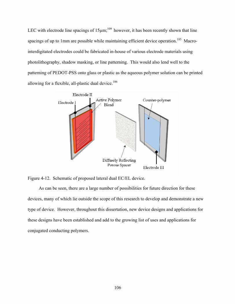
106
LEC with electrode line spacings of 15µm;109 however, it has been recently shown that line
spacings of up to 1mm are possible while maintaining efficient device operation.185 Macro-
interdigitated electrodes could be fabricated in-house of various electrode materials using
photolithography, shadow masking, or line patterning. This would also lend well to the
patterning of PEDOT-PSS onto glass or plastic as the aqueous polymer solution can be printed
allowing for a flexible, all-plastic dual device.186
Figure 4-12. Schematic of proposed lateral dual EC/EL device.
As can be seen, there are a large number of possibilities for future direction for these
devices, many of which lie outside the scope of this research to develop and demonstrate a new
type of device. However, throughout this dissertation, new device designs and applications for
these designs have been established and add to the growing list of uses and applications for
conjugated conducting polymers.
107
CHAPTER 5 INSTRUMENTATION AND EXPERIMENTAL TECHNIQUES
As this dissertation covers various, differing, applications of conjugated electroactive
polymers, a large variety of techniques have been utilized in fabrication of devices and their
subsequent characterization. This chapter sets forth to present an overview of the materials,
techniques, and instrumentation used during the course of this research.
Chemicals and Materials
Reagent grade acetonitrile (ACN), propylene carbonate (PC), and cyclohexanone in Sure
Seal® bottles were purchased from Aldrich. Chloroform (Aldrich) and ACN were distilled over
CaH2. PC was percolated through activated type 3A molecular sieves, followed by fractional
distillation under reduced pressure. Cyclohexanone was directly transferred to a Schlenk flask
under Argon by cannula, followed by freeze-pump-thaw for three cycles and stored in the
glovebox. Solvents used in the glovebox were deoxygenated by freeze-pump-thaw before being
transferred into the glovebox. Solvents used on the bench were stored under Argon and purged
for a minimum of 10 minutes prior to use.
Tetrabutylammonium hexafluorophosphate (TBAPF6- Fluka), lithium perchlorate (LiClO4
- Alrich), and lithium trifluoromethanesulfonate (LiCF3SO3 – Aldrich) were dried under vacuum
at 150ºC for 24 hours prior to use. Poly(methyl methacrylate) (PMMA) (Mw 85,000 g/mol, PDI
2.4) was purchased from Aldrich and used without further purification. Poly(ethylene oxide)
(PEO - Aldrich) (Mw 1,000,000 g/mol) was dried by lyophilization (as detailed in Chapter 4)
from ACN prior to use. Poly(3,4-ethylenedioxythiophene)/poly(styrene sulfonate)
(PEDOT:PSS) (Baytron P VP Al 4083) was purchased from H.C. Starck and syringe filtered
through a 0.45 micron Nylon filter followed by filtering through a 0.2 micron Nylon filter prior
before use. The monomer, EDOT (Baytron M V2) was purchased from H.C. Starck and distilled
108
under vacuum from CaH2. Poly[2-methoxy-5-(2-ethylhexyloxy)-1,4-phenylenevinylene], MEH-
PPV (OPA6345) (Mw 175,000 g/mol, PDI 1.3) was purchased from H.W.Sands and used as
received. Poly(3,3-bis(2-ethylhexyloxymethyl)-3,4-dihydro-2H-thieno[3,4-b][1,4]dioxepine)
(PProDOT-(CH2OEtHx)2) (Mw 75,000, PDI 1.6), and poly(3,3-dihexyl-3,4-dihydro-2H-
thieno[3,4-b][1,4]dioxepine) (PProDOT-Hx2) (Mw 66,000 g/mol, PDI 1.7) were prepared as
previously reported.48 Poly[(9,9-bis(methoxyethoxyethyl)-2,7-fluorene)-alt-(N-
(methoxyethoxyethyl)-3,6-carbazole)] (Cbz2-Fl2), and poly[(1,4-
bis(methoxyethoxyethoxyethoxy)-2,5-phenylene)-alt-(N-(methoxyethoxyethyl)-3,6-carbazole)]
(Cbz2-Ph3) ,whose structures are shown in Figure 3-2, were synthesized specifically for this
study.187 Briefly, the polymers were synthesized by Suzuki coupling between the diboronate of
the carbazole monomer and the corresponding aromatic dihalide (phenyl or fluorene) monomer.
The polymerizations required equimolar amounts of 3,6-di(dioxaborolanyl)-N-
methoxyethoxyethyl-carbazole and the aromatic dihalide (1,4-dibromo-2,5-
bis(methoxyethoxyethoxyethoxy)benzene or 2,7-dibromo-9,9-bis(methoxyethoxyethyl)fluorene)
were added to a solution of Aliquat 336 in toluene and bubbled with Argon. To this, a 2M
aqueous solution of sodium carbonate was added with freshly prepared palladium
tetrakis(triphenyl phosphine) and refluxed at ~105oC for three days. The organic layer was
collected, concentrated by evaporation and the product isolated by dissolving in dichloromethane
followed by precipitation into methanol. The polymer was collected by filtration and dried under
vacuum.
ITO-coated glass slides were purchased from Delta Technologies (CG-50IN-CUV and CB-
50IN-0111). Prior to use, the ITO slides were cleaned by light mechanical rubbing with a cotton
swab soaked in a surfactant solution (aqueous sodium dodecylsulfate). This was followed by
109
rinsing in a stream of distilled water, then acetone and isoproanol, then air dried. Track-etched
polycarbonate membranes were purchased from GE Osmonics Inc. Membranes are 10 microns
thick with 10 micron diameter cylindrical pores. Gold (99.99% pure) was purchased locally
(National Coin Investors, Inc.). Platinum wire and sheets, silver wire, and aluminum slugs were
purchased from Alfa Aesar. Platinum button electrodes were purchased from BAS. ITO/glass
interdigitated microelectrodes (IME 1050.5-M-ITO-U) were purchased from AbTech Scientific.
The digit length was 5 mm with 10 micron line width and 10 micron spacing between digits.
Gold-coated Kapton® (100 nm thick gold layer on 1 mm thick Kapton® sheets) was purchased
from Astral Technologies and cut to size with scissors. Copper tape, used to contact ITO and
Au-coated membrane electrodes was purchased from 3M electronics division.
Device Construction
Electrochromic Displays
The gel electrolyte used in the devices was composed of either 1 g of TBAPF6 or 0.4 g of
LiOTf , dissolved with 2.3 g of PMMA, in 5.6 mL of PC giving a salt concentration of 0.46 M.
The gel was prepared by dissolving the salt in PC, followed by slowly adding PMMA while
stirring and heating to 60ºC until all components were incorporated to form a highly viscous
clear gel. Gold- or aluminum-coated polycarbonate membranes were prepared by thermally
evaporating the metal using a high vacuum thermal evaporator (Denton DV-502A) operated at
1x10⁶ mbar. The membranes were sandwiched between an aluminum plate and a patterned
mask. The metals were deposited to a final thickness of 60 nm at a deposition rate of 4 Å/sec.
The reflective ECDs as described in Chapter 2, were fabricated by sandwiching together
several layers. The fabrication, from bottom to top, began with an acetate (3M transparency
film, PP2500) support onto which the counter electrode was placed. The counter electrode
consists of a gold-coated Kapton® electrode (contacted with copper tape) with an

110
electropolymerized layer of PEDOT. The PEDOT was polymerized using potentiostatic
conditions at 1.6 V vs. Ag wire until a deposition charge of 200 mC has passed. The monomer
solution contained 10 mM EDOT and 0.2 M TBAPF6 in PC. This layer is left in the oxidized
form for device construction. The next layer is three pieces of filter paper (Fisherbrand, 09-803-
5A) that are soaked in the gel electrolyte. This is followed by the outward facing working
electrode, which is the gold-coated polycarbonate membrane.
The active electrochromic polymer layer is applied to this electrode by either spray-casting
or electropolymerization. Spray-casting was performed using a 5 mg/mL solution of the desired
polymer in toluene that is sprayed from a commercial airbrush (Testors Corp., Aztek TS28)
operated at an air pressure 20 psi. Electrochemical polymerization was performed by applying a
potential high enough to oxidize the monomer (typically 1.2 to 1.6 V vs. Ag wire) in a solution
of 10 mM monomer, 0.2 M TBAPF6. This potential was held until the desired polymer thickness
was achieved as determined by passed charge density, with values typically ranging from 3 to 17
mC/cm2. The active polymer layer thickness was typically equal to or less than the PEDOT
counter layer thickness, which ensured full switching of the working electrode. A transparent
window (3M transparency film, PP2500) was placed on top and the entire device sealed on all
four edges using transparent tape. The device schematic and photographs can be seen in Figure
2-1A and B.
The ECDs described in Chapter 3 were fabricated similarly; differing in the type of
reflector and working electrode. The counter electrode was the same as described above
(PEDOT on Au-Kapton®). For the device containing the aluminum reflector, the counter
electrode was followed by two pieces of gel electrolyte-soaked filter paper. The next layer was
an aluminum-coated polycarbonate membrane that is outward facing (as shown in Figure 3-9B).
111
The working electrode is ITO/glass on which the active electrochromic layer was spin-cast. The
working and counter electrodes were contacted with copper tape and the entire device sealed
with epoxy on all four edges. For the device containing the white paper reflector (Figure 3-9A),
the counter electrode was followed by three pieces of gel electrolyte-soaked filter paper. The
working electrode is again ITO/glass coated with the active electrochromic layer by spin-casting.
Polymer Light-Emitting Diodes
Polymer LEDs were prepared by first etching the ITO/glass (25 x 25 mm) to create an
anode pattern. The pattern for ITO etching can be found in the dissertation by a previous
doctoral student in the Reynolds group.188 The ITO was covered with clear packing tape
(ScotchTM Brand) and the pattern cut out using a razor blade. The unmasked areas of ITO were
etched by exposure to aqua regia vapors (3:1 HCl:HNO3) for ten minutes. The etched ITO was
cleaned as described previously. The electrodes were placed in an oxygen plasma cleaner for 30
minutes. The PEDOT:PSS hole transport layer was spin-coated onto the ITO electrodes at 4000
rpm to a final thickness of 40 nm. The electrodes were baked in a vacuum oven at 150ºC for 12
hours. The substrates were transferred to an Argon atmosphere drybox where the remaining
device fabrication and characterization took place. The active electroluminescent layer was
applied by spin-coating a solution of 5 mg/mL MEH-PPV in chlorobenzene at various spin rates
for 60 seconds. The devices were transferred to a thermal evaporator and the cathodes were
deposited at a pressure of 1 x 10⁻⁶ mbar. The first layer was calcium deposited to 10 nm
followed by 150 nm of aluminum through a shadow mask giving an active pixel area of ~7.07
mm2. The pattern for the shadow mask is as previously described.188
Polymer Light-Emitting Electrochemical Cells
Polymer LECs were fabricated in a similar manner as the LEDs. The ITO/glass anodes
were patterned and cleaned by the same methods. The difference being that there is no

112
PEDOT:PSS hole transport layer. After cleaning, the electrodes were immediately transferred to
the glovebox. The electroluminescent layer was spin-cast onto the ITO anodes at various spin
rates for 60 seconds. The LECs master solutions contained the electroluminescent polymer,
PEO, and LiOTf each at a concentration of 10 mg/mL, 13 mg/mL, and 13 mg/mL in
cyclohexanone, respectively. The MEH-PPV blend was prepared by combining each component
in a weight ratio of 10:3:1 and diluted to a MEH-PPV concentration of 5 mg/mL. The carbazole
copolymer blend solutions were prepared by adding LiOTf to the polymer master solution to
form a weight ratio of 20:4 with a final copolymer concentration of 10 mg/mL. The films were
then transferred to the thermal evaporator and an aluminum cathode was thermally evaporated to
a thickness of 150 nm through the same shadow mask described for the PLEDs.
Dual Electrochromic/Electroluminescent Devices
The layered dual EC/EL devices (as shown in Figure 4-10) were fabricated based on the
combination of the standard LEC device and the aluminum reflector electrochromic device
design. The first layer of this device is comprised of a PEDOT-coated gold/Kapton® counter
electrode on a glass support. The next layer is two pieces of filter paper soaked with a LiOTf-
based gel electrolyte. On that layer is the aluminum-coated porous membrane that acts as both a
cathode for light-emitting operation and a reflective metal for the electrochromic operation. The
deposited aluminum is patterned in two strips that are 5 mm in width and 10 mm apart. The
active layer is comprised of MEH-PPV:PEO:LiOTf in a weight ratio of 10:3:1 in cyclohexanone
(as with the LECs) spin-cast on the ITO anode. The ITO is patterned on the anode in two strips
that are 5 mm in width and 10 mm apart (as with the cathode). The strips are arranged
perpendicular to the aluminum strips such that the active light-emitting pixel area is defined by
the overlap between the aluminum and ITO electrodes and is 25 mm2. The entire device was
sealed with epoxy on all four edges. Operation of the device is described in detail in Chapter 4.

113
Electrochemical Methods
The electrochemical methods used in polymer electrochemistry have been extensively
reviewed by previous researchers in the Reynolds group.189, 190 Therefore, the methods specific
to this work will briefly be covered here. All electrochemical measurements were performed
with an EG&G PAR model 273A potentiostat controlled using CorrWare software (Scribner
Associates)
Electropolymerization
The potential for electropolymerization of a monomer is typically determined by cycling
the potential of a working electrode and monitoring the resulting current. Once the peak current
for monomer oxidation is determined, that potential is used for subsequent potentiostatic
electropolymerization experiments. The typical electrochemical cell setup is comprised of a
working electrode, reference electrode, and counter electrode in a glass cell. The working
electrodes used in this work include ITO/glass, gold-coated polycarbonate membranes, and gold-
coated Kapton®. Electrical contact to these electrodes was made with copper tape. The
electrode is immersed in the monomer solution in the glass cell. The setup also includes a
counter electrode that is a platinum flag made by spot-welding platinum wire to platinum foil.
The size of the foil is such that the area of the counter electrode is always larger than the area of
the working electrode to be used. The reference electrode is a silver wire pseudoreference that is
frequently (every half-hour) calibrated with a standard ferrocene solution (5 mmM ferrocene, 0.2
M LiClO4, ACN). Monomer solutions are composed of 10 mM monomer in 0.2 M salt (either
TBAPF6 or LiOTf) in propylene carbonate and are bubbled with Ar for at least ten minutes.
During the potentiostatic electropolymerization, the oxidizing potential is applied to the
working electrode. This polymerization is terminated when a specific charge has passed where
the charge is determined in previous experiments in which a calibration plot of charge versus

114
final film thickness is prepared for each monomer. By this method the resulting polymer film
thickness can be chosen by setting the potential to be applied until the necessary charge has
passed. The polymer films are then rinsed with fresh solvent and electrochemically switched in
monomer-free electrolyte.
Polymer Electrochemistry
Electrochemistry of polymer films, whether prepared by spray-casting, drop-casting, or
electropolymerization, is performed in a three-electrode cell. This cell is described as above with
the polymer-coated electrode as the working electrode, a platinum flag as the counter electrode,
and a Fc/Fc+-calibrated silver wire as the reference electrode. The film is switched by cycling
the electrode potential using cyclic voltammetry (CV) in an electrolyte solution of 0.2 M salt in
either PC, ACN, or water that has been bubbled with Argon for ten minutes. An Argon blanket
is kept over the solution during the measurements. The potential applied to the working
electrode is scanned to a value sufficient to oxidize the polymer and cycled back to the beginning
while the current is measured. Polymer films typically require a break-in of at least five scans
before repeated cycling of the potential is stable to ion and solvent diffusion in and out of the
film. If an anodic and cathodic peak are clearly visible, the E1/2 of the polymer is then
determined by summing the peak cathodic current with the peak anodic current and dividing
their sum by 2. If an anodic peak current is not clear, the onset for the current increase on
oxidation is determined and reported.
Optical Methods
Spectroelectrochemistry
Benchtop spectroelectrochemical measurements were performed with a Varian Cary 500
UV/Vis-NIR spectrophotometer. Polymer films to be measured on ITO/glass were placed in a
standard 1 cm cuvette fitted with a Teflon cap to hold the ITO/glass in place along with the
115
reference and counter electrode wires. These wires were placed on either side of the cuvette so
as to not block the source beam or come into contact with the working electrode. The cuvette
was filled with the appropriate electrolyte solution that has been purged with Argon for 10
minutes. The baseline is taken as an identical cell to the one to be measured minus the polymer
film. The electrodes were connected to a potentiostat and the desired potential applied to the
working electrode and held while the wavelength region of interest was being scanned. An
electrochemical break-in scan of the film is performed before the spectroelectrochemical series is
performed, except where noted. Spectroelectrochemical measurements performed in the
glovebox were done using a StellarNet EPP2000 Vis-NIR fiber-optic spectrophotometer. The
instrument contains a SL1 calibrated light source and a photo diode array detector. The fiber-
optic cables allowed remote measurement of the polymer spectra from inside the glovebox.
Benchtop reflectance spectroelectrochemistry of ECDs was performed using the Cary 500
spectrophotometer with an integrating sphere attachment mounted to the instrument. The inside
of the sphere is coated with highly reflective BaO and has a sample and reference port. The
device is placed at the sample port while a BaO standard is placed at the reference port. The
baseline is taken using a reference device that is constructed with the same components as the
sample device, except for the active polymer layer. The reflectance measured is total reflectance
and is comprised of both specular and diffuse light. The device is connected to a potentiostat
with the working electrode connection to the active electrode. The reference and counter
connections are shorted together and connected to the counter electrode of the device. A
potential is applied across the device and held while the wavelength region of interest is scanned.
Reflectance measurements using the fiber-optic spectrometer were performed using the
setup described in Chapter 2. The device is placed (face up) between the two plates of the
116
sample holder and the input and output fibers are attached. The light measured from the device
is specular only at a 45º angle. The schematic and photograph of the device holder is shown in
Figure 2-12.
Electroluminescence Measurements
Electroluminescence of PLEDs and PLECs was measured using an Ocean Optics
USB4000 fiber-optic spectrometer containing linear CCD array detector. The response of the
detector is calibrated on a monthly basis using a standard LS-1-CAL light source. This allowed
measurements to be performed in the glovebox under an Argon atmosphere. Voltages were
applied to the device using a Keithley 2400 source measurement unit (SMU) with the positive
bias applied to the ITO contacts and negative bias applied to the aluminum contacts and resulting
current measured. Optical measurements were made normal to the device surface using the bare
fiber-optic of the USB4000. The position of the fiber-optic probe was controlled, relative to the
device pixel, using a X-Y-Z stage while the device is enclosed in a dark box, to not allow for
stray light. The spectrometer was controlled using the SpectraSuite software.
Electroluminescence measurements were made by applying a voltage to the desired pixel and
measuring the spectral irradiance (µW/cm2/nm) from 350 to 800 nm as detailed more fully in
Chapter 4.
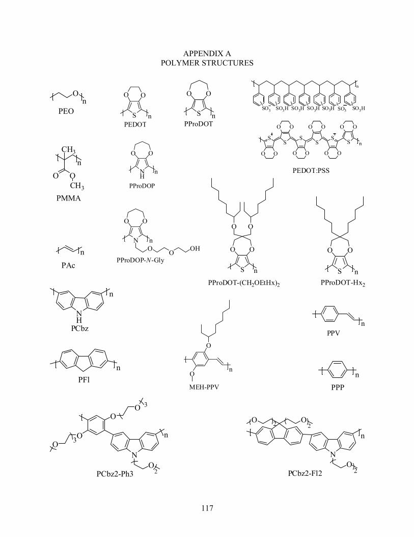
117
APPENDIX A POLYMER STRUCTURES
S
OO
nPEDOT
S
O O
S
OO
S
O O
S
OO
S
O O
S
OO
n
SO3 SO3H SO3H SO3H SO3H SO3 SO3H
n
PEDOT:PSS
S
OO
nPProDOT
nPAc
NH
OO
n
PProDOP
N
OO
O O OHn
PProDOP-N-Gly
O
O
n
MEH-PPV
S
OO
nPProDOT-Hx2
S
OO
OO
n
PProDOT-(CH2OEtHx)2
nPPV
nPPP
NH
n
PCbz
nPFl
OO
NO
22
2
n
PCbz2-Fl2
NO
O
OO
O 3
3
2
n
PCbz2-Ph3
OCH3
O
CH3
n
PMMA
On
PEO

118
LIST OF REFERENCES
1. Letheby, H. XXIX--On the production of a blue substance by the electrolysis of sulfate of
aniline; 1862; 161. 2. Natta, G.; Mazzanti, G.; Corradini, P. Atti accad. nazl. Lincei Rend. Classe sci. fis. mat. e
nat. 1958, 25, 3. 3. Watson, W. H., Jr.; McMordie, W. C., Jr.; Lands, L. G. J. Polym. Sci. 1961, 55, 137. 4. Hatano, M.; Kambara, S.; Shigeharu, O. J. Polym. Sci. 1961, 51, S26. 5. Berets, D. J.; Smith, D. S. Trans. Farad. Soc. 1968, 64, 823. 6. Kleist, F. D.; Byrd, N. R. J. Polym. Sci., Polym. Chem. Ed. 1969, 7, 3419. 7. Ito, T.; Shirakawa, H.; Ikeda, S. J. Polym. Sci., Polym. Chem. Ed. 1974, 12, 11. 8. Shirakawa, H.; Ito, T.; Ikeda, S. Makromol. Chem. 1978, 179, 1565. 9. Shirakawa, H.; Louis, E. J.; MacDiarmid, A. G.; Chiang, C. K.; Heeger, A. J. J. Chem.
Soc., Chem. Commun. 1977, 578. 10. Chiang, C. K.; Park, Y. W.; Heeger, A. J.; Shirakawa, H.; Louis, E. J.; MacDiarmid, A.
G. J. Chem. Phys. 1978, 69, 5098. 11. Chiang, C. K.; Gau, S. C.; Fincher, C. R., Jr.; Park, Y. W.; MacDiarmid, A. G.; Heeger,
A. J. Appl. Phys. Lett. 1978, 33, 18. 12. Chiang, C. K.; Druy, M. A.; Gau, S. C.; Heeger, A. J.; Louis, E. J.; MacDiarmid, A. G.;
Park, Y. W.; Shirakawa, H. J. Am. Chem. Soc. 1978, 100, 1013. 13. Reynolds, J. R.; Chien, J. C. W.; Karasz, F. E.; Lillya, C. P.; Curran, D. J. J. Phys., Coll.
1983, 171. 14. Rolland, M.; Bernier, P.; Disi, M.; Linaya, C.; Sledz, J.; Schue, F.; Fabre, J. M.; Giral, L.
J. Phys., Lett. 1980, 41, 165. 15. Nigrey, P. J.; MacDiarmid, A. G.; Heeger, A. J. J. Chem. Soc., Chem. Commun. 1979,
594. 16. Diaz, A. F.; Kanazawa, K. K.; Gardini, G. P. J. Chem. Soc., Chem. Commun. 1979, 635. 17. Kanazawa, K. K.; Diaz, A. F.; Geiss, R. H.; Gill, W. D.; Kwak, J. F.; Logan, J. A.;
Rabolt, J. F.; Street, G. B. J. Chem. Soc., Chem. Commun. 1979, 854.
119
18. Dall'Olio, A.; Dascola, G.; Varacca, V.; Bocchi, V. Comptes Rendus des Seances de l'Academie des Sciences, Serie C: Sciences Chimiques 1968, 267, 433.
19. Irvin, J. A.; Irvin, D. J.; Stenger-Smith, J. D., Electroactive Polymers for Batteries and
Supercapacitors. In Handbook of Conducting Polymers, 3 ed.; Reynolds, J. R.; Skotheim, T. A., Ed. CRC Press: Boca Raton, FL, 2006; Chapter 9.
20. Burroughes, J. H.; Bradley, D. D. C.; Brown, A. R.; Marks, R. N.; Mackay, K.; Friend, R.
H.; Burns, P. L.; Holmes, A. B. Nature 1990, 347, 539. 21. Koezuka, H.; Tsumura, A.; Ando, T. Synth. Met. 1987, 18, 699. 22. Dyer, A. L.; Reynolds, J. R., Electrochromism of Conjugated Conducting Polymers. In
Handbook of Conducting Polymers, ed.; Skotheim, T. A.; Reynolds, J. R., Ed. CRC Press: Boca Raton, FL, 2006; Chapter 20.
23. Wallace, G. G.; Dastoor, P. C.; Officer, D. L.; Too, C. O. Chemical Innovation 2000, 30,
14. 24. Smela, E. Advanced Materials 1999, 11, 1343. 25. Platt, J. R. J. Chem. Phys. 1961, 34, 862. 26. Rose, T. L.; D'Antonio, S.; Jillson, M. H.; Kon, A. B.; Suresh, R.; Wang, F. Synth. Met.
1997, 85, 1439. 27. Franke, E. B.; Trimble, C. L.; Hale, J. S.; Schubert, M.; Woollam, J. A. J. Appl. Phys.
2000, 88, 5777. 28. Topart, P.; Hourquebie, P. Thin Solid Films 1999, 352, 243. 29. Monk, P. M. S.; Mortimer, R. J.; Rosseinsky, D. R., Electrochromism: Fundamentals
and Applications. ed.; Wiley-VCH: Weinheim, Germany, 1995. 30. Deb, S. K. Appl. Opt., Suppl. 1969, No. 3, 192. 31. Deb, S. K. Philosophical Magazine 1973, 27, 801. 32. Granqvist, C. G. Electrochim. Acta 1999, 44, 3005. 33. Granqvist, C. G. Sol. Energy Mater. Sol. Cells 2000, 60, 201. 34. Mortimer, R. J. Electrochim. Acta 1999, 44, 2971. 35. Mortimer, R. J.; Reynolds, J. R. J. Mater. Chem. 2005, 15, 2226.

120
36. Garnier, F.; Tourillon, G.; Gazard, M.; Dubois, J. C. J. Electroanal. Chem. 1983, 148, 299.
37. Gazard, M.; Dubois, J. C.; Champagne, M.; Garnier, F.; Tourillon, G. J. Phys., Coll.
1983, 537. 38. Alkan, S.; Cutler, C. A.; Reynolds, J. R. Adv. Func. Mater. 2003, 13, 331. 39. Druy, M. A.; Seymour, R. J. J. Phys., Coll. 1983, 595. 40. Argun, A. A.; Cirpan, A.; Reynolds, J. R. Advanced Materials 2003, 15, 1338. 41. Groenendaal, L. B.; Jonas, F.; Freitag, D.; Pielartzik, H.; Reynolds, J. R. Advanced
Materials 2000, 12, 481. 42. Heywang, G.; Jonas, F. Advanced Materials 1992, 4, 116. 43. Cao, Y.; Yu, G.; Zhang, C.; Menon, R.; Heeger, A. J. Synth. Met. 1997, 87, 171. 44. Kirchmeyer, S.; Reuter, K. J. Mater. Chem. 2005, 15, 2077. 45. Welsh, D. M.; Kloeppner, L. J.; Madrigal, L.; Pinto, M. R.; Thompson, B. C.; Schanze,
K. S.; Abboud, K. A.; Powell, D.; Reynolds, J. R. Macromolecules 2002, 35, 6517. 46. Mishra, S. P.; Krishnamoorthy, K.; Sahoo, R.; Kumar, A. J. Polym. Sci., Part A: Polym.
Chem. 2004, 43, 419. 47. Cirpan, A.; Argun, A. A.; Grenier, C. R. G.; Reeves, B. D.; Reynolds, J. R. J. Mater.
Chem. 2003, 13, 2422. 48. Reeves, B. D.; Grenier, C. R. G.; Argun, A. A.; Cirpan, A.; McCarley, T. D.; Reynolds, J.
R. Macromolecules 2004, 37, 7559. 49. Thomas, C. A.; Zong, K.; Schottland, P.; Reynolds, J. R. Advanced Materials 2000, 12,
222. 50. Walczak, R. M.; Reynolds, J. R. Advanced Materials 2006, 18, 1121. 51. Zong, K.; Reynolds, J. R. J. Org. Chem. 2001, 66, 6873. 52. Sönmez, G.; Schwendeman, I.; Schottland, P.; Zong, K.; Reynolds, J. R. Macromolecules
2003, 36, 639. 53. Schwendeman, I.; Hickman, R.; Sönmez, G.; Schottland, P.; Zong, K.; Welsh, D. M.;
Reynolds, J. R. Chem. Mater. 2002, 14, 3118.

121
54. Gaupp, C. L.; Zong, K.; Schottland, P.; Thompson, B. C.; Thomas, C. A.; Reynolds, J. R. Macromolecules 2000, 33, 1132.
55. Schottland, P.; Zong, K.; Gaupp, C. L.; Thompson, B. C.; Thomas, C. A.; Giurgiu, I.;
Hickman, R.; Abboud, K. A.; Reynolds, J. R. Macromolecules 2000, 33, 7051. 56. Reynolds, J. R.; Zong, K.; Schwendemann, I.; Sönmez, G.; Schottland, P.; Argun, A. A.;
Aubert, P. H. Electrochromic polymers and polymer electrochromic devices. United States Patent 6,791,738, 2003.
57. Schwendeman, I.; Hwang, J.; Welsh, D. M.; Tanner, D. B.; Reynolds, J. R. Advanced
Materials 2001, 13, 634. 58. Rosseinsky, D. R.; Mortimer, R. J. Advanced Materials 2001, 13, 783. 59. Somani, P. R.; Radhakrishnan, S. Mater. Chem. Phys. 2003, 77, 117. 60. Panero, S.; Passerini, S.; Scrosati, B. Molecular Crystals and Liquid Crystals Science and
Technology, Section A: Molecular Crystals and Liquid Crystals 1993, 229, 97. 61. Argun, A. A.; Aubert, P.-H.; Thompson, B. C.; Schwendeman, I.; Gaupp, C. L.; Hwang,
J.; Pinto, N. J.; Tanner, D. B.; MacDiarmid, A. G.; Reynolds, J. R. Chem. Mater. 2004, 16, 4401.
62. Leventis, N.; Chung, Y. C. Chem. Mater. 1992, 4, 1415. 63. Granqvist, C. G.; Avendano, E.; Azens, A. Thin Solid Films 2003, 442, 201. 64. Jelle, B. P.; Hagen, G. Journal of Applied Electrochemistry 1998, 28, 1061. 65. Girotto, E. M.; De Paoli, M.-A. Advanced Materials 1998, 10, 790. 66. Shimidzu, T.; Ohtani, A.; Aiba, M.; Honda, K. Journal of the Chemical Society, Faraday
Transactions. 1 1988, 841, 3941. 67. Lu, W.; Fadeev, A. G.; Qi, B.; Smela, E.; Mattes, B. R.; Ding, J.; Spinks, G. M.;
Mazurkiewicz, J.; Zhou, D.; Wallace, G. G.; MacFarlane, D. R.; Forsyth, S. A.; Forsyth, M. Science 2002, 297, 983.
68. Vondrik, J.; Sedlaiikova, M.; Reiter, J.; Hodal, T. Electrochim. Acta 1999, 44, 3067. 69. Pawlicka, A.; Dragunski, D.; Guimaraes, K.; Avellaneda, C. Molecular Crystals and
Liquid Crystals 2004, 416, 105. 70. Lu, W.; Fadeev, A. G.; Qi, B.; Mattes, B. R. Journal of the Electrochemical Society 2004,
151, H33.
122
71. Lu, W.; Mattes, B. R.; Fadeev, A. G. Long-lived conjugated polymer electrochemical
devices incorporating ionic liquids. United States Patent 6,828,062, 2002. 72. Chandrasekhar, P.; Zay, B. J.; Birur, G. C.; Rawal, S.; Pierson, E. A.; Kauder, L.;
Swanson, T. Adv. Func. Mater. 2002, 12, 95. 73. Bennett, R. N.; Kokonaski, W. E.; Hannan, M. J.; Boxall, L. G. Electrode for display
devices. United States Patent 5,446,577, 1994. 74. Chandrasekhar, P. Electrochromic display device. United States Patent 5,995,273, 1999. 75. Argun, A. A.; Cirpan, A.; Reynolds, J. R. Advanced Materials 2003, 15, 1338. 76. Wu, Z.; Chen, Z.; Du, X.; Logan, J. M.; Sippel, J.; Nikolou, M.; Kamaras, K.; Reynolds,
J. R.; Tanner, D. B.; Hebard, A. F.; Rinzler, A. G. Science 2004, 305, 1273. 77. Brotherston, I. D.; Mudigonda, D. S. K.; Osborn, J. M.; Belk, J.; Chen, J.; Loveday, D.
C.; Boehme, J. L.; Ferraris, J. P.; Meeker, D. L. Electrochim. Acta 1999, 44, 2993. 78. Aubert, P.-H.; Argun, A. A.; Cirpan, A.; Tanner, D. B.; Reynolds, J. R. Chem. Mater.
2004, 16, 2386. 79. Argun, A. A.; Reynolds, J. R. J. Mater. Chem. 2005, 15, 1793. 80. Argun, A. A.; Berard, M.; Aubert, P.-H.; Reynolds, J. R. Advanced Materials 2005, 17,
422. 81. Tang, C. W.; VanSlyke, S. A. Appl. Phys. Lett. 1987, 51, 913. 82. Friend, R. H.; Gymer, R. W.; Holmes, A. B.; Burroughes, J. H.; Marks, R. N.; Taliani,
C.; Bradley, D. D. C.; Dos Santos, D. A.; Bredas, J. L.; Logdlund, M.; Salaneck, W. R. Nature 1999, 397, 121.
83. Fowler, R. H.; Nordheim, L. Proc. Roy. Soc. 1928, A119, 173. 84. Brown, T. M.; Cacialli, F. J. Polym. Sci., Part B: Polym. Phys. 2003, 41, 2649. 85. Kugler, T.; Salaneck, W. R.; Rost, H.; Holmes, A. B. Chem. Phys. Lett. 1999, 310, 391. 86. Parker, I. D. J. Appl. Phys. 1994, 75, 1656. 87. Campbell, I. H.; Hagler, T. W.; Smith, D. L.; Ferraris, J. P. Phys. Rev. Lett. 1996, 76,
1900. 88. Salaneck, W. R.; Bredas, J. L. Advanced Materials 1996, 8, 48.

123
89. Dannetun, P.; Logdlund, M.; Fredriksson, C.; Lazzaroni, R.; Fauquet, C.; Stafstroem, S.;
Spangler, C. W.; Bredas, J. L.; Salaneck, W. R. J. Chem. Phys. 1994, 100, 6765. 90. Gustafsson, G.; Cao, Y.; Treacy, G. M.; Klavetter, F.; Colaneri, N.; Heeger, A. J. Nature
1992, 357, 477. 91. Heeger, A. J. Solid State Commun. 1998, 107, 673. 92. Kraft, A.; Grimsdale, A. C.; Holmes, A. B. Angewandte Chemie, International Edition
1998, 37, 403. 93. Thompson, B. C.; Madrigal, L. G.; Pinto, M. R.; Kang, T.-S.; Schanze, K. S.; Reynolds,
J. R. J. Polym. Sci., Part A: Polym. Chem. 2005, 43, 1417. 94. Reddinger, J. L.; Reynolds, J. R. Macromolecules 1997, 30, 479. 95. Zhou, X.-H.; Niu, Y.-H.; Huang, F.; Liu, M. S.; Jen, A. K. Y. Macromolecules 2007, 40,
3015. 96. Zhang, Y.; Yang, J.; Hou, Q.; Mo, Y.; Peng, J.; Cao, Y. Chin. Sci. Bull. 2005, 50, 957. 97. Pei, Q.; Yu, G.; Zhang, C.; Yang, Y.; Heeger, A. J. Science 1995, 269, 1086. 98. deMello, J. C.; Halls, J. J. M.; Graham, S. C.; Tessler, N.; Friend, R. H. Phys. Rev. Lett.
2000, 85, 421. 99. Armstrong, N. R.; Wightman, R. M.; Gross, E. M. Annu. Rev. Phys. Chem. 2001, 52,
391. 100. Edman, L. Electrochim. Acta 2005, 50, 3878. 101. Gao, J.; Heeger, A. J.; Campbell, I. H.; Smith, D. L. Phys. Rev. B: Condens. Matter 1999,
59, R2482. 102. Gao, J.; Dane, J. Appl. Phys. Lett. 2004, 84, 2778. 103. Dick, D. J.; Heeger, A. J.; Yang, Y.; Pei, Q. Advanced Materials 1996, 8, 985. 104. Edman, L.; Summers, M. A.; Buratto, S. K.; Heeger, A. J. Phys. Rev. B: Condens. Matter
2004, 70, 115212/1. 105. Holzer, L.; Wenzl, F. P.; Sotgiu, R.; Gritsch, M.; Tasch, S.; Hutter, H.; Sampietro, M.;
Leising, G. Synth. Met. 1999, 102, 1022. 106. Manzanares, J. A.; Reiss, H.; Heeger, A. J. J. Phys. Chem. B 1998, 102, 4327.
124
107. Neher, D.; Gruner, J.; Cimrova, V.; Schmidt, W.; Rulkens, R.; Lauter, U. Polym. Adv.
Tech. 1998, 9, 461. 108. Pei, Q.; Yang, Y. Synth. Met. 1996, 80, 131. 109. Pei, Q.; Yang, Y.; Yu, G.; Zhang, C.; Heeger, A. J. Journal of the American Chemical
Society 1996, 118, 3922. 110. Smith, D. L. J. Appl. Phys. 1997, 81, 2869. 111. Xu, Z.; Liu, M.; Chen, X.; Hou, Y.; Teng, F.; Meng, L.; Xu, X. Displays 2006, 27, 45. 112. Cao, Y.; Yu, G.; Heeger, A. J.; Yang, C. Y. Appl. Phys. Lett. 1996, 68, 3218. 113. Ryan, A. J. Nature Materials 2002, 1, 8. 114. Wenzl, F. P.; Pachler, P.; Suess, C.; Haase, A.; List, E. J. W.; Poelt, P.; Somitsch, D.;
Knoll, P.; Scherf, U.; Leising, G. Adv. Func. Mater. 2004, 14, 441. 115. Cao, Y.; Pei, Q.; Andersson, M. R.; Yu, G.; Heeger, A. J. Journal of the Electrochemical
Society 1997, 144, 317. 116. Edman, L.; Pauchard, M.; Liu, B.; Bazan, G.; Moses, D.; Heeger, A. J. Appl. Phys. Lett.
2003, 82, 3961. 117. Kong, F.; Zhang, S. Y.; Zheng, Y.; Ou, C. G.; Yang, C. Z.; Yuan, R. K. J. Appl. Polym.
Sci. 2006, 101, 4253. 118. Wenzl, F. P.; Poelt, P.; Haase, A.; Patil, S.; Scherf, U.; Leising, G. Solid State Ionics
2005, 176, 1747. 119. Pachler, P.; Wenzl, F. P.; Scherf, U.; Leising, G. J. Phys. Chem. B 2005, 109, 6020. 120. Yang, C.; Sun, Q.; Qiao, J.; Li, Y. J. Phys. Chem. B 2003, 107, 12981. 121. Sun, Q.; Wang, H.; Yang, C.; Li, Y. Synth. Met. 2003, 137, 1087. 122. Sun, Q. J.; Wang, H. Q.; Yang, C. H.; Wang, X. G.; Liu, D. S.; Li, Y. F. Thin Solid Films
2002, 417, 14. 123. Yang, Y.; Pei, Q. J. Appl. Phys. 1997, 81, 3294. 124. Holzer, L.; Winkler, B.; Wenzl, F. P.; Tasch, S.; Dai, L.; Mau, A. W. H.; Leising, G.
Synth. Met. 1999, 100, 71.
125
125. Morgado, J.; Cacialli, F.; Friend, R. H.; Chuah, B. S.; Rost, H.; Holmes, A. B. Macromolecules 2001, 34, 3094.
126. Morgado, J.; Friend, R. H.; Cacialli, F.; Chuah, B. S.; Rost, H.; Moratti, S. C.; Holmes,
A. B. Synth. Met. 2001, 122, 111. 127. Gao, J.; Dane, J. Appl. Phys. Lett. 2003, 83, 3027. 128. Leger, J. M.; Carter, S. A.; Ruhstaller, B. J. Appl. Phys. 2005, 98, 1. 129. Shin, J.-H.; Edman, L. J. Am. Chem. Soc. 2006, 128, 15568. 130. Shin, J. H.; Matyba, P.; Robinson, N. D.; Edman, L. Electrochim. Acta 2007, 52, 6456. 131. Andersson, P.; Nilsson, D.; Svensson, P.-O.; Chen, M.; Malmstrom, A.; Remonen, T.;
Kugler, T.; Berggren, M. Advanced Materials 2002, 14, 1460. 132. Cravino, A.; Leriche, P.; Aleveque, O.; Roquet, S.; Roncali, J. Advanced Materials 2006,
18, 3033. 133. Kim, H.; Kim, J. Y.; Park, S. H.; Lee, K.; Jin, Y.; Kim, J.; Suh, H. Appl. Phys. Lett. 2005,
86, 1. 134. Yang, C.-J.; Cho, T.-Y.; Lin, C.-L.; Wu, C.-C. Appl. Phys. Lett. 2007, 90, 1. 135. Yang, C.-Y.; Cho, T.-Y.; Chen, Y.-Y.; Yang, C.-J.; Meng, C.-Y.; Yang, C.-H.; Yang, P.-
C.; Chang, H.-Y.; Hsueh, C.-Y.; Wu, C.-C.; Lee, S.-C. Appl. Phys. Lett. 2007, 90, 1. 136. Wang, X. J.; Lau, W. M.; Wong, K. Y. Appl. Phys. Lett. 2005, 87, 1. 137. Johansson, T.; Persson, N.-K.; Inganaes, O. Journal of the Electrochemical Society 2004,
151, E119. 138. Lacroix, J. C.; Fraoua, K.; Lacaze, P. C. Journal of Electroanalytical Chemistry 1998,
444, 83. 139. Aoki, K.; Cao, J.; Hoshino, Y. Electrochim. Acta 1993, 38, 1711. 140. Aoki, K.; Teragishi, Y. Journal of Electroanalytical Chemistry 1998, 441, 25. 141. Tezuka, Y.; Aoki, K. Journal of Electroanalytical Chemistry 1989, 273, 161. 142. Tezuka, Y.; Aoki, K.; Yajima, H.; Ishii, T. Journal of Electroanalytical Chemistry 1997,
425, 167.
126
143. Tezuka, Y.; Kimura, T.; Ishii, T.; Aoki, K. Journal of Electroanalytical Chemistry 1995, 395, 51.
144. Wemple, S. H.; Seman, J. A. Applied Optics 1973, 12, 2947. 145. Cohen, S. Laser Focus World 2000, 36, 139. 146. O'Brien, N. A.; Mathew, J. G. H.; Cumbo, M. J.; Hichwa, B. P.; Adair, R. W. Variable
optical attenuator device. United States Patent 6,625,378, 2003. 147. Sato, K.; Aoki, T.; Watanabe, Y.; Oguri, Y.; Shibata, N.; Nishiwaki, T.; Oike, M.; Ota, T.
Furukawa Review 2001, 20, 15. 148. Uetsuka, H.; Hasegawa, T.; Ohkawa, M.; Takasugi, S.; Kitano, N.; Tanaka, K. Hitachi
Cable Review 2001, 20, 15. 149. Pan, J.-J. Polarization-independent optical switch/attenuator. United States Patent
5,276,747, 1994. 150. Loukina, T.; Chevallier, R.; de Bougrenet de la Tocnaye, J. L.; Barge, M. J. Lightwave
Technol. 2003, 21, 2067. 151. Khalil, D.; Maaty, H.; Bashir, A.; Saadany, B. Microw. Optic. Tech. Lett. 2003, 36, 110. 152. Morimoto, M.; Morimoto, K.; Sato, K.; Iizuka, S. i. Furukawa Review 2003, 23, 26. 153. Liu, A. Q.; Zhang, X. M.; Lu, C.; Wang, F.; Lu, C.; Liu, Z. S. J. Micromech. Microeng.
2003, 13, 400. 154. Barber, B.; Giles, C. R.; Askyuk, V.; Ruel, R.; Stulz, L.; Bishop, D. IEEE Photonics
Technology Letters 1998, 10, 1262. 155. Ford, J. E.; Walker, J. A.; Greywall, D. S.; Goossen, K. W. J. Lightwave Technol. 1998,
16, 1663. 156. Cowin, M. A.; Varrazza, R.; Morgan, C.; Penty, R. V.; White, I. H.; McDonagh, A. M.;
Bayly, S.; Riley, J.; Ward, M. D.; McCleverty, J. A. Trends in Optics and Photonics 2001, 54, WR6/1.
157. Franke, E. B.; Trimble, C. L.; Hale, J. S.; Schubert, M.; Woollam, J. A. J. Appl. Phys.
2000, 88, 5777. 158. MacPherson, C. D.; Anderson, K.; McGarry, S. P. Electrochromic optical attenuator. U.S.
Patent Appl. US 2002/0067905 A1, 2002.
127
159. McDonagh, A. M.; Bayly, S. R.; Riley, D. J.; Ward, M. D.; McCleverty, J. A.; Cowin, M. A.; Morgan, C. N.; Varrazza, R.; Penty, R. V.; White, I. H. Chem. Mater. 2000, 12, 2523.
160. Qi, Y.; Wang, Z. Y. Macromolecules 2003, 36, 3146. 161. Qi, Y. H.; Desjardins, P.; Meng, X. S.; Wang, Z. Y. Optic. Mater. 2002, 21, 255. 162. Qi, Y.-h.; Desjardins, P.; Birau, M.; Wu, X.-g.; Wang, Z.-y. Chin. J. Polym. Sci. 2003,
21, 147. 163. Vergaz, R.; Barrios, D.; Sánchez-Pena, J. M.; Vázquez, C.; Pozo-Gonzalo, C.;
Mecerreyes, D.; Pomposo, J. Proceedings of SPIE: Photonic materials, devices, and applications 2005, 5840, 389.
164. Wang, Z. Y.; Zhang, J. D.; Wu, X. G.; Birau, M.; Yu, G.; Yu, H. A.; Qi, Y.; Desjardins,
P.; Meng, X. S.; Gao, J. P.; Todd, E.; Song, N.; Bai, Y.; Beaudin, A. M. R.; LeClair, G. Pure Appl. Chem. 2004, 76, 1435.
165. Ward, M. D. Journal of Solid State Electrochemistry 2005, 9, 778. 166. Zhang, J. D.; Lu, F.; Huang, H.; Wang, J.; Yu, H. a.; Jiang, J.; Yan, D.; Wang, Z. Synth.
Met. 2005, 148, 123. 167. Zhang, J. D.; Yu, H. A.; Wu, X. G.; Wang, Z. Y. Optic. Mater. 2004, 27, 265. 168. Groenendaal, L. B.; Zotti, G.; Aubert, P.-H.; Waybright, S. M.; Reynolds, J. R. Advanced
Materials 2003, 15, 855. 169. Xia, C.; Advincula, R. C. Macromolecules 2001, 34, 5854. 170. de Leeuw, D. M.; Simenon, M. M. J.; Brown, A. R.; Einerhand, R. E. F. Synth. Met.
1997, 87, 53. 171. Santos, L. F.; Faria, R. C.; Gaffo, L.; Carvalho, L. M.; Faria, R. M.; Gonc¸alves, D.
Electrochim. Acta 2007, 52, 4299. 172. Zhong, Z. Y.; Jiang, Y. D. European Physical Journal: Applied Physics 2006, 34, 173. 173. Wu, C. C.; Wu, C. I.; Sturm, J. C.; Kahn, A. Appl. Phys. Lett. 1997, 70, 1348. 174. Quintens, D.; Muys, B.; Van Thillo, E.; Samijn, R. Antistatic coating on hydrophobic
resin or paper support. U. S. Patent 5,354,613, 1994. 175. Kawamoto, H. Proceedings of the IEEE 2002, 90, 460. 176. IMOD Technology Overview; QUALCOMM Inc.: 2007.

128
177. Reader from Sony. http://www.learningcenter.sony.us/assets/itpd/reader/ (November 3,
2007), 178. Motorola MOTOFONE.
http://www.motorola.com/motoinfo/product/details.jsp?globalObjectId=164 (November 3, 2007),
179. Cecchi, M.; Smith, H.; Braun, D. Synth. Met. 2001, 121, 1715. 180. McCluney, R., Introduction to Radiometry and Photometry. ed.; Artech House, Inc:
Norwood, MA, 1994. 181. Kaufman, J. E., ed., IES Lighting Handbook-Reference Volume. ed.; Illuminating
Engineering Society of North America: New York, NY, 1984. 182. Edman, L.; Moses, D.; Heeger, A. J. Synth. Met. 2003, 138, 441. 183. Ratner, M. A.; Shriver, D. F. Chemical Reviews 1988, 88, 109. 184. Trotzig, C.; Abrahmsén-Alami, S.; Maurer, F. H. J. Polymer 2007, 48, 3294. 185. Shin, J.-H.; Edman, L. Journal of the American Chemical Society 2006, 128, 15568. 186. Argun, A. A.; Cirpan, A.; Reynolds, J. R. Advanced Materials (Weinheim, Germany)
2003, 15, 1338. 187. Brookins, R. N., Synthesis and Characterization of Carbazole-Based Conjugated
Polymers for Electrochromic/Electroluminescent Applications. In University of Florida: 2005.
188. Ananthakrishnan, N. Morphology effects on the light emitting properties of conjugated
polymer blends. Dissertation, University of Florida, Gainesville, 2005. 189. Schwendeman, I. Optical and transport properties of conjugated polymers and their
application to electrochromic devices. Dissertation, University of Florida, Gainesville, 2002.
190. Thomas, C. A. Donor-acceptor methods for band gap reduction in conjugated polymers:
the role of electron rich donor heterocycles. Dissertation, University of Florida, Gainesville, 2002.

129
BIOGRAPHICAL SKETCH
Aubrey Lynn Dedrickson was born July 13, 1978 in Bataan, Philippines to Sheila and
Randy Dedrickson. Her father was in the U.S. Navy, and therefore her family moved around
quite a bit. They lived in Homestead, FL, Hawaii, Pensacola, FL, and Altamonte Springs, FL.
She has one younger brother, Shaun Dedrickson, and one younger sister, Stephanie Dedrickson.
She graduated high school in Pensacola, FL after which she attended the University of West
Florida for her first year of college while working full-time. She and Nathan Dyer married in
1999 in Pensacola, Florida and they both moved to Shippensburg, PA where Aubrey attended
Shippensburg University of Pennsylvania full-time. She received her B.S. in Chemistry in the
Summer of 2002 and began her graduate studies at the University of Florida that August. In the
Fall of 2002, she joined the Reynolds research group.