connectivity line, arm®-based 32-bit mcu with 64/256 kb
TRANSCRIPT

This is information on a product in full production.
September 2015 DocID15274 Rev 9 1/107
STM32F105xxSTM32F107xx
Connectivity line, ARM®-based 32-bit MCU with 64/256 KB Flash, USBOTG, Ethernet, 10 timers, 2 CANs, 2 ADCs, 14 communication interfaces
Datasheet - production data
Features
• Core: ARM® 32-bit Cortex®-M3 CPU
– 72 MHz maximum frequency, 1.25 DMIPS/MHz (Dhrystone 2.1) performance at 0 wait state memory access
– Single-cycle multiplication and hardware division
• Memories
– 64 to 256 Kbytes of Flash memory
– 64 Kbytes of general-purpose SRAM
• Clock, reset and supply management
– 2.0 to 3.6 V application supply and I/Os
– POR, PDR, and programmable voltage detector (PVD)
– 3-to-25 MHz crystal oscillator
– Internal 8 MHz factory-trimmed RC
– Internal 40 kHz RC with calibration
– 32 kHz oscillator for RTC with calibration
• Low power
– Sleep, Stop and Standby modes
– VBAT supply for RTC and backup registers
• 2 × 12-bit, 1 µs A/D converters (16 channels)
– Conversion range: 0 to 3.6 V
– Sample and hold capability
– Temperature sensor
– up to 2 MSPS in interleaved mode
• 2 × 12-bit D/A converters
• DMA: 12-channel DMA controller
– Supported peripherals: timers, ADCs, DAC, I2Ss, SPIs, I2Cs and USARTs
• Debug mode
– Serial wire debug (SWD) & JTAG interfaces
– Cortex®-M3 Embedded Trace Macrocell™
• Up to 80 fast I/O ports
– 51/80 I/Os, all mappable on 16 external interrupt vectors and almost all 5 V-tolerant
• CRC calculation unit, 96-bit unique ID
• Up to 10 timers with pinout remap capability
– Up to four 16-bit timers, each with up to 4 IC/OC/PWM or pulse counter and quadrature (incremental) encoder input
– 1 × 16-bit motor control PWM timer with dead-time generation and emergency stop
– 2 × watchdog timers (Independent and Window)
– SysTick timer: a 24-bit downcounter
– 2 × 16-bit basic timers to drive the DAC
• Up to 14 communication interfaces with pinout remap capability
– Up to 2 × I2C interfaces (SMBus/PMBus)
– Up to 5 USARTs (ISO 7816 interface, LIN, IrDA capability, modem control)
– Up to 3 SPIs (18 Mbit/s), 2 with a multiplexed I2S interface that offers audio class accuracy via advanced PLL schemes
– 2 × CAN interfaces (2.0B Active) with 512 bytes of dedicated SRAM
– USB 2.0 full-speed device/host/OTG controller with on-chip PHY that supports HNP/SRP/ID with 1.25 Kbytes of dedicated SRAM
– 10/100 Ethernet MAC with dedicated DMA and SRAM (4 Kbytes): IEEE1588 hardware support, MII/RMII available on all packages
Table 1. Device summary
Reference Part number
STM32F105xxSTM32F105R8, STM32F105V8 STM32F105RB, STM32F105VB STM32F105RC, STM32F105VC
STM32F107xxSTM32F107RB, STM32F107VB STM32F107RC, STM32F107VC
LQFP100 14 × 14 mmLQFP64 10 × 10 mm
FBGA
LFBGA100 10 × 10 mm
www.st.com

Contents STM32F105xx, STM32F107xx
2/107 DocID15274 Rev 9
Contents
1 Introduction . . . . . . . . . . . . . . . . . . . . . . . . . . . . . . . . . . . . . . . . . . . . . . . . 9
2 Description . . . . . . . . . . . . . . . . . . . . . . . . . . . . . . . . . . . . . . . . . . . . . . . . 10
2.1 Device overview . . . . . . . . . . . . . . . . . . . . . . . . . . . . . . . . . . . . . . . . . . . . 10
2.2 Full compatibility throughout the family . . . . . . . . . . . . . . . . . . . . . . . . . . 12
2.3 Overview . . . . . . . . . . . . . . . . . . . . . . . . . . . . . . . . . . . . . . . . . . . . . . . . . 13
2.3.1 ARM Cortex-M3 core with embedded Flash and SRAM . . . . . . . . . . . . 14
2.3.2 Embedded Flash memory . . . . . . . . . . . . . . . . . . . . . . . . . . . . . . . . . . . 14
2.3.3 CRC (cyclic redundancy check) calculation unit . . . . . . . . . . . . . . . . . . 14
2.3.4 Embedded SRAM . . . . . . . . . . . . . . . . . . . . . . . . . . . . . . . . . . . . . . . . . 14
2.3.5 Nested vectored interrupt controller (NVIC) . . . . . . . . . . . . . . . . . . . . . . 14
2.3.6 External interrupt/event controller (EXTI) . . . . . . . . . . . . . . . . . . . . . . . 15
2.3.7 Clocks and startup . . . . . . . . . . . . . . . . . . . . . . . . . . . . . . . . . . . . . . . . . 15
2.3.8 Boot modes . . . . . . . . . . . . . . . . . . . . . . . . . . . . . . . . . . . . . . . . . . . . . . 15
2.3.9 Power supply schemes . . . . . . . . . . . . . . . . . . . . . . . . . . . . . . . . . . . . . 16
2.3.10 Power supply supervisor . . . . . . . . . . . . . . . . . . . . . . . . . . . . . . . . . . . . 16
2.3.11 Voltage regulator . . . . . . . . . . . . . . . . . . . . . . . . . . . . . . . . . . . . . . . . . . 16
2.3.12 Low-power modes . . . . . . . . . . . . . . . . . . . . . . . . . . . . . . . . . . . . . . . . . 16
2.3.13 DMA . . . . . . . . . . . . . . . . . . . . . . . . . . . . . . . . . . . . . . . . . . . . . . . . . . . . 17
2.3.14 RTC (real-time clock) and backup registers . . . . . . . . . . . . . . . . . . . . . . 17
2.3.15 Timers and watchdogs . . . . . . . . . . . . . . . . . . . . . . . . . . . . . . . . . . . . . . 18
2.3.16 I²C bus . . . . . . . . . . . . . . . . . . . . . . . . . . . . . . . . . . . . . . . . . . . . . . . . . . 19
2.3.17 Universal synchronous/asynchronous receiver transmitters (USARTs) . 19
2.3.18 Serial peripheral interface (SPI) . . . . . . . . . . . . . . . . . . . . . . . . . . . . . . . 20
2.3.19 Inter-integrated sound (I2S) . . . . . . . . . . . . . . . . . . . . . . . . . . . . . . . . . . 20
2.3.20 Ethernet MAC interface with dedicated DMA and IEEE 1588 support . 20
2.3.21 Controller area network (CAN) . . . . . . . . . . . . . . . . . . . . . . . . . . . . . . . 21
2.3.22 Universal serial bus on-the-go full-speed (USB OTG FS) . . . . . . . . . . . 21
2.3.23 GPIOs (general-purpose inputs/outputs) . . . . . . . . . . . . . . . . . . . . . . . . 21
2.3.24 Remap capability . . . . . . . . . . . . . . . . . . . . . . . . . . . . . . . . . . . . . . . . . . 22
2.3.25 ADCs (analog-to-digital converters) . . . . . . . . . . . . . . . . . . . . . . . . . . . . 22
2.3.26 DAC (digital-to-analog converter) . . . . . . . . . . . . . . . . . . . . . . . . . . . . . 22
2.3.27 Temperature sensor . . . . . . . . . . . . . . . . . . . . . . . . . . . . . . . . . . . . . . . . 23
2.3.28 Serial wire JTAG debug port (SWJ-DP) . . . . . . . . . . . . . . . . . . . . . . . . . 23
DocID15274 Rev 9 3/107
STM32F105xx, STM32F107xx Contents
4
2.3.29 Embedded Trace Macrocell™ . . . . . . . . . . . . . . . . . . . . . . . . . . . . . . . . 23
3 Pinouts and pin description . . . . . . . . . . . . . . . . . . . . . . . . . . . . . . . . . . 24
4 Memory mapping . . . . . . . . . . . . . . . . . . . . . . . . . . . . . . . . . . . . . . . . . . . 33
5 Electrical characteristics . . . . . . . . . . . . . . . . . . . . . . . . . . . . . . . . . . . . 34
5.1 Parameter conditions . . . . . . . . . . . . . . . . . . . . . . . . . . . . . . . . . . . . . . . . 34
5.1.1 Minimum and maximum values . . . . . . . . . . . . . . . . . . . . . . . . . . . . . . . 34
5.1.2 Typical values . . . . . . . . . . . . . . . . . . . . . . . . . . . . . . . . . . . . . . . . . . . . 34
5.1.3 Typical curves . . . . . . . . . . . . . . . . . . . . . . . . . . . . . . . . . . . . . . . . . . . . 34
5.1.4 Loading capacitor . . . . . . . . . . . . . . . . . . . . . . . . . . . . . . . . . . . . . . . . . 34
5.1.5 Pin input voltage . . . . . . . . . . . . . . . . . . . . . . . . . . . . . . . . . . . . . . . . . . 34
5.1.6 Power supply scheme . . . . . . . . . . . . . . . . . . . . . . . . . . . . . . . . . . . . . . 35
5.1.7 Current consumption measurement . . . . . . . . . . . . . . . . . . . . . . . . . . . 35
5.2 Absolute maximum ratings . . . . . . . . . . . . . . . . . . . . . . . . . . . . . . . . . . . . 36
5.3 Operating conditions . . . . . . . . . . . . . . . . . . . . . . . . . . . . . . . . . . . . . . . . 37
5.3.1 General operating conditions . . . . . . . . . . . . . . . . . . . . . . . . . . . . . . . . . 37
5.3.2 Operating conditions at power-up / power-down . . . . . . . . . . . . . . . . . . 38
5.3.3 Embedded reset and power control block characteristics . . . . . . . . . . . 38
5.3.4 Embedded reference voltage . . . . . . . . . . . . . . . . . . . . . . . . . . . . . . . . . 39
5.3.5 Supply current characteristics . . . . . . . . . . . . . . . . . . . . . . . . . . . . . . . . 39
5.3.6 External clock source characteristics . . . . . . . . . . . . . . . . . . . . . . . . . . . 47
5.3.7 Internal clock source characteristics . . . . . . . . . . . . . . . . . . . . . . . . . . . 52
5.3.8 PLL, PLL2 and PLL3 characteristics . . . . . . . . . . . . . . . . . . . . . . . . . . . 53
5.3.9 Memory characteristics . . . . . . . . . . . . . . . . . . . . . . . . . . . . . . . . . . . . . 54
5.3.10 EMC characteristics . . . . . . . . . . . . . . . . . . . . . . . . . . . . . . . . . . . . . . . . 54
5.3.11 Absolute maximum ratings (electrical sensitivity) . . . . . . . . . . . . . . . . . 56
5.3.12 I/O current injection characteristics . . . . . . . . . . . . . . . . . . . . . . . . . . . . 56
5.3.13 I/O port characteristics . . . . . . . . . . . . . . . . . . . . . . . . . . . . . . . . . . . . . . 57
5.3.14 NRST pin characteristics . . . . . . . . . . . . . . . . . . . . . . . . . . . . . . . . . . . . 62
5.3.15 TIM timer characteristics . . . . . . . . . . . . . . . . . . . . . . . . . . . . . . . . . . . . 63
5.3.16 Communications interfaces . . . . . . . . . . . . . . . . . . . . . . . . . . . . . . . . . . 64
5.3.17 12-bit ADC characteristics . . . . . . . . . . . . . . . . . . . . . . . . . . . . . . . . . . . 74
5.3.18 DAC electrical specifications . . . . . . . . . . . . . . . . . . . . . . . . . . . . . . . . . 79
5.3.19 Temperature sensor characteristics . . . . . . . . . . . . . . . . . . . . . . . . . . . . 81

Contents STM32F105xx, STM32F107xx
4/107 DocID15274 Rev 9
6 Package characteristics . . . . . . . . . . . . . . . . . . . . . . . . . . . . . . . . . . . . . 82
6.1 Package mechanical data . . . . . . . . . . . . . . . . . . . . . . . . . . . . . . . . . . . . 82
6.2 Thermal characteristics . . . . . . . . . . . . . . . . . . . . . . . . . . . . . . . . . . . . . . 90
6.2.1 Reference document . . . . . . . . . . . . . . . . . . . . . . . . . . . . . . . . . . . . . . . 90
6.2.2 Selecting the product temperature range . . . . . . . . . . . . . . . . . . . . . . . 91
7 Part numbering . . . . . . . . . . . . . . . . . . . . . . . . . . . . . . . . . . . . . . . . . . . . 93
Appendix A Application block diagrams . . . . . . . . . . . . . . . . . . . . . . . . . . . . . . . 94
A.1 USB OTG FS interface solutions. . . . . . . . . . . . . . . . . . . . . . . . . . . . . . . . 94
A.2 Ethernet interface solutions. . . . . . . . . . . . . . . . . . . . . . . . . . . . . . . . . . . . 96
A.3 Complete audio player solutions . . . . . . . . . . . . . . . . . . . . . . . . . . . . . . . . 98
A.4 USB OTG FS interface + Ethernet/I2S interface solutions . . . . . . . . . . . . 99
8 Revision history . . . . . . . . . . . . . . . . . . . . . . . . . . . . . . . . . . . . . . . . . . 102

DocID15274 Rev 9 5/107
STM32F105xx, STM32F107xx List of tables
6
List of tables
Table 1. Device summary . . . . . . . . . . . . . . . . . . . . . . . . . . . . . . . . . . . . . . . . . . . . . . . . . . . . . . . . . . 1Table 2. STM32F105xx and STM32F107xx features and peripheral counts . . . . . . . . . . . . . . . . . . 10Table 3. STM32F105xx and STM32F107xx family versus STM32F103xx family . . . . . . . . . . . . . . 12Table 4. Timer feature comparison. . . . . . . . . . . . . . . . . . . . . . . . . . . . . . . . . . . . . . . . . . . . . . . . . . 18Table 5. Pin definitions . . . . . . . . . . . . . . . . . . . . . . . . . . . . . . . . . . . . . . . . . . . . . . . . . . . . . . . . . . . 27Table 6. Voltage characteristics . . . . . . . . . . . . . . . . . . . . . . . . . . . . . . . . . . . . . . . . . . . . . . . . . . . . 36Table 7. Current characteristics . . . . . . . . . . . . . . . . . . . . . . . . . . . . . . . . . . . . . . . . . . . . . . . . . . . . 36Table 8. Thermal characteristics. . . . . . . . . . . . . . . . . . . . . . . . . . . . . . . . . . . . . . . . . . . . . . . . . . . . 37Table 9. General operating conditions . . . . . . . . . . . . . . . . . . . . . . . . . . . . . . . . . . . . . . . . . . . . . . . 37Table 10. Operating condition at power-up / power down . . . . . . . . . . . . . . . . . . . . . . . . . . . . . . . . . 38Table 11. Embedded reset and power control block characteristics. . . . . . . . . . . . . . . . . . . . . . . . . . 38Table 12. Embedded internal reference voltage. . . . . . . . . . . . . . . . . . . . . . . . . . . . . . . . . . . . . . . . . 39Table 13. Maximum current consumption in Run mode, code with data processing
running from Flash . . . . . . . . . . . . . . . . . . . . . . . . . . . . . . . . . . . . . . . . . . . . . . . . . . . . . . . 40Table 14. Maximum current consumption in Run mode, code with data processing
running from RAM. . . . . . . . . . . . . . . . . . . . . . . . . . . . . . . . . . . . . . . . . . . . . . . . . . . . . . . . 40Table 15. Maximum current consumption in Sleep mode, code running from Flash or RAM. . . . . . . 41Table 16. Typical and maximum current consumptions in Stop and Standby modes . . . . . . . . . . . . 41Table 17. Typical current consumption in Run mode, code with data processing
running from Flash . . . . . . . . . . . . . . . . . . . . . . . . . . . . . . . . . . . . . . . . . . . . . . . . . . . . . . . 44Table 18. Typical current consumption in Sleep mode, code running from Flash or
RAM . . . . . . . . . . . . . . . . . . . . . . . . . . . . . . . . . . . . . . . . . . . . . . . . . . . . . . . . . . . . . . . . . . 45Table 19. Peripheral current consumption . . . . . . . . . . . . . . . . . . . . . . . . . . . . . . . . . . . . . . . . . . . . . 46Table 20. High-speed external user clock characteristics. . . . . . . . . . . . . . . . . . . . . . . . . . . . . . . . . . 47Table 21. Low-speed external user clock characteristics . . . . . . . . . . . . . . . . . . . . . . . . . . . . . . . . . . 48Table 22. HSE 3-25 MHz oscillator characteristics . . . . . . . . . . . . . . . . . . . . . . . . . . . . . . . . . . . . . . 49Table 23. LSE oscillator characteristics (fLSE = 32.768 kHz) . . . . . . . . . . . . . . . . . . . . . . . . . . . . . . . 50Table 24. HSI oscillator characteristics . . . . . . . . . . . . . . . . . . . . . . . . . . . . . . . . . . . . . . . . . . . . . . . 52Table 25. LSI oscillator characteristics . . . . . . . . . . . . . . . . . . . . . . . . . . . . . . . . . . . . . . . . . . . . . . . 52Table 26. Low-power mode wakeup timings . . . . . . . . . . . . . . . . . . . . . . . . . . . . . . . . . . . . . . . . . . . 53Table 27. PLL characteristics . . . . . . . . . . . . . . . . . . . . . . . . . . . . . . . . . . . . . . . . . . . . . . . . . . . . . . . 53Table 28. PLL2 and PLL3 characteristics . . . . . . . . . . . . . . . . . . . . . . . . . . . . . . . . . . . . . . . . . . . . . . 53Table 29. Flash memory characteristics . . . . . . . . . . . . . . . . . . . . . . . . . . . . . . . . . . . . . . . . . . . . . . . 54Table 30. Flash memory endurance and data retention . . . . . . . . . . . . . . . . . . . . . . . . . . . . . . . . . . . 54Table 31. EMS characteristics . . . . . . . . . . . . . . . . . . . . . . . . . . . . . . . . . . . . . . . . . . . . . . . . . . . . . . 55Table 32. EMI characteristics . . . . . . . . . . . . . . . . . . . . . . . . . . . . . . . . . . . . . . . . . . . . . . . . . . . . . . . 56Table 33. ESD absolute maximum ratings . . . . . . . . . . . . . . . . . . . . . . . . . . . . . . . . . . . . . . . . . . . . . 56Table 34. Electrical sensitivities . . . . . . . . . . . . . . . . . . . . . . . . . . . . . . . . . . . . . . . . . . . . . . . . . . . . . 56Table 35. I/O current injection susceptibility . . . . . . . . . . . . . . . . . . . . . . . . . . . . . . . . . . . . . . . . . . . . 57Table 36. I/O static characteristics . . . . . . . . . . . . . . . . . . . . . . . . . . . . . . . . . . . . . . . . . . . . . . . . . . . 57Table 37. Output voltage characteristics . . . . . . . . . . . . . . . . . . . . . . . . . . . . . . . . . . . . . . . . . . . . . . 60Table 38. I/O AC characteristics . . . . . . . . . . . . . . . . . . . . . . . . . . . . . . . . . . . . . . . . . . . . . . . . . . . . . 61Table 39. NRST pin characteristics . . . . . . . . . . . . . . . . . . . . . . . . . . . . . . . . . . . . . . . . . . . . . . . . . . 62Table 40. TIMx characteristics . . . . . . . . . . . . . . . . . . . . . . . . . . . . . . . . . . . . . . . . . . . . . . . . . . . . . . 63Table 41. I2C characteristics. . . . . . . . . . . . . . . . . . . . . . . . . . . . . . . . . . . . . . . . . . . . . . . . . . . . . . . . 64Table 42. SCL frequency (fPCLK1= 36 MHz.,VDD = 3.3 V) . . . . . . . . . . . . . . . . . . . . . . . . . . . . . . . . . 65Table 43. SPI characteristics . . . . . . . . . . . . . . . . . . . . . . . . . . . . . . . . . . . . . . . . . . . . . . . . . . . . . . . 66Table 44. I2S characteristics. . . . . . . . . . . . . . . . . . . . . . . . . . . . . . . . . . . . . . . . . . . . . . . . . . . . . . . . 69

List of tables STM32F105xx, STM32F107xx
6/107 DocID15274 Rev 9
Table 45. USB OTG FS startup time . . . . . . . . . . . . . . . . . . . . . . . . . . . . . . . . . . . . . . . . . . . . . . . . . 71Table 46. USB OTG FS DC electrical characteristics. . . . . . . . . . . . . . . . . . . . . . . . . . . . . . . . . . . . . 71Table 47. USB OTG FS electrical characteristics . . . . . . . . . . . . . . . . . . . . . . . . . . . . . . . . . . . . . . . . 72Table 48. Ethernet DC electrical characteristics . . . . . . . . . . . . . . . . . . . . . . . . . . . . . . . . . . . . . . . . . 72Table 49. Dynamic characteristics: Ethernet MAC signals for SMI. . . . . . . . . . . . . . . . . . . . . . . . . . . 72Table 50. Dynamic characteristics: Ethernet MAC signals for RMII . . . . . . . . . . . . . . . . . . . . . . . . . . 73Table 51. Dynamic characteristics: Ethernet MAC signals for MII . . . . . . . . . . . . . . . . . . . . . . . . . . . 74Table 52. ADC characteristics . . . . . . . . . . . . . . . . . . . . . . . . . . . . . . . . . . . . . . . . . . . . . . . . . . . . . . 74Table 53. RAIN max for fADC = 14 MHz. . . . . . . . . . . . . . . . . . . . . . . . . . . . . . . . . . . . . . . . . . . . . . . . 75Table 54. ADC accuracy - limited test conditions . . . . . . . . . . . . . . . . . . . . . . . . . . . . . . . . . . . . . . . . 76Table 55. ADC accuracy . . . . . . . . . . . . . . . . . . . . . . . . . . . . . . . . . . . . . . . . . . . . . . . . . . . . . . . . . . 76Table 56. DAC characteristics . . . . . . . . . . . . . . . . . . . . . . . . . . . . . . . . . . . . . . . . . . . . . . . . . . . . . . 79Table 57. TS characteristics . . . . . . . . . . . . . . . . . . . . . . . . . . . . . . . . . . . . . . . . . . . . . . . . . . . . . . . . 81Table 58. LFBGA100 recommended PCB design rules (0.8 mm pitch BGA). . . . . . . . . . . . . . . . . . . 83Table 59. LQPF100 - 100-pin, 14 x 14 mm low-profile quad flat package
mechanical data . . . . . . . . . . . . . . . . . . . . . . . . . . . . . . . . . . . . . . . . . . . . . . . . . . . . . . . . . 84Table 60. LQFP64 – 10 x 10 mm 64 pin low-profile quad flat package mechanical data . . . . . . . . . . 87Table 61. Package thermal characteristics . . . . . . . . . . . . . . . . . . . . . . . . . . . . . . . . . . . . . . . . . . . . . 90Table 62. Ordering information scheme . . . . . . . . . . . . . . . . . . . . . . . . . . . . . . . . . . . . . . . . . . . . . . . 93Table 63. PLL configurations . . . . . . . . . . . . . . . . . . . . . . . . . . . . . . . . . . . . . . . . . . . . . . . . . . . . . . 100Table 64. Applicative current consumption in Run mode, code with data
processing running from Flash . . . . . . . . . . . . . . . . . . . . . . . . . . . . . . . . . . . . . . . . . . . . . 101Table 65. Document revision history . . . . . . . . . . . . . . . . . . . . . . . . . . . . . . . . . . . . . . . . . . . . . . . . 102

DocID15274 Rev 9 7/107
STM32F105xx, STM32F107xx List of figures
8
List of figures
Figure 1. STM32F105xx and STM32F107xx connectivity line block diagram . . . . . . . . . . . . . . . . . 13Figure 2. STM32F105xx and STM32F107xx connectivity line BGA100 ballout top view . . . . . . . . . 24Figure 3. STM32F105xx and STM32F107xx connectivity line LQFP100 pinout . . . . . . . . . . . . . . . . 25Figure 4. STM32F105xx and STM32F107xx connectivity line LQFP64 pinout . . . . . . . . . . . . . . . . . 26Figure 5. Memory map. . . . . . . . . . . . . . . . . . . . . . . . . . . . . . . . . . . . . . . . . . . . . . . . . . . . . . . . . . . . 33Figure 6. Pin loading conditions. . . . . . . . . . . . . . . . . . . . . . . . . . . . . . . . . . . . . . . . . . . . . . . . . . . . . 34Figure 7. Pin input voltage . . . . . . . . . . . . . . . . . . . . . . . . . . . . . . . . . . . . . . . . . . . . . . . . . . . . . . . . . 34Figure 8. Power supply scheme. . . . . . . . . . . . . . . . . . . . . . . . . . . . . . . . . . . . . . . . . . . . . . . . . . . . . 35Figure 9. Current consumption measurement scheme . . . . . . . . . . . . . . . . . . . . . . . . . . . . . . . . . . . 35Figure 10. Typical current consumption on VBAT with RTC on vs. temperature at
different VBAT values . . . . . . . . . . . . . . . . . . . . . . . . . . . . . . . . . . . . . . . . . . . . . . . . . . . . . 42Figure 11. Typical current consumption in Stop mode with regulator in Run mode
versus temperature at different VDD values . . . . . . . . . . . . . . . . . . . . . . . . . . . . . . . . . . . . 42Figure 12. Typical current consumption in Stop mode with regulator in Low-power
mode versus temperature at different VDD values . . . . . . . . . . . . . . . . . . . . . . . . . . . . . . . 43Figure 13. Typical current consumption in Standby mode versus temperature at
different VDD values . . . . . . . . . . . . . . . . . . . . . . . . . . . . . . . . . . . . . . . . . . . . . . . . . . . . . . 43Figure 14. High-speed external clock source AC timing diagram . . . . . . . . . . . . . . . . . . . . . . . . . . . . 48Figure 15. Low-speed external clock source AC timing diagram. . . . . . . . . . . . . . . . . . . . . . . . . . . . . 49Figure 16. Typical application with an 8 MHz crystal . . . . . . . . . . . . . . . . . . . . . . . . . . . . . . . . . . . . . . 50Figure 17. Typical application with a 32.768 kHz crystal . . . . . . . . . . . . . . . . . . . . . . . . . . . . . . . . . . . 51Figure 18. Standard I/O input characteristics - CMOS port . . . . . . . . . . . . . . . . . . . . . . . . . . . . . . . . . 58Figure 19. Standard I/O input characteristics - TTL port . . . . . . . . . . . . . . . . . . . . . . . . . . . . . . . . . . . 59Figure 20. 5 V tolerant I/O input characteristics - CMOS port . . . . . . . . . . . . . . . . . . . . . . . . . . . . . . . 59Figure 21. 5 V tolerant I/O input characteristics - TTL port . . . . . . . . . . . . . . . . . . . . . . . . . . . . . . . . . 59Figure 22. I/O AC characteristics definition . . . . . . . . . . . . . . . . . . . . . . . . . . . . . . . . . . . . . . . . . . . . . 62Figure 23. Recommended NRST pin protection . . . . . . . . . . . . . . . . . . . . . . . . . . . . . . . . . . . . . . . . . 63Figure 24. I2C bus AC waveforms and measurement circuit . . . . . . . . . . . . . . . . . . . . . . . . . . . . . . . . 65Figure 25. SPI timing diagram - slave mode and CPHA = 0 . . . . . . . . . . . . . . . . . . . . . . . . . . . . . . . . 67Figure 26. SPI timing diagram - slave mode and CPHA = 1(1) . . . . . . . . . . . . . . . . . . . . . . . . . . . . . . 67Figure 27. SPI timing diagram - master mode(1) . . . . . . . . . . . . . . . . . . . . . . . . . . . . . . . . . . . . . . . . . 68Figure 28. I2S slave timing diagram (Philips protocol)(1) . . . . . . . . . . . . . . . . . . . . . . . . . . . . . . . . . . . 70Figure 29. I2S master timing diagram (Philips protocol)(1) . . . . . . . . . . . . . . . . . . . . . . . . . . . . . . . . . . 70Figure 30. USB OTG FS timings: definition of data signal rise and fall time . . . . . . . . . . . . . . . . . . . . 71Figure 31. Ethernet SMI timing diagram . . . . . . . . . . . . . . . . . . . . . . . . . . . . . . . . . . . . . . . . . . . . . . . 72Figure 32. Ethernet RMII timing diagram . . . . . . . . . . . . . . . . . . . . . . . . . . . . . . . . . . . . . . . . . . . . . . . 73Figure 33. Ethernet MII timing diagram . . . . . . . . . . . . . . . . . . . . . . . . . . . . . . . . . . . . . . . . . . . . . . . . 73Figure 34. ADC accuracy characteristics . . . . . . . . . . . . . . . . . . . . . . . . . . . . . . . . . . . . . . . . . . . . . . . 77Figure 35. Typical connection diagram using the ADC . . . . . . . . . . . . . . . . . . . . . . . . . . . . . . . . . . . . 77Figure 36. Power supply and reference decoupling (VREF+ not connected to VDDA). . . . . . . . . . . . . . 78Figure 37. Power supply and reference decoupling (VREF+ connected to VDDA). . . . . . . . . . . . . . . . . 78Figure 38. 12-bit buffered /non-buffered DAC . . . . . . . . . . . . . . . . . . . . . . . . . . . . . . . . . . . . . . . . . . . 80Figure 39. LFBGA100 - 10 x 10 mm low profile fine pitch ball grid array package
outline . . . . . . . . . . . . . . . . . . . . . . . . . . . . . . . . . . . . . . . . . . . . . . . . . . . . . . . . . . . . . . . . . 82Figure 40. LFBGA100 – 100-ball low profile fine pitch ball grid array, 10 x 10 mm,
0.8 mm pitch, package mechanical data . . . . . . . . . . . . . . . . . . . . . . . . . . . . . . . . . . . . . . 83Figure 41. LFBGA100 – 100-ball low profile fine pitch ball grid array, 10 x 10 mm,
0.8 mm pitch, package recommended footprint . . . . . . . . . . . . . . . . . . . . . . . . . . . . . . . . . 83

List of figures STM32F105xx, STM32F107xx
8/107 DocID15274 Rev 9
Figure 42. LQFP100 – 14 x 14 mm 100 pin low-profile quad flat package outline . . . . . . . . . . . . . . . 84Figure 43. LQFP100 - 100-pin, 14 x 14 mm low-profile quad flat
recommended footprint . . . . . . . . . . . . . . . . . . . . . . . . . . . . . . . . . . . . . . . . . . . . . . . . . . . . 85Figure 44. LQFP100 marking example (package top view) . . . . . . . . . . . . . . . . . . . . . . . . . . . . . . . . . 86Figure 45. LQFP64 – 10 x 10 mm 64 pin low-profile quad flat package outline . . . . . . . . . . . . . . . . . 87Figure 46. LQFP64 - 64-pin, 10 x 10 mm low-profile quad flat recommended footprint . . . . . . . . . . . 88Figure 47. LQFP64 marking example (package top view) . . . . . . . . . . . . . . . . . . . . . . . . . . . . . . . . . . 89Figure 48. LQFP100 PD max vs. TA . . . . . . . . . . . . . . . . . . . . . . . . . . . . . . . . . . . . . . . . . . . . . . . . . . 92Figure 49. USB OTG FS device mode. . . . . . . . . . . . . . . . . . . . . . . . . . . . . . . . . . . . . . . . . . . . . . . . . 94Figure 50. Host connection . . . . . . . . . . . . . . . . . . . . . . . . . . . . . . . . . . . . . . . . . . . . . . . . . . . . . . . . . 94Figure 51. OTG connection (any protocol). . . . . . . . . . . . . . . . . . . . . . . . . . . . . . . . . . . . . . . . . . . . . . 95Figure 52. MII mode using a 25 MHz crystal . . . . . . . . . . . . . . . . . . . . . . . . . . . . . . . . . . . . . . . . . . . . 96Figure 53. RMII with a 50 MHz oscillator . . . . . . . . . . . . . . . . . . . . . . . . . . . . . . . . . . . . . . . . . . . . . . . 96Figure 54. RMII with a 25 MHz crystal and PHY with PLL. . . . . . . . . . . . . . . . . . . . . . . . . . . . . . . . . . 97Figure 55. RMII with a 25 MHz crystal . . . . . . . . . . . . . . . . . . . . . . . . . . . . . . . . . . . . . . . . . . . . . . . . . 97Figure 56. Complete audio player solution 1 . . . . . . . . . . . . . . . . . . . . . . . . . . . . . . . . . . . . . . . . . . . . 98Figure 57. Complete audio player solution 2 . . . . . . . . . . . . . . . . . . . . . . . . . . . . . . . . . . . . . . . . . . . . 98Figure 58. USB O44TG FS + Ethernet solution . . . . . . . . . . . . . . . . . . . . . . . . . . . . . . . . . . . . . . . . . . 99Figure 59. USB OTG FS + I2S (Audio) solution . . . . . . . . . . . . . . . . . . . . . . . . . . . . . . . . . . . . . . . . . . 99

DocID15274 Rev 9 9/107
STM32F105xx, STM32F107xx Introduction
106
1 Introduction
This datasheet provides the description of the STM32F105xx and STM32F107xx connectivity line microcontrollers. For more details on the whole STMicroelectronics STM32F10xxx family, please refer to Section 2.2: Full compatibility throughout the family.
The STM32F105xx and STM32F107xx datasheet should be read in conjunction with the STM32F10xxx reference manual.For information on programming, erasing and protection of the internal Flash memory please refer to the STM32F10xxx Flash programming manual.The reference and Flash programming manuals are both available from the STMicroelectronics website www.st.com.
For information on the Cortex®-M3 core please refer to the Cortex®-M3 Technical Reference Manual, available from the www.arm.com website.
Description STM32F105xx, STM32F107xx
10/107 DocID15274 Rev 9
2 Description
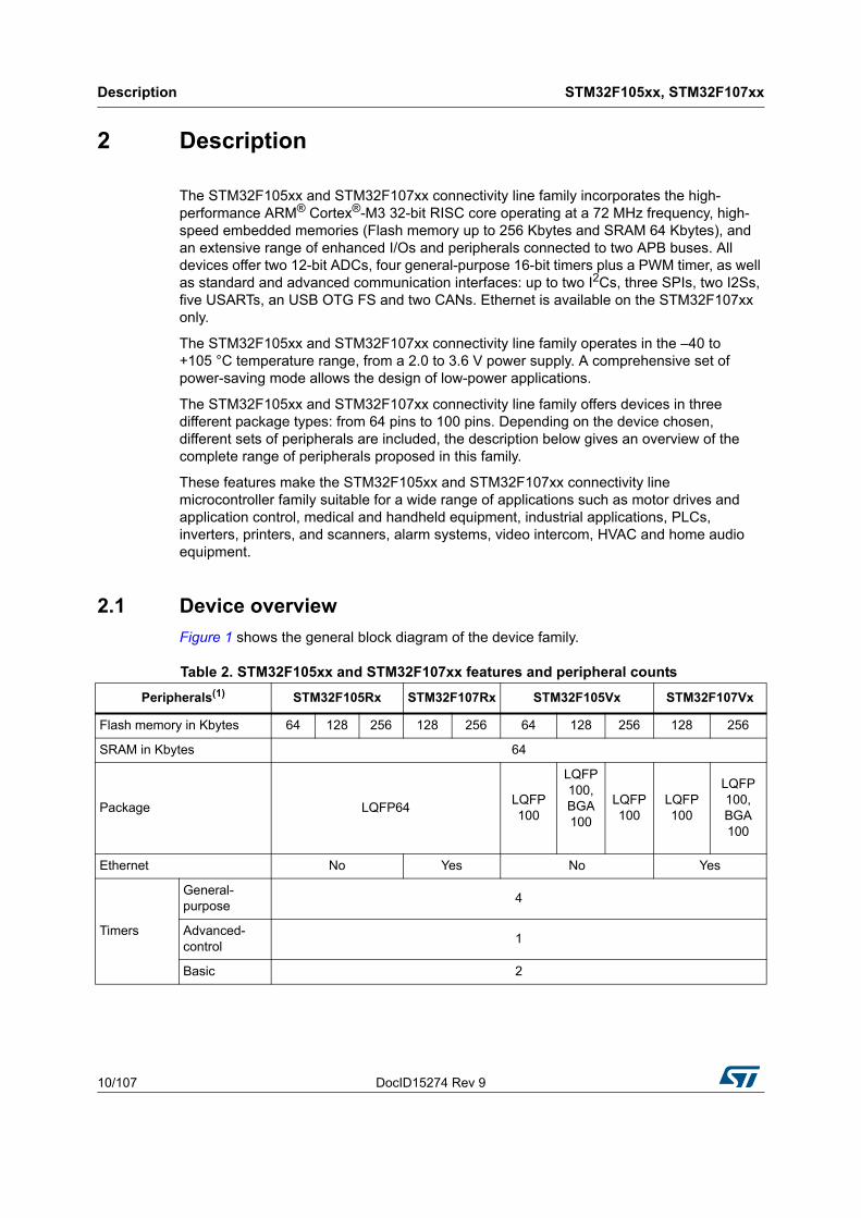
The STM32F105xx and STM32F107xx connectivity line family incorporates the high-performance ARM® Cortex®-M3 32-bit RISC core operating at a 72 MHz frequency, high-speed embedded memories (Flash memory up to 256 Kbytes and SRAM 64 Kbytes), and an extensive range of enhanced I/Os and peripherals connected to two APB buses. All devices offer two 12-bit ADCs, four general-purpose 16-bit timers plus a PWM timer, as well as standard and advanced communication interfaces: up to two I2Cs, three SPIs, two I2Ss, five USARTs, an USB OTG FS and two CANs. Ethernet is available on the STM32F107xx only.
The STM32F105xx and STM32F107xx connectivity line family operates in the –40 to +105 °C temperature range, from a 2.0 to 3.6 V power supply. A comprehensive set of power-saving mode allows the design of low-power applications.
The STM32F105xx and STM32F107xx connectivity line family offers devices in three different package types: from 64 pins to 100 pins. Depending on the device chosen, different sets of peripherals are included, the description below gives an overview of the complete range of peripherals proposed in this family.
These features make the STM32F105xx and STM32F107xx connectivity line microcontroller family suitable for a wide range of applications such as motor drives and application control, medical and handheld equipment, industrial applications, PLCs, inverters, printers, and scanners, alarm systems, video intercom, HVAC and home audio equipment.
2.1 Device overview
Figure 1 shows the general block diagram of the device family.
Table 2. STM32F105xx and STM32F107xx features and peripheral counts
Peripherals(1) STM32F105Rx STM32F107Rx STM32F105Vx STM32F107Vx
Flash memory in Kbytes 64 128 256 128 256 64 128 256 128 256
SRAM in Kbytes 64
Package LQFP64LQFP 100
LQFP100, BGA 100
LQFP100
LQFP 100
LQFP 100, BGA 100
Ethernet No Yes No Yes
Timers
General-purpose
4
Advanced-control
1
Basic 2

DocID15274 Rev 9 11/107
STM32F105xx, STM32F107xx Description
106
Communication interfaces
SPI(I2S)(2) 3(2) 3(2) 3(2) 3(2)
I2C 2 1 2 1
USART 5
USB OTG FS Yes
CAN 2
GPIOs 51 80
12-bit ADC
Number of channels
2
16
12-bit DAC
Number of channels
2
2
CPU frequency 72 MHz
Operating voltage 2.0 to 3.6 V
Operating temperaturesAmbient temperatures: –40 to +85 °C /–40 to +105 °C
Junction temperature: –40 to + 125 °C
1. Please refer to Table 5: Pin definitions for peripheral availability when the I/O pins are shared by the peripherals required by the application.
2. The SPI2 and SPI3 interfaces give the flexibility to work in either the SPI mode or the I2S audio mode.
Table 2. STM32F105xx and STM32F107xx features and peripheral counts (continued)
Peripherals(1) STM32F105Rx STM32F107Rx STM32F105Vx STM32F107Vx
Description STM32F105xx, STM32F107xx
12/107 DocID15274 Rev 9
2.2 Full compatibility throughout the family
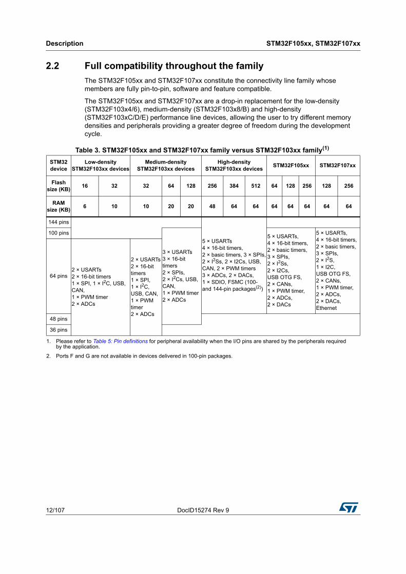
The STM32F105xx and STM32F107xx constitute the connectivity line family whose members are fully pin-to-pin, software and feature compatible.
The STM32F105xx and STM32F107xx are a drop-in replacement for the low-density (STM32F103x4/6), medium-density (STM32F103x8/B) and high-density (STM32F103xC/D/E) performance line devices, allowing the user to try different memory densities and peripherals providing a greater degree of freedom during the development cycle.
Table 3. STM32F105xx and STM32F107xx family versus STM32F103xx family(1)
STM32 device
Low-density STM32F103xx devices
Medium-density STM32F103xx devices
High-density STM32F103xx devices
STM32F105xx STM32F107xx
Flash size (KB)
16 32 32 64 128 256 384 512 64 128 256 128 256
RAM size (KB)
6 10 10 20 20 48 64 64 64 64 64 64 64
144 pins
5 × USARTs4 × 16-bit timers,2 × basic timers, 3 × SPIs,2 × I2Ss, 2 × I2Cs, USB, CAN, 2 × PWM timers3 × ADCs, 2 × DACs,1 × SDIO, FSMC (100- and 144-pin packages(2))
100 pins
3 × USARTs3 × 16-bit timers2 × SPIs,2 × I2Cs, USB, CAN,1 × PWM timer2 × ADCs
5 × USARTs,4 × 16-bit timers,2 × basic timers,3 × SPIs,2 × I2Ss,2 × I2Cs,USB OTG FS,2 × CANs,1 × PWM timer,2 × ADCs,2 × DACs
5 × USARTs,4 × 16-bit timers,2 × basic timers,3 × SPIs,2 × I2S,1 × I2C,USB OTG FS,2 × CANs,1 × PWM timer,2 × ADCs,2 × DACs,Ethernet
64 pins2 × USARTs2 × 16-bit timers1 × SPI, 1 × I2C, USB, CAN,1 × PWM timer2 × ADCs
2 × USARTs2 × 16-bit timers1 × SPI,1 × I2C, USB, CAN,1 × PWM timer2 × ADCs
48 pins
36 pins
1. Please refer to Table 5: Pin definitions for peripheral availability when the I/O pins are shared by the peripherals required by the application.
2. Ports F and G are not available in devices delivered in 100-pin packages.

DocID15274 Rev 9 13/107
STM32F105xx, STM32F107xx Description
106
2.3 Overview
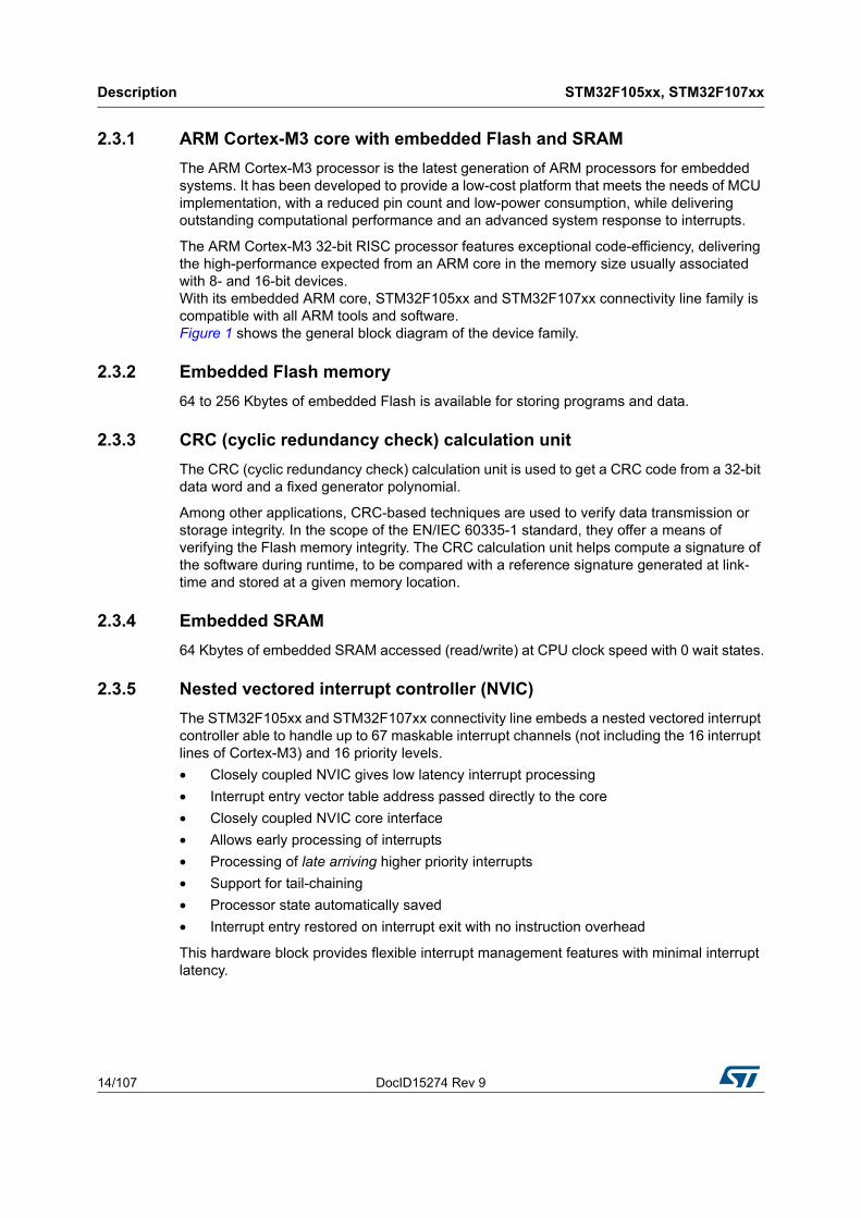
Figure 1. STM32F105xx and STM32F107xx connectivity line block diagram
1. TA = –40 °C to +85 °C (suffix 6, see Table 62) or –40 °C to +105 °C (suffix 7, see Table 62), junction temperature up to 105 °C or 125 °C, respectively.
2. AF = alternate function on I/O port pin.
PA[15:0]
EXT.IT
WWDG
12bi t ADC116 ADC12_INscommon toADC1 & ADC2
JTDIJTCK/SWCLKJTMS/SWDIO
NJTRST
JTDO
NRST
VDD = 2 to 3.6 V
80 AF
PB[15:0]
PC[15:0]
AHB toAPB2
CAN1_RX as AF
2x(8x16b it)
WKUP
GPIO port AP
GPIO port BP
Fmax: 72 MHz
VSS
SCL,SDA,SMBAI2C2
GP DMA1
TIM2
TIM3
XTAL osc3-25 MHz
XTAL 32kHz
OSC_INOSC_OUTC_O
OSC32_OUTOSC32_IN
AP
B1
: F
max
= 3
6 M
Hz
HCLK
as AF
Flash 256 KB
Voltage reg.3.3 V to 1.8 V
VDD18Power
Backup interface
as AF
TIM4
Bus
Mat
rix
64 bit
Inte
rfac
e
RTC
RC HS
Cortex-M3 CPUIbus
Dbus
obl
Flas
hl
SRAM 512B
USART1
USART2
SPI2 / I2S2(1)
bxCAN1
7 channels
Backupregister
4 Channels
TIM14 compl. Channels
SCL,SDA,SMBAI2C1as AF
RX,TX, CTS, RTS,USART3
Temp sensor
PD[15:0]
PE[15:0]
BKIN, ETR input as AF
4 Channels, ETR
4 Channels, ETR
4 Channels, ETR
FCLK
RC LS
Standby
IWDG
@VDD
@VBAT
POR / PDR
Supplysupervision
@VDDA
VDDAVSSA
@VDDA
VBAT=1.8 V to 3.6 V
CK as AF
RX,TX, CTS, RTS,CK as AF
RX,TX, CTS, RTS,CK as AF
AP
B2
: F
max
= 7
2 M
Hz
NVIC
SPI1MOSI,MISO,
SCK,NSS as AF
12bit ADC2
IF
IF
interface
PVD
Reset
Int
@VDD
AHB toAPB1
AWU
POR
TAMPER-RTC/ALARM/SECOND OUT
System
2x(8x16b it)SPI3 / I2S3
UART4
RX,TX as AFUART5
RX,TX as AF
TIM5 4 Channel s, ETR
Reset &clockcontrol
12bit DAC1IFIFIF
12bit DAC 2
@VDDA
USB OTG FS
SOFVBUS
IDDMDP
SRAM 64 KB
GP DMA2
5 channels
TIM6
TIM7
CAN1_TX as AF
SW/JTAG
TPIU ETMTrace/Trig
TRACECLKTRACED[0:3]
as AF
as AF
as AF
as AF
as AF
Ethernet MAC10/100
SRAM 1.25 KB
DPRAM 2 KB DPRAM 2 KB
MII_TXD[3:0]/RMII_TXD[1:0]MII_TX_CLK/RMII_TX_CLK
MII_TX_EN/RMII_TX_ENMII_RXD[3:0]/RMII_RXD[1:0]
MII_RX_ER/RMII_RX_ERMII_RX_CLK/RMII_REF_CLK
MII_RX_DV/RMII_CRS_DVMII_CRS
MII_COL/RMII_COLMDC
MDIOPPS_OUT
bxCAN2CAN2_RX as AF
CAN2_TX as AF
ai15411
DAC_OUT1 as AF
DAC_OUT2 as AF
@VDDA
PLL
GPIO port C
GPIO port D
GPIO port E
VREF+
VREF–
MOSI/SD, MISO, MCK,SCK/CK, NSS/WS as AF
MOSI/SD, MISO, MCK,SCK/CK, NSS/WS as AF
PCLK1PCLK2
PLL2
PLL3
PLL3
DMA Ethernet
AH
B
Description STM32F105xx, STM32F107xx
14/107 DocID15274 Rev 9
2.3.1 ARM Cortex-M3 core with embedded Flash and SRAM
The ARM Cortex-M3 processor is the latest generation of ARM processors for embedded systems. It has been developed to provide a low-cost platform that meets the needs of MCU implementation, with a reduced pin count and low-power consumption, while delivering outstanding computational performance and an advanced system response to interrupts.
The ARM Cortex-M3 32-bit RISC processor features exceptional code-efficiency, delivering the high-performance expected from an ARM core in the memory size usually associated with 8- and 16-bit devices.With its embedded ARM core, STM32F105xx and STM32F107xx connectivity line family is compatible with all ARM tools and software.Figure 1 shows the general block diagram of the device family.
2.3.2 Embedded Flash memory
64 to 256 Kbytes of embedded Flash is available for storing programs and data.
2.3.3 CRC (cyclic redundancy check) calculation unit
The CRC (cyclic redundancy check) calculation unit is used to get a CRC code from a 32-bit data word and a fixed generator polynomial.
Among other applications, CRC-based techniques are used to verify data transmission or storage integrity. In the scope of the EN/IEC 60335-1 standard, they offer a means of verifying the Flash memory integrity. The CRC calculation unit helps compute a signature of the software during runtime, to be compared with a reference signature generated at link-time and stored at a given memory location.
2.3.4 Embedded SRAM
64 Kbytes of embedded SRAM accessed (read/write) at CPU clock speed with 0 wait states.
2.3.5 Nested vectored interrupt controller (NVIC)
The STM32F105xx and STM32F107xx connectivity line embeds a nested vectored interrupt controller able to handle up to 67 maskable interrupt channels (not including the 16 interrupt lines of Cortex-M3) and 16 priority levels.
• Closely coupled NVIC gives low latency interrupt processing
• Interrupt entry vector table address passed directly to the core
• Closely coupled NVIC core interface
• Allows early processing of interrupts
• Processing of late arriving higher priority interrupts
• Support for tail-chaining
• Processor state automatically saved
• Interrupt entry restored on interrupt exit with no instruction overhead
This hardware block provides flexible interrupt management features with minimal interrupt latency.

DocID15274 Rev 9 15/107
STM32F105xx, STM32F107xx Description
106
2.3.6 External interrupt/event controller (EXTI)
The external interrupt/event controller consists of 20 edge detector lines used to generate interrupt/event requests. Each line can be independently configured to select the trigger event (rising edge, falling edge, both) and can be masked independently. A pending register maintains the status of the interrupt requests. The EXTI can detect an external line with a pulse width shorter than the Internal APB2 clock period. Up to 80 GPIOs can be connected to the 16 external interrupt lines.
2.3.7 Clocks and startup
System clock selection is performed on startup, however, the internal RC 8 MHz oscillator is selected as default CPU clock on reset. An external 3-25 MHz clock can be selected, in which case it is monitored for failure. If failure is detected, the system automatically switches back to the internal RC oscillator. A software interrupt is generated if enabled. Similarly, full interrupt management of the PLL clock entry is available when necessary (for example with failure of an indirectly used external oscillator).
A single 25 MHz crystal can clock the entire system including the ethernet and USB OTG FS peripherals. Several prescalers and PLLs allow the configuration of the AHB frequency, the high speed APB (APB2) and the low speed APB (APB1) domains. The maximum frequency of the AHB and the high speed APB domains is 72 MHz. The maximum allowed frequency of the low speed APB domain is 36 MHz. Refer to Figure 58: USB O44TG FS + Ethernet solution on page 99.
The advanced clock controller clocks the core and all peripherals using a single crystal or oscillator. In order to achieve audio class performance, an audio crystal can be used. In this case, the I2S master clock can generate all standard sampling frequencies from 8 kHz to 96 kHz with less than 0.5% accuracy error. Refer to Figure 59: USB OTG FS + I2S (Audio) solution on page 99.
To configure the PLLs, please refer to Table 63 on page 100, which provides PLL configurations according to the application type.
2.3.8 Boot modes
At startup, boot pins are used to select one of three boot options:
• Boot from User Flash
• Boot from System Memory
• Boot from embedded SRAM
The boot loader is located in System Memory. It is used to reprogram the Flash memory by using USART1, USART2 (remapped), CAN2 (remapped) or USB OTG FS in device mode (DFU: device firmware upgrade). For remapped signals refer to Table 5: Pin definitions.
The USART peripheral operates with the internal 8 MHz oscillator (HSI), however the CAN and USB OTG FS can only function if an external 8 MHz, 14.7456 MHz or 25 MHz clock (HSE) is present.
For full details about the boot loader, please refer to AN2606.

Description STM32F105xx, STM32F107xx
16/107 DocID15274 Rev 9
2.3.9 Power supply schemes
• VDD = 2.0 to 3.6 V: external power supply for I/Os and the internal regulator. Provided externally through VDD pins.
• VSSA, VDDA = 2.0 to 3.6 V: external analog power supplies for ADC, Reset blocks, RCs and PLL (minimum voltage to be applied to VDDA is 2.4 V when the ADC is used). VDDA and VSSA must be connected to VDD and VSS, respectively.
• VBAT = 1.8 to 3.6 V: power supply for RTC, external clock 32 kHz oscillator and backup registers (through power switch) when VDD is not present.
2.3.10 Power supply supervisor
The device has an integrated power-on reset (POR)/power-down reset (PDR) circuitry. It is always active, and ensures proper operation starting from/down to 2 V. The device remains in reset mode when VDD is below a specified threshold, VPOR/PDR, without the need for an external reset circuit.
The device features an embedded programmable voltage detector (PVD) that monitors the VDD/VDDA power supply and compares it to the VPVD threshold. An interrupt can be generated when VDD/VDDA drops below the VPVD threshold and/or when VDD/VDDA is higher than the VPVD threshold. The interrupt service routine can then generate a warning message and/or put the MCU into a safe state. The PVD is enabled by software.
2.3.11 Voltage regulator
The regulator has three operation modes: main (MR), low power (LPR) and power down.
• MR is used in the nominal regulation mode (Run)
• LPR is used in the Stop modes.
• Power down is used in Standby mode: the regulator output is in high impedance: the kernel circuitry is powered down, inducing zero consumption (but the contents of the registers and SRAM are lost)
This regulator is always enabled after reset. It is disabled in Standby mode.
2.3.12 Low-power modes
The STM32F105xx and STM32F107xx connectivity line supports three low-power modes to achieve the best compromise between low power consumption, short startup time and available wakeup sources:
• Sleep mode
In Sleep mode, only the CPU is stopped. All peripherals continue to operate and can wake up the CPU when an interrupt/event occurs.
• Stop mode
Stop mode achieves the lowest power consumption while retaining the content of SRAM and registers. All clocks in the 1.8 V domain are stopped, the PLL, the HSI RC and the HSE crystal oscillators are disabled. The voltage regulator can also be put either in normal or in low-power mode. The device can be woken up from Stop mode by any of the EXTI line. The EXTI line source can be one of the 16 external lines, the PVD output, the RTC alarm or the USB OTG FS wakeup.

DocID15274 Rev 9 17/107
STM32F105xx, STM32F107xx Description
106
• Standby mode
The Standby mode is used to achieve the lowest power consumption. The internal voltage regulator is switched off so that the entire 1.8 V domain is powered off. The PLL, the HSI RC and the HSE crystal oscillators are also switched off. After entering Standby mode, SRAM and register contents are lost except for registers in the Backup domain and Standby circuitry.
The device exits Standby mode when an external reset (NRST pin), an IWDG reset, a rising edge on the WKUP pin, or an RTC alarm occurs.
Note: The RTC, the IWDG, and the corresponding clock sources are not stopped by entering Stop or Standby mode.
2.3.13 DMA
The flexible 12-channel general-purpose DMAs (7 channels for DMA1 and 5 channels for DMA2) are able to manage memory-to-memory, peripheral-to-memory and memory-to-peripheral transfers. The two DMA controllers support circular buffer management, removing the need for user code intervention when the controller reaches the end of the buffer.Each channel is connected to dedicated hardware DMA requests, with support for software trigger on each channel. Configuration is made by software and transfer sizes between source and destination are independent.
The DMA can be used with the main peripherals: SPI, I2C, USART, general-purpose, basic and advanced control timers TIMx, DAC, I2S and ADC.
In the STM32F107xx, there is a DMA controller dedicated for use with the Ethernet (see Section 2.3.20: Ethernet MAC interface with dedicated DMA and IEEE 1588 support for more information).
2.3.14 RTC (real-time clock) and backup registers
The RTC and the backup registers are supplied through a switch that takes power either on VDD supply when present or through the VBAT pin. The backup registers are forty-two 16-bit registers used to store 84 bytes of user application data when VDD power is not present. They are not reset by a system or power reset, and they are not reset when the device wakes up from the Standby mode.
The real-time clock provides a set of continuously running counters which can be used with suitable software to provide a clock calendar function, and provides an alarm interrupt and a periodic interrupt. It is clocked by a 32.768 kHz external crystal, resonator or oscillator, the internal low power RC oscillator or the high-speed external clock divided by 128. The internal low-speed RC has a typical frequency of 40 kHz. The RTC can be calibrated using an external 512 Hz output to compensate for any natural quartz deviation. The RTC features a 32-bit programmable counter for long term measurement using the Compare register to generate an alarm. A 20-bit prescaler is used for the time base clock and is by default configured to generate a time base of 1 second from a clock at 32.768 kHz.
For more information, please refer to AN2604: “STM32F101xx and STM32F103xx RTC calibration”, available from www.st.com.

Description STM32F105xx, STM32F107xx
18/107 DocID15274 Rev 9
2.3.15 Timers and watchdogs
The STM32F105xx and STM32F107xx devices include an advanced-control timer, four general-purpose timers, two basic timers, two watchdog timers and a SysTick timer.
Table 4 compares the features of the general-purpose and basic timers.
Advanced-control timer (TIM1)
The advanced control timer (TIM1) can be seen as a three-phase PWM multiplexed on 6 channels. It has complementary PWM outputs with programmable inserted dead-times. It can also be seen as a complete general-purpose timer. The 4 independent channels can be used for:
• Input capture
• Output compare
• PWM generation (edge or center-aligned modes)
• One-pulse mode output
If configured as a standard 16-bit timer, it has the same features as the TIMx timer. If configured as the 16-bit PWM generator, it has full modulation capability (0-100%).
The counter can be frozen in debug mode.
Many features are shared with those of the standard TIM timers which have the same architecture. The advanced control timer can therefore work together with the TIM timers via the Timer Link feature for synchronization or event chaining.
General-purpose timers (TIMx)
There are up to 4 synchronizable standard timers (TIM2, TIM3, TIM4 and TIM5) embedded in the STM32F105xx and STM32F107xx connectivity line devices. These timers are based on a 16-bit auto-reload up/down counter, a 16-bit prescaler and feature 4 independent channels each for input capture/output compare, PWM or one pulse mode output. This gives up to 16 input captures / output compares / PWMs on the largest packages. They can work together with the Advanced Control timer via the Timer Link feature for synchronization or event chaining.
The counter can be frozen in debug mode.
Table 4. Timer feature comparison
TimerCounter
resolutionCounter
typePrescaler
factorDMA request generation
Capture/compare channels
Complementaryoutputs
TIM1 16-bitUp,
down, up/down
Any integer between 1 and 65536
Yes 4 Yes
TIMx (TIM2, TIM3, TIM4, TIM5)
16-bitUp,
down, up/down
Any integer between 1 and 65536
Yes 4 No
TIM6, TIM7
16-bit UpAny integer between 1 and 65536
Yes 0 No

DocID15274 Rev 9 19/107
STM32F105xx, STM32F107xx Description
106
Any of the standard timers can be used to generate PWM outputs. Each of the timers has independent DMA request generations.
Basic timers TIM6 and TIM7
These timers are mainly used for DAC trigger generation. They can also be used as a generic 16-bit time base.
Independent watchdog
The independent watchdog is based on a 12-bit downcounter and 8-bit prescaler. It is clocked from an independent 40 kHz internal RC and as it operates independently from the main clock, it can operate in Stop and Standby modes. It can be used either as a watchdog to reset the device when a problem occurs, or as a free running timer for application timeout management. It is hardware or software configurable through the option bytes. The counter can be frozen in debug mode.
Window watchdog
The window watchdog is based on a 7-bit downcounter that can be set as free running. It can be used as a watchdog to reset the device when a problem occurs. It is clocked from the main clock. It has an early warning interrupt capability and the counter can be frozen in debug mode.
SysTick timer
This timer is dedicated to real-time operating systems, but could also be used as a standard down counter. It features:
• A 24-bit down counter
• Autoreload capability
• Maskable system interrupt generation when the counter reaches 0.
• Programmable clock source
2.3.16 I²C bus
Up to two I²C bus interfaces can operate in multimaster and slave modes. They can support standard and fast modes.
They support 7/10-bit addressing mode and 7-bit dual addressing mode (as slave). A hardware CRC generation/verification is embedded.
They can be served by DMA and they support SMBus 2.0/PMBus.
2.3.17 Universal synchronous/asynchronous receiver transmitters (USARTs)
The STM32F105xx and STM32F107xx connectivity line embeds three universal synchronous/asynchronous receiver transmitters (USART1, USART2 and USART3) and two universal asynchronous receiver transmitters (UART4 and UART5).
These five interfaces provide asynchronous communication, IrDA SIR ENDEC support, multiprocessor communication mode, single-wire half-duplex communication mode and have LIN Master/Slave capability.
The USART1 interface is able to communicate at speeds of up to 4.5 Mbit/s. The other available interfaces communicate at up to 2.25 Mbit/s.
Description STM32F105xx, STM32F107xx
20/107 DocID15274 Rev 9
USART1, USART2 and USART3 also provide hardware management of the CTS and RTS signals, Smart Card mode (ISO 7816 compliant) and SPI-like communication capability. All interfaces can be served by the DMA controller except for UART5.
2.3.18 Serial peripheral interface (SPI)
Up to three SPIs are able to communicate up to 18 Mbits/s in slave and master modes in full-duplex and simplex communication modes. The 3-bit prescaler gives 8 master mode frequencies and the frame is configurable to 8 bits or 16 bits. The hardware CRC generation/verification supports basic SD Card/MMC/SDHC(a) modes.
All SPIs can be served by the DMA controller.
2.3.19 Inter-integrated sound (I2S)
Two standard I2S interfaces (multiplexed with SPI2 and SPI3) are available, that can be operated in master or slave mode. These interfaces can be configured to operate with 16/32 bit resolution, as input or output channels. Audio sampling frequencies from 8 kHz up to 96 kHz are supported. When either or both of the I2S interfaces is/are configured in master mode, the master clock can be output to the external DAC/CODEC at 256 times the sampling frequency with less than 0.5% accuracy error owing to the advanced clock controller (see Section 2.3.7: Clocks and startup).
Please refer to the “Audio frequency precision” tables provided in the “Serial peripheral interface (SPI)” section of the STM32F10xxx reference manual.
2.3.20 Ethernet MAC interface with dedicated DMA and IEEE 1588 support
Peripheral not available on STM32F105xx devices.
The STM32F107xx devices provide an IEEE-802.3-2002-compliant media access controller (MAC) for ethernet LAN communications through an industry-standard media-independent interface (MII) or a reduced media-independent interface (RMII). The STM32F107xx requires an external physical interface device (PHY) to connect to the physical LAN bus (twisted-pair, fiber, etc.). the PHY is connected to the STM32F107xx MII port using as many as 17 signals (MII) or 9 signals (RMII) and can be clocked using the 25 MHz (MII) or 50 MHz (RMII) output from the STM32F107xx.
The STM32F107xx includes the following features:
• Supports 10 and 100 Mbit/s rates
• Dedicated DMA controller allowing high-speed transfers between the dedicated SRAM and the descriptors (see the STM32F105xx/STM32F107xx reference manual for details)
• Tagged MAC frame support (VLAN support)
• Half-duplex (CSMA/CD) and full-duplex operation
• MAC control sublayer (control frames) support
a. SDHC = Secure digital high capacity.

DocID15274 Rev 9 21/107
STM32F105xx, STM32F107xx Description
106
• 32-bit CRC generation and removal
• Several address filtering modes for physical and multicast address (multicast and group addresses)
• 32-bit status code for each transmitted or received frame
• Internal FIFOs to buffer transmit and receive frames. The transmit FIFO and the receive FIFO are both 2 Kbytes, that is 4 Kbytes in total
• Supports hardware PTP (precision time protocol) in accordance with IEEE 1588 with the timestamp comparator connected to the TIM2 trigger input
• Triggers interrupt when system time becomes greater than target time
2.3.21 Controller area network (CAN)
The two CANs are compliant with the 2.0A and B (active) specifications with a bitrate up to 1 Mbit/s. They can receive and transmit standard frames with 11-bit identifiers as well as extended frames with 29-bit identifiers. Each CAN has three transmit mailboxes, two receive FIFOS with 3 stages and 28 shared scalable filter banks (all of them can be used even if one CAN is used). The 256 bytes of SRAM which are allocated for each CAN (512 bytes in total) are not shared with any other peripheral.
2.3.22 Universal serial bus on-the-go full-speed (USB OTG FS)
The STM32F105xx and STM32F107xx connectivity line devices embed a USB OTG full-speed (12 Mb/s) device/host/OTG peripheral with integrated transceivers. The USB OTG FS peripheral is compliant with the USB 2.0 specification and with the OTG 1.0 specification. It has software-configurable endpoint setting and supports suspend/resume. The USB OTG full-speed controller requires a dedicated 48 MHz clock that is generated by a PLL connected to the HSE oscillator. The major features are:
• 1.25 KB of SRAM used exclusively by the endpoints (not shared with any other peripheral)
• 4 bidirectional endpoints
• HNP/SNP/IP inside (no need for any external resistor)
• for OTG/Host modes, a power switch is needed in case bus-powered devices are connected
• the SOF output can be used to synchronize the external audio DAC clock in isochronous mode
• in accordance with the USB 2.0 Specification, the supported transfer speeds are:
– in Host mode: full speed and low speed
– in Device mode: full speed
2.3.23 GPIOs (general-purpose inputs/outputs)
Each of the GPIO pins can be configured by software as output (push-pull or open-drain), as input (with or without pull-up or pull-down) or as peripheral alternate function. Most of the GPIO pins are shared with digital or analog alternate functions. All GPIOs are high current-capable.
The I/Os alternate function configuration can be locked if needed following a specific sequence in order to avoid spurious writing to the I/Os registers.
I/Os on APB2 with up to 18 MHz toggling speed

Description STM32F105xx, STM32F107xx
22/107 DocID15274 Rev 9
2.3.24 Remap capability
This feature allows the use of a maximum number of peripherals in a given application. Indeed, alternate functions are available not only on the default pins but also on other specific pins onto which they are remappable. This has the advantage of making board design and port usage much more flexible.
For details refer to Table 5: Pin definitions; it shows the list of remappable alternate functions and the pins onto which they can be remapped. See the STM32F10xxx reference manual for software considerations.
2.3.25 ADCs (analog-to-digital converters)
Two 12-bit analog-to-digital converters are embedded into STM32F105xx and STM32F107xx connectivity line devices and each ADC shares up to 16 external channels, performing conversions in single-shot or scan modes. In scan mode, automatic conversion is performed on a selected group of analog inputs.
Additional logic functions embedded in the ADC interface allow:
• Simultaneous sample and hold
• Interleaved sample and hold
• Single shunt
The ADC can be served by the DMA controller.
An analog watchdog feature allows very precise monitoring of the converted voltage of one, some or all selected channels. An interrupt is generated when the converted voltage is outside the programmed thresholds.
The events generated by the standard timers (TIMx) and the advanced-control timer (TIM1) can be internally connected to the ADC start trigger and injection trigger, respectively, to allow the application to synchronize A/D conversion and timers.
2.3.26 DAC (digital-to-analog converter)
The two 12-bit buffered DAC channels can be used to convert two digital signals into two analog voltage signal outputs. The chosen design structure is composed of integrated resistor strings and an amplifier in inverting configuration.
This dual digital Interface supports the following features:
• two DAC converters: one for each output channel
• 8-bit or 12-bit monotonic output
• left or right data alignment in 12-bit mode
• synchronized update capability
• noise-wave generation
• triangular-wave generation
• dual DAC channel independent or simultaneous conversions
• DMA capability for each channel
• external triggers for conversion
• input voltage reference VREF+

DocID15274 Rev 9 23/107
STM32F105xx, STM32F107xx Description
106
Eight DAC trigger inputs are used in the STM32F105xx and STM32F107xx connectivity line family. The DAC channels are triggered through the timer update outputs that are also connected to different DMA channels.
2.3.27 Temperature sensor
The temperature sensor has to generate a voltage that varies linearly with temperature. The conversion range is between 2 V < VDDA < 3.6 V. The temperature sensor is internally connected to the ADC1_IN16 input channel which is used to convert the sensor output voltage into a digital value.
2.3.28 Serial wire JTAG debug port (SWJ-DP)
The ARM SWJ-DP Interface is embedded, and is a combined JTAG and serial wire debug port that enables either a serial wire debug or a JTAG probe to be connected to the target. The JTAG TMS and TCK pins are shared respectively with SWDIO and SWCLK and a specific sequence on the TMS pin is used to switch between JTAG-DP and SW-DP.
2.3.29 Embedded Trace Macrocell™
The ARM® Embedded Trace Macrocell provides a greater visibility of the instruction and data flow inside the CPU core by streaming compressed data at a very high rate from the STM32F10xxx through a small number of ETM pins to an external hardware trace port analyzer (TPA) device. The TPA is connected to a host computer using USB, Ethernet, or any other high-speed channel. Real-time instruction and data flow activity can be recorded and then formatted for display on the host computer running debugger software. TPA hardware is commercially available from common development tool vendors. It operates with third party debugger software tools.

Pinouts and pin description STM32F105xx, STM32F107xx
24/107 DocID15274 Rev 9
3 Pinouts and pin description
Figure 2. STM32F105xx and STM32F107xx connectivity line BGA100 ballout top view
AI14601c
PE10
PC14-OSC32_IN
PC5PA5
PC3
PB4
PE15
PB2PC4PA4
H
PE14
PE11PE7
D PD4
PD3
PB8PE3
C
PD0
PC12
PE5
PB5
PC0
PE2
B PC11PD2PC15-
OSC32_OUT
PB7
PB6
A
87654321
VSS_5OSC_IN
OSC_OUT VDD_5
G
F
E
PC1
VREF–
PC13-TAMPER-RTC
PB9 PA15PB3
PE4 PE1
PE0
VSS_1 PD1PE6NRST PC2 VSS_3VSS_4
NCVDD_3VDD_4
PB15
VBAT PD5
PD6
BOOT0 PD7
�VSS_2
VSSA
PA1
VDD_2 VDD_1
PB14
PA0-WKUP
109
K
J
PD10
PD11
PA8
PA9
PA10
PA11
PA12PC10
PA13PA14
PC9 PC7
PC6
PD15
PC8
PD14
PE12
PB1PA7 PB11
PE8PB0PA6 PB10
PE13PE9VDDA
PB13VREF+
PA3 PB12
PA2
PD8
PD9 PD13
PD12

DocID15274 Rev 9 25/107
STM32F105xx, STM32F107xx Pinouts and pin description
106
Figure 3. STM32F105xx and STM32F107xx connectivity line LQFP100 pinout

Pinouts and pin description STM32F105xx, STM32F107xx
26/107 DocID15274 Rev 9
Figure 4. STM32F105xx and STM32F107xx connectivity line LQFP64 pinout

DocID15274 Rev 9 27/107
STM32F105xx, STM32F107xx Pinouts and pin description
106
Table 5. Pin definitions
Pins
Pin name
Typ
e(1)
I / O
Le
vel(2
)
Main function(3) (after reset)
Alternate functions(4)
BG
A1
00
LQ
FP
64
LQ
FP
100
Default Remap
A3 - 1 PE2 I/O FT PE2 TRACECK -
B3 - 2 PE3 I/O FT PE3 TRACED0 -
C3 - 3 PE4 I/O FT PE4 TRACED1 -
D3 - 4 PE5 I/O FT PE5 TRACED2 -
E3 - 5 PE6 I/O FT PE6 TRACED3 -
B2 1 6 VBAT S - VBAT - -
A2 2 7PC13-TAMPER-
RTC(5) I/O - PC13(6) TAMPER-RTC -
A1 3 8PC14-
OSC32_IN(5) I/O - PC14(6) OSC32_IN -
B1 4 9PC15-
OSC32_OUT(5) I/O - PC15(6) OSC32_OUT -
C2 - 10 VSS_5 S - VSS_5 - -
D2 - 11 VDD_5 S - VDD_5 - -
C1 5 12 OSC_IN I - OSC_IN - -
D1 6 13 OSC_OUT O - OSC_OUT - -
E1 7 14 NRST I/O - NRST - -
F1 8 15 PC0 I/O - PC0 ADC12_IN10 -
F2 9 16 PC1 I/O - PC1ADC12_IN11/ ETH_MII_MDC/
ETH_RMII_MDC -
E2 10 17 PC2 I/O - PC2 ADC12_IN12/ ETH_MII_TXD2 -
F3 11 18 PC3 I/O - PC3ADC12_IN13/
ETH_MII_TX_CLK -
G1 12 19 VSSA S - VSSA - -
H1 - 20 VREF- S - VREF- - -
J1 - 21 VREF+ S - VREF+ - -
K1 13 22 VDDA S - VDDA - -
G2 14 23 PA0-WKUP I/O - PA0
WKUP/USART2_CTS(7)
ADC12_IN0/TIM2_CH1_ETRTIM5_CH1/
ETH_MII_CRS_WKUP
-

Pinouts and pin description STM32F105xx, STM32F107xx
28/107 DocID15274 Rev 9
H2 15 24 PA1 I/O - PA1
USART2_RTS(7)/ ADC12_IN1/ TIM5_CH2 /TIM2_CH2(7)/
ETH_MII_RX_CLK/ETH_RMII_REF_CLK
-
J2 16 25 PA2 I/O - PA2
USART2_TX(7)/TIM5_CH3/ADC12_IN2/
TIM2_CH3 (7)/ ETH_MII_MDIO/ETH_RMII_MDIO
-
K2 17 26 PA3 I/O - PA3USART2_RX(7)/
TIM5_CH4/ADC12_IN3 /TIM2_CH4(7)/ ETH_MII_COL
-
E4 18 27 VSS_4 S - VSS_4 - -
F4 19 28 VDD_4 S - VDD_4 - -
G3 20 29 PA4 I/O - PA4SPI1_NSS(7)/DAC_OUT1 /
USART2_CK(7) / ADC12_IN4SPI3_NSS/I2S3_WS
H3 21 30 PA5 I/O - PA5SPI1_SCK(7) /
DAC_OUT2 / ADC12_IN5 -
J3 22 31 PA6 I/O - PA6SPI1_MISO(7)/ADC12_IN6 /
TIM3_CH1(7) TIM1_BKIN
K3 23 32 PA7 I/O - PA7
SPI1_MOSI(7)/ADC12_IN7 /TIM3_CH2(7)/
ETH_MII_RX_DV(8)/ETH_RMII_CRS_DV
TIM1_CH1N
G4 24 33 PC4 I/O - PC4ADC12_IN14/
ETH_MII_RXD0(8)/ETH_RMII_RXD0
-
H4 25 34 PC5 I/O - PC5ADC12_IN15/
ETH_MII_RXD1(8)/ETH_RMII_RXD1
-
J4 26 35 PB0 I/O - PB0ADC12_IN8/TIM3_CH3/
ETH_MII_RXD2(8) TIM1_CH2N
K4 27 36 PB1 I/O - PB1ADC12_IN9/TIM3_CH4(7)/
ETH_MII_RXD3(8) TIM1_CH3N
G5 28 37 PB2 I/O FT PB2/BOOT1 - -
H5 - 38 PE7 I/O FT PE7 - TIM1_ETR
J5 - 39 PE8 I/O FT PE8 - TIM1_CH1N
Table 5. Pin definitions (continued)
Pins
Pin name
Typ
e(1
)
I / O
Lev
el(2
)
Main function(3) (after reset)
Alternate functions(4)
BG
A10
0
LQ
FP
64
LQ
FP
100
Default Remap
DocID15274 Rev 9 29/107
STM32F105xx, STM32F107xx Pinouts and pin description
106
K5 - 40 PE9 I/O FT PE9 - TIM1_CH1
- - - VSS_7 S - - - -
- - - VDD_7 S - - - -
G6 - 41 PE10 I/O FT PE10 - TIM1_CH2N
H6 - 42 PE11 I/O FT PE11 - TIM1_CH2
J6 - 43 PE12 I/O FT PE12 - TIM1_CH3N
K6 - 44 PE13 I/O FT PE13 - TIM1_CH3
G7 - 45 PE14 I/O FT PE14 - TIM1_CH4
H7 - 46 PE15 I/O FT PE15 - TIM1_BKIN
J7 29 47 PB10 I/O FT PB10I2C2_SCL(8)/USART3_TX(7)/
ETH_MII_RX_ERTIM2_CH3
K7 30 48 PB11 I/O FT PB11I2C2_SDA(8)/USART3_RX(7)/
ETH_MII_TX_EN/ETH_RMII_TX_EN
TIM2_CH4
E7 31 49 VSS_1 S - VSS_1 - -
F7 32 50 VDD_1 S - VDD_1 - -
K8 33 51 PB12 I/O FT PB12
SPI2_NSS(8)/I2S2_WS(8)/I2C2_SMBA(8) /
USART3_CK(7)/ TIM1_BKIN(7) / CAN2_RX/ ETH_MII_TXD0/
ETH_RMII_TXD0
-
J8 34 52 PB13 I/O FT PB13
SPI2_SCK(8) / I2S2_CK(8) /USART3_CTS(7)/
TIM1_CH1N/CAN2_TX/ETH_MII_TXD1/ETH_RMII_TXD1
-
H8 35 53 PB14 I/O FT PB14SPI2_MISO(8) / TIM1_CH2N /
USART3_RTS(7) -
G8 36 54 PB15 I/O FT PB15SPI2_MOSI(8) / I2S2_SD(8) /
TIM1_CH3N(7) -
K9 - 55 PD8 I/O FT PD8 - USART3_TX/
ETH_MII_RX_DV/ETH_RMII_CRS_DV
Table 5. Pin definitions (continued)
Pins
Pin name
Typ
e(1
)
I / O
Lev
el(2
)
Main function(3) (after reset)
Alternate functions(4)
BG
A10
0
LQ
FP
64
LQ
FP
100
Default Remap

Pinouts and pin description STM32F105xx, STM32F107xx
30/107 DocID15274 Rev 9
J9 - 56 PD9 I/O FT PD9 - USART3_RX/
ETH_MII_RXD0/ETH_RMII_RXD0
H9 - 57 PD10 I/O FT PD10 - USART3_CK/
ETH_MII_RXD1/ETH_RMII_RXD1
G9 - 58 PD11 I/O FT PD11 - USART3_CTS/ETH_MII_RXD2
K10 - 59 PD12 I/O FT PD12 - TIM4_CH1 /
USART3_RTS/ETH_MII_RXD3
J10 - 60 PD13 I/O FT PD13 - TIM4_CH2
H10 - 61 PD14 I/O FT PD14 - TIM4_CH3
G10 - 62 PD15 I/O FT PD15 - TIM4_CH4
F10 37 63 PC6 I/O FT PC6 I2S2_MCK/ TIM3_CH1
E10 38 64 PC7 I/O FT PC7 I2S3_MCK TIM3_CH2
F9 39 65 PC8 I/O FT PC8 - TIM3_CH3
E9 40 66 PC9 I/O FT PC9 - TIM3_CH4
D9 41 67 PA8 I/O FT PA8USART1_CK/OTG_FS_SOF /
TIM1_CH1(8)/MCO -
C9 42 68 PA9 I/O FT PA9USART1_TX(7)/ TIM1_CH2(7)/
OTG_FS_VBUS -
D10 43 69 PA10 I/O FT PA10USART1_RX(7)/
TIM1_CH3(7)/OTG_FS_ID -
C10 44 70 PA11 I/O FT PA11USART1_CTS / CAN1_RX /TIM1_CH4(7)/OTG_FS_DM
-
B10 45 71 PA12 I/O FT PA12USART1_RTS / OTG_FS_DP /
CAN1_TX(7) / TIM1_ETR(7) -
A10 46 72 PA13 I/O FT JTMS-SWDIO - PA13
F8 - 73 Not connected -
E6 47 74 VSS_2 S - VSS_2 - -
F6 48 75 VDD_2 S - VDD_2 - -
A9 49 76 PA14 I/O FT JTCK-SWCLK - PA14
Table 5. Pin definitions (continued)
Pins
Pin name
Typ
e(1
)
I / O
Lev
el(2
)
Main function(3) (after reset)
Alternate functions(4)
BG
A10
0
LQ
FP
64
LQ
FP
100
Default Remap
DocID15274 Rev 9 31/107
STM32F105xx, STM32F107xx Pinouts and pin description
106
A8 50 77 PA15 I/O FT JTDI SPI3_NSS / I2S3_WSTIM2_CH1_ETR / PA15
SPI1_NSS
B9 51 78 PC10 I/O FT PC10 UART4_TXUSART3_TX/
SPI3_SCK/I2S3_CK
B8 52 79 PC11 I/O FT PC11 UART4_RXUSART3_RX/ SPI3_MISO
C8 53 80 PC12 I/O FT PC12 UART5_TXUSART3_CK/
SPI3_MOSI/I2S3_SD
- - 81 PD0 I/O FT PD0 - OSC_IN(9)/CAN1_RX
- - 82 PD1 I/O FT PD1 - OSC_OUT(9)/CAN1_TX
B7 54 83 PD2 I/O FT PD2 TIM3_ETR / UART5_RX
C7 - 84 PD3 I/O FT PD3 - USART2_CTS
D7 - 85 PD4 I/O FT PD4 - USART2_RTS
B6 - 86 PD5 I/O FT PD5 - USART2_TX
C6 - 87 PD6 I/O FT PD6 - USART2_RX
D6 - 88 PD7 I/O FT PD7 - USART2_CK
A7 55 89 PB3 I/O FT JTDO SPI3_SCK / I2S3_CKPB3 / TRACESWO/
TIM2_CH2 / SPI1_SCK
A6 56 90 PB4 I/O FT NJTRST SPI3_MISOPB4 / TIM3_CH1/
SPI1_MISO
C5 57 91 PB5 I/O - PB5I2C1_SMBA / SPI3_MOSI /
ETH_MII_PPS_OUT / I2S3_SDETH_RMII_PPS_OUT
TIM3_CH2/SPI1_MOSI/CAN2_RX
B5 58 92 PB6 I/O FT PB6 I2C1_SCL(7)/TIM4_CH1(7) USART1_TX/CAN2_TX
A5 59 93 PB7 I/O FT PB7 I2C1_SDA(7)/TIM4_CH2(7) USART1_RX
D5 60 94 BOOT0 I - BOOT0 - -
B4 61 95 PB8 I/O FT PB8 TIM4_CH3(7)/ ETH_MII_TXD3 I2C1_SCL/CAN1_RX
A4 62 96 PB9 I/O FT PB9 TIM4_CH4(7) I2C1_SDA / CAN1_TX
D4 - 97 PE0 I/O FT PE0 TIM4_ETR -
C4 - 98 PE1 I/O FT PE1 - -
E5 63 99 VSS_3 S - VSS_3 - -
F5 64 100 VDD_3 S - VDD_3 - -
Table 5. Pin definitions (continued)
Pins
Pin name
Typ
e(1
)
I / O
Lev
el(2
)
Main function(3) (after reset)
Alternate functions(4)
BG
A10
0
LQ
FP
64
LQ
FP
100
Default Remap
Pinouts and pin description STM32F105xx, STM32F107xx
32/107 DocID15274 Rev 9
1. I = input, O = output, S = supply, HiZ = high impedance.
2. FT = 5 V tolerant. All I/Os are VDD capable.
3. Function availability depends on the chosen device.
4. If several peripherals share the same I/O pin, to avoid conflict between these alternate functions only one peripheral should be enabled at a time through the peripheral clock enable bit (in the corresponding RCC peripheral clock enable register).
5. PC13, PC14 and PC15 are supplied through the power switch, and so their use in output mode is limited: they can be used only in output 2 MHz mode with a maximum load of 30 pF and only one pin can be put in output mode at a time.
6. Main function after the first backup domain power-up. Later on, it depends on the contents of the Backup registers even after reset (because these registers are not reset by the main reset). For details on how to manage these IOs, refer to the Battery backup domain and BKP register description sections in the STM32F10xxx reference manual, available from the STMicroelectronics website: www.st.com.
7. This alternate function can be remapped by software to some other port pins (if available on the used package). For more details, refer to the Alternate function I/O and debug configuration section in the STM32F10xxx reference manual, available from the STMicroelectronics website: www.st.com.
8. SPI2/I2S2 and I2C2 are not available when the Ethernet is being used.
9. For the LQFP64 package, the pins number 5 and 6 are configured as OSC_IN/OSC_OUT after reset, however the functionality of PD0 and PD1 can be remapped by software on these pins. For the LQFP100 and BGA100 packages, PD0 and PD1 are available by default, so there is no need for remapping. For more details, refer to Alternate function I/O and debug configuration section in the STM32F10xxx reference manual.
DocID15274 Rev 9 33/107
STM32F105xx, STM32F107xx Memory mapping
106
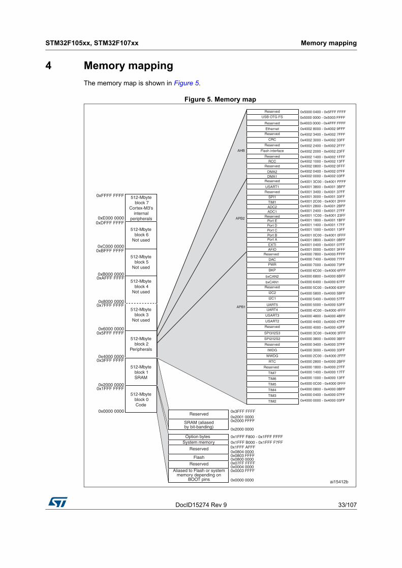
4 Memory mapping
The memory map is shown in Figure 5.
Figure 5. Memory map
512-Mbyte block 7
Cortex-M3'sinternal
peripherals
512-Mbyte block 6
Not used
512-Mbyte block 5
Not used
512-Mbyte block 4
Not used
512-Mbyte block 3
Not used
512-Mbyte block 2
Peripherals
512-Mbyte block 1SRAM
0x0000 0000
0x1FFF FFFF0x2000 0000
0x3FFF FFFF0x4000 0000
0x5FFF FFFF0x6000 0000
0x7FFF FFFF0x8000 0000
0xAFFF FFFF0xB000 0000
0xBFFF FFFF0xC000 0000
0xDFFF FFFF0xE000 0000
0xFFFF FFFF
512-Mbyte block 0Code
Flash0x0804 00000x1FFF AFFF0x1FFF B000 - 0x1FFF F7FF
0x0800 00000x0803 FFFF
0x0004 00000x07FF FFFF
0x0000 0000
0x0003 FFFF
System memory
Reserved
Reserved
Aliased to Flash or systemmemory depending on
BOOT pins
SRAM (aliasedby bit-banding)
Reserved
0x2000 0000
0x2000 FFFF0x2001 00000x3FFF FFFF
RTC
WWDG
0x4000 2800 - 0x4000 2BFF
IWDG
Reserved
SPI2/I2S2
SPI3/I2S3
Reserved
0x4000 2C00 - 0x4000 2FFF
0x4000 3000 - 0x4000 33FF
0x4000 3400 - 0x4000 37FF
0x4000 3800 - 0x4000 3BFF
0x4000 3C00 - 0x4000 3FFF
0x4000 4000 - 0x4000 43FF
USART2 0x4000 4400 - 0x4000 47FF
USART3 0x4000 4800 - 0x4000 4BFF
UART4 0x4000 4C00 - 0x4000 4FFF
UART5 0x4000 5000 - 0x4000 53FF
I2C1 0x4000 5400 - 0x4000 57FF
I2C2 0x4000 5800 - 0x4000 5BFF
Reserved 0x4000 5C00 - 0x4000 63FF
0x4000 6400 - 0x4000 67FFbxCAN1
bxCAN2 0x4000 6800 - 0x4000 6BFF
BKP 0x4000 6C00 - 0x4000 6FFF
PWR 0x4000 7000 - 0x4000 73FF
DAC 0x4000 7400 - 0x4000 77FF
AFIO 0x4001 0000 - 0x4001 3FFFEXTI 0x4001 0400 - 0x4001 07FF
Port A 0x4001 0800 - 0x4001 0BFFPort B 0x4001 0C00 - 0x4001 0FFFPort C 0x4001 1000 - 0x4001 13FFPort D 0x4001 1400 - 0x4001 17FFPort E 0x4001 1800 - 0x4001 1BFF
Reserved 0x4001 1C00 - 0x4001 23FFADC1 0x4001 2400 - 0x4001 27FFADC2 0x4001 2800 - 0x4001 2BFFTIM1 0x4001 2C00 - 0x4001 2FFFSPI1 0x4001 3000 - 0x4001 33FF
Reserved 0x4001 3400 - 0x4001 37FFUSART1 0x4001 3800 - 0x4001 3BFF
Reserved 0x4001 3C00 - 0x4001 FFFF
DMA2 0x4002 0400 - 0x4002 07FF
Reserved 0x4002 1400 - 0x4002 1FFF
Flash interface 0x4002 2000 - 0x4002 23FF
Reserved 0x4002 2400 - 0x4002 2FFF
CRC 0x4002 3000 - 0x4002 33FF
Reserved 0x4002 3400 - 0x4002 7FFF
Ethernet 0x4002 8000 - 0x4002 9FFF
Reserved 0x4003 0000 - 0x4FFF FFFF
USB OTG FS 0x5000 0000 - 0x5003 FFFF
Reserved 0x5000 0400 - 0x5FFF FFFF
ai15412b
0x4002 0800 - 0x4002 0FFF0x4002 1000 - 0x4002 13FF
ReservedRCC
DMA1 0x4002 0000 - 0x4002 03FF
Reserved 0x4000 7800 - 0x4000 FFFF
APB2
AHB
0x4000 1800 - 0x4000 27FF
0x4000 0800 - 0x4000 0BFF
0x4000 0C00 - 0x4000 0FFF
0x4000 1000 - 0x4000 13FF
0x4000 1400 - 0x4000 17FF
0x4000 0000 - 0x4000 03FF
0x4000 0400 - 0x4000 07FF
Reserved
TIM7
TIM6
TIM5
TIM4
TIM3
TIM2
APB1
Option bytes 0x1FFF F800 - 0x1FFF FFFF

Electrical characteristics STM32F105xx, STM32F107xx
34/107 DocID15274 Rev 9
5 Electrical characteristics
5.1 Parameter conditions
Unless otherwise specified, all voltages are referenced to VSS.
5.1.1 Minimum and maximum values
Unless otherwise specified the minimum and maximum values are guaranteed in the worst conditions of ambient temperature, supply voltage and frequencies by tests in production on 100% of the devices with an ambient temperature at TA = 25 °C and TA = TAmax (given by the selected temperature range).
Data based on characterization results, design simulation and/or technology characteristics are indicated in the table footnotes and are not tested in production. Based on characterization, the minimum and maximum values refer to sample tests and represent the mean value plus or minus three times the standard deviation (mean±3Σ).
5.1.2 Typical values
Unless otherwise specified, typical data are based on TA = 25 °C, VDD = 3.3 V (for the 2 V ≤VDD ≤3.6 V voltage range). They are given only as design guidelines and are not tested.
Typical ADC accuracy values are determined by characterization of a batch of samples from a standard diffusion lot over the full temperature range, where 95% of the devices have an error less than or equal to the value indicated (mean±2Σ).
5.1.3 Typical curves
Unless otherwise specified, all typical curves are given only as design guidelines and are not tested.
5.1.4 Loading capacitor
The loading conditions used for pin parameter measurement are shown in Figure 6.
5.1.5 Pin input voltage
The input voltage measurement on a pin of the device is described in Figure 7.
Figure 6. Pin loading conditions Figure 7. Pin input voltage
ai15664
C = 50 pF
STM32F10xxx pin
ai15665
STM32F10xxx pin
VIN
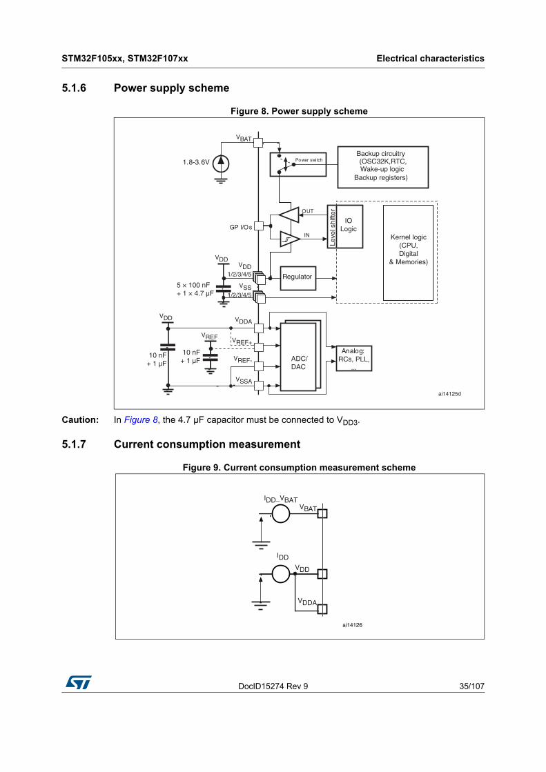
DocID15274 Rev 9 35/107
STM32F105xx, STM32F107xx Electrical characteristics
106
5.1.6 Power supply scheme
Figure 8. Power supply scheme
Caution: In Figure 8, the 4.7 µF capacitor must be connected to VDD3.
5.1.7 Current consumption measurement
Figure 9. Current consumption measurement scheme
ai14125d
VDD1/2/3/4/5
Analog: RCs, PLL,
...
Power switch
VBAT
GP I/Os
OUT
IN Kernel logic (CPU, Digital
& Memories)
Backup circuitry(OSC32K,RTC,
Backup registers)Wake-up logic
5 × 100 nF+ 1 × 4.7 µF
1.8-3.6V
RegulatorVSS
1/2/3/4/5
VDDA
VREF+
VREF-
VSSA
ADC/DAC
Leve
l shi
fter
IOLogic
VDD
10 nF+ 1 µF
VREF
10 nF+ 1 µF
VDD
ai14126
VBAT
VDD
VDDA
IDD_VBAT
IDD

Electrical characteristics STM32F105xx, STM32F107xx
36/107 DocID15274 Rev 9
5.2 Absolute maximum ratings
Stresses above the absolute maximum ratings listed in Table 6: Voltage characteristics, Table 7: Current characteristics, and Table 8: Thermal characteristics may cause permanent damage to the device. These are stress ratings only and functional operation of the device at these conditions is not implied. Exposure to maximum rating conditions for extended periods may affect device reliability.
Table 6. Voltage characteristics
Symbol Ratings Min Max Unit
VDD–VSSExternal main supply voltage (including VDDA and VDD)(1)
1. All main power (VDD, VDDA) and ground (VSS, VSSA) pins must always be connected to the external power supply, in the permitted range.
–0.3 4.0
V
VIN(2)
2. VIN maximum must always be respected. Refer to Table 7: Current characteristics for the maximum allowed injected current values.
Input voltage on five volt tolerant pin VSS − 0.3 VDD + 4.0
Input voltage on any other pin VSS − 0.3 4.0
|ΔVDDx| Variations between different VDD power pins - 50mV
|VSSX − VSS| Variations between all the different ground pins - 50
VESD(HBM)Electrostatic discharge voltage (human body model)
see Section 5.3.11: Absolute maximum ratings (electrical sensitivity)
-
Table 7. Current characteristics
Symbol Ratings Max. Unit
IVDD Total current into VDD/VDDA power lines (source)(1)
1. All main power (VDD, VDDA) and ground (VSS, VSSA) pins must always be connected to the external power supply, in the permitted range.
150
mA
IVSS Total current out of VSS ground lines (sink)(1) 150
IIOOutput current sunk by any I/O and control pin 25
Output current source by any I/Os and control pin − 25
IINJ(PIN)(2)
2. Negative injection disturbs the analog performance of the device. See Note: on page 76.
Injected current on five volt tolerant pins(3)
3. Positive injection is not possible on these I/Os. A negative injection is induced by VIN<VSS. IINJ(PIN) must never be exceeded. Refer to Table 6: Voltage characteristics for the maximum allowed input voltage values.
-5/+0
Injected current on any other pin(4)
4. A positive injection is induced by VIN>VDD while a negative injection is induced by VIN<VSS. IINJ(PIN) must never be exceeded. Refer to Table 6: Voltage characteristics for the maximum allowed input voltage values.
± 5
ΣIINJ(PIN) Total injected current (sum of all I/O and control pins)(5)
5. When several inputs are submitted to a current injection, the maximum ΣIINJ(PIN) is the absolute sum of the positive and negative injected currents (instantaneous values).
± 25

DocID15274 Rev 9 37/107
STM32F105xx, STM32F107xx Electrical characteristics
106
5.3 Operating conditions
5.3.1 General operating conditions
Table 8. Thermal characteristics
Symbol Ratings Value Unit
TSTG Storage temperature range –65 to +150 °C
TJ Maximum junction temperature 150 °C
Table 9. General operating conditions
Symbol Parameter Conditions Min Max Unit
fHCLK Internal AHB clock frequency - 0 72
MHzfPCLK1 Internal APB1 clock frequency - 0 36
fPCLK2 Internal APB2 clock frequency - 0 72
VDD Standard operating voltage - 2 3.6 V
VDDA(1)
1. When the ADC is used, refer to Table 52: ADC characteristics.
Analog operating voltage(ADC not used) Must be the same potential
as VDD(2)
2. It is recommended to power VDD and VDDA from the same source. A maximum difference of 300 mV between VDD and VDDA can be tolerated during power-up and operation.
2 3.6
VAnalog operating voltage(ADC used)
2.4 3.6
VBAT Backup operating voltage - 1.8 3.6 V
PD
Power dissipation at TA = 85 °C for suffix 6 or TA = 105 °C for suffix 7(3)
3. If TA is lower, higher PD values are allowed as long as TJ does not exceed TJmax.
LFBGA100 - 500
mWLQFP100 - 434
LQFP64 - 444
PD
Power dissipation at TA = 85 °C for suffix 6 or TA = 105 °C for suffix 7(4)
4. If TA is lower, higher PD values are allowed as long as TJ does not exceed TJmax.
LQFP100 - 434mW
LQFP64 - 444
TA
Ambient temperature for 6 suffix version
Maximum power dissipation –40 85°C
Low power dissipation(5)
5. In low power dissipation state, TA can be extended to this range as long as TJ does not exceed TJmax.
–40 105
Ambient temperature for 7 suffix version
Maximum power dissipation –40 105°C
Low power dissipation(5) –40 125
TJ Junction temperature range6 suffix version –40 105
°C7 suffix version –40 125

Electrical characteristics STM32F105xx, STM32F107xx
38/107 DocID15274 Rev 9
5.3.2 Operating conditions at power-up / power-down
Subject to general operating conditions for TA.
5.3.3 Embedded reset and power control block characteristics
The parameters given in Table 11 are derived from tests performed under ambient temperature and VDD supply voltage conditions summarized in Table 9.
Table 10. Operating condition at power-up / power down
Symbol Parameter Condition Min Max Unit
tVDD VDD rise time rate-
0 -µs/V
TJ VDD fall time rate 20 -
Table 11. Embedded reset and power control block characteristics
Symbol Parameter Conditions Min Typ Max Unit
VPVDProgrammable voltage detector level selection
PLS[2:0]=000 (rising edge) 2.1 2.18 2.26 V
PLS[2:0]=000 (falling edge) 2 2.08 2.16 V
PLS[2:0]=001 (rising edge) 2.19 2.28 2.37 V
PLS[2:0]=001 (falling edge) 2.09 2.18 2.27 V
PLS[2:0]=010 (rising edge) 2.28 2.38 2.48 V
PLS[2:0]=010 (falling edge) 2.18 2.28 2.38 V
PLS[2:0]=011 (rising edge) 2.38 2.48 2.58 V
PLS[2:0]=011 (falling edge) 2.28 2.38 2.48 V
PLS[2:0]=100 (rising edge) 2.47 2.58 2.69 V
PLS[2:0]=100 (falling edge) 2.37 2.48 2.59 V
PLS[2:0]=101 (rising edge) 2.57 2.68 2.79 V
PLS[2:0]=101 (falling edge) 2.47 2.58 2.69 V
PLS[2:0]=110 (rising edge) 2.66 2.78 2.9 V
PLS[2:0]=110 (falling edge) 2.56 2.68 2.8 V
PLS[2:0]=111 (rising edge) 2.76 2.88 3 V
PLS[2:0]=111 (falling edge) 2.66 2.78 2.9 V
VPVDhyst(2) PVD hysteresis - - 100 - mV
VPOR/PDRPower on/power down reset threshold
Falling edge 1.8(1)
1. The product behavior is guaranteed by design down to the minimum VPOR/PDR value.
1.88 1.96 V
Rising edge 1.84 1.92 2.0 V
VPDRhyst(2) PDR hysteresis - - 40 - mV
TRSTTEMPO(2)
2. Guaranteed by design, not tested in production.
Reset temporization - 1 2.5 4.5 ms

DocID15274 Rev 9 39/107
STM32F105xx, STM32F107xx Electrical characteristics
106
5.3.4 Embedded reference voltage
The parameters given in Table 12 are derived from tests performed under ambient temperature and VDD supply voltage conditions summarized in Table 9.
5.3.5 Supply current characteristics
The current consumption is a function of several parameters and factors such as the operating voltage, ambient temperature, I/O pin loading, device software configuration, operating frequencies, I/O pin switching rate, program location in memory and executed binary code.The current consumption is measured as described in Figure 9: Current consumption measurement scheme.All Run-mode current consumption measurements given in this section are performed with a reduced code that gives a consumption equivalent to Dhrystone 2.1 code.
Maximum current consumption
The MCU is placed under the following conditions:
• All I/O pins are in input mode with a static value at VDD or VSS (no load)
• All peripherals are disabled except when explicitly mentioned
• The Flash memory access time is adjusted to the fHCLK frequency (0 wait state from 0 to 24 MHz, 1 wait state from 24 to 48 MHz and 2 wait states above)
• Prefetch in ON (reminder: this bit must be set before clock setting and bus prescaling)
• When the peripherals are enabled fPCLK1 = fHCLK/2, fPCLK2 = fHCLK
The parameters given in Table 13, Table 14 and Table 15 are derived from tests performed under ambient temperature and VDD supply voltage conditions summarized in Table 9.
Table 12. Embedded internal reference voltage
Symbol Parameter Conditions Min Typ Max Unit
VREFINT Internal reference voltage–40 °C < TA < +105 °C 1.16 1.20 1.26 V
–40 °C < TA < +85 °C 1.16 1.20 1.24 V
TS_vrefint(1)
1. Shortest sampling time can be determined in the application by multiple iterations.
ADC sampling time when reading the internal reference voltage
- - 5.1 17.1(2)
2. Guaranteed by design, not tested in production.
µs
VRERINT(2)
Internal reference voltage spread over the temperature range
VDD = 3 V ±10 mV - - 10 mV
TCoeff(2) Temperature coefficient - - - 100 ppm/°C

Electrical characteristics STM32F105xx, STM32F107xx
40/107 DocID15274 Rev 9
Table 13. Maximum current consumption in Run mode, code with data processingrunning from Flash
Symbol Parameter Conditions fHCLK
Max(1)
1. Based on characterization, not tested in production.
UnitTA = 85 °C TA = 105 °C
IDDSupply current in Run mode
External clock(2), all peripherals enabled
2. External clock is 8 MHz and PLL is on when fHCLK > 8 MHz.
72 MHz 68 68.4
mA
48 MHz 49 49.2
36 MHz 38.7 38.9
24 MHz 27.3 27.9
16 MHz 20.2 20.5
8 MHz 10.2 10.8
External clock(2), all peripherals disabled
72 MHz 32.7 32.9
48 MHz 25 25.2
36 MHz 20.3 20.6
24 MHz 14.8 15.1
16 MHz 11.2 11.7
8 MHz 6.6 7.2
Table 14. Maximum current consumption in Run mode, code with data processingrunning from RAM
Symbol Parameter Conditions fHCLK
Max(1)
1. Based on characterization, tested in production at VDD max, fHCLK max..
UnitTA = 85 °C TA = 105 °C
IDD
Supply current in Run mode
External clock(2), all peripherals enabled
2. External clock is 8 MHz and PLL is on when fHCLK > 8 MHz.
72 MHz 65.5 66
mA
48 MHz 45.4 46
36 MHz 35.5 36.1
24 MHz 25.2 25.6
16 MHz 18 18.5
8 MHz 10.5 11
External clock(2), all peripherals disabled
72 MHz 31.4 31.9
48 MHz 27.8 28.2
36 MHz 17.6 18.3
24 MHz 13.1 13.8
16 MHz 10.2 10.9
8 MHz 6.1 7.8

DocID15274 Rev 9 41/107
STM32F105xx, STM32F107xx Electrical characteristics
106
Table 15. Maximum current consumption in Sleep mode, code running from Flash or RAM
Symbol Parameter Conditions fHCLK
Max(1)
UnitTA = 85 °C TA = 105 °C
IDDSupply current in Sleep mode
External clock(2), all peripherals enabled
72 MHz 48.4 49
mA
48 MHz 33.9 34.4
36 MHz 26.7 27.2
24 MHz 19.3 19.8
16 MHz 14.2 14.8
8 MHz 8.7 9.1
External clock(2), all peripherals disabled
72 MHz 10.1 10.6
48 MHz 8.3 8.75
36 MHz 7.5 8
24 MHz 6.6 7.1
16 MHz 6 6.5
8 MHz 2.5 3
1. Based on characterization, tested in production at VDD max and fHCLK max with peripherals enabled.
2. External clock is 8 MHz and PLL is on when fHCLK > 8 MHz.
Table 16. Typical and maximum current consumptions in Stop and Standby modes
Symbol Parameter Conditions
Typ(1) Max
UnitVDD/VBAT = 2.0 V
VDD/VBAT = 2.4 V
VDD/VBAT = 3.3 V
TA = 85 °C
TA = 105 °C
IDD
Supply current in Stop mode
Regulator in Run mode, low-speed and high-speed internal RC oscillators and high-speed oscillator OFF (no independent watchdog)
- 32 33 600 1300
µA
Regulator in Low Power mode, low-speed and high-speed internal RC oscillators and high-speed oscillator OFF (no independent watchdog)
- 25 26 590 1280
Supply current in Standby mode
Low-speed internal RC oscillator and independent watchdog ON
- 3 3.8 - -
Low-speed internal RC oscillator ON, independent watchdog OFF
- 2.8 3.6 - -
Low-speed internal RC oscillator and independent watchdog OFF, low-speed oscillator and RTC OFF
- 1.9 2.1 5(2) 6.5(2)
IDD_VBAT
Backup domain supply current
Low-speed oscillator and RTC ON 1.1 1.2 1.4 2.1(2) 2.3(2)
1. Typical values are measured at TA = 25 °C.
2. Based on characterization, not tested in production.
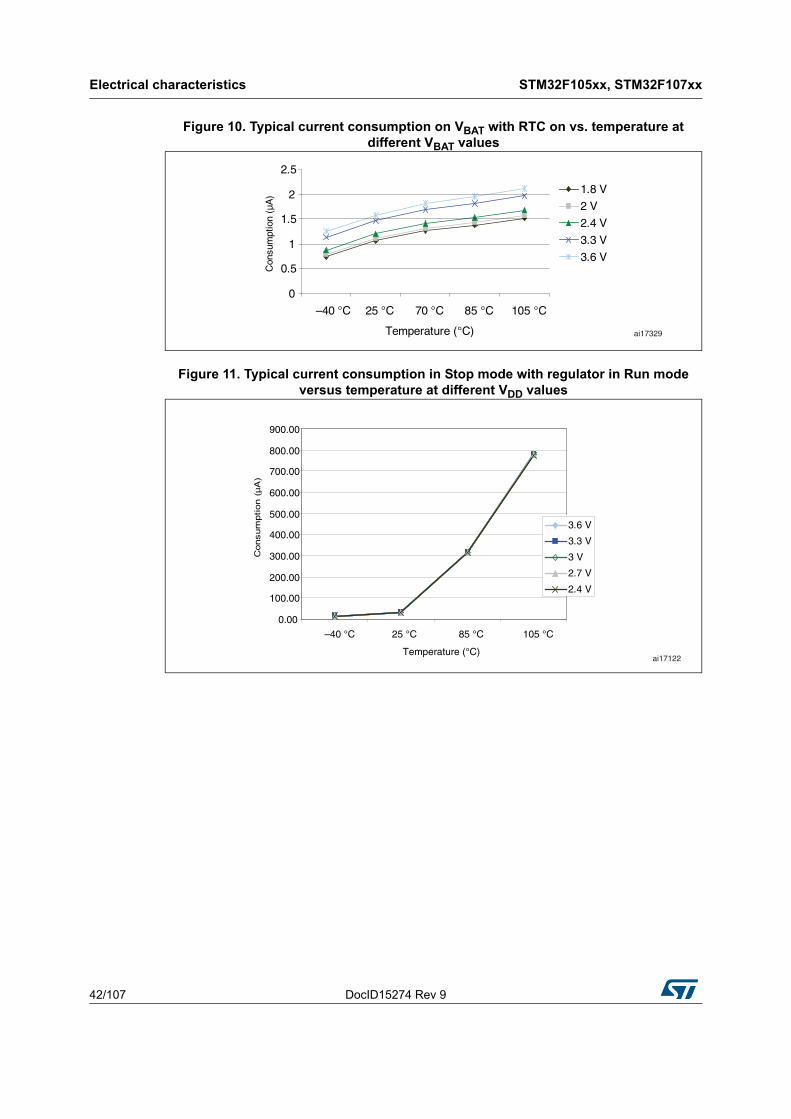
Electrical characteristics STM32F105xx, STM32F107xx
42/107 DocID15274 Rev 9
Figure 10. Typical current consumption on VBAT with RTC on vs. temperature atdifferent VBAT values
Figure 11. Typical current consumption in Stop mode with regulator in Run modeversus temperature at different VDD values
0
0.5
1
1.5
2
2.5
–40 °C 25 °C 70 °C 85 °C 105 °C
Temperature (°C)
Con
sum
ptio
n (µ
A)
1.8 V
2 V
2.4 V
3.3 V
3.6 V
ai17329
0.00
100.00
200.00
300.00
400.00
500.00
600.00
700.00
800.00
900.00
–40 °C 25 °C 85 °C 105 °C
Temperature (°C)
Consum
ption (
µA
)
3.6 V
3.3 V
3 V
2.7 V
2.4 V
ai17122

DocID15274 Rev 9 43/107
STM32F105xx, STM32F107xx Electrical characteristics
106
Figure 12. Typical current consumption in Stop mode with regulator in Low-powermode versus temperature at different VDD values
Figure 13. Typical current consumption in Standby mode versus temperature atdifferent VDD values
Typical current consumption
The MCU is placed under the following conditions:
• All I/O pins are in input mode with a static value at VDD or VSS (no load).
• All peripherals are disabled except if it is explicitly mentioned.
• The Flash access time is adjusted to fHCLK frequency (0 wait state from 0 to 24 MHz, 1 wait state from 24 to 48 MHz and 2 wait states above).
• Ambient temperature and VDD supply voltage conditions summarized in Table 9.
• Prefetch is ON (Reminder: this bit must be set before clock setting and bus prescaling)
When the peripherals are enabled fPCLK1 = fHCLK/4, fPCLK2 = fHCLK/2, fADCCLK = fPCLK2/4
0.00
100.00
200.00
300.00
400.00
500.00
600.00
700.00
800.00
900.00
–40 °C 25 °C 85 °C 105 °C
Temperature (°C)
Co
nsu
mp
tio
n (
µA
)
3.6 V
3.3 V
3 V
2.7 V
2.4 V
ai17123
0.00
0.50
1.00
1.50
2.00
2.50
3.00
3.50
4.00
4.50
–40 °C 25 °C 85 °C 105 °C
Temperature (°C)
Co
nsu
mp
tio
n (
µA
)
3.6 V
3.3 V
3 V
2.7 V
2.4 V
ai17124
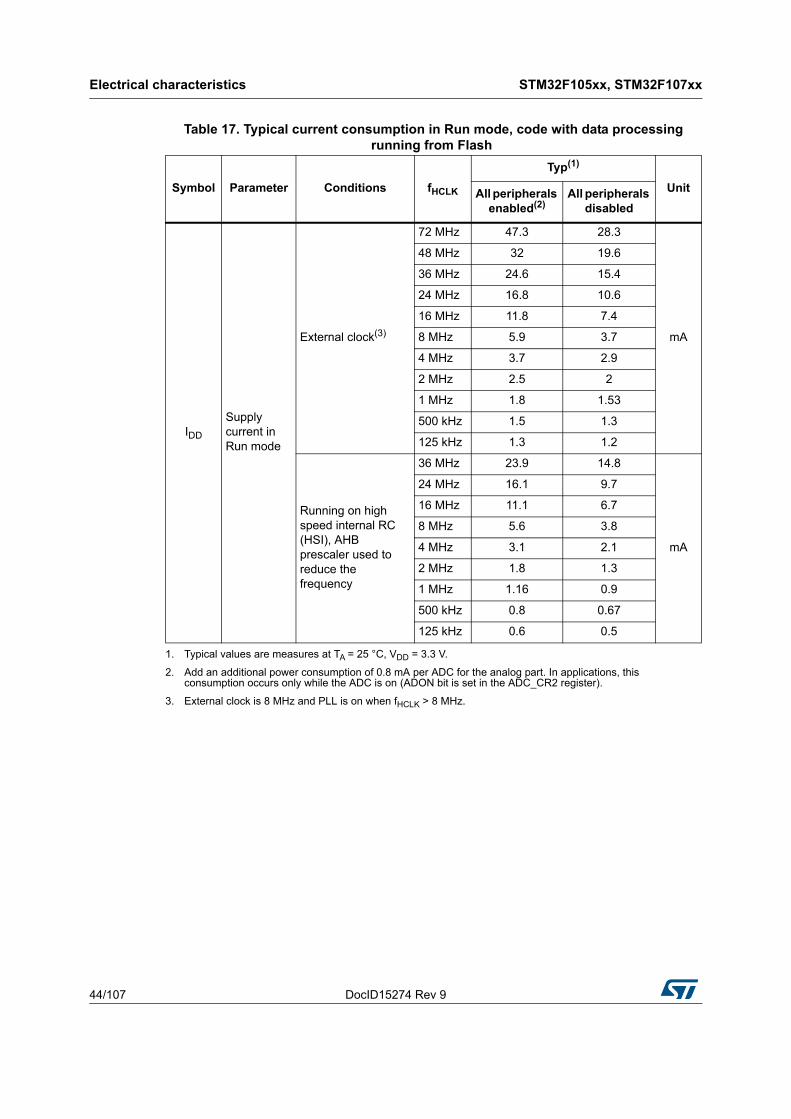
Electrical characteristics STM32F105xx, STM32F107xx
44/107 DocID15274 Rev 9
Table 17. Typical current consumption in Run mode, code with data processingrunning from Flash
Symbol Parameter Conditions fHCLK
Typ(1)
1. Typical values are measures at TA = 25 °C, VDD = 3.3 V.
UnitAll peripherals enabled(2)
2. Add an additional power consumption of 0.8 mA per ADC for the analog part. In applications, this consumption occurs only while the ADC is on (ADON bit is set in the ADC_CR2 register).
All peripherals disabled
IDD
Supply current in Run mode
External clock(3)
3. External clock is 8 MHz and PLL is on when fHCLK > 8 MHz.
72 MHz 47.3 28.3
mA
48 MHz 32 19.6
36 MHz 24.6 15.4
24 MHz 16.8 10.6
16 MHz 11.8 7.4
8 MHz 5.9 3.7
4 MHz 3.7 2.9
2 MHz 2.5 2
1 MHz 1.8 1.53
500 kHz 1.5 1.3
125 kHz 1.3 1.2
Running on high speed internal RC (HSI), AHB prescaler used to reduce the frequency
36 MHz 23.9 14.8
mA
24 MHz 16.1 9.7
16 MHz 11.1 6.7
8 MHz 5.6 3.8
4 MHz 3.1 2.1
2 MHz 1.8 1.3
1 MHz 1.16 0.9
500 kHz 0.8 0.67
125 kHz 0.6 0.5
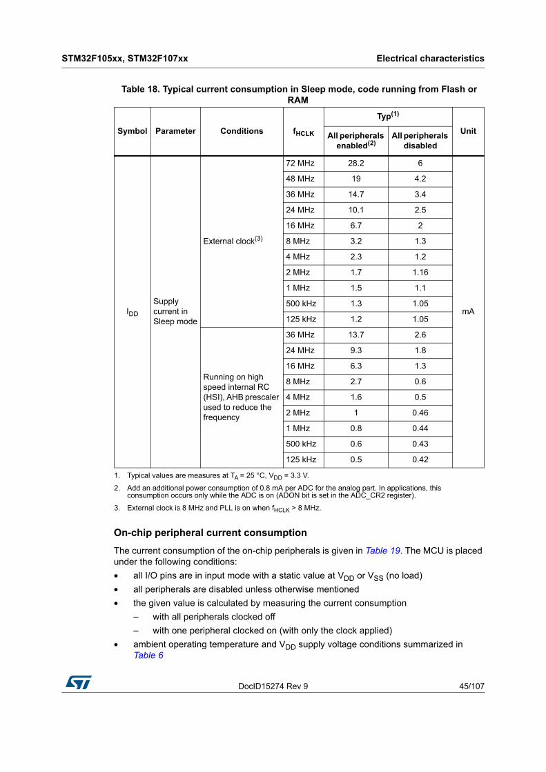
DocID15274 Rev 9 45/107
STM32F105xx, STM32F107xx Electrical characteristics
106
On-chip peripheral current consumption
The current consumption of the on-chip peripherals is given in Table 19. The MCU is placed under the following conditions:
• all I/O pins are in input mode with a static value at VDD or VSS (no load)
• all peripherals are disabled unless otherwise mentioned
• the given value is calculated by measuring the current consumption
– with all peripherals clocked off
– with one peripheral clocked on (with only the clock applied)
• ambient operating temperature and VDD supply voltage conditions summarized in Table 6
Table 18. Typical current consumption in Sleep mode, code running from Flash orRAM
Symbol Parameter Conditions fHCLK
Typ(1)
1. Typical values are measures at TA = 25 °C, VDD = 3.3 V.
UnitAll peripherals enabled(2)
2. Add an additional power consumption of 0.8 mA per ADC for the analog part. In applications, this consumption occurs only while the ADC is on (ADON bit is set in the ADC_CR2 register).
All peripherals disabled
IDD
Supply current in Sleep mode
External clock(3)
3. External clock is 8 MHz and PLL is on when fHCLK > 8 MHz.
72 MHz 28.2 6
mA
48 MHz 19 4.2
36 MHz 14.7 3.4
24 MHz 10.1 2.5
16 MHz 6.7 2
8 MHz 3.2 1.3
4 MHz 2.3 1.2
2 MHz 1.7 1.16
1 MHz 1.5 1.1
500 kHz 1.3 1.05
125 kHz 1.2 1.05
Running on high speed internal RC (HSI), AHB prescaler used to reduce the frequency
36 MHz 13.7 2.6
24 MHz 9.3 1.8
16 MHz 6.3 1.3
8 MHz 2.7 0.6
4 MHz 1.6 0.5
2 MHz 1 0.46
1 MHz 0.8 0.44
500 kHz 0.6 0.43
125 kHz 0.5 0.42

Electrical characteristics STM32F105xx, STM32F107xx
46/107 DocID15274 Rev 9
Table 19. Peripheral current consumption
Peripheral Typical consumption at 25 °C Unit
AHB (up to 72 MHz)
DMA1 14.03
µA/MHz
DMA2 9.31
OTG_fs 111.11
ETH-MAC 56.25
CRC 1.11
BusMatrix(1) 15.97
APB1(up to 36MHz)
APB1-Bridge 9.72
µA/MHz
TIM2 33.61
TIM3 33.06
TIM4 32.50
TIM5 31.94
TIM6 6.11
TIM7 6.11
SPI2/I2S2(2) 7.50
SPI3/I2S3(2) 7.50
USART2 10.83
USART3 11.11
UART4 10.83
UART5 10.56
I2C1 11.39
I2C2 11.11
CAN1 19.44
CAN2 18.33
DAC(3) 8.61
WWDG 3.33
PWR 2.22
BKP 0.83
IWDG 3.89

DocID15274 Rev 9 47/107
STM32F105xx, STM32F107xx Electrical characteristics
106
5.3.6 External clock source characteristics
High-speed external user clock generated from an external source
The characteristics given in Table 20 result from tests performed using an high-speed external clock source, and under ambient temperature and supply voltage conditions summarized in Table 9.
APB2 (up to 72 MHz)
APB2-Bridge 3.47
µA/MHz
GPIOA 6.39
GPIOB 6.39
GPIOC 6.11
GPIOD 6.39
GPIOE 6.11
SPI1 3.61
USART1 12.08
TIM1 23.47
ADC1(4) 18.21
1. The BusMatrix is automatically active when at least one master is ON.(CPU, ETH-MAC, DMA1 or DMA2).
2. When I2S is enabled we have a consumption add equal to 0, 02 mA.
3. When DAC_OUT1 or DAC_OUT2 is enabled we have a consumption add equal to 0, 3 mA.
4. Specific conditions for measuring ADC current consumption: fHCLK = 56 MHz, fAPB1 = fHCLK/2, fAPB2 = fHCLK, fADCCLK = fAPB2/4. When ADON bit in the ADC_CR2 register is set to 1, a current consumption of analog part equal to 0.6 mA must be added.
Table 19. Peripheral current consumption (continued)
Peripheral Typical consumption at 25 °C Unit
Table 20. High-speed external user clock characteristics
Symbol Parameter Conditions Min Typ Max Unit
fHSE_extExternal user clock source frequency(1)
-
1 8 50 MHz
VHSEH OSC_IN input pin high level voltage 0.7VDD - VDDV
VHSEL OSC_IN input pin low level voltage VSS - 0.3VDD
tw(HSE)tw(HSE)
OSC_IN high or low time(1)
1. Guaranteed by design, not tested in production.
5 - -
nstr(HSE)tf(HSE)
OSC_IN rise or fall time(1) - - 20
Cin(HSE) OSC_IN input capacitance(1) - - 5 - pF
DuCy(HSE) Duty cycle - 45 - 55 %
IL OSC_IN Input leakage current VSS ≤VIN ≤VDD - - ±1 µA

Electrical characteristics STM32F105xx, STM32F107xx
48/107 DocID15274 Rev 9
Low-speed external user clock generated from an external source
The characteristics given in Table 21 result from tests performed using an low-speed external clock source, and under ambient temperature and supply voltage conditions summarized in Table 9.
Figure 14. High-speed external clock source AC timing diagram
Table 21. Low-speed external user clock characteristics
Symbol Parameter Conditions Min Typ Max Unit
fLSE_extUser External clock source frequency(1)
1. Guaranteed by design, not tested in production.
-
32.768 1000 kHz
VLSEHOSC32_IN input pin high level voltage
0.7VDD - VDD
V
VLSELOSC32_IN input pin low level voltage
VSS - 0.3VDD
tw(LSE)tw(LSE)
OSC32_IN high or low time(1) 450 - -
nstr(LSE)tf(LSE)
OSC32_IN rise or fall time(1) - - 50
Cin(LSE) OSC32_IN input capacitance(1) - - 5 pF
DuCy(LSE) Duty cycle - 30 - 70 %
IL OSC32_IN Input leakage current VSS ≤VIN ≤VDD - - ±1 µA

DocID15274 Rev 9 49/107
STM32F105xx, STM32F107xx Electrical characteristics
106
Figure 15. Low-speed external clock source AC timing diagram
High-speed external clock generated from a crystal/ceramic resonator
The high-speed external (HSE) clock can be supplied with a 3 to 25 MHz crystal/ceramic resonator oscillator. All the information given in this paragraph are based on characterization results obtained with typical external components specified in Table 22. In the application, the resonator and the load capacitors have to be placed as close as possible to the oscillator pins in order to minimize output distortion and startup stabilization time. Refer to the crystal resonator manufacturer for more details on the resonator characteristics (frequency, package, accuracy).
Table 22. HSE 3-25 MHz oscillator characteristics(1) (2)
1. Resonator characteristics given by the crystal/ceramic resonator manufacturer.
2. Based on characterization, not tested in production.
Symbol Parameter Conditions Min Typ Max Unit
fOSC_IN Oscillator frequency - 3 25 MHz
RF Feedback resistor - - 200 - kΩ
CRecommended load capacitance versus equivalent serial resistance of the crystal (RS)(3)
3. The relatively low value of the RF resistor offers a good protection against issues resulting from use in a humid environment, due to the induced leakage and the bias condition change. However, it is recommended to take this point into account if the MCU is used in tough humidity conditions.
RS = 30 Ω - 30 - pF
i2 HSE driving currentVDD = 3.3 V, VIN = VSS
with 30 pF load - - 1 mA
gm Oscillator transconductance Startup 25 - - mA/V
tSU(HSE(4)
4. tSU(HSE) is the startup time measured from the moment it is enabled (by software) to a stabilized 8 MHz oscillation is reached. This value is measured for a standard crystal resonator and it can vary significantly with the crystal manufacturer
Startup time VDD is stabilized - 2 - ms
ai14140c
OSC32_INExternal
STM32F10xxx
clock source
VLSEH
tf(LSE) tW(LSE)
IL
90%
10%
TLSE
ttr(LSE)tW(LSE)
fLSE_ext
VLSEL

Electrical characteristics STM32F105xx, STM32F107xx
50/107 DocID15274 Rev 9
For CL1 and CL2, it is recommended to use high-quality external ceramic capacitors in the 5 pF to 25 pF range (typ.), designed for high-frequency applications, and selected to match the requirements of the crystal or resonator (see Figure 16). CL1 and CL2 are usually the same size. The crystal manufacturer typically specifies a load capacitance which is the series combination of CL1 and CL2. PCB and MCU pin capacitance must be included (10 pF can be used as a rough estimate of the combined pin and board capacitance) when sizing CL1 and CL2. Refer to the application note AN2867 “Oscillator design guide for ST microcontrollers” available from the ST website www.st.com.
Figure 16. Typical application with an 8 MHz crystal
1. REXT value depends on the crystal characteristics.
Low-speed external clock generated from a crystal/ceramic resonator
The low-speed external (LSE) clock can be supplied with a 32.768 kHz crystal/ceramic resonator oscillator. All the information given in this paragraph are based on characterization results obtained with typical external components specified in Table 23. In the application, the resonator and the load capacitors have to be placed as close as possible to the oscillator pins in order to minimize output distortion and startup stabilization time. Refer to the crystal resonator manufacturer for more details on the resonator characteristics (frequency, package, accuracy).
Table 23. LSE oscillator characteristics (fLSE = 32.768 kHz) (1)
Symbol Parameter Conditions Min Typ Max Unit
RF Feedback resistor - - 5 - MΩ
C(2)Recommended load capacitance versus equivalent serial resistance of the crystal (RS)(3)
RS = 30 kΩ - - 15 pF
I2 LSE driving current VDD = 3.3 V, VIN = VSS - - 1.4 µA
gm Oscillator Transconductance - 5 - - µA/V

DocID15274 Rev 9 51/107
STM32F105xx, STM32F107xx Electrical characteristics
106
Note: For CL1 and CL2 it is recommended to use high-quality external ceramic capacitors in the 5 pF to 15 pF range selected to match the requirements of the crystal or resonator (see Figure 17). CL1 and CL2, are usually the same size. The crystal manufacturer typically specifies a load capacitance which is the series combination of CL1 and CL2.Load capacitance CL has the following formula: CL = CL1 x CL2 / (CL1 + CL2) + Cstray where Cstray is the pin capacitance and board or trace PCB-related capacitance. Typically, it is between 2 pF and 7 pF.
Caution: To avoid exceeding the maximum value of CL1 and CL2 (15 pF) it is strongly recommended to use a resonator with a load capacitance CL ≤ 7 pF. Never use a resonator with a load capacitance of 12.5 pF.Example: if you choose a resonator with a load capacitance of CL = 6 pF, and Cstray = 2 pF, then CL1 = CL2 = 8 pF.
Figure 17. Typical application with a 32.768 kHz crystal
tSU(LSE)(4) Startup time VDD is stabilized
TA = 50 °C - 1.5 -
s
TA = 25 °C - 2.5 -
TA = 10 °C - 4 -
TA = 0 °C - 6 -
TA = -10 °C - 10 -
TA = -20 °C - 17 -
TA = -30 °C - 32 -
TA = -40 °C - 60 -
1. Based on characterization, not tested in production.
2. Refer to the note and caution paragraphs below the table, and to the application note AN2867 “Oscillator design guide for ST microcontrollers”.
3. The oscillator selection can be optimized in terms of supply current using an high quality resonator with small RS value for example MSIV-TIN32.768kHz. Refer to crystal manufacturer for more details
4. tSU(LSE) is the startup time measured from the moment it is enabled (by software) to a stabilized 32.768 kHz oscillation is reached. This value is measured for a standard crystal and it can vary significantly with the crystal manufacturer
Table 23. LSE oscillator characteristics (fLSE = 32.768 kHz) (1) (continued)
Symbol Parameter Conditions Min Typ Max Unit

Electrical characteristics STM32F105xx, STM32F107xx
52/107 DocID15274 Rev 9
5.3.7 Internal clock source characteristics
The parameters given in Table 24 are derived from tests performed under ambient temperature and VDD supply voltage conditions summarized in Table 9.
High-speed internal (HSI) RC oscillator
Low-speed internal (LSI) RC oscillator
Wakeup time from low-power mode
The wakeup times given in Table 26 is measured on a wakeup phase with a 8-MHz HSI RC oscillator. The clock source used to wake up the device depends from the current operating mode:
• Stop or Standby mode: the clock source is the RC oscillator
• Sleep mode: the clock source is the clock that was set before entering Sleep mode.
Table 24. HSI oscillator characteristics (1)
1. VDD = 3.3 V, TA = –40 to 105 °C unless otherwise specified.
Symbol Parameter Conditions Min Typ Max Unit
fHSI Frequency - - 8 MHz
DuCy(HSI) Duty cycle - 45 - 55 %
ACCHSIAccuracy of the HSI oscillator
User-trimmed with the RCC_CR register(2)
2. Refer to application note AN2868 “STM32F10xxx internal RC oscillator (HSI) calibration” available from the ST website www.st.com.
- - 1(3)
3. Guaranteed by design, not tested in production.
%
Factory-calibrated(4)
4. Based on characterization, not tested in production.
TA = –40 to 105 °C –2 - 2.5 %
TA = –10 to 85 °C –1.5 - 2.2 %
TA = 0 to 70 °C –1.3 - 2 %
TA = 25 °C –1.1 - 1.8 %
tsu(HSI)(4) HSI oscillator
startup time- 1 - 2 µs
IDD(HSI)(4) HSI oscillator
power consumption- - 80 100 µA
Table 25. LSI oscillator characteristics (1)
1. VDD = 3 V, TA = –40 to 105 °C unless otherwise specified.
Symbol Parameter Min Typ Max Unit
fLSI(2)
2. Based on characterization, not tested in production.
Frequency 30 40 60 kHz
tsu(LSI)(3)
3. Guaranteed by design, not tested in production.
LSI oscillator startup time - - 85 µs
IDD(LSI)(3) LSI oscillator power consumption - 0.65 1.2 µA

DocID15274 Rev 9 53/107
STM32F105xx, STM32F107xx Electrical characteristics
106
All timings are derived from tests performed under ambient temperature and VDD supply voltage conditions summarized in Table 9.
5.3.8 PLL, PLL2 and PLL3 characteristics
The parameters given in Table 27 and Table 28 are derived from tests performed under temperature and VDD supply voltage conditions summarized in Table 9.
Table 26. Low-power mode wakeup timings
Symbol Parameter Typ Unit
tWUSLEEP(1)
1. The wakeup times are measured from the wakeup event to the point in which the user application code reads the first instruction.
Wakeup from Sleep mode 1.8 µs
tWUSTOP(1)
Wakeup from Stop mode (regulator in run mode) 3.6µs
Wakeup from Stop mode (regulator in low power mode) 5.4
tWUSTDBY(1) Wakeup from Standby mode 50 µs
Table 27. PLL characteristics
Symbol Parameter Min(1)
1. Based on characterization, not tested in production.
Max(1) Unit
fPLL_IN
PLL input clock(2)
2. Take care of using the appropriate multiplier factors so as to have PLL input clock values compatible with the range defined by fPLL_OUT.
3 12 MHz
Pulse width at high level 30 - ns
fPLL_OUT PLL multiplier output clock 18 72 MHz
fVCO_OUT PLL VCO output 36 144 MHz
tLOCK PLL lock time - 350 µs
Jitter Cycle-to-cycle jitter - 300 ps
Table 28. PLL2 and PLL3 characteristics
Symbol Parameter Min(1)
1. Based on characterization, not tested in production.
Max(1) Unit
fPLL_IN
PLL input clock(2)
2. Take care of using the appropriate multiplier factors so as to have PLL input clock values compatible with the range defined by fPLL_OUT.
3 5 MHz
Pulse width at high level 30 - ns
fPLL_OUT PLL multiplier output clock 40 74 MHz
fVCO_OUT PLL VCO output 80 148 MHz
tLOCK PLL lock time - 350 µs
Jitter Cycle-to-cycle jitter - 400 ps

Electrical characteristics STM32F105xx, STM32F107xx
54/107 DocID15274 Rev 9
5.3.9 Memory characteristics
Flash memory
The characteristics are given at TA = –40 to 105 °C unless otherwise specified.
5.3.10 EMC characteristics
Susceptibility tests are performed on a sample basis during device characterization.
Functional EMS (electromagnetic susceptibility)
While a simple application is executed on the device (toggling 2 LEDs through I/O ports). the device is stressed by two electromagnetic events until a failure occurs. The failure is indicated by the LEDs:
• Electrostatic discharge (ESD) (positive and negative) is applied to all device pins until a functional disturbance occurs. This test is compliant with the IEC 61000-4-2 standard.
• FTB: A burst of fast transient voltage (positive and negative) is applied to VDD and VSS through a 100 pF capacitor, until a functional disturbance occurs. This test is compliant with the IEC 61000-4-4 standard.
Table 29. Flash memory characteristics
Symbol Parameter Conditions Min(1) Typ Max(1)
1. Guaranteed by design, not tested in production.
Unit
tprog 16-bit programming time TA = –40 to +105 °C 40 52.5 70 µs
tERASE Page (1 KB) erase time TA = –40 to +105 °C 20 - 40 ms
tME Mass erase time TA = –40 to +105 °C 20 - 40 ms
IDD Supply current
Read modefHCLK = 72 MHz with 2 wait states, VDD = 3.3 V
- - 20 mA
Write / Erase modes fHCLK = 72 MHz, VDD = 3.3 V
- - 5 mA
Power-down mode / Halt,VDD = 3.0 to 3.6 V
- - 50 µA
Vprog Programming voltage - 2 - 3.6 V
Table 30. Flash memory endurance and data retention
Symbol Parameter Conditions Min(1) Typ Max(1)
1. Based on characterization, not tested in production.
Unit
NEND EnduranceTA = –40 to +85 °C (6 suffix versions)
TA = –40 to +105 °C (7 suffix versions)10 - - Kcycles
tRET Data retention
1 kcycle(2) at TA = 85 °C
2. Cycling performed over the whole temperature range.
30 - -
Years1 kcycle(2) at TA = 105 °C 10 - -
10 kcycles(2) at TA = 55 °C 20 - -

DocID15274 Rev 9 55/107
STM32F105xx, STM32F107xx Electrical characteristics
106
A device reset allows normal operations to be resumed.
The test results are given in Table 31. They are based on the EMS levels and classes defined in application note AN1709.
Designing hardened software to avoid noise problems
EMC characterization and optimization are performed at component level with a typical application environment and simplified MCU software. It should be noted that good EMC performance is highly dependent on the user application and the software in particular.
Therefore it is recommended that the user applies EMC software optimization and prequalification tests in relation with the EMC level requested for his application.
Software recommendations
The software flowchart must include the management of runaway conditions such as:
• Corrupted program counter
• Unexpected reset
• Critical Data corruption (control registers...)
Prequalification trials
Most of the common failures (unexpected reset and program counter corruption) can be reproduced by manually forcing a low state on the NRST pin or the Oscillator pins for 1 second.
To complete these trials, ESD stress can be applied directly on the device, over the range of specification values. When unexpected behavior is detected, the software can be hardened to prevent unrecoverable errors occurring (see application note AN1015).
Electromagnetic Interference (EMI)
The electromagnetic field emitted by the device are monitored while a simple application is executed (toggling 2 LEDs through the I/O ports). This emission test is compliant with IEC61967-2 standard which specifies the test board and the pin loading.
Table 31. EMS characteristics
Symbol Parameter ConditionsLevel/Class
VFESDVoltage limits to be applied on any I/O pin to induce a functional disturbance
VDD = 3.3 V, LQFP100, TA = +25 °C, fHCLK = 72 MHz, conforms to IEC 61000-4-2
2B
VEFTB
Fast transient voltage burst limits to be applied through 100 pF on VDD and VSS pins to induce a functional disturbance
VDD = 3.3 V, LQFP100, TA = +25 °C, fHCLK = 72 MHz, conforms to IEC 61000-4-4
4A

Electrical characteristics STM32F105xx, STM32F107xx
56/107 DocID15274 Rev 9
5.3.11 Absolute maximum ratings (electrical sensitivity)
Based on three different tests (ESD, LU) using specific measurement methods, the device is stressed in order to determine its performance in terms of electrical sensitivity.
Electrostatic discharge (ESD)
Electrostatic discharges (a positive then a negative pulse separated by 1 second) are applied to the pins of each sample according to each pin combination. The sample size depends on the number of supply pins in the device (3 parts × (n+1) supply pins). This test conforms to the JESD22-A114/C101 standard.
Static latch-up
Two complementary static tests are required on six parts to assess the latch-up performance:
• A supply overvoltage is applied to each power supply pin
• A current injection is applied to each input, output and configurable I/O pin
These tests are compliant with EIA/JESD 78A IC latch-up standard.
5.3.12 I/O current injection characteristics
As a general rule, current injection to the I/O pins, due to external voltage below VSS or above VDD (for standard, 3 V-capable I/O pins) should be avoided during normal product
Table 32. EMI characteristics
Symbol Parameter ConditionsMonitored
frequency band
Max vs. [fHSE/fHCLK]Unit
8/48 MHz 8/72 MHz
SEMI Peak levelVDD = 3.3 V, TA = 25 °C,LQFP100 packagecompliant with IEC61967-2
0.1 to 30 MHz 9 9
dBµV30 to 130 MHz 26 13
130 MHz to 1GHz 25 31
EMI Level 4 4 -
Table 33. ESD absolute maximum ratings
Symbol Ratings Conditions ClassMaximum value(1) Unit
VESD(HBM)Electrostatic discharge voltage (human body model)
TA = +25 °C conforming to JESD22-A114
2 2000
V
VESD(CDM)Electrostatic discharge voltage (charge device model)
TA = +25 °C conforming to JESD22-C101
II 500
1. Based on characterization results, not tested in production.
Table 34. Electrical sensitivities
Symbol Parameter Conditions Class
LU Static latch-up class TA = +105 °C conforming to JESD78A II level A

DocID15274 Rev 9 57/107
STM32F105xx, STM32F107xx Electrical characteristics
106
operation. However, in order to give an indication of the robustness of the microcontroller in cases when abnormal injection accidentally happens, susceptibility tests are performed on a sample basis during device characterization.
Functional susceptibility to I/O current injection
While a simple application is executed on the device, the device is stressed by injecting current into the I/O pins programmed in floating input mode. While current is injected into the I/O pin, one at a time, the device is checked for functional failures.
The failure is indicated by an out of range parameter: ADC error above a certain limit (>5 LSB TUE), out of spec current injection on adjacent pins or other functional failure (for example reset, oscillator frequency deviation).
The test results are given in Table 35
5.3.13 I/O port characteristics
General input/output characteristics
Unless otherwise specified, the parameters given in Table 36 are derived from tests performed under the conditions summarized in Table 9. All I/Os are CMOS and TTL compliant.
Table 35. I/O current injection susceptibility
Symbol Description
Functional susceptibility
UnitNegative injection
Positive injection
IINJ
Injected current on OSC_IN32, OSC_OUT32, PA4, PA5, PC13
-0 +0
mAInjected current on all FT pins -5 +0
Injected current on any other pin -5 +5
Table 36. I/O static characteristics
Symbol Parameter Conditions Min Typ Max Unit
VIL
Standard IO input low level voltage
- –0.3 - 0.28*(VDD-2 V)+0.8 V V
IO FT(1) input low level voltage
- –0.3 - 0.32*(VDD-2V)+0.75 V V
VIH
Standard IO input high level voltage
- 0.41*(VDD-2 V)+1.3 V - VDD+0.3 V
IO FT(1) input high level voltage
VDD > 2 V0.42*(VDD-2 V)+1 V -
5.5 V
VDD ≤ 2 V 5.2
Vhys
Standard IO Schmitt trigger voltage hysteresis(2)
- 200 - - mV
IO FT Schmitt trigger voltage hysteresis(2) - 5% VDD
(3) - - mV

Electrical characteristics STM32F105xx, STM32F107xx
58/107 DocID15274 Rev 9
All I/Os are CMOS and TTL compliant (no software configuration required). Their characteristics cover more than the strict CMOS-technology or TTL parameters. The coverage of these requirements is shown in Figure 18 and Figure 19 for standard I/Os, and in Figure 20 and Figure 21 for 5 V tolerant I/Os.
Figure 18. Standard I/O input characteristics - CMOS port
Ilkg Input leakage current (4)
VSS ≤VIN ≤VDDStandard I/Os
- - ±1µA
VIN= 5 V, I/O FT - - 3
RPU
Weak pull-up equivalent resistor(5)
All pins except for PA10 VIN = VSS
30 40 50kΩ
PA10 8 11 15
RPD
Weak pull-down equivalent resistor(5)
All pins except for PA10 VIN = VDD
30 40 50kΩ
PA10 8 11 15
CIO I/O pin capacitance - - 5 - pF
1. FT = Five-volt tolerant. In order to sustain a voltage higher than VDD+0.3 the internal pull-up/pull-down resistors must be disabled.
2. Hysteresis voltage between Schmitt trigger switching levels. Based on characterization, not tested in production.
3. With a minimum of 100 mV.
4. Leakage could be higher than max. if negative current is injected on adjacent pins.
5. Pull-up and pull-down resistors are designed with a true resistance in series with a switchable PMOS/NMOS. This MOS/NMOS contribution to the series resistance is minimum (~10% order).
Table 36. I/O static characteristics (continued)
Symbol Parameter Conditions Min Typ Max Unit

DocID15274 Rev 9 59/107
STM32F105xx, STM32F107xx Electrical characteristics
106
Figure 19. Standard I/O input characteristics - TTL port
Figure 20. 5 V tolerant I/O input characteristics - CMOS port
Figure 21. 5 V tolerant I/O input characteristics - TTL port

Electrical characteristics STM32F105xx, STM32F107xx
60/107 DocID15274 Rev 9
Output driving current
The GPIOs (general purpose input/outputs) can sink or source up to +/-8 mA, and sink or source up to +/-20 mA (with a relaxed VOL/VOH).
In the user application, the number of I/O pins which can drive current must be limited to respect the absolute maximum rating specified in Section 5.2:
• The sum of the currents sourced by all the I/Os on VDD, plus the maximum Run consumption of the MCU sourced on VDD, cannot exceed the absolute maximum rating IVDD (see Table 7).
• The sum of the currents sunk by all the I/Os on VSS plus the maximum Run consumption of the MCU sunk on VSS cannot exceed the absolute maximum rating IVSS (see Table 7).
Output voltage levels
Unless otherwise specified, the parameters given in Table 37 are derived from tests performed under ambient temperature and VDD supply voltage conditions summarized in Table 9. All I/Os are CMOS and TTL compliant.
Table 37. Output voltage characteristics
Symbol Parameter Conditions Min Max Unit
VOL(1)
1. The IIO current sunk by the device must always respect the absolute maximum rating specified in Table 7 and the sum of IIO (I/O ports and control pins) must not exceed IVSS.
Output low level voltage for an I/O pin when 8 pins are sunk at same time TTL port
IIO = +8 mA
2.7 V < VDD < 3.6 V
- 0.4
V
VOH(2)
2. The IIO current sourced by the device must always respect the absolute maximum rating specified in Table 7 and the sum of IIO (I/O ports and control pins) must not exceed IVDD.
Output high level voltage for an I/O pin when 8 pins are sourced at same time
VDD–0.4 -
VOL (1) Output low level voltage for an I/O pin
when 8 pins are sunk at same time CMOS port
IIO =+ 8mA
2.7 V < VDD < 3.6 V
- 0.4
V
VOH (2) Output high level voltage for an I/O pin
when 8 pins are sourced at same time2.4 -
VOL(1)(3)
3. Based on characterization data, not tested in production.
Output low level voltage for an I/O pin when 8 pins are sunk at same time IIO = +20 mA
2.7 V < VDD < 3.6 V
- 1.3
V
VOH(2)(3) Output high level voltage for an I/O pin
when 8 pins are sourced at same timeVDD–1.3 -
VOL(1)(3) Output low level voltage for an I/O pin
when 8 pins are sunk at same time IIO = +6 mA
2 V < VDD < 2.7 V
- 0.4
V
VOH(2)(3) Output high level voltage for an I/O pin
when 8 pins are sourced at same timeVDD–0.4 -

DocID15274 Rev 9 61/107
STM32F105xx, STM32F107xx Electrical characteristics
106
Input/output AC characteristics
The definition and values of input/output AC characteristics are given in Figure 22 and Table 38, respectively.
Unless otherwise specified, the parameters given in Table 38 are derived from tests performed under the ambient temperature and VDD supply voltage conditions summarized in Table 9.
Table 38. I/O AC characteristics(1)
1. The I/O speed is configured using the MODEx[1:0] bits. Refer to the STM32F10xxx reference manual for a description of GPIO Port configuration register.
MODEx[1:0] bit value(1) Symbol Parameter Conditions Min Max Unit
10
fmax(IO)out Maximum frequency(2)
2. The maximum frequency is defined in Figure 22.
CL = 50 pF, VDD = 2 V to 3.6 V - 2 MHz
tf(IO)outOutput high to low level fall time
CL = 50 pF, VDD = 2 V to 3.6 V
- 125(3)
3. Guaranteed by design, not tested in production.
ns
tr(IO)outOutput low to high level rise time
- 125(3)
01
fmax(IO)out Maximum frequency(2) CL = 50 pF, VDD = 2 V to 3.6 V - 10 MHz
tf(IO)outOutput high to low level fall time
CL = 50 pF, VDD = 2 V to 3.6 V
- 25(3)
ns
tr(IO)outOutput low to high level rise time
- 25(3)
11
Fmax(IO)out Maximum frequency(2)
CL = 30 pF, VDD = 2.7 V to 3.6 V - 50 MHz
CL = 50 pF, VDD = 2.7 V to 3.6 V - 30 MHz
CL = 50 pF, VDD = 2 V to 2.7 V - 20 MHz
tf(IO)outOutput high to low level fall time
CL = 30 pF, VDD = 2.7 V to 3.6 V - 5(3)
ns
CL = 50 pF, VDD = 2.7 V to 3.6 V - 8(3)
CL = 50 pF, VDD = 2 V to 2.7 V - 12(3)
tr(IO)outOutput low to high level rise time
CL = 30 pF, VDD = 2.7 V to 3.6 V - 5(3)
CL = 50 pF, VDD = 2.7 V to 3.6 V - 8(3)
CL = 50 pF, VDD = 2 V to 2.7 V - 12(3)
- tEXTIpw
Pulse width of external signals detected by the EXTI controller
- 10 - ns
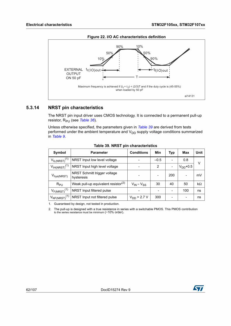
Electrical characteristics STM32F105xx, STM32F107xx
62/107 DocID15274 Rev 9
Figure 22. I/O AC characteristics definition
5.3.14 NRST pin characteristics
The NRST pin input driver uses CMOS technology. It is connected to a permanent pull-up resistor, RPU (see Table 36).
Unless otherwise specified, the parameters given in Table 39 are derived from tests performed under the ambient temperature and VDD supply voltage conditions summarized in Table 9.
ai14131
tr(IO)out
50%
90%
T
tf(IO)out
Maximum frequency is achieved if (t + t ) < (2/3)T and if the duty cycle is (45-55%)when loaded by 50 pF
r f
EXTERNALOUTPUTON 50 pF
10%
50%
90%
10%
Table 39. NRST pin characteristics
Symbol Parameter Conditions Min Typ Max Unit
VIL(NRST)(1)
1. Guaranteed by design, not tested in production.
NRST Input low level voltage - –0.5 - 0.8V
VIH(NRST)(1) NRST Input high level voltage - 2 - VDD+0.5
Vhys(NRST)NRST Schmitt trigger voltage hysteresis
- - 200 - mV
RPU Weak pull-up equivalent resistor(2)
2. The pull-up is designed with a true resistance in series with a switchable PMOS. This PMOS contribution to the series resistance must be minimum (~10% order).
VIN = VSS 30 40 50 kΩ
VF(NRST)(1) NRST Input filtered pulse - - - 100 ns
VNF(NRST)(1) NRST Input not filtered pulse VDD > 2.7 V 300 - - ns

DocID15274 Rev 9 63/107
STM32F105xx, STM32F107xx Electrical characteristics
106
Figure 23. Recommended NRST pin protection
2. The reset network protects the device against parasitic resets.
3. The user must ensure that the level on the NRST pin can go below the VIL(NRST) max level specified in Table 39. Otherwise the reset will not be taken into account by the device.
5.3.15 TIM timer characteristics
The parameters given in Table 40 are guaranteed by design.
Refer to Section 5.3.12: I/O current injection characteristics for details on the input/output alternate function characteristics (output compare, input capture, external clock, PWM output).
ai14132d
STM32F10xxx
RPUNRST(2)
VDD
Filter
Internal Reset
0.1 µF
Externalreset circuit(1)
Table 40. TIMx(1) characteristics
1. TIMx is used as a general term to refer to the TIM1, TIM2, TIM3, TIM4 and TIM5 timers.
Symbol Parameter Conditions Min Max Unit
tres(TIM) Timer resolution time - 1 - tTIMxCLK
fTIMxCLK = 72 MHz 13.9 - ns
fEXTTimer external clock frequency on CH1 to CH4
- 0 fTIMxCLK/2 MHz
fTIMxCLK = 72 MHz 0 36 MHz
ResTIM Timer resolution - - 16 bit
tCOUNTER
16-bit counter clock period when internal clock is selected
- 1 65536 tTIMxCLK
fTIMxCLK = 72 MHz 0.0139 910 µs
tMAX_COUNT Maximum possible count - - 65536 × 65536 tTIMxCLK
fTIMxCLK = 72 MHz - 59.6 s

Electrical characteristics STM32F105xx, STM32F107xx
64/107 DocID15274 Rev 9
5.3.16 Communications interfaces
I2C interface characteristics
Unless otherwise specified, the parameters given in Table 41 are derived from tests performed under the ambient temperature, fPCLK1 frequency and VDD supply voltage conditions summarized in Table 9.
The STM32F105xx and STM32F107xx I2C interface meets the requirements of the standard I2C communication protocol with the following restrictions: the I/O pins SDA and SCL are mapped to are not “true” open-drain. When configured as open-drain, the PMOS connected between the I/O pin and VDD is disabled, but is still present.
The I2C characteristics are described in Table 41. Refer also to Section 5.3.12: I/O current injection characteristics for more details on the input/output alternate function characteristics (SDA and SCL).
Table 41. I2C characteristics
Symbol ParameterStandard mode I2C(1)
1. Guaranteed by design, not tested in production.
Fast mode I2C(1)(2)
2. fPCLK1 must be at least 2 MHz to achieve standard mode I2C frequencies. It must be at least 4 MHz to achieve the fast mode I2C frequencies and it must be a mulitple of 10 MHz in order to reach I2C fast mode maximum clock 400 kHz.
UnitMin Max Min Max
tw(SCLL) SCL clock low time 4.7 - 1.3 -µs
tw(SCLH) SCL clock high time 4.0 - 0.6 -
tsu(SDA) SDA setup time 250 - 100 -
ns
th(SDA) SDA data hold time 0(3)
3. The maximum hold time of the Start condition has only to be met if the interface does not stretch the low period of SCL signal.
- 0(4)
4. The device must internally provide a hold time of at least 300ns for the SDA signal in order to bridge the undefined region of the falling edge of SCL.
900(3)
tr(SDA)tr(SCL)
SDA and SCL rise time - 1000 20 + 0.1Cb 300
tf(SDA)tf(SCL)
SDA and SCL fall time - 300 - 300
th(STA) Start condition hold time 4.0 - 0.6 -
µstsu(STA)
Repeated Start condition setup time
4.7 - 0.6 -
tsu(STO) Stop condition setup time 4.0 - 0.6 - μs
tw(STO:STA)Stop to Start condition time (bus free)
4.7 - 1.3 - μs
CbCapacitive load for each bus line
- 400 - 400 pF

DocID15274 Rev 9 65/107
STM32F105xx, STM32F107xx Electrical characteristics
106
Figure 24. I2C bus AC waveforms and measurement circuit
1. Measurement points are done at CMOS levels: 0.3VDD and 0.7VDD.
Table 42. SCL frequency (fPCLK1= 36 MHz.,VDD = 3.3 V)(1)(2)
1. RP = External pull-up resistance, fSCL = I2C speed,
2. For speeds around 200 kHz, the tolerance on the achieved speed is of ±5%. For other speed ranges, the tolerance on the achieved speed ±2%. These variations depend on the accuracy of the external components used to design the application.
fSCL (kHz)I2C_CCR value
RP = 4.7 kΩ
400 0x801E
300 0x8028
200 0x803C
100 0x00B4
50 0x0168
20 0x0384
ai14133d
Start
SDA
100 Ω4.7kΩ
I²C bus
4.7kΩ
100 Ω
VDDVDD
STM32F10x
SDA
SCL
tf(SDA) tr(SDA)
SCL
th(STA)
tw(SCLH)
tw(SCLL)
tsu(SDA)
tr(SCL) tf(SCL)
th(SDA)
Start repeated
Starttsu(STA)
tsu(STO)
Stop tsu(STO:STA)

Electrical characteristics STM32F105xx, STM32F107xx
66/107 DocID15274 Rev 9
I2S - SPI interface characteristics
Unless otherwise specified, the parameters given in Table 43 for SPI or in Table 44 for I2S are derived from tests performed under the ambient temperature, fPCLKx frequency and VDD supply voltage conditions summarized in Table 9.
Refer to Section 5.3.12: I/O current injection characteristics for more details on the input/output alternate function characteristics (NSS, SCK, MOSI, MISO for SPI and WS, CK, SD for I2S).
Table 43. SPI characteristics
Symbol Parameter Conditions Min Max Unit
fSCK1/tc(SCK)
SPI clock frequencyMaster mode - 18
MHzSlave mode - 18
tr(SCK)tf(SCK)
SPI clock rise and fall time
Capacitive load: C = 30 pF - 8 ns
DuCy(SCK)SPI slave input clock duty cycle
Slave mode 30 70 %
tsu(NSS) NSS setup time Slave mode 4 tPCLK -
ns
th(NSS) NSS hold time Slave mode 2 tPCLK -
tw(SCKH)tw(SCKL)
SCK high and low timeMaster mode, fPCLK = 36 MHz, presc = 4
50 60
tsu(MI) Data input setup time
Master mode 4 -
tsu(SI) Slave mode 5 -
th(MI) Data input hold time
Master mode 5 -
th(SI) Slave mode 5 -
ta(SO)Data output access time
Slave mode, fPCLK = 20 MHz - 3*tPCLK
tv(SO) Data output valid time Slave mode (after enable edge) - 34
tv(MO) Data output valid time Master mode (after enable edge) - 8
th(SO)Data output hold time
Slave mode (after enable edge) 32 -
th(MO) Master mode (after enable edge) 10 -

DocID15274 Rev 9 67/107
STM32F105xx, STM32F107xx Electrical characteristics
106
Figure 25. SPI timing diagram - slave mode and CPHA = 0
Figure 26. SPI timing diagram - slave mode and CPHA = 1(1)
1. Measurement points are done at CMOS levels: 0.3VDD and 0.7VDD.

Electrical characteristics STM32F105xx, STM32F107xx
68/107 DocID15274 Rev 9
Figure 27. SPI timing diagram - master mode(1)
1. Measurement points are done at CMOS levels: 0.3VDD and 0.7VDD.

DocID15274 Rev 9 69/107
STM32F105xx, STM32F107xx Electrical characteristics
106
Table 44. I2S characteristics
Symbol Parameter Conditions Min Max Unit
fCK1/tc(CK)
I2S clock frequency
Master data: 16 bits, audio freq = 48 K
1.52 1.54MHz
Slave 0 6.5
tr(CK)tf(CK)
I2S clock rise and fall time capacitive load CL = 50 pF - 8
ns
tw(CKH)(1) I2S clock high time Master fPCLK = 16 MHz,
audio freq = 48 K
317 320
tw(CKL)(1) I2S clock low time 333 336
tv(WS) (1) WS valid time Master mode 3 -
th(WS) (1) WS hold time Master mode
I2S2 0 -
I2S3 0 -
tsu(WS) (1) WS setup time Slave mode
I2S2 4 -
I2S3 9 -
th(WS) (1) WS hold time Slave mode 0 -
DuCy(SCK)I2S slave input clock duty cycle
Slave mode 30 70 %
tsu(SD_MR) (1)
Data input setup time
Master receiverI2S2 8 -
ns
I2S3 10 -
tsu(SD_SR) (1) Slave receiver
I2S2 3 -
I2S3 8 -
th(SD_MR)(1)
Data input hold time
Master receiverI2S2 2 -
I2S3 4 -
th(SD_SR) (1) Slave receiver
I2S2 2 -
I2S3 4 -
tv(SD_ST) (1)(3) Data output valid time
Slave transmitter (after enable edge)
I2S2 23 -
I2S3 33 -
th(SD_ST) (1) Data output hold time
Slave transmitter (after enable edge)
I2S2 29 -
I2S3 27 -
tv(SD_MT) (1) Data output valid time
Master transmitter (after enable edge)
I2S2 - 5
I2S3 - 2
th(SD_MT) (1) Data output hold time
Master transmitter (after enable edge)
I2S2 11 -
I2S3 4 -
1. Based on design simulation and/or characterization results, not tested in production.

Electrical characteristics STM32F105xx, STM32F107xx
70/107 DocID15274 Rev 9
Figure 28. I2S slave timing diagram (Philips protocol)(1)
1. Measurement points are done at CMOS levels: 0.3 × VDD and 0.7 × VDD.
2. LSB transmit/receive of the previously transmitted byte. No LSB transmit/receive is sent before the first byte.
Figure 29. I2S master timing diagram (Philips protocol)(1)
1. Based on characterization, not tested in production.
2. LSB transmit/receive of the previously transmitted byte. No LSB transmit/receive is sent before the first byte.

DocID15274 Rev 9 71/107
STM32F105xx, STM32F107xx Electrical characteristics
106
USB OTG FS characteristics
The USB OTG interface is USB-IF certified (Full-Speed).
Figure 30. USB OTG FS timings: definition of data signal rise and fall time
Table 45. USB OTG FS startup time
Symbol Parameter Max Unit
tSTARTUP(1)
1. Guaranteed by design, not tested in production.
USB OTG FS transceiver startup time 1 µs
Table 46. USB OTG FS DC electrical characteristics
Symbol Parameter Conditions Min.(1)
1. All the voltages are measured from the local ground potential.
Typ. Max.(1) Unit
Input levels
VDDUSB OTG FS operating voltage
- 3.0(2)
2. The STM32F105xx and STM32F107xx USB OTG FS functionality is ensured down to 2.7 V but not the full USB OTG FS electrical characteristics which are degraded in the 2.7-to-3.0 V VDD voltage range.
- 3.6 V
VDI(3)
3. Guaranteed by design, not tested in production.
Differential input sensitivity I(USBDP, USBDM) 0.2 - -
VVCM
(3) Differential common mode range
Includes VDI range 0.8 - 2.5
VSE(3) Single ended receiver
threshold - 1.3 - 2.0
Output levels
VOL Static output level low RL of 1.5 kΩ to 3.6 V(4)
4. RL is the load connected on the USB OTG FS drivers
- 0.3V
VOH Static output level high RL of 15 kΩ to VSS(4) 2.8 - 3.6
RPD
Pull-down resistance on PA11, PA12
VIN = VDD
17 21 24
kΩPull-down resistance on PA9
0.65 1.1 2.0
RPU
Pull-up resistance on PA12 VIN = VSS 1.5 1.8 2.1
Pull-up resistance on PA9 VIN = VSS 0.25 0.37 0.55
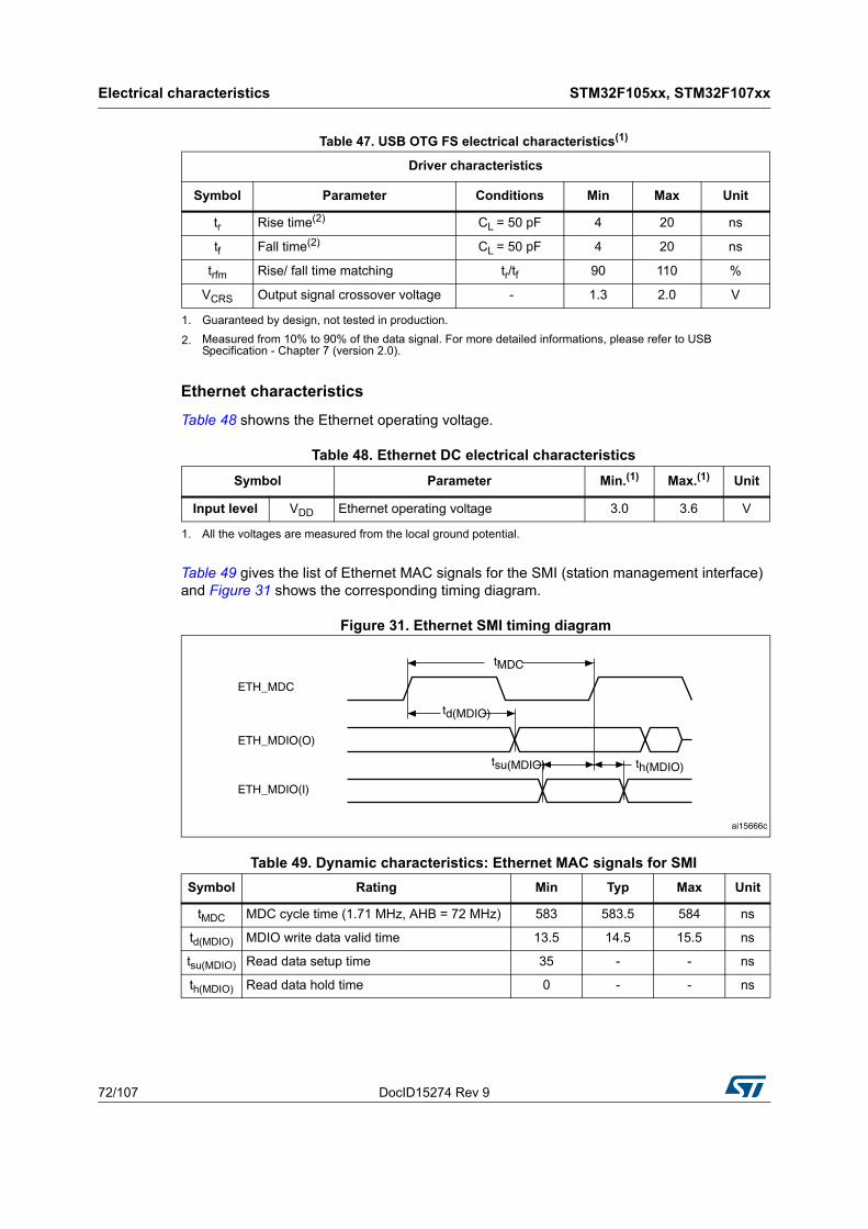
Electrical characteristics STM32F105xx, STM32F107xx
72/107 DocID15274 Rev 9
Ethernet characteristics
Table 48 showns the Ethernet operating voltage.
Table 49 gives the list of Ethernet MAC signals for the SMI (station management interface) and Figure 31 shows the corresponding timing diagram.
Figure 31. Ethernet SMI timing diagram
Table 47. USB OTG FS electrical characteristics(1)
1. Guaranteed by design, not tested in production.
Driver characteristics
Symbol Parameter Conditions Min Max Unit
tr Rise time(2)
2. Measured from 10% to 90% of the data signal. For more detailed informations, please refer to USB Specification - Chapter 7 (version 2.0).
CL = 50 pF 4 20 ns
tf Fall time(2) CL = 50 pF 4 20 ns
trfm Rise/ fall time matching tr/tf 90 110 %
VCRS Output signal crossover voltage - 1.3 2.0 V
Table 48. Ethernet DC electrical characteristics
Symbol Parameter Min.(1)
1. All the voltages are measured from the local ground potential.
Max.(1) Unit
Input level VDD Ethernet operating voltage 3.0 3.6 V
Table 49. Dynamic characteristics: Ethernet MAC signals for SMI
Symbol Rating Min Typ Max Unit
tMDC MDC cycle time (1.71 MHz, AHB = 72 MHz) 583 583.5 584 ns
td(MDIO) MDIO write data valid time 13.5 14.5 15.5 ns
tsu(MDIO) Read data setup time 35 - - ns
th(MDIO) Read data hold time 0 - - ns

DocID15274 Rev 9 73/107
STM32F105xx, STM32F107xx Electrical characteristics
106
Table 50 gives the list of Ethernet MAC signals for the RMII and Figure 32 shows the corresponding timing diagram.
Figure 32. Ethernet RMII timing diagram
Table 51 gives the list of Ethernet MAC signals for MII and Figure 32 shows the corresponding timing diagram.
Figure 33. Ethernet MII timing diagram
Table 50. Dynamic characteristics: Ethernet MAC signals for RMII
Symbol Rating Min Typ Max Unit
tsu(RXD) Receive data setup time 4 - - ns
tih(RXD) Receive data hold time 2 - - ns
tsu(DV) Carrier sense set-up time 4 - - ns
tih(DV) Carrier sense hold time 2 - - ns
td(TXEN) Transmit enable valid delay time 8 10 16 ns
td(TXD) Transmit data valid delay time 7 10 16 ns
MII_RX_CLK
MII_RXD[3:0]MII_RX_DVMII_RX_ER
td(TXEN)td(TXD)
tsu(RXD)tsu(ER)tsu(DV)
tih(RXD)tih(ER)tih(DV)
ai15668
MII_TX_CLK
MII_TX_ENMII_TXD[3:0]

Electrical characteristics STM32F105xx, STM32F107xx
74/107 DocID15274 Rev 9
CAN (controller area network) interface
Refer to Section 5.3.12: I/O current injection characteristics for more details on the input/output alternate function characteristics (CANTX and CANRX).
5.3.17 12-bit ADC characteristics
Unless otherwise specified, the parameters given in Table 52 are derived from tests performed under the ambient temperature, fPCLK2 frequency and VDDA supply voltage conditions summarized in Table 9.
Note: It is recommended to perform a calibration after each power-up.
Table 51. Dynamic characteristics: Ethernet MAC signals for MII
Symbol Rating Min Typ Max Unit
tsu(RXD) Receive data setup time 10 - - ns
tih(RXD) Receive data hold time 10 - - ns
tsu(DV) Data valid setup time 10 - - ns
tih(DV) Data valid hold time 10 - - ns
tsu(ER) Error setup time 10 - - ns
tih(ER) Error hold time 10 - - ns
td(TXEN) Transmit enable valid delay time 14 16 18 ns
td(TXD) Transmit data valid delay time 13 16 20 ns
Table 52. ADC characteristics
Symbol Parameter Conditions Min Typ Max Unit
VDDA Power supply - 2.4 - 3.6 V
VREF+ Positive reference voltage - 2.4 - VDDA V
IVREF Current on the VREF input pin - - 160(1) 220(1) µA
fADC ADC clock frequency - 0.6 - 14 MHz
fS(2) Sampling rate - 0.05 - 1 MHz
fTRIG(2) External trigger frequency
fADC = 14 MHz - - 823 kHz
- - - 17 1/fADC
VAIN Conversion voltage range(3) - 0 (VSSA or VREF- tied to ground)
- VREF+ V
RAIN(2) External input impedance
See Equation 1 and Table 53 for details
- - 50 kΩ
RADC(2) Sampling switch resistance - - - 1 kΩ
CADC(2) Internal sample and hold capacitor - - - 8 pF
tCAL(2) Calibration time
fADC = 14 MHz 5.9 µs
- 83 1/fADC
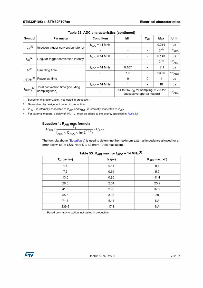
DocID15274 Rev 9 75/107
STM32F105xx, STM32F107xx Electrical characteristics
106
Equation 1: RAIN max formula
The formula above (Equation 1) is used to determine the maximum external impedance allowed for anerror below 1/4 of LSB. Here N = 12 (from 12-bit resolution).
tlat(2) Injection trigger conversion latency
fADC = 14 MHz - - 0.214 µs
- - - 3(4) 1/fADC
tlatr(2) Regular trigger conversion latency
fADC = 14 MHz - - 0.143 µs
- - - 2(4) 1/fADC
tS(2) Sampling time
fADC = 14 MHz 0.107 - 17.1 µs
- 1.5 - 239.5 1/fADC
tSTAB(2) Power-up time - 0 0 1 µs
tCONV(2) Total conversion time (including
sampling time)
fADC = 14 MHz 1 - 18 µs
-14 to 252 (tS for sampling +12.5 for
successive approximation)1/fADC
1. Based on characterization, not tested in production.
2. Guaranteed by design, not tested in production.
3. VREF+ is internally connected to VDDA and VREF- is internally connected to VSSA.
4. For external triggers, a delay of 1/fPCLK2 must be added to the latency specified in Table 52.
Table 52. ADC characteristics (continued)
Symbol Parameter Conditions Min Typ Max Unit
Table 53. RAIN max for fADC = 14 MHz(1)
1. Based on characterization, not tested in production.
Ts (cycles) tS (µs) RAIN max (kΩ)
1.5 0.11 0.4
7.5 0.54 5.9
13.5 0.96 11.4
28.5 2.04 25.2
41.5 2.96 37.2
55.5 3.96 50
71.5 5.11 NA
239.5 17.1 NA
RAIN
TS
fADC CADC 2N 2+( )ln××
---------------------------------------------------------------- RADC–<
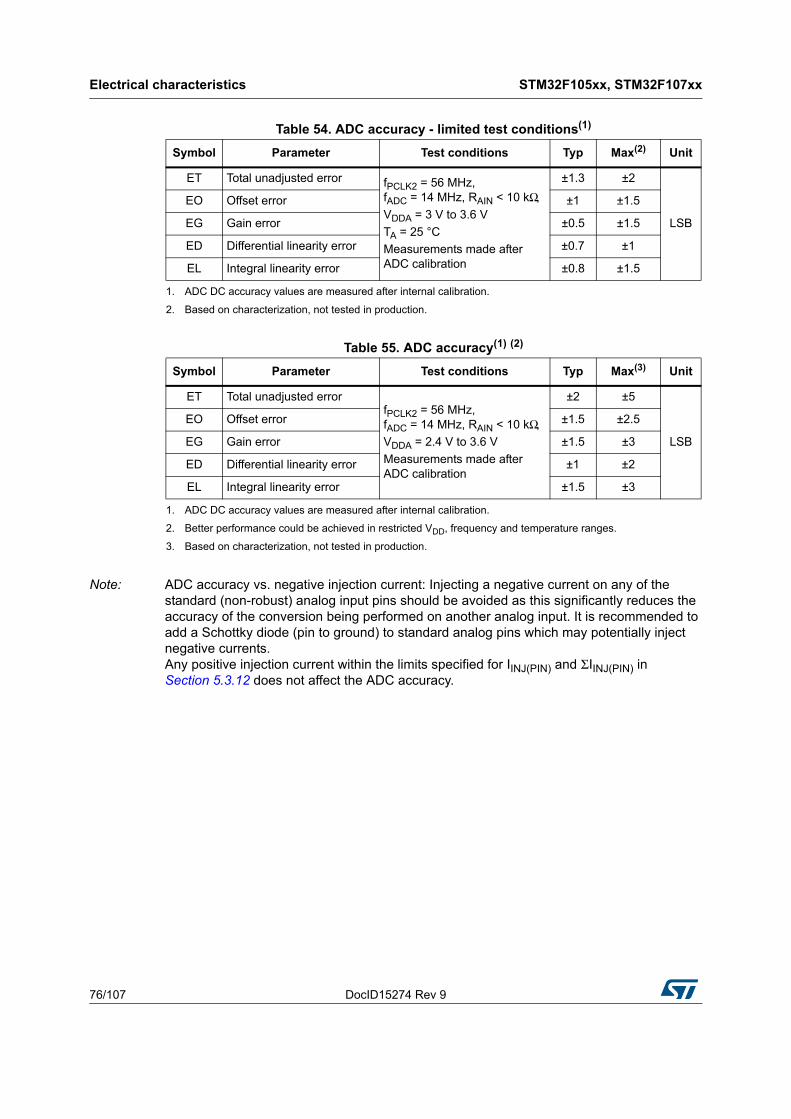
Electrical characteristics STM32F105xx, STM32F107xx
76/107 DocID15274 Rev 9
Note: ADC accuracy vs. negative injection current: Injecting a negative current on any of the standard (non-robust) analog input pins should be avoided as this significantly reduces the accuracy of the conversion being performed on another analog input. It is recommended to add a Schottky diode (pin to ground) to standard analog pins which may potentially inject negative currents.Any positive injection current within the limits specified for IINJ(PIN) and ΣIINJ(PIN) in Section 5.3.12 does not affect the ADC accuracy.
Table 54. ADC accuracy - limited test conditions(1)
1. ADC DC accuracy values are measured after internal calibration.
Symbol Parameter Test conditions Typ Max(2)
2. Based on characterization, not tested in production.
Unit
ET Total unadjusted error fPCLK2 = 56 MHz,fADC = 14 MHz, RAIN < 10 kΩ,
VDDA = 3 V to 3.6 V
TA = 25 °C
Measurements made after ADC calibration
±1.3 ±2
LSB
EO Offset error ±1 ±1.5
EG Gain error ±0.5 ±1.5
ED Differential linearity error ±0.7 ±1
EL Integral linearity error ±0.8 ±1.5
Table 55. ADC accuracy(1) (2)
1. ADC DC accuracy values are measured after internal calibration.
2. Better performance could be achieved in restricted VDD, frequency and temperature ranges.
Symbol Parameter Test conditions Typ Max(3)
3. Based on characterization, not tested in production.
Unit
ET Total unadjusted errorfPCLK2 = 56 MHz,fADC = 14 MHz, RAIN < 10 kΩ,
VDDA = 2.4 V to 3.6 V
Measurements made after ADC calibration
±2 ±5
LSB
EO Offset error ±1.5 ±2.5
EG Gain error ±1.5 ±3
ED Differential linearity error ±1 ±2
EL Integral linearity error ±1.5 ±3

DocID15274 Rev 9 77/107
STM32F105xx, STM32F107xx Electrical characteristics
106
Figure 34. ADC accuracy characteristics
Figure 35. Typical connection diagram using the ADC
1. Refer to Table 52 for the values of RAIN, RADC and CADC.
2. Cparasitic represents the capacitance of the PCB (dependent on soldering and PCB layout quality) plus the pad capacitance (roughly 7 pF). A high Cparasitic value will downgrade conversion accuracy. To remedy this, fADC should be reduced.

Electrical characteristics STM32F105xx, STM32F107xx
78/107 DocID15274 Rev 9
General PCB design guidelines
Power supply decoupling should be performed as shown in Figure 36 or Figure 37, depending on whether VREF+ is connected to VDDA or not. The 10 nF capacitors should be ceramic (good quality). They should be placed them as close as possible to the chip.
Figure 36. Power supply and reference decoupling (VREF+ not connected to VDDA)
1. VREF+ and VREF– inputs are available only on 100-pin packages.
Figure 37. Power supply and reference decoupling (VREF+ connected to VDDA)
1. VREF+ and VREF– inputs are available only on 100-pin packages.
VREF+
STM32F10xxx
VDDA
VSSA/V REF-
1 µF // 10 nF
1 µF // 10 nF
ai14380c
(See note 1)
(See note 1)
VREF+/VDDA
STM32F10xxx
1 µF // 10 nF
VREF–/VSSA
ai14381c
(See note 1)
(See note 1)
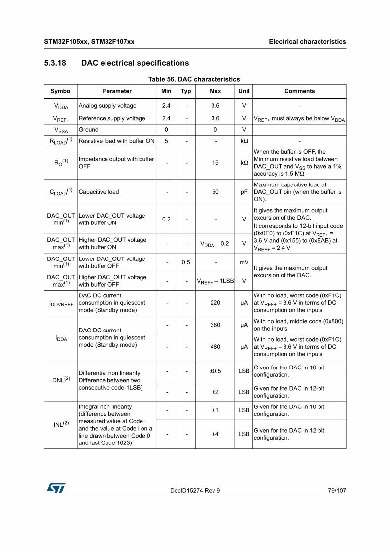
DocID15274 Rev 9 79/107
STM32F105xx, STM32F107xx Electrical characteristics
106
5.3.18 DAC electrical specifications
Table 56. DAC characteristics
Symbol Parameter Min Typ Max Unit Comments
VDDA Analog supply voltage 2.4 - 3.6 V -
VREF+ Reference supply voltage 2.4 - 3.6 V VREF+ must always be below VDDA
VSSA Ground 0 - 0 V -
RLOAD(1) Resistive load with buffer ON 5 - - kΩ -
RO(1) Impedance output with buffer
OFF - - 15 kΩ
When the buffer is OFF, the Minimum resistive load between DAC_OUT and VSS to have a 1% accuracy is 1.5 MΩ
CLOAD(1) Capacitive load - - 50 pF
Maximum capacitive load at DAC_OUT pin (when the buffer is ON).
DAC_OUT min(1)
Lower DAC_OUT voltage with buffer ON
0.2 - - V
It gives the maximum output excursion of the DAC.
It corresponds to 12-bit input code (0x0E0) to (0xF1C) at VREF+ = 3.6 V and (0x155) to (0xEAB) at VREF+ = 2.4 V
DAC_OUT max(1)
Higher DAC_OUT voltage with buffer ON
- - VDDA – 0.2 V
DAC_OUT min(1)
Lower DAC_OUT voltage with buffer OFF
- 0.5 - mVIt gives the maximum output excursion of the DAC.DAC_OUT
max(1)Higher DAC_OUT voltage with buffer OFF
- - VREF+ – 1LSB V
IDDVREF+
DAC DC current consumption in quiescent mode (Standby mode)
- - 220 µAWith no load, worst code (0xF1C) at VREF+ = 3.6 V in terms of DC consumption on the inputs
IDDA
DAC DC current consumption in quiescent mode (Standby mode)
- - 380 µAWith no load, middle code (0x800) on the inputs
- - 480 µAWith no load, worst code (0xF1C) at VREF+ = 3.6 V in terms of DC consumption on the inputs
DNL(2)Differential non linearity Difference between two consecutive code-1LSB)
- - ±0.5 LSBGiven for the DAC in 10-bit configuration.
- - ±2 LSBGiven for the DAC in 12-bit configuration.
INL(2)
Integral non linearity (difference between measured value at Code i and the value at Code i on a line drawn between Code 0 and last Code 1023)
- - ±1 LSBGiven for the DAC in 10-bit configuration.
- - ±4 LSBGiven for the DAC in 12-bit configuration.

Electrical characteristics STM32F105xx, STM32F107xx
80/107 DocID15274 Rev 9
Figure 38. 12-bit buffered /non-buffered DAC
1. The DAC integrates an output buffer that can be used to reduce the output impedance and to drive external loads directly without the use of an external operational amplifier. The buffer can be bypassed by configuring the BOFFx bit in the DAC_CR register.
Offset(2)
Offset error
(difference between measured value at Code (0x800) and the ideal value = VREF+/2)
- - ±10 mVGiven for the DAC in 12-bit configuration
- - ±3 LSBGiven for the DAC in 10-bit at VREF+ = 3.6 V
- - ±12 LSBGiven for the DAC in 12-bit at VREF+ = 3.6 V
Gain error(2) Gain error - - ±0.5 %
Given for the DAC in 12bit configuration
tSETTLING(2)
Settling time (full scale: for a 10-bit input code transition between the lowest and the highest input codes when DAC_OUT reaches final value ±1LSB
- 3 4 µsCLOAD ≤ 50 pF,RLOAD ≥ 5 kΩ
Update rate(2)
Max frequency for a correct DAC_OUT change when small variation in the input code (from code i to i+1LSB)
- - 1 MS/sCLOAD ≤ 50 pF,RLOAD ≥ 5 kΩ
tWAKEUP(2)
Wakeup time from off state (Setting the ENx bit in the DAC Control register)
- 6.5 10 µsCLOAD ≤ 50 pF, RLOAD ≥ 5 kΩinput code between lowest and highest possible ones.
PSRR+ (1)Power supply rejection ratio (to VDDA) (static DC measurement
- –67 –40 dB No RLOAD, CLOAD = 50 pF
1. Guaranteed by design, not tested in production.
2. Guaranteed by characterization, not tested in production.
Table 56. DAC characteristics (continued)
Symbol Parameter Min Typ Max Unit Comments
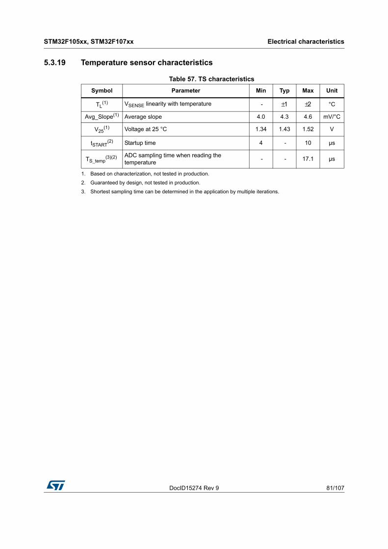
DocID15274 Rev 9 81/107
STM32F105xx, STM32F107xx Electrical characteristics
106
5.3.19 Temperature sensor characteristics
Table 57. TS characteristics
Symbol Parameter Min Typ Max Unit
TL(1)
1. Based on characterization, not tested in production.
VSENSE linearity with temperature - ±1 ±2 °C
Avg_Slope(1) Average slope 4.0 4.3 4.6 mV/°C
V25(1) Voltage at 25 °C 1.34 1.43 1.52 V
tSTART(2)
2. Guaranteed by design, not tested in production.
Startup time 4 - 10 µs
TS_temp(3)(2)
3. Shortest sampling time can be determined in the application by multiple iterations.
ADC sampling time when reading the temperature
- - 17.1 µs

Package characteristics STM32F105xx, STM32F107xx
82/107 DocID15274 Rev 9
6 Package characteristics
6.1 Package mechanical data
In order to meet environmental requirements, ST offers these devices in different grades of ECOPACK® packages, depending on their level of environmental compliance. ECOPACK® specifications, grade definitions and product status are available at: www.st.com. ECOPACK® is an ST trademark.
Figure 39. LFBGA100 - 10 x 10 mm low profile fine pitch ball grid array packageoutline

DocID15274 Rev 9 83/107
STM32F105xx, STM32F107xx Package characteristics
106
Figure 41. LFBGA100 – 100-ball low profile fine pitch ball grid array, 10 x 10 mm,0.8 mm pitch, package recommended footprint
Figure 40. LFBGA100 – 100-ball low profile fine pitch ball grid array, 10 x 10 mm,0.8 mm pitch, package mechanical data
Symbolmillimeters inches(1)
1. Values in inches are converted from mm and rounded to 4 decimal digits.
Min Typ Max Typ Min Max
A - - 1.700 - - 0.0669
A1 0.270 - - 0.0106 - -
A2 - 0.300 - - 0.0118 -
A4 - - 0.800 - - 0.0315
b 0.450 0.500 0.550 0.0177 0.0197 0.0217
D 9.850 10.000 10.150 0.3878 0.3937 0.3996
D1 - 7.200 - - 0.2835 -
E 9.850 10.000 10.150 0.3878 0.3937 0.3996
E1 - 7.200 - - 0.2835 -
e - 0.800 - - 0.0315 -
F - 1.400 - - 0.0551 -
ddd - - 0.120 - - 0.0047
eee - - 0.150 - - 0.0059
fff - - 0.080 - - 0.0031
Table 58. LFBGA100 recommended PCB design rules (0.8 mm pitch BGA)
Dimension Recommended values
Pitch 0.8
Dpad 0.500 mm
Dsm0.570 mm typ. (depends on the soldermask registration tolerance)
Stencil opening 0.500 mm
Stencil thickness Between 0.100 mm and 0.125 mm
Pad trace width 0.120 mm
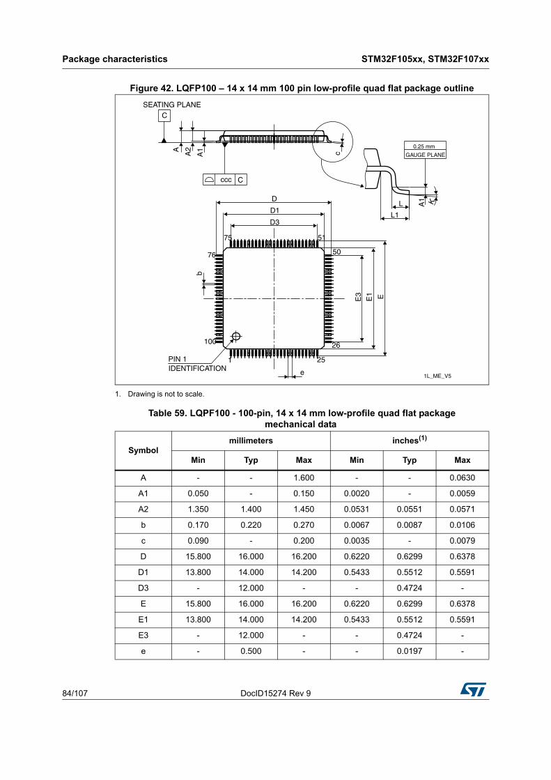
Package characteristics STM32F105xx, STM32F107xx
84/107 DocID15274 Rev 9
Figure 42. LQFP100 – 14 x 14 mm 100 pin low-profile quad flat package outline
1. Drawing is not to scale.
Table 59. LQPF100 - 100-pin, 14 x 14 mm low-profile quad flat package mechanical data
Symbolmillimeters inches(1)
Min Typ Max Min Typ Max
A - - 1.600 - - 0.0630
A1 0.050 - 0.150 0.0020 - 0.0059
A2 1.350 1.400 1.450 0.0531 0.0551 0.0571
b 0.170 0.220 0.270 0.0067 0.0087 0.0106
c 0.090 - 0.200 0.0035 - 0.0079
D 15.800 16.000 16.200 0.6220 0.6299 0.6378
D1 13.800 14.000 14.200 0.5433 0.5512 0.5591
D3 - 12.000 - - 0.4724 -
E 15.800 16.000 16.200 0.6220 0.6299 0.6378
E1 13.800 14.000 14.200 0.5433 0.5512 0.5591
E3 - 12.000 - - 0.4724 -
e - 0.500 - - 0.0197 -

DocID15274 Rev 9 85/107
STM32F105xx, STM32F107xx Package characteristics
106
Figure 43. LQFP100 - 100-pin, 14 x 14 mm low-profile quad flat recommended footprint
L 0.450 0.600 0.750 0.0177 0.0236 0.0295
L1 - 1.000 - - 0.0394 -
k 0.0° 3.5° 7.0° 0.0° 3.5° 7.0°
ccc - - 0.080 - - 0.0031
1. Values in inches are converted from mm and rounded to 4 decimal digits.
Table 59. LQPF100 - 100-pin, 14 x 14 mm low-profile quad flat package mechanical data (continued)
Symbolmillimeters inches(1)
Min Typ Max Min Typ Max
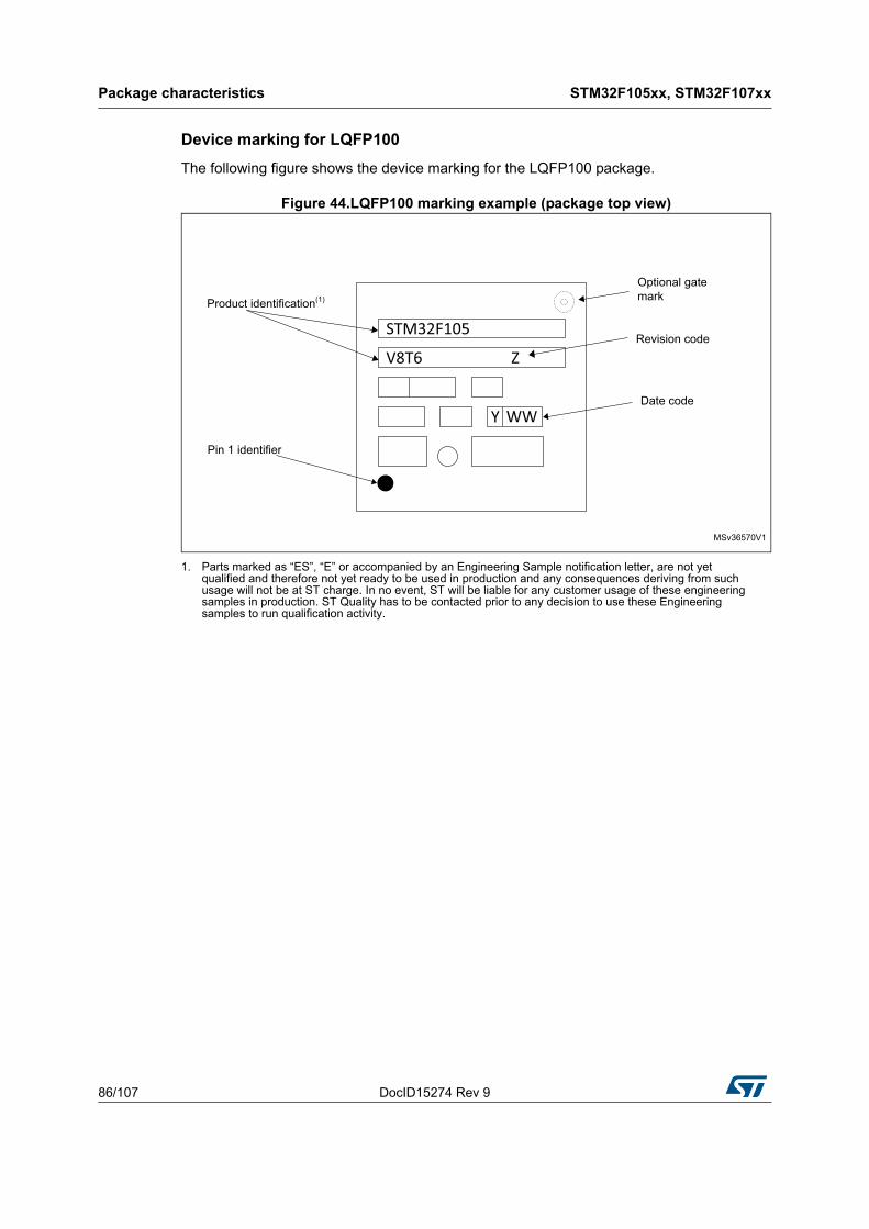
Package characteristics STM32F105xx, STM32F107xx
86/107 DocID15274 Rev 9
Device marking for LQFP100
The following figure shows the device marking for the LQFP100 package.
Figure 44.LQFP100 marking example (package top view)
1. Parts marked as “ES”, “E” or accompanied by an Engineering Sample notification letter, are not yet qualified and therefore not yet ready to be used in production and any consequences deriving from such usage will not be at ST charge. In no event, ST will be liable for any customer usage of these engineering samples in production. ST Quality has to be contacted prior to any decision to use these Engineering samples to run qualification activity.

DocID15274 Rev 9 87/107
STM32F105xx, STM32F107xx Package characteristics
106
Figure 45.LQFP64 – 10 x 10 mm 64 pin low-profile quad flat package outline
1. Drawing is not in scale.
Table 60.LQFP64 – 10 x 10 mm 64 pin low-profile quad flat package mechanical data
Symbolmillimeters inches(1)
Min Typ Max Min Typ Max
A - - 1.600 - - 0.0630
A1 0.050 - 0.150 0.0020 - 0.0059
A2 1.350 1.400 1.450 0.0531 0.0551 0.0571
b 0.170 0.220 0.270 0.0067 0.0087 0.0106
c 0.090 - 0.200 0.0035 - 0.0079
D - 12.000 - - 0.4724 -
D1 - 10.000 - - 0.3937 -
D3 - 7.500 - - 0.2953 -
E - 12.000 - - 0.4724 -
E1 - 10.000 - - 0.3937 -
E3 - 7.500 - - 0.2953 -
e - 0.500 - - 0.0197 -
θ 0° 3.5° 7° 0° 3.5° 7°

Package characteristics STM32F105xx, STM32F107xx
88/107 DocID15274 Rev 9
Figure 46.LQFP64 - 64-pin, 10 x 10 mm low-profile quad flat recommended footprint
1. Dimensions are in millimeters.
L 0.450 0.600 0.750 0.0177 0.0236 0.0295
L1 - 1.000 - - 0.0394 -
ccc - - 0.080 - - 0.0031
1. Values in inches are converted from mm and rounded to 4 decimal digits.
Table 60.LQFP64 – 10 x 10 mm 64 pin low-profile quad flat package mechanical data
Symbolmillimeters inches(1)
Min Typ Max Min Typ Max

DocID15274 Rev 9 89/107
STM32F105xx, STM32F107xx Package characteristics
106
Device marking for LQFP64
The following figure shows the device marking for the LQFP64 package.
Figure 47.LQFP64 marking example (package top view)
1. Parts marked as “ES”, “E” or accompanied by an Engineering Sample notification letter, are not yet qualified and therefore not yet ready to be used in production and any consequences deriving from such usage will not be at ST charge. In no event, ST will be liable for any customer usage of these engineering samples in production. ST Quality has to be contacted prior to any decision to use these Engineering samples to run qualification activity.
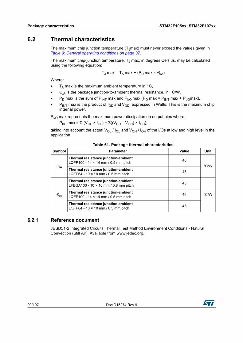
Package characteristics STM32F105xx, STM32F107xx
90/107 DocID15274 Rev 9
6.2 Thermal characteristics
The maximum chip junction temperature (TJmax) must never exceed the values given in Table 9: General operating conditions on page 37.
The maximum chip-junction temperature, TJ max, in degrees Celsius, may be calculated using the following equation:
TJ max = TA max + (PD max × ΘJA)
Where:
• TA max is the maximum ambient temperature in ° C,
• ΘJA is the package junction-to-ambient thermal resistance, in ° C/W,
• PD max is the sum of PINT max and PI/O max (PD max = PINT max + PI/Omax),
• PINT max is the product of IDD and VDD, expressed in Watts. This is the maximum chip internal power.
PI/O max represents the maximum power dissipation on output pins where:
PI/O max = Σ (VOL × IOL) + Σ((VDD – VOH) × IOH),
taking into account the actual VOL / IOL and VOH / IOH of the I/Os at low and high level in the application.
6.2.1 Reference document
JESD51-2 Integrated Circuits Thermal Test Method Environment Conditions - Natural Convection (Still Air). Available from www.jedec.org.
Table 61. Package thermal characteristics
Symbol Parameter Value Unit
ΘJA
Thermal resistance junction-ambientLQFP100 - 14 × 14 mm / 0.5 mm pitch
46
°C/WThermal resistance junction-ambientLQFP64 - 10 × 10 mm / 0.5 mm pitch
45
ΘJA
Thermal resistance junction-ambientLFBGA100 - 10 × 10 mm / 0.8 mm pitch
40
°C/WThermal resistance junction-ambientLQFP100 - 14 × 14 mm / 0.5 mm pitch
46
Thermal resistance junction-ambientLQFP64 - 10 × 10 mm / 0.5 mm pitch
45

DocID15274 Rev 9 91/107
STM32F105xx, STM32F107xx Package characteristics
106
6.2.2 Selecting the product temperature range
When ordering the microcontroller, the temperature range is specified in the ordering information scheme shown in Table 62: Ordering information scheme.
Each temperature range suffix corresponds to a specific guaranteed ambient temperature at maximum dissipation and, to a specific maximum junction temperature.
As applications do not commonly use the STM32F103xx at maximum dissipation, it is useful to calculate the exact power consumption and junction temperature to determine which temperature range will be best suited to the application.
The following examples show how to calculate the temperature range needed for a given application.
Example 1: High-performance application
Assuming the following application conditions:
Maximum ambient temperature TAmax = 82 °C (measured according to JESD51-2), IDDmax = 50 mA, VDD = 3.5 V, maximum 20 I/Os used at the same time in output at low level with IOL = 8 mA, VOL= 0.4 V and maximum 8 I/Os used at the same time in output at low level with IOL = 20 mA, VOL= 1.3 V
PINTmax = 50 mA × 3.5 V= 175 mW
PIOmax = 20 × 8 mA × 0.4 V + 8 × 20 mA × 1.3 V = 272 mW
This gives: PINTmax = 175 mW and PIOmax = 272 mW:
PDmax = 175 + 272 = 447 mW
Thus: PDmax = 447 mW
Using the values obtained in Table 61 TJmax is calculated as follows:
– For LQFP100, 46 °C/W
TJmax = 82 °C + (46 °C/W × 447 mW) = 82 °C + 20.6 °C = 102.6 °C
This is within the range of the suffix 6 version parts (–40 < TJ < 105 °C).
In this case, parts must be ordered at least with the temperature range suffix 6 (see Table 62: Ordering information scheme).
Example 2: High-temperature application
Using the same rules, it is possible to address applications that run at high ambient temperatures with a low dissipation, as long as junction temperature TJ remains within the specified range.
Assuming the following application conditions:
Maximum ambient temperature TAmax = 115 °C (measured according to JESD51-2), IDDmax = 20 mA, VDD = 3.5 V, maximum 20 I/Os used at the same time in output at low level with IOL = 8 mA, VOL= 0.4 V
PINTmax = 20 mA × 3.5 V= 70 mW
PIOmax = 20 × 8 mA × 0.4 V = 64 mW
This gives: PINTmax = 70 mW and PIOmax = 64 mW:
PDmax = 70 + 64 = 134 mW
Thus: PDmax = 134 mW

Package characteristics STM32F105xx, STM32F107xx
92/107 DocID15274 Rev 9
Using the values obtained in Table 61 TJmax is calculated as follows:
– For LQFP100, 46 °C/W
TJmax = 115 °C + (46 °C/W × 134 mW) = 115 °C + 6.2 °C = 121.2 °C
This is within the range of the suffix 7 version parts (–40 < TJ < 125 °C).
In this case, parts must be ordered at least with the temperature range suffix 7 (see Table 62: Ordering information scheme).
Figure 48. LQFP100 PD max vs. TA
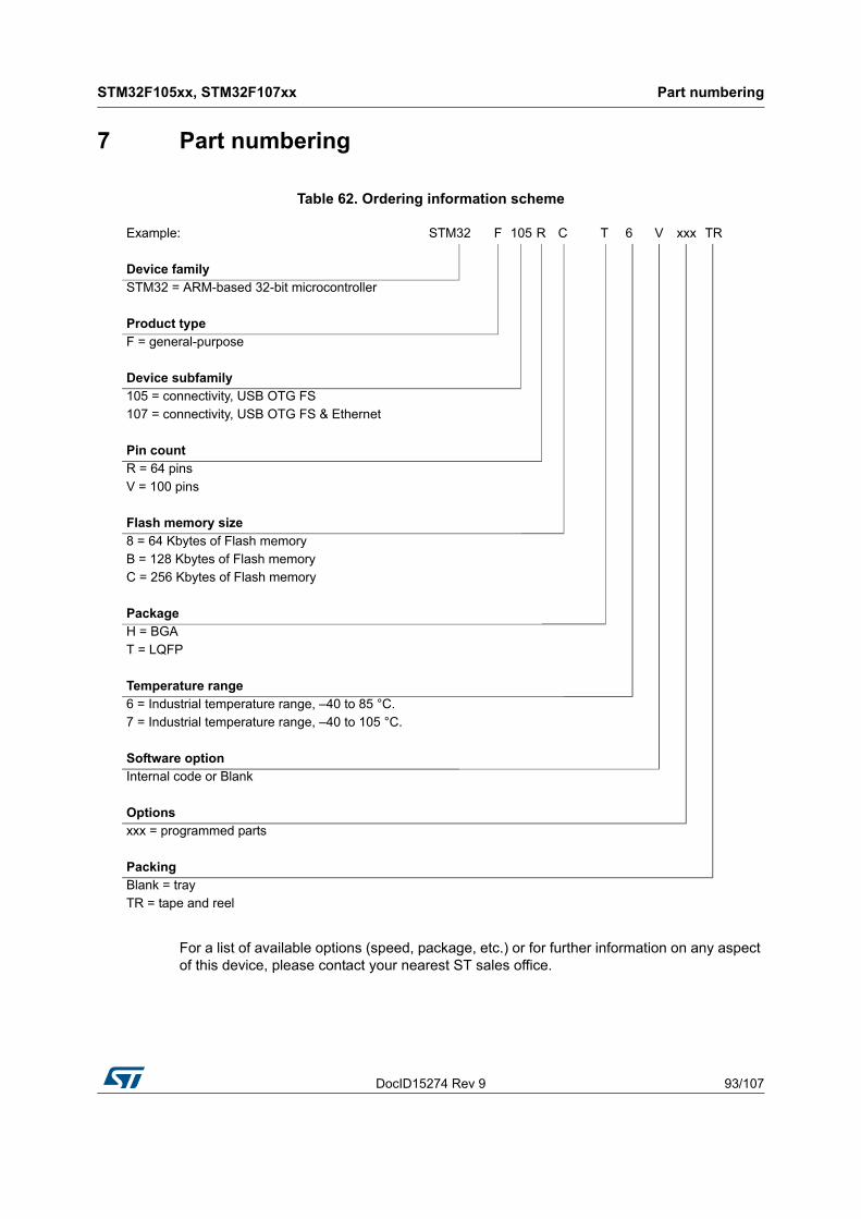
DocID15274 Rev 9 93/107
STM32F105xx, STM32F107xx Part numbering
106
7 Part numbering
For a list of available options (speed, package, etc.) or for further information on any aspect of this device, please contact your nearest ST sales office.
Table 62. Ordering information scheme
Example: STM32 F 105 R C T 6 V xxx TR
Device familySTM32 = ARM-based 32-bit microcontroller
Product typeF = general-purpose
Device subfamily105 = connectivity, USB OTG FS107 = connectivity, USB OTG FS & Ethernet
Pin countR = 64 pinsV = 100 pins
Flash memory size8 = 64 Kbytes of Flash memoryB = 128 Kbytes of Flash memoryC = 256 Kbytes of Flash memory
PackageH = BGAT = LQFP
Temperature range6 = Industrial temperature range, –40 to 85 °C.7 = Industrial temperature range, –40 to 105 °C.
Software optionInternal code or Blank
Optionsxxx = programmed parts
PackingBlank = trayTR = tape and reel
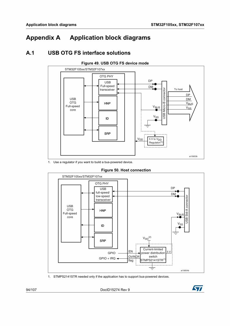
Application block diagrams STM32F105xx, STM32F107xx
94/107 DocID15274 Rev 9
Appendix A Application block diagrams
A.1 USB OTG FS interface solutions
Figure 49. USB OTG FS device mode
1. Use a regulator if you want to build a bus-powered device.
Figure 50. Host connection
1. STMPS2141STR needed only if the application has to support bus-powered devices.

DocID15274 Rev 9 95/107
STM32F105xx, STM32F107xx Application block diagrams
106
Figure 51. OTG connection (any protocol)
1. STMPS2141STR needed only if the application has to support bus-powered devices.
USBOTG
Full-speedcore
STM32F105xx/STM32F107xx
USBfull-speed/low-speedtransceiver
DP
US
B M
icro
-AB
con
nect
orDM
VBUS
VSS
HNPHNP
SRPSRP
IDID
OTG PHY
ai15655b
GPIO
GPIO + IRQ
ENCurrent-limited
power distributionswitch
STMPS2141STR(1)
ID
OVRCRflag
VDD
5 V

Application block diagrams STM32F105xx, STM32F107xx
96/107 DocID15274 Rev 9
A.2 Ethernet interface solutions
Figure 52. MII mode using a 25 MHz crystal
1. HCLK must be greater than 25 MHz.
2. Pulse per second when using IEEE1588 PTP, optional signal.
Figure 53. RMII with a 50 MHz oscillator
1. HCLK must be greater than 25 MHz.
MCUEthernetMAC 10/100
EthernetPHY 10/100
PLL HCLK
XT1PHY_CLK 25 MHz
MII_RX_CLKMII_RXD[3:0]MII_RX_DVMII_RX_ER
MII_TX_CLKMII_TX_ENMII_TXD[3:0]MII_CRSMII_COL
MDIOMDC
HCLK(1)
PPS_OUT(2)
XTAL25 MHz
STM32F107xx
OSC
TIM2 Timestampcomparator
Timer input trigger
IEEE1588 PTP
MII = 15 pins
MII + MDC = 17 pins
ai15656
MCUEthernetMAC 10/100
EthernetPHY 10/100
PLL HCLK
XT1PHY_CLK 50 MHz
RMII_RXD[1:0]
RMII_CRX_DV
RMII_REF_CLK
RMII_TX_EN
RMII_TXD[1:0]
MDIO
MDC
HCLK(1)
STM32F107xx
OSC50 MHz
TIM2 Timestampcomparator
Timer input trigger
IEEE1588 PTP
RMII= 7 pins
RMII + MDC = 9 pins
ai15657
/2 or /20synchronous2.5 or 25 MHz 50 MHz
50 MHz
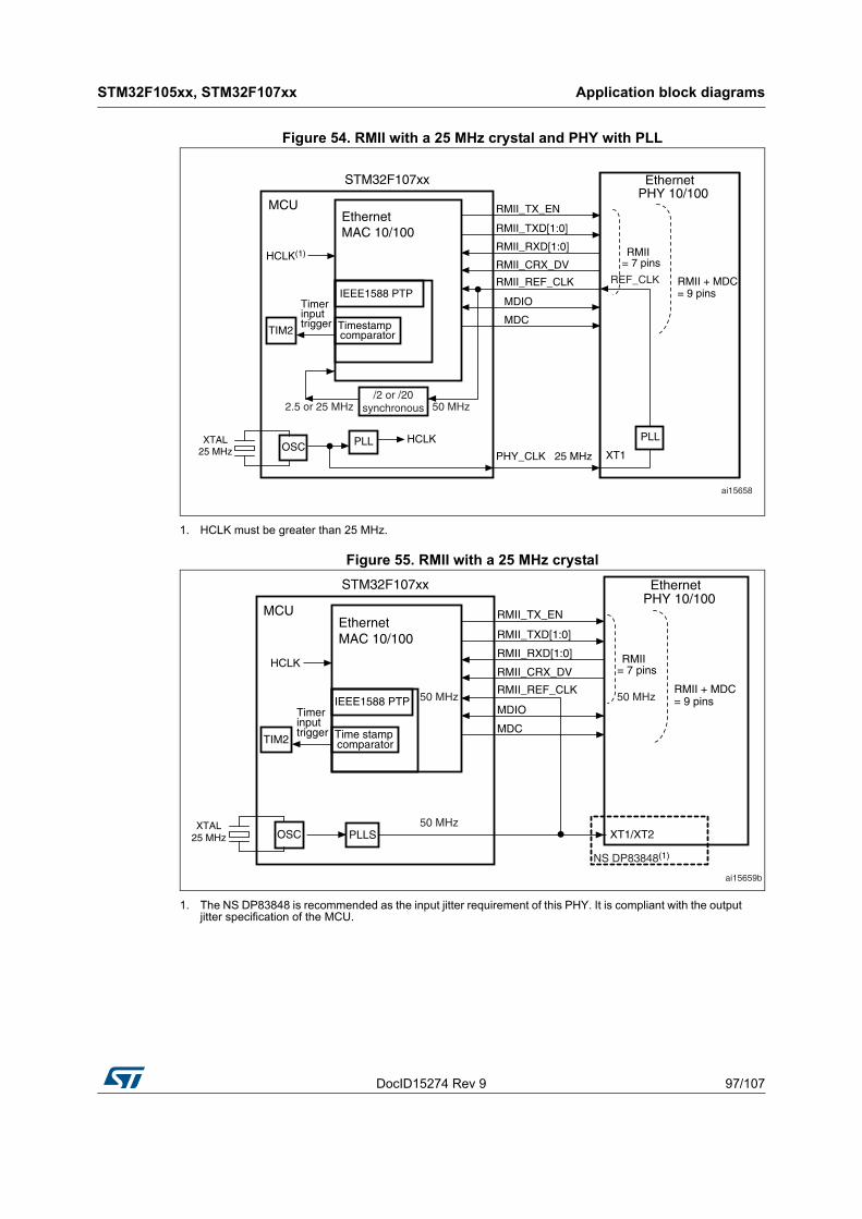
DocID15274 Rev 9 97/107
STM32F105xx, STM32F107xx Application block diagrams
106
Figure 54. RMII with a 25 MHz crystal and PHY with PLL
1. HCLK must be greater than 25 MHz.
Figure 55. RMII with a 25 MHz crystal
1. The NS DP83848 is recommended as the input jitter requirement of this PHY. It is compliant with the output jitter specification of the MCU.
MCUEthernetMAC 10/100
EthernetPHY 10/100
PLL HCLK
XT1PHY_CLK 25 MHz
RMII_RXD[1:0]
RMII_CRX_DV
RMII_REF_CLK
RMII_TX_EN
RMII_TXD[1:0]
MDIO
MDC
HCLK(1)
STM32F107xx
TIM2 Timestampcomparator
Timer input trigger
IEEE1588 PTP
RMII= 7 pins
RMII + MDC = 9 pins
ai15658
/2 or /20synchronous2.5 or 25 MHz 50 MHz
XTAL25 MHz OSC
PLL
REF_CLK
MCUEthernetMAC 10/100
EthernetPHY 10/100
PLLS XT1/XT2
RMII_RXD[1:0]
RMII_CRX_DV
RMII_REF_CLK
RMII_TX_EN
RMII_TXD[1:0]
MDIO
MDC
HCLK
STM32F107xx
TIM2 Time stampcomparator
Timer input trigger
IEEE1588 PTP
RMII= 7 pins
RMII + MDC = 9 pins
ai15659b
50 MHz
XTAL25 MHz OSC
NS DP83848(1)
50 MHz
50 MHz
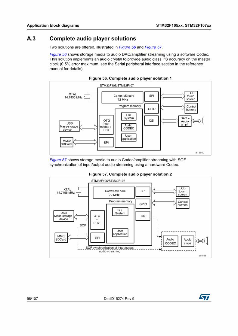
Application block diagrams STM32F105xx, STM32F107xx
98/107 DocID15274 Rev 9
A.3 Complete audio player solutions
Two solutions are offered, illustrated in Figure 56 and Figure 57.
Figure 56 shows storage media to audio DAC/amplifier streaming using a software Codec. This solution implements an audio crystal to provide audio class I2S accuracy on the master clock (0.5% error maximum, see the Serial peripheral interface section in the reference manual for details).
Figure 56. Complete audio player solution 1
Figure 57 shows storage media to audio Codec/amplifier streaming with SOF synchronization of input/output audio streaming using a hardware Codec.
Figure 57. Complete audio player solution 2
Cortex-M3 core72 MHz
OTG (host
mode) + PHY
SPI
SPI
GPIO
I2S
XTAL14.7456 MHz
USBMass-storage
device
MMC/SDCard
LCDtouchscreen
Controlbuttons
DAC + Audio ampli
File System
Program memory
Audio CODEC
User application
STM32F105/STM32F107
ai15660
Cortex-M3 core72 MHz
OTG+
PHY
SPI
SPI
GPIO
I2S
XTAL14.7456 MHz
USBMass-storage
device
MMC/SDCard
LCDtouchscreen
Controlbuttons
Audio ampli
File System
Program memory
Audio CODEC
User application
STM32F105/STM32F107
ai15661
SOF
SOF synchronization of input/outputaudio streaming
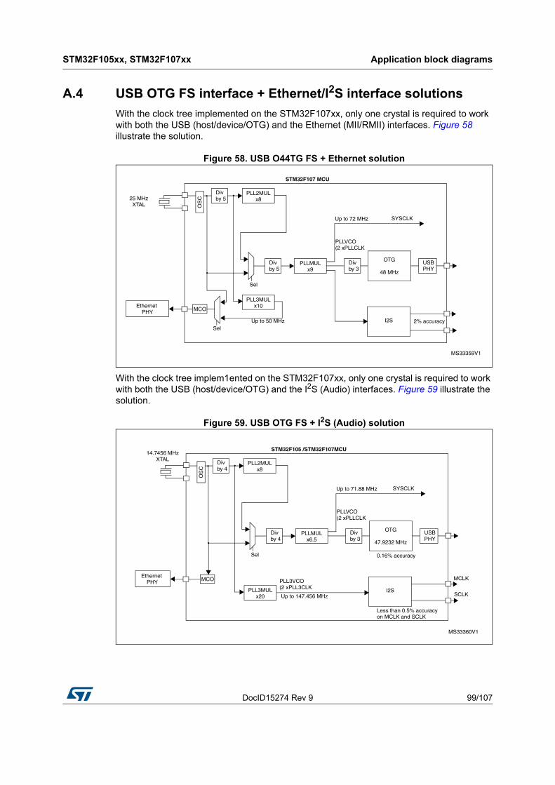
DocID15274 Rev 9 99/107
STM32F105xx, STM32F107xx Application block diagrams
106
A.4 USB OTG FS interface + Ethernet/I2S interface solutions
With the clock tree implemented on the STM32F107xx, only one crystal is required to work with both the USB (host/device/OTG) and the Ethernet (MII/RMII) interfaces. Figure 58 illustrate the solution.
Figure 58. USB O44TG FS + Ethernet solution
With the clock tree implem1ented on the STM32F107xx, only one crystal is required to work with both the USB (host/device/OTG) and the I2S (Audio) interfaces. Figure 59 illustrate the solution.
Figure 59. USB OTG FS + I2S (Audio) solution

Application block diagrams STM32F105xx, STM32F107xx
100/107 DocID15274 Rev 9
Table 64 give the IDD run mode values that correspond to the conditions specified in Table 63.
Table 63. PLL configurations
Application
Crystal value in
MHz (XT1)
PREDIV2 PLL2MUL PLLSRC PREDIV1 PLLMUL
USB prescaler (PLLVCO output)
PLL3MULI2Sn clock input
MCO (main clock
output)
Ethernet only 25 /5PLL2ON
x8PLL2 /5 PLLON x9 NA
PLL3ON x10
NAXT1 (MII)
PLL3 (RMII)
Ethernet + OTG 25 /5PLL2ON
x8PLL2 /5 PLLON x9 /3
PLL3ON x10
NAXT1 (MII)
PLL3 (RMII)
Ethernet + OTG + basic audio
25 /5PLL2ON
x8PLL2 /5 PLLON x9 /3
PLL3ON x10
PLLXT1 (MII)
PLL3 (RMII)
Ethernet + OTG + Audio class I2S(1)
14.7456 /4PLL2ON
x12PLL2 /4
PLLON x6.5
/3PLL3ON
x20
PLL3 VCO Out
NAETH PHY
must use its own crystal
OTG only 8 NA PLL2OFF XT1 /1 PLLON x9 /3 PLL3OFF NA NA
OTG + basic audio
8 NA PLL2OFF XT1 /1 PLLON x9 /3 PLL3OFF PLL NA
OTG + Audio class I2S(1) 14.7456 /4
PLL2ON x12
PLL2 /4PLLON
x6.5/3
PLL3ON x20
PLL3 VCO Out
NA
Audio class I2S only(1) 14.7456 /4
PLL2ON x12
PLL2 /4PLLON
x6.5NA
PLL3ON x20
PLL3 VCO out
NA
1. SYSCLK is set to be at 72 MHz except in this case where SYSCLK is at 71.88 MHz.

DocID15274 Rev 9 101/107
STM32F105xx, STM32F107xx Application block diagrams
106
Table 64. Applicative current consumption in Run mode, code with dataprocessing running from Flash
Symbol parameter Conditions(1)
1. VDD = 3.3 V.
Typ(2)
2. Based on characterization, not tested in production.
Max(2) Unit
85 °C 105 °C
IDDSupply current in run mode
External clock, all peripherals enabled except ethernet,HSE = 8 MHz, fHCLK = 72 MHz, no MCO
57 63 64
mA
External clock, all peripherals enabled except ethernet,HSE = 14.74 MHz, fHCLK = 72 MHz, no MCO
60.5 67 68
External clock, all peripherals enabled except OTG,HSE = 25 MHz, fHCLK = 72 MHz, MCO = 25 MHz
53 60.7 61
External clock, all peripherals enabled,HSE = 25 MHz, fHCLK = 72 MHz, MCO = 25 MHz
60.5 65.5 66
External clock, all peripherals enabled,HSE = 25 MHz, fHCLK = 72 MHz, MCO = 50 MHz
64 69.7 70
External clock, all peripherals enabled,HSE = 50 MHz(3), fHCLK = 72 MHz, no MCO
3. External oscillator.
62.5 67.5 68
External clock, only OTG enabled,HSE = 8 MHz, fHCLK = 48 MHz, no MCO
26.7 None None
External clock, only ethernet enabled,HSE = 25 MHz, fHCLK = 25 MHz, MCO = 25 MHz
14.3 None None

Revision history STM32F105xx, STM32F107xx
102/107 DocID15274 Rev 9
8 Revision history
Table 65. Document revision history
Date Revision Changes
18-Dec-2008 1 Initial release.
20-Feb-2009 2
I/O information clarified on page 1. Figure 4: STM32F105xxx and STM32F107xxx connectivity line BGA100 ballout top view corrected.
Section 2.3.8: Boot modes updated.
PB4, PB13, PB14, PB15, PB3/TRACESWO moved from Default column to Remap column, plus small additional changes in Table 5: Pin definitions.
Consumption values modified in Section 5.3.5: Supply current characteristics.Note modified in Table 13: Maximum current consumption in Run mode, code with data processing running from Flash and Table 15: Maximum current consumption in Sleep mode, code running from Flash or RAM.
Table 20: High-speed external user clock characteristics and Table 21: Low-speed external user clock characteristics modified.
Table 27: PLL characteristics modified and Table 28: PLL2 and PLL3 characteristics added.
DocID15274 Rev 9 103/107
STM32F105xx, STM32F107xx Revision history
106
19-Jun-2009 3
Section 2.3.8: Boot modes and Section 2.3.20: Ethernet MAC interface with dedicated DMA and IEEE 1588 support updated. Section 2.3.24: Remap capability added.Figure 1: STM32F105xx and STM32F107xx connectivity line block diagram and Figure 5: Memory map updated.
In Table 5: Pin definitions:
– I2S3_WS, I2S3_CK and I2S3_SD default alternate functions added
– small changes in signal names
– Note 6 modified
– ETH_MII_PPS_OUT and ETH_RMII_PPS_OUT replaced by ETH_PPS_OUT
– ETH_MII_MDIO and ETH_RMII_MDIO replaced by ETH_MDIO
– ETH_MII_MDC and ETH_RMII_MDC replaced by ETH_MDC
Figures: Typical current consumption in Run mode versus frequency (at 3.6 V) - code with data processing running from RAM, peripherals enabled and Typical current consumption in Run mode versus frequency (at 3.6 V) - code with data processing running from RAM, peripherals disabled removed.Table 13: Maximum current consumption in Run mode, code with data processing running from Flash, Table 14: Maximum current consumption in Run mode, code with data processing running from RAM and Table 15: Maximum current consumption in Sleep mode, code running from Flash or RAM are to be determined.Figure 12 and Figure 13 show typical curves. PLL1 renamed to PLL.IDD supply current in Stop mode modified in Table 16: Typical and maximum current consumptions in Stop and Standby modes.Figure 11: Typical current consumption in Stop mode with regulator in Run mode versus temperature at different VDD values, Figure 13: Typical current consumption in Standby mode versus temperature at different VDD values and Figure 13: Typical current consumption in Standby mode versus temperature at different VDD values updated.Table 17: Typical current consumption in Run mode, code with data processing running from Flash, Table 18: Typical current consumption in Sleep mode, code running from Flash or RAM and Table 19: Peripheral current consumption updated.fHSE_ext modified in Table 20: High-speed external user clock characteristics.Min PLL input clock (fPLL_IN), fPLL_OUT min and fPLL_VCO min modified in Table 27: PLL characteristics.ACCHSI max values modified in Table 24: HSI oscillator characteristics. Table 31: EMS characteristics and Table 32: EMI characteristics updated. Table 43: SPI characteristics updated.
Modified: Figure 28: I2S slave timing diagram (Philips protocol)(1), Figure 29: I2S master timing diagram (Philips protocol)(1) and Figure 31: Ethernet SMI timing diagram.
BGA100 package removed.Section 6.2: Thermal characteristics added. Small text changes.
Table 65. Document revision history (continued)
Date Revision Changes

Revision history STM32F105xx, STM32F107xx
104/107 DocID15274 Rev 9
14-Sep-2009 4
Document status promoted from Preliminary data to full datasheet.
Number of DACs corrected in Table 3: STM32F105xx and STM32F107xx family versus STM32F103xx family.
Note 5 added in Table 5: Pin definitions.
VRERINT and TCoeff added to Table 12: Embedded internal reference voltage.
Values added to Table 13: Maximum current consumption in Run mode, code with data processing running from Flash, Table 14: Maximum current consumption in Run mode, code with data processing running from RAM and Table 15: Maximum current consumption in Sleep mode, code running from Flash or RAM.Typical IDD_VBAT value added in Table 16: Typical and maximum current consumptions in Stop and Standby modes.Figure 10: Typical current consumption on VBAT with RTC on vs. temperature at different VBAT values added.
Values modified in Table 17: Typical current consumption in Run mode, code with data processing running from Flash and Table 18: Typical current consumption in Sleep mode, code running from Flash or RAM.
fHSE_ext min modified in Table 20: High-speed external user clock characteristics.
CL1 and CL2 replaced by C in Table 22: HSE 3-25 MHz oscillator characteristics and Table 23: LSE oscillator characteristics (fLSE = 32.768 kHz), notes modified and moved below the tables. Note 1 modified below Figure 16: Typical application with an 8 MHz crystal.
Conditions removed from Table 26: Low-power mode wakeup timings.
Standards modified in Section 5.3.10: EMC characteristics on page 54, conditions modified in Table 31: EMS characteristics.
Jitter maximum values added to Table 27: PLL characteristics and Table 28: PLL2 and PLL3 characteristics.
RPU and RPD modified in Table 36: I/O static characteristics.
Condition added for VNF(NRST) parameter in Table 39: NRST pin characteristics. Note removed and RPD, RPU values added in Table 46: USB OTG FS DC electrical characteristics.
Table 48: Ethernet DC electrical characteristics added.
Parameter values added to Table 49: Dynamic characteristics: Ethernet MAC signals for SMI, Table 50: Dynamic characteristics: Ethernet MAC signals for RMII and Table 51: Dynamic characteristics: Ethernet MAC signals for MII.CADC and RAIN parameters modified in Table 52: ADC characteristics. RAIN max values modified in Table 53: RAIN max for fADC = 14 MHz.
Table 56: DAC characteristics modified. Figure 38: 12-bit buffered /non-buffered DAC added.
Table 64: Applicative current consumption in Run mode, code with data processing running from Flash added.
Small text changes.
Table 65. Document revision history (continued)
Date Revision Changes

DocID15274 Rev 9 105/107
STM32F105xx, STM32F107xx Revision history
106
11-May-2010 5
Added BGA package.
Table 5: Pin definitions:
ETH_RMII_RXD0 and ETH_RMII_RXD1 added in remap column for PD9 and PD10, respectively.
Note added to ETH_MII_RX_DV, ETH_MII_RXD0, ETH_MII_RXD1, ETH_MII_RXD2 and ETH_MII_RXD3
Updated Table 36: I/O static characteristics on page 57
Added Figure 18: Standard I/O input characteristics - CMOS port
to Figure 21: 5 V tolerant I/O input characteristics - TTL port
Updated Table 43: SPI characteristics on page 66.
Updated Table 44: I2S characteristics on page 69.
Updated Table 48: Ethernet DC electrical characteristics on page 72.
Updated Table 49: Dynamic characteristics: Ethernet MAC signals for SMI on page 72.
Updated Table 50: Dynamic characteristics: Ethernet MAC signals for RMII on page 73
Updated Figure 58: USB O44TG FS + Ethernet solution on page 99.
Updated Figure 59: USB OTG FS + I2S (Audio) solution on page 99
01-Aug-2011 6
Changed SRAM size to 64 KB on all parts.
Updated PD0 and PD1 description in Table 5: Pin definitions on page 27
Updated footnotes below Table 6: Voltage characteristics on page 36 and Table 7: Current characteristics on page 36
Updated tw min in Table 20: High-speed external user clock characteristics on page 47
Updated startup time in Table 23: LSE oscillator characteristics (fLSE = 32.768 kHz) on page 50
Added Section 5.3.12: I/O current injection characteristics on page 56
Updated Table 36: I/O static characteristics on page 57
Add Interna code V to Table 62: Ordering information scheme on page 93
06-Mar-2014 7
Added a “Packing” entry to Table 62: Ordering information scheme including “Blank = tray” and “TR = Tape and reel”.
Referenced 4 Figures: Figure 41, Figure 48, Figure 58 and Figure 59.
Updated the “Package” line with “BGA100” in Table 2: STM32F105xx and STM32F107xx features and peripheral counts.
Table 65. Document revision history (continued)
Date Revision Changes

Revision history STM32F105xx, STM32F107xx
106/107 DocID15274 Rev 9
06-Mar-2015 8
Updated Table 40: LFBGA100 – 100-ball low profile fine pitch ball grid array, 10 x 10 mm, 0.8 mm pitch, package mechanical data, Table 59: LQPF100 - 100-pin, 14 x 14 mm low-profile quad flat package mechanical data and Table 60: LQFP64 – 10 x 10 mm 64 pin low-profile quad flat package mechanical data
Updated Figure 14: High-speed external clock source AC timing diagram; Figure 39: LFBGA100 - 10 x 10 mm low profile fine pitch ball grid array package outline, Figure 42: LQFP100 – 14 x 14 mm 100 pin low-profile quad flat package outline, Figure 43: LQFP100 - 100-pin, 14 x 14 mm low-profile quad flat recommended footprint, Figure 45: LQFP64 – 10 x 10 mm 64 pin low-profile quad flat package outline and Figure 46: LQFP64 - 64-pin, 10 x 10 mm low-profile quad flat recommended footprint
Added Figure 44: LQFP100 marking example (package top view), Figure 47: LQFP64 marking example (package top view)
3-Sept-2015 9
Updated:
– Table 19: Peripheral current consumption
– Figure 43: LQFP100 - 100-pin, 14 x 14 mm low-profile quad flat recommended footprint
– Table 58: LFBGA100 recommended PCB design rules (0.8 mm pitch BGA)
Table 65. Document revision history (continued)
Date Revision Changes

DocID15274 Rev 9 107/107
STM32F105xx, STM32F107xx
107
IMPORTANT NOTICE – PLEASE READ CAREFULLY
STMicroelectronics NV and its subsidiaries (“ST”) reserve the right to make changes, corrections, enhancements, modifications, and improvements to ST products and/or to this document at any time without notice. Purchasers should obtain the latest relevant information on ST products before placing orders. ST products are sold pursuant to ST’s terms and conditions of sale in place at the time of order acknowledgement.
Purchasers are solely responsible for the choice, selection, and use of ST products and ST assumes no liability for application assistance or the design of Purchasers’ products.
No license, express or implied, to any intellectual property right is granted by ST herein.
Resale of ST products with provisions different from the information set forth herein shall void any warranty granted by ST for such product.
ST and the ST logo are trademarks of ST. All other product or service names are the property of their respective owners.
Information in this document supersedes and replaces information previously supplied in any prior versions of this document.
© 2015 STMicroelectronics – All rights reserved