constant delay logic based timing analysis of adder ...ijsrset.com/paper/1695.pdf · as cadence...
TRANSCRIPT
IJSRSET162494 | Received : 21 July 2016 | Accepted : 25 July 2016 | July-August 2016 [(2)4: 356-363]
© 2016 IJSRSET | Volume 2 | Issue 4 | Print ISSN : 2395-1990 | Online ISSN : 2394-4099 Themed Section: Engineering and Technology
356
Constant Delay Logic Based Timing Analysis of Adder Circuits Using C5 Process Technology
Niranjan Kumar, Sourabh Sharma
Department of Electronics and Communication Engineering, Trinity Institute of Technology and Research, Bhopal,
Madhyapradesh, India
ABSTRACT
A full custom logic design for adders and their timing analysis followed by FFT plots is proposed in this paper
targeting high speed applications using MOSIS C5 process for CMOS. The characteristic of this logic style
regardless of the logic type makes it suitable for implementing complicated arithmetic and logic circuits preferably
adders and multipliers. A carry-look ahead adder (CLA) or fast adder is a type of adder used in digital logic and is
presented for design and analysis. A carry-look ahead adder improves speed by reducing the amount of time
required to determine carry bits. It can be contrasted with the simpler, but usually slower, ripple carry adder for
which the carry bit is calculated alongside the sum bit, and each bit must wait until the previous carry has been
calculated to begin calculating its own result and carry bits. The carry-look ahead adder calculates one or more carry
bits before the sum, which reduces the wait time to calculate the result of the larger value bits. Carry Propagator and
Carry Generator FFT results are compared in terms of their amplitude, phase and group delays. Several design
considerations including timing window width adjustment and output distribution namely sum are discussed. Sum
outputs are tabulated for multibit adders namely 4 bits and 16 bits. Their timing analysis is done using suitable
SPICE code and C5 process technology.
Keywords : CMOS, Adders, VLSI Design, CAD, process technology, delay analysis
I. INTRODUCTION
In this paper, a full adder designemploying both
complementary metal–oxide–semiconductor (CMOS)
logic and transmission gate logic is reported. The
designwas reviewed firstly implemented for 1 bit and
then extended for 32 bit also.The circuit was
implemented using many professional VLSI CAD such
as Cadence Virtuoso tools in 180-and 90-nm technology.
Performance parameters such as power,delay, and layout
area were compared with the existing designssuch as
complementary pass-transistor logic, transmission
gateadder, transmission function adder, hybrid pass-
logic with staticCMOS output drive full adder, and so
on. For low power voltage supply at process technology
below 180-nm technology, the average power
consumption few µWless than fewer µWwas found to be
extremely low with moderately low delay less than
generally of the order of ps resulting from the deliberate
incorporation of very weak CMOS inverters coupled
with strong transmission gates. Correspondingvalues of
the same were of the order of the deepsubmicron and
µW .The design wasfurther extended for implementing
32-bit full adder also, and wasfound to be working
efficiently with only variable and constant delay logic
styles and power tabulated at 180-nm and 90-nm and
MOSIS C5 models for scalable CMOS transistors below
the mentioned technologyfor 1.8-V or 1.2-V supply
voltage. In comparison with the existingfull adder
designs, the present implementations were found to
offersignificant improvement in terms of power and
speed and overall performance as well.
With the advent of Very Large Scale Integration (VLSI)
and ULSI (Ultra Large Scale Integration) after that,
rapid advances took place in circuit integration
technologies; the electronics industry has achieved a
phenomenal growth overthe last two decades. Various
applications of VLSI CMOS circuits in high-
performance computing, telecommunications, and
consumer electronics has been expanding progressively,
International Journal of Scientific Research in Science, Engineering and Technology (ijsrset.com)
357
and at avery hasty pace.Steady advances in semi-
conductor technology and in the integration levelof
Integrated circuits (ICs) have enhanced many features,
increased theperformance,improved reliability of
electronic equipment, and at the same time reduce the
cost, powerconsumption and the system size.With the
increase in the size and the complexity of the analog and
digital systems, Computer Aided Design (CAD) tools
are introduced into the hardwaredesign process.Design
Methodologies are necessary for a systematic design.
[1,8]The chip design process enforced the automation of
process, automation of simulation based verification i.e.
replacing of traditional breadboard techniques through
HDL (hardware description language) development. The
various modular hierarchical techniques of design
created the scenario that CAD tools are inevitable.
II. METHODS AND MATERIAL
1. VLSI Technology and Design
A VLSI System integrates millions and millions of
electronic components in a small area. The main
objective is to make the analog or digital system as
compact as possible with the required
functionalities. Tens and thousands of transistors are
fabricated on a small piece of wafer. The circuits
are tested and fabricated becauseonce an error is
created the whole design is waste and it costs
million andmillions of dollars. Therefore CAD tools
came into the picture. CAD tools are inevitable.[9]
This chip design forced automation of process,
automation of simulation based verification. This
CAD assistance has lead to Electronic Design
Automation which may be further classified in to
frontend and backend design.
2. Design Methods
Systematic design methods or the design
methodologies are necessary for successfully
designing complex digital hardware.
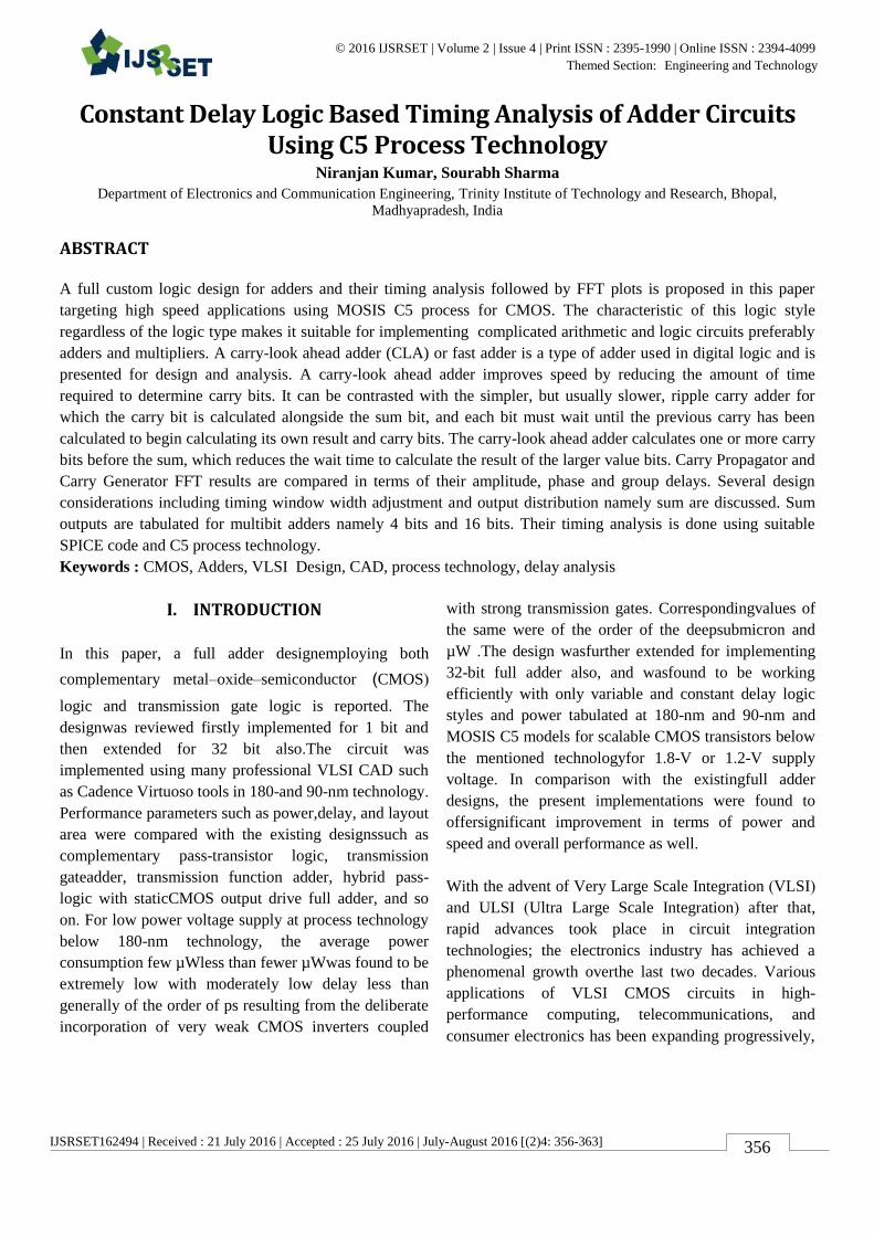
Figure 1. Abstraction Hierarchy for VLSI Adders 1
Our design methods usually differ by the number of
abstraction levels and the complexities involved.
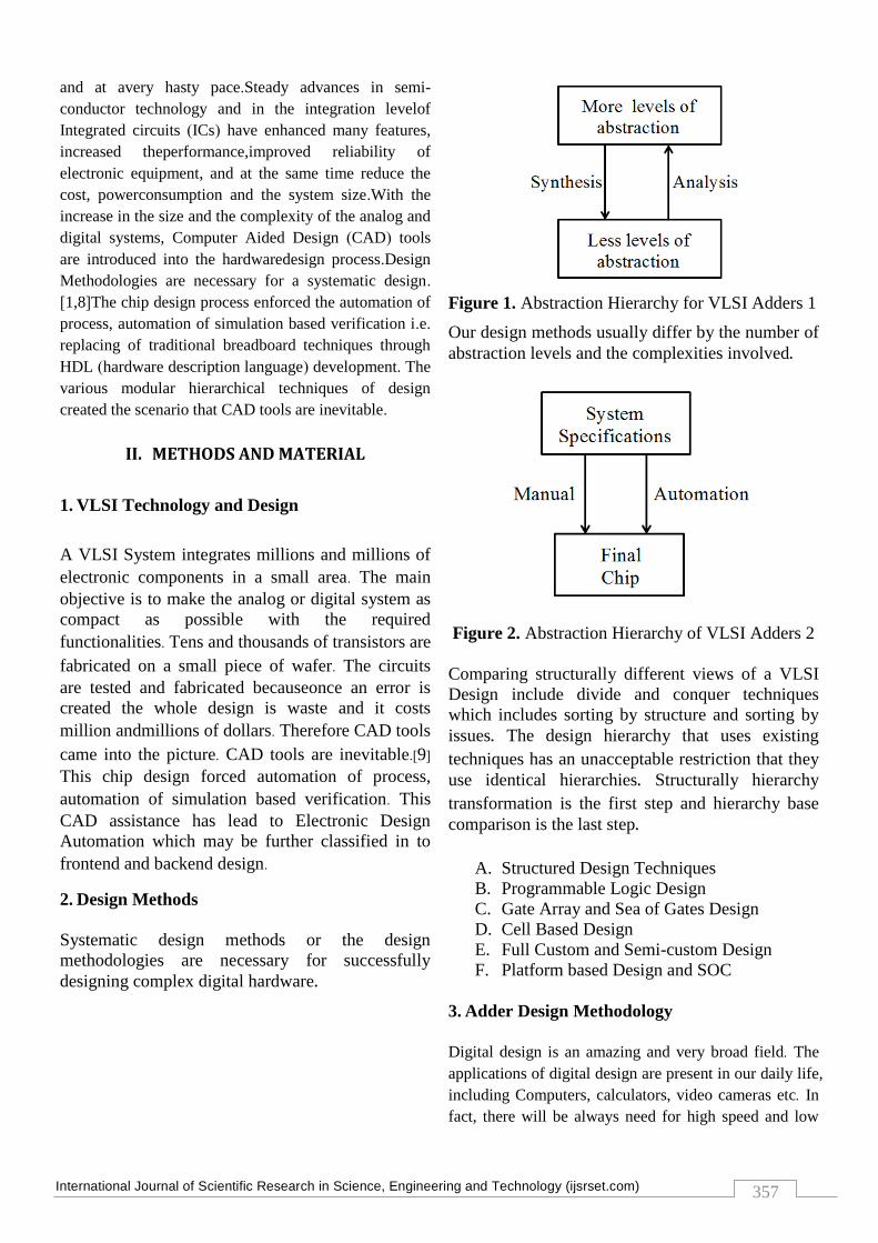
Figure 2. Abstraction Hierarchy of VLSI Adders 2
Comparing structurally different views of a VLSI
Design include divide and conquer techniques
which includes sorting by structure and sorting by
issues. The design hierarchy that uses existing
techniques has an unacceptable restriction that they
use identical hierarchies. Structurally hierarchy
transformation is the first step and hierarchy base
comparison is the last step.
A. Structured Design Techniques
B. Programmable Logic Design
C. Gate Array and Sea of Gates Design
D. Cell Based Design
E. Full Custom and Semi-custom Design
F. Platform based Design and SOC
3. Adder Design Methodology
Digital design is an amazing and very broad field. The
applications of digital design are present in our daily life,
including Computers, calculators, video cameras etc. In
fact, there will be always need for high speed and low

International Journal of Scientific Research in Science, Engineering and Technology (ijsrset.com)
358
power digital products which makes digital design a
future growing business. Adders are critical component
of a microprocessor and are the core component of
central processing unit. Furthermore, it is the heart of the
instruction execution portion of every computer. Adders
comprise the combinational logic that implements logic
operations, such as AND and OR, and arithmetic
operations, such as ADD and SUBTRACT.
Figure 3. Presented Methodology and Planning for
Adder Circuit design
Methodology and Planning of Work:
The design methodology can be clear from
following
1. Defining the requirements and setting the
specifications.
2. Design according to the Tool flow (EDA based).
3. Design of the Test circuits.
4. Simulating the Test results and optimization of
the parameters
The design methodology can be summarized as
1. Choosing the basic structure of the Adders.
2. Selection of the computational model using
appropriate process technology.
3. Measurement and Optimization of Design
parameters
4. Physical model implementationof the design.
III. RESULTS AND DISCUSSION
4. Simulation Results and Experimental Data
A regrious effort has been to implement the
presented design. The presented design isa full
custom integrated circuit design with all design
rules and network consistency
Checks verified. The project aims to design the
combinational circuits and simulatethe designed
circuits. The designed schematic views and icon
views along with thesimulation results are shown
one by one along with one final integrated design.
AnNCC (Network consistency check) report is
attached for the complete design.
There are numerous topologies and designs exist in
literature. This paper presents a full custom design
of multi bit adders and simulation results are as
shown
Figure 4.1. Schematic and icon view of1 bit half
adder
Figure 4.2. Schematic and icon view of 1 bit Full
adder
Figure 4.3. icon view of 1 bit Full adder with
signals marked
International Journal of Scientific Research in Science, Engineering and Technology (ijsrset.com)
359
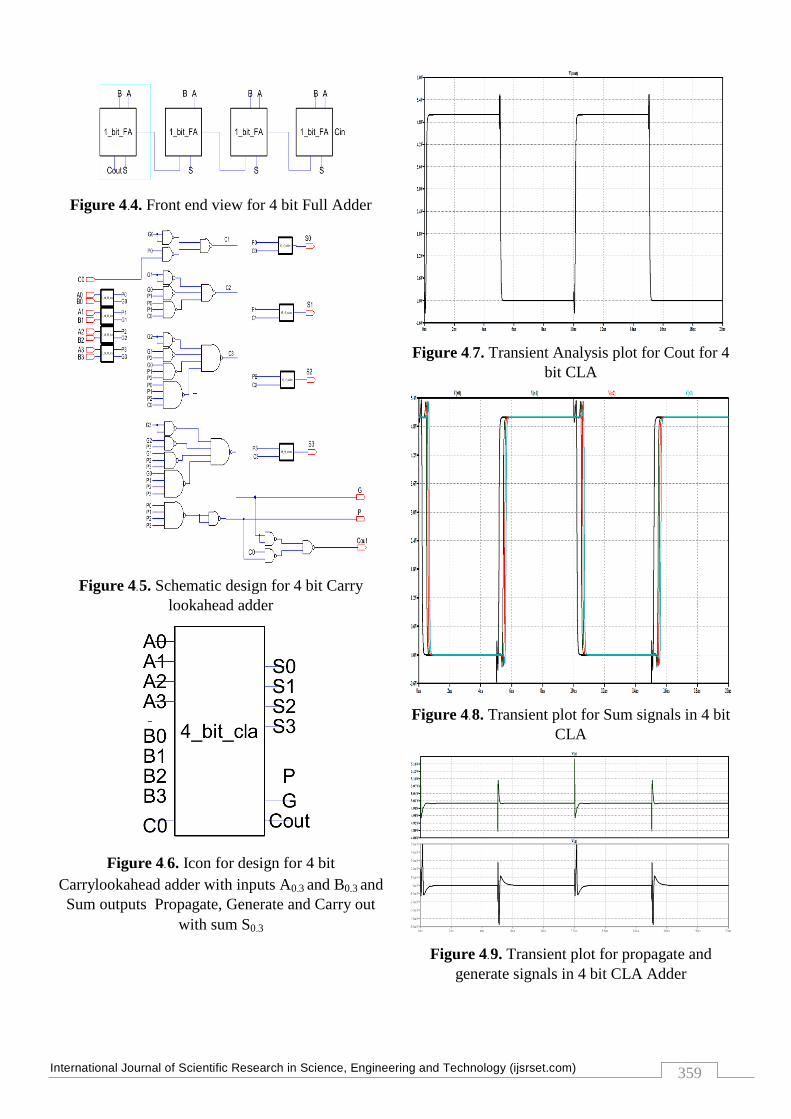
Figure 4.4. Front end view for 4 bit Full Adder
Figure 4.5. Schematic design for 4 bit Carry
lookahead adder
Figure 4.6. Icon for design for 4 bit
Carrylookahead adder with inputs A0-3 and B0-3 and
Sum outputs Propagate, Generate and Carry out
with sum S0-3
Figure 4.7. Transient Analysis plot for Cout for 4
bit CLA
Figure 4.8. Transient plot for Sum signals in 4 bit
CLA
Figure 4.9. Transient plot for propagate and
generate signals in 4 bit CLA Adder
International Journal of Scientific Research in Science, Engineering and Technology (ijsrset.com)
360
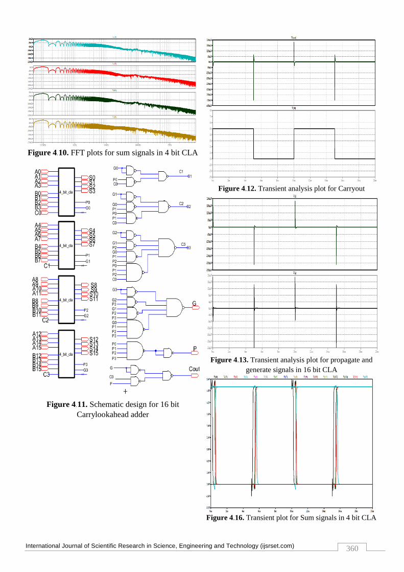
Figure 4.10. FFT plots for sum signals in 4 bit CLA
Figure 4.11. Schematic design for 16 bit
Carrylookahead adder
Figure 4.12. Transient analysis plot for Carryout
Figure 4.13. Transient analysis plot for propagate and
generate signals in 16 bit CLA
Figure 4.16. Transient plot for Sum signals in 4 bit CLA

International Journal of Scientific Research in Science, Engineering and Technology (ijsrset.com)
361
Figure 4.17. FFT plots or Noise index plot for Sum
Signals in 16 bit CLA design
5. FFT plots comparison between 4 bit CLA and 16
bit CLA
The performance analysis of adders 4 bits and 16 bits in
terms of their FFT profile is shown in above section and
tabulation and comparison of FFT and transient
parameters is illustrated here and drawn in table- 1,
shows different,. thus, there exist tradeoffbetween these
parameters. the results are helpful in selectionof an
adder according to desired result and application.
Table 1
FFT Index Results for 4 bit CLA (Sum Signals)
FFT plot parameters for signal S0
S.No. Frequency Magnitude Delay
1. 10MHz 94.59 dB 213.17 ps
100 MHz 6.27 dB 49.76 ns
1 GHz 94.46 dB 1.01 ns
10 GHZ 100.16 dB 203.09 ps
100 GHz 111.9 dB 179.90 ps
FFT plot parameters for signal S1
2. Frequency Magnitude Delay
10MHz 91.13 dB 522.8 ps
100 MHz 6.27 dB 7.82 ns
1 GHz 91.24 dB 486.96 ps
10 GHZ 102.49 dB 551.8 ps
100 GHz 115.57 dB 567.45 ps
FFT plot parameters for signal S2
3. Frequency Magnitude Delay
10MHz 86.51 dB 603.75 ps
100 MHz 6.277 dB 49.30 ns
1 GHz 86.59 dB 2.85 ns
10 GHZ 96.32 dB 570.08 ps
100 GHz 12.43 dB 116.10 ps
FFT plot parameters for signal S3
4. Frequency Magnitude Delay
10MHz 81.8 dB 698.35 ps
100 MHz 6.277 dB 49.20 ns
1 GHz 81.88 dB 3.04 ns
10 GHZ 88.53 dB 677.06 ps
100 GHz 109.98 dB 808.22 ps
Table 2
FFT Index Results for 16 bit CLA (Sum Signals)
FFT plot parameters for signal S0
S.No. Frequency Magnitude Delay
1. 100MHz 6.99 dB 4.78 ns
1THz 127.32 dB 2.5 ns
FFT plot parameters for signal S1
2. Frequency Magnitude Delay
100MHz 6.96 dB 4.46 ns
1THz 131.55dB 457.57 ps
FFT plot parameters for signal S2
3. Frequency Magnitude Delay
100MHz 6.99 dB 4.39 ns
1THz 131.36 dB 2.7 ns
FFT plot parameters for signal S3
4. Frequency Magnitude Delay
100MHz 7.02 dB 575.40ps
1THz 138.157 dB 1.05 ns
FFT plot parameters for signal S4
Frequency Magnitude Delay
5. 100MHz 149.10 149.89 ps
1THz 166.049 dB 1.89 ns
FFT plot parameters for signal S5
6. Frequency Magnitude Delay
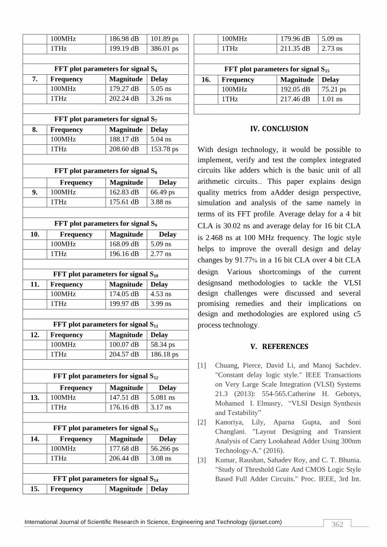
International Journal of Scientific Research in Science, Engineering and Technology (ijsrset.com)
362
100MHz 186.98 dB 101.89 ps
1THz 199.19 dB 386.01 ps
FFT plot parameters for signal S6
7. Frequency Magnitude Delay
100MHz 179.27 dB 5.05 ns
1THz 202.24 dB 3.26 ns
FFT plot parameters for signal S7
8. Frequency Magnitude Delay
100MHz 188.17 dB 5.04 ns
1THz 208.60 dB 153.78 ps
FFT plot parameters for signal S8
Frequency Magnitude Delay
9. 100MHz 162.83 dB 66.49 ps
1THz 175.61 dB 3.88 ns
FFT plot parameters for signal S9
10. Frequency Magnitude Delay
100MHz 168.09 dB 5.09 ns
1THz 196.16 dB 2.77 ns
FFT plot parameters for signal S10
11. Frequency Magnitude Delay
100MHz 174.05 dB 4.53 ns
1THz 199.97 dB 3.99 ns
FFT plot parameters for signal S11
12. Frequency Magnitude Delay
100MHz 100.07 dB 58.34 ps
1THz 204.57 dB 186.18 ps
FFT plot parameters for signal S12
Frequency Magnitude Delay
13. 100MHz 147.51 dB 5.081 ns
1THz 176.16 dB 3.17 ns
FFT plot parameters for signal S13
14. Frequency Magnitude Delay
100MHz 177.68 dB 56.266 ps
1THz 206.44 dB 3.08 ns
FFT plot parameters for signal S14
15. Frequency Magnitude Delay
100MHz 179.96 dB 5.09 ns
1THz 211.35 dB 2.73 ns
FFT plot parameters for signal S15
16. Frequency Magnitude Delay
100MHz 192.05 dB 75.21 ps
1THz 217.46 dB 1.01 ns
IV. CONCLUSION
With design technology, it would be possible to
implement, verify and test the complex integrated
circuits like adders which is the basic unit of all
arithmetic circuits... This paper explains design
quality metrics from aAdder design perspective,
simulation and analysis of the same namely in
terms of its FFT profile. Average delay for a 4 bit
CLA is 30.02 ns and average delay for 16 bit CLA
is 2.468 ns at 100 MHz frequency. The logic style
helps to improve the overall design and delay
changes by 91.77% in a 16 bit CLA over 4 bit CLA
design. Various shortcomings of the current
designsand methodologies to tackle the VLSI
design challenges were discussed and several
promising remedies and their implications on
design and methodologies are explored using c5
process technology.
V. REFERENCES
[1] Chuang, Pierce, David Li, and Manoj Sachdev.
"Constant delay logic style." IEEE Transactions
on Very Large Scale Integration (VLSI) Systems
21.3 (2013): 554-565.Catherine H. Gebotys,
Mohamed I. Elmasry, “VLSI Design Synthesis
and Testability”
[2] Kanoriya, Lily, Aparna Gupta, and Soni
Changlani. "Layout Designing and Transient
Analysis of Carry Lookahead Adder Using 300nm
Technology-A." (2016).
[3] Kumar, Raushan, Sahadev Roy, and C. T. Bhunia.
"Study of Threshold Gate And CMOS Logic Style
Based Full Adder Circuits." Proc. IEEE, 3rd Int.
International Journal of Scientific Research in Science, Engineering and Technology (ijsrset.com)
363
Conference on Electronics and Communication
Systems (ICECS), IEEE. 2016.
[4] Babu, Hima, P. Maria Glenny, and Anto Yohan.
"Comparison of Power and Area: 2 Bit Hybrid
Fulladder Design With 2 Bit Full Adder Using
CMOS Technology." Imperial Journal of
Interdisciplinary Research 2.4 (2016).
[5] Senthilkumaran, K., and K. R. Kashwan.
"Adiabatic constant delay logic style." Innovations
in Information, Embedded and Communication
Systems (ICIIECS), 2015 International
Conference on. IEEE, 2015.
[6] Bhattacharyya, Partha, et al. "Performance
analysis of a low-power high-speed hybrid 1-bit
full adder circuit." IEEE Transactions on very
large scale integration (VLSI) systems 23.10
(2015): 2001-2008.
[7] Anku Bala “Layout and Design Analysis of Carry
Look Ahead Adder Using 90nm Technology”,
Int.Journal Of Electrical & Electronics Engg.
Volume 2, spl..issue1, 2015.
[8] Amuthavalli G. and Gunasundari R, “Analysis Of
16-Bit Carry Look Ahead Adder – A Subthreshold
Leakage PowerPerspective”, ARPN Journal of
Engineering and Applied Sciences Volume-10,
NO. 6, April 2015.
[9] V. Reethika Rao, Dr. K. Ragini, “Comparative
Analysis Of 32 Bit Carry Look Ahead Adder
using Constant Delay Logic”, International
Journal of Science, Engineering and Technology
Research (IJSETR), Volume 3, Issue 10, October
2014.
[10] V. Reethika Rao, Dr. K. Ragini, “Comparative
Analysis Of 32 Bit Carry Look Ahead Adder
using Constant Delay Logic”,International Journal
of Science, Engineering and Technology Research
(IJSETR), Volume 3, Issue 10, October 2014.
[11] Jagannath Samanta, Mousam Halder, Bishnu
Prasad De, “Performance Analysis of High Speed
Low Power Carry LookAhead Adder Using
Different Logic Styles”, International Journal of
Soft Computing and Engineering (IJSCE),
Volume-2,Issue-6, Jan- 2013.
[12] R.Kathiresan, Dr. M.Thangavel, K.Rathinakumar,
S.Maragadharaj, “Analysis Of Different Bit Carry
Look Ahead AdderUsing Verilog Code”,
International Journal of Electronics and
Communication Engineering &
Technology(IJECET), Volume4, Issue 4, July-
August, 2013.
[13] Jatinder Kumar, Parveen Kaur, “Comparative
Performance Analysis of Different CMOS Adders
Using 90nm and 180nm Technology”,
International Journal of Advanced Research in
Computer Engineering & Technology (IJARCET)
Volume 2Issue 8, August 2013.
[14] Computer aids for VLIS http://www.
rulabinsky.com/steve
AUTHOR’S PROFILE
Mr. Niranjan Kumar has
obtained his Bachelor of
Engineering in Electronics and
Telecommunication
Engineering) degree from
RTMNU University Nagpur
(Maharashtra) India in 2013.
He is perusing Master of
Technology in VLSI from
Rajiv Gandhi Technological
University, Bhopal (M.P.)
India.