constraint driven design using orcad® pcb design tools · –the pcb designer can concentrate on...
TRANSCRIPT

©2010 Nordcad Systems A/S
Rev 1.00
Constraint driven design using OrCAD® PCB design tools

©2010 Nordcad Systems A/S – Revision 1.00
About the author
• Ole Ejlersen, CTO
– Nordcad Systems A/S a Cadence® Channel Partner
– Master in Electronics Engineering
– 14+ years in EDA industry working with and serving the
Danish industry.
– www.nordcad.dk
• Work tasks
– Hotline support, training and services for Cadence
software in Denmark
– Startup service to companies adopting Cadence tools.
– Great experience in building a solid constraint driven hw
development flow
– Skill programming
– Danish technical newsletter e-SERVICE with tips and
tricks, movies etc.
– Presentation and demonstration of EDA software from
Cadence.
2

©2010 Nordcad Systems A/S – Revision 1.00
Agenda
• Introduction
• Control constraints using Cadence®
OrCAD® PCB Design tools
– Flow
– Basic principle & goal
– Constraint overview
– From Capture to PCB Editor
– Build constraint template– Example
– User your constraint template
– Constraint matchup principle
– Finalizing the PCB
• Wrapup
• Appendices
– Identify critical nets
– Constraint Hierarchy
• Q&A
3
• What is a constraint driven flow?
– Automated communication of design
intent

©2010 Nordcad Systems A/S – Revision 1.00
Are you confused ????
4
@
POST IT
Schematic Entry
/
Signal Integrity
/
A/D Simulation
• Passing constraints
• Plenty information channels
• Lots of information
• Many sources
• Is the information contradicting
• Is the design ”over constrained”
• Could there be a reason if the result is
far from optimum?

©2010 Nordcad Systems A/S – Revision 1.00
Make it simple and efficient!
5
@/file(s)
Schematic Entry
/
Signal Integrity
/
A/D Simulation
• Communication – made simple and efficient
• Let’s talk the same ”language”
• What You Communicate Is What You Get
(WYCIWYG)

©2010 Nordcad Systems A/S – Revision 1.00
Optimize the flow
• Standardize constraint communication
– Build constraint standards
– Pass constraints from Schematic to
PCB
– Specify constraints early in the design
process
• Review functionality
– Cross-probing
– Measure and review constraints
– Reports
– DRC check and design status
– Extract to SI Analysis
6
Pass
Constraints
PCB Design (Internal/External)
/
PCB Review with SI analysis and Crossprobing
Schematic Entry
/
Signal Integrity
/
A/D Simulation
©2010 Nordcad Systems A/S – Revision 1.00
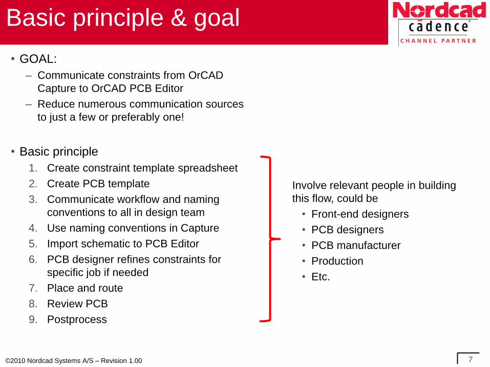
Basic principle & goal
• GOAL:
– Communicate constraints from OrCAD
Capture to OrCAD PCB Editor
– Reduce numerous communication sources
to just a few or preferably one!
• Basic principle
1. Create constraint template spreadsheet
2. Create PCB template
3. Communicate workflow and naming
conventions to all in design team
4. Use naming conventions in Capture
5. Import schematic to PCB Editor
6. PCB designer refines constraints for
specific job if needed
7. Place and route
8. Review PCB
9. Postprocess
7
Involve relevant people in building
this flow, could be
• Front-end designers
• PCB designers
• PCB manufacturer
• Production
• Etc.

©2010 Nordcad Systems A/S – Revision 1.00
Constraint overview
8
• All constraints are controlled using Constraint Manager in PCB Editor
– Physical– Line width, via types, routing layers
– Spacing (and same-net-spacing)– Line to line, via to line, pin to via etc.
– Electrical (available in Allegro PCB Design Performance Option and higher)– Matched length, differential pairs etc.
• Constraint Sets (CSets) – what are they
– Collection of constraints (e.g., width, via type, layers)
• Default: 0.2mm width, via60h25, route on all layers
• 50ohm: 0.32mm on outer layers, 0.3mm on inner layers
– Comparable to Microsoft Word styles
• Heading 1: Arial 15, Bold, font color red
– 3 types: Physical, Spacing and Electrical
– Nets and Netclasses can refer to a Constraint Set
– Will inherit constraints from referred Cset

©2010 Nordcad Systems A/S – Revision 1.00
From Capture to PCB Editor
9
• Capture communicates with PCB Editor through a netlist
– Components and component/function/pin properties
– Nets and net properties
• Important net properties
– ’Net_physical_type’ – property name added to net → Net is added to Physical Netclass
– Physical Netclass can reference Physical Constraint Set (PCset)
– ’Net_spacing_type’– property name added to net → Net is added to Spacing Netclass
– Spacing Netclass can reference Spacing Constraint Set (SCset)
– ’Electrical_constraint_set’– property name added to net → Net refers directly to Electrical Constraint Set (ECSet)
GND: net_physical_type=power
GND: net_spacing_type=power
WR: Electrical_constraint_set=50ohm
PCB EditorCapture
Capture to PCB Editor netlist
Netclass
”Power”
Constraint Manager
SCSet
PCSet
ECSet
Netclass
”Power”
Notice: nets without– Net_spacing_type
– Net_physical_type
– Electrical_constraint_set
uses default Constraint Set

©2010 Nordcad Systems A/S – Revision 1.00
Build your constraint template
• Create a spreadsheet with standard constraint
specifications
– Netclass names
– Constraint set names and key constraint values
• Create an empty PCB design (template) with
– Constraints sets: spacing, physical (and electrical)
– Netclasses
• Create the necessary relations between
netclasses and constraint sets
10
Net_Physical_Type Width Via type
<None> 0.2mm via26
Power 0.5mm via40
AD 0.1mm via26
Constraint Sets in PCB Editor
01mm 0.1mm via26
02mm 0.2mm via26
05mm 0.5mm via40
Via names Size Hole
Via40 1mm 0.6mm
Via26 0.7mm 0.3mm
via75 2mm 1mm

©2010 Nordcad Systems A/S – Revision 1.00
Example spreadsheets
11
Net_Physical_Type Width Via type
<None> 0.2mm via26
Power 0.5mm via40
AD 0.1mm via26
Constraint Sets in PCB Editor
01mm 0.1mm via26
02mm 0.2mm via26
05mm 0.5mm via40
Via names Size Hole
Via40 1mm 0.6mm
Via26 0.7mm 0.3mm
via75 2mm 1mm
Physical constraint setup
Net_Spacing_Type <None> Power AD
<None> 0.2mm 0.5mm 0.2mm
Power 0.5mm 0.5mm
AD 0.1mm
Constraint Sets in PCB Editor L-L L-S V-S V-V V-P
01mm 0.1mm 0.1mm 0.1mm 0.1mm 0.1mm
02mm 0.2mm 0.2mm 0.2mm 0.2mm 0.2mm
05mm 0.5mm 0.5mm 0.5mm 0.5mm 0.5mm
Legend Type Description
L Line Track/cline
P Pin Component pin
S Shape Copper pour/area
V Via
Spacing constraint setup
Electrical CSets Constraints Constraint
50Ohm Impedance 50Ω
55Ohm Impedance 55Ω
DDR2_Addr Wiring Topology
Impedance 50Ω
Matchgroup Matched length
DDR2_CLK Wiring Topology
Diff impedance 100Ω
Electrical constraint setup
Individual Constraints (e.g. property
‘Min_line_width’) overwrites other constraints!
• These are just examples
– Build to fit your needs!
• Communicate to schematic designers
– They should use correct Netclass names
©2010 Nordcad Systems A/S – Revision 1.00
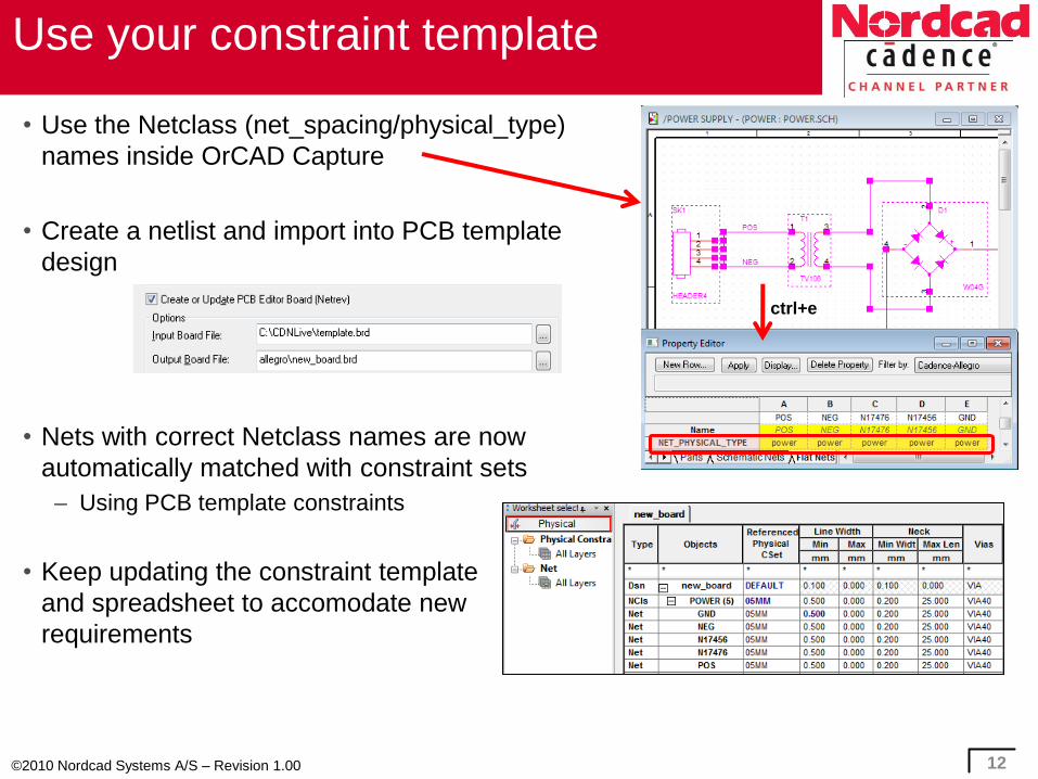
Use your constraint template
• Use the Netclass (net_spacing/physical_type)
names inside OrCAD Capture
• Create a netlist and import into PCB template
design
• Nets with correct Netclass names are now
automatically matched with constraint sets
– Using PCB template constraints
• Keep updating the constraint template
and spreadsheet to accomodate new
requirements
12
ctrl+e

©2010 Nordcad Systems A/S – Revision 1.00
Constraint matchup
13
Import netlist in template
Net_spacing_type?No Use default spacing
constraints
Include net in
predefined Spacing
Netclass and use
constraints assigned
to this netclass
Yes
Net_physical_type?
Yes
No
Include net in
predefined Physical
Netclass and use
constraints assigned
to this netclass
Yes
Electrical_constraint_set?No
No Use default physical
constraints
Yes
Assign net
Electrical_constraint_set
Yes
Constraint matchup
complete
NoDo not assign ECSet
Notice: nets without– Net_spacing_type
– Net_physical_type
– Electrical_constraint_set
uses default Constraint Set

©2010 Nordcad Systems A/S – Revision 1.00
Finalizing the PCB
• After constraint matchup
– PCB Designer refines the constraints if
necessary
– Finish up the PCB (place, route etc.)
• Review using standard functionality
– Cross-probing from Capture to PCB
Editor to highlight elements
– Display→ Status (DRC update/check)
– Display → Constraints
– Extract to SigXplorer for SI analysis
14

©2010 Nordcad Systems A/S – Revision 1.00
What are the benefits
• Control the design flow– Default constraints are part of the PCB template
– Use of the correct names during schematic entry automates most of the constraint setup
– The PCB Designer can concentrate on primary tasks since constraints are passed using a
standardized methodology
– Constraints can be reused and a library of verified constraints is built
– Running Design Rule Check verifies the passed constraints
– All designers talk the same language– makes designing much easier
– documentation is more consistent
– Constraint review is easier and faster
– Less errors due to consistency throughout the flow – What You Communicate Is What You Get
(WYCIWYG)
• Questions?
15

©2010 Nordcad Systems A/S – Revision 1.00 16
©2010 Nordcad Systems A/S – Revision 1.00
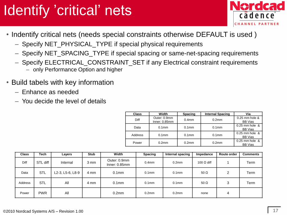
Identify ’critical’ nets
• Indentify critical nets (needs special constraints otherwise DEFAULT is used )
– Specify NET_PHYSICAL_TYPE if special physical requirements
– Specify NET_SPACING_TYPE if special spacing or same-net-spacing requirements
– Specify ELECTRICAL_CONSTRAINT_SET if any Electrical constraint requirements– only Performance Option and higher
• Build tabels with key information
– Enhance as needed
– You decide the level of details
17
Class Width Spacing Internal Spacing Via
DiffOuter: 0.9mm
Inner: 0.85mm0.4mm 0.2mm
0.25 mm hole &
BB Vias
Data 0.1mm 0.1mm 0.1mm0.25 mm hole &
BB Vias
Address 0.1mm 0.1mm 0.1mm0.25 mm hole &
BB Vias
Power 0.2mm 0.2mm 0.2mm0.25 mm hole &
BB Vias
Class Tech Layers Stub Width Spacing Internal spacing Impedance Route order Comments
Diff STL diff Internal 3 mmOuter: 0.9mm
Inner: 0.85mm0.4mm 0.2mm 100 Ω diff 1 Term
Data STL L2-3, L5-6, L8-9 4 mm 0.1mm 0.1mm 0.1mm 50 Ω 2 Term
Address STL All 4 mm 0.1mm 0.1mm 0.1mm 50 Ω 3 Term
Power PWR All 0.2mm 0.2mm 0.2mm none 4