contact resistance of ti-si-c-ag and ti-si-c-ag-pd...
TRANSCRIPT
Contact resistance of Ti-Si-C-Ag and Ti-Si-C-
Ag-Pd nanocomposite coatings
Niklas Gunnarsson Sarius, Jonas Lauridsen, E. Lewin, U. Jansson, Hans Högberg, Å. Öberg,
P. Leisner, Per Eklund and Lars Hultman
Linköping University Post Print
N.B.: When citing this work, cite the original article.
Personal use of this material is permitted. However, permission to reprint/republish this
material for advertising or promotional purposes or for creating new collective works for
resale or redistribution to servers or lists, or to reuse any copyrighted component of this work
in other works must be obtained from the IEEE.
Niklas Gunnarsson Sarius, Jonas Lauridsen, E. Lewin, U. Jansson, Hans Högberg, Å. Öberg,
P. Leisner, Per Eklund and Lars Hultman, Contact resistance of Ti-Si-C-Ag and Ti-Si-C-Ag-
Pd nanocomposite coatings, 2012, Journal of Electronic Materials, (41), 3, 560-567.
http://dx.doi.org/10.1007/s11664-011-1813-8
Copyright: Springer Verlag (Germany) / Institute of Electrical and Electronics Engineers
(IEEE)
http://www.ieee.org/index.html
Postprint available at: Linköping University Electronic Press
http://urn.kb.se/resolve?urn=urn:nbn:se:liu:diva-63625

1
Contact resistance of Ti-Si-C-Ag and
Ti-Si-C-Ag-Pd nanocomposite coatings
N. G. Sarius
a,b,c, J. Lauridsen
c, E. Lewin
d*, U. Jansson
d, H. Högberg
c, Å. Öberg
e,
G. Sarovaf, G. Staperfeld
f, P. Leisner
a,b, P. Eklund
c, L. Hultman
c
aSP Technical Research Institute of Sweden, Box 857, 501 15 Borås, Sweden,
Phone: +4610-5165702, fax: +4636-166180, [email protected].
bMaterials and Manufacturing,
School of Engineering, Jönköping University, Box 1026, SE-551 11
Jönköping, Sweden.
cThin Film Physics Division, Department of Physics,Chemestry, and Biology, IFM, Linköping
University, SE-58183 Linköping, Sweden.
dDepartment of Materials Chemistry, The Ångström Laboratory, Uppsala University, Box 524, SE-751
20 Uppsala, Sweden.
eABB Corporate Research, Forskargränd 7, SE-721 78 Västerås, Sweden.
f Harting, Corporate Technology Services, Marienwerderstrasse 3, 32339 Espelkamp, Germany.
* Present address: Laboratory for Nanoscale Materials Science, EMPA,
Überlandstrasse 129, CH-8600 Dübendorf, Switzerland.

2
Abstract
Ti-Si-C-Ag-Pd and Ti-Si-C-Ag nanocomposite coatings were deposited by direct current magnetron
sputtering on Cu substrates with an electroplated Ni layer. Analytical electron microscopy, x-ray
diffraction and x-ray photoelectron spectroscopy show that the nanocomposites consist of TiC, Ag:Pd,
and amorphous SiC. The contact resistance of these coatings against a spherical Au-Co surface was
measured for an applied contact force up to 5 N. Ti-Si-C-Ag-Pd coatings with an Ag:Pd top coating has
~10 times lower contact resistance at contact forces below 1 N (~10 mΩ at ~0.1 N), and 2-3 times
lower for contact forces around 5 N (<1 mΩ at 5 N), compared to the Ti-Si-C-Ag coating.
Keywords: titanium carbide; nanocomposite; physical vapor deposition (PVD); contact resistance;
Surface roughness; silver palladium.
3
1. Introduction
Ti-C based nanocomposites show promise to replace Au [1-9] in electrical contact applications, as a
material with complementary tribological qualities [10-16]. Ti-Si-C [4,7] and Ti-Si-C-Ag [5,6]
nanocomposite coatings thus exhibit low contact resistance and resistivity values. Typical electrical
contacts consist of a conductor of Cu coated with electroplated Ni between the Ti-Si-C based
nanocomposite coating and the conductor [17]. The purpose of the Ni layer is to hinder Cu from
diffusing to the surface of the contact and to serve as a load support for the contact coating. Surface
roughness of different Cu substrates can differ and thus influence the contact resistance. Importantly,
the contact resistance decreases for increased surface roughness, which is due to increased mechanical
breaking and penetration of surface oxides [18]. Electroplating of a surface can reduce the surface
roughness by leveling of the deposited surface, therefore it is interesting to compare surfaces deposited
with low and high effect of leveling, i.e., different Ni thicknesses.
In the present work, we have investigated Ti-Si-C-Ag:Pd electrical contact coatings for applications at
low contact forces. Ti-Si-C-Ag which has been investigated by Eklund [5] and Lauridsen [6] was
chosen as a reference coating for the tests, to compare the impact of Pd in the coating. To reduce the
contact resistance we considered a thin noble metal top coating on the nanocomposite. Ag might appear
as a first candidate for such a top coating, but since Ag alone can result in both sulfidizing and
migration, Ag was mixed with Pd since it is known to reduce the sulfidizing [19, 20] and migration
[21] effect of Ag.
The Ti-Si-C-Ag-Pd nanocomposite with a Ag-Pd top coating and Ti-Si-C-Ag coatings were coated on
Ni layers of different thickness, in order to investigate wether the electroplating leveling effect on the
surface roughness affects the contact resistance.
2. Experimental Procedures
Samples used in this investigation, consist of Ni electroplated Cu substrates, deposited with Ti-Si-C-
Ag-Pd nanocomposite with an Ag-Pd top coating or a Ti-Si-C-Ag nanocomposite coating. Table 1
shows data of coatings, polishing, and surface roughness of the samples. 1.5 mm thick and 15 mm wide
4
Cu bands were electroplated with 2 µm and 20 µm Ni respectively, and cut into 10 mm pieces. Ti-Si-C-
Ag-Pd nanocomposite with an Ag-Pd top coating and Ti-Si-C-Ag were deposited separately on both 2
µm and 20 µm thick Ni for comparing the contact coatings and the influence of the leveling effect of
the thicker Ni layer. The first number of the sample notations stands for different substrate treatments
before magnetron sputtering of contact coatings, and the second number stands for deposited contact
coating, see Table 1. Table 2 shows the surface roughness of Au-Co balls used for contact resistance
measurements, and which type of Au-Co ball that is used in combination with each different sample
during the contact resistance measurements.
2.1 Ni barrier layers
Before electroplating of Ni, the Cu substrates were cleaned with 10 % Decon 90 dissolved in deionized
water, and etched for 60 s with 25 g/l ammonium peroxydisulfate ((NH4)2S2O8), dissolved in deionized
water.
The Cu substrates were deposited with electroplated Ni using a sulfamate electrolyte shown in Table 3.
Deposition of the Ni layer was performed at 0.7 A/dm2 for 850 s to get ~2 µm thick layers and 0.7
A/dm2 during 8500 s to get ~20 µm thick layers.
2.2 Ti-Si-C-Ag and Ti-Si-C-Ag-Pd nanocomposite contact coatings
Prior to deposition of the Ti-Si-C-Ag and Ti-Si-C-Ag-Pd, the samples were ion etched with Ar in the
sputtering chamber, in order to remove oxides from the Ni electroplated surfaces.
Ti-Si-C-Ag was deposited for 10 min to a thickness of approximately 1 µm with a substrate
temperature of 270 ºC and Ar at 5 mTorr. This coating was deposited in a industrial deposition system
with a Ti-Si-C-Ag compound target of the composition 3Ti:1Si:5C +20 at.% Ag, to serve as a reference
material. The same chamber system was used without opening to atmosphere between argon ion
etching and magnetron sputtering.
5
Ti-Si-C-Ag-Pd was deposited during 40 min to an approximately thickness of 0.8 µm with Ar at 10
mTorr, followed by deposition of Ag - 30 at.% Pd for 4 min to a thickness of approximately 0.2 µm
with Ar at 5 mTorr (i.e., the same total thickness as for the reference coating). Both coatings were
deposited at a substrate temperature of 270 ºC. A pilot plant deposition system as described in [5] was
used with two sources, one Ti3SiC2 compound target (see [22]) and one Ag-Pd target.
2.3 Surface roughness measurements
3-D surface roughness measurements were performed with optical measurements technique using
Alicona Imaging Infinite Focus IFM 1.4. Collected surface roughness data are Rz (average value of
maximum height between valleys and tops) and Rp (average value of the height between the mean line
and the maximum).
2.4 Electrical contact resistance measurements
Figure 1 shows a schematic drawing of the contact resistance measurement setup. The measurements
were performed with a spherical surface pressed against the test sample at first contact followed by an
increased contact force from 0 to 5 N. The spherical contact surface consisted of 0.5 µm thick Cu–6
wt.% Sn with a radius of 3 mm, electroplated with 2 µm Ni and 0.5 µm of Au-1 wt.% Co (hard gold).
Au-Co was used as a reference material since it is commonly used in electrical contacts, mostly due to
its higher hardness than pure Au.
Measurements of the contact resistance was performed with a DC current of 1 mA and maximum
voltage limit of 20 mV, and zero current voltage adjustment with a low frequency around 1 kHz, using
an Agilent 4338B milliohmmeter connected to a computer with software (ZLBSurface), which
controlled the contact force and measured the contact resistance. The contact force was measured using
a calibrated amplifier with bending beams, having a resolution of the 0.01 N. The force was applied
with a step size of 0.04 N from 0 to 5 N. Measurement data of the contact resistance and the contact
force was recorded at every step. The software was set to perform measurements at four different

6
locations on every sample, with a distance of 1 mm between each location, allowing the contact
surfaces to be in open position in between each four measurements. Contact resistance measurements
were performed with Au-Co balls and substrates according to table 2 in the substrate order 2:2, 3:2, 1:2,
4:2, 1:1, 2:1, 3:1, 4:1, and Au-Co.
2.5 Structural and compositional characterization
Scanning electron microscopy (SEM) analyses using secondary electron mode was performed with a
SEM LEO 1550 instrument. The electron beam was set to 2 kV for the SEM analyses and 20 kV during
the elemental mapping with energy dispersive x-ray spectroscopy (EDX). X-ray diffraction (XRD)
scans were obtained with a Cu Kα X-ray source in θ/2θ geometry. X-ray photoelectron spectroscopy
(XPS) was performed using a Physical Electronic Quantum 2000 ESCA Microprobe. Sputter depth
profiles were acquired from four selected samples, (1:1, 1:2, 5:1 and 5:2) with both contact coatings
deposited on the roughest and the smoothest substrates. The depths of the profiles were set so that the
Ag-Pd top coating was penetrated and a few sputter cycles were measured in the underlying
nanocomposite coating. The same settings were used for the Ti-Si-C-Ag coatings. Sputtering was
performed with 4 keV Ar+ ions rastered over a 2x2 mm
2 surface, while the analysis spot had a diameter
of 200 µm. Samples for cross-sectional transmission electron microscopy (TEM) was prepared with a
Zeiss 1540 EsB CrossBeam focused ion beam (FIB) using the lift out technique [23]. TEM imaging
and with EDX in scanning TEM (STEM) mode was made using a Tecnai G2 20 U-Twin 200 kV
FEGTEM.
3. Results and Discussion
3.1 Surface roughness
Table 1 shows surface roughness values Rz and Rp of Ti-Si-C-Ag and Ti-Si-C-Ag-Pd with Ag-Pd top
coating on Ni coated Cu substrates. The difference in surface roughness values Rz and Rp between

7
substrates polished with grade 4000 grinding paper and electropolished is small, but as expected trend
is towards lower Rz and Rp, values for the electropolished substrates.
3.2 Microstructure and Composition
The SEM images in Figure 2 show the surface of Ti-Si-C-Ag-Pd with Ag-Pd top coating deposited on
2 µm Ni electroplated on Cu substrates pretreated in a) and Ti-Si-C-Ag deposited on 2 µm Ni
electroplated on Cu substrates in b). Independent of surface roughness, the Ag-Pd top-coated samples
have a smoother surface morphology, while the Ti-Si-C-Ag samples have a more nodular surface
structure (Figure 2).
Figure 3 shows XRD scans of sample a) 1:1, and b) 1:2 for comparison of the Ag-Pd top coated Ti-Si-
C-Ag-Pd and the Ti-Si-C-Ag coatings deposited on both rough and smooth surfaces. Peaks of the Cu
substrate and the electroplated Ni diffusion barrier layers are observed. In the Ti-Si-C-Ag coatings 1:1,
both TiC and Ag peaks are present as expected [5, 6]. However, the Ag-Pd topcoated Ti-Si-C-Ag-Pd;
1:2, exhibited no TiC, Ag or Pd peaks. Instead peaks between Ag and Pd (111), (220) and (311) are
present in Figure 3, indicating the presence of an fcc solid solution of Ag-Pd as previously reported
[24-26]. This agrees with the Ag-Pd phase diagram that exhibits a fcc solid solution over the complete
compositional range at temperatures lower than 962 °C (melting temperature of Ag) [27]. Annealing
tests up to 600 ºC during 23 h of Pd on TiC has shown no interaction [28], while annealing at 1000 ºC
and higher results in Ti-Pd phases and free C formation [29]. This is consistent with the present results.
The Ti-Si-C-Ag coatings exhibit XPS spectra in agreement with previous studies by Eklund et al [5]
and Lauridsen et al [6]. In the bulk of the coatings the C1s peak is found at a binding energy of 282.5
eV, which indicates carbidic bonding with contributions from C-Si and C-Ti. These carbidic
contributions are confirmed by the binding energies of Ti2p3/2 (at 455.0 eV) and Ti2p1/2 (at 461.0 eV)
from Ti-C bonds and Si2s (at 151.8 eV) from Si-C bonding. The Ag3d5/2 peak is found at 368.5 eV,
which is slightly higher than previously reported for this material, and could be attributed to Ag in
metallic bonding [30]. Ag3d spectra cannot provide information regarding the presence of Ag-Si bond
in the coating or not, though there is no significant peak shift or broadening regarding transition from

8
Ag-Ag bonds to Ag-Si bonds [31]. It is known, however, that mixing in the Ag-Si system is very
limited, with no formation of metastable phases up to 400 ºC [31,32]. A more detailed analysis of the
bonding is not possible due to the limited resolution in the acquired spectra. Near the surface, the Ti-Si-
C-Ag coatings exhibit shifts in both Ti2p and Si2s peaks indicating oxidation of the material. Only
trace amounts of oxygen are found within the coatings.
The Ti-Si-C-Ag-Pd samples exhibit a similar XPS appearance as the Ti-Si-C-Ag coatings. The binding
energies of C1s, Ti2p, Si2s, and Ag3d are slightly shifted (283.3 eV, 454.8 eV, 151.0 eV, and 368.1
eV, respectively). This points to different stoichiometries within the phases of the nanocomposite.
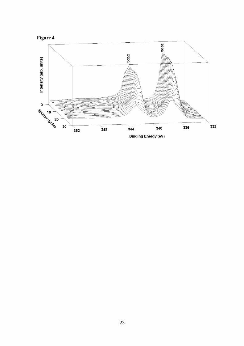
Figure 4 is an XPS sputter depth profile of Pd3d in the sample 1:2, through the Ag-Pd top coating and
into the Ti-Si-C-Ag-Pd nanocomposite. The Pd3d5/2 peak is found at 336.8 eV, which is consistent with
Pd bonded to Si, C or possibly O [30]. Some oxygen is found in the coating, but as the amount
continuously decreases from the interface between the nanocomposite and the top coat, it is probably
small in the bulk of the coating.
In the Ag-Pd top coating, there are considerable amounts of oxygen. The Ag3d5/2 peak is at the same
position as in the nanocomposite (368.1 eV), and the Pd3d5/2 is at 335.4eV (Figure 4); both peaks
indicating a metallic surrounding [30], which is consistent with the XRD results.
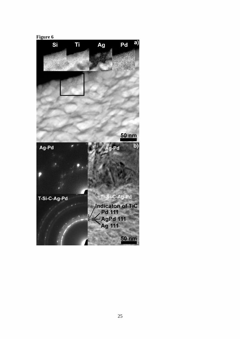
Figure 5 shows a cross-sectional TEM image of the Ag-Pd/Ti-Si-C-Ag-Pd/Ni sample. The Ti-Si-C-Ag-
Pd coating has a homogeneous structure of nm-size grains. Figure 6 shows a) STEM cross-sectional
image with EDX elemental maps of Si, Ti, Ag, and Pd, and b) cross-sectional TEM image and SAED
pattern from the same sample. The EDX maps indicate more Ag in locations of less Ti and vice versa.
Si and Pd are evenly distributed in the coating, but with slightly lower amounts at Ag-rich locations.
The SAED patterns in Figure 6 show one ring shifted from the 111 Ag and Pd ring locations to one 111
Ag-Pd alloy phase ring position confirming previous results [24], and the shift of the Ag and Pd peaks
to one Ag-Pd peak in the XRD scan (Figure 3). The SAED of Ag-Pd in the Ti-Si-C-Ag-Pd indicate
small crystals while the SAED of the Ag-Pd top coating indicate large crystals. SAED also shows that
the TiC is amorphous to nanocrystalline, as judged by the broad rings.
3.3 Contact resistance
9
Figures 7 and 8 are graphs showing contact resistance versus contact force between Au-Co and Ti-Si-
C-Ag nanocomposite coatings on 2 µm and 20 µm Ni, respectively, and Au-Co against Au-Co. Each
curve in figure 7 and 8, show the average contact resistance from four measurements, error bars show
maximum and minimum values. The figures show that the resistance at forces between 0 and 5 N is
lower for Au-Co against Au-Co than for Au-Co in contact with the Ti-Si-C-Ag nanocomposite. When
comparing the samples with 2 µm and 20 µm thick Ni layers, no influence can be found on the contact
resistance (see Figure 7 and 8). As can be seen in Figures 7 and 8 the contact resistance is
approximately 10 times higher for the Ti-Si-C-Ag nanocomposite against Au-Co than for Au-Co
against Au-Co at contact forces below 1 N. When the contact force increases the difference in contact
resistance decreases; at 5 N, the difference is less than a factor of 2.
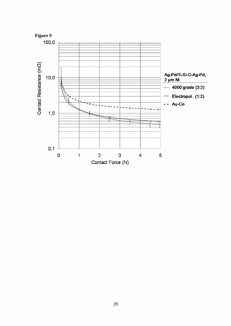
Figures 9 and 10 are graphs showing contact resistance versus contact force for Au in contact with Ag-
Pd/Ti-Si-C-Ag-Pd coating on 2 µm Ni, with different surface roughness, and for Au-Co against Au-Co.
The curves in Figure 9 and 10, each show the average contact resistance from four measurements, with
max and min error bars. The contact resistance is approximately the same for Ag-Pd/ Ti-Si-C-Ag-Pd as
for Au-Co in contact with Au-Co at low contact forces, but at 5 N the contact resistance is down to 0.5-
0.7 mΩ, which is lower for the Ag-Pd/Ti-Si-C-Ag-Pd in contact with Au-Co, than for Au-Co in contact
with Au-Co.
The large differences of 10 times higher contact resistance for the Ti-Si-C-Ag compared to the Ag-
Pd/Ti-Si-C-Ag-Pd and Au-Co coating at low contact forces below 1 N, is presumed to be caused by the
resistance of a thin oxide film covering the Ti-Si-C-Ag surface compared to Ag-Pd/Ti-Si-C-Ag-Pd, and
Au-Co where only small amounts of oxides are present. Increasing the contact force decreases the
influence of the oxide layer and around 5 N the difference in contact resistance is 2-3 times higher for
Ti-Si-C-Ag compared to Ag-Pd/Ti-Si-C-Ag-Pd and double compared to Au-Co in contact with Au-Co.
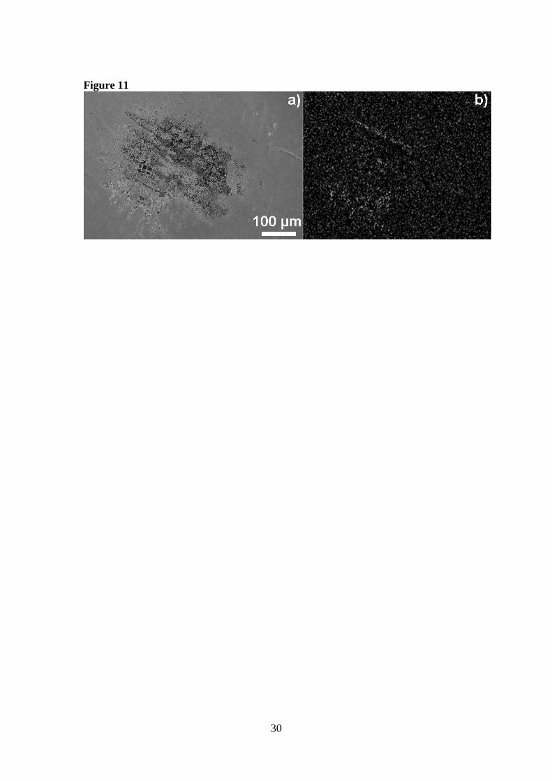
Figure 11 shows a) a SEM image, and b) a Ni Kα EDX mapping of the area the Au-Co ball number 4
in table 2 which has been in contact with the samples during contact resistance measurements. The Au
ball shows some degradation after contact resistance measurements when looking in SEM (Figure 11a).
It can also be seen in the EDX (Figure 11 b) that there is wear of the Au-Co with indications of Ni in

10
the mapping image. Mapping of the Au does, however, not indicate any areas without Au. It is
concluded that the Au-Co ball has not worn through the Au-Co coating.

11
4. Conclusions
The Ti-Si-C-Ag-Pd nanocomposite coatings grown by sputtering consist of Ag-Pd alloy nanocrystals
embedded in an amorphous to nanocrystaline matrix of Ti-C, Si-C, and Pd-Si or Pd-C. When adding Pd
into the Ti-Si-C-Ag system TiC growth is inhibited, and Pd also reduces the Ag crystal size, by serving
as a nucleation agent.
Ag-Pd/Ti-Si-C-Ag-Pd coatings have ~10 times lower contact resistance to Au-Co at contact forces
below 1 N compared to the Ti-Si-C-Ag in contact with Au-Co. For contact forces around 5 N, the
difference in contact resistance reduces to 2-3 times. At contact forces below 1 N the Ag-Pd/Ti-Si-C-
Ag-Pd has approximately the same contact resistance as Au-Co and at 5 N even lower contact
resistance than Au-Co, all coatings compared when in contact with Au-Co. The large difference at
contact forces below 1 N is caused by the presence of an oxide film on the Ti-Si-C-Ag surface
compared to the Ag-Pd/Ti-Si-C-Ag-Pd and the Au-Co.
It is also found that although there is a leveling effect by plating to 20 µm instead of 2 µm thickness,
there is no large corresponding influence from this smoothening on the contact resistance. This is most
likely due to the small difference of change in surface roughness.
Acknowledgments
We acknowledge Erik Olsson for technical assistance. The European EraSME Program, the Swedish
Knowledge Foundation, and The Swedish Board for Innovation Systems VINN Exellence Center on
Functional Nanostructured Materials (FunMat) supplied financial and analytical support.

12
References
[1] Å. Öberg, Å. Kassman, B. André, U. Wiklund, M. Lindqvist, E. Lewin, U. Jansson, H. Högberg,
T. Joelsson, H. Ljungcrantz, Eur. Phys. J. Appl. Phys. 49, 22902 (2010)
[2] P. Eklund, Surf. Eng. 23, 406 (2007)
[3] E. Lewin, E. Olsson, B. André, T. Joelsson, Å. Öberg, U. Wiklund, H. Ljungcrantz, U. Jansson,
Plasma Process. Polym. 6, S928 (2009)
[4] P. Eklund, J. Emmerlich, H. Högberg, O. Wilhelmsson, P. Isberg, J. Birch, P.O.Å. Persson,
U. Jansson, L. Hultman, J. Vac. Sci. Technol., B 23. 2486 (2005)
[5] P. Eklund, T. Joelsson, H. Ljungcrantz, O. Wilhelmsson, Z. Czigány, H. Högberg, L. Hultman,
Surf. Coat. Tech. 201, 6465 (2007)
[6] J. Lauridsen, P. Eklund, J. Jensen, H. Ljungcrantz, Å. Öberg,E. Lewin, U. Jansson, A. Flink,
H. Högberg, L. Hultman, Acta Materialia 58, 6592 (2010)
[7] J. Lauridsen, P. Eklund, T. Joelsson, H. Ljungcrantz, Å. Öberg,E. Lewin, U. Jansson, M. Beckers,
H. Högberg, L. Hultman, Surf. Coat. Technol. 205, 299 (2010)
[8] E. Lewin, B. André, S. Urbonaite, U. Wiklund, U. Jansson, J. of Mater. Chem. 20, 5950 (2010)
[9] E. Lewin, O. Wilhelmsson and U. Janson, J. of Appl. Phys. 100, 054303 (2006)
[10] U. Jansson, E. Lewin, M. Råsander, O. Eriksson, B. André, U. Wiklund, Surf. Coat. Technol.
(2010) doi:10.1016/j.surfcoat.2010.06.017

13
[11] J. Lin, J.J. Moore, W.C. Moerbe, M. Pinkas, B. Mishra, G.L. Doll, W.D. Sproul, J. Refr. Met.
Hard Mat. 28, 2 (2010)
[12] D. Martinez, C. Lopes-Cartes, A. Justo, A. Fernandez, J.C. Sanchez-Lopez, Solid State Sci. 11,
660 (2009)
[13] Y. T. Pei, D. Galvan, J. Th. M De Hosson, A. Cavaleiro, Surf. Coat. Tech. 198, 44 (2005)
[14] O. Wilhelmsson, M. Råsander, M. Carlsson, E. Lewin, B. Sanyal, U. Wiklund, O. Eriksson, U.
Jansson, Adv. Funct. Mater. 17, 1611 (2007)
[15] T. Zehnder, J. Matthey, P. Schwaller, A. Klein, P.-A. Steinmann, J. Patscheider, Surf. Coat. Tech.
238, 163 (2003)
[16] B. Feng, D.M Cao, W.J. Meng, J. Xu, R.C. Tittsworth, L-E. Rehn, P.M. Baldo, G.L. Doll, Surf.
Coat. Tech. 148, 153 (2001)
[17] N. G. Sarius, J. Lauridsen, E. Lewin, J. Lu, H. Högberg, Å. Öberg, H. Ljungcrantz, P. Leisner, P.
Eklund, L. Hultman, submitted for publication, included in N. G. Sarius' PhD thesis, Linköping
University, 2010, 1342, http://liu.diva-
-portal.org/smash/record.jsf?searchId=1&pid=diva2:381748&rvn=3
[18] E. Crinon, J. T. Evans, Mater. Sci. and Eng. A242, 121 (1998)
[19] M. Braunovic, V. V. Konchits, N. K. Myshkin, Electrical Contacts Fundamentals, Applications
and Technology, (CRC press Taylor & Francis Group, 2007), Ch 4
[20] M. Braunovic, V. V. Konchits, N. K. Myshkin, Electrical Contacts Fundamentals, Applications
and Technology, (CRC press Taylor & Francis Group, 2007) Ch 8

14
[21] R.J. Klein Wassink. Soldering in electronics, 2nd ed. (Electrochemical Publications Limited,
1989) Ch. 5
[22] P. Eklund, M. Beckers, U. Jansson, H. Högberg, L. Hultman, Thin Solid films 518, 1851 (2010)
[23] R.M. Langford, A.K. Petford-Long, J. Vac. Sci. Technol. A 19, 2186 (2001)
[24] F. Reniers, P. Delcambe, L. Binst, M. Jardinier-Offergeld, F. Bouillon, Thin Solid Film, 170, 41
(1989)
[25] C.-C.Yang, C.-C. Wan, Y.-Y. Wang, J. Colloid and Interface Science 279, 433 (2004)
[26] C.-Y. Huang, H.-J. Chiang, J.-C. Huang, S.-R. Sheen, NanoStructured Materials, 10, 1393 (1998)
[27] Binary Alloy Phase Diagrams, Ed. In Chief T. B. Massalski, (American Society for Metals, Metals
Park, Ohio, USA 1986)
[28] R. Wenzel, F. Goesmann, R. Schmid-Fetzer, Mater. Sci. Eng., B, Solid-State Mater. Adv. Technol.
52, 175 (1998)
[29] P. Demkowicz, K. Wright, J. Gan, D. Petti, Solid State Ionics, 179, 2313 (2008)
[30] J. Moulder, W. F. Stickle, P. E. Sobol, K. D. Bomben, Handbook of X-ray Photoelectron
Spectroscopy, Ed. J. Chastain, R.C.J. King, (Physical Electronics, Inc., Eden Prairie, USA, 1995)
[31] DK. Sarkar, S. Dhara, KGM. Nair, S. Chowdhury, Nucl. Instrum. Meth. Phys. Res B, 168, 215
(2000)
[32] SS. Lau, B. Y. Tsaur, M. von Allmen, JW. Mayer, D. Stritzker, CW. White, et al. Nucl. Instrum.
Meth. 97, 182 (1981)

15
Tables
Table 1. List of samples with layer architecture, surface roughness values, and contact resistance at contact forces of 1 and 5 N.
*Surface roughness values Rz is the average value of maximum height between valleys and tops, and Rp is the average value of the height between the mean line and the maximum. **Substrates were grinded with grade 4000 paper followed by electropolishing.
***Substrates was pretreated as “El polished*” before grinded with grade 4000 paper and 120 paper respectively.
Sample Rz*
(µm)
Rp*
(µm)
Contact coating Ni
thickness
(µm)
Cu substrate
polishing
Contact Force 1N Contact Force 5N
Contact resistance
mΩ Contact resistance
mΩ
1:1 0.72 0.42 Ti-Si-C-Ag 2 El polished** 9.00 1.71
1:2 1.03 0.56 Ag-Pd/Ti-Si-C-Ag-Pd 2 El polished** 1.26 0.58
2:1 0.34 0.24 Ti-Si-C-Ag 20 El polished** 8.34 1.67
2:2 0.43 0.22 Ag-Pd/Ti-Si-C-Ag-Pd 20 El polished** 1.31 0.62
3:1 0.74 0.48 Ti-Si-C-Ag 2 4000 grinded*** 8.43 1.72
3:2 1.16 0.63 Ag-Pd/Ti-Si-C-Ag-Pd 2 4000 grinded*** 1.3 0.46
4:1 0.45 0.24 Ti-Si-C-Ag 20 4000 grinded*** 6.89 1.56
4:2 0.59 0.37 Ag-Pd/Ti-Si-C-Ag-Pd 20 4000 grinded*** 1.63 0.68
Au-Co 0.53 0.40 Au-1 wt.% Co 2 None 2.15 1.21

16
Table 2. List of Au-Co balls used for contact resistance measurements with surface roughness values.
*Surface roughness values Rz is the average value of maximum height between valleys and tops, and Rp is the average value of
the height between the mean line and the maximum.
Au-Co
ball nr:
Rz*
(µm)
Rp*
(µm)
Rp/Rz
(µm)
Used for contact
resistance measurement
with sample
1 0.76 0.39 0.51 2:2, 3:2
2 0.94 0.63 0.67 1:2, 4:2,
3 0.42 0.18 0.44 1:1
4 0.57 0.34 0.59 2:1, 3:1, 4:1, Au-Co
17
Table 3. Recipe of Ni sulfamate electrolyte.
Nickel sulfamate Ni(NH2SO3)24H2O 310 g/l
Nickel chloride NiCl26H2O 31 g/l
Boric acid H3BO3 31 g/l
BP-N1 C10H8O9S3.3Na.xH2O 6.2 g/l
Sodium dodecyl sulfate CH3(CH2)11OSO3Na 0.25 g/l

18
Figure Captions
Figure 1. Schematic drawing of the contact resistance measurement set-up, showing where the current
(A) is applied and where the potential (V) is measured.
Figure 2. SEM images of Ti-Si-C-Ag-Pd contact coating with a Ag-Pd top coat (sample 1:2) in a) and
Ti-Si-C-Ag contact coating (sample 1:1) in b), both deposited on 2 µm Ni electroplated;
electropolished Cu.
Figure 3. XRD scan of samples a) 1:1(Ti-Si-C-Ag, electropolished), and b) 1:2 (Ag-Pd/Ti-Si-C-Ag,
electropolished).
Figure 4. XPS sputter depth profile of Pd3d in sample 1:2 (Ag-Pd/Ti-Si-C-Ag, electropolished).
Figure 5. Cross-sectional TEM image of the Ag-Pd/Ti-Si-C-Ag-Pd/Ni, sample 1:2 ((Ag-Pd/Ti-Si-C-
Ag, electropolished).
Figure 6. Cross-sectional a) STEM images of Si, Ti, Ag and Pd, and b) TEM image with SAED of Ag-
Pd and Ti-Si-C-Ag-Pd, of sample 1:2 (Ag-Pd/Ti-Si-C-Ag, electropolished).
Figure 7. Contact resistance versus contact force for Au-Co in contact with Ti-Si-C-Ag nanocomposite
on 2 µm Ni electroplated on Cu substrates pretreated to different surface roughnesses. Reference:
Au-Co in contact with Au-Co. Sample notations as given in Table 1.
Figure 8. Contact resistance versus contact force for Au-Co in contact with Ti-Si-C-Ag nanocomposite
on 20 µm Ni electroplated on Cu substrates pretreated to different surface roughnesses. Reference:
Au-Co in contact with Au-Co. Sample notations as given in Table 1.

19
Figure 9. Contact resistance versus contact force for Au-Co in contact with Ag-Pd/Ti-Si-C-Ag-Pd on 2
µm Ni electroplated on Cu substrates pretreated to different surface roughnesses. Reference: Au-Co in
contact with Au-Co. Sample notations as given in Table 1.
Figure 10. Graph showing contact resistance versus contact force for Au-Co in contact with Ag-Pd/Ti-
Si-C-Ag-Pd on 20 µm Ni electroplated on Cu substrates pretreated to different surface roughnesses.
Reference: Au-Co in contact with Au-Co. Sample notations as given in Table 1.
Figure 11. a) SEM image and b) Ni Kα EDX map of the contact area on Au-Co ball number 4 (table 2).
20
Figure 1

21
Figure 2
22
Figure 3
23
Figure 4

24
Figure 5
25
Figure 6

26
Figure 7

27
Figure 8
28
Figure 9

29
Figure
10
30
Figure 11