converter integration of high-voltage high-frequency sic
TRANSCRIPT
Converter Integration of High-Voltage
High-Frequency SiC Power Devices
Session: Medium-Voltage WBG Devices and Converters
Development for Advanced Distribution Grids

Outline of presentation
• HV SiC devices – 10kV MOSFET, 15kV MOSFET, 15kV
IGBT, 6.5kV JFET, 3.3kV - 5kV MOSFET
• What MV Power Conversion applications are enabled
• Grid integration of renewables
• High MW and MV Motor Drives
• FACTS and D-STATCOM applications
• Are these HV SiC devices easy to use – like 1.2kV/1.7kV
SiC MOSFET devices ?

Introduction
Traditional Power System Modern Power System Replacing 60 Hz Transformer
• Complex - large no. of variables
• Limited scope for control
• Non-linear loads
• Harmonics
• Lagging reactive power
• Penetration of renewables
• Power electronic converters
• dc-ac
• ac-ac
• Increased controllability
• Energy Control Center
• Solid State Transformer
• Power Electronic
Transformer
• Intelligent Transformer
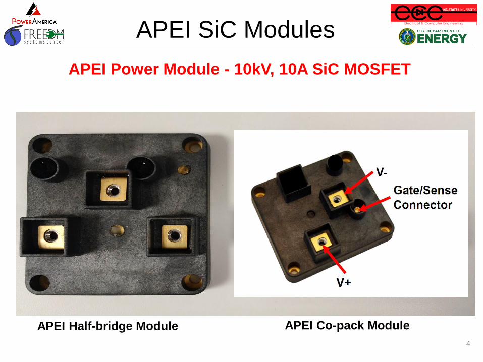
APEI SiC Modules
4
APEI Half-bridge Module APEI Co-pack Module
APEI Power Module - 10kV, 10A SiC MOSFET

10kV SiC MOSFET Co-pack Modules
Single 10kV SiC MOSFET Module
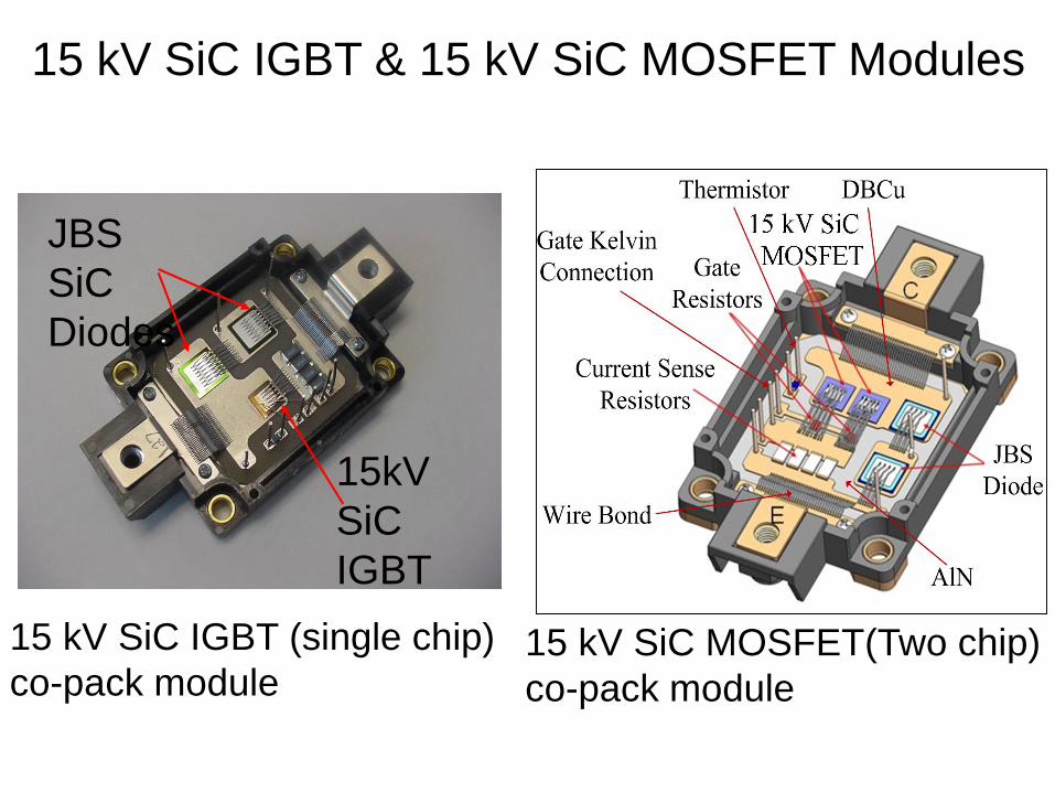
15 kV SiC IGBT & 15 kV SiC MOSFET Modules
15kV
SiC
IGBT
JBS
SiC
Diodes
15 kV SiC IGBT (single chip)
co-pack module15 kV SiC MOSFET(Two chip)
co-pack module
• Provide power and voltage support functions in sub-cycle time scales to keep the grid and embedded Microgridsstable
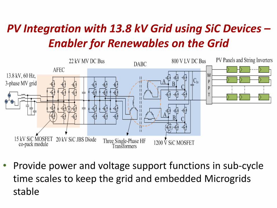
PV Integration with 13.8 kV Grid using SiC Devices –Enabler for Renewables on the Grid
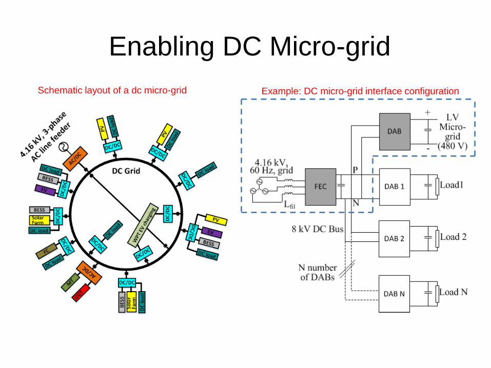
Enabling DC Micro-grid
Schematic layout of a dc micro-grid Example: DC micro-grid interface configuration

9
Transformerless Intelligent Power Substation (TIPS)
• Three-Phase SiC Devices based Solid State alternative to conventional line frequency
transformer for interconnecting 13.8 kV distribution grid with 480 V utility grid.
• Smaller and Light Weight High Frequency Transformer operating at 10 kHz used for Isolation.
• Advantages – Better Power Quality, Controllability, VAR Compensation, Small Size/Light
Weight, lower Cooling Requirement, Integration of Renewable Energy Sources/Storage System
POWER ELECTRONIC
CONVERTERS FOR MEDIUM
VOLTAGE APPLICATIONS
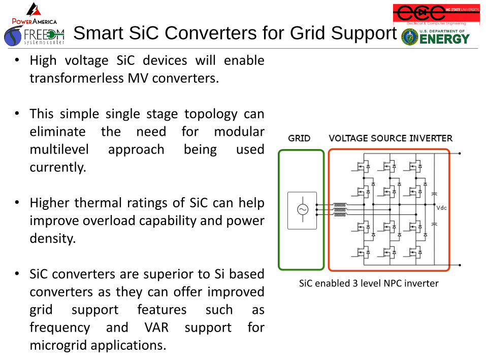
Smart SiC Converters for Grid Support
• High voltage SiC devices will enabletransformerless MV converters.
• This simple single stage topology caneliminate the need for modularmultilevel approach being usedcurrently.
• Higher thermal ratings of SiC can helpimprove overload capability and powerdensity.
• SiC converters are superior to Si basedconverters as they can offer improvedgrid support features such asfrequency and VAR support formicrogrid applications.
SiC enabled 3 level NPC inverter
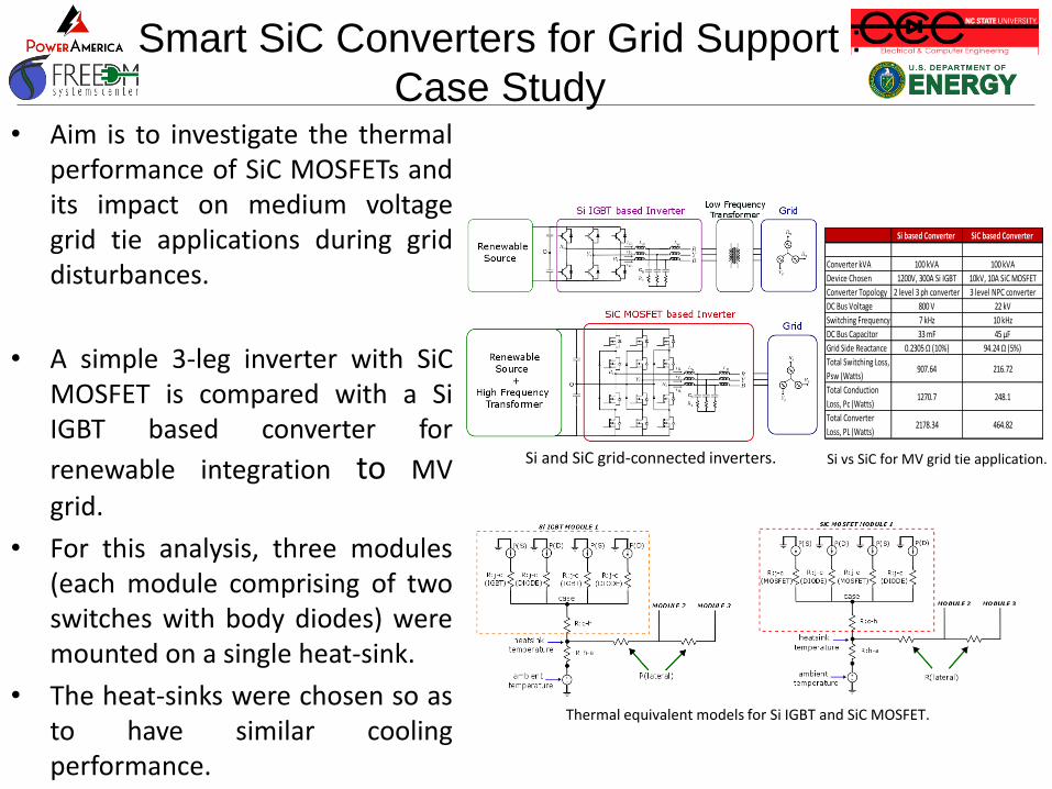
• Aim is to investigate the thermalperformance of SiC MOSFETs andits impact on medium voltagegrid tie applications during griddisturbances.
• A simple 3-leg inverter with SiCMOSFET is compared with a SiIGBT based converter for
renewable integration to MV
grid.
• For this analysis, three modules(each module comprising of twoswitches with body diodes) weremounted on a single heat-sink.
• The heat-sinks were chosen so asto have similar coolingperformance.
Thermal equivalent models for Si IGBT and SiC MOSFET.
Smart SiC Converters for Grid Support :
Case Study
Si based Converter SiC based Converter
Converter kVA 100 kVA 100 kVA
Device Chosen 1200V, 300A Si IGBT 10kV, 10A SiC MOSFET
Converter Topology 2 level 3 ph converter 3 level NPC converter
DC Bus Voltage 800 V 22 kV
Switching Frequency 7 kHz 10 kHz
DC Bus Capacitor 33 mF 45 µF
Grid Side Reactance 0.2305 Ω (10%) 94.24 Ω (5%)
Total Switching Loss,
Psw (Watts)907.64 216.72
Total Conduction
Loss, Pc (Watts)1270.7 248.1
Total Converter
Loss, PL (Watts)2178.34 464.82
Si vs SiC for MV grid tie application.Si and SiC grid-connected inverters.
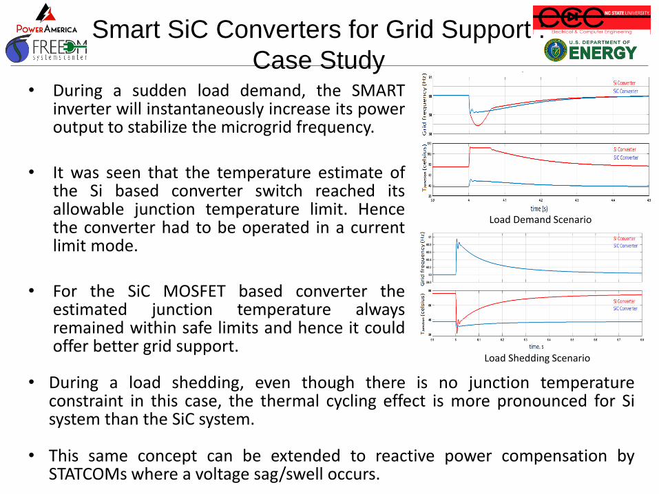
Smart SiC Converters for Grid Support :
Case Study• During a sudden load demand, the SMART
inverter will instantaneously increase its poweroutput to stabilize the microgrid frequency.
• It was seen that the temperature estimate ofthe Si based converter switch reached itsallowable junction temperature limit. Hencethe converter had to be operated in a currentlimit mode.
• For the SiC MOSFET based converter theestimated junction temperature alwaysremained within safe limits and hence it couldoffer better grid support.
Load Demand Scenario
Load Shedding Scenario
• During a load shedding, even though there is no junction temperatureconstraint in this case, the thermal cycling effect is more pronounced for Sisystem than the SiC system.
• This same concept can be extended to reactive power compensation bySTATCOMs where a voltage sag/swell occurs.

Renewable Energy + Battery Energy
Storage System Integration
• TIPS topology is modified to enable renewable integration/distributed energy storage device (DESD).
• Renewable/DESD integration possible at low voltage DC/AC side.
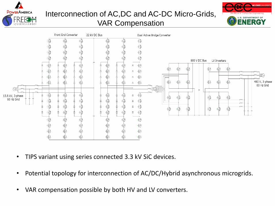
Interconnection of AC,DC and AC-DC Micro-Grids,
VAR Compensation
• TIPS variant using series connected 3.3 kV SiC devices.
• Potential topology for interconnection of AC/DC/Hybrid asynchronous microgrids.
• VAR compensation possible by both HV and LV converters.

16
Intelligent MV (15kV) Isolated Gate Driver
One Gate Driver Photo – Six Used for 3-Phase Converter
• Reduction of coupling capacitance needed for
high dv/dt motor drive applications*
• High voltage insulation requirement for high side
device operation – Kapton Tape used
• Active gate drive can reduce dv/dt**
Specification Value
Turn-on Voltage 20V
Turn-off Voltage -5 V
Supply Input Voltage 9 V
Switching Frequency Up to 20 kHz
Turn-on Gate Resistance 14.7 Ω
Turn-off Gate Resistance 14.7 Ω
Isolation Voltage Up to 15 kV
dv/dt capability > 50 kV/µs
Intelligent MV Gate Driver
Intelligent MV Gate Driver Interface Board

f = 6kHz
VS2gs [20 V/div.]
IS2 [2 A/div.]Vbuck [2 kV/div.]
Vboost [1 kV/div.]
Time Scale [100µs/div.]
Figure: 5 kV boost-buck GD qualification results
Figure: 5 kV boost-buck GD qualification interface side results
f = 6kHz 78 C
zero
meas
Vds(on) [2.7 V/div.]
Vgs [signal]T S1
mod [50 C/div.]
28 C
Time Scale [50µs/div.]
Monitoring test with IMGD Boost-buck
• Boost-buck at 3.75 kW for 30 min - Switching test of 10 kV SiC MOSFET at 5 kV
• Boost input is 1.25 kV and output is 5 kV. The boost duty is 25%
• 30 min thermal run at 5kV and 3.75 kW power
• sp1 pointer near high side IGBT
• Desat-sensing, Vds(on), Tmod and Id are verified
18
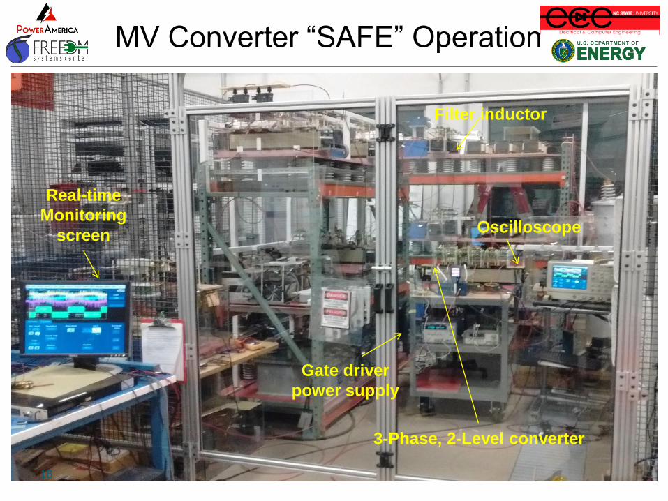
MV Converter “SAFE” Operation
3-Phase, 2-Level converter
Gate driver
power supply
Oscilloscope
Real-time
Monitoring
screen
Filter inductor
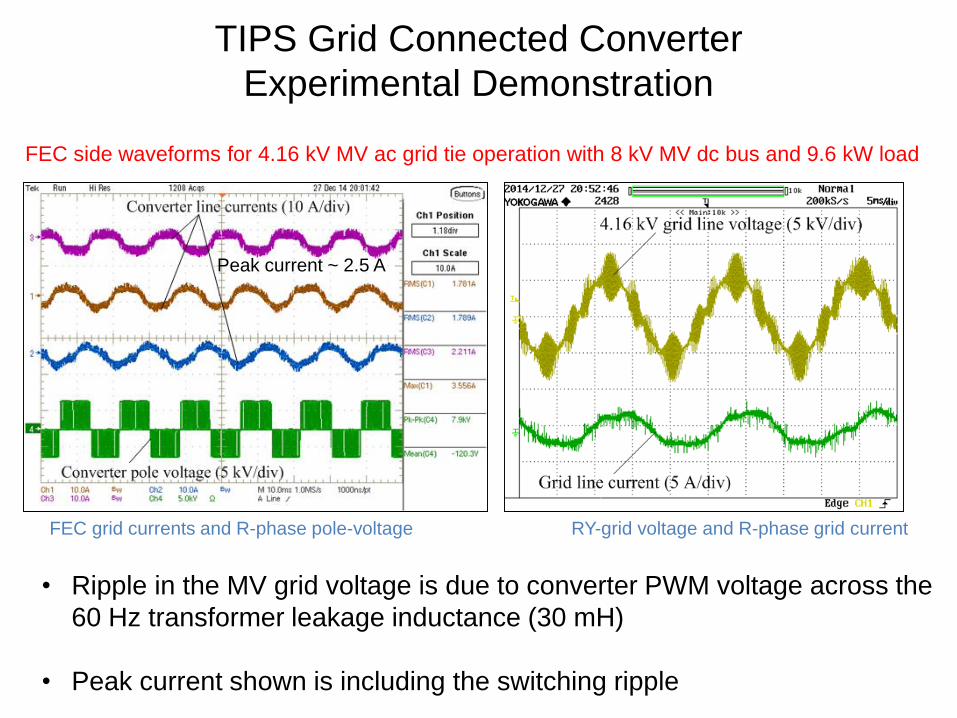
TIPS Grid Connected Converter
Experimental Demonstration
FEC side waveforms for 4.16 kV MV ac grid tie operation with 8 kV MV dc bus and 9.6 kW load
FEC grid currents and R-phase pole-voltage RY-grid voltage and R-phase grid current
• Ripple in the MV grid voltage is due to converter PWM voltage across the
60 Hz transformer leakage inductance (30 mH)
• Peak current shown is including the switching ripple
Peak current ~ 2.5 A
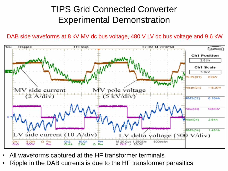
DAB side waveforms at 8 kV MV dc bus voltage, 480 V LV dc bus voltage and 9.6 kW
• All waveforms captured at the HF transformer terminals
• Ripple in the DAB currents is due to the HF transformer parasitics
TIPS Grid Connected Converter
Experimental Demonstration

10kV H-Bridge for 7.2 kV AC grid interface
• No need for complex multilevel
converter topologies
• Simple 2-level VSC control
• Robust 2-level VSC converter
• Compact – size, weight, volume
• Efficient MV power conversion
• Only four 15 kV SiC IGBTs are sufficient for 7.2kV AC single-phase
(7.2kV is single-phase of 3-phase 12.47kV) grid integration, whereas,
at least twelve 6.5 kV Si IGBTs are needed for the same voltage.
• This H-Bridge test showcases the MV power conversion possibilities of
the Cree developed 15kV SiC IGBT device [funded byARPA-E/DOE]
15kV/20A SiC IGBTs

10kV H-Bridge for 7.2 kV AC grid interface
Ch2: AC voltage output (4 kV/div); Ch3: DC Voltage (2 kV/div); Ch4: AC current in R-L load (2 A/div)
10 kV DC bus Voltage Demonstration
The 10kV H-Bridge operated at 10 kV, 5 kHz, 6 kW for 15 mins.
Peak to Peak output ac voltage of 20 kV at 5 kHz PWM switching
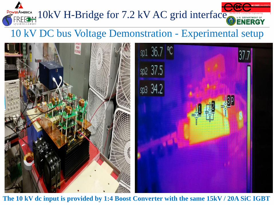
The 10 kV dc input is provided by 1:4 Boost Converter with the same 15kV / 20A SiC IGBT
10kV H-Bridge for 7.2 kV AC grid interface
10 kV DC bus Voltage Demonstration - Experimental setup
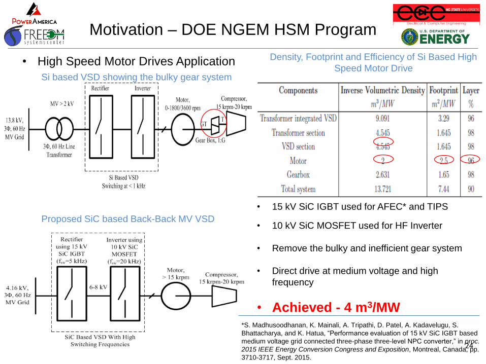
Motivation – DOE NGEM HSM Program
24
• High Speed Motor Drives Application
Si based VSD showing the bulky gear system
Density, Footprint and Efficiency of Si Based High
Speed Motor Drive
Proposed SiC based Back-Back MV VSD
• 15 kV SiC IGBT used for AFEC* and TIPS
• 10 kV SiC MOSFET used for HF Inverter
• Remove the bulky and inefficient gear system
• Direct drive at medium voltage and high
frequency
• Achieved - 4 m3/MW*S. Madhusoodhanan, K. Mainali, A. Tripathi, D. Patel, A. Kadavelugu, S.
Bhattacharya, and K. Hatua, “Performance evaluation of 15 kV SiC IGBT based
medium voltage grid connected three-phase three-level NPC converter,” in proc.
2015 IEEE Energy Conversion Congress and Exposition, Montreal, Canada, pp.
3710-3717, Sept. 2015.
3-Phase, 2-Level Converter
Development and Testing using
10 kV/10 A SiC MOSFETs
25
High Fundamental Frequency
Three-Phase Converter Test
Setup and Results
26
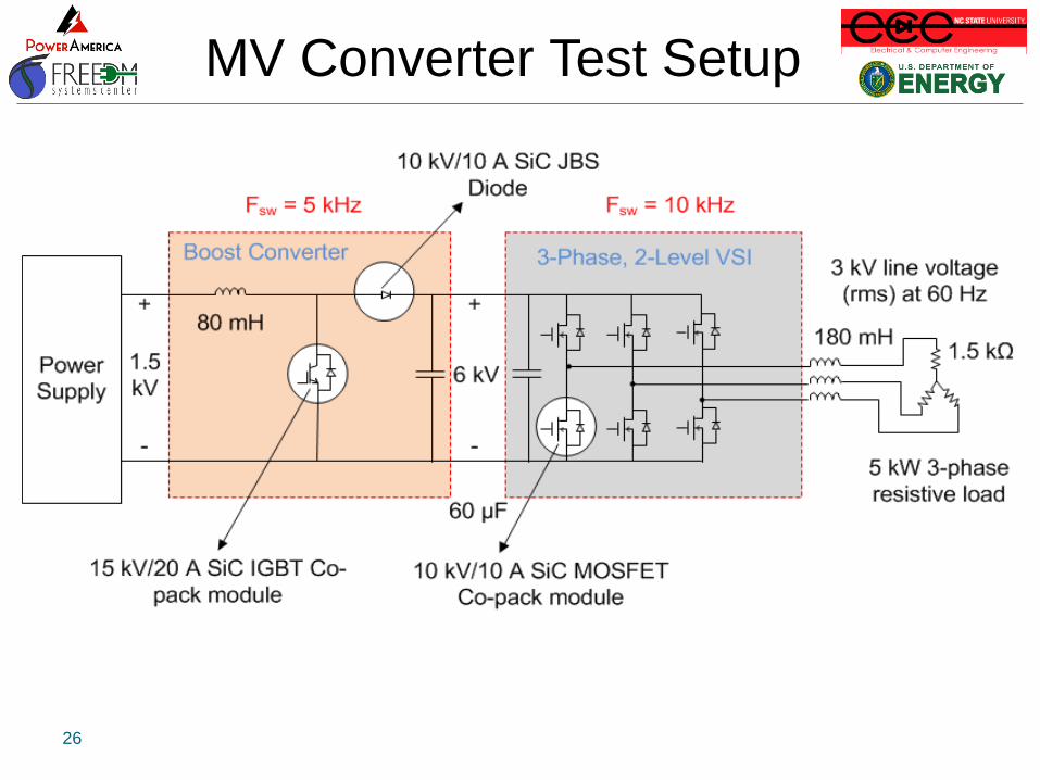
MV Converter Test Setup
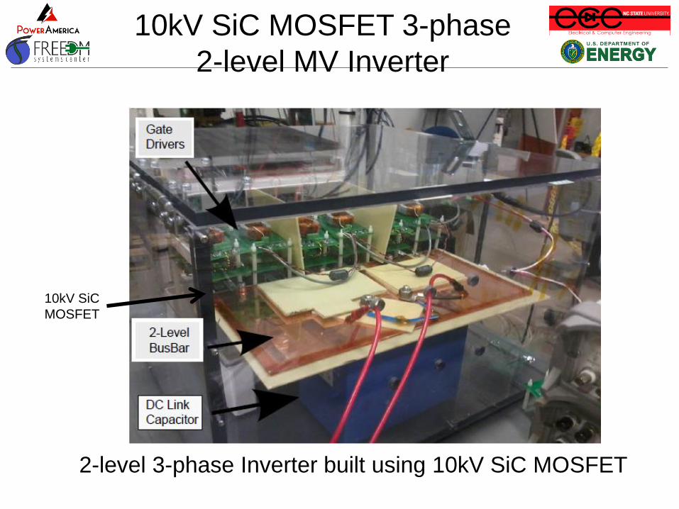
10kV SiC MOSFET 3-phase
2-level MV Inverter
2-level 3-phase Inverter built using 10kV SiC MOSFET
10kV SiC
MOSFET

28
MV Converter Test Setup
Six gate drivers
Six 10 kV/10 A SiC MOSFETS
Cooling Fan
Heat Sinks
with Air
Guide
Pearson current
sensor
CIC Research HV
differential probe
DC bus capacitors
Sandwich bus bar
with FR4 Insulation
All three phase-leg heat sinks
connected together electrically

29
Three-Phase Converter Experimental Waveforms
6 kV DC, 3 kV AC, 5 kW, fsw=10 kHz, fm=60 Hz 5 kV DC, 2.6 kV AC, 3.8 kW, fsw=10 kHz, fm=240 Hz
5 kV DC, 2.6 kV AC, 3.8 kW, fsw=10 kHz, fm=400 Hz
• Up to 400 Hz Fundamental
Frequency with 10 kHz Switching
Frequency
• For Fundamental Frequency Higher
than 400 Hz, Switching Frequency
increased to 20 kHz
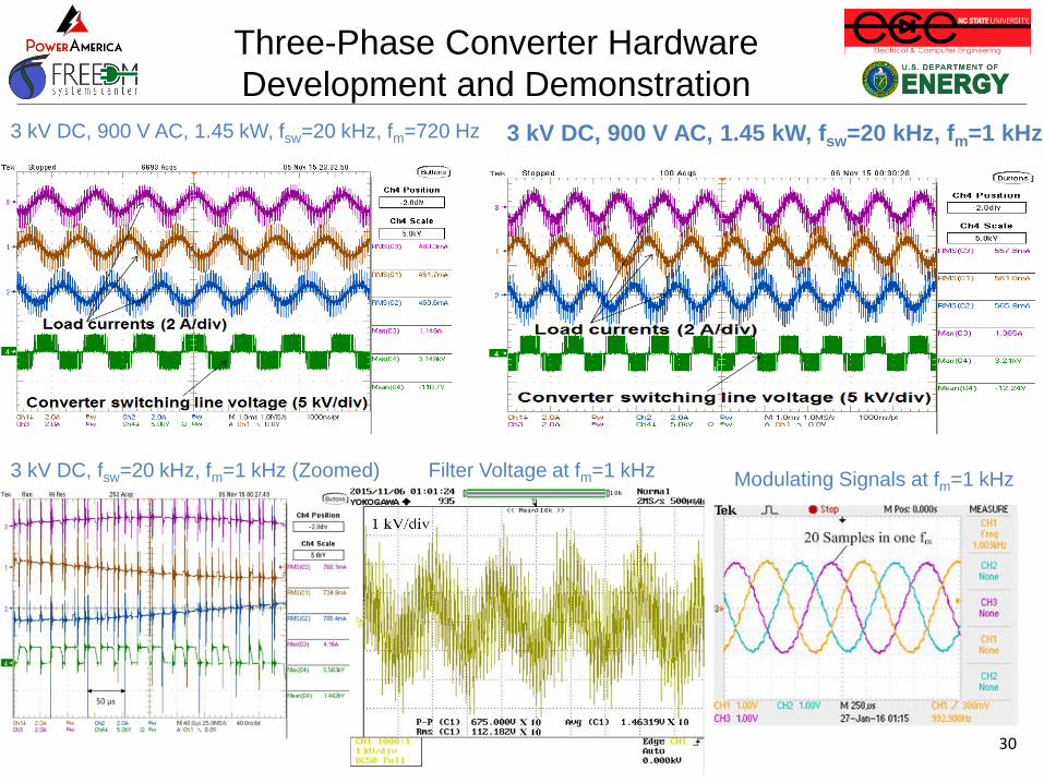
Three-Phase Converter Hardware
Development and Demonstration
30
3 kV DC, 900 V AC, 1.45 kW, fsw=20 kHz, fm=720 Hz 3 kV DC, 900 V AC, 1.45 kW, fsw=20 kHz, fm=1 kHz
3 kV DC, fsw=20 kHz, fm=1 kHz (Zoomed) Filter Voltage at fm=1 kHz Modulating Signals at fm=1 kHz
Three-Phase Converter Hardware
Development and Demonstration

Three-Phase Converter Loss Analysis
31
• PLECS simulation based on real experimental data
Loss Variation with Load at fm = 1 kHz, 6 kV DC, 3 kV AC
• Semiconductor loss
does not vary much
with fundamental
frequency – only 1
kHz considered
• At fsw = 20 kHz and
20 kVA load, total
loss - 695 W
• Efficiency - 96.64%
at a power density of
4.11 W/inch3
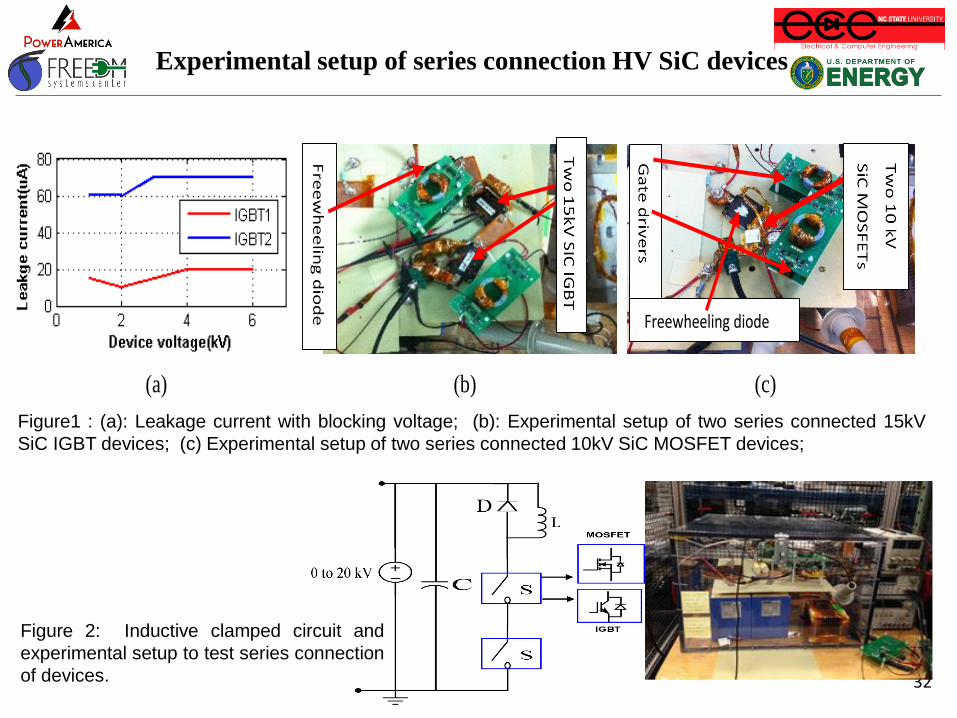
Experimental setup of series connection HV SiC devices
32
(a) (b) (c)
Freewheeling diode
Figure1 : (a): Leakage current with blocking voltage; (b): Experimental setup of two series connected 15kV
SiC IGBT devices; (c) Experimental setup of two series connected 10kV SiC MOSFET devices;
Figure 2: Inductive clamped circuit and
experimental setup to test series connection
of devices.

Experimental results series connection of two
15kV SiC IGBT devices with RC snubber
Figure: Balanced Turn-off characteristics At 10kV DC bus voltage with RC snubber.
[Ch3: Top device VGE (20 V/div); Ch2: Total voltage (1 kV/div); Ch4: Bottom device VCE (1 kV/div);
Math1: Ch2-Ch4: Top device VCE (1 kV/div) Ch1: Bottom device current: IC(5 A/div);]
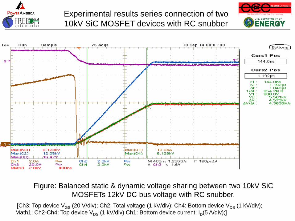
Experimental results series connection of two
10kV SiC MOSFET devices with RC snubber
Figure: Balanced static & dynamic voltage sharing between two 10kV SiC
MOSFETs 12kV DC bus voltage with RC snubber.
[Ch3: Top device VGS (20 V/div); Ch2: Total voltage (1 kV/div); Ch4: Bottom device VDS (1 kV/div);
Math1: Ch2-Ch4: Top device VDS (1 kV/div) Ch1: Bottom device current: ID(5 A/div);]
35
• Comparison of HV switch with
series connected 1.7kV SiC
MOSFETs at 100A and 10kV-
15kV SiC MOSFET modules
(10 parallel connected 10A
modules for 100A)

Outline of LV SiC MOSFET (1.7kV)
Series Connection
36
1. Switching loss comparison of 10kV/100A module (10 parallel connected 10A modules) with series connected LV MOSFET (1.7kV/225A modules) at nearly 5kV/100A switching.
2. Switching loss comparison of 15kV/100A module (10 parallel connected 10A modules) with series connected LV MOSFET (1.7kV/225A modules) at nearly 10 kV/100A switching.
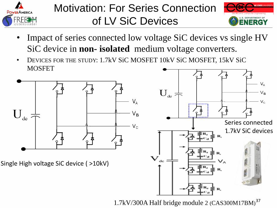
Motivation: For Series Connection
of LV SiC Devices
• Impact of series connected low voltage SiC devices vs single HV
SiC device in non- isolated medium voltage converters.
• DEVICES FOR THE STUDY: 1.7kV SiC MOSFET 10kV SiC MOSFET, 15kV SiC
MOSFET
37
Single High voltage SiC device ( >10kV)
Series connected 1.7kV SiC devices
1.7kV/300A Half bridge module 2 (CAS300M17BM)
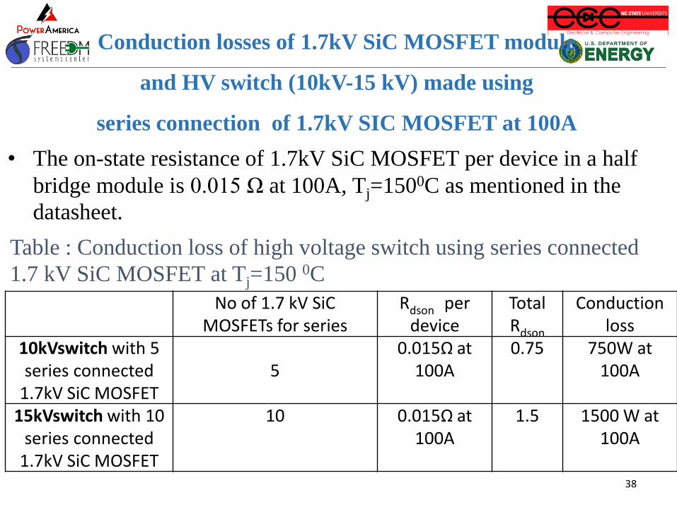
No of 1.7 kV SiC MOSFETs for series
Rdson per device
Total Rdson
Conduction loss
10kVswitch with 5 series connected
1.7kV SiC MOSFET5
0.015Ω at 100A
0.75 750W at 100A
15kVswitch with 10 series connected
1.7kV SiC MOSFET
10 0.015Ω at 100A
1.5 1500 W at 100A
38
Table : Conduction loss of high voltage switch using series connected
1.7 kV SiC MOSFET at Tj=150 0C
Conduction losses of 1.7kV SiC MOSFET module
and HV switch (10kV-15 kV) made using
series connection of 1.7kV SIC MOSFET at 100A
• The on-state resistance of 1.7kV SiC MOSFET per device in a half
bridge module is 0.015 Ω at 100A, Tj=1500C as mentioned in the
datasheet.

Comparison of Switching loss and conduction
losses and dv/dt per HV module
39
Module type, maximum rating
Switching voltage, current
Turn-off dv/dt (kV/µs)
Turn-on dv/dt(kV/µs)
Eoff per module (mJ)
Eon permodule(mJ)
ET = (En+Eoff) per module (mJ)
Rdson at Tj=150 0C
Conduction loss
10kV/10A SiC MOSFET 4.7 kV, 10A 42 20 2.24 11.82
14.06 0.8Ω at 10A
80 W at 10A
15kV/10A SiCMOSFET 10 kV, 10A 32 20 5 47.5
52.5 1.8Ω at 10A
180 W at 10A
Table: Comparison of Switching loss and dv/dt per HV module

Comparison of total losses of HV SiC module and HV switch with series
connected LV SiC MOSFETs
• For 100A operation, it has been assumed that the ten number of HV
modules connected in parallel of 10kV/10A and 15kV/10A devices
respectively.
• The thermal resistances of module (Rthj-c) of 15kV, 20A SiC IGBT (with
single IGBT chip) 0.650C/W[1]. 10kV/15kV SiC MOSFET has same
packaging of that 15kV SiC IGBT, so it has been assumed same thermal
resistance .Therefore, the effective thermal resistance with ten parallel
devices of 10kV module will be 0.0650C/W and of 15 kV module will be
0.03580C/W ( because each module has two parallel chips).
• The thermal resistance of 1.7kV SiC MOSFET device is 0.0710C/W.
Therefore, the effective thermal resistance with five, ten series
connected devices will be 0.00140C/W and 0.0070C/W respectively for
making 5kV, 10kV HV series switch.
40
1. Kasunaidu Vechalapu, et al.,” Comparative Evaluation of 15 kV SiC MOSFET and 15 kV SiC IGBT for Medium
Voltage Converter under Same dv/dt Conditions”, Energy Conversion Congress and Exposition (ECCE), 2015 IEEE.
@ Copyright 2016 by Kasunaidu Vechalapu
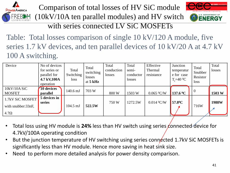
Comparison of total losses of HV SiC module
(10kV/10A ten parallel modules) and HV switch
with series connected LV SiC MOSFETs
Device No of devices
for series or
parallel for
4.7 kV,100A
operation
Total
Switching
loss
Total
switching
losses
at 5 kHz
Total
conduction
losses
Total
semi-
conductor
losses
Effective
Thermal
resistance
Junction
temperatur
e for case
Tc=40 0C
Total
Snubber
Resistor
loss
Total
losses
10kV/10A SiC
MOSFET
10 devices
parallel140.6 mJ 703 W
800 W 1503 W 0.065 0C/W 137.6 0C0
1503 W
1.7kV SiC MOSFET
with snubber:33nF,
4.7Ω
5 devices in
series104.5 mJ 522.5W
750 W 1272.5W 0.014 0C/W 57.80C716W
1988W
41
Table: Total losses comparison of single 10 kV/120 A module, five
series 1.7 kV devices, and ten parallel devices of 10 kV/20 A at 4.7 kV
100 A switching.
• Total loss using HV module is 24% less than HV switch using series connected device for 4.7kV/100A operating condition
• But the junction temperature of HV switching using series connected 1.7kV SiC MOSFETs is significantly less than HV module. Hence more saving in heat sink size.
• Need to perform more detailed analysis for power density comparison.

42
Device No of
devices for
series or
parallel for
10kV,100A
operation
Total
Switching
loss
Total
switching
power
losses
at 5 kHz
Total
conduction
losses
Total semi-
conductor
losses
Effective
Thermal
resistance of
module
(Rthj-c)
Junction
temperatureTotal
Snubber
Resistor
loss
Total
losses
15kV/20A SiC
MOSFET10 devices
in parallel525 mJ 2625 W 1800 W 4425 W
0.0358 0C/W
158 0C 0 4425 W
1.7kV SiC
MOSFET with
33nF, 4.7Ω
10 device
in Series209 mJ 1045 W 1500 W 2545 W 0.007 0C/W 57.80C 1432 W 3977 W
Table :Total losses comparison of ten series 1.7 kV devices, and ten parallel devices of 15
kV/20 A at 10 kV 100 A switching.
• For 10 kV, 100A operation, HV switch with series connected 1.7kV SiC MOSFETs has
lower total loss (10 % less) compared to 15kV HV SiC MOSFET for one of the snubber
value.
• Also the junction temperature of HV switching using series connected 1.7kV SIC MOSFETs
is significantly less than HV module. Hence more saving in heat sink size.
• Therefore the breakeven point for HV SiC MOSFET module more efficient could be around
10kV to 12kV beyond that series connection LV SiC MOSFET is more favorable for high
voltage bus.
Comparison of total losses of HV SiC
module(single or parallel) and HV switch
with series connected LV SiC MOSFETs
43
Acknowledgement
• This work is supported by US Govt. through the DOE NNMII Power America Institute
• This work made use of FREEDM ERC shared facilities supported by National Science
Foundation under award no. EEC-0812121.
Thank You!!!
Questions
Acknowledgements: FREEDM Systems Center, PowerAmerica
ARPA-E and DOEDept. of ECE, NC State University