copyright © 1979, by the author(s). all rights reserved
TRANSCRIPT

Copyright © 1979, by the author(s). All rights reserved.
Permission to make digital or hard copies of all or part of this work for personal or
classroom use is granted without fee provided that copies are not made or distributed for profit or commercial advantage and that copies bear this notice and the full citation
on the first page. To copy otherwise, to republish, to post on servers or to redistribute to lists, requires prior specific permission.

MOS SWITCHED CAPACITOR LADDER FILTERS
by
David James Allstot
Memorandum No. UCB/ERL M79/30
May 1979
f /•••> Vi )
l'MOS SWITCHED CAPACITOR LADDER FILTERS
t by
(V
David James Allstot
Memorandum No. UCB/ERL M79/30
May 1979
ELECTRONICS RESEARCH LABORATORY
College of EngineeringUniversity of California, Berkeley
94720

Ph.D.
MOS SWITCHED CAPACITOR LADDER KILTERS
Duvid James Allstot Dept. of ElectricalEngineering andComputer Sciences
Chairman of Committee /r
ABSTRACT
Switched capacitor techniques have been investigated for realizing preci
sion high-order, frequency-selective filters using standard MOS technology.
New techniques have been developed for designing recursive switched capacitor
singly- and doubly-terminated active ladder filters which simulate low-
sensitivity passive RLC ladder networks.
Three fully-integrated experimental NMOS prototypes have been designed
and fabricated. The first circuit implemented a fifth-order Chebyshev lowpass
response with 0.1 dB passband ripple and an 83 dB dynamic range. The second
design was a third-order Elliptic lowpass filter which verified a new and efficient
method of including complex transmission zeros. This filter achieved a 90 dB
dynamic range with a power dissipation of 18 mW. The third design was an
electrically-programmable second-order switched capacitor section with lowpass.
bandpass, and bandreject outputs. This filter demonstrated a new technique
for programming a filter response using weighted capacitorarrays.
In the switched capacitor technique, MOS capacitor ratios and sampling
frequency are used as the precision elements. MOS operational amplifiers with
moderate performance specifications are used to implement the switched capa
citor integrators.
* %»
ACKNOWLEDGEMENTS
I am very grateful to Professors Robert W. Brodersen, Paul R. Gray, and
David A. Hodges for the opportunity to participate in their MOS analog circuit tech
niques research program. Their technical guidance and assistance are largely
responsible for the success of this project. I have also benefitted greatly from the
personal advice, encouragement, and support from my closest advisors.
Professors Paul R. Gray, and Robert W. Brodersen. I am indebted to many of the
graduate students in the Integrated Circuits Group, both past and present, for their
useful discussions and assistance.
The laboratory assistance of D. McDaniel and D. Rogers is acknowledged, and
the efforts of D. Simpson, C. Tast, B. Fuller and B. Kerekes are appreciated.
The measurement assistance provided by the Hughes Aircraft Corp., and the
die photography provided by Texas Instruments, Inc., areacknowledged.
This research was supported by the Joint Services Electronics Program Con
tract F44620-76-C-0100, by the Naval Research Office Contract N000173-77-C-
0238, and by a doctoral fellowship from the IBM Corporation.

u
DEDICATION
My wife, Vickie, meticulously drew most of the thesis figures and was a great
help in assembling the final draft. Without her love, understanding and encourage
ment, none of this work would have been possible.
I dedicate this thesis to her for the many sacrifices she has made.
ill
TABLE OF CONTENTS
CHAPTER 1: INTRODUCTION 1
CHAPTER 2: SWITCHED CAPACITOR LADDER FILTER SYNTHESIS.. 62.1. Sensitivity of the Doubly-Terminated RLC Ladder Filter 62.2. The MOS Switched Capacitor Resistor Concept 92.3. The MOS Switched Capacitor Integrator 142.4. Flowgraph Synthesis Techniques 182.5. MOS Switched Capacitor Filter Circuits 22
2.5.1. Doubly-Terminated All-Pole Lowpass Ladder Filter 222.5.2. Lowpass Ladder Filter with Finite Transmission Zeros 252.5.3. Singly-Terminated All-Pole Lowpass Ladder Filter 302.5.4. Doubly-Terminated Bandpass Ladder Filters 302.5.5. Singly-Terminated Bandpass Ladder Filter 362.5.6. Singly-Terminated Highpass Ladder Filter 362.5.7. Doubly-Terminated Highpass Ladder Filter 442.C.8. Doubly-Terminated Elliptic Highpass Ladder Filter 48
CHAPTER 3: CONSIDERATIONS FOR THEMONOLITHIC MOS IMPLEMENTATIONOF SWITCHED CAPACITOR FILTERS 53
3.1.Sampled-Data Discrete-Time Effects 533.1.1. Continuous-Time RC Integrators 533.1.2. Discrete-Time Switched Capacitor Integrators 553.1.3. DDI SwitchedCapacitor Filters without Predistortion 603.1.4. DDI Switched Capacitor Filters with Predistortion 663.1.5. Type-1 LDI Switched Capacitor Filters 693.1.6.Type-II LDI Switched Capacitor Fillers 753.1.7. LDI SwitchedCapacitor Filters with Predistortion 813.1.8. SwitchedCapacitor Filters with MultipleSampling Rates 82
3.2. Passive Component Nonideal Effects 823.2.1. MOSFET Channel (Switch) Resistance 863.2.2. MOSFET Nonlinearity and Threshold Voltage Effects 873.2.3. MOSFET Channel-Resistance Thermal Noise 893.2.4. Capacitively-Coupled Clock Feedthrough 893.2.5. Junction and Surface Leakage Currents 893.2.6. MOS Capacitor Ratio Errors 923.2.7. MOS Capacitor Temperature Coefficient 933.2.8. MOS Capacitor Voltage Coefficient 933.2.9. Parasitic Capacitances 94
iv
3.3. Nonidealities Associated with the Active Components 963:3.1. Operational Amplifier DC Open-Loop Gain 963.3.2. Operational Amplifier DC Offset Voltage 973.3.3. Common-Mode Range and CMRR 993.3.4. Amplifier Slew-Rate 993.3.5. Amplifier Settling Response 100
CHAPTER 4: DYNAMIC RANGE CONSIDERATIONSFOR SWITCHED CAPACITOR FILTERS 105
4.1. Harmonic Distortion in a Switched Capacitor Integrator 1064.2. Scaling Techniques for Switched Capacitor Filters Ill
4.2.1. Impedance Scaling 1114.2.2. Switched Capacitor Node-Voltage Scaling 1154.2.3. Switched Capacitor Loop Scaling 118
4.3. Noise in a Switched Capacitor Integrator 123
CHAPTER 5: EXPERIMENTAL RESULTS
FOR NMOS LOWPASS PROTOTYPES 1335.1. NMOS Depletion-Load Operational Amplifier 133
5.1.1. DC Open-Loop Gain 1335.1.2. Equivalent Input Offset Voltage 1385.1.3. Common-Mode Range and CMRR 1385.1.4. Equivalent Input Noise 1385.1.5. Power Supply Rejection 1425.1.6. Power Supply Current versus SupplyVoltage 1425.1.7. Slew-Rate Performance 1425.1.8. Unity-Gain Bandwidth 142
5.2. DDI Switched Capacitor Fifth-Order Chebyshev Lowpass Filter 1425.2.1. Frequency Response 1475.2.2. Frequency Response versus Sampling Rate 1475.2.3. Frequency Response versus Power Supply Variations 1525.2.4. Harmonic Distortion 1525.2.5. Noise Performance 152
5.3. LDI Switched Capacitor Third-Order Elliptic Lowpass Filter 1575.3.1. Frequency Response 1575.3.2. Frequency Response versus Sampling Rate 1625.3.3. Frequency Response versus Power Supply Voltages 1625.3.4. Harmonic Distortion 1625.3.5. Noise Performance 1695.3.6. Power Supply Rejection 1695.3.7. Phase Sensitivity 1695.3.8. Temperature Performance 1695.3.9. Intermodulation Distortion 1695.3.10. Quantizing Noise 175
CHAPTER 6: AN ELECTRICALLY-PROGRAMMABLESWITCHED CAPACITOR FILTER 177
6.1. Synthesis of the Programmable Second-Order Section 1776.2. Design of the Programmable Switched Capacitor Arrays 1806.3. Practical Design Considerations ]g6
6.3.1. Sampled-Data Transfer Functions 1866.3.2. Exaci Design Equations igg6.3.3. Op Amp DC Gain Effects for Integrator Stages 1886.3.4. Op Amp Gain Effects for Bandreject Stage 1906.3.5. Top-Plate Parasitic Capacitance 193
6.4. NMOS Prototype Experimental Results 1946.4.1. Center Frequency Programming 1956.4.2. Clock Frequency Programming 1956.4.3. Selectivity Programming J9g6.4.4. Gain Programming 1956.4.5. Low-Q Passband Details 1936.4.6. Dynamic Range 195
6.5. A Formant Speech Synthesis System 2026.5.1. The Vocal Tract Model 2026.5.2. ASwitched Capacitor Formant Synthesizer 204
CHAPTER 7: CONCLUSIONS 207
APPENDIX 1: NMOS METAL-GATE
ENHANCEMENT-DEPLETION PROCESS 209
APPENDIX 2: NMOS ENHANCEMENT-DEPLETIONDEVICE CHARACTERISTICS 214
APPENDIX 3: SIMULATION TECHNIQUESFORSWITCHED CAPACITOR FILTERS 217
REFERENCES 225

Chapter 1
INTRODUCTION
Precision high-order filters are widely used in various types of electronic equip
ment such as telecommunications and other voice-band systems 111. Monolithic
implementation of these low frequency filters requires the realization of long time
constants in small silicon area, and the realization of transfer functions that are
insensitive to parameter variations. In addition, it is desirable to obtain a very pre
cise response without external trimming operations. Conventional active filters
implemented with thin-film or hybrid technologies do not meet these requirements,
and thereforeare not suitable for many applications.
Recently, these objectives have been realized in a monolithic implementation
using acompatible Bipolar/JFET technology [21. Although excellent results have
been obtained, this approach requires arelatively large chip area for low frequency
applications, and the required bipolar process is not directly compatible with dense
digital logic which is needed for many LSI system applications.
Another promising monolithic filtering approach uses charge transfer devices
(CTD's) to implement sampled-data transversal filters 13]. In the past, this
approach had two main disadvantages: (1) The large inserUon loss (which was typi
cally 20 dB) limited the available dynamic range [41, and (2) the relatively low sam
pling rates complicated the design of the continuous-time anti-alias prefilter [5]. Ifhigher clock frequencies were used relative to the passband frequencies in order to
reduce the prefilter requirements, more CTD stages were required which further
reduced the dynamic range and increased the silicon area requirements. Recently,
these problems have been solved by using adouble split-electrode CCD structure
operating at 32 kHz with a 128 kHz sampled-data prefilter [441. This approach
appears to be very promising for future applications.
In the 1960's and early 1970's, filtering by using switches and capacitors was
investigated theoretically [6]-[81. At that time, a suitable integrated circuit technol
ogy did not exist which could efficiently realize these filters. Recent work using
analog sampled-data techniques has demonstrated the viability of MOS technology
for implementing second-order filters. The classical direct-form second-order digital
filter section [91-[101 has been implemented in an equivalent integrated circuit form
using an MOS sampled-data approach [11]. This approach (as well as the direct-
form digital prototype) has a relatively high sensitivity of the transfer function to
component variation with the additional disadvantage that the sensitivity increases
as the ratio of the sampling rate to passband frequencies increases. Hence, there is
a tradeoff between the sensitivity properties of the direct-form sampled-data filter,
and the requirements for the continuous-time anti-aliasing prefilter.
In digital filter implementations, these problems were solved by using a
modified second-order structure [121. Recently, MOS equivalents of these filters,
as well as biquad second-order sections, have been realized with excellent results
using switched capacitors to simulate resistors in sampled-data switched capacitor
integrator configurations [13]-[15]. A major advantage of this approach is that the
sensitivity of the response of these filters decreases with increasing clock frequency,
in contrast to the direct-form implementations. Unfortunately, high-order filters
realized by cascading these second-order sections can be too sensitive to component
variations to meet high-precision filtering requirements.
It is well known from modern filter theory that for high-order fillers, a passive
doubly-terminated RLC ladder achieves very low sensitivity to component varia
tions in the passband response, and in fact, has zero sensitivity when the power
transfer is maximized between source and load [161-117). This low sensitivity is
maintained by using "leapfrog" or "active ladder synthesis" to simulate RLC ladder
networks with active filter building blocks (181-120). In order to obtain minimum

sensitivity high-order filters, a similar approach to the leapfrog design was taken in
this thesis which makes use of new switched capacitor techniques. The precision
elements in these filters are monolithic MOS capacitors whose ratios determine the
frequency response. The inherent temperature stability (< 25 ppm/°C) and high
matching accuracy (0.1%) of MOS capacitor ratios [21]-[23l make it possible to
implement monolithic high-order filters with extremely precise frequency
characteristics 124]-(251.
The approach to synthesis taken in this dissertation will be to configure the
switched capacitor circuits to simulate the low-sensitivity continuous-time RLC
ladder circuits, so that the design tables that are available for these fillers can be
used [26M271. It will be shown that it is possible to minimize most of the
discrete-time effects (particularly phase shifts due to time delays) which will allow
design using classical continuous-time theory directly. However, one discrete-time
characteristic which must be considered is the necessity of providing a continuous-
time anti-aliasing prefilter preceding the switched capacitor filter. The low sensi
tivity properties of the ladder filters are actually improved with increased sampling
frequency, and thus, the anti-aliasing prefilter requirements are greatly reduced
(compared to theCTD and direct-form approaches) by operating the switched capa
citor filters at clock frequencies which are many limes greater than the passband
frequencies.
InChapter 2, the sensitivity properties of doubly-terminated RLC ladder filters
are presented. The signal flowgraph synthesis procedure is reviewed, and various
filter types are synthesized using switched capacitor integrators as the basic building
blocks. Several new singly- and doubly-terminated highpass structures are
presented.
In Chapter 3, the practical design aspects for MOS integrated circuit implemen
tations of switched capacitor ladder filters are given along with a description of the
effects of finite sampling frequency. A new LDI integrator is presented which is
insensitive to parasitic capacitance.
In Chapter 4, noise and dynamic range considerations for MOS active ladder
filters are presented. Also presented are new scaling techniques which are more
general than the scaling procedures which are used in the RLC prototypes.
In Chapter 5, experimental results obtained from two different integrated
NMOS switched capacitor ladder filters are described. The first design is a Che
byshev fifth-order all-pole lowpass filter, and the second design implements a
third-order elliptic lowpass response including a very efficient realization of
transmission zeros. These filters achieve very precise responses with wide dynamic
range while requiring small chip area, low power dissipation, and relatively low per
formance operational amplifiers. An NMOS depletion-load operational amplifier
design is also summarized.
Chapter 6 presents the synthesis procedures and design considerations for an
MOS switched capacitor programmable filter for applications in formant speech syn
thesis. New experimentaKresults are presented for a programmable second-order
switched capacitor section.
A summary of this research project is presented in Chapter7.
In Appendix 1, the NMOS depletion-load metal-gate process which was used
to fabricate the experimental test circuits is given.
Appendix 2 contains the measured NMOS device parameters which are used
to estimate the performance parameters for the NMOS operational amplifier.
In Appendix 3, models are presented which are useful for simulatingswitched
capacitor filters using a digital network analysis program called D1NAP [28]. It is
shown that most of the important analog effects can be modelled in the digital
domain. This approach has the advantage of accurately predicting discrete-time

effects in contrast to a continuous-time simulation approach.Chapter 2
SWITCHED CAPACITOR LADDER FILTER SYNTHESIS
This chapter begins with a review of the sensitivity properties of doubly-
terminated RLC ladder filters followed by a review of the switched capacitor resis
tor concept, and the development of the switched capacitor integrator. In the final
sections, the signal flowgraph synthesis procedure is developed and used to design
both singly- and doubly-terminated lowpass, bandpass, and highpass switched capa
citor ladder fillers.
2.1. Sensitivity of the Doubly-Terminated RLC Ladder Filter
For high-order filters, a passive doubly-terminated RLC ladder achieves very
low sensitivity in the passband response, and in fact, has zero sensitivity when the
power transfer is maximized between source and load |16]-(17). Fig. 2.1(a) shows
a doubly-terminated RLC fifth-order lowpass ladder filter. In Fig. 2.1(b), the power
delivered to the output is plotted for variation of a component value. When all ele
ments achieve their nominal values, the power delivered to the output is max
imum. However, if a reactive element value is either increased or decreased, the
dPpower delivered to the output decreases. Since the slope, ——, is nominally zero,
oX
small perturbations in the element values will cause very small changes in the
passband response of the filter [27].
The low passband sensitivity is illustrated by considering a specific example.
The fifth-order RLC lowpass ladder filter of Fig. 2.1(a) has been frequency scaled
to realize a Chebyshev response with 0.1 dB nominal passband ripple and a nominal
cutoff frequency of 3.4 kHz as shown in Fig. 2.2(a) [291. The transfer function of
this particular filter is most sensitive to the variation of C3. Fib. 2.2(b) shows the
simulated results for the passband deviation from the nominal design for ±1%

R1 L-2 L4
IN Ci^TVi c :tv5 R2ffV6 VOUTs^r
"ii VI, vl,
(a)
= 0NOM
MAX
^X
(b)NOM
Fig. 2.1. (a) An RLC doubly-terminated fifth-order lowpass ladder filter;(b) the output power for variation of a reactive element value. Fig. 2.2. (a) A nominal fifth-order Chebyshev lowpass response with 0.1 dB
passband ripple and a 3.4 kHz cutoff frequency; (b) simulatedpassband deviation for ±1% variations in C3.

variations in C3 (30J. At those frequencies where the filter response of Fig. 2.2(a)
has again of -6dB, indicating maximum power transfer, the passband deviation,and hence the sensitivity of Fig. 2.2(b) is zero. The sensitivity across the entire
passband is very low since a variation of ±1% in C3 results in a maximum
passband deviation of only ±0.015 dB. The passband sensitivity of this doubly-
terminated RLC ladder is about 10 times lower than a similar singly-terminated
RLC ladder [31], and about 20 times lower than a similar cascade RLC realiza
tion [321. Hence, for implementing high-order, high precision monolithic filters, itis desirable to use an equivalent form of the doubly-terminated RLC structure in
order to obtain the desired low sensitivity. Unfortunately, the network of
Fig. 2.1(a) contains both inductors and resistors which are difficult to implement in
MOS technology. The next sections will describe an approach for converting an
RLC filter into an equivalent MOS switched capacitor ladder which is well-suited for
integration, and which retains nearly ideal sensitivity properties.
2.2. The MOS Switched Capacitor Resistor Concept
Large resistance values are difficult to accurately realize in integrated circuits
due to the lack of high resistivity regions. One possible solution to this problem is
to use lightly doped polysilicon resistors. Unfortunately, the absolute values of
these resistors vary widely with temperature and processing variations, and their
voltage coefficient is rather large 133). Ion implanted and diffused resistors have
similar disadvantages as shown in Table I [34]. (These resistors are often adequatefor the required continuous-time anti-aliasing prefilter).
Recently, these disadvantages have been overcome by using acapacitor which
is switched between voltage sources to simulate a resistor as shown in
Fig. 2.3(b) [13J-I151. At time t, *, turns on MOSFET MA, and Cu is charged to
OLTAGE:fficient
bo
>
Ea
.
bo
>
EQ
. Q.
bo
>
Ea
. a. >
Soo
oo
oo<N CM
1C
O
1
LU
m- 3ZO °,s
(TO
oo
E
o
Ea
.
oO-«.
o £6^rti.
a.
a.
a.
o.
a.
o OCL 51LUUJO
IS) CM
oin
ooino
'—c^" >* + +
.,_,^ :hingracys5^ °*
UDO
—E M
—Ol3i3§ MATC
ACCU
o•»-•II O_J
o d
tr. cc c>L
Uo i- Q
_cc t- i/iQ
>-
o l/>L
U
h-
1-•—
i/iH
to LUZ«K oLU
QC
Q.
CO
1-
ZL
U<
CC
aZ
o
Zo LU
aZc:ot/> -
j~LU
a.
l/> 3cc zo
3:
o ti</>
o2 ll.>
:o
1a_
i
oa
.
Table I. Properties of monolithic resistors and capacitors.
10

V ON
V,OFF
V,ON
V,OFF
Vi
V,
R-VWV——^o V2
I
(a)
(b)
(c)
*1
<t>:
Fig. 2.3. (a) A conventional resistor, and (b) a switched capacitor "resistor";(c) the two-phase non-overlapping clock signals used to switch theMOSFET's.
11 12
Qi - CUV, (2.1)
At time (t + Tc), <t>2 turns on MOSFET MB (MA is now turned off), and Cu is
charged to
Q2 - cuv2.
The current which flows onto Cu is given by
. A£ QCVa-V,)At Tc
(2.2)
(2.3)
The current flowing through the resistor of Fig. 2.3(a) during the same period of
time is
IVa-V,
(2.4)
Therefore, an equivalent switched capacitor resistance, Req, can be defined by
equating Eqns. (2.3) and (2.4):
R «i--L_ (2.5)
where Cu is the switched capacitor value, and fc is the sampling frequency. This
equivalence is valid for sampling rates which are much greater than the signal fre
quencies of interest. If this condition is not met, more exact sampled-data analysis
is required [35]-[36].
Cu may be switched between two points which are not voltage sources. For
example, in Fig. 2.4, the resistor, R,, is replaced by the switched capacitor, C,, to
form a sampled-data passive lowpass filter. Sampled-data techniques are required to
analyze these circuits, and in certain cases, other factors such as clock duty cycles

R
JVAAAr
V,N C2^rs Vqut
00
(b)
Fig. 2.4. (a) A single-pole RC lowpass filter, and (b) a passive single-poleswitched capacitor lowpass filter.
• •. * •
13 14
must be considered which can greatly complicate the design [37]. In this disserta
tion, it will be assumed that the switching occurs between voltage sources (includ
ing virtual grounds) as in the example of the switched capacitor integrator which
will be described in the next section.
2.3. The MOS Switched Capacitor Integrator
Conventional filtering approaches used to implement audio and other low fre
quency filters would require RC integrators, as in Fig. 2.5(a), with long time con-
! slants. If the time constants were realized as RC products, large amounts of chip
area would be required. Another disadvantage of this approach is that in order to
insure reproducibility, the absolute values of both R and C must be tightly con
trolled, which is extremely difficult for typical temperature and processing variations
as indicated previously in Table 1.
These disadvantages are overcome by using the switched capacitor circuit
j shown in Fig. 2.5(b) which, when the ratio of the sampling frequency to the max-
' imum passband frequency is large, closely approximates the conventional integrator
of Fig. 2.5(a) [13]-[14]. The switched capacitor integrator is operated with two-
phase nonoverlapping clocks as shown earlier in Fig. 2.3(c). During the sample
phase, 0|, the switches are thrown to the left, and the difference between voltages
V, and V2 is sampled and stored on Cu. During the integration phase, <f>2, the
switches are thrown to the right, and the difference voltage is scaled and stored on
C|. By switchingCu at a high clock rate, fc, relative to the passband frequencies, an
equivalent resistance is obtained of value
lEQ1
fc<V
I resulting in an integrator gain constant of
(2.6)

-oV0UT
oVquT
Fig. 2.5. (a) A conventional RC differential integrator, and (b) a switchedcapacitor integrator with differential inputs.
1516
REqC fe c,(2.7)
Fig. 2.5(b) can also be analyzed directly using a z-domain analysis [35], and
the conservation of charge principle. Assuming ideal components, the charge
stored on the capacitors at time (t-Tc) is
q,(t-Tc) - Cu[v2(t-Tc)-V,(t-Tc)] (2.8a)
and
q2(t-Tc) - C,V0Ul(t-Tc). (2.8b)
At time t when the switches are thrown to the right, the op amp discharges Cu onto
C], and the system charge is now
q2(t) - C,V0Ul(t) (2.9a)
and
q,(t) - 0. (2.9b)
Eqns. (2.8) and (2.9) can be equated to yield
V0UI(t) - -^ [v2(t-Tc)-V,(t-Tc)] +Voul(t-Tc). (2.10)
In the z-domain, this expression becomes
Vou,(z) |z-,V2(z)-z-,V,(z)] +z-»Vout(z) (2.11)
which is solved for Voul(z):

17
VOUI(z)l-z->
(2.12)
Assuming f«fc, and replacing z=esTc in Eqn. (2.12) by its Taylor series expansion,
fcVoul(s) « [v2(s)-V,(s)j, (2.13)
with s=e$ c. Hence, the term "integrator" is used to represent this building block,
and the gain constant derived from Eqn. (2.13) agrees with the intuitive result of
Eqn. (2.7). The differential integration property isalso evident from Eqn. (2.12).
The switched capacitor realizes very large resistance values in very small chip
areas. For example, from Eqn. (2.5), it is seen that by switching a 1 pFcapacitor at
100 kHz, an equivalent resistance of 10 Mfl is realized in an area of only about
5mil2 for Cu plus a few additional mil2 for the two minimum geometry MOSFET
switch transistors. (It is also interesting to note from Eqn. (2.5) that as the resis
tance value increases, the area required for its switched capacitor implementation
actually decreases). If this equivalent resistor is used in conjunction with C|«=10CU,
again constant of 104 radians/sec is obtained. Hence, byusing the switched capaci
tor to simulate a resistance, long time constants are achieved in small silicon area,
and since the integrator gain constant of Eqn. (2.7) is now determined by a ratio of
monolithic capacitors, high matching accuracy and excellent temperature stability
are obtained in monolithic MOS implementations.
The next section will review flowgraph synthesis procedures for MOS switched
capacitor active ladder networks.
18
2.4. Flowgraph Synthesis Techniques
One technique for designing an active ladder network from a passive RLC pro
totype is to transform the differential equations describing the network into a pic-
vial .epresentation called, a flow diagram |20],[25],[38],[39]. The flow diagram
contains nodes for both voltage and current variables in the circuit. The branches
which interconnect these nodes represent the transfer functions of each circuit ele
ment. There are several valid flow diagram representations of a given network
which require different circuit realizations. The objective is to manipulate the signal
flow diagram in order to obtain a representation that can be realized with switched
capacitor integrators. To construct a flow diagram, one simply creates a node for
each voltage and current in the circuit, and then interconnects them with the proper
impedance or admittance using KirchhofTs nodal and loop equations. Once the
proper flow diagram isconstructed, the transformation into aswitched capacitor cir
cuit easily follows.
A passive doubly-terminated RLC lowpass ladder which will be used as the
prototype for the switched capacitor implementation was shown in Fig. 2.1(a). In
this figure, the voltages and currents of each circuit element are labelled. A com
plete set of loop and node equations which involves only integrations is shown
below:
I.Vo
R.
V0 - Vin - V,
1. -I0-I2
sCi
(2.14a)
(2.14b)
(2.14c)
(2.14d)
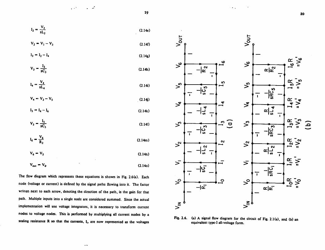
l2~ir2
V2-V,-V3
I3 " h ~ I4
1 -A4 sL4
v4-v3-v5
I5-I4-U
V>-Ic7
u-i
19
(2.14e)
(2.140
(2.14g)
(2.14h)
(2.14i)
(2.14J)
(2.14k)
(2.141)
(2.14m)
v6 " V5 (2.i4n)
voui - V6. (2.14o)
The flow diagram which represents these equations is shown in Fig. 2.6(a). Each
node (voltage or current) is denned by the signal paths flowing into it. The factor
written next to each arrow, denoting the direction of the path, is the gain for that
path. Multiple inputs into a single node are considered summed. Since the actual
implementation will use voltage integrators, it is necessary to transform current
nodes to voltage nodes. This is performed by multiplying all current nodes by a
scaling resistance R so that the currents, Ij, are now represented as the voltages
3
*>
ID i
^>{
1 —
1 *•
1
If) 1
> 1"°
1-te — 1
Ol" 1> '
H-T\u> 1 v
:> '1 *°
' 1 1 to — a
->'' 1 ^, — -k 1 v
> (
-\v1
1 CA— a
-? <> •
—
-1*
?• <>
<£>
IT)
10 r-i
CM
3O
> )
£
I —
1 cua:\cr.1 1
10
>
' 1
1 *°—1°
1 CA— a
•^ (> '
, _
1 *rr_i
1 CO1 v
ro
> '
' T
1 n
' CA — n
CM ,>
1 —
1 "1 CA 1 v
•^ '
rT
prr
1 CO — i.
^?,^
—
rr|rr
Z<>
20
q: ^-5? •»
or T*>10 «>
•—1 II
«• >*-i II
•—• 11-Q
cr "cmCM >
•—• II
°L~^
o >•-• II
Fig. 2.6. (a) A signal flow diagram for the circuit of Fig. 2.1(a), and (b) anequivalent type-1 all-voltage form.

** '
<° ,>
—
1 CM
1 "
m
>
t —
lO
o
CA '
.<*• ,
1
, — 4? -ro
1
i —
ro
— <->
»CA |
CM (>
k —
1 "1CA | V
z> \
'T1°tr ,
1 CA
>°fx|cr
z
T
>I
CD
>
>
>I
CM
>
^
Fig. 2.6. (c) A type-U signal flou diagram for the circuit of Fig. 2.1(a).
21 22
V,'=i<lr In order to maintain the proper relationships between the voltage and
current nodes, the branch gain factors are also scaled by R in Fig. 2.6(b).
There are tradeoffs between capacitor area and filter dynamic range which are
involved in choosing a value for R which will be described in greater detail in
Chapter 4 [40]- [41]. In general, a value of R«l ohm is a good compromise, and
for this case, the integrator time constants are the original L or C values. After
scaling, the terminations, Rj and R2, are realized by connecting the outputs of the
R Rterminating integrators to their inputs multiplied by the gains — and —. The
Ri R2
optimum choice for the values of Rj and R2 depends on many factors, and they will
be assumed to equal 1 ohm in the designs in this chapter.
The flow diagram in Fig. 2.6(b) is one of many that deowribe the ladder of
Fig. 2.1(a). For example, the equivalent flow diagam of Fig. 2.6(c) is useful in the
development of type-H LDI switched capacitor filters which are insensitive to
parasitic capacitances. This technique will be discussed in detail in Chapter 3.
2.5. MOS Switched Capacitor Filter Circuits
Using the signal flowgraph techniques, and switched capacitor integrators,
many types of filters can be designed. This section- will present several design
examples which illustrate the signal flowgraph synthesis procedures.
2.5.1. Doubly-Terminated All-Pole Lowpass Ladder Filler
In the flow diagram of Fig. 2.6(b), it is apparent that the basic element is a
differential integrator. If five switched capacitor differential integrators are intercon
nected as indicated in the flow diagram, the result is the complete switched capaci
tor circuit shown in Fig. 2.7 which closely approximates the RLC network of
Fig. 2.1(a). In this figure, the phasing of the switches is alternated to obtain the

23
Fig. 2.7. A fifth-order switched capacitor type-I LDI doubly-terminatedlowpass ladder filter.
24
type-1 LDI configuration.
The final step in the design is to determine the capacitor ratios required in the
circuit. It will be assumed that R,-R2-R-l ohm and that the element values of
the passive prototype (Cb L2, C3, L4 and Cs) were obtained from standard design
tables so that they correspond to a cutoff frequency of 1 rad/sec [26],[27],[29].
The ratio of the integrating capacitors (CC|, CLj, CC), CLt and CCj in Fig. 2.7) to the
switched capacitors, Cu, can be found from Eqn. (2.7) and the flow diagram:
cu
EhCu
ShiC„
Cct
f«Cl (2.15a)
fcL2(2.15b)
(2.15c)
f±4 (2.15d)
f«Cj (2.15e)
where tu^, is the desired cutoff frequency of the filter, and fc is the sampling fre
quency.
The terminations are paths using unit sized capacitors (assuming 1 ohm termi
nation and scaling resistors) from the output to the input of the first and last
integrators. Unfortunately, there is an extra half cycle delay through the termina
tion loops. This extra delay causes an error in the simulated termination resistance.
In practice, the frequency response error due to this incorrect termination is often
negligible [24], [25],[42].

25
2.5.2. Lowpass Ladder Filter with Finite Transmission Zeros
The addition of finite transmission zeros to a lowpass ladder filter response has
great importance in many filter applications [1]. The zero addition is achieved on
the RLC lowpass prototype by adding feedthrough capacitors across the series arm
of the ladder network such as C2 in Fig. 2.8(a). Imaginary axis zero locations are
the resonant frequencies of the RLC resonant tank circuit, i.e. ow0 - [L2C2]"<)5.
The flow diagram for this network is not as straight forward as for the simple
lowpass case. The usual approach to flow diagram construction of the circuit is suit
able only for continuous-lime active RC implementations because it contains vol
tage attenuators. Usually, this is not desirable in a switched capacitor implementa
tion since additional op amps would be required.
In order to design a switched capacitor network with zeros which does not
require any additional operational amplifiers, it is useful to examine in detail the
operations that are performed by the feedthrough capacitors added to the lowpass
ladder structure. Referring to Fig. 2.8(a), a three-pole, two-zero RLC filter is
shown with voltages and currents defined. Using KirchhofTs current law at
nodes A and B, the following equations are derived to explain the function of C2:
and
(I0-I2)s(Ci+C2)
V,- s(C2+C3) T Y,|C2+C3
+ v,C,+C5
(2.16)
+ v, (2.17)
Thus, C2 has been identified as an element that feeds some of the charge at node A
to node B and vice-versa. As illustrated in Fig. 2.8(b), in order to implement a
complex transmission zero pair, it is necessary to change the integrator gain
V0
* ®R, I
IN
* ®L2 I2
3*C|+C2 1C2-3) Vvi(
(b)
C,+C2
26
R2 VOUT
I0 -z -* -4
^(C,+C2) ?n(C2+C3)
c2c2+c3
!R2 V,OUT
oVquT
Fig. 2.8. <a) An RLC third-order elliptic lowpass ladder filter, and (b) anequivalent form; <ci the corresponding signal flowgraph.

27
constants that represent shunt capacitors to account for the feedthrough capacitor.
This action, along with creating the feedforward and feedback paths, completely
simulates the added series capacitance.
In the switched capacitor implementation, the integrator gain constants are
easily changed by adjusting their capacitor ratios. The paths linking V, and V3 of
Fig. 2.8(c) require the addition of two op amp outputs. Fig. 2.9shows a circuit that
achieves the required integration and addition without additional op amp stages.
The circuit performs a standard sampled-data integration on Vin, and in addition,
continuously multiplies Vx by a constant and sums it to the output. Since Q and
Csare held to a virtual ground on one side by the op amp, Cscharges to Qs~CsVx
and the output due to V„ is given by,
v -_ik«°* c vx. (2.18)
Although the summation is continuous, in the filter, Vx will be derived from
another integrator whose output changes only once every clock cycle. Using
switched capacitor integrator/summers for (Cj+C2) and (C2+C3) in Fig. 2.8(c)
allows the necessary additions at nodes V, and V3. Since the summations involve a
sign inversion, some minor modifications must be made to the flow diagram. For
example, if node V,, the output of an op amp, must contain a fraction of another
node voltage V3, the two voltagesmust be of opposite sign on the flow diagram.
The method described above for obtaining transmission zeros requires very lit
tle additional hardware over the all-pole filter circuit. The example chosen to
demonstrate the design methods of this section is a third-order elliptic filter [25].
The RLC network contains 4 energy storing devices, while the final switched capa
citor circuit shown in Fig. 2.10 requires only 3 operational amplifiers. In addition,
only 2 switches and 4 small capacitors are required over the simple lowpass
28
VqUT
Fig. 2.9. A switched capacitor integrator/summer.

29
Fig. 2.10. A third-order switched capacitor lype-1 LDI doubly-terminatedelliptic lowpassladder filter.
• # « »
30
structure.
2.5.3. Singly-Terminated All-Pole Lawpass Ladder Filter<r
A singly-terminated lowpass fitter is a special case of a-*loubly4erminated RLC
network with an infinite load resistance. Since,the terminations appear as feedback -
paths in the switched capacitor network, the switched capacitor singly-terminated
network is derived from the doubly-terminated network by simply omitting the ter
mination feedback path on the last stage. A singly-terminated fifth-order switched
capacitor lowpass filter is shown in Fig. 2.11.
2.5.4. Doubly-Terminated Bandpass Ladder Filters
The bandpass ladder is obtained by performing the standard lowpass-to-
bandpass transformation on the lowpass prototype of Fig. 2.12(a). This is done by
letting
s —»B
J_ + ^Is (2.19)
where B is the desired bandwidth and m0 is the center frequency as shown in
Table II [43]. Figure 2.12(b) shows a 4-pole RLC bandpass structure after transfor
mation. An all-integrator signal flow diagram for the bandpass ladder is given in
Fig. 2.12(c).
From Eqns. (2.7) and (2.19), the elements in the bandpass network of
Fig. 2.12(b) are found to be
CA-B
QC,
B 1
C,«02 QC|ti>0
(2.20a)
(2.20b)

ET
>Q
.O
.3
)O
—,
Wo
33. o •o
(k!
13
f
re
~i
23
W09
-I
ar
i/>
m—
i
*i
l/l
~*f
—
*•ST
rea
3"2
II
i/>
X
NO
RM
AL
IZE
D
LO
W-P
AS
S
EL
EM
EN
TS
1? o J; 3 Q.
N
CN
1c.
f
HIG
H-P
AS
S
EL
EM
EN
TS
ftCl-N ft
ftc^
N
BA
ND
PA
SS
EL
EM
EN
TS B
Bo
-n
rm
^oL
N
ft
B
n*
cN
'OU
T
BA
ND
-RE
JE
CT
EL
EM
EN
TS
l/B
LN B
CN
BC
no
_m
m.
n§ ft
VS

•^-vw-L2
IN 7kC R2 VOUT
II
*— ioO •MAr *»
Ri
4
VlN | V0 ., V,
(a)
^L £ rV|L LB c
\(r
"U
(b)
33
V4 V0UT
V4| v0UT
Fig. 2.12. (a) An RLC two-pole doubly-terminated lowpass ladder prototype;(b) the RLC four-pole bandpass filter, and (c) the correspondingsignal flowgraph.
and
L2 QL2
B B o>„
L^2 QL2O)0
From the element values above, the capacitor ratios are calculated:
CCa ^ C,fc QC,fcCu B w0
CLA-
BfcC,a»02
„ fcCu QCjtDo
Cu-
B
QL/c
CcB Bfc _ fcCu L^o2 QL2toc
3*
(2.20c)
(2.20d)
(2.21a)
(2.21b)
(2.21c)
(2.21d)
Note that the bandpass circuit has the same form as a lowpass ladder circuit with
two-integrator loops substituted for single integrators. This corresponds to the
-transformations of single lowpass elements into L-Cresonant circuits as dictated by
Eqn. (2.19).
A signal flow diagram for the bandpass ladder is more complicated than that
for the lowpass ladder due to the shunt and series element pairs. A switched capa
citor version of this bandpass filter which is obtained from the flowgraph synthesis
procedure of Section IV is shown in Fig. 2.13.

35
Fig. 2.13. A switched capacitor doubly-terminated four-pole bandpass ladderfiller.
2.5.5. Singly-Terminated Bandpass Ladder I Filter
As in the lowpass case, the singly-termin; atedbandpass ladder is obtained from
the doubly-terminated bandpass ladder by siimply eliminating a termination feed
back loop. A singly-terminated RLC 4-pole: bandpass derived from the singly-
terminated RLC lowpass of Fig. 2.14(a) is shown in Fig. 2.14(b), with its switched
capacitor equivalent circuit in Fig. 2.IS.
2.5.6. Singly-Terminated Highpass Ladder Fiilter
A highpass filter is obtained by performing the standard lowpass-to-highpass
transformation on the RLC lowpass prototype aas indicated in Table II. This is done
by letting
s — (2.22)
which simply replaces all inductors by capaichors and vice-versa. A singly-
terminated RLC highpass ladder filter is shown in Fig. 2.16(a). Figure 2.16(b)
shows the corresponding signal flowgraph whicBi unfortunately cannot be directly
implemented using switched capacitor techniques because summed signals (such as
V2) cannot be accessed and fed forward since the summing is. performed into a vir
tual ground. The intermediate flowgraph of Fig. 2.16(c) can be constructed by
defining some new variables:
v2 - - (V, - Vta) - - V,"
v4--(v3-v2)--v3-
Ii-Ii + Ij-Ia*
I3-l4 + I5-I4.
(2.23a)
(2.23b)
(2.23c)
(2.23d)

Ljrm
V,N R. V
OUT
(a)
L
ft
V,IN Lq^ OdT* r\ V OUT
(b)
Fig. 2.14. (a) An RLC two-pole singly-terminated lowpass ladder prototype;(b) the corresponding RLC four-pole bandpass filter.
37
1—<^ < o ^ =» U-/
=3o
38
Fig. 2.15. A switched capacitor singly-terminated four-pole bandpass ladderfiller.
c'Ii ft^3
V!N 1L23tv23L4 )v*4 R2|tV5 V0UTI4
39
OUT
-1 V/-1 V2-l V3-I V4 1 V5 1> 0 > 9 > 9 >9 > 9 >
v INJ_SC SL SC SL
J_R2
VOUT
6 < 6 / < 6 ^—O • < 0
It 1 I2 1 I3 1 i; 1 I5(c)
Fig. 2.16. (a) A fourth-order singly-terminated RLC ladder filter; (b) theflowgraph for Fig. 2.16(a), and (c) an equivalent intermediateflowgraph.
, V0UT=A/3-1 9 "I
(e)
Fig. 2.16. (d) An iniermediaie flowgraph. and (e) the final flowgraph for thecircuit of Fig. 2.16(a).
40

?-V3 = V0UT
Vm •=
Fig. 2.16. (0 A symbolic implementation of the flowgraph in Fig. 2.16(e)using integrators and summers.
• » » «
41
Fig. 2.16. («> A type-11 LDI switched capacitor fourth-order singly-terminatedhighpass ladder filter.
42

Ti::• i ••
:i
>-3 • .OJ • , •
M> • 'J ' • 1->•' * 1«< •
* *W* • 1>* • !«o • 1
2 i
2 i• i
43
:.s
:..n
Fig. 2.16. <h) A DINAP simulation for the circuit of Fig. 2.16(g) with a300 Hz cutoff frequency when clocked at 128 kHz.
44
The flowgraph of Fig. 2.16(c) is still not realizable due to the signals leaving sum
ming nodes. However, by noting that
*-£-"»-&♦' (2.24a)
V< - V. - - V, (2.24b)
and
I.sLi
+ IisLi
+ L (2.24c)
the signal flowgraph of Fig. 2.16(d) is obtained, which when the signs are appropri
ately modified, results in the flowgraph of Fig. 2.16(e) which is implemented using
integrator/summers in Fig. 2.16(f). Figure 2.16(g) shows the switched capacitor
version, and Fig. 2.16(h) shows a DINAP simulation for a fourth-order singly-
terminated highpass ladder filter with a 300 Hz cutoff" frequency when clocked at
128 kHz.
2.5.7. Doubly-Terminated Highpass Ladder Filter
A signal flowgraph for the RLC doubly-terminated ladder filter of Fig. 2.17(a)
is shown in Fig. 2.17(b). Unfortunately, the continuous loop formed around the
summation path has a gain which isnominally one, so that this network is prone to
oscillation.
One solution to this problem is to use adifferent form of the information con
tained in the signal flowgraph. From the flowgraph of Fig. 2.17(b), the output voltage is
Vou, - V, - V, (2.25)

Ri L
* I «-
Co T
i(^2Vo V2V.n "" L, 3|V! 2L3 3|V3 R2;
It ?I3 \U
(a)
(b)
45
VoUT
Fig. 2.17. (a) A third-order doubly-terminated highpass ladder filter and(b) a signal flow diagram.
46
(c)
Fig. 2.17. (c) A symbolic representation of Fig. 2.17(a) using integrators andsummers.

n::
c3:«cs . .«
5-3::e .<
>c. •»
Mi;
:1...J.
47
51
Fig. 2.17. (d) A DINAP simulation for the circuit of Fig. 2.17(c) with a300 Hz cutoff frequency when clocked at 128 kHz.
48
and the other output variables in the circuit are I,, and 13. A doubly-terminated
structure can be formed by solving for all of the output variables in terms of them
selves and the input voltage to obtain:
and
I'-sy-(-v*)-,«-v--4
v - (-Vin> II I3 1 ,
-i-v3 - -1- vsL3 3 sL3 out'
(2.26a)
(2.26b)
(2.26c)
A symbolic representation of these equations is shown in Fig. 2.17(c) with a
DINAP simulation in Fig. 2.17(d) for a 300 Hz cutoff frequency when clocked at
128 kHz. Since there are no continuous loops, this circuit will not be subject tooscillation.
2.5.8. Doubly-Terminated Elliptic Highpass Ladder Filter
Many applications require ahighpass response with additional rejection of cer
tain frequencies. A doubly-terminated RLC elliptic highpass filter is shown in
Fig. 2.18(a). This circuit can be simplified by solving for V, and V3
"l^fel*-1^ (2.27a)
and
V3-skt£H(l2-l4)+U->L2+L3 L2+L3 (2.27b)

49
to obtain the equivalent circuit for the elliptic highpass shown in Fig: 2.18(b).
Using an equation formulation similar to that of the previous section, the circuit of
Fig. 2.18(c) is derived with a DINAP simulation shown in Fig. 2.18(d). An advan
tage of this formulation over a direct four amplifier implementation is that by form
ing the equivalent circuit of Fig. 2.18(b), the large L2 value is reduced by paralleling
it with the two smaller inductors, L, and L3,and therefore, the required silicon area
is greatly reduced.Ri
o—WW
IlA L2f>rrm1
V,| °L13lV1 2L3^V3R2|tV4V0UTfit fc fc
o- • • m m < m
(°)
RHoft
<D
v0 I v2 tbL L ,
v,N H LfL2 p1 v, v3 [ v4: •R:
V, V,L+L-n'I, 'L2+L3Vri "I.
(b)
V,OUT
Fig. 2.18. (a) A doubly-terminated RLC third-order elliptic highpass filter,and (b) an equivalent form.
50

(c)
Fig. 2.18. (c) A symbolic implementation of Fig. 2.18(a) using integratorsand summers.
51
i::
I::
-3:*—* •
131
f It'••? t
r.
n
I
"i 1
Fig. 2.18. (di A DINAP simulation for the circuit of Fig. 2.18(a) with a300 Hz cutoff frequency when clocked at 128 kHz.
Chapter 3
CONSIDERATIONS FOR THE MONOLITHIC MOSIMPLEMENTATION OF SWITCHED CAPACITOR FILTERS
53
In the monolithic MOS implementation of switched capacitor ladder filters,
there are several important effects which must be considered including: (1) The
finite switching frequency of the sampled-data system; (2) nonidealities associated
with the passive MOS switches and capacitors, and (3) nonidealities associated with
the operational amplifiers. These practical design aspects will be considered in this
chapter.
3.1. Sampled-Data Discrete-Time Effects
Switched capacitor fillers are analog discrete-time systems which, in many
cases, are derived from continuous-time RLC prototypes. In this section, the
effects of transforming from the continuous- to the sampled-data domain are
described.
3.1.1. Continuous-Time RC Integrators
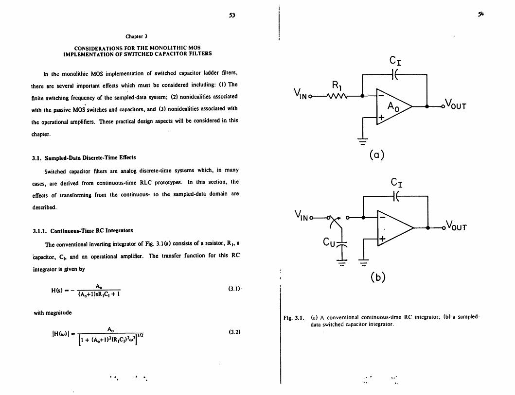
The conventional inverting integrator of Fig. 3.1(a) consists of a resistor, Rj, a
capacitor, C|, and an operational amplifier. The transfer function for this RC
integrator is given by
H(s) - -
with magnitude
|H(o>)|-
(A0+l)sR,C, + 1
T72"[l +(Ao+O'CRA)2*2]
(3.1)
(3.2)
54
VR
INo VWV
OUT
(°)
1-hMovOUT
(b)
Fig. 3.1. (a) A conventional coniinuous-time RC integrator; (b) a sampled-data switched capacitor integrator.

and phase
<P(cu) - - it - tan-,&>R A(A0+1)
55
(3.3)
where Ao is the DC open-loop gain ofan otherwise ideal op amp. The magnitude
asymptotes and phase of Eqns. (3.2) and (3.3) are plotted in Figs. 3.2(a) and (b),
respectively. From Fig. 3.2(a), it isevident that finite op amp gain results ina lossy
integrator with an error in the integrator bandwidth. To reduce this error to less
than 1%, the op amp is required to have Ao greater than 100, and when A0 is
greater than 1000, the integrator gain constant error is less than 0.1%. If Ao is
infinite, the transfer function of Eqn. (3.1) becomes
H(s) - - =±s
or equivalently,
H(ai) - - t-2-
(3.4a)
(3.4b)
with £i>0=——. The characteristics of analog sampled-data integrators will beRA
presented in the next section.
3.1.2. Discrete-Time Switched Capacitor Integrators
An important difference between the conventional RC integrator of
Fig. 3.1(a), and the switched capacitor integrator of Fig. 3.1(b) is that the latter
usually only samples the input signal once each clock cycle. Hence, there can be a
time delay through the integrator of up to one full clock period. The excess phase
shift associated with this time delay can result in significant Q-enhancement if a
switched capacitor integrator is used to directly replace a conventional RC integrator
H(f)
o foAo+1
-180
-210 -•
-240 »
fn=0" ZlTR^Cj
(a) .^'^T°VAo+l
>-t™\fA£l-270 " <£(f)
(b)
Fig. 3.2. (a) The magnitude ..nd (b) the phase plots for an RC integratorwith A„ representing the op amp DC open-loop gain.

57
in an active ladder circuit. This phase shift can complicate the design, but more
importantly, can break down the analogy of the design with the RLC passive ladder
prototype. If this happens, the low sensitivity obtainable with a doubly-terminated
ladder may be lost. Fortunately, the effect of this deleterious phase shift can be
almost completely eliminated.
In order to analyze the effect of the time delay, it is useful to develop a z-
transform model of the inverting integrator of Fig. 3.1(b) (assuming an ideal op
amp) [38]-[39]. The switched capacitor, Cu, will be charged to the input voltage,
Vm(t), at the beginning of each clock period, and will be switched to the op amp
virtual ground halfway through each cycle. Therefore, at the beginning of the n,h
clock period (i.e. t«nTc), the switch is in the left position, and Cu has a charge
Qc "CuVjnGiTc). The value of the output signal at this time is stored as the
charge, QC|, on the integrating capacitor, C|. Its value was determined a half cycle
earlier at t=(n-l/2)Tc and therefore, QC|=C|V0U,((n-l/2)Tc). At the next half
cycle time, t«=(n+l/2)Tc, the switch is in the right position, and the capacitor Cu is
discharged by the op amp as the charge is transferred from Cu to Cj. The charge
on C| is now
C,V0Ut[(n+l/2)Tc] - C,Voul[(n-l/2)Tc] - CuVjn(nTc).
The transfer function taken at this half cycle time, H1/2(z), is therefore
Hwfc> - -cu
c«
z-l/2
l-z"V
(3.5)
(3.6)
where the subscript 1/2 indicates that there is only 1/2 clock cycle of delay in the
forward path of this integrator. An integrator with this half-delay property is
known as a type-I Lossless Discrete Integrator (LDI) [42].
58
For the next half clock period from (n+l/2)Tc to (n+l)Tc, (i.e. during the
sampling interval), the output does not change, which yields another half cycle of
delay. Therefore, the transfer function of the integrator taken at the end of this
interval (at t-(n+l)Tc) has a full cycle of delay in the forward path and is given by,
H,(z) - -cu z"1
i-z"V(3.7)
This integrator is called the Direct-Transform Discrete Integrator (DDI) [42].
The type-I Lossless Discrete Integrator of Eqn. (3.6) has exactly the same
phase shift as a continuous-time integrator [42]. However, the DDI integrator
represented by Eqn. (3.7) has significant excess phase. To illustrate this result, the
frequency responses of H1/2(z) and Hj(z) are evaluated by setting z^e"" ' to obtain
and
Hi/2(oi) •» —-r2-jo*
wTc
2sin(o»-^-)
jwH,(6,)--T^
T6>Tcexp(-jo)-^-)T2sin(o>-y-)
(3.8)
(3.9)
with cu0=fc These expressions are factored so that the term in brackets is the
deviation from the response of the continuous-time integrator given in Eqn. (3.4b).
Table I shows that the sampling frequency must be large relative to the
passband frequencies in order to minimize the error in the magnitude of the
integrator bandwidth in Eqns. (3.8) and (3.9). (For the designs of this thesis, the
clock frequency was typically 35 times greater than the maximum passband
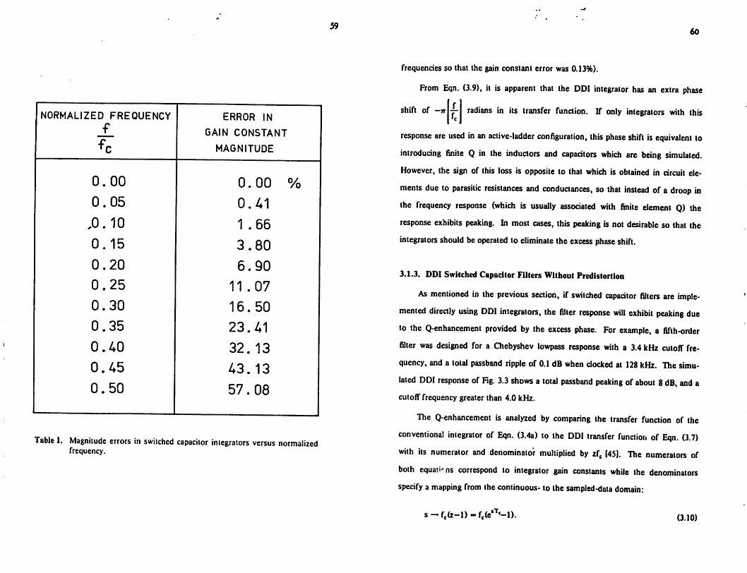
NORMALIZED FREQUENCY ERROR IN
f GAIN CONSTANT
*C MAGNITUDE
0.00 0. 00 %
0.05 0.41
,0.10 1 .66
0.15 3.80
0.20 6.90
0.25 11.07
0.30 16.50
0.35 23.41
0.40 32.13
0.45 43.13
0.50 57.08
Table I. Magnitude errors in switched capacitor integrators versus normalizedfrequency.
5960
frequencies so that the gain constant error was 0.13%).
From Eqn. (3.9), it is apparent that the DDI integrator has an extra phase
shift of -it — radians in its transfer function. If only integrators with this
response are used in an active-ladder configuration, this phase shift is equivalent to
introducing finite Q in the inductors and capacitors which are being simulated.
However, the sign of this loss is opposite to that which is obtained in circuit ele
ments due to parasitic resistances and conductances, so that instead of a droop in
the frequency response (which is usually associated with finite element Q) the
response exhibits peaking. In most cases, this peaking is not desirable so that the
integrators should be operated to eliminate the excess phase shift.
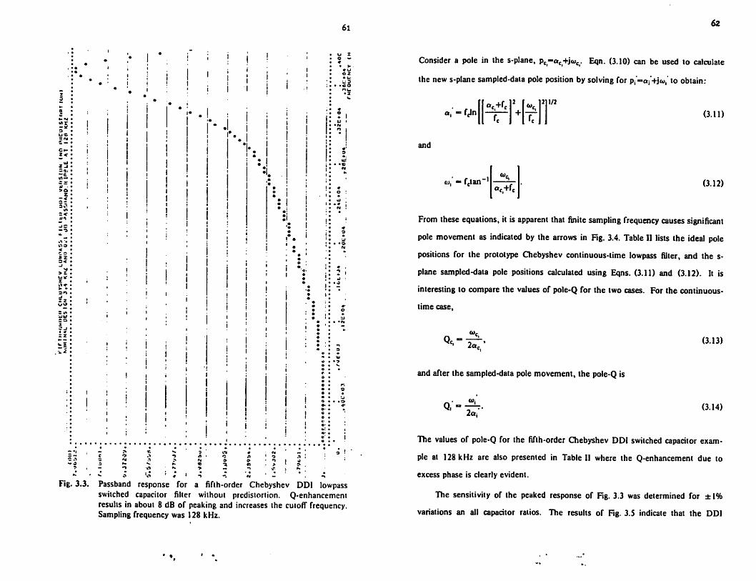
3.1.3. DDI Switched Capacitor Filters Without Predistortion
As mentioned in the previous section, if switched capacitor filters are imple
mented directly using DDI integrators, the filter response will exhibit peaking due
to the Q-enhancement provided by the excess phase. For example, a fifth-order
filter was designed for a Chebyshev lowpass response with a 3.4 kHz cutoff fre
quency, and a total passband ripple of 0.1 dB when clocked at 128 kHz. The simu
lated DDI response of Fig. 3.3 shows a total passband peaking of about 8dB, and a
cutoff frequency greater than 4.0 kHz.
The Q-enhancement is analyzed by comparing the transfer function of the
conventional integrator of Eqn. (3.4a) to the DDI transfer function of Eqn. (3.7)
with its numerator and denominator multiplied by zfc [45]. The numerators of
both equations correspond to integrator gain constants while the denominators
specify a mapping from the continuous- to the sampled-data domain:
•Tc.s-fc(z-l)-fc(e,T«-l) (3.10)
— «3-3 k-!
il*> •
anj
r zUV»
SlA
i i
61
r.
i *
Fig. 3.3. Passband response for a fifth-order Chebyshev DDI lowpassswitched capacitor filter without predistortion. Q-enhancemcntresults in about 8 dB of peaking and increases the cutoff frequency.Sampling frequency was 128 kHz.
62
Consider a pole in the s-plane, pc-ac+jwCi. Eqn. (3.10) can be used to calculate
the new s-plane sampled-data pole position by solving for pi"a{+}ut- to obtain:
and
gnK+fc 2
+
2
II fc 11/2
fctan-i
<*c+fc
(3.11)
(3.12)
From these equations, it is apparent that finite sampling frequency causes significant
pole movement as indicated by the arrows in Fig. 3.4. Table II lists the ideal pole
positions for the prototype Chebyshev continuous-time lowpass filter, and the s-
plane sampled-data pole positions calculated using Eqns. (3.11) and (3.12). It is
interesting to compare the values of pole-Q for the two cases. For the continuous-
time case,
Qc 2<(3.13)
and after the sampled-data polemovement, the pole-Q is
*••$ (3.14)
The values of pole-Q for the fifth-order Chebyshev DDI switched capacitor exam
ple at 128kHz are also presented in Table II where the Q-enhancement due to
excess phase is clearly evident.
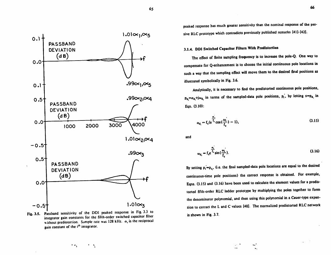
The sensitivity of the peaked response of Fig. 3.3 was determined for ±1%
variations an all capacitor ratios. The results of Fig. 3.5 indicate that the DDI

CT t/i •wo
3" rere rr**. re 3
o«»
re*
a.
o09
OS 3i/i 0></> o 3m o
"*
re-<
Q.-i C
3 re
3re
•70 o03
aO
reQ.
09
Xoreto
^^ in
tO mOO X •a
XN
as 3*
3 09(A
T3 re
re03v>
i/io
*-»n
o 09•^
re
cs a.
3) *<re 3*
•ao
3*re re
n3*re
OD
"0O V
en y
x
TJo
•i
m
•o to >o > toi— T 70m T» o
r* *i rn eno o< i zm
>
go
m H >z > •H-H m
.J0.
oz o
m
o >X r-mCD TJ-< Oto r~X mm
-o < -da o
ro in (0r~
X i— -i
i ^ -o TJ oX V o to z
TJ \"* m to»o N
X
o o -v*II to I
^ to Sru -n o• o o
70 H
TJOr-m
p=.sn^ J r%IS. §
~ £"*•o / " 2.
5 i £3o" ri. D 3
•5' re ?J 2.•0 ^ 3- n
g..Sc•a "• o 3
5' Hi 2 w_, =r a, o.
» 3. 5 5* re «» re
- n 5. _,N> 3- J y00 re 03 -1
*• °* 3 -K " °" 2"N 3" < »
" 3 1-3
** I»asj? £' s—• o ««~ -i re
CONTINUOUS
CASE
DDI SAMPLED
DATA CASE
(128 KHZ)
PREDISTORTED DDI
SAMPLED DATA
CASE (128 KHZ)
NORMALIZEDPOLE
POSITIONS
POLEQ
NORMALIZEDPOLE
POSITIONS
POLEQ
NORMALIZEDPOLE
POSITIONS
POLEQ
-0.1665
-j1.08043.24 -0.0676
-j1.09828.12 -0.2585
-j1.04462.02
-0.4360
-j 0.66770.77 -0.4095
-j0.71630.87 -0.4548
-j 0.61930.68
-0.5389
♦j 0.00000.00 -0.5644
♦j 0.00000.00 -0.5151
♦j 0.00000.00
-0.4360
♦j0.6677
0.77 -0.4095
♦j 0.71630.87 -0.4548
♦j 0.61930,68
-0.1665
♦j 1.08043.24 -0.0676
♦j 1.09828.12 -0.2585
♦j 1.04462.02
a.OS
ON
0.1"
0.0
o.i--
0.5-"
0.0
-0.5--
0.5-'
PASSBAND
DEVIATION
(dB)
PASSBAND
DEVIATION
(dB)
1000
PASSBAND
DEVIATION
(dB)0.0' —
-0.5"'
65
1.01©<i,o<5
^cx^o^
.99cx2,cx4
2000
I.OICX3
Fig. 3.5. Passband sensitivity of the DDI peaked response in Fig. 3.3 tointegrator gain constants for the fifth-order switched capacitor fillerwithout predisionion. Sample raic was 128 kHz. o, is the reciprocalgain constant of the i,h integrator.
66
peaked response has much greater sensitivity than the nominal response ofthe pas-
RLC prototype which contradicts previously published remarks [411-142].sive
3.1.4. DDI Switched Capacitor Filters With Predistortion
The effect of finite sampling frequency is to increase the pole-Q. One way to
compensate for Q-enhancement is to choose the initial continuous pole locations in
such away that the sampling effect will move them to the desired final positions as
illustrated symbolically in Fig. 3.6.
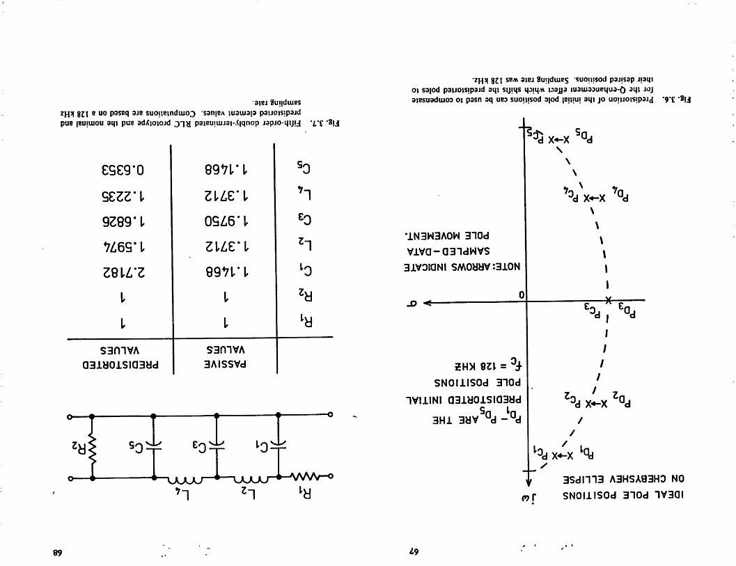
Analytically, it is necessary to find the predistorted continuous pole positions,
pd-ad+ja>di in terms of the sampled-data pole positions, p-t by letting s-pdi in
Eqn. (3.10):
and
ad-fc(ef«cos(y-)-l),1 'c
—1 •
o)d -fce^sinO^-).1 *c
(3.15)
(3.16)
By setting Pj'=pCi, (i.e. the final sampled-data pole locations are equal to the desired
continuous-time pole positions) the correct response is obtained. For example,
Eqns. (3.15) and (3.16) have been used to calculate the element values for apredistorted fifth-order RLC ladder prototype by multiplying the poles together to form
the denominator polynomial, and then using this polynomial inaCauer-type expan
sion to extract the Land Cvalues 148). The normalized predistorted RLC network
is shown in Fig. 3.7.
IDEALPOLEPOSITIONS
ONCHEBYSHEVELLIPSE
J6>
A
67
"biX-*XR
C1
x-*x?,
X-^XP,
Pn-PnARETHED1u5
PREDISTORTEDINITIAL
POLEPOSITIONS
fc=128KHZ
->»cr
NOTE:ARROWSINDICATE
SAMPLED-DATA
POLEMOVEMENT.
pD5X-XP,*i-
Fig.3.6.PredistortionoftheinitialpolepositionscanbeusedtocompensatefortheQ-enhancementeffectwhichshiftsthepredistortedpolestotheirdesiredpositions.Samplingratewas128kHz.
RiL20-\\V\r-t-nrnrV
_mm_»
?kCi^tnC3•"1-^5R2
PASSIVEPREDISTORTED
VALUESVALUES
Ri11
R211
Ci1.U682.7182
L21.37121.5974
c31.97501.6826
L*1.37121.2235
c51.14680.6353
68
Fig.3.7.Fifth-orderdoubly-terminatedRLCprototypeandthenominalandpredistortedelementvalues.Compulationsarebasedona128kHzsamplingrate.

69
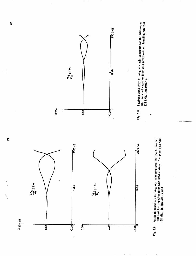
The predistorted switched capacitor fifth-order lowpass filter has been simu
lated at a 128 kHz clock rate for a ±1% variation on all capacitor ratios with life
results given in Fig. 3.8. Compared to the RLC prototype, the predistortion has
increased the sensitivity by about a factor of 10. In the limit of higher clock rates,
switched capacitor integrators approach continuous-time RC integrators, and the
sensitivity of the switched capacitor filter approaches that of the continuous proto
type. However, as the clock rate increases, the required capacitor ratios also
increase resulting in an area-sensitivity tradeoff. Hence, a method of filter design
which does not require predistortion is desired. By using Lossless Discrete Integra
tors, predistortion can be avoided in many cases, and nearly ideal sensitivity may be
obtained. The LDI filter properties are described in the next two sections.
3.1.5. Type-I LDI Switched Capacitor Filters
The phasing of the switched capacitors of integrators which are connected
together determines whether the frequency response of the integrator is given by
H1/2(co) or Hi(u). The two integrator loop of Fig. 3.9 demonstrates the proper
switch phasing required to obtain the H,/2(o») transfer function. The signal at the
output of integrator 2 is available as soon as the switched capacitor is connected to
the op amp, so in order to avoid the extra half cycle of delay (and the resulting
H|(b>) response), the switches of the first integratormust be phased to immediately
sample that output as shown in the figure. Therefore, the switches of adjacent
integrators should be thrown in opposite directions as shown in Fig. 3.9. Integra
tors which are clocked to achieve this half-delay property are used in the implemen
tation of what will be referred to as type-1 LDI switched capacitor filters. A com
plete schematic for the type-I LDI doubly-terminated fifth-order all-pole lowpass
switched capacitor ladder filter is shown in Fig. 3.10.
0.2JT dB
0.00-
-0.20;0
0.20t
0.00-
-0.20-
FIFTH ORDER CHEBYSHEV FILTER = 0.1 dBSAMPLED DATA VERSION WITH 1*P=0.01(AFTER OPTIMIZATION) Eg
1666
CU
1666
70
3570 HZ
3570 HZ
Fig. 3.8. Passband sensitivity to integrator gain constants for the fifth-orderDDI switched capacitor filter with predistortion. Sampling rate was128 kHz. Integrators 1 and 2.
71
0.2
0T
dB
0.0
0-
-0.2o[
16
66
35
70
HZ
0.2
0t
0.0
0
-0.2
01
66
63
57
0H
Z
Fig.
3.8.
Passb
and
sens
itivit
yto
integ
rator
gain
cons
tant
sfor
the
fifth-
orde
rDD
Isw
itche
dca
pacit
orfilt
erwi
thpr
edist
ortio
n.Sa
mplin
gra
tewa
s12
8kH
z.In
tegr
ator
s3
and
4.
0.2
0t
0.0
0
-0.2
0
7-§±
1%CU
16
66
72
35
70
HZ
Fig.3
.8.Pa
ssban
dse
nsitiv
ityto
integ
rator
gain
cons
tants
forthe
fifth-o
rder
?.o\?
ritCh
edca
paci,
orfiI,
erw«
l"Pr
edist
ortio
n.Sa
mplin
grat
ewa
s12
8kH
z.In
tegr
ator
5.

Fig. 3.9. A two-integrator loop which demonstrates the proper switch phasingrequired to obtain the type-I LDI integrators. Clock phases arealternated between stages.
73 7*
Fig. 3.10. A fifth-order lowpass type-I switched capacitor doubly-terminatedladder filter.

75
The
passbandsensitivity
ofthe
filterof
Fig.3.10has
beendeterm
inedfor
±1%
variationson
allcapacitorratios.A
sshow
nin
Fig.3.11,thew
orst-casesensi
tivityofthe
LD
Inetwork
isabout
5tim
eslow
erthan
thatofanequivalent
predis
tortedD
DI
network
fora
128kH
zsam
plingfrequency.
Unfortunately,
thehalf-delay
LD
Irealization
usesthe
topplates
ofthe
switched
capacitorsas
invertingintegrating
inputs,andtherefore,the
resultingfre
quencyresponse
isslightly
inerror
dueto
thetop-plate
parasitic.T
heL
DI
approachdescribed
inthe
nextsectionelim
inatesthis
sourceof
error,and
inaddi
tion,sim
plifiesthe
clockphasing
requirements.
3.1.6.T
ype-IIL
DI
Switched
Capacitor
Filters
Byusing
onlythe
bottomplates
ofsw
itchedcapacitors
asintegrating
inputs,
theerrors
dueto
top-plateparasitics
areelim
inatedsince
ideally,thereis
novoltage
changeon
thetop
plateduringsw
itching,and
thebottom
plateis
switched
between
voltagesources.
The
noninvertingintegrator
ofFig.3.12(a)
hasa
z-planetransfer
fun
ction
of
-l
H,<
Z)-|^"
ZC
i1
-z"1
which
canbe
written
inth
efrequency
domain
as
H,(c)
--r2-
Tw
TjexpHw
-y-)T
2sin(<i>-^-)
(3.1
7a)
(3.1
7b
)
The
circuitofFig.3.12(b)
performs
theinverting
integrationfunction
with
thez-
planetransfer
functionof
76
Fig.3.11.
Passbandsensitivity
for±
1%
variationsin
-zr-w
hichis
the
worst-case
forthe
filtero
fFig.
3.10.S
ampling
ratew
as128
kHz.

77
ovOUT
V,INO o/^*. o
OUT
I-o/v* o—oV|N
(b)
Fig. 3.12. (a) Type-11 noninverting and (b) inverting switched capacitorintegrators. Bottom plates are used as inputs to eliminate errorsdue to the lop-plate parasitic.
H«(z) - --i1-z
which can also be expressed, as
H0(c) - - -r*
TcuTcexp(+w-^-)T2sin(<u-^-)
78
(3.18a)
(3.18b)
It can be seen from Eqn. (3.17b) that the noninverting integrator has excess
phase-lag while the inverting integrator of Eqn. (3.18b) has a phase-lead response.
These integrators will be used in the implementation of type-II LDI switched capa
citor filters.
A two-integrator loop using type-II LDI integrators is shown in Fig. 3.13. By
using the same clock phasing on both stages, the leading and lagging phase com
ponents cancel around the loop, and the correct frequency response is obtained.
The considerations for synthesis of type-II LDI filters are slightly different
than for the type-I case. For the type-II designs, it is desirable to synthesize the
circuits so that the signs of the integrating inputs alternate between stages, i.e., all
even stages positive and all odd stages negative or vice-versa. This sign alternation
allows for the same clocking on all stages, is consistent with existing ladder syn
thesis approaches (491- (501, and provides a direct relationship to the DINAP simu
lation methods to be discussed in Appendix 3. A type-II LDI fifth-order all-pole
lowpass filter is shown in Fig. 3.14. (Refer to the corresponding type-II LDI flow
diagram of Fig. 2.6(c)).
Several workers are independently investigating the use of type-11 LDI integra
tors for telecommunications applications; early indications are that excellent results
will be obtained with this approach (511-152].

o00
o\
o
CM
H
t—+ '—Ii«r* 1
^e^tID
o
u Hi-
M
ao
•o
•o
Q-1
en i^
SO *tf
TJu. -O4> CO
* E
00 .i
2 "
o
O SO
E £>at a»
'.E•*G
||•_ c
2 "5 ">2| fton C n
2 o «>c — =
"T "O eaO « w
cr _
< 2f 3

81
3.1.7. LDI Switched Capacitor Filters With Predistortion
As mentioned earlier, both the DDI and LDI integrators experience a fre
quency dependent magnitude error. Table 1shows that when the signal frequency
approaches the Nyquist rate, -y, the error in the integrator gain constant
approaches 57%! Hence, it is obvious that for high frequency (relative to the sam
pling frequency) switched capacitor filters, the magnitude error must be compen
sated by using predistortion. The type-I LDI transfer function of Eqn. (3.6) maps a
continuous s-plane pole into a sampled-data s-plane pole by the transformation
s—ft[z,/2-z-1/2j - 2f^inh s
2fc
With s-ad+jtDd(, and s'-Oi'+joij', Eqn. (3.19) is solved to obtain:
and
odi - 2fcCOSCDj'
sinh
-<-jtf"g cosh2fc
(3.19)
(3.20)
(3.21)
By letting pj'—pv Eqns. (3.20) and (3.21) can be used to calculate the predis
torted LDI pole positions. This predistortion technique can also be used to com
pensate for other types of nonidealities such as finite op amp gain.
82
3.1.8. Switched Capacitor Filters with Multiple Sampling Rates
In sampled-data systems such as switched capacitor filters, one of the most
difficult practical problems is the requirement for a continuous-time antialiasing
prefilter. The prefilter specifications are reduced by sampling at many limes the
passband frequencies, but unfortunately, this higher sampling rate results in larger
capacitor ratios. An optimum solution to this problem is to operate the first
stage (s) of the filter at a very high sampling rate to ease the prefilter requirements,
and to operate the other stagesCs) at a lower clock rate in order to simultaneously
reduce the silicon area requirements.
This approach has been verified by DINAP simulation for a third-order Che
byshev lowpass filter with a 3.4kHz cutoff and 0.1 dB passband ripple. In Fig. 3.15,
the first stage is switched at 1.024 MHz, and the second and third stages are
switched at 128 kHz. The switches are operated to obtain zero excess phase shift
around all interior two-integrator loops, which requires that the second stage in this
example has its two switched capacitors operating at two different sampling rates as
shown in the figure. The DINAP simulations shown in Fig. 3.16 agree closely with
the expected values.
This technique can also be used to provide a high sampling frequency stage(s)
at the output of the switched capacitor filter so that continuous-time post filtering, if
necessary, becomes easier.
3.2. Passive Component Nonideal Effects
In this section, the effects of nonidealities associated with the passive filter ele
ments will be considered (25],[46].

rC||>
TN
£<~V|£<>
83
Vi
I&5T
LL
l>L
Uf£/e
Lfc
imy
jjj^^
-•
o
v3=v0U
T
Fig.3.15.
Athird-order
lowpass
type-IIL
DIsw
itchedcapacitor
filterw
ithtw
odifferent
sampling
frequencies.
es
-X
J>
-3
at
JC
JO
<I9
.JC
>—
<r
•i
i•
Bk.1U
oz
•-J
•m
o«
-j
—-»
O•y
AO
m•3
rj
Mo
a«
»n
an
0lO
o•»
nn
No
*-»
«in
O9
•rj
0o
»s
A)
Fig.3.16.(a)
TheD
INAPresponse
forthe
circuitofFig.3.15with
128kH
zand
1.024M
Hz
sampling
rates.

— n
«v3-3
9X-u •oo
— X
itX 1
OS
* — r>
Z •3*.« an
— o
• I
I I
! •
Fig. 3.16. (b) The DINAP passband response for the circuit of Fig. 3.15.
85
ez
86
3.2.1. MOSFET Channel (Switch) Resistance
Finite MOSFET switch resistance limits the rate at which charge is transferred
through aswitched capacitor circuit. In order to isolate this effect from opamp set
tling effects (which will be shown to be dominant), it will be assumed that the op
amp in the switched capacitor integrator of Fig. 3.17(a) is ideal. During the sam
pling interval, d«,, the charging network can be represented as the series RaveCu
combination shown in Fig. 3.17(b) where R,ve is the average switch resistance. For
an input voltage of AVj,,, the voltage on Cu at theend of the sampling interval is
Vu(T,)-AVin(l-e R'"c")
where T, is the "on" timeof «>,. The charge on Cu after 0, is
t,
QU(T,) - CUVU(T,) - CuAV^l - e_R-c-).
(3.22)
(3.23)
During the integration phase, <f>2t the op amp attempts to transfer the charge from
Cu to Cj as indicated in Fig. 3.17(c). The voltage on Cu after the integration inter
val, T2, is
VU(T2) - Vu(T,)e R~c" (3.24a)
with a charge of
-Ti
QU(T2) - CUVU(T2) - CuVu(T,)e R-c-. (3.24b)
The total change in charge on Cu during one complete clock cycle, AQU-QU(T,)-
Q„(T2), is given by
AQ0 - CuAVto(l - e ""Sd-e R""c"). (3.25)

87
Since AV0U1-——2-, the integrator gain is
AV,AV,„ - |*|fl-.«>(!-. «•*>. (3.26)
Hence, incomplete charge transfer due to non-zero switch resistance is equivalent
to a capacitor ratio error. If the values of T, and RaveCu are chosen so that the
error is less than 1%, Eqn. (3.26) suggests that Ts should be greater than 5.3 RlveCu
time constants, while for a 0.1% error, 7.6 time constants are required. For the
designs of this dissertation, the Tt intervals were typically 75 time constants making
this effect negligible in comparison to settling errors which will be described later.
3.2.2. MOSFET Nonlinearity and Threshold Voltage Effects
Since the MOS transistors are being used as charge switches, nonlinearity in
the channel resistance is unimportant provided that the charging and discharging
intervals are sufficiently long. However, the threshold voltage of the switches must
becarefully considered. Asan illustration of this point, suppose in Fig. 3.17(a) that
Cu is initially at 0 volts when *, and V^ are connected to VDD. When Vu has risen
to within a threshold voltage of VDD, the switch transistor turns off. Hence, the
input signal may be clipped, resulting in a decrease in the dynamic range of the
filter. In single channel MOS technology, bootstrapped clock drivers can be used to
overcome this problem, and in CMOS technology, transmission gates can be used
to obtain full voltage swings.
V,IN o
V
- (a) -
Ravein o WW
(b) -
Cu^k
-ov0UT
u
oVQUT
Fig. 3.17. (a) A switched capacitor integrator, and the RC circuit models for(b) the sampling phase, and (c) the integration phase.
88
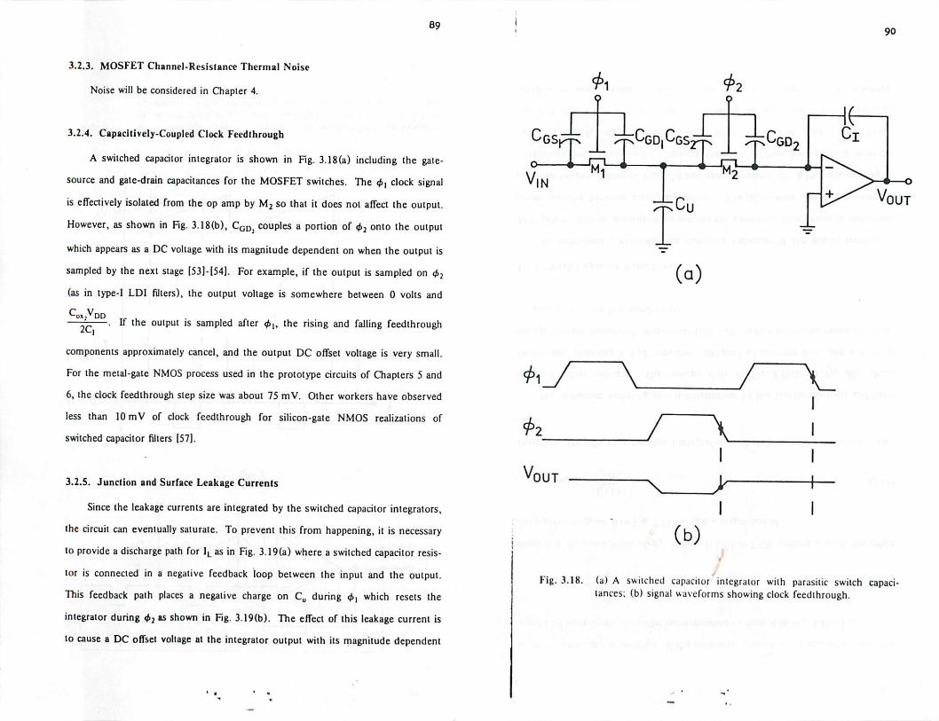
89
3.2.3. MOSFET Channel-Resistance Thermal Noise
Noise will be considered in Chapter 4.
3.2.4. Capacitively-Coupled Clock Feedthrough
A switched capacitor integrator is shown in Fig. 3.18(a) including the gate-
source and gate-drain capacitances for the MOSFET switches. The 0, clock signal
is effectively isolated from the op amp by M2 so that it does not affect the output.
However, as shown in Fig. 3.18(b), CGDj couples a portion of <f>2 onto the output
which appears as a DC voltage with its magnitude dependent on when the output is
sampled by the next stage [53]-[54]. For example, if the output is sampled on <f>2
(as in type-I LDI filters), the output voltage is somewhere between 0 volts and
Coxj^DD Tf .———. If the output is sampled after <£,, the rising and falling feedthrough
ZL-i
components approximately cancel, and the output DC offset voltage is very small.
For the metal-gate NMOS process used in the prototype circuits of Chapters 5 and
6, the clock feedthrough step size was about 75 mV. Other workers have observed
less than 10 mV of clock feedthrough for silicon-gate NMOS realizations of
switched capacitor filters [57].
3.2.5. Junction and Surface Leakage Currents
Since the leakage currents are integrated by the switched capacitor integrators,
the circuit can eventually saturate. To prevent this from happening, it is necessary
to provide a discharge path for IL as in Fig. 3.19(a) where a switched capacitor resis
tor is connected in a negative feedback loop between the input and the output.
This feedback path places a negative charge on Cu during </>, which resets the
integrator during 4>2 as shown in Fig. 3.19(b). The effect of this leakage current is
to cause a DC offset voltage at the integrator output with its magnitude dependent
*i 4>:
GSp-p [CGDjCGSrfN — CGd-o-
V, N
M
*i_y^~A
&
V,OUT
-f <> u
^C u
(a)
J v_
/ \
X >
(b).
90
Fig. 3.18. (a) A switched capacitor integrator with parasitic switch capacitances; (b) signal waveforms showing clock feedthrough.

1J~L
Vu?fcCu IL(t) r
(a)
91
Fig. 3.19. (a) A switched capacitor integrator with negative feedback to stabilize against the leakage current, and (b) the corresponding voltagewaveforms. Effective offset depends on sampling instant at theoutput.
92
on when the output is sampled. If the output is sampled at the end of <f>2 as in the
type-I LDI integrators, the offset corresponding to time A in Fig. 3.19(b) is
'OS, C '(3.27)
where t is the pulse width of <J>2. If type-II LDI or DDI clocking is used, the offset
corresponds to point B in Fig. 3.19(b) with a magnitude of
1l(T+t)2C,
(3.28)
Therefore, the offset for the type-I integrators is slightly less than in the other two
cases.
The minimum sampling rate is determined by the leakage currents and their
resultant offset voltages. The voltage drift in Fig. 3.19(b) is typically about
10mV/sec, assuming a 1 pF capacitor, 100 fim7 of junction area, and a thermal
leakage current density of 10nA/cm2 [55]. This effect limits the minimum sam
pling frequency to a few hundred Hz.
3.2.6. MOS Capacitor Ratio Errors
As mentioned previously, the passband response of the doubly-terminated
RLC ladder filter is insensitive to component variations when there is maximum
power transfer between input and output. The fifth-order type-I LDI switched
capacitor lowpass ladder of Fig. 3.10 has been simulated for ±1% variations on all
integrator capacitor ratios with a nominal Chebyshev design having a total passband
ripple of 0.1 dB, and a cutoff frequency of 3.4 kHz when clocked at 128 kHz.
Fig. 3.11 shows that the worst-case deviation in the passband is only ±0.022 dB
which is in close agreement with the sensitivity of the passive RLC prototype.

93
Previous work has shown that monolithic capacitors can easily be matched to within
a few tenths of a percent ratio accuracy (21), and hence, the passband variations
due to capacitor ratio errors will be extremely small for monolithic MOS realiza
tions.
3.2.7. MOS Capacitor Temperature Coefficient
The temperature-dependent MOS capacitance value can be linearly approxi
mated about a nominal temperature, T0, by
C(T)-C(T0)(l+a(T-T0)) (3.29)
where the temperature coefficient, a, is typically 25 ppm/°C [21]. The
temperature-dependent capacitance ratio is therefore
CU(T) Cu(T0)(l + a(T-T0)) C^C,(T) " C,(T0)(l +a(T-T0)) " C, (3.30)
showing that first-order temperature variations cancel, leaving the monolithic MOS
capacitanceratio independent of temperature.
3.2.8. MOS Capacitor Voltage Coefficient
The voltage-dependent monolithic MOS capacitance expressed about a nomi
nal operating voltage, V0, is
C(V)-C(VO)(1+0(V-VO)) (3.31)
where the voltage coefficient, /S, is typically -10 ppm/volt (metal over n+), and the
voltage-dependent capacitance ratio is
cu(vto) cu(y0)(i+(Hvm-v0))ct(yM) " qtAgo+BfA^-Vo))
• »
(3.32)
9*
For typical operating voltages, this error is negligible. For example, if V0—0 volts,
Vjn-s-5 volts, and Vou,-5 volts, the resultingratio error is only 0.01%.
3.2.9. Parasitic Capacitances
If DDI or type-I LDI configurations are used, it is important to consider the
parasitic capacitances associated with the inverting (upper as drawn) and noninvert
ing Qower as drawn) plates of the switched capacitor, Q,, labelled CA and CB,
respectively as shown symbolically in Fig. 3.20(b). First, consider the bottom-plate
parasitic, CB, which will be charged to V2 when the switches are thrown to the left.
When the switches are subsequently thrown to the right, CB is discharged to
ground, and thus has no effect on the charge stored on Cj. On the other hand,
when the switches are to the left, the top-plate parasitic, CA, is charged to Vlt and
when the switches are thrown to the right, CA is discharged onto the integrating
capacitor, Ct. Hence, CA contributes an error charge whose effect must be minim
ized in the DDI or type-I LDI filter design.
Figure 3.20(c) shows the simulated effect that the top-plate parasitic capaci
tance has on the frequency response of the fifth-order Chebyshev type-I LDI
lowpass filter. When CA-0, the ideal response is obtained as in the upper trace.
(All other parameters are assumed ideal.) The lower trace of Fig. 3.20(c) is for the
case when CA-0.01CU. In this case, there is a DC gain error of 0.25 dB, and a
slight peaking in the response of 0.05 dB. The amount of this peaking error which
can be tolerated for a given application usually determines the minimum size of C„
relative to the top-plate parasitic. For typical monolithic MOS lowpass realizations,
Cu ranges from about 0.5 to about 2.5 pF. (For highpass structures with large capa
citor ratios, Cu may be as small as 0.02-0.10 pF [51],[56]).

* *2
® i
vl°—^If
J*?OUT CA ?fc iCU r-
V20——<^^ i
(a) (b)
cfi o 4
) 1000 2000i
3000D.U
•6.1-
^\/cA=o X
6.2-
6.3- ' CA =0.01 Cy
6.4-<
GAIN
, dB (c)
95
OUT
Hz
Fig. 3.20. (a) A type-1 switched capacitor differential integrator, and (b) asymbolic representation showing parasitics; (c) effects of top-plateparasitic on response of fifth-order Chebyshev lowpass filter. Sampling rate was 128 kHz.
96
The top-plate parasitic also results in a multiplication of the amplifier offset
voltage. In Fig. 3.20(b), suppose that V,-0, V2-Vou„ and that the amplifier has
an offset voltage of Vos. For this situation, the DC offset voltage at the integrator
CAoutput is VosO-l-—). If Cu becomes very small relative to CA, this multiplication
can significantly increase the effective output offset voltage, although this effect is
not usually important if Vos is small.
3.3. Nonidealities Associated with the ActiveComponents
This section will cover some of the more important effects associated with the
operational amplifiers.
3.3.1. Operational Amplifier DC Open-Loop Gain
A switched capacitor integrator is implemented using a differential amplifier,
which in the case of Fig. 3.21, has an open-loop DC gain of A^ Ideally, A<, is
infinite, and the integrator has a pole at the origin in the s-plane as shown in
Fig. 3.21 (b). However, if A0 is finite, the effect is to produce a lossy integrator by
moving the pole away from the imaginary axis as indicated by the arrow.
Fig. 3.21(c) shows the simulated (DINAP) effect that op amp-DC gain variations
have on the frequency response of a fifth-order Chebyshev lowpass filter which has
the nominal response of Fig. 3.20(c). In the lower trace, all five op amps have an
open-loop gain of 100. In this case, the filter has a DC gain error of 0.22 dB with a
passband droop of 0.09 dB due to the poles being pushed away from the imaginary
axis. In the upper trace of Fig. 3.21(c), all five op amps have a open loop gain of
1000, and the filler response shows a DC gain error of only 0.02 dB. Hence, it can
be concluded that op amps with gains of 1000 can be used to realize switched capa
citor lowpass ladder filters with very accurate responses when the pole Q*s are
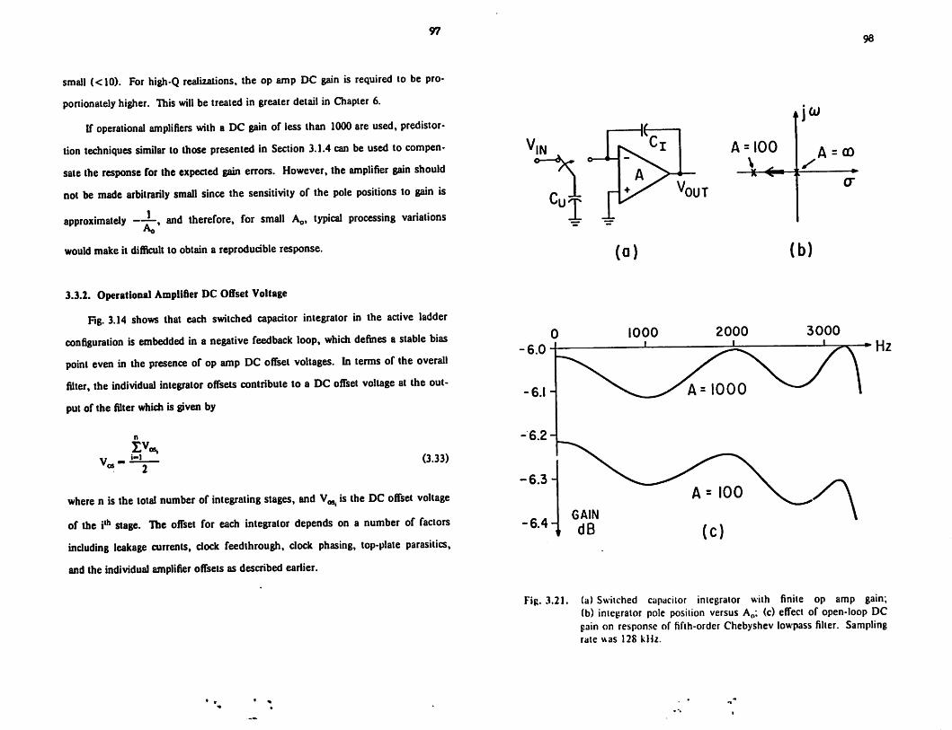
97
small (<10). For high-Q realizations, the op amp DC gain is required to be pro
portionately higher. This will be treated in greater detail in Chapter 6.
If operational amplifiers with a DC gain of less than 1000 are used, predistor
tion techniques similar to those presented in Section 3.1.4 can be used to compen
sate the response for the expected gain errors. However, the amplifier gain should
not be made arbitrarily small since the sensitivity of the pole positions to gain is
approximately ——, and therefore, for small A,,, typical processing variations
would make it difficult to obtain a reproducible response.
3.3.2. Operational Amplifier DC Offset Voltage
Fig. 3.14 shows that each switched capacitor integrator in the active ladder
configuration is embedded in a negative feedback loop, which defines a stable bias
point even in the presence of op amp DC offset voltages. In terms of the overall
filter, the individual integrator offsets contribute to a DC offset voltage at the out
put of the filter which is given by
v„-
2VCi-l (3.33)
where n is the total number of integrating stages, and V^ is the DC offset voltage
of the i* stage. The offset for each integrator depends on a number of factors
including leakage currents, clock feedthrough, clock phasing, top-plate parasitics,
and the individual amplifier offsets as described earlier.
A = 100
OUT
(a)
1000 2000j l
(A)
A = co/
(b)
3000L
98
-Hz
Fig. 3.21. (a) Switched capacitor integrator with finite op amp gain;(b) integrator pole position versus A(l; (c) effect of open-loop DCgain on response of fifth-order Chebyshev lowpass filler. Samplingrate was 128 kHz.

99
3.3.3. Common-Mode Range and CMRR
In switched capacitor integrators, the positive input terminal of the differential
amplifier is always connected to a DC bias voltage. Hence, there is no steady-state
common-mode input signal, and therefore the input common-mode range and
CMRR are not important parameters.
3.3.4. Amplifier Slew-Rate
The required op amp slew-rate performance is determined by several different
factors: (1) The maximum rate of change of the integrator output signal; (2) the
sampling frequency, (3) the duty cycle of the clocks, and (4) the clock phasing
which determines when the output is sampled. The switched capacitor integrator of
Fig. 3.22samples the input during d»] and integrates during <f>2 as shown in the tim
ing diagram. It will be assumed that Vout is sampled at the end of <f>2 (which
represents the worst-case) so that the total time available for slewing and settling is
t, where T-kdT depends on the duty cycle. Neglecting sampling for the moment,
the output signal can be represented as
^^ouift)-VpSin(o>t)
which has a maximum rate of change at o»0 of
dVom(t)|dl L op-
(3.34)
(3.35)
Therefore, the maximum change in the output during one clock period is depen
dent on the sampling frequency and is given by
K'L-"<oVpT--^ (3.36)
100
As shown in Fig. 3.22(b), the total available response time, t, consists of a slewing
time, tslew, and a settling time, tMl. Since the settling time is approximately con
stant, the allowable slewing time is
T
Hence, the required op amp slew-rate is
SRl$lew
"oVp
,_Js.T
(3.37)
(3.38)
where it is assumed that r>tset. For example, for a 3.4kHz signal with a 3 volt
peak, tuoVp=0.064 volts//isec. If kd-0.25 (25% duty cycle), and half of the
integration time is allowed for settling, —-0.5, then the required slew-rate is
0.51 volts//isec. The prototype filters to be described in Chapters 5 and 6 used an
NMOS operational amplifier with a measured slew-rate of 1 volt//isec.
3.3.r Anr.Aiiifier Settling Response
Consider a switched capacitor integrator which uses a two-pole amplifier witha
low frequency gain of Aqand a dominant pole at p,:
A(s)
1+-2-Pi
1+iP2
(3.39)
During the sampling interval, the capacitor C, stores theoutput voltage, and the op
amp is an open-loop condition. During the integration phase, the circuit can be
modelled as a charge multiplier responding to a step input. The transfer function

*J
+:
r0UT
101
i-^V(oVQUT
(°)
T
l^-r-H
J
/SLEWING TIME —H H"— t SLEW
SETTLING TIME —H
(b)
h- t SET
Fig. 3.22. (a) A switched capacitor integrator, and (b) the voltage waveformsdefining the slewing and settling times.
for the circuit of Fig. 3.23(a) is
H(s)1+
1 *
T(s)
where T(s) is the loop-gain of the charge multiplier,
T(s)-
C,A0
Cu+C,
1+_s_
Pi1+
_s_
P2
102
(3.40)
(3.41)
The step response of the circuit depends on the location of the closed-loop poles in
Eqn. (3.40) which are derived as
»1,2P1+P2 ±̂ [4p,P2(l+T0)-(p,+p2)2]l/2, (3.42)
where T0 is the low frequency loop-gain,
CAtrt0
Cu+C,(3.43)
A root-locus plot is shown in Fig. 3.23(b). The poles become complex when
T _ (P2~Pi>2 _ P20" 4p,p2 4p,'
(3.44)
which is typically about 500 for NMOS designs. Since the actual low-frequency
loop-gain is usually about 1000 (A0 ), the transient response will be complex. The
pole position, p2, is often dependent on loading, and therefore, the details of the
step response should be considered for the worst-case stage within the filter. In
general, settling time is the dominant consideration in determining the maximum

103
sampling frequency for a switched capadtor filter.
V,IN>
Cu
(a)
AP,P2
(b)
104
oVfJUT
Joj
-Pi
Fig. 3.23. (a) A model ofthe switched capacitor integrator during the integration lime; (b) root locus plot of the pole positions during theintegration time.

105
Chapter 4
DYNAMIC RANGE CONSIDERATIONS FOR SWITCHED CAPACITOR FILTERS
The dynamic range of a switched capacitor filter is defined as the ratio of the
RMS output voltage at a given total harmonic distortion (THD) level to the total
RMS noise voltage within a specified bandwidth. For example, in telephony appli
cations, the maximum signal level is 3 dB below the 1% THD signal level, and the
RMS noise voltage is measured in the c-message band which extends from 300 Hz
to 3.4 kHz.
The harmonic distortion generated by a switched capacitor integrator is deter
mined by the linearity of the operational amplifier, and by the peak signal level at
the output node of the integrator. The nonlinearity of the MOS capacitors also
contributes to distortion, but since the capacitor voltage coefficient is typically very
small (10 ppm/volt for metal over n*), THD is usually dominated by the opera
tional amplifiers.
There are two sources of noise in an MOS switched capacitor integrator:
(1) The noise of the MOS operational amplifier, and (2) the thermal noise gen
erated by the switches which form the switched capadtor resistors. The noise at
the output of a switched capadtor filter is determined by the RMS sum of the noise
contributions from each of the integrators. In this chapter, techniques are
presented for maximizing dynamic range while minimizing the silicon area require
ments.
106
4.1. Harmonic Distortion in a Switched Capacitor Integrator
The gain transfer curve of a typical NMOS operational amplifier is somewhat
nonlinear as shown in the enhancement-depletion example of Fig. 4.1(a). The op
ampnonlinearities give rise to harmonic distortion in a switched capadtor integrator
which depends on the peak output signal level. In this section, a method of analyz
ing low-level harmonic distortion in a switched capadtor integrator is presented.
The type-I inverting switched capacitor integrator of Fig. 4.1(b) is imple
mented with an MOS operational amplifier which has a DC open-loop gain of A
which is a function of the DC output voltage as shown in Fig. 4.1(a) and in Table I.
The z-pla". transfer function of this inverting integrator including gain effects is
given by
H(z) - -
A+l+-^Ci
(4.1)
- A+l
and bysetting z-e*"1, the magnitude of the integrator transfer function isobtained:
(hu)|A+l+-^ +[A+l]2-2[A+l] A+l+-^- T17T-
cos(o)T)
(4.2)
An analytical evaluation of harmonic distortion based on Eqn. (4.2) is quite compli
cated. Fortunately, THD can be estimated by using the concept of differential gain
error which involves calculation of the relative gain change at a given output vol
tage with respect to the gain at a quiescent output voltage (65). The positive
differential gain error is defined as
E*-°^52 (4.3)

(a)
V,INo 6>"V*- O——O
QUI
(b)
-i 6 VOLTS
'DD -
o vss =
BB
-6
107
7.5
7.5
-12.5
ov0UT
Fig. 4.1. (a) Open-loop gain transfer characteristic for the enhancement-depletion NMOS op amp of Chapter 5; (b) A type-I invertingswitched capacitor integrator where the op amp has the gain characteristic given in (a).
108
v0UT SMALL SIGNAL INTEGRATOR
(VOLTS) GAIN GAIN AT fo
5.0 122 0.99282
4.5 172 0.99537
4.0 273 0.99768
3.5 628 0.99910
3.0 983 1.00053
2.5 971 1.00052
2.0 958 1.00051
1.5 946 1.00049
1.0 932 1.00047
0.5 919 1.00046'
0.0 906 1.00044
- 0.5 864 1.00038
- 1.0 822 1.00032
- 1.5 786 1.00026
- 2.0 753 1.00020
- 2.5 505 0.99950
- 3.0 252 0.99736
- 3.5 165 0.99511
- 4.0 123 0.99289
- 4.5 80 0.9882*5
- 5.0 46 0.97847
Table I. The op amp open-loop gain, and the integrator gain as a function ofthe output voltage level.

109
and similarly, the negative differential is
E--G^Go.(4.4)
where for this example, GQ is the integrator gain at zero volts output, and G"*" and
G~ are the integrator gains at the maximum positive and negative excursions of the
output signal, respectively. The second and third harmonic distortion terms are cal
culated by using the following equations:
and
HD2 - I(E+-E")
HD3 - r7(E*+E-).24
(4.5)
(4.6)
These equations are valid at small distortion levels where HD2 is proportional to
the output signal, and HD3 is proportional to the square of the output signal.
The distortion performance of the switched capacitor integrator of Fig. 4.1(b)
at f0-3.2 kHz with a 128 kHz sampling rate has been calculated using the method
described above. The integrator gain at f0 (which is ideally one) was calculated
using Eqn. (4.2) with the results shown in Table I, and then using Eqns. (4.3) thru
(4.6), the second and third harmonic distortion terms were calculated as shown in
Fig. 4.2. When the peak output approaches 4.0 volts, the harmonic distortion
increases significantly so that the differential analysis described above can no longer
be used. Fig. 4.2 is in good agreement with the experimental results presented in
Chapter 5 which show a dramatic increase in distortion for a similar peak voltage.
110
<UJQ_
>
h
o
CO
QV X
©
CO
_©"c4
HARMONIC DISTORTION(dB)
•
*-•
< | | i •^ 1 1 1 1
o O o o o
1 1
CO
1 1
o
1
Fig. 4.2. Second and third harmonic distortion for the switched capacitorintegrator using the op amp characteristic of Fig. 4.1.

Ill
4.2. Scaling Techniques for Switched Capacitor Filters
The dynamic range of a switched capacitor filter with more than one integra
tion stage is maximized by scaling the circuit so that the peak output voltage levels
are the same for each of the integrators [66]. Several different scaling techniques
are presented in this section along with a brief discussion of the basic noise-
distortion-silicon area tradeoffs.
4.2.1. Impedance Scaling
An RLC prototype circuit is impedance scaled by a factor of k using the fol
lowing relationships [43]:
and
Ri — kRj
Lj-kLj
Cm-
(4.7a)
(4.7b)
(4.7c)
The effect of impedance scaling is illustrated by considering the second-order RLC
prototype shown in Fig. 4.3(a). The current flowing in this circuit before scaling is
I(s)sC
s2LC+sRC+lVin(s)
and the output voltage is given by
1VOUI(s) -s2LC+sRC+l
Vin(s).
(4.8a)
(4.8b)
The scaled version of this circuit obtained using Eqn. (4.7) is shown in Fig. 4.3(b).
The value of the current flowing in this circuit is found by substituting the scaled
112
(a)
k VOUT
(b)
Fig. 4.3. A singly-terminated second-order RLC filter (a) before and(b) after impedance scaling.

element values into Eqn. (4.8a) to obtain
-f sCI(s)
s2kL ShHIfVin(s) - f
+ 1k s2LC+sRC+l
V,„(s)
and similarly, the output voltage is obtained from Eqn. (4.8b) as
Vin(s) Vin(s)VOUI(s)
'!M[f]~M[£ +1s2LC+sRC+l
113
(4.9a)
(4.9b)
It is apparent from Eqns. (4.8) and (4.9) that impedance scaling reduces the current
by a factor of k while the voltage level is unchanged. In a similar manner, all
inductor currents in a high-order filter are reduced by a factor of k due to
impedance scaling while all capadtor voltages remain unchanged.
The dynamic range is maximized by scaling the filter so that all internal
integrator outputs have the same peak amplitude [17],[66], A switched capacitor
implementation of the scaled circuit of Fig. 4.3(b) has one output voltage which is
directly proportional to the inductor current, I (bandpass output), and another out
put which is equal to the capacitor voltage, Vou, (lowpass output). For Q»l, the
maximum lowpass output voltage for the circuit of Fig. 4.3(b) occurs at the fre
quency «0-[LCrl/2 and is
(max) -1
1/2
and the maximum bandpass voltage, Vou„ corresponding to I is
V QUI # .. v 1"VT(maX> " kR
(4.10a)
(4.10b)
114
In order for the magnitudes of Eqns. (4.10a) and (4.10b) to be equal, the circuit
1/2
must be impedance scaled by a factor of k—
A., estimate of the silicon area required to implement a switched capacitor ver
sion of the scaled RLC prototype of Fig. 4.3(b) can be made by assuming that the
area is dominated by the integrating capacitors for the L and C stages. The total
area required is proportional to the capacitance ratio
Area a —^ —C„
fc kL+£k
(4.11)
where L and C are the normalized element values for a cutoff frequency of
1 rad/sec and coco is the desired cutoff frequency. The area of Eqn. (4.11) is
minimized for a scaling factor of
1/2
(4.12)
Notice that for this example, the scaling factor which optimizes dynamic range also
minimizes the silicon area required. For high-order filters, it is generally true that
those conditions which maximize dynamic range also minimize the required die
area.
The impedance scaling technique described above simultaneously reduces all
inductor currents by k. Unfortunately, for high-order filters, the peak inductor
currents are generally not equal before scaling, and therefore after scaling, the peak
amplitudes will still be different since all currents are equally affected. Thus,
although impedance scaling works well for second-order filters, it is not generally
applicable for optimizing dynamic range in high-order filters. A switched capacitor
scaling technique which can be used to independently scale all internal nodes
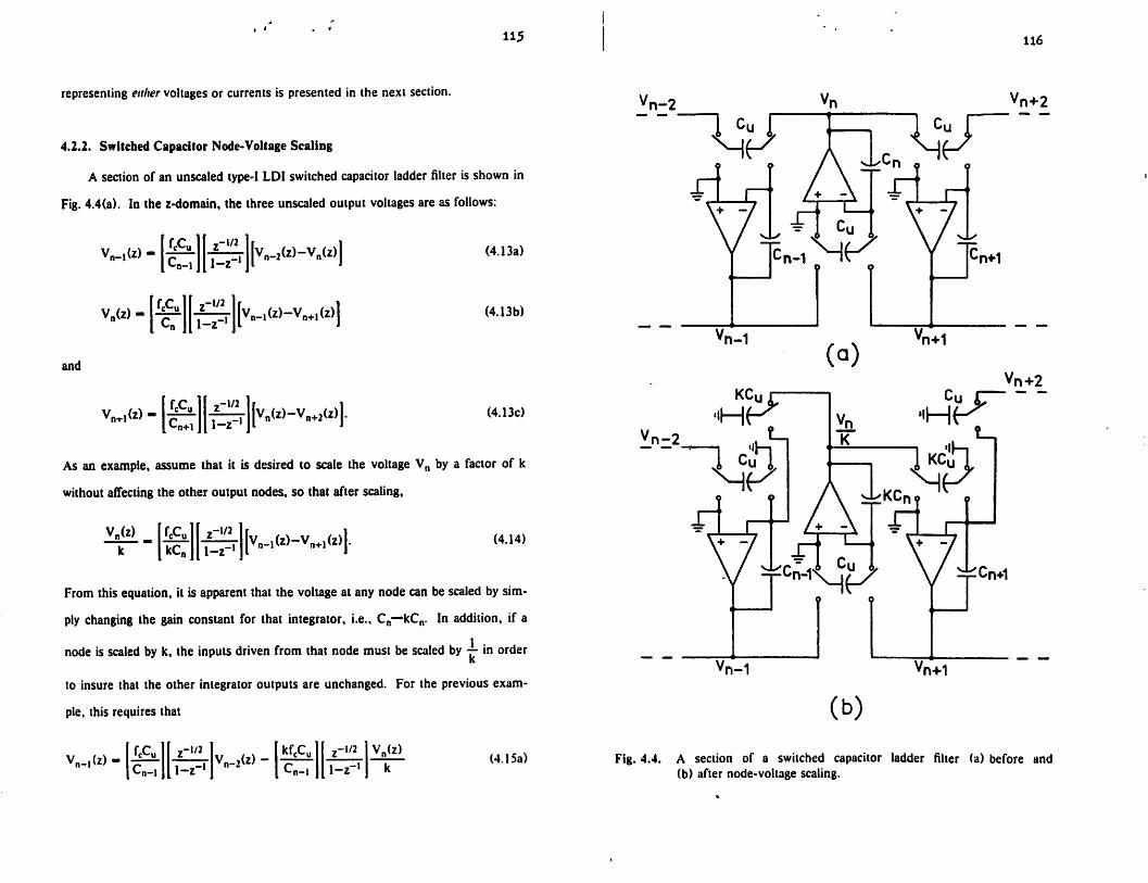
U5
representing either voltages or currents is presented in the next section.
4.2.2. Switched Capacitor Node-Voltage Scaling
A section of an unsealed type-I LDI switched capacitor ladder filter is shown in
Fig. 4.4(a). In the z-domain, the three unsealed output voltages areas follows:
^]K,<Z>-Vn+l<
(4.13a)
Vn(z) - (4.13b)
and
V„.,(z) -f C
'n+l
f^r][vn(z)-vn+2(z)]. (4.13c)
As an example, assume that it is desired to scale the voltage Vn by a factor of k
without affecting the other output nodes, so that after scaling,
VB(z) £ll#|M-~H (4.14)
From this equation, it is apparent that the voltage at any node can be scaled by sim
ply changing the gain constant for that integrator, i.e., Cn-*kCn. In addition, if a
node is scaled by k, the inputs driven from that node must be scaled by — in order
to insure that the other integrator outputs are unchanged. For the previous exam
ple, this requires that
v„-,fc>-f«c„| z-,/2 Vn.2(z) -
kfcCu ,-1/2 |cn_, .»-*"'. |c„_, l"2"1 1
VB(Z)(4.15a)
116
Vn-2 Vn+2
Vn+2
Vn-1 Vn+1
(b)
Fig. 4.4. A section of a switched capacitor ladder filter (a) before and(b) after node-voltage scaling.

and
Vn+1(z)kfcCu 2-l/2 V„(z) [ftCu
Cn+t
z-l/2 1on+J 1-z-' k 1-z"1
117
(z).n+2 (4.15b)
Eqn. (4.15) shows that all of the switched capacitors driven from a scaled node,
Vn(z)—-—. are changed to a value of kCu. For example, if a node voltage is
halved (k—2), then all switched capacitors connected to that node are doubled.
The switched capacitor section after node-voltage scaling is shown in Fig. 4.4(b). In
general, two additional switched capacitors are added for each scaled node, and if k
is not an integer, the capacitor matching accuracy between the different sized
switched capacitors is slightly reduced.
For both node-voltage scaling and impedance scaling, there is a tradeoff
between noise and signal level (distortion). This tradeoff is illustrated by assuming
that the gain from the input to the output of the filter is constant. For an arbitrary
internal node, Vx, the following relationships apply for the unsealed and scaled ver
sions, respectively:
and
vVOUI fvx|v„ K.
vVOUl
vx
k kvou, 1 vx 1
k
vto 1 V* ,|kVm
(4.16a)
(4.16b)
The first term in both equations is a measure of the noise gain from Vx to the out
put of the filter, and the second term represents the magnitude of the peak signal at
118
node Vx relative to the input. Hence, the first term determines the noise perfor
mance, and the second term determines the distortion performance. Notice from
Eqn. (4.16b), that as the noise gain is increased by k, the peak amplitude at Vx is
reduced by k and vice-versa. Thus, there is a direct tradeoff between noise and dis
tortion, and it is for this reason that the peak amplitudes are set equal for all stages
in order to maximize dynamic range.
4.2.3. Switched Capacitor Loop Scaling
For bandpass and bandreject RLC filters, the relative spread in the LC ele
ment values rapidly increases as the seleaivity increases. For example, consider
the RL lowpass prototype shown in Fig. 4.5(a). Applying the lowpass-to-bandpass
transformation of Chapter 2 results in the circuit of Fig. 4.5(b) where the bandpass
reactive values are given as
and
QLn0>n
Cn-QLnw0'
(4.17a)
(4.17b)
From these equations, it is apparent that the ratio of -~ increases in proportion toCB
Q2 which is very undesirable because in a switched capacitor implementation, it
results in a similar spread in the required capacitor ratios. In addition, if this net
work is not scaled, the peak current remains constant for a fixed termination resis
tance while the peak capacitor voltage increases in proportion to Q. Thus, the
dynamic range is significantly degraded for high-Q applications.

R•AA/W-
(a)
R•WW-
(b)
119
n
LD=QLn
B D,
icB= QOnLo"-n
Fig. 4.5. (a) Asingle-pole RL filter, and (b) a bandpass circuit obtained usingthe lowpass-to-bandpass transformation.
120
A signal flowgraph for the RLC bandpass prototype of Fig. 4.5(b) is shown in
Fig. 4.6(a). The current, I,, is given by
I,- ^M-1 (4.18a)
which can also be written as
Il"T QLn QLn QLn (4.18b)
Thus, all inputs to the Ii integrator have been divided by QLn and the integrator
gain constant has been changed to &>0. Similarly, the lowpass output voltage, V2, is
written as
V,-Q"oLr
I. (4.19a)
or equivalent^,
*M- (4.19b)
Thus, the input of the second integrator has been multiplied by QLn, and the gain
constant has become w0. Using Eqns. (4.18) and (4.19), an equivalent signal
flowgraph is drawn in Fig. 4.6(b). At this point, the drcuit has been rearranged so
that the integrator gain constants are equal. However, for maximum dynamic
range, the peak amplitudes must still be scaled to be equal. From Eqn. (4.10a), the
maximum lowpass output voltage is found to be
V2(max) - I1/2
QLnR
and the maximum bandpass current is
(4.20a)
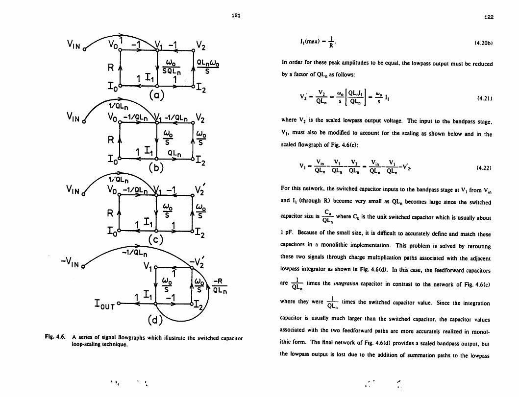
121
1 -1/QLn V?
^UT0
Fig. 4.6. A series of signal flowgraphs which illustrate the switched capacitorloop-scaling technique.
122
I,(max) - tj-. (4.20b)
In order for these peak amplitudes to be equal, the lowpass output must be reduced
by a factor of QLn as follows:
QL„QL„I,QL„ ^ (4.21)
where V2 is the scaled lowpass output voltage. The input to the bandpass stage,
V,, must also be modified to account for the scaling as shown below and in the
scaled flowgraph of Fig. 4.6(c):
V, - Ji--.lL-Ji. - Jk_J^-v"1 QLn QLn QLn QLn QL0 V* (4.22)
For this network, the switched capacitor inputs to the bandpass stage at V, from V,
and I, (through R) become very small as QL„ becomes large since the switched
. . Cucapacitor size is —— where Cu is the unit switched capacitor which is usually about
v*-n
1 pF. Because of the small size, it is difficult to accurately define and match these
capacitors in a monolithic implementation. This problem is solved by rerouting
these two signals through charge multiplication paths associated with the adjacent
lowpass integrator as shown in Fig. 4.6(d). In this case, the feedforward capacitors
are qTJ- »mes the integration capacitor in contrast to the network of Fig. 4.6(c)
where they were •—- times the switched capacitor value. Since the integration
capacitor is usually much larger than the switched capacitor, the capacitor values
associated with the two feedforward paths are more accurately realized in monol
ithic form. The final network of Fig. 4.6(d) provides a scaled bandpass output, but
the lowpass output is lost due to the addition of summation paths to the lowpass

123
stage. This technique has been verified by other workers for monolithic versions of
second-order [52] and high-order [67] bandpass and bandreject filters. The area-
noise-distortion considerations are identical to those of the impedance and node-
voltage scaled networks.
4.3. Noise in a Switched Capacitor Integrator
In this section, the sources of electrical noise in a switched capacitor integrator
will be described.
The equivalent input noise spectral density of an MOS operational amplifier is
frequency dependent as illustrated in Fig. 4.7(a). The power spectral density at low
frequendes (<10 kHz) is dominated by the flicker component which decreases as
—, and the spectral density at higher frequendes is relatively constant (typically
100 nV/|Hz|1/2) and is determined by the thermal noise associated with the channel resistance of the MOS transistors. Depending on the passband frequendes of
the filter, one or both of these components may be important in determining the
dynamic range at the output of the filter.
The noise performance of the Miller integrator of Fig. 4.7(b) will first be
analyzed considering both the thermal noise of the resistor and the equivalent input
noiseof the operational amplifier. It will be assumed that the op amp hasa low fre
quency gain of A0with a one-pole rolloff to the unity-gain frequency, fu. The gain
1constant of the integrator is f0
HR(01+
JfA0
as shown in Fig. 4.8(a).2wReqCj
First, consider the spectral noise contribution from the resistor. As shown in
Fig. 4.8(a), this white noise source is lowpass filtered by the integrator which has a
transfer function of
(4.23)
124
BROADBAND NOISE
1MHZ
Ofc>
(b)
Fig. 4.7. (a) A typical plot of the equivalent input noise power spectral density for an NMOS depletion-load op amp; (b) A Miller integratorwith op amp and resistor noise sources.

125
OPEN-LOOP
OP AMP
-H 1 ^1 I I V **10 100 1K 10K 100 K IM^OMHZ
(b)
Fig. 4.8. (a) Transfer function from the resistor noise source to the output;(b) the transfer function from the op amp equivalent noise sourceto the output.
The power spectral density at the integrator output is therefore equal to
VWesuro^ " [4kTREQ]A 2
1+fA0
1fo |2
126
(4.24)
Now, consider the noise contributed at the integrator output by the opera
tional amplifier. The transfer function from V2;(0 to the integrator output of
Fig. 4.7(b) is given by
. 1-hCjReqsCiR
(4.25)1REQ
and is shown as the darkest line in Fig. 4.8(b). Notice that this curve is made up of
four separate sections, and therefore, the output power spearal density can be
determined separately for each of the four cases as follows:
and
V2OU,(0 - V2i(OA02 for 0<f<-2-A„
V2out(0 - V2i(f) for -2-<f<fn
V2ou,(0 - V2,(0 for f0<f<fu
V20U,(f) - V2i(f)f
for f„^f
(4.26a)
(4.26b)
(4.26c)
(4.26d)
where V2,(f) is the equivalent input noise power spectral density of the operational
amplifier. Given an op amp power spectral density, Eqn. (4.26) can be evaluated to
determine the total RMS noise at the integrator output in any specified bandwidth.

127
Next, consider the spectral density at the output of the switched capacitor
integrator of Fig. 4.9(a) due to the equivalent input op amp noise. For baseband
frequencies, the switched capcitor is equivalent to a resistor, REQ, and therefore,
for these low frequencies, the switched capacitor integrator is identical to the Miller
integrator of Fig. 4.7(b). Thus, a similar analysis applies with a slight change in the
frequency limits as follows:
and
V2OU,(0 - V2i(OA02 for 0<f< Js.Aft
V2OU,(0 - V2S(0 for -^-<f<f0An
V2out(« - V2i(f) forf0<f<|-
(4.27a)
(4.27b)
(4.27c)
assuming y<fu where fc is the switched capacitor sampling frequency. The op
famp noise above y in frequency must be treated using sampled-data techniques.
It will be assumed that fc is greater than the -jr noise corner of the op amp so that
flicker noise is notaliased and thus, only the broadband opamp noise need be con
sidered. The output noise for this case depends on when the output is sampled.
For example, if the output is sampled during #, as in Fig. 4.9(b), the op amp is in
unity gain as shown in Fig. 4.10(a), and the squared RMS noise at the output is
V2OUTu
ao
-/VBB3 l+(f)2to
-1
dfwLV,uvBB
(4.28)
where VBB2 is the broadband power spectral density. The sampled output power
v,IN«>
V,AkTRs R
No—(^)--VWVr-f O O *
w OPEN ^t^ERs ^S"No o o f-£)AAA/U-
Cy ^r\
(0
128
i-<v(OUT
1-^V,ov0UT
OUT
Fig. 4.9. (a) A switched capacitor integrator; (b) the noise model during </»,and (c) the noise model during 4>2.

129
OMHZ
(a)
('♦3>
10 100 OMHZ
Fig. 4.10. Frequency response from the op amp input noise source to theintegrator output for (a) the circuit of Fig. 4.9(b) and (b) for thecircuit of Fig. 4.9(c).
130
spectral density is therefore
irfuVuvBB'PSD
2fc(4.29)
On the other hand, if the output is sampled during 02 as in Fig. 4.9(c), the closed
Cloop op amp gain is (1+tt-) as shown in Fig. 4.10(b). The squared RMS noise at
ci
the output for this case is
V 2vout
CO VBB2(1+-^-)2
l+(f)2(l+>)2df
TfuU+T^VBB2
and the corresponding power spectral density is
'PSD
wfu(l+7^)VBB2M
2f.
Equations (4.28) through (4.31) assume that fu is less than
(4.30)
(4.31)
1
2irR<CIf this
assumption is not valid, the same analysis can be used with fu replaced by _
The noise contributions from the MOSFET switch transistors also need to be
considered. Again, the baseband and high frequency terms will be considered
separately. The transistor M( connected to 0, has an on resistance of R, as shown
in Fig. 4.9(b). For low frequencies, the switched capacitor can be replaced by a
resistor, REq, and the Miller integrator of Fig. 4.7(b) along with the transfer func
tion of Fig. 4.8(a) are used to obtain the spectral densities at the integrator output:
Voul2 - 4kTR,A02 for0<f<-2- (4.32a)

131
and
V0Ul2-4kTRs|^|2 *>r£<f. (4.32b)
The total squared RMS noise contribution at the integrator output from this noise
source is
V2rms " 2kTirRsA0f0. (4-33)
At low frequendes, transistor M2 connected to *2 also has its noise filtered by theintegrator so that Eqns. (4.32) and (4.33) also apply for the noise source of thattransistor.
Finally, the sampling effects for these two noise sources must be considered.When M, is on, as in Fig. 4.9(b), its noise is lowpass filtered by the RSCU combination giving atotal squared RMS noise on Cu of
kTv RMS " ~ •
(4.34)
When M, is opened, this noise is sampled onto Cu giving apower spectral density
at Cu of
w2 kT . kTR rt (4.35)V2psd " TfT kTREQ-
The transfer function from Cu to the integrator output is derived from the circuit of
Fig. 4.9(c) to be
H(s)
Ss.c,
l+sR,Cu(4.36)
132
and the output spectral density is therefore
kTR
V2 (0 -
EQ(4.37)
[l+(27rfRsCu)2]
When M2 is on, its noise is filtered onto Cu in asimilar manner, and when M2 issubsequently opened, this noise is sampled onto Cu. However, +, then turns onM„ and this noise voltage is returned to the input source so that M2 does not contribute any sampled noise at the integrator output.
The spectral density calculations for the switched capadtor integrator can beused to estimate the noise performance of any switched capacitor filter by multiplying the power spectral density by \[(()\ where T(f) is the transfer function fromthe integrator output to the filter output, and then integrating over the desired
bandwidth.

133
Chapter 5
EXPERIMENTAL RESULTS FOR NMOS LOWPASS PROTOTYPES
In this chapter, experimental results from two NMOS integrated switched
capadtor ladder filters are presented. The first design realized a fifth-order Che
byshev lowpass response, and the second, a third-order Cauer lowpass
response 124]-[25]. Monolithic MOS capadtor ratios and dock frequency were used
as the predsion components. The performance of the NMOS depletion-load opera
tional amplifier used to implement the filters is also given.
5.1. NMOS Depletion-Load Operational Amplifier
The NMOS operational amplifier used in both filter designs (shown schemati
cally in Fig. 5.1), is a simplified version of a recently reported design [14]. It was
integrated using the NMOS metal-gate depletion-load process given in Appendix I.
The measured results presented in Table I are in good agreement with the theoreti
cal calculations of Appendix 2.
5.1.1. DC Open-Loop Gain
The DC open-loop gain of NMOS depletion-load operational amplifiers
depends on both power supply and body-bias voltages [14], [47]. Figure 5.2 shows
that the measured open-loop gain for ±7.5 volt supplies with 0, 2.5, and 5.0 volts
of body bias varied from 400 to 1000 as measured about zero volts at the output.
Figure 5.3 shows the low frequency open-loop gain characteristics for ±5.0 volt
supplies with 0, 2.5 and 5.0 volts body bias, and in this case, the gain ranged from
33 to 60. As discussed in Chapters 3 and 4, for lowpass filters, it is desirable to
have a small-signal voltage gain of several hundred over the entire output voltage
range in order to minimize frequency response errors and harmonic distortion.
I-3
13!f
cmIcn p° cojooco|d
1-Ul
too2
z
o
h-Ul-JQ_
UJo
J_
(/)
h-_J
O>
If)•
i
> ii
(7)
r-
Ld
Li_
(/)o
i_J
0
0
J"
u
c
J
olco^Id
5
r-
LA
O-
CD
II
Q_
oo
O
CNCM
cm*-^
Z
UJ
2L
5JcO
UJu
z
dO
<XzUI
TL
J- __T~L ^
«<r cm
o ^ d ^iOlcO
o|o-1 *- _j
2
to
UI1rL
1J
rL J
do
<
i£> CO
od
S EVICESIZ
L J
Jr
LJ
r-
_lO>
•xt
d
. L H Q_J —
O>
CvJ
T
CM
10.010.0 0.80.8
•
1^-x*|coHo
tii U
I Z>
ii
CO
Fig. 5.1. Dcplciion-load NMOS operational amplifier.
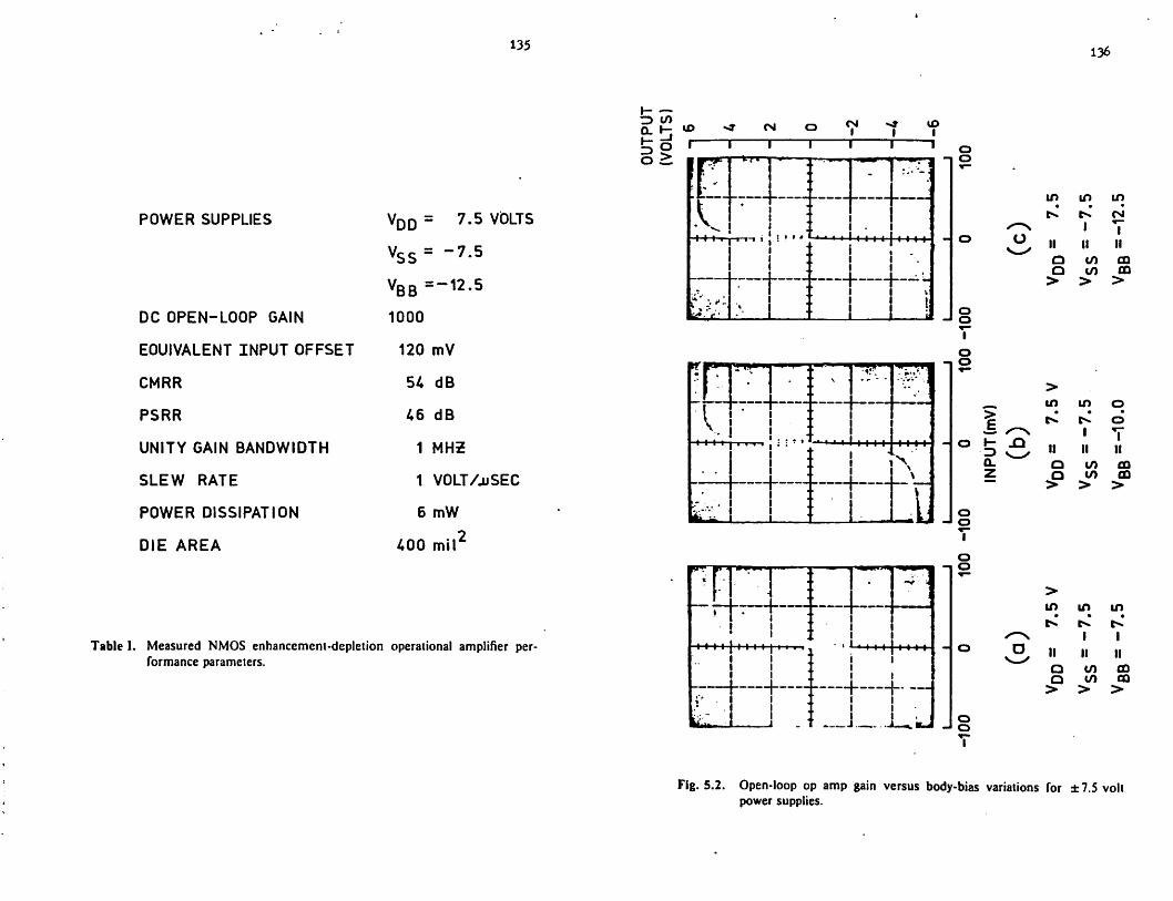
POWER SUPPLIES
DC OPEN-LOOP GAIN
EOUIVALENT INPUT OFFSET
CMRR
PSRR
UNITY GAIN BANDWIDTH
SLEW RATE
POWER DISSIPATION
DIE AREA
135
VDD = 7.5 VOLTS
VSS= ~7'5
VBB=-T2.5
1000
120 mV
54 dB
A6 dB
1 MHZ
1 VOLT/juSEC
6 mW
400 mil2
Table I. Measured NMOS enhancement-depletion operational amplifier performance parameters.
I- —
O^
ID *4" CM
i 1 r
V I *•'* 1 """
I
O CM <** ID» I I
"1 1 1
I
oo
•i ii i i
II
-*-1 < ' I I I I I | I I I I - o o
•a»-'V-
iL*.
r^
rMM
•t"
'j \*» •< ^"T
I I
i i
iLA
1.'.f^f^W
' • • - .II
•*•» » I I I I I I
I I 1 \
—!—;r—I—r-\ni_J_L
ii
-+•i
ij
iii
. L
u. • wimi
I I
I I
J_.l
oo
oo
>E ^
o i- .q
oo
OO
oo
136
in in in•
tv t^ CM
I 1
II ll II
O to COQ i/> CD
> > >
>
in
II
in
I
ll
o
dTll
a to coQ 10 00
> > >
>
in in m• • •
r» t»» t«*
1 1
ll ll II
Q to CDO to CO
> > >
Fig. 5.2. Open-loop op amp gain versus body-bias variations for ±7.5 voltpower supplies.

3C0
^> r
.U+H-H-HH
CM *-
lllllllll
&-*«•..
•r- CM
T 1 1• • i>W • • ••' I
I I M | I I MI<
._L .
«L
c I'll I i
Mill. •Ml I M I M M
1 i I ! i t
....,• J
i J I iv ;J I I I L. ^
M M | II i
III
-J.
MM I ♦ M
OO
oo
o-i o
o
>J: ^
o I- .Q
Q_
oo
Oo
oo
I
137
o o o
in in o
11
II ll II
O C/> COQ to CO
> > >
>
o
in
ll
oa
>
in
I
ll
in
I
II
tO CDCO CO
> >
>
o
in
o
in
1
o
in
1
ll ll ll
ao
>
toto
>
CD
CO>
Fig. 5.3. Open-loop op amp gain versus body-bias variations for ±5.0 voltpower supplies.
138
Hence, for best filter performance, this particular amplifier should be operated with
±7.5 supplies with 5.0 volts body bias. Note from Fig. 5.2 that when the output
voltage is below -3.2 volts, the gain decreases to about 100. This point on the gain
curve corresponds to the voltage where a sharp increase in harmonic distortion is
observed in the filter.
5.1.2. Equivalent Input Offset Voltage
The measured offset voltage of 122 mV in Fig. 5.4 is typical of this amplifier,
and is primarily due to the paraphase input stage. As described in Chapter 3, the
amplifier offset voltages contribute to a DC offset voltage at the filter output which
should be minimized in order to maximize dynamic range. The offset voltage of
this particular amplifier can be decreased by unbalancing the input pair of transis
tors in order to counteract the effect of unequal loads.
5.1.3. Common-Mode Range and CMRR
The measured common-mode range and CMRR are displayed in Fig. 5.5.
This parameter is not important for switched capadtor integrators if the op amps
are used with the noninverting input connected to a DCbias voltage since there are
no steady-state common-mode signals for this case.
5.1.4. Equivalent Input Noise
The measured unity-gain noise spectral density is shown in Fig. 5.6. The
measured j noise corner is at about 10 kHz, and the broadband noise spectral
density at 2 kHz is about 1 /*V/[Hz],/2.

OUTPUT (VOLTS)6r
-2
-4
-6
-150
DIFFERENTIAL INPUT (mV)
VDD= 7.5 V
VSS= ~7-5
VBp=-12.5Vos = 122 mV
Fig. 5.4. Op amp input offset voltage.
139
COMMONMODE
INPUT(VOLTS)
6 r
-A
~6 L
-150
INPUT OFFSET (mV)
VDD= 7.5 V
vss=-7-5
VBB =-12.5
CMRR = 54 dB
140
Fig. 5.5. Measured op amp common-mode range and CMRR.
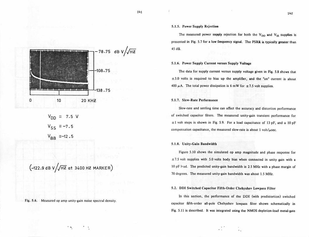
1M
-78.75 dBv//HZ
-108.75
-138.75
10 20 KH2
VDD = 7.5 V
Vss =-7.5
VBB =-12.5
(-122.9 dB VA/hI at 3400 HZ MARKER)
Fig. 5.6. Measured op amp unity-gain noise spectral density.
> " >
142
5.1.5. Power Supply Rejection
The measured power supply rejection for both the VDD and V^ supplies is
presented in Fig. 5.7 for a low frequency signal. The PSRR is typically greater than
45 dB.
5.1.6. Power Supply Current versus Supply Voltage
The data for supply current versus supply voltage given in Fig. 5.8 shows that
±3.0 volts is required to bias up the amplifier, and the "on" current is about
400 fiA. The total power dissipation is 6 mW for ±7.5 volt supplies.
5.1.7. Slew-Rate Performance
Slew-rate and settling time can affect the accuracy and distortion performance
of switched capacitor filters. The measured unity-gain transient performance for
±1 volt steps is shown in Fig. 5.9. For a load capacitance of 13 pF, and a 10 pF
compensation capacitance, the measured slew-rate is about 1 volt//iSec.
5.1.8. Unity-Gain Bandwidth
Figure 5.10 shows the simulated op amp magnitude and phase response for
±7.5 volt supplies with 5.0 volts body bias when connected in unity gain with a
10 pF load. The predicted unity-gain bandwidth is 2.5 MHz with a phase margin of
70 degrees. The measured unity-gain bandwidth was about 1.5 MHz.
5.2. DDI Switched Capacitor Fifth-Order Chebyshev Lowpass Filter
In this section, the performance of the DDI (with predistortion) switched
capacitor fifth-order all-pole Chebyshev lowpass filter shown schematically in
Fig. 5.11 is described. It was integrated using the NMOS depletion-load metal-gate

143
^trjTj' j,t:TTT^]TT
VERT.2V/DIV
H0R.50 mV/DIV
VDD= 7.5V
VBB=-12.5
+ PSRR =46 dB
*••
^T4++-f MM •H-+4 H 4 I MM
& al2 aafci j^ a.Av;
Co)
Fig. 5.7. Measured op amp PSRR.
rfcfil idi
— VERT. 2V/DIV
HOR. 50 mV/ DIV
VDD= 7.5V
vSs=-7-5
VBB=-12.5
- -PSRR = 54 dB
TOTAL SUPPLY CURRENT
600
400
200
0
-200
-400
-600
-6-4-2 0 2 4 6vss vDD
Fig. 5.8. Op amp supply current versus power supply voltage.INPUT/OUTPUT
(1V0LT/DIV)
.beqebq•BBOGnn
„ rrnnouu
INPUT/OUTPUT(1V0LT/DIV)
I 1—I 1 I L_J
i>S/DIV .,
r \ DD=(a)
HRscaa
i—i—i—i—i i i
5.0 V -^/D'VVSS= -5.0 (b)VBB=-10.0
CL = 13 pF
CC = 10 pF
Y\f,. 5.9. Measured op amp slew-rale performance.
M

,J==ifno
Lin
o'A
•s\
/6
i»
1f'o
t
•:Z
1i
^-"
':
!i£j?;5—
nn
iT
rr
t«
»-v:
I•
i"IK
.CI
•.-*
^r
L»—•"*""
"1
U".!
-IM—
2t4
t*»
0*
1
>*.jp
J•
U-.:w
*-io
»Jl.>
-.
.0«
.«il'i
IJI
alll-I1
-3
.(-,.>
•1
•ttl.v
••
y^
y*»
**m
e\•
J.i.Jtri—
.(.l.vli-l
-m
iii«
-.
;ci
<<
t;-<
••
/•ll
J•
IC.tl.fl-.
—n
rrn
rr
id
in
ci
il>.*
*«
*-t
—5
»»
j-rrT
»t.»
tIf
.I>
».l<
>-.
••
u«
.-.»
-i
—m
-jrtm
r«
>•
-..{-I
il.
j$
:•
I♦»
•l»
..M
jf
:>
|—
"m
i.
..<
i—
•fit.;t.«
*
ia
>;.
»>
-t
in
.C
I.-.
Kiltl
l>>
:.Ii.<
••>
•€
iO
.•<
.••«
.J.,4
l;-<
::
/^:
•..•.....•!
•.'.
•>
..1
*1
lj>*
;..<
*i
(«
••••••
1
•..l,..i'l
•iv
...i
•«
••
'tv<
-.:.<
-1
<i.>
i.i-i
:/
•-••-
S5
TS
T7
TT
•ii»
»...i.-l
4W
<V
••-
1
I
..•..i.-i
•......I.-I
•{.(.it.*
!
-»
o»
«o
wr
IV
-..
»»
-i
IC
.V
II
•••
Iw
l.S
I.'
.
\r
*•"«
i•
•—
irrru
rr
IV*
t.
••-.*I3
«.J|
;•«
•U
...1I-
1
:•
.'.I
••.'!
•.)•
»l.-l
•«
.»
..l.-|
—•'—
•—
—•
—T
brjiir*
-!—
•;«
-i
•«
.•
,U
-«
„,_
.,,*
w»
..l.'l__
iliTllI*
!
-ten
-v
—T
ii*
...
<-
•i*
.|*
or-
I
::
—
:.
..
_3
31
jX
tC
-T
If
.I..-.
>(•
..'/i-w
-T
TIT
TR
TIL
l.,.1
-1
Ui
t.i.'l
M«M
M~C
*1
04•••••(
tt«
tO
Ot-l
:.:0».B
0«0*I
to*
Ml
...
...;t_
,,..,—
••"
~T»«tO
>«-|-
—---
*•!
"»
•-!•••••......
4}
T3oQQ00
o.
ECO
aoEcs"i
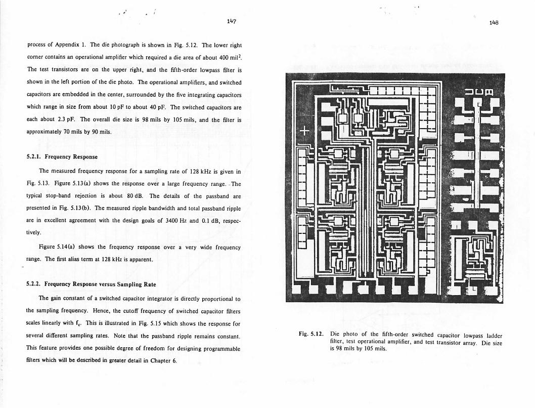
147
process of Appendix 1. The die photograph is shown in Fig. 5.12. The lower right
corner contains an operational amplifier which required a die area of about 400 mil2.
The test transistors are on the upper right, and the fifth-order lowpass filter is
shown in the left portion of the die photo. The operational amplifiers, and switched
capacitors are embedded in the center, surrounded by the five integrating capacitors
which range in size from about 10 pF to about 40 pF. The switched capadtors are
each about 2.3 pF. The overall die size is 98 mils by 105 mils, and the filter is
approximately 70 mils by 90 mils.
5.2.1. Frequency Response
The measured frequency response for a sampling rate of 128 kHz is given in
Fig. 5.13. Figure 5.13(a) shows the response over a large frequency range. The
typical stop-band rejection is about 80 dB. The details of the passband are
presented in Fig. 5.13(b). The measured ripple bandwidth and total passband ripple
are in excellent agreement with the design goals of 3400 Hz and 0.1 dB, respec
tively.
Figure 5.14(a) shows the frequency response over a very wide frequency
range. The first alias term at 128 kHz is apparent.
5.2.2. Frequency Response versus Sampling Rate
The gain constant of a switched capacitor integrator is directly proportional to
the sampling frequency. Hence, the cutoff frequency of switched capacitor filters
scales linearly with fc. This is illustrated in Fig. 5.15 which shows the response for
several difTerent sampling rates. Note that the passband ripple remains constant.
This feature provides one possible degree of freedom for designing programmable
filters which will be described in greater detail in Chapter 6.
148
Fig. 5.12. Die photo of the fifth-order switched capacitor lowpass ladderfiller, test operational amplifier, and test transistor array. Die sizeis 98 mils by 105 mils.
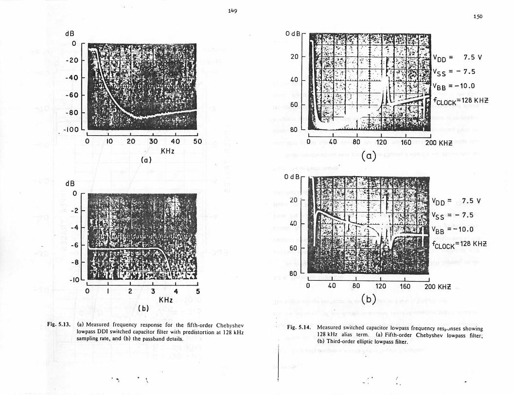
a
3
omoo
o
oCV
J
-O
1i
ii
i1
Oo
Oo
oo
LU
CV
J*
rto
CO
oT
3•
ii
1—
•
CD
•a
m
>i*
:in
IT)
oa
o
r-^
fv
oC
M
11
IIVll
IIII
o
ato
CD
<_)
fj
to
CD
o>
>>
«+-
rw
oo
-Q
-o
r%
8&
i£&
&a
*-i
*n
&M
'£&
MM
&S
-*
r
•*\x.f„*•'.'.*•'•
ir'^.'lt'
~•"
"*
x
ro
oa
CM
to
CO
u.
»
c>U
o(G
x:
8s
c11
«>
c1C
)
irS£
.4
J
re
0it0
JB
LU
ia*ou
re
U.
o
bUoi_
(/>o
JT3
re
3
3X
x:
rer^
W0
0.—
.
2™
*
>N
«X
•5•*
>,
oo
X5
<-J
-J
—x:
U«
u.C
-jo
T3
—
d-a
£-
Su
J3
Oo
K
uc-a
5.
J= 3£
JiQ
32
Q??
<"
c
COo
S
i/i00
Eh

OdB
-10
-20
-30-
-40-
a : 128 KHZ
b : 64 KHZ
151
-3dB
8 KHZ
Fig. 5.1S. Switched capacitor fifth-order Chebyshev lowpass frequencyresponse for different sampling rates.
152
5.2.3. Frequency Response versus Power Supply Variations
When the power supplies were changed from ±7.5 volts to ±5.0 volts, the
responses of Fig. 5.16 were obtained. The small changes in the response illustrates
the low sensitivity of the doubly-terminated switched capacitor ladder structure.
The supply voltage coefficient of absolute gain at 1 kHz is 0.03 dB/volt.
5.2.4. Harmonic Distortion
As discussed in Chapter 4, Total Harmonic Distortion (THD) depends on the
amplifier gain characteristics as well as the signal levels at the output of each
switched capacitor integrator in the filter. The signal levels are determined by the
transfer function from the input node to each of the integrator output nodes.
From Fig. 5.17, it is apparent that the signal levels are frequency dependent.
Hence, the THD is also frequency dependent as shown in Fig. 5.18. Chapter 4
described scaling techniques to reduce THD.
5.2.5. Noise Performance
Noise considerations were presented in Chapter 4 where it was shown that the
total filter output noise is equal to the entire noise output of the last stage plus
components from the other stages determined by the transfer functions from the
integrator outputs to the output of the filter. The noise at the output of an integra
tor consists of op amp noise, thermal noise of the MOSFET switches, and aliased
noise. Figure 5.19 displays the noise spectral density at the output of the Che
byshev filter.

3°-
309
552
«"O
»-i
&n
s=*
•
n*<
S3*
o^
%o
-'*
WT
3C
»
«<3
»<
=?
o=
r
ST6
Is.
2? 90*
—»
to
c*
3 Oo
o 3
3*
n a.
8fc
:•3
*•
O
(T)
o
O"1
»•
-T)
3*
3"
3o
•3 CC
Ln
<"*
O,
nO
S3
"0
0ff
in
o-
HH
<<
<7
0>
<^
<JJ
>C
Dto
oO
CD
too
oC
Oco
om
CD
co
om
II 1
ii 1
IIcr
••
IIII 1
IIQ •
•
^J
en
en
O•>
!•s
i
o»
OO <
o_
en
tn <
GA
IN
(dB
)
to
I0
00"
>Q
_J
CDo
-•—
J—
—-^
11
:
1 1
-^
1
ro
-
..
_L
.
!i::
!-;...
cr
"d"
.:..
-'
••"
t%
1m
i•-•
•'••
*.:
.;.:
.:.:
':J
--
\J4
"
T-r~
..„
i.
•r •I
'•;.
——
•
....
-^
-tJ_
..
.L
_.:
1
x>jL
.'.-..
!!
,g
7v
X
DD
IF
IFT
H-O
RD
ER
CH
EB
YS
HE
V
LO
WP
AS
SF
ILT
ER
-7
+•
10
00
20
00
30
00
HE
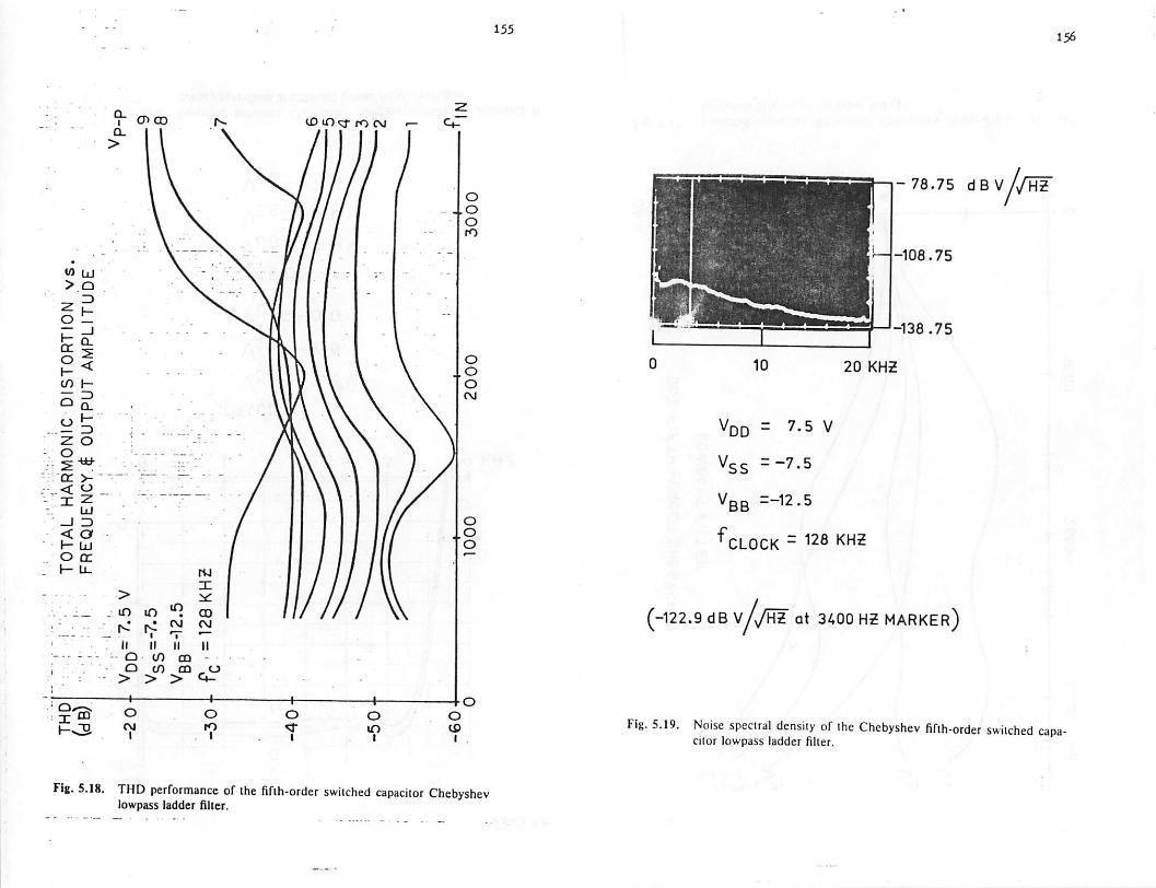
'o
H
*=X
•3a •3
f» •1 3)
3
o
n n
r1o n 5
TH
D
(dB)
-2
0-
-3
0-
-4
0-
*1
00 tn
MM _«c
n7
0o n
o
•a
Di
n
i/-
D,
f:.
Q.
ro
n Cfi
*<
nQ O 3"
< 3"
6 3.
VD
D=
7.5V
ro
fO » ID Q.
CD
< GO
O o X > 70
m to
TO
TA
LH
AR
MO
NIC
DIS
TO
RT
ION
vs.
FR
EQ
UE
NC
Y.$
OU
TP
UT
AM
PLIT
UD
E
10
00
-h
o r— o o
ro
03
7*
X
<C
DC
D II 1 ro
en
<
co II I~
o
en
<D D
II •o
ui
<
20
00 O
i—
o ro
o 7\
X
30
00
fc

157
5.3. LDI Switched Capacitor Third-Older Elliptic Lowpass Filter
In this section, the performance of the type-I LDI switched capacitor three-
pole, two-zero elliptic lowpass filter of Fig. 5.20 is described. The die photograph is
shown in Fig. 5.21. The three operational amplifiers with their associated switched
capacitors are shown in the right portion, white the integrating and zero-forming
capacitors are along the left portion of the photo. The zero-forming capacitors are
about 2 pF each, and are directly below the first and third integrating capacitors.
The integrating capacitors vary in size between 15 and 20 pF. The die size is
40 mils by 110 mils.
5.3.1. Frequency Response
The measured frequency response for a sampling rate of 128 kHz is given in
Fig. 5.22. Figure 5.22(a) shows the response over a wide range of frequencies.
The minimum stop-band rejection is about 30 dB with a transmission zero at about
9 kHz. The details of the passband are shown in Fig. 5.22(b). The measured ripple
bandwidth and total passband ripple are in excellent agreement with the design
goals of 3400 Hz, and 0.13 dB, respectively. A statistical distribution of insertion
loss, clipping level, and passband ripple are displayed in the histogram of Fig. 5.23
based on a sample size of 9 from a single processing run. Excellent process track
ing appears feasible with this approach.
Fig. 5.14(b) shows the alias term at 128 kHz.
Note that the insertion loss for this filter is 0 dB while the insertion loss of the
RLC doubly-terminated ladder prototype is 6 dB. In switched capacitor filters, the
insertion loss can be scaled by simply changing the size of the input switched capa
citor relative to the other switched capacitors. For example, the input capacitor,
shown at the bottom of Fig. 5.21, was doubled in the elliptic filter to increase the
158
Fiji. 5.20. Third-order elliptic lowpass type-1 LDI swiiched capacitor ladderfiller.

159
Fig. 5.21. Die photo of the third-order elliptic lowpass switched capacitorladder filler.
dB
0
-20
-40
-60
-80
-100 -
dB
0 r
-10 -
160
0)
Fig. 5.22. (a) Measured frequency response for the third-order ellipticswitched capacitor lowpass ladder filler clocked at 128 kHz, and(b) the passband details.

*
(A
o
O UI_l -J
oZ >-o o
1- >-cc 1-UI =>lO oz
— rti»» T
UI V_l
Q. COQ. CMM ^~
rr>-
o
X^-
ozUI
u. ao ui
cc
<a. xo uo oh- -Ien u
X
If)
o»o to ru
<o im 00CM
• -JOin
ocm Is
1-cc m
if) UI -otoz z
if)"~~i UI
_i
<r a.a.
CC 01lO _ TJ•"•
z z
cm < —
to
CO»— <
*a.
(0
s
k5
olO -jS5
UI
o> > 1-CM Ul <
CD K- XCM 3 id
a. _^r^ z<?
-1 1 P"" T^ — IO
in ff n n f- o
S1INH dO d3QWnN
161
Fig. 5.23. Histogram of passband ripple, insertion loss and THD for a sampleof 9 third-order elliptic switched capacitor lowpass ladder fillers.
' ^
162
gain by 6 dB, thus reducing the insertion loss to 0 dB.
5.3.2. Frequency Response versus Sampling Rate
Figure 5.24 shows the filter response for several values of clock frequency. In
Fig. 5.24(a), the response scales with low sampling rates until the leakage current is
significant during the long integration periods^ For this particular eaumple, the
minimum sampling rate is about 1 kHz. Fig. 5.24(b) shows the scaled responses
for several intermediate sampling frequencies, and Fig. 5.24(c) shows the response
at high sampling rates. At sampling frequencies above 300 kHz, the slewing and
settling errors in the amplifiers distort the frequency response. However, other
workers with higher performance amplifiers have observed that sampling frequen
cies approaching 1 MHz can be used before significant distortion occurs [45],[51].
Figure 5.25 illustrates the clipping level, noise, and passband ripple as a function of
clock frequency.
5.3.3. Frequency Response versus Power Supply Voltages
The measured frequency response for different power supplies is presented in
Fig. 5.26. The supply voltage coefficient of absolute gain at 1 kHz is 0.03 dB/volt.
5.3.4. Harmonic Distortion
The transfer functions from the filter input to each internal integrator output
are shown as functions of frequency in Fig. 5.27. The measured THD versus fre
quency is presented in Fig. 5.28, and THD versus signal level for a 1 kHz input is
shown in Fig. 5.29. For signal levels of about 0.3 volts RMS, THD is less than
0.1%. The increase in distortion at lower signal levels is due to the slight amount
of crossover distortion in the op amp transfer characteristics of Fig. 5.2.

OdB
- 20
- 40
-60
-80
163
Wm VDD= 7.5 V
P. VSS ="7.5VBB =-12.5
:iT*> -rz*3-, «*"« *-5»S ¥L:
^fSp^i; fC= 1,2,4 KHZ
0 200 400 600 800 1000 HE
(a)
7.5 V
Ifig fc=8J16,32,6AJ128KHZ
7.5 V
-Fr=128,200,256,300 KHZ
20 30 AO 50 KHZ
(c)Fig. 5.24. Swiiched capacitor third-order elliptic lowpass frequency response
versus sampling rale.
wu "ivnois indino QH1 y.iaod SV,°A ni TVN9IS lfldN 1 *xvw
o CO tP <r CM O
(O CM CM CM CM CM
XOOIO^, O100T0 ZH>I 921IV ZH *.*'£)S3WI1 9Q920* IV Q P 3"lddlet
8 CO lX> <T CM o
• • • *
OI00T0 ZHM8211V2HX2)XOOlOj. l?9/l IV ZH//A9P NI 3SI0N
— rO in r- o» lOo o o o O r—
i \
1•
/ 1 o
• CM
.«•«.CM
CO o> * IU
<o • o x_J UI< -J £/
§*z o Q. • z
2 S 5/CO >-
>- •*7 UI o
•s 1- t/ -J o z
IAXIMUICY(DU
I•
\
o.Q.
CC
UICO
oz|
^" UI•"" 3
orUICCu.
^ z * o-«*• UI \ o *
« 3 • • — o
uJ Of \ o_l ui -J
Q. CC\
u
o. U.
cc *~ o
\• it j
o.(9
UI O t /to _J
5 ° 1 l>z
v
o.CM
164
Fig. 5.25. Measured noise spectral density, passband ripple and clipping levelversus clock rate for the elliptic third-order switched capacitorlowpass ladder filter.
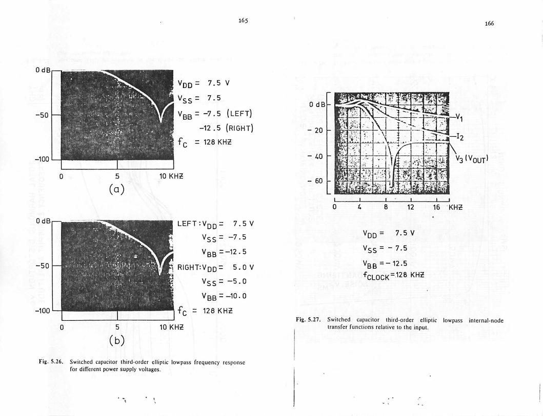
OdB
-50
-100
OdB
-50
-100
165
DD = 7.5 V
VSS= 7.5
BB= -7.5 (LEFT)
-12.5 (RIGHT)
fc = 128 KHZ
10 KHZ
LEFT:VDDr 7.5V
VSS= -7.5
VBB=-12.5
RIGHT:VDD= 5.0 V
vSs- -5-0
VBB = -10.0
fc = 128 KHZ
10 KHZ
Fig. 5.26. Swiiched capacitor third-order elliptic lowpass frequency responsefor different power supply voltages.
166
OdB-
- 20 -
- 40 V3lVoUT>
- 60
16 KHZ
VDD= 7.5 V
ss = - 7.5
VBB=-12.5
fCL0CK =12B KHZ
Fig. 5.27. Swiiched capacitor third-order elliptic lowpass internal-nodetransfer functions relative to the input.

82
•OC
B
«">
«/>
5/
C
Hn
_Q
.
3H
gD
</> *»
2
=»
2
05*"
3_
^cb
a.' ?i. C
B
O.
6 Q.
•o~
2.°
:^
3*
£=
;•c
9-S
go
-n
s.
a.
65n
3£
?»
elf
2.r.
res
<•><
I£
V)
...
«-»
«»
^»
i3
_»
"H
.
cbcb
e
SO
r.
SE
S
3N
CB
5'
«*>
—2
.=>
•£
U)
CB
nro
Q.
HD
[dB) I -
30
-V
DD
=7.
5VV
ss=
-7.5
VB
B^2
.5
TO
TA
LH
AR
MO
NIC
DIS
TO
RT
ION
vs
FR
EQ
UE
NC
Y£
OU
TP
UT
AM
PL
ITU
DE
-40
•fc
=12
8KH
2
-6
0•
Vp
»,.
ON
&

169
5.3.5. Noise Performance
The output noise spectral density versus frequency is pictured in Fig. 5.30 for
a spectrum analyzer bandwidth of 100 Hz. The sampling rate was 128 kHz.
5.3.6. Power Supply Rejection
The measured supply rejection is presented in Fig. 5.31 for all power supplies
and clocks. The rejection can be increased by more careful layout which includes
shielding wherever required. Higher performance amplifiers would also improve
this specification.
5.3.7. Phase Sensitivity
The phase at the 3400 Hz cutoff frequency was measured for different samples
with variations in dock frequency, clock duty cycle, and temperature. The results
given in Table II show that the switched capacitor doubly-terminated ladder filters
have very low phase sensitivity in addition to low magnitude sensitivity.
5.3.8. Temperature Performance
Three samples were tested at 0, 25, and 65 degrees C. Noise remained con
stant over temperature; the insertion loss at 1000 Hz changed less than 0.1 dB, and
the passband ripple-changed less than 0.05 dB for a 2.8 VRMS input signal. The
temperature coefficient of absolute gain at 1 kHz was about 0.0006 dB/°C.
5.3.9. Intermodulation Distortion
The measured intermodulation distortion versus applied signal level is
displayed in Fig. 5.32.
80 r
>
4.
- 40
CD
o
0 L
n 0
co
uo
40 -
-1.80
10 kHz
a>
170
Fig. 5.30. Output noise for the third-order elliptic lowpass switched capacitorladder filter. Analyzer bandwidth is 100 Hz.

171
OdBi
-20
-40
-60
OdB
-20
-40
-60
VBB SUPPLY REJECTION
10
(°)
VDD=7.5V
VSS =-7.5VBB=-12.5
+
20KHZ
Vss SUPPLY REJECTION
10
(b)
+
20KHZ
Fig. 5.31. Measured power supply rejection for the third-order elliptic lowpassswitched capacitor ladder filter, (a) VBB supply; (b) Vss supply.
OdBx
-20..
-40
-60
OdB
-20..
-40..
-60
0
172
VDD SUPPLY REJECTION
10
(0
10
(d)
VDD =7.5V
VBB=-12.5
20KHZ
0} REJECTION
0o REJECTION
+
20KHZ
Fig. 5.31. Measured power supply rejection for the third-order elliptic lowpassswitched capacitor ladder filter, (c) VDD supply; (d) clocks.
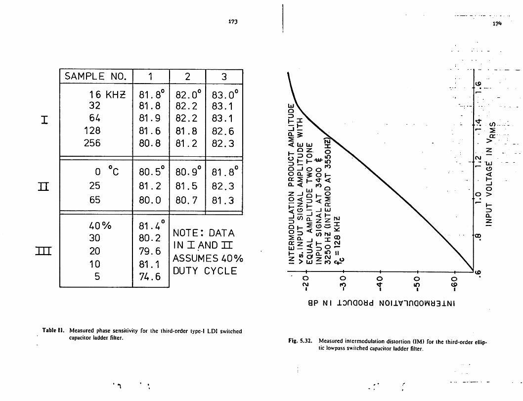
n
m
173
SAMPLE NO. 1 2 3
16 KHZ32
64
128
256
81.8°81.8
81.9
81.6
80.8
82.0°82.2
82.2
81.8
81.2
83.0°83.1
83.1
82.6
82.3
0 °C25
65
80.5°81.2
80.0
80.9°81.5
80.7
81.8°82.3
81.3
40%
30
20
10
5
81.4°80.2
79.6
81.1
74.6
note: DATA
IN I AND XT
ASSUMES 40%
DUTY CYCLE
Table II. Measured phase sensitivity for the third-order type-1 LDI swiichedcapacitor ladder filler.
' 1
ts
17**
CO
cc>
CM
- 1x1O<
_J
OO >
3cl-
Ul\•.
o \3 X -
hl\^~ \Gt ^ X.s W< LU LU ?. Q z o[TDO uo
_.
g^Oha: 2 H «- <-
LU S .
Z-l5l-2
H 2 ^ F,!< o —; _J lli
l*izz ru
? °- _l x GO
£?<S°CM
± > uj £ ro
1
II
1 1 1 1
co
o O o o oCM CO <fr m (9
i 1 1 1
qp ni lonoodd NOiivnnaorNd3iNi
<x>
Fig. 5.32. Measured intermodulation distortion (IM) for the third-order elliptic lowpass switched capacitor ladder filter.

175
5.3.10. Quantizing Noise
The output of switched capacitor filters changes in small steps at each integra
tion time as shown in Fig. 5.33. Hence, there are components at the clock fre
quency due both to clock feedthrough and to signal transitions. In this context,
quantizing noise is defined as the total magnitude of the signal at the sampling fre
quency in a 1 Hz bandwidth, and isdisplayed in Fig. 5.29. When the input signal is
very small, the quantizing noise is due almost entirely to clock feedthrough which
for the metal-gate process used in these experiments is about 75 mV.
176
VERT. 500mV/DIV
HOR. 200JUS/DIV
VDD= 7.5 V
vSs=-7-5VBB=-12.5
= 128 KHZCLOCK
f,N=lKH2
VERT. 500 mV/DIV
H0R.200JJS/DIV
VDD= 7.5 V
Vss=-7.5
VBB=-12.5
"FcLOCKf|N=3KH2
= 128KHZ
Fig. 5.33. Output waveforms for the third-order elliptic lowpass swiichedcapacitor ladder filler clocked ai 128 kHz.

177
Chapter 6
AN ELECTRICALLY-PROGRAMMABLE SWITCHED CAPACITOR FILTER
Switched capacitor techniques have been used to integrate frequency selective
filters using standard MOS technology Ill],I13]-I15J,l24j-l25]. In determining the
usefulness of this approach for a given application, the obvious advantages of
integration such as small size and low manufacturing cost must be weighed against
the disadvantages of the cost and time required to mask program a desired filter
response. This restricts the usefulness of these fillers to those applications with
sufficient manufacturing volume to justify the expense of mask programming, and
it completely eliminates their use in applications that require a time-varying
response such as adaptive filters and speech and music synthesizers. A monolithic
filter which can be programmed by the application of digital control signals would
therefore find widespread use, and is the subject of this chapter [59].
6.1. Synthesis of the Programmable Second-Order Section
In this section, the synthesis approach will be described using s-plane notation.
The singly-terminated RLC second-order lowpass filler shown in Fig. 6.1(a) was
chosen as the prototype for this design because it can be configured in an active
form in which the peak gain (G), selectivity (Q), and center frequency (o*0) are
independently programmable. To illustrate this very important point, compare the
general form of the transfer function for a second-order lowpass filler which is
given by
H(s)
s2+s^+t-0(6.1)
where k is a constant, to the transfer function for the RLC circuit of Fig. 6.1(a)
178
R
(o)
1/0 i/<j,
Vinf t^l/Wo fvoutv2
I2t
(b)
Fig. 6.1. (a) The singly-terminated RLC second-order lowpass prototype and(b) an equivalent form after impedance scaling; (c) the corresponding signal flowgraph.

which is given by
1
LCH(s)
^b-k
179
(6.2)
In order to obtain programmability, Eqns. (6.1) and (6.2) are equated to solve for L
and C in terms of w0 and Q to obtain:
-M (6.3a)
and
RQo»0'(6.3b)
For given values of R and w0, it is apparent that the values for L and C become
widely separated (proportional to Q2) asQ becomes large which is undesirable since
it would result in a similar spread in the required capacitor ratios in a switched capa
citor implementation. Fortunately, a significant improvement is obtained if the
impedances are scaled so that the termination resistance, R, is equal to — since the
L and C values then become
(6.4a)«o wo
and
C-1 _ 1 (6.4b)
*kK -
180
After scaling, Ihe reactive elemeni values are equal and are determined by the
center frequency independently of Q and peak gain. The scaled RLC prototype is
shown in Fig. 6.1(b), and acorresponding signal flowgraph is shown in Fig. 6.1(c).
The switched capacitor circuit which implements the flowgraph of Fig. 6.1(c)
would usually be realized with only the two operational amplifiers required to
implement the two integrators. In this case, however, the termination path
presents a practical problem because for high Q, the swiiched capacitor which
implements the -^ termination becomes very small (0.01 pF). Therefore, it was
decided to use a third operational amplifier to realize the — terminationaround the
bandpass stage, and to set the peak gain through the filter. The third operational
amplifier is used in a charge multiplier configuration as shown in Fig. 6.2 with a
minimum capacitor size of Cs«=0.42 pF. In order to insure DCstability against leak
age currents and power-up transients, a switched capacitor resistor was connected
across CQ. It is interesting to note that the filter ofFig. 6.2 has the same form as a
second-order state-variable filler 160]. It thus retains many of the advantageous
state-variable properties including low sensitiviiiy to component variations, and the
availably of lowpass, bandpass, and bandreject outputs.
6.2. Design of the Programmable Switched Capacitor Arrays
There are several considerations in determining what type of capacitor arrays
to use for programming the switched capacitor filler response. The silicon area
required for the arrays should of course be minimized while maintaining a large
enough unit capacitor size to provide good matching accuracy. More importantly,
the arrays must be designed so that capacitor switching during dynamic program
ming will not distort the response or create largedisplacement currents. With these
considerations in mind, two different types of capacitor arrays were designed for
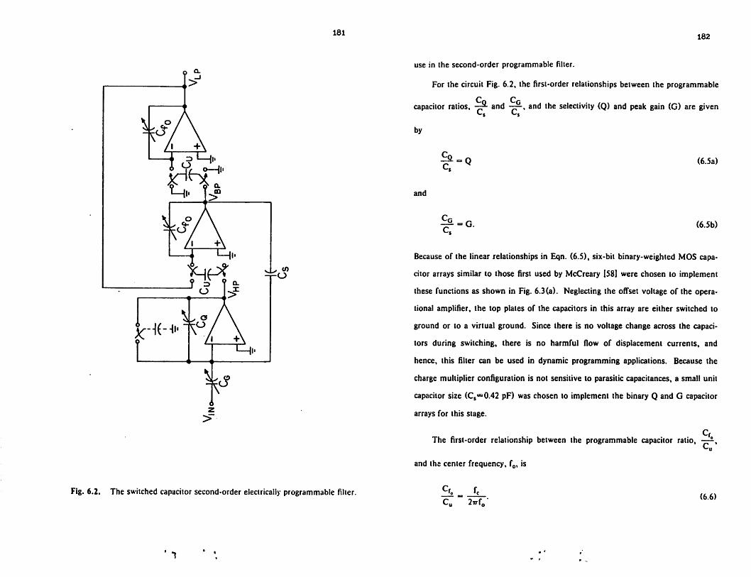
181
Fig. 6.2. The switched capacitor second-order electrically programmable filler.
' 1
182
use in the second-order programmable filter.
For the circuit Fig. 6.2, the first-order relationships between the programmable
capacitor ratios, -rp- and -rp-t and the selectivity (Q) and peak gain (G) are given
by
Co_(6.5a)
and
Cs(6.5b)
Because of the linear relationships in Eqn. (6.5), six-bit binary-weighted MOS capa
citor arrays similar to those first used by McCreary [58] were chosen to implement
these functions as shown in Fig. 6.3(a). Neglecting the offset voltage of the opera
tional amplifier, the top plates of the capacitors in this array are either switched to
ground or to a virtual ground. Since there is no voltage change across the capaci
tors during switching, there is no harmful flow of displacement currents, and
hence, this filter can be used in dynamic programming applications. Because the
charge multiplier configuration is not sensitive to parasitic capacitances, a small unit
capacitor size (Cs=0.42 pF) was chosen to implement the binary Q and G capacitor
arrays for this stage.
The first-order relationship between the programmable capacitor ratio, —-,
and the center frequency, f0, is
cu 27Tf„(6.6)

-31-
so z
s3 1
lc-)l-•o e
^h'0 91
Ac—51—soze
u
J—li
ftHn3 9Z.Z.9*0
•ft—HLn0 9Z.99TJ
ftn3 18870
[Jn0 99*770
-ftfjn0£8ir0
-ft[|n3 29ZE*0
-ftn0 8998"0
183
ii .o
n0 9C98£ L t
<> I—|i
Fig. 6.3. (a) The six-bit binary-weighted capacitor array used to program thegain and the selectivity, and (b) the non-binary capacitor array usedto program the center frequency.
184
It was desired to have the center frequencies logarithmically span an octave of fre
quency such that when the sampling rate was changed by a factor of two, a new set
of center frequencies would be obtained which would smoothly continue the loga
rithmic progression. Since the relationship in Eqn. (6.6) is an inverse (and because
of the logarithmic progression), binary-weighted capacitor arrays were not suitable
for center frequency programming. Therefore, a more flexible type of MOS capaci
tor array was developed as shown in Fig. 6.3(b). The amount of capacitance
selected in this array is determined by turning on all the MOS switches except one.
The switch which is off electrically separates the array into two parts. The value of
capacitance determining f0 is the sum of all capacitors between the off switch and
the op amp. As in the binary arrays, the remaining capacitors to the right of the off
switch are connected to ground so that the displacement current generated during
program switching is minimized.
In Fig. 6.4, the capacitance ratios required to program eight different center
frequencies with 1.089 logarithmic spacings are given for a clock rate of 10 kHz.
The values of the capacitors which are programmed in the non-binary array are
determined by the difference between adjacent capacitor ratios as shown in the
graph. This type of array is extremely efficient in its use of capacitor area. For
example, in order to obtain the lowest center frequency of 225 Hz, a capacitor ratio
of 7.07 is required, and since the total capacitance in the array is 7.07 unit squares,
no silicon area is wasted. Type-I LDI integrators were used to implement the filter,
and Cu was chosen to be about 2.6 pF. In this particular design, there is no
significant performance advantage in using type-11 LDI integrators since Cu must be
several picofarads in order to accurately realize the fractional unit capacitors
required in the Cfo arrays. It will be shown later that the error introduced by the
top-plate parasitic capacitance is very small.

185
Fig. 6.4. Capacitor ratio versus center frequency. The non-binary capacitorvalues are determined by the difference between successive capacitor ratios.
186
Eqn. (6.6) also shows a direct one-to-one relationship between f0 and fc.
Therefore, for a given capacitor ratio, the sampling frequency can be used to pro
gram the center frequencies of the filler. This programming technique was also
used in the formant speech synthesis filter to be described later in this chapter. In
the next section, the practical design considerations for the switched capacitor pro
grammable second-order section will be presented.
6.3. Practical Design Considerations
The practical limitations of the MOS operational amplifiers, parasitic capaci
tances, and other nonidealities can affect the performance of switched capacitor
fillers. In some cases where the filter specifications are relatively relaxed as in a
formant speech synthesizer, frequency response deviations can be tolerated if they
are predictable. In cases where the specifications are tighter, it may be necessary to
compensate or predistort to eliminate these errors. Therefore, it is important for
both cases to develop a set of design equations which relate the actual filter perfor
mance to the parameters of the individual components. In this section, the practi
cal design considerations for the programmable second-order filter will be
presented.
6.3.1. Sampled-Data Transfer Functions
The switched capacitor implementation has a frequency response which is
slightly different from the response of the RLC prototype due to the termination
errors introduced by the finite switching frequency. The sampled-data transfer
functions are given below:
-fe]l2(22+a'2+1)l"br<z> - [ V. ,.. r—b3z3+b2z2+b,z+b0 (6.7a)
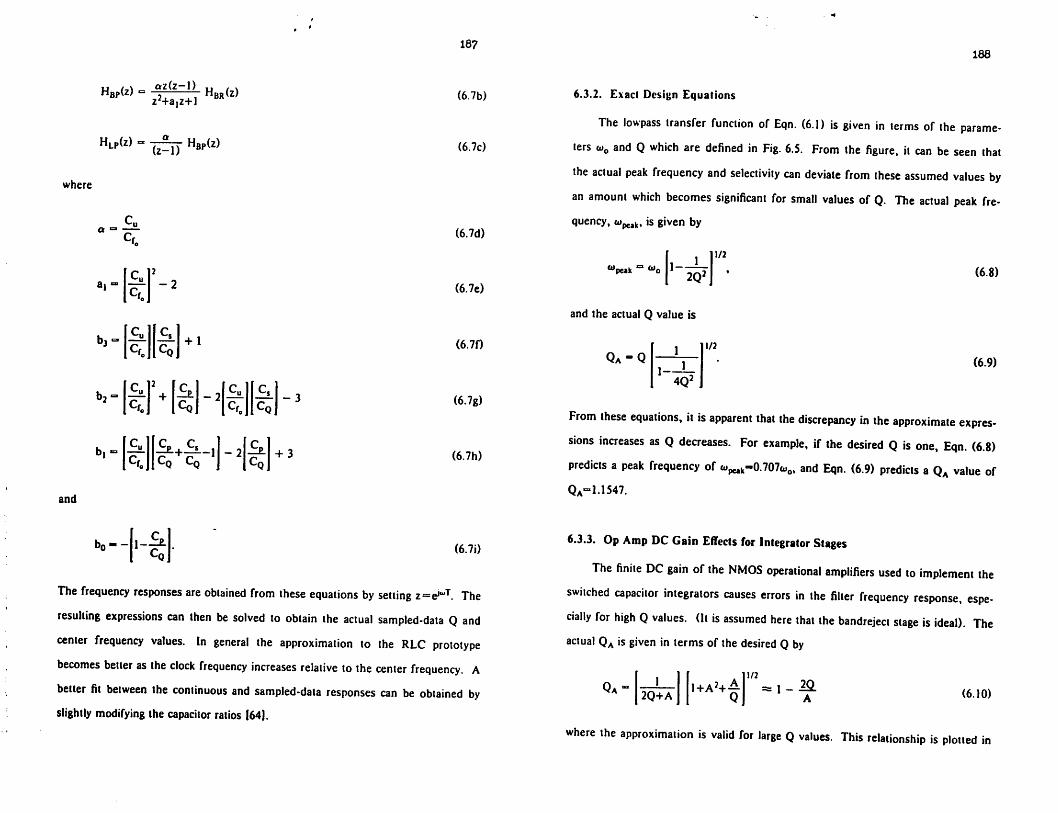
"-"-s^"-"
HLP(z)(z-1)
HBP(z)
where
and
«i[cuj 2
-2
[CullCreJ
[c$C0
+ 1
fc 1'-u2
+ cQj -2[cu] [cs
ICQ
[cu|Co
—1>
-2
cqJ
bn--!-^-
-3
+ 3
187
(6.7b)
(6.7c)
(6.7d)
(6.7e)
(6.7f)
(6.7g)
(6.7h)
(6.7i)
The frequency responses are obtained from these equations by setting z=e"uT. The
resulting expressions can then be solved to obtain the actual sampled-data Q and
center frequency values. In general the approximation to the RLC prototype
becomes better as the clock frequency increases relative to the center frequency. A
better fit between the continuous and sampled-data responses can be obtained by
slightly modifying the capacitor ratios (64].
188
6.3.2. Exact Design Equations
The lowpass transfer function of Eqn. (6.1) is given in terms of the parame
ters o>0 and Q which are defined in Fig. 6.5. From the figure, it can be seen that
the actual peak frequency and selectivity can deviate from these assumed values by
an amount which becomes significant for small values of Q. The actual peak fre
quency, Wpeak, is given by
"peak 1 —2Q3
1/2
(6.8)
and the actual Q value is
Qa = Q1-
4Q2
1/2
(6.9)
From these equations, it is apparent that the discrepancy in the approximate expres
sions increases as Q decreases. For example, if the desired Qis one, Eqn. (6.8)
predicts apeak frequency ofa.pe,k-0.707a,o, and Eqn. (6.9) predicts aQA value ofQA=1.1547.
6.3.3. Op Amp DC Gain Effects for Integrator Stages
The finite DC gain of the NMOS operational amplifiers used to implement the
switched capacitor integrators causes errors in the filler frequency response, espe
cially for high Qvalues. (It is assumed here that the bandreject stage is ideal). Theactual QA is given in terms of the desired Q by
2Q+Al+A2+4
1/2
=,i_ia(6.10)
where the approximation is valid for large Qvalues. This relationship is plottedin
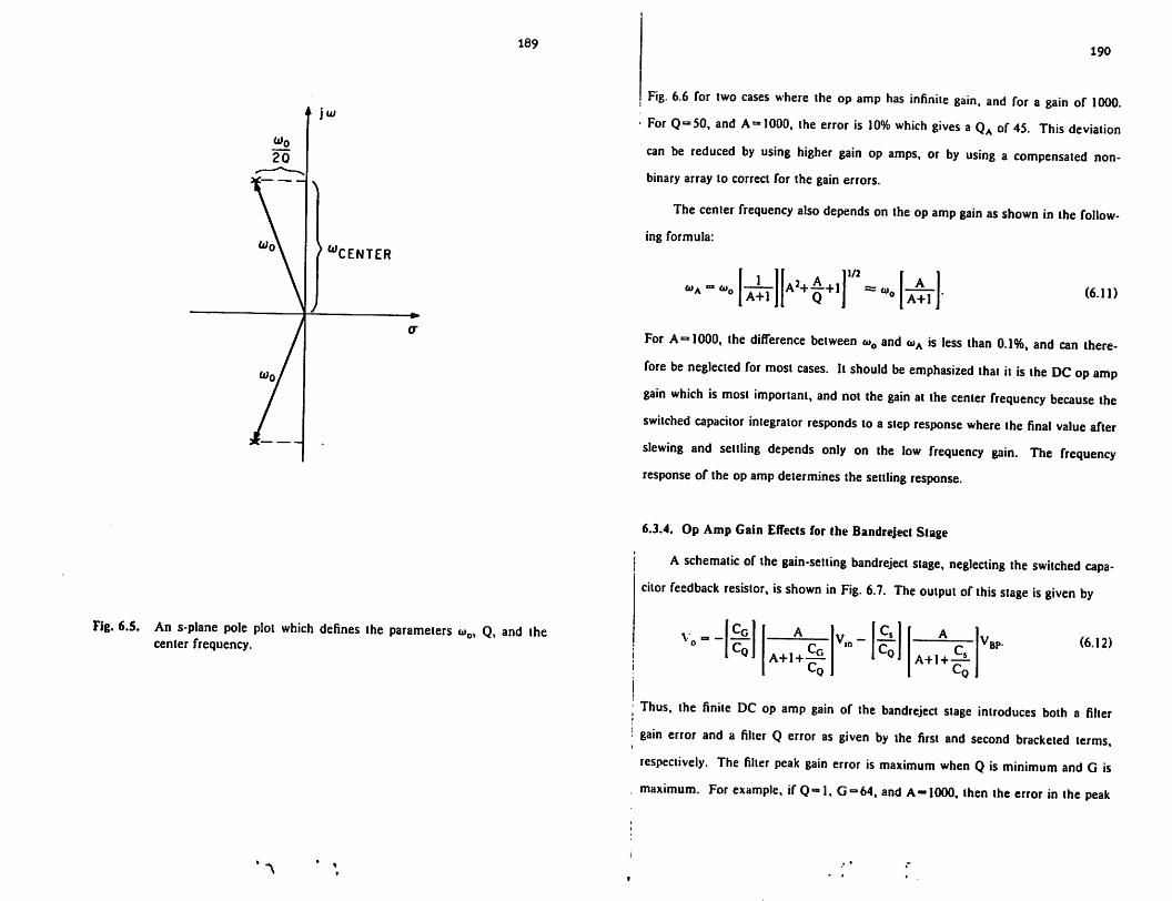
189
CENTER
Fig. 6.5. An s-plane pole plot which defines the parameters o»0, Q, and thecenter frequency.
190
Fig. 6.6 for two cases where the op amp has infinite gain, and for a gain of 1000.
For Q=50, and A-1000, the error is 10% which gives aQA of 45. This deviation
can be reduced by using higher gain op amps, or by using a compensated non-
binary array to correct for the gain errors.
The center frequency also depends on the op amp gain as shown in the follow
ing formula:
1
A+l
a \mA2+A+,J ^A+l
(6.11)
For A=1000, the difference between o>0 and oiA is less than 0.1%, and can there
fore be neglected for most cases. It should be emphasized that it is the DC op amp
gain which is most important, and not the gain at the center frequency because the
switched capacitor integrator responds to astep response where the final value after
slewing and settling depends only on the low frequency gain. The frequency
response of the op ampdetermines the settling response.
6.3.4. Op Amp Gain Effects for the Bandreject Stage
A schematic of the gain-setting bandreject stage, neglecting the switched capa
citor feedback resistor, is shown in Fig. 6.7. The output ofthis stage is given by
A+l+-^-V.„-
Cs
^0A+1+-
'BP- (6.12)
Thus, the finite DC op amp gain of the bandreject stage introduces both a filter
gain error and a filter Q error as given by the first and second bracketed terms,
respectively. The filler peak gain error is maximum when Q is minimum and G is
maximum. For example, if Q-l, G=64, and A-1000, then the error in the peak

191
Q
Fig. 6.6. A graph of Q versus desired Q for two different values of DC opamp gain for the two amplifiers used to implement the switchedcapacitor integrators.
192
IN o- -tf-
V_ o.BP ^f
OUT
Fig. 6.7. A simplified schematic of the gain-selling bandreject siage.

193
gain is about 6%. The Q error is worst-case for minimum Q and G. If G = l,
Q=l, and A = 1000, the Q error is only about 0.2%.
6.3.5. Top-Plate Parasitic Capacitance
Since type-I LDI integrators were used in this design, it is important to con
sider the effect of the parasitic capacitance connected to the top-plate of the
switched capacitors. For a switched capacitor value of Cu, and a top-plate parasitic
capacitance of Cp, the center frequency (assuming everything else is ideal) is
n 11/2
Qa = Q
and the actual Q value is given by
t/2
•4
(6.13)
(6.14)
In this design, the switched capacitor size was about 2.3 pF, and the top-plate
parasitic was about 0.025 pF. Thus, the error due to top-plate parasitic is only
about 0.5% which is negligible for the formant speech synthesizer application. If
necessary, type-11 integrators could be used to obtain greater accuracy.
6.4. NMOS Prototype Experimental Results
An experimental prototype of the electrically programmable second-order
switched capacitor filter shown schematically in Fig. 6.2 has been integrated using
the NMOS metal-gate enhancement-depletion process described in Appendix 1. A
photograph of the 88 mils by 105 mils (including bonding pads) die is shown in
Fig. 6.8. The NMOS operational amplifier used in this circuit is identical to the one
described in Chapter 5. The programmable filter can produce 32,768 (2,s) different
•<•>
(a)
f0 ARRAY DIGITAL
LP
STAGE
Q
ARRAY ,
LOGIC
G
ARRAYBP
STAGE
BR
STAGE
f0 ARRAY
19**
(b)Fig. 6.8. (a) A die photograph of the 88 mils by 105 mils NMOS experimen
tal chip, and (b) a layout block diagram of (a).

195
frequency responses at each of the lowpass, bandpass, and bandreject outputs for
each clock frequency. Representative experimental results are presented in the fol
lowing sections.
6.4.1. Center Frequency Programming
By applying a 3-bit digital word to the two non-binary arrays, any one of eight
different center frequencies can be programmed. As mentioned earlier, the center
frequencies were designed with logarithmic spacings where f0(n) = 1.089fo(n—1).
The eight experimentally observed center frequencies shown in Fig. 6.9 for a
20 kHz clock rate are in good agreement with the expected design values.
6.4.2. Clock Frequency Programming
The gain constant of a switched capacitor integrator, o>0=fc , is directly
proportional to the sampling frequency. This one-to-one relationship can also be
used as a degree of freedom in programming a switched capacitor filter. Since fre
quency division by a factor of two is easily achieved using standard flip-flops, this
filter was designed in such a way thai when the clock rate was changed by a factor
of two, a new set of center frequencies was generated which smoothly continued
the logarithmic progression as illustrated in Fig. 6.10. Thus, with a 1 kHz
minimum clock frequency and a 256 kHz maximum clock rale, the center frequen
cies range over eight octaves from 22.5 Hz to 10573 Hz in 1.089 logarithmic steps.
dB
On
-40-
-80-
0 500
196
000 Hz
Fig. 6.9. The eight experimentally observed programmable center frequenciesfor a 20 kHz clock rate.

dB
0-.
-40-
-80-
^££^y^£#i^&;;t^&;--
dB
On
-40-
-80J
800
500
1300
—l
000
Hz
800
Hz
197
Fig. 6.10. The eight experimentally observed center frequencies for 20 kHzand 40 kHz clocks. The filter is designed so that the logarithmicprogression of center frequencies is smoothly continued as thesampling rate is changed by a factor of two.
198
6.4.3. Selectivity Programming
A six-bit digital word is used to program a binary-weighted capacitor array to
any one of 64 different Q values from Q=l to Q=64. Figure 6.11 shows five of
the possible 64 values ranging from four to 64 by factors of two. Notice that the
highest experimental Q is about 56. The deviation from the desired value of 64 is
due to finite DC op amp gain of 1000 as described earlier.
6.4.4. Gain Programming
A six-bit binary word is also used to program the peak gain through the filter.
Figure 6.12 shows seven of the possible 64 G values ranging from one to 64 by fac
tors of two. Good agreement is observed between theory and experiment.
6.4.5. Low-Q Passband Details
For low-Q applications, there is a significant difference between the actual
values for the center frequency and gain and the parameters w0 and Q due to the
theoretical approximations used in Section 6.3. The experimental passband details
of Figure 6.13 show that as Q is decreased, and these approximations become
invalid, the peak frequency is reduced such that when Q is one, 01^-0.707010, and
the gain is increased by about 1.25dB. For Q ^5, these discrepancies are less than
1%.
6.4.6. Dynamic Range
The output dynamic range was measured for maximum and minimum values
of Q and peak gain. The noisecontributed at the output of the filler by the internal
op amps and their associated switched capacitor resistors is amplified by an amount
equal to Q, and hence, the dynamic range decreases for higher Q's. The distortion

dB
On
-50-
-100
199
^TOjriBGF5!^rarsp^»
o 500 1000
6.11. Experimental results for five of the possible 64 programmable Qvalues.
dB
40
20-
0-
20
-40
0
200
5 00 000 Hz
Fig. 6.12. Experimental results for seven of the possible 64 programmablepeak gain values.

dB
2-i
0-
-2-
-4-
-6-
0 500
201
000 HZ
Fig. 6.13. Low Q passband details for a 20 kHz clock rate.
202
at the ouiput remains relatively constant. Preliminary results indicate a dynamic
range of from 65-90 dB as Q is varied from one to 64 for fo-»450 Hz at a 20 kHz
clock rate. Complete dynamic range data will be published at a later dale |61].
6.5. A Formant Speech Synthesis System
There are many applications which require electrically programmable filters
including adaptive equalizers, and music and speech synthesizers. This section will
describe an application wherein several swiiched capacitor second-order sections are
dynamically programmed to implement a formant speech synthesis system. The
major advantage of the formant algorithm is that good quality speech can be syn
thesized with a low data rate of about 300 bits/second [62].
6.5.1. The Vocal Tract Model
Figure 6.14(a) shows a cross-section of the male vocal tract which is a lossy
acoustic tube about 17 cm in length. Theoretically, this lube has an infinite number
of natural frequencies or formams. In order to produce different sounds, the fre
quency response characteristics of the vocal tract are altered by changing the cross-
sectional area of the tube at the tongue, lips or teeth.
There are several methods by which the vocal tract responses can be electri
cally simulated 162]. One method of electrically modelling the vocal tract is shown
in Fig. 6.14(b). In this model, a distributed LC ladder is used in which each LC
pair contributes to a resonant frequency. The main disadvantage of this approach is
that it is very difficult to independently program the formanls. Therefore, it was
decided to use a cascade of electrically-programmable swiiched capacitor second-
order sections which allows the gain, Q, and formant frequencies to be indepen
dently controlled.

203
Fig. 6.14. (a) A cross-section of the male vocal tract, and (b) a distributedLC ladder electrical model.
204
6.5.2. A Swiiched Capacitor Formant Synthesizer
A block diagram of the formant synthesis system is shown in Figure 6.15. It
has been shown experimentally that good quality speech can be obtained by simu
lating only the three low frequency formants 162]. These three formants are imple
mented with second-order switched capacitor filters which have their gain, center
frequency and selectivity programmed by a digital controller. In addition, it has
been shown that all of the higher frequency formants can be empirically modelled
using high-order pole correction with a fixed response. In this case, two poles with
center frequencies above the third formant are used as correction. The response of
this filter is dynamically programmed every 1-10 msec to produce the synthesized
speech.
As mentioned earlier, the clock frequency can be changed to program these
filters, and this feature has been exploited in the formant synthesizer. The first
formant stage is clocked at 10/20 kHz, the second at 30/60 kHz, and third at
60/120 kHz. Since there are 32768 responses/output/clock frequency, and since
there are five different clock frequencies, there are 3.78 x 10²² possible different
responses for this system!
At the present time, the English vowels have been synthesized with excellent
results. Figure 6.16 shows two different vocal tract responses for the vowels /a/ as
in "father", and Id as in "bet", and their corresponding time wavef"rms. This sys
tem is currently being characterized and the complete results will be published at a
later date [63].

•n
no3
),
3 3,
nO
"
roo o *
r
3 a
30
00
*ro
3 o
ron
inc?
rr
3£-
••
•0
9<
3r;
"*
*•a
ro o.
»*
_J
n
—*
ror:
n
•a
•<
orr
ft3"
f2
Q.
to
2.
*
-a
c
oo
?B R
3^
CL
OC
KG
EN
ER
AT
OR
VO
ICE
DV
VV
VV
FIR
ST
FO
RM
AN
T—
>
SE
CO
ND
FO
RM
AN
T—
>
TH
IRD
FO
RM
AN
T—
>
FO
UR
TH
FO
RM
AN
T
(FIX
ED
)
—>
FIF
TH
FO
RM
AN
T
(FIX
ED)
a T
UN
VO
ICE
D
INP
UT
Oi
3i
e2
f4)
e3
n.
A
G5
PA
RA
ME
TE
RIN
TE
RP
OL
AT
ION
/v.
/s
PA
RA
ME
TE
RS
TO
RA
GE
Q \
^^f^g
^P
^^I^
8
ro
207
Chapter 7
CONCLUSIONS
A new approach for designing precision high-order switched capacitor filters
has been developed which uses state-variable techniques to simulate passive RLC
ladder networks. Switched capacitor ladder filters have several important advan
tages over other approaches: (1) The low sensitivity of the passband response of
the RLC ladder prototype to component variations is retained in the switched capa
citor active ladder equivalent network; (2) by simulating conventional RLC filters,
there are many design tables available which can be used to obtain prototypes for
synthesizing switched capacitor filters, and (3) since the switched capacitor response
depends on monolithic MOS capacitor ratios and clock frequency as the precision
components, very precise responses can be obtained which are insensitive to tem
perature and processing variations.
The relationship between the phase shift of the sampled-data integrator and
the frequency response of the switched capacitor ladder filter has been investigated,
and three techniques have been developed for clocking switched capacitor filters.
The type-II LDI clocking is the simplest and has the additional advantage that the
dependence of the frequency response on all parasitic capacitances is eliminated.
The fundamental limitations on dynamic range have been explored, and
several new techniques have been presented for scaling switched capacitor filters.
The noise performance of the switched capacitor integrator has been analyzed in
terms of the op amp noise, and the switched capacitor resistor noise.
Three experimental NMOS prototypes have been designed and fabricated.
These filters demonstrated wide dynamic range, low power dissipation and
208
insensitivity to component variations. One circuit verified a new technique for
designing switched capacitor filters using switched weighted capacitor arrays to
achieve digitally-programmable frequency responses.
There are several areas where future work may be directed: (1) Reducing the
required number of operational amplifiers; (2) high frequency switched capacitor
filters; (3) maximum dynamic range filters; (4) N-path filters; (5) minimum area
realizations, and (6) the development of bilinear switched capacitor integrators
which are insensitive to parasitic capacitances.

Appendix 1
NMOS METAL-GATE ENHANCEMENT-DEPLETION PROCESS
209
This appendix details the NMOS process used to fabricate the switched capaci
tor filters described in this dissertation. The process evolved to its present form
through previous efforts [53],(58). Boron diffusions are used as isolation regions,
and the substrate is boron-doped p-type <100> orientation with 25-50 ohm-cm
resistivity.
Fabrication Sequence
1. Initial wafer cleaning:
(a). Deionized water DI:HF (9:1), room temperature dip for 2 mins.
(b). TCE, 60 ° C for 10 mins.
(c). Acetone, room temperature for 2 mins.
(d). DI rinse.
(e). Clean for 15 mins. in H2S04:H202 (4:1) at 90 ° C (piranha cleaning
step).
(0. DI rinse.
(g). N2 blow dry.
2. Inital oxidation: N-type drive-in furnace, 0.92 jun of oxide,
(a). Wet 02 at 0.5 liters/min, 1150 ° C, 90 mins.
(b). Dry N2 at 0.65 liters/min, 850 ° C, 10 mins.
3. Negative photoresist step: (p+ isolation diffusion mask)
(a). Apply Kodak 747 Micronegative Photoresist; spin at 5000 rpm for
30 sees.
210
(b). Air dry for 15 mins.
(c). Prebake at 90 ° C for 30 mins.
(d). Expose mask, 3.5 sees.
(e). Spray develop, 30 sees.
(0. Spray rinse, 20 sees.
(g). Alcohol dip, 7 sees. Isopzopylrmethanol (1:1).
(h). Light DI rinse.
(i). Light N2 blow dry.
(j). Postbake at 125 ° C for 30 min.
(k). Oxide etch, NH4F:HF (5:1), room temperature, 9.5 mins.
(0.1 microns/min.)
(1). Photoresist strip, H^O^H^ (4:1), 90 ° C, 5 mins.
4. Piranha Clean.
5. Boron predeposition: P-type predeposition furnace at 950 ° C. Simultaneous
flow for 15 mins. of the following gases:
(a). B2H6, 0.26 liters/min.
1 (b). 02,0.013 liters/min.
(c). N2, 1.3liters/min.
6. Etch boron glass: HF:DI (1:3), 1.5 min. dip.
7. Piranha clean.
8. Field oxide growth: N-type drive-in furnace, 1150 ° C, 0.4 urn of oxide over
211
(a). Wet 02, 0.5 liters/min., 16 mins.
(b). Dry 02, 1.0 liters/min., 10 mins.
9. Negative photoresist step: (N+ diffusion mask)
Same as step 3 except etch for 10 mins.
10. Piranha clean.
11. Phosphorous predeposition: N-type predeposition furnace, 1100 ° C.
(a). 02 at 0.1 liters/min. and N2 at 1.25 liters/min. for 5 mins.
(b). 02 at 0.1 liters/min., N2 at 1.25 liters/min., and POCI3 at
0.096 liters/min. for 20 mins.
(c). N2 at 1.25 liters/min. for 10 mins.
12. Etch phosphorous glass: HF:D1 (1:3), 1.5 min. dip.
13. Piranha clean.
14. Field oxide growth: N-type drive-in furnace, 0.5 *im of oxide over n+.
(a). Wet 02 at 0.5 liters/min., 1100 ° C for 34 mins.
(b). Dry N2at 1.0 liters/min., 900 ° C for 10 mins.
15. Negative photoresist step: (Gate oxide mask)
Same as step 3 except etch for 6.5 mins.
16. Piranha clean.
17. Gate oxide growth: N-type drive-in furnace, 0.1 /im of dry oxide,
(a). Dry 02 at 1.5 liters/min., 1000° C for 110 mins.
(b). Dry N2 at 1.0 liters/min., 900 ° C for 10 mins.
18. Negative photoresist step: (Depletion-implant mask)
212
Same as steps 3(a)-3(j). (No oxide etch)!
19. Phosphorous depletion implant: 2.1 x 10l2/cm2 at 150 keV.
20. Piranha clean.
21. Boron enhancement implant: 7.8 x 10n/cm2 at 50 keV.
22. Oxide etch: Using Q-tip, etch back of wafer only.
23. Piranha clean.
24. Phosphorous gettering step: N-type predeposition furnace.
(a). 02 at 0.1 liters/min. and N2 at 1.25 liters/min. for 5 mins. at 1000° C.
(b). 02 at 0.1 liters/min., N2 at 1.25 liters/min., and POCI3 at
0.096 liters/min. for 2 mins. at 1000 ° C.
(c). N2 at 1.25 liters/min. for 10 mins.
25. Etch phosphorous glass: Dip in H2S04:H202 for 5 mins.
26. Negative photoresist step: (Contact mask)
Same as step 3 except expose for 1.8 sees, and then shift one row and expose
for 1.7 sees, to eliminate pinholes. Oxide etch time is 1 min.
27. Piranha clean.
28. HMDS dry.
29. Evaporate 0.4 to 0.6 microns of aluminum.
30. Positive photoresist step: (Metallization mask)
(a). HMDS dry.
(b). Apply AZ1350J positive photoresist and spin at 8000 rpm for 30 sees.

213
(c). Prebake at 90 ° C for 45 mins.
(d). Expose mask for 15 sees.
(e). Develop with AZ1350J developer: DI (1:1) for 45 sees.
(0. Light DI rinse.
(g). Postbake at90° C for 30 mins.
(h). Aluminum etch with type-A etchant at 60 °Cwith light agitation.(i). DI rinse.
0)- Acetone PR strip for 5 mins.
(k). DI rinse.
(1). N2 blowdry.
31. Sintering treatment: Sintering oven at 450 °C for 5mins. withN2:H2 (forming gas) (9:1) at 1 liters/min.
214
Appendix 2
NMOS ENHANCEMENT-DEPLETION DEVICE CHARACTERISTICS
The NMOS enhancement-depletion metal-gate process was described inAppendix 1, and the characteristics of the transistors fabricated with that processare briefly described in this appendix.
Figure A2.1 shows aseries of enhancement device characteristics for adevicewith a0.4 mil channel width, and a1.0 mil channel length for 0and 5volts of bodybias. From these curves, the zero-bias threshold voltage is found to be about0.5 volts; Xis about 0.01 volts-1, and y is about 0.6 volts1''2.
Atypical set of I-V curves for adepletion device with aWof 0.4 mils, and anLof 1.0 mils is shown in Fig. A2.2. From this data, the zero-bias depletion threshold is found to be about -3.5 volts, and the other parameters are similar to thosefor the enhancement device above.
The performance parameters of the operational amplifier were estimated usingthe device data above, and good agreement was obtained between the predictedvalues and the experimental values using first-order modelling equations.

>
1a
ism
15
5
3c?
OS
§.0
cr
cl
1"3
p5
32
r-
© 3 *:
ro
s's-
="H
.o
n
I1 II c
/j
a.
ro < 3-
iBH
EB
lrn
oil
IVJt
tlfi
BB
iJB
B
IH
DW
I
(c)
r:
j.1
--50
0*
"•
'ri
Vjl

217
Appendix 3
SIMULATION TECHNIQUES FOR SWITCHED CAPACITOR FILTERS
It is difficult to simulate MOS switched capacitor filters because of the analog
input and output voltages which are valid only at discrete time intervals, and
because it is usually desirable to obtain the AC steady-state frequency response of a
circuit which is operating in a switched or transient mode. At the present time, no
computer program exists for directly simulating the frequency response of switched
capacitor filters at the MOS device level. Hence, it it necessary to model the filters
at a higher level for simulation on the currently available CAD packages.
One approach is to use a continuous-time, continuous-amplitude simulation
program such as SP1CE2 [30]. Since SP1CE2 cannot simulate discrete time delays
in an AC analysis mode, significant errors due to the omission of sampling effects
(such as DDI Q-enhancement) may occur.
Another simulation technique involves using a discrete-time, discrete-
amplitude digital filter simulation program such as DINAP (Digital Network
Analysis Program) [28] wherein the various analog effects are modelled using digi
tal filter elements. DINAP can determine the AC frequency response of digital
filters where the sampling rate, and number of bits of truncation and roundoff are
specified. Since the switched capacitor filter has continuous amplitude, the max
imum allowable number of bits, 21, is specified for both truncation and roundoff
accuracy.
218
All. The DINAP Program |28)
The three elements available for simulating digital filters using the DINAP
program are shown in Fig. A3.1: (1) Ideal one-unit delay elements; (2) coefficient
multipliers, and (3) two-input summers. Many of the important switched capacitor
filler parameters can be simulated with DINAP by modelling switched capacitor
integrators using these three basic elements.
To illustrate the procedure for transforming from switched capacitor to digital
filter form, consider the type-11 noninverting integrator of Fig. A3.2(a). With the
switches to the left at time, (t-T), and to the right at time, t, the output voltage is
obtained by using the conservation of charge principle (T= ):fclock
VOUI(t) Vjn(t-T) + Vout(t-T) (A3.1)
which, when the z-transform is taken results in
Voul(z)C,
z~,Vin(z) + z-»Voul(z). (A3.2)
This equation shows that Vou,(z) is adelayed sum ofV^z) scaled by |—- and
Vom(z). The digital network which implements Eqn. (A3.2) is shown in
Fig. A3.2(b). Similarly, the inverting integrator of Fig. A3.2(c) has its output vol
tage given by
Voul(t) - - V,„(t) + Voul(t-T) (A3.3)
with a z-transform of
VOUI(z) -yKw + z-,voal(z). (A3.4)

V IN
V IN
Vi
.-1
K
o
V-
219
^ DELAY ELEMENTVqut V0UT(Z)=Z"1VIN(Z)
MULTIPLIER ELEMENT
Vn„T(Z)=KVlhI(Z)V,OUT "OUT IN
summation element
Vout VootJZI^IZI+VjIZ)
Fig. A3.1. The three digital filler elements which are used in the DINAP program to simulate switched capacitor filters.
220
I—|i< Hi'
Fig. A3.2. (a) A switched capacitor type-II noninverting integrator, and (b) thecorresponding digital filler model; (c) a type-11 inverting integratorand (d) the digital filter equivalent.

221
Implementation of Eqn. (A3.4) also requires a summation of the delayed output
with a scaledand undelayed version of the input as illustrated in Fig. A3.2(d).
A3.2. Modelling Analog Effects in DINAP
All analog effects which can be expressed analytically in the z-domain can be
simulated on DINAP. In this section, models for several of the more important
analog second-order limitations will be considered.
A3.2.1. Top-Plate Parasitic Capacitance
A type-1 differential switched capacitor integrator is shown in Fig. A3.3(a)
where Cp represents the parasitic capacitance connected to the lop plate of the
switched capacitor. The output voltage for this circuit is given in the z-domain as
Q jl-z"1[c0c,
z"1
l-z-»V,(z). (A3.5)
Obviously, Cp alters the gain constant associated with the top-plate input.
Eqn. (A3.5) is modelled using DINAP elements in Fig. A3.3(b).
A3.2.2. Op Amp DC Gain Effects
An inverting type-1 integrator is shown in Fig. A3.4(a) where it is assumed
that the op amp has infinite bandwidth with an open-loop DC gain of A0. The out
put voltage for this switched capacitor circuit (neglecting the lop-plate parasitic capa
citance) is given by
-1Ao*
Voul(z)
1+A„+|̂Vin(z)
Uo+1+ -1
1+A„+
,-i
Voul(z) (A3.6)
Vi(a)
K3=-cVL'fCp
* ovOUT
VrOUT♦—o
222
Fig. A3.3. (a) A type-I differential switched capacitor integrator with top-plateparasiticcapacitance, Cp% and (b) the digital filter equivalent circuit.
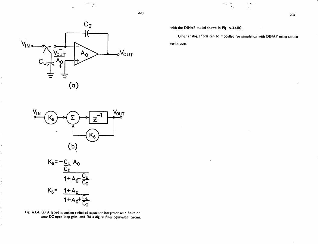
V,IN
K
(°)
Z
X
-1
(b)<5>
K5="CLi A0Ci
i +AJ-^.0 Ci
Kfi= 1+ Ai
ovqut
V,OUTo
223
Fig. A3.4. (a) A type-I inverting swiiched capacitor integrator with finite opamp DC open-loop gain, and (b) a digital filter equivalent circuit.
224
with ihe DINAP model shown in Fig. A.3.4(b).
Other analog effects can be modelled for simulation with DINAP using similar
techniques.

225
REFERENCES
[1] R.A. Friedenson, R.W. Daniels, R.J. Dow, and P.H. McDonald, "RC active
filters for the D3 channel bank," Bell System Technical Journal, vol. 54, no. 3,
pp. 507-529, March 1975.
[2] K.S. Tan and P.R. Gray, "Fully integrated analog filters using Bipolar/JFET
technology," IEEE J. Solid-State Circuits, vol. SC-13, pp. 814-821,
December 1978.
[3] D.D. Buss, D.R. Collins, W.H. Bailey, and CR. Reeves, "Transversal filtering
using charge transfer devices," IEEE J. Solid-State Circuits, vol. SC-8,
pp. 138-146, April 1973.
[4] R.D. Baertsch, W.E. Engeler, H.S. Goldberg, CM. Puckette, and
J.J. Tiemann, "The design of practical charge-transfer transversal filters," IEEE
Trans. Electron Devices, vol. ED-23, pp. 133-142, February 1976.
[5] C.H. Sequin, "Antialiasing inputs for charge-coupled devices," IEEE J. Solid-
State Circuits, vol. SC-12, pp. 609-616, December 1977.
[6] D.L. Fried, "Analog sampled data fillers," IEEE J. Solid-Slate Circuits,
vol. SC-7, pp. 302-304, August 1972.
[7] A. Fettweis, "Theory of resonant transfer circuits," Adv. Study Institute on
Network and Switching Theory, Italy, September 1966.
[8] K. Hirano and S. Nishimura, "Active RC filters containing periodically
operated switches," IEEE Trans, on Circuit Theory, May 1972.
[9] L.R. Rabiner and B. Gold, Theory and Application of Digital Signal Processing,
Prentice-Hall, Inc., Chap. 2, 1975.
226
[10] A.V. Oppenheim and R.W. Schafer, Digital Signal Processing, Prentice-Hall,Inc., Chap. 4, 1975.
[11] I.A. Young, P.R. Gray and D.A. Hodges, "Analog NMOS sampled data recur
sive filters," Digest Int. Solid-Slate Circuits Conf. (Philadelphia), pp. 156-157,
February 1977.
[12] R.C. Agarwal and CS. Burrus, "New recursive digital filter structures having
very low sensitivity and roundoff noise," IEEE Trans, onCircuits and Systems,
vol. CAS-22, no. 12, pp. 921-927, December 1975.
[13] B.J. Hosticka, R.W. Brodersen and P.R. Gray, "MOS sampled data recursive
fillers using state variable techniques," Proc. Int. Symp. on Circuits and Sys
tems (Phoenix), pp. 525-529, April 1977.
[14] B.J. Hosticka, R.W. Brodersen and P.R. Gray, "MOS sampled data recursive
filters using switched capacitor integrators," IEEE J. Solid-State Circuits,
vol. SC-12, pp. 600-608, December 1977.
[15] J.T. Caves, M.A. Copeland, CF. Rahim, and S.D. Rosenbaum, "Sampled ana
log filtering using switched capacitors as resistor equivalents," IEEE J. Solid-
State Circuits, vol. SC-12, pp. 592-599, December 1977.
[16] H.J. Orchard, "Inductorless filters," Electronic Letters, vol. 2, pp. 224-225,June 1966.
[17] K.R. Laker, M.S. Ghausi and J.J. Kelly, "Minimum sensitivity active (leapfrog)
and passive ladder bandpass filters," IEEE Trans, on Circuits and Systems,
vol. CAS-22, pp. 670-677, August 1975.
[18] F.E.J. Girling, and E.F. Good, "Applications of active ladder synthesis," Wire
less World, pp. 445-450, September 1970.

227
[19] G. Szeniirmai, "Synthesis of multi-feedback active fillers," Bell System Techni
cal Journal, pp. 527-555, April 1973.
[20] W.E. Heinlein and W.H. Holmes, Active Filters for Integrated Circuits, Prentice-
Hall International, Inc., Chap. 8, 1974.
[21] J.L. McCreary and P.R. Gray, "All-MOS charge redistribution analog-lo-digital
conversion techniques-part I," IEEE J. Solid-State Circuits, vol. SC-10, no. 6,
pp. 371-379, December 1975.
[22] R.E. Suarez, P.R. Gray and DA. Hodges, "All-MOS charge redistribution
analog-to-digital conversion techniques-part II," IEEE J. Solid-State Circuits,
vol. SC-10, no. 6, pp. 379-385, December 1975.
[23] G. Smarandoiu, "Nonlinear converters for pulse-code-modulation systems,"
Ph.D. Thesis, ERL Memo No. UCB/ERL M78/27, Electronics Research
Laboratory, University of California, Berkeley, CA, May 1978.
[24] D.J. Allslot, R.W. Brodersen and P.R. Gray, "Fully-integrated high order
NMOS sampled data ladder filters," Digest Int. Solid-State Circuits Conf. (San
Francisco), pp. 82-83, February 1978.
[25] D.J. Allstot, R.W. Brodersen and P.R. Gray, "MOS switched capacitor ladder
filters," IEEE J. Solid-Stale Circuits, vol. SC-13, pp. 806-814, December 1978.
[26] A.I. Zverev, Handbook of Filter Synthesis, John Wiley and Sons, Inc., New
York, 1967.
[27] G.C Temes and J.W. LaPatra, Introduction to Circuit Synthesis and Design,
McGraw-Hill Book Co., New York, 1977.
[28] DINAP-A Digital Network Analysis Program, Dept. of Electrical Engineering
and Computer Sciences, Purdue University, Layfayette, Indiana.
226
[29] Harry H-F Lam, Analog and Digital Filters: Design and Realization, unpublished
manuscript, July 1976.
[30] E. Cohen, "Program Reference for SP1CE2," ERL Memo No. ERL-M592,
Electronics Research Laboratory, University of California, Berkeley, CA,
June 1976.
[31] R. Easton, private communication.
[32] K.S. Tan, private communication.
[33] P.R. Gray, private communication.
[34] G. Kelson, H.H. Slellrecht, and D.S. Perloff, "A monolithic subsystem for
high-accuracy A/D conversion," IEEE J. Solid-State Circuits, vol. SC-8,
pp. 396-403, December 1973.
[35] E.l. Jury, Theory and Application of the Z-Transform Method, John Wiley and
Sons, Inc., New York, 1964.
[36] C.F. Kurth and G.S. Moschytz, "Two-port analysis of cascaded switched capaci
tor networks," IEEE Trans on Circuits and Systems. (To be published).
[37] Y.P. Tsividis, "Experimental and analytical evaluation of a swiiched capacitor
filter and remarks on the resistor/switched capacitor correspondence," IEEE
Trans, on Circuits and Systems. (To be published).
[38] G.M. Jacobs, D.J. Allsioi, R.W. Brodersen and P.R. Gray, "Design considera
tions for MOS switched capacitor ladder filters," Proc. Int. Symp. on Circuits
and Systems (New York), pp. 324-329, May 1978.
[39] G.M. Jacobs, D.J. Allstot, R.W. Brodersen and P.R. Gray, "Design techniques
for MOS switched capacitor ladder fillers," IEEE Trans, on Circuits and Sys
tems, vol. CAS-25, pp. 1014-1021, December 1978.
229
1401 L.T. Bruton, F.N. TrofimenkorT and D.H. Treleaven, "Noise performance of
low-sensilivity active filters," IEEE J. Solid-Slale Circuits, vol. SC-8, pp. 85-91,
February 1973.
(41 ] G.M. Jacobs, "Practical design considerations for MOS swiiched capacitor
ladder fillers," ERL Memo No. UCB/ERL M77/69, Electronics Research
Laboratory, University of California, Berkeley, CA, November 1977.
[42] L.T. Bruton, "Low Sensitivity digital ladder fillers," IEEE Trans, on Circuits
and Systems, vol. CAS-22, no. 3, pp. 168-176, March 1975.
[43] D.E. Johnson, Introduction to Filter Theory, Prentice-Hall International, Lon
don, 1976.
(441 A.A. Ibrahim, G.J. Hupe and T.G. Foxall, "Double-split-Eleclrode transversal
filter for telecommunications applications," IEEE J. Solid-State Circuits,
February 1979. (To be published).
|45] P.R. Gray, private communication.
(461 D.J. Allstot, R.W. Brodersen and P.R. Gray, "Considerations for MOS imple
mentations of switched capacitor filters," Asilomar Conference on Circuits,
Systems and Computers, PacificGrove, CA., November 1978.
147] D. Senderowicz, P.R. Gray and D.A. Hodges, "High performance depletion-
load NMOS operational amplifier," IEEE J. Solid-State Circuits, vol. SC-13,
pp. 760-766, December 1978.
(48) K.S. Tan, private communication.
[49] D.A. Vaughn-Pope and L.T. Bruton, "Transfer function synthesis using gen
eralized doubly-terminated two-pair networks," IEEE Trans, on Circuits and
Systems, vol. CAS-24, pp. 79-88, February 1977.
230
[50] S.K. Miira and R.J. Sherwood, "Digital ladder networks," IEEE Trans, on
Audio and Electroacoustics, vol. AU-21, pp. 30-36, February 1973.
151] W.C. Black, Jr., D.J. Allstot and R.P. Thiels, "Low-power CMOS monolithic
swiiched capacitor PCM fillers," (To be published).
(521 B.J. White, G.M. Jacobs and G.F. Landsburg, "Fully-integrated DTMF
receiver." Digest of the Int. Solid-State Circuits Conf. (Philadelphia. Pa.),
pp. 36-37, February 1979.
153] B.J. Hosticka, "MOS sampled data recursive fillers using state variable tech
niques," ERL Memorandum No. ERL-M77/65, Electronics Research Labora
tory, University of California, Berkeley, CA, August 1977.
(54] l.A. Young, "MOS switched-capaciior analog sampled-data recursive filters,"
Ph.D. Thesis, Memorandum No. UCB/ERL M78/61, Electronics Research
Laboratory, University of California, Berkeley,CA, November 1978.
(55] R.W. Brodersen, private communication.
(561 P.R. Gray, D. Senderowicz, H. O'Hara, and B.W. Warren, "A single-chip
NMOS dual channel filter for PCM telephony applications," ISSCC Digest of
Technical Papers (Philadelphia), pp. 26-27, February 1979.
(57) CR. Hewes, privatecommunication.
(58) J. L. McCreary, "Successive Approximation Analog-to-Digital Conversion
Techniques in MOS Integrated Circuits," Ph.D. Thesis, University of Califor
nia, Berkeley, 1975.
(591 D. J. Allslot, R. W. Brodersen, and P. R. Gray, "An electrically programmable
analog NMOS second-order filter," Digest of the Int. Solid-Stale Circuits Conf.
(Philadelphia), pp. 76-77, February 1979.

231
[60] W. J. Kerwin, L. P. Iluelsman and R. W. Newcomb, "Slate-variable synthesis
for insensitive circuit transfer functions," IEEE J. Solid-State Circuits,
vol. SC-2, pp. 87-92, September 1967.
[61] D. J. Allstot, R. W. Brodersen and P. R. Gray, "A digitally programmable ana
log NMOS switched capacitor filter," IEEE J. Solid-State Circuits,
December 1979. (To be published).
(62]. L. R. Rabiner and R. W. Schafer, Digital Processing of Speech Signals, Prentice-
Hall, Inc.. New York. 1978.
(63] T. Tsuda, G. Evancoe, et al, "A formant speech synthesizer using MOS/LSI
technology," (To be published).
164] R. W. Brodersen, P. R. Gray and D. A. Hodges, "MOS switched capacitor
filters," Proceedings of the IEEE, January 1979.
165] R. G. Meyer, "Nonlinear analog integrated circuits," EECS 240 class notes,
University of California, Berkeley, 1976.
(66) K. Martin and A. Sedra, "Designing leapfrog and SFG filters with optimum
dynamic range," Proceeding of the IEEE (letter), vol. 65, pp. 1210,
August 1977.
(67) R. W. Brodersen, private communication.