copyright by biying xu 2019
TRANSCRIPT

Copyright
by
Biying Xu
2019

The Dissertation Committee for Biying Xucertifies that this is the approved version of the following dissertation:
Layout Automation for Analog and Mixed-Signal
Integrated Circuits
Committee:
Zhigang (David) Pan, Supervisor
Nan Sun
Nur A. Touba
Michael Orshansky
Eric Soenen

Layout Automation for Analog and Mixed-Signal
Integrated Circuits
by
Biying Xu
DISSERTATION
Presented to the Faculty of the Graduate School of
The University of Texas at Austin
in Partial Fulfillment
of the Requirements
for the Degree of
DOCTOR OF PHILOSOPHY
THE UNIVERSITY OF TEXAS AT AUSTIN
May 2019

Dedicated to my parents and my grandmother.

Acknowledgments
I would like to express my deepest appreciation to my advisor, Professor
David Z. Pan, for his invaluable guidance and support throughout my Ph.D.
study. Professor Pan played a decisive role in leading me to solve critical and
challenging research problems independently in the field of electronic design
automation. He also provided generous suggestions in terms of technical writ-
ing and presentations that benefited me to a great extent. Besides, he helped
me connect with several internship opportunities where I have gained valuable
industrial experiences. For me, Professor Pan is not only a wise, patient, en-
couraging, and inspiring research advisor, but also a kind friend in the daily
life who has given me insightful advice. I am very fortunate to have worked
with him and learned much from him.
I would also like to extend my deepest gratitude to other committee
members for their precious efforts and contributions to this dissertation. In
particular, I very much appreciate Professor Nan Sun for the great number of
helpful discussions and collaborations on various research projects, where he
offered practical advice with his extensive knowledge of analog/mixed-signal
circuit design. I wish to express my sincere thanks to Professor Nur A. Touba
for his valuable comments and generous support during the development of
this dissertation. I am very grateful to Professor Michael Orshansky for his
v

constructive technical suggestions which contribute to the completeness of this
dissertation. I want to thank Dr. Eric Soenen for the comments and discus-
sions, as well as the generous support to the TSMC University Shuttle Program
for chip fabrication.
Besides, I am very grateful to other industrial mentors and collabo-
rators. Many thanks to Dr. Dennis Huang, Dr. Jian Kuang, Mr. Anurag
Tomar, and Dr. Vassilios Gerousis at Cadence Design Systems Inc. for their
active discussions on electronic design automation algorithms, practical advice
on programming skills, and continuous help throughout my internship there.
I am also very thankful to Dr. Ming Su and Dr. Bulent Basaran at Synop-
sys Inc., from whom I have received generous support and insightful guidance
during my internships at Synopsys.
I wish to thank the other alumni and members of the University of
Texas at Austin Design Automation Lab: Dr. Bei Yu, Dr. Subhendu Roy, Dr.
Xiaoqing Xu, Dr. Yibo Lin, Dr. Shaolan Li, Dr. Jiaojiao Ou, Dr. Derong
Liu, Dr. Meng Li, Shounak Dhar, Wuxi Li, Zheng Zhao, Wei Ye, Jingyi Zhou,
Mohamed Baker Alawieh, Che-Lun Hsu, Keren Zhu, Mingjie Liu, Rachel S.
Rajarathnam, Ahmet F. Budak, Zixuan Jiang, Jiaqi Gu, Joydeep Mitra, etc. It
has been my great pleasure working with them. The productive collaborations
and inspiring discussions with them, along with their constructive suggestions,
are particularly helpful to shape and polish this dissertation. Also, I cannot
leave UT without acknowledging the UT ECE staff, especially Melanie Gulick
and Andrew Kieschnick, for their continuous support in the administrative
vi

and IT issues which smooth the path for my research. In addition, I am lucky
to have met Poulami Das, my dear friend at UT, with whom the discussions
benefited me both personally and professionally. I am also very appreciative to
my other co-authors, teachers, and friends who helped in my study or research,
too.
Finally, I cannot begin to express my thanks to my dear family. Many
thanks to all of my family members who offer support and encouragements.
Mainly, I am thankful to my sister and best friend, Biyao Xu, for giving
me a considerable amount of love, warmth, and understanding. I am deeply
indebted to my father Zhiliang Xu and my mother Yanyun Xu, for their un-
conditional love. They teach me diligence, integrity, and the importance of
education. Besides, they strongly believe in my abilities even when I was dis-
couraged, and never waver in their support for everything I pursue. With
much love, I thank my parents for seeing me through all the hardship and
sharing every achievement along my Ph.D. study journey. Last but not least,
I would like to express my special appreciation to my grandmother Lan Tan.
Unfortunately, our family lost her. May she rest in peace. She had devoted
much time to nurturing me and profoundly impacted me with her merits, and
I believe her blessings will always be with me in whatever I do.
vii

Layout Automation for Analog and Mixed-Signal
Integrated Circuits
Publication No.
Biying Xu, Ph.D.
The University of Texas at Austin, 2019
Supervisor: Zhigang (David) Pan
Recently, the demand for analog and mixed-signal (AMS) integrated
circuits (ICs) has increased significantly due to various emerging applications.
However, most of the AMS IC layout design efforts are still handled manually
at present, which is time-consuming and error-prone. The AMS layout au-
tomation level is far from meeting the need for fast layout-circuit performance
iterations to accommodate the rapid growth of the market. In general, the
methodologies adopted by AMS layout automation tools mainly fall in several
different categories: (1) optimization-based approach, which is the most widely
used one; (2) template-based approach (e.g., for layout retargeting); and (3)
standard cell-based digitalized AMS circuit design and synthesis methodol-
ogy, which is a new direction preferable in advanced process technology nodes.
This dissertation proposes a set of techniques and algorithms to address var-
ious practical problems in these major directions of analog and mixed-signal
circuit layout automation research.
viii

For the direction of the optimization-based AMS IC layout automation,
two analog placement algorithms are proposed to improve the layout results
from different aspects. Firstly, hierarchical placement techniques for high-
performance AMS ICs are proposed, which minimize the critical parasitics in
addition to the total area and half-perimeter wirelength, while satisfying the
analog placement constraints simultaneously, including symmetry and proxim-
ity group constraints. Secondly, an analytical framework is proposed to tackle
the device layer-aware analog placement problem, which can effectively re-
duce the total area and wirelength without degrading the circuit performance,
leveraging the fact that it can be beneficial to overlap some devices built by
mutually exclusive layers.
For the direction of the template-based approach, this dissertation also
proposes a new layout retargeting framework. It first applies effective algo-
rithms to extract analog placement constraints from previous quality-approved
layouts, including symmetry and regularity constraints. After that, it preserves
the prior design expertise during retargeting while exploring different layout
topologies to improve the result quality.
Furthermore, for both optimization-based and template-based AMS IC
layout automation approaches, well island generation persists as a fundamental
and unresolved challenge in the post-placement optimization stage. To address
the well generation problem, this dissertation proposes a generative adversarial
network (GAN) guided framework with a post-refinement stage to mimic the
behavior of experienced designers in well generation, leveraging the previous
ix

high-quality manually-crafted layouts. Guiding regions for the well islands are
first generated by a trained GAN model, after which the results are legalized
through post-refinement to satisfy the design rules.
Finally, for the standard cell-based digitalized AMS IC design and syn-
thesis methodology, this dissertation presents a scaling compatible, synthesis
friendly ring voltage-controlled oscillator (VCO) based ∆Σ analog-to-digital
converter (ADC). Its circuit performance improves as process technology ad-
vances, and its layout can be fully synthesized by leveraging digital circuit
automation tools. It also demonstrates favorable performance compared with
the prior digitalized ADCs and in-line performance with state-of-the-art man-
ual designs.
x

Table of Contents
List of Tables xv
List of Figures xvii
Chapter 1. Introduction 1
1.1 Analog/Mixed-Signal Integrated Circuit Layout Design Au-tomation Problem . . . . . . . . . . . . . . . . . . . . . . . . . 2
1.2 Evolution of Analog/Mixed-Signal IC Layout Automation . . . 3
1.3 Analog/Mixed-Signal IC Layout Automation Challenges . . . . 5
1.4 Overview of this Dissertation . . . . . . . . . . . . . . . . . . . 7
Chapter 2. Hierarchical and Analytical Placement Techniquesfor High-Performance Analog Circuits 10
2.1 Introduction . . . . . . . . . . . . . . . . . . . . . . . . . . . . 10
2.2 Problem Formulation . . . . . . . . . . . . . . . . . . . . . . . 16
2.3 Hierarchical Placement Framework . . . . . . . . . . . . . . . . 19
2.3.1 Hierarchical Circuit Partitioning . . . . . . . . . . . . . 20
2.3.2 Hierarchical and Analytical Placement . . . . . . . . . . 23
2.3.2.1 Solving Placement Subproblems . . . . . . . . . 24
2.3.2.2 Parallelization . . . . . . . . . . . . . . . . . . . 27
2.4 Experimental Results . . . . . . . . . . . . . . . . . . . . . . . 28
2.4.1 Critical Parasitics Minimization . . . . . . . . . . . . . 30
2.4.1.1 Comparator Circuit . . . . . . . . . . . . . . . . 30
2.4.1.2 Ring Sampler Slice Circuit . . . . . . . . . . . . 31
2.4.2 Comparisons on Different Multiple Objectives Optimiza-tion Flavors . . . . . . . . . . . . . . . . . . . . . . . . . 34
2.4.3 Comparisons with Previous Work . . . . . . . . . . . . . 36
2.5 Summary . . . . . . . . . . . . . . . . . . . . . . . . . . . . . . 37
xi

Chapter 3. Device Layer-Aware Analytical Placement for Ana-log Circuits 38
3.1 Introduction . . . . . . . . . . . . . . . . . . . . . . . . . . . . 38
3.2 Problem Definition . . . . . . . . . . . . . . . . . . . . . . . . 44
3.3 Device Layer-Aware Analog Placement . . . . . . . . . . . . . 45
3.3.1 Global Placement . . . . . . . . . . . . . . . . . . . . . 46
3.3.2 Legalization . . . . . . . . . . . . . . . . . . . . . . . . . 49
3.3.2.1 Constraint Graph Construction . . . . . . . . . 49
3.3.2.2 Symmetry-Aware Legalization . . . . . . . . . . 56
3.3.3 Detailed Placement . . . . . . . . . . . . . . . . . . . . 57
3.4 Experimental Results . . . . . . . . . . . . . . . . . . . . . . . 58
3.4.1 Effects of Device Layer-Awareness . . . . . . . . . . . . 59
3.4.2 Routability Verification . . . . . . . . . . . . . . . . . . 60
3.4.2.1 Analog Global Routing . . . . . . . . . . . . . . 60
3.4.2.2 Congestion Analysis . . . . . . . . . . . . . . . 61
3.4.3 Effectiveness of the Analytical Framework . . . . . . . . 63
3.5 Summary . . . . . . . . . . . . . . . . . . . . . . . . . . . . . . 64
Chapter 4. Analog Placement Constraint Extraction and Explo-ration with the Application to Layout Retargeting 65
4.1 Introduction . . . . . . . . . . . . . . . . . . . . . . . . . . . . 65
4.2 Overall Flow . . . . . . . . . . . . . . . . . . . . . . . . . . . . 69
4.3 Layout Constraint Extraction . . . . . . . . . . . . . . . . . . 70
4.3.1 Regularity Constraint Extraction . . . . . . . . . . . . . 70
4.3.1.1 Lookup Table Construction . . . . . . . . . . . 72
4.3.1.2 Sweep Line-Based Algorithm . . . . . . . . . . 75
4.3.1.3 Algorithm Analysis . . . . . . . . . . . . . . . . 84
4.3.2 Symmetry Constraint Extraction . . . . . . . . . . . . . 86
4.4 Constraint-Aware Placement . . . . . . . . . . . . . . . . . . . 87
4.5 Experimental Results . . . . . . . . . . . . . . . . . . . . . . . 90
4.5.1 Layout Constraint Extraction Results . . . . . . . . . . 90
4.5.2 Layout Retargeting Results . . . . . . . . . . . . . . . . 91
4.6 Summary . . . . . . . . . . . . . . . . . . . . . . . . . . . . . . 95
xii

Chapter 5. WellGAN: Generative-Adversarial-Network-GuidedWell Generation for Analog/Mixed-Signal CircuitLayout 97
5.1 Introduction . . . . . . . . . . . . . . . . . . . . . . . . . . . . 97
5.2 Preliminaries . . . . . . . . . . . . . . . . . . . . . . . . . . . . 101
5.3 The WellGAN Algorithm . . . . . . . . . . . . . . . . . . . . . 103
5.3.1 Overall Flow . . . . . . . . . . . . . . . . . . . . . . . . 104
5.3.2 Data Representation and Preprocessing . . . . . . . . . 104
5.3.3 GAN-based Well Guidance Generation . . . . . . . . . . 106
5.3.4 Post-Refinement . . . . . . . . . . . . . . . . . . . . . . 110
5.3.4.1 Rectilinearization . . . . . . . . . . . . . . . . . 110
5.3.4.2 Legalization . . . . . . . . . . . . . . . . . . . . 111
5.4 Experimental Results . . . . . . . . . . . . . . . . . . . . . . . 114
5.5 Summary . . . . . . . . . . . . . . . . . . . . . . . . . . . . . . 119
Chapter 6. A Scaling Compatible, Synthesis Friendly VCO-based Delta-sigma ADC Design and SynthesisMethodology 121
6.1 Introduction . . . . . . . . . . . . . . . . . . . . . . . . . . . . 121
6.2 Circuit Design . . . . . . . . . . . . . . . . . . . . . . . . . . . 126
6.2.1 Preliminary of Delta-sigma ADC . . . . . . . . . . . . . 126
6.2.2 Proposed Synthesis Friendly Delta-sigma ADC . . . . . 126
6.2.2.1 Novel Synthesis Friendly TD Analog ComparatorDesign . . . . . . . . . . . . . . . . . . . . . . . 129
6.2.2.2 Synthesis Friendly DAC Architecture Selection . 131
6.3 Synthesis Methodology . . . . . . . . . . . . . . . . . . . . . . 132
6.3.1 Standard Cell Library Modification . . . . . . . . . . . . 133
6.3.2 HDL Generation . . . . . . . . . . . . . . . . . . . . . . 134
6.3.3 Floorplan Generation . . . . . . . . . . . . . . . . . . . 136
6.4 Experimental Results . . . . . . . . . . . . . . . . . . . . . . . 138
6.4.1 Comparisons in Different Process Technology . . . . . . 139
6.4.2 Comparisons with Previous Works . . . . . . . . . . . . 142
6.4.3 Measurement Results . . . . . . . . . . . . . . . . . . . 144
6.4.4 Analysis of Circuit and Layout Nonidealities . . . . . . 147
6.5 Summary . . . . . . . . . . . . . . . . . . . . . . . . . . . . . . 149
xiii

Chapter 7. Conclusion and Future Work 151
Bibliography 154
Vita 171
xiv

List of Tables
2.1 Notations for the high-performance analog circuit placementproblem. . . . . . . . . . . . . . . . . . . . . . . . . . . . . . . 15
2.2 Benchmark circuits. . . . . . . . . . . . . . . . . . . . . . . . . 29
2.3 Comparisons with and without minimizing critical parasitics ofcomparator circuit. . . . . . . . . . . . . . . . . . . . . . . . . 31
2.4 Simulation results of our placement and the manual layout ofring sampler circuit. . . . . . . . . . . . . . . . . . . . . . . . 34
2.5 Comparisons of different MOO flavors w/o considering criticalparasitics (run-time of each flavor: 100 s). . . . . . . . . . . . . 35
2.6 Comparisons of different MOO flavors considering critical par-asitics (run-time of each flavor: 100 s). . . . . . . . . . . . . . 36
2.7 Comparisons with state-of-the-art analog placement work. . . 37
3.1 Post-layout simulation results of the CC-OTA circuit. . . . . . 40
3.2 Post-layout simulation results of the CCO circuit. . . . . . . . 40
3.3 Benchmark circuits information. . . . . . . . . . . . . . . . . . 59
3.4 Results of our analytical analog placement framework (NLP). 60
3.5 Global routing (GR) results for the proposed analytical place-ment framework (NLP). . . . . . . . . . . . . . . . . . . . . . 62
3.6 Results of MILP-based placement with quality matching(MILP-Q) our framework without device layer-awareness (NLP). 62
3.7 Results of MILP-based placement with run-time matching(MILP-R) our framework without device layer-awareness (NLP). 63
4.1 Notations for layout constraint extraction. . . . . . . . . . . . 76
4.2 Benchmark AMS IC placements. . . . . . . . . . . . . . . . . . 90
4.3 Placement result comparison between the approach in [57] andour layout retargeting framework. . . . . . . . . . . . . . . . . 92
5.1 Statistics of the Manhattan norm of element-wise difference forthe test results. . . . . . . . . . . . . . . . . . . . . . . . . . . 119
xv

5.2 Post-layout simulation results of the op-amp layout with wellsgenerated by WellGAN. . . . . . . . . . . . . . . . . . . . . . 119
6.1 Example Verilog implementation of the proposed synthesisfriendly comparator. . . . . . . . . . . . . . . . . . . . . . . . 136
6.2 Example Verilog implementation of the proposed ADC slice. . 137
6.3 Performance comparison between 40-nm and 180-nm process. . 141
6.4 Comparisons with previous works. . . . . . . . . . . . . . . . . 144
6.5 Summary of measurement results. . . . . . . . . . . . . . . . . 148
6.6 Comparison with State-of-the-Art Manual Designed ADCs. . . 149
xvi

List of Figures
1.1 A typical analog/mixed-signal circuit design flow. . . . . . . . 2
2.1 (a) Example comparator circuit. (b) Transient simulations ofa comparator. Top: critical parasitics effects; Down: effects ofnon-critical ones. . . . . . . . . . . . . . . . . . . . . . . . . . 13
2.2 Example hierarchical symmetric constraints. . . . . . . . . . . 17
2.3 Hierarchical Analytical analog placement flow. . . . . . . . . . 19
2.4 Example hypergraph partitioning. . . . . . . . . . . . . . . . . 21
2.5 Example circuit hierarchy. . . . . . . . . . . . . . . . . . . . . 22
2.6 Hierarchical Analytical analog placement flow. . . . . . . . . . 23
2.7 Placement results of comparator circuit: (a) considers criticalnets, and (b) does not consider critical nets. Placement resultsof a slice of ring sampler circuit: (c) variant 1, and (d) variant 2. 32
3.1 CC-OTA circuit schematic and layout examples. . . . . . . . . 41
3.2 CCO circuit schematic and layout examples. . . . . . . . . . . 42
3.3 The overall flow of our device layer-aware analytical analogplacement engine. . . . . . . . . . . . . . . . . . . . . . . . . . 46
3.4 Example placement and constraint graphs. . . . . . . . . . . . 50
3.5 Placement with different device layers and its constraint graphs. 51
3.6 An example of the global placement result, and the constraintgraphs resulted from directly applying the plane sweep algo-rithm as in [14]. . . . . . . . . . . . . . . . . . . . . . . . . . . 51
3.7 The resulting constraints graphs generated by our algorithmafter resolving illegal overlaps, and after missing postional rela-tionship detection. . . . . . . . . . . . . . . . . . . . . . . . . 53
4.1 (a) The conventional analog layout retargeting framework. (b)The overall flow of the proposed analog layout retargetingframework. . . . . . . . . . . . . . . . . . . . . . . . . . . . . . 70
4.2 An example of AMS circuit placement. Orange: row constraint;Blue: column constraint; Red: array. . . . . . . . . . . . . . . 71
xvii

4.3 (a) The example analog placement in Figure 4.2 with the grids.(b) LUT Vdr and Hdr. (c) Vdl and Hdl. (d) Vlr and Hlr. . . . . 73
4.4 Applying Algorithm 4 to the placement in Figure 4.2 after pro-cessing VSLs 0 and 1. . . . . . . . . . . . . . . . . . . . . . . . 80
4.5 Applying Algorithm 4 to the placement in Figure 4.2 after pro-cessing VSL 2. . . . . . . . . . . . . . . . . . . . . . . . . . . . 81
4.6 Applying Algorithm 4 to the placement in Figure 4.2 after pro-cessing VSL 3. . . . . . . . . . . . . . . . . . . . . . . . . . . . 83
4.7 Applying Algorithm 4 to the placement in Figure 4.2 after pro-cessing VSL 4. . . . . . . . . . . . . . . . . . . . . . . . . . . . 83
4.8 Example placement with a mirror symmetry constraint. . . . . 87
4.9 Regularity constraints in benchmark #1. . . . . . . . . . . . . 91
4.10 Layout retargeting results of benchmark #1 by (a) [57], and (b)our appoach. . . . . . . . . . . . . . . . . . . . . . . . . . . . 93
4.11 Layout retargeting results of benchmark #2 by (a) [57], and (b)our appoach. . . . . . . . . . . . . . . . . . . . . . . . . . . . 93
4.12 Layout retargeting results of benchmark #3 by (a) [57], and (b)our appoach. . . . . . . . . . . . . . . . . . . . . . . . . . . . 94
4.13 Layout retargeting result area and run-time tradeoff of bench-mark (a) #1, (b) #2, and (c) #3. . . . . . . . . . . . . . . . . 95
5.1 Op-amp circuit example. . . . . . . . . . . . . . . . . . . . . . 100
5.2 Op-amp layout example. . . . . . . . . . . . . . . . . . . . . . 101
5.3 A typical back-end design flow for AMS circuits. . . . . . . . . 102
5.4 Proposed well generation framework (WellGAN). . . . . . . . 105
5.5 Architecture of a conventional GAN. . . . . . . . . . . . . . . 108
5.6 Architecture of a CGAN. . . . . . . . . . . . . . . . . . . . . . 109
5.7 (a) Conventional encoder-decoder architecture, and (b)Encoder-decoder with U-Net-like skip connections. . . . . . . . 110
5.8 Example post-refinement results after each step. . . . . . . . . 113
5.9 Grid-based method for the minimum width rule legalization. . 114
5.10 Test circuit examples A, B, C, and D. . . . . . . . . . . . . . . 118
5.11 Distribution of the Manhattan norm of the element-wise differ-ence. . . . . . . . . . . . . . . . . . . . . . . . . . . . . . . . . 119
6.1 (a) Power supply and transistor intrinsic gain scaling trend. (b)fT and FO4 delay trend. . . . . . . . . . . . . . . . . . . . . . 123
xviii

6.2 (a) Conventional VD-AMS circuits design flow. (b) Novel syn-thesis friendly TD-AMS circuits design flow. . . . . . . . . . . 124
6.3 Block diagram of a ∆Σ ADC. . . . . . . . . . . . . . . . . . . 126
6.4 The proposed scaling compatible, synthesis friendly VCO-based∆Σ ADC architecture. . . . . . . . . . . . . . . . . . . . . . . 128
6.5 (a) Transistor level schematic of VCO cell. (b) VCO imple-mented using digital inverters gates. . . . . . . . . . . . . . . . 128
6.6 (a) Regular TD comparator. (b) TD comparator by connectingtwo 3-input NOR gates. . . . . . . . . . . . . . . . . . . . . . 130
6.7 (a) Proposed TD comparator gate-level implementation withSR-latch. (b) A conventional current-steering DAC. (c) Theresistor DAC used in our synthesis friendly ADC circuit. . . . 131
6.8 Overall flow of the layout synthesis methodology for the pro-posed synthesis friendly ADC. . . . . . . . . . . . . . . . . . . 133
6.9 (a) Standard cell library modification. (b) Floorplan generation. 135
6.10 Generated resistors standard cells layouts: (a) 1 kΩ resistor withlower resistivity. (b) 11 kΩ resistor with higher resistivity. . . . 136
6.11 One slice of the ADC decomposed into different power domainsand floorplan groups. . . . . . . . . . . . . . . . . . . . . . . . 138
6.12 Automatically synthesized layouts in: (a) 40-nm CMOS pro-cess. (b) 180-nm CMOS process. (c) Automatically synthe-sized layout in 40-nm CMOS process with power domains andcomponents groups indicated. . . . . . . . . . . . . . . . . . . 140
6.13 Power Breakdown of our ADC circuit in (a) 40-nm CMOS pro-cess. (b) 180-nm CMOS process. . . . . . . . . . . . . . . . . 142
6.14 Post-layout transient simulation results of the ADC time-domain outputs in: 40-nm CMOS process (left), and 180-nmCMOS process (right). . . . . . . . . . . . . . . . . . . . . . . 142
6.15 Post-layout simulation results of the ADC spectrum in: 40-nmCMOS process (left), 180-nm CMOS process (right). . . . . . 143
6.16 ADC spectrum and time-domain output with low input ampli-tude in 40-nm CMOS process. . . . . . . . . . . . . . . . . . . 143
6.17 Fabricated chip die photograph. . . . . . . . . . . . . . . . . . 145
6.18 Measured output spectrum. . . . . . . . . . . . . . . . . . . . 145
6.19 Measured SNDR across multiple chips. . . . . . . . . . . . . . 146
6.20 Measured SNDR/SNR vs. input amplitude. . . . . . . . . . . 147
xix

Chapter 1
Introduction
Analog and mixed-signal (AMS) integrated circuits (ICs) are used
widely and heavily in many emerging applications, including Internet of Things
(IoT), communication and 5G networks, advanced computing, automotive
electronics in electric and autonomous vehicles, healthcare electronics, etc.
The increasing demand for these applications necessitates a shorter design cy-
cle and time-to-market of AMS ICs. However, the AMS IC layout automation
level is far from meeting the need for fast layout-circuit performance iterations
to accommodate the rapid growth of the market, lagging far behind their dig-
ital counterparts that are relatively mature. Most of the layout design efforts
in AMS ICs are still handled manually. This is time-consuming and error-
prone, especially as the design rules are becoming increasingly complicated in
nanometer-scale IC era, and as the circuit performance requirements are be-
coming more and more stringent. Despite the progress in the AMS IC layout
design automation field [39,50,59,72,83], the automated layout tools have not
been widely used among the layout designers. There are still practical prob-
lems remaining to be solved in the AMS IC layout automation field. Hence, it
is necessary to develop effective and efficient design automation tools for AMS
ICs.
1

Analog Placement
Post-Placement Opt.
Post-Routing Opt.
Layout
Analog Sizing
Circuit Spec.
Architecture & Topology Selection
Analog Routingback-end
front-end
Spec. Met? NY
Spec. Met?N
Y
Figure 1.1: A typical analog/mixed-signal circuit design flow.
1.1 Analog/Mixed-Signal Integrated Circuit LayoutDesign Automation Problem
The typical design flow of AMS ICs can be generally shown in Fig-
ure 1.1. It consists of front-end design stages and back-end stages. For the
front-end circuit design, the appropriate circuit architecture and topology are
first selected to meet the circuit performance specifications. Then, device siz-
ing is determined according to the empirical calculation, rigorous simulations,
or numerical methods [16,24,48].
The back-end layout stages mainly include analog placement and rout-
ing. They are different from their digital counterparts, in that (1) the heights
2

of the devices could be different, and the placement typically does not follow
the row-based style; (2) various layout constraints may need to be satisfied,
e.g., symmetry, matching, coupling, etc.; (3) in addition to total area and
wirelength, the objectives of minimizing the post-layout circuit performance
degradation are often more important. Besides the placement and routing
core tasks, post-placement (e.g., well generation) and post-routing (e.g., net
shielding) optimization stages are also fundamental to optimize the circuit
performance.
Note that during the design process, if at any time the pre-layout or
post-layout simulations result in violations to the design specifications, either
previous stages will need to be revisited or the specs will need to be adjusted.
All the stages in the AMS IC design flow can be done manually or automat-
ically. The scope of this dissertation is in automating the back-end layout
design stages for AMS ICs.
1.2 Evolution of Analog/Mixed-Signal IC Layout Au-tomation
In general, the methodologies adopted by AMS IC layout automa-
tion tools mainly fall in the following different categories or directions: (1)
optimization-based approach; (2) template-based method; and (3) standard
cell-based digitalized AMS circuit design and synthesis methodology. The
early endeavors of analog layout generation also included procedural approach
(e.g., ALSYN [106]), where the designer codified the entire layout, and the
3

tool would generate the design accordingly. This approach relies heavily on
the circuit designer’s development, and thus the automation aspect is limited.
The optimization-based approach generates AMS IC layouts using op-
timization techniques with some cost functions. It is widely used among the
AMS IC layout automation tools. Most of the early works, including ILAC [78],
KOAN/ANAGRAM II [11], GELSA [75], Malavasi et al. [60], LAYLA [39],
applied simulated annealing for layout optimization. These works generally
explored an excessively large solution space and were thus time-consuming.
More recent works [26,43,45,47,50,59,72–74,83,94] focused on improving the
analog layout constraint handling and the design space pruning. However,
most of these prior works employed stochastic optimization methods (e.g.,
simulated annealing and genetic algorithms) or enumerative approach, which
still suffered from scalability and efficiency issues.
The template-based approach generates the placement and routing ac-
cording to the pre-defined relative positions (templates). It is usually used
for analog circuit layout retargeting or migration. IPRAIL [31], ALG [103],
Zhang et al. [105], Liu et al. [57], LAYGEN [58] and LAYGEN II [61] are a few
examples using this approach when generating analog layouts. Although the
template-based approach is fast, they usually lack the flexibility of optimizing
towards specific objectives. Therefore, it is more suitable when the circuit and
layout parameters are only changed slightly.
The standard cell-based digitalized AMS circuit design and synthesis
methodology is a relatively new trend leveraging the digital standard cells
4

to design the AMS circuit systems and using the digital circuit automatic
placement and routing (APR) tools to generate the layouts. Prior works have
demonstrated preliminary success with this design methodology in various
AMS circuit types, including ADCs [89–91], phase-locked loop (PLL) [13], and
filters [55]. It is especially preferable in advanced process technology nodes due
to the scaling benefits of the digital standard cells. By taking advantage of the
digital circuit APR tools, this approach can significantly enhance the run-time
efficiency of the AMS circuit layout process.
1.3 Analog/Mixed-Signal IC Layout Automation Chal-lenges
From the previous descriptions, we know that the AMS IC layout au-
tomation approaches are suitable for different tasks. Therefore, research efforts
are marching in these different directions simultaneously. However, despite the
continuing advancements, the research and development of AMS IC layout au-
tomation are still facing the following vital challenges.
Considerations of practical scenarios in AMS ICs. Currently,
the automated layout tools are still limited to consider the more practical
and complex scenarios of AMS ICs. For example, critical net parasitics min-
imization is vital to the high-performance analog ICs. Another characteristic
unique to AMS IC is that different devices built with different layers require co-
optimization in the layout. The AMS circuit layout automation would benefit
from comprehensively considering these characteristics.
5
Run-time scalability issue. The optimization-based methods using
stochastic optimization or enumeration are still not efficient enough in terms
of run-time to handle large-scale analog and mixed-signal systems. Also, when
being integrated into a closed-loop layout flow, it is necessary to develop fast
placement and routing algorithms to accommodate more iterations. Therefore,
more scalable algorithms are preferable.
Flexibility issue of template-based approach. As mentioned
above, the template-based approach is not flexible in exploring different lay-
out topologies, which could be undesirable when there are more substantial
changes to the circuit parameters. Hence, developing more flexible template-
based layout automation framework is needed.
Addressing the post-placement optimization problem. Al-
though the studies on analog placement and routing are relatively active, as
a fundamental step in the back-end flow, the post-placement optimization
is often neglected. In the advanced process technology nodes, the layout-
dependent effects are increasingly prominent. Therefore, post-placement opti-
mization step, including well generation, has a higher and higher influence on
the circuit performance.
Improving the performance of the standard cell-based AMS
circuit. The previous standard cell-based digitalized AMS circuits either still
require substantial manual layout efforts, or cannot achieve satisfactory circuit
performance. Consequently, it is crucial to design highly digitalized, synthesis-
friendly AMS IC with performance comparable to the state-of-the-art.
6

1.4 Overview of this Dissertation
This dissertation proposes a set of techniques and methodologies on
analog and mixed-signal integrated circuit layout automation to tackle various
challenges. The goal of this dissertation is to improve the quality and efficiency
of automatic layout design for AMS circuits.
For the direction of optimization-based AMS IC layout automation, two
automated analog placement algorithms are proposed to improve the layout
results from different aspects. In Chapter 2, a hierarchical placement frame-
work for high-performance analog circuits is proposed, which minimizes the
critical parasitics in addition to the total area and half-perimeter wirelength
(HPWL) while satisfying the analog placement constraints simultaneously, in-
cluding symmetry and proximity group constraints [99]. This hierarchical and
parallelized framework can reduce the post-layout circuit performance degra-
dation whereas keeping other objectives satisfactory. Then, in Chapter 3,
a holistic analytical framework is proposed to tackle the device layer-aware
analog placement problem, which can effectively reduce the total area and
wirelength without degrading the circuit performance, leveraging the fact that
some devices can be built by mutually exclusive layers and overlapping them
can be beneficial [97].
For the direction of the template-based approach, in Chapter 4, this
dissertation also proposes a new layout retargeting framework which applies
effective algorithms to extract analog placement constraints from previous
quality-approved layouts, including symmetry and regularity constraints, to
7

improve the layout quality while preserving prior design expertise [96]. A
novel sweep line-based algorithm is developed to extract the regularity con-
straints in a placement. It is demonstrated that the proposed framework is
able to reduce the placement area compared with the conventional approach.
Furthermore, for both optimization-based and template-based AMS IC
layout automation approaches, well island generation persists as a fundamen-
tal and unresolved challenge in the post-placement optimization stage. To
address this problem, Chapter 5 proposes a generative adversarial network
(GAN) guided well generation framework to mimic the behavior of experienced
designers in well generation, leveraging the previous high-quality manually-
crafted layouts [100]. Guiding regions for wells are first created by a trained
GAN model, after which the well generation results are legalized through an
effective post-refinement algorithm to satisfy the design rules following the
guidance of solutions generated by GAN.
For the standard cell-based digitalized AMS circuit design and lay-
out synthesis methodology, Chapter 6 presents a scaling compatible, synthesis
friendly ring voltage-controlled oscillator (VCO) based ∆Σ analog-to-digital
converter (ADC) design [42, 98]. Its layout is fully synthesized by leveraging
digital circuit automated placement and routing tools to reduce the layout
time, as it can be decomposed into digital gates and a small set of simple
customized cells. The circuit performance naturally improves as technology
advances. It is demonstrated to achieve favorable circuit performance and ex-
cellent scaling compatibility compared with the previous works of digitalized
8

ADCs. Its performance is in-line with the state-of-the-art manually designed
ADCs as well.
Finally, Chapter 7 summarizes and concludes this dissertation, and also
discusses the potential future research topics.
9

Chapter 2
Hierarchical and Analytical Placement
Techniques for High-Performance Analog
Circuits
This chapter first discusses the high-performance analog circuit place-
ment problem and solves it with a hierarchical framework which minimizes the
critical parasitics.
2.1 Introduction
With the expanding market share of emerging applications, including
consumer electronics, automotive, and Internet of Things (IoT), the demands
in analog and mixed-signal (AMS) integrated circuits (ICs) are becoming
higher and higher. The complexity explosion of the design rules and circuit
performance requirements in nano-meter IC era also dramatically increases the
complexity of their layouts. Hence, it is necessary to have design automation
tools for AMS ICs [46].
This chapter is based on the following publication: Biying Xu, Shaolan Li, Xiaoqing Xu,Nan Sun and David Z. Pan, “Hierarchical and Analytical Placement Techniques for High-Performance Analog Circuits, ” ACM International Symposium on Physical Design (ISPD),2017. I am the main contributor in charge of problem formulation, algorithm developmentand experimental validations.
10

One key goal and challenge in high-performance analog layout circuits
is the minimization of critical parasitics effects on the post-layout circuit per-
formance. Critical parasitics in analog design are the parasitics that would
trigger major impacts on key analog performance metrics when they vary.
The critical parasitics and their effects on performance are usually identified
by the analog circuit designers before starting layout, in order to efficiently
minimize the degradation of post-layout performance.
Without loss of generality, we can demonstrate the significance of crit-
ical parasitics management through a dynamic latch comparator, as shown in
Figure 2.1a. The parasitic capacitances that are of our interest are drawn,
where C ∗ (e.g. C OUTP ) indicates a net’s self-capacitance to substrate, and
CC ∗ (e.g. CC OUT ) indicates the coupling capacitance between two nets.
The speed of a comparator cannot be optimized simply through the minimiza-
tion of total wirelength, which may be over-emphasized by conventional analog
placement methodologies. In fact, it is only strongly related to certain capac-
itances which are called critical parasitic capacitances, while other parasitic
capacitances have much weaker or marginal effects on the speed. The critical
parasitics identified by the circuit designers are highlighted by the red boxes.
We perform simulations to show the difference in the effects caused by the
critical parasitics and non-critical ones. Simulation results of the comparator
transition waveform are shown in Figure 2.1b. In the simulation setting, the
capacitors are swept from 0 to 2 fF, which are typical values of parasitic capac-
itance in modern processes. It can be clearly seen that the capacitance loading
11

of the outputs (C OUTP and C OUTN) presents major impact (2x increase
in delay). On the other hand, other parasitic capacitances (e.g. C V G) have
much less impact on the comparator speed. Therefore, in terms of speed, the
parasitics on nodes OUTP and OUTN are the critical ones, while others can be
loosely managed. The wirelengths of OUTP and OUTN should be minimized
to reduce the self-parasitic capacitances.
From the above discussion, it can be seen that constraints in ana-
log design are net-specific. Conventional optimization techniques without
considering net-specific requirements become suboptimal in optimizing high-
performance analog circuits. High-performance analog layout synthesis re-
quires a critical net aware algorithm.
The work [69] used a branch-and-bound technique in the building block
layout problem to consider critical nets with maximum length constraints.
Their work considered maximum critical net length constraints for digital cir-
cuits rather than minimizing the critical parasitics for analog circuits. Another
prior work [39] proposed to first perform circuit analysis to determine the sen-
sitivity of circuit performance to each parasitic loading, and then optimize per-
formance degradation, among other metrics. However, exhaustive circuit anal-
ysis without taking advantage of the designer’s knowledge was time-consuming
and could potentially lead to inaccuracy. Proximity constraints have been used
to restrict some modules to be placed in close proximity [50, 59, 83, 87]. How-
ever, they did not impose net-specific requirements, and thus were not enough
to minimize critical parasitics. Boundary constraints were applied in [44] for
12

C_OUTN C_OUTP
CC_OUT
C_XP C_XN
C_VG
CC_XIP CC_XIN
INP INN
CLK
CLK CLK
OUTPOUTN
VDD
GND
(a)
OUTP
OUTNC_OUTN 0 1 fF 2 fF
C_OUTP 0 1 fF 2 fF
OUTN
OUTP
C_VG 0 -> 2 fF
(b)
Figure 2.1: (a) Example comparator circuit. (b) Transient simulations of acomparator. Top: critical parasitics effects; Down: effects of non-critical ones.
13

analog placement to reduce wiring parasitics, which were also insufficient be-
cause the devices may still be far away even if they are placed on the boundary
of a group. The work [95] considered monotonic current paths constraints to
reduce the routing-induced parasitics. Recently, [45] fully separated analog
and digital signal paths for noise reduction of AMS circuits. Nevertheless,
these heuristics did not minimize critical parasitic loading explicitly, either.
Analog circuit hierarchy has been taken into account during placement
previously by [45,62] which demonstrated the effectiveness of the hierarchical
approach. However, neither of them considered critical parasitics explicitly.
Meanwhile, topological approaches have been widely used to solve the analog
placement problem, including B* tree [50, 83], Corner Block List (CBL) [59],
Sequence Pair [49,51], Slicing Tree [93], etc. Nonetheless, they require a pack-
ing step before wirelength can be estimated, while absolute coordinates ap-
proaches [62, 72] could provide a more accurate estimation of wirelength by
construction.
Our main contributions are summarized as follows.
• We formulate the high-performance analog circuit placement problem
which minimizes the total area, half-perimeter wirelength (HPWL), and
critical parasitics simultaneously while accommodating analog placement
constraints.
• Since AMS circuits typically have the hierarchical structure, we propose
a hierarchical scheme for analog placement to honor the circuit hierarchy.
14

Table 2.1: Notations for the high-performance analog circuit placement prob-lem.
WL,CL the total HPWL and critical net HPWL.
W ,H the total width and height of the placement.
M the set of all devices/subpartitions.
w(k)i , h
(k)i
the width and height of the k-th variant of the i-thdevice/subpartition M
(k)i .
xi, yithe horizontal and vertical coordinates of the location of thei-th device/subpartition.
N,Nc the set of all nets and critical nets.
wli the HPWL of net i.
Sthe set of all hierarchical symmetric groups,S = S1, S2, · · · , Sm.
L the placement solution.
Asummation of the average area over all variants of thedevices/subpartitions, i.e. A =
∑i((
∑kiw
(ki)i · h(ki)i )/ki).
• The proposed hierarchical analog placement algorithm is parallelizable
and scalability is demonstrated.
• Experimental results show that circuit performance degradation is re-
duced by minimizing the critical parasitics while keeping other objectives
satisfactory.
The rest of this chapter is organized as follows: Section 2.2 gives the
problem formulation of the high-performance analog circuits placement prob-
lem. Section 2.3 proposes the hierarchical analog placement framework. Sec-
tion 2.4 shows the experimental results. Section 2.5 summarizes the chapter.
15

2.2 Problem Formulation
This section shows the formulation for the high-performance analog IC
placement problem. The notations we use are listed in Table 2.1.
Firstly, we give the optimization objectives of the placement problem
for high-performance analog ICs. As discussed in the previous section, the
performance of an analog circuit is strongly affected by the critical parasitics.
Several factors could affect parasitic capacitance of a net, e.g. net length, metal
overlap with other nets, spacing with other nets running in parallel with it,
etc. While the metal overlap and parallel spacing are often hard to control
in the placement stage, the critical net wirelength can be effectively mod-
eled by its HPWL during placement. Therefore, the total critical net HPWL
can be expressed as CL =∑
neti∈Ncwli, and total HPWL can be written as
WL =∑
neti∈N wli. The high-performance analog placement problem tries to
minimize CL in addition to the conventional optimization objectives of WL
and the total area A.
Secondly, we discuss how analog placement constraints are considered.
Practical analog layout designs typically contain hierarchical structure and
symmetric constraints. In a multi-level hierarchical structure, symmetric con-
straints may apply to subpartitions at each level, thus generating hierarchical
symmetric constraints, which we define as follows:
Definition 1 (Hierarchical Symmetric Constraint). A hierarchical symmetric
constraint is a placement constraint requiring at least one symmetric group to
16

31
26
7
8
5 10
H symmetric
V symmetric
H and V symmetric9
4
Figure 2.2: Example hierarchical symmetric constraints.
be symmetric to at least one other symmetric group or component, which forms
a new hierarchical symmetric group.
An example hierarchical symmetric constraint is illustrated in Fig-
ure 2.2. The blue boxes indicate symmetric constraints with horizontal axes
(H symmetric), the red boxes indicate those with vertical axes (V symmetric),
and the magenta boxes indicate those requiring both horizontal and vertical
symmetry (H and V symmetric). For instance, rectangles 1, 2, 3 form an
H symmetric group, where 1 and 2 form a symmetric pair and rectangle 3 is
self-symmetric with respect to the same axis as the symmetric pair 1, 2. The
V symmetric constraint in this example is a hierarchical symmetric constraint,
because it contains the H symmetric groups of 1, 2, 3 and 6, 7, 8 as a
hierarchical symmetric pair, and requires the H and V symmetric group of 5,
9, 10 and rectangle 4 to be self-symmetric in the mean time.
The previous work [50] mentioned the concept of hierarchical symmet-
ric constraints and discussed how they could be handled using hierarchical
symmetric feasible B* trees. However, no experiment has been done to demon-
17

strate the effectiveness of this technique for practical analog placement. In this
work, we consider hierarchical symmetric constraints in a hierarchical and ana-
lytical placement engine. Suppose Ml and Mr are any 2 devices/subpartitions
which form a symmetric pair in a vertical hierarchical symmetric group Sj,
and Mm is any self-symmetric device/subpartition in the same Sj. We have
xl + xr + wr = 2 · aj, and 2 · xm + wm = 2 · aj, where aj is the vertical
symmetric axis of Sj. The horizontal hierarchical symmetric constraints can
be written similarly. Furthermore, proximity constraints require some de-
vices/subpartitions to be in close proximity, which will be satisfied by con-
struction of the circuit hierarchy in our placement engine. A legal placement
also needs to satisfy the non-overlapping constraints which forbid overlap be-
tween any devices. Besides, orientation and variants selection will be addressed
by our analog placement engine.
Finally, the high-performance analog circuit placement problem can be
stated as follows:
Problem 1 (High-Performance Analog Placement). The high-performance
analog placement problem is to find legal device placement/s given the circuit
netlist and device variants in different sizes, which simultaneously minimizes
critical net wirelength, the total wirelength and area, while accommodating hi-
erarchical symmetric constraints, proximity constraints, and non-overlapping
constraints.
18

Hierarchical and Analytical Placement
Construct Circuit Hierarchical Structure
ProximityConstraints
Critical Nets
Hierarchical Symmetry
Constraints
Placement Results
Circuit NetlistInformation
Figure 2.3: Hierarchical Analytical analog placement flow.
2.3 Hierarchical Placement Framework
The overall flow of our hierarchical analytical placement algorithm for
high-performance analog circuits is shown in Figure 2.3. If the circuit hierarchy
is provided by the designer, our algorithm takes it as input directly. Other-
wise, we apply a critical parasitics aware, symmetric and proximity constraints
feasible hierarchical circuit partitioning technique. After the circuit hierarchy
is obtained, hierarchical and analytical placement is performed from bottom
up. Different placement subproblems at the same level in the circuit hierar-
chy are solved in parallel. MILP formulation is used to solve the placement
subproblems for all subpartitions.
19

2.3.1 Hierarchical Circuit Partitioning
Analog circuits are typically organized in a hierarchical manner. The
circuit hierarchy input by circuit designers often reflects their expertise and
insights, such as which components should be placed in close proximity to
avoid process variation induced circuit performance degradation, etc.
Also, placing the modules in the way designers partition the circuit
would increase the readability of the placement results by the designers. There-
fore, our analog placement engine will respect the circuit hierarchy if it is pro-
vided, as in [51, 68, 83]. Nevertheless, while the circuit designers have more
insights in electrical performance optimization, they may have difficulty op-
timizing geometrical metrics (e.g. area) and electrical performance simulta-
neously. Therefore, in addition to being able to take the circuit hierarchy as
an input, our analog placement engine will also be able to perform circuit
partitioning specific to analog circuits for geometrical and electrical metrics
co-optimization.
Although there are many existing well-established circuit partitioning
techniques [18, 41, 80, 101], they are not directly applicable to analog circuits
because of the analog placement constraints. However, we can adapt these
algorithms to follow the following guidelines to make it aware of the parasitic
loading and analog placement constraints:
• Modules in a hierarchical symmetric group should be in the same hier-
archical partition.
20

1
2 3
4 5
6
7 8
9
10
critical net
non-critical net
graph cut
Figure 2.4: Example hypergraph partitioning.
• Modules belonging to a proximity group should be in the same partition
(the proximity constraint is satisfied by construction).
• Different criticality of different parasitic capacitances could be reflected
by different net weights.
In this work, we adapted the hMetis [33] hypergraph partitioning al-
gorithm by specifying fixed module partitions and setting proper weights for
critical nets, with the implementation details clarified in Section 2.4. The en-
tire netlist is modeled by a hypergraph, which we call the top-level hypergraph,
where the placement devices (e.g. transistors) are its vertices and the nets are
its hyperedges. It is first partitioned following the high-performance analog
circuit partitioning guidelines above, and results in several subpartitions, each
of which is a sub-hypergraph of the top-level hypergraph. The internal hyper-
edges/nets of a sub-hypergraph are derived from the hyperedges of the top-
21

1 2 3
4 5
6 7 8
9 10
Level 1
Level 2
Level 3
Level 4
Figure 2.5: Example circuit hierarchy.
level hypergraph that connect only vertices within the sub-hypergraph. The
external hyperedges/nets are the those connecting different vertices in different
sub-hypergraphs. Similarly, each sub-hypergraph of the top-level hypergraph
is partitioned following the same guidelines, but now only the internal hyper-
edges will be considered. The partitioning continues hierarchically until the
desired number of placement devices are left in each leaf-level subpartition.
An example hierarchical partitioning of the circuit with hierarchical
symmetric constraints and critical nets is shown in Figure 2.4, and the con-
structed circuit hierarchy from this partitioning is as in Figure 2.5. Critical
nets of the circuit netlist are colored in red, and the others in black are non-
critical nets. This example circuit has hierarchical symmetric constraints as
in Figure 2.2. While the partitioning algorithm tries to avoid cutting critical
nets, it may still do so if much better area balance could be achieved or if other
ways of partitioning cannot satisfy the hierarchical symmetric constraints or
22

top-block
sub-partition
1
device 1
device 2
devicek
sub-partition
2
sub-partition
m
Level 1
Level 2
Level n
final placement
variants
varaintsin each sub-
partition
input varaints
Ordered
Parallel
Figure 2.6: Hierarchical Analytical analog placement flow.
proximity constraints for the desired number of partitions and desired number
of levels in the circuit hierarchy specified by the designers. An example of the
resulting circuit hierarchy for the example circuit is shown in Figure 2.5. In
this case, the partitioning algorithm first separates the H and V symmetric
group (in magenta) of 5, 9 10 and others into 2 subpartitions at the second
level. The other devices are further partitioned into 3 subpartitions of the H
symmetric groups of 1, 2, 3 and 6, 7, 8 and device 4 at the third level. A
subpartition may contain a single placement device as a special case.
2.3.2 Hierarchical and Analytical Placement
Given the circuit hierarchy constructed from the user input hierarchical
circuit netlist or from the proposed analog circuit partitioning, our placement
algorithm is illustrated in Figure 2.6.
23

The leaf nodes of the circuit hierarchy represent primitive placement
devices such as transistors or subcircuits that have been pre-laid out by the
designers, and the internal nodes (non-leaf nodes) indicates hierarchical parti-
tions. Each node in the hierarchy contains several variants, and exactly one of
them will be selected by the placement algorithm. For a leaf node, the variants
are inputs from the designers. For example, the variants of a transistor leaf
node are different layouts that can be considered electrically equivalent (with
the same transistor width and length) but have a different number of fingers
and thus different geometrical shapes (with different geometrical width and
height). For an internal node, the variants are the placement results for that
hierarchical partition, which have different bounding box shapes (with differ-
ent total widths and heights), different aspect ratios, and different locations,
orientations, or selected input variants for the devices. The different variants of
an internal node are generated by solving a placement subproblem of a subpar-
tition, which then propagate and become inputs to the placement subproblem
of its parent node. Different placement subproblems at different levels in the
circuit hierarchy are solved orderly from bottom-up, while those at the same
level can be solved in parallel. Finally, the different variants contained in the
root node are the set of placement results for the top-block.
2.3.2.1 Solving Placement Subproblems
Since the proximity constraints are satisfied during our construction
of the circuit hierarchy, the placement subproblem of a subpartition does not
24

need to handle these constraints. It is formulated as below:
Problem 2 (Placement Subproblem). Given a set of subpartitions each con-
taining different variants and the external nets connecting them, the high-
performance analog placement subproblem is to find legal placement/s of these
subpartitions which simultaneously minimizes the critical net wirelength and
total wirelength within these subpartitions and total area of them, while accom-
modating hierarchical symmetric constraints and non-overlapping constraints
among these subpartitions.
This is a multiple objectives optimization (MOO) problem, and gener-
ally, the optimal values of different objectives are usually not achieved at the
same solution. We say that a solution s of a MOO problem dominates another
solution s if s has better values for one or more objectives than s and the same
values for all other objectives as s. The aim of the high-performance analog
IC placement subproblem is to try to obtain the placement solutions that are
non-dominated by any other solution in terms of the objectives of critical net
wirelength, the total HPWL, total width and total height.
To solve each placement subproblem, first, a list of initial widths W (1)0 ,
W(2)0 , · · · ,W (r)
0 are calculated based on the desired initial aspect ra-
tios and total area by GetInitialWidths (Algorithm 1), where AR(i)0 =
(W(i)0 )/(H
(i)0 ), i = 1, · · · , r are the input initial aspect ratios by the design-
ers. The normalization factors can be obtained in different ways, e.g. by
H(i)0 = (W
(i)0 )/(AR
(i)0 ), and WL
(i)0 = (H
(i)0 +W
(i)0 )/2 ·n, where n is the number
25

of nets. Then, three approaches with different optimization flavors towards dif-
ferent objectives are explored which are shown in DifferentMOOFlavors (Al-
gorithm 2), each variating the general MILP problem as shown below, where
total width/height boundary constraints specify the placement boundaries:
minL
α · HH0
+ β · WW0
+ θ · WL +γ · CL
WL0
s.t. hierarchical symmetric constraints
non-overlapping constraints
total width/height boundary constraints
• SequentialMin finds a solution on the Pareto Front by sequentially min-
imizing H, W and the weighted sum of WL and CL. First, it minimizes
H given a specific W0 with MinHeightMILP by setting β and θ to 0 in
the general MILP, and the width boundary to W0. H indicates the re-
sulting optimal height, and L1 represents the placement result of this
step. Then, it minimizes W given the obtained optimal height H with
MinWidthMILP by setting α and θ to 0, and the width and height bound-
aries to W0 and H. W indicates the resulting optimal width, and L2
represents the placement result of this step. Finally, it tries to minimize
the weighted sum of WL and CL with MinWLCLMILP by setting α and
β to 0, and the height and width boundaries to the optimal height and
width H and W obtained from the previous 2 steps, respectively.
• FixedAreaMin tries to minimize the weighted sum of WL and CL given
maximum area Am, by setting α and β to 0, and the width and height
26

Algorithm 1 GetInitialWidths
1: function GetInitialWidths(A,AR(1)0 , · · · , AR(r)
0 )
2: W0 ← sqrt(A)3: for all i do4: W
(i)0 ← sqrt(AR
(i)0 ) · W0
5: end for6: return W (1)
0 ,W(2)0 , · · · ,W (r)
0 7: end function
boundaries to Wm and Hm which are calculated as the maximum total
width and height if the initial aspect ratio is maintained, respectively.
• WeightedSumMin uses MinWeightedSumMILP which is identical to the
general MILP. In this approach, the placement boundaries can be tuned
in order to get the desirable placement results.
2.3.2.2 Parallelization
In our algorithm, when solving the placement subproblem of a subpar-
tition, the locations of the other components outside of the subpartition have
not been determined. Therefore, we will ignore the interconnections between
the components inside and outside of the subpartition of concern, and the
placement subproblems of different subpartitions at the same level in the cir-
cuit hierarchy can be regarded as “independent” by our algorithm. Moreover,
the placement subproblems to generate different variants with different aspect
ratios for the same subpartition do not depend on the results of each other.
Hence, the proposed algorithm is well-suitable for parallelization, which can
27

Algorithm 2 DifferentMOOFlavors
1: function SequentialMin(W0,M, S)
2: H, L1 ← MinHeightMILP(W0,M, S).
3: W , L2 ← MinWidthMILP(H,M, S).
4: L← MinWLCLMILP(W , H,M, S).
5: return L6: end function7: function FixedAreaMin(W0, H0, Am,M, S)8: Wm ← sqrt(Am
A) ·W0
9: Hm ← sqrt(Am
A) ·H0
10: L← MinWLCLMILP(Wm, Hm,M, S).
11: return L12: end function13: function WeightedSumMin(W0, H0,WL0,M, S)
14: L← MinWeightedSumMILP(W0, H0,WL0,M, S).
15: return L16: end function
take advantage of the computation power of modern multi-core systems. In
the ideal case, the fully parallelized version of our algorithm finishes in wall
time proportional to the number of levels in the circuit hierarchy, assuming
the circuit is partitioned such that each subproblem at each level can be solved
in reasonable amount of time. In reality, the available computation resource
may not allow for full parallelism, thus perfect run-time scaling may not be
achieved.
2.4 Experimental Results
We implemented the hierarchical analytical placement algorithms for
high-performance analog ICs in C++ and all experiments were performed on
28

Table 2.2: Benchmark circuits.
Circuit #Mod.#Sym.Mod.
Mod.Area
#Nets#Crit.Nets
comparator 15 14 - * 14 2ring sampler slice 102 32 - * 57 4
xerox 10 0 19.35 203 16apte 9 8 46.56 97 -hp 11 8 8.83 83 -
ami33 33 6 1.16 123 -ami49 49 4 35.45 408 -
* Since the transistors in the circuits can vary by different numbers offingers and thus different area, the total area for those circuits are notestimable.
a Linux machine with 2 8-core CPUs (2.9GHz Intel(R) E5-2690) and 192GB
memory. Gurobi [23] is adopted as our MILP solver. When circuit partitioning
is performed, the same parameters in hMetis are used except the number of
levels in the circuit hierarchy, the number of partitions, hyperedge weights,
and fixed components. The number of levels and partitions are tuned to
balance run-time and placement quality. The hyperedge weight reflects the
net criticality, and the components in the same hierarchical symmetric group
or proximity group are fixed in the same hierarchical partition accordingly.
Table 2.2 lists the benchmark circuits information used in our experi-
ments, which include real analog circuits and MCNC benchmark circuits. If
not otherwise specified, the units for the real analog circuits is in µm and µm2,
and those of the MCNC benchmark circuits are in mm and mm2. The columns
in the table indicate the total number of modules, the number of modules that
belong to any symmetric group, the sum of the area of all modules, the total
29

number of nets, and the number of critical nets, respectively. The comparator
circuit is of small size and a slice of a ring sampler circuit is of medium to
large size. Since in real analog circuits the transistors can have multiple input
variants with different numbers of fingers and different area, we do not calcu-
late the total area of all the placement devices for those circuits. Both of the
real analog designs are intended to achieve high performance, so the parasitic
capacitances of the critical nets need to be minimized to reduce post-layout
circuit performance degradation. For completeness, we also run experiments
on the MCNC benchmark circuits used by other previous works on analog
placement to compare results.
2.4.1 Critical Parasitics Minimization
2.4.1.1 Comparator Circuit
Table 2.3 includes the experimental results for the comparator circuit
with and without critical parasitics minimization. Different rows represent
different variants generated from different initial aspect ratios. It can be seen
that the proposed techniques consistently reduce the critical net wirelength CL
for all variants with different aspect ratios. While the resulting WL slightly
increases, this metric is not crucial for the high-performance analog IC place-
ment problem, as the simulation results show that the parasitics of non-critical
nets have a marginal impact on the circuit performance. Hence, CL has a much
more significant effect than WL when shooting for high circuit performance.
Two example placement results which have the same area and the same as-
30

Table 2.3: Comparisons with and without minimizing critical parasitics ofcomparator circuit.
Sizew/o consideringcritical parasitics
Consideringcritical parasitics
W H Area WL CL WL CL
4.44 11.04 49.02 465.4 53.8 466.8 52.45.7 7.52 42.86 500.6 113.2 505.8 97.26.38 7.38 47.08 514.6 130.2 515.8 129.66.8 6.58 44.74 541.5 110.4 551.1 105.67.48 6 44.88 427.6 84.2 472.2 52.4
pect ratio but different critical net wirelengths are shown in Figure 2.7a and
Figure 2.7b. In this figure, the rectangular regions filled with pink represents
different placement devices. The bounding boxes for critical nets are high-
lighted in red, while those for non-critical nets are indicated in blue. We
can see clearly that the placement considering critical parasitics minimization
yields smaller bounding boxes for the critical nets than the other one. This
shows that even with the same area and aspect ratio, we can get better crit-
ical parasitics results using the proposed placement techniques. Meanwhile,
symmetry is also observed in the resulting layouts.
2.4.1.2 Ring Sampler Slice Circuit
We extracted the HSPICE format hierarchical netlist of the slice of
ring sampler circuit from the analog schematic design environment, and takes
the file as input and constructs the circuit hierarchical structure. We ran the
parallelized hierarchical placement algorithm for it. Two example placement
results are shown in Figure 2.7c and Figure 2.7d, with the symmetric groups
31

(a) (b)
(c) (d)
Figure 2.7: Placement results of comparator circuit: (a) considers criticalnets, and (b) does not consider critical nets. Placement results of a slice ofring sampler circuit: (c) variant 1, and (d) variant 2.
32

highlighted in yellow and the critical net bounding boxes in red. Hierarchical
symmetric groups can also be observed in the results, i.e. some symmetric
groups are symmetric to other symmetric groups. The first variant has a
smaller area and slightly longer CL than the second one, while the latter
achieves better CL but is less compact in terms of total area. Our algorithm
generates several non-dominated placements so that designers can choose from
them according to their trade-offs.
After obtaining the critical net lengths and the metal to substrate ca-
pacitance parameters from the target process technology files, we are able to
estimate the critical parasitic loading of each critical net, and do the schematic-
level circuit performance simulation with these estimated parasitic capaci-
tances injected to the corresponding critical nets. Non-critical net parasitics
are not injected since their effects are marginal and can be ignored for estima-
tion purpose. We compare our placement results with the manual layout by
experienced designers using the same performance simulation method, except
that the critical net half perimeter wirelengths are measured from the manual
layout. Unit capacitance per µm for minimum wire width we used to do sim-
ulation is 0.111 fF µm−1. Table 2.4 shows the comparisons of the simulation
results for our second variant and the manual layout. Note that since the
manual layout is post-routing, it is natural that it will have longer CL than
our placement result. In the table, Kvco is the voltage-controlled oscillator
(VCO) gain, which determines the loop gain, and has a direct impact on the
signal to noise ratio (SNR). Smaller critical parasitics can reduce the degrada-
33

Table 2.4: Simulation results of our placement and the manual layout of ringsampler circuit.
LayoutCL
(µm)Kvco
(THz A−1)Ibias(µA)
SNR(dB)
Finish time
ours 19.88 2.418 38.7 72.6 1243 smanual 43.44 2.35 40 72 1 month* Our CL was based on placement results, and that of the manual
layout were extracted from post-routing layout.
tion of Kvco, maintaining a good SNR. Ibias is the VCO bias current sampled
at VCO frequency of 110 MHz. As the critical parasitics loading increases,
power increases in order to maintain the same center frequency. Overall, the
simulation results show that it is compelling to minimize critical parasitics in
the layout synthesis of high-performance analog circuits, and demonstrate the
merits of this work.
2.4.2 Comparisons on Different Multiple Objectives OptimizationFlavors
This set of experiments was run using the xerox circuit, both without
and with critical parasitics consideration, whose results are shown in Table 2.5
and Table 2.6. Different input aspect ratios are used, and placements are run
using the 3 MOO flavors for the same amount of time (e.g. 100 s) for each
initial aspect ratio. For SequentialMin, the run-time is accumulated from
its first to the last step. When considering critical parasitics, the critical net
weight γ is set to a high weight (e.g. 20× higher than non-critical ones). For
FixedAreaMin, the fixed area is set such that the maximum white space is
34

0.3.
Table 2.5 lists the placement results of 2 example initial aspect ratios
without considering critical parasitics. Since critical nets are not assigned
higher weights than the non-critical ones, comparing CL is not meaningful in
this case. Therefore we only compare area and total wirelength WL as high-
lighted. The results indicate that from SequentialMin, WeightedSum-
Min to FixedAreaMin approach we get placements with increasing area
but decreasing WL.
On the other hand, when we consider critical parasitics and the critical
net weight is high enough, it means CL is our primary focus and WL has less
importance. Therefore, in this circumstance we only compare the total area
and critical net wirelength CL as highlighted in Table 2.6. SequentialMin
results in the most compact placements in terms of area, FixedAreaMin
leads to better CL at the expense of area, while WeightedSumMin realizes
the trade-off between them.
Table 2.5: Comparisons of different MOO flavors w/o considering critical par-asitics (run-time of each flavor: 100 s).
Initialized with: Aspect ratio 1 Aspect ratio 2
MOO FlavorArea
(mm2)WL
(mm)CL
(mm)Area
(mm2)WL
(mm)CL
(mm)
Sequential 19.8 646.5 52.6 20 760.1 61.1Weighted Sum 21.9 626.7 45.9 21.8 748 72.2
Fixed Area 24.3 600.2 49.9 25.4 634.2 51.1
35

2.4.3 Comparisons with Previous Work
In this subsection, we compare the placement results of our proposed
techniques with the state-of-the-art analog placement work [50]. For larger
benchmarks (ami33 and ami49), we run our hierarchical circuit partitioning
algorithm on them. Parameters including the number of levels in the cir-
cuit hierarchy, the number of partitions in different levels, and the number of
variants kept in each subpartition are determined according to the trade-off
between optimization quality and efficiency. W.l.o.g., this set of experiments
is run using the SequentialMin approach to solve the placement subprob-
lems. Comparisons are shown in Table 2.7. We do not compare HPWL results
for apte and hp circuits, because there might be some difference in the way
they calculated HPWL for these 2 benchmarks per our discussion with the
authors of [50] which makes the two numbers incomparable, and their detailed
results and the executable of their program were not obtainable. The results
demonstrate that our algorithm achieves better total area and HPWL results
with tolerable run-time overhead.
Table 2.6: Comparisons of different MOO flavors considering critical parasitics(run-time of each flavor: 100 s).
Initialized with: Aspect ratio 1 Aspect ratio 2
MOO FlavorArea
(mm2)WL
(mm)CL
(mm)Area
(mm2)WL
(mm)CL
(mm)
Sequential 19.8 648.5 53 20.2 586.4 41.3Weighted Sum 21.9 690.1 49.5 23.5 579.4 32
Fix Area 26.5 769 45 24.2 517.3 30
36

Table 2.7: Comparisons with state-of-the-art analog placement work.
Bench-marks
[50] This work
Area HPWLTime(s)
Area change HPWL changeTime(s)
apte 47.9 - * 3 47.08 -1.72% 297.12 - 6hp 10.1 - * 16 9.57 -5.25% 74.38 - 32
ami33 1.29 47.23 39 1.26 -2.36% 45.05 -4.62% 348ami49 41.32 769.99 96 39.52 -4.35% 763.93 -0.79% 559* HPWL results for apte and hp circuits are not comparable since the way the previous
work calculated them might be different.
2.5 Summary
In this chapter, we propose hierarchical and analytical placement tech-
niques for high-performance analog ICs. The circuit hierarchical structure is
either obtained from the designers’ input or with the proposed critical parasitic
loading aware, hierarchical symmetric constraints and proximity constraints
feasible circuit partitioning, followed by a hierarchical and parallelized place-
ment algorithm for high-performance analog circuits. An MILP formulation
is proposed to solve the placement subproblem for each subpartition, which
minimizes critical parasitic loading, the total area and HPWL simultaneously,
and handles hierarchical symmetric constraints, orientations and variants se-
lection at the same time. Experimental results demonstrate that our proposed
techniques are able to obtain analog placement results with high circuit per-
formance in a reasonable run-time.
37

Chapter 3
Device Layer-Aware Analytical Placement for
Analog Circuits
The previous chapter has addressed the high-performance analog cir-
cuit placement problem by proposing hierarchical techniques to minimize the
critical parasitics. In this chapter, a holistic analytical framework is proposed
to tackle the device layer-aware analog placement problem which is unique to
analog circuit layouts.
3.1 Introduction
Analog/mixed-signal (AMS) circuits often contain various types of de-
vices, including transistors, resistors, capacitors, and inductors. In a compli-
cated AMS IC system with hierarchical design, there may also exist pre-laid
out subcircuits as placement devices (e.g., a pre-laid out comparator in an
analog-to-digital data converter system). Different types of devices are built
by different manufacturing layers: transistors and resistors can reside only on
This chapter is based on the following publication: Biying Xu, Shaolan Li, Chak-WaPui, Derong Liu, Linxiao Shen, Yibo Lin, Nan Sun and David Z. Pan, “Device Layer-AwareAnalytical Placement for Analog Circuits, ” ACM International Symposium on PhysicalDesign (ISPD), 2019. I am the main contributor in charge of problem formulation, algorithmdevelopment and experimental validations.
38

the substrate and polysilicon layers; high-quality capacitors like metal-oxide-
metal capacitors can be directly formed by inter-digitized metal fingers [3];
pre-laid out subcircuits containing different types of devices and the inter-
connections may occupy substrate, polysilicon, and metal layers. To reduce
production cost and routing complexity, it has been a common and desirable
practice to create overlapping layouts for the devices occupying mutually ex-
clusive manufacturing layers in the high-performance custom analog designs.
For instance, implementation examples of overlapping decoupling capacitors
on top of transistors and resistors are reported in [32, 36] to address the area
and wirelength overhead.
From the above description, we can see that under most circumstances,
it is beneficial to allow the overlap between devices with mutually exclusive
layers during analog layout optimization. However, there are some devices that
should not overlap other devices even if they occupy mutually exclusive layers,
e.g., the devices that are critical and sensitive to coupling. Only those that
are insensitive to coupling and reside on mutually exclusive layers should be
allowed to overlap each other without degrading the circuit performance. To
validate that such overlapping will not induce circuit performance degradation,
without losing generality, we provide two widely used analog circuits and their
layout examples, with and without overlapping between the insensitive devices
on different manufacturing layers in the following.
The capacitive-coupled operational transconductance amplifier (CC-
OTA) is a prevalent building block in data converters and sensor interfaces,
39

which is shown in Figure 3.1a. By overlapping the capacitors with the tran-
sistors and resistors as in Figure 3.1b, the area and wirelength are reduced by
30% and 4%, respectively. Table 3.1 compares the post-layout-simulated phase
margin (stability metric), unity gain bandwidth (speed metric) and loop gain
(accuracy metric) between the two layout cases, which shows that the impact
on the circuit performance is negligible.
Table 3.1: Post-layout simulation results of the CC-OTA circuit.
LayoutPhase Margin
()Unity Gain
Bandwidth (MHz)Loop Gain
(dB)
non-overlap 71.9 103.7 36.3overlap 71.5 105.4 36.3
Table 3.2: Post-layout simulation results of the CCO circuit.
Layout fCCO (kHz) kCCO (THz A−1)
non-overlap 609 0.89overlap 610 0.9
The current-controlled ring oscillator (CCO), which is commonly seen
in phase-locked loops (PLLs), is shown in Figure 3.2. By strategically sharing
the vertical space between the loading capacitors (CL) and other devices, the
compactness of the design is notably improved, leading to 30% area reduction
and 20% wirelength decrease. As shown in Table 3.2, the CCO center fre-
quency (fCCO) and tuning gain (kCCO) remain almost unchanged, indicating
that the dynamics of the upper system (e.g., the PLL bandwidth and tuning
range) will not be affected.
40

VDD
VBP
VBNVBN VBN
CC CC
CF CF
Cs Cs
CMFB
Bias and CMFB
not shown
VIP VIN
VOP VON
(a) Schematic
30% area reduction
(b) Layouts (top: non-overlap; bottom: overlap)
Figure 3.1: CC-OTA circuit schematic and layout examples.
From the above examples, we know that during layout optimization,
overlapping the devices that are insensitive to coupling and reside on mu-
tually exclusive layers can result in area and wirelength benefits without
41

ICTRL
CCO Delay Cell
OO
ICTRL
I I
CL CL
(a) Schematic
30% area reduction
(b) Layouts (top: non-overlap; bottom: overlap)
Figure 3.2: CCO circuit schematic and layout examples.
degrading the circuit performance. However, existing analog placement al-
gorithms are still limited to consider complex scenarios and characteristics
unique to analog designs. Although there exists previous work considering
different cell layers in digital placement [52], none of the prior work on analog
42

placement [10, 50, 59, 70, 83, 93, 99] considered the possibility of device bound-
ing box overlapping. This flexibility brought by the device layer-aware lay-
out scheme leads to a dramatically different placement methodology for AMS
circuits, which can contribute to better layout quality. Moreover, previous
works [7, 72, 76] have shown that analytical placement methods in ASICs can
also achieve high quality results in both FPGA and analog circuit designs. In
this chapter, we will address the device layer-aware analog placement problem
by using an analytical approach. The main contributions are summarized as
follows:
• To the best of our knowledge, this is the first work on analog placement to
consider overlapping between the devices that are insensitive to coupling
and built on mutually exclusive layers, which offers high flexibility for
layout optimization.
• A holistic analytical framework is presented to solve the device layer-
aware analog placement problem.
• An analog global router is developed to verify the routability of our
device layer-aware placement results.
The rest of this chapter is organized as follows: Section 3.2 gives the
definition of the device layer-aware analog placement problem. Section 3.3
details the algorithms and techniques to solve the problem. Section 3.4 shows
comprehensive sets of experimental results. Finally, Section 3.5 summarizes
the chapter.
43

3.2 Problem Definition
The conventional analog placement problem usually tries to minimize
the objectives including the total area and the total half-perimeter wirelength
(HPWL). Besides the non-overlapping constraint between each pair of devices,
it also needs to satisfy many other constraints, including matching, proximity
group, and symmetry constraints [10,50,59,70,83,93,96,99]. The conventional
analog circuit placement problem can be stated as follows:
Problem 3 (Analog Placement). Given a netlist and the layout constraints
(e.g., symmetry constraints), the analog placement problem is to find a le-
gal placement of the devices satisfying all the given constraints, such that the
objectives are optimized, including total area and wirelength.
Compared to conventional analog placement, device layer-aware analog
placement allows overlap between certain pairs of devices. Without loss of
generality, we categorize the devices in analog circuits into three types:
• Type I device: the device built without metal or via layers, and not
sensitive to coupling.
• Type II device: the device built only with metal and via layers, and not
sensitive to coupling.
• Type III device: the device occupying not only the metal and via layers
but also substrate and polysilicon layers, or the device that is critical
and sensitive to coupling.
44

From the above definitions, we know that Type I devices are allowed to overlap
with Type II devices, while Type III devices should not overlap with any other
devices. Overlaps between devices of the same type are also considered illegal.
The device layer-aware analog circuit placement problem can be stated as
follows:
Problem 4 (Device Layer-Aware Analog Placement). The device layer-aware
analog placement problem is the analog placement problem where devices built
by mutually exclusive manufacturing layers and insensitive to coupling are
allowed to overlap each other from the designer specification.
3.3 Device Layer-Aware Analog Placement
This section presents our method to solve the device layer-aware place-
ment for analog circuits. Figure 3.3 shows the overall flow of our device layer-
aware analytical analog placement engine. Given the analog circuit netlist, the
placement constraints (e.g., symmetry constraints), the placement boundary,
and the device types from the design specification (i.e., circuit designer will
manually specify whether a device is Type I, II, or III, as input to our engine),
we first generate the global placement result by optimizing a non-linear ob-
jective function using conjugate gradient (CG) method. The next step runs
the symmetry-aware and device layer-aware legalization to generate a legal
placement solution which honors the result from global placement. Finally, a
linear programming (LP) based detailed placement is used to further optimize
the wirelength.
45

Circuit Netlist
Placement Boundary
Placement Result
Device Layer-Aware Analog Placement
Device Types & Shapes
Layout Constraints
Global Placement
Constraint Graph Construction
Symmetry-Aware Legalization
Legalization
Detailed Placement
CG-based Non-linear Optimization
Adjust Coefficients in Objective
Figure 3.3: The overall flow of our device layer-aware analytical analog place-ment engine.
3.3.1 Global Placement
Our global placement for analog circuits is based on a non-linear global
placement framework [9, 72], which simultaneously considers the following:
(1) wirelength, (2) device layer-aware overlapping, (3) placement boundary,
and (4) symmetry constraints from the design specification. To be specific,
it minimizes the objective shown in Equation (3.1) using unconstrained non-
linear conjugate gradient algorithm.
Objective = fWL + a · fOL + b · fBND + c · (fxSYM + f y
SYM), (3.1)
46

where fWL is the wirelength of the placement, fOL is the illegal overlap penalty
(overlaps between devices on conflicting manufacturing layers are regarded as
illegal), fBND and fSYM are the penalties of violating boundary and symmetry
constraints, respectively. Our non-linear optimization-based global placement
runs iteratively, until the penalties are below the specified thresholds, or the
predefined maximum number of iterations is reached. By gradually adjusting
the coefficient values of different penalty functions in each iteration, we can
get a placement result honoring symmetry and boundary constraints with
short wirelength and small illegal overlapping. Log-sum-exponential (LSE) [66]
models γ log∑
i exp(xi/γ) and −γ log∑
i exp(−xi/γ) are used to smooth the
maxi(xi) and mini(xi) functions in the objective, respectively, where γ is a very
small value. Details of each objective function will be explained as follows.
Wirelength is defined as the total HPWL shown in Equation (3.2).
fWL =∑nk
(maxi∈nk
(xi)−mini∈nk
(xi) + maxi∈nk
(yi)−mini∈nk
(yi)), (3.2)
where device i contains the pins of net nk and xi (yi) is the x (y) coordinate of
the center of device i. This definition assumes that the pins are in the center
of the device.
In this work, only the overlaps between devices with conflicting manu-
facturing layers will contribute to the overlap penalty in the objective. Over-
laps in global placement are modeled as an area overlap function similar to [37],
47

which is shown in Equation (3.3).
fOL =∑
(i,j)∈L
Oxi,j ·O
yi,j,
Oxi,j = max(min(xi + wi − xj, xj + wj − xi, wi, wj), 0),
Oyi,j = max(min(yi + hi − yj, yj + hj − yi, hi, hj), 0),
(3.3)
where L is the set of device pairs whose overlapping are illegal, Oxi,j (Oy
i,j) is
the x (y) directional overlap length, xi (yi) and wi (hi) are the x (y) coordinate
of the lower-left corner and width (height) of device i, respectively.
Besides wirelength and overlapping, symmetry constraints are also con-
sidered. Symmetry constraint requires: (1) each symmetric pair of devices
within the same symmetric group to be symmetric to each other with respect
to the same symmetric axis; (2) the self-symmetric devices to be self-symmetric
with respect to the same axis as the symmetric pairs. Hence, the penalty for
the violation of symmetry constraint on horizontal direction (with a verti-
cal symmetric axis) is shown in Equation (3.4), and the vertical one can be
calculated similarly.
fxSYM =
∑gk∈G
(∑
(i,j)∈gpk
((xi + xj − 2 · xck)2 + (yi − yj)2) +∑i∈gsk
(xi − xck)2), (3.4)
where G is the set of symmetric groups, gpk and gsk are the set of symmetric pairs
and the set of self-symmetric devices in a symmetric group gk, respectively, xi
(yi) is the x (y) coordinate of the center of device i, and xck is the coordinate
of the symmetric axis of the symmetric group gk.
For a given analog design, boundary constraint is usually imposed to
48

control certain circuit area and aspect ratio. In our global placement, given a
whitespace ratio and aspect ratio, we can get a desirable placement bounding
box for the design. The penalty for the violation of the boundary constraint
is shown in Equation (3.5).
fBND =∑i∈D
(max(xL − xi, 0) + max(xi + wi − xH , 0)
+ max(yL − yi, 0) + max(yi + hi − yH , 0))
, (3.5)
where D is the set of devices, xi (yi) and wi (hi) are the x (y) coordinate of
the lower-left corner and width (height) of device i, respectively, and xL (yL)
and xH (yH) are the x (y) coordinates of the lower and higher boundaries of
the given placement bounding box.
3.3.2 Legalization
After global placement, a placement result with good wirelength, a
small number of violations of overlaps, boundary constraint, and symmetry
constraint is obtained. To get a placement without any illegal overlapping and
violations of symmetry constraints, we first construct the constraint graphs
with minimum edges. Then, given the constraint graphs, we legalize the global
placement result using LP-based compaction.
3.3.2.1 Constraint Graph Construction
Constraint graphs are directed acyclic graphs which impose positional
constraints on the devices, including horizontal and vertical constraint graphs.
Each node represents a device and an edge between two nodes imposes a posi-
49

tional constraint on the corresponding devices. For example, in the horizontal
constraint graph, if there is an edge eij from node i to node j, device i should be
on the left of device j. An example placement and its corresponding constraint
graphs are shown in Figure 3.4. In Figure 3.4b, the horizontal and vertical
constraint graphs are merged into a single graph, where the solid edges rep-
resent the edges in the horizontal constraint graph, and the dashed ones are
vertical constraint edges. The nodes sh and sv are the virtual source nodes in
the horizontal and vertical constraint graphs, respectively, which indicate the
leftmost and bottommost coordinates of the placement.
D
E
C
A
B
(a) placement example
s
s
D
AB
C
E
h
v(b) the constraint graphs
Figure 3.4: Example placement and constraint graphs.
To represent a legal placement, each pair of devices must have positional
relationships in either vertical or horizontal constraint graphs, except between
Type I and Type II devices. However, with more edges than necessary, extra
constraints may lead to a larger placement area or longer run-time. Therefore,
we construct the constraint graphs such that the number of edges is minimized
and it can guarantee the placement result to be legal.
50

B
C
A D E
Type I Type II Type III(a)
D
A B
C
E
sh
sv(b)
Figure 3.5: Placement with different device layers and its constraint graphs.
A
D
EB
C
(a) global placement result
s
s
D
AB
C
E
h
v
A
D
EB
C
(b) resulting constraint graphs and legalizedplacement snapshot
Figure 3.6: An example of the global placement result, and the constraintgraphs resulted from directly applying the plane sweep algorithm as in [14].
First, our irredundant constraint graph construction algorithm is based
on the plane sweep algorithm presented in [14]. However, this algorithm does
not consider different device layers. To address device layer-awareness, we
modify the plane sweep algorithm to be executed in two passes to avoid im-
posing non-overlapping constraints for the devices on mutually exclusive layers.
In the first pass, the inputs are the bounding boxes of the Type I and III de-
51

vices after global placement, while in the second pass, the inputs are those
of the Type II and III devices. Therefore, no constraint edge will be added
between Type I and Type II devices. Nevertheless, it will maintain the other
necessary constraint edges. A placement example with different device layers
and the resulting constraint graphs after running our two-pass procedure are
shown in Figure 3.5, where devices B and C are Type I devices, D and E are
Type II devices, and A is a Type III device. In the first pass, edges among
devices A,B,C are added to the constraint graph, while in the second pass
the edges among A,D,E are added.
On the other side, the plane sweep algorithm also encounters prob-
lems when the global placement result has illegal overlaps between devices.
Figure 3.6 shows such an example. Directly applying the algorithm to the
example global placement result as in Figure 3.6a will generate the constraint
graphs shown in Figure 3.6b. There are constraint edges in both horizontal and
vertical constraint graphs for the device pairs A,B and B,D, which are
highlighted in red. Imposing these positional relationships will over-constrain
the legalization and result in a sub-optimal area, as illustrated by the legal-
ized placement snapshot in Figure 3.6b. To get a more compact placement
after legalization, we will remove the extra constraint edges between each pair
of devices with illegal overlap by determining their relative position greed-
ily. We choose to spread them in the direction that induces less displacement
and decide their relative position. We will only keep the constraint edge corre-
sponding to the chosen positional relationship, while other edges between them
52

will be removed. Continuing our example, Figure 3.7a shows the resulted con-
straint graphs after resolving the illegal overlaps, where only the horizontal
edge between devices A,B, and the vertical edge between B,D are kept,
which are highlighted in red.
E
s
s
D
AB
C
E
h
v
A
D
B
C
(a) after resolving illegal overlaps
s
s
D
AB
C
E
h
v
A
DE
BC
(b) new edges added for the missingpostional relationships
Figure 3.7: The resulting constraints graphs generated by our algorithm afterresolving illegal overlaps, and after missing postional relationship detection.
However, there may be missing positional relationships from the graphs
we obtain in the previous step. For example, removing the vertical constraint
edge between devices A and B causes the missing relationship between A and
D in Figure 3.7a. In other words, the positional relationships between these
two devices are undefined in both horizontal and vertical directions, which
may result in illegal overlaps after compaction, as illustrated by the snapshot
in Figure 3.7a. To add back those missing edges, we first need to identify
them. In order to detect the missing positional relationships, a depth-first-
search (DFS) based algorithm is used, which is shown in Algorithm 3. First,
we use two matrices Mh,Mv to store the relationship between the devices (in-
53

Algorithm 3 Missing Positional Relationships Detection
Input: n devices and their vertical and horizontal constraint graphs Gv, Gh
Output: Find all the missing relationships of the devices1: let Mh,Mv be two (n+ 1)× (n+ 1) Boolean matrices;2: let sh, sv be the source of Gh, Gv respectively;3: DFS(Gh, sh, Mh)4: DFS(Gv, sv, Mv)5: for i = 0 to n− 1 do6: for j = i+ 1 to n− 1 do7: if ¬(Mh[i][j] ∨Mh[j][i]) ∧ ¬()Mv[i][j] ∨Mv[j][i]) then8: no positional relationship between devices i, j;9: end if
10: end for11: end for
12: function DFS(G, v, M)13: label v as discovered;14: M [v][v] = 1;15: for all edges from v to w in G.adjacentEdges(v) do16: if vertex w is not labeled as discovered then17: DFS(G, w, M)18: end if19: if M [v] is not all 1 then20: for i = 0 to n− 1 do21: M [v][i] = M [v][i] ∨M [w][i]22: end for23: end if24: end for25: end function
cluding the virtual source nodes sh, sv with the last indices in the graphs).
Mh[i][j] = 1 means there is horizontal positional relationship between devices
i and j while Mh[i][j] = 0 means there is no horizontal positional relation-
ship, and Mv is defined similarly. Then a DFS-based algorithm is used to fill
54

Mh,Mv. After that, we can detect the devices without horizontal (vertical) po-
sitional relationship from Mh (Mv). If both horizontal and vertical positional
relationships are missing, the pair of devices will be identified as missing posi-
tional relationships in the current constraint graphs. For each pair of devices
that are not allowed to overlap whose positional relationship is missing, we
will add one edge to either the vertical or horizontal constraint graph. To be
specific, if the vertical spacing is larger than horizontal spacing between the
two devices, we will add an edge to the vertical constraint graph, and vice
versa. For example, given the graphs in Figure 3.7a, our DFS-based algorithm
will detect the missing relationships between devices A and D, as well as be-
tween D and E. As a result, new edges will be added between them, which
are indicated in red in Figure 3.7b. This will ensure that no illegal overlap
exists after compaction, as shown in the snapshot in Figure 3.7b.
Finally, we will perform transitive edge removal (transitive reduction)
on both constraint graphs to remove the redundant edges. To be specific, for
each vertex u, we will perform DFS from each vertex v which is the direct
descendant of u. Then, for each vertex v′ reachable by v, if edge euv′ exists, it
will be removed. The time complexity for this process is O(|E| · (|E|+ |V |)),
where |E| and |V | are the number of edges and nodes in the graph, respectively.
After this, the constraint graphs will have the minimum number of edges and
can guarantee a legal placement, which is shown in Theorem 1. The proof is
omitted to conserve space.
Theorem 1. After our constraint graph construction, the constraint graphs
55
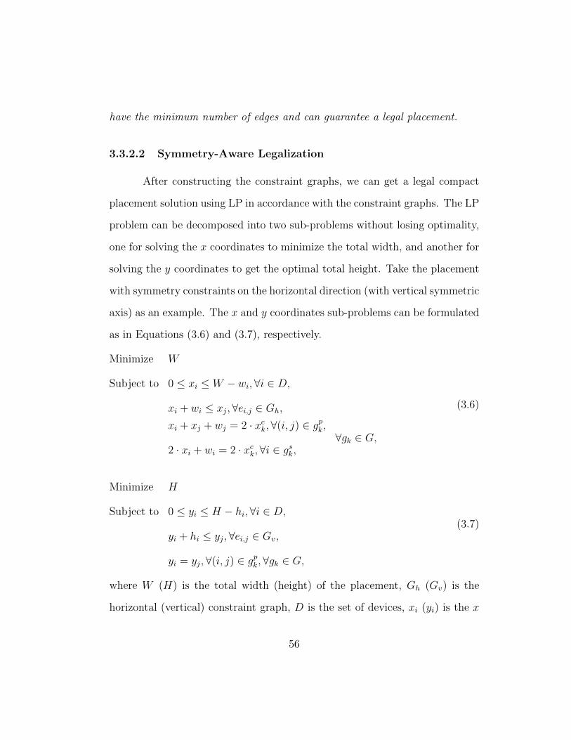
have the minimum number of edges and can guarantee a legal placement.
3.3.2.2 Symmetry-Aware Legalization
After constructing the constraint graphs, we can get a legal compact
placement solution using LP in accordance with the constraint graphs. The LP
problem can be decomposed into two sub-problems without losing optimality,
one for solving the x coordinates to minimize the total width, and another for
solving the y coordinates to get the optimal total height. Take the placement
with symmetry constraints on the horizontal direction (with vertical symmetric
axis) as an example. The x and y coordinates sub-problems can be formulated
as in Equations (3.6) and (3.7), respectively.
Minimize W
Subject to 0 ≤ xi ≤ W − wi,∀i ∈ D,
xi + wi ≤ xj,∀ei,j ∈ Gh,
xi + xj + wj = 2 · xck,∀(i, j) ∈ gpk,
2 · xi + wi = 2 · xck,∀i ∈ gsk,∀gk ∈ G,
(3.6)
Minimize H
Subject to 0 ≤ yi ≤ H − hi,∀i ∈ D,
yi + hi ≤ yj, ∀ei,j ∈ Gv,
yi = yj,∀(i, j) ∈ gpk, ∀gk ∈ G,
(3.7)
where W (H) is the total width (height) of the placement, Gh (Gv) is the
horizontal (vertical) constraint graph, D is the set of devices, xi (yi) is the x
56
(y) coordinate of the lower-left corner of device i, wi (hi) is the width (height)
of device i, G is the set of symmetric groups, gpk and gsk are the set of symmetric
pairs and the set of self-symmetric devices in a symmetric group gk respectively,
and xck is the coordinate of the symmetric axis of the group gk. There are
two sets of constraints which are topology order (non-overlap) and symmetry
constraints. The topology order constraints are from the constraint graphs
obtained by the previous section, while the symmetry constraints are directly
from the design specification. The y coordinates sub-problem differs from the
x coordinates sub-problem in that the x coordinates of a symmetric pair need
to be symmetric with respect to an axis (i.e., xi + xj + wj = 2 · xck), while
their y coordinates need to be the same (i.e., yi = yj). The LP problems for
the symmetry constraints on the vertical direction (with horizontal symmetric
axis) can be formulated in a similar way.
3.3.3 Detailed Placement
After legalization, we can get a legal compact placement solution. In
the detailed placement stage, we will use LP to further optimize the wire-
length for the given legal placement. The formulations are similar to Equa-
tions (3.6) and (3.7) in the legalization step, except that the placement bound-
aries are fixed to the optimal total width and height obtained from legalization
to ensure that the placement remains compact, and the optimization objective
becomes minimizing wirelength, which is shown in Equation (3.8), where W ∗
57

and H∗ are the optimal total width and height obtained from legalization.
Minimize Wirelength
Subject to 0 ≤ xi ≤ W ∗ − wi,∀i ∈ D,
xi + wi ≤ xj, ∀ei,j ∈ Gh,
0 ≤ yi ≤ H∗ − hi, ∀i ∈ D,
yi + hi ≤ yj,∀ei,j ∈ Gv,
xi + xj + wj = 2 · xck, ∀(i, j) ∈ gpk,
2 · xi + wi = 2 · xck,∀i ∈ gsk,
yi = yj,∀(i, j) ∈ gpk,
∀gk ∈ G,
(3.8)
3.4 Experimental Results
All algorithms are implemented in C++ and all experiments are per-
formed on a Linux machine with 3.4GHz Intel(R) core and 32GB memory.
WNLIB [67] is used as the unconstrained non-linear optimization solver for the
global placement. All benchmark circuits used are from experienced analog
circuit designers, reflecting the real analog design complexities. Benchmark
1 is an operational amplifier (opamp), which can be widely used to imple-
ment gain, filtering, buffering, and voltage regulation. Benchmark 2 is a gm-C
integrator, which can be found in low-power continuous-time filters. Bench-
mark 3 is a continuous-time delta-sigma modulator (CTDSM). CTDSMs are
oversampling ADCs that leverage noise-shaping. As specified by the circuit
designer, all capacitors in the circuit benchmarks are allowed to overlap the
58

transistors and resistors without degrading the circuit performance. The de-
vices in benchmark 1 and 2 include Type I and Type II devices. Benchmark
3 contains not only Type I and Type II devices, but also Type III devices.
The benchmark circuit information is summarized in Table 3.3. In the rest of
this section, Section 3.4.1 compares the placement results with and without
device layer-awareness, Section 3.4.2 shows the routability of the placement,
and Section 3.4.3 demonstrates the effectiveness of the analytical framework
by comparing with the baseline algorithm.
Table 3.3: Benchmark circuits information.
Index Design #Devices #Type I #Type II #Type III #Nets
1 opamp 46 42 4 0 29
2gm-C
integrator15 13 2 0 9
3 CTDSM 21 6 2 13 27
3.4.1 Effects of Device Layer-Awareness
Table 3.4 compares the placement results with and without device layer-
awareness in our analytical analog placement framework, where “NLP” means
the placement results without device layer-awareness, and “Device layer-aware
NLP” means the placement results with device layer-awareness. We can see
that area and HPWL benefits are consistently achieved (on average 9% and
23% reduction, respectively) when we co-optimize the devices occupying dif-
ferent layers during placement. The run-time is comparable with and without
device layer-awareness.
59

Table 3.4: Results of our analytical analog placement framework (NLP).
Metric DesignNLP Device layer-aware NLP
area(µm2)
HPWL(µm)
run-time (s)
area(µm2)
HPWL(µm)
run-time (s)
Valueopamp 2973 753 17.1 2370 498 10.9gm-C
integrator182 73 1.2 175 60 1.2
CTDSM 57455 3129 6.5 56060 2580 6.5
Ratioopamp 1 1 1 0.80 0.66 0.64gm-C
integrator1 1 1 0.96 0.83 1.00
CTDSM 1 1 1 0.98 0.82 1.00
average 1 1 1 0.91 0.77 0.88
3.4.2 Routability Verification
3.4.2.1 Analog Global Routing
Since the Type II and Type III devices occupy metal and via layers,
they will create routing blockages and lead to fewer available routing resources.
From this perspective, routing congestion and the resulting wirelength might
be a concern. To validate the routability of the proposed device layer-aware
layout scheme, a maze routing based analog global router is developed.
Maze routing is a classic and efficient routing strategy widely used in
routers [6, 8, 56]. Although it is time consuming compared to other routing
methods, the result quality is good due to its optimality for two-pin net. Since
there exists a limited number of nets in a constrained area for typical analog
circuits, it is preferable to utilize maze routing for designing wire connections.
To save the search space, we introduce a detour ratio defining how much
60

detour is allowed. If a legal solution cannot be acquired within the bounding
regions defined by the ratio, it will be relaxed to a larger value to cover more
routing resources. By constraining the region to be explored, the run-time
of our global routing can be controlled efficiently. Meanwhile, to handle the
specific characteristics brought by analog circuits, we extend the traditional
maze routing by introducing the adjustments as follows.
It is known that the symmetric nets in analog circuits should conform
to the stringent topological symmetry constraints. Thus we prefer to route
the symmetric nets with higher priorities than the others in our sequential
global routing algorithm. Also, as the topologies for two symmetric nets have
to satisfy the symmetric constraints, we will treat the symmetric nets as one
routing object, similar to [53,54]. Hence, we consider the blockages confronted
by both nets to generate the feasible route.
3.4.2.2 Congestion Analysis
In our global routing settings, the grid size and routing capacity inside
each grid are determined by the metal pitch defined in Process Design Kit
(PDK). The number of metal layers used for routing is set to 6, according to
the common practice of manual analog layout. This is because our benchmark
circuits usually serve as buildings blocks for a larger system, and the higher
metal layers can be used for interconnection across different building blocks.
The Type II devices in our benchmarks occupy metal layers 3 to 6, while
the Type III devices occupy the substrate, polysilicon, and metal layers 1 to
61

Table 3.5: Global routing (GR) results for the proposed analytical placementframework (NLP).
wirelength (µm)NLP + GR
Device layer-awareNLP + GR
value ratio value ratio
opamp 839 1 617 0.74gm-C integrator 89 1 79 0.89
CTDSM 3591 1 3034 0.84
average 1 0.82
Table 3.6: Results of MILP-based placement with quality matching (MILP-Q)our framework without device layer-awareness (NLP).
DesignMILP-Q
area (µm2) HPWL (µm) run-time (s)value ratio value ratio value ratio
opamp 3295 1.11 714 0.95 607.2 35.57gm-C integrator 187 1.03 69 0.95 20.7 17.21
CTDSM 57960 1.01 3611 1.15 20.5 3.16
average 1.05 1.02 18.65
3. The grids occupied by these devices will be marked as routing blockages
on corresponding layers. After running global routing, the results are listed
in Table 3.5, which verify the routability of our device layer-aware analog
placement solutions. An average of 18% wirelength improvement is observed,
compared with the global routing results on the non-overlapping placement
solutions. The run-time of the global routing is very fast (i.e., less than 0.5
seconds), and it is not listed in the table.
62

Table 3.7: Results of MILP-based placement with run-time matching (MILP-R) our framework without device layer-awareness (NLP).
DesignMILP-R
area (µm2) HPWL (µm) run-time (s)value ratio value ratio value ratio
opamp 4181 1.41 927 1.23 20.2 1.19gm-C integrator 184 1.01 77 1.06 5.7 4.73
CTDSM 64472 1.12 3443 1.10 10.5 1.62
average 1.18 1.13 2.51
3.4.3 Effectiveness of the Analytical Framework
We further compare our analytical analog placement framework with
the Mixed-Integer Linear Programming (MILP) based analog placement en-
gine in [99]. Since none of the previous work considered the overlaps be-
tween devices on mutually exclusive manufacturing layers during the place-
ment stage, the comparisons are done in the setting without device layer-
awareness. Table 3.6 and Table 3.7 show the comparisons between the results
of our analytical framework (NLP) and the baseline algorithm (MILP). In the
tables, all the metrics are normalized with respect to the results set NLP. The
set of results MILP-Q is generated by running the MILP-based placement un-
til it reaches comparable quality as the results set NLP. Another set of results
MILP-R is generated by specifying the same (or similar) run-time as the re-
sults set NLP, or when the MILP-based algorithm begins to find a solution.
Comparing the results sets MILP-Q and NLP, our analytical framework gen-
erates comparable (or better) results with the run-time speedup of above 18×.
On the other hand, comparing the results sets MILP-R and NLP, we can see
63

that our analytical framework is able to achieve better total placement area
and HPWL given the similar run-time (18% area reduction and 13% HPWL
improvement on average). Therefore, we can conclude that even when we dis-
able the capability of device layers-awareness, our results are still better than
the baseline MILP-based algorithm. Note that for the circuits with a small
number of placement devices (e.g., gm-C integrator and CTDSM circuits), the
MILP-based algorithm is effective in achieving good quality in reasonable run-
time. However, for medium or large size circuits (e.g., opamp), our analytical
framework is much more efficient than [99] to achieve good quality in a short
run-time, demonstrating the scalability of our algorithm.
3.5 Summary
In this chapter, we have presented a device layer-aware analog place-
ment. Different from the prior work where non-overlapping constraints were
imposed on every pair of devices, we strategically overlap the devices which
reside on mutually exclusive manufacturing layers and are insensitive to cou-
pling, so that the total area and wirelength can be effectively reduced without
degrading the circuit performance. We propose an analytical framework to
tackle the device layer-aware analog placement problem. We also develop an
analog global router to verify the routability of the device layer-aware analog
placement solutions. Experimental results show that the proposed techniques
can improve the total area and HPWL by 9% and 23%, respectively, and can
also achieve an average of 18% reduction on the wirelength after global routing.
64

Chapter 4
Analog Placement Constraint Extraction and
Exploration with the Application to Layout
Retargeting
The previous two chapters have addressed the practical issues in the di-
rection of optimization-based analog layout automation. This chapter switches
to the direction of the template-based approach and proposes a new layout re-
targeting framework which is flexible in exploring various layout topologies.
4.1 Introduction
Analog/mixed-signal (AMS) integrated circuits (ICs) are used widely
and heavily in many emerging applications, including consumer electronics,
automotive, and Internet of Things (IoT). The increasing demand of these ap-
plications calls for a shorter design cycle and time-to-market of AMS ICs. How-
ever, most of the design efforts in AMS ICs are still handled manually, which
is time-consuming and error-prone, especially as the design rules are becom-
This chapter is based on the following publication: Biying Xu, Bulent Basaran, MingSu, and David Z. Pan, “Analog Placement Constraint Extraction and Exploration with theApplication to Layout Retargeting, ” ACM International Symposium on Physical Design(ISPD), 2018. I am the main contributor in charge of problem formulation, algorithmdevelopment and experimental validations.
65

ing more and more complicated in nanometer-scale IC era, and as the circuit
performance requirements are becoming more and more stringent. Despite the
progress in the AMS IC layout design automation field [39, 50, 59, 72, 83, 99],
the automatic layout tools have not been widely used among AMS IC lay-
out designers. The AMS IC design automation level is far from meeting the
need for fast layout-circuit performance iterations for the rapid growth of the
market.
Given the vast amount of previous high-quality analog layouts, it is
desirable to explore the layout design constraints from them. The extracted
layout constraints can be applied in layout technology migration [27, 31], re-
targeting to updated design specifications (performance retargeting) [57,105],
and knowledge-based layout synthesis [94], etc., to preserve experts’ knowledge
across designs, shorten design cycle and reduce design efforts. Layout technol-
ogy migration and performance retargeting are called layout retargeting.
In [27], a layout technology migration tool Migration Assistant Shape
Handler (MASH) was proposed, which addressed the geometry scaling be-
tween technologies and corrected design rule violations with minimum layout
perturbations. Nevertheless, it did not consider the layout design constraints
in AMS ICs, including symmetry (symmetry-island [50]), regularity, matching,
etc. Then, in [31], N. Jangkrajarng et al. presented an intellectual property
reuse-based analog IC layout automation tool, IPRAIL, that could automat-
ically retarget existing analog layouts for new process technologies and new
design specifications. Previous works [105] and [57] further improved the ana-
66

log layout retargeting algorithm by considering layout parasitics and circuit
performance degradation. The above-mentioned prior works [31, 57, 105] ex-
tracted the topological template from the existing layout so that the target
layout had the same layout topology, and they automatically detected symme-
try in the existing layouts and carried the symmetry constraints to the target
layout, as well. More recently, P.-H. Wu et al. proposed a knowledge-based
analog physical synthesis methodology to generate new layouts by integrat-
ing existing design expertise [94]. It extracted common sub-circuits between
previous designs and the target design and reused quality-approved layout
topologies.
However, the previous works on analog layout retargeting had the fol-
lowing limitations. Firstly, although symmetry constraints were extracted
from the existing layouts and preserved in the target layout, regularity con-
straints were not considered, including topological rows, columns, arrays, and
repetitive structures, which are common in AMS ICs. Regular structures in
AMS IC layouts not only improve routability, but also minimize the number
of vias and bends of wires that are critical, and reduce the layout parasitics-
induced circuit performance degradation [64, 65]. Thus, it is beneficial to
take regularity constraints into account. Secondly, previous works extracted
a topological template from the existing layout to preserve the entire layout
topology. Nevertheless, it may introduce unnecessary extra topological con-
straints and limit the solution space. In fact, due to new process technologies
or updated design specifications, the device sizes may not scale proportionally
67

during layout retargeting, and it may be more desirable to adopt a different
layout topology. To address these limitations, in this work, we extract and
explore the regularity and symmetry (symmetry-island) constraints from pre-
vious quality-approved layouts. The extracted constraints are applied to a
novel analog layout retargeting framework to preserve the design expertise.
An efficient sweep line-based algorithm is developed to extract the regularity
constraints from a given analog placement. Our main contributions include:
• We extract and explore symmetry and regularity constraints in previous
high-quality layouts.
• For the first time, an efficient sweep line-based algorithm is developed
to extract all the regularity constraints in an analog placement.
• We propose a novel analog layout retargeting framework based on the
extracted constraints, which reduces the placement area compared with
the conventional approach while preserving the design expertise.
• Experimental results show the effectiveness and efficiency of the proposed
techniques.
The rest of this chapter is organized as follows. Section 4.2 shows the
overall flow of the proposed analog layout retargeting framework. Section
4.3 describes the algorithms to extract analog placement constraints. Section
4.4 describes the regularity and symmetry constraint-aware analog placement
68

algorithm used in the proposed layout retargeting framework. Section 4.5
shows the experimental results. Finally, Section 4.6 summarizes the chapter.
4.2 Overall Flow
Conventionally, most of the prior works on analog layout retargeting
extract symmetry (symmetry-island) constraints and a topological template
of the existing layout, followed by a constraint-aware layout compactor to pre-
serve the extracted constraints and the entire layout topology. The conven-
tional analog layout retargeting framework is shown in Figure 4.1a, where only
symmetry constraints were considered. The layout compactor only generates
the layout with the same topology as the existing one.
The proposed analog layout retargeting flow based on placement con-
straint extraction is shown in Figure 4.1b. First, the constraint extraction en-
gine explores various analog placement constraints in the existing placement,
including regularity and symmetry constraints. Different from the conven-
tional framework that only detects symmetry constraints, we are the first to
propose an efficient sweep line-based algorithm to extract the regularity con-
straints, which will be described in Section 4.3. Then, given the extracted
constraints and the updated device sizes due to new process technologies or
new design specifications, a constraint-aware analog placement is performed
such that the design expertise is preserved. Adopting constraint-aware analog
placement engine instead of analog layout compactor with fixed layout topol-
ogy provides the potential to explore various different placement topologies,
69

which may result in the placement quality improvement. The constraint-aware
analog placement algorithm will be described in Section 4.4.
Symmetry Constraint Extraction
Constraint-Aware Analog Layout Compactor
Layout Topology Extraction
UpdatedDevice sizes
Layout Template Extractor
Analog Layout Constraints &
Topological Template
ExistingLayout
TargetLayout
(a)
Regularity Constraint Extraction
Analog Placement Constraints
Constraint-Aware Analog Placement
Symmetry Constraint Extraction
Existing Placement
UpdatedDevice sizes
TargetPlacement
Layout Constraint Extractor
(b)
Figure 4.1: (a) The conventional analog layout retargeting framework. (b)The overall flow of the proposed analog layout retargeting framework.
4.3 Layout Constraint Extraction
4.3.1 Regularity Constraint Extraction
AMS IC placements often contain regular structures which are also
called regularity constraints [65]. A regular structure is composed of a group
of devices forming a slicing structure whose rectangular bounding box in the
70

10
9
12
4
7
1 32
65
811
column
row
array
Figure 4.2: An example of AMS circuit placement. Orange: row constraint;Blue: column constraint; Red: array.
placement does not cut any device bounding box. Figure 4.2 shows an example
of an analog placement with regularity constraints. Each rectangle represents
the bounding box of a placement device (e.g. a transistor). The orange bound-
ing boxes indicate row constraints. For example, devices 10, 11 form a row.
The blue bounding boxes indicate column constraints. For example, devices
1, 2, 3, 4, 5, 6 and devices 7, 8 are four rows in a column. The array con-
straints are indicated by red bounding boxes. For instance, devices 1, 2, 3, 4,
5, 6 form a 2-row-by-3-column array. If all the devices in row/column/array
A are inside another bigger row/column/array B, and the set of slicing lines
of A is a subset of that of B, we say that row/column/array A is dominated
by row/column/array B. Otherwise, A is not dominated by B. As an exam-
ple, the row consisting of devices 1, 2 is dominated by the row consisting of
devices 1, 2, 3, and the row consisting of devices 1, 2, 3 is dominated by
the array consisting of devices 1, 2, 3, 4, 5, 6. The regularity constraint ex-
traction problem is to find all the regular structures which are not dominated
by any other regular structure in an analog placement.
71

4.3.1.1 Lookup Table Construction
We first turn the placement into a grid-based representation. A device
bounding box can be represented by the x (horizontal) coordinates of its left
and right edges, and the y (vertical) coordinates of its bottom and top edges.
The entire placement can be divided by the Hanan grid of all device bounding
boxes, which is built based on the horizontal and vertical sweep lines. We
construct the sets of horizontal and vertical sweep lines as follows. For each
device bounding box in the placement, a vertical sweep line is added for the
x coordinate of its left edge, and another vertical sweep line is added for the
x coordinate of its right edge. For the vertical sweep lines with the same x
coordinate, only one is added to the set. Therefore, the total number of ver-
tical sweep lines is less than two times of the number of placement devices.
Similarly, two horizontal sweep lines are added for the y coordinates of the
bottom and top edges of a device, respectively. Figure 4.3a shows the place-
ment of Figure 4.2 with the Hanan grid. In Figure 4.3, “H/V” stands for
“horizontal/vertical”, respectively.
Then, several Boolean lookup tables (LUTs) are constructed which
will be used by the sweep line-based algorithm as described later. For the
subscripts of the LUTs, “d” stands for “device”, “l” is for “sweep line”, and
“r” is for “region”. For example, the LUT Vdr tells us the relationship between
a device and a vertical region. The LUTs Vdr and Hdr shown in Figure 4.3b
indicate which region each device bounding box in Figure 4.3a lies in. A
region is defined as the range between adjacent sweep lines. For example, a
72

10
9
12
4
7
1 32
65
811
0 1 2 3 4 5 6 7 8 9
0
1
2345
67
8
V sweep linesH sweep lines
(a)
0 1 2 3 4 5 6 7 8
0 1 2 3 4 5 6 7
12
12
0 0 0 0 1 0 0 0 00 0 0 0 0 0 1 0 0
0 0 1 1 1 1 1 1 1
12
12
0 0 0 0 0 0 0 10 0 0 0 0 0 0 1
1 0 0 0 0 0 0 0
V
H
… …
… …
V regions
H regions
devices
devices
dr
dr
(b)
0 1 2 3 4 5 6 7 8 9
0 1 2 3 4 5 6 7 8
12
12
0 0 0 0 0 0 0 0 0 00 0 0 0 0 0 0 0 0 0
0 0 0 1 1 1 1 1 1 0
1
9
12
0 0 0 0 0 0 0 0 0
0 0 0 0 1 1 1 1 0
0 0 0 0 0 0 0 0 0
V
H
…
…
… …
…
…
V sweep lines
H sweep lines
devices
devices
dl
dl
(c)
0 1 2 3 4 5 6 7 8
0 1 2 3 4 5 6 7
01
8
0 0 0 0 0 0 0 0 01 1 0 0 0 0 0 0 0
1 1 1 0 0 0 0 0 00 0 0 0 0 0 0 0 0
01
9
0 0 0 0 0 0 0 00 0 0 1 1 1 1 1
0 0 0 0 0 0 0 0
H
V
… …
… …
V regionsH sweep lines
V sweep lines
H regions
7
lr
lr
(d)
Figure 4.3: (a) The example analog placement in Figure 4.2 with the grids.(b) LUT Vdr and Hdr. (c) Vdl and Hdl. (d) Vlr and Hlr.
73

vertical region i is between vertical sweep lines i and i + 1. The number of
vertical regions is one less than the number of vertical sweep lines. Each row
in Vdr indicates which vertical region a device bounding box occupies. As an
example, device 12 lies between vertical sweep lines 2 and 9, i.e. it occupies
vertical regions 2, 3, · · · , 8. Hence, there are 1’s at indices 2, 3, · · · , 8
and 0’s elsewhere on the row corresponding to device 12 in Vdr. Similarly, the
horizontal region is defined and Hdr is constructed.
The LUTs Vdl and Hdl shown in Figure 4.3c indicate the vertical or
horizontal sweep lines a device bounding box strictly intersects. We say that
an HR/VR/ HSL/VSL (see Table 4.1) strictly intersect with a device when
there is at least some portion of the HR/VR/HSL/VSL that is strictly inside
the device bounding box, not including the borders of the bounding box. For
instance, device 1 does not strictly intersect any vertical sweep line nor hori-
zontal sweep line, so the rows corresponding to device 1 have all 0’s in Vdl and
Hdl. Device 9 strictly intersects horizontal sweep lines 4, 5, 6, 7, so there
are 1’s at indices 4, 5, 6, 7 and 0’s elsewhere on the row corresponding to
device 9 in Hdl. The first and the last columns in Vdl and Hdl consist of all
0’s, since the first and the last sweep lines will not strictly intersect with any
device. Once we have constructed Vdr and Hdr, Vdl and Hdl can be computed
by bitwise operations efficiently:
Vdl[d] = Vdr[d]&(Vdr[d] 1), Hdl[d] = Hdr[d]&(Hdr[d] 1)
where “d” is the device index, “&” stands for the bitwise and operation, and
74

“” is the bitwise left shift operation.
The LUTs Vlr and Hlr shown in Figure 4.3d indicate whether a sweep
line strictly intersects any device bounding box in a region. Each row in the
LUT corresponds to a sweep line, and each column in the LUT corresponds to
a region. For example, the vertical sweep line 1 strictly intersects device 9 in
horizontal regions 3 to 7. Therefore, in LUT Vlr, row 1 has 1’s in columns 3,
4, · · · , 7. Note that the first and the last rows in Vlr and Hlr are all 0’s, since
the first and the last sweep lines will not strictly intersect with any device in
any region. LUTs Vlr and Hlr can be computed from Vdr, Hdr, Vdl and Hdl as
follows:
Vlr[i][j] =∨d
(Vdl[d][i] ∧Hdr[d][j]), Hlr[i][j] =∨d
(Hdl[d][i] ∧ Vdr[d][j])
where “d” is the device index, “∧” is the logical conjunction operator, and
“∨
” is the logical disjunction operator. Overall, the time complexity for LUT
construction is O(n), where n is the number of placement devices.
4.3.1.2 Sweep Line-Based Algorithm
A sweep line-based algorithm is proposed to extract all the regularity
constraints in an analog placement. The notations used are listed in Table 4.1.
The overall algorithm is described in Algorithm 4. The algorithm is based on
the observation that if there is a slicing line segment between point A and point
B for the placement (i.e., the line segment AB does not strictly intersect any
device bounding box), then for every point C on AB, AC and CB must also
75

Table 4.1: Notations for layout constraint extraction.
HSL Horizontal sweep line.
VSL Vertical sweep line.
HR Horizontal region.
VR Vertical region.
VRj The j-th VR.
Rfin All regular structure results.
Rpar Intermediate/partial regular structures.
rh, rvConsecutive HRs and VRs in the intermediate/final
regular structure.
lh, lvSlicing HSLs and VSLs in the intermediate/final regular
structure.(rh, lh, rv, lv) Represents an intermediate or final regular structure.
fv Indicates if the consecutive HRs are slicing at a VSL.
fh Indicates if a set of HSLs are slicing at a VR.
Q A set of consecutive HRs that are slicing at a VSL.
be slicing for the placement. The terminology is defined as follows:
Definition 2 (Slicing Region). If an HR/VR does not strictly intersect with
any device bounding box at a VSL/HSL, it is a slicing HR/VR at that
VSL/HSL.
Definition 3 (Sweep Line within a Region). An HSL/VSL is within a HR
/VR (or a region covers a sweep line) when the coordinate of the HSL/VSL is
within the region or at the region endpoints.
Figure 4.4, Figure 4.5, Figure 4.6 and Figure 4.7 show the intermediate
steps after Algorithm 4 proceeds to VSLs 1, 2, 3 and 4, respectively, when the
algorithm is applied to the analog placement example in Figure 4.2.
76
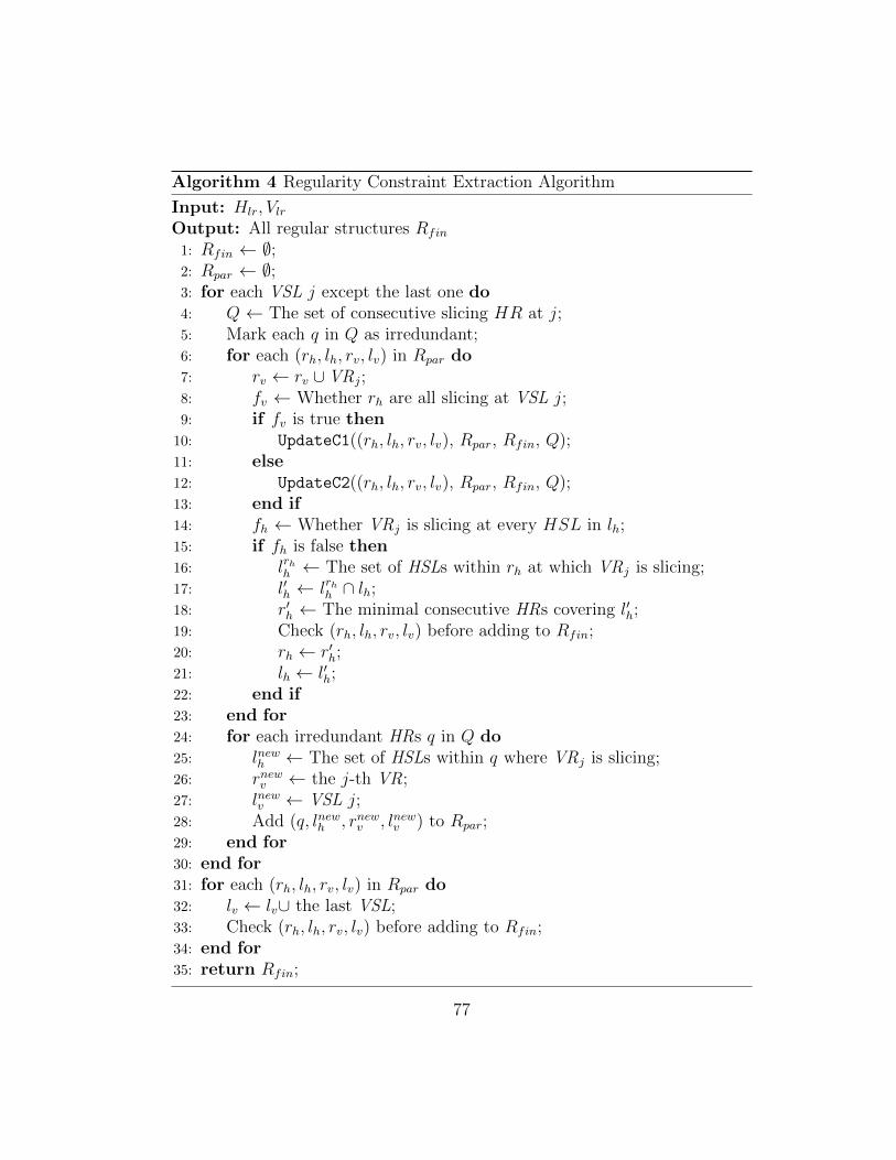
Algorithm 4 Regularity Constraint Extraction Algorithm
Input: Hlr, VlrOutput: All regular structures Rfin
1: Rfin ← ∅;2: Rpar ← ∅;3: for each VSL j except the last one do4: Q ← The set of consecutive slicing HR at j;5: Mark each q in Q as irredundant;6: for each (rh, lh, rv, lv) in Rpar do7: rv ← rv ∪ VRj;8: fv ← Whether rh are all slicing at VSL j;9: if fv is true then
10: UpdateC1((rh, lh, rv, lv), Rpar, Rfin, Q);11: else12: UpdateC2((rh, lh, rv, lv), Rpar, Rfin, Q);13: end if14: fh ← Whether VRj is slicing at every HSL in lh;15: if fh is false then16: lrhh ← The set of HSLs within rh at which VRj is slicing;17: l′h ← lrhh ∩ lh;18: r′h ← The minimal consecutive HRs covering l′h;19: Check (rh, lh, rv, lv) before adding to Rfin;20: rh ← r′h;21: lh ← l′h;22: end if23: end for24: for each irredundant HRs q in Q do25: lnewh ← The set of HSLs within q where VRj is slicing;26: rnewv ← the j-th VR;27: lnewv ← VSL j;28: Add (q, lnewh , rnewv , lnewv ) to Rpar;29: end for30: end for31: for each (rh, lh, rv, lv) in Rpar do32: lv ← lv∪ the last VSL;33: Check (rh, lh, rv, lv) before adding to Rfin;34: end for35: return Rfin;
77
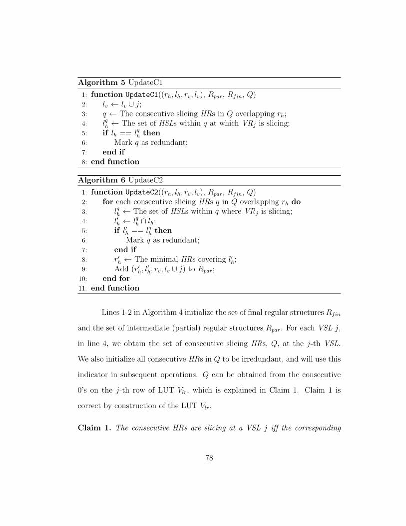
Algorithm 5 UpdateC1
1: function UpdateC1((rh, lh, rv, lv), Rpar, Rfin, Q)2: lv ← lv ∪ j;3: q ← The consecutive slicing HRs in Q overlapping rh;4: lqh ← The set of HSLs within q at which VRj is slicing;5: if lh == lqh then6: Mark q as redundant;7: end if8: end function
Algorithm 6 UpdateC2
1: function UpdateC2((rh, lh, rv, lv), Rpar, Rfin, Q)2: for each consecutive slicing HRs q in Q overlapping rh do3: lqh ← The set of HSLs within q where VRj is slicing;4: l′h ← lqh ∩ lh;5: if l′h == lqh then6: Mark q as redundant;7: end if8: r′h ← The minimal HRs covering l′h;9: Add (r′h, l
′h, rv, lv ∪ j) to Rpar;
10: end for11: end function
Lines 1-2 in Algorithm 4 initialize the set of final regular structures Rfin
and the set of intermediate (partial) regular structures Rpar. For each VSL j,
in line 4, we obtain the set of consecutive slicing HRs, Q, at the j-th VSL.
We also initialize all consecutive HRs in Q to be irredundant, and will use this
indicator in subsequent operations. Q can be obtained from the consecutive
0’s on the j-th row of LUT Vlr, which is explained in Claim 1. Claim 1 is
correct by construction of the LUT Vlr.
Claim 1. The consecutive HRs are slicing at a VSL j iff the corresponding
78

indices of the consecutive HRs have consecutive 0’s on the row Vlr[j] in Vlr.
Each intermediate or final regular structure can be represented by its
(rh, lh, rv, lv) (see Table 4.1). For each intermediate regular structure in Rpar,
rv is updated to contain the j-th VR (line 7 of Algorithm 4). We define two
indicator variables fv and fh, as shown in lines 11 and 12 and in Table 4.1.
fv can be obtained in a way similar to the way of obtaining Q. fv
indicates whether all the consecutive HRs in rh are slicing at VSL j. If it is
true, one and only one q in Q will overlap with rh, and Algorithm 5 will be
executed. In Algorithm 5, we first add j to the set of VSLs in the intermediate
result. Let q be the consecutive slicing HRs at j that overlap with rh, and
let lqh be the set of HSLs within q at which the j-th VR is slicing. If lqh is
the same as lh in the intermediate result under consideration, then q will be
marked as redundant, and no new intermediate regular structure needs to be
created for q, since it is contained in the existing intermediate result. This can
be illustrated by Figure 4.5. Before processing VSL 2, Rpar[1] (in green) has
rh = 0, 1, 2 and lv = 0, 1. The set of consecutive slicing HRs Q at VSL
2 only has one element q = 0, 1, 2. Therefore, fv is true for Rpar[1] at VSL
2, and VSL 2 is added to lv which makes lv 0, 1, 2. Since lqh = 0, 1, 2, 3
is not the same as lh = 0, 3, q is not marked as redundant when processing
Rpar[1] at VSL 2.
Otherwise, if fv is false, there may be zero or more HRs inQ overlapping
with rh, and Algorithm 6 will be executed. In Algorithm 6, for each consecutive
79

10
9
12
4
7
1 32
65
811
0 1
0
1
2345
67
8R [0]:rh = [0 to 7]lh = 0, 3, 8rv = [0 to 1]lv = 0R [1]:rh = [0 to 2]lh = 0, 3rv = [0 to 1]lv = 0, 1
2par
par
Figure 4.4: Applying Algorithm 4 to the placement in Figure 4.2 after pro-cessing VSLs 0 and 1.
slicing HRs q overlapping with rh, lqh is obtained as in the case where fv is true.
Then l′h, which is the intersection between lqh and lh, is calculated and compared
with lqh. If they are the same, then no new intermediate result for q needs to be
added to Rpar, and q is marked as redundant. After that, we find the minimal
HRs r′h covering l′h and add that intermediate result with VSL j to the set
Rpar. This process can be illustrated by Figure 4.4. Before processing VSL
1, Rpar[0] (in red) has rh = 1, 2, · · · , 7, but Q only consists of one element
which is q = 0, 1, 2. Hence, fv is false for Rpar[0]. lqh = 0, 3, and l′h is
the same as lqh. Therefore, q is marked as redundant and no new intermediate
result needs to be created for it. We find the minimal HRs r′h = 0, 1, 2, and
create a new intermediate result with (r′h, l′h, rv, lv ∪ j) (see Rpar[1] in green in
Figure 4.4). Lines 9 to 13 in Algorithm 4 call the two functions “UpdateC1”
(Algorithm 5) and “UpdateC2” (Algorithm 6) depending on fv.
fh can be obtained from the j-th column of LUT Hlr (see Claim 2, and
line 14 of Algorithm 4). Similar to Claim 1, Claim 2 also holds by construction
80

10
9
12
4
7
1 32
65
811
0 1
0
1
2345
67
8R [0]:rh = [0 to 7]lh = 0, 3, 8rv = [0 to 2]lv = 0R [1]:rh = [0 to 2]lh = 0, 3rv = [0 to 2]lv = 0, 1, 2
2 3 R [2]:rh = [0 to 2]lh = 0, 1, 2, 3rv = [2 to 2]lv = 2
par
par
par
Figure 4.5: Applying Algorithm 4 to the placement in Figure 4.2 after pro-cessing VSL 2.
of Hlr.
Claim 2. VR j is slicing at an HSL i iff Hlr[i][j] is 0.
If fh is true, it means the slicing HSLs in lh continues to be slicing at
the j-th VR. For instance, In Figure 4.4, before processing VSL 1, the rv of
Rpar[0] (in red) is 0 (only VR 0 is in rv). Since all the three HSLs in lh = 0,
3, 8 are slicing at VR 1, fh is true and VR 1 is added to rv which becomes
0, 1 after processing VSL 1 (see Figure 4.4).
Otherwise, if fh is false, it means at least one of the HSLs in lh is no
longer slicing at the j-th VR, and we will add the previous intermediate result
to the final result after trimming and checking whether the resulting regular
structure is valid (line 19 in Algorithm 4). That is, rh and rv will be trimmed
such that they are the minimal regions covering lh and lv (see Definition 3). We
also check to ensure that each of the rectangular regions formed by lh and lv
contains at least one device. This can be done by bitwise operations on Vdr and
Hdr. We further prune the final result such that the regular structure contains
81

more than 2 HSLs or more than 2 VSLs to form a valid regular structure.
Finally, the resulting regular structure will be compared against the existing
ones in Rfin to ensure that each regular structure is not dominated by any
other regular structure. After that, the existing intermediate result is updated
to contain only the continuing slicing VR (lines 20 to 21 in Algorithm 4).
Figure 4.7 shows the case where fh is false. Before processing VSL 4, Rpar[1]
(in green) have two HSLs lh = 0, 3 (as in Figure 4.6). However, the VR 4 is
not slicing at HSL 3, resulting in fh being false. We trim the rv from 0, 1, 2, 3
to 0, 1 (since lv = 0, 1, 2), and make sure that each of the 2 columns in the
row contains at least one device (devices 10 and 11, respectively). Therefore,
Rfin[0] is added the final result (see Figure 4.7). Since there is only one
HSL remaining in the original intermediate result which will no longer form a
regular structure, it will be removed. Similarly, for Rpar[3] in Figure 4.6 (in
cyan), its lh changes from 1, 2, 3, 4, 5, 6, 7, 8 to 1, 4, 5, 6, 7, 8. It remains
in Rpar but becomes Rpar[2] in Figure 4.7 since the original intermediate result
Rpar[1] in Figure 4.6 (in green) is removed. The resulting candidate to add to
Rfin with lh = 1, 2, 3, 4, 5, 6, 7, 8 and lv = 3, 4 is not valid because it
contains no device. Thus it is not added to Rfin.
After iterating through all the intermediate regular structures in Rpar,
for each of the consecutive slicing HRs q in Q that remains irredundant (i.e.
that is not marked as redundant by the algorithm), a new intermediate regular
structure is added to Rpar, as can be seen in lines 24-29 in Algorithm 4. The
new intermediate result has q, the j-th VR, and the VSL j. Its HSLs can
82

10
9
12
4
7
1 32
65
811
0 1
0
1
2345
67
8R [0]:rh = [0 to 7]lh = 0, 3, 8rv = [0 to 3]lv = 0R [1]:rh = [0 to 2]lh = 0, 3rv = [0 to 3]lv = 0, 1, 2
2 3 4 R [2]:rh = [0 to 2]lh = 0, 1, 2, 3rv = [2 to 3]lv = 2R [3]:rh = [1 to 7]lh = 1, 2, 3, 4, 5, 6, 7, 8rv = [3 to 3]lv = 3
R [4]:rh = [1 to 2]lh = 1, 2, 3rv = [2 to 3]lv = 2, 3
par
par
par
par
par
Figure 4.6: Applying Algorithm 4 to the placement in Figure 4.2 after pro-cessing VSL 3.
10
9
12
4
7
1 32
65
811
0 1
0
1
2345
67
8R [0]:rh = [0 to 7]lh = 0, 8rv = [0 to 4]lv = 0
2 3 4 R [1]:rh = [0 to 1]lh = 0, 1, 2rv = [2 to 4]lv = 2R [2]:rh = [1 to 7]lh = 1, 24, 5, 6, 7, 8rv = [3 to 4]lv = 3, 4
5 R [0]:rh = [0 to 2]lh = 0, 3rv = [0 to 1]lv = 0, 1, 2
finpar par
par
Figure 4.7: Applying Algorithm 4 to the placement in Figure 4.2 after pro-cessing VSL 4.
be obtained from Hlr similarly to the way of getting fh. Figure 4.5 shows an
example of adding a new intermediate regular structure for the irredundant
consecutive slicing HRs in Q. The set of consecutive slicing HRs Q at VSL 2
only has one element q = 0, 1, 2. It turns out that q remains irredundant
after processing both Rpar[0] and Rpar[1]. Therefore, a new intermediate result
Rpar[2] (in purple) with rh = 0, 1, 2, lh = 0, 1, 2, 3, rv = 2 and lv =
2 is added to the set Rpar.
The above procedure is performed for all the VSLs except the last
83

one. Finally, in lines 31-34 in Algorithm 4, the last VSL is added to the lv
for all the intermediate results in Rpar, and the updated regular structures
(rh, lh, rv, lv) are checked and trimmed before they are added to the Rfin, as
already described above.
4.3.1.3 Algorithm Analysis
The proposed sweep line-based algorithm is, in essence, a smart enu-
meration algorithm with pruning, and is guaranteed to find all the regularity
constraints.
Claim 3. Algorithm 4 finds all regular structures that are not dominated by
any other regular structure in an analog placement.
Proof. We begin with the proof that the results found by Algorithm 4 are
slicing structures and are not dominated by any other regular structure. The
proof is by induction. For the first VSL, the entire VSL is slicing, and it must
be irredundant. Therefore, the first intermediate result in Rpar is obviously
slicing (lines 24-29 in Algorithm 4). Now assume that the intermediate results
in Rpar are slicing just before the algorithm proceeds to the j-th VSL. There
are two cases depending on fv (lines 9-13 in Algorithm 4). In Algorithm 5,
VSL j is slicing and is added to lv, thus the intermediate regular structure is
still slicing. In Algorithm 6, (r′h, l′h, rv, lv ∪ j) is a slicing structure, and after
it is added to Rpar, the slicing property of the intermediate regular structure
still holds. When l′h is assigned to lh (line 21 in Algorithm 4), the slicing
84

property is maintained. When (q, lnewh , rnewv , lnewv ) is added to Rpar (line 28 in
Algorithm 4), the slicing property is still maintained. As a result, we know
that after processing the j-th VSL, the intermediate results in Rpar are all
slicing. For the last VSL, the entire VSL is slicing, after adding it to the lv
of every intermediate regular structure, the results are still slicing. Note that
before adding to Rfin, the regular structure is compared against other regular
structures to ensure there is no dominance relationship. Therefore, the results
found by Algorithm 4 are slicing structures and are not dominated by any
other regular structure.
Next, we show that any regular structure that is not dominated by other
regular structures will be found by Algorithm 4. Let (r∗h, l∗h, r∗v, l∗v) be any of
these regular structures. Let j∗ be the first VSL in l∗v. VSL j∗ must be slicing
at some irredundant HRs q and r∗h ⊆ q, since otherwise the regular structure
must be in a larger regular structure, which contradicts with the condition
that there is no dominance relationship. Lines 24-29 in Algorithm 4 adds
the intermediate result (q, lnewh , rnewv , lnewv ) to Rpar, where r∗h ⊆ q, l∗h ⊆ lnewh ,
rnewv = VR j∗, lnewv = VSL j∗. Then, before processing the last VSL in l∗v,
for every HSL in lnewh but not in l∗h, there must be some VR where it is not
slicing, therefore, fh will be false and the HSL will be removed from lh of the
intermediate result. In contrast, all HSL in l∗h will remain in lh. As for the
VSLs, from j∗ until the last VSL in l∗v, if the VSL /∈ l∗v, fv must be false, it is
not added to the lv of the intermediate result. On the contrary, if the VSL ∈ l∗v,
there are two cases depending on fv. If fv is true, in Algorithm 5, the VSL is
85
added to lv of the intermediate result. Otherwise, if fv is false, in Algorithm 6,
there must be some q ∈ Q overlapping r∗h. r′h must contain r∗h, and l′h must
contain l∗h, hence the newly added intermediate result by line 8 in Algorithm 6
will continue to produce (r∗h, l∗h, r∗v, l∗v). Before processing the last VSL in l∗v,
the intermediate result contains exactly l∗h and all the VSLs in l∗v except the
last one. For the last VSL in l∗v, fv must be true and fh must be false. The
last VSL in l∗v is added to the lv of the intermediate regular structure which
makes it the same as l∗v, thus the regular structure (r∗h, l∗h, r∗v, l∗v) is added to
Rfin. Therefore, any regular structure that is not dominated by other regular
structures will be found by Algorithm 4.
Most of the operations in the proposed algorithm are bitwise operations
and efficient. Let n be the number of placement devices. The outer loop of
Algorithm 4 is executed O(n) times. In each iteration of the outer loop, the
number of intermediate regular structures is O(n3). Inside the inner loop,
with bitwise operations and parallelization, the run-time is O(1). Therefore,
the time complexity of the proposed algorithm is O(n4).
4.3.2 Symmetry Constraint Extraction
Device layout matching is crucial to enhance the robustness of matched
devices to process variations, thermal gradients, etc. [11] Symmetry constraints
are usually used to provided 1:1 matching of device pairs. We will extract
and preserve the mirror symmetry/symmetry-island constraints during layout
retargeting. The algorithm used to extract the constraints is developed based
86

M0_0 M1_1 M1_0M0_1
Figure 4.8: Example placement with a mirror symmetry constraint.
on [5, 31], and described as follows.
Figure 4.8 shows an example of a mirror symmetry constraint. Device
M0 is divided into two equal size elements, M0 0 and M0 1, respectively (in
grey). Similarly, device M1 is also split into M1 0 and M1 1 (in blue). Since
M0 0 is symmetric to M1 0, and M0 1 is symmetric to M1 1, with respect
to the same vertical axis, hence, M0 and M1 are in a mirror symmetry con-
straint. To extract mirror symmetry/symmetry-island placement constraints,
first, the devices are grouped by their types (e.g., NMOS, PMOS, resistor,
capacitor, etc.). Then, for the same type of devices, sub-groups are further
formed according to their physical dimensions, i.e., widths and heights. Within
the device sub-groups with the same type and dimension, we extract the mir-
ror symmetry placement constraints based on the center coordinates of the
devices.
4.4 Constraint-Aware Placement
After the regularity constraints and symmetry (symmetry-island) con-
straints are extracted from the existing layout, the next step is to perform
constraint-aware analog placement considering the extracted constraints and
updated device sizes. The extracted constraints are general and can be applied
87

to any constraint-aware analog placement engine that can handle regularity
constraints and symmetry (symmetry-island) constraints, e.g., [51, 65, 83, 99].
The analog placement engine used in our layout retargeting flow is based on
the Mixed-Integer Linear Programming (MILP) formulation, and the non-
overlapping constraints and symmetry-island constraints are formulated simi-
larly to [99].
As for the regularity constraints, we have the following conditions:
1) Conditions for devices inside the constraint: The devices inside the
regularity constraint are separated by slicing lines. The devices in the i-th row
and j-th column of the regular structure must lie inside the box formed by the
i-th and (i+ 1)-th horizontal slicing lines and the j-th and (j + 1)-th vertical
slicing lines.
Let Di,j,k be the set of devices in the i-th (i < ik) row and j-th (j < jk)
column in the regularity constraint k, where ik is the number of rows and jk is
the number of columns in the regular structure, respectively. Let xd be the x
coordinate and yd be the y coordinate of device d. For a regularity constraint
with ik rows and jk columns, there should be ik + 1 HSLs and jk + 1 VSLs
separating the rows and columns. We introduce ik + 1 auxiliary variables, i.e.,
yk,0r , yk,1r , . . . , yk,ik
r , to represent the y coordinates of the HSLs. Similarly, we
introduce jk + 1 auxiliary variables, i.e., xk,0r , xk,1r , . . . , xk,jk
r , to represent the x
coordinates of the VSLs. Assuming that the rows and HSLs are ordered from
bottom to top, and that the columns and VSLs are ordered from left to right,
the devices in Di,j,k must lie inside the box formed by xk,jr , xk,j+1r , yk,ir , and
88

yk,i+1r :
xd ≥ xk,jr , xd ≤ xk,j+1r , yd ≥ yk,ir , yd ≤ yk,i+1
r ,∀d ∈ Di,j,k
2) Conditions for devices outside of the constraint: The devices outside
of the regularity constraint must not overlap the bounding box formed by the
devices inside the regularity constraint.
For each d′ /∈ Di,j,k, we introduce a pair of auxiliary binary variables
skd′ and tkd′ to ensure the non-overlapping property. The following inequalities
must be satisfied:xd′ +MW (skd′ + tkd′) ≥ xk,j
k
r
xd′ + wd′ −MW (1 + skd′ − tkd′) ≤ xk,0r
yd′ +MH(1− skd′ + tkd′) ≥ yk,ik
r
yd′ + hd′ −MH(2− skd′ − tkd′) ≤ yk,0r
∀d′ /∈ Di,j,k
where MW and MH are sufficiently large constants (big-M method [84]), such
that no matter what binary values skd′ and tkd′ are, only 1 out of the 4 inequalities
takes effect, while other inequalities are left ineffective.
In the implementation, the orientations of the devices inside a regularity
constraint are preserved during retargeting. Also, our placement engine takes
the layout compaction result of the conventional layout retargeting approach
as a starting point so that our placement quality will not be worse than the
conventional approach.
89

Table 4.2: Benchmark AMS IC placements.
Placement #Devices#RowConst.
#ColumnConst.
#ArrayConst.
#Sym.Const.
1 45 3 9 3 142 50 5 14 0 183 200 20 56 1 72
4.5 Experimental Results
All algorithms are implemented in C++ and all experiments are per-
formed on a Linux machine with 3.4 GHz CPU and 32GB memory. Table 4.2
lists the benchmark information used in our experiments, including small to
medium scale circuit placements. In this section, “const.” stands for con-
straints, “sym.” stands for symmetry (symmetry-island), and the placement
area unit is µm2. The numbers of rows, columns and arrays can be obtained
by a naıve exhaustive enumeration algorithm (with exponential complexity)
which searches over all the possible combinations of HSLs and VSLs and guar-
antees to find all the regularity constraints.
4.5.1 Layout Constraint Extraction Results
For all benchmarks, our algorithm can correctly find all the regular
structures, which are the same as those found by the naıve exhaustive enumer-
ation algorithm. As an example, Figure 4.9 shows the benchmark placement
#1, with the regularity constraints found by the proposed algorithm indicated
in blue boxes. For instance, devices 2, 7, 9, 15 form a column, and 30, 31,
32, 33 form a 2-by-2 array. Symmetry (symmetry-island) constraints are also
90

1
2
3
4
5
6
7
8
9
10
11
12
13
14
15
16
17
18 19
20
21
22 23
2425
26
27
28
29
30 31
32 33
34 35
36 37 38
39
40
41
42
43
44
45
Figure 4.9: Regularity constraints in benchmark #1.
extracted as in [31,57,105]. For all benchmarks, the run-time of the constraint
extraction engine is very fast (less than 0.01 seconds), which demonstrates the
efficiency of the proposed algorithms.
4.5.2 Layout Retargeting Results
We implemented the layout topology extraction and layout compaction
algorithms in [57] for comparison. For our constraint-aware analog placement
engine, we implement it to take the layout compaction result of the approach
in [57] as initial starting point so that we will only generate equal or better
results. The change of device sizes due to different process technologies or
updated design specifications is simulated by deviating the widths and heights
from the original values by random percentages. Without loss of generality, the
91
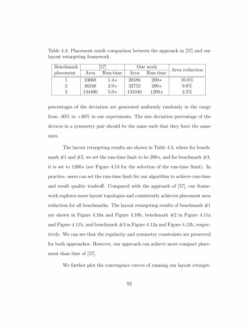
Table 4.3: Placement result comparison between the approach in [57] and ourlayout retargeting framework.
Benchmarkplacement
[57] Our workArea reduction
Area Run-time Area Run-time
1 23068 1.4 s 20586 200 s 10.8%2 36248 2.0 s 32752 200 s 9.6%3 134400 5.0 s 131040 1200 s 2.5%
percentages of the deviation are generated uniformly randomly in the range
from -30% to +30% in our experiments. The size deviation percentage of the
devices in a symmetry pair should be the same such that they have the same
sizes.
The layout retargeting results are shown in Table 4.3, where for bench-
mark #1 and #2, we set the run-time limit to be 200 s, and for benchmark #3,
it is set to 1200 s (see Figure 4.13 for the selection of the run-time limit). In
practice, users can set the run-time limit for our algorithm to achieve run-time
and result quality tradeoff. Compared with the approach of [57], our frame-
work explores more layout topologies and consistently achieves placement area
reduction for all benchmarks. The layout retargeting results of benchmark #1
are shown in Figure 4.10a and Figure 4.10b, benchmark #2 in Figure 4.11a
and Figure 4.11b, and benchmark #3 in Figure 4.12a and Figure 4.12b, respec-
tively. We can see that the regularity and symmetry constraints are preserved
for both approaches. However, our approach can achieve more compact place-
ment than that of [57].
We further plot the convergence curves of running our layout retarget-
92

1
2
3
4
5
6
7
8
9
10
11
12
1314
15
16
17
18
19
20
21
22
232425
26
27
28
29
30 31
32 33
34 35
36 37 38
39
40
41
42
43
44
45
(a)
1
2
3
4
5
6
7
8
9
10
11
12
13
14
15
16
17
18
19
20
21
22
23
24
25
26
27
28
29
30 31
32 3334 35
36 37 38
39
40
41
42
43
44
45
(b)
Figure 4.10: Layout retargeting results of benchmark #1 by (a) [57], and (b)our appoach.
1
2
3
4
5
6
7
8
9
10
11
12
13
14
15
16
17
18
19
20
21
22
23
24
25
26
27
28
29
30
31
32
33
34
35
36
37
38
39
40
41
42
43
44
45
46
47
48
49
50
(a)
1
2
3
4
5
6
7
8
9
10
11
12
13
14
15
16
17
18
19
20
21
22
23
24
25
26
27
28
29
30
31
32
33
34
35
36
37
38
39
40
41
42
43
44
45
46
47
48
49
50
(b)
Figure 4.11: Layout retargeting results of benchmark #2 by (a) [57], and (b)our appoach.
93

1
2
3
4
5
6
7
8
9
10
11
12
13
14
15
16
17
18
19
20
21
22
23
24
25
26
27
28
29
30
31
32
33
34
35
36
37
38
39
40
41
42
43
44
45
46
47
48
49
50
51
52
53
54
55
56
57
58
59
60
61
62
63
64
65
66
67
68
69
70
71
72
73
74
75
76
77
78
79
80
81
82
83
84
85
86
87
88
89
90
91
92
93
94
95
96
97
98
99
100
101
102
103
104
105
106
107
108
109
110
111
112
113
114
115
116
117
118
119
120
121
122
123
124
125
126
127
128
129
130
131
132
133
134
135
136
137
138
139
140
141
142
143
144
145
146
147
148
149
150
151
152
153
154
155
156
157
158
159
160
161
162
163
164
165
166
167
168
169
170
171
172
173
174
175
176
177
178
179
180
181
182
183
184
185
186
187
188
189
190
191
192
193
194
195
196
197
198
199
200
(a)
1
2
3
4
5
6
7
8
9
10
11
12
13
14
15
16
17
18
19
20
21
22
23
24
25
26
27
28
29
30
31
32
33
34
35
3637
38
39
40
41
42
43
44
45
46
47
48
49
50
51
52
53
54
55
56
57
58
59
60
61
62
63
64
65
66
67
68
69
70
71
72
73
74
75
76
77
78
79
80
81
82
83
84
85
8687
88
89
90
91
92
93
94
95
96
97
98
99
100
101
102
103
104
105
106
107
108
109
110
111
112
113
114
115
116
117
118
119
120
121
122
123
124
125
126
127
128
129
130
131
132
133
134
135
136137
138
139
140
141
142
143
144
145
146
147
148
149
150
151
152
153
154
155
156
157
158
159
160
161
162
163
164
165
166
167
168
169
170
171
172
173
174
175
176
177
178
179
180
181
182
183
184
185
186187
188
189
190
191
192
193
194
195
196
197
198
199
200
(b)
Figure 4.12: Layout retargeting results of benchmark #3 by (a) [57], and (b)our appoach.
ing framework on all benchmarks in Figure 4.13. In Figure 4.13, the run-time
is plotted in logarithmic-scale. In Figure 4.13a and 4.13b, the run-time unit
is in “s”, while in Figure 4.13c the run-time unit is in “min.”. The blue lines
are the convergence curves of our framework, and the red lines indicate the
result area of the approach in [57], which is also the initial starting point used
by our placement engine. Although the approach in [57] finishes in a shorter
period of time, it only returns one result with the same layout topology as
the existing layout, which limits the solution space and may lead to inferior
results. Currently, only symmetry and regularity constraints are captured in
our method. Other features that are important to AMS circuits (e.g., signal
integrity) should also be considered as the future work.
94

2 5 20 40 200300 600
Log-scale run-time (s)
20000
20500
21000
21500
22000
22500
23000
23500A
rea
(a)
2 5 20 40 200300 600
Log-scale run-time (s)
31000
32000
33000
34000
35000
36000
37000
Are
a
(b)
0.1 5 10 20 40 60
Log-scale run-time (min.)
126000
128000
130000
132000
134000
136000
Are
a
(c)
Figure 4.13: Layout retargeting result area and run-time tradeoff of benchmark(a) #1, (b) #2, and (c) #3.
4.6 Summary
In this chapter, we extract and explore the layout constraints and pre-
serve the design expertise in the previous high-quality AMS IC layouts. Besides
considering symmetry constraints as in the prior works, we further develop an
efficient sweep line-based algorithm to extract the regularity constraints in an
AMS circuit placement. We also propose a novel analog layout retargeting
95

framework based on the extracted constraints, which can provide more flex-
ibility and achieve better placement quality. Experimental results show the
effectiveness of the proposed techniques.
96

Chapter 5
WellGAN:
Generative-Adversarial-Network-Guided Well
Generation for Analog/Mixed-Signal Circuit
Layout
The preceding chapters mainly focus on the problems and challenges
in the analog placement stage. In contrast, this chapter studies and aims to
resolve the well island generation problem in the post-placement optimization
stage of the analog/mixed-signal circuit layout design flow.
5.1 Introduction
Analog/mixed-signal (AMS) integrated circuit (IC) layout design re-
lies heavily on human experience due to the lack of effective optimization
approaches. Current AMS layout automation tools would generate solutions
inconsistent with designer behavior. Practically, with such solutions, it would
require significant overhead to unravel and debug the problematic chips if any
This chapter is based on the following publication: Biying Xu, Yibo Lin, Xiyuan Tang,Shaolan Li, Linxiao Shen, Nan Sun and David Z. Pan, “WellGAN: Generative-Adversarial-Network-Guided Well Generation for Analog/Mixed-Signal Circuit Layout, ” ACM/IEEEDesign Automation Conference (DAC), 2019. I am the main contributor in charge of prob-lem formulation, algorithm development and experimental validations.
97

failure happens. As a consequence, automatic AMS layout tools have not
been widely adopted. Therefore, it is highly desirable to develop practical
AMS layout tools following designer experience and esthetics to ensure chip
functionality and performance after tape-out.
Well layers are crucial mask layers that define the doping area serving
as the bulk of MOSFETs. Thus, well generation is essential in establishing the
bulk regions which will affect the subsequent optimization stages. Different
from a digital circuit layout where the well regions are pre-designed in the
standard cell layouts and automatically connected through cell abutting, well
regions for analog layouts usually need to be distinctively drawn. Although
some process design kits (PDKs) provide parametric cells with pre-drawn well
regions, these preliminary shapes often need to be properly connected by ex-
tending the well regions or inserting well contacts and routing to pass layout
versus schematic (LVS) and design rule check (DRC). Well generation can in-
fluence the layout compactness and the routing complexity due to the well
spacing and the interconnection of well contacts. Moreover, the geometry of
wells can influence the well proximity effect (WPE) [71], the substrate noise
coupling [25], etc., potentially degrading the performance and robustness of
AMS circuits. Given the above constraints, manual AMS layout well gener-
ation practice generally requires careful design with designer experience and
insights to ensure the circuit functionality and robustness. The manual lay-
out of a two-stage miller-compensated operational amplifier (op-amp) shown
in Figure 5.1 and Figure 5.2 provide an example of such practice, where the
98

capacitors are omitted to conserve space.
While the placement and routing problems for AMS circuits have been
actively explored recently [45,71,74,99], well generation remains an unresolved
challenge. Prior work [11] generated wells with a series of simple computa-
tional geometry operations, including geometric expansion and union. More
recent works [65, 71] imposed rectangular-shaped constraints during well gen-
eration. Nevertheless, the previous approaches didn’t consider the designer
expertise to guide the well region optimization. Recent advances in deep learn-
ing have achieved great success in learning domain-specific knowledge from
existing images and generating new ones mimicking the learned styles [20,63].
The techniques have been widely applied to image generation, image-to-image
translation, etc. Thus, it would be highly beneficial if the layout automation
tools can learn the designer experience and expertise brought by the existing
high-quality manual designs leveraging deep learning techniques.
In this chapter, we propose WellGAN, a generative adversarial network
(GAN) guided well generation framework. Given the previous high-quality
manual layouts by experienced designers, WellGAN attempts to incorporate
the designer expertise by mimicking their layout behavior via a conditional-
GAN model. With a lightweight post-refinement, we are able to generate wells
close to manual designs. Our main contributions are summarized as follows:
• A GAN-guided well generation framework which incorporates designer
expertise by leveraging previous quality-proven manually-crafted layouts
99

VDD
VBP
VBNVBN VBNCMFB
VIP VIN
VOP VON
VDD
VBN
VBP
IBIAS
VDD
VCMVOPVON
VBP VBP
CMFB
Gain Path
Bias Common-mode Feedback
Figure 5.1: Op-amp circuit example.
is presented.
• To the best of our knowledge, this is the first work to apply deep learning
techniques to guide the AMS layout well generation process.
• An effective post-refinement algorithm is also developed to satisfy design
rules following the guidance of solutions generated by GAN.
• Experimental results show that the proposed technique is able to gener-
ate wells close to manual designs.
100

N-Well Bias
and Stage 1
N-Well Stage 2 &
Nulling Resistor
N-Well
Common mode
Feedback
Figure 5.2: Op-amp layout example.
The rest of this chapter is organized as follows: Section 5.2 introduces
the preliminaries and the well generation problem. Section 5.3 explains the
details of WellGAN. Section 5.4 shows the experimental results. And finally,
Section 5.5 summarizes the chapter.
5.2 Preliminaries
Figure 5.3 shows a typical back-end design flow for AMS circuits. As an
essential step in post-placement optimization, well generation takes the place-
ment result as input to establish the bulk regions. In this work, by assuming
manually-crafted layouts from experienced designers have guaranteed superior
performance and robustness, our goal is to leverage a GAN model to generate
101

Placement
Routing
Post-Placement Refinement
Well Generation
Guard Ring and Well/Substrate Contact Insertion
Post-Routing Refinement
Net Shielding
Layout Result
Device Generation
Figure 5.3: A typical back-end design flow for AMS circuits.
wells as close to the manual designs as possible. The formal definition of the
GAN-guided well generation problem is shown in Problem 5.
Problem 5 (GAN-Guided Well Generation). Given the device placement re-
sult, the objective of the GAN-guided well generation problem is to generate
the well regions following the guidance of GAN to minimize the differences
between the generated well regions and manual designs, with the constraints of
correct electrical connections and clean design rules.
The well generation results shall satisfy two constraints, i.e., correct
LVS for electrical connections and clean design rules. LVS correctness must
ensure all the devices that should be covered by the wells are enclosed, and
102

that the well regions should not overlap the devices which are not supposed
to be covered. There are various design rules in well generation including the
minimum spacing, enclosure, width, and area rules. The minimum spacing
rules specify the minimum distance between the well and the objects outside
of it. The minimum enclosure rules specify that the well edges should keep
certain distance from the objects enclosed by the well. The minimum width
rules require that the length of any edge and the distance between any two
edges of a well should be no less than a certain value. Finally, the minimum
area rules suggest the enclosing area of the well should be no less than a certain
value.
Without loss of generality, the scope of this work is the case where
a single type of well is used for layout, e.g., N-well, and the wells share the
same potential so that they can be merged without violating the electrical
connections. Note that, our techniques are general and can be extended to
handle double/triple well processes and different well potentials with minor
modifications, which will be introduced in Section 5.3.2.
5.3 The WellGAN Algorithm
This section will introduce the overall flow, data representation and
preprocessing, together with the detailed algorithms in WellGAN.
103

5.3.1 Overall Flow
As illustrated in Figure 5.4, the WellGAN flow takes the placement
result as input and produces the layout result with generated wells as output.
The flow consists of two phases: training and inference. The training phase is
shown with dashed arrows, where an AMS circuit layout database is utilized
to build a conditional-GAN model for the inference. The inference phase is
indicated with solid arrows, where the GAN model predicts the well region
guidance for the input, and the post-refinement stage generates legal well
regions. The entire flow requires the implementations of the following major
tasks: (1) Preprocessing and extracting layout data for learning. (2) Designing
and training a GAN model leveraging the layout database, which will guide the
well generation at inference time to produce close-to-manual well generation
results. (3) Performing a post-refinement step to legalize the resulting layout.
We have built a database of AMS circuit layouts for our GAN-guided
well generation task, which will be described in Section 5.4 in detail. All of the
layouts in our database satisfy the assumption of this work: (1) a single type
of wells (N-well) is used, and (2) the wells share the same electric potential.
5.3.2 Data Representation and Preprocessing
Raw layouts in the database require special processing before they can
be used as data samples in our learning model. The key techniques include
customized data representation and preprocessing to abstract the data.
Data Representation. The data representation scheme has a tremen-
104

Post-Refinement
Data Preprocessing
Trained GAN Model
GAN-based Well Guiding Region Creation
Wel
lGA
NFr
amew
orkAMS Circuit
Layout Databse
Placement Result
Layout Result w/ Wells
GAN Model
Building
Dashed: trainingSolid: inference
Figure 5.4: Proposed well generation framework (WellGAN).
dous impact on the GAN behavior. The key components that may impact our
well generation are the locations of the devices both with N-wells (e.g., PMOS
and certain types of capacitors, etc.) and without N-wells. The device place-
ment result is composed of various layers, including polysilicon, diffusion, etc.
We choose the oxide diffusion (OD) layers as the input patterns, as they are
common among most devices in our layout database. Other irrelevant layers
are omitted to reduce the effect of noise during training. To preserve the geo-
metric and spatial relationship, we encode the layout patterns into red-green-
blue (RGB) channels of images, which contain adequate information and are
friendly for visualization. Note that as an extension to our framework, more
105

channels can be added to handle more well types and different well potentials.
The red channel covers all the OD patterns within the wells; the green channel
covers all the OD patterns outside of the wells; and the blue channel encodes
the wells. Thus, the inputs are images with patterns only in R and G channels,
and the output images contain patterns in all RGB channels.
Data Preprocessing. To prepare the data samples, it is necessary
to extract the OD layer patterns and differentiate the ones which are covered
by wells and the others which are not. We perform geometric intersection
and subtraction operations on the well layer and the OD layer geometries to
obtain the two types of patterns, respectively. Note that we consider both
the analog and customized digital parts in the AMS circuits, as we observe
the GAN model generates high quality guidance for both. Furthermore, since
the layout dimensions vary from design to design, we apply clipping, zero-
padding, and scaling to transform the layouts into equally-sized image clips
to facilitate the modeling. The clip size and scaling factor are determined in
a way that there are sufficient layout patterns inside each clip and that the
resolution (precision) loss caused by scaling is acceptable. Detailed settings
will be explained in the experimental results section.
5.3.3 GAN-based Well Guidance Generation
Recently, GANs [21] have shown promising potential in many applica-
tions, including image processing, computer vision, and design for manufac-
turability, etc. [29, 102]. A conventional GAN architecture is diagrammed in
106

Figure 5.5. It simultaneously trains two models: a generative model G and
a discriminative model D. The generator G tries to capture the distribution
over the training data y to deceive D, while the discriminator D learns to
distinguish between the “real” samples coming from the training data and the
synthetic samples from G. In a conventional GAN, G is trained to map a ran-
dom noise vector z ∼ pz (which is the distribution of the random noise) to the
data space, with the objective to maximize the probability that D classifies
the samples from G as “real” data:
Ez∼pz [log D(G(z))]
In contrast, D is trained to maximize the probability of assigning correct labels
to the samples:
Ey∼pd [log D(y)] + Ez∼pz [log(1−D(G(z)))]
where pd is the distribution of the dataset. However, for our well generation
problem, we are given the placement results containing the layout patterns.
Therefore, instead of mapping from the random noise to the output, we are
looking for a mapping from the input layout patterns to the layout with wells.
The conventional GAN architecture is thus not directly applicable to our well
generation task.
Conditional GAN (CGAN) [29,63] is a type of GAN architectures that
learns a conditional generative model as depicted in Figure 5.6. Different from
the conventional architecture, both the generator G and discriminator D see
107

randomnoise vector
G
… …
D
real data sample
synthesized sample
or
probabilityof real or fake
Figure 5.5: Architecture of a conventional GAN.
the additional input x. Apart from the random noise z, G also observes x,
and it learns a mapping from both z and x to the output y. The loss function
of the CGAN is in Equation 5.1.
LCGAN(G,D) = Ex,y∼pd(x,y)[logD(x, y)]
+ Ex∼pd(x),z∼pz [log (1−D(x,G(x, z)))]
+ λL1Ex,y∼pd(x,y),z∼pz [||y −G(x, z)||1].
(5.1)
And the objective of CGAN is as follows:
minG
maxDLCGAN(G,D)
The first two terms of LCGAN are similar to the conventional GAN loss function
where G tries to minimize the objective against D that tries to maximize it.
The third term is the L1−norm, which is used to encourage less blurring. Since
our well generation problem is conditioned on the input layout patterns, the
CGAN architecture is suitable.
Our generator and discriminator architecture designs are adapted from
108

randomnoise vector
G
… …
D
probabilityof real or fake
real data sample pair
synthesized sample pair
or
Figure 5.6: Architecture of a CGAN.
[29] and [77]. One characteristic of our well generation task is that our input
and output share common structures which are aligned, e.g., the geometries in
the placement result. In view of this, instead of using a conventional encoder-
decoder [28] structure for our generator design (Figure 5.7a), we embrace an
encoder-decoder with skip connections that follows the U-Net structure [79]
(Figure 5.7b). This allows the low-level information to bypass the bottleneck
layer in the encoder-decoder network and directly shuttle to the layers closer
to the output.
The CGAN training process alternates between gradient descent steps
on G and D, while during inference, only G is run to generate the output. In
our implementation, we employ mini-batch stochastic gradient descent (SGD)
and solve it with the Adam method [35]. In practice, previous work [29] has
demonstrated that the noise vector is typically ignored by G. Hence, in our
experiments, noise is introduced through dropout in the generator instead.
109

…downsample upsample
(a)
…
skip connections(b)
Figure 5.7: (a) Conventional encoder-decoder architecture, and (b) Encoder-decoder with U-Net-like skip connections.
5.3.4 Post-Refinement
During the usage of our well generation framework, the placement result
is preprocessed and input to the trained GAN model to produce the well
guiding regions. We then perform post-refinement to legalize the wells based on
these guiding regions, such that the results satisfy the design rules applicable
to the well layer, including minimum spacing, enclosure, width, and area rules.
In our post-refinement, we first merge the GAN-output images of all the clips
into a single image. After that, we perform computational geometry operations
to refine our results, and convert the obtained polygons back to the final well
regions in the layout. The refinement process is discussed in the following.
5.3.4.1 Rectilinearization
The well guiding regions generated by the trained GAN model are es-
sentially polygons. By extracting the image channel corresponding to the well
layer and transforming it to a binary image through thresholding, we can di-
110

rectly apply the classical border following algorithm in image processing [85] to
find the polygons (contours) defining the guiding regions. Since it is illegal to
have arbitary shapes for wells, we need to transform our results to rectilinear
polygons.
Our rectilinearization algorithm is described in Algorithm 7. First,
we assign either horizontal or vertical directions to the polygon edges based
on their slope (lines 14-16). If the absolute value of the slope of an edge is
less than 1, it is categorized as closer to the horizontal direction. Otherwise,
the edge is assigned to the vertical direction. We then iteratively merge the
neighboring edges with the same assigned direction, such that the sequence of
edges alternates between horizontal and vertical directions. Subsequently, the
merged edges are rectilinearized. The locations of the rectilinearized edges are
determined according to the average coordinates of the points on the curve
along the specific direction (lines 17-21). Afterwards, the resultant rectilin-
earized edges are connected to form the rectilinear polygon. As an example,
Figure 5.8b is the rectilinearization result for the well guiding regions shown
in Figure 5.8a.
5.3.4.2 Legalization
Since the rectilinearized polygons defining the well regions may suffer
from design rules violations, it is imperative to legalize them. For each recti-
linearized well region, the devices outside of it expanded by minimum spacing
are first subtracted from it. Then, it is unioned with the devices inside it
111

Algorithm 7 Rectilinearization.
Input: Polygon pOutput: Rectilinearized polygon pr
1: E ← vector of edges of p, Enew ← ∅2: for all e ∈ E do3: if AssignEdgeDirection(e) == Enew.last.dir then4: merge e with Enew.last5: else6: Enew ← Enew ∪ e7: end if8: end for9: merge Enew.f irst with Enew.last if same direction
10: for all e ∈ Enew do11: e.loc ← getLocation(e)12: end for13: pr ← polygon formed by Enew
14: function AssignEdgeDirection(e)15: return |slope(e)| ≥ 116: end function
17: function getLocation(e)18: A ← area under the curve formed by points of e19: d ← distance b/w the first and last points of e20: return A/d21: end function
expanded by minimum enclosure.
To address the minimum width design rule violations, we propose the
algorithm presented in Algorithm 8. The algorithm works by mapping and
aligning the polygon edges to a grid whose grid size equals to the specified
minimum width, as illustrated in Figure 5.9. Each polygon builds its own grid.
The algorithm will make decisions on which grid each edge should be aligned
112

(a) guiding region (b) rectilinearized (c) legalized
Figure 5.8: Example post-refinement results after each step.
to. It will first try to align the edge to the nearest grid, if the location does not
incur the minimum enclosure nor spacing rule violations. Otherwise, it will
try to align the edge to the other side which would cause no violation. If that
is again infeasible, the algorithm will choose to align to the grid which satisfies
the minimum enclosure rules, and leave the minimum spacing violations to be
fixed at a later stage. For example, edge e in Figure 5.9 is aligned to location e′
to satisfy the enclosure requirement. Empirically, since the minimum width is
small compared to the size of the wells and the devices, we are able to align to
the grids without violating the spacing and enclosure rules for all the layouts
in our test set.
Algorithm 8 can guarantee to resolve all the minimum width violations
after aligning to grids since no edge will have length less than the grid size
which is the specified minimum width, neither will the edge distances. It will
not cause minimum enclosure rule violations, either. Besides, the minimum
area rule can be easily checked by calculating the area of each well region. Since
113

Legalized well region
Well region before legalization
Placement objects inside the well
Placement objects outside of the well
Gridsee’ violation!
Figure 5.9: Grid-based method for the minimum width rule legalization.
the minimum enclosure rule ensures that the wells containing any device will
be larger than the required minimum area, the wells violating the minimum
area rule shall not contain any device, thereby they can be simply removed to
fix the violations.
As discussed previously, although we completely eliminate the mini-
mum width, enclosure, and area rule violations, there might still exist mini-
mum spacing rule violations. To settle the spacing violations, a linear program-
ming formulation can be employed based on the constraint graphs to spread
the devices and wells, with the objective of displacement minimization, which
is widely adopted for placement legalization [12]. Details are omitted here to
conserve space. The example of a legalization result is shown in Figure 5.8c.
5.4 Experimental Results
All of our algorithms are implemented in Python and C/C++, and
the experiments are performed on a Linux server with 3.3 GHz Intel i9 CPU,
128GB memory, and one Nvidia Titan Xp GPU. The generative adversarial
114

Algorithm 8 Legalization.
Input: Polygon p, minimum width Wmin
Output: Legalized polygon pl1: build grids with size Wmin
2: for all edge e ∈ p do3: if nearest grid is feasible then4: align e to the nearest grid5: else if second nearest grid is feasible then6: align e to the second nearest grid7: else8: align e to the grid satisfying min. enclosure rules9: end if
10: end for
net is developed based on TensorFlow [2] library. To build our database for
well generation, we gather 131 distinguished silicon-measurement-proven AMS
circuit layouts (in GDSII format) from the taped-out chips in TSMC 40nm
process technology. The layouts are split into a total of 881 clips, with each
layout clip transformed into a 256-by-256 RGB image (as in Section 5.3.2).
Random selection of 80% clips are used for training and the remaining 20%
form the test set. Note that all the clips belonging to the same circuit shall be
allocated to the same set, so that during inference we can recover the entire
layout for the test circuit solely from the test set. We implement the algorithm
in [11] as the baseline for comparison. It performs union on the devices inside
the well expanded by certain distance.
The training is run for 100 epochs with a mini-batch size of 1. After
that, we run the inference flow on the test dataset with the trained model.
We compare WellGAN with the baseline algorithm on the same dataset. Both
115

algorithms are very efficient, i.e., within a few seconds for a typical layout size.
The visualization of the well generation results of several test circuit exam-
ples are shown in Figure 5.10, where “golden” means the manual layouts by
experienced designers, “guidance” refers to the well guiding regions output by
our GAN model, “ours” means the final well generation results from WellGAN
after post-refinement, and “baseline” refers to the results of the baseline algo-
rithm. Figure 5.10a shows the results for circuit A, and Figure 5.10b are for
circuit B, etc. Recall that blue channel encodes the wells and the other chan-
nels are the input patterns. From the test results, we can see that WellGAN
is able to successfully mimic the designers’ behavior from the manual layout
data.
To quantify the similarity between the results, the metric we use is
the Manhattan norm of the element-wise (pixel-by-pixel) difference between
two images on the blue channel which represents the well regions. If the two
images have different sizes due to spacing rule settling, the smaller image is
center-aligned with the larger one and is zero-padded for comparison. The
norm is calculated as the summation of the absolute values of the difference
for all pixels divided by the image size. The distribution of the Manhattan
norm of the element-wise difference over a total of 43 test circuits is plotted in
Figure 5.11. The x-axis is the range of the Manhattan norm of the element-wise
difference, and the y-axis represents the frequency that the norm of difference
occurs in the test results. For example, 19% of the test results for WellGAN
are within a difference of 0 to 2% from the manual layouts, whereas only 5%
116

of the baseline results fall in this range. From the figure, we can see that
the difference of the majority of our results are within a small scale, while
the baseline algorithm may result in larger differences (up to 44% as shown
in the histogram). Our element-wise difference distribution demonstrates a
smaller mean and standard deviation than the baseline, as shown in Table 5.1.
Moreover, our results are free from minimum spacing, enclosure, width, and
area design rule violations.
To evaluate the routing complexity, we count the number of wells gen-
erated by both WellGAN and the baseline for all test circuits. A larger number
of wells means more well contacts to be connected by routing, thereby poten-
tially increasing the routing complexity. Our results show that on average,
the number of wells generated by the baseline is 75% more than WellGAN.
This demonstrates that our well generation results are expected to have better
routability.
Furthermore, we compare the post-layout circuit performance simula-
tion results between the layout with our generated wells and the manual one
for the op-amp circuit (see Figure 5.1), as shown in Table 5.2. The placement
is the same for both layouts, while routing is slightly different due to different
well contact locations. The WellGAN-generated layout circuit performance
is comparable to the manual design. Nonetheless, the well generation result
from the baseline requires dramatic change to both placement and routing to
accommodate the increased number of well contacts, thus the comparison is
less meaningful.
117

manual guidance ours baseline
(a) Circuit A
manual guidance ours baseline
(b) Circuit B
manual guidance ours baseline
(c) Circuit C
manual guidance
ours baseline
(d) Circuit D
Figure 5.10: Test circuit examples A, B, C, and D.
118

0-2 2-4 4-6 6-88-1010
-1212
-1414
-1616
-1818
-2020
-2224
-2636
-3838
-4040
-4242
-44
Manhattan norm of element-wise difference (%)
0.0
0.1
0.2
0.3
Freq
uenc
y WellGANBaseline
Figure 5.11: Distribution of the Manhattan norm of the element-wise differ-ence.
Table 5.1: Statistics of the Manhattan norm of element-wise difference for thetest results.
Metric WellGAN Baseline
Mean 5.64% 12.65%Standard Deviation 3.58 10.25
Table 5.2: Post-layout simulation results of the op-amp layout with wells gen-erated by WellGAN.
DesignUnity Gain
Bandwidth (MHz)Phase Margin
()Loop Gain
(dB)
Manual 103.70 71.89 36.33Ours 104.64 65.38 37.61
5.5 Summary
Well generation is a fundamental challenge in back-end AMS design
flow. This work attempts to generate wells by mimicking experienced design-
ers’ behavior from high-quality manually-crafted layouts. A holistic well gen-
eration framework, WellGAN, is proposed, with GAN-guided well geometry
119

guidance generation and post-refinement. Experimental results demonstrate
the proposed framework is able to generate wells close to manual designs with
comparable circuit performance.
120

Chapter 6
A Scaling Compatible, Synthesis Friendly
VCO-based Delta-sigma ADC Design and
Synthesis Methodology
The prior chapters have resolved the challenges in the optimization-
based and template-based analog/mixed-signal integrated circuit layout au-
tomation approaches. For the standard cell-based approach, this chapter
presents a scaling compatible, synthesis friendly ∆Σ ADC design and its syn-
thesis methodology.
6.1 Introduction
The conventional way to design analog/mixed-signal (AMS) circuits
relies heavily on the use of operational amplifiers (opamps) to process signals in
This chapter is based on the following publications:
1. Biying Xu, Shaolan Li, Nan Sun, and David Z. Pan, “A Scaling Compatible, Syn-thesis Friendly VCO-based Delta-sigma ADC Design and Synthesis Methodology, ”ACM/IEEE Design Automation Conference (DAC), 2017.
2. Shaolan Li∗, Biying Xu∗, David Z. Pan and Nan Sun, “A 60-fJ/step 11-ENOB VCO-based CTDSM Synthesized from Digital Standard Cell Library, ” (∗ Equally Con-tributed) IEEE Custom Integrated Circuits Conference (CICC), 2019.
I am the main contributor in charge of problem formulation, algorithm development andexperimental validations.
121

the voltage domain (VD). The well-established VD AMS design methodology
encounters severe difficulties in advanced nanometer-scale CMOS process due
to reduced supply voltages and transistor intrinsic gains. For instance, as the
transistor feature size shrinks from 0.5um to 22nm, the transistor intrinsic
gain drops from 180 to 6, and the supply voltage decreases from 5V to 1V
(see Figure 6.1a) [1]. Conventional VD-AMS architectures depend on the high
gain of opamps to guarantee precision and linearity; however, the required high
gain is very difficult to achieve with a small transistor intrinsic gain. A low
supply voltage further increases the difficulty, as it prevents the use of many
gain boosting techniques that require stacking transistors vertically. Hence,
long-channel thick-oxide transistors and high supply voltages have to be used
for VD-AMS, resulting in limited performance enhancement and area/cost
reduction as technology advances, in contrast to their digital counterparts.
The advent of nanometer CMOS technology calls for a new AMS frame-
work that not only does not suffer from scaling but actually benefits from it.
As shown in Figure 6.1b, one clear merit of CMOS scaling is that the transistor
speed, as characterized by fT , has increased from 16 GHz at 0.5um to 400 GHz
at 22nm. The timing resolution, as represented by the fan-out-of-4 (FO4) delay
of an inverter, has also improved from 140ps to 6ps. As a result, it is promis-
ing to process analog information in the time domain (TD) or phase domain
instead of in VD, leading to the concept of TD-AMS. TD-AMS framework has
been adopted among a wide range of AMS circuits [15,34,40,82,86,104]. They
care less about VD accuracy, obviating the need for opamps. The integra-
122

0
50
150
22324565901301802503505001
2
3
4
Gate length [nm]
Tra
nsis
tor
intr
insic
ga
in
Po
we
r su
pp
ly [
V]
200
100
5
(a)
0
20
40
60
80
100
120
140
0
50
100
150
200
250
300
350
2232456590130180250350500Gate length [nm]
Fo
4 d
ela
y [
ps]
f[G
Hz]
T
160 400
(b)
Figure 6.1: (a) Power supply and transistor intrinsic gain scaling trend. (b)fT and FO4 delay trend.
tion in the phase domain is performed by a ring voltage-controlled oscillator
(VCO), and the phase comparison can be realized using an XOR gate. They
are area/power efficient, operate well under low voltage, and their performance
improves as the inverter delay decreases and the timing resolution increases
with the advance in process technology. Therefore, TD-AMS is a promising
scheme which enjoys superb scaling compatibility.
In addition to the challenge posed by CMOS scaling, another key limi-
tation for conventional AMS circuit design is low productivity. Although much
progress has been made by electronic design automation (EDA) researchers on
the automatic layout design for AMS circuits [19,22,38,46,59,73,99], the tools
are still immature and have not been widely used in practice. The majority of
the AMS layout design efforts are still handled manually. Recently, some early
attempts (including ADCs [89–91], phase-locked loop (PLL) [13], filters [55])
have been made to design AMS circuits to be digital-like and reasonably robust
123

Manual Layout
Design Conventional VD-AMS Circuit
Result
Circuit Specifications
(a)
Synthesize Layout
Design Novel Synthesis Friendly
TD-AMS Circuit
Result
Circuit Specifications
(b)
Figure 6.2: (a) Conventional VD-AMS circuits design flow. (b) Novel synthesisfriendly TD-AMS circuits design flow.
to layout effects (e.g. mismatches), so that they can be described in Hardware
Description Languages (HDLs) and synthesized using digital layout synthesis
tools. Such synthesis friendly AMS circuit design and synthesis methodology
greatly improves design productivity and reliability, reduces design cost, as
well as shortens product turn-around time and time-to-market compared with
the conventional AMS circuit design flow (see Figure 6.2a and Figure 6.2b).
This is because not only the layout synthesis becomes substantially easier, but
describing AMS circuit in HDL also greatly enhances circuit portability.
Ultra-low-power and ultra-low-voltage ADCs compatible with CMOS
scaling are in increasingly high demand by emerging applications, including
internet-of-things (IoT), autonomous wireless sensor networks (WSN), and
biomedical implants. While the ADCs presented in [89–91] are fully digitally
synthesizable, they did not achieve desirable circuit performances (e.g. Walden
124

figure-of-merit (FOM) [88], signal-to-noise and distortion ratio (SNDR)) nor
demonstrate scalability. In this work, for the first time, we present a novel
scaling compatible, synthesis friendly TD VCO-based continuous-time (CT)
delta-sigma (∆Σ) ADC whose performance improves as technology advances.
Decomposed into digital gates (e.g. inverters) and a small set of simple cus-
tomized cells (e.g. resistors), its layout is fully synthesizable by leveraging
digital layout synthesis tools. Our main contributions are summarized as fol-
lows:
• This is the first work to design a highly scaling compatible TD VCO-
based continuous-time ∆Σ ADC to be fully synthesis friendly;
• A significant productivity improvement to AMS circuit layout is obtained
with our proposed design and synthesis methodology;
• Our circuit performance compares favorably with previous works on syn-
thesis friendly ADC design, and excellent scaling compatibility is demon-
strated.
The rest of this chapter is organized as follows: Section 6.2 gives the
complete circuit design of the scaling compatible, synthesis friendly VCO-
based ∆Σ ADC. Section 6.3 presents the layout synthesis methodology for our
designed circuit. Section 6.4 shows the experimental results. Finally, Section
6.5 summarizes the chapter.
125

6.2 Circuit Design
6.2.1 Preliminary of Delta-sigma ADC
The block diagram of a ∆Σ ADC is shown in Figure 6.3. By placing
the quantizer in a feedback loop that contains a high-gain, low-pass loop filter,
the quantization error appears at the output can be high-pass shaped. With
subsequent low pass filtering and decimating in digital domain, the effect of
quantization to the in-band signal can be suppressed. Therefore, ∆Σ ADC
facilitates us to use a low resolution, easy-to-build quantizer to achieve high
resolution conversion. This type of ADC is an important building block for
many mobile, audio and radar applications.
Loopfilter
Quantizer+
DAC
Vin(t)-
d[n]
Figure 6.3: Block diagram of a ∆Σ ADC.
6.2.2 Proposed Synthesis Friendly Delta-sigma ADC
Figure 6.4 shows the architecture of the proposed ∆Σ ADC. It is di-
vided into slices, where the number of slices is selected according to the effective
quantizer resolution requirement. Each slice can be decomposed into simple in-
dependent circuit building blocks, including an XOR gate, a digital-to-analog
converter (DAC), retiming latches, ring VCOs, buffers, and comparators. The
126

VCO stage which works as an integrator can be simply built by 4 cross-coupled
inverters (see Figure 6.5). The buffer, which is similar to the VCO stage ex-
cept that it has a fixed bias tail, is used to isolate kickback noise [104]. The
comparator samples the output of the replica buffer. Because of its simple
structure, the proposed ADC allows easy adaptations to different specifica-
tions as long as they are within the ADC performance boundary in a given
process. For example, to increase the effective quantizer resolution, we can
simply add more slices. To widen the signal bandwidth, we can increase the
clock frequency. To increase SQNR, we can boost the loop gain by increasing
either the DAC feedback current or the VCO tuning gain. The ability to be
decomposed into simple circuit building blocks (digital gates and resistors) fa-
cilitates the adoption of digital layout synthesis flow. Further detailed circuit
analysis can be found in [40,104].
Besides synthesis friendliness, an additional benefit of the proposed
ADC is its superb scaling compatibility. Firstly, it is relatively robust against
non-idealities, such as device parasitics and mismatches, which are major chal-
lenges in nanometer-scale CMOS process. Both the VCO mismatches and com-
parator offset are high-pass shaped, and thus, hardly affect ADC performance.
Secondly, the timing resolution increases and the performance improves as the
process technology advances, in light of the fact that the delay of the inverters
in the VCO becomes shorter and shorter with CMOS scaling [1]. Moreover,
the proposed ADC also operates well under low voltage. These factors have
made it a favorable choice in the advanced CMOS process.
127

clk
clk
DAC
clk
clk
DAC
clk
clk
DAC
......
......
VINP
VINN
...
VCTRLP
VCTRLN
d1 d2dN
Oneslice
VCO1
VCO2
clk
latch
latch
clk
clk
latch
latch
clk
clk
latch
latch
clk
buffers comparators
Figure 6.4: The proposed scaling compatible, synthesis friendly VCO-based∆Σ ADC architecture.
Vctrl
INP INM
OUTM OUTP
VSS
(a)
INP
INM
Vctrl
OUTP
OUTM
(b)
Figure 6.5: (a) Transistor level schematic of VCO cell. (b) VCO implementedusing digital inverters gates.
128

6.2.2.1 Novel Synthesis Friendly TD Analog Comparator Design
As the VCO nodes switch with relatively low swing (e.g. 0.5V typi-
cally), the sense amplifier flip flops (SAFFs) used to latch the VCO outputs
usually employs a strongARM comparator for robust latching as well as in-
trinsic level shifting. However, conventional strongARM comparators are clas-
sified as AMS circuit and thus not implemented in the standard cell library.
To overcome this issue, [91] proposed to form a comparator with two cross-
coupled 3-input NAND gates, providing a synthesis friendly alternative of the
strongARM comparator. This solution, however, requires the input common
mode (CM) to be sufficiently high. In the proposed ADC, the input of the
SAFF interfaces with the VCO buffer, whose output CM resides at around
only 0.25V. For this reason, we proposed a modified comparator design using
cross-coupled 3-input NOR (NOR3) gates, which easily facilitates low common
mode input. The schematic of a PMOS input strongARM comparator and the
proposed NOR3-based comparator are shown in Figure 6.6a and Figure 6.6b
respectively. We can observe that the NOR3-based comparator resembles the
former. Under 0.25V input CM, the NMOS pair marked in blue are essen-
tially cut off, and thus the proposed comparator is functionally identical to
the strongARM comparator. Noteworthily, as the TD nature of this ADC
desensitized VD related non-idealities such as offset and memory effect, the
default NOR3 layout can be used without special modification and imposing
additional placement and routing (P&R) constraint.
The complete SAFF gate-level schematic is shown in Figure 6.7a. The
129

SR-latch following the NOR3-based comparator provides logic keeping when
the comparator resets.
INP INM
OUTPOUTM
VDD
GND
CLK
CLK CLK
(a)
INP INM
OUTP
OUTM
VDD
GND
CLK
CLK CLK
VDD
GND
CLK
INP INM
3-inputNOR gate
cut off when v is lowcm
(b)
Figure 6.6: (a) Regular TD comparator. (b) TD comparator by connectingtwo 3-input NOR gates.
130

CLK
INM
INP
QP
QM
OUTP
OUTM
(a)
V
V
bias2
V bias1
VCTRLP VCTRLN
DP DN
REFP
(b)
DP
DN
VCTRLP
VCTRLN
VREFP
VREFP
(c)
Figure 6.7: (a) Proposed TD comparator gate-level implementation with SR-latch. (b) A conventional current-steering DAC. (c) The resistor DAC used inour synthesis friendly ADC circuit.
6.2.2.2 Synthesis Friendly DAC Architecture Selection
Synthesizable voltage DAC architecture using basic logic gates has been
previously reported in [13]. Nevertheless, in CT ∆Σ ADC, current DACs are
preferred as it simplifies the feedback network. An example schematic of a
conventional current-steering DAC is shown in Figure 6.7b. This structures
is not readily available in the standard cell library. In addition, an analog
intensive bias generation network is also required for this type of DAC. The bias
network must be manually laid out to guarantee functionality and matching,
thus making current-steering DAC highly synthesis unfriendly. In this work,
131

we propose to use resistor DAC over conventional current-steering structure.
To source current, we connect the resistor between the feedback point and
VREFP . To sink current, we connect the resistor between the feedback point
and ground. This can be simply implemented by a resistor and an inverter, as
illustrated in Figure 6.7c. Hence, we only need to insert a simple cell into the
library representing a resistor fragment and synthesize a DAC through proper
instantiation. As resistors exhibit high raw matching and do not require bias,
P&R requirements are also relaxed for resistor DAC.
6.3 Synthesis Methodology
Previous synthesis friendly AMS circuit design works [13, 55, 89–91]
adopted the digital automatic placement and routing (APR) flow to generate
the layouts by turning off the optimizations that are irrelevant, including logic
optimization, timing optimization, etc. However, this oversimplified paradigm
shows its limitations when applied to the ADC circuit we design. The reason
lies in that the power domains (PDs) and circuit components groups con-
straints were not incorporated into their flow while they are required in our
circuit, which will be further discussed in Section 6.3.3. Hence, this calls for a
layout synthesis methodology for synthesis friendly AMS circuit that is capa-
ble of handling PDs and components groups constraints, motivating our layout
synthesis methodology.
Figure 6.8 shows the overall flow of our approach. The HDL files gener-
ation phase, standard cell library modification phase, together with the floor-
132

Standard Cell Library Modification
Resulting Layout
Floorplan Specification(e.g. .fp file)
Modified Standard Cell Library
(e.g. LEF, GDSII)
HDL Generation
Gate-level Netlist HDL
(e.g. Verilog)
Floorplan Generation
Automatic Place & Route (Digital Circuit)
Figure 6.8: Overall flow of the layout synthesis methodology for the proposedsynthesis friendly ADC.
plan generation phase prepares input data to the APR stage, which include the
gate-level netlist in HDL (e.g. Verilog), files describing the modified standard
cell library (e.g. LEF and GDSII files), as well as the floorplan specification
(e.g. files with the .fp extension used in Cadence Encounter), respectively.
APR is then performed to generate the final layout.
6.3.1 Standard Cell Library Modification
Standard cell library modification phase (see Figure 6.9a) adds a small
set of customized AMS circuit building blocks to the existing digital standard
cell library. As discussed in Section 6.2, the only circuit building blocks that
need to be customized are the resistors, while other building blocks can be
implemented purely with digital gates. Each resistor is decomposed into sev-
133

eral identical fragments and only the fragments are added to the standard
cell library as special “standard cells”, which we call resistors standard cells.
High resistivity usually implies smaller area but lower accuracy, and smaller
fragments often provide more placement flexibility while the routing may be-
come more complicated. We design the resistors standard cells considering
these trade-offs. Once the parameters of the resistors standard cells are deter-
mined, the layout of the resistors can be conveniently drawn from the foundry
provided process design kit (PDK), requiring minimal manual design efforts.
Figure 6.10 gives the layouts of the two customized resistors standard
cells we generate using material with different resistivity. In the figure, the
displayed dimensions of both resistors standard cells are scaled to have the
same width so that both of them can be seen clearly. The actual heights
of both resistors standard cells should be similar to the digital standard cell
height. After that, we can export their layouts in GDSII format, merge them
with the existing standard cell library, and generate the LEF and GDSII files
describing the modified standard cell library.
6.3.2 HDL Generation
The HDL Generation phase converts the circuit netlist from schematic
into a HDL representation. Since it is a common practice to design AMS cir-
cuits in schematic, our synthesis flow exports the circuit netlist designed in
schematic into gate-level HDL (e.g., Verilog) using existing EDA tools (e.g.,
Cadence Virtuoso NC-Verilog). An added benefit is that being able to express
134

Add to Existing Standard Cell Library
Generate Customized Standard Cells
Modified Standard Cell Library (e.g. LEF, GDSII)
(a)
Floorplan Specifications
Floorplanning for Power Domains and Component Groups
Partition the Circuit into Power Domains and Component Groups
(b)
Figure 6.9: (a) Standard cell library modification. (b) Floorplan generation.
the AMS circuit in HDL facilitates the AMS design porting between differ-
ent technology nodes. Two example circuit modules of the designed synthesis
friendly ADC in Verilog is given, with the Verilog description of the com-
parator circuit design shown in Table 6.1, and the top-level Verilog module of
one slice of the ADC shown in Table 6.2. The resulting netlist is in gate-level
instead of register-transfer level (RTL), because the logic synthesis methodolo-
gies designed for digital circuit may not be suitable for AMS circuit. Improper
choices of standard cell sizes by the digital logic synthesis tools may destroy
135

(a)
(b)
Figure 6.10: Generated resistors standard cells layouts: (a) 1 kΩ resistor withlower resistivity. (b) 11 kΩ resistor with higher resistivity.
Table 6.1: Example Verilog implementation of the proposed synthesis friendlycomparator.
1 module comparator(Q,QB,VDD,VSS,CLK,INM,INP)2 inout VDD, VSS;3 input CLK, INM, INP;4 output Q, QB;5 wire OUTP, OUTM;
6NOR3X4 I0 (.Y(OUTP), .VDD(VDD), .VSS(VSS), .A(OUTM), .B(INP),.C(CLK));
7NOR3X4 I1 (.Y(OUTM), .VDD(VDD), .VSS(VSS), .A(OUTP), .B(INM),.C(CLK));
8 NOR2X1 I2 (.Y(Q), .VDD(VDD), .VSS(VSS), .A(OUTP), .B(QB));9 NOR2X1 I3 (.Y(QB), .VDD(VDD), .VSS(VSS), .A(OUTM), .B(Q));10 endmodule
the AMS circuit functionality.
6.3.3 Floorplan Generation
In the proposed ADC circuit, there are several different Power/Ground
(P/G) nets connected to the P/G pins of different standard cells. For example,
the power pins of the inverters in VCO1 is connected to one of the VCO control
nodes VCTRLP (denoted as PD VCTRLP in the figure), while the gates composing
the comparator have their power pins connected to the V DD net (denoted as
136

Table 6.2: Example Verilog implementation of the proposed ADC slice.
1module ADC slice(CLK, IN, IN2, IP, IP2, ON, ON2, OP, OP2, VBUF,VCTRLN, VCTRLP, VDD, VREFP, VSS)
2inout IN, IN2, IP, IP2, ON, ON2, OP, OP2, VBUF, VCTRLN, VCTRLP,VDD, VREFP, VSS;
3 input CLK;4 wire BON, BOP, BON2, BOP2, DB, DAC OUT, DAC OUT B;
5buf cell I0 (.BIN(ON), .BIP(OP), .BON(BON), .BOP(BOP),.VCTRL(VBUF), .VSS(VSS));
6buf cell I1 (.BIN(ON2), .BIP(OP2), .BON(BON2), .BOP(BOP2),.VCTRL(VBUF), .VSS(VSS));
7pd VDD I2 (.BON(BON), .BON2(BON2), .BOP(BOP), .BOP2(BOP2),.CLK(CLK), .D(DOUT), .DB(DB), .VDD(VDD), .VSS(VSS));
8 res cell I3 (.T1(DAC OUT B), .T2(VCTRLN));9 res cell I4 (.T1(DAC OUT), .T2(VCTRLP));
10pd VREFP I5 (.D(DOUT), .DAC OUT(DAC OUT),.DAC OUT B(DAC OUT B), .DB(DB), .VREFN(VSS),.VREFP(VREFP));
11VCO cell I6 (.ON(ON2), .OP(OP2), .VCTRL(VCTRLN), .VSS(VSS),.IN(IN2), .IP(IP2));
12VCO cell I7 (.ON(ON), .OP(OP), .VCTRL(VCTRLP), .VSS(VSS),.IN(IN), .IP(IP));
13 endmodule
PD VDD). The entire circuit can be decomposed into several different PDs
and groups. A power domain consists of the circuit components sharing the
same power supply, while a components group is a group of circuit components
that may not need power supply. Figure 6.11 shows the PDs and components
groups of one slice of the circuit. In conventional digital APR, the P/G rails
of the cells in the same placement row will be connected and short their P/G
pins, which will cause a problem if any two cells in the row are connected to
different P/G nets.
137

One solution to circumvent this problem is to use the multiple supply
voltages (MSV) design capability which is available in most APR tools (e.g.,
Cadence Encounter and Synopsys IC Compiler). The floorplan generation
flow is shown in Figure 6.9b. The digital gates are assigned to different PDs
according to their supply voltag, and the resistors are assigned to different
groups according to the resistor types. Note that a PD or a components group
may be further partitioned into smaller PDs or component groups to increase
the floorplan flexibility.
clk
clk
DAC
VINP
VINN
VCTRLP
VCTRLN
clk
latch
latch
clk
...
...
...
...
PD VDDPD VREFP
PD VCTRLPPD VCTRLN
PD VBUF
Group DAC resistorsGroup inputresistors
Figure 6.11: One slice of the ADC decomposed into different power domainsand floorplan groups.
6.4 Experimental Results
Post-layout simulation is performed for both 40-nm and 180-nm CMOS
process. The simulation takes into account noise and systematic mismatches,
and the architecture is robust against random mismatches as discussed in
Section 6.2.2. The design migration between 40-nm and 180-nm process is
138
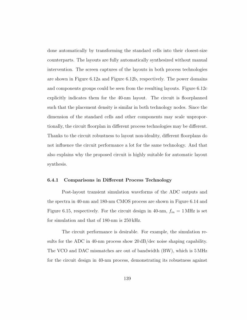
done automatically by transforming the standard cells into their closest-size
counterparts. The layouts are fully automatically synthesized without manual
intervention. The screen captures of the layouts in both process technologies
are shown in Figure 6.12a and Figure 6.12b, respectively. The power domains
and components groups could be seen from the resulting layouts. Figure 6.12c
explicitly indicates them for the 40-nm layout. The circuit is floorplanned
such that the placement density is similar in both technology nodes. Since the
dimension of the standard cells and other components may scale unpropor-
tionally, the circuit floorplan in different process technologies may be different.
Thanks to the circuit robustness to layout non-ideality, different floorplans do
not influence the circuit performance a lot for the same technology. And that
also explains why the proposed circuit is highly suitable for automatic layout
synthesis.
6.4.1 Comparisons in Different Process Technology
Post-layout transient simulation waveforms of the ADC outputs and
the spectra in 40-nm and 180-nm CMOS process are shown in Figure 6.14 and
Figure 6.15, respectively. For the circuit design in 40-nm, fin = 1 MHz is set
for simulation and that of 180-nm is 250 kHz.
The circuit performance is desirable. For example, the simulation re-
sults for the ADC in 40-nm process show 20 dB/dec noise shaping capability.
The VCO and DAC mismatches are out of bandwidth (BW), which is 5 MHz
for the circuit design in 40-nm process, demonstrating its robustness against
139
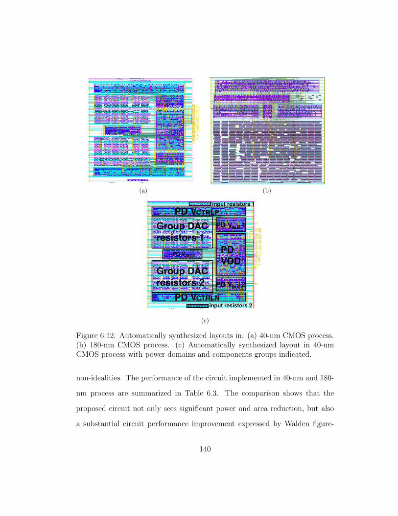
(a) (b)
Group DAC resistors 2
Group DAC resistors 1
PD VDD
input resistors 1PD V CTRLP
PD V 1 BUF
PD V CTRLN
PD V 2 BUF
input resistors 2
PD VREFP
(c)
Figure 6.12: Automatically synthesized layouts in: (a) 40-nm CMOS process.(b) 180-nm CMOS process. (c) Automatically synthesized layout in 40-nmCMOS process with power domains and components groups indicated.
non-idealities. The performance of the circuit implemented in 40-nm and 180-
nm process are summarized in Table 6.3. The comparison shows that the
proposed circuit not only sees significant power and area reduction, but also
a substantial circuit performance improvement expressed by Walden figure-
140

Table 6.3: Performance comparison between 40-nm and 180-nm process.
Process(nm)
fs(MHz)
BW(MHz)
SNDR(dB)
Power(mW)
Area(mm2)
FOM(fJ/conv)
40 750 5 69.5 1.37 0.012 56.2180 250 1.4 69.5 5.45 0.151 798
* ENOB = SNDR−1.766.02 , FOM = Power
2ENOB ·2·BW
of-merit (FOM [88]) when moving from an older technology node to a more
advanced one. Besides, the proposed circuit is also able to work under low
input amplitude. Figure 6.16 shows the circuit performance of the ADC in
40-nm CMOS process working under input amplitude of 10 mV. No idle tones
are observed for the low input amplitude. Further, the power breakdown for
both process technologies is calculated (see Figure 6.13). It can be seen that
the digital portion of the power decreases from 88% to 73%, which is due to
the scaling of the digital portion of the circuit. Since the power consumed
by the digital portion still occupies 73% of the total power, we can expect to
see further power reduction and FOM improvement in more advanced process
due to digital scaling. In contrast to the traditional VD-AMS circuits that is
incompatible with CMOS scaling, the experimental results demonstrate that
the novel TD-ADC enjoys the scaling benefits, and thus is a promising candi-
date to address the critical real-world challenge of cost-effectively integrating
high-performance ADC with digital functions on a system-on-a-chip (SoC).
141

73%
27%
Digital Analog(a)
88%
12%
Digital Analog(b)
Figure 6.13: Power Breakdown of our ADC circuit in (a) 40-nm CMOS process.(b) 180-nm CMOS process.
Figure 6.14: Post-layout transient simulation results of the ADC time-domainoutputs in: 40-nm CMOS process (left), and 180-nm CMOS process (right).
6.4.2 Comparisons with Previous Works
Table 6.4 presents the comparisons of our work with previous works
of synthesis friendly ADCs. Our work achieves the highest SNDR, which is
13 dB higher than the second best. Being able to achieve a high SNDR of
69.5 dB proves that it is robust against mismatches, and thus, enables the use
of digital layout tools for layout synthesis. The overall energy efficiency or
FOM of our synthesized ADC is 56.2 fJ/conv-step under post-layout simula-
142

10 0 10 2
Frequency (MHz)
-120
-100
-80
-60
-40
-20
0
Ampl
itude
(dBF
S)
10 0 10 2
Frequency (MHz)
-120
-100
-80
-60
-40
-20
0
Ampl
itude
(dBF
S)BW
5M
20dB/dec
VCO, DAC mismatch out of band
Figure 6.15: Post-layout simulation results of the ADC spectrum in: 40-nmCMOS process (left), 180-nm CMOS process (right).
Figure 6.16: ADC spectrum and time-domain output with low input amplitudein 40-nm CMOS process.
tion. It compares favorably to the state-of-the-art automatically synthesized
ADCs [89–91]. This demonstrates that the proposed scaling compatible, syn-
thesis friendly ADC design and its synthesis methodology not only significantly
improves design productivity and reduces design cost, but also achieves satis-
143

Table 6.4: Comparisons with previous works.
Metric This work [89] [91] [90]
Supply voltage (V) 1.1 1 1.2 1.2 1.3Process (nm) 40 65 130 90 180
fs (MHz) 750 150 80 210 50BW (MHz) 5 2.34 2 105 25SNDR (dB) 69.5 56.3 56.2 35.9 34.2Power (mW) 1.37 0.872 0.983 34.8 0.433Area (mm2) 0.012 0.014 0.046 0.18 0.094
FOM (fJ/conv) 56.2 348.6 466 3255 204* Our reported results are from post-layout simulation. Those from [89–91]
are measurement results of fabricated chips.
factory circuit performance.
6.4.3 Measurement Results
The proposed work is fabricated in 40nm CMOS. The die photo is
shown in Figure 6.17. Note that as we manually optimized the floorplan of
the chip for fabrication, the floorplan is different from the one shown in Fig-
ure 6.12c. The prototype occupies an active area of 0.01 mm2. Operating at
600 MHz, it consumes 1.08 mW, where 0.73 mW and 0.34 mW are consumed by
digital and analog (CCO + DAC) respectively. The dominant digital power
suggests that further efficiency can be achieved with process scaling. The
measured output spectrum is shown in Figure 6.18. The desired noise-shaping
effect along with the up-modulated mismatch tones can be observed, which
enables a relatively clean in-band. SNDR measurements are performed on 6
randomly selected samples, with the results shown in Figure 6.19. Consis-
144

Inpu
t Re
s. (
P)
DAC Resistors (P-Side)
DAC Resistors (N-Side)
Inpu
t Re
s. (
N)
CCO (P-side)
CCO (N-side)
Buffer (P-side)
Buffer (N-side)
SAFF
, XO
R PD
and
Re
tim
ing
Flip
-flo
ps
DAC
Inve
rter
s
100 um
100
um
Figure 6.17: Fabricated chip die photograph.
Fin = 500kHzVin = 1.8VPP
SFDR = 75dB
BW=4 MHz
Up-modulated mismatch effects
Figure 6.18: Measured output spectrum.
145

Avg. SNDR = 68.8 dB
Figure 6.19: Measured SNDR across multiple chips.
tent performance is observed with an average SNDR of 68.8 dB over 4 MHz
bandwidth (BW), achieving beyond 11-ENOB. The input amplitude sweep
is presented in Figure 6.20, demonstrating 73.5 dB dynamic range. The pro-
posed design achieves 60 fJ/conv-step Walden FoM. Note that as a CTDSM,
this work provides intrinsic anti-aliasing filtering. Its relaxed pre-ADC filter
requirement brings additional implicit advantage over prior synthesized ar-
chitectures such as DTDSM, flash and SAR, despite not being captured by
the FoM. The performance summary and comparison with prior synthesiz-
able ADCs [17, 81, 89, 91] are provided in Table 6.5. To the authors’ best
knowledge, this work demonstrates the first fully synthesized digital-standard-
cell-based CTDSM with silicon results, as well as the first among synthesized
oversampling ADCs to achieve in-line performance with state-of-the-art man-
146

-6 -4 -2 065
70
75
DR = 73.5 dB
Figure 6.20: Measured SNDR/SNR vs. input amplitude.
ual designs [4, 30, 40, 92], as shown in Table 6.6. It demonstrates an effective
solution to improve the practicality of synthesized ADC in the high-resolution
regime.
6.4.4 Analysis of Circuit and Layout Nonidealities
Since several analog circuit components are converted into digital stan-
dard cell-based architecture, there may be nonidealities in the circuit level.
On the other hand, since the digital automatic placement and routing tools
used may not be aware of the analog circuit design considerations, e.g., match-
ing, critical parasitics minimization, etc., nonidealities may also be introduced
147

Table 6.5: Summary of measurement results.
Metric This work [89] [91] [17] [81]
Process (nm) 40 65 90 130 28fs (MHz) 600 150 21 140 50
BW (MHz) 4 2.34 10.5 70 25SNDR (dB) 68.8 34.6 35.9 34.9 56.8SFDR (dB) 75 56.3 40.8 45.4 69.2
Power (mW) 1.08 0.872 1.11 17.3 0.399Area (mm2) 0.012 0.014 0.18 0.51 0.0086
FOM (fJ/conv) 60 348.6 1240 2730 14.1
in the layout level. Therefore, in this section, we will analyze the effects of
nonidealities introduced in the circuit and layout level.
For the comparator design, our digitalized version would likely induce
residue voltage during comparison due to the lack of effective reset mechanism.
Also, digital layout tools would potentially cause a relatively large mismatch in
the layout, which would lead to a noticeable input-referred offset. Fortunately,
the performance of our ADC circuit is robust to comparator nonidealities, and
its inherent dynamic element matching can up-convert the mismatch effects
out of the signal band. Therefore, the nonidealities of the comparator built
by standard cells are not a significant contributor to the circuit performance
degradation. For the resistor DAC design, the digitalized version typically
does not lead to nonidealities in the circuit level. The layout level mismatches
would also be up-modulated out of the signal band. Hence, the digitalized
DAC design would not cause significant circuit performance degradation. For
the VCO design, the digitalization does not introduce noticeable nonidealities
148

Table 6.6: Comparison with State-of-the-Art Manual Designed ADCs.
Specifications This work [40] [4] [30] [92]
ArchitectureVCO-
CTDSMVCO-
CTDSMVCO-
CTDSMCTDSM CTDSM
Cell Type Standard Fully Manual DesignsProcess (nm) 40 130 65 28 90Area (mm2) 0.01 0.03 0.01 0.1 0.12Power (mW) 1.08 1.75 3.7 4.2 4.3
Fs (MHz) 600 300 1600 320 300BW (MHz) 4 2 10 10 8.5SNDR(dB) 68.8 66.5 65.7 74.4 67.2SFDR (dB) 75 NA 75.5 94.2 75
FoM (fJ/conv) 60 250 119 49.3 135
in the circuit level. However, the VCO performance, especially the tuning gain
KCCO, greatly relies on careful layout. The parasitic loading and mismatch in
the layout level could dramatically degrade the VCO performance. The VCO
layout nonidealities when using the digital APR tools is the major source of
performance degradation. In practice, our simulation and measurement results
also show that our ADC bandwidth is affected by the nonidealities of the VCO
layout. However, overall, our ADC performance is still in line with the state-
of-the-art. Resolving the VCO layout nonidealities could be a future direction
to further improve the circuit performance.
6.5 Summary
In this chapter, we present a novel scaling compatible, synthesis friendly
VCO-based time-domain ∆Σ ADC, as well as its synthesis methodology. The
149

entire ADC circuit is decomposed into digital gates and a small set of simple
customized cells that are added to the standard cell library. Therefore, we
are able to leverage the strength of digital APR tools to generate the layout
for it. More importantly, the performance of the proposed ADC naturally im-
proves as process technology advances. Experimental results demonstrate its
favorable circuit performance, superb scaling compatibility, and an impactful
improvement to the synthesis productivity for AMS circuits.
150

Chapter 7
Conclusion and Future Work
This dissertation proposes a set of techniques and algorithms to ad-
dress various practical problems in the major directions of analog and mixed-
signal integrated circuit layout automation research. For the direction of the
optimization-based AMS IC layout automation, two automated analog place-
ment algorithms are proposed to improve the layout results from different
aspects. Firstly, a hierarchical placement framework for high-performance
AMS circuits is proposed, which minimizes the critical parasitics in addition
to the total area and half-perimeter wirelength, while satisfying the analog
placement constraints, including symmetry and proximity group constraints,
simultaneously. Secondly, an analytical framework is proposed to tackle the
device layer-aware analog placement problem, which can effectively reduce the
total area and wirelength without degrading the circuit performance, leverag-
ing the fact that some devices can be built by mutually exclusive layers and
overlapping them can be beneficial. For the direction of the template-based
approach, this dissertation also proposes a novel layout retargeting framework
which applies effective algorithms to extract analog placement constraints from
previous quality-approved layouts, including symmetry and regularity con-
straints, to improve the layout quality while preserving prior design expertise.
151

Furthermore, for both optimization-based and template-based AMS IC lay-
out automation approaches, well generation persists as a fundamental and
unresolved challenge in the post-placement optimization stage. To address
this problem, a generative adversarial network (GAN) guided well genera-
tion framework is proposed to mimic the behavior of experienced designers in
well generation, leveraging the previous high-quality manually-crafted layouts.
Guiding regions for well islands are first generated by a trained GAN model,
after which the results are legalized through a post-refinement algorithm to
satisfy the design rules. Finally, for the standard cell-based digitalized AMS
circuit design and layout synthesis methodology, this dissertation presents a
scaling compatible, synthesis friendly ring voltage-controlled oscillator (VCO)
based ∆Σ analog-to-digital converter (ADC), whose circuit performance im-
proves as technology advances, and its layout is fully synthesized by leveraging
digital circuit automation tools.
After the discussion about the above methodologies for AMS IC lay-
out automation, it has been shown the importance of explicitly optimizing
circuit performance in the automated AMS IC layout flow. Meanwhile, for a
fully automated layout flow, automatic layout constraint extraction instead of
manually specifying the constraints is also desirable. With these into consid-
eration, there are some potential research topics for further investigation:
• Performance-driven analog circuit layout automation which includes cir-
cuit performance simulation in the loop. Although there have been
various heuristics to help minimize the post-layout circuit performance
152

degradation, a closed-loop layout engine is still preferable to explicitly
optimize the circuit performance. Since post-layout simulation is time-
consuming, the key challenge is to reduce the number of simulations
needed during the optimization process. Machine learning approaches
may be helpful in this scenario.
• Automatic layout constraint extraction/annotation. It is known that
specifying layout constraints are helpful to reduce post-layout circuit
performance degradation for AMS circuits, e.g., symmetry constraints,
critical net constraints, etc. However, manually annotating these con-
straints might be tedious. Therefore, an automatic layout constraint ex-
tractor might be useful. Graph analysis or machine learning techniques
might be applied to achieve this goal.
By addressing various practical issues and critical challenges in auto-
mated analog/mixed-signal integrated circuit layout design, it is expected to
significantly impact and improve the layout result quality, run-time, and us-
ability of the tools. These will, in turn, stimulate the adoption of AMS IC
layout automation tools, enhance the productivity, and reduce the time-to-
market of AMS IC design.
153

Bibliography
[1] International technology roadmap for semiconductors. http://www.
itrs2.net/.
[2] Martın Abadi, Paul Barham, Jianmin Chen, Zhifeng Chen, Andy Davis,
Jeffrey Dean, et al. Tensorflow: a system for large-scale machine learn-
ing. In OSDI, volume 16, pages 265–283, 2016.
[3] Roberto Aparicio and Ali Hajimiri. A noise-shifting differential colpitts
vco. IEEE Journal Solid-State Circuits, 37(12):1728–1736, 2002.
[4] Amir Babaie-Fishani and Pieter Rombouts. A mostly digital vco-based
ct-sdm with third-order noise shaping. IEEE Journal Solid-State Cir-
cuits, 52(8):2141–2153, 2017.
[5] Youcef Bourai and C-JR Shi. Symmetry detection for automatic analog-
layout recycling. In Proc. ASPDAC, pages 5–8, 1999.
[6] Fong-Yuan Chang, Ren-Song Tsay, Wai-Kei Mak, and Sheng-Hsiung
Chen. Mana: A shortest path maze algorithm under separation and
minimum length nanometer rules. IEEE Transactions on Computer-
Aided Design of Integrated Circuits and Systems, 32(10):1557–1568,
2013.
154

[7] Gengjie Chen, Chak-Wa Pui, Wing-Kai Chow, Ka-Chun Lam, Jian
Kuang, Evangeline FY Young, and Bei Yu. Ripplefpga: Routability-
driven simultaneous packing and placement for modern fpgas. IEEE
TCAD, 37(10):2022–2035, 2018.
[8] Gengjie Chen, Chak-Wa Pui, Haocheng Li, Jingsong Chen, Bentian
Jiang, and Evangeline FY Young. Detailed routing by sparse grid graph
and minimum-area-captured path search. In Proc. ASPDAC, 2019.
[9] Tung-Chieh Chen, Zhe-Wei Jiang, Tien-Chang Hsu, Hsin-Chen Chen,
and Yao-Wen Chang. Ntuplace3: An analytical placer for large-scale
mixed-size designs with preplaced blocks and density constraints. IEEE
TCAD, 27(7):1228–1240, 2008.
[10] Pang-Yen Chou, Hung-Chih Ou, and Yao-Wen Chang. Heterogeneous
b*-trees for analog placement with symmetry and regularity considera-
tions. In Proc. ICCAD, pages 512–516, 2011.
[11] John M Cohn, David J Garrod, Rob A Rutenbar, and L Richard Car-
ley. Koan/anagram ii: New tools for device-level analog placement and
routing. IEEE Journal Solid-State Circuits, 26(3):330–342, 1991.
[12] Jason Cong and Min Xie. A robust mixed-size legalization and detailed
placement algorithm. IEEE TCAD, 27(8):1349–1362, 2008.
[13] Wei Deng, Dongsheng Yang, Tomohiro Ueno, Teerachot Siriburanon,
Satoshi Kondo, Kenichi Okada, and Akira Matsuzawa. A fully synthe-
155

sizable all-digital pll with interpolative phase coupled oscillator, current-
output dac, and fine-resolution digital varactor using gated edge injection
technique. IEEE Journal Solid-State Circuits, 50(1):68–80, 2015.
[14] Jurgen Doenhardt and Thomas Lengauer. Algorithmic aspects of one-
dimensional layout compaction. IEEE TCAD, 6(5):863–878, 1987.
[15] Brian Drost, Mrunmay Talegaonkar, and Pavan Kumar Hanumolu. A
0.55 v 61db-snr 67db-sfdr 7mhz 4 th-order butterworth filter using ring-
oscillator-based integrators in 90nm cmos. In Proc. ISSCC, pages 360–
362, 2012.
[16] Michael Eick and Helmut E Graeb. Mars: Matching-driven analog
sizing. IEEE TCAD, 31(8):1145–1158, 2012.
[17] Ahmed Fahmy, Jun Liu, Taewook Kim, and Nima Maghari. An all-
digital scalable and reconfigurable wide-input range stochastic adc using
only standard cells. IEEE TCAS II, 62(8):731–735, 2015.
[18] C. M. Fiduccia and R. M. Mattheyses. A linear-time heuristic for im-
proving network partitions. In ACM/IEEE Design Automation Confer-
ence (DAC), pages 175–181, 1982.
[19] Georges GE Gielen and Rob A Rutenbar. Computer-aided design of
analog and mixed-signal integrated circuits. Proceedings of the IEEE,
88(12):1825–1854, 2000.
156

[20] Ian Goodfellow, Yoshua Bengio, Aaron Courville, and Yoshua Bengio.
Deep learning, volume 1. MIT press Cambridge, 2016.
[21] Ian Goodfellow, Jean Pouget-Abadie, Mehdi Mirza, Bing Xu, David
Warde-Farley, Sherjil Ozair, Aaron Courville, and Yoshua Bengio. Gen-
erative adversarial nets. In Advances in neural information processing
systems (NIPS), pages 2672–2680, 2014.
[22] Helmut E Graeb. Analog layout synthesis: a survey of topological ap-
proaches. Springer Science & Business Media, 2010.
[23] Gurobi. GUROBI. http://www.gurobi.com/html/academic.html,
2014.
[24] Husni Habal and Helmut Graeb. Constraint-based layout-driven sizing
of analog circuits. IEEE TCAD, 30(8):1089–1102, 2011.
[25] Ray Alan Hastings and Roy Alan Hastings. The art of analog layout,
volume 2. Pearson Prentice Hall New Jersey, 2006.
[26] Rui He and Lihong Zhang. Symmetry-aware tcg-based placement design
under complex multi-group constraints for analog circuit layouts. In
Proc. ASPDAC, pages 299–304, 2010.
[27] Fook-Luen Heng, Zhan Chen, and Gustavo E Tellez. A VLSI artwork
legalization technique based on a new criterion of minimum layout per-
turbation. In Proc. ISPD, pages 116–121, 1997.
157

[28] Geoffrey E Hinton and Ruslan R Salakhutdinov. Reducing the dimen-
sionality of data with neural networks. science, 313(5786):504–507,
2006.
[29] Phillip Isola, Jun-Yan Zhu, Tinghui Zhou, and Alexei A Efros. Image-to-
image translation with conditional adversarial networks. In 2017 IEEE
Conference on Computer Vision and Pattern Recognition (CVPR), pages
5967–5976. IEEE, 2017.
[30] Il-Hoon Jang, Min-Jae Seo, Mi-Young Kim, Jae-Keun Lee, Seung-Yeob
Baek, Sun-Woo Kwon, Michael Choi, Hyung-Jong Ko, and Seung-Tak
Ryu. A 4.2 mw 10mhz bw 74.4 db sndr fourth-order ct dsm with second-
order digital noise coupling utilizing an 8b sar adc. In Symposium on
VLSI Circuits, pages C34–C35. IEEE, 2017.
[31] Nuttorn Jangkrajarng, Sambuddha Bhattacharya, Roy Hartono, and C-
J Richard Shi. IPRAIL–intellectual property reuse-based analog IC
layout automation. 36(4):237–262, 2003.
[32] Ron Kapusta, Junhua Shen, Steven Decker, Hongxing Li, Eitake Ibaragi,
and Haiyang Zhu. A 14b 80 ms/s sar adc with 73.6 db sndr in 65 nm
cmos. IEEE Journal Solid-State Circuits, 48(12):3059–3066, 2013.
[33] George Karypis and Vipin Kumar. Multilevel k-way hypergraph parti-
tioning. In Proc. DAC, pages 343–348, 1999.
158

[34] Seong Joong Kim, Romesh Kumar Nandwana, Qadeer Khan, Robert CN
Pilawa-Podgurski, and Pavan Kumar Hanumolu. A 4-phase 30–70 mhz
switching frequency buck converter using a time-based compensator.
IEEE Journal Solid-State Circuits, 50(12):2814–2824, 2015.
[35] Diederik P Kingma and Jimmy Lei Ba. Adam: A method for stochastic
optimization. In Proc. 3rd Int. Conf. Learn. Representations (ICLR),
2014.
[36] Lukas Kull, Thomas Toifl, Martin Schmatz, Pier Andrea Francese,
Christian Menolfi, Matthias Brandli, Marcel Kossel, Thomas Morf,
Toke Meyer Andersen, and Yusuf Leblebici. A 3.1 mw 8b 1.2 gs/s single-
channel asynchronous sar adc with alternate comparators for enhanced
speed in 32 nm digital soi cmos. IEEE Journal Solid-State Circuits,
48(12):3049–3058, 2013.
[37] Syota Kuwabara, Yukihide Kohira, and Yasuhiro Takashima. An ef-
fective overlap removable objective for analytical placement. IEICE
transactions on fundamentals of electronics, communications and com-
puter sciences, 96(6):1348–1356, 2013.
[38] Koen Lampaert, Georges Gielen, and Willy Sansen. Analog layout gen-
eration for performance and manufacturability, volume 501. Springer
Science & Business Media, 2013.
[39] Koen Lampaert, Georges Gielen, and Willy M Sansen. A performance-
driven placement tool for analog integrated circuits. IEEE Journal
159

Solid-State Circuits, 30(7):773–780, 1995.
[40] Kyoungtae Lee, Yeonam Yoon, and Nan Sun. A 1.8 mw 2mhz-bw
66.5 db-sndr δσ adc using vco-based integrators with intrinsic cla. In
Proc. CICC, pages 1–4, 2013.
[41] Jianhua Li, Laleh Behjat, and Jie Huang. An effective clustering algo-
rithm for mixed-size placement. In International Symposium on Physical
Design (ISPD), pages 111–118, 2007.
[42] Shaolan Li, Biying Xu, David Z Pan, and Nan Sun. A 60-fj/step 11-
enob vco-based ctdsm synthesized from digital standard cell library. In
Proc. CICC, 2019.
[43] Cheng-Wu Lin, Jai-Ming Lin, Yen-Chih Chiu, Chun-Po Huang, and
Soon-Jyh Chang. Mismatch-aware common-centroid placement for
arbitrary-ratio capacitor arrays considering dummy capacitors. IEEE
TCAD, 31(12):1789–1802, 2012.
[44] Cheng-Wu Lin, Jai-Ming Lin, Chun-Po Huang, and Soon-Jyh Chang.
Performance-driven analog placement considering boundary constraint.
In Proc. DAC, pages 292–297, 2010.
[45] Mark Po-Hung Lin, Po-Hsun Chang, Shuenn-Yuh Lee, and Helmut E
Graeb. Demixgen: Deterministic mixed-signal layout generation with
separated analog and digital signal paths. IEEE TCAD, 35(8):1229–
1242, 2016.
160

[46] Mark Po-Hung Lin, Yao-Wen Chang, and Chih-Ming Hung. Recent
research development and new challenges in analog layout synthesis. In
Proc. ASPDAC, pages 617–622, 2016.
[47] Mark Po-Hung Lin, Yi-Ting He, VW-H Hsiao, Rong-Guey Chang, and
Shuenn-Yuh Lee. Common-centroid capacitor layout generation con-
sidering device matching and parasitic minimization. IEEE TCAD,
32(7):991–1002, 2013.
[48] Mark Po-Hung Lin, Vincent Wei-Hao Hsiao, and Chun-Yu Lin.
Parasitic-aware sizing and detailed routing for binary-weighted capac-
itors in charge-scaling dac. In Proc. DAC, pages 1–6, 2014.
[49] Mark Po-Hung Lin, Hongbo Zhang, Martin DF Wong, and Yao-Wen
Chang. Thermal-driven analog placement considering device matching.
pages 593–598, 2009.
[50] Po-Hung Lin, Yao-Wen Chang, and Shyh-Chang Lin. Analog placement
based on symmetry-island formulation. IEEE TCAD, 28(6):791–804,
2009.
[51] Po-Hung Lin and Shyh-Chang Lin. Analog placement based on hierar-
chical module clustering. In Proc. DAC, pages 50–55, 2008.
[52] Yibo Lin, Bei Yu, Biying Xu, and David Z Pan. Triple patterning aware
detailed placement toward zero cross-row middle-of-line conflict. IEEE
TCAD, 36(7):1140–1152, 2017.
161

[53] Derong Liu, Vinicius Livramento, Salim Chowdhury, Duo Ding, Huy
Vo, Akshay Sharma, and David Z Pan. Streak: synergistic topology
generation and route synthesis for on-chip performance-critical signal
groups. In Proc. DAC, pages 1–6, 2017.
[54] Derong Liu, Bei Yu, Vinicius Livramento, Salim Chowdhury, Duo Ding,
Huy Vo, Akshay Sharma, and David Z Pan. Synergistic topology gener-
ation and route synthesis for on-chip performance-critical signal groups.
IEEE TCAD, 2018.
[55] Jun Liu, Ahmed Fahmy, Taewook Kim, and Nima Maghari. A fully
synthesized 0.4 v 77db sfdr reprogrammable srmc filter using digital
standard cells. In Proc. CICC, pages 1–4, 2015.
[56] Wen-Hao Liu, Wei-Chun Kao, Yih-Lang Li, and Kai-Yuan Chao. Nctu-
gr 2.0: Multithreaded collision-aware global routing with bounded-
length maze routing. IEEE Transactions on computer-aided design of
integrated circuits and systems, 32(5):709–722, 2013.
[57] Zheng Liu and Lihong Zhang. A performance-constrained template-
based layout retargeting algorithm for analog integrated circuits. In
Proc. ASPDAC, pages 293–298, 2010.
[58] N Lourenco, M Vianello, J Guilherme, and N Horta. Laygen-automatic
layout generation of analog ics from hierarchical template descriptions.
In 2006 Ph. D. Research in Microelectronics and Electronics, pages 213–
216. IEEE, 2006.
162
[59] Qiang Ma, Linfu Xiao, Yiu-Cheong Tam, and Evangeline FY Young. Si-
multaneous handling of symmetry, common centroid, and general place-
ment constraints. IEEE TCAD, 30(1):85–95, 2011.
[60] Enrico Malavasi, Edoardo Charbon, Eric Felt, and Alberto Sangiovanni-
Vincentelli. Automation of ic layout with analog constraints. IEEE
TCAD, 15(8):923–942, 1996.
[61] Ricardo Martins, Nuno Lourenco, and Nuno Horta. Laygen ii-
automatic layout generation of analog integrated circuits. IEEE TCAD,
32(11):1641–1654, 2013.
[62] Ricardo Martins, Nuno Lourenco, and Nuno Horta. Multi-objective
optimization of analog integrated circuit placement hierarchy in absolute
coordinates. Expert Systems with Applications, 42(23):9137–9151, 2015.
[63] Mehdi Mirza and Simon Osindero. Conditional generative adversarial
nets. arXiv preprint arXiv:1411.1784, 2014.
[64] Shigetoshi Nakatake. Structured placement with topological regularity
evaluation. In Proc. ASPDAC, pages 215–220, 2007.
[65] Shigetoshi Nakatake, Masahiro Kawakita, Takao Ito, Masahiro Kojima,
Michiko Kojima, Kenji Izumi, and Tadayuki Habasaki. Regularity-
oriented analog placement with diffusion sharing and well island gener-
ation. In Proc. ASPDAC, pages 305–311, 2010.
163

[66] W Naylor. Non-linear optimization system and method for wire length
and delay optimization for an automatic electric circuit placer. US
Patent No. 6301693, 2001.
[67] Will Naylor and Bill Chapman. Wnlib. http://www.willnaylor.com/
wnlib.html.
[68] Takashi Nojima, Xiaoke Zhu, Yasuhiro Takashima, Shigetoshi Nakatake,
and Yoji Kajitani. Multi-level placement with circuit schema based
clustering in analog ic layouts. In Proc. ASPDAC, pages 406–411, 2004.
[69] Hidetoshi Onodera, Yo Taniguchi, and Keikichi Tamaru. Branch-and-
bound placement for building block layout. In Proc. DAC, pages 433–
439, 1991.
[70] Hung-Chih Ou, Hsing-Chih Chang Chien, and Yao-Wen Chang. Si-
multaneous analog placement and routing with current flow and current
density considerations. In Proc. DAC, page 5, 2013.
[71] Hung-Chih Ou, Kai-Han Tseng, Jhao-Yan Liu, I Wu, Yao-Wen Chang,
et al. Layout-dependent-effects-aware analytical analog placement. In
Proc. DAC, page 189, 2015.
[72] Hung-Chih Ou, Kai-Han Tseng, Jhao-Yan Liu, I-Peng Wu, and Yao-Wen
Chang. Layout-dependent effects-aware analytical analog placement.
IEEE TCAD, 35(8):1243–1254, 2016.
164

[73] Muhammet Mustafa Ozdal and Renato Fernandes Hentschke. An al-
gorithmic study of exact route matching for integrated circuits. IEEE
TCAD, 30(12):1842–1855, 2011.
[74] Muhammet Mustafa Ozdal and Renato Fernandes Hentschke. Algo-
rithms for maze routing with exact matching constraints. IEEE TCAD,
33(1):101–112, 2014.
[75] Juan A Prieto, Jose M Quintana, Adoracion Rueda, and Jose L Huertas.
An algorithm for the place-and-route problem in the layout of analog
circuits. In Proc. ISCAS, volume 1, pages 491–494, 1994.
[76] Chak-Wa Pui, Gengjie Chen, Yuzhe Ma, Evangeline FY Young, and
Bei Yu. Clock-aware ultrascale fpga placement with machine learning
routability prediction. In Proc. ICCAD, pages 929–936, 2017.
[77] Alec Radford, Luke Metz, and Soumith Chintala. Unsupervised rep-
resentation learning with deep convolutional generative adversarial net-
works. arXiv preprint arXiv:1511.06434, 2015.
[78] Jef Rijmenants, James B Litsios, Thomas R Schwarz, and Marc GR
Degrauwe. Ilac: An automated layout tool for analog cmos circuits.
IEEE Journal Solid-State Circuits, 24(2):417–425, 1989.
[79] Olaf Ronneberger, Philipp Fischer, and Thomas Brox. U-net: Convo-
lutional networks for biomedical image segmentation. In International
165

Conference on Medical image computing and computer-assisted interven-
tion, pages 234–241. Springer, 2015.
[80] L. A. Sanchis. Multiple-way network partitioning. IEEE Trans. Com-
put., 38:62–81, January 1989.
[81] Min-Jae Seo, Yi-Ju Roh, Dong-Jin Chang, Wan Kim, Ye-Dam Kim,
and Seung-Tak Ryu. A reusable code-based sar adc design with cdac
compiler and synthesizable analog building blocks. IEEE TCAS II,
65(12):1904–1908, 2018.
[82] Matthew Z Straayer and Michael H Perrott. A 12-bit, 10-mhz band-
width, continuous-time adc with a 5-bit, 950-ms/s vco-based quantizer.
IEEE Journal Solid-State Circuits, 43(4):805–814, 2008.
[83] Martin Strasser, Michael Eick, Helmut Grab, Ulf Schlichtmann, and
Frank M Johannes. Deterministic analog circuit placement using hi-
erarchically bounded enumeration and enhanced shape functions. In
Proc. ICCAD, pages 306–313, 2008.
[84] S. Sutanthavibul, E. Shragowitz, and J.B. Rosen. An analytical ap-
proach to floorplan design and optimization. IEEE TCAD, 10(6):761–
769, 1991.
[85] Satoshi Suzuki et al. Topological structural analysis of digitized bi-
nary images by border following. Computer vision, graphics, and image
processing, 30(1):32–46, 1985.
166

[86] Gerry Taylor and Ian Galton. A mostly-digital variable-rate continuous-
time delta-sigma modulator adc. IEEE Journal Solid-State Circuits,
45(12):2634–2646, 2010.
[87] Hui-Fang Tsao, Pang-Yen Chou, Shih-Lun Huang, Yao-Wen Chang,
Mark Po-Hung Lin, Duan-Ping Chen, and Dick Liu. A corner stitching
compliant b*-tree representation and its applications to analog place-
ment. In Proc. ICCAD, pages 507–511, 2011.
[88] Robert H Walden. Analog-to-digital converter survey and analysis.
IEEE Journal on selected areas in communications, 17(4):539–550, 1999.
[89] Allen Waters and Un-Ku Moon. A fully automated verilog-to-layout
synthesized adc demonstrating 56db-sndr with 2mhz-bw. pages 1–4.
IEEE, 2015.
[90] Skyler Weaver, Benjamin Hershberg, Nima Maghari, and Un-Ku
Moon. Domino-logic-based adc for digital synthesis. IEEE TCAS
II, 58(11):744–747, 2011.
[91] Skyler Weaver, Benjamin Hershberg, and Un-Ku Moon. Digitally syn-
thesized stochastic flash adc using only standard digital cells. IEEE
TCAS I, 61(1):84–91, 2014.
[92] Chan-Hsiang Weng, Tzu-An Wei, Erkan Alpman, Chang-Tsung Fu, and
Tsung-Hsien Lin. A continuous-time delta-sigma modulator using eld-
167

compensation-embedded sab and dwa-inherent time-domain quantizer.
IEEE Journal Solid-State Circuits, 51(5):1235–1245, 2016.
[93] Po-Hsun Wu, Mark Po-Hung Lin, Tung-Chieh Chen, Ching-Feng Yeh,
Tsung-Yi Ho, and Bin-Da Liu. Exploring feasibilities of symmetry is-
lands and monotonic current paths in slicing trees for analog placement.
IEEE TCAD, 33(6):879–892, 2014.
[94] Po-Hsun Wu, Mark Po-Hung Lin, Tung-Chieh Chen, Ching-Feng Yeh,
Xin Li, and Tsung-Yi Ho. A novel analog physical synthesis methodol-
ogy integrating existent design expertise. IEEE TCAD, 34(2):199–212,
2015.
[95] Po-Hsun Wu, Mark Po-Hung Lin, Yang-Ru Chen, Bing-Shiun Chou,
Tung-Chieh Chen, Tsung-Yi Ho, and Bin-Da Liu. Performance-driven
analog placement considering monotonic current paths. In Proc. IC-
CAD, pages 613–619, 2012.
[96] Biying Xu, Bulent Basaran, Ming Su, and David Z Pan. Analog place-
ment constraint extraction and exploration with the application to layout
retargeting. In Proc. ISPD, pages 98–105, 2018.
[97] Biying Xu, Shaolan Li, Chak-Wa Pui, Derong Liu, Linxiao Shen, Yibo
Lin, Nan Sun, and David Z Pan. Device layer-aware analytical place-
ment for analog circuits. In Proc. ISPD, pages 19–26, 2019.
168

[98] Biying Xu, Shaolan Li, Nan Sun, and David Z Pan. A scaling compat-
ible, synthesis friendly vco-based delta-sigma adc design and synthesis
methodology. In Proc. DAC, page 12, 2017.
[99] Biying Xu, Shaolan Li, Xiaoqing Xu, Nan Sun, and David Z Pan. Hier-
archical and analytical placement techniques for high-performance ana-
log circuits. In Proc. ISPD, pages 55–62, 2017.
[100] Biying Xu, Yibo Lin, Xiyuan Tang, Shaolan Li, Linxiao Shen, Nan Sun,
and David Z Pan. Wellgan: Generative-adversarial-network-guided well
generation for analog/mixed-signal circuit layout. In Proc. DAC, 2019.
[101] Jackey Z. Yan, Chris Chu, and Wai-Kei Mak. Safechoice: a novel
clustering algorithm for wirelength-driven placement. In International
Symposium on Physical Design (ISPD), pages 185–192, 2010.
[102] Haoyu Yang, Shuhe Li, Yuzhe Ma, Bei Yu, and Evangeline F.Y. Young.
GAN-OPC: Mask optimization with lithography-guided generative ad-
versarial nets. In Proc. DAC, pages 131:1–131:6, 2018.
[103] Ender Yilmaz and GUnhan Dundar. Analog layout generator for cmos
circuits. IEEE TCAD, 28(1):32–45, 2009.
[104] Yeonam Yoon, Kyoungtae Lee, Sungjin Hong, Xiyuan Tang, Long Chen,
and Nan Sun. A 0.04-mm 2 0.9-mw 71-db sndr distributed modu-
lar δσ adc with vco-based integrator and digital dac calibration. In
Proc. CICC, pages 1–4, 2015.
169
[105] Lihong Zhang, Nuttorn Jangkrajarng, Sambuddha Bhattacharya, and C-
J Richard Shi. Parasitic-aware optimization and retargeting of analog
layouts: A symbolic-template approach. IEEE TCAD, 27(5):791–802,
2008.
[106] V Meyer Zu Bexten, C Moraga, R Klinke, W Brockherde, and K-G
Hess. Alsyn: Flexible rule-based layout synthesis for analog ic’s. IEEE
Journal Solid-State Circuits, 28(3):261–268, 1993.
170

Vita
Biying Xu received the B.S. degree in Electronic and Information En-
gineering from Zhejiang University, Hangzhou, Zhejiang, China, in 2014, and
the M.S. degree in Electrical and Computer Engineering from the University
of Texas at Austin in 2017. She joined the University of Texas at Austin for
the Ph.D. program in 2014, with research advisor Professor David Z. Pan. She
has interned at Synopsys, Inc., Mountain View in summer 2015 and 2016, and
Cadence Design Systems, Inc., in summer 2017. Biying Xu’s research interests
include physical design for analog and mixed-signal integrated circuits. Dur-
ing her Ph.D. study, she received the University of Texas at Austin Graduate
Recruitment Fellowships from 2014 to 2018, Cadence Women in Technology
Scholarship in 2018, and Best Paper Award Nomination in International Sym-
posium on Physical Design (ISPD) 2019.
Permanent address: [email protected]
This dissertation was typeset with LATEX† by the author.
†LATEX is a document preparation system developed by Leslie Lamport as a specialversion of Donald Knuth’s TEX Program.
171