copyright @ not to be · ncvt/nac in india, which is to help an individual to master skills to do a...
TRANSCRIPT

(i)
NATIONAL INSTRUCTIONALMEDIA INSTITUTE, CHENNAI
Post Box No. 3142, CTI Campus, Guindy, Chennai - 600 032
DIRECTORATE GENERAL OF TRAININGMINISTRY OF SKILL DEVELOPMENT & ENTREPRENEURSHIP
GOVERNMENT OF INDIA
TRADE THEORY
SECTOR: Electronics & Hardware
ELECTRONIC MECHANIC
4th Semester
NSQF LEVEL - 5
Copyrigh
t @ NIM
I
Not to be Republish
ed

(ii)
Sector : Electronics & Hardware
Duration : 2 - Years
Trades : Electronic Mechanic 4th Semester - Trade Theory - NSQF LEVEL 5
Copyright © 2018 National Instructional Media Institute, Chennai
First Edition: October, 2018 Copies: 1000
Rs. 215/-,
All rights reserved.
No part of this publication can be reproduced or transmitted in any form or by any means, electronic or mechanical,including photocopy, recording or any information storage and retrieval system, without permission in writing from theNational Instructional Media Institute, Chennai.
Published by:
NATIONAL INSTRUCTIONAL MEDIA INSTITUTEP. B. No.3142, CTI Campus, Guindy Industrial Estate,
Guindy, Chennai - 600 032.Phone: 044 - 2250 0248, 2250 0657, 2250 2421
Fax : 91 - 44 - 2250 0791email : [email protected] , [email protected]
Website: www.nimi.gov.in
Copyrigh
t @ NIM
I
Not to be Republish
ed

(iii)
FOREWORD
The Government of India has set an ambitious target of imparting skills to 30 crores people, one out of everyfour Indians, by 2020 to help them secure jobs as part of the National Skills Development Policy. IndustrialTraining Institutes (ITIs) play a vital role in this process especially in terms of providing skilled manpower.Keeping this in mind, and for providing the current industry relevant skill training to Trainees, ITI syllabushas been recently updated with the help of Mentor Councils comprising various stakeholders viz. Industries,Entrepreneurs, Academicians and representatives from ITIs.
The National Instructional Media Institute (NIMI), Chennai, has now come up with instructional material tosuit the revised curriculum for Electronic Mechanic, 4th Semester Trade Theory NSQF Level - 5 inElectronics & Hardware Sector under Semester Pattern. The NSQF Level - 5 Trade Practical will helpthe trainees to get an international equivalency standard where their skill proficiency and competency willbe duly recognized across the globe and this will also increase the scope of recognition of prior learning.NSQF Level - 5 trainees will also get the opportunities to promote life long learning and skill development.I have no doubt that with NSQF Level - 5 the trainers and trainees of ITIs, and all stakeholders will derivemaximum benefits from these Instructional Media Packages IMPs and that NIMI's effort will go a long wayin improving the quality of Vocational training in the country.
The Executive Director & Staff of NIMI and members of Media Development Committee deserve appreciationfor their contribution in bringing out this publication.
Jai Hind
RAJESH AGGARWALDirector General/ Addl.Secretary
Ministry of Skill Development & Entrepreneurship,Government of India.
New Delhi - 110 001
Copyrigh
t @ NIM
I
Not to be Republish
ed

(iv)
PREFACE
The National Instructional Media Institute (NIMI) was established in 1986 at Chennai by then DirectorateGeneral of Employment and Training (D.G.E & T), Ministry of Labour and Employment, (now under DirectorateGeneral of Training, Ministry of Skill Development and Entrepreneurship) Government of India, with technicalassistance from the Govt. of Federal Republic of Germany. The prime objective of this Institute is to developand provide instructional materials for various trades as per the prescribed syllabi under the Craftsman andApprenticeship Training Schemes.
The instructional materials are created keeping in mind, the main objective of Vocational Training underNCVT/NAC in India, which is to help an individual to master skills to do a job. The instructional materials aregenerated in the form of Instructional Media Packages (IMPs). An IMP consists of Theory book, Practicalbook, Test and Assignment book, Instructor Guide, Audio Visual Aid (Wall charts and Transparencies) andother support materials.
The trade practical book consists of series of exercises to be completed by the trainees in the workshop.These exercises are designed to ensure that all the skills in the prescribed syllabus are covered. The tradetheory book provides related theoretical knowledge required to enable the trainee to do a job. The test andassignments will enable the instructor to give assignments for the evaluation of the performance of a trainee.The wall charts and transparencies are unique, as they not only help the instructor to effectively present atopic but also help him to assess the trainee's understanding. The instructor guide enables the instructor toplan his schedule of instruction, plan the raw material requirements, day to day lessons and demonstrations.
IMPs also deals with the complex skills required to be developed for effective team work. Necessary carehas also been taken to include important skill areas of allied trades as prescribed in the syllabus.
The availability of a complete Instructional Media Package in an institute helps both the trainer andmanagement to impart effective training.
The IMPs are the outcome of collective efforts of the staff members of NIMI and the members of the MediaDevelopment Committees specially drawn from Public and Private sector industries, various training institutesunder the Directorate General of Training (DGT), Government and Private ITIs.
NIMI would like to take this opportunity to convey sincere thanks to the Directors of Employment & Trainingof various State Governments, Training Departments of Industries both in the Public and Private sectors,Officers of DGT and DGT field institutes, proof readers, individual media developers and coordinators, but forwhose active support NIMI would not have been able to bring out this materials.
R. P. DHINGRAROTCERID EVITUCEXE 230 006 - iannehC
Copyrigh
t @ NIM
I
Not to be Republish
ed

(v)
ACKNOWLEDGEMENTNational Instructional Media Institute (NIMI) sincerely acknowledges with thanks for the co-operation and contributionextended by the following Media Developers and their sponsoring organisation to bring out this IMP (Trade Theory)for the trade of Electronic Mechanic under the Electronics & Hardware Sector for ITIs.
MEDIA DEVELOPMENT COMMITTEE MEMBERS
Shri. N.P Bannibagi - Assistant Director of TrainingNSTI Ramanthapur campusHyderabad.
Smt. K. Arul Selvi - Training OfficerNSTI (W)Trichy.
Shri. K. Hemalatha - Vocational InstructorNSTIChennai.
Shri. C. Anand - Vocational InstructorGovt. ITI for women,Puducherry.
Shri. A. Jayaraman - Training Officer (Rtd),Govt. of IndiaCTI, GuindyChennai - 32.
Shri. R.N. Krishnasamy - Vocational Instructor (Rtd)Govt. of India (VRC)Guindy, Chennai -32.
Shri. S. Gopalakrishnan _ Assistant Manager,Co-ordinator, NIMI, Chennai - 32
NIMI records its appreciation of the Data Entry, CAD, DTP Operators for their excellent and devoted services inthe process of development of this Instructional Material.
NIMI also acknowledges with thanks, the invaluable efforts rendered by all other staff who have contributed for thedevelopment of this Instructional Material.
NIMI is grateful to all others who have directly or indirectly helped in developing this IMP.
Copyrigh
t @ NIM
I
Not to be Republish
ed

(vi)
INTRODUCTION
TRADE THEORY
The manual of trade theory consists of theoretical information for the Fourth Semester course of the ElectronicMechanic Trade. The contents are sequenced according to the practical exercise contained in the manual onTrade practical. Attempt has been made to relate the theortical aspects with the skill covered in each exerciseto the extent possible. This co-relation is maintained to help the trainees to develop the perceptional capabilitiesfor performing the skills.
The Trade theory has to be taught and learnt along with the corresponding exercise contained in the manualon trade practical. The indicating about the corresponding practical exercise are given in every sheet of thismanual.
It will be preferable to teach/learn the trade theory connected to each exercise atleast one class beforeperforming the related skills in the shop floor. The trade theory is to be treated as an integrated part of eachexercise.
The material is not the purpose of self learning and should be considered as supplementary to class roominstruction.
TRADE PRACTICAL
The trade practical manual is intented to be used in workshop . It consists of a series of practical exercisesto be completed by the trainees during the Fourth Semester course of the Electronic Mechanic tradesupplemented and supported by instructions/ informations to assist in performing the exercises. Theseexercises are designed to ensure that all the skills in compliance with NSQF LEVEL - 5
The manual is divided into Eight modules. The distribution of time for the practical in the Eight modules aregiven below.
Module 1 Fiber Optic Communication 25 Hrs
Module 2 Digital Panel Meter 50 Hrs
Module 3 SMPS and Inverter 75 Hrs
Module 4 UPS 75 Hrs
Module 5 Solar Power (Renewable Energy System) 75 Hrs
Module 6 Cell Phones 50 Hrs
Module 6 LED Lights 50 Hrs
Module 7 LCD & LED TV 125 Hrs
Project work/ Industrial visit Total 575 Hrs
The skill training in the shop floor is planned through a series of practical exercises centred around somepractical project. However, there are few instances where the individual exercise does not form a part of project.
While developing the practical manual a sincere effort was made to prepare each exercise which will be easyto understand and carry out even by below average trainee. However the development team accept that thereis a scope for further improvement. NIMI, looks forward to the suggestions from the experienced training facultyfor improving the manual.
Copyrigh
t @ NIM
I
Not to be Republish
ed

(vii)
CONTENTS
Lesson No. Title of the Lesson Page No.
Module 1 : Fiber Optical Communication
4.1.243 - 248 Fiber Optic communication 1
Optical fiber 3
Losses in optical fibers 6
Encoding and decoding of light 7
Pulse modulation technique 11
Fiber optical splicing 16
Testing of optical fiber 20
Module 2 : Digital Panel Meter
4.2.249 - 254 Introduction of panel meter 24
Alphanumeric LED display 26
Display decoder/driver 27
Multiplexing IC 7106/IC 7107 29
IC 7107/7106 working and configurations 31
Liquid Crystal Display 34
Scrolling display 35
Voltage and current measurement in DPM 36
Measurement of current using DPM 37
Module 3 : SMPS & Inverter
4.3.255 - 266 Switch Mode Power Supply 39
SMPS used in personal computers 46
DC to DC converter 54
Stabilizers 67
Inverter and principle - SMPS and Inverter 71
Inverter and principle of operation 74
Copyrigh
t @ NIM
I
Not to be Republish
ed

(viii)
Lesson No. Title of the Lesson Page No.
Module 4 : UPS
4.4.267 - 274 Uninterruptible Power Supply 78
Types of UPS 79
UPS circuit description and working 86
Module 5 : Solar Power (Renewable Energy System)
4.5.275 - 281 Energy sources 105
Solar cells (Photovoltaics cell) 107
Photovoltaic systems materials 110
Solar electric system 112
SPV system and solar charge controller 116
Safety precaution in solar electric system 119
Maintenance and troubleshooting of solar electric system 120
Module 6 : Cell Phones
4.6.282 - 290 Mobile communication 123
Cellular Network 127
Block diagram and features of cell phones 130
Parts of mobile/cell phones and their functions 133
Data transfer among phone, internal and external 141
Formatting and the need for formatting of cell phones 142
Setting-up flashing files 143
Various locks of cell phone 144
Internet on cell phone and IMEI number 146
Current technology of cell phones 147
Advanced features in cell phones 147
Copyrigh
t @ NIM
I
Not to be Republish
ed

(ix)
Lesson No. Title of the Lesson Page No.
Module 7 : LED Lights
4.7.291 - 295 Introduction of LED lights 151
Types of LEDs 152
LED efficiency, comparision with CFL and incandescent lamps 154
Types of LED lights 158
LED stacks - Connections, Driver circuits 164
LED drivers and its types 166
Different schematics of drivers 168
Design an emergency light using LEDs 169
Module 8 : LED & LCD TV
4.8.296 - 303 Television transmitter and receiver 170
Scanning, bandwidth composite video signal 171
Principles of colour TV system 173
Block diagram of colour Television 175
Principles and working of LCD 178
Types of LCD panels 179
Block diagram of LCD TV 181
Working principle of LED TV 182
Block diagram of LED TV 183
Introduction of OLED TV 184
Concept of 3D TV 185
Comparison of CTV and LCD/LED TV 186
Types of cables used in LCD/LED TV 187
Remote control 189
Satellite transmitter and receiver 191
Copyrigh
t @ NIM
I
Not to be Republish
ed

(x)
LEARNING / ASSESSABLE OUTCOME
On completion of this book you shall be able to
• Prepare fiber optic setup and execute transmission and reception.
• Plan and Interface the LCD, LED, DPM panels to various circuitsand evaluate performance.
• Detect the faults and troubleshoot SMPS, UPS and inverter.
• Install a solar panel, execute testing and evaluate performance byconnecting the panel to the inverter.
• Dismantle, identify the various parts and interface of a cell phoneto a PC. Estimate and troubleshoot.
• Identify various parts of LED lights & stacks and troubleshoot.
• Identify, operate various controls, troubleshoot and replacemodules of the LCD/LED TV & its remote control.
Copyrigh
t @ NIM
I
Not to be Republish
ed

WeekNo.
LearningOutcome Reference
Professional Skills(Trade Practical)with Indicative hrs.
Fiber optic communication243. Identify the resources and
their need on the given fiberoptic trainer kit (3 hrs)
244. Make optical fiber setup totransmit and receive analogand digital data (4 hrs)
245. Set up the OFC trainer kit tostudy AM, FM, PWMmodulation anddemodulation. (6 hrs)
246. Perform FM modulation anddemodulation using OFCtrainer kit using audio signaland voice link (4 hrs)
247. Perform PWM modulationand demodulation usingOFC trainer kit using audiosignal and voice link (4 hrs)
248. Perform PPM modulationand demodulation usingOFC trainer kit usingaudio signal and voice link(4 hrs)
Professional Knowledge(Trade Practical)
Introduction to optical fiber,optical connection and varioustypes optical amplifier,itsadvantages, properties of opticfiber, testing, losses, types offiber optic cables andspecifications. Encoding oflight. Fiber optic joints, splicing,testing and the relatedequipment/ measuring tools.Precautions and safetyaspects while handling opticalcables.
• Prepare fibre optic setupand execute transmissionand reception.
SYLLABUS FOR ELECTRONIC MECHANIC TRADEFOURTH SEMESTER Duration: 6 Months
79
80-81 • Plan and Interface theLCD, LED DPM panelsto various circuits andevaluate performance.
Digital panel Meter249. Identify LED Display module
and its decoder/driver ICs (6hrs)
250. Display a word on a two lineLED (8 hrs)
251. Measure/current flowingthrough a resistor and displayit on LED Module (10 hrs)
252. Measure/current flowingthrough a sensor and displayit on a LED module(DPM) (10hrs)
253. Identify LCD Display moduleand its decoder/driver ICs (8hrs)
254. Measure/current flowingthrough a resistor and displayit. (8 hrs)
Different types of sevensegment displays, decodersand driver ICs. Concept ofmultiplexing and itsadvantages. Block diagramsof 7106 and 7107 and theirconfiguration for differentmeasurements. Use of DPMwith seven segment display.Principles of working of LCD.Different sizes of LCDs.Decoder/ driver ICs used withLCDs and their pin diagrams.Use of DPM with LCD todisplay different voltage ¤t signals.
82-84 • Detect the faultsand troubleshootSMPS, UPS andinverter.
SMPS and Inverter255. Identify the components/
devices and draw theircorresponding symbols (4 hrs)
256. Dismantle the given stabilizerand find major sections/ ICscomponents. (6 hrs)
Concept and block diagram ofmanual, automatic and servovoltage stabilizer, o/p voltageadjustment. Voltage cut-offsystems, relays used instabilizer. Block Diagram ofdifferent types of Switch modepower supplies and their
Copyrigh
t @ NIM
I
Not to be Republish
ed

257. List the defect and symptom inthe faulty SMPS. (5 hrs)
258. Measure / Monitor major test pointsof computer SMPS. (8 hrs)
259. Troubleshoot the fault in the givenSMPS unit. Rectify the defect andverify the output with load. Recordyour procedure followed for troubleshooting the defects (10 hrs) 260.Use SMPS used in TVs and PCsfor Practice. (6 hrs) 261. Install andtest the SMPS in PC (6 hrs) 262.Install and test a inverter. (6 hrs)263. Troubleshoot the fault in thegiven inverter unit. Rectify thedefects and verify the output withload. (6 hrs)
264. Construct and test IC Based DC-DC converter for different voltages(6 hrs)
265. Construct and test a switching stepdown regulator using LM2576 (6hrs)
266. Construct and test a switchingstep up regulator using MC 34063(6 hrs)
working principles. Varioustypes of chopper circuits.Inverter; principle of operation,block diagram, power rating,change over period.Installation of inverters,protection circuits used ininverters. Battery level,overload, over charging etc.Various faults and itsrectification in inverter. Blockdiagram of DC-DC convertersand their working principals.
85-87 • Detect the faultsand troubleshootSMPS, UPS andinverter.
UPS267.Connect battery stack to the UPS.
(4 hrs) 268. Identify front panel control &
indicators of UPS. (4 hrs)269. Connect Battery & load to UPS &
test on battery mode. (6 hrs)270. Open top cover of a UPS; identify its
isolator transformers, the UPStransformer and various circuit boardsin UPS. (10 hrs)
271. Identify the various test point andverify the voltages on these (7hrs.)
272. Identify various circuit boards in UPSand monitor voltages at various testpoints (7 hrs)
273. Perform load test to measure backuptime. (7 hrs)
Concept of Uninterruptedpower supply. Differencebetween Inverters and UPS.Basic block diagram of UPS& operating principle. Typesof UPS : Off line UPS, Online UPS, Line interactiveUPS & their comparisonUPS specifications. Loadpower factor & types ofindications & protectionsUPS circuit description andworking - controlling circuits,Micro controller circuits,power circuits, chargingcircuits, alarm circuits,Indicator circuits. Installationof single phase & threephase UPS.
88-90 • Install a solarpanel, executetesting ande v a l u a t eperformance byconnecting thepanel to theinverter.
274. Perform all above experiment forthree phase UPS (30 hrs)
Solar Power (Renewable EnergySystem)
275. Install a solar panel to a roof. (25hrs)
276. Wire a solar controller to a batterystorage station. (5 hrs)
Need for renewable energysources, Solar energy as arenewable resource.Materials used for solar cells.Principles of conversion ofsolar light into electricity.Basics of photovoltaic’s cell.Module, panel and Arrays.Factors that influence the
Copyrigh
t @ NIM
I
Not to be Republish
ed

277. Install solar power 500 panelto directly 12 V DCappliances (15 hrs)
278. Connect storage batteriesto a power inverter (5 hrs)
279. Connect and test solarpanel to the Inverter and runthe load. (5 hrs)
280. Install a solar power tocharge a rechargeable 12 VDC battery and find out thecharging time (15 hrs)
281. Install a Solar Inverter. (5hrs)
output of a PV module.SPV systems and the keybenefits. Differencebetween SPV andconventional power. Solarcharge controller orregulator and its role.Safety precautions whileworking with solarsystems.
• Dismantle, identifythe various parts andinterface of a cellphone to a PC.Estimate andtroubleshoot.
Cell phones282. Dismantle, identify the parts and
assemble different types of smartphones (6 hrs)
283. Dismantle the cell phone/smartphone remove the key pad andclean it, test for the continuity ofthe matrix/tracks (10 hrs)
284. Interface the cell phone/smartphone to the PC and transfer thedata card (6 hrs)
285. Flash the various brands of cellphone/smart phone (at least 3)(5 hrs)
286. Format the cell phone/smartphone for virus (approach themobile repair shop/servicecentre) (5 hrs)
287. Unlock the handsets throughcodes and software (3 hrs)
288. Perform the interfacing of cellphone/smart phone to the PCand dismantle the cell phone andidentify the power section andtest its healthiness (6 hrs)
289. Find out the fault of basic cellphone system. Rectify the faultin ringer section and check theperformance (6 hrs)
290.Replace various faulty parts likemic, speaker, data/ charging/audio jack etc. (5 hrs)
Introduction to mobilecommunication.
Concept cell site, hand off,frequency reuse, blockdiagram and working of cellphones, cell phone features.
GSM and CDMA technology.
Use IEMI number to tracelost/misplaced mobile phone.
91-92
93-94 • Identify the variousparts of a LED lights& stacks andtroubleshoot.
LED Lights 291. Dismantle the LED light, identify
the connections of LEDs stacks,protection circuits, regulator (12hrs)
292. Identify the rectifier, controller partof LED lights (8 hrs)
293. Make series string connection ofsix LED’s and connect four Seriesstrings in parallel. (8 hrs)
Types of LED panels usedin various lightingapplications.
Stacking of LEDs.
Driving of LED stacks.
Copyrigh
t @ NIM
I
Not to be Republish
ed
294. Connect to such parallelsets in Series to create amatrix of LED’s. (14 hrs.)
295. Apply suitable voltage andcheck Voltage acrossseries strings. (8 hrs)
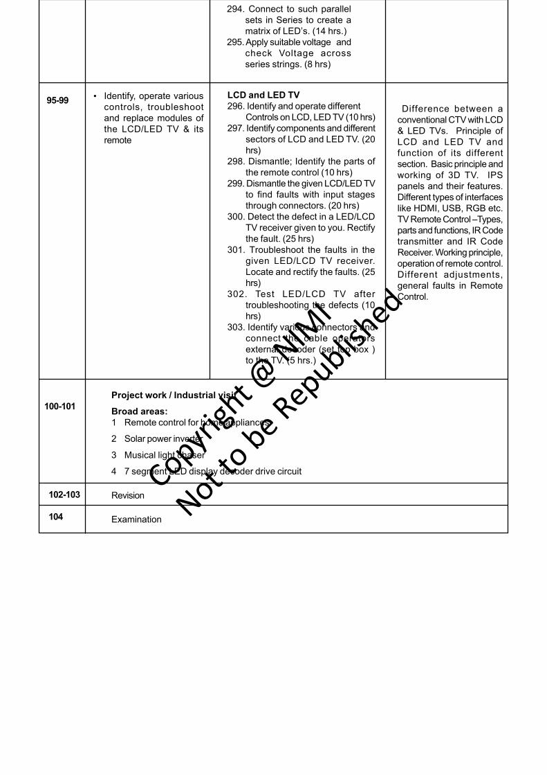
• Identify, operate variouscontrols, troubleshootand replace modules ofthe LCD/LED TV & itsremote
95-99 LCD and LED TV296. Identify and operate different
Controls on LCD, LED TV (10 hrs)297. Identify components and different
sectors of LCD and LED TV. (20hrs)
298. Dismantle; Identify the parts ofthe remote control (10 hrs)
299. Dismantle the given LCD/LED TVto find faults with input stagesthrough connectors. (20 hrs)
300. Detect the defect in a LED/LCDTV receiver given to you. Rectifythe fault. (25 hrs)
301. Troubleshoot the faults in thegiven LED/LCD TV receiver.Locate and rectify the faults. (25hrs)
302. Test LED/LCD TV aftertroubleshooting the defects (10hrs)
303. Identify various connectors andconnect the cable operatorsexternal decoder (set top box )to the TV. (5 hrs.)
Difference between aconventional CTV with LCD& LED TVs. Principle ofLCD and LED TV andfunction of its differentsection. Basic principle andworking of 3D TV. IPSpanels and their features.Different types of interfaceslike HDMI, USB, RGB etc.TV Remote Control –Types,parts and functions, IR Codetransmitter and IR CodeReceiver. Working principle,operation of remote control.Different adjustments,general faults in RemoteControl.
100-101Project work / Industrial visitBroad areas:1 Remote control for home appliances
2 Solar power inverter
3 Musical light chaser
4 7 segment LED display decoder drive circuit
Revision
Examination
102-103
104
Copyrigh
t @ NIM
I
Not to be Republish
ed

1
Electronics & Hardware Sector Related Theory for Exercise 4.1.243-248Electronic Mechanic - Fiber Optic Communication
Fiber optic communicationObjectives : At the end of this lesson you shall be able to• define the fiber optic communication• explain the block diagram and function of the fiber optic communication• describe the different basic elements of the OFC system• explain the working principle of each element• state the advantages and disadvantages of the optical fiber communication• state the applications of the fiber optic communication.
Fiber optics is a branch of optics that deals with the studyof propagation of light through transparent dielectricwave guides.
Fiber-optic communication is a method of transmittinginformation from one place to another by sending pulsesof light through an optical fiber.
A simple typical optical fiber telecommunication systemis as shown in Fig 1.
When the input data in the form of electrical signals, isgiven to the transmitter circuitry; it converts them into lightsignal with the help of a light source. This source is of LEDwhose amplitude, frequency and phases must remainstable and free from fluctuations in order to have efficienttransmission. The light beam from the source is carriedby a fiber optic cable to the destination circuitry whereinthe information is transformed or converted back to theelectrical signal by a receiver circuit.
The Receiver circuit consists of a photo detector alongwith an appropriate electronic circuit, which is capable ofmeasuring magnitude, frequency and phase of the opticfield. This type of communication uses the wave lengthsnear to the infrared band that are just above the visiblerange. Both LED and Laser can be used as light sourcesbased on the application.
Visible light range
Light is an electromagnetic signal like radio wave. It canbe modulated by the information signal and sent over thefiber- optic cable. The frequency of light is extremelyhigh; it can be used to accommodate very wide bandwidthof the information and extremely high data rates can beachieved with excellent reliability. Fig 3 shows thefrequency spectrum and wavelengths of visible lightspectrum.
Fiber-optics have revolutionized the telecommunicationindustry and have played a major role in this. Because ofits advantages over electrical signal transmission, opticalfibers have largely replaced copper wire communicationsin core networks in the developed world. Optical fiber isused by many telecommunication companies to transmittelephone signals, Internet communication, and cabletelevision signals.
A detailed block diagram of optical fiber communicationsystem is shown in Fig 2.
Basic elements of a fiber optic communication system
There are three main basic elements of fiber opticcommunication system. They are
1 Compact light source
2 Low loss optical fiber
3 Photo detector
Copyrigh
t @ NIM
I
Not to be Republish
ed

2
These materials include silicon, germanium, InGaAs,etc.
Advantages
The primary advantages of the Fiber-optic cables overconventional cables and radio waves are:
1 Wider band width
Optical fiber have greater information capacity thanmetallic cable because of the inherently wider bandwidthupto several thousand GHz available with opticalfrequencies. It has higher information carrying capacity.
2 Lower loss
With fiber-optic cables, there is less signal attenuationover long distances.
3 Small size and Light weight
Optical fibers are very small diameter in the range from10 micrometers to 50 micrometers. The space occupiedby the fiber cable is negligibly small as compared to theconventional electrical copper cables.
4 Security
Fiber-optic cables cannot be "tapped" as easily aselectrical cables.
5 Environmental immunity
OFC cables are more resistant to environment extremesincluding weather variations than metallic cables. Opticcables also operate over a wide temperature range andare less affected by corrosive liquids and gases.
6 Electrical Isolation
Optical -fibers are fabricated from glass or plasticpolymers, they are electrical insulators therefore they donot exhibit earth loop, interference problems,electromagnetic waves or any high current lightning.
7 Potential low cost and maintenance
In comparison with the copper conductors optic-fiberoffers low cost line communication. This is becausemany miles of optical cables are easier and less expensiveto install than the same amount of copper wire or cable.
Disadvantages
The cost of interfacing equipments necessary to convertelectrical signals to optical signals is more. (Opticaltransmitters, receivers). Splicing fiber optic cable is alsomore difficult.
1 Expensive over short distance.
2 Requires highly skilled installers.
3 Adding additional nodes is difficult.
Ruggedness
The main disadvantage of the fiber-optic cable is its smallsize and brittleness makes more difficult to work with it.
Fiber-Optic Applications
Telecommunication applications are widespread, rangingfrom global networks to desktop computers. This involves
Accessories like connectors, switches, OFC couplers,multiplexing devices, amplifiers and splicer are alsoessential elements in this optical fiber communicationsystem.
1 Compact light source
Depending on the applications , the light sourcerequirements may vary. The requirements of the sourcesincluding power, speed, spectral line width, noise,ruggedness, cost, temperature, and so on. Twocomponents are used as light sources: light emittingdiodes (LEDs) and laser diodes.
The light emitting diodes are used for short distances andlow data rate applications due to their low bandwidth andpower capabilities. Two such LEDs structures includeSurface and Edge Emitting Systems. The surface emittingdiodes are simple in design and are reliable, but due to itsbroader line width and modulation frequency limitation,edge emitting diodes are mostly used. Edge emittingdiodes have high power and narrower line widthcapabilities.
For longer distances and high data rate transmission,Laser Diodes are preferred due to its high power, highspeed and narrower spectral line width characteristics.But these are inherently non-linear and more sensitive totemperature variations.
2 Low loss optical fiber
The purpose of optical fiber is to transmit light signal fromtransmitter to receiver. Optical fiber is a cable, which isalso known as cylindrical dielectric waveguide made oflow loss material. An optical fiber considers the parameterslike the environment in which it is operating, the tensilestrength, durability and rigidity. The fiber optic cable ismade of high quality extruded glass (si) or plastic, and itis flexible. The diameter of the fiber optic cable is inbetween 0.25 to 0.5mm (slightly thicker than a humanhair).
3 Photo detectors
The purpose of photo detectors is to convert the lightsignal back to an electrical signal. Two types of photodetectors are mainly used for optical receiver in opticalcommunication system: PN photo diode and avalanchephoto diode. Depending on the applications wavelengths,the material composition of these devices may vary.
E& H : Electronic Mechanic (NSQF LEVEL - 5) - Related Theory for Ex 4.1.243 - 248
Copyrigh
t @ NIM
I
Not to be Republish
ed

3
the transmission of voice, data, or video over distancesof less than a meter to hundreds of kilometers using fiberdesigns.
Optical fiber is used extensively for transmission of data.Multinational firms need secure, reliable systems totransfer data and financial information between buildingsto the desktop terminals or computers and to transferdata around the world. Cable television companies alsouse optical fiber communication system for the deliveryof digital video and data services. The high bandwidthprovided by fiber makes it perfect choice for transmittingbroadband signals, such as high-definition television(HDTV) telecasts.
Intelligent transportation systems, such as smart highwayswith intelligent traffic lights, automated tollbooths, andchangeable message signs, also use fiber-optic-basedtelemetry systems.
Another important application for optical fiber is thebiomedical industry. Fiber-optic systems are used inmost modern telemedicine devices for transmission ofdigital diagnostic images. Other applications for opticalfiber include space, military, automotive, and the industrialsector.
Optical fiberObjectives : At the end of this lesson you shall be able to• define optical cable• explain the construction details of an optical cable• define refractive index and total internal deflection• explain the working principle of an optical cable• state the types of fiber• differentiate the single mode and multi mode optical cable.
What is an optical fiber?
Typically, fiber optics are long, thin strands of glass(SiO2) about the diameter of human hair; some can bemade out of plastic. Long distance telecommunicationsystems always use glass because of its lower opticalabsorption during transmission to maintain the signalstrength. When arranged in bundles, they are calledoptical cables which are used to transmit light signalscontaining information over long distances.
Construction of optical fiber
The structure of optical fiber is shown in Fig 1.
Core
The core of a fiber cable is a cylinder of plastic or silica orglass that runs all along the fiber cable's length, andoffers protection by cladding. The diameter of the coredepends on the application used. Due to internalreflection, the light travelling within the core reflects fromthe core and the cladding boundary. The core crosssection needs to be a circular one for most of theapplications.
Cladding
Cladding is an outer optical material that protects thecore. The main function of the cladding is that it reflectsthe light back into the core. When light enters through thecore (dense material) into the cladding(less densematerial), it changes its angle, and then reflects back tothe core.
Buffer jacket
The main function of the buffer is to protect the fiber fromdamage while arranged in optical cables. These bundlesare protected by the cable's strength members covering.
Outer jacket
Fiber optic cable's jackets are available in different coloursthat can easily make us recognize the exact colour of thecable we are dealing with. The colour yellow clearlysignifies a single mode cable, and orange colour indicatesmultimode. It is also given mechanical strength to theoptical cables.
Characteristics of light
Reflection: The bouncing back of rays of light from apolished and shiny surface is called reflection of light.
Refraction: It is the bending of light ray that occurs whenthe light ray passes from one medium to the other.
1 Core
2 Cladding
3 Buffer
4 Jacket
E& H : Electronic Mechanic (NSQF LEVEL - 5) - Related Theory for Ex 4.1.243 - 248
Copyrigh
t @ NIM
I
Not to be Republish
ed

4
Angle of incidence: The angle at which light strikes asurface with respect to the normal.
Angle of reflection: The angle at which light is reflectedfrom a surface.
Index of refraction
The index of refraction (or refractive index) is a way ofmeasuring the speed of light in a material. Light travelsfastest in vacuum, such as in outer space. The speed oflight in a vacuum is about 300,000 kilometers (186,000miles) per second. The refractive index is the ratio of thespeed of light in vacuum to the speed of light in thatmedium. The refractive index of a vacuum is therefore 1,by definition.
Total internal reflection
The heart of an optical communication system is theoptical fiber that acts as the transmission channel carryingthe light beam loaded with information.
When the light ray strikes the interface at an anglegreater than the critical angle, the light ray does not passthrough the interface into the glass. The effect is as if amirror existed at the interface.
When this occurs the angle of reflection is equal to theangle of incident as if a real mirror were used. This actionis known as total internal reflection.
Critical angle is the angle of incidents that causes therefracted light to travel along the interface between twodifferent media. If the angle of incidents is made greaterthan the critical angle, the reflection occurs instead ofrefraction.
Working principle of fiber optic cable
The principle of operation of an optical fiber lies in thebehaviour of light as shown in Fig 3 that the light alwaystravels in straight line and at constant speed. In this, thelight propagates in straight lines, but it is reflected insidethe optical Fiber. Million and trillion times of reflected bythe clad, it acquires the shape of the optical fiber. Soeffectively, it is said to have been travelling along theFiber as shown in the Fig 3. It changes its direction onlyif there is a change in the dielectric medium . Thepropagation of light within an optical fiber is necessary totake in to account the refractive index of the dielectricmedium.
Refractive index of a medium is defined as the ratio ofvelocity of light in vacuum to velocity of light in medium.
Refractive index = medium in light ofVelocity vacuum in light ofVelocity
Since, the velocity of light in any solid, transparentmaterial is less than in vacuum, the refractive index ofsuch material is always greater than 1. A ray of lighttravels slowly in an optical medium than one that is lessdense. Now, the direction that the light approaches theboundary between the two materials is very important.When a ray is incident on the interface between twodielectrics of differing refractive indices, refraction occurs.The light is refracted and also partly reflected internally inthe same medium; which is referred as Partial InternalReflection.
Classification of optical fiber
There are two basic ways of classifying fiber
1 Based on the modes
i Single mode fiber
ii Multi mode fiber
2 Based on index of refraction varies across the crosssection of the cable.
i Step index fiber
ii Graded index fiber
Single mode fibers
The single mode optical fiber SMF (mono mode opticalfiber, single mode optical waveguide, or uni mode fiber)type has the smaller core diameter in the order of3.5 x 10-4 inches or 9 microns and a cladding diameter of125 mm. These fibers are used in telephone and televisiondue to small cores.
E& H : Electronic Mechanic (NSQF LEVEL - 5) - Related Theory for Ex 4.1.243 - 248
Copyrigh
t @ NIM
I
Not to be Republish
ed

5
This SMF is designed to carry only a single ray of light(mode). Although the ray travels parallel to the length ofthe fiber, it is often called transverse mode since itselectromagnetic vibrations occur perpendicular(transverse) to the length of the fiber.
Multi mode fibers
The MMF type has larger core diameters on the order of2.5 x 10-3 inches or 62.5 microns as to transmit manysignals per fiber. While the number of light reflectionsincreased as the light passes through the core increases.It creates the ability for more data to pass through at agiven time. Because of the high dispersion and attenuationrate with this type of fiber, the quality of the signal isreduced over long distances. This application is typicallyused for short distance, data and audio/video applicationsin LANs. RF broadband signals commonly used by thecable companies, cannot be transmitted over multimodefiber.
Difference between Single Mode & Multi Mode
Index profile of the optical fiber
Index profile of an optical fiber is the refractive indexdistribution across the core and the cladding of the fiber.
Small core(9 microns) Larger core than single-mode cable (50 micronsor greater)
Less dispersion Allows greater dispersionand therefore, loss ofsignal.
Suited for long-distance Used for long-distance applications (upto-3 km) application, but shorter
than single-mode(upto2 km)
Used lasers as the light Uses LEDs as the source for distances of light source oftenseveral thousand meters within LANs or distances
of a couple of hundredmeters.
There are two basic ways
Step index fiber
It has an index of refraction profile that "steps" from low-to-high-to-low as measured from cladding -to-core-to-cladding. Due to its larger core, some of the light rays thatmay travel a direct route, whereas others zigzag as theybounce off the cladding. These alternate paths cause thedifferent groups of light rays, referred to as modes, toarrive separately at the receiving point. The light raysbegins to spread out, losing its well-defined shape. Theneed to leave spacing between pulses to preventoverlapping limits the amount of information that can besent. This type of fiber is best suited for transmission overshort distances.
Graded index fiber
In which refractive index reduces gradually (smoothly andcontinuously) as a function of radial distance from thefiber centre. The index of refraction decreases in proportionto the distance away from the center of the fiber core. Thehigher refractive index at the center makes the light raysmoving down the axis advance more slowly than thosenear the cladding. Due to the graded index, light in thecore curves helically rather than zigzag off the cladding,reducing its travel distance. The shortened path and thehigher speed allow light at the periphery to arrive at areceiver at about the same time as the slow but straightrays in the core axis. This results digital pulse suffers lessdispersion. This type of fiber is best suited for local-areanetworks.
Specifications
Information Services and Technology (IST) currentlyspecifies the installation of 62.5/125 micron multimodeand 8.3/125 micron single mode fiber optic cable tosupport data communication services.
The following IST specifications for the selection andinstallation of fiber-optic cable and associated hardwareare intended to ensure a reliable and consistent fiber opticmedia infrastructure
E& H : Electronic Mechanic (NSQF LEVEL - 5) - Related Theory for Ex 4.1.243 - 248
Copyrigh
t @ NIM
I
Not to be Republish
ed

6
1 Single mode fibers
i Thickness of fiber: 8.3 to 125micro meter
ii Wave length (to be used): 1310 nano meter,1550nano meter
iii Maximum attenuation: 1.0dB/ kilometer
iv Capable to support tensile load of 180 Kg
v Capable of minimum crush resistance of 152 Kg/cm
vi Cable should be tight buffered, ie., the fiber should notbe placed loosely in cladding layer.
2 Multi mode fiber
i Thickness of fiber: 8.3 to 125 micrometer.
ii Wave length (to be used): 850 nano meter,1550 nanometer.
iii Capable to support tensile load of 180 Kg.
iv Capable of minimum crush resistance of 152 Kg/cm.
v Folded core ie., fibers with cladding layer should havebeen closely bunched together.
Losses in optical fibersObjectives : At the end of this lesson you shall be able to• state the types of losses in the fiber optics• explain the attenuation losses in an optical cable• define dispersion• state the types of dispersion and explain about each type.
Losses
The Signal transmitting through the fiber is degraded bytwo mechanisms. (Fig 1)
1 Attenuation
2 Dispersion
Both are important to determine the transmissioncharacteristics of the fiber at operating wavelength.
Attenuation
Power loss in a fiber cable is probably the most importantcharacteristics of the cable. Power loss is often called asattenuation.
Attenuation is a measure of decay of signal strength orloss of light power that occurs as light pulses propogatethrough the length of the fiber.
Attenuation has several adverse effects on performance,including reducing the system bandwidth, informationtransmission rate, efficiency, and overall system capacity.
Total power loss in an optical fiber cable is
A(dB) = 10 log (Pout/Pin)
Where
A(dB) - Total reduction in power level, attenuation.
Pout - Cable output power (watts) and
Pin - Cable input power (watts)
The basic attenuation mechanisms in a fiber are
1 Absorption
2 Scattering and
3 Radiative losses of the optical energy
Absorption is related to the fiber material and scatteringalso due to the fiber material and with structuralimperfections in the optical waveguide.
Radiative losses occur whenever an optical fiber undergoes a bend (both microscopic and macroscopic) of finiteradius of curvature as shown in Fig 2.
Dispersion
Dispersion means the spreading of light pulse as itpropagates through the fiber as shown in Fig 3.
It introduces Intersymbol interference (ISI). It limits theinformation carrying capacity of fiber.
E& H : Electronic Mechanic (NSQF LEVEL - 5) - Related Theory for Ex 4.1.243 - 248
Copyrigh
t @ NIM
I
Not to be Republish
ed

7
The dispersion effect can be explained on the basis ofbehaviour of group velocities of the guided modes in theoptical fiber. Group velocity means the velocity at whichenergy in a pulse travel along the fiber.
Types of dispersion
Dispertion is mainly 2 types
1 Intramodal dispersion
2 Intermodal dispersion
Intramodal dispersion is divided into
i Material or chromatic dispersion
ii Waveguide dispersion
iii Group velocity dispersion (GVD) or Modal dispersion
Intramodal dispersion
Intramodal dispersion is pulse spreading that occurswithin a single mode.
It arises due to group velocity being a function ofwavelength. The increasing spectral width of the opticalsource will increase the intramodal dispersion.
Material dispersion (or) Chromatic dispersion
1 This dispersion arises due to the variation of therefractive index of the core material as a function ofwavelength or frequency of light.
2 To minimize the material dispersion choosing sourceswith narrower spectral output width, or by operating atlonger wavelengths.
Waveguide dispersion
1 Waveguide dispersion occurs when a single-modefiber only confines about 80% on the optical power tothe core.
2 The amount of waveguide dispersion depends on thefiber design.
Group velocity dispersion
1 Group velocity is the velocity at which the energy in aparticular mode travels along the fiber, or it is thevelocity of a group of wave length.
2 This type pulse spreading occurs when each modehaving different value of the group velocity at singlefrequency.
Intermodal distortion (or) Multimode dispersion
1 The intermodal distortion arises due to the variation inthe group delay for each individual mode at singlefrequency.
2 This distortion is available in multimode fibers.
Encoding and decoding of lightObjectives : At the end of this lesson you shall be able to• define encoding and decoding of light• explain the different types of optical sources• state the requirements of light sources in the fiber optical communication system• explain the principle of operation of LASER diode and different types of optical decoders• state the requirement of photo detectors used in the optical communication system.
Encoding in optical fiber transmission means thetransmission of analog optical information through fiberoptics digitally as shown in Fig 1.
This improves the acceptable signal-to-noise ratio (SNR)by 20 to 30 dB over analog transmission.
Transmitter
Fiber optic transmitters are typically composed of abuffer, driver and optical source. The buffer provide bothan electrical connection and isolation between thetransmitter and the electrical system supplying the data.The driver provides electrical cover to the optical source.Finally the optical source converts the electrical currentto the light energy with the same pattern.
Optical source
Optical Sources are active components whosefundamental function is to convert the electrical energyinto optical energy(light) in an effective manner. Hencethe optical sources are transducers.
E& H : Electronic Mechanic (NSQF LEVEL - 5) - Related Theory for Ex 4.1.243 - 248
Copyrigh
t @ NIM
I
Not to be Republish
ed

8
Optical source is major component in an opticaltransmitter.
Popularly used optical sources are Light emitting diode(LED) and semiconductor laser diodes (also referred toas injection laser diodes or ILDs).
Requirements of light sources for communication
i Light output should be highly directional.
ii It must require very small power for its operation.
iii Optical output should be stable irrespective of changesin temperature.
iv The light source should have compact size and highefficiency.
v High optical output power and coupling efficiency.
vi It is essential that the source is comparatively cheapand highly reliable in order to compete withconventional transmission techniques.
Almost all these requirements are satisfied by LASERand LED. Both operate in forward-biased mode.
1 LED-Monochromatic incoherent source.
2 LASER-Monochromatic coherent source.
Light Emitting Diode (LED)
LEDs are used in optical communication systems thatrequire bit rate less than approximately 100-200 mbps.Itis mostly coupled with multimode fiber.
It covers broad spectrum of wavelengths and the emittedpower is proportional to the diode current.
LASER diode
LASER is acronym for Light Amplification by StimulatedEmission of Radiation.
Emission of light from LED
Conduction band of the semiconductor is populated byelectrons injected into it. By the forward current throughthe junction and light is generated when these electronsrecombine with holes in valence band to emit a photon.
LED can be used in fiber transmission applications musthave
i High Radiance output or brightness.
ii Fast transmission response time.
iii High quantum efficiency.
Ideal LASER light is single-wavelength only. This isrelated to the molecular characteristics of the materialbeing used in the LASER. It is formed in parallel beamsand in single phase. That is, it is coherent.
Laser diode is available in two different packages asshown in Fig 4.
1 Can type package
2 Frame type package
The lasing medium can be a gas, a liquid, an insulatingcrystal, or a semiconductor.
Principle of operation
The three different mechanisms are shown in Fig 5below.
1 Absorption: An atom in a lower level absorbs aphoton and moves to an upper level.
2 Spontaneous emission: An atom in an upper levelcan decay spontaneously to the lower level and emita photon if the transition between upper and lowerenergy level. This photon has a random direction andphase.
3 Stimulated emission: An incident photon causes anupper level atom to decay and emitting a "stimulated"photon whose properties are identical to those of theincident photon. The term "stimulated" underlines thefact that this kind of radiation only occurs if an incidentphoton is present. The amplification arises due to thesimilarities between the incident and emitted photons.
E& H : Electronic Mechanic (NSQF LEVEL - 5) - Related Theory for Ex 4.1.243 - 248
Copyrigh
t @ NIM
I
Not to be Republish
ed

9
Comparison of LASER & LED
The differences between LASER and LED for various parameters are listed in the TABLE below.
Sl. No. Parameter LASER LED
1. Output beam Coherent Incoherent
2. Coupling co efficiency High Low
3. Output power High Low
4. Cost Expensive Less
5. Application Moderate Long distancedistance with with high data ratelow data rate
6. Circuit complexity Complex Simple
7. Temperature dependent More Less
Optical receiver
Optical receiver (photo detector) converts the variation inoptical power into a corresponding variation in the electriccurrent. The design of an optical receiver is much morecomplicated than that of an optical transmitter becausethe receiver must first detect weak, distorted signals andthen make decisions on what type of data was sent basedon an amplified version of this distorted signal.
The optical receiver can be broken down into three parts.These consist of:
1 Channel coupler (Output)
2 Detector
3 Signal processor
Channel coupler (Output)
In a fiber system, the output coupler merely directs thelight emerging from the fiber into the light detector. Thislight is radiated in a pattern identical to the fiber'sacceptance cone as shown in Fig 6.
Detector
The detector is an essential component of an optical fibercommunication system and is one of the crucial elementswhich decides the overall system performance.
The information being transmitted must now be taken offthe carrier wave. In the fiber system, the optic wave isconverted into an electric current by a photo detector.
E& H : Electronic Mechanic (NSQF LEVEL - 5) - Related Theory for Ex 4.1.243 - 248
Copyrigh
t @ NIM
I
Not to be Republish
ed

10
Signal processor
For analog transmission, the signal processor includesamplification and filtering of the signal.
In addition to filtering of the constant bias, any otherundesired frequencies should be blocked from furthertravel.
An ideal filter passes all frequencies contained in thetransmission information and rejects all the others. Thisimproves the clarity of the intended transmission. Properfiltering maximises the signal to noise ratio.
Requirements of photo detectors
1 High sensitivity at operating wavelength
2 High fidelity: To reproduce the received signalwaveform with fidelity, for analog transmission theresponse of the photo-detector must be linear withregard to the optical signal over a wide range.
3 High quantum efficiency
4 Short response time to obtain suitable bandwidth
5 A minimum noise introduced by the detector.
6 Small size
7 Stable performance
8 High reliability
9 Low bias voltage
10 Low cost
The two types of photodiodes used are the P-I-N photo-detector and the avalanche photo diode(APD).
P-I-N Photodetector
The circuit symbol of P-I-N diode is shown in Fig 7 below.
1 The pin photo detector structure consists of p and nregions separated by a very lightly doped intrinsicregion.
2 When the photodiode is reverse biased, the intrinsicregion of diode is fully depleted of carriers.
Avalanche Photo Diode (APD)
The circuit symbol of the avalanche photo diode is shownin Fig 8.
1 Avalanche photo diodes internally multiply the primarysignal photo current before it enters the input circuitryof the following amplifier.
2 It has high internal gain and its responsivity is betterthan the pin photo diode.
3 Extremely high electric field region is created. Most ofthe photons are absorbed in the depletion region andthe primary electron-hole pairs are generated.
Comparison of PIN diode and APD
The differences between the PIN diode and the Avalanche Photo Diode for various parameters are given below:
Sl. No. Parameter PIN APD
1 Sensitivity Less Sensitivity More sensitivity(0-12db) (5-15db)
2 Biasing Low reverse High reverse biased voltagebiased voltage (20-400v)(5 to 10v)
3 Wave length region 300- 1100nm 400-1000nm
4 Gain No internal Gain internal Gain
5 S N Ratio Poor Better
6 Detector circuit Simple More complex
7 Cost cheaper More expensive
E& H : Electronic Mechanic (NSQF LEVEL - 5) - Related Theory for Ex 4.1.243 - 248
Copyrigh
t @ NIM
I
Not to be Republish
ed

11
Pulse modulation techniqueObjectives : At the end of this lesson you shall be able to• define pulse• state the types of pulse modulation• explain PCM,PAM,PWM and PPM• state the advantages, disadvantage and applications of each type of modulation• compare the different types of pulse modulation techniques.
Types of modulation - Tree Diagram
AM, FM modulation & demodulation alreadywe discussed in Semester 3 CommunicationElectronics topic. Here we can discussed withPWM, PPM.
Pulse
A pulse is an abruptly changing voltage or current wavewhich may or may not repeat itself as shown in Fig 2. TheFig 2(b) Shows a repetitive pulse train and Fig 2(c) showsa pulse with its trailing and leading edges.
Pulse modulation
It may be defined as a modulation system in which someparameter of a train of pulse is varied in accordance withthe instantaneous value of the modulating signal. In thissystem, waveforms are sampled at regular intervals and
the information is transmitted through the sampling rate.The parameters of the pulses which may be varied are :amplitude, width (or duration), position and time etc
In pulse modulation, there are different types of modulationtechniques for analog and digital as given below:
PCM : Pulse Code Modulation for Digital Modulation.
PPM : Pulse Position Modulation for Analog Modulation
PWM : Pulse Width Modulation for Analog Modulation.
PAM : Pulse Amplitude Modulation for AnalogModulation.
1 Pulse Code Modulation (PCM)
PCM will transmit the analog in a digital form, whosesignal is sampled at regular intervals of time and quantizedat same quantum levels to digital code as shown in Fig 3.We know that digital code is nothing but binary codewhich consists of 1's and 0's that is logic1 and logic0. Sowe will transmit the digital data in the form of 1's and 0's.When the signal is received by the receiver, demodulatorin the receiver will demodulate the binary signal back intopulses with same quantum levels like in modulator andthese pulses are again used for regenerating the requiredanalog signal.
Advantages of Pulse Code Modulation
1 Pulse code modulation will have low noise additionand data loss is also very low.
2 The received signal is exact replica of the transmittingsignal without any distortion loss.
E& H : Electronic Mechanic (NSQF LEVEL - 5) - Related Theory for Ex 4.1.243 - 248
Copyrigh
t @ NIM
I
Not to be Republish
ed

12
3 PCM can encode the data.
4 Multiplexing of signals can also be done using pulsecode modulation. Multiplexing is nothing for addingthe different signals and transmitting the signal atsame time.
5 Pulse code modulation permits the use of pulseregeneration.
6 PCM can be used in storing data.
Disadvantages of Pulse Code Modulation
1 Specialized complicated complex circuitry is requiredfor transmitting and encoding.
2 Pulse code modulation receivers are costlier thanother modulation receivers.
3 Developing pulse code modulation is bit complicatedand checking the transmission quality is also difficultand takes more time.
4 It requires larger bandwidth than normal analog signalsto transmit message.
5 Channel bandwidth should be more for digitalencoding.
6 Decoding also needs special equipments and theyare also too complex.
Applications of Pulse Code Modulation (PCM)
i Pulse code modulation is used in telecommunicationsystems, air traffic control systems etc.
ii Pulse code modulation is used in compressing thedata that is why it is used in storing data in optical diskslike DVD, CDs etc. PCM is even used in the databasemanagement systems.
iii Pulse code modulation is used in mobile phones,normal telephones etc.
iv Remote controlled cars, planes, trains use pulse codemodulations technique.
2 Pulse Amplitude Modulation (PAM)
In pulse amplitude modulation, the amplitude of regularinterval of periodic pulses or electromagnetic pulses arevaried in proportion to the sample of modulating signal or
message signal as shown in Fig 4. This is an analog typeof modulation. These sample pulses can be transmitteddirectly using wired media or we can use a carrier signalfor transmitting through wireless. It is almost equal toamplitude modulation.
Advantages of Pulse Amplitude Modulation (PAM)
1 It is the base for all digital modulation techniques andit is simple process for both modulation anddemodulation technique.
2 No complex circuitry is required for both transmissionand reception. Transmitter and receiver circuitry issimple and easy to construct.
3 PAM can generate other pulse modulation signalsand can carry the message or information at the sametime.
Disadvantages of Pulse Amplitude Modulation (PAM)
1 Bandwidth should be large for transmitting the pulseamplitude modulation signal.
2 The frequency varies according to the modulatingsignal or message signal. Due to these variations inthe signal frequency, interferences will be there. Sonoise will be great. Pulse amplitude signal varies, sopower required for transmission will be more, peakpower is also, even at receiving more power is requiredto receive the pulse amplitude signal.
Applications of Pulse Amplitude Modulation (PAM)
i It is mainly used in Ethernet which is type of computernetwork communication.
ii It is also used for photo biology which is a study ofphotosynthesis.
iii Used as electronic driver for LED lighting.
iv Used in many micro controllers for generating thecontrol signals etc.
3 Pulse Width Modulation (PWM) or Pulse DurationModulation (PDM):
It is a type of analog modulation. In pulse width modulationor pulse duration modulation, the width of the pulsecarrier is varied in accordance with the sample values ofmodulating signal as shown in Fig 5. In this the amplitude
E& H : Electronic Mechanic (NSQF LEVEL - 5) - Related Theory for Ex 4.1.243 - 248
Copyrigh
t @ NIM
I
Not to be Republish
ed

13
is made constant and width of pulse and position of pulseis made proportional to the amplitude of the signal.
The conventional method of generating a PWM modulatedwave is to compare the message signal with a rampwaveform using a comparator. The block diagram requiredfor the generation of a simple PWM is shown in the Fig 6.
Advantages of Pulse Width Modulation (PWM)
i Noise interference is less due to amplitude has beenmade constant.
ii Signal can be separated very easily at demodulationand noise can also be separated easily.
iii Synchronization between transmitter and receiver isnot required.
Disadvantages of Pulse Width Modulation (PWM)
i Power will be variable because of varying in width ofpulse. Transmitter can handle the power even formaximum width of the pulse.
ii Bandwidth should be large to use in communication,should be huge even when compared to the pulseamplitude modulation.
Applications of Pulse Width Modulation (PWM)
i PWM is used in telecommunication systems.
ii PWM can be used to control the amount of powerdelivered to a load without incurring the losses. So,this can be used in power delivering systems.
iii Audio effects and amplifications purposes also used.
iv PWM signals are used to control the speed of therobot by controlling the motors.
v PWM is also used in robotics.
vi Embedded applications.
vii Analog and digital applications etc.
4 Pulse Position Modulation (PPM)
In the pulse position modulation, the position of eachpulse in a signal by taking the reference signal is variedaccording to the sample value of message or modulatingsignal instantaneously. In the pulse position modulation,width and amplitude is kept constant. It is a technique thatuses pulses of the same breadth and height but isdisplaced in time from some base position according tothe amplitude of the signal at the time of sampling. Theposition of the pulse is 1:1 which is proportional to thewidth of the pulse and also proportional to theinstantaneous amplitude of sampled modulating signal.The position of pulse position modulation is easy whencompared to other modulation.
The waveform of the Pulse position modulation is asfollows. (Fig 7)
The Pulse Position Modulation (PPM) is a modulationtechnique designed to achieve the goals like simpletransmitter and receiver circuitry, noise performance,constant bandwidth and the power efficiency and constanttransmitter power.
In Pulse Position Modulation the amplitude of the pulseis kept constant as in the case of the FM and PWM toavoid noise interference. Unlike the PWM the pulse widthis kept constant to achieve constant transmitter power.
Fig 8 shows the block diagram of PPM.
It requires pulse width generator and monostablemultivibrator.
E& H : Electronic Mechanic (NSQF LEVEL - 5) - Related Theory for Ex 4.1.243 - 248
Copyrigh
t @ NIM
I
Not to be Republish
ed

14
Pulse width generator is used for generating pulse widthmodulation signal which will help to trigger the monostablemultivibrator, here trialling edge of the PWM signal isused for triggering the monostable multivibrator. Aftertriggering the monostable multivibrator, PWM signal isconverted into pulse position modulation signal.
Advantages of Pulse Position Modulation (PPM):
1 Pulse position modulation has low noise interferencewhen compared to PAM because amplitude andwidth of the pulses are made constant duringmodulation.
2 Noise removal and separation is very easy in pulseposition modulation.
3 Power usage is also very low when compared to othermodulations due to constant pulse amplitude andwidth.
Disadvantages of Pulse Position Modulation (PPM):
1 The synchronization between transmitter and receiveris required, which is not possible for every time and weneed dedicated channel for it.
2 Large bandwidth is required for transmission same aspulse amplitude modulation.
3 Special equipments are required in this type ofmodulations.
Applications of Pulse Position Modulation (PPM):
1 Used in non coherent detection where a receiver doesnot need any Phase Locked Loop(PLL) for trackingthe phase of the carrier.
2 Used in radio frequency (RF) communication.
3 Also used in contactless smart card, high frequency,RFID (radio frequency ID) tags, etc.
Comparison between PAM,PWM,PPM
The differences between PAM,PWM and PPM are given in the table below:
Sl. No. PAM PWM(or PDM, PLM) PPM
1. Amplitude of the carrier The width (or duration or length) of The relative position of thepulse is proportional to the carrier pulse is proportional to carrier pulse is proportional tothe amplitude of the the amplitude of the modulating the amplitude of the modulatingmodulating signal. signal. signal.
2. The B.W. of the transmitting The B.W. of the channel depends The B.W. of the channeldependschannel depends upon the upon rise time of the pulse upon the rise time of the pulse.width of the pulse. B.W. = ½ t B.W. = ½ t
Where t is the rise time
3. The instantaneous power of The instantaneous power of The instantaneous power of thethe transmitter varies. the transmitter varies. transmitter remains constant.
4. Noise interference is high. Noise interference is low. Noise interference is low.
5. Similar to amplitude Similar to frequency modulation Similar to phase modulation(PM)modulation(AM) (AM)
1 Fiber optic cable connector
• A fiber - optic cable connector is a mechanical devicewhich is used to terminate the end of a fiber-opticcable and it enables a quicker connection anddisconnection with respect to joining which is apermanent, method of joining. The use of fiber-opticcable connectors net result is attenuation in signalstrength.
• It consists of an adapter and two connector plugs.Most of the connectors are spring loaded so that thetwo fiber faces remains pressed together, leaving noair-gap between them, when the connectors are mated.
• Separate connectors are made for glass to glassfibers and teflon to teflon fibers. Different types of fiberoptic cable connectors are shown in fig.1 is describedas follows:
a Standard connector (SC) - SC connectors use aceramic ferrule to deliver accurate alignment of theSingle Mode Fiber (SMF). The SC connector comeswith a locking tab that enables push on /Pull offoperation and it is simple, rugged and low cost. SCconnectors are in the shape of square or rectangle.
b Ferrule core connector (FC) - FC connectors arewidely used in fiber optic networks. This connectorused a threaded container and a position locatablenotch to achieve exact locating of the Single ModeFiber (SMF) in relation to the receiver and the opticalsource.
C Straight Tip (ST) connector - The ST connector’skeyboard bayonet design is similar to that of a BNC(Bayonet Nut Connector or Baynot Neill-Concelman)connector. The connector is used widely for multi-meter fiber (MMF) and singlemode fiber (SMF) fiber
E& H : Electronic Mechanic (NSQF LEVEL - 5) - Related Theory for Ex 4.1.243 - 248
Copyrigh
t @ NIM
I
Not to be Republish
ed

15
optic communication (FOC) and is extremely easy touse. The ST connector is manufactured in two versions- the ST and the ST-II. Both types are keyed andspring loaded, and use a “push-in and twist”mechanism. ST connectors are mainly designed foruse with glass, they can also be used with plasticFOC.
d SMA (Subminiature version-A) connector - Theobsolete SMA connector was the forerunner to the STconnector. This connector was eventually replacedby the ST, and later by SC connectors. SMA connectorsare mainly designed for use with glass, they can alsobe used with plastic FOC.
e Lucent connector (LC) - The LC, sometimes referredto as the little connector, is a small form factor FOCthat uses a 1.25mm ferrule.
f Plastic fiber optic cable connectos - There arerelatively fewer plastic connectors available whencompared to glass fiber. These connectors are cheaperand are primarily designed for easy application.Polished and epoxy options are generally not availablefor plastic connectors.
g Enterprise systems connection connector(ESCON) - ESCON connectors were developed byIBM for interfacing peripheral storage devices,including tape drives, to their mainframes. ESCON isa half-duplex serial interface that uses FOC.
h Fiber distributed data interface connector (FDDI)- FDDI provides data transmisson at 100 Mbps in adual ring token local area network within a 200-kilometer rang. The FDDI connector connects networkequipment to a wall plug.
i Opti-jack Connector - The opti-jack duplex connectorresembles the universal RJ-45 connector. Thepackage contains two ST type ferrules and is a ruggedplug-and-jack (female/male) connector.
j LX-5 Connector - The LX-5 provides high density,high performance and reliable connections. Thisconnector uses automatic metal shutter technology ina standardized small form factor package with a1.25mm ferrule.
k MT-RJ Connector - The single polymer ferrule duplexMT-RJ connector includes alignment. It is available infemale/male connectors, or a plug-and-jack format.
I MU Connector - MU connectors have a reducedfootprint and are new generation connectors usedmainly in dense applications. The connector is squareand employs a push-pull matching mehcanism.
m MT Connector - The MT connector is a ribbon cablethat has 12 fiber connectors. They are used for factoryterminated cable assemblies and cabling systems.
n E2000 Connector - Modern day telecommunicationnetworks increasingly make use of E2000 connectors.
E& H : Electronic Mechanic (NSQF LEVEL - 5) - Related Theory for Ex 4.1.243 - 248
Fig 1
The inclusion of an integrated spring loaded shutter isa unique feature of this connector. The E2000 is alatched push-pull locking connector. The majoradvantages of this connector are the enhanced safetyand high performance due to shutter mechanism andthe monobloc ferrule.
o Local connectos (LC) - which is in the shape ofround.
• The most widely used connector for fiber optic cableis SMA (Subminiature version-A).
Copyrigh
t @ NIM
I
Not to be Republish
ed

16
2 Precautions and safety aspects while handlingoptical cables
• Optical fibers are made of glass or plastic fiberstherefore, following safety precaution should be takeninto consideration while using them.
Micro bending: A problem that often occurs in cabling ofthe optical fiber is the twisting of the fiber core axis an amicroscopic scale within the cable form. This phenomenonknown as microbending result from small lateral forcesexerted on the fiber during the cabling process and itcauses losses due to radiation in both multimode andsingle mode fiber. Do bend the fiber more than 200% ofits core diameter.
Example:
• Diameter of bend for optical fiber 125mm will be 25mm
• Diameter of bend for optical fiber of 400mm will be80mm.
• Do not keep any heavy load or hand machine on thefiber.
• Protect the fiber from sharp edges otherwise that candamage its protection jacket and harm the claddingand core.
• Fiber should not come in contact of any abrasive oracetone etc.
• Do not throw the pieces of fibers in dustbin etc. and dokeep pieces of glass with optical fibers.
• Do not keep eatables or beverages near the ends ofoptical fibers as they have a high radiation.
E& H : Electronic Mechanic (NSQF LEVEL - 5) - Related Theory for Ex 4.1.243 - 248
Fiber optical splicingObjectives : At the end of this lesson you shall be able to• define splicing• state the related tools used along with splicer• explain cleaving• explain various steps involved in the splicing.
Introduction
Splicing is the process of joining two ends of optical fiberusing electric arc or mechanical means.
In practice, to cover larger distance and as well as torepair the OFC cuts, joints have to be made i.e. OFC hasto be joined. This joining is called as splicing.
Fiber splicing is a complicated procedure and requiresskilled manpower to achieve. We should completelyclean off the gel component when the cable end isstripped for termination.
The necessary tools and accessories for splicing aresplicing machine, cleaver, cable cutter, iso-propyl alcoholand tissue paper as shown in Fig 1 and 2.
Fig 1
Splicing machine
A special machine which is used to join the fiber usingfusion technique.
Clever (diamond cutter)
It is used to cut optical fiber perpendicular to cable axisexactly by 90 degrees.
Multi purpose cutter (stripper)
It is used to remove primary coating of fiber.
Iso-propyl alcohol, acetone and tissue paper
It is used to clean the dust of fiber before splicing.
Stripper ISO propyl alcohol
CleverFig 2
Copyrigh
t @ NIM
I
Not to be Republish
ed

17E& H : Electronic Mechanic (NSQF LEVEL - 5) - Related Theory for Ex 4.1.243 - 248
Fusion splicing
The fusion splicers are shown in the Fig 3.
Splicing is the practice of joining two fibers togetherwithout using fiber connectors as shown in Fig 4. Two
Fig 3 Fusion splicer Fusion optic cleaver Heat shrink tube
types of fiber splices exist: fusion splicing and mechanicalsplicing. Splicing may be made during installation orrepair.
Splices generally have lower loss and better mechanicalintegrity than connectors, while connectors make systemconfiguration much more flexible. So typically, splicesare used to connect fiber cables in outdoor applicationsand connectors terminate fiber cables inside buildings.
Fusion splicing process has to use high temperature heatgenerated by electric arc and fuse two glass fiberstogether (end to end with fiber core aligned precisely).The tips of two fibers are butted together and heated sothey melt together. This is normally done with a fusionsplicer, which mechanically aligns the two fiber ends,then applies a spark across the fiber tips to fuse themtogether.
Four basic steps to complete a proper fusion splicing
Step 1
Fig 5
Preparing the fiber - Strip the protective coatings,jackets, tubes, strength members, etc. leaving only thebare fiber showing. The main concern here is cleanliness.(Fig 5)
Step 2
Cleave the fiber - Using a good fiber cleaver, that isessential for a successful fusion splicing. The cleavedend must be mirror-smooth and perpendicular to the fiberaxis to obtain a proper splice. These cleavers canconsistently producing a cleave angle of 0.5 degree orless.(Fig 6)
Step 3
Fuse the fiber - There are two steps within this step,alignment and heating. Alignment can be manual orautomatic depending on what equipment you have. Thehigher priced equipment you use, the more accurate thealignment becomes. Once properly aligned the fusionsplicer unit then uses an electrical arc to melt both thefiber ends joined together permanently as shown in Fig7.
Step 4
Protect the fiber - Protecting the fiber from bending andtensile forces will ensure the splice not break duringnormal handling. A typical fusion splice has a tensilestrength between 0.5 and 1.5 lbs and will not break duringnormal handling but it still requires protection fromexcessive bending and pulling forces. Using heat shrinktubing, silicone gel and/or mechanical crimp protectorswill keep the splice protected from outside elements andbreakage.
Mechanical splicing method
Mechanical splicing is an optical junction where the fibersare precisely aligned and held in place by a self-contained assembly, not a permanent bond. This methodaligns the two fiber ends to a common centerline, aligning
Copyrigh
t @ NIM
I
Not to be Republish
ed

18
their cores so the lights can pass from one fiber toanother. (Fig 8)
E& H : Electronic Mechanic (NSQF LEVEL - 5) - Related Theory for Ex 4.1.243 - 248
Four steps to performing a mechanical splicing
Step 1
Preparing the fiber - strip the protective coatings, jackets,tubes, strength members, etc. leaving only the bare fibershowing. The main concern here is cleanliness.
Step 2
Cleave the fiber - The process is identical to the cleavingfor fusion splicing but the cleaving precision is not acritical aspect.
Step 3
Mechanically join the fibers - There is no heat used inthis method. Simply position the fiber ends togetherinside the mechanical splice unit. The index matchinggel inside the mechanical splice apparatus will helpcouple the light from one fiber end to the other. Olderapparatus will have an epoxy rather than the indexmatching gel holding the cores together.
Copyrigh
t @ NIM
I
Not to be Republish
ed

19
Step 4
Protect the fiber - the completed mechanical splicingprovides its own protection for the splice.
Mechanical splicing Vs Fusion splicing
Mechanical splicing
Mechanical splices are simply alignment devices,designed to hold the two fiber ends in a precisely alignedposition thus enabling light to pass from one fiber into theother. (Typical loss : 0.3 dB)
Fusion splicing
In fusion splicing a machine is used to precisely align thetwo fiber ends then the glass ends are "fused" or "welded"together using some type of heat or electric arc. Thisproduces a continuous connection between the fibersenabling very low loss transmission. (typical loss : 0.1dB)
Which method is better?
The typical reason for choosing one method over theother is economy. Mechanical splicing has a low initialinvestment but costs more per splice. While the cost persplice for fusing splicing is lower, the initial investment ismuch higher. The more precise you need the alignment(better alignment results in lower loss) the more you payfor the machine.
Precautions to be taken while laying of cable
1 Before laying the different cable sections, all reelsshould be visually inspected for possible transportationdamage.
2 Before pulling the cable, ensure the stability of thepay-off.
3 To avoid possible damage from a sudden stop, thepay-off must be equipped with a progressive brakingsystem. Under no circumstances should the reel bestopped by hand.
4 The route defined by the design should be accessibleand available in accordance with the installationschedule. The users should be advised of all proposeddeviations.
5 The installer should establish that the environmentalconditions within the routes and the installationmethods to be used are suitable for the optical fibrecable to be installed (Check the datasheet of the cableused). If the route contains sections where the opticalcable is subject to high temperatures the necessaryprotection should be provided. Look out for heatingtubes, which are not heated all the time.
E& H : Electronic Mechanic (NSQF LEVEL - 5) - Related Theory for Ex 4.1.243 - 248
6 Any measure necessary should be taken to preventthe optical cable experiencing direct stress followinginstallation.
7 The installer should determine the locations at whichreels are to be positioned during the installationprogram.
8 Where necessary, the minimum quantity of ceilingtiles, floor covers should be removed.
9 The installer should ensure that all necessary guards,protective structures and warning signs are used toprotect both the optical cable and third parties.Relevant national legislation for safe working practicesmust be complied with.
Fiber Optic Installation Safety Rules:
1 Keep all food and beverages out of the work area. Iffiber particles are ingested they can cause internalhemorrhaging.
2 Wear disposable aprons to minimize fiber particles onyour clothing. Fiber particles on your clothing can laterget into food, drinks, and/or be ingested by othermeans.
3 Always wear safety glasses with side shields andprotective gloves. Treat fiber optic splinters the sarneas you would glass splinters.
4 Never look directly into the end of fiber cables until youare positive that there is no light source at the otherend. Use a fiber optic power meter to make certain thefiber is dark. When using an optical tracer or continuitychecker, look at the fiber from an angle at least 6inches away from your eye to determine if the visiblelight is present.
5 Only work in well ventilated areas.
6 Contact lens wearers must not handle their lensesuntil they have thoroughly washed their hands.
7 Do not touch your eyes while working with fiber opticsystems until they have been thoroughly washed.
8 Keep all combustible materials safely away from thecuring ovens.
9 Put all cut fiber pieces in a safe place.
10 Thoroughly clean the work area.
11 Do not smoke while working with fiber optic systems.
Copyrigh
t @ NIM
I
Not to be Republish
ed

20
Practically every measurement in fiber optics refers tooptical power. The power output of a transmitter or theinput to receiver are "absolute" optical powermeasurements, that is, it can measure the actual value of
Fig 1
Fiber testing
After the installation of cable, next step is testing. Testingis the process to evaluate the performance of fiber opticcomponents (like fiber, connectors, splices, LED or lasersources, detectors and receivers), cable plants andsystems. Testing confirms their performance,specifications and helps understand how they will worktogether.
Procedures are required under the testing some arelisted below
1 Selection of tools
i Source and power meter, optical loss test set ortest kit with proper equipment adapters for thecable network are required for testing.
ii Reference test cables that match the cables to betested and mating adapters, including hybrids ifneeded.
iii Fiber tracer or Visual fault locator.
iv Cleaning materials - lint free cleaning wipes andpure alcohol.
v OTDR and launch cable for outside plant jobs.
2 Documentation
This is an important part of the testing of fiber. Makesure all cable layouts are available before testing thenetwork. Prepare a spread sheet of all the cables andprint a copy for recording each test data.
3 Safety notes
Fiber optic sources, including test equipment, aregenerally too low in power to cause any eye damage,but it's still a good idea to check connectors with apower meter before looking into it. Some systems likeCATV have very high power and they could beharmful.
Types of testing
There are three basic tests
1 Visual inspection for continuity or connector checking
2 Loss testing
3 Network Testing.
Visual inspection
Visual tracing
Continuity checking makes sure that the fibers are notbroken and to trace a path of a fiber from one end toanother through many connections by using a visiblelight "fiber optic tracer" or "pocket visual fault locator". It
E& H : Electronic Mechanic (NSQF LEVEL - 5) - Related Theory for Ex 4.1.243 - 248
Testing of optical fiberObjectives : At the end of this lesson you shall be able to• define testing• state the different procedures followed for testing• explain different types of testing of fiber optic component• explain the working of OTDR.
looks like a flashlight or a pen-like instrument with a lightbulb or LED source that mates to a fiber optic connector.Attach a cable to test to the visual tracer and look at theother end to see the light transmitted through the core ofthe fiber. If there is no light at the end, go back tointermediate connections to find the faulty section of thecable.
Visual fault location
A higher power version of the tracer uses a laser that canalso find faults. The red laser light is powerful enough toshow breaks in fibers or high loss connectors. It also usethis gadget to optimize mechanical splices or pre polished-splice type fiber optic connectors.
Visual connector inspection
Fiber optic microscopes are used to inspect connectorsto check the quality of the termination procedure anddiagnose problems. A well made connector will have asmooth, polished, scratch free finish and the fiber will notshow any signs of cracks, chips or areas where the fiberis either extended from the end of the ferrule( connector)or pulling back into it.
The magnification for viewing connectors can be 30 to400 times but it is best to use a medium magnification.The best microscopes allow you to inspect the connectorfrom several angles, either by tilting the connector orhaving angle illumination to get the best picture of what'sgoing on. Check to make sure the microscope has aneasy-to-use adapter to attach the different types ofconnectors to the microscope.
Optical power ("Absolute" vs. "Relative")Copyrigh
t @ NIM
I
Not to be Republish
ed

21
Fig 4
together with the cable has to be tested, to the referencelaunch cable and measuring the power out the far endwith the meter.
In a double-ended loss test, can attach the cable to testbetween two reference cables, one attached to thesource and the other to the meter.
Network Testing
OTDRs were originally designed to test and troubleshootlong haul networks.
OTDR (Fig 4)
E& H : Electronic Mechanic (NSQF LEVEL - 5) - Related Theory for Ex 4.1.243 - 248
the power. Loss is a "relative" power measurement. Asimple method for the power measurement is shown inFig 1.
Measuring power
Power in a fiber optic system is like voltage in an electricalcircuit - it's what makes things happen! It's important tohave enough power, but not too much. Too little powerand the receiver may not be able to distinguish the signalfrom noise; too much power overloads the receiver andcauses errors too.
Measuring the power requires a power meter. For that,the meter must be set to the proper range (usually dBm,sometimes microwatts, but never "dB" that's a relativepower range used only for testing loss!) and the properwavelengths matching the source being used.
To measure the receiver power, a reference test cable(tested and known to be good) is attached with the meterto the output side of the cable ., or to a reference testcable (tested and known to be good) that is attached tothe transmitter, acting as the "source", to measuretransmitter power as shown in Fig 2.
An Optical Time-Domain Reflecto meter (OTDR) is anoptoelectronic instrument used to characterize an opticalfiber. Fig4 shows various types of OTDR normallyavailable. It injects a series of optical pulses into the fiberunder test and extracts, from the same end of the fiber,light that is scattered (Rayleigh backscatter) or reflectedback from points along the fiber. The scattered or reflectedlight that is gathered back is used to characterize theoptical fiber. The strength of the return pulses is measuredand integrated as a function of time, and plotted as afunction of fiber length.
Reliability and quality of OTDR equipment
The reliability and quality of an OTDR is based on itsaccuracy, measurement range, ability to resolve and
Turn on the transmitter/source and note the power themeter measures. Compare it to the specified power forthe system and make sure it's enough power but not toomuch.
Loss Testing
Testing loss is the difference between the power coupledinto the cable at the transmitter end and what comes outat the receiver end. Testing for loss requires measuringthe optical power lost in a cable (including connectors ,splicers, etc.) with a fiber optic source and power meterby using good reference cables.
The accuracy of the measurement is depends on thequality of reference cables used.
Turn on the source and select the wavelength requiredfor the loss test. Turn on the meter, select the "dBm" or"dB" range and select the wavelength value for the losstest. Measure the power at the meter. This is the referencepower level for all loss measurements as shown in theFig 3.
There are two methods that are used to measure loss,"single-ended loss" and "double-ended loss". Single-ended loss uses only the launch cable, while double-ended loss uses a receive cable attached to the meteralso. Single-ended loss is measured by connecting
Copyrigh
t @ NIM
I
Not to be Republish
ed

22
measure closely spaced events(Connectors and splices),measurement speed, and ability to perform satisfactorilyunder various environmental extremes and after varioustypes of physical abuse. The instrument is also judged onthe basis of its cost, features provided, size, weight, andease of use.
Some of the terms often used in specifying the quality ofan OTDR are as follows:
Accuracy: Defined as the correctness of themeasurement i.e., the difference between the measuredvalue and the true value of the event being measured.
Measurement range: Defined as the maximumattenuation that can be placed between the instrumentand the event being measured, for which the instrumentwill still be able to measure the event within acceptableaccuracy limits.
Instrument resolution: Is a measure of how close twoevents(Connectors and splices) can be spaced and stillbe recognized as two separate events.
Fig 7
Working of an OTDR (Fig 5)
Unlike sources and power meters which measure theloss of the fiber optic cable plant directly, the OTDRworks indirectly. The source and meter duplicate thetransmitter and receiver of the fiber optic transmissionlink, so the measurement correlates well with actualsystem loss. (Fig 6)
The OTDR, however, uses backscattered light of thefiber to imply loss. The OTDR works as shown in Fig 7and8 like RADAR, sending a high power laser light pulsedown the fiber and looking for return signals frombackscattered light in the fiber itself or reflected light fromconnector or splice interfaces.
At any point in time, the light the OTDR sees is the lightscattered from the pulse passing through a region of thefiber. Only a small amount of light is scattered backtoward the OTDR, but with sensitive receivers and signalaveraging, it is possible to make measurements overrelatively long distances. Since it is possible to calibratethe speed of the pulse as it passes down the fiber, theOTDR can measure time, calculate the pulse position inthe fiber and correlate what it sees in backscattered lightwith an actual location in the fiber. Thus it can create adisplay of the amount of backscattered light at any pointin the fiber.
Since the pulse is attenuated in the fiber as it passesalong the fiber and suffers loss in connectors and splices,the amount of power in the test pulse decreases as itpasses along the fiber in the cable plant under test. Thusthe portion of the light being backscattered will be reducedaccordingly, producing a picture of the actual loss
E& H : Electronic Mechanic (NSQF LEVEL - 5) - Related Theory for Ex 4.1.243 - 248
Copyrigh
t @ NIM
I
Not to be Republish
ed

23E& H : Electronic Mechanic (NSQF LEVEL - 5) - Related Theory for Ex 4.1.243 - 248
occurring in the fiber. Some calculations are necessaryto convert this information into a display, since theprocess occurs twice, once going out from the OTDR andonce on the return path from the scattering at the testpulse. (Fig 7)
As shown in fig. can Compare two traces in the samewindow is useful for confirming data collection andcontrasting different test methods on the same fiber.Comparisons are also used to compare fiber tracesduring troubleshooting with traces take just afterinstallation to see what has changed. All OTDRs offer thisfeature.
There is a lot of information in an OTDR display. Theslope of the fiber trace shows the attenuation coefficientof the fiber and is calibrated in dB/km by the OTDR. Inorder to measure fiber attenuation, need a fairly longlength of fiber with no distortions on either end from theOTDR resolution or overloading due to large reflections.If the fiber looks nonlinear at either end, especially neara reflective event like a connector, avoid that sectionwhen measuring loss. (Fig 8)
OTDRs can also detect problems in the cable causedduring installation. If a fiber is broken, it will show up asthe end of the fiber much shorter than the cable or a highloss splice at the wrong place. If excessive stress isplaced on the cable due to kinking or too tight a bendradius, it will look like a splice at the wrong location.
OTDR Limitations
The limited distance resolution of the OTDR makes itvery hard to use in a LAN or building environment wherecables are usually only a few hundred meters long. TheOTDR has a great deal of difficulty resolving features inthe short cables of a LAN and is likely to show "ghosts"from reflections at connectors, more often than notsimply confusing the user.
Copyrigh
t @ NIM
I
Not to be Republish
ed

24
Electronics & Hardware Sector Related Theory for Exercise 4.2.249 - 254Electronic Mechanic - Digital Panel Meter
Introduction of panel meterObjectives : At the end of this lesson you shall be able to• explain analog panel meter• explain digital panel meter• describe the working of a seven segment display• state the types of seven segment display.
Fig 2
accept multiple inputs and have adjustable or bar graphdisplays that allow users to easily switch between theseinputs. Displays may also have totalizing, recording,conditioning, or other functional capabilities.
Digital panel meter have two types of displays
1 LED Display
2 LCD display
Digital panel meters are available in LED or LCD display.LED (Light Emitting Diode) display is the easiest to seeeven in small character heights and is available in colour.LCD (liquid Crystal Display) can be either unlighted"transflective" that depends on ambient lighting or backlighted and can be hard to read at certain angles andlighting. Since Digital Panel Meters actually measurevoltages in discrete steps, all inputs must be scaled tomatch the full count range of the meter. A 3 digit digitalpanel meter has a count range of 0-999 where a 3½ digitdoubles the count to 1999 for very little extra electronicscircuits. Scaling for the Digital Panel Meters isaccomplished by using a voltage divider usually dividingdown the input by a factor of 10, 100, 1000 although thereare other factors used.
Visual display of decimal digits (0, 1, 2, ---, 8, 9) is animportant task. In 1970's nixie tube were used but nowLCD and LED panels are used for this purpose. Decimaldigit can be displayed by using Seven Segment Display(SSD) unit. If alphabets are also included with the decimaldigits then the same is called Alpha numeric display.
In digital electronics, hexadecimal system is used forexpressing large binary numbers. This system is also
Introduction
Panel meters are instruments that display an input signalin analog or digital form. These are available in two typesas
1 Analog panel meter (APM)
2 Digital panel meter (DPM)
Analog Panel Meter (APM)
An analog panel meter uses a moving pointer and a dialto display information, and works on either the band orthe jewel and pivot method. A taud band device uses apointer suspended between two ribbons of metal. Able towithstand high-shock. It generally measures direct current(DC). The less accurate pivot and jewel unit has a coil andpointer supported by polished steel, which fits into twojewel bearings. Better at withstanding vibration, it typicallymeasures alternating current (AC) as shown in Fig 1.
An analog panel meter is more economical than its digitalcounterpart, but it is less accurate. Non-linear movementcan produce errors, and the small meter screen can bedifficult to interpret. It typically displays one value, however,so it's considered quicker to read. Analog meters areuseful when relative change is more important thanabsolute accuracy.
Digital Panel Meter (DPM)
A digital panel meter is used to measure and display alltypes of processes and electrical variables, voltagecurrent, flow, speed, etc. It has a bright LED display thatpresents information in an alphanumerical format withlittle or no ambiguity. Many digital panel meters can
Copyrigh
t @ NIM
I
Not to be Republish
ed

25
known as alphanumeric system. Now-a-days LCD panelsare being used in digital wrist watches, mobile phonesand many other equipments having display system
Types of DPM and its use
1 4 digit voltmeter and Ammeter - it is capable tomeasure upto 9999 volts or amperes
2 Three phase voltmeter and Ammeter - it is capableto measure to 3 phase volts or amperes
3 3½ digit voltmeter and Ammeter - it is capable tomeasure up to 1999 volts or amperes in 3 phase starcircuit
4 4½ digit voltmeter and Ammeter - it is capable tomeasure up to 19999 volts or amperes
5 4 and 5 digits frequency meter
6 Digital power factor meter
7 Digital wattmeter.
Seven-segment display
A seven segment display (SSD), or Seven-SegmentIndicator (SSI) is the most basic electronic display devicethat can display digits from 0-9 is shown in Fig 3.
Seven-segment displays are widely used in digital clocks,electronic meters, Radio, Microwave ovens, Basiccalculators, and other electronic devices etc.
Concept and visual structure
A seven-segment display consists of seven elementsthat are made of either LCDs (Liquid Crystal Display) orLEDs (Light-Emitting Diodes). The elements are labelledfrom a to g as shown in Fig 4.
Depending on which elements are turned ON, the displaydecimal numerals 0 to 9. In a common cathode display,the cathodes of all the LEDs are joined together and theindividual segments are illuminated by HIGH voltages. Ina common anode display, the anodes of all the LEDs arejoined together and the individual segments are illuminatedby connecting to a LOW voltage.
Pin diagram of seven-segment display
Working of seven segment display
Seven segment display works by glowing the respectiveLEDS in the number. The display is controlled using pinsthat are left freely. Forward biasing of these pins in asequence will display the particular number or alphabet.Depending on the type of seven segments the segmentpins are applied with logic high or logic zero.
For example to display Number '1' segments b and c areto be switched on and the remaining segments arerequired to be switched off. In order to display two digitstwo seven segments are used.
Types of seven-segment display
There are two important types of 7-segment LED display.
1 Common Anode (CA) Seven-segment
2 Common Cathode (CC) Seven-segment
1 Common Anode (CA) Seven-segment display
In common anode type, all the anodes of 8 LED's areconnected to the common terminal and cathodes are leftfree. Thus, in order to glow the LED, these cathodes haveto be connected to the logic '0' and anode to the logic '1'.as shown in Fig 5.
2 Common Cathode (CC) Seven-segment display
As the name indicates cathode is the common pin for thistype of seven segments and remaining 8 pins are left
E& H : Electronic Mechanic (NSQF LEVEL - 5) - Related Theory for Ex 4.2.249 - 254
Copyrigh
t @ NIM
I
Not to be Republish
ed

26
free. Here, logic low is applied to the common pin andlogic high to the remaining pins as shown in Fig 6.
7-segment display truth table
Truth table shows the data to be applied to the sevensegments to display the digits. In order to display digit'0'on seven segment , segments a , b , c , d , e and f areapplied with logic high and segment g is applied with logiclow.
TABLE 1
The TABLE 1 shows the decimal number and respectivesegments to glow its value on the display.
Decimal Individual segments illuminated number a b c d e f g
0 On On On On On On Off
1 Off On On Off Off Off Off
2 On On Off On On Off On
3 On On On On Off Off On
4 Off On On Off Off On On
5 On Off On On Off On On
6 On Off On On On On On
7 On On On Off Off Off Off
8 On On On On On On On
Alphanumeric LED displayObjectives : At the end of this lesson you shall be able to• explain the alphanumeric LED display• describe the alphanumeric LED display pinout details.
1 Alphanumeric LED display:
• Seven-segment displays are capable to display onlynumbers from 0-9 and few alphabets.
• A ‘Starburst’ alphanumeric displays with 14-segmentand 16-segment (Ignoring the DP) LED displays asshown in fig.1, can able display the alphanumericcharacters. Starburst displays provide an economicalway of showing the full 26-character roman alphabetin upper case, as well as the numerals 0 to 9.
split on the 16-segment digit, improving the aparanceof some charcters.
2 Pinout details:
• The pinout details of single alphanumeric display isshwon in fig.2.
• Alphanumeric display is an expansion of the commonseven segment display, having an additional fourdiagonal and two vertical segments with the middlehorizontal segment broken in half.
• The difference between the 14-segment and the 16-segment digit types is that the top and bottom bar is
Alphanumeric LED - PINOUT details
Pin No. Segment Pin No. Segment
1 A1 10 DP
2 A2 11 M
3 J 12 L
4 H 13 C
5 F 14 G1
6 E 15 G2
7 N 16 B
8 D1 17 K
9 D2 18 +V
• Small display use one dice per display segment, whilelarge displays may use two or more dice per segmentto spread the light effectively and show reasonablyuniform intensity across the segment.
E& H : Electronic Mechanic (NSQF LEVEL - 5) - Related Theory for Ex 4.2.249 - 254
Copyrigh
t @ NIM
I
Not to be Republish
ed

27
The single and multiple dice displays are shown in fig.2& 3.
Display decoder/driverObjectives : At the end of this lesson you shall be able to• explain the display decoder/driver• explain the binary to decimal decoder• describe different methods of driving the seven segment display.
Display decoder
Display decoder is a device which converts one digitalformat into another digital format. One of the mostcommonly used devices for doing this is called BinaryCoded Decimal (BCD) to Seven- Segment Display (SSD)decoder.
It can be seen that to display any single digit number from0 to 9 in binary or letters from A to F in hexadecimal, wewould require 7 separate segment connections plus oneadditional connection for the LED's "common" connection.Also as the segments are basically a standard lightemitting diode, the driving circuit would need to produceup to 20mA of current to illuminate each individualsegment. To display the number 8, all 7 segments wouldneed to be lit resulting a total current of nearly 140mA.
Obviously, the use of so many connections and powerconsumption is impractical for some electronic ormicroprocessor based circuits and so in order to reducethe number of signal lines required to drive just one singledisplay, display decoders such as the BCD to 7-segmentdisplay decoder and driver IC's are used as shown in Fig1.
decimal digit is represented by a fixed number of bits,usually four or eight. Special bit patterns are sometimesused as a sign for other indications.
BCD numbers only range from 0 to 9, with the binarynumber patterns of 1010 through to 1111 (A to F) beinginvalid inputs for this type of display and so are not usedas shown in TABLE 1.
Decimal Binary pattern
8 4 2 1 BCD
0 0 0 0 0 0
1 0 0 0 1 1
2 0 0 1 0 2
3 0 0 1 1 3
4 0 1 0 0 4
5 0 1 0 1 5
6 0 1 1 0 6
7 0 1 1 1 7
8 1 0 0 0 8
9 1 0 0 1 9
10 1 0 1 0 Invalid
11 1 0 1 1 Invalid
12 1 1 0 0 Invalid
13 1 1 0 1 Invalid
14 1 1 1 0 Invalid
15 1 1 1 1 Invalid
TABLE 1
E& H : Electronic Mechanic (NSQF LEVEL - 5) - Related Theory for Ex 4.2.249 - 254
Binary Coded Decimal (BCD)
Binary-coded decimal (BCD) or packet decimal is a classof binary encodings of decimal numbers where each
Single Dice
Alphanumeric Display
Copyrigh
t @ NIM
I
Not to be Republish
ed

28
BCD to Seven-segment display decoder
An example of the 4-bit BCD input ( 0100 ) representingthe number 4 is as shown in Fig 2.
BCD to seven segment display decoder is a circuit usedto convert the input BCD into a form suitable for thedisplay. It has four input lines A, B, C and D and 7 outputlines a, b, c, d, e, f and g as shown in Fig 1. Consideringcommon cathode type of arrangement, the truth table forthe decoder can be given as in TABLE 2.
Driving a 7-segment display
7-segment display can be thought of as a single display,it is still seven individual LEDs within a single packageand as such these LEDs need protection from overcurrent. LEDs produce light only when it is forward biasedwith the amount of light emitted being proportional to theforward current.
Decimal Input lines Output lines Display
digit A B C D a b c d e f g pattern
0 0 0 0 0 1 1 1 1 1 1 0
1 0 0 0 1 0 1 1 0 0 0 0
2 0 0 1 0 1 1 0 1 1 0 1
3 0 0 1 1 1 1 1 1 0 0 1
4 0 1 0 0 0 1 1 0 0 1 1
5 0 1 0 1 1 0 1 1 0 1 1
6 0 1 1 0 1 0 1 1 1 1 1
7 0 1 1 1 1 1 1 0 0 0 0
8 1 0 0 0 1 1 1 1 1 1 1
9 1 0 0 1 1 1 1 1 0 1 1
TABLE 2
The block diagram of a basic LED seven segment displaysystem that can display a given input in numerical form isshown Fig 3.
E& H : Electronic Mechanic (NSQF LEVEL - 5) - Related Theory for Ex 4.2.249 - 254
Concept of multiplexing
The decoder block converts the given input signal into an8 line code corresponding to the 'a' to 'g' segments andthe decimal point which controls the segments to displaythe desired number. For example if the line correspondingto 'f 'and 'e' are activated then segments f and e of thedisplay glows indicating a "1". If the input quantity is ananalogue signal then it must be converted into digitalformat using an ADC before applying to the decoder. Ifthe input signal is digital then there is no need for the ADCand the decoder alone will convert the particular inputcode into the 8 line code compatible to the sevensegment LED display. The purpose of the driver stage isto provide the necessary current drive in order to drive theLED seven segment displays. If the decoder stage ispowerful enough to drive the display, then the driverstage is not required. A typical 7 segment display driverstage consists of an array (8 nos) transistor or FET basedswitches. For example consider the line 'a'. The "a"output of the decoder is connected to the input terminal(base/gate) of the corresponding switching element insidethe driver stage. The same line is buffered by the switchingelement and is available as output line 'a' of the driver.This output is connected to the corresponding 'a' elementof the display. The driver can be arranged in sinking orsourcing mode.
The following methods are practiced to drive the sevensegments.
1 Driving a seven segment display with resistor
2 Driving a seven segment display with transistor
3 Driving a seven segment display with integrated circuit(IC)
Driving a seven segment display with resistor
Driving a seven segment using resistor is the mostcommon method. In this, generally we use the resistor asthe driving element. Generally, LED requires 20 milliAmps of current. Current more than this value maydamage the LED. To limit this current a resistor is used.This is called current limiting resistor. Circuit is as shownFig 4.
Segment pins of the seven segments are connectedusing a resistor and a switch. The 8 switches are connectedto the 8 current limiting resistors and they are connectedto a to g segments of display. Let us see how this circuitdrives the digital display.
Copyrigh
t @ NIM
I
Not to be Republish
ed

29
To glow the segment 'a', close the switch 'a'. The currentpasses through resistor and some drop occurs at currentlimiting resistor. Thus, the sufficient current passes to theLED. Suppose to display digit 7 switches a, b, c areclosed. But the disadvantage here is, illuminating all theLEDs at a time reduces the current.
Driving a seven segment display with transistor
Another way of driving the seven segments is throughtransistor. In this, transistor is used for amplifying theinput current. The collector of the transistor is connectedto the common pin of the seven segment, emitter isconnected to the ground and base is connected Vcc. Thetransistor connected to the common pin amplifies thecurrent in the seven segments as shown in Fig 5.
Driving a seven segment display with integratedcircuit
Another way of driving the seven segments is throughintegrated circuits. This is generally called as sevensegment driver or decoder. The most frequently useddecoder is 7448. This chip converts 4 bit binary codeddecimal to 8 bit seven segment data. This seven segmentdecoder connected to the seven segments is shownFig 6.
The below figure shows driving of a seven segmentdisplay using BCD to seven segment decoder. Here wehave to give BCD data as input to display digits 0 to 9. Forexample, to display the digit 7 the input to be applied is0111. The decoder decodes the applied BCD input andsends the appropriate output to the segments. Thedecoder outputs are connected to the seven segmentinputs through the resistors. These resistors are used tolimit the current.
Multiplexing IC 7106/IC 7107Objectives : At the end of this lesson you shall be able to• describe the concept of multiplexing• state the advantages of multiplexing• list out the IC7106/IC7107 pin diagram.
Multiplexing
A Multiplexer is a device that allows one of several analogor digital input signals which are to be selected andtransmits the input that is selected into a single medium.Multiplexer is also known as data selector. Multiplexer isabbreviated as MUX as show in Fig 1. MUX sends digital
or analog signals at higher speed on a single line in oneshared device. It recovers the separate signals at thereceiving end. The multiplexer boosts or amplifies theinformation that later transferred over network within aparticular bandwidth and time.
E& H : Electronic Mechanic (NSQF LEVEL - 5) - Related Theory for Ex 4.2.249 - 254
Copyrigh
t @ NIM
I
Not to be Republish
ed

30
Concept of multiplexing
As shown in Fig 2 multiplexer takes 4 input lines anddiverts them to single output line. The signal from 4different devices is combined and carried by this singleline. At the receiving side, a demultiplexer takes thissignal from a single line and breaks it into the originalsignals and passes them to the 4 different receivers.
Advantages of multiplexing
1 It reduces number of wires
2 It reduces circuit complexity and cost
3 It simplifies logic design
4 We can implement many combinational circuits usingMUX
5 It does not need K-maps and simplification.
ICL7106/ICL7107
The ICL7106 /ICL7107 are monolithic analog - to digitalconverters (ADCs). They have very high input impedancesand required no external display drive circuitry. On-boardactive components include polarity and digits drivers,segment decoders, voltage reference and a clock circuit.The ICL7106 will directly drive a no multiplexed liquidcrystal display (LCD), whereas the ICL7107 will directlydrive a common Anode Light Emitting Diode (LED)display
PIN diagram of ICL 7106 / ICL 7107
Application
This device can be used in wide range of digital panelmeter application such as the measurement of pressure,voltage, resistance, temperature, current, speed, materialthickness and conductance.
E& H : Electronic Mechanic (NSQF LEVEL - 5) - Related Theory for Ex 4.2.249 - 254
Copyrigh
t @ NIM
I
Not to be Republish
ed

31
Pin Number
Sl. No. Description
1 V+ - Positive Supply2 D1 - 1's Digit - D Segment3 C1 - 1's Digit - C Segment4 B1 - 1's Digit - B Segment5 A1 - 1's Digit - A Segment6 F1 - 1's Digit - F Segment7 G1 - 1's Digit - G Segment8 E1 - 1's Digit - E Segment9 D2 - 10's Digit - D Segment10 C2 - 10's Digit - C Segment11 B2 - 10's Digit - B Segment12 A2 - 10's Digit - A Segment13 F2 - 10's Digit - F Segment
Pin Number
14 E2 - 10's Digit - E Segment15 D3 - 100's Digit - D Segment16 B3 - 100's Digit - B Segment17 F3 - 100's Digit - F Segment18 E3 - 100's Digit - E Segment19 AB4 - 1000's Digit20 POL - Polarity Sign21 BP/GND - Backplane Conn. for
LCD/Ground22 G3 - 100's Digit - G Segment23 A3 - 100's Digit - A Segment24 C3 - 100's Digit - C Segment25 G2 - 10's Digit - G Segment26 Vneg - Negative Supply27 INT - Integrator28 BUFF - Buffer29 A-Z - Auto Zero30 IN LO - Input Low31 IN HI - Input High32 COMMON - Input Common33 Cref- - Reference Capacitor34 Cref+ - Reference Capacitor35 REF LO - Reference Low36 REF HI - Reference High37 TEST - Test38 OSC3 - Oscillator39 OSC2 - Oscillator40 OSC1 - Oscillator
Sl. No. Description
IC 7107/7106 working and configurationsObjectives : At the end of this lesson you shall be able to• explain working of IC 7107/ IC 7106 based voltmeter• list out common parameters.
Application circuits
IC 7106 and IC 7107 are 3½ digit low power consumingA/D converters. Can possible to design panel meter byusing about 10 external components and display theresult.
Typical test circuit of IC 7106 and IC 7107 are shown inFig 1 and 2.
Working of circuit
The measuring voltage is applied at pin 31 and 32through capacitor C5 and resistor R5. The resistor R5 andcapacitor C5 are used to set the internal oscillator (clock)frequency at 48Hz, clock rate at which there will be threereadings per second.
The errors due to internal reference voltage can be byusing capacitor C1 connected at pin 33 and 34. It can helpto keep display in steady state. The resistor R2 and
E& H : Electronic Mechanic (NSQF LEVEL - 5) - Related Theory for Ex 4.2.249 - 254
Copyrigh
t @ NIM
I
Not to be Republish
ed

32
capacitor C2 are used for integration of input measuringvoltage for sampling and prevent division of input voltageand it helps to work circuit faster. It reduces the errors socircuit works more reliable.
If there is no voltage at the input of the circuit, then thecapacitor forces the device to display zero using R1 andR4. The current through the displays can be controlled toprovide sufficient current for brightness without any overcurrent using the resistor R6. IC 7107 is capable of drivingfour LED displays in which first three are used to displaynumbers from 0 to 9 and the most significant LEDsegment is used only to display number 1 or "-" sign if thevoltage is negative. The entire supply to the circuit isgiven through dual DC supply of +5V at pin 1, 0V at pin 21,and -5V at pin 26 of IC 7107.
Oscillator frequency
The IC-7106 and IC-7107 require an oscillator clockpulse to operate. So in pin configuration pin 38, pin 39,and pin 40 are used for connecting reference clocksignal.
We can provide clock reference by
1 can connect external clock frequency at pin 40.
2 can connect the crystal between 39 and 40.
3 can connect RC oscillator using R and C.
RC oscillator is cost effective. This is shown in Fig 1resistor R3 and C4 connected for generating clock signal.The frequency can be calculated by using formula
Fosc = 0.45 / (R3 + C4)
Reference capacitor selection
Reference capacitor connected between 34 and 33.Generally this capacitor is 0.1 micro facrad is suitable inmost of the conditions. But, in some cases like when pinno 32 (COMMON) and pin 35 (REF LOW) are not usingin some design cases. In that condition capacitor withhigher value like 1 micro farad works better for goodperformance.
Auto zero settings
Pin 29 (A-Z) is refers the auto zero setting. Auto zerosetting is indicates the recovery overload speed and levelof noise reduction. The value of the auto-zero capacitorhas some influence on the noise of the system. For200mV full scale where noise is very important,a 0.47mFcapacitor is recommended. On the 2V scale, a 0.047mFcapacitor increases the speed of recovery from overload.
Reference voltage
The analog input required to generate full scale output(2000 counts) is: VlN = 2VREF. Thus, for the 200mV and 2Vscale, VREF should equal 100mV and 1V, respectively. So,we connect a suitable value of resistor R4 between pinnumber 36 and 35 and R1 with Vcc (Fig 1 and 2). For betteradjust selecting a R4 as a preset potentiometer to getadjustment.
Removing common mode voltages
This IC has an N-Channel FET and generating 2.8 V.which is below supply of IC voltage that is 2.8 V. Thisvoltage can find at the COMMON pin 32 and can sink upto 25 mA. It is for battery operation and in cases where theinput signal floats with respect to the power supply. Thevoltage at pin 32 can also be utilised as a reference. Butit can generate internal heat in IC.
So for removing this voltage can short between pin 32and 30 and possible to remove common mode voltagesfor IC. By shorting pin 32 and 35 can possible to removecommon mode voltages form reference system also.Refer Fig 1 and Fig 2 at pin 32, 30 and 35 for connections.
E& H : Electronic Mechanic (NSQF LEVEL - 5) - Related Theory for Ex 4.2.249 - 254
Copyrigh
t @ NIM
I
Not to be Republish
ed

33
Liquid Crystal DisplayObjectives : At the end of this lesson you shall be able to• explain the working principle of LCD• compare different LCD panel size• list the LCD decoder/driver IC.
untwist. This causes a change in the light angle passingthrough them. This causes a change in the angle of thetop polarizing filter with respect to it. So little light isallowed to pass through that particular area of LCD, thusthat area becomes darker comparing to others For makingan LCD screen, a reflective mirror has to be setup in theback. An electrode plane made of indium-tin oxide is kepton top and a glass with a polarizing film is also added onthe bottom side. The entire area of the LCD has to becovered by a common electrode and above it should bethe liquid crystal substance. Next comes another piece ofglass with an electrode in the shape of the rectangle onthe bottom and, on top, another polarizing film. It must benoted that both of them are kept at right angles. Whenthere is no current, the light passes through the front ofthe LCD will be reflected by the mirror and bounced back.As the electrode is connected to a temporary battery thecurrent from it will cause the liquid crystals between thecommon-plane electrode and the electrode shaped likea rectangle to untwist. Thus the light is blocked frompassing through that particular rectangular area appearsblank.
Different LCD panel sizes
Alphanumeric LCD Display Sizes
TextLCD::LCD16x2 16x2 LCD panel (default)
TextLCD::LCD16x2B 16x2 LCD panel alternateaddressing
TextLCD::LCD20x2 20x2 LCD panel
TextLCD::LCD20x4 20x4 LCD panel
Note: There is now also support for
TextLCD::LCD8x1 8x1 LCD panel
Liquid Crystal Display (LCD)
LCD stands for Liquid Crystal Display, which is used toshow status of an application, display values, debugginga program- etc.,
Basics of LCD Displays
The liquid-crystal display has the distinct advantage ofhaving low power consumption than the LED. It is typicallyof the order of microwatts for the display in comparisonto some order of mill watts for LEDs. Low powerconsumption requirement has made it compatible withMOS integrated logic circuit. Its other advantages are itslow cost, and good contrast. The main drawbacks ofLCDs are additional requirement of light source, a limitedtemperature range of operation (between 0 and 60°C),low reliability, short operating life, poor visibility in lowambient lighting, slow speed and the need for an ACdrive.
Principles of working of LCD
The main principle behind liquid crystal molecules is thatwhen an electric current is applied to them, they tend to
E& H : Electronic Mechanic (NSQF LEVEL - 5) - Related Theory for Ex 4.2.249 - 254
Copyrigh
t @ NIM
I
Not to be Republish
ed

34
TextLCD::LCD8x2 8x2 LCD panel
TextLCD::LCD16x1 16x1 LCD panel
TextLCD::LCD16x4 16x4 LCD panel
TextLCD::LCD24x2 24x2 LCD panel
TextLCD::LCD24x4 24x4 LCD panel (for KS0078controller)
TextLCD::LCD40x2 40x2 LCD panel
TextLCD::LCD40x4 40x4 LCD panel (two controllers)
LCD digital panel display deviceObjectives : At the end of this lesson you shall be able to• state the pin configurations of the 16 x 2 LCD display• list the commonly used command words in 16 x 2 LCD displays.
LCD display are used to display the messages for moreinteractive way to operate the system or displaying errormessages etc. Interfacing LCD to microcontroller is veryeasy if you understand the working of LCD. In order tounderstand the interfacing, first you have to know aboutthe 16×2 LCD module.
16×2 Liquid Crystal Display which will display the 32characters at a time in two rows (16 characters in onerow). Each character in the display of size 5×7 pixelmatrix. Although this matrix differs for different 16×2 LCDmodules this matrix will not be same for all the 16×2 LCDmodules. There are 16 pins in the LCD module, the pinconfiguration is given below.
VEE pin is meant for adjusting the contrast of the LCDdisplay and the contrast can be adjusted by varying thevoltage at this pin. This is done by connecting one end ofa POT to the VDD (5V), other end to the Ground andconnecting the center terminal (wiper) of of the POT tothe VEE pin.
Sl. No. Name Function
1 VSS This pin must beconnected to theground
2 VDD Positive supply voltagepin (5V DC)
3 VEE Contrast adjustment
4 RS Register selection
5 R/W Read or write
6 E Enable
7 DB0 Data
8 DB1 Data
9 DB2 Data
10 DB3 Data
E& H : Electronic Mechanic (NSQF LEVEL - 5) - Related Theory for Ex 4.2.249 - 254
Graphic LCD Display
Graphic LCD Display -122 x 32 Display
Graphic LCD Display -122x64 to 320x240
Decoder / Driver IC used in LCD
A decoder / driver IC is necessary for the conversion ofBCD digits into a signal which is capable to energizesegments of LCD display unit. The BCD digits are innipple form, where as LCD display panel required aseven bit signal for seven segment display. A number ofdecoder /Driver ICs have been developed for this purposesuch as M7211AM, MM5483, MM145453 etc.
11 DB4 Data
12 DB5 Data
13 DB6 Data
14 DB7 Data
15 LEDA Back light LED+
16 LEDK Back light LED-
The JHD162A has two built in registers namely dataregister and command register. Data register is forplacing the data to be displayed , and the commandregister is to place the commands. The 16×2 LCD modulehas a set of commands each meant for doing a particularjob with the display. We will discuss in detail about thecommands later. High logic at the RS pin will select thedata register and Low logic at the RS pin will select thecommand register. If we make the RS pin high and thenput a data in the 8 bit data line (DB0 to DB7) , the LCDmodule will recognize it as a data to be displayed . If wemake RS pin low and put a data on the data line, themodule will recognize it as a command.
R/W pin is meant for selecting between read and writemodes. High level at this pin enables read mode and lowlevel at this pin enables write mode.
E pin is for enabling the module. A high to low transitionat this pin will enable the module.
DB0 to DB7 are the data pins. The data to be displayedand the command instructions are placed on these pins.
LED+ is the anode of the back light LED and this pin mustbe connected to Vcc through a suitable series currentlimiting resistor. LED- is the cathode of the back light LEDand this pin must be connected to ground.
16×2 LCD module commands
16×2 LCD module has a set of preset commandinstructions. Each command will make the module to doa particular task. The commonly used commands and
Copyrigh
t @ NIM
I
Not to be Republish
ed

35
their function are given in the table below.
LCD initialization
The steps that has to be done for initializing the LCDdisplay is given below and these steps are common foralmost all applications.
1 Send 38H to the 8 bit data line for initialization
2 Send 0FH for making LCD ON, cursor ON and cursorblinking ON.
3 Send 06H for incrementing cursor position.
4 Send 01H for clearing the display and return thecursor.
Sending data to the LCD
The steps for sending data to the LCD module is givenbelow. I have already said that the LCD module has pinsnamely RS, R/W and E. It is the logic state of these pinsthat make the module to determine whether a given datainput is a command or data to be displayed.
1 Make R/W low.
2 Make RS=0 if data byte is a command and makeRS=1 if the data byte is a data to be displayed.
3 Place data byte on the data register.
4 Pulse E from high to low.
5 Repeat above steps for sending another data.
Scrolling displayObjectives : At the end of this lesson you shall be able to• explain the functions of dot matrix LED display• describe the operation and application of scrolling display.
Introduction
• We normally use a simple static LED display screento convey a message. Earlier, when we want todisplay large and lengthier data, we used to changemessage for every few instances. Now scrollingdisplays are more preferred to static as shown in fig.1.
• Scrolling means a sliding text or image or videoacross a monitor or display. It may be horizontally orvertically.
DOT matrix display
• It is a display device used to display information onmachines, clocks, railway departure indicators andmany other devices requiring a simple display deviceof limited resolution.
• The dot matrix display consists LED lights arranged inrows and coloums of a matrix.
• A dot matrix controller converts instructions from aprocessor into signals which turns ON or OFF in thematrix so that the required display is produced by theLED display.
• Common sizes of dot matrix displays are as follows
128 x 16 (Two lined)
Fig 1
E& H : Electronic Mechanic (NSQF LEVEL - 5) - Related Theory for Ex 4.2.249 - 254
128 x 32 (Four lined)
192 x 64 (Eight lined)
The 5x7 dot matrix LED display is shown in fig 2. Byswitching the selected lights ON or OFF any text orgraphics can be displayed.
5x7 Dot matrix LED display
Scrolling display
By using a pre-programmed microcontroller, we canmake dot matrix LED display in scrolling. We can alsomake LED display in scrolling. We can also make dotmatrix LED to adoptable by using PC controller basedsystem.
• A scrolling message can be used to attract the attentionof viewers. For example, TV station has used it toannounce the breaking news and companies oftenuse scrolling message on their web site to highlightbreaking news, key products, or special promotions.
• Scrolling LED display can be implemented in variousmethods. Two methods are widely in use,
Copyrigh
t @ NIM
I
Not to be Republish
ed

36
- Using decade counters and
- Using shift registers.
• The shift register is easy to implement. Scrolling LEDdisplay is implemented by using microcontrollers like8051, AVR (Advanced Virtual RISC - Reducedinstruction Set computer) and Peripheral InterfaceController (PIC microcontroller).
• Microcontroller provides the data and clock controlsignals to the shift register. Microcontroller providesthe data sequence to shift register data pin, the firstcolumn in LED matrix is connected to ground via relaydriver ICULN 2803 and the remaining other columnsin the matrix are left unconnected. Hence, LEDs inthat column will glow according to port data providedby the microcontroller.
• When the data sequence is provided to shift register,the next column LEDs will glow according to port dataprovided by the microcontroller unit (MCU). Nextcolumn will drive one by one with the correspondingsequence given to the shift register.
• A scrolling is the trick to build one character on thedisplay by scanning the columns very fast, and let sayeach 20 times (20 frames) scroll it one position to theleft, this will give the effect of a walking text across thedot-matrix display.
• So first build one frame, repeat this 20 times, and afterthat, read the data one address later, if you do this 5times (5 columns) the character scroll from right to leftfrom the display. (The refersh goes so fast that yourbrain can’t keep up, and what you see is the A scrollingover the display). The scrolling display of a letter isshown in Fig.3.
E& H : Electronic Mechanic (NSQF LEVEL - 5) - Related Theory for Ex 4.2.249 - 254
Application
• Simple outdoor LED message moving or scrollingsign board like, bus route display, Trains/Aeroplanedeparture and arrival time, etc.
• Electronic projects using LED scroller generator foroutdoor digital signs for conveying informations to thepublic and workers.
• Marketable LED sign board with message scrollingfor advertisement purpose.
Voltage and current measurement in DPMObjectives : At the end of this lesson you shall be able to• describe the measurement of AC voltage using DPM• explain the measurement of current using DPM.
Use a Digital Panel Meter (DPM) to measure ACvoltage
Digital Panel Meters (DPMs) are strictly DC meters dueto the digital circuitry used. Often it is desired to utilize aDPM to measure AC voltages to take advantage of theimproved accuracy and readability of a DPM. Thisapplication note will describe the method to accuratelydisplay AC voltage values on a DPM. The full scale rangeof this DPM is 200 mV. To use the DPM to measure ACvoltages, the AC voltage must be converted to DC by arectifier diode. The output from the rectifier diode will bea "pulsed" DC voltage and may produce undesiredfluctuations in the reading on the DPM, so we will add asmall filter capacitor across the rectified output voltage.The voltage rating of this capacitor and the rectifier diodemust be high enough to handle the voltage levels presentin the circuit. To be safe, we will use a rectifier diode andcapacitor rated at 400V or higher. Since we are using asingle rectifier diode to convert the AC into DC, we willhave to choose our divider resistors appropriately to
compensate for the effects of the half wave rectifieroperation. Since the AC power line voltage is rectified bythe series diode, the voltage applied to our DPM is thepeak value of the 230V line voltage which is 230Vmultiplied by 1.414
Vout = Vin x (1.414) = 115 x (1.414) = 169 V (DC)
This is the actual DC voltage applied to our voltagedivider resistors, so we will use the voltage divider formulato determine the required resistors to produce the correctreading on the DPM.
To keep the calculated values within a range that isreadily obtainable, we will use 10 Meg ohms as themaximum series resistor value. We can then calculatethe shunt resistor for our voltage divider network usingthe voltage divider equation
shuntseries
shunt
in
out
RRR
VV
+= rearranging we can solve for the
required.
Copyrigh
t @ NIM
I
Not to be Republish
ed

37
Use Rseries = 10 Meg Ohms
For 0-120 Volts, Rshunt = 7.2 K ohms (use 7.5 K ohm)
We will also need to connect pin 3 to pin 4 (for properdecimal point display).
Note that the voltage value displayed on the meter can befine-tuned by adjusting the trimmer potentiometer on theback of the DPM.
This application note has shown how a Digital PanelMeter may be used to measure and display AC voltagevalues. The connection diagram is shown below.
Note that pins 8 & 10 are shorted together and connectedto the Neutral connection of the AC voltage that is beingmeasured. Rshunt will be connected across pins 7 & 8and Rseries will have one end connected to pin 7 and theother end to the voltage that is being measured.
current levels will be encountered, a 0.01 ohm or lowervalue should be used.
The CX102A Digital Panel Meter from Circuit Specialistsis ideal for this application, as it is designed to use in asystem that has the measured signal isolated from thepower supply voltage. The application is for a 0-1 AmpDC meter powered by an external 9 volt battery. Thisapplication could also be powered by a "wall-wart" type ofAC adapter if desired.
Like all Digital Panel Meters, the full scale range of theseDPMs is 200 mv. To use the DPM to measure current, wewill choose a shunt resistor to assure that not more than200 mV is developed across it. We will also set theDecimal point jumpers accordingly to indicate the correctAmp reading. For instance, if 1 Amp is the full scalereading desired, we will use the 0.1 ohm resistor and setthe decimal point jumper to show three digits to the rightof the decimal point. We must also determine the correctpower rating of the shunt resistor by using the ohms lawpower formula P (Power)=E (Voltage) x I (Current).
P = Vmax x Imax = (0.200) x (1.0) = 0.2 Watt
So we should use a ¼ watt 1% resistor to be safe.
We will also need to connect pin 3 to pin 6 (for properdecimal point display).
Note that the current value displayed on the meter can befine-tuned by adjusting the trimmer potentiometer on theback of the DPM.
This application note has shown how a Digital PanelMeter may be used to measure and display DC currentvalues. The connection diagram is shown Fig 2.
Measuring Current with a Digital Panel Meter (DPM)
When current measurement is required, the current mustbe converted to a voltage if a digital value is to bedisplayed. This application note will describe the methodwill accurately display DC current values on a DPM.
There are several methods that can be used to convertcurrent to voltage such as Hall Effect devices and shuntresistors. Since shunt resistors are the easiest to use andprovide the greatest amount of accuracy. The shuntresistor is placed in series with the applied current whichcauses a voltage drop to occur across the shunt. Tominimize the voltage drop in the circuit, the smallestresistance value possible should be chosen. This valuedepends on the maximum current value that will beencountered. For relatively small current values (below 1Amp) a 0.1 ohm shunt resistor should perform adequately.This value will minimize any loading on the circuit but willstill produce a reasonable reading on the DPM. If higher
Measurement of current using DPMObjectives : At the end of this lesson you shall be able to• convert the digital voltmeter to measure the current• calculate the shunt resistance required to measure the current.
Digital voltmeter using IC7107 has been discussed in thismodule. It is a high performance, low power, 31/2 digit A/D converters. Included are seven segment decoders,display drivers, a reference, and a clock. The ICL7106 isdesigned to interface with a liquid crystal display (LCD)
E& H : Electronic Mechanic (NSQF LEVEL - 5) - Related Theory for Ex 4.2.249 - 254
Note that pins 8 & 10 are shorted together and connectedto the Negative end of the shunt resistor. Rshunt will beconnected across pins 7 & 8 and will be connected inseries with the load.
and includes a multiplexed backplane drive; the ICL7107will directly drive an instrument size light emitting diode(LED) display.
The same PCB of digital voltmeter can be used todisplay the current too. Please note that the only difference
Copyrigh
t @ NIM
I
Not to be Republish
ed

38 E& H : Electronic Mechanic (NSQF LEVEL - 5) - Related Theory for Ex 4.2.249 - 254
in the PCB would be to replace the 1Mohm used in theDVM by a 10K and the 1.2 K resistance is removed.Designing of Digital Ammeter is basically a process ofconverting a voltmeter into a Ammeter.
We know that V=I x R. From this we can say that Voltageis directly proportional to the current (V = I) flowingthrough resistance. In ammeter this resistance is callShunt. Shunt resistance have very small value and it willnot affect the load voltage. Use low value for shuntresistance.
The formula for measuring the current is quite simple.Refer to the diagram below Fig 1.
To measure the voltage, the voltmeter is connected inparallel and to measure current in a circuit it is connectedin series.
By applying Ohms law
V = I x R
Select the Shunt value or the R value to be 1ohm , thenthe formula above reduces to:
V = I
So, keeping the points above in mind, say that if R = 1ohm or in orders of 1 milliohm, then measure the voltageit is as good as getting the current reading as V = I.
Hence the selection of the shunt value is quite crucial .
0.01 Ohm resistor should be made out of 1.5 mm thick /5 cm long copper wire. 0.1 Ohm and 1 Ohm resistorsshould have 5W ratings.
For highest accuracy it is recommended that the ICL7107Ammeter module should be supplied with its own voltagesupply. If measurement of the current of the same supplyis needed, ICL7107 Ammeter would have to samplenegative not positive voltage supply.
Brightness of the LED displays can be varied by addingor removing 1N4148 small signal diodes that areconnected in series. Use two 1N4148 diodes for higherbrightness.
Also, the use of 7805 5V voltage regulator is highlyrecommended to prevent the damage of ICL7107 and7660 ICs.
Use 10K potentiometer to set the reference voltagebetween PIN 35 and PIN 36 of the ICL7107 IC to 1V.
Copyrigh
t @ NIM
I
Not to be Republish
ed

39
Electronics & Hardware Sector Related Theory for Exercise 4.3.255 - 266Electronic Mechanic - SMPS & Inverter
Switch Mode Power SupplyObjectives : At the end of this lesson you shall be able to• state the need for SMPS• describe the basic concept of SMPS• compare between linear power supply and SMPS• explain the working principles of different types of SMPS• list out the advantages and disadvantages of SMPS• state the applications and topologies of SMPS.
Switched-Mode Power Supply(SMPS)
The electronic power supply integrated with the switchingregulator for converting the electrical power efficientlyfrom one form to another form with desired characteristicsis called as switched mode power supply. This is workingon the principle of switching regulation.
It is used to obtain regulated DC output voltage fromunregulated AC or DC input voltage.
The SMPS system is highly reliable, efficient, noiselessand compact because the switching is done at very highrate in the order of several KHz to MHz.
Need for switch-mode power supplies
Many household electrical devices require a supply ofvoltage which is both constant and well regulated, but thevoltage which comes from power outlets are noisy ACvoltages. The power from such outlet needs to bemanaged by electronic circuits which are generallyreferred to as power supplies, even though the powercomes from the outlets.
Basically, the AC supply from the outlet has a sinusoidalwave shape, and it is rectified in order to produce a DCvoltage. The noisy high voltage need to be converted toa regulated low voltage so that it can be used by lowvoltage electronic devices such as TV, DVD, Mobile, etc.
Basic concept of SMPS
The basic concept of SMPS is the regulation by using aswitching regulator. SMPS uses a series switchingelement that turns the current supply to a smoothingcapacitor on and off.
The switching element is turned on is controlled by thevoltage on the capacitor. If it is higher than required, theseries switching element is turned off, if it is lower thanrequired, it is turned on. In this way the voltage on thesmoothing or reservoir capacitor is maintained at therequired level.
Comparison between linear power supply and SMPS
Linear power supply SMPS
1) Transformer size and Heatsinks for high power linear regulators Smaller transformer weight add size and weight.
2) Operating frequency 50 Hz or 60 Hz 15 KHz to1 MHz
3) Output voltage Limited voltage available. Voltage varies Any voltages available.significantly with load. Voltage varies little with load.
4) Efficiency, heat, and If regulated: efficiency largely depends on Output is regulated using duty power dissipation voltage difference between input and output; cycle control; the transistors are
output voltage is regulated by dissipating switched fully on or fully off,excess power as heat resulting in a typical so very little resistive lossesefficiency of 30–40%. If unregulated, between input and the load.
Copyrigh
t @ NIM
I
Not to be Republish
ed

40
transformer iron and copper losses may be The only heat generated is in thethe only significant sources of inefficiency. non-ideal aspects of the
components and quiescent currentin the control circuitry.
5) Circuit complexity Usually a simpler circuit; unregulated may be Consists of a controller IC, onesimply a diode and capacitor. Regulated or several power transistors andhas a voltage-regulating circuit and a noise- diodes as well as a pulsefiltering capacitor. transformer, inductors, and filter
capacitors. Some designcomplexities present which are notfound in linear regulator circuits.
6) Radio frequency Mild high-frequency interference may be EMI/RFI produced due to the interference generated by AC rectifier diodes under heavy current being switched on
current loading. and off sharply. Therefore, EMIfilters and RF shielding are neededto reduce the disruptiveinterference.
7) Electronic noise at the It can cause audible mains hum in audio Noisier due to the switching output terminals equipment, brightness ripples in analog frequency of the SMPS.
security cameras.
8) Electronic noise at the Causes harmonic distortion to the input AC. Non power-factor-correctedSMPSs input terminals cause harmonic distortion.
9) Power factor Low for a regulated supply because current is Ranging from very low to mediumdrawn from the mains at the peaks of the since a simple SMPS withoutsinusoidal voltage. PFC draws current spikes at the
peaks of the AC.
Working principles of SMPS
Fig 3 shows the block diagram of SMPS with an AC inputand a regulated DC output.
AC input section
Input filter
The AC input from the main supply goes to the input filterto reduce EMI.
Input filter is a protective circuit, which is used to suppressshort pulses around the AC voltages. The circuit consistsof inductor and high voltage capacitors. A MOV(MetalOxide Vaistor) is connected across the AC supply toprevent any surge or spikes in the voltages and also PFCcircuit is used to correct the power factor.
Rectifier
AC input is converted to DC voltage using a rectifierdiodes. The rectifier consisting of a full wave bridgediode or module and large filter capacitors to obtain asmoothed high DC voltage around 300 V DC. Thecurrent is drawn from the mains supply.
Power section
The power section consists of high frequency ferrite coretransformer and switching power transistors (MOSFETs)to switch D.C Voltage across the transformer winding.
This section coverts the rectified high voltage DC into ACat a frequency of 20 KHz - 100 KHz. A current sensecircuit is provided to sense overload current and toprotect SMPS from overloading. Since the input voltageis chopped into an AC waveform and placed into amagnetic element additional winding can be added toprovide for more than one output voltage.
Output section
The output section consists of rectifier and filter circuitsfor output above the volts ordinary silicon diodes areused. Since the A/C output of the transformer at 20 KHzschottky diodes are used, because of its fast recoverythan silicon diodes to get lower voltages. For even loweroutput voltages MOSFETs may be used as synchronousrectifiers. The filter circuit consists of an inductor andcapacitor.
Control section
The controller consists of a feedback circuit PWM circuitand isolation mechanism (opto - coupler). A feedbackcircuit monitors the output ref voltage of 2.5V andcompares it with a reference voltage. Any change in 5Vwith respect to the load creates an error voltage. Thiserror voltage modifies the pulse width of the outputpulses. The output pulses inturn drives the powerswitching transistor. The output pulses are not directlyconnected to the power switching transistor. For safety
E& H : Electronic Mechanic (NSQF LEVEL - 5) - Related Theory for Ex 4.3.255 - 266
Copyrigh
t @ NIM
I
Not to be Republish
ed

41
reasons, the output section is isolated by an opto-couplerand transformer. Over current is sensed through a
current transformer. The output of current transformer isrectified and used to shut down the power controller when
E& H : Electronic Mechanic (NSQF LEVEL - 5) - Related Theory for Ex 4.3.255 - 266
Copyrigh
t @ NIM
I
Not to be Republish
ed

42
an excess current is drawn.
Different types of SMPS
Model 1 : SMPS
Fig 4
Fig 5
Fig 6
Model 2 : SMPS used in PC
Fig 7
Fig 8
Basic parts and their function
1 EMI/Transient filter : Suppress incoming andoutcoming EMI/RFI and protects from voltage spikes.
2 Bridge rectifier : Rectifies the AC power stream toDC.
3 APFC : Controls the current supplied to the PSU sothat the current waveform is proportional to the mainsvoltage waveform.
E& H : Electronic Mechanic (NSQF LEVEL - 5) - Related Theory for Ex 4.3.255 - 266
SMPS IN PC
SMPS used in PC(ATX)
ATX SMPS (Fig 7)
below A : input EMI filter and bridge rectifier;
B : input filter capacitors
Between B and C : Primary side heat sink;
C : Pulse transformer
Between C and D : Secondary side heat sink;
D : Output filter coil;
E : Output filter capacitors.
The coil and large yellow capacitor below E are additionalinput filtering components that are mounted directly onthe power input connector and are not part of the maincircuit board.
SMPS used in Laptop
Copyrigh
t @ NIM
I
Not to be Republish
ed

43
Fig 9
Fig 11
Fig 10
4 Main switches: Chop the DC signal to very smallenergy packets, with high frequency.
5 Transformer : Isolates primary from secondary sideand converts (steps down) the voltage.
6 Output rectifiers & filters : Generate the DC outputsand filter them.
7 Protection circuits : Shut down the PSU whensomething goes wrong.
8 PWM controller : Adjusts the duty cycle of the mainswitches, in order to keep steady output voltage underall loads.
9 Isolator : Isolates the voltage feedback that comesfrom the DC outputs and heads to the PWM controller.
10 The part of the SMPS before the pulse transformer iscalled "primary" side and the part after it "secondary"side.
Fig 12
Fig 13
Advantages & Disadvantages of SMPS
Advantages
1 Higher efficiency, smaller size, lighter weight.
2 Heat dissipation is very low.
3 Wide AC input voltage range. (Ex. 90V-270V)
4 High precision voltage regulation.
5 Low output noise ripple.
E& H : Electronic Mechanic (NSQF LEVEL - 5) - Related Theory for Ex 4.3.255 - 266
SMPS in DVD player
SMPS in Home theature main board
SMPS in Cell phone charger
SMPS in LED TV
SMPS in LCD monitor
Copyrigh
t @ NIM
I
Not to be Republish
ed

44
6 Strong protection function. (Ex. Short circuit in output) Central power distribution
Where integration of capacitors for stabilization andbatteries as an energy storage or AC hum and otherinterference needs to be avoided in the power distribution,SMPS may be essential for efficient conversion of electricDC energy. For AC applications where frequency andvoltage can't be produced by the primary source anSMPS may be essential.
Vehicles
In automobile industry where ordinary trucks use nominal24V DC but they need 12 V DC & SMPS. Cars usenominal 12V DC and may need to convert this to driveequipment using SMPS. Space vehicles use a lightweightswitched-mode power supplies to convert voltagesproduced by solar panels and fuel cells to the voltagesrequired by equipment.
Consumer electronics
Television receivers, DVD players, Home theatres,Cordless phone, uses a switch-mode power supply.When the A/C voltage reduced to as low as 90 V and ashigh as 260V, but the image has no alterations.
Lighting
Powering of LED circuits is accomplished with switched-mode power supply setup as a constant current sourcewhere efficiency is important.
Space station
The electrical power system on the International SpaceStation (ISS) uses multiple switch-mode power suppliesto convert between the voltage produced by the solararray and battery system, and the voltages required bythe different modules. The eight solar panels generate262 kW at 160 V DC, used to charge nickel-hydrogenbatteries that provide power when the solar array is inshadow during earth eclipse. A system voltage of 160 VDC is used for the main power distribution throughout thestation.
The space shuttle uses three fuel cells generating30–36V DC. Some is converted into 400 Hz AC powerand 28V DC power using SMPS.
Topologies of Switch Mode Power Supply
There are different types of topologies for SMPS, amongthose, a few are as follows
1 DC to DC converter
2 AC to DC converter
3 Fly back converter
4 Forward converter
1 Working principle of DC to DC converter SMPS
In a DC-to-DC converter, primarily a high-voltage DCpower is directly obtained from a DC power source. Thishigh-voltage DC power is switched at a very high switchingspeed usually in the range of 15 kHz to 50 kHz.
Fig 14
Disadvantages
1 Complexity of the circuit.
2 Line fitter is necessary to avoid EMI.
3 Non-PFC SMPS cause harmonic distortion.
4 Serving of SMPS is very difficult.
Applications of SMPS
1 Personal computers
2 Battery chargers
3 Central power distribution
4 Vehicles (Electric bike vehicle & space vehicles)
5 Consumer electronics
6 Lighting
7 Space station
Personal computers
Personal computers have parts like Hard disk, Motherboard, CPU, CD Rom, etc. In order to run these devicesswitch mode power supply is used efficiently.
Battery chargers (Mobile phone, Digital camera,Laptop computer)
Due to their high volumes, mobile phone chargers useseffective ringing choke converter (RCC) SMPS topology.
E& H : Electronic Mechanic (NSQF LEVEL - 5) - Related Theory for Ex 4.3.255 - 266
Din rail SMPS in control panel
Copyrigh
t @ NIM
I
Not to be Republish
ed

45
3 Working principle of Fly-back converter typeSMPS
The SMPS circuit with very low output power of less than100W (watts) is usually of Fly-back converter type SMPS,and it is very simple and low- cost circuit compared toother SMPS circuits. Hence, it is frequently used for low-power applications. The principle of operation is explainedusing Fig 18.
Then it is fed to a step-down transformer which iscomparable to the weight and size characteristics of atransformer unit of 50Hz. The output of the step-downtransformer is further fed into the rectifier. This filteredand rectified output DC power is used as a source forloads, and a sample of this output power is used as afeedback for controlling the output voltage.With thisfeedback voltage, the ON time of the oscillator is controlled,and a closed-loop regulator is formed.
The output of the switching-power supply is regulated byusing PWM (Pulse Width Modulation). As shown in thecircuit above, the switch is driven by the PWM oscillator,such that the power fed to the step-down transformer iscontrolled indirectly, and hence, the output is controlledby the PWM, as this pulse width signal and the outputvoltage are inversely proportional to each other.
If the duty cycle is 50%, then the maximum amount ofpower is transferred through the step-down transformer,and, if duty cycle decreases, then the amount of powertransferred will decrease by decreasing the powerdissipation.
2 Working principle of AC to DC converter SMPS
The block diagram of AC to DC converter SMPS is shownin Fig 17. AC input is converted into DC by rectificationprocess using a rectifier and filter. This unregulated DCvoltage is fed to the large-filter capacitor or PFC (PowerFactor Correction) circuits for correction of power factoras it is affected. This is because around voltage peaks,the rectifier draws short current pulses having significantlyhigh-frequency energy which affects the power factor toreduce.
It is almost similar to the above discussed DC to DCconverter, but instead of direct DC power supply, here ACinput is used. So, the combination of the rectifier andfilter, shown in the block diagram is used for convertingthe AC into DC and switching is done by using a powerMOSFET amplifier with which very high gain can beachieved. The MOSFET transistor has low on-resistanceand can withstand high currents. The switching frequencyis chosen such that it must be kept inaudible to normalhuman beings (mostly above 20kHz) and switching actionis controlled by a feedback utilizing the PWM oscillator.
This AC voltage is again fed to the output transformershown in the figure to step down or step up the voltagelevels. Then, the output of this transformer is rectified andsmoothed by using the output rectifier and filter. A feedbackcircuit is used to control the output voltage by comparingit with the reference voltage.
The unregulated input voltage with a constant magnitudeis converted into a desired output voltage by fast switchingusing a MOSFET; the switching frequency is around 100kHz. The isolation of voltage can be achieved by using atransformer. The switch operation can be controlled byusing a PWM control while implementing a practical fly-back converter.
Fly-back transformer exhibits different characteristicscompared to general transformer. The two windings ofthe fly-back transformer act as magnetically coupledinductors. The output of this transformer is passed througha diode and a capacitor for rectification and filtering. Asshown in Fig 18, the voltage across this filter capacitoris taken as the output voltage of the SMPS.
4 Working principle of forward converter type SMPS
E& H : Electronic Mechanic (NSQF LEVEL - 5) - Related Theory for Ex 4.3.255 - 266
Forward converter type SMPS is shown in Fig 19. It isalmost similar to the Fly-back converter type SMPS, butin the forward converter type, a control is connected forcontrolling the switch and at the output of the secondarywinding of the transformer, and the rectification andfiltering circuit is complicated as compared to the fly-back converter.
It can be called as a DC to DC buck converter, along witha transformer used for isolation and scaling. In additionto the diode D1 and capacitor C, a diode D2 and aninductor L are connected at the output end. If switch Sgets switched ON, then the input is given to the primary
Forward converter type SMPS
Copyrigh
t @ NIM
I
Not to be Republish
ed

46
winding of the transformer, and hence, a scaled voltageis generated at the secondary winding of the transformer.
Thus, the diode D1 gets forward biased and scaledvoltage is passed through the low-pass filter precedingthe load. If the switch S is turned off, then the currentsthrough the primary and secondary winding reach tozero, but the current through the inductive filter and loadcan not change abruptly, and a path is provided to thiscurrent by the freewheeling diode D2. By using the filterinductor, the required voltage across the diode D2 and tomaintain the EMF required for maintaining the continuityof the current at inductive filter.
Fig 1
Fig 2
Even though the current is diminishing against the outputvoltage, approximately the constant output voltage ismaintained with the presence of the large capacitivefilter. It is frequently used for switching applications witha power in the range of 100 W to 200 W.
Different types of topologies are there in which SMPS canbe realized such as Buck converter, Boost converter,Self Oscillating fly-back converter, Buck-boost converter,Boost-buck, Cuk, Sepic. But only a few are discussed inthis article, namely DC to DC converter, AC to DCconverter, Fly-back converter and Forward converter.
SMPS used in personal computersObjectives : At the end of this lesson you shall be able to• explain SMPS and different types of SMPS used in PC• explain different types of connectors used in personal computer SMPS• discuss the need of ATX SMPS in PC• explain the functions of SMPS used in PC• explain the working of PWM IC• differentiate between AT and ATX type SMPS.
SMPS used in PC
Switch Mode Power Supply of a PC is housed in a metalbox. It consists of an electronic circuit board, a fan, ACpower sockets, power supply interface connectors formotherboard, hard disk drive and floppy disk drive. ACpower switch is connected as an optional item to thepower cable from the SMPS.
Basic connectors in PC SMPS
20 + 4 Pin ATX / Motherboard connector
CPU 4 + 4 Pin connector
SATA power connector
Floppy 4 pin connector
Peripheral 4 pin molex connector
PCI-e 6 pin/PCI-e 8 pin connector.
Types of SMPS used in PC
There are 3 types of SMPS
1 AT SMPS
2 ATX SMPS
3 BTX SMPS
These three types of SMPS have different connectorsand each wire has different voltages.
AT SMPS
AT stands for Advanced Technology. These are all oldSMPSs. They had 12pin power connector, this is calledas AT power connector. They were used in Pentium-I,Pentium-MMX, Pentium-II and Pentium-III CPUs asshown in Fig 2.
ATX SMPS
ATX stands for Advanced Technology eXtended. Theyhad 20pin Power connector, this is called as ATX powerconnector. They were used in Pentium-III, Pentium-IVand AMD CPUs as shown in Fig 3.
BTX SMPS
BTX stands for Balanced Technology eXtended. Theyhave 24pin Power connector, this is also called as ATXpower connector. It has 15pin SATA power connectors.They are used in Dual core, core2duo, Quad core, i3, i5,i7 and latest AMD CPUs.
E& H : Electronic Mechanic (NSQF LEVEL - 5) - Related Theory for Ex 4.3.255 - 266
SMPS with its cables or connectors
Copyrigh
t @ NIM
I
Not to be Republish
ed

47
Fig 3
Fig 4
Voltages of power connector
SMPS AT ATX BTX
Red +5V +5V +5V
Yellow +12V +12V +12V
Blue -12V -12V -12V
White -5V -5V -5V
Black 0V 0V 0V
Orange +5V +3.3V +3.3V
Green --- +5V +5V
Gray or Brown --- +5V +5V
Purple --- +5V +5V
Red : It is used to provide stated voltage.
Yellow : It is used for motor running
White &Blue : It is used for backward compatibility
Black : It is used for grounding purpose
Orange : It is used to provide stated voltage
Green : It is used for power supply ON in ATX
Gray or Brown : It is used for power Good(Self-test OK) signal in ATX
Purple : It is used to provide +5V whenever the PSU is powered. Even when the green wire is not connected to ground. (Stand by)
Fig 5
Connectors
20/24 Pin ATX / Mother board connector
This is the connector that goes to the motherboard toprovide it with power. The connector has 20 or 24 pins.One of the pins belongs to the PS-ON wire (it is usuallygreen). This connector is the largest of all the connectors.In older AT power supplies, this connector was split intwo: P8 and P9. A power supply with a 24-pin connectorcan be used on a motherboard with a 20-pin connector.In cases where the motherboard has a 24-pin connector,some power supplies come with two connectors (onewith 20-pin and other with 4-pin) which can be usedtogether to form the 24-pin connector as shown in Fig 6and 7.
Fig 6
Fig 7
Fig 8
E& H : Electronic Mechanic (NSQF LEVEL - 5) - Related Theory for Ex 4.3.255 - 266
Connected attached (24 pins)
Copyrigh
t @ NIM
I
Not to be Republish
ed

48
Fig 10
Fig 11
Pin Name Color Description
1 +3.3V Orange +3.3 VDC
2 +3.3V Orange +3.3 VDC
3 COM Black Ground
4 +5V Red +5 VDC
5 COM Black Ground
6 +5V Red +5 VDC
7 COM Black Ground
8 PWR_ON Gray Power Good
9 +5VSB Purple +5 VDC Standby
10 +12V1 Yellow +12 VDC
11 +12V1 Yellow +12 VDC
12 +3.3V Orange +3.3 VDC
13 +3.3V Orange +3.3 VDC
14 -12V Blue -12 VDC
15 COM Black Ground
16 PS_ON# Green Power Supply On
17 COM Black Ground
18 COM Black Ground
19 COM Black Ground
20 NC White -5 VDC (Optional -Removed in ATX12Vv2.01)
21 +5V Red +5 VDC
22 +5V Red +5 VDC
23 +5V Red +5 VDC
24 COM Black Ground
ATX P4 12V 4-pin power connector (also called the P4power connector). A second connector that goes to themotherboard (in addition to the main 24-pin connector) tosupply dedicated power for the processor. For high-endmotherboards and processors, more power is required,therefore EPS12V has an 8-pin connector.
E& H : Electronic Mechanic (NSQF LEVEL - 5) - Related Theory for Ex 4.3.255 - 266
24 Pin detachable connector (20+4)
20 Pin molex connector
Pin 11 Pin 20
Pin 1 Pin 10
24/20 Pin power supply connector
Copyrigh
t @ NIM
I
Not to be Republish
ed

49
Fig 13
Fig 14
Pin Name Color Description
1 COM Black Ground
2 COM Black Ground
3 +12VDC Yellow +12 VDC
4 +12VDC Yellow +12 VDC
4-pin pheripheral power connector (usually calledmolex)
These are the other smaller connectors that go to thevarious disk drives cooling fans and other smaller devicesof the computer. Most of them have four wires: two black,one red, and one yellow. Unlike the standard mains
Some motherboards have 4 pin 12V CPU socket andsome have 8 pin 12V socket. Therefore most of thepower supply comes with 8 pin (4+4) detachable connectorwhich can be split into two 4 pin connectors.
electrical wire color-coding, each black wire is a ground,the red wire is +5V, and the yellow is +12V. In somecases these are also used to provide additional power toPCI cards such as firewire 800 cards.
Fig 16
Pin Name Color Description
1 +12VDC Yellow +12 VDC
2 COM Black Ground
3 COM Black Ground
4 +5VDC Red +5 VDC
Fig 18
Berg floppy drive 4 pin power connector (Fig 18)
The floppy drive 4 pin power supply connector is thestandard floppy drive power connector in computerstoday.
The power connector itself is a Berg connector, sometimesreferred to as a Mini-Molex connector.
E& H : Electronic Mechanic (NSQF LEVEL - 5) - Related Theory for Ex 4.3.255 - 266
Connector attached (8 Pin)
8 Pin connector detachable
+ 5VDCcomcom+ 12 V1 DC
Copyrigh
t @ NIM
I
Not to be Republish
ed

50
Fig 19
Pin Name Color Description
1 +3.3VDC Orange +3.3 VDC
2 +3.3VDC Orange +3.3 VDC
3 +3.3VDC Orange +3.3 VDC
4 COM Black Ground
5 COM Black Ground
6 COM Black Ground
7 +5VDC Red +5 VDC
8 +5VDC Red +5 VDC
15 pin serial ATA power connector
A 15 pin power supply connector which uses SATApower plug is one of the standard pheripheral powerconnectors in computers. This power connector for allSATA based hard drives and optical drives. This connectorsupplies power at three different voltages such as +3.3V,+5V and +12V. Modern power supply must have atleast4 of these, to power up drives at the SATA standard.
4 pin molex connector to SATA power convertercables are also available.
Fig 21
Fig 22
Pin Name Color Description
1 +5VDC Red +5 VDC
2 COM Black Ground
3 COM Black Ground
4 +12VDC Yellow +12 VDC
The wire numbers in serial power ATA(SATA) connectorare not 1:1. There are three pins for each voltage.
9 +5VDC Red +5 VDC
10 COM Black Ground
11 COM Black Ground(Optional orother use)
12 COM Black Ground
13 +12VDC Yellow +12 VDC
14 +12VDC Yellow +12 VDC
15 +12VDC Yellow +12 VDC
Molex 4 pin connector to SATA power convertercable
The PCI Express connector (PCI - e 6 pin/ PCI - e 8pin)
Most modern computer power supplies include 6-pinconnectors which are generally used for PCI expressgraphics cards, but a newly introduced 8-pin connectorshould be seen on the latest model power supplies. EachPCI express 6-pin connector can output a maximum of75W.
6+2 pin for the purpose of backwards compatibility, someconnectors designed for this kind of pin configuration touse with PCI express graphics card feature. It allowseither a 6-pin card or an 8-pin card to be connected byusing two separate connection modules wired into the
E& H : Electronic Mechanic (NSQF LEVEL - 5) - Related Theory for Ex 4.3.255 - 266
Copyrigh
t @ NIM
I
Not to be Republish
ed

51
Pin Name Color Description
1 COM Black Ground
2 COM Black Ground
3 COM Black Ground
4 +12VDC Yellow +12 VDC
5 +12VDC Yellow +12 VDC
6 +12VDC Yellow +12 VDC
Fig 24
If your power supply doesn't have an 8-pin connector,there are 6-8 adapters.
Auxiliary power connectors
There are several types of auxiliary connectors designedto provide additional power if it is needed.
AC line input is rectified and converted to DC voltage.The DC voltage is switched at high frequency nearly 20KHz. The switched voltage is fed to the high frequencystep down transformer. The output of the transformer isrectified and energy is stored in an inductor andsmoothened by a capacitor. The switching period (pulsewidth) is controlled by the feed back given to the controllersection. Power switching transistors ON time is variedaccording to the load. When the load increases theoutput voltage tends to drop. This drop in voltage is fedas the error signal to power controller which increasesthe ON period of switching pulses. When the loaddecreases the output goes high. The error voltage is fedto the controller which reduces the ON period of switchingpulses. Since there are many outputs in a PC SMPS i.e.12V, -12V, -5 only the main 5 volts which supplies
same sheath: one with 6 pins and another with 2 pins asshown in Fig 24.
Fig 23
Power supplies to the PC have the connectors that arevital hardware cables and buses for transferrring powerto various components in the computer. PC main is thepower connector, also called P1; it connects to themotherboard and powers it. P10 for system monitoringand is responsible for supplying power to the powersupply unit's fan. ATX12V 4-pin cable is the second one
to connect to the motherboard. The 4-pin connector isused for the powering of disk drives. 4 pin power is usedfor the accelerated graphics port graphical cards. Auxillarycables are additional power supply units. SATA cableconnectors are for the hardware devices that SATA plugsinto for power. 6-pin connector powers the computer forPCI express audio-video cards. 6+2 pin is used for thefunction of reverse compatibility of the PCI express card.An IEC 60320 C14 cable uses a C13 card to connect thePSU to the native power grid.
Need of SMPS in PC
On ATX and most of the other later form factors, themotherboard can turn the power supply on or off. This isdone through the PS-ON (power supply on) signal thatpasses between the motherboard and the power supply.If your PC powers off when windows is finished shuttingdown, you have this feature.
Another indicator that your power supply supports PS-ON is the use of Momentary On or Always On powerswitches that are connected to the motherboard in placeof an exterior switch connected to the power supply.When this signal line is pulled to a low voltage signal, the+12V DC, +5V DC, +3.3V DC, -5V DC and -12V DCpower lines are turned on. When it is pulled to a high-voltage signal, or open-circuited, the DC output linesshould no longer have current. The +5V DC output isalways on as long as the power supply is receiving ACpower. Because the ATL, NLX, LTX and other form factormotherboards have some power running to them at alltimes, you will always want to unplug the PC beforeworking on it.
Function of SMPS in PC
E& H : Electronic Mechanic (NSQF LEVEL - 5) - Related Theory for Ex 4.3.255 - 266
Copyrigh
t @ NIM
I
Not to be Republish
ed

52
Working of PWM (Pulse Width Modulation) IC TL 494in PC SMPS
Most widely used PWM IC in a PC SMPS is TL 494.Fig 28 shows the pin details and functional details of IC494. The IC contains an oscillator circuit with externalresistor and capacitor. A 5 volt reference is available forfeedback control. Two error amplifiers are used tocontrol pulse width and current limit.
The dead time control input is useful in starting theswitching operation gradually so that the switchingtransistors are not loaded suddenly. There are two drivertransistors. They are used to drive the power switchingtransistors. (Fig 29)
Power good signal in SMPS of PC
In addition to providing converted power to themotherboard and the other parts of the PC, the powersupply also sends a very important signal to themotherboard called - the Power-Good signal.
When the PC is powered on, the power supply performsa self test and checks to see if the required voltages (inand out) are correct. If so , the Power-Good signal line isset high (on) to indicate that the motherboard can rely onthe power being supplied. If the signal is not set, theprocessor’s timing chip (to which this signal line isattached) will send the processor a Reset command thatstarts the basic input/output (BIOS) initialization code.The effect of the Power-good signal not being set is thatthe PC is trapped in a loop continuously calling the BIOS.In this situation, the power supply appears to be workingand some power is being supplied to the PC and itsperipherals. The front panel lights may be on, the diskdrives spinning, and the power supply fan running, butthe BIOS will never reach the power-on self-test (POST)process and will appear to be hung up on something.
Use of the fan in PC SMPS
A 12V DC fan is used for removing the heat generatedinside the power supply. The fan blows out air from theSMPS. The fan also helps in air circulation inside thecabinet. Proper working of fan is ensured by periodiccleaning. Whenever the fan is working intermittently thefan should be cleaned for dust near the motor. A failedfan can result in the failure of the SMPS because ofexcess heat.
Difference between AT & ATX power supply
AT powersupply does not have soft start option.
AT powersupply does not generate 3.3V DC.
AT motherboard supply connectors come with 2x6 pinconnection.
ATX power supply has a soft start.
ATX power supply does not shut down completely. Alwaysthe ATX power supply gives 5 volt to the mother board.
ATX power supply generates a 3.3V DC for the processorcore voltage.
maximum current is sensed and regulated. Thetransformer winding is designed taking care of this aspect.A simplified diagram of a switching power supply isshown in Fig 26.
Most widely used configuration in PC SMPS is half bridgeconverter circuit as shown in Fig 27. Power transistorsQ1 and Q2 switch the DC voltage through the windings ina push pull manner.
In most of PC SMPS there is no separate step downtransformer used for the power supply of the PWM IC. Itis derived from the main ferrite core transformer output.Primary winding of the transformer with a capacitor andresistor along with part of driver transformer form a selfoscillating circuit. This oscillation produces secondaryoutput. The 12V winding output is used to power thePWM IC. Once powered the PWM IC takes over theswitching operation. Thus the need for separate powersupply for the IC is eliminated.
E& H : Electronic Mechanic (NSQF LEVEL - 5) - Related Theory for Ex 4.3.255 - 266
Copyrigh
t @ NIM
I
Not to be Republish
ed

53E& H : Electronic Mechanic (NSQF LEVEL - 5) - Related Theory for Ex 4.3.255 - 266
Copyrigh
t @ NIM
I
Not to be Republish
ed

54
DC-DC converterObjectives : At the end of this lesson you shall be able to• state chopper and types of chopper• explain the principle of chopper operation and classifications• compare step-down and step-up chopper• list the application of chopper• explain the working of buck coverter, boost coverter and buck-boost coverter• classify chopper circuit and its quadrant of operation• list out the IC's used in buck converter, buck-boost converter, inverting converter.
Introduction to DC-to-DC converter
A DC-to-DC converter (chopper) is an electronic circuitthat converts one DC voltage level to another, which maybe higher or lower by storing the input energy temporarilyand then releasing that energy to the output at a differentvoltage. The storage may be either magnetic fieldstorage (Inductors) or electric field storage. (Capacitors)
A linear regulator uses a resistive voltage drop to regulatethe voltage, which losses power in the form of heat.
Switching regulator uses an inductive voltage drop, wherethe energy is stored and can be recovered. This resultsa much higher efficiency and much less heat.
Choppers
A chopper is basically a dc to dc converter whose mainfunction is to create adjustable dc voltage from fixed dcvoltage sources through the use of semiconductors.
Types of choppers
There are two types of choppers - AC and DC.
AC Link Chopper (Fig 2)
In an AC link chopper, DC is converted to AC with the helpof an inverter. After that, AC is stepped-up or stepped-down by a transformer, which is then converted back toDC by a diode rectifier. AC link chopper is costly, bulkyand less efficient as the conversion is done in two stages.
DC Chopper (Fig 3)
A DC chopper is a static device that converts fixed dcinput voltage to a variable dc output voltage directly. Achopper can be used to step up or step down the fixed dcoutput voltage. Choppers are used in many applicationsin various electronic equipments. A chopper system hasa high efficiency, fast response and a smooth control.
DC-to-DC converter
Linear regulator Switching regulator (Chopper)
Efficiency less than 70% Efficiency greater than 70%
Regulators (7805,7812,7905,7912,etc.
Buck converter(LM 2576) Boost converter (LM2621) Buck-boost converter(MC34068)
E& H : Electronic Mechanic (NSQF LEVEL - 5) - Related Theory for Ex 4.3.255 - 266
Copyrigh
t @ NIM
I
Not to be Republish
ed

55
Principle of chopper operation
A chopper is a high speed on/off semiconductor switch.Source to load connection and disconnection from loadto source happens in a rapid manner. In figure, achopped load voltage can be obtained from a constant dcsupply of voltage, which has a magnitude Vs. Chopper isrepresented by 'SW' inside a dotted square which can beturned ON or OFF as desired. (Fig 4)
Output voltage and current waveforms (Fig 5)
Devices used in chopper
Low power application : GTO, IGBT, Power BJT,Power MOSFET etc.
High power application : Thyristor like SCR.
Classifications
Chopper may be classified depending upon the directionof O/P current and voltage. ie., step down (Buck converter)Step-up (Boost converter).
1 On the basis of input and output voltage levels
Step-down chopper
Class A
Class B
Class C (Combination of A & B)
Class D
Class E
Step-up chopper
Class B
2 On the basis of circuit operation
First quatrant
Two quatrant
Four quatrant
3 On the basis of commutation method
Voltage commutated
Current commutated
Load commutated
Impulse commutated
Comparison between step-up and step-down chopper
Sl.no Parameters Step down chopper Step up chopper
1 Range of output voltage 0 to V volts V to +0 volts
2 Position of chopper switch In series with load In parallel with load
3 Expression for output VL dc = D x V volts Vo = V/(1 - D ) voltsvoltage
4 External inductance Not required Required for boosting the outputvoltage
5 Use For motoring operation, For regenerative braking formotor for motor load load.
6 Type of chopper Single quadrant Single quadrant
7 Quadrant of operation 1st quadrant 1st quadrant
E& H : Electronic Mechanic (NSQF LEVEL - 5) - Related Theory for Ex 4.3.255 - 266
Copyrigh
t @ NIM
I
Not to be Republish
ed

56
Applications
1 Switched mode power supplies, including DC to DCconverters in computers
2 Speed controllers for DC motors
3 Class D Electronic amplifiers
4 Switched capacitor filters
5 Variable-frequency drives
6 D.C. voltage boosting
7 Battery-operated electric cars
8 Battery-operated appliances
9 Battery chargers
10 Subway cars
11 Trolley buses
12 Battery-operated vehicles
13 Solar energy conversion & wind energy conversion
14 Air planes and spaceships
15 On-board regulated DC power supplies
16 Commercial electronics & Electronic instruments.
Step down chopper
Step down chopper as Buck converter is used to reducethe i/p voltage level at the output side. In buck converter,the o/p voltage is lower than the i/p voltage. (Fig 6)
Step up chopper or Boost converter
Step up chopper or boost converter is used to increasethe input voltage level of its output side. In boostconverter the o/p voltage is higher than the i/p voltage.(Fig7)
Buck-Boost converter or step up step down converter
With the help of Buck-Boost converter we can increaseor decrease the input voltage level at its output side as perour requirement. This type of converter produces an o/p voltage that is either lower or higher than the i/p voltage.(Fig 8)
Buck converters (Fig 9)
The buck converter
The buck converter is used in SMPS circuits where theDC output voltage needs to be lower than the DC inputvoltage.
The switching transistor between the input and output ofthe buck converter continually switches ON and OFF athigh frequency. To maintain a continuous output, thecircuit uses the energy stored in the inductor L, during theON periods of the switching transistor, to continuesupplying the load during the OFF periods. The circuitoperation also called a flywheel circuit.
The buck converter is a form of DC to DC converter thatcan take an input directly from a DC source, such as abattery. The input could also be DC derived from the ACmains (line) as shown in Fig 10 via a rectifier/reservoircapacitor circuit. The AC input to the rectifier circuit couldbe AC at high voltage directly from the AC mains supply,or alternatively at a lower voltage via a step downtransformer. However the DC applied to the buckconverter is obtained; it is then converted to a highfrequency AC, using a switching or 'chopper' transistor,driven by a (usually pulse width modulated) square wave.
Buck converter operation
As shown in Fig 10 the buck converter circuit consists ofthe switching transistor, together with the flywheel circuit(DI, L1 and C1). While the transistor is on, current isflowing through the load via the inductor L1. The actionof any inductor opposes changes in current flow and alsoacts as a store of energy. In this case the switchingtransistor output is prevented from increasing immediatelyto its peak value as the inductor stores energy taken fromthe increasing output; this stored energy is later released
E& H : Electronic Mechanic (NSQF LEVEL - 5) - Related Theory for Ex 4.3.255 - 266
Copyrigh
t @ NIM
I
Not to be Republish
ed

57
back into the circuit as a back e.m.f. as current from theswitching transistor is rapidly switched OFF.
Transistor switch ON period
Boost converter
Fig 12 illustrates the basic circuit of a Boost converter.The switching transistor is a power MOSFET, both Bipolarpower transistors and MOSFETs are used in powerswitching. The rest of the components are the same asthose used in the buck converter except that their positionshave been re-arranged.
Boost converter operation
Fig 13 illustrates the circuit action during the initial highperiod of the high frequency square wave applied to theMOSFET gate at start up. During this time MOSFETconducts, placing a short circuit from the right hand sideof L1 to the negative input supply terminal. Therefore, acurrent flows between the positive and negative supplyterminals through L1, which stores energy in its magneticfield. There is virtually no current flowing in the remainderof the circuit as the combination of D1, C1 and the loadrepresent a much higher impedance than the path directlythrough the heavily conducting MOSFET.
Fig 14 shows the current path during the low period of theswitching square wave cycle. As the MOSFET is rapidlyturned OFF the sudden drop in current causes L1 toproduce a back e.m.f. in the opposite polarity to thevoltage across L1 during the on period, to keep currentflowing. This results in two voltages, the supply voltageVIN and the back e.m.f.(VL) across L1 in series with eachother.
This higher voltage (VIN +VL), now that there is no currentpath through the MOSFET, forward biases D1. Theresulting current through D1 charges up C1 to VIN +VLminus the small forward voltage drop across D1, and alsosupplies the load.
E& H : Electronic Mechanic (NSQF LEVEL - 5) - Related Theory for Ex 4.3.255 - 266
In Fig 10 when the switching transistor is switched ON,it is supplying the load with current. Initially current flow tothe load is restricted as energy is also being stored in L1,therefore the current in the load and the charge on C1builds up gradually during the ON period. Notice thatthroughout the ON period, there will be a large positivevoltage on D1 cathode and so the diode will be reversebiased.
Transistor switch OFF period
When the transistor switches OFF as shown in Fig 11 theenergy stored in the magnetic field around L1 is releasedback into the circuit. The voltage across the inductor (theback e.m.f.) is now in reverse polarity to the voltageacross L1 during the ON period, and sufficient storedenergy is available in the collapsing magnetic field tokeep current flowing for atleast part of the time thetransistor switch is open.
The back e.m.f. from L1 now causes current to flowaround the circuit via the load and D1, which is nowforward biased. Once the inductor has returned a largepart of its stored energy to the circuit and the load voltagebegins to fall, the charge stored in C1 becomes the mainsource of current, keeping current flowing through theload until the next ON period begins.
Copyrigh
t @ NIM
I
Not to be Republish
ed

58
By combining these two regulator designs it is possible tohave a regulator circuit that can cope with a wide rangeof input voltages both higher or lower than that needed bythe circuit. Both buck and boost converters use verysimilar components.
In Fig 16 the common components of the buck and boostcircuits are combined. A control unit is added, whichsenses the level of input voltage, then selects theappropriate circuit action. (Note that in the examples inthis section the transistors are shown as MOSFETs,commonly used in high frequency power converters, andthe diodes shown as Schottky types. These diodes havea low forward junction voltage when conducting, and areable to switch at high speeds).
Buck-boost converters
A Buck-Boost converter is a type of switched modepower supply that combines the principles of the BuckConverter and the Boost converter in a single circuit.
The Buck converter produces a DC output in a rangefrom 0V to just less than the input voltage. The boostconverter will produce an output voltage ranging from thesame voltage as the input, to a level much higher than theinput.
Buck-boost converters are used in Battery-poweredsystems, where the input voltage can vary widely, startingat full charge and gradually decreasing as the batterycharge is used up. At full charge, where the batteryvoltage may be higher than actually needed by the circuitbeing powered, a buck regulator would be ideal to keepthe supply voltage steady. However as the chargediminishes the input voltage falls below the level requiredby the circuit, and either the battery must be discarded orre-charged; at this point the ideal alternative would be theboost regulator.
Operation as a buck converter
The basic operation of the buck boost converter isillustrated in Fig 16 and 17.
Fig 17 shows the circuit operating as a buck converter. Inthis mode Tr2 is turned off, and Tr1 is switched on and offby a high frequency square wave from the control unit.When the gate of Tr1 is high, current flows though L,charging its magnetic field, charging C and supplying theload. The schottky diode D1 is turned off due to thepositive voltage on its cathode.
Fig 18 shows the current flow during the buck operationof the circuit when the control unit switches Tr1 off. Theinitial source of current is now the inductor L. Its magneticfield is collapsing, the back e.m.f. generated by thecollapsing field reverses the polarity of the voltage acrossL, which turns on D1 and current flows through D2 andthe load.
E& H : Electronic Mechanic (NSQF LEVEL - 5) - Related Theory for Ex 4.3.255 - 266
Fig 15 shows the circuit action during MOSFET onperiods after the initial start up. Each time the MOSFETconducts, the cathode of D1 is more positive than itsanode, due to the charge ON C1. D1 is therefore turnedOFF so the output of the circuit is isolated from the input,however the load continues to be supplied with VIN +VLfrom the charge ON C1. Although the charge C1 drainsaway through the load during this period, C1 is rechargedeach time the MOSFET switches OFF, so maintaining analmost steady output voltage across the load.
Copyrigh
t @ NIM
I
Not to be Republish
ed

59
As the current due to the discharge of L decreases, thecharge accumulated in C during the on period of Tr1 nowalso adds to the current flowing through the load, keepingVOUT reasonably constant during the OFF period. Thishelps keep the ripple amplitude to a minimum and VOUTclose to the value of VS.
Operation as a boost converter
In boost converter mode, Tr1 is turned on continually andthe high frequency square wave applied to Tr2 gate.During the ON periods when Tr2 is conducting, the inputcurrent flows through the inductor L and via Tr2, directlyback to the supply negative terminal charging up the
magnetic field around L. Whilst this is happening D2cannot conduct as its anode is being held at groundpotential by the heavily conducting Tr2. For the durationof the ON period, the load is being supplied entirely by thecharge on the capacitor C, built up on previous oscillatorcycles. The gradual discharge of C during the ON period(and its subsequent recharging) accounts for the amountof high frequency ripple on the output voltage, which is ata potential of approximately VS + VL.
Transistor OFF period
At the start of the OFF period of Tr2, L is charged and Cis partially discharged. The inductor L now generates aback e.m.f. and its value that depends on the rate ofchange of current as Tr2 switches OFF and ON theamount of inductance the coil possesses; therefore theback e.m.f can be any voltage over a wide range,depending on the design of the circuit. Notice particularlythat the polarity of the voltage across L has now reversed,and so adds to the input voltage VS giving an outputvoltage that is atleast equal to or greater than the inputvoltage. D2 is now forward biased and so the circuitcurrent supplies the load current, and at the same time
recharges the capacitor to VS + VL ready for the next ONperiod of Tr2.
Classification of chopper
Depending upon the direction of the output current andvoltage, the converters can be classified into five classesnamely
1 Class A [One-quadrant operation]
2 Class B [One-quadrant operation]
3 Class C [Two-quadrant operation]
4 Class D Chopper [Two-quadrant operation]
5 Class E Chopper [Four-quadrant operation] (Fig 18)
Class A [One-quadrant operation]
1 Class A Chopper is a first quadrant chopper as shownin Fig 21.
2 When chopper is ON, supply voltage V is connectedacross the load.
3 When chopper is OFF,Vo = 0 and the load currentcontinues to flow in the same direction through the FlyWheel Diode(FWD).
4 The average values of output voltage and current arealways positive. Class A Chopper is a first quadrantchopper
5 When chopper is ON, supply voltage V is connectedacross the load.
6 When chopper is OFF, Vo = 0 and the load currentcontinues to flow in the same direction through the FlyWheel Diode(FWD).
7 The average values of output voltage and current arealways positive.
8 Class A chopper is a step-down chopper in whichpower always flows form source to load.
9 It is used to control the speed of DC motor.
10 The output current equations obtained in step downchopper with R-L load can be used to study theperformance of Class A chopper.
Class B [One-quadrant operation]
1 Class B Chopper is a step-up chopper as shown inFig 22.
E& H : Electronic Mechanic (NSQF LEVEL - 5) - Related Theory for Ex 4.3.255 - 266
Copyrigh
t @ NIM
I
Not to be Republish
ed

60
2 When chopper is ON, E drives a current through L andR in a direction opposite to that shown in figure.
3 During the ON period of the chopper, the inductanceL stores energy.
4 When Chopper is OFF, diode D conducts, and part ofthe energy stored in inductor L is returned to thesupply.
5 Average output voltage is positive. Average outputcurrent is negative.
6 Therefore Class B Chopper operates in secondquadrant.
7 In this chopper, power flows from load to source.
8 Class B Chopper is used for regenerative braking ofDC motor.
E& H : Electronic Mechanic (NSQF LEVEL - 5) - Related Theory for Ex 4.3.255 - 266
Copyrigh
t @ NIM
I
Not to be Republish
ed

61
Class C [Two-quadrant operation]
1 Class C chopper can be used as a step-up or step-down chopper as shown in Fig 24.
2 Class C chopper is a combination of Class A andClass B Choppers.
3 For first quadrant operation, CH1 is ON or D2conducts.
4 For second quadrant operation, CH2 is ON or D1conducts.
5 When CH1 is ON, the load current is positive.
6 The output voltage is equal to 'V' and the load receivespower from the source.
7 When CH1 is turned OFF, energy stored in inductanceL forces current to flow through the diode D2 and theoutput voltage is zero.
8 Current continues to flow in positive direction.
9 When CH2 is triggered, the voltage E forces currentto flow in opposite direction through L and CH2 .
10 The output voltage is zero.
11 On turning OFF CH2, the energy stored in theinductance drives current through diode D1 and thesupply.
12 Output voltage is V, the input current becomes negativeand power flows from load to source.
13 Average output voltage is positive.
14 Average output current can take both positive andnegative values.
15 Choppers CH1 and CH2 should not be turned ONsimultaneously as it would result in short circuiting thesupply.
16 Class C Chopper can be used both for dc motorcontrol and regenerative braking of DC motor.
Class D Chopper [Two-quadrant operation]
1 Class D is a two quadrant chopper as shown in Fig 26.
2 When both CH1 and CH2 are triggered simultaneously,the output voltage Vo = V and output current flowsthrough the load.
3 When CH1 and CH2 are turned OFF, the load currentcontinues to flow in the same direction through load,D1 and D2 , due to the energy stored in the inductorL.
4 Output voltage Vo = - V.
5 Average load voltage is positive if chopper ON time ismore than the OFF time.
6 Average output voltage becomes negative iftON < tOFF.
7 Hence the direction of load current is always positivebut load voltage can be positive or negative.
Class E Chopper [Four-quadrant operation] (Fig 28)
1 Class E is a four quadrant chopper.
2 When CH1 and CH4 are triggered, output current Ioflows in positive direction through CH1 and CH4, andwith output voltage Vo = V.
3 This gives the first quadrant operation.
4 When both CH1 and CH4 are OFF, the energy storedin the inductor L drives Io through D2 and D3 in thesame direction, but output voltage Vo = -V.
5 Therefore the chopper operates in the fourth quadrant.
6 When CH2 and CH3 are triggered, the load current Ioflows in opposite direction and output voltage Vo = -V.
E& H : Electronic Mechanic (NSQF LEVEL - 5) - Related Theory for Ex 4.3.255 - 266
Copyrigh
t @ NIM
I
Not to be Republish
ed

62
7 Since both Io and Vo are negative, the chopper operatesin third quadrant.
8 When both CH2 and CH3 are OFF, the load current Iocontinues to flow in the same direction D1 and D4 andthe output voltage Io = V.
9 Therefore the chopper operates in second quadrantas Vo is positive but Io is negative.
First quadrant
During the first quadrant operation the chopper CH4 willbe ON . Chopper CH3 will be off and CH1 will beoperated. AS the CH1 and CH4 is on the load voltage Vowill be equal to the source voltage Vs and the load currentIo will begin to flow . Vo and Io will be positive as the first
quadrant operation is taking place. As soon as thechopper CH1 is turned off, the positive current freewheelsthrough CH4 and the diode D2 . The type E chopper actsas a step- down chopper in the first quadrant.
Second quadrant
In this case the chopper CH2 will be operational and theother three are kept off. As CH2 is on negative currentwill starts flowing through the inductor L. CH2, E and D4.Energy is stored in the inductor L as the chopper CH2 ison. When CH2 is off the current will be fed back to thesource through the diodes D1 and D4. Here (E+L.di/dt)will be more than the source voltage Vs. In secondquadrant the chopper will act as a step-up chopper as thepower is fed back from load to source.
Third quadrant
In third quadrant operation CH1 will be kept off , CH2 willbe on and CH3 is operated. For this quadrant working thepolarity of the load should be reversed. As the chopperCH3 is ON, the load gets connected to the source Vs andVo and Io will be negative and the third quadrant operationwill takes place. This chopper acts as a step-downchopper
Fourth quadrant
CH4 will be operated and CH1, CH2 and CH3 will be off.When the chopper CH4 is turned on positive currentstarts to flow through CH4, D2 ,E and the inductor L willstore energy. As the CH4 is turned off the current isfeedback to the source through the diodes D2 and D3 ,the operation will be in fourth quadrant as the load voltage
E& H : Electronic Mechanic (NSQF LEVEL - 5) - Related Theory for Ex 4.3.255 - 266
Copyrigh
t @ NIM
I
Not to be Republish
ed

63
iv Positive-to-Negative converter (Buck-Boost)
3 Description
The LM2576 series of regulators are monolithic integratedcircuits that provide all the active functions for a step-down (buck) switching regulator, capable of driving 3-Aload with excellent line and load regulation. These devicesare available in fixed output voltages of 3.3 V, 5 V, 12 V,15 V, and an adjustable output version.
Requiring a minimum number of external components,these regulators are simple to use include fault protectionand a fixed-frequency oscillator.
The LM2576 series offers a high-efficiency replacementfor popular three-terminal linear regulators. It substantiallyreduces the size of the heat sink, and in some cases noheat sink is required.
A standard series of inductors optimized for use with theLM2576 are available from several differentmanufacturers. This feature greatly simplifies the designof switch-mode power supplies.
Other features include a ±4% tolerance on output voltagewithin specified input voltages and output load conditions,and ±10% on the oscillator frequency. External shutdownis included, featuring 50-μA (typical) standby current.The output switch includes cycle-by-cycle current limiting,as well as thermal shutdown for full protection under faultconditions.
is negative but the load current is positive. The chopperacts as a step up chopper as the power is fed back fromload to source.
Buck converter (IC LM2576)
1 Features
i 3.3-V, 5-V, 12-V, 15-V, and adjustable output versions
ii Adjustable version output voltage range,1.23 V to 37V (57 V for HV version) ±4% maximum over line andload conditions
iii Specified 3-A output current
iv Wide input voltage range: 40V upto 60 V for HVversion
v Requires only 4 external components
vi 52-kHz fixed-Frequency internal oscillator
vii TTL-shutdown capability, Low-power standby mode
viii High efficiency
ix Uses readily available standard inductors
x Thermal shutdown and current limit protection
2 Applications
i Simple high-efficiency step-down (Buck) regulator
ii Efficient pre-regulator for linear regulators
iii On-card switching regulators
Pin configuration and functions
E& H : Electronic Mechanic (NSQF LEVEL - 5) - Related Theory for Ex 4.3.255 - 266
Copyrigh
t @ NIM
I
Not to be Republish
ed

64
PIN I/O DESCRIPTION
NO. NAME
1 Vin I Supply input pin to collector pin of high-sidetransistor. Connect to power supply and inputbypass capacitors Cin. Path from Vin pin to highfrequency bypass Cin and GND must be asshort as possible.
2 OUTPUT O Emitter pin of the power transistor. This is a switchingnode. Attached this pin to an inductor and thecathode of the external diode.
3 GROUND — Ground pin. Path to Cin must be as short aspossible.
4 FEEDBACK I Feedback sense input pin. Connect to the midpoint offeedback divider to set VOUT for ADJ version orconnect this pin directly to the output capacitor for afixed output version.
5 ON/OFF I Enable input to the voltage regulator. High = OFF andlow = ON. Connect to GND to enablethe voltage regulator. Do not leave this pin float.
— TAB — Connected to GND. Attached to heatsink for thermalrelief for TO-220 package or put a copper plane
connected to this pin as a thermal relieffor DDPAK package.
3.3 V R2 = 1.7 k
5 V, R2 = 3.1 k
12 V, R2 = 8.84 k
15 V, R2 = 11.3 k
For ADJ. Version
R1 = Open, R2 = 0Ω
Functional block diagram
E& H : Electronic Mechanic (NSQF LEVEL - 5) - Related Theory for Ex 4.3.255 - 266
Copyrigh
t @ NIM
I
Not to be Republish
ed

65
Buck-Boost converter
Features
1 Operation from 3.0 V to 40 V input.
2 Low standby current.
3 Current limiting.
4 Output switch current to 1.5 A.
5 Output voltage adjustable.
6 Frequency operation to 100 kHz.
7 Precision 2% reference.
E& H : Electronic Mechanic (NSQF LEVEL - 5) - Related Theory for Ex 4.3.255 - 266
Copyrigh
t @ NIM
I
Not to be Republish
ed

66 E& H : Electronic Mechanic (NSQF LEVEL - 5) - Related Theory for Ex 4.3.255 - 266
Copyrigh
t @ NIM
I
Not to be Republish
ed

67
StabilizersObjectives : At the end of this lesson you shall be able to• discuss about the power conditioning required in electrical appliances• describe about the voltage stabilizer and its types• explain the working principle of voltage stabilizer• explain about constant voltage transformer• describe the working of servo voltage stabilizer.
Introduction
Electrical appliances and equipment require definite inputvoltage for their smooth operation. For single phaseequipment the magnitude of input voltage is 220 volt andfrequency is 50Hz. Six percent variation in voltage andthree percent variation in frequency is tolerable. Inputvoltage should be between 216 and 244 volt and frequencyshould be between 48.5 Hz and 51.5 Hz. Variationbeyond these limits are harmful for equipment. In realityvoltage as low as 170 volt or even lower and as high as280 or even more are observed. Too high or too low inputvoltage or sudden and abrupt variation in input voltage orsudden switching off can damage equipment. Unwantedand harmful electrical noise, harmonics and surges arealso sometimes may be present in the normal electricalpower. These are to be filtered out for the safety ofequipment and appliances. A power conditioner is anequipment which conditions normal electrical power toclean power by suppressing electrical surge, by filteringnoise and by regulating the voltage. A power conditioneris essential for sensitive equipment. Electrical surgesalso known as spikes are high voltage pulses of veryshort duration and can damage equipment andappliances. Normal line power is the input and cleanpower is the output of a power conditioner. Clean poweris free from surge, spike and noise. The output frompower conditioner is the input to equipment and appliancesand is safe.
Voltage stabilizer
A voltage stabilizer stabilises voltage. Mains AC voltageis the input to the voltage stabilizer and nearly constantvoltage of 220 volt is the output from the voltage stabilizer.A voltage stabilizer senses the input voltage and compareswhether the input voltage is equal to the desired voltageof 220 volt. If the input is different from 220 volt, someaction is initiated to adjust the voltage to 220 volt. Loadsare connected to the output of the voltage stabilizer.Voltage stabilizer supplies nearly constant voltage evenwhen the input voltage and load varies. The capacity ofa voltage stabilizer is expressed in Volt Ampere (VA).
Voltage stabilizers can be classified as
1 Manual voltage stabilizer
2 Automatic voltage stabilizer
3 Constant voltage transformer (CVT)
4 Servo voltage stabilizer
Manual voltage stabilizer
The essential parts of a basic manual voltage stabilizerare
1 Autotransformer
2 Rotary switch
Auto-transformer is the main component of a voltagestabilizer. An auto-transformer is a winding of copperwire wound over magnetic core. There are several tapings.It is basically a transformer with single winding. The samewinding acts as primary and also as secondary. A terminalis common to both primary and secondary. AC voltage isapplied between the common terminal and a tapping.Then different voltages are available at theautotransformer tappings. These voltages changewhenever there is a change in input voltage or input isapplied between different tapings. The output voltage istaken between the common terminal and appropriatetapping.
Output voltage is to be monitored manually. When outputvoltage is not equal to the desired voltage of 220 volt, thenby rotating the switch, output voltage is adjusted to thedesired value. There are two basic configurations: Withoutup-down switch and with up-down switch.
Neutral of mains AC is connected to the common terminalof autotransformer. Other terminals of the autotransformerare connected to the rotary switch points. Phase of mainsAC is connected to the pole of rotary switch. Output istaken from some point of the rotary switch. Configurationwith up-down switch has an additional one pole two wayswitch and the output is taken from the pole of the updown switch. Step up and step down voltages can beselected by the up down switch and the value of voltagecan be adjusted by rotating the rotary switch.
A voltmeter with a switch is connected to show the inputand output voltages. The output voltage can be changed
EM
4304
11
Fig 1
E& H : Electronic Mechanic (NSQF LEVEL - 5) - Related Theory for Ex 4.3.255 - 266
Copyrigh
t @ NIM
I
Not to be Republish
ed

68
in discrete steps. Continuous adjustment of output voltageis not possible and some delay is involved between theinstants the voltage changes till the instant of adjustingthe output voltage. This is why manual voltage stabilizersare not capable of providing adequate protection againstabrupt variation in voltage and automatic voltagestabilizers are replacing manual voltage stabilizers.
Automatic voltage stabilizer
Automatic voltage stabilizer does not require manualintervention. Relay switches are used which changeautotransformer connections. Output voltage adjustmentis automatic.
The essential parts of a basic automatic voltage stabilizerare
1 Autotransformer
2 Relay switches
3 Relay driver circuit
4 Control circuit
5 Low voltage power supply
6 Accessories
Basic principle of operation of voltage stabilizer
The voltage regulation is required for two distinct purposes;over voltage and under voltage conditions. The processof increasing voltage from under voltage condition iscalled as boost operation, whereas reducing the voltagefrom overvoltage condition is called as buck operations.
Boost operation
The principle of boost operation of a voltage stabilizer isshown in Fig 5.
Here, the supply voltage is given to a transformer, whichis normally a step-down transformer. This transformer isconnected in such a way that the secondary output isadded to the primary supply voltage.
In case of low voltage condition, the electronic circuit inthe stabilizer switches corresponding relay such that thisadded supply (incoming supply + transformer secondaryoutput) is applied to the load.
Buck operation
The principle of buck operation of a voltage stabilizer isillustrated in Fig 6.
In buck operation, the secondary of step-down transformeris connected in such a way that secondary output voltageis deducted from incoming voltage.
Therefore, in case of incoming voltage rise, the electroniccircuit switches the relay that switches deducted supplyvoltage (i.e., incoming voltage–transformer secondaryvoltage) to the load circuit.
E& H : Electronic Mechanic (NSQF LEVEL - 5) - Related Theory for Ex 4.3.255 - 266
Copyrigh
t @ NIM
I
Not to be Republish
ed

69
In case of normal voltage operating condition, electroniccircuit switches the load entirely to incoming supplywithout any transformer voltage.
Working of voltage stabilizer
The Fig 7 below shows the working model of a voltagestabilizer that contains a step-down transformer (usuallyprovided with taps on secondary), rectifier, operationalamplifier/microcontroller unit and set of relays.
In this, op-amps are tuned in such way that they couldsense various set voltages such as lower cut off voltage,boost condition voltage, normal operating voltage, highercut off voltage and buck operating voltages.
A set of relays are connected in a manner that they tripsthe load circuit during higher and lower cut off voltagesand also they switch buck and boost voltages to the loadcircuit.
A step-down tap changing transformer has differentsecondary voltage tapping which are helpful for operatingoperational amplifier for different voltages and also to
add-up and deduct voltages for boost and buck operationsrespectively.
A rectifier circuit converts AC supply into DC to power-upentire electronic control circuit as well as relay coils.
Let us assume that this is 1 KVA single phase stabilizerthat provides stabilization for voltage range of 200 to 245with a boost-buck voltage of 20-35 V for input voltage of180 to 270 V.
If the input supply is, say 195 V, then operational amplifierenergizes boost relay coil such that 195 + 25 = 220V issupplied to the load. If the input supply is 260 V,corresponding op-amp energizes buck relay coil so that260-30 = 225 V is supplied to the load.
If the input voltage is below 180 V, corresponding op-ampswitches lower cut off relay coil such that load isdisconnected from the supply.
And if the supply is beyond 270 V, corresponding op-ampenergizes higher cut off relay coil and hence load isterminated from the supply.
All these values are approximate values; it may varydepending on the application. By this way, a stabilizeroperates under different voltage conditions.
Constant Voltage Transformer (CVT)
The parts of a constant voltage transformer are
1 Transformer2 Capacitor3 Inductor
E& H : Electronic Mechanic (NSQF LEVEL - 5) - Related Theory for Ex 4.3.255 - 266
Copyrigh
t @ NIM
I
Not to be Republish
ed

70
The capacitor is connected in parallel with the primarywinding and the inductor is connected in series with theprimary winding of the transformer. Output is taken fromthe secondary. The working of a CVT is based on ferroresonance. Ferroresonance is an interaction betweencapacitor and iron core inductor and occurs when thecapacitive reactance is equal to the inductive reactance.The voltage across capacitor becomes high and highamount of current flows through the primary winding. Thetransformer core gets saturated. Further change in currentin primary does not result in change of magnetic flux intransformer core and hence secondary voltage remainsrelatively constant. Thus, in spite of variation in the inputvoltage, the output of a constant voltage transformerremains constant. CVT gives instantaneous adjustmentof output voltage, provides isolation between input andoutput, suppresses spikes and noises and providesinstantaneous short circuit and overload protection. CVTrequires minimum maintenance as number ofcomponents is minimum. Occasionally the capacitorbecomes defective and needs replacement.
Servo voltage stabilizer
A servo voltage stabilizer continuously senses andmonitors the voltage. Whenever the output voltage differsfrom the desired voltage of 220 volt, it generates controlsignal to automatically adjust the output to the desiredvalue of 220 volt. A servo voltage stabilizer uses a servomotor mechanism and continuously adjusts the outputvoltage. Servo voltage stabilizers are normally availablewith power rating more than 1KVA.
4 Motor driver5 Control circuit6 Power supply for control circuit.7 Set point8 Accessories
The auto transformer is toroidal in shape and is connectedbetween the phase and neutral of input voltage. The buckboost transformer is connected between input and outputof the stabilizer. One end of the primary of buck boosttransformer is permanently connected to a suitable tappingof autotransformer. The other end is connected to an armand brush mechanism attached to the shaft of the motor.The motor is a DC servo motor or an AC synchronousmotor and is fitted on top of the autotransformer centre.The motor can rotate in both directions. As the motorrotates the other end of primary of buck boost transformercontinuously slides over autotransformer wires and makescontact with different points on the autotransformerwinding. The motor driver and the control circuit are solidstate circuit with transistors and operational amplifier IC741. A step down transformer and rectifier unit produceslow voltage DC supply for motor driver and control circuit.A stable low DC voltage reference source is obtained andis used for set point. By adjusting the set point, thedesired value of output is set usually between 220 to 240volt. The actual output voltage is continuously sensedand is compared with the desired voltage. The comparatoris generally based on operational amplifier 741 IC. Whenthe actual output changes, the motor driver makes themotor in proper direction. The contact of sliding end ofprimary of buck boost transformer with autotransformerchanges and a voltage gets applied to the primary.Voltage in the secondary is induced and because of thisvoltage the actual output gets adjusted to the desiredvalue.
Servo voltage stabilizer provides continuous adjustmentof output as input voltage varies and correction speed isusually between 20 to 40 volt per second. It suppressesvoltage surge, spikes and noises that may be present inthe input voltage. Features include over voltage andunder voltage protection, overload and short circuitprotection, auto and manual mode for adjusting outputetc. Common problem include oscillatory movement ofmotor, defects in motor driver and control circuit, jammingor loose contact of arm and brush mechanism attachedto the shaft of motor etc.
Fig 10
The essential parts of a servo voltage transformer are -
1 Auto transformer2 Buck boost transformer3 Motor
E& H : Electronic Mechanic (NSQF LEVEL - 5) - Related Theory for Ex 4.3.255 - 266
Copyrigh
t @ NIM
I
Not to be Republish
ed

71
Inverter and principle - SMPS and inverterObjectives : At the end of this lesson you shall be able to• describe the basic concept of inverter• explain principle of operation of inverter• explain the functional blocks of inverter• state the installation procedure of inverter• classify the types of inverter• state the applications of inverter.
Block diagram representation
The simplified block diagram of the inverter is shown infig.2. AC mains supply is connected to the sensingsection, which senses the presence of AC input voltageand activates the battery charging section through thesolid-state relay. During the presence of AC mains, ACsupply directly goes to the output socket and to theconnected load.
In the absence of AC mains supply, the AC mainssensing section activates the changeover type solid-state relay in milli-seconds time and connects the batterysupply to the oscillator, driver and output chopper/switching sections to produce the 50Hz sine wave.
The oscillator generates trigger pulses and amplified bythe driver section, which controls the duty cycle of thesemiconductor switches.
Definition
Converts DC to AC power by switching the DC inputvoltage (or current) in a pre-determined sequence so asto generate AC voltage (or current) output.
Circuitry that performs the opposite function of rectifier,converting DC to AC, is called an inverter.
The input voltage, output voltage, output frequency, andoverall power handling depends on the design of thespecific device or circuitry of inverter. The inverter doesnot produce any power; it only converts the DC batterypower into AC power to load.
Principle of operation
Inverter unit converts AC mains supply into DC andstores DC power in the battery. when AC mains present(Mains mode) the input AC power is directly passes tooutput load through changeover relay. When the absenceof AC mains (inverter mode), DC power stored in thebattery is converted into AC by the use of electroniccircuits, inverter transformer, etc. and is supplied to theload as shown in fig.1.
Thus, the inverter circuit produces AC supply and thebattery supplies the required DC for the standby operationto run the AC load.
Function of an inverter
The Function block diagram of the inverter is shown infig.3. The functioning of an inverter may be understood inthe following two situations.
a When the AC mains power supply is available.
b When the AC mains power supply is not available.
When the AC mains power supply is available - Mainmode
• When the AC mains supply is available, the AC mainssensing circuit senses it and the supply goes to thechangeover relay, which provides,
i Mains supply to the battery charging section and
ii AC mains supply directly to the output socket/load.
• Battery charging section converts AC mains into 12/24V DC voltage, then regulated and battery is chargedusing it.
• There are special circuits for sensing the batteryvoltage and when the battery is fully charged thecharging is stopped.
• In some inverters there will be a trickel charging circuitwhich keeps the battery constantly at full charge.
When the AC mains power supply is not available -inverter mode
Under the absence of the AC mains power supply, anoscillator circuit inside the inverter produces a 50Hztrigger signal.
This trigger signal is amplified by the driver section andapplied to the chopper/switching section.
The semiconductor switching devices like SCR, TRIAC,MOSFET, IGBT, etc. are connected to the primary windingof the inverter transformer and starts switching/choppingthe battery DC supply at a rate of 50 Hz. This switching
E& H : Electronic Mechanic (NSQF LEVEL - 5) - Related Theory for Ex 4.3.255 - 266
Copyrigh
t @ NIM
I
Not to be Republish
ed

72
1 No. of television = 1 x150 watts = 150 watts
Total = 369 watts
Therefore the connected load in wattage is 369 W.
Considering approximate power factor of 0.8, theconnected load in VA is 369/0.8 = 461.25VA as theconnected load capacity comes to 462 VA, the requiredinverter capacity to be purchased is 500 VA.
Selection of location
The first thing is selection of suitable loaction for placingthe inverter. While choosing the loaction the followingpoints are to be considered for better opeartion;
• Make sure the inverter is not placed near anyhazardous or flammable materials.
• It must also not be exposed to moisture or water.
• The selected location must be away from direct sunlightand is a dry area.
• It must be placed in an area near the main board ofhouse.
Mouting the inverter
An inverter can be mounted horizontally either on avertical surface or on or under a horizontal surface aswell. Inverter is always placed on the insulation materiallike wood, foam or hard broad.
Battery installation
There are two main families of batteries used in inverters
• Nickel - cadmium batteries
• Lead - acid batteries
Most commonly liquid or pasted (SMF - SealedMaintenance Free) Lead-acid batteries are using.
Before connecting the new battery to inverter, battery isto be charged fully, otherwise its life and backup time willbe reduced.
While connecting the batteries the polarity of the batteryand the inverter terminals should exactly match i.e.positive and negative to negative.
During charging/discharging of batteries, oxygen andhydrogen gas produced due to chemical reactions in thebatteries and hence a vent hole will be there in the top upcap.
For liquid type batteries, distilled or demineralised wateris to be added periodically with the electrolyte formaintaining the specific gravity of electrolyte between1.260-1.280 (Fully charged battery).
Inverter wiring
The input connector of the inverter is connected with theAC mains supply and the AC output of the inverter isconnected to the electrical/electronics appliances whichis called inverter load. Always the connected load shouldbe less than the VA capactiy of the inverter.
action of the MOSFETs or transistors produces 50Hzalternating signal at the primary of the inverter transformer.
• Thus a 220V AC supply is available at the secondaryof the inverter transformer.
• This secondary voltage is made available at theoutput socket of the inverter by a changeover solidstate realy.
Changeover period
The time required for an inverter to switch from AC mainspower to battery power is known as changeover period.This is in the range of 3-8 milli-seconds.
Annuaciation and protection section
Inverter contains various circuits to automatically senseand tackle various situations that may occur when theinverter is running or in standby.
This annunciation section monitor the abnormal situationssuch as overload, over heat, low battery, over chatge etc.and indicates by means of LED display/indicators andbuzzer alarm.
The overload protection circuit is used for the protectionof inverter and trips the unit and low battery cut-off circuitis used to cut-off the load from the inverter.
Installation of an inverter
Power rating and calculation: Inverter power is rated inVA or KVA. Before purchasing the inverter, powerconsumption of load/appliances that is to be connectedwith inverter is to be calculated as follows;
Power in VA (Volt ampere) = AC volts x Total load current.
Power in KVA (Volt ampere) = (AC volts x Total loadcurrent)/1000.
Power in watts = AC voltage x Toatal load cuttent x P.F.where P.F = power factor (If not given assume approximatevalue of 0.8. which is standard for homes)
Also power in watts = power in VA x P.F.
Example: Connected loads:
3 Nos. of ceiling fans = 2 x 75 watts = 150 watts
3 Nos. of cfl light = 3 x 23 watts = 69 watts
E& H : Electronic Mechanic (NSQF LEVEL - 5) - Related Theory for Ex 4.3.255 - 266
Copyrigh
t @ NIM
I
Not to be Republish
ed

73
It is important to note that the neutral connection of theinverter output is directed connected with the neutral wireof AC mains supply as shown in fig.4.
Earthing
In an inverter installation proper earthing is essentialbecause,
It protects the user against electric shock
It protects the inverter incase of an electric short - circuit
It completes the battery’s circuit in the cases of vehicleslike car, bike, etc.
Classification
a Based on application:
The inverters are classified in two types according to theapplications, as
i Domestic inverters - The domestic inverter is mainlyused for household electrical/electronics appliance.
ii Industrial inverters - The industrial inverter systemis mainly used with existing plant battery and no need ofhaving separate battery bank. It is used in industries forapplications like AC/DC drives for controlling motors,turbine & boiler control, DCS (Distributed control system),and PLC ( Programmable logic control), etc.
b Based on connected load:
The inverters are classified in two types according to theconnected load, as
Single phase inverters - A single-phase inverter convertsa DC input into a single - phase AC output. These type ofinverters mainly used in domestic purpose to run theloads like ceiling fans, CFL lights, television, etc.
Three phase inverters - A three-phase inverter convertsa DC input into a three-phase AC output. The phaseangle difference between the three phases are 120° soas to generate a three-phase AC supply. Three phaseinverters are used where the connected loads are highand three phase system loads.
Based on the circuit arrangments
According to the circuit arrangement, inverter is classifiedas
i Voltage source inverters and
ii Current source inverters
Voltage source inverter
A voltage source inverter (VSI or voltage stiff inverter)forms the voltage with required properties: magnitude,frequency, and phase.
It is the most commonly used type of inverter. Thisinverter has the low internal impedence.
Generally, it has a capacitor of high capacity connectedacross the supply source that keeps constant inputvoltage as shown in Fig.5.
The switches of VSI are constructed using full controlleddevices like, transistors, tyristors, MOSFET, etc.
If bidirectional current (AC) is required, the freewheelingdiodes also called feedback diodes which are connectedacross the switches.
Current sources inverter
A current source inverter (CSI) is the source of thecurrent with the required properties: magnitude,frequency, and phase.
As a rule, it has an inductor connected in series with thesupply source that keeps the current constant as shownin fig.6.
d Based on the input power
According to the input power used for changing batteries,inverter is classified as:
i AC power inverter - In this case, AC mains supply isconverted into DC supply by using rectifier circuit andchanges the battery through a battery charger circuit.
ii Solar inverter - In this case, photovoltaic cell (PV cell)converts the solar energy into direct DC supply andcharges the battery through a battery charger circuit.
E& H : Electronic Mechanic (NSQF LEVEL - 5) - Related Theory for Ex 4.3.255 - 266
Copyrigh
t @ NIM
I
Not to be Republish
ed

74
Applications:
Domestic use:
• To provide back-up power to the domestic applianceswhen power fails.
An inverter is used to control the speed of the compressormotor, so as to continuously regulate the temperature inrefrigerator and air-conditioner.
Industrial use:
• AC/DC drives for controlling motors
• Turbine & boiler control
• Industrial motor dirven equipment
• DCS (Distributed Control System)
• PLC (Programmable Logic Control), etc.
• Electric trains
Automotive electronics uses
Application of power electronics in automotive applicationsplays a major role in controlling automotive electronics.Automative electronics include,
• Modern electric power steering
• HEV main inverter
• Central body control
• Braking system
• Seat control, and so on.
A power inverter, or inverter, is an electronic device orcircuitry that changes direct current (DC) to alternatingcurrent (AC) and is also called static inverter.
In rotary type of inverter, the DC motor drives the ACgenerator (alternator) and supplies AC power to thedynamic loads in industries.
Inverter and principle of operationObjectives : At the end of this lesson you shall be able to• explain the working of the Inverter circuit• explain the working principle of Microcontroller based Inverter• state common inverter problems and solutions.
Working of Inverter circuit
The simple circuit diagram of DC or AC Inverter is shownin fig.1.
It comprises of the following sections;
• Battery charger section
• Battery
• PWM section
• Inverter switching/chopper
• Section
• Sensing/Feedback section
Battery charger section
The 230V, 50Hz, AC mains supply is applied to the step-down transformer where the step-down transformer wherethe input AC high voltage is reduced to 15V AC lowvoltage. The reduced AC voltage is rectified and appliedto the battery through SCR TYN616 which controls andregulates the battery charging voltage to 12V DC. Thetrigger pulse to the SCR comes from the variable voltageregulator IC LM317 which is working here as comparatorand the firing angle can be varied by the 4.7K referencepre-set.
Battery
A 12V liquid type or SMF lead-acid battery is connectedto the output of charger section and battery gets chargedsteadily.
PWM section
CA3524 is a 16 pin Pulse Width Modulator (PWM) IC. Itgenerates trigger pulses at pin 11 & 14 which is appliedto the gate terminals of semiconductor switch MOSFET1 & 2 respectively through a bias resistors. The triggerpulse generated by the PWM IC is based on the feedbackvoltage obtained from the sensing/feedback section atPin 1.
Inverter switching/Chopping section
The bias DC voltage for MOSFETs are obtained from thebattery through the centre tapped primary of the outputtransformer. The MOSFETs Q1 & Q2 are switchedalternativey by the trigger pulses obtained from the PWMIC. The duty cycle of the MOSFET switching controls theAC output voltage. If the connected load of the inverterdraws less current, PWM IC generates trigger pulseswith reduced duty cycle and thus output decreased. Inthis manner, the output voltage of the inverter is sensedand duty cycle of the switch PWMs are modified toproduce the steady and regulated output voltage. Then acapacitor helps filters the waveform to make a clean50Hz AC sine wave.
Sensing/feedback section
Portion of AC voltage is fed to the sensing section, whereit is rectified into DC. This feecback voltage is sent toPWM IC as sensing volage and compared with thereference voltage in order to control the duty cycle.
E& H : Electronic Mechanic (NSQF LEVEL - 5) - Related Theory for Ex 4.3.255 - 266
Copyrigh
t @ NIM
I
Not to be Republish
ed

75
Microcontroller based inverter
The major sections of a modern inverter producing puresine wave, designed using the simple electronic devicesto the complex embeded microcontrollers is shown infig.2. It uses pulse width modulation techique, differentsensors, actuators, LCD display for status, audible alarm,feather touch switches, etc. for the reliable and user-friendly failsafe operation.
• Under mains mode, the solid-state changeover relaypasses the AC input voltage directly to the output andallows charging of the battery.
• Under inverter mode, the absence of AC mains voltageis sensed by the solid-sate realy and microcontrollerinverter section is acutated. The micrcontroller, whichis a part of the inverter section, generates the triggerpulse to the gate driver input to the MOSFET switchingdevices.
• The battery voltage is first chopped using highfrequency PWM and switching device, (generally3KHz to 20KHz) to produce an AC waveform. The ironcored step-up transformer boosts the 12V choppedwaveform to 220V, 50Hz AC output waveform.
E& H : Electronic Mechanic (NSQF LEVEL - 5) - Related Theory for Ex 4.3.255 - 266
Copyrigh
t @ NIM
I
Not to be Republish
ed

76
• Then the AC output from the transformer shaped to50Hz AC sine wave with the helps of capacitor andfilter circuits.
• The battery charging current in the “Mains mode” andthe battery discharging current in the “Inverter mode”are monitored by the microcontroller continuosly andaccording trigger pulses are generated. In the invertermode, the output voltage of the inverter is sensed andduty cycle of the PWM pulses are modified to achievethe regulation in the output voltage.
• In modern microntroller based inverters, the batteryvoltage and the temperature of the heat sink iscontinuously monitored. Based on the load variationsin the inverter mode or temperature rise of the heatsink, the DC cooling fan is operated. Various LEDindicators are used to interface with the user andbuzzer and tripping circuits are operated underabnormal/error state in the mains board.
Common inverter problems and solutions
The common faults which occur in the inverter, probable causes and their remedies are listed below
SI. Common problems Probable cause Solutions/remedyNo.
1 Inverter not turning ON Battery disconnected, If the terminals of the batteryterminals loose or rusty & are loose, check them forcorroded. corrosion. Clean the terminals
and terminate properly.
Weak battery If the battery has gone weak,keep the battery under boostcharging for 8 hours and connectwith the inverter.
Discharged battery In case of fully dischargedbattery or faulty battery replacethe battery with the same rating.
Defective power switch Check and replace the powerswitch.
2 Battery is not Dead battery The battery must be replaced.getting charged Battery charger section Check the rectifier diodes, input
problem fuses and loose batteryconnection and set right.
3 Backup time is less Too much of power Remove the extra loadConsumption connected.
E& H : Electronic Mechanic (NSQF LEVEL - 5) - Related Theory for Ex 4.3.255 - 266
Copyrigh
t @ NIM
I
Not to be Republish
ed

77
Battery not properly Charge the battery and topcharged up the electrolyte with distilled
water. Remember that the waterlevel must be maintainedbetween the maximum andminimum water limit.
4 Inverter working Either input is not Check the power cable andalways in inverter connected or fuse may change the fuse respectively.mode be blown off.
Low or high input voltage The AC mains supply voltagemay be always low or high,hence connect a stabilizer in theinput to give input voltage at theprescribed limit.
Changeover relay problem Check and replace the relay.
5 Alarm beeping Inverter overload The possible cause could beContinuously either overload on the inverter
or a stuck cooling fan. Checkand set right the cooling fan anddisconnect all the extra load incase of overload.
Low battery Charge the battery.
6 Inverter cannot boot Too low battery voltage Recharge or replace the batteryor damaged
The battery is not connected Connect the battery
7 No output Too low battery voltage or Recharge or replace the battery.damaged Check whether the wire
connection is good.
Too high input voltage Adjust/reduce the input voltageand switch ON the inverter oruse stabilizer at the AC input
8 Inverter works on mains Battery fuse is blown Check the fuse and polarity ofmode but battery. Replace the fuse
does not operate on inverter Battery is discharged Recharge or replace the batterymode with same rating.
9 Battery voltage is good but Problem with PWM IC Check the input/output voltageno output voltage PWM IC and if it faulty replace it.
Fault in switching device Check the switching device andreplacing it if faulty.
10 Inverter output is high Fault in feed back loop Check the sensing circuit andfeedback transformer wiring andadjust the feedback voltage pre-set.
E& H : Electronic Mechanic (NSQF LEVEL - 5) - Related Theory for Ex 4.3.255 - 266
Copyrigh
t @ NIM
I
Not to be Republish
ed

78
Electronics & Hardware Sector Related Theory for Exercise 4.4.267 - 274Electronic Mechanic - UPS
Uninterruptible Power SupplyObjectives : At the end of this lesson you shall be able to• state the need of UPS• differentiate inverter and UPS• explain the block diagram of UPS.
Uninterruptible Power Supply (UPS)
An uninterruptible power supply (UPS) is a device thatallows a computer to keep running for at least a short timewhen the primary power source is lost. It also providesprotection from power surges.
Need of UPS
An Uninterruptible Power Supply (UPS) is used to protectcritical loads from mains supply problems, includingspikes, voltage drops, fluctuations and complete powerfailures using a dedicated battery.
A surge protector (or surge suppressor or surge diverter)is an appliance or device designed to protect electricaldevices from voltage spikes. A surge protector attemptsto limit the voltage supplied to an electric device by eitherblocking or shorting to ground any unwanted voltagesabove a safe threshold.
Difference between Inverter and UPS (TABLE 1)
The differences between inverter and UPS under certainimportant parameters are given in TABLE 1 below.
Block diagram of UPS
The simplified block diagram of UPS is shown in Fig 1.
Difference between Inverter and UPS
Sl. No. Parameters Inverter UPS
1. Back-up time In inverter, the back up time is In UPS, the back up time ofnot rapid. So the computers may power supply is rapid. It willbreak down or data loss. not make any computer crash
or loss of data.
2. Technical variation The power is consistently drawn The AC is changed into DC.from battery. This DC helps to charge the
battery.
3. Time delay 500 ms 3 to 8 ms
4. Connection The inverter connected to main UPS directly connected topower supply for providing different application such aselectricity to different applications computer, printers, etc.such as fan, lights, etc.
5. Price Low High
TABLE 1
In UPS, the AC from the mains power is tranformed toDC. This DC is continuously charging the battery. TheDC output from the battery is fed to inverter that convertsit into AC output and supplies to the equipment.
Rectifier
A rectifier is an electrical device that converts alternatingcurrent (AC), which periodically reverses direction, todirect current (DC), which flows in only one direction. Theprocess is known as rectification.
Battery
Battery is a device consisting of one or moreelectrochemical cells with external connections provided,to power electrical devices.
Copyrigh
t @ NIM
I
Not to be Republish
ed

79
Inverter
Inverter is an electronic circuit that converts low voltageDC into high voltage AC power. In solar-electric systems,an inverter may take the 12, 24, or 48 volts DC andconvert to 230 volts AC, conventional household power.
The main power AC is supplied to the inverter, and it istransformed into DC simultaneously, which keepscharging the battery continuously. There is a sensor andrelay structure that always monitors the ON or OFFstatus of the main supply.
As soon as there is a power failure, the relayactuatoractivates the inverter switch. Every other action is similarto the UPS, but because of the sensor and relay process,there is a delay while activating the switch.
Static transfer switch
Static transfer switches (STS) are such electrical deviceswhich are used for very fast switching between electricalpower sources. It is used in UPS immediatly switch mainpower supply, to its stored backup power.
They perform instantaneous switching operations andthus supply immediate power to the load.
Types of UPSObjectives : At the end of this lesson you shall be able to• list different types of UPS• compare ON-line,OFF-line and line interactive types of UPS• state specification of UPS, power factor, calculating battery back-up• explain types of indications and protection.
Different types of UPS
1 ON line UPS
2 OFF line UPS
3 Line interactive UPS
ON line UPS
ON line UPS are also known as double conversion UPSor True ON Line UPS. There are two stages in itsoperation. In the first stage the mains AC is rectified toDC. There is a DC bus. DC bus can get power from boththe DC battery and DC obtained by rectifying the mainsAC. In the second stage DC power available from DC busis converted to AC by the inverter and this AC is connectedto the output. In normal operation output comes frommains AC via rectifier and inverter. When mains AC fail,output comes from DC battery via inverter. Thechangeover is instantaneous. There is no power transferswitch and hence no time delay. When mains AC isavailable normal operation continues and the rectifierrecharges the battery. A bypass switch connects mainsAC directly to the output in case there is some problemwith the UPS. (Fig 1)
Metal Oxide Semiconductor Field Effect Transistor(MOSFET) power transistors, Insulated Gate BipolarTransistor (IGBT) devices, microprocessor ICs,Operational amplifier ICs, adjustable voltage regulatorICs, Oscillator and pulse width modulator ICs, GATE ICs,timer etc. are some the important components found inon line UPS.
On line UPS offer the best power protection against alltypes of disturbances. The output voltage of an On LineUPS is highly stabilized with typical value of tolerance of1 percent i.e. the output voltage is between 227 and 233volt and frequency is between 49.95 Hz and 50.05 Hz.The output waveform is purely sinusoidal. A typicalmodern on line UPS is equipped with protections againstshort circuit, over-voltage and under-voltage etc, MCBfor input, output and battery, and has digital LCD displaywith facility for displaying input and output voltage andfrequency, battery status, output power delivered anderror codes and messages.
On line UPS models generally have capacity more than5kVA. High capacity On Line UPS can be built for allpossible requirements and battery backup time can beincreased to suit particular need by adding batteries.Sophisticated on Line UPS are available with manyadvanced features and are highly reliable but are costlier.
OFF line UPS
E& H : Electronic Mechanic (NSQF LEVEL - 5) - Related Theory for Ex 4.4.267 - 274
Copyrigh
t @ NIM
I
Not to be Republish
ed

80
An OFF line UPS is shown in Fig 2. It is also known asstand by UPS or Backup UPS and supplies emergencypower when mains AC fail. The capacity of an off lineUPS is generally below 1kVA. A very common applicationis with PC. In the event of sudden load shedding the offline UPS supplies emergency power to the PC so thatwork can be continued till normal power is restored or thePC can be safely switched off.
In normal mode mains AC is directly connected to theoutput through a filter unit. The filter unit filters noisepresent in the mains AC. When mains AC fails theinverter converts DC power of battery to AC and transferswitch connects this AC to the output. This changeoverhappens very quickly but is not instantaneous and a timedelay of few milliseconds is involved. This time delaynormally does not affect ordinary load. Again when mainsAC comes, the transfer switch connects mains AC tooutput. Thus the transfer switch keeps on changingconnection of output to between mains AC and AC outputof inverter. When mains AC is available, the charger unitrecharges the battery. An offline UPS does not haveprovision for stabilizing the mains AC. Under voltage andover voltage of mains AC activates the power transferswitch and connects AC obtained from inverter to theoutput. Thus in case of off line UPS under voltage andover voltage of mains AC has similar impact as absenceof mains AC.
Line interactive UPS
In a line interactive UPS mains AC is connected to theoutput through a filter and voltage regulating unit. Thevoltage regulator usually is an auto transformer withnumber of tapping and stabilizes the mains input bybucking or boosting as per requirement. A single unitcalled Inverter converter unit performs the functions ofbattery charger and inverter. When mains AC is availableinverter converter unit charges the battery. When mainsAC fails it inverts DC to AC and supplies power to load.The transition is not instantaneous and time delay of fewmilliseconds is involved. Compared to Off line UPS, lineinteractive UPS performs better as the mains AC isregulated. Line interactive UPS are generally availablewith capacity between 750VA and 5KVA and arecommonly used for computer network with small group ofcomputers.
Comparison between OFF-line, ON-line and LINE-interactive UPS
OFF-Line UPS
OFF-line UPS passes the input AC to the output socketsif the AC power is available. It always monitor the voltagelevel in the mains, and if there is a voltage drop or mainsfailure, it switches ON the inverter to give AC power to thedevice until the mains supply returns to normal. Theswitch over time from AC to inverter AC is less than fivemilli seconds so that the functioning of the equipment isnot affected.
ON-Line UPS
ON-Line UPS uses an inverter which always ON to givesine wave AC to the output socket. The incoming AC isfirst converted into DC to charge the battery as wll as togive power to the inverter. The inverter converts the DCto AC continuously to power the load. If power fails, thebattery backup circuit switches ON and takes the load.Online UPS is more efficient than the Offline UPS anduses a "constant duty inverter". It also has a "staticbypass" system that transfers the load to the AC powerif the inverter system fails. The advantage of the online
Sl. No. Parameter Details
1. Type of UPS TRUE ONLINE
2. CAPACITY 2 KVA/5 kVA
3. Technology The UPS shall be based on IGBT, andmicroprocessor controlled for providingbetter sine wave output.
4. AC input voltage range 175V to 275 V AC, single phase
5. Input frequency 47-53 Hz, (Suitable for working withgenerator supply)
6. UPS power factor 0.9 or better
7. AC output voltage 230V AC, Single phase
8. Output frequency 50 Hz
9. Waveform Sinusoidal
Specification of UPS
E& H : Electronic Mechanic (NSQF LEVEL - 5) - Related Theory for Ex 4.4.267 - 274
Copyrigh
t @ NIM
I
Not to be Republish
ed

81
10. Efficiency 90% (at rated output voltage and frequency)
11. Total harmonics distortion 2% maximum
12. Indications Standard visual indications for properfunction of UPS.
13. Protections Over & Under voltage cut-off, overload, andshort
14. Back up time 2kVA = 8 hour at 400 watt load, 5kVA = 8 hrat 1000W load
15. Type of batteries Sealed maintenance free (SMF)Lead Acid Battery
16. Remote monitoring SNMP based monitoring
UPS is that, it clean up the AC waveform by converting itinto DC then reconverting this DC to fresh AC. ON-LineUPS regulate voltage within ± 2-3%.
Line-interactive UPS
Line-interactive UPS system use automatic voltageregulation (AVR) to correct abnormal voltages withoutswitching to battery. The UPS detects when voltagcrosses a preset low or high threshold value and usestransformers to boost or lower the voltage by a setamount to return it to the acceptable range. Line-interactive UPS system typically regulate output within ±8-15% of the nominal voltage.
Power factor
Power factor is a quantity which has important implicationswhen sizing a UPS system and power distributionequipment. Power is a measure of the delivery rate ofenergy and in DC (direct current). Electrical circuits isexpressed as the mathematical product of Volts andAmps (Power = Volts x Amps). However, in AC (alternatingcurrent) power system, a complication is introduced;namely that some AC current (Amps) may flow into andback out of the load without delivering energy. Thiscurrent, called reactive or harmonic current, gives rise toan "apparent" power (Volt x Amps) which is larger thanthe actual power consumed. This difference between theapparent power and the actual power gives rise to thepower factor. The power factor is equal to the ratio of theactual power to the apparent power. The apparent poweris expressed as the Volt-Amp or VA rating. Therefore, theactual power in any AC system is the VA rating multipliedby the power factor.
"Watts = volts x amps x power factor". Unfortunately, thePF is rarely stated for most equipment, but it is always anumber of 1.0 or less.
A double-conversion UPS gives voltage distortion problemcreated by the UPS. The input of a double-conversionUPS is essentially a big rectifier. The current drawn by theUPS is non-sinusoidal. This can cause the voltage fromthe AC mains also to become non-sinusoidal. The voltagedistortion can cause problems in all electrical equipmentconnected to that power source, including the UPS itself.It will also cause more power to be lost in the wiringsupplying power to the UPS due to the spikes in current
flow. This level of "noise" is measured as a percentage of"total harmonic distortion of the current" (THDI). ClassicUPS rectifiers have a THDI level of around 25%-30%.
There are several solutions to reduce the THDI in adouble-conversion UPS:
Passive power-factor correction
Classic solutions such as passive filters reduce THDI to5%-10% at full load. They are reliable, but big and onlywork at full load.
Active power-factor correction
An alternative solution is an active filter. Through the useof such a device, THDI can drop to 5% over the full powerrange. The newest technology in double-conversion UPSunits is a rectifier that does not use classic rectifiercomponents (thyristors and diodes) but uses high-frequency components instead. A double-conversionUPS with an insulated-gate bipolar transistor rectifier andinductor can have a THDI as small as 2%.
Uninteruptible power supply (UPS) systems are rated inkilowatts (kW) and others in kilo-volt-amperes (kVA).
1 kW and kVA simply mean 1,000 watts or 1,000 volt-amperes - the "kilo" prefix being used for largernumbers.
For large UPS systems have been designed based on aPF of 0.8, which means that a 100 kVA UPS will onlysupport 80 kW of "real" power load. Most UPS systemshas power factors of 0.95 - 0.98.
Neither the kW nor the kVA capacity of the UPS can beexceeded, but because of the higher PF numbers, it isusually the kW rating. There are some UPS systems onthe market that are PF-corrected so that the kW and kVAratings are the same.
Calculating UPS/Inverter battery backup
Before calculating the Battery Backup, let us know a fewfactors that vary battery backup.
For UPS with 875VA we can use a maximum load of640 watts.
677VA we can use a maximum load of 540 watts.
E& H : Electronic Mechanic (NSQF LEVEL - 5) - Related Theory for Ex 4.4.267 - 274
Copyrigh
t @ NIM
I
Not to be Republish
ed

82
The main thing is that what ever may be the UPS wattagethe battery backup will not vary. The battery backup willonly vary depending on the battery Ah and the UsageLoad.
To calculate UPS backup, We have a simple formula.
UPS Backup = Battery AH x (Volts/Load) x (1/Powerfactor)
Example : Let us calculate the backup for a system UPS
Load is the usage power, suppose we are running a PCthen the load is around 300 watts.
Power factor varies for device to device, the averagepower factor is 1.4
Voltage is the voltage of the battery.
For a single battery the voltate is 12v.
If the batteries are connected in a series Voltage = 12 xno. of batteries.
Battery AH is the battery ampere used for the ups,system UPS battery AH is 7.
Then battery backup = 7 x (12/300) x (1/1.4)
= 7 x (0.04) x (0.7)
= 0.19 hours
= 19 Minutes
Battery rating calculation
The formula for battery rating calculation is as below :
Formula employed
nutilizatiocapacity %ageHrs. in Duration x current DC)Battery(AH ofCapacity =
Where, DC Current =
voltage End x efficiency Inverter1)(PFfactor power Load x 1000 x UPS(KVA) =
Hence , VAH = AH x Nominal Voltage
For example : for 3 KVA UPS , 1 hour Backup :
27.4AH0.62
1.0 x 17.0"AH "Battery
17.0A18 x 10.5 x 0.931 x 1000 x 3urrentc DC
==
==
Hence, 18 nos of 12V/28AH batteries are required.
Total VAH = 18 x 12 x 28 = 6048 VAH
The following assumptions have been made in the abovecalculations:-
1 DC voltage – 216 for 3 KVA
2 End cell voltage / battery of 10.5 V
3 Load Power Factor = 1.0
4 Inverter efficiency = 93%
% Capacity utilization is :
Duration % Capacity utilization
½ hr (30 mins) 52%
1 hrs 62%
2 hrs 74%
3 hrs 83%
4 hr 85%
Types of indications and protections
Front panel Indicators (Fig 4)
On-Line
The online LED illuminates when the UPS is supplyingutility power to the connected equipment. If the LED is notlit, the UPS is either not turned ON, or is supplying batterypower.
AVR Trim
This LED illuminates to indicate the UPS is compensatingfor a high utility voltage. While the UPS can run in thismode indefinitely without any negative impact on theUPS, the circuit should be checked by a qualifiedelectrician if the utility voltage is consistently high.
AVR boost
This LED illuminates to indicate the UPS is compensatingfor a low utility voltage. While the UPS can run in thismode indefinitely without any negative impact on theUPS, the circuit should be checked by a qualifiedelectrician if the utility voltage is consistently low.
ON battery
This LED illuminates to indicate the UPS is supplyingbattery power to the connected equipment.
Overload
This LED illuminates to indicate the equipment pluggedinto the UPS exceeds the total capacity of the UPS. Someof the equipment (the load) on the UPS should beremoved or turned off.
Replace battery
This LED will illuminate when the battery in the UPS hasfailed.
E& H : Electronic Mechanic (NSQF LEVEL - 5) - Related Theory for Ex 4.4.267 - 274
Copyrigh
t @ NIM
I
Not to be Republish
ed

83
AC input level Power cord
Site wiring fault indicator
Battery charge level Battery
Battery service indicator
Load level Load devices
Communications
ON LED
ON button
STANDBY button
TEST/ALARM RESET button
Some standard UPS incorporates both audio and visualwarnings for the user to understand that the power isbeing consumed from the battery and not from the ACmains.
Visual warning
There are UPS that have ONE LED, TWO LED's andTHREE LED's.
1 For UPS with a single LED
The LED glows a green color, indicating the system isworking on the main power line. When the power fails, theLED turns either amber or a red with blinking at an intervalof thirty seconds indicating that the UPS is working withback up power; power being supplied from the batterythat is in the UPS. After for a particular duration of timeand if by then the power is not restored by switching ona generator / alternator, the light turns a bright red alongwith continuous blinking indicating that it has critical twominutes left for the power of the battery to drain out andcrash abruptly.
2 For UPS with Two LEDs
If the UPS is having two lights then the green is a solo typeindicating mains and the other only one green light isvisible. If the green LED is "ON" and the other LED is offindicating main power line consumption. When the mainpower fails, the other LED either a red or amber turns ONindicating the power is OFF after last two minutes. Thisis accompanied by continuous blinking of the LEDindicator.
3 For UPS that have Three LEDs
The green indicates UPS working from main lines, theamber indicates the UPS working from battery back upand the red LED indicates UPS working from critical
backup. As mentioned in the UPS with two LED's theblinking of the UPS is the same here too. For back up itis blinking at the rate of thirty seconds per blink and forcritical power it is blinking at the rate of almost onesecond per blink.
Audio warning
Almost all UPS have an audio warning incorporated intothe circuit. The audio warning is a beep sound producedby a piezo buzzer circuit. During critical back up powerbeing consumed the beep is continuous with a frequencythat is equal to the blink rate. The audio warning gives anindication to shut down UPS after saving data.
Conditioning and Protection
Sag
A reduction of the AC voltage, at the power frequency,that lasts from a half cycle to a few seconds.
Spike
This is a transient electrical impulse with a duration muchless than 1/2 cycle.
Surge / Overvoltage
A voltage that exceeds specified limits either for a shorttime (seconds) or longer periods.
These types of disturbances can occur several times perday throughout most of the country. When a UPS is in anormal mode (not on battery power) these disruptions willnot generally cause the UPS to switch to battery mode.Some UPS manufacturers have adjustable thresholdsettings that can activate the back up at various levels ofinterference. To avoid excessive switchovers, aconditioning and protection sub-system should be usedin the normal mode.
Symbol
E& H : Electronic Mechanic (NSQF LEVEL - 5) - Related Theory for Ex 4.4.267 - 274
Copyrigh
t @ NIM
I
Not to be Republish
ed

84
Indicators on UPS
Type 1 : The front panel LED Display (Digital)
Type 2 :
E& H : Electronic Mechanic (NSQF LEVEL - 5) - Related Theory for Ex 4.4.267 - 274
Copyrigh
t @ NIM
I
Not to be Republish
ed

85E& H : Electronic Mechanic (NSQF LEVEL - 5) - Related Theory for Ex 4.4.267 - 274
Copyrigh
t @ NIM
I
Not to be Republish
ed

86
UPS circuit description and workingObjectives : At the end of this lesson you shall be able to• describe working of UPS circuit• explain controllor circuit• explain the working of ON-Line UPS using PIC micro controller, charging circuit, alarm circuit and
indicator circuit• explain 3∅ UPS, types and specification of 3∅ UPS• compare single phase and three phase UPS• explain different methods of battery installation• explain earthing and types of earthing• describe three point/four point method of measurement of earth resistance• discuss about the maintenance of batteries used in inverter• list out the probable faults and rectification of UPS.
Uniterruptible power supply (UPS) : Circuitdescription and working (Fig 1)
The circuit drawn pertains to a regular industrial UPS(Uninterruptible Power Supply), which shows how thebatteries take control during an in electrical supplyvariation beyond the normal limits of the voltage line,without disruption on the operation providing a steadyregulated output (5V by LM7805) and an unregulatedsupply. (12V).
The input to the primary winding of the transformer (TR1)is 240V. The secondary winding can be 15 volts if thevalue is atleast 12 volts running 2 amp. The fuse(FS1)acts as a mini circuit for protection against short circuits,or a defective battery cell. The presence of electricity willcause the LED 1 to light. The circuit is designed to offermore flexible pattern wherein it can be customized byusing different regulators and batteries to produceregulated and unregulated voltages. Utilizing two 12 voltbatteries in series and a positive input 7815 regulator,can control a 15V supply.
UPS are generally categorized as:
Standby - battery backup and surge protection
Line interactive - variable - voltage transformer andregulates the output AC voltage.
Online - Supplies all or atleast a part of the output power.
Digital control of an UPS
Uninterruptible power supply systems (UPS) arenecessary for all applications where electronic systemshave to work also in case of power failure (i.e. computercenters, hospital equipment, communication equipmentetc.). Many mainframe computers are fed by UPSsystems.
UPS systems conventionally consist of a synchronousgenerator, a fly-wheel for short-time energy storage anda battery powered motor or diesel engine.
By progress in power electronics static power converterscan be realized, especially for mid-range output power(i.e. 5 - 50 kVA). In recent times there is increasingdemand for UPS systems with low-distortion outputvoltages and sinusoidal input currents. Even at non-linear loads producing output currents with high harmoniccontent, sinusoidal output voltage is required. Due to this,even at unsymmetrical loads a static inverters can bebetter than rotary converters.
Static UPS system hardware
Static UPS systems consist of a rectifier with a single orthree-phase mains connection, a DC-link with a batteryfor power storage and a single- or three-phase outputconverter. The bypass serves as an energy link in timesof system failure or overload situations. (Fig 2)
E& H : Electronic Mechanic (NSQF LEVEL - 5) - Related Theory for Ex 4.4.267 - 274
Copyrigh
t @ NIM
I
Not to be Republish
ed

87
Static UPS system hardware
Static UPS systems consist of a rectifier with a single orthree-phase mains connection, a DC-link with a batteryfor power storage and a single- or three-phase Outputconverter. The bypass serves as an energy link in timesof system failure or overload situations. (Fig 3)
Output Inverter
Since output loads are not symmetrical, every outputinverter is made up of four power switches building a
four-quadrant converter feeding the output transformer.The stray filters the output voltage Inductance of thespecially-designed transformer and the outputcapacitance.
The control scheme of the output inverter is shown inFig 4. The Controlled quantity is the output voltage.An underlying current control loop is implemented forprotection of the power devices. The output value istransformed to switching signals by pulse width modulation(PWM).
PI-controllers for AC quantities normally have phase andamplitude errors, which are not tolerable. On the otherhand, PI-controllers provide predictable behavior at alloperating modes. To reduce undesired effects feed-forward signals from the reference and output voltageare used. To eliminate the influence of the changing DClink voltage on the gain of the current controller thecurrent control output is multiplied with the reciprocalvalue of the DC voltage.
The reference for the current controller is taken from thevoltage controller. A modified PI-controller was chosen;special algorithms are implemented to cope with thesaturation problem of the output transformer. The output
E& H : Electronic Mechanic (NSQF LEVEL - 5) - Related Theory for Ex 4.4.267 - 274
Copyrigh
t @ NIM
I
Not to be Republish
ed

88
of the voltage controller is limited to the current capabilityof the devices.
A sine generator running at a programmable frequencyand amplitude produces the reference for the outputvoltage. An additional voltage controller monitoring theRMS-value of the output voltage during an output cyclecalculates the amplitude.
Universal control structure
It was decided to use only digital controllers in order toachieve stability, easy parameter adjustment andadditional monitoring features. Some of the controllershave to be very fast to gain best response (currentcontrol, output voltage control). For implementing thesealgorithms fast signal processors and application specificintegrated circuits (ASICs) are available. Signalprocessors do not contain inverter specific peripheralcircuitry like pulse width modulation, phase measurementetc. For these functions, an ASIC was the solution withthe best price performance ratio. Signalprocessors areoptimized for digital filtering and not for control algorithms.Integrating the control algorithms into the ASIC thecalculation times could be minimized by developing aprocessor structure perfectly adapted to the application.
This ASIC containing both peripheral and signalprocessing hardware is a very cost-effective solution forthis UPS system. The disadvantage of having hardwarealgorithms was acceptable due to the fixed specificationof the UPS system and counterbalanced by an universalcontrol structure performed by the ASIC with manyswitches and load able parameters.
All inner current and voltage control loops are performedwith a sampling rate equivalent to the switching frequency
of the power devices (10 or 20 kHz).
Output inverter and controlled rectifier both containequivalent circuitry and signal processing pulse widthmodulator, current control, sine wave generation, DC-link measurement and adaptation. The whole UPS familyconsists of both one- and three-phase systems.Integrating the total functions for a three-phase rectifierand inverter into one ASIC would be overloaded forsingle-phase applications.
Therefore, it was decided to put the control of three-phase inverter into one circuit. This can be used for thethree-phase output inverter, the three-phase rectifier andalso for both a one-phase rectifier and inverter.
Fig. 5 shows the universal control block diagram of theASIC. It contains seven PI-controllers in total. The pulsewidth modulation generates the signals for six inverterlegs. This allows for three independent four-quadrantDC-inverters being used for a three-phase output inverter.The current controllers operate in two modes: for theoutput inverter three current controllers are used tocontrol the three phases independently. For the rectifieronly two controllers are used; the third phase is calculatedat the output voltage level. The voltage controllers areonly used for output inverter operation. They can bebypassed at the rectifier mode.
Some additional circuitry was included. The measurementof the phase difference for the PLL-control of the linefrequency is supported by the ASIC using phase anglecaptures functions. To support the microcontroller todetermine the effective output voltage and current loadthe integrated squares of the measured values arecalculated during a period of the sine wave frequency.
E& H : Electronic Mechanic (NSQF LEVEL - 5) - Related Theory for Ex 4.4.267 - 274
Copyrigh
t @ NIM
I
Not to be Republish
ed

89
The repetition cycle of all calculations performed by theThe repetition cycle of all calculations performed by theASIC is the switching frequency of the inverter legs. Thisfrequency normally amounts to 20 kHz. At the beginningof the cycle the A/D-conversion is started. The ASICcalculates the references and the A/D voltage controller.After at most 15 ìs the A/D-conversion is ready and thecalculation of the controllers starts being performed in 10ìs for all six PI-algorithms. New PWM-values are given tothe modulator at the middle of the switching cycle. In theremaining second half of the cycle the ASIC performs thecalculation of sum of squares of the measured values.
Measured performance results of the UPS system
The inverter controller ASIC is used at the control boardof a series of static UPS systems (APOSTAT). Thisseries consists of onephase units with sinusoidal inputcurrents (6.6 kVA and 10 kVA) and three-phase units (10kVA and 20 kVA).
Due to the high sampling rate of the digital controlalgorithms an excellent dynamic behavior of the UPS-system is achieved. This is important in case of load-steps (Fig. 6) and non-linear loads (Fig. 6). The outputinverter and the output filter circuit provide high peakcurrents (crest factor 3). Harmonic distortions of theoutput voltages range from 1% to 2% at linear loads andto 5% at non-linear loads.
Using a controlled step-up chopper the input currents ofthe single-phase controlled rectifiers are pure sinusoidal.This transforms nonlinear loads at the output side intolinear resistive loads at the line-side. (Fig 7)
The output transformer of the three phase units consistsof three individually controlled single-phase transformers.Therefore, voltage distortions of one phase resultingfrom the load (for example short circuit) do not affect theother phases. Fig. 8 demonstrates the inverter beingcapable of clearing the short circuit by blowing the fusewithout transferring to bypass operation. The maximumpeak current available of the inverter during this operationis 300% of RMS-rating. If the output voltage exceeds theallowed voltage range for more than 4 ms the systemautomatically switches from inverter to bypass operation.
The inverter is able to provide short time overloads (20%/100 ms, 1500%/5 sec, 120%/1min). If the load exceedsthe current or time limit a current controller reducesoutput currents and voltages. Fig. 9 shows that thebypass will be activated to supply the output power.
Block diagram of ON-Line UPS using PIC microcontroller (Fig 11)
ON-Line uninterruptible power supply (UPS) offers ACvoltage regulation with the controllable battery charger.The battery is Lead Acid Type battery. The charge controltechnique used for battery is constant current chargingtechnique. The constant current is achieved by limitingthe duty cycle of charger (or step-down chopper). Inprotection of battery over charge and battery underdischarge is available with relay trip through PIC 16F877Amicrocontroller by monitoring voltages on continuous
E& H : Electronic Mechanic (NSQF LEVEL - 5) - Related Theory for Ex 4.4.267 - 274
Copyrigh
t @ NIM
I
Not to be Republish
ed

90
basis. The backup of battery takes place the load withoutspikes or delay when the mains power gets fails orinterrupted. Based upon the constant current chargingtechnique, a digital charger is designed and is controlthrough PIC 16F877A microcontroller software. Theinverter is simple square wave inverter.
Circuit description of PIC micro controller (Fig 11)
The AC voltages are applied to Rectifier through the stepdown transformer and power supply. An uncontrolledrectifier converts AC voltages into DC voltages. The fixedDC is fed to the step-down chopper. The PWM controltechnique keeps switching frequency constant and alsoregulates duty cycle to ensure the MOSFET to turn on. Inconstant current charging method current is set at a fixedrate. Constant current is achieved by switching of thechopper. The step-down chopper produces a loweraverage output voltage than the input voltage. The batteryis connected to the variable DC through the relay. Relaygives the trip on the conditions of overcharging and underdischarging. The relays will work as static switches. Theswitching of inverter is controlled through PICmicrocontroller. The battery feeds the inverter. The ACoutput from inverter will fed to load.
230 AC voltages are applied to the step down transformerof 0-18 V/ 8 A. The output of 18 V ac is converted into 12V dc through rectifier. Rectifier with filter capacitor convertsAC into 12 V DC. The capacitors of 2200 mF/ 50 V areused to control the heavy current which may damage theMOSFET switch. The switching frequency of MOSFETswitch is 8 kHz. The turn on time and turn off time ofMOSFET controlled through the isolated driver which
may also regulates the voltage. The turn on time ofMOSFET will be different as for constant current charging.Hence, duty ratio will also be different. The inductor usedis toroidal type. The variable DC is fed to the batterythrough the resistors of 12 kW and 3 kW. The voltagesample Vx is taken between 12 kW and 3 kW resistor.Also, other voltage sample Vy is taken across the battery.The voltage samples Vx and Vy are given to the PICmicrocontroller for comparing purpose for constant currentcharging of battery. When the voltage sample Vy is lessthan 14 V, the load relay will be turns off, and when thevoltage sample Vy is more than 12 V, the load relay willbe turns on. Also, when voltage sample Vy is more than14 V it will increases the duty cycle of step down chopperand when voltage sample Vy is less than 14 V it willdecreases the duty cycle of step down chopper. Theoutput from pin 17 of port C is given to pin 3 of the levelshifter CD4504. At pin 1 of CD4504 the supply of +5 V isfed. Also, the capacitors of 100 uf / 16 V and 0.1 uf areconnected for high and low frequency input noisesuppression. The level shifter shifts voltages from +5 Vto +12 V (low to high). The output from level shifterCD4504 is fed to pin 10 of MOSFET driver IR2110. Theoutput from pin 7 through the current limiting resistor of100W is given to the gate terminal of MOSFET.
There are four different conditions:
1 Mains available and Battery fully charged at thattime
i Charger to battery relay will be OFF and battery toload relay will be ON.
ii Also, Vl to be regulated equal to Vb so that battery willnot discharge.
2 Mains available and battery not fully charged
i Charger to battery relay will be ON and battery to loadrelay will be ON.
ii Charging to be regulated so as to keep Ib < 1 A
3 Mains fail and battery not fully charged but notdischarged
i Charger to battery relay will be OFF and battery toload relay will be ON.
Fig 10
EM
4306
20
E& H : Electronic Mechanic (NSQF LEVEL - 5) - Related Theory for Ex 4.4.267 - 274
Pictorial diagram of microcontroller UPS
Copyrigh
t @ NIM
I
Not to be Republish
ed

91
4 Mains fail and battery discharged
i Charger to battery relay will be OFF and battery toload relay will be OFF.
Circuit description for inverter (Fig 12)
The push-pull configuration of inverter is used fordesigning of inverter for ON-Line UPS. For switchingoperation MOSFET Switches IRFP150 are used. Forthat MOSFET switches MOSFET driver IR2110 is used.The output from pin 33 and 34 as PWM waveforms arefed to pin 5 and pin 7 of the level shifter CD4504. The levelshifter shifts voltages from +5 V to +12 V (low to high).The 12 V output from level shifter CD4504 is fed to pin 10and pin 12 of MOSFET driver IR2110. The power supplyfor MOSFET driver IR2110 is connected at pin 6 which isas shown in Fig 12. When one switch is ON at that timeother switch is OFF, therefore dead band circuit is notrequired for push-pull arrangement of inverter. ForMOSFET diver IR2110, isolated power supply is notrequired because sources of both the MOSFET switchesare grounded. The resistor connected at gate of MOSFETis used for current limiting. The capacitors connectedacross the MOSFET switches are used for snubbing.
Battery charger circuit (Fig 13)
Battery charger circuit using IC LM 317 provides thecorrect charging voltage for the battery. A battery must becharged with 1/10 its AH value. This charging circuit isdesigned based on this fact. The charging current for thebattery is controlled by Q1, R1, R4 and R5. PotentiometerR5 can be used to set the charging current. As the batterygets charged the current through R1 increases .Thischanges the conduction of Q1.Since collector of Q1 is
connected to adjust pin of IC LM 317 the voltage at theoutput of LM 317 increases. When battery is fully chargedcharger circuit reduces the charging current and thismode is called trickle charging mode.
Alarm circuit (Fig 14)
A simple mains power failure alarm/detector circuit thatproduces an alarm whenever the mains supply fails. Lotof such circuits are available, but the peculiarity of thiscircuit is that it requires no back up power source like abattery to power the alarm when the mains is absent.
E& H : Electronic Mechanic (NSQF LEVEL - 5) - Related Theory for Ex 4.4.267 - 274
Copyrigh
t @ NIM
I
Not to be Republish
ed

92
When there is mains supply the transistor Q1(BC558) willbe OFF and the capacitor C1 will be charged. When themains supply fails the transistor Q1 becomes ON and thecapacitor C1 discharges through the Q1 to drive thebuzzer to produce an alarm. The capacitor C2 is the filtercapacitor for the bridge. Diode D2 prevents the dischargeof the C2 when mains fails. If D2 is not there, the alarmswill remain silent for a time capacitor C2 to fully dischargeafter the power failure.
Indicator circuit (Battery level indicator) (Fig 15)
This battery level indicator offers five LEDs that light upprogressively as the voltage increases: These five LEDsshow the approximate charge of the battery in percentage;each LED represents approximately a 25% charge on thebattery.
i Red : Power connected (0%)
ii Yellow : Greater than 10.5V (25%)
iii Green 1: Greater than 11.5V (50%)
iv Green 2: Greater than 12.5V (75%)
v Green 3: Greater than 13.5V (100%)
Fig 16
Operation of the battery level indicator
D1 is the voltage reference zener. A string of dividerresistors (R2-R6) set the various fixed voltage levels. R7and R8 form a voltage divider to that reduces the battery
voltage by a factor of 3. U1 is an LM339 quad comparatorthat compares the various voltages from the two dividers.The comparator sections have open collector outputswhich function as switches to operate the LEDs. D7protects against reverse battery connection.
The LEDs are biased to operate at about 4mA which isquite bright. This current can be adjusted by varying theseries resistors (R9 through R13).. For energyconservation, connect the battery via a pushbutton switch.
Single phase UPS
A single phase installation consists of a single sine waveinput and is typically a single phase of a larger 3 phasesupply. A typical example of this would be a local 3 pinsocket which uses 230/240 VAC (Single phase) to supplypower. Most small power hardware including rackmounted servers, telecoms, network switches, computersystems or any device running from a standard 3 pin plug,operate from a single phase supply.
All single phase UPS up to 3kVA will typically be installedto a standard plug. Sizes above 3kVA would be installedto a single phase distribution board.
Three Phase Uninterruptible Power Supplies (UPS)Introduction
3 phase UPS
A 3 phase installation uses the full 3 phases which isgenerated from the grid. A 3 phase electrical supplycomprises of three individual sine waves, and can beinstalled as either a 3 wires or 3 wire & neutralconfiguration. A three phase source would typically comefrom a local transformer, with the standard three phasevoltage being 400/415 VAC.
Three phase uninterruptible power supplies (UPS) operatein conjunction with existing electrical systems to providepower conditioning, back-up protection, and distributionfor electronic equipment loads that use three-phasepower. A three phase UPS also prevents powerdisturbances such as outages, sags, surges, spikes, andnoise from affecting the performance and life of theelectronic device and data. Selecting three phaseuninterruptible power supplies (UPS) requires an analysisof technology types, product specifications, and features.
3 phase UPS systems are usually used on largerinstallations such as data centers, medical equipment /theatres and large industrial applications. All 3 phaseUPS need installation to a 3 phase distribution board,which is usually achieved via a bypass switch facility.
Types of three phase uninterruptible power supplies(UPS)
There are three basic types of three phase uninterruptiblepower supplies (UPS):
1 On-line or double-conversion
2 Line-interactive
3 Off-line or standby
E& H : Electronic Mechanic (NSQF LEVEL - 5) - Related Theory for Ex 4.4.267 - 274
Copyrigh
t @ NIM
I
Not to be Republish
ed

93
1 On-line or double-conversion
With on-line units, the load is supplied from a continuously-operating power converter that receives its input from aDC supply. This DC supply consists of a battery and alarge battery charger, which are connected in parallel.
2 Line-interactive
With line-interactive devices, the inverter works in parallelwith conditioned-input AC power to supply power to theload (boosting or bucking), and only handles the full loadpower when the AC input power fails.
3 OFF-line or standby
With an off-line unit, the power is usually derived directlyfrom the power line, until power fails. After power failure,a battery-powered inverter turns on to continue supplyingpower.
Capacity specifications
Capacity specifications of three phase uninterruptiblepower supplies (UPS) are the volt-amp rating, watt rating,and input voltage range. Three phase uninterruptiblepower supplies (UPS) are rated in volt-amperes (VA) orkilo-VA (kVA).
Note that the VA rating is not the same as thepower drain (in watts) of the equipment.
The watt rating is specified only if VA rating is unknown;the watt Rating is less than or equal to VA rating. The
input voltage range is the precise identification of theelectrical system is critical in the proper selection andapplication of a three phase UPS.
Performance specifications
Performance specifications for three phase uninterruptiblepower supplies (UPS) include runtime half load, runtimeat full load, and switchover time. Runtimes refer to thelength of time the three phase UPS will run at half load,full load, and the amount of time for switchover.
Note that ON-line or double-conversion devicesdo not have a switchover time.
Output specifications
Output specifications for three phase uninterruptiblepower supplies (UPS) include output voltage in batterymode, number of backed-up outlets, and outlet options.Outlet options include additional electrical outlets, RJtype connectors, and coaxial cable connectors. Mountingoptions for uninterruptible power supply (UPS), three-phase include tower type, rack or tray, strip type or plugstrip, and mounts on or in device protected. In additionto battery backup systems, rotary or battery-free threephase uninterruptible power supplies (UPS) are availablethat use the energy stored in a rotating member asbackup energy.
Electrical wiring of UPS
Single phase UPS system wiring diagram
E& H : Electronic Mechanic (NSQF LEVEL - 5) - Related Theory for Ex 4.4.267 - 274
Copyrigh
t @ NIM
I
Not to be Republish
ed

94
Three phase UPS
Fig 19
Fig 20
Pictorial diagram of Three phase UPS
1
2
Installation of batteries
A battery is made up of interconnected cells which maybe vented or of the recombination type.
There are two main types of batteries:
1 Nickel-cadmium batteries
2 Lead-acid batteries
3 Vented cells (lead-antimony): They are equipped withports to
i Release to the atmosphere the oxygen andhydrogen produced during the different chemicalreactions
ii Top up the electrolyte by adding distilled ordemineralized water
4 Recombination cells (lead, pure lead, lead-tinbatteries): The gas recombination rate is at least 95%and they therefore do not require water to be addedduring service life
Recombination batteries are also often called"sealed" batteries.
Types of batteries used in UPS
1 Sealed lead-acid batteries, used 95% of the timebecause they are easy to maintain and do not requirea special room
2 Vented lead-acid batteries
3 Vented nickel-cadmium batteries
The above three types of batteries may be proposed,depending on economic factors and the operatingrequirements of the installation, with all the availableservice-life durations.
Capacity levels and backup times may be adapted to suitthe user's needs.
Installation methods
Depending on the UPS range, the battery capacity andbackup time, the battery is:
1 Sealed type and housed in the UPS cabinet
2 Sealed type and housed in one to three cabinets
3 Vented or sealed type and rack-mounted. In this casethe installation method may be
On shelves (Fig 21)
1 This installation method is possible for sealed batteriesor maintenance-free vented batteries which do notrequire topping up of their electrolyte.
E& H : Electronic Mechanic (NSQF LEVEL - 5) - Related Theory for Ex 4.4.267 - 274
Copyrigh
t @ NIM
I
Not to be Republish
ed

95
Tier mounting (Fig 22)
1 This installation method is suitable for all types ofbatteries and for vented batteries in particular, as levelchecking and filling are made easy.
In cabinets (Fig 23)
This installation method is suitable for sealed batteries.It is easy to implement and offers maximum safety.
Installation of UPS
The equipment must be installed in upright position. Theequipment requires space to front and back to enablecooling airflow, service and maintenance. All cooling airenters at front and exits at unit rear. The required min.clearance from unit rear to an obstruction is 150 mm.
Ventilation space around the equipment
It is required to arrange ventilation of the UPS room.Sufficient amount of air cooling is needed to keep themax. room temperature rise at desired level:
1 Temperature rise of max. +5°C requires the airflow of600 cubic meter per 1 kW of losses.
2 Temperature rise of max. +10°C requires the airflowof 300 cubic meter per 1 kW of losses.
An ambient temperature of 15 to 25 celsius degrees isrecommended to achieve a long life of the UPS andbatteries. The cooling air entering the UPS must notexceed +40°C. Avoid high ambient temperature, moistureand humidity.
The floor material should be non-flammable and strongenough to support the heavy load. The UPS has (4)leveling feet that should be used when finalising theinstallation. The diameter of a single leveling foot is 1 inch(25.4 mm).
Cabinet installation
The required distance for UPS units next to each other isten millimetres. The same applies to the optional batterycabinets that should be installed next to the UPS cabinet.
The UPS family has several alternative battery cabinetsand configurations depending on the selected back-uptime and quality of batteries.
Maintenance bypass switch (Fig 26)
The maintenance bypass switch (MBS) shall be mountedin back of the UPS battery compartment.
Fix the switch MBS to the wall (din rail) or to the back ofthe UPS as shown below.
E& H : Electronic Mechanic (NSQF LEVEL - 5) - Related Theory for Ex 4.4.267 - 274
Copyrigh
t @ NIM
I
Not to be Republish
ed

96
Relay outputs
Relay outputs can be used for remote alarm indications.
Each relay has four standard pre-programmed settingsfor alarms:
One of the standard relay settings is "custom" that can becustomised by the user. The procedure to selectcustomised alarms:
1 Push any key of the control panel to enable thefunctions on the LCD screen.
2 First select "SETTINGS", then "USER SETTINGS"and finally "RELAY CONFIG" from the LCD menu.
3 Select the relay what is needed to be configured(ALARM-1 is fixed relay output X57).
4 Select "empty" to clear old settings.
5 Select "custom" and activate needed alarms with thebutton on the right.
6 After the selection press "OK" button
7 Finally test that UPS alarms correctly
Checking of UPS
Check the mechanical and electrical installation of theUPS before start-up.
1 Read the attached safety manual before work on theunit.
2 The unit is fixed according to mechanical installation
3 The ambient conditions are within specification.
4 The cooling air will flow freely.
5 The UPS is grounded properly.
6 The input and bypass voltages match the UPS nominalvoltage.
7 The input, bypass, battery and output terminalconnections are OK.
8 Appropriate input and bypass fuses and disconnectorsare installed.
9 Appropriate backfeed warning sign for disconnectorsare installed.
10 Appropriate cables sizes are used.
11 The external control connections inside the UPS areOK.
12 There are no tools, foreign objects or dust inside theUPS from the installation.
13 Covers are in place.
14 Optional MBS is placed to UPS position as default.
Starting up the UPS
1 Turn the battery and input circuit breakers to ONposition.
2 UPS will enter a stand-by mode and starts to chargebatteries with a cooling fan operational. Output iswithout the voltage in the stand-by mode.
3 Push any key of the control panel to enable thefunctions of the LCD screen
4 Select 'TURN UPS ON' from the LCD menu (see:Display functions)
5 Press and hold button for 2 sec. There shall be nosound during the hold.
The UPS shall check its internal functions, synchroniseto bypass and start to supply the load. The green LED isblinking if there occurs an active notice. In normal operationthe green LED is constantly lit if no new active notice suchas 'unsyncronised' or similar notices present.
The output voltage shall be verified from the outputmeasurements screen of the LCD. If there is voltage inthe output then UPS is supplying the load.
Battery start-up
UPS will start on battery if mains is not available.
Shutdown
The procedure to shutdown from LCD is following:
1 Push any key of the control panel to enable thefunctions of the LCD screen.
2 Select 'TURN UPS OFF' from the LCD menu (see:Display Functions).
3 Press and hold button for 5 sec. There shall be anindication sound during the hold.
4 UPS shall do a shutdown routine.
5 Turn the battery and input circuit breakers to OFFposition to finalise the shutdown procedure.
Earthing in electrical network
The main reason for doing earthing in electrical networkis for the safety. When all metallic parts in electricalequipments are grounded then if the insulation inside theequipments fails there are no dangerous voltages presentin the equipment case.
E& H : Electronic Mechanic (NSQF LEVEL - 5) - Related Theory for Ex 4.4.267 - 274
Copyrigh
t @ NIM
I
Not to be Republish
ed

97
If the live wire touches the grounded case then the circuitis effectively shorted and fuse will immediately blow.When the fuse is blown then the dangerous voltages areaway.
Purpose of earthing
1 Safety for human life/Building/Equipment
To save human life from danger of electrical shock ordeath by blowing a fuse. It provides an alternative pathfor the fault current to flow so that it will not give dangerto the user.
To protect buildings, machinery and appliances underfault conditions.
To ensure that all exposed conductive parts do not reacha dangerous potential.
To provide safe path to dissipate lightning and shortcircuit currents.
To provide stable platform for operation of sensitiveelectronic equipments i.e. to maintain the voltage at anypart of an electrical system at a known value so as toprevent over current or excessive voltage on theappliances or equipment.
2 Over voltage protection
Lightning, line surges or unintentional contact with highervoltage lines can cause dangerously high voltages to theelectrical distribution system. Earthing provides analternative path around the electrical system to minimizedamages in the System.
3 Voltage stabilization
There are many sources of electricity. Every transformercan be considered as a separate source. If there were nota common reference point for all these voltage sourcesit would be extremely difficult to calculate their relationshipsto each other.
The earth is the most important conductive surface, andso it was adopted in the very beginnings of electricaldistribution systems as a nearly universal standard for allelectric systems.
Conventional methods of earthing
1 Plate type earthing
Generally for plate type earthing normal Practice is to use
Cast iron plate of size 600 mm x 600 mm x12 mm. (or)
Galvanized iron plate of size 600 mm x600 mm x6 mm.(or)
Copper plate of size 600 mm x 600 mm x 3.15 mm
Plate burred at the depth of 8 feet in the vertical positionand GI strip of size 50 mmx6 mm bolted with the plate isbrought up to the ground level.
These types of earth pit are generally filled with alternatelayer of charcoal and salt upto 4 feet from the bottom ofthe pit.
2 Pipe type earthing
For pipe type earthing normal practice is to use GI pipeof 75 mm diameter, 10 feet long welded with 75 mmdiameter GI flange having 6 numbers of holes for theconnection of earth wires and inserted in ground by augermethod.
These types of earth pit are generally filled with alternatelayer of charcoal and salt or earth reactivation compound.
Method for construction of Earthing pit
Excavation on earth for a normal earth pit size is 1.5M x1.5M x 3.0 M.
Use 500 mm x 500 mm x 10 mm GI plate or bigger sizefor more contact of earth and reduce earth resistance.
Make a mixture of wood coal powder salt and sand all inequal part.
Wood coal powder use as good conductor of electricity,anti corrosive, rust proves for GI Plate for long life.
The purpose of coal and salt is to keep wet the soilpermanently.
The salt percolates and coal absorbs water keeping thesoil wet.
Care should always be taken by watering the earth pits insummer so that the pit soil will be wet.
Coal is made of carbon which is good conductor minimizingthe earth resistant.
Salt used as electrolyte to form conductivity between GIplate coal and earth with humidity.
Sand has used to form porosity to cycle water andhumidity around the mixture.
Put GI Plate (EARTH PLATE) of size 500 mm x 500 mmx 10 mm in the middle of mixture.
Use double GI strip size 30 mm x 10 mm to connect GIplate to system earthing.
It will be better to use GI pipe of size 2.5 diameter with aflange on the top of GI pipe to cover GI strip from EARTHPLATE to top flange.
Cover top of GI pipe with a T joint to avoid jamming of pipewith dust and mud and also use water time to timethrough this pipe to bottom of earth plate.
Maintain less than one Ohm resistance from EARTH PITconductor to a distance of 15 Meters around the EARTHPIT with another conductor dip on the Earth at least 500mm deep.
Check voltage between earth pit conductors to neutral ofmains supply 220V AC 50 Hz it should be less than2.0 volts.
Factors affecting on Earth resistivity
1 Soil resistivity
It is the resistance of soil to the passage of electriccurrent. The earth resistance value (ohmic value) of anearth pit depends on soil resistivity. It is the resistance of
E& H : Electronic Mechanic (NSQF LEVEL - 5) - Related Theory for Ex 4.4.267 - 274
Copyrigh
t @ NIM
I
Not to be Republish
ed

98
the soil to the passage of electric current.
It varies from soil to soil. It depends on the physicalcomposition of the soil, moisture, dissolved salts, grainsize and distribution, seasonal variation, currentmagnitude etc. In depends on the composition of soil,Moisture content, Dissolved salts, grain size and itsdistribution, seasonal variation, current magnitude.
2 Soil condition
Different soil conditions give different soil resistivity. Mostof the soils are very poor conductors of electricity whenthey are completely dry. Soil resistivity is measured inohm-meters or ohm-cm.
Soil plays a significant role in determining the performanceof electrode. Soil with low resistivity is highly corrosive. Ifsoil is dry then soil resistivity value will be very high. If soilresistivity is high, earth resistance of electrode will alsobe high.
3 Moisture
Moisture has a great influence on resistivity value of soil.The resistivity of a soil can be determined by the quantityof water held by the soil and resistivity of the water itself.Conduction of electricity in soil is through water.
The resistance drops quickly to a more or less steadyminimum value of about 15% moisture. And furtherincrease of moisture level in soil will have little effect onsoil resistivity. In many locations water table goes downin dry weather conditions.
Therefore, it is essential to pour water in and around theearth pit to maintain moisture in dry weather conditions.Moisture significantly influences soil resistivity.
4 Dissolved salts
Pure water is poor conductor of electricity. Resistivity ofsoil depends on resistivity of water which in turn dependson the amount and nature of salts dissolved in it.
Small quantity of salts in water reduces soil resistivity by80%. Common salt is most effective in improvingconductivity of soil. But it corrodes metal and hencediscouraged.
5 Climate condition
Increase or decrease of moisture content determines theincrease or decrease of soil resistivity. Thus in drywhether resistivity will be very high and in monsoonmonths the resistivity will be low.
6 Physical composition
Different soil composition gives different averageresistivity. Based on the type of soil, the resistivity of claysoil may be in the range of 4 – 150 ohm-meter, whereasfor rocky or gravel soils, the same may be well above1000 ohm-meter.
7 Location of earth pit
The location also contributes to resistivity to a greatextent. In a sloping landscape, or in a land with made upof soil, or areas which are hilly, rocky or sandy, water runs
off and in dry weather conditions water table goes downvery fast. In such situation back fill compound will not beable to attract moisture, as the soil around the pit wouldbe dry.
The earth pits located in such areas must be watered atfrequent intervals, particularly during dry weatherconditions.
Though back fill compound retains moisture under normalconditions, it gives off moisture during dry weather to thedry soil around the electrode, and in the process losesmoisture over a period of time. Therefore, choose a sitethat is naturally not well drained.
8 Effect of grain size and its distribution
Grain size, its distribution and closeness of packing arealso contributory factors, since they control the manner inwhich the moisture is held in the soil.
Effect of seasonal variation on soil resistivity: Increase ordecrease of moisture content in soil determines decreaseor increase of soil resistivity. Thus in dry weather resistivitywill be very high and during rainy season the resistivity willbe low.
9 Effect of current magnitude
Soil resistivity in the vicinity of ground electrode may beaffected by current flowing from the electrode into thesurrounding soil. The thermal characteristics and themoisture content of the soil will determine if a current ofa given magnitude and duration will cause significantdrying and thus increase the effect of soil resistivity.
10 Area available
Single electrode rod or strip or plate will not achieve thedesired resistance alone.
If a number of electrodes could be installed andinterconnected the desired resistance could be achieved.The distance between the electrodes must be equal tothe driven depth to avoid overlapping of area of influence.Each electrode, therefore, must be outside the resistancearea of the other.
11 Obstructions
The soil may look good on the surface, but there may beobstructions below a few feet like virgin rock. In that eventresistivity will be affected. Obstructions like concretestructure near about the pits will affect resistivity.
If the earth pits are close by, the resistance value will behigh.
12 Current magnitude
A current of significant magnitude and duration will causesignificant drying condition in soil and thus increase thesoil resistivity.
Measurement of earth resistance by use of earthtester
For measuring soil resistivity Earth Tester is used. It isalso called the “MEGGER”.
E& H : Electronic Mechanic (NSQF LEVEL - 5) - Related Theory for Ex 4.4.267 - 274
Copyrigh
t @ NIM
I
Not to be Republish
ed

99
1 It has a voltage source, a meter to measure Resistancein ohms, switches to change instrument range, Wiresto connect terminal to Earth Electrode and Spikes.
2 It is measured by using Four Terminal Earth TesterInstrument. The terminals are connected by wires.
3 P=Potential Spike and C=Current Spike. The distancebetween the spikes may be 1M, 2M, 5M, 10M, 35M,and 50M.
4 All spikes are equal distance and in straight line tomaintain electrical continuity. Take measurement indifferent directions.
5 Soil resistivity =2pLR.
6 R = Value of Earth resistance in ohm.
7 L = Distance between the spikes in cm.
8 p = 3.14
9 P = Earth resistivity ohm-cm.
10 Earth resistance value is directly proportional to soilresistivity value
Measurement of earth resistance (Three pointmethod)
In this method earth tester terminal C1 and P1 areshorted to each other and connected to the earth electrode(pipe) under test. Terminals P2 and C2 are connected tothe two separate spikes driven in earth. These twospikes are kept in same line at the distance of 25 metersand 50 meters due to which there will not be mutualinterference in the field of individual spikes.
If we rotate generator handle with specific speed we getdirectly earth resistance on scale. Spike length in theearth should not be more than 1/20th distance betweentwo spikes. Resistance must be verified by increasing ordecreasing the distance between the tester electrodeand the spikes by 5 meter.
Normally, the length of wires should be 10 and 15 metersor in proportion of 62% of ‘D’.
Suppose, the distance of Current Spike from EarthElectrode D = 60 ft, Then, distance of Potential Spikewould be 62 % of D = 0.62D i.e. 0.62 x 60 ft = 37 ft.
spikes are connected to P1 and P2 terminals. Now if werotate generator handle with specific speed, we get earthresistance value of that place.
In this method error due to polarization effect is eliminatedand earth tester can be operated directly on AC.
GI earthing Vs Copper earthing
1 As per IS 3043, the resistance of Plate electrode toearth (R) = (r/A) x under root(P/A).
2 Where r = Resistivity of soil Ohm-meter.
3 A = Area of earthing plate m3.
4 The resistance of pipe electrode to earth (R) = (100r/2pL) x loge (4L/d).
5 Where L = Length of pipe/rod in cm
6 d = Diameter of pipe/rod in cm.
7 The resistivity of the soil and the physical dimensionsof the electrode play important role of resistance ofrod with earth.
8 The material resistivity is not considered importantrole in earth resistivity.
9 Any material of given dimensions would offer thesame resistance to earth. Except the sizing andnumber of the earthing conductor or the protectiveconductor.
Pipe earthing Vs Plate earthing
1 Suppose copper plate having of size 1.2m x 1.2m x3.15 mm thick. soil resistivity of 100 ohm-m,
2 The resistance of plate electrode to earth (R)=( r/A) xunder root(p/A) = (100/2.88) x (3.14/2.88)=36.27 ohm
3 Now, consider a GI pipe electrode of 50 mm diameterand 3 m Long. soil resistivity of 100 Ohm-m,
4 The resistance of pipe electrode to earth (R) = (100r/2pL) x loge (4L/d) = (100x100/2x3.14x300) x loge(4x300/5) = 29.09 Ohm.
5 From the above calculation the GI pipe electrodeoffers a much lesser resistance than even a copperplate electrode.
6 As per IS 3043 pipe, rod or strip has a much lowerresistance than a plate of equal surface area.
Length of pipe electrode and Earthing pit
The resistance to earth of a pipe or plate electrodereduces rapidly within the first few feet from ground(mostly 2 to 3 meter) but after that soil resistivity is mostlyuniform.
After about 4 meter depth, there is no appreciable changein resistance to earth of the electrode. Except a numberof rods in parallel are to be preferred to a single long rod.
Amount of salt and charcoal (more than 8 Kg)
To reduce soil resistivity, it is necessary to dissolve in themoisture particle in the Soil. Some substance like Salt/Charcoal is highly conductive in water solution but the
Four point method
In this method 4 spikes are driven in earth in same line atthe equal distance. Outer two spikes are connected to C1and C2 terminals of earth tester. Similarly inner two
E& H : Electronic Mechanic (NSQF LEVEL - 5) - Related Theory for Ex 4.4.267 - 274
Copyrigh
t @ NIM
I
Not to be Republish
ed

100
additive substance would reduce the resistivity of the soil,only when it is dissolved in the moisture in the soil afterthat additional quantity does not serve the Purpose.
5% moisture in salt reduces earth resistivity rapidly andfurther increase in salt content will give a very littledecrease in soil resistivity.
The salt content is expressed in percent by weight of themoisture content in the soil. Considering 1M3 of Soil, themoisture content at 10 percent will be about 144 kg. (10percent of 1440 kg). The salt content shall be 5% of this(i.e.) 5% of 144kg, that is, about 7.2kg.
Amount of water porring
Moisture content is one of the controlling factors ofearth resistivity. Above 20 % of moisture content, theresistivity is very little affected. But below 20% the resistivityincreases rapidly with the decrease in moisture content.
If the moisture content is already above 20% there isno point in adding quantity of water into the earth pit,except perhaps wasting an important and scarce nationalresource like water.
Length Vs Diameter of earth electrode
Apart from considerations of mechanical strength, thereis little advantage to be gained from increasing the earthelectrode diameter with the object in mind of increasingsurface area in contact with the soil.
Select a diameter of earth electrode, which will haveenough strength to enable it to be driven into the particularsoil conditions without bending or splitting. Large diameterelectrode may be more difficult to drive than smallerdiameter electrode.
The depth to which an earth electrode is driven has muchmore influence on its electrical resistance characteristicsthan has its diameter.
Maximum allowable Earth resistance
1 Major power station = 0.5 Ohm
2 Major Sub-stations = 1.0 Ohm
3 Minor Sub-station = 2 Ohm
4 Neutral Bushing = 2 Ohm
5 Service connection = 4 Ohm
6 Medium Voltage Network = 2 Ohm
7 L.T.Lightening Arrestor = 4 Ohm
8 L.T.Pole = 5 Ohm
9 H.T.Pole = 10 Ohm
10 Tower = 20-30 Ohm
Treatments for minimizing earth resistance
1 Remove oxidation on joints and joints should betightened.
2 Pour sufficient water in earth electrode.
3 Use bigger size of earth electrode.
4 Electrodes should be connected in parallel.
5 Earth pit of more depth and width- breadth should bemade.
Protection circuit used in inverters
The most common form of overcurrent protection inInverter is fusing, but this method is not always effectivebecause fuses have relatively slow response-time, soadditional protective equipment is required, such ascrowbar circuits or a di/dt limiting inductance. The DCsupply and load-side transients can be suppressed withfilters, which have the disadvantage of increasing theinverter power losses, cost and weight. Current sourceinverters (CSI) have an inherent overcurrent protectioncapability, since proper design of the DC link inductancecan provide protection against overload conditions.Voltage source inverters (VSI) include an LC filter at theoutput stage thus, in case of an output shortcircuitcondition, the filter inductance limits the output currentrising rate. In both preceding cases, the high inductancevalue leads to inverter size and power losses increase. Acommonly used protection circuit is shown in Fig 29. Theinverter output current, load voltage and filter capacitorcurrent are sensed and compared to preset limits. If anyof the above quantities exceeds the preset limits, aninhibit signal shuts off the DC power supply. In motordrive applications, the inverters are usually protectedonly from overloading conditions, using either intrusivecurrent sensing techniques, which measure the DC inputcurrent or the load current or special motor controlalgorithm techniques. However, the above methods donot fully detect all possible fault conditions, e.g. a DC linkcapacitor short circuit. The advancement of themicrocontroller technology has led to the implementationof digital control techniques for controlling and monitoringinverters.
Battery level
Maintenance of battery in inverters
Batteries are expensive items to replace. They should beserviced regularly as recommended by the manufacturer.
E& H : Electronic Mechanic (NSQF LEVEL - 5) - Related Theory for Ex 4.4.267 - 274
Copyrigh
t @ NIM
I
Not to be Republish
ed

101
If maintained properly, they can be used for longerperiods. The following aspects are to be checked tomaintain the battery in good condition.
Check and top up electrolyte level every week. Electrolyteshould be 10 mm to 15 mm above the plates.
If the voltage of each cell is less than specified, then thebattery should be recharged.
While charging do not overcharge the battery.
Keep the battery terminals always tight and clean.
To prevent formation of corrosion on the terminals smearpetroleum jelly on it.
Hydrometer
Hydrometer is a device used to check the specific gravityof the battery as shown in fig 30.
Check the specific gravity of the battery with a hydrometer.If the specific gravity falls below 1.180 then add a fewdrops of sulphuric acid.
Specific gravity readings and the state of charge of thebattery are as follows.
Sl. No. Specific State of charge gravity of the battery
1. 1.260 - 1.280 Fully charged
2. 1.230 - 1.260 3/4 charged
3. 1.200 - 1.230 1/2 charged
4. 1.170 - 1.200 1/4 charged
5. 1.140 - 1.170 About run down
6. 1.110 - 1.140 Discharged
High rate discharge tester
The two legs of the cell tester are alternatively pressedagainst each of the battery terminals for a period of 5 to10 seconds as shown in Fig 31 below.
The needle must be in the green area (voltage readingbetween 1.75 to 1.80 volts). There should not be anysudden drop of the needle within 5 to 10 seconds. If theneedle drops suddenly battery should be recharged.
Voltage check of battery
With the help of a voltmeter the voltage of each cell istested as shown in Fig 32. This will commonly vary from2.0V to 2.15V and 2.3 volts per cell for fully chargedcondition. The difference of voltage between the cells inone battery should not exceed 0.1 volt. If the differenceis more than 0.1 volt then the battery should be recharged.
Overload protection circuit using 555 timer
Overload protection circuits are required in inverters tomake sure that the loads connected to them do notexceed the maximum power ratings. This projectdescribes a simple overload protection circuit based ona 555 timer IC is given in Fig 33. The current drawn by aload is sensed through a 5W 1 Ohm resistor. The voltage
E& H : Electronic Mechanic (NSQF LEVEL - 5) - Related Theory for Ex 4.4.267 - 274
Copyrigh
t @ NIM
I
Not to be Republish
ed

102
drop across this resistor is proportional to the currentdrawn and hence can be used to sense any short circuitor excess load current. An optocoupler is used to isolatethe mains AC part from the rest of the circuit.
Overload current threshold can be varied through thepotentiometer VR1. The mains AC supply to the load isconnected through the N/C (normally closed) connectionof relay RL1. When an overload is detected, the relay isenergized to disconnect the load from the mains supply.The bypass capacitor C1 avoids any false trigger of thecircuit because of fluctuations in the mains supply.
Overcharging
Overcharging is the most destructive element in batteryservice. During overcharging, excessive current causesthe oxides on the plates of the battery to "shed" andprecipitate to the bottom of the cell and also heat thebattery, thus removing water from the electrolyte. Onceremoved the charge is no longer active in the battery. Inaddition, the loss of water from the electrolyte mayexpose portions of the plates and cause the exposedareas to oxidize and become inactive, thus reducingadditional capacity. Sealed batteries are not affect fromthe same internal results when overcharged. Batteriessealed and gel batteries are particularly sensitive toovercharging. Once moisture is removed from the battery,it cannot be replaced. Portions of the battery damageddue to overcharging are irretrievable. However, if detectedearly, corrective adjustments to the charging device willsave the undamaged portion of the battery. Initial signs ofovercharging are excessive usage of water in the battery,continuously warm batteries, or higher than normal batteryvoltages while under the influence of the charger. Ifovercharging is suspected, correct immediately.
Problem Probable cause Solution/Remedy
No LED display on the front panel Low battery Charge the UPS at least 8 hours
Battery fault Replace the battery with the sametype of battery.
The UPS is not turned on Press the power switch again to turnon the UPS
Alarm continuously sounds when The UPS is overloaded. Remove some loads first. Beforethe mains is normal. reconnecting equipment, please verify that
the load matches the UPS capabilityspecified in the specs.
UPS fault Send/Return the unit to service center
Alarm sounds every 2 seconds Battery defective Replace the battery with the samewhen the mains is normal. type of battery.
Charging circuit is damaged. Send/Return the unit to service center.
When power fails, backup time is The UPS is overload Remove some critical loadshortened. Battery voltage is too low. Charge the UPS at least 8 hours
Battery defective. Replace the battery with the sametype of battery.
The mains is normal but green Power cord is loose Reconnect the power cord properly.LED is flashing
Trouble shooting / Fault finding methods
E& H : Electronic Mechanic (NSQF LEVEL - 5) - Related Theory for Ex 4.4.267 - 274
Copyrigh
t @ NIM
I
Not to be Republish
ed

103
Trouble shooting chart
Sl.No Fault Possible reason Trouble shooting
1. UPS works on 220 VAC mains, 1. Battery fuse is blown 1. Check the fuse and polarity ofbut does not operate on battery. 2. Battery is discharged battery. If the fuse is blown,
replace it, if it is loose, tighten.2. Recharge the battery
2. When UPS is switched on, 1. Mains input fuse may be blown 1. Change mains fusecharger does not turn on. 2. Charger input fuse may blown 2. Check the battery polarity and
conditions, correct it if wrongreplace the fuse.
3. Check the supply from mains.If OK then check relay wiring,check relay coil.
3. 220VAC mains supply NOT 1. Input AC mains is very high 1. Check the supply of mainsavailable. 2. Capacity of i/p cable is low 2. Change cable
3. Loose connection of i/p wiring 3. Tight the connection of wiringcoming from distribution board.
4. DC voltage is OK, but UPS Inverter fuse is blown Replace fuseshows DC under voltage and trips.
5. When the UPS is switched ON 1. Capacity of mains input 1. Use cable with proper ratingwith out load, DC under voltage cable is lowindicator turns ON and inverter 2. Loose connection of input side 2. Tight the connections of inputturns/trips OFF. cable
6. When the UPS is switched on Surge in the load When the output voltage iswith load, overload indicator 230V, add loads one by one.turn ON.
7. Where there is no AC mains Battery is discharged state Recharge the battery use cablesupply, and the UPS is operating with proper current capacity withon battery, DC under voltage the battery.indicator turns ON.
8. DC fuse blows OFF 1. Skin effect due to long use 1. Change DC fuse
2. Overload or short circuit 2. Reduce the overload. If powertransistors are short of leakyreplace them.
9. UPS does not switch ON 1. Supply is stopped due toblown fuse or some break incable.
2. No DC supply in the control 1. Check correct dry solderingcard due to dry soldering loose loose connection and replaceconnection or de soldering the fuse.
2. Check control card wiring
10. UPS trips when full load is Overload cut setting is wrong Adjust the overload cut settingconnected. check the power consumption of
the load. When 220v o/p isavailable, slowly increase theload.
E& H : Electronic Mechanic (NSQF LEVEL - 5) - Related Theory for Ex 4.4.267 - 274
Copyrigh
t @ NIM
I
Not to be Republish
ed

104
11. UPS output is high 1. Some connection is broken in 1. Check feedback transformerthe feed back loop wiring and adjust feed back
voltage preset.2. Control card is not functioning 2. Check /Replace control card
properly.
3. Over voltage sensing is faulty 3. Check overload sensing circuit
12. When the mains or inverter Output fuse is blown. Check/Replace output fuse/fusesection turn on, UPS does holder.NOT work.
13. Mains switch trips frequently This could happen when the UPS Check/set output frequency.is operating on generator
14. Low battery indication glows This could be due to the DC Check/Replace capacitors.capacitor is not getting properlycharged
15. UPS does not switch on in Mains earthing is not proper Check battery, MOSFET, oscillatorbattery mode section, driver section, output
section. Check and correct theearthing properly
16. Battery wire getting burned This happens if the relay points Check/Replace relays.are joined together.
17. Change over time high, computer Check oscillator circuit Check/Replace ICS and otherconnected to the UPS reboots components of oscillator sectionduring change over.
18. Low backup time Main filter capacitor Check battery
19. MOSFETs getting burned Battery short High current from battery
E& H : Electronic Mechanic (NSQF LEVEL - 5) - Related Theory for Ex 4.4.267 - 274
Copyrigh
t @ NIM
I
Not to be Republish
ed

105
Electronics & Hardware Sector Related Theory for Exercise 4.5.275 - 281Electronic Mechanic - Solar power (Renewable energy system)
Energy sourcesObjectives : At the end of this lesson you shall be able to• define energy• list out the types of energy• discuss about conventional energy and its types• state renewable energy and its types• differentiate conventional and non conventional sources of energy.
Energy
Energy is one of the most important components ofeconomic infrastructure.
Main sources of energy
The source of energy is following two types.
Conventional sources of energy
The conventional sources of energy is also called Nonrenewable energy source. These sources of energy arein limited quantity.
The conventional energy sources are classified in twotypes like Commercial and non-commercial.
Commercial conventional energy
Coal, petroleum and electricity, these are calledcommercial energy because they have a price andconsumer has to pay the price to purchase them.
Coal
Coal is a major conventional energy sources. It wasformed from the remains of the trees and ferns grew inswamps around 500 millions year ago. The bacterial andchemical decomposition of such plant debris (whichremained buried under water or clay) produced anintermediate product known as peat which is mainlycellulose (C6H10O5)n.
Coal deposits in India are 148790 million tonnes. Totallignite reserves found at Neyveli are 3300 million tonnes.In 1950-51, annual production of coal was 32 milliontonnes. In 2005-06, annual production of coal was 343million tonnes.
Coal deposits are mainly found in Orissa, Bihar, Bengaland Madhya Pradesh.
Petroleum or oil and natural gases
Oil is considered as the most important source of energyin India and the world. It is widely used in automobiles,trains, planes and ships etc.
Petroleum is a complex mixture of hydrocarbons, mostlyalkanes and cycloalkanes. It occurs below the earth crustentrapped under rocky strata. In its crude form, theviscous black liquid is known as petroleum and a gas incontact with petroleum layer which flows naturally fromoil wells is termed as natural gases. The composition ofnatural gas is a mixture of mainly methane, (95.0%),small amounts of ethane, propane and butane (3.6%)and traces of CO2 (0.48%) and N2 (1.92%).
A liquid mixture of propane and butane can be obtainedfrom natural gas or refinery gases at room temperatureunder a pressure of 3-5 atmospheres. This is stored anddistributed in 40-100 litre capacity steel cylinders.
Natural gas has been the most important source ofenergy since last two decades. It can be produced in twoways:
(i) With petroleum products as associated gas.
(ii) Free gas obtained from gas fields in Assam, Gujaratand Andhra Pradesh.
Electricity
Electricity is the common and popular source of energy.It is used in commercial and domestic purposes. It isused for lighting, cooking, air conditioning and working ofelectrical appliances like T.V., fridge and washingmachine.
Fuel woods
The rural peoples require fuel wood or fire Wood for theirday to day cooking which are obtained from naturalforests and plantations. Due to rapid deforestation, theavailability of fire wood or fuel wood becomes difficult.This problem can be avoided by massive afforestation(plantation) on degraded forest land, culturable wasteland, barren land grazing land etc.
Hydropower
Energy obtainable from water flow or water falling from ahigher potential to lower potential, is known is hydro-
Copyrigh
t @ NIM
I
Not to be Republish
ed

106
power. It is a conventional and renewable form of energywhich can be transmitted to long distance through cablesand wires.
Nuclear energy
A small amount of radioactive substance (U235) can producea lot of energy through the process of nuclear fission. Forexample, one ton of uranium can provide energy which ismuch higher than three million tons of coal or 12 millionbarrels of oil. In order to obtain nuclear energy, nuclearreactors are required. There are around 300 nuclearreactors all over the world. India has only four nuclearpower stations (reactors).
Non- conventional Energy or Renewable Energy
Renewable energy is energy that is generated fromnatural processes that are continuously replenished. Thisincludes sunlight, geothermal heat, wind, tides, water,and various forms of biomass. This energy cannot beexhausted and is constantly renewed.
Renewable energy source types
1 Solar power
Fig 3
Fig 4
Fig 5
Fig 6
Fig 7
2 Wind power
3 Tidal Energy
4 Geothermal
5 Hydroelectricity/micro hydro
6 Biomass and bio-fuels
Solar Power
Wind Power
Tidal Energy
Geothermal
Hydroelectricity/micro hydro
E& H : Electronic Mechanic (NSQF LEVEL - 5) - Related Theory for Ex 4.5.275 - 281
Copyrigh
t @ NIM
I
Not to be Republish
ed

107
Fig 8
Difference between conventional energy and non conventional energy
S.No Conventional energy Non conventional energy
1. Conventional energy, such as Non-conventional sources of energy (solar energy,thermal powers (from coal, petroleum, tidal energy, geo-thermal energy, wind energy etc)and natural gas), hydel power (from high are not used frequently and in large scalevelocity of running water) are tapped and (commercially).used abundantly at present.
2. Their uses are practiced for a long time. Their uses are comparatively more recent.
3. Except hydel power, the sources of But the sources of non-conventional energythermal power i.e. other conventional are flow-resources. There is no anxiety for theirenergies are non renewable in nature. exhaustion.
4. Except hydel power, the generation of But the generation of non-conventional energyother conventional energy produces air does not produce air pollution.pollution.
5. Except hydel power, the other But comparatively, the non-conventional energyconventional energy is costly. is much cheaper.
Solar cells (photovoltaic cell)Objectives : At the end of this lesson you shall be able to• define solar cells• describe working of photovoltaic's cell• explain photovoltaic cell basics• list the types of solar cells• differentiate monocrystalline and polycrystalline solar panels.
Solar cells or photovoltaic cell
Photovoltaic: Photovoltaic (PV) materials and devicesconvert sunlight into electrical energy, and PV cells arecommonly known as solar cells.
Photovoltaic cells
Photovoltaic (PV) cells, or solar cells, take advantage ofthe photoelectric effect to produce electricity. PV cellsare the building blocks of all PV systems because theyare the devices that convert sunlight to electricity.
PV cells come in many sizes and shapes, from smallerthan a postage stamp to several inches across.
Crystalline silicon cells
Crystalline silicon PV cells are the most commonphotovoltaic cells in use today. They are also the earliestsuccessful PV devices. Therefore, crystalline siliconsolar cells provide a good example of typical PV cellfunctionality.
Working principle of photovoltaic cell or solar cell
Photovoltaic cell consists of high-purity silicon. On thesilicon, a PN (positive-negative) junction was formed asa potential barrier. Photons falling on the PN junctioncause the rise of pairs of opposite electrical chargecarriers (electron - hole), which as a result of the presence
E& H : Electronic Mechanic (NSQF LEVEL - 5) - Related Theory for Ex 4.5.275 - 281
BIOMASS
Copyrigh
t @ NIM
I
Not to be Republish
ed

108
of PN junction are separated into two different directions.Electrons go to the semiconductor N and holes go to thesemiconductor P. The voltage will arise on the junction.Because the separated electrical charges are redundantcarriers, having so called, infinite life and a PN junctionvoltage is constant, the junction, on which the light fallsacts as a stable electric cell.
1 Semiconductor n
2 p-n junction
3 Semiconductor p
4 Metallic connection
5 Anti-glare material
Cell coating
Silicon is a shiny grey material that can act as a mirror byreflecting more than 30% of the light that impinges on it.To improve the conversion efficiency of a solar cell, theamount of light reflected must be minimized. Twotechniques are commonly used to reduce reflection.
The first technique is to coat the top surface with a thinlayer of: silicon monoxide (SiO). A single layer reducessurface reflection to about 10%, and a second layer canlower the reflection to less than 4%.
The second technique is to texture the top surface.Chemical etching creates a pattern of cones and pyramids,which captures light rays that might otherwise be deflectedaway from the cell. Reflected light is redirected into thecell, where it has another chance to be absorbed.
Solar cell materials
Silicon (Si) - including single - crystalline Si,multicrystalline Si, and amorphous Si
Polycrystalline thin films - including copper indiumdiselenide (CIS), cadmium telluride (CdTe), and thin-filmsilicon
Single-Crystalline thin films - including high-efficiencymaterial such as gallium arsenide (GaAs).
Photovoltaic cell basics
Crystalline silicon cells are the most common type,photovoltaic (PV), or solar cells, can be made of manysemiconductor materials. Each material has uniquestrengths and characteristics that influence its suitability
E& H : Electronic Mechanic (NSQF LEVEL - 5) - Related Theory for Ex 4.5.275 - 281
for specific applications. For example, PV cell materialsmay differ based on the crystallinity, bandgap, absorption,and manufacturing complexity.
Crystallinity
The crystallinity of a material indicates how perfectlyordered the atoms are in the crystal structure. Silicon, aswell as other solar cell semiconductor materials, comesin various forms, including:
1 Single-crystalline,
2 Multicrystalline,
3 Polycrystalline, and
4 Amorphous
In a single-crystal material, the atoms that make up theframework of the crystal are repeated in a very regular,orderly manner from layer to layer. In contrast, in amaterial composed of numerous smaller crystals, theorderly arrangement is disrupted moving from one crystalto another.
Bandgap
The bandgap of a semiconductor material is the minimumenergy needed to move an electron from its bound statewithin an atom to a free state.
This free state is where the electron can be involved inconduction.
The lower energy level of a semiconductor is called thevalence band. The higher energy level where an electronis free to roam is called the conduction band.
The bandgap (often symbolized by Eg) is the energydifference between the conduction and valence bands.
Absorption
The absorption coefficient of a material indicates how farlight with a specific wavelength (or energy) can penetratethe material before being absorbed. A small absorptioncoefficient means that light is not readily absorbed by thematerial.
The absorption coefficient of a solar cell depends on twofactors:
1 The material of the cell and the
2 Wavelength or energy of the light being absorbed
Solar cell material has an abrupt edge in its absorptioncoefficient because light with energy below the material'sbandgap cannot free an electron.
Manufacturing complexity
The most important parts of a solar cell are thesemiconductor layers because this is where electronsare freed and electric current is created.
Several semiconductor materials can be used to makethe layers in solar cells, and each material has its benefitsand drawbacks. The cost and complexity of manufacturingvaries across materials and device structures based onmany factors, including deposition in a vacuum
Copyrigh
t @ NIM
I
Not to be Republish
ed

109
environment, amount and type of material used, numberof steps
1 Semiconductor n
2 p-n junction
3 Semiconductor p
4 Metallic connection
5 Anti-glare material
Cell coating
Silicon is a shiny grey material that can act as a mirror byreflecting more than 30% of the light that impinges on it.To improve the conversion efficiency of a solar cell, theamount of light reflected must be minimized. Twotechniques are commonly used to reduce reflection.
The first technique is to coat the top surface with a thinlayer of: silicon monoxide (SiO). A single layer reducessurface reflection to about 10%, and a second layer canlower the reflection to less than 4%.
The second technique is to texture the top surface.Chemical etching creates a pattern of cones and pyramids,which captures light rays that might otherwise be deflectedaway from the cell. Reflected light is redirected into thecell, where it has another chance to be absorbed.
Solar cell materials
Silicon (Si) - including single - crystalline Si,multicrystalline Si, and amorphous Si
Polycrystalline thin films - including copper indiumdiselenide (CIS), cadmium telluride (CdTe), and thin-filmsilicon
Single-Crystalline thin films - including high-efficiencymaterial such as gallium arsenide (GaAs).
Photovoltaic cell basics
Crystalline silicon cells are the most common type,photovoltaic (PV), or solar cells, can be made of manysemiconductor materials. Each material has uniquestrengths and characteristics that influence its suitabilityfor specific applications. For example, PV cell materialsmay differ based on the crystallinity, bandgap, absorption,and manufacturing complexity.
Crystallinity
The crystallinity of a material indicates how perfectlyordered the atoms are in the crystal structure. Silicon, aswell as other solar cell semiconductor materials, comesin various forms, including:
1 Single-crystalline,
2 Multicrystalline,
3 Polycrystalline, and
4 Amorphous
In a single-crystal material, the atoms that make up theframework of the crystal are repeated in a very regular,orderly manner from layer to layer. In contrast, in amaterial composed of numerous smaller crystals, the
orderly arrangement is disrupted moving from one crystalto another.
Bandgap
The bandgap of a semiconductor material is the minimumenergy needed to move an electron from its bound statewithin an atom to a free state.
This free state is where the electron can be involved inconduction.
The lower energy level of a semiconductor is called thevalence band. The higher energy level where an electronis free to roam is called the conduction band.
The bandgap (often symbolized by Eg) is the energydifference between the conduction and valence bands.
Absorption
The absorption coefficient of a material indicates how farlight with a specific wavelength (or energy) can penetratethe material before being absorbed. A small absorptioncoefficient means that light is not readily absorbed by thematerial.
The absorption coefficient of a solar cell depends on twofactors:
1 The material of the cell and the
2 Wavelength or energy of the light being absorbed
Solar cell material has an abrupt edge in its absorptioncoefficient because light with energy below the material'sbandgap cannot free an electron.
Manufacturing complexity
The most important parts of a solar cell are thesemiconductor layers because this is where electronsare freed and electric current is created.
Several semiconductor materials can be used to makethe layers in solar cells, and each material has its benefitsand drawbacks. The cost and complexity of manufacturingvaries across materials and device structures based onmany factors, including deposition in a vacuumenvironment,amount and type of material used, numberof steps involved, and the need to move cells into differentdeposition chambers
Types of solar cells
There are four types solar cells
1. Monocrystalline silicon solar cell
2. Polycrystalline (or multi-crystalline) solar cell
3. Amorphous/thin film solar cell
4. Hybrid silicon solar cell
Monocrystalline silicon solar cell
Monocrystalline solar cells are made out of silicon ingots,which are cylindrical in shape. To optimize performanceand lower costs of a single monocrystalline solar cell, foursides are cut out of the cylindrical ingots to make siliconwafers, which give monocrystalline solar panels theircharacteristic look.
E& H : Electronic Mechanic (NSQF LEVEL - 5) - Related Theory for Ex 4.5.275 - 281
Copyrigh
t @ NIM
I
Not to be Republish
ed

110
Polycrystalline silicon solar cells
Solar panels based on polycrystalline silicon, which alsois known as polysilicon (p-Si) and multi-crystalline silicon(mc-Si), unlike monocrystalline-based solar panels,polycrystalline solar panels do not require the Czochralskiprocess. Raw silicon is melted and poured into a squaremold, which is cooled and cut into perfectly squarewafers.
Thin-Film solar cells (TFSC)
Depositing one or several thin layers of photovoltaicmaterial onto a substrate is the basic gist of how thin-filmsolar cells are manufactured. They are also known asthin-film photovoltaic cells (TFPV). The different types ofthin-film solar cells can be categorized by whichphotovoltaic material is deposited onto the substrate:
1. Amorphous silicon (a-Si)
2. Cadmium telluride (CdTe)
3. Copper indium gallium selenide (CIS/CIGS)
4. Organic photovoltaic cells (OPC)
Depending on the technology, thin-film module prototypeshave reached efficiencies between 7-13% and productionmodules operate at about 9%. Future module efficienciesare expected to climb close to the about 10-16%.
Hybrid silicon solar cell
Hybrid solar panels are made from a mix of amorphousand monocrystalline cells to generate maximum efficiency.There are a variety of types of hybrid cells and they arestill very much at the research and development stage.
Difference between monocrystalline and polycrystalline solar panels
Sl.No. Monocrystalline solar panels Polycrystalline solar panels
1. Shape Square with missing corners square shaped
2. Colour Black Blue / metal shard
3. Efficiency high low
4. Sensitive high low
5. Cost high Low
6. Panel type
7. Cell arrangement One direction Made up of several bits
8. Angle Correct angle All angle
Photovoltaic systems materialsObjectives : At the end of this lesson you shall be able to• discuss about the photovoltaic system• explain the photovoltaic module or panel• describe the working of solar panel and photovoltatic array• differentiate solar cell and module array.
Photovoltaic system
Photovoltaic (PV), or solar electric system, is made up ofseveral photovoltaic solar cells.
An individual PV cell is usually small, typically producingabout 1 or 2 watts of power. To boost the power output
number of PV cells are connected together to form largerunits called modules. Modules, in turn, can be connectedto form even larger units called arrays, which can beinterconnected to produce more power, and so on. In thisway, PV systems can be built to meet almost any electricpower need, small or large
E& H : Electronic Mechanic (NSQF LEVEL - 5) - Related Theory for Ex 4.5.275 - 281
Copyrigh
t @ NIM
I
Not to be Republish
ed

111
Photovoltaic cells or solar cell
Photovoltaic (PV) cells, or solar cells, take advantage ofthe photoelectric effect to produce electricity. PV cellsare the building blocks of all PV systems because theyare the devices that convert sunlight to electricity.
PV cells come in many sizes and shapes, from smallerthan a postage stamp to several inches across.
Photovoltaic cell or solar cell working
A PV / Solar cell is a semiconductor device that canconvert solar energy into DC electricity through the"Photovoltaic Effect" (conversion of solar light energyinto electrical rays energy) as shown in Fig 1. When lightrays impinges on a PV/solar cell, it may be reflected,absorbed, or passes right through. But only the absorbedlight generates electricity.
Photovoltaic Module or solar panel
A solar module is an individual solar panel - consisting ofmultiple solar cells, wiring, a frame, and glass. PV or solarmodules are manufactured in standard sizes such as36-cell, 60-cell and 72-cell modules. The term solarpanel is sometimes used interchangeably with solarmodule
Photovoltaic or solar panel working
Solar panels work through photovoltaic process - whereradiation energy (photo) is absorbed and generateselectricity (voltaic).
Radiation energy is absorbed by semi conductor cells -normally silicon - and transformed from photo energy(light) into voltaic (electrical current).
The sun's radiation hits a silicon atom; a photon of lightenergy is absorbed and released electrons to create anelectric current.
The electric current then goes to an inverter unit, whichconverts the current from DC (direct current) to AC(alternating current).
The system is then connected to the mains power orelectricity grid.
Photovoltaic array
Photovoltaic array is the complete power-generatingunit, consisting of any number of PV modules and panels,as shown in Fig 2.
Photovoltaic array working
The Sun generates photons that stream down to earth asvisible light. Solar cells convert the energy of light directlyinto electricity. Assemblies of solar cells are used tomake solar modules (or panels). One or more solarpanels are typically put together on a rack that faces thesun called an array. Some racks have motors that keepthem pointed directly at the sun as it moves across thesky. The DPU-NEDO racks are fixed and do not move totrack the sun.
Many racks of solar panels are typically lined up into longcolumns and those columns form a large scalePhotovoltaic Array, "Solar Array," or Grid. The arraygenerates direct current (DC) electrical power. The DCpower (480 volts) must be converted to Alternating Current(AC) by inverters in order for the power to be fed intotransformers that setup the power to Electrical Grid afterpassing through a Vista power switch.
By pass diode
PV / Solar cells are wired in series and in parallel to forma PV / Solar Panel (Module). The number of series cellsindicates the voltage of the Panel (Module), whereas thenumber of parallel cells indicates the current. If manycells are connected in series, shading of individual cellscan lead to the destruction of the shaded cell or of thelamination material, so the Panel (Module) may blisterand burst. To avoid such an operational condition, BypassDiodes are connected anti-parallel to the solar cells as inFig.3 As a consequence, larger voltage differences cannotarise in the reverse-current direction of the solar cells. Inpractice, it is sufficient to connect one bypass diode forevery 15-20 cells. Bypass diodes also allow current toflow through the PV module when it is partially shaded,even if at a reduced voltage and power. Bypass diodes do
E& H : Electronic Mechanic (NSQF LEVEL - 5) - Related Theory for Ex 4.5.275 - 281
Copyrigh
t @ NIM
I
Not to be Republish
ed

112
not cause any losses, because under normal operation,current does not flow through them.
Battery
Battery can be defined as direct current (DC) electricalenergy storage. Even PV system that is connected to agrid can often benefit from a battery backup systemwhere outages are a concern.
Inverter
The DC-AC inverter converts direct current (DC) powerinto alternating current (AC) for use in appliances,electronics and other devices.
Charge controller
A charge controller regulates, charges, and maintainsbattery voltage.
Difference between solar cell, module & array
Sl.No Solar cell Solar module Solar array
2 The basic elecment A number of individual PV Modules are wired inof a PV system is series cells are interconnected parallel is called aphotovoltaic (PV) cell, together in a sealed, PV Arrayalso called solar cell. weatherproof package
called a Panel (Module)
1
Electrical load
Electrical load includes the appliances and other devicethat use of energy generated by the PV system. Electricalload can be either DC or AC; it is possible to have bothkinds of electrical load on the same PV system.
Wiring
The wiring includes the wires also known as conductorsthat connect the system components to complete circuit.
Surge protector
A surge protector is device that safeguards againstelectrical shock from short circuit and damaging powerfluctuations.
Solar electric systemObjectives : At the end of this lesson you shall be able to• define solar power• describe the block diagram of solar electric system• explain briefly about the components of solar electric system• discuss about types of solar electric system• discuss about sizing of solar electric system• list out the advantages and disadvantages of solar electric system.
Solar power
Solar power is the conversion of sunlight into electricity,either directly using photovoltaic's (PV), or indirectlyusing concentrated solar power.
Solar power working principles
Solar heating principles
Solar heating systems perform the following three basicfunctions.
Collection: Radiant energy from the Sun is captured andconverted to solar thermal energy using solar collectors.
Storage: The solar thermal energy is stored using thermalmass, water tanks, or rock bins.
Distribution: Distribution of the heat can be done withboth active solar energy and passive solar energymethods. Example: Solar space heating, solar waterheating, and solar pool heating systems.
E& H : Electronic Mechanic (NSQF LEVEL - 5) - Related Theory for Ex 4.5.275 - 281
Copyrigh
t @ NIM
I
Not to be Republish
ed

113
Solar electricity principles
Solar electric systems use solar cells to convert the Sun'sradiant energy into electricity. This is done using aprinciple known as the photovoltaic effect.
Solar energy block diagram
Solar panels convert sunlight into DC electricity, which isstored via a charge controller into batteries; DC loads canbe run directly off these batteries. Cables from thebatteries go to an inverter, which changes the DC to ACto run the conventional household loads.
Components of Solar Electric System
Photovoltaic module
Photovoltaic module consists of solar cells which convertlight into electricity. When light photons are absorbed bythe atomic electrons in the semiconductor material fromwhich the solar cells are made. Each photon absorbedcauses an electron to be freed from its atom and driftthrough the semiconductor material in an electric fieldcreated by p-n junction formed just below the surface ofthe solar cell. The free electrons and the resultant positivechanges are collected by metallic contacts applied to thefront and back surfaces of the solar cells thereby settingup an electron current which is made to flow through anelectrical circuit to deliver power just like a storagebattery. The current produced by a solar cell is proportionalto its surface area and the light intensity, whereas thevoltage is limited by the forward potential drop across thep-n junction.
In order to get higher voltages and currents, the cells arearranged in series and parallel strings and packed intomodules for mechanical protection. The support structurefor PV modules should be corrosion resistant (galvanizedor stainless steel or aluminium) and electrolyticallycompatible with materials used in the module frame,fasteners, nuts, and bolts. The design of the supportstructure should allow for proper orientation of the moduleand tilt.
Charge controller
As PV cell costs continue to fall, the battery in a stand-alone PV system becomes an increasingly large part ofthe system cost. Battery's life now has the greatestimpact on the economic viability of solar electric system.The controller must manage a rapid, yet safe, rechargeunder a very diverse range of system conditions. Thecharge controller in small stand-alone systems is theprimary driver of system reliability and battery life. Anadvanced controller will affect the system performancemore than any other component, and an improvedcontroller will on the long run reduce the system's cost asthe battery won't need to be replaced often.
Battery
The most commonly used battery in solar electric systemsis a lead-acid battery of the type used in automobiles,sized to operate for desired hours or days. Automotivebatteries are often used because they are relativelyinexpensive and readily available. Ideally, solar electricsystems should use deep cycle lead-acid batteries thathave thicker plates and more electrolyte reserves thanautomotive batteries and allow for deep discharge withoutseriously reducing the life of the battery or causingdamage. In a well designed solar electric system, suchbatteries can last for more than ten years.
Inverter
An inverter is a basic component of any independentpower system that produces AC power. Inverters convertDC power from PV module or stored in batteries into ACpower to run conventional appliances. Another applicationof inverter is in the case of uninterruptible power supplywhere the inverter with the aid of 12V DC battery is ableto generate up to 220V AC that can be used to powermost house and office appliances depending of theirpower rating. While one needs to buy PV module andbattery, a hobbyist who likes putting things together maypersonally love to build an inverter for his solar electricproject by himself. Ofcourse I do for personal uses. Whythe waste of time and resources when there are cheapand neatly packaged inverters in the market.
Types of solar electric system:
Solar electric system can be classified into two majortypes.
1 Off-grid systems
2 Grid-tied systems
Off - grid systems
Off- grid system also called stand-alone systems. Althoughthey are most common in remote locations without utilitygrid service, off-grid solar-electric systems can workanywhere. These systems operate independently fromthe grid to provide household's electricity. That means noelectric bills and no blackouts-at least none caused bygrid failures. They are generally designed and sized tosupply DC and/or AC electrical load. People choose tolive off-grid for different reasons, including the prohibitivecost of bringing utility lines to remote home sites, the
E& H : Electronic Mechanic (NSQF LEVEL - 5) - Related Theory for Ex 4.5.275 - 281
Copyrigh
t @ NIM
I
Not to be Republish
ed

114
appeal of an independent lifestyle, or the general reliabilitya solar-electric system provide. Those who choose to liveoff-grid often need to make adjustments to when and howthey use electricity, so they can live within the limitationsof the systems design.
The simplest type is the direct-coupled system, wherethe DC output of a PV module is directly connected to aDC load. The critical part of designing a well performingdirect-coupled system is the matching of impedance ofthe electrical load to the maximum power output of the PVmodule. It can be used to operate pumping machinewhere water is pumped in the day to reservoir for used inthe night. The drawbacks in this type of off-grid are:
1 It can only be used in the day to supply load as thereis no battery for storing energy.
2 It cannot be used with AC load.
Direct-coupled system
Another type of off-grid system is the type that incorporateinverter unit for conversion of DC voltage to AC atappropriate voltage level. The only drawback of thissystem is the lack of storage unit, so it will not supply loadat night. The block diagram is shown in Fig 3.
System with inverter
The problem of no electricity generation in the night iseliminated with the inclusion of storage unit (batteries) asbackup energy in the night. The block diagrams of thistype is shown in Fig 4.
Off grid systems can also be sized to provide electricityduring cloudy periods when the sun doesn't shine. Sizinga system to cover a worst-case, like several clouds dayscan result in a very large expensive system that rarely getused to its capacity. To reduce cost, it is sized moderately,but includes a back-up engine generator to get throughoccasional sunless stretches. The generator producesAC electricity that a battery charger (either stand-alone orincorporated into the system) converts to DC energy,which is stored in batteries. Below is the block diagram ofthis type of stand-alone system with generator back-up.
Grid-tied systems
Gird- tied system also called on-grid or utility interactive.Grid-tied systems are designed to operate in parallel withand interconnected with the electric utility grid. Below arethe block diagrams of grid-tied systems.
Grid-tied system can also be connected in a way thatutility supply will be charging battery in the period of lowlight intensity. It has the same features as off-grid system
E& H : Electronic Mechanic (NSQF LEVEL - 5) - Related Theory for Ex 4.5.275 - 281
Copyrigh
t @ NIM
I
Not to be Republish
ed

115
with engine generator back-up. In the case of long cloudydays and utility outage, there is likely to be blackout.
Sizing solar electric system
Before sizing various components of solar electric system,need to find out what average energy usage is.. Dividingthis by the number of days of the month gives you anaverage daily energy usage.
It is also important to estimate various losses associatedwith installation. Some of these include losses due toorientation of PV module, shade, dust, temperature effect,name plate mismatch, cable loss, semiconductor loss (ininverter), running power of charge controller etc.
Sizing of PV module
The capacity of modules is given in watt-peak. Thisallows for calculation of electricity generated underdifferent levels of sunshine. To standardize the capacityof solar PV modules, the capacities are given at anillumination at exactly 1000 watts per square meter. Onewatt-peak generate one watt of electricity under thestandard test conditions of 1000 watts per square meterand temperature of 25ºC.
Again, one needs to know the amount of sun that isavailable. Meteorological tables show the solar insulation(usually in KWh/m2/day). This is different from day to dayand shows a seasonal variation over the year. It is safeto design the system based on the average daily insulationin the month with lowest insulation. The easiest way toknow the average daily insulation of area is to search theinternet: someone must have published something onthat.
Having done that, you can now slot in all the informationinto the formula below to get the required PV module sizein watt-peak (Wp)
efficiencyx Insolation
consumptonenergy Daily
Sizing of battery bank
Batteries are rated in ampere-hour (AH) and the sizingdepends on the household energy consumption.
Due to low voltage disconnect, one does not use thecomplete battery capacity. Only certain percentage(discharge capacity) of the battery would be used. Adeep-cycle battery can be discharged up to 80% (actualvalue depends critically on the low voltage setting) of itscapacity. Now battery is sized with the formula below.
capacity discharge x voltagebattery
consumptonenergy Daily size(AH)Battery =
If the system is being designed to power ac load andinverter is needed, one has to put into consideration theinverter efficiency. The formula above can be modified to
Battery size (AH) =
efficiency inverter capacity x discharge x voltagebattery
consumptonenergy Daily
Advantages of solar electric system
1 Renewable energy source
2 Reduces electricity bills
3 Diverse application
4 Low maintenance cost
5 Technology development
Disadvantages of solar electric system
1 Initial installation cost is very high.
2 Affected due to weather condition.
3 Battery storage is expensive.
4 Uses a lot of space.
E& H : Electronic Mechanic (NSQF LEVEL - 5) - Related Theory for Ex 4.5.275 - 281
Copyrigh
t @ NIM
I
Not to be Republish
ed

116
SPV system and solar charge controllerObjectives : At the end of this lesson you shall be able to• describe SPV system• list the types of SPV system• differentiate SPV system and conventional power• define charger control• list types of solar charger control• explain working of solar charger control• state the application of solar charger control.
SPV system
Solar photoVoltaic means generation of voltage fromsunlight. Photovoltaic cells are also called solar cells andthese cells converts light energy in to electric energy.
Though the Photovoltaic cells can produce electric energyin the presence of light but cannot store it. As soon as thesource of light is removed, they stop generating electricenergy. It is a known fact that full sunlight is not availablethroughout the day. It is therefore essential that thereshould be some device which can store the energyproduced by SPV cells so that it may be utilised wheneverrequired. The storage batteries are mainly used for thispurpose. These batteries convert the electric energygenerated by the SPV cells into chemical energy anddeliver back for the use of converting the chemicalenergy back to electric energy. Thus the SPV PowerSource is a non-conventional energy source, comprisedof a SPV Modules, which convert Solar Energy (Sun light)directly into DC electricity to charge the battery, througha charge controller. The Charge Controller is used tocontrol the charging process
There are three types of SPV system
1 Stand alone system
2 Hybrid system
3 Grid-connected system
Stand alone system
The entire power is generated by an SPV array andstored in a battery to be provided in response to demand.
Hybrid system
In addition to an SPV array, other means such as ACmains, wind and diesel generators are also used tosupply power.
Grid-Connected system
In such system the output of SPV planes is connected tothe grid and there is no storage battery; metering is usedto keep account of imported and exported power by theuser.
Solar charge controller
A solar charge controller is fundamentally a voltage orcurrent controller to charge the battery and electric cellsfrom overcharging. It limits the rate at which the voltage/current is charged or discharged from batteries. It is alsocharge regulator or battery regulator.
Types of solar charger controller
There are three different types of solar charge controllers,
1 Simple 1 or 2 stage controls
2 PWM (pulse width modulated)
3 Maximum power point tracking (MPPT)
Simple 1 or 2 stage controls: It has shunt transistors tocontrol the voltage in one or two steps. This controllerbasically just shorts the solar panel when a certainvoltage is arrived at.
PWM (Pulse Width Modulated): This is the traditionaltype charge controller, for instance anthrax, Blue Sky andso on. These are essentially the industry standard now.
Maximum power point tracking (MPPT): The MPPTsolar charge controller is the sparkling star of today's
E& H : Electronic Mechanic (NSQF LEVEL - 5) - Related Theory for Ex 4.5.275 - 281
Copyrigh
t @ NIM
I
Not to be Republish
ed

117
solar systems. These controllers truly identify the bestworking voltage and amperage of the solar panel exhibitand match that with the electric cell bank. The outcomeis extra 10-30% more power out of your sun orientedcluster versus a PWM controller. It is usually worth thespeculation for any solar electric systems over 200 watts.
Working of solar charge controller
The most essential charge controller basically controlsthe device voltage and opens the circuit, halting thecharging, when the battery voltage ascents to a certainlevel. More charge controllers utilized a mechanical relayto open or shut the circuit, halting or beginning powerheading off to the electric storage devices.
Generally solar power systems utilize 12V of batteries.Solar panels can convey much more voltage than isobliged to charge the battery. The charge voltage couldbe kept at a best level while the time needed to completelycharge the electric storage devices is lessened. Thispermits the solar systems to work optimally constant. Byrunning higher voltage in the wires from the solar panelsto the charge controller, power dissipation in the wires isdiminished fundamentally.
The solar charge controllers can also control the reversepower flow. The charge controllers can distinguish whenno power is originating from the solar panels and open thecircuit separating the solar panels from the battery devicesand halting the reverse current flow.
TABLE 1
Difference between SPV and conventional power
Sl.No. Item Power plant configuration
Solar PV Conventional power
1 Operation Decentralised Centralised
2 Dependency on external Very low Completelyfuel source
3 Design Load specific Capacity -specific
4 Suitability Lower capacity Higher capacity
5 Gestation period Short Long
6 Transmission losses Low High
7 O&M costs Low High
8 Capital cost High Low
9 Running cost Low High
10 Environmental pollution None Add gaseous and particulatetoxins which causes pollution andecological imbalance
This unit performs 4 major functions
1 Charges the battery.
2 Gives an indication when battery is fully charged.
3 Monitors the battery voltage and when it is minimum,cuts off the supply to the load switch to remove theload connection.
4 In case of overload, the load switch is in OFF conditionensuring the load is cut off from the battery supply.
A solar panel is a collection of solar cells. The solar panelconverts the solar energy into electrical energy. The solarpanel uses Ohmic material for interconnections as wellas the external terminals. So the electrons created in theN-type material passes through the electrode to the wireconnected to the battery. Through the battery, theelectrons reach the P-type material. Here the electronscombine with the holes. When the solar panel is connectedto the battery, it behaves like other battery, and both thesystems are in series just like two batteries connectedserially. The solar panel has totally consisted of fourprocess steps overload, under charge, low battery and
E& H : Electronic Mechanic (NSQF LEVEL - 5) - Related Theory for Ex 4.5.275 - 281
Copyrigh
t @ NIM
I
Not to be Republish
ed

118
deep discharge condition. The output from the solarpanel is connected to the switch and from there the outputis fed to the battery and setting from there it goes to theload switch and finally at the output load. This systemconsists of 4 different parts-over voltage indication anddetection, over charge detection, over charge indication,low battery indication and detection. In case of the overcharge, the power from the solar panel is bypassedthrough a diode to the MOSFET switch. In case of lowcharge, the supply to MOSFET switch is cut OFF to makeit in OFF condition and thus switch OFF the power supplyto the load.
Solar energy is the cleanest and most available renewableenergy source. The Modern technology can harness thisenergy for a variety of uses, including producing electricity,providing light and heating water for domestic, commercialor industrial application.
MPPT Solar charger controller parts and working
1 Charging LED indicator.
2 Battery status LED indicator.
3 Local temperature sensor-acquires ambienttemperature to perform temperature compensationfor charging and discharging.
4 Setting LED Indicators-work mode, timers, and batteryselection.
5 LCD display-load and work mode status is displayed.
6 Set button-Adjust parameters, cycle through settings,or turn load ON/OFF.
7 RJ45 port for MT-5 Tracer (optional accessory)-connects remotely to temperature sensor in order toacquire ambient temperature.
LED indicators in MPPT solar charger controller
Applications
The process of generating electricity from sunlight ishaving more popularity than other alternative sourcesand the photovoltaic panels are absolutely pollution freeand they don't require high maintenance. The followingare some examples where solar energy is being utilized.
1 Street lights use photovoltaic cells to convert sunlightinto DC electric charge. This system uses solar chargecontroller to store DC in the batteries and uses inmany areas.
2 Home systems use PV module for house-holdapplications/appliances.
3 Hybrid solar system uses for multiple energy sourcesfor providing full time backup supply to other sources.
Fig 7
E& H : Electronic Mechanic (NSQF LEVEL - 5) - Related Theory for Ex 4.5.275 - 281
Copyrigh
t @ NIM
I
Not to be Republish
ed

119
Safety precaution in solar electric systemObjectives : At the end of this lesson you shall be able to• state general safety precautions in solar electric system• safety while working on solar panel• safety on solar installation.
General safety precautions
The safety basics
Solar system is fully automatic and comes with built-insafety features. Do not attempt to work on, alter, or repairthe system; doing so could expose you to dangerouselectrical currents and void manufacturer warranties.
Do not attempt to service any portion of the system. Onlya trained and certified professional should service thesystem.
It’s not necessary to go on the roof for panel cleaning orinspection. If choose to go on roof, take all safetyprecautions and do not touch or disturb the panels orwiring. It is important to remember that only an authorizedperson should repair or touch system components.
Always, remind anyone going on roof that they should notdisturb the panels or wiring.
Do not step on the panels or allow objects to fall on thepanels.
Do not disassemble or remove any part of the system.This will void manufacturer warranties.
Small children and pets should be kept away from theinverter.
Safety precautions for installing a solar photovoltaicsystem
1 Solar modules produce electrical energy whenexposed to sunlight. DC voltages may exceed 30V ona single exposed module.
2 Connect modules with the same rated output currentonly in series. If modules are connected in series, thetotal voltage is equal to the sum of the individualmodule voltages.
3 Connect modules or series combinations of moduleswith the same voltage in parallel. If modules areconnected in parallel, the total current is equal to thesum of individual module or series combinationcurrents.
4 Bypass diodes are pre-assembled in each module.Do not remove these diodes.
5 Keep children well away from the system whiletransporting and installing mechanical and electricalcomponents.
6 Completely cover all modules with an opaque materialduring installation to prevent electricity from beinggenerated.
7 Do not wear metallic rings, watchbands, ear, nose, orlip rings or other metallic devices while installing ortroubleshooting photovoltaic systems.
8 Use appropriate safety equipment (insulated tools,insulating gloves, etc) approved for use on electricalinstallations.
9 Observe the instructions and safety precautions for allother components used in the system, including wiringand cables, connectors, DC-breakers, mountinghardware, inverters, etc.
10 Use only equipment, connectors, wiring and mountinghardware suitable for use in a photovoltaic system.
11 Always use the same type of module within a particularphotovoltaic system.
12 Under normal operating conditions, PV modules willproduce currents and voltages that are different thanthose listed in the data sheet. Data sheet values areapplicable at standard test data.
13 Short-circuit current and open-circuit voltages shouldbe multiplied by a factor of 1.25 when determiningcomponent voltage ratings, conductor ampacity, fusesizes and size of controls connected to the module orsystem output. An additional multiplying factor of 125percent (80 percent de-rating) may be applicable.
Safety while working on solar panel
1 Never work on a PV system alone.
2 Know the system before start to work on it.
3 Study electrical diagrams of the system.
4 Discuss the test objectives and techniques withpartner.
5 Keep test equipment in top operating condition.
6 Check test equipment before go to the system site.
7 Wear appropriate clothing.
8 Wear only approved electrical safety hat.
9 Wear eye protection, particularly if working on batteries.Remove any jewellery.
10 Wear dry leather gloves to reduce the probability ofgetting shocked.
11 Measure the conductivity from exposed metal framesand junction boxes to ground.
12 Measure voltage from all conductors (on the PVoutput circuit) to ground.
13 Measure the operating voltage and current. Workwith one hand whenever possible.
E& H : Electronic Mechanic (NSQF LEVEL - 5) - Related Theory for Ex 4.5.275 - 281
Copyrigh
t @ NIM
I
Not to be Republish
ed

120
Solar safety
Follow these solar power safety rules to minimize therisk
The first safety rule to keep in mind when working withphotovoltaic panels or other PV components is, alwaysstop working in bad weather. PV panels can be blownaround by the wind or a storm which can result in fallingor damage to the PV system.
Do not apply pressure on PV photovoltaic panels bysitting or stepping on them or they might break and causebodily injury, electrical shock or damage to the solarpanels. Also never drop anything on the PV panels.
Through the entire process of photovoltaic solarinstallation, make sure don’t get the home’s sheathingwet or roof may leak thereafter. This is usually an issuewith roofs that are just being built, but it can happen toolder roofs too.
Do not install a PV system in any location within 0.3 milesof an ocean or salty water. Vapours and mist couldinterfere with photovoltaic equipment and cause damageor electrical shock.
Also do not install photovoltaic equipment in locationsthat are corrosive area.
Make sure that the roof where mounting solar panels isstrong enough to support the weight.
This next PV safety rule could save life. Make sure entirePV system is properly and safely earth grounded toprevent electrical shock and injury.
Never work when it’s raining, immediately after rain or inwet or slippery conditions or with wet tools.
Never install a PV system near flammable gases or couldcause a fire or explosion.
Cover photovoltaic solar panels with an opaque materialduring wiring to stop or prevent electricity production.
Make sure the area underneath your solar panels isclean, clear and free of foreign objects.
Another solar safety rule is do not wear metallic jewellerywhen working on PV system, or it could cause electricshock. Also never touch any electrical contacts or wiringwithout proper protection and safety gear.
When working on roof tops. Always insure that extremesafety precaution (including harnesses, lifelines and safetynets) are taken to prevent slipping, falling and causinginjury or death.
Inspect all power tools to ensure that they are workingsafely prior to starting the installation of PV system. Also,use insulated tools when working on a photovoltaicsystem.
Another solar safety rule you should always follow isnever work in conditions of snow or high wind or whenthese conditions are expected due to increased chanceof slipping or losing your balance.
Always get a second person to securely hold ladders asclimb and use rubber lattex mats to prevent the ladderfrom slipping.
Wear all necessary protective safety clothing includingwork clothes that fit well and allow to move easily andfreely, non-slip shoes, insulating gloves and a helmet.When installing a PV system, use scaffolds (not ladders)at height 6 foot and higher. Be very careful of fallingobjects and do not ever throw objects up or down wheninstalling a PV system.
Always protect wires or cables with flexible metal conduitwhen wiring through walls, for wires exposed to sunlight,rain or anywhere outdoors. Failure to follow thisphotovoltaic solar safety rule can result in electricalshock or short circuit
Use waterproof fitting or duct seal to prevent water fromentering the conduit and damaging photovoltaic system.
Always connect a grounding wire from the mountinghardware to the earth to prevent shock.
Maintenance and troubleshooting of solar electric systemObjectives : At the end of this lesson you shall be able to• explain the maintenance of solar electric system• maintenance of solar charge control• troubleshooting of solar electric system• troubleshooting of solar charge control.
Maintenance of solar panel
Solar panel maintenance is important because insufficientcare for solar panels can reduce the amount of energy.Since a solar panel system needs to absorb energy fromthe sun the most vital component of solar panel care is tokeep the panels clean. Usually maintain a solar panelusing the same equipment that uses to wash residentialand automobile windows, as long as provide regular care
and don't allow dirt and other environmental elementsfrom settling on the panels for too long.
Solar panel cleaning
1 Solar panels cleaning kit should contain a liquid soap,a wiper, a small brush and in some cases anotherbrush with a longer handle. In many ways, these itemsare similar to clean the car, so if you cannot purchasea cleaning kit that is specifically designed for cleaning
E& H : Electronic Mechanic (NSQF LEVEL - 5) - Related Theory for Ex 4.5.275 - 281
Copyrigh
t @ NIM
I
Not to be Republish
ed

121
solar panels then you can substitute it with your carcleaning equipment instead.
2 Mix the soap with water in a bucket. The amount thatneeds to be mixed should be mentioned on the bottleof liquid soap as shown in Fig 1.
Fig 1
3 Dip the brush into the soap and water mixture andgently rub it over the solar panels; solar panels dividedinto smaller arrangements with a small handheldbrush. However, for larger arrangements it can bedifficult to reach the panels in the middle so need touse the brush with the longer handle as shown inFig 2.
4 Wipe the solar panels with the wiper while the panelsare still wet. At times, the wiper is attached at the backof the brush. It is important that you don't allow thesoap to dry on the solar panels since this will block theamount of sunlight that they can absorb and makethem inefficient as shown in Fig 3.
Fig 3
Fig 2
Maintenance of solar charge controller
1 Check that controller is mounted in a clean, dry, andventilated area.
2 Check wiring going into the charge controller andmake sure there is no wire damage or wear.
3 Tighten all terminals and inspect any loose, broken, orburnt up connections.
4 Make sure readings in the LCD and LED are consistent.Take necessary corrective action.
5 Check to make sure none of the terminals has anycorrosion, insulation damage, high temperature, orany burnt/discoloration marks.
Troubleshooting of solar electric system
Problem Possible causes Solution/Remedy
The light does not turn on at all. The batteries are discharged Charge the batteries
The batteries are bad. Replace the batteries
The LED fixture is bad Replace the LED fixture
A fuse is blown Replace the fuse
Controller is bad. Check the controller
The light does not stay on for the The run time is incorrectly set. Contact authorised sevice personelforexpected period of time. assistance
The light turns on at dusk but does The run time exceeds the maximum Contact authorised sevice personelfornot turn on again at dawn (split run time for your model and location.assistancerun time)
E& H : Electronic Mechanic (NSQF LEVEL - 5) - Related Theory for Ex 4.5.275 - 281
Copyrigh
t @ NIM
I
Not to be Republish
ed

122
Low battery voltage caused by Allow for two to three days ofinclement weather. consecutive sunny weather to charge
the battery pack.
Low battery voltage caused by Clear tree branches and othershading of the PV panel. obstructions from the vicinity of the
PV panel.
The batteries are bad. Replace the batteries
The red LED on the controller Low battery voltage caused by Allow for two to three days ofremains illuminated inclement weather consecutive sunny weather to chargeThe light does not operate every day. the battery pack.
Low battery voltage caused by Clear tree branches and othershading of the PV panel. obstructions from the vicinity of the
PV panel.
The batteries are bad. Replace the batteries
The fuse blows repeatedly. There is a short circuit in the Check all system wiring for a shortwiring circuit.
The battery voltage is One (or both, if there are two) Check the controller(s)less than 9.0 volts controller is bad.
The batteries are bad. Replace the batteries
Troubleshooting of solar charge control:
Sl.No Trouble symptom/Fault Remedy
1. Charge indicator
OFF during day light Ensure that the PV wires are correctly and tightly securedinside the charge controller PV terminals. Use a multi-meter tomake sure the poles are correctly connected to the chargecontroller.
2. Flashing green light Use a multi-meter to check the battery voltage and make sureit is within specification for the charge controller. NEVERdisconnect battery without disconnecting the solar panels first.
3. Battery Indicator
Solid orange light Disconnect loads, if any, and let the PV modules charge thebattery bank. Use a multi-meter to frequently check on anychange in battery voltage to see if condition improves. This shouldensure a fast charge. Otherwise, monitor the system and check tosee if system improves.
4. Solid Red The controller will have cutoff the output of the battery to ensurethat it charges. Make sure there are no excessive loads and givethe system appropriate time and sunlight to charge. Monitorreadings with a multi-meter to see if they system improves
5. Flashing Red light Overload: Use a multi-meter to check load drawn and limit loads ifpossible. If no progress, disconnect all loads and graduallyreconnect loads to see if the condition improves.
Short-circuit: Upon experiencing its first short circuit, thecontroller will cut off for 10 seconds, and then resume normaloperation. Upon the second short-circuit, the controller will notautomatically reboot and the user must press the orange button toresume controller working.
E& H : Electronic Mechanic (NSQF LEVEL - 5) - Related Theory for Ex 4.5.275 - 281
Copyrigh
t @ NIM
I
Not to be Republish
ed

123
Electronics & Hardware Sector Related Theory for Exercise 4.6.282 - 290Electronic Mechanic - Cell phones
Mobile communicationObjectives : At the end of this lesson you shall be able to• state mobile communication• state mobile phone function• explain the generation of cellphones• explain the concept of cell site, hand off and frequency reuse.
Mobile communication
Mobile communication is wireless form of communicationin which voice and data information is emitted, transmittedand received via microwaves. This type of communicationallows individuals to converse with one another and /ortransmit and receive data while moving from place toplace. Example - cellular and digital cordless telephones,pagers, telephone answering devices, air-to-groundtelecommunications and satellite-based communications.
A cellular phone is a portable telephone that does not usea wired connection. It connects to a wireless carriernetwork using radio waves.
Mobile phone
The mobile phone or cell phone is a portable electronicdevice used for mobile communication through wirelessnetwork using radio waves. In addition to the standardvoice function of a telephone, current mobile phones cansupport many additional services such as SMS for textmessaging, email, packet switching for access to theInternet, and MMS for sending and receiving photos andvideo. Most current mobile phones connect to a cellularnetwork of base stations (cell sites), which is in turninterconnected to the public switched telephone network(PSTN) Mobile Communications.
Generation of cellphones
When wireless generation started, it was analogcommunication. That generation is 1G. They used variousanalog modulation for data transfer. Now when thecommunication migrated from analog to digital, thefoundation of latest communication were lead. Hencecame 2G.
1G technology mobile phones
1 1G refers to the first generation of wireless telephonetechnology in mobile telecommunications which wasintroduced in 1980s and completed in early 1990s.
2 It's speed was upto 2.4kbps, allowed the voice callswithin the country.
3 It used analog signal and Advance Mobile PhoneSystem (AMPS) was first launched in USA in 1Gmobile systems shown in Fig 1.
Drawbacks
1 Poor voice quality
2 Poor battery life
3 Large phone size
4 No security
5 Limited capacity
6 Poor handoff reliability
2G technology mobile phones
1 2G technology refers to the 2nd generation which isbased on GSM as shown in Fig 2.
2 It was launched in Finland in the year 1991 and useddigital signals.
3 It's data speed was upto 64 kbps.
Features
1 It enables services such as text messages, picturemessages and MMS (multi media message service).
2 It provides better quality and capacity.
Drawbacks
1 2G requires strong digital signals for mobile phoneswork. If there is no network coverage in any specificarea, signals will weak.
2 These systems are unable to handle complex datasuch as videos.
Fig 1
Copyrigh
t @ NIM
I
Not to be Republish
ed

124
2.5G technology
1 2.5G is a technology between the second (2G) andthird (3G) generation of mobile telephony shown inFig 3.
2 It is sometimes described as 2G Cellular Technologycombined with GPRS.
Fig 22G technology phones
Fig 3
Fig 4
Features includes
1 Phone calls
2 Send/Receive E-mail messages
3 Web browsing
4 Speed : 64-144 kbps
5 Camera phones
3G Technology
1 3G technology refer to third generation which wasintroduced in the year of 2000s.
2 Data transmission speed is 144kbps- 2Mbps.
3 Typically called smart phones as shown in Fig 4 andfeatures increased its bandwidth and data transferrates to accommodate web-based applications andaudio and video files.
Features include
1 Providing faster communication
2 Send/Receive large email messages
3 High speed web / more security
4 Video conferencing / 3D gaming
5 TV streaming / mobile TV/ Phone calls
6 Large capacities and broadband capabilities
7 11 sec - 1.5 min. time to download a 3 min Mp3 song.
Drawbacks
1 Expensive fees for 3G licenses services
2 It was challenge to build the infrastructure for 3G
3 High bandwidth requirement
4 Expensive 3G phones.
5 Large cell phones
4G technology
1 4G technology refer to fourth generation which wasstarted from late 2000s.
2 Capable of providing 100Mbps - 1Gbps speed.
3 One of the basic term used to describe 4G is MAGIC.4G mobile phones are shown in Fig 5.
E& H : Electronic Mechanic (NSQF LEVEL - 5) - Related Theory for Ex 4.6.282 - 290
Copyrigh
t @ NIM
I
Not to be Republish
ed

125
Magic
1 Mobile multimedia
2 Anytime anywhere (Universal)
3 Global mobility support
4 Integrated wireless solution
5 Customized personal services.
Fig 5 6 Also known as mobile broadband everywhere.
7 The next generations of wireless technology thatpromises higher data rates and expanded multimediaservices.
8 Capable to provide speed of 100Mbps-1Gbps.
9 High quality of services(QOS) and High security.
10 Provide any kind of service at any time at anywhere asper user requirements.
Features include
1 More security
2 High speed
3 High capacity
4 Low cost per-bit
Drawbacks
1 Battery usage is more.
2 Need complicated hardware.
3 Expensive equipment required to implement nextgeneration network.
Comparison of 1G, 2G, 3G, 4G, 5G
Comparison of all generation of mobile technologies (1G-5G)
Generation 1G 2G 2.5G 3G 3.5G 4G 5G
Start 1970 -1980 1990 -2000 2001 - 2004 2004 - 2005 2006 - 2010 2011- Now Soon (2020)DataBandwidth 2 kbps 64 kbps 144 kbps 2 Mbps More than 1 Gbps More than 1
2 Mbps Gbps
Technology Analog Digital GPRS, CDMA 2000 EDGE, WiMAXcellular cellular CDMA (1×RT, Wi-Fi LTE Wi-Fi WWWW
EVDO)UMTS,EDGE
Service Voice Digital voice, SMS, Integrated Integrated Dynamic DynamicSMS, MMS high High information informationHigher Quality Quality access, access,capacity Audio, Audio, wearable wearablepacket Video & Video & Devices devicessize Data Data with allData capabilities
Multiplexing FDMA TDMA, TDMA, TDMA, TDMA, TDMA, TDMA,CDMA CDMA CDMA CDMA CDMA CDMA
Switching Circuit Circuit, Packet Packet All Packet All packet All Packetpacket
Core Network PSTN PSTN PSTN Packet N/W Internet Internet InternetHandoff Horizontal Horizontal Horizontal Horizontal Horizontal Horizontal & Horizontal &
Vertical Vertical
E& H : Electronic Mechanic (NSQF LEVEL - 5) - Related Theory for Ex 4.6.282 - 290
Copyrigh
t @ NIM
I
Not to be Republish
ed

126
Concept of cell
1 Cell refers to the geographical area under one basestation with a single transmitter and receiver.
• The size of a cell depends upon the density (number)of users in a given area.
• For a heavily populated city area, many small cells areused to ensure service.
• In less populated rural areas, fewer cells are used.
• A group of cells are called a cluster. Each cell in acluster will be having different frequencies to avoidinterference.
• The cell will be in hexagonal shape in a honeycombpattern.
The geographical area or cellular service is divided intosmall hexagonal region called cells. It is the basic unit ofa cellular system. These cells collectively providecoverage over larger geographical areas.
Hexagonal cell shape as shown in Fig 8 is perfect oversquare or triangular cell shapes in cellular architecturebecause it cover an entire area without overlapping i.e.they can cover the entire geographical region without anygaps. If cell is in circular shape, there may be overlappingof areas or some geographical area may not be coveredas shown in Fig 6.
Frequency reuse and cell splitting is the process ofdividing a larger congested cell into smaller cells. Eachcell has its own base station.
When the traffic in an area increases, larger cells are splitinto smaller cells so that frequency can be reused. Bysplitting the cell, the capacity of the system will beincreased because availability of additional number ofchannels per unit service area is also increased.
Cell site
The cell site is used to refer to the physical location of theradio equipment that provides coverage within the cell.A list of hardware located at a cell site include powersource interface equipment, radio frequency transmitter,receiver and antenna system as shown in Fig 7.
Fig 7
Concept of handoff
• A handoff refers to the process of transferring anactive call or data session from one cell in a cellularnetwork to another.
• Handoff is often initiated either by crossing a cellboundary or by deterioration in quality of signal incurrent channel.
• For instance, if a subscriber moves out of the coveragearea from a particular cell while entering to another, ahandoff takes place between the two cells as shownin Fig 9. The cell that served the call prior to thehandoff is relieved of its duties, which are thentransferred to the second cell.
Frequency reuse concept
• Since the frequencies available for mobilecommunication are limited compared to the userdemand of these systems, the concept of frequencyreuse is employed.
• Frequency reuse is the process in which the same setof frequencies (channel) can be allocated to morethan one cell, provided the cells are separated bysufficient distance (to avoid mutual interference).
• The figure 8 shows a geographic cellular coveragearea with 3 clusters. There are seven cells in eachcluster, each cells having a different frequencies(denoted by the letters A, B C, D, E, F, and G)
• Cells with the same letter uses the same set ofchannel frequencies.
• Here the same set of frequencies are used 3 times,which increases the number of usable channels bythreefold.
Structure of cells for frequency reuse
E& H : Electronic Mechanic (NSQF LEVEL - 5) - Related Theory for Ex 4.6.282 - 290
Copyrigh
t @ NIM
I
Not to be Republish
ed

127
• A handoff may also be triggered when the number ofsubscribers using a particular cell has already reachedthe cells maximum limit (capacity). Such a handoff ispossible because the reach of the cell sites servingthese cells can sometimes overlap.
Cellular networkObjectives : At the end of this lesson you shall be able to• explain the cellular system infrastructure• state GSM network• describe CDMA network• compare GSM & CDMA• explain GPRS network.
Cellular system infrastructure
1 Cellular system infrastructure was developed toincrease the capacity for mobile radio telephoneservice.
2 A basic cellular system consists of 3 layers as shownin Fig 1.
i Mobile unit - It is the mobile which is in the handsof users.
ii Base Station Controller (BSC) - The mobile unitis normally connected to the base station. Thebase stations are considered as cells. The basestation includes an antenna, a controller and anumber of transceivers for communicating on chan-n e lassigned to that cell.
iii Mobile Telephone Switching Office (MTSO) -Each BSC is connected to an MTSO, with oneMTSO serving with multiple base stations. MTSOis also connected to PSTN (Public SwitchedTelephone Network) or the conventional landline.
The MTSO assigns voice channels to each call,performs hand off, and monitors the call for billinginformation.
Global System for Mobile Communication (GSM)
1 Earlier cellular telephone systems in Europeancountries were working at different frequencies, theywere incompatible with other systems.
2 To improve the inter operatability among various cellularcommunication systems the Europeantelecommunication Standardization Institute (ETSI)has formulated a global standard called GSM.
3 It is world's first cellular system to specify digitalmodulation and level architecture and service, and it isthe most popular 2G technology.
GSM Services
1 GSM services are classified into three groups
i Teleservices - Tele services includes the voicecommunication via mobile phones.
ii Data services - Data services include various dataservices for information transfer between GSMand other networks like PSTN, ISDN etc. Dataservices also include short message service (SMS).
iii Supplementary services - Supplemantary ser-vices such as call forwarding, call barring etc arealso offered with GSM.
GSM architecture
GSM architecture components
1 GSM architecture has three major interconnectedsubsystems that interact among one another and withsubscribers through specified network interfaces asshown in Fig 2.
E& H : Electronic Mechanic (NSQF LEVEL - 5) - Related Theory for Ex 4.6.282 - 290
Copyrigh
t @ NIM
I
Not to be Republish
ed

128
i Base Station Subsystem (BSS) - BSS is alsoknown as radio subsystem as it provides andmanages radio-frequency transmission pathsbetween mobile unit and the mobile switchingcenter (MSC). Mobile Unit is also considered as apart of BSS.
ii Network Switching Subsystem (NSS) - NSSmanages the switching function of the system andallows MSC to communicate with other telephonenetwork like PSTN (Public Switched TelephoneNetwork), ISDN (Integrated Services DigitalNetwork) and PDN (Public Data Network).
iii Operational Support Subsystem (OSS) - TheOSS supports operation and maintenance, of thesystem and allows engineers to monitor, diagonise,and troubleshoot every aspect of the GSM net-work.
Advantages of GSM over earlier Analog systems
1 Capacity increases.
2 Reduced RF transmission power, thus longer batterylife.
3 International roaming capability.
4 Better security
5 Encryption capability for information security andprivacy.
6 Compatibility with ISDN, leading to wider range ofservices.
Code Division Multiple Access (CDMA)
1 CDMA is a digital cellular technology based on spreadspectrum technique, where the entire bandwidth offrequencies is available to each user at the sametime.
2 CDMA operates by coding to discriminate betweenusers.
There are two types of CDMA
1 Direct Sequence Spread Spectrum (DSSS) CDMAHere a narrowband input from a user is coded (spread)by a unique broadband code (Pseudorandom Noise)and then transmitted. All the receivers get this codedbroadband signal. But only the receiver who knowsthis unique broadband code can recover the userdata.
2 Frequency Hopping Spread Spectrum (FHSS)CDMA - Here each user narrowband signal variesamong discrete frequencies based on a code. Onlythe receiver who knows this code for frequencyvariation can recover the data. Frequency hoppingtechnique is used by the military since it gives veryhigh data security.
Block diagram of CDMA system
Fig 3 shows the block diagram of a CDMA system. Itconsists of
1 A/D converter - It converts analog voice signal todigital signal.
2 Vocoder- Digitalized voice is vocoded. Here thedigital voice is variably compressed to make moreefficient use of the air link and system resources.
3 Encoder and Interleaver - The purpose of encoderis to build redundancy into the signal. Interleaving is
E& H : Electronic Mechanic (NSQF LEVEL - 5) - Related Theory for Ex 4.6.282 - 290
Copyrigh
t @ NIM
I
Not to be Republish
ed

129
a method of reducing the effects of burst errors andrecovering bits when burst errors occur.
4 Spreader - the encoded signals are spread(channelized) using spreader. The spreader convertsthe narrowband signal into a wideband signal usingspreading code such as walsh code or pseudo- noisecodes.
5 Code generator - The code generator generates thespreading code. Orthogonal (Walsh) codes are usedon the forward link (base station to mobile station) tochannelize the users. A Pseudorandom Noise (PN)code is used on the reverse link (mobile station tobase station).
6 D/A converter - It converts digitally coded signal toanalog RF signal for transmission.
7 Antenna - It transmits the RF signal which can bereceived by uses with mobile handsets.
8 Only the users who knows the pseudorandom noisecode (or the frequency variation code in FHSS CDMA)can recover the original data.
Advantages of CDMA
1 Capacity increases 4 to 5 times that of GSM systems.
2 Improved call quality.
3 Simplified system planning through the use of samefrequency in every sector of every cell.
4 Enhanced privacy.
5 Improved coverage characteristics, allowing thepossibility of fewer cell sites.
6 Extra bandwidth can be made available on demand.
General Packet Radio Services (GPRS)
1 GPRS is a non voice value added service that allowsdata information to be sent and received across amobile telephone network.
2 It uses existing GSM networks to transmit and receiveTCP/IP (Transmission Control Protocol/ InternetProtocol) based data to and from mobile devices.
3 GPRS involves overlaying a packet based air interfaceon the existing GSM network. Thus networkarchitecture of GPRS is similar to that of GSM.
4 GPRS facilitates instant connection wherebyinformation can be sent or received immediately asthe need arises, subject to radio coverage. No dial-upmodem connection is necessary.
Advantages of GPRS
Speed - GPRS can achieve speed up to 171.2 kilobits persecond (KBPS) using all eight timeslots at the same time.This is thrice as fast as older data transmission systems.
Immediacy - GPRS facilitates instant connectionswhereby information can be sent or received immediatelyas the need arises, subject to radio coverage. No dial upmodem connection is necessary.
New and better applications - GPRS facilitates severalnew applications that have not previously been availableon GSM network due to the limitations in speeds andlengths. GPRS fully enable the internet applicationsnormally used on desktop computers (from web browsingto chat) over the mobile networks.
Difference between CDMA & GSM
CDMA GSM
Stands for Code Division Multiple Access. Global system for mobile communication.
Storage TypeInternal memory. SIM (subscriber identity module) card.
Network There is one physical channel and Every cell has a corresponding network tower,a special code for every device in the which serves the mobile phones in that cellularcoverage network. Using this code, area.the signal of the device is multiplexed,and the same physical channel isused to send the signal.
International Less Accessible. Most Accessible.roaming
Frequency band Single (850 MHZ). Multiple (850/900/1800/1900 MHZ).
Network service Handset specific. SIM specific. User has option to select handsetof this choice.
Dominance Dominant standard in the U.S. Dominant standard worldwide except the U.S.
Secrecy More Less
E& H : Electronic Mechanic (NSQF LEVEL - 5) - Related Theory for Ex 4.6.282 - 290
Copyrigh
t @ NIM
I
Not to be Republish
ed

130
Block diagram and features of cell phonesObjectives : At the end of this lesson you shall be able to• explain the block diagram of cell phone• state the feature and application of cell phone• list the features of smartphone• state the uses of cell phone.
Block diagram of the cell phone
Now-a-days cell phone become more popular for SMS/MMS and internet applications due to GPRS feature.After the introduction of Smartphone many applicationssuch as face book, Orkut, Twitter, Various games comesbuilt-in the phone. Now mobile phone has slowly takenthe place of laptop for many of the applications.
Fig 1 shows the block diagram of a cell phone withrespect to GSM standard.
RF Part
As shown in the figure 1, every mobile phone will have RFpart which consists of RF frequency up converter and RFfrequency down converter. There are two approachesemployed in GSM Mobile phone receiver, i.e. heterodyneor homodyne. The basic component used for frequencyconversion is RF mixer.
Antenna
Antenna is the metallic object which converts electro-magnetic signal to electric signal and vice versa.Commonly used antennas in the mobile phone are helixtype, planar inverted F type, and whip or patch type. Microstrip based patch type of antennas are popular amongmobile phones due to its size, easy integration on thePCB and multi frequency band of operation and supportsvarious GSM bands and also various technologies suchas CDMA, LTE, WiMAX (Worldwide Interoperability forMicrowave Access) and also WLAN, Bluetooth and soon.
Tx/Rx Switch
As there is only one antenna used for both transmit andreceive at different times, Tx/Rx Switch is used to connectboth Tx path and Rx path with antenna. Tx/Rx Switch iscontrolled automatically by DSP (digital signal processor)based on GSM. For FDD (Frequency Division Duplexing)systems diplexer is used in place of switch which acts asfilter to separate various frequency bands.
Baseband Part
This part is used to convert voice/data to be carried overGSM air interface to baseband signal. This is the corepart which changes for various air interface standardsviz. CDMA, Wimax, LT E, and more. For speech/audio,codec is used to compress and decompress the signal tomatch the rate to the frame it has to fit in. CODECconverts speech at 8 KHz sampling rate to kbps rate forfull rate speech traffic channel.
ADC and DAC
ADC (Analog to Digital Converter) and DAC (digital toanalog converter) is used to convert analog speechsignal to digital signal and vice versa in the mobilehandset. At transmit path, ADC converted digital signalis given to speech coder. AGC (Automatic Gain Control)and AFC (Automatic Frequency Control) is used in thereceiver path to control gain and frequency. AGC helpsmaintain working of DAC satisfactorily, as it keeps signalwithin the dynamic range of DAC. AFC keeps frequencyerror within limit to achieve better receiver performance.
Application layer
It also runs on CPU. Various applications run in GSMmobile phone. It includes audio, video and image/graphics applications. It supports various audio formats
such as MP3, MP4, WAV, RM, JPEG image formats areusually available. It supports video formats e.g. MPEG-1 to MPEG-5.
E& H : Electronic Mechanic (NSQF LEVEL - 5) - Related Theory for Ex 4.6.282 - 290
Copyrigh
t @ NIM
I
Not to be Republish
ed

131
Operating system
Various operating systems are supported in mobile phonesuch as Symbian, java, android, RT-Linux, Palm. It runson CPU of different manufacturers. For time criticalapplication RTOS (real -time operating system) is used.
Battery
It is the major source of power to make/to keep mobilephone functional. There are various types of batteriesmade of Nickel Cadmium (NiCd), Nickel Metal Hydride(NiMH), based on lithium, Li-ion and so on. Batterycomes usually with 3.6 or 3.7 voltage and 600 mAH or960 mAH ratings. Li-ion is long lasting and lighter, butmore expensive.
Connectivity (WLAN, Bluetooth, USB, GPS)
To make data transfer fast enough between mobilephone and other computing devices (laptop, desktop,tablet) or between mobile and mobile various technologiesare evolved which include WLAN, Bluetooth, USB, GPS(global positioning system) is used for location assistanceand will enable google map to work efficiently.
Bluetooth and wi-fi uses 2.4 GHz frequency band. Thisband is the most favourite and it is license free band.
Microphone
Microphone or mic converts sound signal variations toelectrical signal to couple on the PCB for furtherprocessing. Usually in mobile phone mics having differenttypes such as condenser, dynamic, carbon or ribbon.
Speaker
It converts electrical signal to sound signal (pressurevibrations) for human being to hear. This is often coupledwith audio amplifier to get required amplification of audiosignal. It also tied with volume control circuit to changethe amplitude of the audio signal.
Camera
The mobile phone camera feature is available for one toclick pictures at various occasions. It is the majorspecifications in increasing cost of mobile phone. Thereare various mega pixel cameras for mobile phones areavailable such as 12 mega pixel, 14 mega pixel and even41 mega pixel available in smart phones. This hasbecome evident because of advancement in sensortechnology.
Display
Displays are used to viewing the various informations.There are various display devices used in mobile phonesuch as LCD (liquid crystal display), TFT (Thin-filmtransistor) screen, OLED (organic light emitting diode),TFD (thin film diode), touch screen of capacitive andresistive type.
Keypad
Earlier days keypad was simple matrix type keypadwhich contains numeric digits (0 to 9), alphabets (a to z),special characters and specific function keys. These hasbeen designed for various applications such as accepting
call, rejecting call, cursor movement (left, right, up, down)dialing number, typing name/sms/mms and so on.Now-a days keypad has been removed from the phonedesign and it has become part of mobile phone software.It loops on the display screen itself which can be operatedby user using touch of a finger tip.
Features
1 Accessories - Manufacturers offer a number ofaccessories that can make phones even moreconvenient to use, such as hands-free options(headsets, ear buds, bluetooth hands free devices),extra batteries, and portable charging adapters.
2 Bluetooth - This wireless communications technologylinks compatible for mobile phone datas to transfer.
3 Caller ID - A feature that displays the name or numberof the calling party on the phone's display when anincoming call is received.
4 Digital Camera - Allows to take digital photos andtransmit the images wirelessly.
5 Display - Prices increase along with display sizes.However, a larger display is a virtual requirement forwireless internet users. Wireless web use shouldconsider a smartphone of larger and color screen forviewing images or web-surfing then.
6 GPS - Some selected phones offer GPS, or globalpositioning and navigation functions. This feature canbe especially useful to those who often travel.
7 International Support - Travellers may want toinvestigate a world phone, compatible with therespective frequencies (GSM or CDMA) mostcommonly used in Europe, Asia, and North America.Users want international access to make sure toresearch which networks are used in areas they willbe travelling, as GSM and CDMA are not compatible.
8 Multimedia - To download digital ringtones todownload and play MP3s, and stream video.
9 Organizer Applications - Even basic cell phonesoften have organizer applications, such as calendaring.
10 SIM Card - Number of SIM slots are available withnew generation cell phone.
11 Smartphone (Palm or Pocket PC) - Devices, withcomputing, Internet, and networking features, areoften referred to as smart phones.
12 Speakerphone - Persons such as drivers who wantto keep their hands free can buy phones with built-inspeakerphone capability.
13 Text Messaging - Text messaging allows short textmessages to be received and displayed on the phone.
14 Video Recording
15 Voice Dialing - This feature lets users speak a nameto dial a number.
16 Voice Mail - A feature that supports audio messagesfrom callers. Users can leave spoken messages for
E& H : Electronic Mechanic (NSQF LEVEL - 5) - Related Theory for Ex 4.6.282 - 290
Copyrigh
t @ NIM
I
Not to be Republish
ed

132
one another and listen to the messages by executingthe appropriate command. This is often a standardfeature that comes with a mobile phone service.
17 Weight - Mobile phone manufactures consistentlystreamline their products; however, some phones areheavier and more awkward than others.
18 Wi-Fi - Wireless fidelity is technology for providing alocal area network that allows compatible devices toaccess data on the network or other networks such asthe internet.
19 Infrared (IR) PORT - A wireless data communicationsconnection between 2 devices that uses an Infraredsignal. The 2 devices must have line- of - sightposition.
Smart phone
A cell phone having advanced computing ability throughthe use of an application software is called a smartphone. It contains the following additional stages.
1 Digital camera module
2 Internal and external memory cards
3 Radio tuner
4 CPU and Computer OS software
5 Appointment calendar (Outlook synchronization forfaculty and staff through ActiveSync)
6 Address book
7 MP3 player
8 Web browser
9 E-mail access, in addition to text messaging
10 Mini-keyboards or onscreen keyboards
11 Voice dialing
12 Bluetooth
13 Character recognition (allowing for handwritten input)
14 Synchronization of information with desktop or laptopcomputers
15 Voice recording
16 Digital camera
17 Video recording
18 GPS
19 Microsoft Office (MS) compatible applications (Native
with Pocket PC operating systems; Palm operatingsystems may require third-party software)
Main uses of cell phones
The most popular uses and applications of mobile phonesare:
1 Voice calling - Talking on the telephone.
2 Voice mail - Callers can leave a message if yourphone is busy or turned off.
3 E-mail - Send and receive e-mails with other e-mailaddresses.
4 Messaging - Send and receive text, picture and instant(chat) messages with other mobile phone users ande-mail addresses.
5 Mobile content - Get news, weather, sports, financialand other information.
6 Gaming - Play games that are downloaded to yourhandset or played online on the Internet.
7 Personalize your phone - to your own style by addingcustom ringtones, ringback tones, face-plates, themes,background images, icons, voice greetings andscreen-savers.
8 Play music - using an audio (MP3) player to playdownloaded tracks or listen to radio.
9 Take photos or videos - with a built-in camera. Thensend the image files to others.
10 Download and view images - with a photo (JPEG)viewer or video (MPEG) player.
11 Organize personal information - using a calendar,clock, alarm, address book, task manager or memopad.
12 Shop - Make retail purchases from Web-based stores(e-commerce).
13 Bank - Manage your money using an e-wallet.
14 Location-based services - Maps & directions. Retailstore directory. Track persons, cars, pets, etc.
15 Business Uses for Mobile Phones
16 For the Mobile Professional
17 Mobile Business Applications
18 Small Business
E& H : Electronic Mechanic (NSQF LEVEL - 5) - Related Theory for Ex 4.6.282 - 290
Copyrigh
t @ NIM
I
Not to be Republish
ed

133
Parts of mobile/cell phones and their functionsObjectives : At the end of this lesson you shall be able to• state the different parts used in a cell phone• state the purpose of different components in cell phone• explain the faults occur in different parts of cell phones.
Parts of a cell phone and their function
There are all kinds of parts and electronic components ina mobile cell phone. These parts and components can bedivided into Big Parts and Small Parts. This lessonexplains all about big parts and components in a mobilecell phone and their function.
When learning how to repair a mobile cell phone, it isimportant to identify its parts and understand their function.PCB of a mobile phone is divided into 2 sections namely:Network Section; and Power Section.
E& H : Electronic Mechanic (NSQF LEVEL - 5) - Related Theory for Ex 4.6.282 - 290
Copyrigh
t @ NIM
I
Not to be Republish
ed

134 Sl.N
o.Pa
rts
Nam
e
Func
tion
Part
sFa
ult
1.D
ispl
ay (L
CD
)Th
is c
ompo
nent
that
vis
ualiz
e th
e op
erat
ion
Ink
disp
lay,
Lin
e di
spla
y, H
alf d
ispl
ay,
Liqu
id C
ryst
al D
ispl
ayof
a m
obile
pho
ne. I
t is
mad
e of
gla
ss w
ith ti
nyM
irror
dis
play
, Blin
k di
spla
y, B
lank
crys
tal p
ixel
. Th
at im
itate
the
light
sou
rce
ofce
rtain
info
rmat
ion
such
as
text
and
imag
es.
Cra
cked
Dis
play
Scr
een
Dis
play
pic
ture
will
be m
ade
and
LCD
scr
een
and
for l
ight
ing
usin
g ba
cklig
ht o
r edg
e LE
D.
2.To
uch
Scr
een
(Tou
ch p
ad)
Touc
h sc
reen
are
mad
e of
flat
thin
gla
ss w
hich
No
touc
h w
orki
ng, c
rack
of s
uch
is d
esig
ned
with
hig
h ca
paci
tanc
e or
resi
stiv
e.bo
unce
of t
ouch
ing
porti
on.
It na
viga
tes
ever
ywhe
re o
n LC
D s
cree
n by
usin
g a
finge
r or a
sty
lus
pen
to s
witc
h th
roug
hce
rtain
feat
ure
on a
mob
ile p
hone
han
dset
.
3.Ke
ypad
A k
eypa
d is
a s
et o
f but
tons
or k
eys
bear
ing
digi
ts,
sym
bols
and
/or a
lpha
betic
al le
tters
pla
ced
in o
rder
on a
pad
, whi
ch c
an b
e us
ed a
s an
effi
cien
t inp
utde
vice
.In
sm
art p
hone
, key
pad
will
disp
lay
grap
hica
lly o
n th
esc
reen
. It
can
have
opt
ion
for s
elec
ting
num
eric
or a
phan
umer
ic e
tc. k
eybo
ards
. We
can
also
sele
ct la
ngua
ge b
ased
key
boar
d.Copyri
ght @
NIMI
Not to be Republish
ed
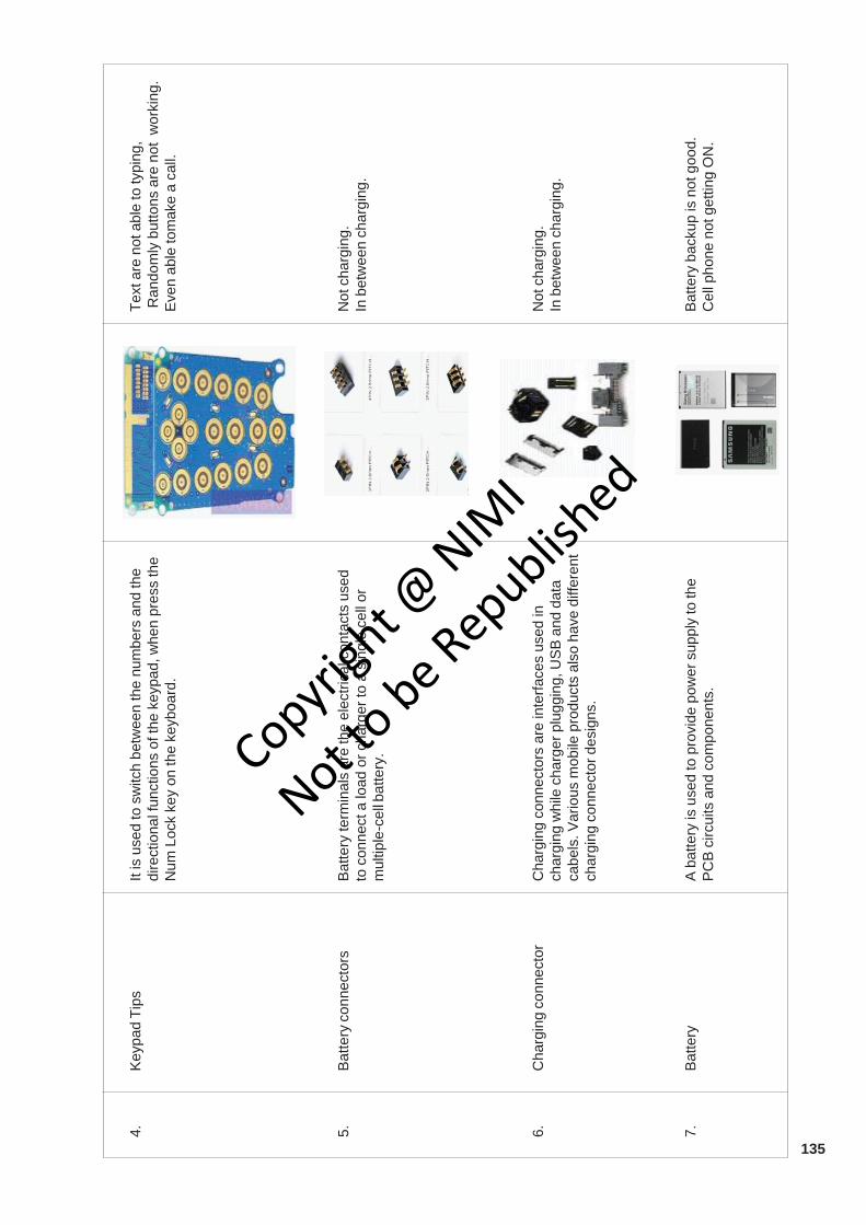
135
4.K
eypa
d Ti
psIt
is u
sed
to s
witc
h be
twee
n th
e nu
mbe
rs a
nd th
eTe
xt a
re n
ot a
ble
to ty
ping
,di
rect
iona
l fun
ctio
ns o
f the
key
pad,
whe
n pr
ess
the
Ran
dom
ly b
utto
ns a
re n
ot w
orki
ng.
Num
Loc
k ke
y on
the
keyb
oard
.E
ven
able
tom
ake
a ca
ll.
5.B
atte
ry c
onne
ctor
sB
atte
ry te
rmin
als
are
the
elec
trica
l con
tact
s us
edN
ot c
harg
ing.
to c
onne
ct a
load
or c
harg
er to
a s
ingl
e ce
ll or
In b
etw
een
char
ging
.m
ultip
le-c
ell b
atte
ry.
6.C
harg
ing
conn
ecto
rC
harg
ing
conn
ecto
rs a
re in
terfa
ces
used
inN
ot c
harg
ing.
char
ging
whi
le c
harg
er p
lugg
ing,
US
B a
nd d
ata
In b
etw
een
char
ging
.ca
bels
. Var
ious
mob
ile p
rodu
cts
also
hav
e di
ffere
ntch
argi
ng c
onne
ctor
des
igns
.
7.Ba
ttery
A ba
ttery
is u
sed
to p
rovi
de p
ower
sup
ply
to th
eB
atte
ry b
acku
p is
not
goo
d.P
CB
circ
uits
and
com
pone
nts.
Cel
l pho
ne n
ot g
ettin
g O
N.
Copyrigh
t @ NIM
I
Not to be Republish
ed

136
8.S
im S
lot
This
is a
n in
terfa
ce th
at a
cts
as a
hol
der a
nd c
onne
cts
No
inse
rtion
of s
imth
e si
m c
ard
to P
CB
circ
uit a
vaila
ble
in d
iffer
ent s
izes
Net
wor
k no
t ava
ilabl
elik
e m
icro
, nan
o si
m s
lots
.In
valli
d si
m
9.M
emor
y ca
rd s
lot
This
is in
terfa
ce th
at a
cts
as a
hol
der a
nd c
onne
cts
Inse
rt m
emor
y ca
rd th
e m
emor
y ca
rd to
PC
B c
ircui
t.N
o sp
ace
10.
Spe
aker
The
spea
ker c
onve
rts e
lect
rical
sig
nal i
nto
voic
e. N
ot a
ble
to h
ear t
he v
oice
of t
he
It is
als
o ca
lled
an e
arpi
ece.
callin
g pe
rson
dur
ing
a ca
ll.
11.
Mic
A m
ic c
onve
rts v
oice
into
ele
ctric
al s
igna
l.V
oice
will
not b
e he
ard
by th
e pe
rson
It is
als
o ca
lled
mic
roph
one
and
you
are
talk
ing
to. N
ot a
ble
to re
cord
mou
thpi
ece.
voic
e.
Copyrigh
t @ NIM
I
Not to be Republish
ed

137
12.
Rin
ger /
Buz
zer
A ri
nger
, als
o ca
lled
a lo
ud s
peak
erth
roug
h w
hich
you
hea
r rin
gton
e an
d m
usic
. Dur
ing
No
ring
tone
mus
ic o
r lou
da
call,
whe
n yo
u ac
tivat
e th
e lo
ud s
peak
er, t
he lo
uder
spea
ker's
voi
ce d
urin
g a
call
voic
e w
hich
you
sta
rt he
arin
g al
so c
omes
from
the
ringe
r. It
is a
lso
calle
d a
buzz
er in
bas
ic lo
w-e
nd m
obile
pho
nes.
13.
Ant
enna
Sw
itch
It is
foun
d in
the
Net
wor
k S
ectio
n of
a m
obile
pho
ne.
If th
e A
nten
na S
witc
h is
faul
ty th
en In
GS
M s
ets
it is
foun
d in
whi
te c
olor
and
ther
e w
ill b
e no
net
wor
k in
the
mob
ile in
CD
MA
set
s it
is fo
und
in g
olde
n m
etal
.ph
one.
It s
earc
hes
netw
ork
and
pass
es fo
rwar
daf
ter t
unin
g.
14.
P.F
.OIt
is fo
und
near
the
Ant
enna
Sw
itch
in th
e N
etw
ork
If th
e P
FO is
faul
ty th
en th
ere
will
beS
ectio
n o
f the
PC
B o
f Mob
ile P
hone
. It i
s al
so c
alle
dno
net
wor
k in
the
mob
ile p
hone
. If i
tP
.A (P
ower
Am
plifi
er) a
nd B
and
Pas
s Fi
lter.
gets
sho
rt th
en th
e m
obile
pho
ne w
illge
t dea
d.
It fil
ters
and
am
plifi
es n
etw
ork
frequ
ency
and
sel
ects
the
hom
e ne
twor
k.
15.
RF
IC /
Hag
ar /
This
ele
ctro
nic
com
pone
nt fo
und
near
the
PFO
in th
eIf
the
RF
IC is
faul
ty th
en th
ere
will
be
Net
wor
k IC
Net
wor
k S
ectio
n of
a M
obile
Pho
ne. I
t is
also
cal
led
RF
prob
lem
with
net
wor
k in
the
mob
ilesi
gnal
pro
cess
or.
It w
orks
as
trans
mitt
er a
nd re
ceiv
er o
fph
one.
Som
etim
es th
e m
obile
pho
neau
dio
and
radi
o w
aves
acc
ordi
ng to
the
inst
ruct
ion
can
even
get
dea
d.fro
m th
e C
PU
.
Copyrigh
t @ NIM
I
Not to be Republish
ed

138
16.
26 M
Hz
Cry
stal
It is
foun
d ne
ar th
e P
FO in
the
Net
wor
k S
ectio
n of
aIf
this
cry
stal
is fa
ulty
then
ther
e w
ill b
eO
scilla
tor
Mob
ile P
hone
. It i
s al
so c
alle
d N
etw
ork
Cry
stal
.no
out
goin
g ca
ll an
d no
net
wor
k in
the
It cr
eate
s fre
quen
cy d
urin
g ou
tgoi
ng c
alls
.m
obile
pho
ne.
17.
VC
OIt
is fo
und
near
the
Net
wor
k IC
in th
e N
etw
ork
Sec
tion
If it
is fa
ulty
then
ther
e w
ill b
e no
of a
Mob
ile.
It se
nds
time,
dat
e an
d vo
ltage
to th
e R
F IC
netw
ork
in th
e m
obile
pho
ne a
nd it
will
/ Hag
er a
nd th
e C
PU
. It
also
cre
ates
freq
uenc
y af
ter
disp
lay
“Cal
l End
” or “
Cal
l Fai
led”
.ta
king
com
man
d fro
m th
e C
PU
.
18.
RX
Filt
erIt
is fo
und
in th
e N
etw
ork
Sec
tion
of a
Mob
ile P
hone
.If
it is
faul
ty th
en th
ere
will
netw
ork
It fil
ters
freq
uenc
y du
ring
inco
min
g ca
lls.
prob
lem
dur
ing
outg
oing
cal
ls.
19.
RO
MIt
is fo
und
in th
e P
ower
Sec
tion
of a
Mob
ile P
hone
.If
RO
M is
faul
ty th
en th
ere
will
It lo
ads
curr
ent o
pera
ting
prog
ram
in a
Mob
ile P
hone
.so
ftwar
e pr
oble
m in
the
mob
ile p
hone
and
the
set w
ill ge
t dea
d.
Copyrigh
t @ NIM
I
Not to be Republish
ed

139
20.
RAM
It is
foun
d in
the
pow
er s
ectio
n of
a m
obile
pho
ne.
If R
AM
is fa
ulty
then
ther
e w
ill b
eIt
send
s an
d re
ceiv
es c
omm
ands
of t
he o
pera
ting
softw
are
prob
lem
in th
e m
obile
phon
e pr
ogra
min
a m
obile
pho
ne.
and
it w
ill ge
t fre
quen
tly g
et h
ange
dan
d th
e se
t can
eve
n ge
t dea
d.
21.
Flas
h IC
It is
foun
d in
the
Pow
er S
ectio
n of
a M
obile
Pho
ne.
If Fl
ash
IC is
faul
ty th
en th
eIt
is a
lso
calle
d E
EP
RO
M IC
, Mem
ory
IC, R
AM
ICm
obile
pho
ne w
ill n
ot w
ork
prop
erly
and
RO
M IC
. S
oftw
are
of th
e m
obile
pho
ne is
inst
alle
dan
d it
can
even
get
dea
d.in
the
Flas
h IC
.
22.
Pow
er IC
It is
foun
d in
the
pow
er s
ectio
n of
a m
obile
Pho
ne.
If P
ower
IC is
faul
ty th
en th
e se
t will
get d
ead.
It ta
kes
pow
er fr
om th
e ba
ttery
and
sup
plie
s to
all
othe
rpa
rts o
f a m
obile
pho
ne.
23.
Cha
rgin
g IC
It is
foun
d in
the
pow
er s
ectio
nIf
Cha
rgin
g IC
is fa
ulty
then
the
set w
illIt
take
s cu
rren
t fro
m th
e ch
arge
r and
cha
rges
the
batte
ry.
not g
et c
harg
ed. I
f the
Cha
rgin
g IC
issh
ort-c
ircui
ted
then
the
set w
ill g
etde
ad.
Copyrigh
t @ NIM
I
Not to be Republish
ed

140
24.
RTC
It is
Rea
l Tim
e C
lock
and
is fo
und
in th
e P
ower
Sec
tion
If R
TC is
faul
ty th
en th
ere
will
be n
o(S
impl
e S
ilicon
Cry
stal
)ne
ar P
ower
IC. I
t is
of lo
ng s
hape
.da
te o
r tim
e in
the
mob
ile p
hone
and
It he
lps
to ru
n th
e da
te a
nd ti
me
in a
mob
ile p
hone
.th
e se
t can
eve
n ge
t dea
d.
25.
CPU
It is
foun
d in
the
Pow
er S
ectio
n.
It is
als
o ca
lled
MA
DIt
cont
rols
all
sect
ions
of a
mob
ileIC
, RA
P IC
and
UP
P.
It is
the
larg
est I
C o
n th
e P
CB
of a
phon
e.M
obile
Pho
ne a
nd it
look
s di
ffere
nt fr
om a
ll ot
her I
Cs.
26.
Logi
c IC
/ U
I IC
It is
foun
d in
any
sec
tion
of a
mob
ile p
hone
. It h
as 2
0If
Logi
c IC
/ U
I IC
is fa
ulty
then
Rin
ger,
pins
or l
egs.
It is
als
o ca
lled
UI I
C a
nd In
terfa
ce IC
.V
ibra
tor a
nd L
ED
of m
obile
pho
ne w
illIt
cont
rols
Rin
ger,
Vib
rato
r and
LE
D o
f a m
obile
pho
neno
t wor
k pr
oper
ly.
27.
Aud
io IC
It is
foun
d in
Pow
er S
ectio
n of
a m
obile
pho
ne. I
t is
also
If A
udio
IC is
faul
ty th
en S
peak
er a
ndca
lled
Cob
ba IC
and
Mel
ody
IC. I
t con
trols
Spe
aker
and
Mic
roph
one
of a
mob
ile p
hone
will
not
Mic
roph
one
of a
mob
ile p
hone
.w
ork
and
the
set c
an e
ven
get d
ead.
Copyrigh
t @ NIM
I
Not to be Republish
ed

141
Data transfer among phone, internal and externalObjectives : At the end of this lesson you shall be able to• differentiate between internal and phone memory• describe SD card memory• explain the data transfer between phone memory and S.D card meory• explain how to interface the cell phone/smart to the PC and transfer data.
Internal Storage
There are three types of memory capacities in our smartphones these days: Internal, Phone and External. Thefirst two are often confused for each other while the thirdis still understood as SD card storage.
Internal memory used for installing the applications (theoperating system) and data. Applications are installed inthis storage and the personal data such as text messages,contact lists, email settings and the likes are stored onthis. This is considered to be quite sensitive informationand this is not accessible to user. Whenever the phoneis reset to factory settings, all this storage gets erased.This memory is reserved for the operating system andpersonal data. It will never show up whenever phone isconnected to computer.
Phone Storage
This is the storage that is available to user. This is thestorage that user get from the phone itself. Games andapplications are installed in this one and it is the defaultmemory for storing pictures, movies, songs and so on.User can access it when the phone is connected tocomputer.
When use most of internal storage, user will get anotification for low storage, asking to delete some files,even when user have most of phone storage empty. Thismessage will be triggered by a system file which storesits data on Internal Storage. If user attempt to downloadmore apps, they will be housed on phone storage. Souser can store apps on phone storage as well. It can alsodisable apps which prompt low storage message due tolack of storage space to refresh their app data.
External Storage
It is the external storage capacity of phone. It depends onthe compatibility of the memory card slot and to whatextent is it supported. In simpler terms, it is the storagewhich can be removed easily by user (memory card) andcan be used for storing pictures, music, videos and manymore. It may or may not be able to install applications onit. This is because some manufacturers allow for it whilesome don't. To an extent, even user's cloud storage canbe categorized as external storage.
Data transferring
The data in the cell phone is possible to transfer fromphone to SD memory or PC and vice versa. Even we cantransfers the same application (Apps) stored in phone toSD card for improving performance. Data transferring to/from cell phone.
1 Phone to SD card
2 Phone to PC
i Using data cable
ii Using card reader
iii Using wi-fi syncing
iv Using bluetooth
v Using e-mail
vi Using cloud storage
Application (App) transfer
Apps are transferable from phone memory to SD andvice versa for improving performance and using memoryefficiently. This is possible in Android base phonesmostly. This option is available at settings and applicationmanager. In application manager, consisting a tab formoving data. We can also delete the application byuninstalling the app.
Data transfer between phone and SD memory
The data or file in phone or SD card can inter-transferablein the cell phone. This can be achieved by simplyselecting and copying the data and pasting folder viewoptions are need to get by installing apps. The new foldercan create by simply selecting options.
Data transfer between phone and PC (Using datacable)
There are so many methods and techniques fortransferring data. In those, using data cable is the easiestmethod.
In this, data cable is connected between PC and phone.Most of the cases PC will detect the phone as a memorydevices. In some cases need to download the supportingfile from internet. It need to permit the PC to accessphone for accessing data. This can be automaticallyasks when the phone is connected to PC.
The data can copy or clag from phone to PC and viceversa, as like memory card (Pen drive).
Data transfer using card reader
The phone data can also be transferred by using cardreader. For this we need to ensure the data of phone isavailable in SD card memory. For this transfer data fromphone to SD card by copy and paste. Need to switch OFFthe phone before removing SD card. SD card can alsobe removed by unmounting the external memory inphone setting at memory section. The data in thememory is transferable by using card reader as pen drivein PC.
E& H : Electronic Mechanic (NSQF LEVEL - 5) - Related Theory for Ex 4.6.282 - 290
Copyrigh
t @ NIM
I
Not to be Republish
ed

142
Data transfer using wi-fi
If the PC can support wi-fi (in built), phone can transferdata simply by enabling wi-fi network. For this, somesoftwares for PC and apps like "SHARE IT" for phonemust be available in internet. For connecting wi-fi to thePC, external wi-fi cards are available in the market. Thisis faster than bluetooth method.
In this method, there is no need of any physical connectionbetween PC and phone. It is suitable for large files likevideo, audio, etc.
Data transfer using bluetooth
It is also similar to the wi-fi method. But for this methodthere is no special software or apps are needed to install.Most of the phones and PCs are supporting bluetooth. Insome cases PC needs bluetooth connecting device forenabling. It is slower than wi-fi method. But it is costeffective. It is suitable for small size of files like photos,text, etc.
Formatting and the need for formatting of cell phonesObjectives : At the end of this lesson you shall be able to• explain meaning of formatting of cell phone and the need for formatting• define virus• explain the signs of a phone infected by virus• protect the cell phone from virus• list the various steps to be followed to keep the handset secure from different malwares.
Formatting of mobile phone
Formatting a cell phone means erasing or deleting all thestored data and information like contacts, images,multimedia files, etc from the phone memory. Datastored in the memory card is not deleted, it will remainsafe during formatting.
In formatting the cell phone the operating system likeiOS, symbian, Windows or Android are not at all to bereinstalled unlike in computers. The OS is not affectedand it remains intact.
The procedure where we have to reinstall the OS is calledflashing in cell phone repair jargon. Which is very muchdifferent from formatting. So let us go ahead with formattinga phone and not get confused with flashing.
In general the process of formatting is usually donewhen there is any problem due to infection by a virus.
Virus
A mobile virus is nothing but a small software code writtenby some one to corrupt or damage the information storedin the mobile system.
The signs that the phone is infected by virus are:
1 Slow Functioning : The entire handset will becomevery slow. If you open the menu, it will load after 2-5seconds. Also all the software's and apps will takedouble the time to open. In short, the handset willstuck!
Data transferring using e-mail
This is a technique used for transferring data. Thismethod mostly used for long distance data transfer. Inthis simply mailing the required data file to self addressor some one address and this can be downloaded byopening email from PC or phone. But this methodrequires internet connection. It is having limitations of filesize due to email support. This can overcome by cloudstorage method.
Data transferring using cloud storage
This method is similar to e-mail method. But, hereinstead of email account, using cloud storage account.For this, so many third party cloud store operators areavailable in internet. They are offering large amount ofdata space for file storage. For data transfer, need toinstall cloud storage software in PC and App in phone.We can simply transfer data by upload method anddownloading. This method also required internetconnection.
2 Frequent Freezing : The device will freeze veryfrequently. It will get stuck all of a sudden and hang.Sometimes the handset will not even switch OFF. Ithas to restarted or remove the battery and insertagain.
3 Switching Off Automatically : Many times, thedevice will switch off automatically without informing.This will happen for more than 3-5 times a day!
4 Restarting: Sometimes instead of switching offautomatically, it will restart frequently.
5 Not Booting Properly : Sometimes, the virus cancorrupt the OS very badly, so that the cell phone willnot boot properly i.e. it will display a blank screen or itwill get stuck at the logo when switched on. It will notproceed further.
6 Failure of some apps : Some of the applications willnot function properly.
Protect a mobile phone from virus
A virus can infect your mobile phone the same way thatit infects computer. It will do the same damage like whata computer virus can do! It becomes very difficult tooperate when it gets infected with any malware, spyware,trojan or any other virus whether it is an android, Appleiphone, Blackberry or any other smartphone or a tablet.It is important to clean the infected phone from allbadware before it spreads. Protecting cell phone fromvirus is shown in Fig 1.
E& H : Electronic Mechanic (NSQF LEVEL - 5) - Related Theory for Ex 4.6.282 - 290
Copyrigh
t @ NIM
I
Not to be Republish
ed

143
Fig 1
Fig 2
Before knowing how to protect one should know thesources from which viruses can come and also takeprecautions so that it does not infect the gadget again.The best precaution against viruses is to install a reputedand updated antivirus program. If not, then one may endup getting the phone infected very soon.
The sources from which viruses can come in to thedevice are: (Fig 2)
1 Internet surfing: This is the most common source,especially if the user is visiting unknown and untrustedsites. The phone may most likely to get infected, if theuser visit untrusted websites.
2 MMC card: If you insert your memory card into a virusinfected gadget and then insert it back into yourphone, your handset will most likely get infected. Alsodo not put any other MMC card into your device,because if the other MMC has virus, it will spread intoyour device as well.
3 Bluetooth / Wi-Fi / Hotspot: While transferring filesto and from one phone to the other via bluetooth, WI-Fi or hotspot, when accept files from other phones,ensure that the user antivirus scans the incoming filesbefore opening them.
It is easy to keep your handset safe and secure fromdifferent malwares, if you follow these simple steps:
1 Install antivirus program and keep it updated:Always keep the bluetooth switched-off unlessrequired. Or it is preferable to keep the handset tohidden mode unless it needs to be visible.
2 Keep your bluetooth switched-off: Always keepthe bluetooth switched-off. If by fluke, the phone haskept on, do not accept any files from unknown sources.Still if the user have got any file by mistake NEVEROPEN SUCH FILE AS IT IS MOST LIKELY A VIRUS.Just delete the file.
3 Don't visit untrusted websites: While surfing theinternet, only visit the most trusted and reputedwebsites. Also if you have visited any unknown website,it's ok until you find it to be a suspicious one.
4 Don't download from untrusted sources: Surfingunknown websites is not as risky as downloadingcontent from them. Be careful of downloading any fileespecially if you find the website to be a suspiciousone. If you have downloaded anything, please do notopen that file and just delete it.
5 Be careful of the memory card: The MMC have tobe used carefully. So do not put your MMC in anotherhandset or anybody's MMC into your handset. It mightget infected easily and spread very fast.
Setting-up flashing filesObjectives : At the end of this lesson you shall be able to• define flashing of a cell phone and effects of cellphone after flashing• define flashing files• explain the availability of flashing files.
Flashing
Inside the cell phone handset, software is used to run andcontrol its different functions. Software makes the mobilehandset to function in a good and proper manner.
During the normal day to day operation, this software couldbecome corrupt and the phone will start to function in someunpredictable manner.
Phone could completely stop working or will start to showsome errors.
In this type of situation Universal Flash Storage (UFS)device can be used to reload the mobile phone with thecorrect software, so that the phone will once again startworking properly.
E& H : Electronic Mechanic (NSQF LEVEL - 5) - Related Theory for Ex 4.6.282 - 290
Copyrigh
t @ NIM
I
Not to be Republish
ed

144
This process of loading the mobile phone with correctsoftware using the UFS device is called “Flashing”.
This process is also known as “Software Repairing” ofthe mobile phones.
During the flashing process the UFS device sends somefiles to the cell phone. These files replace the corrupted/damaged file on the mobile phone and the phone willreturn to its proper state. This process is similar to theway operating system is reinstalled on a computer systemwhen it becomes corrupt.
Flashing files
Files sent by the UFS device to the mobile phone arecalled flashing files. These files contain the softwarerequired for proper operation of the mobile phone. Differentfunctions provided by the mobile phone depend on thesesoftware. These files could also contain ringtones,wallpapers and various operating commands.
When the flashing is done, the UFS device first removesexisting data and files from the mobile phone and thenthe new data and files are written.
Flashing files supported by some mobile are:
1 Nokia - MCU, PM, PMM, WUG, SLD, FBI, EEP, PP,MLF, RPL.
2 Samsung - MCU, AXF, OGM, MEL, S3, TFS, CLA,SRE.
3 Ericsson - MCU, MOD, GDF, PDA, LANG.4 Sony Ericsson - MCU, CUST/FS, GDF.5 Motorola-Acer - FLX, MCU, LP.
Availability of flashing files
When one buys UFS package, with the UFS box set offlashing cables and flashing software CDs are alsoprovided. The number of flashing cables and softwarereceived with the UFS package depends on the make/brand of the UFS package and also on how latest is thepackage being purchased.
For example, sometimes back one used to get 38 to 55flashing cables with the UFS package, but currentlyaround 60 flashing cables are provided with the latest
UFS-3 package.
One also gets around 25 CD with the latest UFS-3package. These CDs contain driver for UFS package,flashing software and flashing files for different make/model of mobile handsets.
Current UFS-3 device can be used to flash/repair morethan 400 models of Nokia, Samsung, Sony Ericsson, LG,Sharp, Motorola etc., make of handsets.
Flashing files required to flash/repair these mobilehandsets are provided on the CDs provided with the UFSpackage. Many of these flashing files are provided incompressed ZIP format on the CD.
Compressed files are files with file names ending withZIP, LZH, ARJ, or ARC, depending on how they werecreated. One need to decompress/extract these filesbefore using them, this decompression process iscommonly known as “Unzipping the file”.
Before using the ZIP files on the CD, you need to extractthem to some folder on the hard disk drive. For this youneed WinZip or WinRar program installed on yourcomputer.
Extracting these files on the hard disk drive will consumea lot of hard disk space, so you will require a computerwith large hard disk drive for mobile flashing purpose. Ifyou have limited hard disk space then you can extractfiles of only those mobile handsets which you requirefrequently. Other files can be extracted as and when theneed arises.
Flashing files of some of the mobile sets needs to beinstalled before using them. When looking at the folderon flashing CD, if you see application files, instead of ZIPfiles then that file needs to be installed.
Process to extract or install these files are explained laterin this book.One can also copy all the CDs received with the UFSdevice to some folder on the hard disk drive, and install/unzip them as and when required. This will be helpful ifyou misplace the CDs or CDs become corrupt due to anyreason (scratch etc.).
Various locks of cell phoneObjectives : At the end of this lesson you shall be able to• state the need of cell phone locks• explain different types of lock and unlock functions• describe lock and unlock functions in your cell phone.
Cell phone locks
Following are some of the locks which can be used incell phone. The various lock of the mobile handset isused for safety purpose.
1 Keypad Lock
2 Phone Lock
3 Security Lock
4 SIM Lock
Keypad Lock
As the name suggests, this lock will locks the handset’skeypad, one will not be able to use the keypad for any typeof number or text entry.
E& H : Electronic Mechanic (NSQF LEVEL - 5) - Related Theory for Ex 4.6.282 - 290
Copyrigh
t @ NIM
I
Not to be Republish
ed

145
Even when the keypad lock is active one can answerincoming call by pressing the keypad keys.
Different handsets use different method to enter intokeypad lock mode and to remove the lock. When thephone is in keypad lock mode, pressing of any key on thekeypad will display a message on the screen, explainingthe process to unlock the keypad.
Phone Lock
In this mode the handset cannot be used to make/receiveany call, even though the keypad stays active during thislock.
In this mode, when the handset is switched on, it asks foran unlocking code known as PIN or Personal IdentityNumber”. If this PIN is entered only it will work.
Security lock
Security lock is used to lock all the functions of the mobilehandset. When the security lock is on, the phone asks forthe PIN code when it is switched on.
Some handset may ask for the PIN number even whenthe SIM card of the phone is changed.
This facility is not provided on all handsets.
SIM Lock
When one buys a mobile handset from mobile serviceprovider under some scheme, the provider may lock thehandset with the SIM card in the phone.
This prevents the user from using the handset with SIMcard from some other service provider.
Currently, phones can be locked to accept only SIM cardsfrom one or more of the following:
1 Countries (your phone will work in one country, but notanother)
2 Network/Service providers (e.g. T-Mobile,Movistar,Vodafone etc)
3 SIM types (i.e. only specific SIM cards can be usedwith the phone).
Unlocking technology
A handset can be unlocked by entering a special code, orin some cases, over-the-air by the carrier.
Typically, a locked phone will display a message if arestricted SIM is used, requesting the unlock code.
For example, in some mobile phone, “Insert correct SIMcard” will appear on the phone’s display if the wrong SIMis used. Once a valid unlocking code is entered, the phonewill display “Network unlocked”. In some cases, the phonewill simply display a message explaining that it is locked.
The code required to remove all SIM locks from a phoneis called the master code or network code key.
The unlock code is verified by the phone itself, and iseither stored in a database or calculated using an obscuremathematical formula by the provider.
In some other mobiles embed a random number in thehandset’s firmware that is only retained by the network onwhose behalf the lock was applied. Such phones canoften still be unlocked, but need to be connected to specialtest equipment that will rewrite that part of its firmwarewhere the lock status is kept.
Most phones have security measures built in its softwarethat prevent users from entering the unlock code toomany times, usually four. After that the phone becomes“hard-locked” and special unlocking equipment has to beused in order to unlock it.
The main reason to unlock a phone is to be able to use itwith a different SIM card. For example, when travellingabroad it is usually cheaper to temporarily use a foreignnetwork, for example with a prepaid subscription. Contraryto some beliefs, an unlocked phone can’t access extracell phone towers or give free phone service. All it can dois accept other SIMs.
Unlocking via computer
One of the most popular way of phones are unlocked isusing the USB, RS-232 or LPT port of a computer usingsoftware usually written specifically for the model ofphone being unlocked. In some cases, special “unlockingclips” or “unlocking boxes” are used which re-program thesoftware that controls the phone, removing the SIM lock.However, such clips are usually very expensive.
Unlocking via Mail
Some companies have begun to offer a “mail-in” service,such as travelinsider.com. These services allow the userto send their phone in and have it sent back in an unlockedcondition.
Regulations on unlocking
Unlocking a phone without the permission or unlockingcode from the provider is usually in breach of the agreementwith the provider, though most countries do not makespecific laws prohibiting the removal of SIM locks.
Security lock
A security code is for the safety and security of your mobilephone. If you activate it in the security settings, the phonewill ask it while booting it every time or when you lock thekeypad and want to unlock the keypad.
The default security codes of major brands of cell phonesare as follows:
Samsung : 0000 / 00 00 00 / 00 00 00 00
Nokia : 12345
All other brands of cell phones : 0000 / 1234
Chinese brands : 1122 / 0000 / 1234 / 4321
So it is advisable to change the security code for safety.So if you change the security code, you should neverforget it. If you forget and put the wrong security code, thehandset will not accept it. So if you forget it and are unableto put the right code, your phone will be considered aslocked. You will have to get it unlocked by special software.
E& H : Electronic Mechanic (NSQF LEVEL - 5) - Related Theory for Ex 4.6.282 - 290
Copyrigh
t @ NIM
I
Not to be Republish
ed

146
Internet on cell phone and IMEI numberObjectives : At the end of this lesson you shall be able to• define internet and working of internet• define to acces the internet• explain some applications of internet from cell phone• define the IMEI NO and its importance• list the precaution to maintain the cell phone.
Internet
The Internet is a decentralised, international network ofnetworks.
Devices such as computers, mobile phones can connecteach other and form a network. The networks areconnected to each other through electronic, wireless andoptical networking technologies.
Multiple interconnected networks form the Internet.
Working of Internet
The Internet works based on protocols which handlechunks of data, known as "packets".
Various types of hardware, such as an ethernet networkcard or a modem, convert our device's binary packet datainto network signals and then back into packet data.
Internet Protocols(IP) are used to direct packets to aspecific computer or server.
Transmission Control Protocols (TCP) are used to directpackets to specific applications on a computer using aport number.
Accessing the Internet
We access the Internet because our router connects ourdevice to an Internet Service Provider (ISP).
Internet Service Providers (ISPs), such as Verizon, AT&Tand Comcast, give us access to the Internet through arange of technologies.
A single device is assigned an address when it connectsto the Internet: an Internet Protocol (IP) address. Thisaddress distinguishes our device in the network from allother devices.
However, our national ISP can only connect us directly toservers located in our country. If we want to connect toservers located in a different country, then we need thatcountry's ISP to connect us to those servers.
Protocols translate the text of our message into electronicsignals, transmit it through the network and translate itback into text once it reaches another device.
Data plan
Phones today have lots of features through the accessingof internet. You can check email, get directions, and evenchat over video. Ultimately, you can stay connected at alltimes. But in order to do so, your device needs to be ableto connect to the Internet to send and receive data.
If you're somewhere that offers Wi-Fi (like your house),staying connected is as simple as logging on to the server.
However, if you want to stay connected on the go, you'regoing to need a data plan to give you access to yourprovider's data network.
Navigation
GPS is a wonderful way to get around town. However,those map apps definitely use data. In order to find yourdestination, note your current location, and give you turn-by-turn directions, your GPS app needs to be connectedto the Internet.
Uploads
In order to upload and post a picture or video to socialmedia, you need to first be able to access it, whichrequires an Internet connection. While you can draftposts offline on some channels (like Facebook), yourdevice needs to be connected to the Internet through Wi-Fi or your cellular data network in order to actuallypublish.
Downloads
This is the process of receiving data over the internet. Itis the opposite of uploaders.
IMEI number
IMEI is short for International Mobile Equipment Identityand is a unique number given to every single mobilephone, typically found behind the battery. The IMEI is onlyused for identifying the device and has no permanent orsemi-permanent relation to the subscriber. Instead, thesubscriber is identified by transmission of an IMEI number,which is stored on a SIM card that can be transferred toany handset. However, many network and securityfeatures are enabled by knowing the current device beingused by a subscriber
IMEI numbers of cellular phones connected to a GSMnetwork are stored in a database (EIR - EquipmentIdentity Register) containing all valid mobile phoneequipment.
When a phone is reported stolen or is not type approved,the number is marked invalid.
The number consists of four groups that look similar tothis:
AA-BBBBBB-CCCCCC-D
AA - BBBBBB - CCCCCC - D
TAC Serial # Checksum
The Type Allocation Code (TAC) is the initial eight-digitportion of the 15-digit IMEI code used to uniquely identifywireless devices. The first two digits represent the country
E& H : Electronic Mechanic (NSQF LEVEL - 5) - Related Theory for Ex 4.6.282 - 290
Copyrigh
t @ NIM
I
Not to be Republish
ed

147
code. The second group of numbers identifies themanufacturer. The third set is the serial number and thelast single digit is an additional number (usually 0).
For example 99-000033-792410-8:
• 99 is country
• 000033 is manufacturer
• 792410 is the serial number
• 8 is the checksum value
How to check IMEI Number for your mobile:*06#
Mobile phone maintenance
Mobile phone is delicate device and needs care for itsproper functioning. Here are the common measures tokeep the mobile phone in good condition.
• Do not keep mobile phone in wet area or use it with wethands. Moisture can cause non-repairable internalcorrosion of parts.
• Do not drop the phone or damage the connectionpoints.
• Do not over stress the phone. It may damage thedisplay.
• Do not keep the phone near heat generating devices.High temperature in a car can damage its electronics.
• Do not over charge the battery. Charge the batteryonly its charge status goes below 50 percent.
• Prevent cloning.
Current technology of cell phones
Cell phone has the follwing special features;
a The fingerprinrt or iris scanners.
b New facial recognition technology which scans thecontours the person face and head.
c Unbreakable and foldable phones - The displayscreens are flexiable and hence it is foldable.
d Improved power backup - using nanobatteries,hydrogen fuel cells and solar power the power backuptime to the cell phones can be improved. The futurephones battery can also be charged improved. Thefuture phones battery can also be charged faster bywi-fi with the help of wireless signals and no need ofconventional power source/power bank.
e Contextual intelligence(also known as practicalintelligence) - The phones will use sensors to get dataabout your physical surroundings and conditions, usesaved information about you along with the contextualintelligence technology to make decisions for youeven before you thought of the question.
f Depth-sensing cameras-It provides 3D printing and3D scanning facility as shown in Fig.1.
Fig 1
Fig 2
g Multi-screen capabilities or screen casting - To connectand share the screen of the smartphone with thetablet, television or projector with no limitationsimposed by different platforms or OS, and irrespectiveof make or form as shown in Fig.2.
E& H : Electronic Mechanic (NSQF LEVEL - 5) - Related Theory for Ex 4.6.282 - 290
Fig 3
h Infrared support - Turn the smartphone into universalto operate the electronic and electrical gadget usingremote control as shown in fig.3. When this remotecontrol goes missing, we can give phone call and findout the remote/Cell phone.
i Dual recording - Existing smartphones come withfront and rear cameras but only one of them works ata time. Future smartphones may have better camerasupport to allow simultaneous recording using bothcameras.
j Besides the above features, there are numerous userfriendly apps with encriped security & hardware are
Copyrigh
t @ NIM
I
Not to be Republish
ed

148
developed to use the smartphone to function like &special device for a dedicated purpose also.
Advanced features in cell phones
Current technology cell phones has the following specialfeatures:
a The fingerprint or iris scanning.
b New facial recognition technology which scans thecontours the persons face and head.
c Unbreakable and foldable phones - The displayscreens are flexiable and hence it is foldable.
d Improved power backup - using nanobatteries,hydrogen fuel cell phones can be improved. The uptime to the cell phones can be improved. The futurephones battery can also be charged faster by wi-fi withthe help of wireless signals and no need of conventionalpower source/power bank.
e Contextual intelligence (also known as practicalintelligence) - The phones will use sensors to get datasaved information about you along with the contextualintelligence technology to make decisions for youeven before you thought of the question.
f IoT Technology - The smart phone can be used ascontrol device for IoT (internet of things) platformslike, to enable remote health monitoring andemergency notification systems, industrial controls,house hold appliances/gadgets/security monitoringand controlling, etc.
g Depth - sensing cameras - It provides 3D printing and3D scanning facility as shown in fig.1.
Fig 1
Fig 2
Fig 3
ANNEXTURE
Mobile Phone Related Abbreviations
In this article we expand common, and not so common,Mobile and Mobile Telephony abbreviations.
AC = Authentication Center;
ACRE = Authorisation and Call Routing Equipment;
A - GPS (also: AGPS) = Assisted - Global PositioningSystem;
AMOLED = Active Matrix Organic Light Emitting Diode;
E& H : Electronic Mechanic (NSQF LEVEL - 5) - Related Theory for Ex 4.6.282 - 290
h Multi-screen capabilities or screen casting - To connectand share the screen of the smartphone with thetablet, television or projector with no limitationsimposed by different platforms or OS, and irrespectiveof make or form as shown in fig.2.
i Infrared support - Turn the smartphone into universalremote controlto operate all the electronic and electricalgadgets using remote control as shown in fig.3. Whenthis remote control goes missing, we can give a phonecall and find out the remote/cell phone.
j Dual recording - Existing smartphones come withfront and rear cameras support to allow simultaneousrecording using both cameras.
Besides the above technical features, there are numeroususer friendly apps with encrypted security and hardwareare develped to use the smart phome accordigly tofunction like a special device for a dedicated purposealso.
AMPS = Analogue (Also: Advanced) Mobile PhoneSystem;
ANS = Advanced Network Services;
App(s) = Application(s);
BS = Base Station;
BSC = Base Station Controller;
BSS = Base Station System;
CAMEL = Customised Applications (for) Mobile-network
Copyrigh
t @ NIM
I
Not to be Republish
ed

149
Enhanced Logic (GSM / ETSI);
CDMA = Code Division Multiple Access;
(C)EIR = (Central) Equipment Identity Register; Blockedand Blocking and IMEI And Phone Identity.
CMAS - Commercial Mobile Alert Service;
CSIM = CDMA Subscriber Identity Module;
D-AMPS = Digital Advanced Mobile Phone Service;
EDGE = Enhanced Data (for) GSM Evolution;
EE = Everything Everywhere (Merger between T-Mobileand Orange);
EGSM = Extended Global System (for) Mobile;
EIR = Equipment Identity Register;
EMS = Enhanced Message Service;
ESN = Electronic Serial Number;
ETSI = European Telecommunications StandardsInstitute;
EUIMID = Expanded User Identity Module Identifier;
FAC = Final Assembly Code; IMEI And Phone Identity
GMSC = Gateway Mobile Switching Center;
GPS = Global Positioning System;
GPRS = General Packet Radio Services;
GPU = Graphics Processing Unit;
GSM = Global System (for) Mobile Communication;
GSMA = Global System (for) Mobile Association;
GSMS = GPRS Short Message Service;
GTP = GPRS Tunnelling Protocol;
ICCID = Integrated Circuit Card Identifier;
IMEI = International Mobile Equipment Identity;
IMEISV = International Mobile Equipment IdentitySoftware Version;
IMSI = International Mobile Subscriber Identity;
IMT2000 = International Mobile Telecommunications2000;
LAI = Local Area Identity;
LTE = Long Term Evolution;
MAG = Mobile Access Gateway;
MAP = Mobile Application Part;
ME = Mobile Equipment;
MEID = Mobile Equipment Identifier;
MCC = Mobile Country Code;
MIM = Mobile Instant Messaging;
MIN = Mobile Identification Number;
MMS = Multimedia Message Service;
MNC = Mobile Network Code;
MNO = Mobile Network Operator;
MNP = Mobile Number Portability;
MP3 = MPEG-1 Audio Layer-3 (Moving / Motion PictureExpert Group 3);
MP4 = MPEG-4 Part - 4 (Moving / Motion Picture ExpertGroup 4);
MPEG = Moving (Also: Motion) Picture Experts Group;
MS = Mobile Station;
MSC = Mobile Switching Centre(s);
MSE = Mobile Station Equipment;
MSIN = Mobile Station Identification Number;
MT = Mobile Terminated;
MTSO = Mobile Telephone Switching Office;
MVNA = Mobile Virtual Network Aggregators;
MVNE = Mobile Virtual Network Enabler;
MVNO = Mobile Virtual Network Operator;
N-AMPS = Narrowband - Advanced Mobile PhoneService;
NUC = Network Unlocking Code;
OMA = Open Mobile Alliance;
PAC = Port Authorisation Code;
PAYG = Pay As You Go;
PAYM =Pay Monthly;
PDA = Personal Digital Assistant; Also: Portable DigitalAssistant;
PIM = Personal Information Manager;
PIN = Personal Identification Number;
PLMN = Public Land Mobile Network;
PSTN = Public Switched Telephone Network;
GSM = Global System for Mobile Communication;
PUK = Pin Unlock Key;
RAM = Random Access Memory;
RIM = Research In Motion (The company behindBlackberry);
ROM = Read Only Memory;
R-UIM = Removable - User Identity Module;
SAP = SIM Access Profile;
S - GPS (Also: SGPS) = Simultaneous - Global PositioningSystem;
SIC = System Identification Code;
SIM = Subscriber Identity Module; SIM Card Facts
SMS = Small Message Service; Also: Short MessageService;
E& H : Electronic Mechanic (NSQF LEVEL - 5) - Related Theory for Ex 4.6.282 - 290
Copyrigh
t @ NIM
I
Not to be Republish
ed

150 E& H : Electronic Mechanic (NSQF LEVEL - 5) - Related Theory for Ex 4.6.282 - 290
SMSC = Small Message Service Center; Also: ShortMessage Service Center;
SMC-CS = Small (Also: Short) Message Control - CircuitSwitched;
SMC-GP = Small (Also: Short) Message Control - GPRSProtocol;
SMSMM = Small (Also: Short) Message Service MobilityManagement;
SMS - MO = Small (Also: Short) Message Service -Mobile Originated;
SMS - MT = Small (Also: Short) Message Service -Mobile Terminated;
SM-RL = Small (Also: short) Message - Relay Layer;
SM-TL = Small (Also: Short) Message - Transfer Layer;
SNS = Social Network Service (Also: Social NetworkServer)
TAC = Type Approval Code; or Type Allocation Code;IMEI And Phone Identity
TMSI = Temporary Mobile Subscriber Identity;
UI = User Interface;
UIMID = User Identity Module Identifier;
UMA = Unlicensed Mobile Access;
UMTS = Universal Mobile Telecommunications System(ETSI);
USIM = Universal Subscriber Identity Module;
USB = Universal Serial Bus;
VLR = Visitor Location Register;
VoIP = Voice over Internet Protocol;
WAP = Wireless Application Protocol;
Wi-Fi = Wireless Fidelity;
2G = 2nd Generation;
3G = 3rd Generation;
3G-MSC / VLR = 3rd Generation Mobile Switching CentreVisitor Location Register;
3GPP = 3rd Generation Partnership Project;
3G-SGSN = 3rd Generation Serving GPRS Support Node;
4G = Fourth (4th) Generation;
Copyrigh
t @ NIM
I
Not to be Republish
ed

151
Electronics & Hardware Sector Related Theory for Exercise 4.7.291 - 295Electronic Mechanic - LED Lights
Introduction of LED lightsObjectives : At the end of this lesson you shall be able to• define LED and the advantages of LED lights over other lighting systems• state the difference between LED lights and traditional lights• explain the parts and working of LED lights• describe the different colour generation in LED lights.
Introduction
The LED is used as a light source in our day to dayapplications. LED is the short form of "Light EmittingDiode". LEDs are basically electronic devices, made withsemiconducting material, which that emits light when it isconnected in forward bias mode. LED's properties aresimilar to general purpose diodes consisting of two leadscalled as anode and cathode. LED lights are energyefficient and having long life making them idealreplacements for traditional power halogen and standardincandescent lights.LED lights can save up to 90% ofhousehold lighting costs. Fig 1 shows LED symbol andlead identification.
Difference between traditional lights and LED lights
LED lighting differs from incandescent lamp and compactfluorescent lamp in several ways. When designed well,LED lighting can be more efficient, durable, versatile andlong lasting. Incandescent lamp produces light by use ofa filament. When current passing through a bulb, bulb willdissipate the power in the form of heat, thus producinglight. CFLs (compact fluorescent Lamps) are producinglight by exciting the mercury vapour held inside the lampwith electricity. LEDs produce light through a "coldprocess" when current flowing through the semiconductingmaterial (usually gallium, arsenic and phosphorus),electrons are able to recombine with holes within thedevice, releasing energy in the form of photons (i.e. light).This effect is called "electroluminescence".
LED working
Basically LED is a semiconductor device which is madewith P N junction. LED is used to convert current into lightwhen it is in forward biased condition. When LED is
forward biased, the electrons in N region are crossing thejunction and recombine with the holes in P region. Inenergy band diagram electrons are in conduction bandwhereas holes are in valance band as shown in Fig 2. Atthe time of electron hole recombination electrons aremoving from higher energy band(conduction band) tolower energy band (valancy band). So dissipate someamount of energy. This emitted energy will be in the formof light.
Parts of LED
The Fig 3(A) shows basic parts of LED and Fig 3(B)shows a power LED with heat sink.
When a LED connected to supply, current flows tosemiconductor chip through anode lead(1) and awhisker (4). The other side of the semiconductor isattached to the top of the anvil (7) and cathode (2). Thecolour of LED light depends on the material used formaking LED chip(5). There are no loose or moving partswithin the solid epoxy enclosure.
Copyrigh
t @ NIM
I
Not to be Republish
ed

152
The LED package will protect the LED chip from theoutside environment. The dissipated heat can betransferred by using a heat sink. The epoxy resinenclosure lens (3) has the following three functions.
1 It is designed to allow more light from thesemiconductor.
2 It focuses the light (viewing angle).
3 It protects the semiconducting material from the otherelements.
Colours of LEDs
LEDs are used to generate a monochromatic colour ofparticular wave length. The generated colour of LED isdepends upon the material used to make the LED chip.Unlike normal signal diodes, Light Emitting Diodes aremade from exotic semiconductor compounds such asGallium Arsenide (GaAs), Gallium Phosphide (GaP),Gallium Arsenide Phosphide (GaAsP), Silicon Carbide(SiC) or Gallium Indium Nitride (GaInN) all mixed togetherat different ratios to produce a distinct wavelength ofcolour.
The semiconductor material used will determine thewavelength of the photon light emission and the resultingcolour of the emitted light as shown in TABLE 1.
1 Gallium Arsenide (GaAs) - infra-red
2 Gallium Arsenide Phosphide (GaAsP) - red to infra-red, orange
3 Aluminium Gallium Arsenide Phosphide (AlGaAsP) -high-brightness red, orange-red, orange, and yellow
4 Gallium Phosphide (GaP) - red, yellow and green
5 Aluminium Gallium Phosphide (AlGaP) - green
6 Gallium Nitride (GaN) - green, emerald green
7 Gallium Indium Nitride (GaInN) - near ultraviolet,bluish-green and blue.
8 Silicon Carbide (SiC) - blue as a substrate
9 Zinc Selenide (ZnSe) - blue
10 Aluminium Gallium Nitride (AlGaN) - ultraviolet.
White light from LED
Unlike incandescent lamps, LEDs are not inherentlywhite light sources. LEDs emit highly efficient colouredlight for the applications such as traffic lights and exitsigns. General light source needs white light. In LEDwhite light can be achieved in three ways:
1 Phosphor conversion : In which a phosphor is usedon or near the LED is used to convert the colouredlight to white light as shown in Fig 4.
2 RGB systems: In which light from multiplemonochromatic LEDs (e.g., red, green, and blue) aremixed, resulting in white light as shown in Fig 4.
3 A hybrid method : In which uses both phosphor-converted (PC) and monochromatic LEDs.
Phosphor white light is more efficient than RGB white.
In the phosphor conversion method white light can beproduced by a single LED combining with a shortwavelength LED such as blue or UV, and a yellowphosphor coating. The blue or UV photons generated inthe LED either travels through the phosphor layer withoutalteration, or they are converted into yellow photons in thephosphor layer. The combinations of the blue and yellowphotons combine to generate white light.
TABLE 1
Typical LED characteristics
Sl.No. Semiconductor material Wavelength Colour VF @ 20mA
1. GaAs 850-940nm Infra-Red 1.2v
2. GaAsP 630-660nm Red 1.8v
3. GaAsP 605-620nm Amber 2.0v
4. GaAsPN 585-595nm Yellow 2.2v
5. AlGaP 550-570nm Green 3.5v
6. SiC 430-505nm Blue 3.6v
7. GaInN 450nm White 4.0v
E& H : Electronic Mechanic (NSQF LEVEL - 5) - Related Theory for Ex 4.7.291 - 295
Copyrigh
t @ NIM
I
Not to be Republish
ed

153
VI characteristics of LED
VI characteristics curve of a LED is shown in Fig 5.
To emit light in a LED needs a current flow through it, asit is a current dependant device with their light outputintensity being directly proportional to the forward currentflowing through the LED.
As the LED is to be connected in a forward bias conditionacross a power supply it should be a current limiter (usinga series resistor) to protect it from excessive current flow,it will destroy instantly because of too much current willpass through and burn it out. Generally 5mA is themaximum forward current for a simple LED and 30 mAfor a high bright light output LED.
From the TABLE 1 the characteristics of each LED hasits own forward voltage drop across the PN junction andthis parameter which is determined by the semiconductormaterial used for a forward current of 20mA.
LED Color guide
LED P/N Description Chemistry # of peak Dominant Forward voltageSuffix elements wavelength wavelength (Vf type) (Vf Max)
(χχχχχ/x-coord) (χχχχχ/y-coord)
H High efficiency red Gap 2 700 660 2.0 2.5
SR Super red GaAIAs 3 660 640 1.7 2.2
SR Super red AInGap 4 660 640 2.1 2.5
SI Super high intensity red AInGap 4 636 628 2.0 2.6
I High intensity red GaASP 3 635 625 2.0 2.5
Zi TS AllnGap red AInGap 4 640 630 2.2 2.8
SO Super orange AInGap 4 610 602 2.0 2.5
A Amber GaAsP 3 605 610 2.0 2.5
SY Super yellow AllnGap 4 590 588 2.3 2.8
ZY TS AllnGap yellow AllnGap 4 590 589 2.1 2.5
Y Yellow GaAsP 3 590 588 2.2 2.6
SUG Super ultra green AllnGap 4 574 568 2.2 2.6
G Green Gap 2 565 568 2.2 2.6
SG Super green Gap 2 565 568 2.2 2.5
G Pure green Gap 2 555 555 2.1 4.0
UPG Ultra pure green InGaN 3 525 520 3.5 4.0
UEG Ultra emerald blue InGaN 3 500 505 3.5 4.0
USB Ultra super blue InGaN 3 470 470 3.5 4.0
UV Ultra voilet InGaN 3 410 - 3.5 4.0
SUV Super voilet InGaN 3 380 - 3.4 3.9
E& H : Electronic Mechanic (NSQF LEVEL - 5) - Related Theory for Ex 4.7.291 - 295
Copyrigh
t @ NIM
I
Not to be Republish
ed

154
T Turquoise InGaN 3 0.19 0.41 3.2 4.0
V Voilet/Purple InGaN 3 0.22 0.11 3.2 4.0
P Pink InGaN 3 0.33 0.21 3.2 4.0
MW(Warm) Warm white InGaN 3 - - 3.2 4.0
NW(Neutral) Neutral white InGaN 3 - - 3.3 4.0
UW (Cool) Cool white InGaN 3 - - 3.3 4.0
LED efficiency, comparision with CFL and incandescent lampsObjectives : At the end of this lesson you shall be able to• compare LED lights and traditional lighting system• state the characteristics for the LED lighting system• list the advantages of LED lighting system• state the limitations of LED lighting system.
LED efficiency, comparison with CFL andIncandescent lamps
Many types of lighting systems are available such asincandescent lamps , fluorescent lamps and LED lamps.Incandescent lamps are traditional and available fromlong back. These are bulky in size, more power consumingthan others and having less life span. The compact
florescent lamps are popular due to more efficient , highillumination, more life span, less power consumptionthan incandescent lamps.
Now a day's LED lights are more popular and emergingtechnology in lighting systems. TABLE 1 gives thecomparison between these three lighting systems byvarious aspects.
Comparison chart
LED lights vs Incandescent light bulbs vs. CFLs
TABLE 1
I. Energy efficiency & Energy costs
1. Life span (Average) 50,000 hours 1,200 hours 8,000 hours
2. Watts of electricity used 6 - 8 watts LEDs use 60 watts 13 - 15 watts(equivalent to 60 watt bulb) less power (watts) per
per unit of light gener-ated(lumens). LEDshelp to reduce greenhouse gas emissionsfrom power plants andlower electric bills.
Sl. No. Particulars LED light Incandescent Compact Flourescent lamp Lamp(CFL)
3. Kilo-watts of electricity used (Equi- 329 KWh/yr. 3285 KWh/yr. 767 KWh/yr.valent to 30 Incandescent bulbs peryear)
E& H : Electronic Mechanic (NSQF LEVEL - 5) - Related Theory for Ex 4.7.291 - 295
Copyrigh
t @ NIM
I
Not to be Republish
ed

155
Sl. No. Particulars LED light Incandescent Compact Flourescent lamp Lamp(CFL)
II. Environmental impact
1. Contains the TOXIC Mercury No No Yes - Mercury(equivalent to 60 watt bulb) is very toxic to
health andthe environment.
2. RoHS complaint Yes Yes No - Contains 1 mg- 5 mg of mercuryand is major risk tothe environment.
Carbon-di-oxide emissions(30 bulbs per year)Lower energy consumption 451 pounds/year 4500 pounds/year 1051 pounds/year
3. decreases: CO2emissions, sulphur oxide andhigh-level nuclear waste.
III. Important facts
1. Sensitivity to low None Some Yes - may not worktemperatures under negative 10
degrees fahrenheitor over 120degrees fahrenheit.
2. Sensitive to humidity No Some Yes
3. Turns on instantly Yes Yes No - takes time towarm up
5. Heat emitted 3.4 btu's / hour 85 btu's / hour 30 btu's / hour
6. Failure modes Not typical Some Yes - may catch onfire, smoke, oremit an odor.
Sl. No. Particulars LED light Incandescent Compact Flourescent lamp Lamp(CFL)
4. Durability Very durable Not very durable Not very durable -glass or filament glass can breakcan break easily. easily.
E& H : Electronic Mechanic (NSQF LEVEL - 5) - Related Theory for Ex 4.7.291 - 295
Copyrigh
t @ NIM
I
Not to be Republish
ed

156
IV. Light output
1. Lumens Watts Watts Watts
2. 450 4 - 5 40 9 - 13
3. 800 6 - 8 60 13 - 15
4. 1100 9 - 13 75 18 - 25
5. 1600 16 - 20 100 23 - 30
6. 2600 25 - 28 150 30 - 55
Sl. No. Particulars LED light Incandescent Compact Flourescent lamp Lamp(CFL)
Characteristics of LED lights
1 Colour quality
2 Light output
3 Less power consumption
4 High efficiency
5 Long lifetime
6 Smallest in size
7 High resistance to switching cycles
8 Immediate light at switching on
9 Wide operating temperature range
10 High impact and vibration resistance
11 No UV or IR radiation
12 High colour saturation level without filtering
13 Mercury-free
Lifespan of LED Lighting
All the lighting sources having different expected lifespanunder various laboratory test conditions. Manufacturerswill provide these information on their product packageson hours basis. In TABLE 2 shows the expected lifespanof various lights.
The life of LED is about 10 to 25 times higher thanincandescent lamp and 2 to 5 times than CFL's. So, LEDbulbs are good for long time considerations. TABLE 3shows some calculation regarding operational cost ofvarious lighting systems.
Types of bulbs Expected lifetime
Incandescent Bulbs Between 750 and 2,000 hrs.
Compact Fluorescent Between 6,000 and 10,000hrs. Lamp (CFL)
LED Lights Between 20,000 and 50,000 hrs.
TABLE 2
Aspect Incandes- CFL LED cent
Approximate cost per bulb Rs. 20/- Rs.100/- Rs 250/-
Average lifespan 1,200 hrs 8,000 hrs 25,000 hrsWatts used 60 W 15 W 10 WNo. of bulbs 20 3 1
needed for 25,000 hrs of useTotal purchase Rs.1200/- Rs.300/- Rs. 250/-
price of bulbs (25,000 Hrs.)Total cost of Rs.4500/- Rs.1125/- Rs. 750/-
electricity used (25,000 hours at Rs.3 per kWh)Total operational
cost over Rs. 5700/- Rs.1425/- Rs. 1000/- (25,000 Hrs.)
TABLE 3
E& H : Electronic Mechanic (NSQF LEVEL - 5) - Related Theory for Ex 4.7.291 - 295
Copyrigh
t @ NIM
I
Not to be Republish
ed

157
Advantages of LED Lighting:
LEDs are having a number of advantages when comparedto traditional lighting systems.
Durability of LED lights
Incandescent bulbs and fluorescent lamps will breakeasily when shaken or dropped. The incandescent bulbhas a filament that is likely to break in such a situation.The LED lights are made in robust design. They aresuffering considerably less degradation over time. Atypical LED light would be expected to lose only 2 per centof its total efficiency after a period of 10,000 hours.
The useful lifespan of LED lighting products is defineddifferently than that of other light sources, such asincandescent or CFL. This is because LEDs typically donot "burn out" or fail. Instead, they experience lumendepreciation, where the amount of light produceddecreases and light colour appearance can shift overtime.
LED lighting efficiency
Incandescent bulb and fluorescent lamp dissipate moreamount of energy, so that heat produced, because theydistribute light in many directions. By comparison, LEDlights operate at low temperature and produce morefocused form of light. A typical incandescent lamp operatesat an efficiency level of around 9 percent. LED light canachieve efficiency levels which is closer to 40 per cent.The LED lights can be manufactured in smaller sizes andcan be placed in spaces that would not be suitable forother forms of lighting.
Light output
Modern LED lights have the appropriate light output andcolour characteristics to exceed the performance levelsof incandescent bulbs. LED lighting can also be used inconnection with standard household dimmer switches,or with more flexible control systems, allowing coloursettings to be manipulated quickly.
Disposing of LED Lights
Unlike fluorescent bulbs, LED lights does not releasemercury into the air. Some studies have shown that, theyinclude a number of other toxic materials. When dealingwith a broken LED light, it is advisable to make use ofgloves and to be aware of the toxic nature of the materialsthat have been used in the manufacture of the lights.However, LED lights can be disposed at landfill sites.
Range of uses
LED Lights do not release out an Ultra Violet (UV) rays,which means that they can safely be used in situationswhere precious items need to be exhibited. An exampleof this might be in the case of lighting the paintings orother artifacts.The lack of UV rays means that insects arenot attracted to these light sources. This is particularlyuseful for the food industry and also for externalinstallations. It is also possible to create lighting in a widerange of colours, without the need of different colouredbulbs or filters. As a result, interesting effects can be
created using LED lighting, allowing for an element ofcreativity within domestic and commercial purposes.
Instant lighting
One of the drawback of traditional lighing is they does notlight up immediately. With LED lighting, there is no suchdelay. When switched on, they reach full brightness up to100 times faster than other alternatives. This featureensures that they are well suited to use in vehicles.
Less wiring required
LED lights operate with low voltage and current. So thesize (Gauge) of wire used for house wiring will be less.So the cost of wire bundle will be lesser in all aspects.
Health benefits
Fluorescent lamp can be replaced by the LED lights dueto flickering effect. Such an effect can be annoying, it canalso have more serious health implications. Migrainesufferers and epileptics may find that the use of LEDtubes more comfortable.
Lower maintenance costs
LED lights never needed to be replaced and maintenancecosts tend to be extremely low. It is rare for an individualLED to fail, if such a situation occurs, it does not meanthat the entire lamp will fail.
Directional light source
LEDs are "directional" light sources, which means theyemit light in a specific direction, unlike incandescent andcompact fluorescent bulbs, (which emit light and heat inall directions). For this reason, LED lighting is able to uselight and energy more efficiently in many applications.However, sophisticated engineering is needed to producean LED light bulb that emit light in all directions like anincandescent lamp.
A general purpose LED may not distribute light in alldirections if used in a table lamp.
Heat dissipation by LED
The LED lighting systems are not radiate heat as muchas an incandescent lamp or halogen bulb. This is usuallydone with the help of a heat sink, which is a passivedevice that absorbs the heat produced and dissipates itinto the surrounding environment. This keeps LEDs fromover heating and burning out. Thermal management isone of the most important factor for the successfulperformance of an LED product. Because the higher theoperating temperature of a LED more quickly the light willdegrade, and the shorter the useful lifespan will be.
Limitations of LED bulbs
1 The initial cost of LED bulbs are more. The price perlumen is very high than other types.
2 LED bulbs need a definite voltage and constant currentfor good results.
3 LED drivers are more costlier.
4 LED bulb colours are changing due to age and ambienttemperature.
E& H : Electronic Mechanic (NSQF LEVEL - 5) - Related Theory for Ex 4.7.291 - 295
Copyrigh
t @ NIM
I
Not to be Republish
ed

158
5 Two different white LEDs are not having same colourcharacteristics.
6 LED performance mostly depends on the correctengineering to manage the heat generated by the
LED. Which causes deterioration of the LED chipitself. Otherwise overheating the LED package,eventually leading to device failure. Adequate heat-sink is required to maintain long life.
Types of LED lightsObjectives : At the end of this lesson you shall be able to• list out the type of LED lights• explain the classification of low power LEDs• explain the classification of high power LEDs• list out the specification of LED lights.
Introduction
LED lights are mostly used for white colours in domesticand industrial applications. But in some other applicationswe need different colour LED lights in - red, orange,green, blue, etc.
Some LED lights are available in single colour, dualcolurs and multi-colour types. These multicolour lightsconsist of 2 or more colour LEDs in a board. By operatingexternal switches or by remote we can select the colourof LED lights . By selecting 2 or more colours we cangenerate various combinations of colours. Fig 1 showsthe symbols of different type of LEDs
2-Pin LED
The most common type of LED is the 2-pin, 5 mm, roundlens type. Generally these are a single LED. Polarity isindicated by the long lead (+/anode) or the flat on one sideof the base (-/cathode).
The two-pin package can contain a single or two back-back LEDs.
Be aware that bi-colour LEDs are also sold in thispackage. Some are dual-colour so that reversing thecurrent through them changes the colour. Others may
have both LEDs the same colour and this can be usefulin AC applications as it can conduct on both cycles of themains and eliminates the need for a rectifier.
The data sheet of the bi-colour LED provides the terminalconnection for the colours
3-Pin LED
The three-pin LED is usually a pair of LEDs of differentcolours sharing a common anode or common cathode.Either LED can be turned on independently or blended tocreate a combination.
A bi-colour, 3-pin, common-cathode LED is shown inFig 3
4-Pin LED
The 4-pin LED package is most commonly seen on RGB(Red-green-blue) LEDs. Common cathode and commonanode versions are available. It produces the red, greenand blue colours acros the visible spectrum, commoncathode type. The RED LED in a 4 pin package is shownin Fig.4
6-Pin
RGB with individual pinouts allows common anode,common cathode configuration as well as seriesconnection of the LEDs is shown in Fig 5
E& H : Electronic Mechanic (NSQF LEVEL - 5) - Related Theory for Ex 4.7.291 - 295
2(a) 2(b) 2(c)
A typical 2Pin LED
Copyrigh
t @ NIM
I
Not to be Republish
ed

159
When the number of Pins reaches six all sorts of strangevariations are possible to bring out each LED anode andcathode on individual pins. This allows a single part to beused to common anode, common cathode and seriesLED configurations.
A slightly modified 6-pin, RB-GB, LED, has two separate3-pin LEDs in one package as shown in Fig.6
LF5WAEMBGMDW, 6-pin, RB-GB LED has two 3-pinLEDs in one package. Both have a blue LED. Note thepin length orientation clue.
Classification of LED lights
A. According to the power level
LED lights are classified in to two categories. Those are
I. Low power LEDs or miniature LEDs
II. High power LEDs
I. Low power LEDs or miniature LEDs
These LEDs are more familiar as indicators in mobilephones, in television sets and in different types of digitaldevices. They are usually available in standard size &shape from 2 mm to 10 mm in hole and surface mountpackages. There is no need of separate heat sink. So itis compatible to different circuit boards. Different
E& H : Electronic Mechanic (NSQF LEVEL - 5) - Related Theory for Ex 4.7.291 - 295
Copyrigh
t @ NIM
I
Not to be Republish
ed

160
companies are manufacturing these LEDs in 5V and 12Vranges. Generally current rating about 1 mA to 20 mA.They are available in a "ready to fit" mode.
Common package shapes include round, with a domedor flat top, rectangular with a flat top, and triangular orsquare with a flat top as shown in Fig 2.
There are three main categories
1 Low-current
Typically rated for 2 mA at around 2 V (approximately 4mW consumption)
2 Standard
20 mA LEDs (ranging from approximately 40 mW to 90mW) at around:
i 1.9 to 2.1 V for red, orange, yellow, and traditionalgreen
ii 3.0 to 3.4 V for pure green and blue
iii 2.9 to 4.2 V for violet, pink, purple and white
3 Ultra-high-output
II. High power LEDs
These LEDs are the result of advanced semiconductortechnology. As the name indicates, these LEDs areknown by its high output. High-power LEDs (HP-LEDs) orhigh-output LEDs (HO-LEDs) can be driven at currentsfrom hundreds of mA to more than an ampere, comparedwith the other LEDs. LED power density up to 300 W/cm2
has been achieved. They are capable of producing lightoutput with higher luminous intensity. The HP-LEDsmust be mounted on a heat sink for heat dissipation. If theheat from a HP-LED is not removed, the device will fail inseconds.
High power LED's come in different shapes & sizes. Acommon example of high power LED in daily use is "LEDstrips" that are used for walls & room interiors.
Different types of LED lights are shown in Fig 3.
LED lights are made of arrays of SMD modules. Suchlights are made with standard shapes and fittings likeEdison screw base, MR16 shape with a bi-pin base, ora GU5.3 (bi-pin cap) or GU10 (bayonet fitting)etc. are asshown in Fig 4.(Refer page 167) They are compatiblewith the supply sockets. They included driver circuitry.
B. According to the shape LED lights are divided into 3 categories.
1 Spherical lights,
2 Tapered lights
3 Cup-shaped lights
C. LED tube lights
LED tube lights are designed to physically fit in fixturesinstead of fluorescent tubes. Some LED tube are suitablefor existing fixtures if appropriate ballast is used. An LEDtube light generally uses many individual Surface-MountedLEDs which are directional and require proper orientationto emit light in all directions around the tube. Most LEDtube lights can be used in place of T8, T10, or T12 tubedesignations, T8 is D26mm, T10 is D30mm, in lengths of590 mm (23 inch), 1,200 mm (47 inch) and 1,500 mm(59 inch).
D. LED strip lights
An LED Strip Light also known as an LED tape or ribbonlight. LED strip light is a flexible circuit made by surfacemounted light-emitting diodes (SMD LEDs) on a flexibletype PCB layers. These strips are usually comes with anadhesive agent in back. Previously, strip lights had beenused solely in accent lighting, backlighting, task lighting,and decorative lighting applications. Now a days due tothe increased luminous efficacy and longer life-spansLED strip lights are used in applications such as highbrightness task lighting, fluorescent and halogen lightingreplacements, indirect lighting applications, Ultra Violetinspection during manufacturing processes, costumedesign, etc.
E. SMD LEDs
Fig 5
SMD is short form of "Surface Mount Device", describesLED packages that can be mounted on a surface or aPCB by soldering method as shown in Fig 5. SMDs comein all shapes and sizes, and are typically described witha four digit number. 3528 SMDs and 5050 SMDs arepresently some of the most commonly used SMDs. Thefour digit numbers refer to the length and width dimensionsof the SMD, in this case, 3.5 x 2.8 mm and 5.0 x 5.0 mm,respectively.
E& H : Electronic Mechanic (NSQF LEVEL - 5) - Related Theory for Ex 4.7.291 - 295
Copyrigh
t @ NIM
I
Not to be Republish
ed

161
F. COB (chip on board) LED modules
These are LED lighting system have multiple LED chipsmounted on a single PCB, encapsulated in a phosphorepoxy mix. These modules can reach many hundredswatts, delivering over 10000 lumens. They can often beused in high-bay or exterior lighting.
LED light can be described in a number of ways
1 LED bulb shape
2 LED bulb diameter
3 LED bulb length
4 LED bulb base type
LED light bulb shape
It's shapes describe the general physical characteristicsof the LED light. LED light bulbs vary in shape from tubeshaped bulbs to funnel or pear shaped light bulbs. TheseLED light bulb shapes each have a code. For example: Tdesignates a 'tube', PAR signifies a 'parabolic aluminiumreflector' and MR is used for ‘multifaceted reflector’.
LED bulb diameter
The diameter of a light bulb is measured in two ways, inmillimetres and in 1/8th of an inch. The diameter for lightbulb shape is measured at the point of maximum size.Examples are: T12 is 12 eights of an inch or 12/8 = 1.5inches in diameter, PAR20 is 20 eighths of an inch indiameter or 2.5 inches, MR16 is 16 eighths = 16/8 = twoinches in diameter.
LED light bulb length
LED light bulb length is the overall length measured,typically in electrical connection, from base to the tip ofthe bulb. Or in the case of Tube from end to end. This canbe in metric or in inches or feet as shown in Fig 5.
Bulb base types
LED light bulb base types are typically measured by typeand diameter in millimetres. For example a typical Edisonmedium screw-in base like E27 is 27 millimetres indiameter. LED bi-pin bases, like a fluorescent tubereplacement or a bi-pin MR16, are measured betweenthe centres of each pin.
Size of LED on strip
The light output (lumen output) and light patterns aredepending on the size of LEDs on strips. Integral LEDstrips are available with two sizes
E& H : Electronic Mechanic (NSQF LEVEL - 5) - Related Theory for Ex 4.7.291 - 295
Copyrigh
t @ NIM
I
Not to be Republish
ed

162
1 35:28 - this indicating LED size as 3.5mm x 2.8mmLED. These are suitable for domestic applications likecabinet decoration, stairs , windows , photos, celingcoves etc.
2 50:50 - this is indicating LED size as 5.0mm x 5.0mmLED. These are bright LED strips and the size will beabout 40% bigger than 35:28 LEDs. These producinghigh light output. These can use for both commercial
and domestic applications such as outdoor lighting,ambient lighting for commercial areas, wall washersetc.
Number of LEDs per meter
The number of LEDs per metre affects the brightness(lumens) and light pattern of a strip. Integral LED stripsare available in three variations:
E& H : Electronic Mechanic (NSQF LEVEL - 5) - Related Theory for Ex 4.7.291 - 295
Copyrigh
t @ NIM
I
Not to be Republish
ed

163
1 30 LEDs/m - generally using domestic decorationslike kitchen kick plates, etc.
2 60 LEDs/m - task lighting, under kitchen cabinets, bartops, steps/staircase edging, doorway frames.
3 120 LEDs/m - high ceiling coves, exterior edge lighting,path ways, signage.
LED cut marks are normally 3 LEDs apart. The distancebetween cut marks will depend on the number of LEDsper metre.
Thermal management of high-power LEDs
High power light-emitting diodes (LEDs) can use 350milliwatts or more in a single LED. Most of the electricityin an LED becomes heat rather than light (about 70%heat and 30% light). If the dissipated heat is notremoved, the LEDs operates at high temperatures will
causes to lowers their efficiency, and reliability. So it isnecessary to keep the temperature with in safe limit andremove excess heat form the light for improving itslifespan and accuracy.
The excess temperature of LED light can be eliminatedby
1 Using heat adhesive with boards and heat sinks.
2 Heat sinks : The thermal conductive type materials(eg. aluminium) are using with LEDs which aredissipating heat by conduction methods. The shapeand size of heat sink also effects the speed of heatdissipation.
i Surface finishing of a heat sinks effecting the heatdissipation. A painted surface having more heatemmition than unpainted and unfinished one.
E& H : Electronic Mechanic (NSQF LEVEL - 5) - Related Theory for Ex 4.7.291 - 295
Copyrigh
t @ NIM
I
Not to be Republish
ed

164
ii Mounting methods also effect the cooling system.Heat-sink mountings with screws or springs areoften better than regular clips, thermal conductiveglue or sticky tape.
LED lamp specifications
It is important to know the specifications of LED lights forits selection . LED lights having so many specificationsin those more important specifications are as givenbelow.
1 Power rating
2 Equivalent incandescent lamp rating
3 Operating voltage and frequency
4 The light colour emitted
5 Its colour rendering index (CRI)
6 Luminous flux
7 Operating life time
8 Fitting type and whether the lamp is dimmable
9 In the case of directional lamps, the luminous intensityand beam angle may also need to known.
LED stacks - Connections, Driver circuitsObjectives : At the end of this lesson you shall be able to• describe the LED panel materials• explain the stacking of LED• explain the working of LED driver circuits.
The main materials of LED panel light structure areas follows
1 Aluminum frame
AL6063, aluminum extrusion mold is used due to lowinitial investment cost, good surface appearance, goodheat dissipation.
2 Diffuser plate
Installation of diffusion plate is used to invisible thescreen dot. Diffuser plate generally uses acrylic diffuserplate or PC 2.0 materials. Acrylic diffuser plate is lowcost, higher light transmission than PC 2.0 and is poor inanti-aging. The price of PC 2.0 is slightly higher, but it isgood at anti-aging. Acrylic diffuser plate light transmissionrate is 92% and that of PC 2.0 is 88%. We can choosethe materials of diffuser plate according to differentrequirement and usually use the acrylic materials.
3 Light guide plate
To emit the uniform light, light guide plate plays animportant roll in blocking the screen dot. The side LEDlight changes the angle of light ray by light refraction ofscreen dot. Light guide plate is the heart of the LED panellight and its screen dot design is very important. If thescreen dot design is not good, the overall lighting effectwill be bad like 1. Bright in the middle and dark in bothsides. 2. Bright in the bright side and dark in the middle.
4 Rear cover
Sealing lamp body usually uses aluminum. It plays a roleof dissipating heat and protecting the light.
5 LED lighting source
3528 is the usual light source. Besides, there are 5630and 5050. The luminous efficiency of 5630 and 5050 isnot high and the design of their screen dot is difficult buttheir cost is lower. The lighting effect of 3528 is high andthe screen dot is in acceptable range.
6 Drive power
There are two kinds of power modes: first, directly usingcross-flow power (this mode has high efficiency and PFvalue is up to 0.95, so it is cost-effective);second, constantpressure with cross-flow mode (this mode is stable, butwith low efficiency and high cost).
LEDs in series
We can connect LED's together in series to increase thelight level. If LED's are connected in series all have thesame forward current flow as shown in Fig 1.
Although, the series voltage drop across them needs tobe considered when calculating the required value of thecurrent limiting resistor, Rs. If we assume that each LEDhas a voltage drop of 1.2V across its when it is illuminatedthen the voltage drop across three will be 3x1.2v=3.6 volts. Consider that the supply voltage is 5 volt witha forward current of about 10mA. The value of seriesresistance Rs. will be calculated as:
VLED = 3 x 1.2 volts = 3 x 1.2 V = 3.6 V
RS = VS - VLED = 5 - 3.6 = 1.4 volts
RS = 10mA1.4v = 140 W
E& H : Electronic Mechanic (NSQF LEVEL - 5) - Related Theory for Ex 4.7.291 - 295
Copyrigh
t @ NIM
I
Not to be Republish
ed

165
Stacking of LEDs
Stacking means grouping of LEDs. LEDs may beconnected in series, parallel or series - parallelcombinations. It is necessary in each stacking that a LEDis operated at its rated DC voltage and the current passedthrogh a LED does not exceed to its rated value. Thevoltage rating of LEDs ranges from 1.6V to 4.2V and thecurrent rating ranges from 2mA to 20mA.
1 Parallel stacking
In this stack, all the LED are connected in parallel to asingle source of supply with a current limiting resistor foreach LED. Decorative lighting strip may contain anynumber of LEDs that are connected in parallel with acurrent limiting resistor for each LED.
2 Series-parallel stacking
LED light panels generally contain a parallel group ofsome series groups. Each series group usually contains3 to 4 LEDs. These panels may be of built-in type ormounted type.
3 Series stacking
In this stack, LEDs are connected in series, but usuallymore than 3-4 LEDs are not connected in series. Ofcourse, some series groups of 3-4 LEDs may beconnected in parallel. The reason behind it is differentvoltage distribution and current limiting of LEDs.
Driving of LED stacks
Here, driving means to apply DC supply to a stack (group)of LEDs. In general, a current limiting resistor is used witheach LED.
1 Driving a single LED
For driving (operating) a single 3 resistors. In the givenFig 3, only two groups of 3 LEDs each are shown, butthere are 24 such groups. IC 555 is used to limit the,circuit current at 10mA.
2 Driving a stack of 72 LEDs
For driving a stack of 72 LEDs, IC 555 may be used. 72LEDs are divided into 24 groups of 3 LEDs connected inseries and all the 24 groups are connected in parallelacross an IC 555 and 12 volts DC source. A currentlimiting and voltage dropping resistor of 82 ohms is usedin each group of 3 resistors. In the given figure, only twogroups of 3 LEDs each are shown, but there are 24 suchgroups. IC 555 is used to limit the, circuit current at 10mA.
3 Other driving circuits
A number of LEDs stack driving circuits have beendeveloped which employ different ICs. A current limitingresistor is necessarily connected in series of a single LEDor a series group of 3-4 LEDs.
Driver circuit
Fig 2
E& H : Electronic Mechanic (NSQF LEVEL - 5) - Related Theory for Ex 4.7.291 - 295
Copyrigh
t @ NIM
I
Not to be Republish
ed

166
LED drivers and its typesObjectives : At the end of this lesson you shall be able to• explain the need for a LED driver• list out the types of LED drivers• explain the factors to be considered to choose a LED driver• describe the working of LED driver circuit.
Need for a LED Driver
LED light sources require specialized devices called LEDdrivers to operate. LED drivers (also known as LEDpower supplies) are similar to ballasts for fluorescentlamps or transformers for low voltage bulbs: they provideLEDs with the electricity they require to function andperform at their best.
LEDs require drivers for two purposes:
1. LEDs are designed to run on low voltage (12-24V),direct current electricity. However, most places supplyhigher voltage (120-270V), alternating currentelectricity. An LED driver rectifies higher voltage,alternating current to low voltage, direct current.
2. LED drivers also protect LEDs from voltage or currentfluctuations. A change in voltage could cause a changein the current being supplied to the LEDs. LED lightoutput is proportional to its current supply, and LEDsare rated to operate within a certain current range(measured in amps). Therefore, too much or too littlecurrent can cause light output to vary or degradefaster due to higher temperatures within the LED.
In brief, LED drivers convert higher voltage, alternatingcurrent to low voltage, direct current. They also keep thevoltage and current flowing through an LED circuit at itsrated level.
Internal vs. External drivers (Fig 1)
For the aforementioned reasons, every LED light sourcerequires a driver. However, some LEDs, particularlythose designed for household use, contain internal driversrather than separate, external drivers. Household bulbsusually include an internal driver because it makesreplacing old incandescent or CFL bulbs easier. Thefigure 1 shows the external and internal drivers.
Choosing an LED Driver
There are two main types of external LED drivers,constant-current and constant-voltage, as well as a thirdtype of driver called an AC LED driver. Each type of driveris designed to operate LEDs with a different set ofelectrical requirements. When replacing a driver, the olddriver's input/output requirements must be matched asclosely as possible.
Constant-Current drivers
Constant-current drivers power LEDs that require a fixedoutput current and a range of output voltages. There willbe only one output current specified, labeled in amps ormilliamps (350mA, 700mA or 1A), along with a range ofvoltages that will vary depending on the load (wattage) ofthe LED.
Constant-Voltage Drivers
Constant-voltage drivers power LEDs that require a fixedoutput voltage with a maximum output current. In theseLEDs, the current is already regulated, either by simpleresistors or an internal constant-current driver, within theLED module. These LEDs require one stable voltage,usually 10 V, 12V DC or 24V DC.
AC LED Drivers
LEDs have such a small electrical load that regulartransformers do not register that they're wired to a bulb atall. AC LED drivers are typically used with bulbs thatalready contain an internal driver that converts the currentfrom AC to DC, so an AC LED driver's job is to register thelow wattage of LEDs and step down the voltage to meetthe bulb's voltage requirements, usually 12 or 24 volts.AC LED drivers are typically used to power 12-24V ACinput LED MR16 bulbs.
Fig 1
Internal LED driverExternal LED driver
E& H : Electronic Mechanic (NSQF LEVEL - 5) - Related Theory for Ex 4.7.291 - 295
Copyrigh
t @ NIM
I
Not to be Republish
ed

167
Factors to be considered to choose a LED driver
Max Wattage
According to the NEC (National Electrical Code), LEDdrivers should be paired with LEDs that use 20% lessthan their maximum rated wattage (with the exception ofAC LED drivers). Drivers should not be paired with anLED that is at or exceeds the driver's maximum wattageto avoid overstressing the driver components. Forexample, if you have a driver that can operate a maximumof 96 watts, it should only operate LEDs that use 77 wattsat most (96 x 0.8 = 76.8).
Dimming
Dimming functions are desirable to optimize illuminationas ambient light levels may change due to artificial ornatural variations in the lighting variations both indoorsand outdoors.
Both constant-current and constant-voltage LEDs anddrivers can be made with a dimming capability. Dimmableexternal drivers often require an external dimmer, orother dimming control devices to work. Since technologies
are improving rapidly, it's best to test specific LED/dimmable driver combinations for acceptable dimmingperformance.
Power Factor
Power factor describes how efficiently an LED driveruses electricity. The closer to 1 the power factor is, themore efficient the driver is. A good power factor is 0.9 orabove.
Ingress Protection (IP) Rating
IP ratings tell users the environmental protection that adriver's outer casing provides. The first number specifiesprotection against solid objects, and the second numberspecifies protection against water elements. For example,according to the chart below, a driver with an IP67 ratingis protected against dust and temporary immersion inwater.
Physical size and shape
Consider the physical dimensions of the driver. Makesure it will fit in the area you will place it.
IP Rating Chart
1st Digit Solid Object Protection 2nd Digit Water Protection
0 Not protected 0 Not Protected
1 Protected against solid objects 1 Protected against verticallygreater than 50mm dripping water(e.g. accidental bump of hand)
2 Protected against solid objects 2 Protected against sprays of watergreater than 12.5mm (e.g. fingers) when tilted up to 15 degrees vertically
3 Protected against solid objects 3 Protected against sprays of watergreater than 2.5mm (e.g. tools when tilted up to 60 degrees verticallyand wires)
4 Protected against solid objects 4 Protected against water sprayed ingreater than 1mm all directions(e.g. small wires)
5 Protected against dust 5 Protected against low-pressurejetting water from all directions
6 Dust tight (total protection) 6 Protected against powerfully jettingwater from all directions
7 Protected against temporaryimmersion in water (under30 minutes)
8 Protected against continuousimmersion in water
E& H : Electronic Mechanic (NSQF LEVEL - 5) - Related Theory for Ex 4.7.291 - 295
Copyrigh
t @ NIM
I
Not to be Republish
ed

168
Different schematics of driversObjective : At the end of this lesson you shall be able to• explain the working of a 230V led driver circuit.
A 230V LED Driver circuit without using a transformer isshown in Fig 2. 5 led's are used here, the count it can beincreased at your convineance. Due to the absence ofTransformers we can reduce the cost and size of thecircuit considerably. LED's are Cheap, efficient and cooldevice with low power consumption, so our electricity billswill be reduced to a great extent.
The circuit is powered by 230V 50Hz ac supply, so becareful while troubleshooting this circuit.
LED's commonly works only in DC, so we have to convertthe alternating current to direct current and step down toa safe value before applying to the led sequence.
The circuit mainly consisting of 5 LED bulbs, a bridgerectifier and a filtering network with voltage regulator.
The bridge rectifier is used to convert alternating current(AC) to pulsating DC. It is made possible by means ofrectifying diodes (D1 to D4 1N4007)
The filtering is made possible by means of a capacitor(47uF). It is used to eliminate the ripples coming fromrectifier circuit.
After regulating the filtered voltage using a zener diode,we get an almost direct current suitable for LED's.
A simple one more LED light driver circuit diagram isshown in Fig 3. In the above circuit diagram there is noprotection for surge current. In this circuit a surge protectiondevice a NTC has been included. There is in-rush surgecurrents flow in the circuit during power switch ON in anycircuit.
An NTC is attributed with a special property through whichit is able to raise its resistance significantly during powerswitch ON. When used in electronic circuits this propertyhelps blocking the initial surge currents in to the connectedcircuit. However in the process, the NTC becomes relativelywarmer, which brings down its resistance to lower levelssuch that the normalized safe power subsequently isallowed to pass over to the adjacent circuits.
Normally in an electronic circuit an NTC component isconnected with one of the mains supply line as shown inthe circuit diagram given below in series.
E& H : Electronic Mechanic (NSQF LEVEL - 5) - Related Theory for Ex 4.7.291 - 295
Copyrigh
t @ NIM
I
Not to be Republish
ed

169
Design a emergency light using LEDsObjectives : At the end of this lesson you shall be able to• state the brief idea about the emergency light• explain the working of the emergency light with charging circuit.
A simple LED emergency light circuit that can beimplemented for home lighting during power failures isgiven in the figure below. This LED lighting circuit designis intended to light automatically during main powerfailures. This circuit is a simple and low cost emergencylight. The main part of this LED light schematic is a relay,which automatically connects DC voltage to the batterywhen main power is present and connect LEDs to thebattery in the absence of mains AC power supply.
Working of Emergency light charger circuit
The step down transformer and the diode bridge rectifiersteps down and convert the high AC(in the range 230V)voltage to low (12V) DC voltage. The diode D5 preventsthe battery charge from flowing back, it acts as a freewheeling diode too.
In the presence of electricity, the relay contact connectsthe NO (Normally Open) terminal to battery. Thus batterycharges during this time. A red LED is used in the circuitas the charging indicator which glows when the emergencylight battery is charging.
When AC mains supply failure occurs, relay connects theNC (Normally Closed) terminal to the battery. If theswitch S1 is closed, the LED arrays are connected to NCterminal, thus they glow by using the charge stored in thebattery.
Whenever the emergency light is not used or not requiredto light, the switch S1 may be released, so that the LEDswill not glow.
To increase the brightness or light few more LEDs maybe connected in series and parallel.( series and parallelcombination)
E& H : Electronic Mechanic (NSQF LEVEL - 5) - Related Theory for Ex 4.7.291 - 295
Copyrigh
t @ NIM
I
Not to be Republish
ed

170
Electronics & Hardware Sector Related Theory for Exercise 4.8.296 - 303Electronic Mechanic - LCD & LED TV
Television transmitter and receiverObjectives : At the end of this lesson you shall be able to• explain the television broadcasting system• explain the television broadcast channel• state the three television systems used across/around the world.
Television broadcasting
The meaning of the word television "Tele" means at adistance, "vision" means to see the scene or a picture isfocused through a TV camera which converts the sceneor picture into images to electrical signal. The camera'soutput signal is modulated and transmitted aselectromagnetic waves along with respective sound as inFig 1.
(Phase Alternate Line) which is based on 625 lines 7 MHzchannel width with a line frequency of 50Hz. In "America"a system known as "NTSC" (National Television SystemsCommittee) is followed which is based on 525 lines,6MHz channel width operating on line frequency of 60 Hz."France" and some "European" countries follows a systemcalled "SECAM" (Sequential a memory) based on 625lines with 9 MHz band width.
A television based on one particular system cannot beused in other countries following a different system. Forexample a television used in America cannot be used inIndia. The present day Televisions have provision toselect one of the three systems so that the same TV couldbe used with different system in different countries.
Television broadcast channels
The band of frequencies used for video and audio signaltransmission is called a television channel.
TV signals are radiated at frequencies above 40 MHz.The VHF and UHF frequency bands that have beenassigned for the use of the TV stations are as follows.
Television channel
TABLE 1
Band I 41 MHz to 68 MHz channel 1 to 4
Band II 88 MHz to 108 MHz used for FMRadio broadcast
S-Band 104 MHz to 174 MHz
Band III 174 MHz to 230 MHz Channel 5 - 12known as VHF band
Hyper Band 230 MHz to 470 MHz and 2 to 20known as UHF
Band IV 470 to 582 MHz channel 21 to 36
Band V 606 to 870 MHz channel 37 to 69
Only band I and III are used for TV transmission in India.Each band is divided in to a number of channels. Accordingto the standards adopted in India each channel width is7 MHz.
TV transmitters are provided in different places to caterthe needs of the local population. Depending upon thearea to be covered either a low-power transmitter (LPT)or high power transmitter (HPT) is installed. A high powertransmitter can service an area of around 120Km and alow power transmitter around 20Km radius only.
The term broadcast means to send out in all directions.The transmitting antenna radiates electromagnetic waveswhich can be picked up by the receiving antenna. The TVtransmitter has two functions visual and soundtransmission. Both picture signal and the sound signalare emitted from the common radiating antenna.
The receiving antenna intercepts both the picture and thesound carrier signals. The signals are amplified and thendetected to recover the original modulation. Then thedetected video signal is amplified enough to drive thepicture tube.
There are three major television systems which arefollowed in different parts of the world. India and many ofthe "European" countries follows a system of "PAL"
Copyrigh
t @ NIM
I
Not to be Republish
ed

171
Scanning bandwidth composite video signalObjectives : At the end of this lesson you shall be able to• define scanning• explain different types of scanning• explain USB transmission and band width of TV signal.
Scanning
Scanning is the process of reading the scene rapidly bothin the horizontal and vertical directions simultaneously toprovide sufficient number of complete pictures or framesper second to give the illusion of continuous uniformmotion. Instead of 24 frames as is the practice incommercial motion pictures, the frame repetition rate is25 per second in most television systems.
Horizontal scanning
Fig 1 shows the trace and retrace of several horizontallines. The linear rise of current in the horizontal linedeflection coils as shown in Fig 2 deflects the beamacross the screen with a continuous, uniform motion forthe trace from left to right.
At the peak of its rise the saw tooth wave-reversesdirection and decreases rapidly to its initial value. Thisfast reversal produces the retrace or fiy back. The startof horizontal trace is at the left edge of raster. The finishis at the right edge and then the fly back produces retraceback to the left edge.
The heavy lines indicate useful scanning time and dashedlines correspond to the retrace time.
Vertical scanning
The saw tooth current in the vertical deflection coils asshown in Fig 3 moves the electron beam from top tobottom.
As shown in Fig 3 the trace part of the saw tooth wave forvertical scanning deflects the beam to the bottom of
E& H : Electronic Mechanic (NSQF LEVEL - 5) - Related Theory for Ex 4.8.296 - 303
Copyrigh
t @ NIM
I
Not to be Republish
ed

172
raster. Then the rapid vertical retrace returns the beam tothe top.
During vertical retrace, horizontal scanning continuesand several lines get scanned during this period. Becauseof motion in the scene being televised, the information atthe top of the picture tube screen normally changes bythe time the beam returns to the top to recommence thewhole process. This information is picked up during thenext scanning cycle and the whole process is repeated25 times per second to cause an illusion of continuity".
It must be noted that both during horizontal and verticalretrace intervals the scanning beams at the camera tubeand picture tube are blanked and no picture informationis either picked up or reproduced. These short retraceintervals are utilized for transmitting distinct narrow pulsesto keep sweep oscillators of the picture tube deflectioncircuits of the receiver in synchronization with those of thecamera at the transmitter. This ensures exactcorrespondence in scanning at the two ends and resultsin distortion less reproduction of picture details.
Interlaced scanning
Although the rate of 24 pictures per second in motionpictures and that of scanning 25 frames per second intelevision pictures is enough to cause an illusion ofcontinuity, they are not rapid enough to allow the brightnessof one picture or frame to blend smoothly into the nextthrough the time when the screen is blanked betweensuccessive frames. This results in definite flicker of lightthat is very annoying to the observer when the screenbecomes alternately bright and dark.
This problem is solved in motion picture by showing eachpicture twice so that 48 views of the scene are shown persecond although there are still the same 24 pictureframes per second. As a result of the increased blankingrate: flicker is eliminated.
In television pictures an effective rate of 50 vertical scansper second is utilized to reduce flicker, by making everyalternate line to get scanned instead of every successiveline. Then when the beam reaches the bottom of pictureframe at the end of the first scan, it quickly returns to thetop to scan those lines that were missed in the firstscanning. Thus the total number of lines are divided intotwo groups called as "Odd" field and "Even" field. Eachfield is scanned alternately. This method of scanning isknown as ‘Interlaced scanning.
In the 625 line TV system each frame or picture is dividedinto sets of 312.5 lines and each set is scanned alternatelyto cover the entire picture area. To achieve this thehorizontal sweep oscillator is made to work at a frequencyof 15625 Hz (312.5 x 50 = 15625), to scan the samenumber of lines per frame (15625/25 = 625 lines), but thevertical sweep circuit is run at a frequency of 50 Hz.
Note that since the beam is now deflected from top tobottom in half the time and the horizontal oscillator is stilloperating at 15625 Hz. The first field ends in a half lineand the second field commences at middle of the line ontop of the screen. The complete geometry of the standardinterlaced scanning pattern is shown in Fig 4.
The function of video amplifier is to provide sufficient gainto the video signal such that it can drive the picture tubefrom cut-off for blanking, to zero grid cathode voltage forpeak white. The peak to peak value of the video signalrequired to drive the picture tube vary depending on itssize. The video signal with range of video frequenciesfrom 25Hz to over 4 MHz has to be uniformly amplified bythe video amplifier. So a wide band amplifier is used witha high amplification factor.
The three basic requirements of a video amplifier are
1 The entire band of video frequencies should beuniformly amplified.
2 As the amplitude of the video signal determines thecontrast of the picture, the peak-to-peak value of thevideo signal is to be sufficient enough to produce arange from bright to dark picture elements on thescreen. If the peak-to-peak value is low then thepicture on the screen will be very dim.
3 Composite video signal with negative polarity is to beapplied at the cathode of the picture tube. Hence thevideo amplifier should produce such signal from theoutput of video detector. The Fig 5 shows such type ofcomposite video signal.
VSB or Vestigial side-band transmission
Vestigial sideband transmission system is employed intelecasting. Since, the bandwidth of a Television channelwidth is 7 MHz and if double sideband transmission isemployed then the total telecasting bandwidth will beequal to 14 MHz. Hence, it will be necessary to keep aminimum difference of 14 MHz between two telecastingstations and thus the number of total telecasting stationsin the V.H.F and U.H.F. Bands will be reduced. Therefore,V.S.B. transmission system is suitable for telecasting.The width of a T.V. channel is kept 7 MHz for the reasonthat sound signal is also transmitted along with the videosignal. Secondly, a small portion of lower and full uppersidebands is also included in the telecast, see Fig 6.
E& H : Electronic Mechanic (NSQF LEVEL - 5) - Related Theory for Ex 4.8.296 - 303
Copyrigh
t @ NIM
I
Not to be Republish
ed

173
The system of transmitting video and audio carrierstogether by employing a single unit is known as intercarrier system. Here, the video carrier frequency is kept1.25 MHz higher than the channel's lower frequency.Similarly, the sound carrier frequency is kept 0.25 MHzlower than the channel's higher frequency. In this way,the sound carrier frequency rests 5.5 MHz higher than thevideo carrier frequency. The sound signal is modulatedin F.M. mode, therefore, the sound carrier frequency hasa sideband of ±100 KHz only.
For example the video carrier frequency and soundcarrier frequency of TV channel - 4 under VHF band-I isgiven below:
Frequency band allocated - 61 MHz to 68 MHz.
Video carrier frequency is 62.25 MHz (61 + 1.25 MHz= 62.25 MHz)
Sound carrier frequency is 67.75 MHz (68 - 0.25 MHz= 67.75 MHz)
Inter carrier frequency is 67.75 - 62.25 MHz = 5.5 MHz
Principles of colour TV systemObjectives : At the end of this lesson you shall be able to• list the primary colours used in colour TV system• define additive and subtractive mixing• describe the production of luminance and chrominance signals• explain QAM signals.
Primary colours and their mixing
There are three primary colours RED, BLUE and GREEN(RGB) which are used in colour Television system. Thesethree primary colours are capable to produce all the sevenrainbow colours - VIOLET, INDIGO, BLUE, GREEN,YELLOW, ORANGE and RED (VIBGYOR).
a) Additive Mixing
Red + Green = Yellow
Red + Blue = Magenta
Blue +Green = Cyan
b) Subtractive Mixing
Yellow = White - Blue
Magenta = White - Green
Cyan = White - Red
So, by additive and subtractive mixing of colours, manyother colours are produced.
c) Colour specification
A colour can be specified by three characteristics knownas HUE (TINT), SATURATION and LUMINANCE.
i Hue represents the actual colour as seen by the eye.The seven colours of rainbow have differentwavelengths and they produce different hue.
ii Saturation represents the purity of a colour. A fully'saturated' colour will have no white colour mixed in it.
iii Luminance or brightness is the amount of light intensity.
d) Chrominance
The term used to describe the information about hue andsaturation of a colour. Different colours represent wavesof different frequencies in the visible spectrum. These areelectromagnetic waves of frequencies ranging from 4×10¹⁴
Hz to 8 ×10¹⁴ Hz (red to violet) corresponding to 780 ×10-9m to 380 ×10-9 m wavelengths. Each colour will havea frequency (i.e., hue) and amplitude (i.e., luminance).
Colour TV Camera
For televising a scene in colour, the light originating froma scene is first separated into three primary colours withthe help of special filters. Each filter allows only one colourto pass through. Then, the three primary colours (RGB)are converted into three video signals by three cameratubes, see Fig 1. The three video signals called R, G andB signals are then 'encoded' (combined in specificproportions) to produce following two main signals.
E& H : Electronic Mechanic (NSQF LEVEL - 5) - Related Theory for Ex 4.8.296 - 303
Copyrigh
t @ NIM
I
Not to be Republish
ed

174
i Luminance signal (Y-signal)
It is also known as y signal. It is obtained by mixing red,green and blue colours in the following ratio:
Y=30% Red + 59% Green + 11% Blue
The above percentage is chosen with a view to the coloursensitivity of human eye. Luminance signal is modulatedto the video carrier frequency to provide compatibility byreproducing a black and white picture on a monochromeTV receiver. In colour TV this signal helps in decoding thethree primary colours at the colour picture tube.
ii Chrominance signal (C-signal)
It contains all the colour information regarding 'hue' and'saturation' of a colour. This information is then producedin the form of V(R-y) and U(B-y) signals, for LCD and LEDTV Receivers.
For this purpose. The Y signal is inverted into (-Y) by aninverter stage and then added to R and B signals in thefollowing manner:
R + (-Y) = R - Y (V-signal)
B + (-Y) = B - Y (U-signal)
G-Y signal is not required because theG-information is already contained in theY-signal. The two colour-difference signals(R-Y and B-Y) are modulated with a subcarrierfrequency of 4.43 MHz (Fig 2)
Matrix
The circuit in which, the video signals are mixed in a givenproportion and modulated with a sub-carrier frequency fortelecasting, is called matrix unit.
A special type of amplifier stage is used which producesQuadrature Amplitude Modulated (QAM) signal. Thechrominance signal is obtained by employing amplitudemodulation. The two colour difference signals (R-Y andB-Y) are modulated with a sub carrier frequency (4.43MHz) in amplitude modulation mode so that they have aphase difference of 90°, i.e., they are in 'quadrature'.
At any instance, the amplitude and phase of thechrominance signal depends on the relative amplitudesand phases of the colour-difference-signals. The amplitudeof chrominance signal represents the 'saturation; and itsphase represents the 'hue' in the modulated signal. Since,R-Y and B-Y signals are mutually at right angles, therefore,the modulated signal is called 'quadrature amplitudemodulated' signal.
LCD & LED CRT
Slim Factor Slim BulkyViewable screen Full or very close to its size Usually 0.9 inches or less than
actual sizeScreen Flatness True Flat Fake Flat (unless aperture grille)Radiation Little or none More RadiationWeight Light HeavyPower Requirements Low Power requirement 250% or more power compared
to LCD/LED TVGlare No Glare Reduced GlareImage Sharpness Sharp Slightly less sharp images
Difference between CTV with LCD/LED TV and CRT screen
E& H : Electronic Mechanic (NSQF LEVEL - 5) - Related Theory for Ex 4.8.296 - 303
Copyrigh
t @ NIM
I
Not to be Republish
ed

175
Automatic Resize Perfect ImperfectBurn-In None Suffers from burn-in problemRefresh Rate No refresh rate (60hz fixed) Needs refresh rate (minimum 72hz)Warmness Little CRT cathode gets warm after sometimeDead / Stuck Pixel No such problem May have dead / stuck pixelResponse Rate No issue with response rate SlowPrice Cheap ExpensiveNative Resolution None Has a native resolutionMax Colours 32 bit 8-Bit max, 16.7 million colours.Viewing Angle Wide viewing angle Narrow viewing angleVideo Ideal for any video viewing Not ideal for videos, unless HD
including HDBlackness True Black Between Dark Grey to Grey
Block diagram of colour TelevisionObjectives : At the end of this lesson you shall be able to• state various stages of a colour TV receiver• describe the broad functions of the individual stages• state the names of important components in the stages.
The block diagram of a CTV receiver is shown at the endof this lesson. As a reference will help in understandingthe concepts of CTV. It stages and flow of signals easyfor the beginners. It uses PAL standard.
The basic functions of each stage/blocks are asfollows.
Antenna
Antenna receives the electromagnetic waves and convertsthem into corresponding RF signals which is fed to thetelevision set.
Yagi antenna is commonly used in VHF/UHF range for itssimple construction and low air resistance. (Now-a-dayscable TV and DTH set-top box is used)
Tuner
The main functions of the tuner are
1 to select the desired channel signal and rejects others.2 to convert the RF signal into intermediate frequency
(IF) by mixing it with local oscillator frequency.3 to provide gain to the weak input signal picked up by
the antenna.4 to isolate the local oscillator from the feeder circuit to
prevent undesired radiation through the antenna.5 to match the antenna with input circuits of the receiver,
and to prevent the appearance of ghost image.6 to reject the image frequency which also causes the
ghost image along with the picture.
The main blocks of the tuner are RF amplifier, oscillatorand mixer stage.
Television receiver controls
Most televisions especially B/W TV have the basic controls
like brightness, contrast, channel selector and fine tuning,volume control and ON OFF switch. In colour televisionsin addition to the above there will be a control for colour.
There are two types of tuning mechanisms available intelevision which are as follows.
1 Mechanical tuner (Turret type or wafer type)2 Electronic tuner.
Turret type tuners are used mainly in B/W TVs where achannel is selected by rotating the selector switch andthen adjusting the clarity by rotating the fine tuning ring .In electronic tuners there are 8 to 12 switches called asprogram selectors. Each selector switch has a separateband selector and tuning facility, individual selectors canbe tuned to different channels, and subsequently any pretuned program can be seen in the TV just by pressing therequired selector switch.
The brightness control varies the brightness level of thepicture and contrast control helps to get the desired graytone and variations on the picture.
VIF stage
Pre-Amplifier
It amplifies the IF signal obtained from the tuner. IC 203(SL 1430) is used in this stage.
This stage of amplification is necessary because the gainof receiver is reduced by the use of SAW filter.
VIF Amplifier
This stage has the blocks of video IF amplifier, videodetector, Automatic gain control (AGC) and Automatic
frequency tuning (AFT) circuit. This stage has beenconstructed around IC201 (TDA4420).
E& H : Electronic Mechanic (NSQF LEVEL - 5) - Related Theory for Ex 4.8.296 - 303
Copyrigh
t @ NIM
I
Not to be Republish
ed

176
Sound section
IC 202(TDA1701) performs the function of completesound section accommodating sound IF amplifier (SIF),FM detector, Audio driver and audio output.
Luminance and delay line (Y delay)
From buffer amplifier, Y-signal passes through a delayline to Y-amplifier stage. The delay line delays the Y-signal by approximately 60 micro seconds time.
The delay line is a very thin metallic coil with very highvalue of inductance and distributed capacitance, so thatthe speed of the signal through the delay line is greatlyreduced.
If this delay is not introduced, luminance signal will reachto the picture tube earlier than chrominance signal.
The two main reasons required for delay in Y-signalare as follows
1 Chrominance signal has to pass through relativelycomplex circuit of the decoder and for this reason it isfunctionally delayed as compared to Y-signal.
2 The bandwidth of Y-signal is more than that ofChrominance signal. The narrower bandwidth signalstake longer time to travel a particular distance.
The main luminance (Y) amplifier
After the delay line the Y-signal is fed to the mainY-amplifier. The circuit used is also called emitter followerwhich acts as buffer amplifier to prevent any mutualinterference between contrast control and black levelclamp circuits.
The output signal voltage from Y amplifier is fed to thematrix where it is added with colour difference signals toproduce original red, green and blue colour signals.
The horizontal and vertical blanking pulses derived fromhorizontal and vertical output stages are also fed toY-amplifier stage.
These pulses ensure that the Y-signal fed to the matrix isheld at black level during retrace periods. The averagevalue of luminance signal fed to the matrix unit determinesthe mean brightness of the picture appearing on thescreen.
The contrast control is used for adjusting the amplitudeof the luminance signal obtained from the amplifier.
Chrominance signal
IC8707TDA3561 is used in this section (PAL decoder)
Composite colour video signal obtained from video IFsection is given to this amplifier. It isolates the video IFsection from the other sections, composite video signaloutput is taken from the emitter circuit which contains.
1 The luminance or Y-signal
2 The colour sub-carrier carrying red and blue chromasignals.
3 The horizontal and vertical sync pulses and
4 The colour burst signal.
Here the division of the luminance and chroma separationtakes place. From here composite colour video signal iscoupled to chroma band-pass amplifiers through chromafilter, sync separator and the luminance delay line.
U and V signal demodulators
The function of U and V demodulators is to detect U (B-Y) and V (R-Y) modulating signals from the U and Vchroma signals.
Each demodulator has two input signals
1 Chroma signal, which is to be demodulated and
2 A constant amplitude output from the sub-carrieroscillator.
After modulation U (B-Y) and V (R-Y) modulating colourdifference signals are fed to the matrix from whereseparated R, G and B colour video signals are available.Y-signal (luminance) is also fed to the matrix.
Video output
The colour video signals R, G and B are fed to respectivecathodes of the picture tube after one stage ofamplification. Video output circuits for each colour signalare identical. Transistors 92 PU393 is used for all thethree video output circuits.
Horizontal section
This section includes sync separator, AFC .horizontaloscillator driver and output stage. This stage has beenconstructed around IC 601 (TDA1940F)
Horizontal driver stage
The signal obtained from horizontal oscillator is veryweak; in this stage voltage amplification is provided andsent to the horizontal output stage through the horizontaldriver transformer. Transistor T714 (BF393) is used inthis circuit as horizontal driver.
Horizontal output stage
This stage consists of a transistor T716 (BU 508) andExtra high tension transformer (E HT) / line outputtransformer (LOT).
Power amplification is provided to the horizontal scanningsignal by this stage. The 15625Hz signal is sent to thehorizontal deflection yoke (HDC) and EHT/ horizontaloutput transformer.
Other functions of horizontal output stage
Vertical section
IC401 (TDA1870) is used in vertical section. This sectionconsists of vertical trigger cum vertical oscillator or sawtooth generator, vertical driver and output.
Vertical output
It provides the sufficient power amplification to the verticaldeflection signal and then it is sent to the vertical deflectionyoke (VDC). Vertical blanking signal is also achievedfrom this stage and is fed to the video output section.
E& H : Electronic Mechanic (NSQF LEVEL - 5) - Related Theory for Ex 4.8.296 - 303
Copyrigh
t @ NIM
I
Not to be Republish
ed

177E& H : Electronic Mechanic (NSQF LEVEL - 5) - Related Theory for Ex 4.8.296 - 303
Copyrigh
t @ NIM
I
Not to be Republish
ed

178
Principles and working of LCDObjectives : At the end of this lesson you shall be able to• explain the construction of LCD display• describe the working principle of LCD display• list the advantages and disadvantages of LCD displays.
Introduction
LCD stands for Liquid Crystal Display used to showstatus of an application, display values, debugging aprogram, etc.
LCD TV is a television display technolgy based on LCD.By the development of LCD, conventional TVs arechanged by the LCD TV. LCD TV consumes much lesspower and utilize less space. They work on the principleof blocking light rather than emitting, etc.
Construction and working of LCD
Construction of LCD is rather simple, there are certainfacts that should be noted while making it.
1 The basic structure of an LCD should be controlled bychanging the applied electric current.
2 The light that is used on the LCD can be polarized.
3 Liquid crystals should be able to control both transmitand change the polarized light.
4 There are transparent substances that can conductelectricity.
The constructional details of LCD is shown in Fig 1. Twopolarized glass filter pieces are required to construct theLCD. The glass which does not have a polarized film onthe surface. It must be rubbed with a special polymerwhich creates microscopic grooves in the surface of thepolarized glass filter and the grooves must be in the samedirection of the polarized film. Then added a coating ofnematic liquid crystals to one of the polarized filters of thepolarized glass. The microscopic channel will cause thefirst layer of molecules to align with the filter's orientation.
When the right angle appears at the first layer pieceplaces a second piece of glass with the polarized film.The first filter will be naturally polarized as the lightsstrikes it at the starting sleek. Thus the light passesthrough each layer and is guided on to the next with thehelp of molecules. The molecules tend to change theplane of vibration of the light in order to match their angle.When the light reaches the far end of the liquid crystalsubstance, it vibrates at the same angle as the final layerof molecules vibrates. The light is only allowed to enterinto the device only if the second layer of the polarizedglass matches with the final layer of the molecule.
Working principle
LCD displays consists of two sheets of polarized glassplates seperated by a thin layer of liquid crystal moleculeas shown in Fig 2. The type of liquid crystal used in LCDpanels have very specific properties. That serves aseffective 'shutters' to open and close to block or permitlight through in response to an electric current. Thecurrent through the liquid crystal is controlled by a voltageapplied between the glass plates via transparentelectrodes that form a grid with rows on one side of thepanel and columns on the other. As the electric currentpasses through these liquid crystals, they untwist tochange the angle of the molecules depending on theapplied voltage. This untwisting effect will change thepolarization of the light passing through the LCD panel.As the polarization changes with respect to the appliedvoltage across the glass plates, more or less light is ableto pass through the particular area of the polarized filteron the face of the LCD.
E& H : Electronic Mechanic (NSQF LEVEL - 5) - Related Theory for Ex 4.8.296 - 303
Copyrigh
t @ NIM
I
Not to be Republish
ed

179
How LCD TV backlights work (Fig 3)
There are too many different types of LCD TV backlight.This hasn't always been the case, though. Initially, theonly option was a cold-cathode-fluorescent-lamp system,which essentially comprises of fluorescent tubes behindan LCD panel, providing the light that makes the picturevisible.
Types of LCD panelsObjectives : At the end of this lesson you shall be able to• explain the types of LCD panels• explain twisted nematic display• explain IPS display technology• compare the advantages and disadvantages of IPS screen over the TN display.
Advantages of an LCD's
1 LCD's consumes less amount of power compared toCRT due to the emission of less amount of heat.
2 LCDs are of low cost.
3 Provides excellent contrast.
4 LCD screen is very compact and light weight.
5 Very little emission of electromagnetic radiation.
Disadvantages of an LCD's
1 Limited viewing angle
2 Require additional light sources
3 Range of temperature is limited for operation
4 Low reliability
5 Speed is very low
6 LCD's need an AC drive
7 Some times black level will be unacceptable bright.
Applications of Liquid Crystal Display
Liquid crystal technology has major applications in thefield of science and engineering as well on electronicdevices.
1 Liquid crystal thermometer
2 Sometimes black level will be unacceptable brightwith direct sunlight LCD shows a poor display.
3 Optical imaging
4 The liquid crystal display technique is also applicablein visualization of the radio frequency waves in thewaveguide
5 Used in the medical applications
6 Used as TV monitor.
LCD display
LCD displays are mainly two types
1 Twisted Nematic display (TN display)
2 In-plane switching or IPS screen technology
Twisted Nematic display (TN display)
A twisted nematic (TN) display is a common type ofliquid-crystal display (LCD) that consists of a substancecalled a nematic liquid crystal that is confined betweentwo plates of polarized glass as shown in Fig 1.
The TN display takes advantage of the ability of thenematic substance to rotate the polarization of lightbeams passing through it. Two polarizing filters, parallelplanes of glass with their polarizing lines oriented at rightangles with respect to each other, are positioned oneither side of the liquid crystal. When light enters thedisplay, it is polarized by the input filter. In the absence ofan electric field, all the incoming light is transmitted. Thisis because the light polarization is rotated 90 degrees bythe nematic liquid crystal, and the light therefore passeseasily through the output filter, which is oriented to matchthe 90-degree shift.
E& H : Electronic Mechanic (NSQF LEVEL - 5) - Related Theory for Ex 4.8.296 - 303
Copyrigh
t @ NIM
I
Not to be Republish
ed

180
With the application of a voltage, an electric field isproduced in the nematic liquid crystal . Under theseconditions the polarization effect is reduced. If the voltageis large enough, the polarization effect disappearsaltogether, and the light is blocked by the output polarizingfilter.
Most TN displays have a characteristic black-on-gray orblack-on-silver appearance, and are suitable for use inalphanumeric readouts such as those found inwristwatches, cell phone displays, and some calculatordisplays.
Disadvantages
1 In this particularly poor viewing angle and
2 Low-quality colour reproduction, as well as
3 Poor off-axis image quality and moving picture quality.
4 The application of LCD would be limited to small-display devices, suitable for use in alphanumericreadouts such as calculator displays, digitalwristwatches, and earlier models of mobile phones.
In-plane switching or IPS screen technology
IPS, also known as In-Plane Switching, is a type ofmonitor display and screen technology. More specifically,an IPS panel is a type of TFT LCD (or "active matrix"LCD). The light modulating properties from unlit liquidcrystals are used for providing a flat panel or electronicvisual display. TFT, which stands for Thin Film Transistor,is an LCD display used for enhanced colour, as well ascontrast and black levels.
The active matrix IPS TFT LCD was developed by Hitachiin 1996 as a solution to the display limitations of TN TFTLCDs (Twisted Nematic). The TN display is known for itsflawed viewing angles, such as inverting colours at
extreme angles, and poor colour quality. By contrast, IPSdisplays provide wider viewing angles and higher qualitycolour reproduction by altering pixels to be parallel, ratherthan perpendicular as shown in Fig 1,2. In an IPS screen,the liquid crystals run parallel with the panels whenenergized. In a TN display, the crystals turn perpendicularto the top of the panel. High-performance tablets andsmart phones deploy IPS display technology used towatch movies, video chat and store photos. The improvedangle and colour technology features provide an overallbetter experience.
Other IPS versions include the followingtechnologies:
1 Super TFT (IPS) for a wide viewing angle.
2 Super-IPS (S-IPS) for colour shift free and animprovement on pixel refresh timing.
3 Advanced Super-IPS (AS-IPS) for high transmittance.
4 Enhanced IPS (E-IPS) for an enhanced diagonalviewing angle and reductions in response time.
5 Horizontal IPS (H-IPS) for an improved contrast ratioand an Advanced True White polarizing film thatcreates a more natural colour of white.
6 Professional IPS (P-IPS) for truer colour depth.
Advantages of IPS screen technology over TN
1 IPS screen technology is the wide viewing angle.
2 This also results in better colour reproduction.
3 It becomes very popular in displays for television,computers, and laptops, in consumer electronicdevices, particularly smartphones and tablets.
4 Under bright outdoor lights or direct sunlight, an IPSscreen is more viewable or readable.
Disadvantages of IPS as compared to TN
1 More power consumption. A typical IPS screenrequires 15 percent more power than TN.
2 Faster battery drainage.
3 Producing IPS screen displays is more expensivethan producing a TN LCD because of the involvedengineering complexity. Thus, this screen technologyis commonly featured in high-end devices.
4 The refresh rate of IPS is also slower than TN. Thisdisadvantage makes a conventional IPS screenunsuitable for watching high definition movies orplaying fast-paced video games due to ghostingeffects.
E& H : Electronic Mechanic (NSQF LEVEL - 5) - Related Theory for Ex 4.8.296 - 303
Copyrigh
t @ NIM
I
Not to be Republish
ed

181
Block diagram of LCD TVObjectives : At the end of this lesson you shall be able to• explain the block diagram of LCD TV• illustrate block diagram of LCD television• state the features of LCD television.
Block diagram of LCD TV (Fig 1)
LCD TV block diagram explanation
1 RF Tuner
RF tuner receives the analog signal and converting intoVIF & SIF. This signal is demodulated to get video signal.This CVBS(Composite Video Baseband Signal) isprocessed, and decoded video signal is given to a LCDdisplay panel. The sound signal is demodulated, amplified,and sent to drive the speaker.
2 Digital broadcast
Digital tuner receives the digital signal and demodulate it.The MPEG decoder and composite video encoder-decodes the MPEG compressed data and also encodesvideo into NTSC/PAL/SECAM signal as an output.
3 HDMI (High Definition Multimedia Interface)
HDMI video signal is processed by video decoder videoprocessor and LVDs(Low Voltage Differential Signal).This signal goto drive the display panel. HDMI audiosignal is sent to processor, audio decoder, preamplifierand finally goes to the loud speaker.
All input signals whether it is coming from antenna, audiovideo, video graphics, HDMI and USB are fed tocorresponding processing circuit. Processed convertsall the signals into digital signal and fed to PCI (PheripheralComponent Interconnect) interface.
4 PCI interface (Data and control logic)
With the help of CPU all the signals from previous section(audio/video signals) are processed, and sent to outputsection which is controlled by a front panel control andalso by a remote control.
5 Front panel controls
The controls in the TV front panel are used to adjust/control the overall performance of the TV.
6 Digital signal processor
The signal that comes from the PCI section is processedby the DSP section. The sound signal converted intoanalog signal (DAC) and fed to audio amplifier stage anddigital video signal processed and feeding to video encodersection.
7 Image signal processing
The signal that comes from the PCI interface section isprocessed (Amplification error correction, colour signalseparation) and sent to LCD screen and colour processor.
8 Colour processor
The signal from the image signal processor is processed(Horizontal timing colour correction) and fed to LCDscreen.
9 LCD screen
LCD display receive both the signals from LCD data/timing control and colour processor. According to boththe signals the LCD screen produce the picture or image.
10 Colour balance in LCD screen
In a TV displays, colour is achieved by a continuous flowof light waves at pixel, and also by an amount of lightpassed by a mosaic filter (Red, Green, Blue). Colourbalance is extremely difficult in LCD monitor, becausecolour trial must remain constant for any change in light.This is difficult for black, because all colour wavelengthis different, so some light passes and produce othercolour rather than black. One way to block light of allwavelength by maintaining a liquid crystal cell gap at aparticular distance to the wavelength of light going fromsame location. The practical way is only by a multiple gaptechnology. The thickness of the red, green and bluemosaic filters are arranged in the cell gap is 6.4 μm, 5.8μm and 4.8 μm respectively.
E& H : Electronic Mechanic (NSQF LEVEL - 5) - Related Theory for Ex 4.8.296 - 303
Copyrigh
t @ NIM
I
Not to be Republish
ed

182
11 Power section
Power section including the AC to DC conversion tocreate the main power for the entire unit. Most of thefunctional block in the LCD TV requires a particularvoltage and current especially for the main processor,DDR memory, the tuner and video/audio signal chains.
12 LCD
The LCD screen brightness is not enough to view withbare eyes. So some backlight is needed to light theimage, which is done by Cold Cathode Fluorescent Lamp(CCFL) in LCD TV.
Working principle of LED TVObjectives : At the end of this lesson you shall be able to• describe LED TV technology• explain the type of LED lighting technology• explain the difference between LED and LCD TV.
The LED has become a pivotal illumination technologywith a wide variety of applications. The rapid advancementof semiconductor technology together with new conceptsin packaging design has led to a significant increase inLED brightness, so that the use of light emitting diodes inbacklighting applications has gained increasingimportance. Due to their increased efficiency, LEDs arebeing used in many new application areas ranging fromlarger display panels to television screens.
LED TV technology
LED, which stands for "Light Emitting Diodes", differsfrom general LCD TVs in that LCDs use fluorescent lightsas backlight while LED TVs use those light emittingdiodes.
An LED TV illuminates its LCD panel with light-emittingdiodes as shown in Fig 1. LEDs consist of smallsemiconductors, which glow during exposure to electriccurrent. Specifically, this current flow between LEDanodes and LED cathodes as shown in Fig 2.
The fluorescent lamps function in LED TV by usingmercury vapour to create ultraviolet rays, which in turncause the phosphor coating of the lamps to glow.
LEDs have several advantages over fluorescent lamps,including requiring less energy and being able to producebrighter on-screen colours.
Types of LED lighting technology
There are two primary forms of LED lighting technologythat LED TVs can utilize full-array LED backlighting andedge-lit LED backlighting. Also known as local-dimmingtechnology, full-array technology employs arrays or banksof LEDs that cover the entire back surfaces of LED TVscreens.
In contrast, edge-lit technology employs LEDs only aroundthe edges of LED TV screens. Unlike an edge-lit LED TV,an LED TV with full-array technology can selectively dimspecific groups of LEDs, allowing for superior contrastratio and superior overall picture quality.
Energy consumption
As with any TV, an LED TV needs energy in order for itscomponents to function. Specifically, an LED TV needselectric current for stimulating the liquid crystals in itsLCD panel and for activating its LED backlighting.
E& H : Electronic Mechanic (NSQF LEVEL - 5) - Related Theory for Ex 4.8.296 - 303
Copyrigh
t @ NIM
I
Not to be Republish
ed

183
In comparison to standard LCD TVs, LED TVs consumeless energy. An LED TV will typically consume between20 and 30 percent less energy than an LCD TV with thesame screen size.
Difference between LCD and LED
1 LCD stands for "Liquid Crystal Display" and technically,both LED and LCD TVs are liquid crystal displays.The basic technology is the same in that both televisiontypes have two layers of polarized glass throughwhich the liquid crystals both block and pass light. Soreally, LED TVs are a subset of LCD TVs.
2 LED, which stands for "Light Emitting Diodes", differsfrom general LCD TVs in that LCDs use fluorescentlights as backlight while LEDs use those light emittingdiodes.
3 The fluorescent lights in an LCD TV are always behindthe screen. On an LED TV, the light emitting diodescan be placed either behind the screen or around itsedges.
4 The difference in lights and in lighting placement hasgenerally meant that LED TVs can be thinner thanLCDs. It has also meant that LED TVs run withgreater energy efficiency and can provide a clearer,better picture than the general LCD TVs.
5 LED TVs provide a better picture for two basic reasons,first, LED TVs work with a colour wheel or distinctRGB-coloured lights (red, green, blue) to producemore realistic and sharper colours, second, lightemitting diodes can be dimmed. The dimmingcapability on the back lighting in an LED TV allows thepicture to display with a truer black by darkening thelights and blocking more light from passing throughthe panel. This capability is not present on edge-litLED TVs. However, edge-lit LED TVs can display atruer white than the fluorescent LED TVs.
6 All the LCD TVs are thin-screen, each has particularviewing angle and anti-glare issues. The backlit TVsprovide better, cleaner viewing angle than the edge-lit LED TV. However, the backlit LED TV will usuallyhave better viewing angle than the standard LCD TV.
Block diagram of LED TVObjectives : At the end of this lesson you shall be able to• explain the block diagram of LED TV• describe the back light in an LED TV• explain the driver circuit used in an LED TV.
Introduction
The functional block diagram of LED TV is similar to thatof a LCD TV. The only difference is in its display screentechnolgy.
LED Driver and back light in LED TV
There are large arrays of LEDs located behind the LCDpanel in a typical LCD TV LED backlighting system asshown in Fig 1. In this array are a large number of parallelchannels of LEDs connected in series depending on thesize of the TV and the type of backlighting, for exampleedge backlighting (less LEDs but more in series) or directbacklighting (more LEDs in parallel).The LED voltage(VLED) is provided by the White LED Backlight DriverBoard to each LED channel and is regulated to a levelneeded by the highest voltage required to maximize thelight output of each LED string.
Depending upon the power supply requirementsdetermined by the number of LEDs in the string orgrouping of parallel LED strings, the up-stream power
source for the LED backlight driver board may be a DC/DC step-up boost converter, a DC/DC step-downconverter or more commonly an AC/DC converter. In thecase where supply voltage is lower than the requiredVLED, a step-up boost converter will be used.
E& H : Electronic Mechanic (NSQF LEVEL - 5) - Related Theory for Ex 4.8.296 - 303
Copyrigh
t @ NIM
I
Not to be Republish
ed

184
Introduction of OLED TVObjectives : At the end of this lesson you shall be able to• define OLED TV• working of OLED TV• types of OLED TV• OLED advantages and disadvantages• application, of OLEDs
OLED TV
An OLED TV is a television display technology based onthe characteristics of organic light-emitting diodes (OLED).An organic light-emitting diode (OLED) is a light-emittingdiode (LED) in which an emissive electroluminescentlayer as a film of organic compound is sandwichedbetween two conductors, which emits light in response toan electric current. A typical OLED is composed of anemissive layer, a conductive layer, a substrate, and anodeand cathode terminals. The layers have conductivitylevels ranging from insulators to conductors, so OLEDsare considered as organic semiconductors. OLED TV isa different technology than LED TV.
The OLED displays do not require backlighting. They canbe thinner and weigh less than other display technologieslike LCD. OLED displays also have a wide viewing angle- up to 160 degrees even in bright light and use only twoto ten volts to operate. An OLED display works without abacklight; thus, it can display deep black levels.
Working of OLED TV
The first most basic OLEDs consisted of a single organiclayer, light-emitting polymer device synthesised byBurroughs et al from USA , involved a single layer ofpoly(p-phenylene vinylene). Multilayer OLEDs can havemore than two layers to improve device efficiency. As wellas conductive properties, layers may be chosen to aidcharge injection at electrodes by providing a more gradualelectronic profile, or block a charge from reaching theopposite electrode and being wasted.
A voltage is applied across the OLED such that the anodeis positive with respect to the cathode. This causes acurrent of electrons to flow through the device fromcathode to anode. Thus, the cathode gives electrons tothe emissive layer and the anode with draws electronsfrom the conductive layer; in other words, the anodegives electron holes to the conductive layer.
Soon, the emissive layer becomes negatively charged,while the conductive layer becomes rich in positivelycharged holes. Electrostatic forces bring the electronsand the holes towards each other and they recombine.This happens closer to the emissive layer, because inorganic semiconductors holes are more mobile thanelectrons. The recombination causes a drop in the energylevels of electrons, accompanied by an emission ofradiation whose frequency is in the visible region. That iswhy this layer is called emissive.
Indium tin oxide is commonly used as the anode material.It is transparent to visible light and has a high workfunction which promotes injection of holes into the polymer
E& H : Electronic Mechanic (NSQF LEVEL - 5) - Related Theory for Ex 4.8.296 - 303
Copyrigh
t @ NIM
I
Not to be Republish
ed

185
Fig 2
layer. Metals such as aluminum and calcium are oftenused for the cathode as they have low work functionswhich promote injection of electrons into the polymerlayer.
OLED types
OLEDs can be categorized into passive-matrix and active-matrix displays.
AMOLED
Active-matrix OLEDs (AMOLED) require a thin-filmtransistor backplane to switch each individual pixel ON orOFF, but allow for higher resolution and larger displaysizes.
PMOLED
PMOLED stands for Passive-Matrix OLED, which relatesto the way to control (or drive) the display. A PMOLEDdisplay uses a simple control scheme in which to controleach row (or line) in the display sequentially (one at atime). PMOLED do not contain a storage capacitor andso the pixels in each line are actually off most of the time.To compensate for this you need to use more voltage tomake them brighter.
OLED advantages
1 Flexible
2 Very thin
3 Colour capability
4 Power consumption
5 Bright images
6 Wide viewing angle
7 Fast response time
OLED disadvantages
1 Moisture sensitive
2 Limited life
3 Lifespan: The lifespan of the OLED displays is amajor problem. Currently they are around half that ofan LCD, being around 15 000 hours.
4 UV sensitivity: OLED displays can be damaged byprolonged exposure to UV light. To avoid this UVblocking filter is often installed over the main display,but this increases the cost.
Applications
OLEDs are being used in many applications fromtelevision set screens, and computer monitors, alongwith other small, portable system screens such as mobilesmart phones to watches, advertising, information, andindication. OLEDs are also used in large-area light-emitting elements for general illumination.
Currently OLEDs emit less light than their in-organiccounterparts, but their flexibility means that they can beused in a much greater number of applications.
Concept of 3D TVObjectives : At the end of this lesson you shall be able to• define 3D TV technology• concept of 3D TV• different 3D TV standards.
Definition of 3D TV technology
3D TV is a television display technology that enables a"three dimensional effect", so that viewers perceive thatan image has depth as well as height and width, similarto objects in the real world.
The principles of 3D TV and how it works
The viewer perceives depth because the right eye andthe left eye are in different locations and each eyecaptures even so slightly different image. The brainprocesses the two different images into a single imageenabling us to focus and perceive the world around uswith a sense of depth.
The central principle behind 3D TV is exactly the same -two different images are displayed and then shown to theleft eye and right eye. The footage shown to the eyes isrecorded from two slightly different perspectives, eitherfrom two different cameras, or a camera with two lenses.
This footage is then interlaced into one image andbroadcast to 3D-ready TVs which are then able to polarise(separate) the original 3D broadcast back into separateimages. They appear on the screen as not clear images- but when viewed through 3D glasses, the separateimages are directed to either the right eye or left eye,creating the impression of depth.
E& H : Electronic Mechanic (NSQF LEVEL - 5) - Related Theory for Ex 4.8.296 - 303
Copyrigh
t @ NIM
I
Not to be Republish
ed

186
Different 3D TV standards
Anaglyphic 3D
Many people associate 3D with a pair of cardboard red/cyan (a kind of greenish colour) tinted glasses andlegendary
movies like "jaws 3D". This format is called anaglyphic3D and till quite recently this was the most popular way tocreate 3D content.
Anaglyphic 3D is created by filming in two differentcoloured layers. Usually red and cyan, these images arefilmed slightly offset from the actual image focused on.The viewer when wearing the filtered glasses sees adifferently coloured image in each eye. However, theviewers brain is tricked into thinking the coloured layersare as one, thus creating an added sense of depth andcreating the 3D image.
This form of 3D viewing is now largely obsolete. Commonproblems with the format included poor image quality,blurring and even motion sickness in extreme cases.
Polarisation 3D
The polarisation format will be instantly familiar to anyonewho has been to see a 3D movie at the cinema of lately.These grey tinted, plastic glasses are much moresubstantial.
The general principles are the same as for the anaglyphic3D format as two slightly different images are seen byeach eye, assembled by the brain into one image creating
a sense of depth. The way of achieving this though is verydifferent. These glasses work by allowing each eye tosee differently polarised light. For example, light polarisedin one direction will be seen by the left eye and lightpolarised in the other by the right.
Alternate frame sequencing
The frame sequential format is already the acceptedstandard for 3D blu-ray. This format requires a pair ofactive shutter glasses to deliver its 3D content.
In this format the footage is recorded by two cameras (ora single dual lensed camera) and is then placed next toeach other on a strip of film, following this it is displayedframe-by-frame in an alternating order. The active shutterglasses are synchronised with the television through aninfra-red signal and rapidly blink on and off to play to backimages alternatively to the viewers eyes at a rate of 50frames per second.
The majority of new 3D TVs come with one or two pairsof active shutter glasses. These glasses are typicallydesigned to be brand specific although Panasonic andSamsung are interchangeable. These glasses areprimarily designed for watching 3D blu-ray content. Theseglasses are also quite a lot more expensive and requirea power source to drive the LCD shutters, usually via aUSB port on the television. Some viewers havecomplained of warm eyes after prolonged use from theseearly models.
Comparison of CRT and LCD/LED TVObjective : At the end of this lesson you shall be able to• list out the differences between CRT, LED and LCD TV.
LCD & LED CRT
Comparison between CRT with LCD and LED TV
Slim Factor Slim BulkyViewable screen Full or very close to its size Usually 0.9 inches or less than
actual sizeScreen Flatness True Flat Fake Flat (unless aperture grille)Radiation Little or none More RadiationWeight Light HeavyPower Requirements Low Power requirement 250% or more powerGlare No Glare Reduced GlareImage Sharpness Sharp Slightly less sharp imagesAutomatic Resize Perfect ImperfectBurn-In None Suffers from burn-in problemRefresh Rate No refresh rate (60Hz fixed) Needs refresh rate (minimum 72 Hz)Warmness Little Cathode gun gets warm after some timeDead / Stuck Pixel No such problem May have dead / stuck pixelResponse Rate No issue with response rate SlowPrice Cheap Expensive
E& H : Electronic Mechanic (NSQF LEVEL - 5) - Related Theory for Ex 4.8.296 - 303
Copyrigh
t @ NIM
I
Not to be Republish
ed

187
Native Resolution None Has a native resolutionMax Colours 32 bit 8-Bit max, 16.7 million colours.Viewing Angle Wide viewing angle Narrow viewing angleVideo Ideal for any video viewing Not ideal for videos, unless HD
including HDBlackness True Black Between Dark Grey to Grey
Types of cables used in LCD/LED TVObjectives : At the end of this lesson you shall be able to• differentiate types of input/output sockets provided on the LCD/LED TV• explain the different types of cables used in LED and LCD TV.
Types of cables used in LCD/LED TV
The modern television technology has paved the way forusing the TV as a versatile display device for variousaudio visual equipments as well as computer.
The following types of connectors are provided on theside/rear or on the front panel of the latest television sets.
1 R.F. socket
2 A.V. input/output
3 HDMI socket
4 USB socket
5 DVI cable
6 Optical input/output
7 VGA input
8 3.5 mm stereo jack
1 R.F. socket
Fig 1a
R.F. Flyer cable
R.F. Extension cable
Fig 1b
Fig 2a
RCA Socket
3RCA to 3RCA cable
Fig 2b
It is used to connect the antenna signal to the TV. Anaerial fly lead as shown in Fig 1a is used to connect from
a TV aerial socket on the wall to an aerial input socket ona TV or set-top box. It will have a male aerial plug at bothends. Co-axial aerial extension lead has both male andfemale plug at each end. (Fig 1b). They are also used toconnect set-top box and recorders to TV sets.
2 A.V. input/output (RCA cables)
For audio and video signals RCA cables are used toconnect the VCR, CD/DVD players, set-top box, videocamera, etc to TV sets. These RCA cables are availableas 2RCA to 2RCA as well as 3RCA to 3RCA cable pairsto connect stereo audio red for right channel, white for leftchannel and yellow for video signal. Seperate set of AVinput and output sockets are provided to play or recordsignals.
3 HDMI socket (High Definition Multimedia Interface)
This socket is a common digital interface for audio andvideo signals from DVD /Blue ray/ Home theatre system,set-top box, etc. HDMI is a digital interface for audio andvideo that provides a single cable solution for consumerelectronics equipments like TVs, home theatre, blue-ray/
E& H : Electronic Mechanic (NSQF LEVEL - 5) - Related Theory for Ex 4.8.296 - 303
Copyrigh
t @ NIM
I
Not to be Republish
ed

188
Fig 3
HDMI
DVD, set-top box, etc. This replace long running analoginterfaces like VGA, S-Video and RGB.
4 USB socket (Universal Serial Bus)
Fig 5aDVI to HDMI adapter
DVI to VGA/D-sub adapter
Fig 5b
Fig 4
USB - Flash drive
USB 2.0 terminal for connecting USB flash drive/massstorage devices MP3 music/songs and movies playingdirectly on LCD/LED TV set. Stored programs can beselected by the remote control of the TV set.
5 DVI cable (Digital Visual Interface cable)
This is also known as Digital Versatile Interface cable. Itis used to connect video signals to the display devices ofdesktop computers and LCD/LED monitors. It is similar
to VGA connectors with upto 24 pins and supports foranalog as well as digital video. DVI can stream upto 1320x 1200 HD video or with dual link DVI connectors cansupport upto 2500 x 1600 pixels.
6 Optical input/output
AV input/outputFig 6a
Fig 6b
This cable is also known as SPDIF connector. This isused to connect the home theatre/DVD player/Blue raydisc player into LCD/LED TV for playback. It is also usedto play the audio/music from LCD/LED TV through thehome theatre system.
7 VGA input(15 pin D-type)
This terminal is used to connect computer output usingVGA cable for functioning the LCD/LED TV as videomonitor. Even the laptop output can be displayed on thewide LCD/LED screen of the TV set.
Fig 7
VGA - Cable
8 3.5 mm stereo jack
This socket is provided to connect stereo head phone forTV program sound/audio. It can be used for recordingthe audio signal thro external equipment or play thesound/audio using public address amplifier system.
E& H : Electronic Mechanic (NSQF LEVEL - 5) - Related Theory for Ex 4.8.296 - 303
Copyrigh
t @ NIM
I
Not to be Republish
ed

189
Fig 8
3.5 mm stereo to RCA cable
Remote controlObjectives : At the end of this lesson you shall be able to• define remote control• describe different types of remote controls• list out parts of a remote control• explain the block diagram of IR transmitter and IR receiver• explain the working principle of a IR remote control.
Introduction
Remote control is an electronic device, used to controlthe functions of another device wirelessly from a shortdistance.
A remote control (RC) is a small, usually hand-held,electronic device for controlling another device, such asa television, radio or audio/video recording device, gamingconsole, set-top box etc. Remote controls commonlyoperate via infrared(IR) signals but sometimes by radiofrequency signals also. The remote control may controla variety of functions such as volume, channel, tracknumber and other functions. Modern remote controldevices often have more controlling functions, whichmay have only a few primary essential controls.
A remote control may also be called a clicker, flipper,tuner, changer or converter.
Types of Remotes
There are three basic types of remote controls in commonusage:
1 Infrared (IR) Remote
2 RF Remote
3 Bluetooth Remote
Infrared Remote (IR)
IR remote control works on a pretty simple principle of"Photo electric effect".
Infra Red remote control is wireless device used tooperate audio, video and other electronic equipmentwithin a room using light signals in the infrared (IR) range.Infrared light requires line of sight to its destination. Low-end remotes use only one transmitter at the end of theunit and have to be aimed directly pointing to the receivingsensor on the other equipment. High-quality remoteshave three or four powerful IR transmitters set at differentangles to shower the room with signals.
Radio Frequency Remote control (RF)
Radio frequency remote control also is a wireless deviceused to operate audio, video and other electronicequipment using Radio Frequency (RF) transmission.Unlike the common infrared (IR) remotes, RF remotes donot have to be aimed at the equipment.
Bluetooth remote control
A subset of RF remotes, these rely on the Bluetoothprotocol to communicate. Most commonly used for videogame controllers and some newer set-top boxes
Parts of a IR remote control
The internal parts of IR type remote control is shown inFig 1. The basic parts involved in sending IR signalinclude
Fig 1
Button contacts Backs of Buttons CapacitorsIntegrated circuit
IR LEDs
E& H : Electronic Mechanic (NSQF LEVEL - 5) - Related Theory for Ex 4.8.296- 303
Copyrigh
t @ NIM
I
Not to be Republish
ed

190
1 Buttons/Keypads
2 Integrated circuit
3 Button contacts
4 IRLED
5 Battery
IR code Transmitter
The block diagram of the remote control transmitter isshown in Fig 2.
The transmitter section consist of power supply, anoscillator and an output stage including IR LEDS in thetransmitter section. Oscillator IC 555 is wired as anastable multivibrator with a centre frequency of about 36KHZ. The transmitter is powered from 2 nos of 'AA' or'AAA' size battery.
Signalling from remote
The modern infra-red remote control system works onmulti channel system. Each channel gives a digitalcontrol signal for each independent work like ON, OFF,volume, channel selection etc. A sample output waveform is shown in Fig 3.
It is basic 6 bit multi channel output, the first bit is of 1 mSduration provides frame synchronization signal to thedecoder the subsequent 6 bits provides logic codedepending on the duration of pulse. If the pulse durationis less than 0.25 mS then it is taken as logic 0 and if it ismore than0.25 mS it is taken as logic 1. With this type of six bitcoding it is possible to generate 64 independent functionsas shown below.
IR code Receiver
The block diagram of the IR receiver is shown in Fig 4.
Channel Six-bit code Decoded number function
1 000 000 Switch A on
2 000 001 Switch A off
3 000 010 Switch B on
4 000 011 Switch B off
- --------------- ---------------
- --------------- ---------------
61 111 100 Volume increase
62 111 101 Volume decrease
63 111 110 Brilliance increase
64 111 111 Brilliance decrease
The receiver section comprises of power supply, aninfrared detector module, time delay circuit with noisefilter, bi-stable flip flop.
This signal is received via our receiver circuit'sphototransistor. The high pass amplifier allows us topreserve only the high frequency components of ourreceived signal. The band pass filter is tuned to ourmodulation frequency, thus removing more noise athigher and lower frequencies. The signal at this point isa high frequency AC signal. The rectifier and low passfilter convert the signal from AC to DC, and the comparatorallows us to adjust the sensitivity threshold so that we donot detect spurious noise signals. Finally, the flip-floptoggles the output on and off with each subsequent pressof the transmission button.
Infrared is a part of electromagnetic spectrum and theseIR waves moves in the form of pulse train. When any oneof the button/key on the remote is pressed, this circuittranslate the action into a beam of IR waves which movesto the receiver circuit. It sends out different codes fordifferent way commands. The sensor in the TV receivesthis signal and the microchip reads, amplifies and controlsthe functions like volume up/down or changing channels,etc. If any obstruction/blocking between the remotecontrol and TV receiver, the command is not workingbecause the IR waves always travels in a straight lineonly.
General faults in remote controls
Since the remote control is a small hand held device,sometimes it slips from our hand and falls down resultingin malfunctioning. The most probable troubles with theremote control operation is that the batteries are dead orit has not been programmed properly. It is often easy to
E& H : Electronic Mechanic (NSQF LEVEL - 5) - Related Theory for Ex 4.8.296 - 303
Copyrigh
t @ NIM
I
Not to be Republish
ed

191
fix the problems with the remote control.
i) Problems with remote control
1 Dead batteries or batteries inserted wrongly.
2 Corroded battery contacts.
3 Broken or intermittent contacts on the circuit board.
4 Dry soldered/broken ceramic resonator/transistor.
5 Dirt, spills, oily build-up inside the contacts.
6 Worn or corroded pods on circuit board.
7 Worn conductive material on rubber button.
8 Cracked circuit board.
9 Bad IR LED.
10 Bad IC.
11 Dead memory capacitor.
ii) Problems with the other device/equipment
1 Increased range of remote path.
2 Wrong positioning of device.
3 Dust covered on the receiver sensor.
4 Program mode done wrongly.
Satellite transmitter and receiverObjectives : At the end of this lesson you shall be able to• explain elements in satellite communication system• explain components in satellite link• describe the function of sections in set-top box(STB)• explain the working principle of set-top box.
Satellite communication
With the advancement of satellite communication systemthe electronic signals in the microwave range aretransmitted around the world instantaneously. The satelliteis a microwave repeater placed in the geo-stationary andplaced at an altitude of 22300 miles or 35900 km abovethe ground level. The satellite travels at the same speedat which the earth rotates around the sun. The rotation ofsatellite is synchronized with the rotation of the earth asa result satellite appears to be stationary in the sky withrespect to the earth station is constant. There are 3satellites placed at an angle of 120º in geo-stationaryorbit; they provide 100% coverage from one earth stationto anywhere on the earth as shown in Fig 1.
The simplified diagram of satellite link is shown in Fig 2.
The basic elements of satellite communication are
1) Earth station, 2) Satellite, 3) Terrestrial system, and4) User.
The satellite communication system consists of manyearth stations on the ground and they are linked with asatellite in space. The users are connected to the earthstation through a terrestrial station and this network maybe a telephonic switch or well established link to the earthstation.
1 Earth station
The broadcast centre is the central hub of the earthstation. At the broadcast centre, the television providerreceives signals from various programming sources andbeams a broadcast signal to satellites in geostationaryorbit. The satellites receive the signals from the broadcaststation and rebroadcast them to the ground. The dishpicks up the signal from the satellite (or multiple satellitesin the same part of the sky) and passes it on to thereceiver. The receiver processes the signal and passesit on to a standard television.
Multiplexer
The multiplexer is a device used in the broadcastingcentre compresses all the frequency signals into onesingle channel & transmits it to the Geo- Stationarysatellite. It sends this single channel to the modulator.
E& H : Electronic Mechanic (NSQF LEVEL - 5) - Related Theory for Ex 4.8.296 - 303
Copyrigh
t @ NIM
I
Not to be Republish
ed

192
Modulator
Modulation is a process in which the information signal isimposed on a carrier signal which is of high strength andgreater frequency. This process is done in the modulator.The modulator modulates the signals and sends to theencoder.
Encoder
The encoder encodes the signals to transmit the signals.The satellite sends this signal to the dish antenna. Theantenna process the signals to the set-top box.
2 Satellite
The satellite consists of a large number of transpondersand repeaters in the space that perform the reception ofmodulated RF carrier in its uplink frequency spectrumfrom all the earth stations in the present networks,amplifies these carriers and re-transmits them back tothe Earth station in the down link frequency spectrum. Inorder to avoid the interference, downlinks frequencyspectrum should be different from uplink frequencyspectrum.
3 Terrestrial network
The signal at the earth stations is transmitted and receivedto get back the base band signal, is sent to the userthrough a terrestrial network.
4 User
The user can receive the signal either through telephonenetwork cable provided by the PSTN or cable TVconnection by the cable operator and also DTH (Direct tohome)service by the use of set-top Box (STB). A Geo-stationary satellite plays an important role in STB systems.
Satellite receiver
Components of satellite receiver are
1 Dish antenna
2 LNB
3 Set-top box
Dish Antenna
A dish antenna, also known simply as a dish, is commonin microwave systems. This type of antenna can be usedfor satellite communication and broadcast reception,space communications, radio astronomy, and radar. Thestandard dish consists of a parabolic (bowl-shaped)surface and a central feed horn. The signal captured bythe dish reflected to the central feed horn and send to theLNB.
LNB (Low Noise Block down converter)
The incoming satellite signal propagates down thewaveguide of the feed horn and exits into a rectangularchamber mounted at the front of the low-noise blockdown converter (LNB), in which a tiny resonant probe islocated. This pickup probe, which has a wavelength thatresonates with the incoming microwave frequencies,conducts the signal onto the first stage of electronicamplification. LNB In addition to amplifying the incoming
signal, the first stage of electronic amplification alsogenerates thermal noise internally. The internal noisecontribution of the LNB is amplified along with the incomingsignal and passed on to succeeding amplifier stages.
Set-top box
A set- top Box is a consumer electronics device connectedbetween a television and a content provider such asDirect Broadcast Satellite operator, Cable operator orTerrestrial operator. This device converts and providesdigital audio and video sources after decoding theincoming digital signals. It then separates audio andvideo data streams for presenting them to respectivedisplays. The function of set-top box is to provide moreTV channels on the same limited number of frequencies.The block diagram of set-top box is shown in Fig 3.
The basic features of set-top box are to receive,demodulate, demultiplex, and decode the incomingdigital signal and convert it into analog format. Inputdigital stream to STB may be from satellite, cable orterrestrial medium. It can also descramble the receivedsignal and thus provide the conditional access to theSTB. Conditional Access is key feature for pay TVsystem. Input digital signal contains audio, video andhigh speed and low speed data contents, which isreproduced by the set-top box. In future the STB will havefeatures like Internet on cable, interactive TV, VOD(Video On Demand), music on demand etc.
Working of set-top box
The set-top box accepts the entire down converted bandand separates out the individual transponder frequency.Then signals are first converted to fixed IF and thenQPSK demodulated. After the QPSK (Quadrature Phase-Shift Keying) demodulation, the digital bit stream obtainedcontains several multiplexed channels as well as errorcontrol bits. The bit stream is processed to correct anddetect errors, de-interleaved, and decrypted. A digitalde-multiplexer then extracts the bits for wanted channel,and sends them to MPEG decoder, and finally generatesstereo audio and video signals with DIA converters todrive TV set. Connection of set-top box to TV is shownin Fig 4.
Basic operation of STB
Set-top box can be operated using either by front panelswitches or using Remote control as shown in Fig 5 and
E& H : Electronic Mechanic (NSQF LEVEL - 5) - Related Theory for Ex 4.8.296 - 303
Copyrigh
t @ NIM
I
Not to be Republish
ed

193
Fig 6. The various functions which can be operated,using front panel control or remote control are tuning ofparticular channel, feeding frequency, symbol rate andother useful data, generating test patterns. All thefunctions available in the set-top box are displayed on theTV screen using On Screen Display (OSD). It is GraphicalUser Interface (GUI) for ease of operation. Remotecontrol and front panel switches are the main inputconsole for set-top box.
Input to the set-top box is RF signal and its range and typeof Modulation depends upon its application. If set-topbox is used for satellite application then Input frequencyrange is 950 to 2150 MHz and modulation techniqueused is QPSK. For Set Top Box for cable application theinput frequency range is 110 to 862 MHz and type ofmodulation is QAM. While frequency range for set-topbox for terrestrial is 47 to 860 MHz and type of modulationuse for it is COFDM.
The basic technology used in Set Top Box is DVB(Digital Video Broadcasting) and MPEG (Moving PictureExpert Group). Modern compression technique allows aTV signal to be compressed and transmitted at rate 1.5to 15 Mbps. The standardization process initiated in 1988and almost completed in 1994 - which develop MPEG 1,MPEG 2 up to MPEG 7. DVB is recently created DTVtransmission standard, which allows Inter- operabilitybetween different systems and manufactures. DVBgroup establishes a set of transmission parameters forcompression, error correction and channel coding. DVBtechnology leads to transformation of basic analogtransmission system into digital, which is used for alltransmission and communication applications.
Fig 5 and 6 shows front and rear view of a set-top box.
Fig 5
Set-top box front panel indicators
Fig 6
Set-top box rear panel
E& H : Electronic Mechanic (NSQF LEVEL - 5) - Related Theory for Ex 4.8.296 - 303
Copyrigh
t @ NIM
I
Not to be Republish
ed

Copyrigh
t @ NIM
I
Not to be Republish
ed

Copyrigh
t @ NIM
I
Not to be Republish
ed

Copyrigh
t @ NIM
I
Not to be Republish
ed