corelink gic-400 generic interrupt controller technical reference...
TRANSCRIPT
CoreLink™ GIC-400 Generic InterruptController
Revision: r0p0
Technical Reference Manual
Copyright © 2011 ARM. All rights reserved.ARM DDI 0471A (ID070211)
CoreLink GIC-400 Generic Interrupt ControllerTechnical Reference Manual
Copyright © 2011 ARM. All rights reserved.
Release Information
The Change history table lists the changes made to this book.
Proprietary Notice
Words and logos marked with ® or ™ are registered trademarks or trademarks of ARM® Limited in the EU and other countries, except as otherwise stated below in this proprietary notice. Other brands and names mentioned herein may be the trademarks of their respective owners.
Neither the whole nor any part of the information contained in, or the product described in, this document may be adapted or reproduced in any material form except with the prior written permission of the copyright holder.
The product described in this document is subject to continuous developments and improvements. All particulars of the product and its use contained in this document are given by ARM in good faith. However, all warranties implied or expressed, including but not limited to implied warranties of merchantability, or fitness for purpose, are excluded.
This document is intended only to assist the reader in the use of the product. ARM shall not be liable for any loss or damage arising from the use of any information in this document, or any error or omission in such information, or any incorrect use of the product.
Where the term ARM is used it means “ARM or any of its subsidiaries as appropriate”.
Confidentiality Status
This document is Non-Confidential. The right to use, copy and disclose this document may be subject to license restrictions in accordance with the terms of the agreement entered into by ARM and the party that ARM delivered this document to.
Product Status
The information in this document is final, that is for a developed product.
Web Address
http://www.arm.com
Change history
Date Issue Confidentiality Change
23 June 2011 A Non-confidential First release for r0p0
ARM DDI 0471A Copyright © 2011 ARM. All rights reserved. iiID070211 Non-Confidential

ContentsCoreLink GIC-400 Generic Interrupt Controller Technical Reference Manual
PrefaceAbout this book ........................................................................................................... viFeedback .................................................................................................................... ix
Chapter 1 Introduction1.1 About the GIC-400 ................................................................................................... 1-21.2 Compliance .............................................................................................................. 1-41.3 Interfaces ................................................................................................................. 1-51.4 Configurable options ................................................................................................ 1-61.5 Product documentation ............................................................................................ 1-71.6 Product revisions ..................................................................................................... 1-8
Chapter 2 Functional Description2.1 Functional overview of the GIC-400 ........................................................................ 2-22.2 Secure and Non-secure access to the GIC-400 ...................................................... 2-72.3 Interrupt inputs to the GIC-400 ................................................................................ 2-82.4 Maintenance interrupts in the GIC-400 .................................................................... 2-92.5 Virtual interrupts in the GIC-400 ............................................................................ 2-102.6 Interrupt handling and prioritization in the GIC-400 ............................................... 2-112.7 Power management ............................................................................................... 2-122.8 Behavior when the Distributor is disabled .............................................................. 2-13
Chapter 3 Programmers Model3.1 About the GIC-400 programmers model .................................................................. 3-23.2 GIC-400 register map .............................................................................................. 3-33.3 Distributor register summary .................................................................................... 3-4
ARM DDI 0471A Copyright © 2011 ARM. All rights reserved. iiiID070211 Non-Confidential
3.4 Distributor register descriptions ............................................................................... 3-63.5 CPU interface register summary ............................................................................ 3-103.6 CPU interface register descriptions ....................................................................... 3-113.7 GIC virtual interface control register summary ...................................................... 3-123.8 GIC virtual interface control register descriptions .................................................. 3-133.9 GIC virtual CPU interface register summary .......................................................... 3-143.10 GIC virtual CPU interface register descriptions ..................................................... 3-15
Appendix A Signal DescriptionsA.1 Clock and reset signals ............................................................................................ A-2A.2 Configuration signal ................................................................................................. A-3A.3 Interrupt signals ....................................................................................................... A-4A.4 AXI slave interface signals ....................................................................................... A-5
Appendix B Interrupt SignalingB.1 Interrupt signaling in the GIC-400 with physical interrupts only ............................... B-2B.2 Interrupt signaling in the GIC-400 with virtual interrupts .......................................... B-4
Appendix C Revisions
ARM DDI 0471A Copyright © 2011 ARM. All rights reserved. ivID070211 Non-Confidential

Preface
This preface introduces the CoreLink GIC-400 Generic Interrupt Controller Technical Reference Manual. It contains the following sections:• About this book on page vi• Feedback on page ix.
ARM DDI 0471A Copyright © 2011 ARM. All rights reserved. vID070211 Non-Confidential
Preface
About this bookThis technical reference manual is for the CoreLink GIC-400 Generic Interrupt Controller (GIC-400). The GIC-400 is a configurable interrupt controller that supports virtualization and that you can implement in single-processor or multiprocessor systems.
Product revision status
The rnpn identifier indicates the revision status of the product described in this book, where:rn Identifies the major revision of the product.pn Identifies the minor revision or modification status of the product.
Intended audience
This book is written for system designers, system integrators, and programmers who are designing or programming a System-on-Chip (SoC) that uses the GIC-400.
Using this book
This book is organized into the following chapters:
Chapter 1 Introduction Read this for an introduction to the GIC-400 and its features.
Chapter 2 Functional Description Read this for a description of the major interfaces and the implementation-defined behavior of the GIC-400.
Chapter 3 Programmers Model Read this for a description of the memory map and registers.
Appendix A Signal Descriptions Read this for a description of the input and output signals.
Appendix B Interrupt Signaling Read this for examples of how the GIC-400 handles physical and virtual interrupts.
Appendix C Revisions Read this for a description of the technical changes between released issues of this book.
Glossary
The ARM Glossary is a list of terms used in ARM documentation, together with definitions for those terms. The ARM Glossary does not contain terms that are industry standard unless the ARM meaning differs from the generally accepted meaning.
The ARM Glossary is available on the ARM Infocenter, http://infocenter.arm.com/help/topic/com.arm.doc.aeg0014-/index.html.
Conventions
Conventions that this book can use are described in:• Typographical on page vii
ARM DDI 0471A Copyright © 2011 ARM. All rights reserved. viID070211 Non-Confidential
Preface
• Timing diagrams• Signals on page viii.
Typographical
The typographical conventions are:
italic Highlights important notes, introduces special terminology, denotes internal cross-references, and citations.
bold Highlights interface elements, such as menu names. Denotes signal names. Also used for terms in descriptive lists, where appropriate.
monospace Denotes text that you can enter at the keyboard, such as commands, file and program names, and source code.
monospace Denotes a permitted abbreviation for a command or option. You can enter the underlined text instead of the full command or option name.
monospace italic Denotes arguments to monospace text where the argument is to be replaced by a specific value.
monospace bold Denotes language keywords when used outside example code.
< and > Enclose replaceable terms for assembler syntax where they appear in code or code fragments. For example:MRC p15, 0 <Rd>, <CRn>, <CRm>, <Opcode_2>
Colored text Indicates a link. This can be:• a URL, for example, http://infocenter.arm.com• a cross-reference, that includes the page number of the referenced
information if it is not on the current page, for example, Functional overview of the GIC-400 on page 2-2.
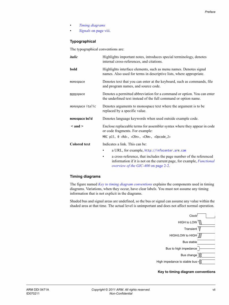
Timing diagrams
The figure named Key to timing diagram conventions explains the components used in timing diagrams. Variations, when they occur, have clear labels. You must not assume any timing information that is not explicit in the diagrams.
Shaded bus and signal areas are undefined, so the bus or signal can assume any value within the shaded area at that time. The actual level is unimportant and does not affect normal operation.
Key to timing diagram conventions
Clock
HIGH to LOW
Transient
HIGH/LOW to HIGH
Bus stable
Bus to high impedance
Bus change
High impedance to stable bus
ARM DDI 0471A Copyright © 2011 ARM. All rights reserved. viiID070211 Non-Confidential
Preface
Signals
The signal conventions are:
Signal level The level of an asserted signal depends on whether the signal is active-HIGH or active-LOW. Asserted means:• HIGH for active-HIGH signals• LOW for active-LOW signals.
Lower-case n At the start or end of a signal name denotes an active-LOW signal.
Additional reading
This section lists publications by ARM and by third parties.
See Infocenter, http://infocenter.arm.com, for access to ARM documentation.
ARM publications
This book contains information that is specific to this product. See the following documents for other relevant information:• ARM® Generic Interrupt Controller Architecture Specification (ARM IHI 0048)• ARM Architecture Reference Manual, ARMv7-A and ARMv7-R edition (ARM DDI 0406)• AMBA® AXI Protocol Specification (ARM IHI 0022).
Other publications
This section lists relevant documents published by third parties:• JEDEC Standard Manufacturer’s Identification Code, JEP106, http://www.jedec.org.
ARM DDI 0471A Copyright © 2011 ARM. All rights reserved. viiiID070211 Non-Confidential

Preface
FeedbackARM welcomes feedback on this product and its documentation.
Feedback on this product
If you have any comments or suggestions about this product, contact your supplier and give:
• The product name.
• The product revision or version.
• An explanation with as much information as you can provide. Include symptoms and diagnostic procedures if appropriate.
Feedback on content
If you have comments on content then send an e-mail to [email protected]. Give:• the title• the number, ARM DDI 0471A• the page numbers to which your comments apply• a concise explanation of your comments.
ARM also welcomes general suggestions for additions and improvements.
ARM DDI 0471A Copyright © 2011 ARM. All rights reserved. ixID070211 Non-Confidential
Chapter 1 Introduction
This chapter introduces the GIC-400. It contains the following sections:• About the GIC-400 on page 1-2• Compliance on page 1-4• Interfaces on page 1-5• Configurable options on page 1-6• Product documentation on page 1-7• Product revisions on page 1-8.
ARM DDI 0471A Copyright © 2011 ARM. All rights reserved. 1-1ID070211 Non-Confidential
Introduction
1.1 About the GIC-400The GIC-400 is a high-performance, area-optimized interrupt controller with an Advanced Microcontroller Bus Architecture (AMBA) Advanced eXtensible Interface (AXI) interface. It detects, manages, and distributes interrupts in System on Chip (SoC) configurations. You can configure the GIC-400 to provide the optimum features, performance, and gate count required for your intended application. For a summary of the configurable features supported, see Configurable options on page 1-6.
With the following software-configurable settings of the GIC-400, interrupts can be:• enabled or disabled• assigned to one of two groups, Group 0 or Group 1• prioritized• signaled to different processors in multiprocessor implementations• either level-sensitive or edge-triggered.
The GIC-400 implements:
• The GIC Security Extensions, that support:— Using Group 0 interrupts as Secure interrupts, and Group 1 interrupts as Non-secure
interrupts.— Optionally, using the FIQ interrupt request to signal Secure interrupts to a connected
processor. The GIC-400 always signals Group 0 interrupts using the IRQ interrupt request.
• The GIC Virtualization Extensions, that provide hardware support for managing virtualized interrupts.
For more information about the GIC Security Extensions and GIC Virtualization Extensions, see the ARM Generic Interrupt Controller Architecture Specification.
You can use the GIC-400 in a multiprocessor system with up to eight processors. The GIC-400 supports systems in which not every processor implements the ARM Security Extensions or the ARM Virtualization Extensions. In such cases, each processor uses only the features it is aware of. For information, see the ARM Generic Interrupt Controller Architecture Specification.
The GIC-400 implements the interrupt types:• 16 Software Generated Interrupts (SGIs)• 6 external Private Peripheral Interrupts (PPIs) for each processor
Note Some PPIs have specific purposes, see Interrupt inputs to the GIC-400 on page 2-8.
• 1 internal PPI for each processor• A configurable number of Shared Peripheral Interrupt (SPIs), see Configurable options
on page 1-6.
The GIC-400 can assert the following signals to indicate pending interrupts to processors:• Physical interrupts:
— nFIQCPU[NUM_CPUS–1:0]— nIRQCPU[NUM_CPUS–1:0].
• Virtual interrupts, see Virtual interrupts in the GIC-400 on page 2-10:— nVFIQCPU[NUM_CPUS–1:0]— nVIRQCPU[NUM_CPUS–1:0].
ARM DDI 0471A Copyright © 2011 ARM. All rights reserved. 1-2ID070211 Non-Confidential

Introduction
Figure 1-1 gives an overview of the GIC-400 in a multiprocessor system. It shows the interrupts that are sent to the GIC-400 from various sources and the key phases of interrupt-related signaling in the SoC.
Figure 1-1 GIC-400 overview
The GIC-400 detects PPIs and SPIs from interrupt input signals. There is one signal for each processor for every PPI interrupt ID. There is only one input signal for each SPI interrupt ID, irrespective of the number of processors in the SoC. SGIs do not have input signals and are generated in the GIC-400 using the AXI programming interface.
Note The GIC-400 does not synchronize any inputs. Therefore, all input signals, including the SPI and PPI inputs, must be synchronous to CLK.
The GIC-400 notifies each processor of the presence of an interrupt or virtual interrupt by using interrupt output signals. There are also interrupt output signals to provide wakeup functionality to a system power controller, see Power management on page 2-12.
Virtual interrupts are created and managed by special software that is executing on each processor that is running virtual machines. Such hypervisors are not part of the GIC-400 architecture but are necessary for the operation of the interrupt controller. For an overview on the hypervisor, see the ARM Generic Interrupt Controller Architecture Specification.
AXI infrastructure
AXI to APBbridgeGPIO
UART DRAM
Flash memory SMC
DMC
GIC-400
Processor
For each processor:FIQ, IRQ, virtual FIQ and virtual IRQ
AXI interface
Programming interface
Peripheral
Interrupts
SGIs
ARM DDI 0471A Copyright © 2011 ARM. All rights reserved. 1-3ID070211 Non-Confidential
Introduction
1.2 ComplianceThe GIC-400 is compliant with:• the AMBA AXI4 protocol, see AMBA AXI Protocol Specification and AXI slave interface
signals on page A-5.• Version 2 of the ARM GIC Architecture Specification, see the ARM Generic Interrupt
Controller Architecture Specification.The GIC-400 implements the GICv2 Security Extensions.
ARM DDI 0471A Copyright © 2011 ARM. All rights reserved. 1-4ID070211 Non-Confidential

Introduction
1.3 InterfacesThe GIC-400 provides an AMBA AXI4 slave interface. With this interface, you can program the Distributor, including generating SGIs, the CPU interfaces, and the virtual CPU interfaces. For information, see AXI slave interface signals on page A-5.
The GIC-400 also supports a set of interrupt signals that it samples to generate PPIs and SPIs. It also generates signals to the wakeup controller and to the processors to indicate that there are valid pending interrupts in the physical and virtual CPU interfaces, see Interrupt signals on page A-4.
ARM DDI 0471A Copyright © 2011 ARM. All rights reserved. 1-5ID070211 Non-Confidential
Introduction
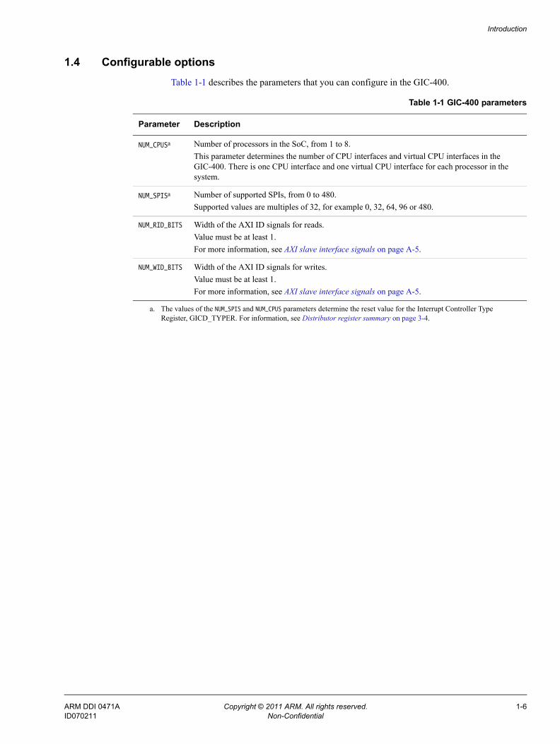
1.4 Configurable optionsTable 1-1 describes the parameters that you can configure in the GIC-400.
Table 1-1 GIC-400 parameters
Parameter Description
NUM_CPUSa Number of processors in the SoC, from 1 to 8.This parameter determines the number of CPU interfaces and virtual CPU interfaces in the GIC-400. There is one CPU interface and one virtual CPU interface for each processor in the system.
NUM_SPISa Number of supported SPIs, from 0 to 480.Supported values are multiples of 32, for example 0, 32, 64, 96 or 480.
NUM_RID_BITS Width of the AXI ID signals for reads.Value must be at least 1.For more information, see AXI slave interface signals on page A-5.
NUM_WID_BITS Width of the AXI ID signals for writes.Value must be at least 1.For more information, see AXI slave interface signals on page A-5.
a. The values of the NUM_SPIS and NUM_CPUS parameters determine the reset value for the Interrupt Controller Type Register, GICD_TYPER. For information, see Distributor register summary on page 3-4.
ARM DDI 0471A Copyright © 2011 ARM. All rights reserved. 1-6ID070211 Non-Confidential

Introduction
1.5 Product documentationThis section describes the GIC-400 documentation, how it relates to the design flow, and the relevant architectural standards and protocols.
Technical Reference Manual The Technical Reference Manual (TRM) describes the functionality and the effects of functional options on the behavior of the GIC-400. It is required at all stages of the design flow. Some behavior described in the TRM might not be relevant because of the way that the GIC-400 is implemented and integrated. If you are programming the GIC-400 then contact:• the implementer to determine the build configuration of the implementation• the integrator to determine the signal configuration of the SoC that you are
using.The TRM complements protocol specifications and relevant external standards. It does not duplicate information from these sources.
ARM DDI 0471A Copyright © 2011 ARM. All rights reserved. 1-7ID070211 Non-Confidential

Introduction
1.6 Product revisionsThis section describes the differences in functionality between the product revisions:
r0p0 First release.
ARM DDI 0471A Copyright © 2011 ARM. All rights reserved. 1-8ID070211 Non-Confidential
Chapter 2 Functional Description
This chapter describes the GIC-400 operation. It contains the following sections:• Functional overview of the GIC-400 on page 2-2• Secure and Non-secure access to the GIC-400 on page 2-7• Interrupt inputs to the GIC-400 on page 2-8• Maintenance interrupts in the GIC-400 on page 2-9• Virtual interrupts in the GIC-400 on page 2-10• Interrupt handling and prioritization in the GIC-400 on page 2-11• Power management on page 2-12• Behavior when the Distributor is disabled on page 2-13.
ARM DDI 0471A Copyright © 2011 ARM. All rights reserved. 2-1ID070211 Non-Confidential
Functional Description
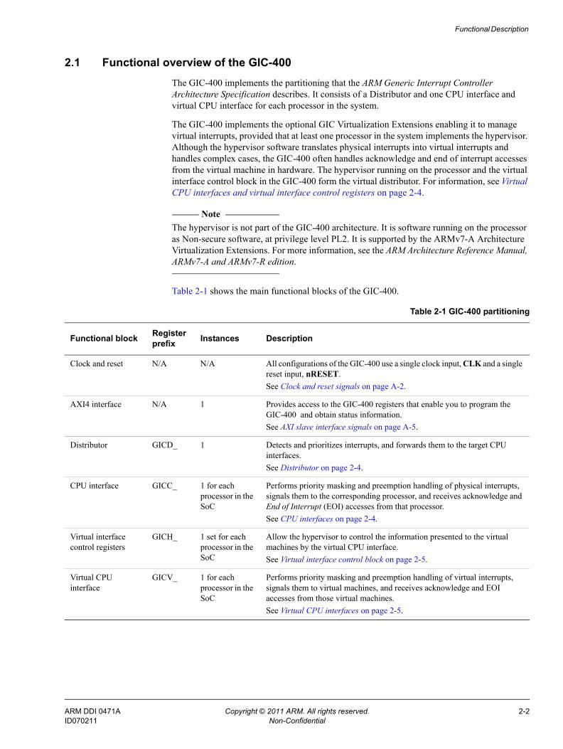
2.1 Functional overview of the GIC-400The GIC-400 implements the partitioning that the ARM Generic Interrupt Controller Architecture Specification describes. It consists of a Distributor and one CPU interface and virtual CPU interface for each processor in the system.
The GIC-400 implements the optional GIC Virtualization Extensions enabling it to manage virtual interrupts, provided that at least one processor in the system implements the hypervisor. Although the hypervisor software translates physical interrupts into virtual interrupts and handles complex cases, the GIC-400 often handles acknowledge and end of interrupt accesses from the virtual machine in hardware. The hypervisor running on the processor and the virtual interface control block in the GIC-400 form the virtual distributor. For information, see Virtual CPU interfaces and virtual interface control registers on page 2-4.
Note The hypervisor is not part of the GIC-400 architecture. It is software running on the processor as Non-secure software, at privilege level PL2. It is supported by the ARMv7-A Architecture Virtualization Extensions. For more information, see the ARM Architecture Reference Manual, ARMv7-A and ARMv7-R edition.
Table 2-1 shows the main functional blocks of the GIC-400.
Table 2-1 GIC-400 partitioning
Functional block Register prefix Instances Description
Clock and reset N/A N/A All configurations of the GIC-400 use a single clock input, CLK and a single reset input, nRESET.See Clock and reset signals on page A-2.
AXI4 interface N/A 1 Provides access to the GIC-400 registers that enable you to program the GIC-400 and obtain status information.See AXI slave interface signals on page A-5.
Distributor GICD_ 1 Detects and prioritizes interrupts, and forwards them to the target CPU interfaces.See Distributor on page 2-4.
CPU interface GICC_ 1 for each processor in the SoC
Performs priority masking and preemption handling of physical interrupts, signals them to the corresponding processor, and receives acknowledge and End of Interrupt (EOI) accesses from that processor.See CPU interfaces on page 2-4.
Virtual interface control registers
GICH_ 1 set for each processor in the SoC
Allow the hypervisor to control the information presented to the virtual machines by the virtual CPU interface.See Virtual interface control block on page 2-5.
Virtual CPU interface
GICV_ 1 for each processor in the SoC
Performs priority masking and preemption handling of virtual interrupts, signals them to virtual machines, and receives acknowledge and EOI accesses from those virtual machines.See Virtual CPU interfaces on page 2-5.
ARM DDI 0471A Copyright © 2011 ARM. All rights reserved. 2-2ID070211 Non-Confidential
Functional Description
2.1.1 Clock and reset
All configurations of the GIC-400 use a single clock input, CLK and a single reset input, nRESET. For information, see Clock and reset signals on page A-2.
Note Clock and reset signals apply to all interfaces on the GIC-400 and all interfaces must be synchronous to this clock. Therefore, synchronizer cells might be required for certain inputs.
2.1.2 AXI4 interface
The GIC-400 uses an AMBA AXI4 slave interface.
There are no separate AXI clock and reset signals in the GIC-400. All interfaces are synchronous to the master clock input.
Note In many cases, the GIC-400 might be compatible with an AXI3 master. However, the AXI4 protocol does not support the AXI3 features of locked transactions and write-interleaving and clarifies the meaning of the AWCACHE and the ARCACHE signals. Therefore, to ensure that the GIC-400 is operating correctly, you must configure any AXI3 masters not to issue locked transactions or interleave write data. You must also check that all interconnects obey the restrictions set out by the AXI4 definitions of AWCACHE and the ARCACHE for the relevant transaction type, which is typically expected to be Device Bufferable. For information on legacy considerations in AXI4, see the AMBA AXI Protocol Specification.
The AWUSER and ARUSER signals are specific to the GIC-400. They indicate to the GIC-400 which processor is performing a request. Identifying the requestor is necessary to determine to which CPU interface or virtual CPU interface an AXI access should be directed. Furthermore, this is needed for some Distributor register accesses, such as the GICD_SGIR, as well.
The format of the AWUSER and ARUSER signals is a binary number from 0 to NUM_CPUS-1, inclusive. The only strict requirement to generate the AWUSER and ARUSER signals is that the chosen numbering scheme must represent a consistent mapping between the processors and the range of legal encodings. Processors can discover their ID that the GIC-400 uses by reading from the Interrupt Processor Targets Register0, GICD_ITARGETSR0.
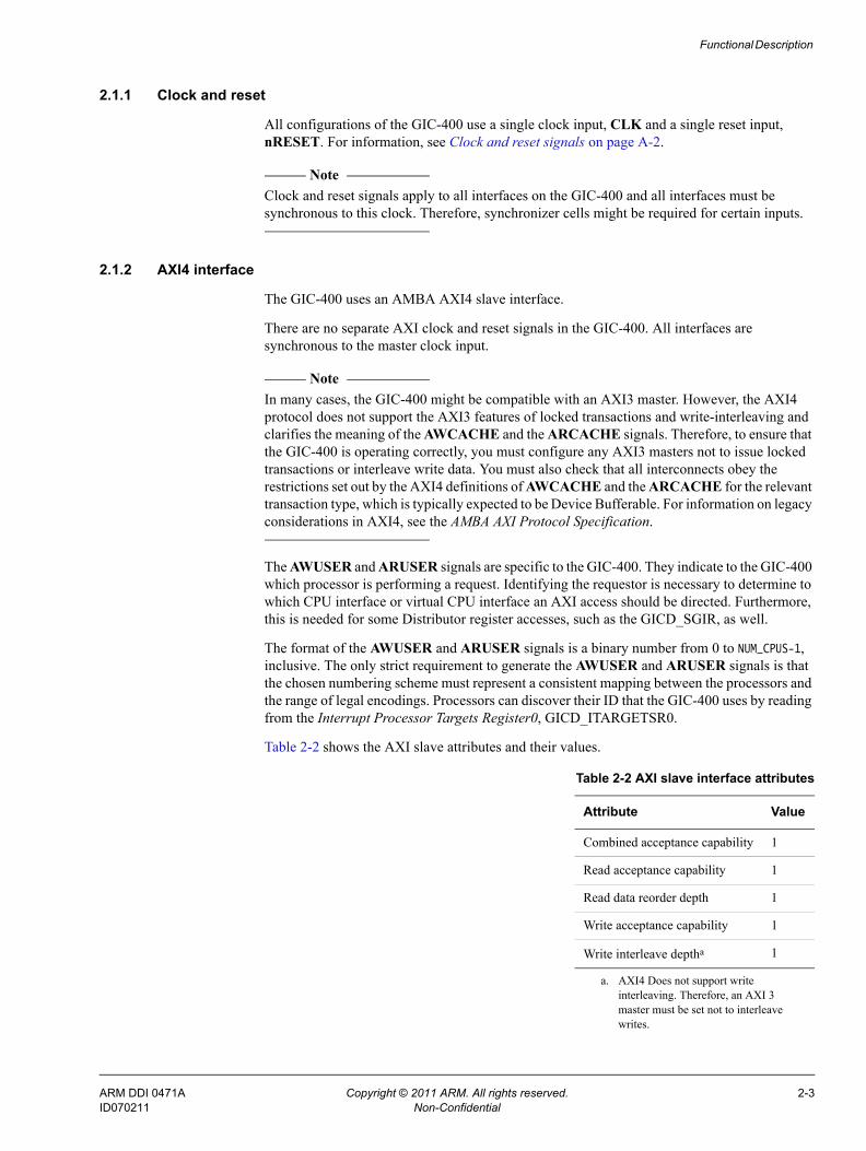
Table 2-2 shows the AXI slave attributes and their values.
Table 2-2 AXI slave interface attributes
Attribute Value
Combined acceptance capability 1
Read acceptance capability 1
Read data reorder depth 1
Write acceptance capability 1
Write interleave deptha
a. AXI4 Does not support write interleaving. Therefore, an AXI 3 master must be set not to interleave writes.
1
ARM DDI 0471A Copyright © 2011 ARM. All rights reserved. 2-3ID070211 Non-Confidential
Functional Description
2.1.3 Distributor
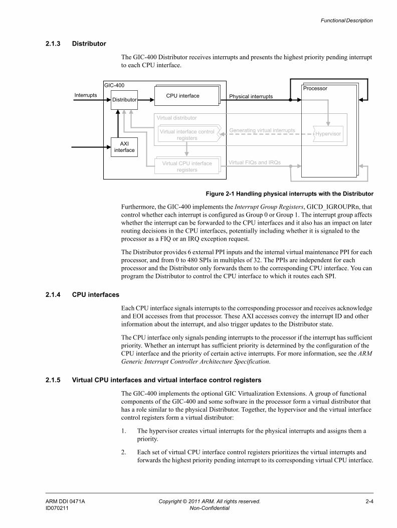
The GIC-400 Distributor receives interrupts and presents the highest priority pending interrupt to each CPU interface.
Figure 2-1 Handling physical interrupts with the Distributor
Furthermore, the GIC-400 implements the Interrupt Group Registers, GICD_IGROUPRn, that control whether each interrupt is configured as Group 0 or Group 1. The interrupt group affects whether the interrupt can be forwarded to the CPU interfaces and it also has an impact on later routing decisions in the CPU interfaces, potentially including whether it is signaled to the processor as a FIQ or an IRQ exception request.
The Distributor provides 6 external PPI inputs and the internal virtual maintenance PPI for each processor, and from 0 to 480 SPIs in multiples of 32. The PPIs are independent for each processor and the Distributor only forwards them to the corresponding CPU interface. You can program the Distributor to control the CPU interface to which it routes each SPI.
2.1.4 CPU interfaces
Each CPU interface signals interrupts to the corresponding processor and receives acknowledge and EOI accesses from that processor. These AXI accesses convey the interrupt ID and other information about the interrupt, and also trigger updates to the Distributor state.
The CPU interface only signals pending interrupts to the processor if the interrupt has sufficient priority. Whether an interrupt has sufficient priority is determined by the configuration of the CPU interface and the priority of certain active interrupts. For more information, see the ARM Generic Interrupt Controller Architecture Specification.
2.1.5 Virtual CPU interfaces and virtual interface control registers
The GIC-400 implements the optional GIC Virtualization Extensions. A group of functional components of the GIC-400 and some software in the processor form a virtual distributor that has a role similar to the physical Distributor. Together, the hypervisor and the virtual interface control registers form a virtual distributor:
1. The hypervisor creates virtual interrupts for the physical interrupts and assigns them a priority.
2. Each set of virtual CPU interface control registers prioritizes the virtual interrupts and forwards the highest priority pending interrupt to its corresponding virtual CPU interface.
GIC-400
Physical interruptsCPU interface
AXI interface
DistributorInterrupts
Processor
Generating virtual interrupts
Virtual FIQs and IRQs
Virtual interface control registers
Virtual CPU interfaceregisters
Virtual distributor
Hypervisor
ARM DDI 0471A Copyright © 2011 ARM. All rights reserved. 2-4ID070211 Non-Confidential

Functional Description
The hypervisor supports virtualization also by using address translation tables to trap accesses that the virtual machines make to the virtual distributor. The hypervisor determines the effect of these accesses and might typically update the virtual interface control registers as a result.
Figure 2-2 shows how the virtual distributor is implemented partly in the GIC-400, partly in the processor and how it interacts with the Distributor and the virtual CPU interfaces in the GIC-400. The GIC-400 implements the virtual interface control registers, namely the GICH_ registers and the processor implements the hypervisor.
Figure 2-2 Handling virtual interrupts with the virtual distributor
Virtual interface control block
The GIC-400 implements the virtual interface control block with all the management registers and with four List registers. The List registers, GICH_LR0 - GICH_LR3, are a subset of the virtual interface control registers and define the active and pending virtual interrupts for the virtual CPU interface. The management registers, for example the Virtual Machine Control Register, GICH_VMCR, and Active Priorities Register, GICH_APR, enable the hypervisor to manage other aspects of the corresponding virtual CPU interface, and permit it to save and restore state when switching between virtual machines.
Virtual CPU interfaces
The virtual CPU interface registers are similar to the CPU interface registers. However, the virtual CPU interfaces receive information from the virtual interface control registers, which are managed by the hypervisor, rather than from the Distributor.
After receiving a physical interrupt or otherwise, if the hypervisor needs to signal a virtual interrupt to the current virtual machine, it typically updates the virtual interface control registers. These registers, specifically the List registers, GICH_LRn, hold a list of the virtual interrupts destined for the current virtual machine. The signaling, acknowledgement and EOI steps of the virtual interrupt processing can usually be handled in hardware by the virtual CPU interface. Certain cases might require hypervisor intervention, for example if there are more virtual interrupts than can be stored in the List registers. The virtual interface control registers control when an internal PPI, known as the virtual maintenance interrupt, is generated. This virtual maintenance interrupt, PPI ID 25, is designed to notify the hypervisor of events that it must handle.
The address translation tables for the processor are normally configured so that accesses to the CPU interface by a virtual machine are directed to the virtual CPU interface. This ensures that the virtualization of the CPU interface is transparent to the virtual machine.
GIC-400
Physical interruptsCPU interface
AXI interface
DistributorInterrupts
Processor
Generating virtual interrupts
Virtual FIQs and IRQs
Virtual interface control registers
Hypervisor
Virtual CPU interfaceregisters
Virtual distributor
ARM DDI 0471A Copyright © 2011 ARM. All rights reserved. 2-5ID070211 Non-Confidential
Functional Description
Hypervisor
The hypervisor is not part of the GIC-400 but it is crucial for its operation. It is software executing on each processor that is running virtual machines:
• It is responsible for translating physical interrupts to virtual interrupts and managing all virtual interrupts by using the virtual interface control registers.
• It can also configure the virtual maintenance interrupt to signal situations when it must manage the virtual interrupts.
• It typically sets the stage 2 Non-secure address translation tables so that the virtual machines access the virtual CPU interfaces instead of the physical interfaces.
• The hypervisor is responsible for virtualizing accesses from the virtual machines to the Distributor, typically by trapping the accesses and handling them in software.
For information, see the ARM Architecture Reference Manual, ARMv7-A and ARMv7-R edition.
Note ARM processors support the use of a hypervisor when they implement the ARM Virtualization Extensions. For information on extension versions and their dependencies on other ARM processor extensions, see the ARM Architecture Reference Manual, ARMv7-A and ARMv7-R edition.
ARM DDI 0471A Copyright © 2011 ARM. All rights reserved. 2-6ID070211 Non-Confidential

Functional Description
2.2 Secure and Non-secure access to the GIC-400For information about Secure and Non-secure accesses to the GIC, and the implications for processors that do not implement the ARM Security Extensions, see the ARM Generic Interrupt Controller Architecture Specification.
ARM DDI 0471A Copyright © 2011 ARM. All rights reserved. 2-7ID070211 Non-Confidential

Functional Description
2.3 Interrupt inputs to the GIC-400This section describes the different types of interrupt that the GIC-400 handles. See also Behavior when the Distributor is disabled on page 2-13.
2.3.1 SGIs
SGIs are generated by writing to the Software Generated Interrupt Register, GICD_SGIR. Each CPU interface can generate a maximum of 16 SGIs, ID0-ID15, for each target processor.
2.3.2 PPIs
A PPI is an interrupt that is specific to a single processor. All PPI signals are active-LOW level-sensitive. Table 2-3 shows the PPIs that are available for each processor.
2.3.3 SPIs
SPIs are triggered by events generated on associated interrupt input lines. The GIC-400 can support up to 480 SPIs corresponding to the external IRQS[479:0] signal. The number of SPIs available depends on the implemented configuration of the GIC-400. The permitted values are 0-480, in steps of 32. SPIs start at ID32.You can configure whether each SPI is edge-triggered on a rising edge or is active-HIGH level-sensitive.
Note All signals, including SPIs, must be synchronous to the clock in the GIC-400. Therefore, any interrupt signals from an asynchronous source must be synchronized before they are connected to the GIC-400.
2.3.4 Lockable SPIs (LSPIs)
The GIC-400 supports 31 LSPIs, as it is indicated by the LSPI field in the Interrupt Controller Type Register, GICD_TYPER. For more information, see the ARM Generic Interrupt Controller Architecture Specification.
Table 2-3 PPI types
Interrupt ID Source Description
31 Legacy IRQ signal When the power management bypass functionality is enabled in a CPU interface, the legacy IRQ signal is driven on its nIRQCPU output. See Power management on page 2-12.This interrupt input also behaves like a normal PPI input at all times.
30 Non-secure physical timer This is the event generated by the Non-secure physical timer.
29 Secure physical timer This is the event generated by the Secure physical timer.
28 Legacy FIQ signal When the power management bypass functionality is enabled in a CPU interface, the legacy FIQ signal is driven on its nFIQCPU output. See Power management on page 2-12. This interrupt input also behaves like a normal PPI input at all times.
27 Virtual timer This is the event generated by the virtual timer.
26 Hypervisor timer This is the event generated by the physical timer in Hyp mode.
25 Virtual maintenance interrupt This is a configurable event generated by the corresponding virtual CPU interface to indicate a situation that might require hypervisor action.
ARM DDI 0471A Copyright © 2011 ARM. All rights reserved. 2-8ID070211 Non-Confidential

Functional Description
2.4 Maintenance interrupts in the GIC-400See PPIs on page 2-8 and the ARM Generic Interrupt Controller Architecture Specification.
ARM DDI 0471A Copyright © 2011 ARM. All rights reserved. 2-9ID070211 Non-Confidential

Functional Description
2.5 Virtual interrupts in the GIC-400The GIC-400 supports interrupt virtualization to assert virtual interrupts to virtual machines using the virtual CPU interfaces. Virtual interrupts can be created only if the processor has a hypervisor to manage the virtual machines in the SoC and perform the translation from the physical to virtual interrupt. For information, see the ARM Generic Interrupt Controller Architecture Specification.
ARM DDI 0471A Copyright © 2011 ARM. All rights reserved. 2-10ID070211 Non-Confidential

Functional Description
2.6 Interrupt handling and prioritization in the GIC-400In the GIC-400, the Distributor arbitrates physical interrupts and the virtual distributor arbitrates virtual interrupts according to the same principles.
The GIC-400 implements the interrupt handling and prioritization of the ARM Generic Interrupt Controller Architecture Specification. The following IMPLEMENTATION DEFINED properties are particular to the GIC-400:
• The GIC-400 implements 32 priority levels in Secure state and 16 priority states in Non-secure state.
• If two or more interrupts have the same priority level, the arbitration depends on the type of the interrupts:PPI, SPI The Distributor issues the interrupt with the lowest ID.SGI The Distributor issues the SGI with the lowest ID. In multiprocessor systems,
if a priority level conflict remains, the Distributor issues the SGI that was generated by the processor with the lowest CPUID. Therefore, when a priority level conflict occurs, an SGI request from processor 0 is given preference over other SGIs with that same ID.
• Writing to the Interrupt Priority Registers, GICD_IPRIORITYR, does not affect the priority of an active interrupt.
ARM DDI 0471A Copyright © 2011 ARM. All rights reserved. 2-11ID070211 Non-Confidential
Functional Description
2.7 Power managementThe GIC-400 implements the bypass functionality as specified by the GIC architecture specification. This means that if a CPU interface processor output, such as one bit of nFIQCPU, is disabled, the GIC-400 is bypassed unless the bypass functionality is itself disabled. Bypassing means that the GIC-400 drives the corresponding legacy input on the processor interrupt output, for instance one bit of nLEGACYFIQ driving the same bit of nFIQCPU. This is the behavior from reset.
The bypass functionality can be disabled so that when the CPU interface processor output is disabled, the output signal is deasserted rather than bypassed. This is typically used when powering down a processor to ensure that when the CPU interface is disabled, the legacy interrupt inputs do not wake the processor. Bypassing can be disabled using the CPU Interface Control Register, GICC_CTLR.
The GIC-400 supports wakeup events in systems that require power management. It signals these wakeup events using nIRQOUT and nFIQOUT, which ignore the CPU interface enable bits, unlike the processor output signals, nIRQCPU and nFIQCPU. As a result, the wakeup outputs are always enabled and so do not support bypass or bypass disable functionality.
For information about power management, wakeup signals and their relation to the processor outputs, see the ARM Generic Interrupt Controller Architecture Specification.
ARM DDI 0471A Copyright © 2011 ARM. All rights reserved. 2-12ID070211 Non-Confidential
Functional Description
2.8 Behavior when the Distributor is disabledIf at least one of the GICD_CTLR.EnableGrp0 or GICD_CTLR.EnableGrp1 bits is 0:
• an edge-triggered interrupt signal cannot set the interrupt to the pending state if the interrupt is in a disabled group
• SGIs in a disabled group cannot be set pending using the GICD_SGIR.
If either, but not both, of the GICD_CTLR.EnableGrp0 and GICD_CTLR.EnableGrp1 bits is set to 1, and the highest priority pending interrupt is in the disabled group, the Distributor does not forward any pending interrupts to the CPU interfaces. This applies in the following cases:
• GICD_CTLR.EnableGrp0 set to 0 and GICD_CTLR.EnableGrp1 set to 1, and the highest priority pending interrupt is in Group 0
• GICD_CTLR.EnableGrp0 set to 1 and GICD_CTLR.EnableGrp1 set to 0, and the highest priority pending interrupt is in Group 1.
This means that, in cases where there are Group 1 interrupts with a higher priority than some Group 0 interrupts, it is possible for Non-secure software to deny service to Secure software, by clearing the GICD_CTLR.EnableGrp1 bit. To prevent this, ARM strongly recommends that all Group 0 interrupts are assigned a higher priority than all Group 1 interrupts. In addition, to prevent Secure software from denying service to Non-secure software, Secure software must ensure that when GICD_CTLR.EnableGrp1 is set to 1, either GICD_CTLR.EnableGrp0 is also set to 1, or there are no pending Group 0 interrupts.
For more information, see the ARM Generic Interrupt Controller Architecture Specification.
ARM DDI 0471A Copyright © 2011 ARM. All rights reserved. 2-13ID070211 Non-Confidential

Chapter 3 Programmers Model
This chapter describes the GIC-400 registers and provides information about programming the device. It contains the following sections:• About the GIC-400 programmers model on page 3-2• GIC-400 register map on page 3-3• Distributor register summary on page 3-4• Distributor register descriptions on page 3-6• CPU interface register summary on page 3-10• CPU interface register descriptions on page 3-11• GIC virtual interface control register summary on page 3-12• GIC virtual interface control register descriptions on page 3-13• GIC virtual CPU interface register summary on page 3-14• GIC virtual CPU interface register descriptions on page 3-15.
ARM DDI 0471A Copyright © 2011 ARM. All rights reserved. 3-1ID070211 Non-Confidential
Programmers Model
3.1 About the GIC-400 programmers modelThe GIC-400 implements the following registers:
• Distributor registers, see Distributor register summary on page 3-4
• CPU interface registers, see CPU interface register summary on page 3-10
• GIC virtual interface control registers, see GIC virtual interface control register summary on page 3-12
• GIC virtual CPU interface registers, see GIC virtual CPU interface register summary on page 3-14.
The following information applies to the GIC-400 registers:
• The base address of the GIC-400 is not fixed, and can be different for a particular system implementation. The offset of each register from the base address is fixed.
• Access to reserved or unused address locations is RAZ/WI (Read-as-Zero, Writes Ignored).
• Unless otherwise stated in the accompanying text:— do not modify reserved register bits— ignore reserved register bits on reads— all register bits are reset to 0 by a system or power-on reset.
• The bus width of the GIC-400 is 32 bits. The ARM Generic Interrupt Controller Architecture Specification defines the permitted sizes of access. When byte access is permitted, halfword access is also permitted. Byte or halfword accesses to registers that do not permit that access size return a SLVERR response if they are unsuccessful.
• The GIC-400 only supports data in little-endian format.
• This chapter describes the access types as follows:RAZ/WI Read-as-Zero, Writes IgnoredRO Read onlyRW Read and writeWO Write only.
ARM DDI 0471A Copyright © 2011 ARM. All rights reserved. 3-2ID070211 Non-Confidential
Programmers Model
3.2 GIC-400 register mapAll of the GIC-400 registers have short names. In these names, the first three characters are GIC, and the fourth character indicates the functional block of the GIC-400:GICD_ DistributorGICC_ CPU interfacesGICH_ Virtual interface control blocksGICV_ Virtual CPU interfaces.
The GIC-400 provides the following register aliases for the virtual interface control block:
• An alias that provides access to the virtual CPU interface of the accessing processor using a single base address for all processors. This base address is at offset 0x4000.
• Aliases that permit any virtual CPU interface to be accessed explicitly from any other processor, using a different base address for each processor. The starting base address is at offset 0x5000, with address bits [11:9] as the CPU ID decode.
The GIC-400 registers are memory-mapped. Table 3-1 lists the address ranges.
3.2.1 GIC-400 register access and banking
For information on the register access and banking scheme, see the ARM Generic Interrupt Controller Architecture Specification. The key characteristics of the scheme are:
• Some registers, such as the Distributor Control Register, GICD_CTLR, and the CPU Interface Control Register, GICC_CTLR, are security Banked. This provides separate Secure and Non-secure copies of the registers. Secure AXI accesses access Secure registers, and Non-secure AXI accesses access Non-secure registers. Furthermore, when the GIC-400 is implemented as part of a multiprocessor system, registers associated with PPIs or SGIs are Banked to provide a separate copy for each connected processor.
• Some registers, such as the Interrupt Group Registers, GICD_IGROUPRn, are only accessible by Secure accesses.
• Non-secure accesses to registers or parts of a register that are only accessible to Secure accesses are RAZ/WI for that part.
For more information, see the ARM Generic Interrupt Controller Architecture Specification.
Table 3-1 GIC-400 memory map
Address range GIC-400 functional block
0x0000-0x0FFF Reserved
0x1000-0x1FFF Distributor
0x2000-0x3FFF CPU interfaces
0x4000-0x4FFF Virtual interface control block, for the processor that is performing the access
0x5000-0x5FFF Virtual interface control block, for the processor selected by address bits [11:9]
0x5000-0x51FF0x5200-0x53FF...0x5E00-0x5FFF
Alias for Processor 0Alias for Processor 1...Alias for Processor 7
0x6000-0x7FFF Virtual CPU interfaces
ARM DDI 0471A Copyright © 2011 ARM. All rights reserved. 3-3ID070211 Non-Confidential
Programmers Model
3.3 Distributor register summaryTable 3-2 lists the Distributor registers in base offset order and provides a reference to the register description that either this book or the ARM Generic Interrupt Controller Architecture Specification describes.
Offsets that are not shown are reserved.
Table 3-2 Distributor register summary
Offset Namea Type Reset Full nameb
0x000 GICD_CTLR RW 0x00000000c Distributor Control Register
0x004 GICD_TYPER RO Configuration-dependentd Interrupt Controller Type Register
0x008 GICD_IIDR RO 0x0200043B Distributor Implementer Identification Register, GICD_IIDR on page 3-6
0x080-0x0BC GICD_IGROUPRn RW 0x00000000 Interrupt Group Registerse
0x100 GICD_ISENABLERn RWf SGIs and PPIs: 0x0000FFFFg Interrupt Set-Enable Registers
0x104-0x13C SPIs: 0x00000000
0x180 GICD_ICENABLERn RWf 0x0000FFFFg Interrupt Clear-Enable Registers
0x184-0x1BC 0x00000000
0x200-0x23C GICD_ISPENDRn RW 0x00000000 Interrupt Set-Pending Registers
0x280-0x2BC GICD_ICPENDRn RW 0x00000000 Interrupt Clear-Pending Registers
0x300-0x33C GICD_ISACTIVERn RW 0x00000000 Interrupt Set-Active Registers
0x380-0x3BC GICD_ICACTIVERn RW 0x00000000 Interrupt Clear-Active Registers
0x400-0x5FC GICD_IPRIORITYRn RW 0x00000000 Interrupt Priority Registers
0x800-0x81C GICD_ITARGETSRn ROh - Interrupt Processor Targets Registersi
0x820-0x9FC RW 0x00000000
0xC00 GICD_ICFGRn RO SGIs: 0xAAAAAAAA Interrupt Configuration Registers, GICD_ICFGRn on page 3-6
0xC04 RO PPIs: 0x55540000
0xC08-0xC7C RWj SPIs: 0x55555555
0xD00 GICD_PPISR RO 0x00000000 Private Peripheral Interrupt Status Register, GICD_PPISR on page 3-7
0xD04-0xD3C GICD_SPISRn RO 0x00000000 Shared Peripheral Interrupt Status Registers, GICD_SPISRn on page 3-7
0xF00 GICD_SGIR WO - Software Generated Interrupt Register
0xF10-0xF1C GICD_CPENDSGIRn RW 0x00000000 SGI Clear-Pending Registers
0xF20-0xF2C GICD_SPENDSGIRn RW 0x00000000 SGI Set-Pending Registers
0xFD0 GICD_PIDR4 RO 0x00000004 Peripheral ID 4 Register
0xFD4 GICD_PIDR5 RO 0x00000000 Peripheral ID 5 Register
0xFD8 GICD_PIDR6 RO 0x00000000 Peripheral ID 6 Register
ARM DDI 0471A Copyright © 2011 ARM. All rights reserved. 3-4ID070211 Non-Confidential

Programmers Model
0xFDC GICD_PIDR7 RO 0x00000000 Peripheral ID 7 Register
0xFE0 GICD_PIDR0 RO 0x00000090 Peripheral ID 0 Register
0xFE4 GICD_PIDR1 RO 0x000000B4 Peripheral ID 1 Register
0xFE8 GICD_PIDR2 RO 0x0000002B Peripheral ID 2 Register
0xFEC GICD_PIDR3 RO 0x00000000 Peripheral ID 3 Register
0xFF0 GICD_CIDR0 RO 0x0000000D Component ID 0 Register
0xFF4 GICD_CIDR1 RO 0x000000F0 Component ID 1 Register
0xFF8 GICD_CIDR2 RO 0x00000005 Component ID 2 Register
0xFFC GICD_CIDR3 RO 0x000000B1 Component ID 3 Register
a. n corresponds to the number of a CPU interface.b. For the description of registers that are not specific to the GIC-400, see the ARM Generic Interrupt Controller Architecture Specification.c. You cannot modify the EnableGrp0 bit if CFGSDISABLE is set.d. The reset value depends on the configuration of the GIC-400. The configuration-dependent values are two fields of the Interrupt Controller
Type Register, GICD_TYPER:LSPI, bits [15:11] 11111, see Lockable SPIs (LSPIs) on page 2-8.SecurityExtn, bit [10] 1CPUNumber, bits [7:5] Has the value of (NUM_CPUS-1), see Configurable options on page 1-6.ITLinesNumber, bits [4:0] Has the value of NUM_SPIS/32, see Configurable options on page 1-6.
ITLinesNumber expresses that the GIC supports at most (ITLinesNumber+1)*32 interrupts, that is, the potentially implemented interrupt IDs are 0 to ((ITLinesNumber+1)*32-1). This information can then be used by software to restrict the range of interrupts that are accessed during interrupt discovery. In the GIC-400, all interrupts are implemented except for the unused PPIs, IDs 16-24.For NUM_SPIS=0, ITLinesNumber=0, which gives a maximum of 32 interrupts, with the ID range 0-31. So for this example, IDs 0-15 (all SGIs) and 25-31 (some PPIs) are implemented.For NUM_SPIS=64, ITLinesNumber=2, which gives a maximum of 96 interrupts, IDs 0-95. IDs 16-24 are unimplemented in this example as well.
For information, see the ARM Generic Interrupt Controller Architecture Specification. e. This register is only accessible from a Secure access.f. Writes to bits corresponding to the SGIs are ignored.g. The reset value for the register that contains the SGI and PPI interrupts is 0x0000FFFF because SGIs are always enabled. However, SGIs are
Group 0 on reset, so the reset value for Non-secure reads is 0x00000000.h. The registers that contain the SGI and PPI interrupts are read-only and the value is the CPU number of the current access. It is encoded in
an 8-bit one-hot field, for each implemented interrupt, and zero for interrupts that are not implemented. For more information on CPU targets field bit values, see the ARM Generic Interrupt Controller Architecture Specification.
i. In uniprocessor systems, these registers are RAZ/WI. For information, see the ARM Generic Interrupt Controller Architecture Specification.j. The even bits of this register are RO, see Interrupt Configuration Registers, GICD_ICFGRn on page 3-6.
Table 3-2 Distributor register summary (continued)
Offset Namea Type Reset Full nameb
ARM DDI 0471A Copyright © 2011 ARM. All rights reserved. 3-5ID070211 Non-Confidential
Programmers Model
3.4 Distributor register descriptionsThis section only describes the Distributor registers whose implementation is specific to the GIC-400. The ARM Generic Interrupt Controller Architecture Specification describes all the other registers.
3.4.1 Distributor Implementer Identification Register, GICD_IIDR
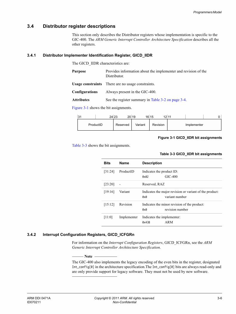
The GICD_IIDR characteristics are:
Purpose Provides information about the implementer and revision of the Distributor.
Usage constraints There are no usage constraints.
Configurations Always present in the GIC-400.
Attributes See the register summary in Table 3-2 on page 3-4.
Figure 3-1 shows the bit assignments.
Figure 3-1 GICD_IIDR bit assignments
Table 3-3 shows the bit assignments.
3.4.2 Interrupt Configuration Registers, GICD_ICFGRn
For information on the Interrupt Configuration Registers, GICD_ICFGRn, see the ARM Generic Interrupt Controller Architecture Specification.
Note The GIC-400 also implements the legacy encoding of the even bits in the register, designated Int_config[0] in the architecture specification.The Int_config[0] bits are always read-only and are only provide support for legacy software. They must not be used by new software.
Reserved RevisionVariant ImplementerProductID
31 024 1123 1220 19 16 15
Table 3-3 GICD_IIDR bit assignments
Bits Name Description
[31:24] ProductID Indicates the product ID: 0x02 GIC-400
[23:20] - Reserved, RAZ
[19:16] Variant Indicates the major revision or variant of the product: 0x0 variant number
[15:12] Revision Indicates the minor revision of the product: 0x0 revision number
[11:0] Implementer Indicates the implementer: 0x43B ARM
ARM DDI 0471A Copyright © 2011 ARM. All rights reserved. 3-6ID070211 Non-Confidential
Programmers Model
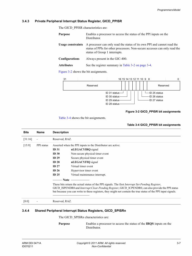
3.4.3 Private Peripheral Interrupt Status Register, GICD_PPISR
The GICD_PPISR characteristics are:
Purpose Enables a processor to access the status of the PPI inputs on the Distributor.
Usage constraints A processor can only read the status of its own PPI and cannot read the status of PPIs for other processors. Non-secure accesses can only read the status of Group 1 interrupts.
Configurations Always present in the GIC-400.
Attributes See the register summary in Table 3-2 on page 3-4.
Figure 3-2 shows the bit assignments.
Figure 3-2 GICD_PPISR bit assignments
Table 3-4 shows the bit assignments.
3.4.4 Shared Peripheral Interrupt Status Registers, GICD_SPISRn
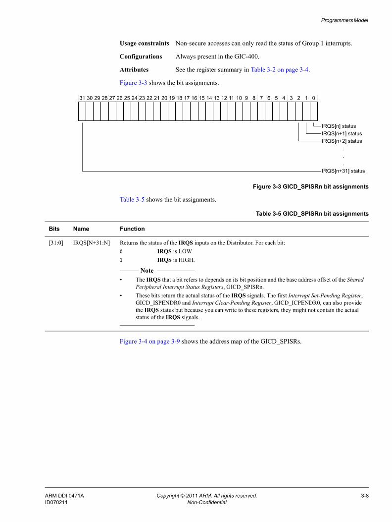
The GICD_SPISRn characteristics are:
Purpose Enables a processor to access the status of the IRQS inputs on the Distributor.
Reserved
31 16 15 14 13 12 11 10 9 8 0
Reserved
ID 31 statusID 30 statusID 29 statusID 28 status
ID 27 statusID 26 statusID 25 status
Table 3-4 GICD_PPISR bit assignments
Bits Name Description
[31:16] - Reserved, RAZ.
[15:9] PPI status Asserted when the PPI inputs to the Distributor are active.ID 31 nLEGACYIRQ signalID 30 Non-secure physical timer eventID 29 Secure physical timer eventID 28 nLEGACYFIQ signalID 27 Virtual timer eventID 26 Hypervisor timer eventID 25 Virtual maintenance interrupt.
Note These bits return the actual status of the PPI signals. The first Interrupt Set-Pending Register, GICD_ISPENDR0 and Interrupt Clear-Pending Register, GICD_ICPENDR0, can also provide the PPI status but because you can write to these registers, they might not contain the true status of the PPI input signals.
[8:0] - Reserved, RAZ.
ARM DDI 0471A Copyright © 2011 ARM. All rights reserved. 3-7ID070211 Non-Confidential
Programmers Model
Usage constraints Non-secure accesses can only read the status of Group 1 interrupts.
Configurations Always present in the GIC-400.
Attributes See the register summary in Table 3-2 on page 3-4.
Figure 3-3 shows the bit assignments.
Figure 3-3 GICD_SPISRn bit assignments
Table 3-5 shows the bit assignments.
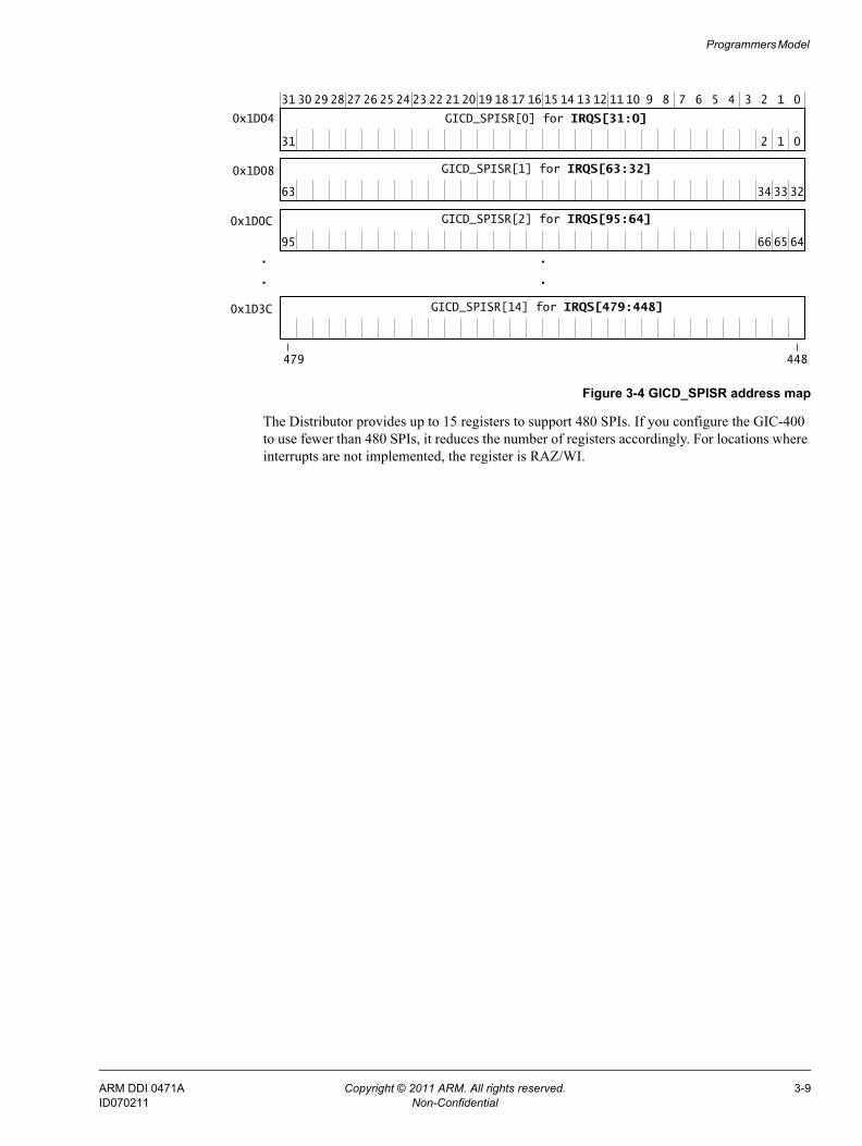
Figure 3-4 on page 3-9 shows the address map of the GICD_SPISRs.
31 30 29 28 27 26 25 24 23 22 21 20 19 18 17 16 15 14 13 12 11 10 9 8 7 6 5 4 3 2 1 0
IRQS[n] statusIRQS[n+1] statusIRQS[n+2] status
IRQS[n+31] status
.
.
.
Table 3-5 GICD_SPISRn bit assignments
Bits Name Function
[31:0] IRQS[N+31:N] Returns the status of the IRQS inputs on the Distributor. For each bit:0 IRQS is LOW1 IRQS is HIGH.
Note • The IRQS that a bit refers to depends on its bit position and the base address offset of the Shared
Peripheral Interrupt Status Registers, GICD_SPISRn.• These bits return the actual status of the IRQS signals. The first Interrupt Set-Pending Register,
GICD_ISPENDR0 and Interrupt Clear-Pending Register, GICD_ICPENDR0, can also provide the IRQS status but because you can write to these registers, they might not contain the actual status of the IRQS signals.
ARM DDI 0471A Copyright © 2011 ARM. All rights reserved. 3-8ID070211 Non-Confidential
Programmers Model
Figure 3-4 GICD_SPISR address map
The Distributor provides up to 15 registers to support 480 SPIs. If you configure the GIC-400 to use fewer than 480 SPIs, it reduces the number of registers accordingly. For locations where interrupts are not implemented, the register is RAZ/WI.
31 30 29 28 27 26 25 24 23 22 21 20 19 18 17 16 15 14 13 12 11 10 9 8 7 6 5 4 3 2 1 0
GICD_SPISR[0] for IRQS[31:0]
031 12
GICD_SPISR[1] for IRQS[63:32]
95
GICD_SPISR[2] for IRQS[95:64]
646566
GICD_SPISR[14] for IRQS[479:448]
.
.
448
.
.
0x1D08
0x1D0C
0x1D3C
479
3263 3334
0x1D04
ARM DDI 0471A Copyright © 2011 ARM. All rights reserved. 3-9ID070211 Non-Confidential
Programmers Model
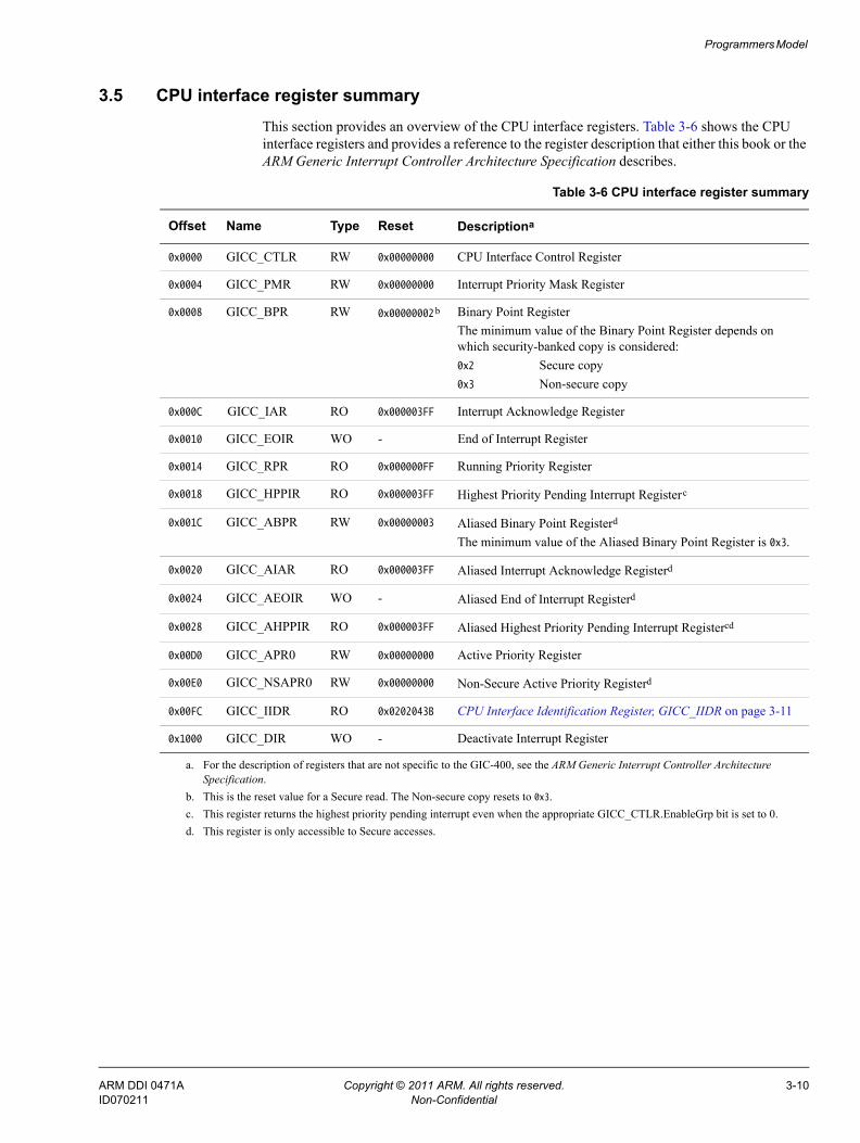
3.5 CPU interface register summaryThis section provides an overview of the CPU interface registers. Table 3-6 shows the CPU interface registers and provides a reference to the register description that either this book or the ARM Generic Interrupt Controller Architecture Specification describes.
Table 3-6 CPU interface register summary
Offset Name Type Reset Descriptiona
0x0000 GICC_CTLR RW 0x00000000 CPU Interface Control Register
0x0004 GICC_PMR RW 0x00000000 Interrupt Priority Mask Register
0x0008 GICC_BPR RW 0x00000002b Binary Point RegisterThe minimum value of the Binary Point Register depends on which security-banked copy is considered:0x2 Secure copy0x3 Non-secure copy
0x000C GICC_IAR RO 0x000003FF Interrupt Acknowledge Register
0x0010 GICC_EOIR WO - End of Interrupt Register
0x0014 GICC_RPR RO 0x000000FF Running Priority Register
0x0018 GICC_HPPIR RO 0x000003FF Highest Priority Pending Interrupt Registerc
0x001C GICC_ABPR RW 0x00000003 Aliased Binary Point Registerd
The minimum value of the Aliased Binary Point Register is 0x3.
0x0020 GICC_AIAR RO 0x000003FF Aliased Interrupt Acknowledge Registerd
0x0024 GICC_AEOIR WO - Aliased End of Interrupt Registerd
0x0028 GICC_AHPPIR RO 0x000003FF Aliased Highest Priority Pending Interrupt Registercd
0x00D0 GICC_APR0 RW 0x00000000 Active Priority Register
0x00E0 GICC_NSAPR0 RW 0x00000000 Non-Secure Active Priority Registerd
0x00FC GICC_IIDR RO 0x0202043B CPU Interface Identification Register, GICC_IIDR on page 3-11
0x1000 GICC_DIR WO - Deactivate Interrupt Register
a. For the description of registers that are not specific to the GIC-400, see the ARM Generic Interrupt Controller Architecture Specification.
b. This is the reset value for a Secure read. The Non-secure copy resets to 0x3.c. This register returns the highest priority pending interrupt even when the appropriate GICC_CTLR.EnableGrp bit is set to 0.d. This register is only accessible to Secure accesses.
ARM DDI 0471A Copyright © 2011 ARM. All rights reserved. 3-10ID070211 Non-Confidential
Programmers Model
3.6 CPU interface register descriptionsThis section only describes the CPU interface register whose implementation is specific to the GIC-400. The ARM Generic Interrupt Controller Architecture Specification describes all the other registers.
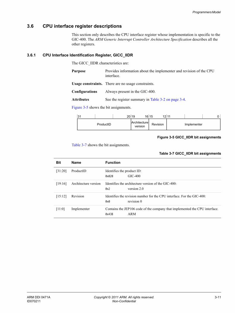
3.6.1 CPU Interface Identification Register, GICC_IIDR
The GICC_IIDR characteristics are:
Purpose Provides information about the implementer and revision of the CPU interface.
Usage constraints. There are no usage constraints.
Configurations Always present in the GIC-400.
Attributes See the register summary in Table 3-2 on page 3-4.
Figure 3-5 shows the bit assignments.
Figure 3-5 GICC_IIDR bit assignments
Table 3-7 shows the bit assignments.
31 0
Revision Implementer
20 11
ProductID
19 121516
Architectureversion
Table 3-7 GICC_IIDR bit assignments
Bit Name Function
[31:20] ProductID Identifies the product ID:0x020 GIC-400
[19:16] Architecture version Identifies the architecture version of the GIC-400:0x2 version 2.0
[15:12] Revision Identifies the revision number for the CPU interface. For the GIC-400:0x0 revision 0
[11:0] Implementer Contains the JEP106 code of the company that implemented the CPU interface.0x43B ARM
ARM DDI 0471A Copyright © 2011 ARM. All rights reserved. 3-11ID070211 Non-Confidential
Programmers Model
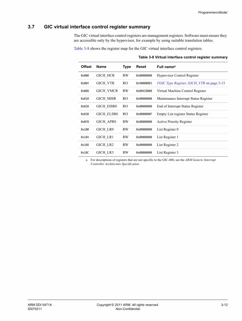
3.7 GIC virtual interface control register summaryThe GIC virtual interface control registers are management registers. Software must ensure they are accessible only by the hypervisor, for example by using suitable translation tables.
Table 3-8 shows the register map for the GIC virtual interface control registers.
Table 3-8 Virtual interface control register summary
Offset Name Type Reset Full namea
a. For descriptions of registers that are not specific to the GIC-400, see the ARM Generic Interrupt Controller Architecture Specification.
0x000 GICH_HCR RW 0x00000000 Hypervisor Control Register
0x004 GICH_VTR RO 0x90000003 VGIC Type Register, GICH_VTR on page 3-13
0x008 GICH_VMCR RW 0x004C0000 Virtual Machine Control Register
0x010 GICH_MISR RO 0x00000000 Maintenance Interrupt Status Register
0x020 GICH_EISR0 RO 0x00000000 End of Interrupt Status Register
0x030 GICH_ELSR0 RO 0x0000000F Empty List register Status Register
0x0F0 GICH_APR0 RW 0x00000000 Active Priority Register
0x100 GICH_LR0 RW 0x00000000 List Register 0
0x104 GICH_LR1 RW 0x00000000 List Register 1
0x108 GICH_LR2 RW 0x00000000 List Register 2
0x10C GICH_LR3 RW 0x00000000 List Register 3
ARM DDI 0471A Copyright © 2011 ARM. All rights reserved. 3-12ID070211 Non-Confidential
Programmers Model
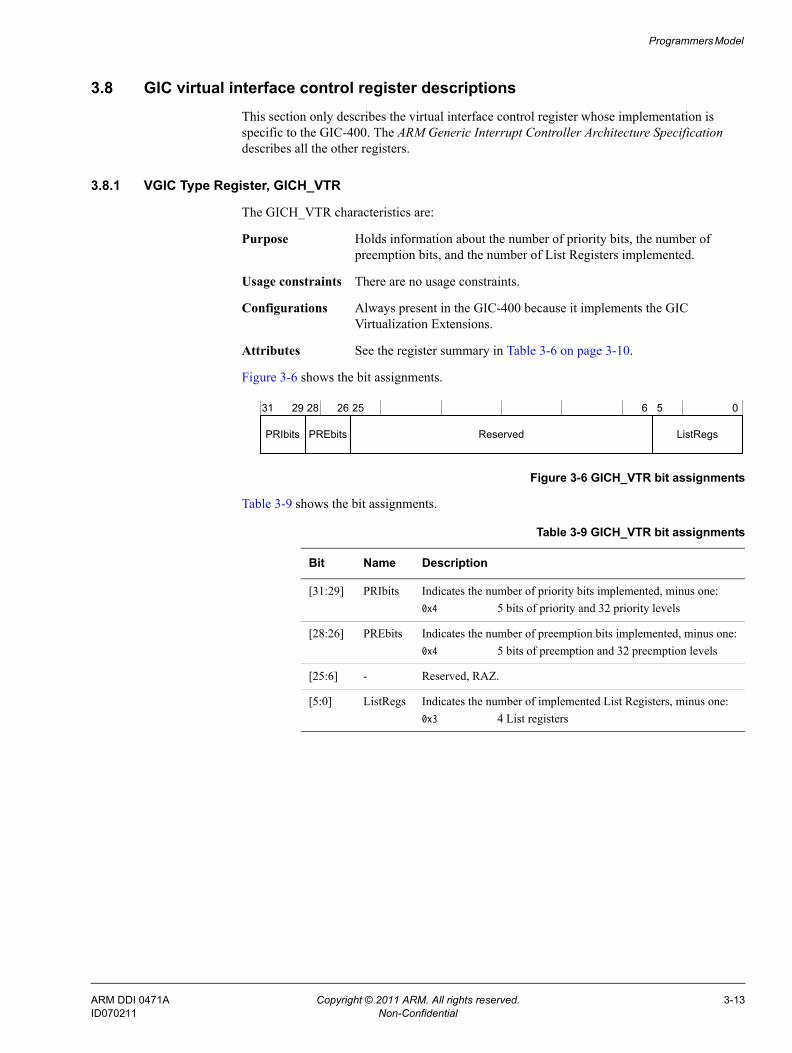
3.8 GIC virtual interface control register descriptionsThis section only describes the virtual interface control register whose implementation is specific to the GIC-400. The ARM Generic Interrupt Controller Architecture Specification describes all the other registers.
3.8.1 VGIC Type Register, GICH_VTR
The GICH_VTR characteristics are:
Purpose Holds information about the number of priority bits, the number of preemption bits, and the number of List Registers implemented.
Usage constraints There are no usage constraints.
Configurations Always present in the GIC-400 because it implements the GIC Virtualization Extensions.
Attributes See the register summary in Table 3-6 on page 3-10.
Figure 3-6 shows the bit assignments.
Figure 3-6 GICH_VTR bit assignments
Table 3-9 shows the bit assignments.
PRIbits
31 29 28 26 25 6 5 0
PREbits Reserved ListRegs
Table 3-9 GICH_VTR bit assignments
Bit Name Description
[31:29] PRIbits Indicates the number of priority bits implemented, minus one:0x4 5 bits of priority and 32 priority levels
[28:26] PREbits Indicates the number of preemption bits implemented, minus one:0x4 5 bits of preemption and 32 preemption levels
[25:6] - Reserved, RAZ.
[5:0] ListRegs Indicates the number of implemented List Registers, minus one:0x3 4 List registers
ARM DDI 0471A Copyright © 2011 ARM. All rights reserved. 3-13ID070211 Non-Confidential

Programmers Model
3.9 GIC virtual CPU interface register summaryTable 3-10 shows the register map for the GIC virtual CPU interface in the GIC-400.
Registers that this table does not describe are RAZ/WI.
Table 3-10 GIC virtual CPU interface register summary
Offset Name Type Reset Full namea
0x0000 GICV_CTLR RW 0x00000000 Virtual Machine Control Register
0x0004 GICV_PMR RW 0x00000000 VM Priority Mask Register
0x0008 GICV_BPR RW 0x00000002 VM Binary Point Register
0x000C GICV_IAR RO 0x000003FF VM Interrupt Acknowledge Register
0x0010 GICV_EOIR WO - VM End of Interrupt Register
0x0014 GICV_RPR RO 0x000000FF VM Running Priority Register
0x0018 GICV_HPPIR RO 0x000003FF VM Highest Priority Pending Interrupt Registerb
0x001C GICV_ABPR RW 0x00000003 VM Aliased Binary Point Register
0x0020 GICV_AIAR RO 0x000003FF VM Aliased Interrupt Acknowledge Register
0x0024 GICV_AEOIR WO - VM Aliased End of Interrupt Register
0x0028 GICV_AHPPIR RO 0x000003FF VM Aliased Highest Priority Pending Interrupt Registerb
0x00D0 GICV_APR0 RW 0x00000000 VM Active Priority Register
0x00FC GICV_IIDR RO 0x0202043B VM CPU Interface Identification Register, GICV_IIDR on page 3-15
0x1000 GICV_DIR WO - VM Deactivate Interrupt Register
a. For descriptions of registers that are not specific to the GIC-400, see the ARM Generic Interrupt Controller Architecture Specification.
b. This register returns the highest priority pending interrupt even when the appropriate GICV_CTLR.EnableGrp bit is set to 0.
ARM DDI 0471A Copyright © 2011 ARM. All rights reserved. 3-14ID070211 Non-Confidential
Programmers Model
3.10 GIC virtual CPU interface register descriptionsThis section only describes the virtual CPU interface registers whose implementation is specific to the GIC-400. The ARM Generic Interrupt Controller Architecture Specification describes all the other registers.
3.10.1 VM CPU Interface Identification Register, GICV_IIDR
The GICV_IIDR characteristics are:
Purpose Provides information about the implementer and revision of the virtual CPU interface.
Usage constraints There are no usage constraints.
Configurations Always present in the GIC-400 because it implements the GIC Virtualization Extensions.
Attributes See the register summary in Table 3-6 on page 3-10.
The bit assignments for the GICV_IIDR are identical to the corresponding register in the Physical CPU interface, see CPU Interface Identification Register, GICC_IIDR on page 3-11.
ARM DDI 0471A Copyright © 2011 ARM. All rights reserved. 3-15ID070211 Non-Confidential
Appendix A Signal Descriptions
This appendix describes the signals that the GIC-400 provides. It contains the following sections:• Clock and reset signals on page A-2• Configuration signal on page A-3• Interrupt signals on page A-4• AXI slave interface signals on page A-5.
ARM DDI 0471A Copyright © 2011 ARM. All rights reserved. A-1ID070211 Non-Confidential

Signal Descriptions
A.1 Clock and reset signalsTable A-1 shows the clock and reset signals.
Note The GIC-400 does not synchronize any inputs, so all input signals, including the SPI and PPI inputs, must be synchronous to CLK.
Table A-1 Clock and reset signals
Signal Direction Type Description
CLK Input Clock source Common clock signal for AXI and other interfaces.
nRESET Input Reset source Reset for the GIC-400.
DFTRSTDISABLE Input DFT control logic Disables the external reset input for test mode.
DFTSE Input DFT control logic Scan enable. Disables clock gates for test mode.
ARM DDI 0471A Copyright © 2011 ARM. All rights reserved. A-2ID070211 Non-Confidential
Signal Descriptions
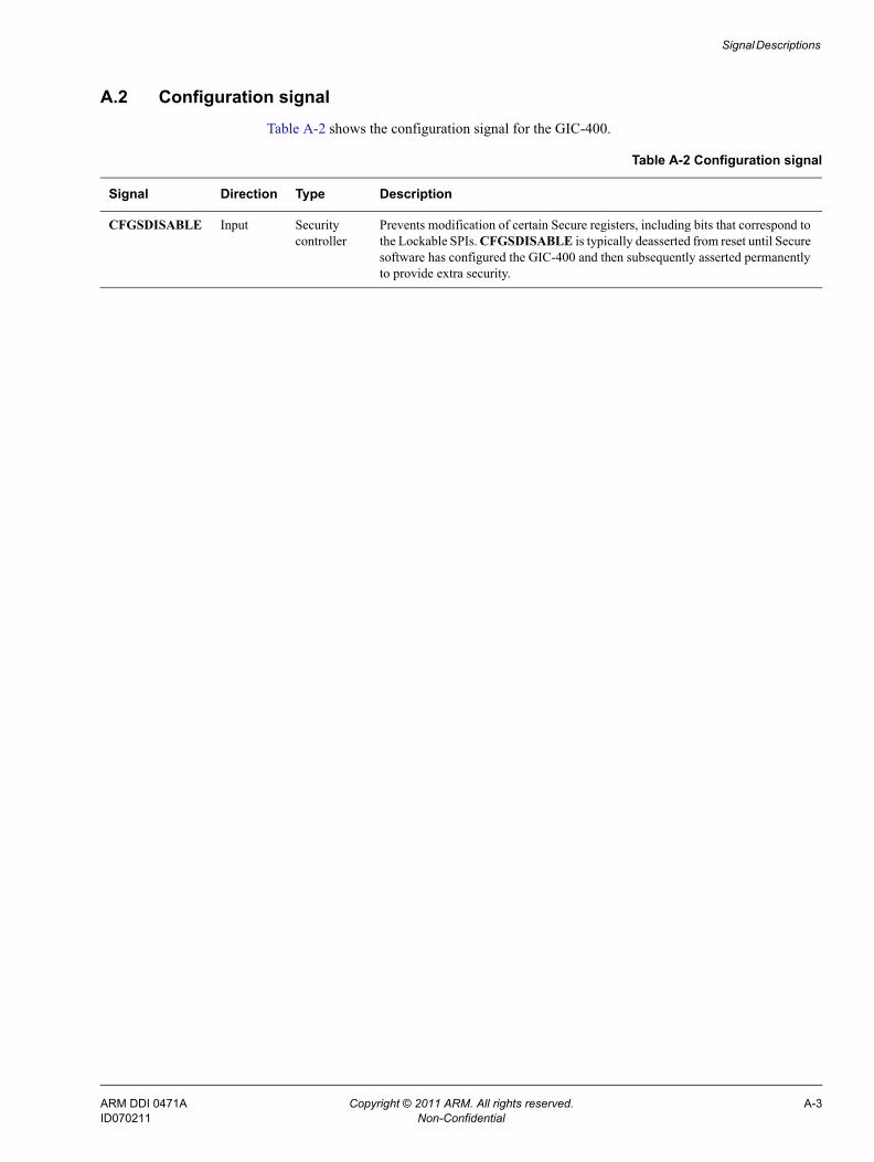
A.2 Configuration signalTable A-2 shows the configuration signal for the GIC-400.
Table A-2 Configuration signal
Signal Direction Type Description
CFGSDISABLE Input Security controller
Prevents modification of certain Secure registers, including bits that correspond to the Lockable SPIs. CFGSDISABLE is typically deasserted from reset until Secure software has configured the GIC-400 and then subsequently asserted permanently to provide extra security.
ARM DDI 0471A Copyright © 2011 ARM. All rights reserved. A-3ID070211 Non-Confidential
Signal Descriptions
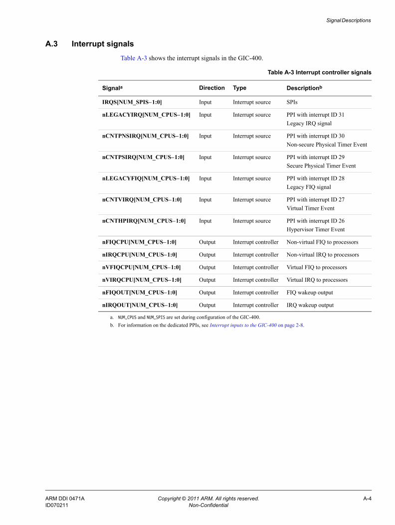
A.3 Interrupt signalsTable A-3 shows the interrupt signals in the GIC-400.
Table A-3 Interrupt controller signals
Signala Direction Type Descriptionb
IRQS[NUM_SPIS–1:0] Input Interrupt source SPIs
nLEGACYIRQ[NUM_CPUS–1:0] Input Interrupt source PPI with interrupt ID 31Legacy IRQ signal
nCNTPNSIRQ[NUM_CPUS–1:0] Input Interrupt source PPI with interrupt ID 30Non-secure Physical Timer Event
nCNTPSIRQ[NUM_CPUS–1:0] Input Interrupt source PPI with interrupt ID 29Secure Physical Timer Event
nLEGACYFIQ[NUM_CPUS–1:0] Input Interrupt source PPI with interrupt ID 28Legacy FIQ signal
nCNTVIRQ[NUM_CPUS–1:0] Input Interrupt source PPI with interrupt ID 27Virtual Timer Event
nCNTHPIRQ[NUM_CPUS–1:0] Input Interrupt source PPI with interrupt ID 26Hypervisor Timer Event
nFIQCPU[NUM_CPUS–1:0] Output Interrupt controller Non-virtual FIQ to processors
nIRQCPU[NUM_CPUS–1:0] Output Interrupt controller Non-virtual IRQ to processors
nVFIQCPU[NUM_CPUS–1:0] Output Interrupt controller Virtual FIQ to processors
nVIRQCPU[NUM_CPUS–1:0] Output Interrupt controller Virtual IRQ to processors
nFIQOUT[NUM_CPUS–1:0] Output Interrupt controller FIQ wakeup output
nIRQOUT[NUM_CPUS–1:0] Output Interrupt controller IRQ wakeup output
a. NUM_CPUS and NUM_SPIS are set during configuration of the GIC-400.b. For information on the dedicated PPIs, see Interrupt inputs to the GIC-400 on page 2-8.
ARM DDI 0471A Copyright © 2011 ARM. All rights reserved. A-4ID070211 Non-Confidential
Signal Descriptions
A.4 AXI slave interface signalsThe GIC-400 provides a 32-bit wide AXI4 slave interface. For information, see the AMBA AXI Protocol Specification.
AXI4 signals that are not implemented in the GIC-400 are not shown in the table.
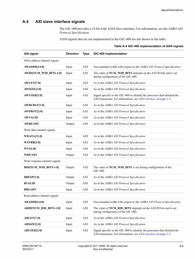
Table A-4 GIC-400 implementation of AXI4 signals
AXI signal Direction Type GIC-400 implementation
Write address channel signals
AWADDR[14:0] Input AXI Non-standard width with respect to the AMBA AXI Protocol Specification.
AWID[NUM_WID_BITS-1:0] Input AXI The value of NUM_WID_BITS depends on the AXI ID bits and is set during configuration of the GIC-400.
AWLEN[7:0] Input AXI As in the AMBA AXI Protocol Specification.
AWSIZE[2:0] Input AXI As in the AMBA AXI Protocol Specification.
AWUSER[2:0] Input AXI Signal specific to the GIC-400 to identify the processor that initiated the AXI transaction. For information, see AXI4 interface on page 2-3.
AWBURST[1:0] Input AXI As in the AMBA AXI Protocol Specification
AWPROT[2:0] Input AXI As in the AMBA AXI Protocol Specification
AWVALID Input AXI As in the AMBA AXI Protocol Specification
AWREADY Output AXI As in the AMBA AXI Protocol Specification
Write data channel signals
WDATA[31:0] Input AXI As in the AMBA AXI Protocol Specification
WSTRB[3:0] Input AXI As in the AMBA AXI Protocol Specification
WVALID Input AXI As in the AMBA AXI Protocol Specification
WREADY Output AXI As in the AMBA AXI Protocol Specification
Write response channel signals
BID[NUM_WID_BITS-1:0] Output AXI The value of NUM_WID_BITS is set during configuration of the GIC-400.
BRESP[1:0] Output AXI As in the AMBA AXI Protocol Specification
BVALID Output AXI As in the AMBA AXI Protocol Specification
BREADY Input AXI As in the AMBA AXI Protocol Specification
Read address channel signals
ARADDR[14:0] Input AXI Non-standard width with respect to the AMBA AXI Protocol Specification
ARID[NUM_RID_BITS-1:0] Input AXI The value of NUM_RID_BITS depends on the AXI ID bits and is set during configuration of the GIC-400.
ARLEN[7:0] Input AXI As in the AMBA AXI Protocol Specification
ARSIZE[2:0] Input AXI As in the AMBA AXI Protocol Specification.
ARUSER[2:0] Input AXI Signal specific to the GIC-400 to identify the processor that initiated the AXI transaction. For information, see AXI4 interface on page 2-3.
ARM DDI 0471A Copyright © 2011 ARM. All rights reserved. A-5ID070211 Non-Confidential

Signal Descriptions
ARBURST[1:0] Input AXI As in the AMBA AXI Protocol Specification
ARPROT[2:0] Input AXI As in the AMBA AXI Protocol Specification
ARVALID Input AXI As in the AMBA AXI Protocol Specification
ARREADY Output AXI As in the AMBA AXI Protocol Specification
Read data channel signals
RID[NUM_RID_BITS-1:0] Output AXI The value of NUM_RID_BITS is set during configuration of the GIC-400.
RDATA[31:0] Output AXI As in the AMBA AXI Protocol Specification
RRESP[1:0] Output AXI As in the AMBA AXI Protocol Specification
RLAST Output AXI As in the AMBA AXI Protocol Specification
RVALID Output AXI As in the AMBA AXI Protocol Specification
RREADY Input AXI As in the AMBA AXI Protocol Specification
Table A-4 GIC-400 implementation of AXI4 signals (continued)
AXI signal Direction Type GIC-400 implementation
ARM DDI 0471A Copyright © 2011 ARM. All rights reserved. A-6ID070211 Non-Confidential
Appendix B Interrupt Signaling
This appendix describes how the GIC-400 signals interrupts to a processor. It contains the following sections:• Interrupt signaling in the GIC-400 with physical interrupts only on page B-2• Interrupt signaling in the GIC-400 with virtual interrupts on page B-4.
ARM DDI 0471A Copyright © 2011 ARM. All rights reserved. B-1ID070211 Non-Confidential
Interrupt Signaling
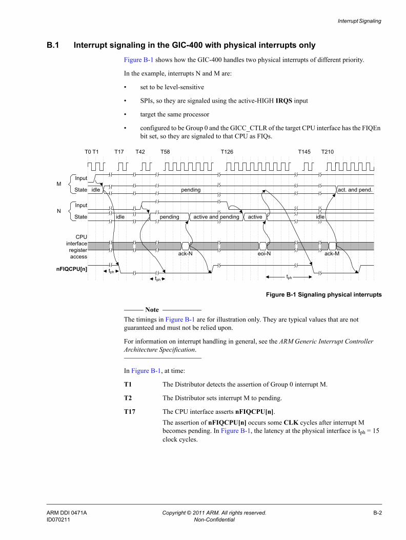
B.1 Interrupt signaling in the GIC-400 with physical interrupts onlyFigure B-1 shows how the GIC-400 handles two physical interrupts of different priority.
In the example, interrupts N and M are:
• set to be level-sensitive
• SPIs, so they are signaled using the active-HIGH IRQS input
• target the same processor
• configured to be Group 0 and the GICC_CTLR of the target CPU interface has the FIQEn bit set, so they are signaled to that CPU as FIQs.
Figure B-1 Signaling physical interrupts
Note The timings in Figure B-1 are for illustration only. They are typical values that are not guaranteed and must not be relied upon.
For information on interrupt handling in general, see the ARM Generic Interrupt Controller Architecture Specification.
In Figure B-1, at time:
T1 The Distributor detects the assertion of Group 0 interrupt M.
T2 The Distributor sets interrupt M to pending.
T17 The CPU interface asserts nFIQCPU[n].The assertion of nFIQCPU[n] occurs some CLK cycles after interrupt M becomes pending. In Figure B-1, the latency at the physical interface is tph = 15 clock cycles.
idle
nFIQCPU[n]
State
T1
pending
idle
T17 T42 T58
Input
active and pending
M
State
InputN
CPUinterface registeraccess
idle
tph tph
pending act. and pend.
ack-N eoi-N ack-M
T145
tph
T210T0 T126
active
ARM DDI 0471A Copyright © 2011 ARM. All rights reserved. B-2ID070211 Non-Confidential

Interrupt Signaling
Note The Distributor takes several cycles to calculate the highest priority pending
interrupt. If an interrupt becomes pending while the calculation is in progress, it only affects the results of the next calculation. This means that the interrupt latency might vary. Therefore, while tph is typically 12 cycles, it might often be between 10 and 20 cycles.
T42 The Distributor detects the assertion of a higher priority Group 0 interrupt, N.
T43 The Distributor replaces interrupt M with interrupt N as the highest priority pending interrupt and sets N to pending.
T58 tph clock cycles after interrupt N became pending, the CPU interface asserts nFIQCPU[n]. The state of nFIQCPU[n] is unchanged because nFIQCPU[n] was asserted at T17.The CPU interface updates the InterruptID field in the GICC_IAR, to contain the ID value for interrupt N.
T61 The processor reads the GICC_IAR, acknowledging the highest priority pending interrupt, N.The Distributor sets interrupt N to active and pending.
T61-T131 The processor services interrupt N.
T64 3 clock cycles after interrupt N has been acknowledged, the CPU interface deasserts nFIQCPU[n].
T126 The peripheral deasserts interrupt N.
T128 The pending state is removed from N.
T131 The processor writes to the End of Interrupt Register, GICC_EOIR, with the ID of interrupt N and the Distributor deactivates interrupt N.
T146 tph clock cycles after GICC_EOIR was written to for N, the Distributor forwards the new highest priority pending interrupt, M, to the CPU interface, which asserts nFIQCPU[n].
T211 The processor reads the GICC_IAR, acknowledging the highest priority pending interrupt, M, and the Distributor sets interrupt M to active and pending.
T214 3 clock cycles after interrupt M has been acknowledged, the CPU interface deasserts nFIQCPU[n].
ARM DDI 0471A Copyright © 2011 ARM. All rights reserved. B-3ID070211 Non-Confidential
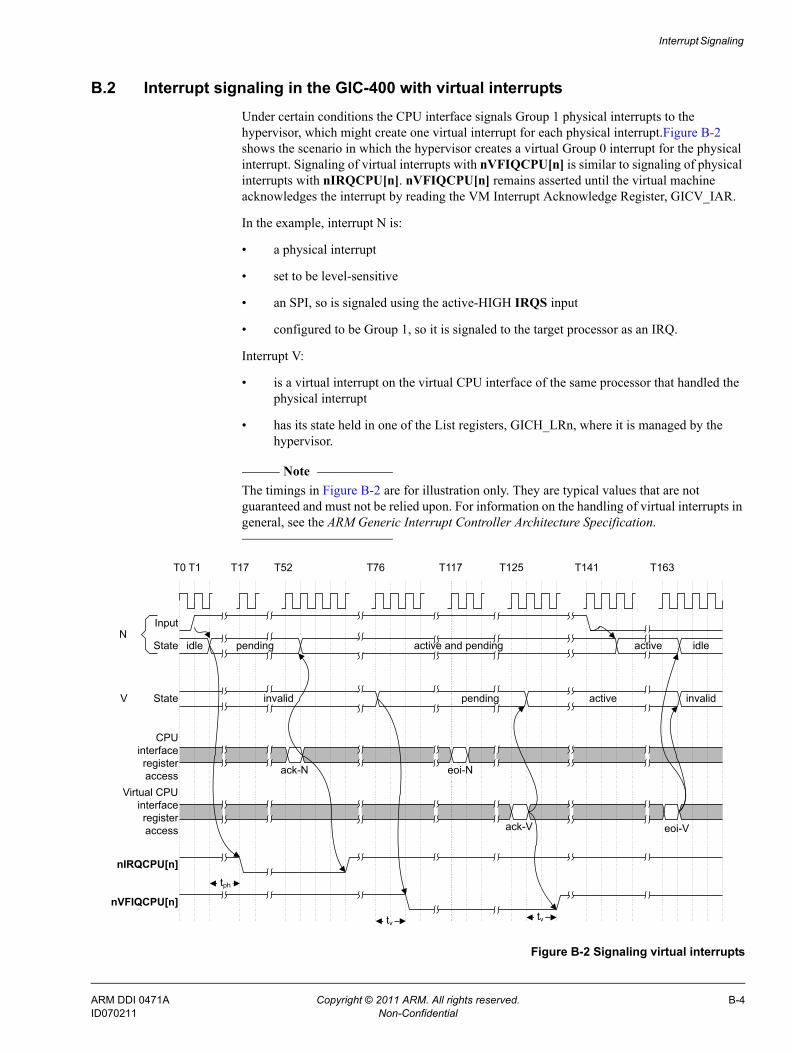
Interrupt Signaling
B.2 Interrupt signaling in the GIC-400 with virtual interruptsUnder certain conditions the CPU interface signals Group 1 physical interrupts to the hypervisor, which might create one virtual interrupt for each physical interrupt.Figure B-2 shows the scenario in which the hypervisor creates a virtual Group 0 interrupt for the physical interrupt. Signaling of virtual interrupts with nVFIQCPU[n] is similar to signaling of physical interrupts with nIRQCPU[n]. nVFIQCPU[n] remains asserted until the virtual machine acknowledges the interrupt by reading the VM Interrupt Acknowledge Register, GICV_IAR.
In the example, interrupt N is:
• a physical interrupt
• set to be level-sensitive
• an SPI, so is signaled using the active-HIGH IRQS input
• configured to be Group 1, so it is signaled to the target processor as an IRQ.
Interrupt V:
• is a virtual interrupt on the virtual CPU interface of the same processor that handled the physical interrupt
• has its state held in one of the List registers, GICH_LRn, where it is managed by the hypervisor.
Note The timings in Figure B-2 are for illustration only. They are typical values that are not guaranteed and must not be relied upon. For information on the handling of virtual interrupts in general, see the ARM Generic Interrupt Controller Architecture Specification.
Figure B-2 Signaling virtual interrupts
nVFIQCPU[n]
State
T1
pendinginvalid
idle
T17 T52 T125
Input
T0
active
N
State
CPUinterface registeraccess
invalid
ack-N
Virtual CPUinterface registeraccess ack-V eoi-V
nIRQCPU[n]tph
pending active and pending idle
T117
tv
V
eoi-N
T141 T163
active
tv
T76
ARM DDI 0471A Copyright © 2011 ARM. All rights reserved. B-4ID070211 Non-Confidential

Interrupt Signaling
In Figure B-2 on page B-4, at time:
T1 The Distributor detects the assertion of Group 1 interrupt N.
T2 The Distributor sets interrupt N to pending.
T17 The Distributor updates the InterruptID field in the GICC_IAR, to contain the ID value for N and the CPU interface asserts nIRQCPU[n].The assertion of nIRQCPU[n] occurs some CLK cycles after interrupt N becomes pending. In Figure B-2 on page B-4, the latency at the physical CPU interface, tph, is 15 clock cycles.
T53 The hypervisor reads the Non-secure GICC_IAR to acknowledge the highest priority pending physical interrupt, N. This changes the state of interrupt N to active and pending.
T56 3 clock cycles after N becomes active and pending, the CPU interface deasserts nIRQCPU[n].
T76 The hypervisor writes to an empty List register, which creates interrupt V, a pending Group 0 hardware virtual interrupt with the PhysicalID field that contains the ID of interrupt N.
T78 The virtual CPU interface asserts nVFIQCPU[n].The assertion of nVFIQCPU[n] occurs some CLK cycles after interrupt V becomes pending. In Figure B-2 on page B-4, the latency at the virtual CPU interface, tv, is 2 clock cycles.
T118 The hypervisor writes to the End of Interrupt Register, GICC_EOIR, with the ID of interrupt N.
Note Since GICC_CTLR.EOImodeNS had been set to 1, the end-of-interrupt only
results in a priority drop so that physical interrupts with a lower priority than N’s can be signaled to the processor. The state of interrupt N remains unchanged.
T126 The virtual machine reads the GICC_IAR, acknowledging the highest priority pending Group 0 virtual interrupt, V.Interrupt V becomes active.
T127 - T163 The virtual machine services interrupt V.
T128 tv after V has been acknowledged, the virtual CPU interface deasserts nVFIQCPU[n].
T141 When the virtual machine has dealt with the event that had caused the interrupt, the peripheral deasserts the interrupt signal.
T143 After the deassertion of input N is detected, the pending state is removed from N.
T164 The virtual machine writes to the VM End of Interrupt Register, GICV_EOIR, with the ID of interrupt V.This causes the deactivation of interrupt V and, because V is a hardware virtual interrupt, also the deactivation of the associated physical interrupt, N.
ARM DDI 0471A Copyright © 2011 ARM. All rights reserved. B-5ID070211 Non-Confidential

ARM DDI 0471A Copyright © 2011 ARM. All rights reserved. C-1ID070211 Non-Confidential
Appendix C Revisions
This appendix describes the technical changes between released issues of this book.
Table C-1 Issue A
Change Location Affects
First release - -