coremdio apb v2 - fpga & soc | fpga & soc | products v2.0 handbook 3 table of contents...
TRANSCRIPT
CoreMDIO_APB v2.0 Handbook

2 CoreMDIO_APB v2.0 Handbook
Revision History Date Revision Change August 2015 1 Initial release
Confidentiality Status This is a non-confidential document.

CoreMDIO_APB v2.0 Handbook 3
Table of Contents
Preface ...........................................................................................................................................5 About this Document .................................................................................................................................................. 5 Intended Audience ...................................................................................................................................................... 5 References................................................................................................................................................................... 5
Introduction ..................................................................................................................................6 Overview ...................................................................................................................................................................... 6 Key Features ............................................................................................................................................................... 6 Core Version ................................................................................................................................................................ 6 Supported Families ..................................................................................................................................................... 6 Device Utilization and Performance ...................................................................................................................... 7
Functional Block Description ..................................................................................................8 Functional Overview ................................................................................................................................................... 8
Operation .....................................................................................................................................10 Write Cycle................................................................................................................................................................. 10 Read Cycle ................................................................................................................................................................ 10
Interface Descriptions .............................................................................................................11 Ports............................................................................................................................................................................ 11 Configuration Parameters ........................................................................................................................................ 12
Timing Diagrams .......................................................................................................................13
Tool Flows ...................................................................................................................................14 Licenses ..................................................................................................................................................................... 14 SmartDesign .............................................................................................................................................................. 14 Simulation Flows ....................................................................................................................................................... 14 Synthesis in Libero ................................................................................................................................................... 14 Place-and-Route in Libero ....................................................................................................................................... 14
Testbench Operation and Modification ...............................................................................15 User Testbench ......................................................................................................................................................... 15
System Integration....................................................................................................................16
Ordering Information................................................................................................................18 Ordering Codes ......................................................................................................................................................... 18
List of Changes..........................................................................................................................19
Table of Contents
4 CoreMDIO_APB v2.0 Handbook
Product Support ........................................................................................................................20 Customer Service ..................................................................................................................................................... 20 Customer Technical Support Center...................................................................................................................... 20 Technical Support ..................................................................................................................................................... 20 Website ...................................................................................................................................................................... 20 Contacting the Customer Technical Support Center ........................................................................................... 20 ITAR Technical Support ........................................................................................................................................... 21

CoreMDIO_APB v2.0 Handbook 5
Preface
About this Document This handbook describes the CoreMDIO_APB DirectCore module and how to use it.
Intended Audience FPGA designers using Libero® System-on-Chip (SoC).
References Third Party Publications
http://standards.ieee.org/getieee802/download/802.3-2012_section2.pdf

6 CoreMDIO_APB v2.0 Handbook
Introduction
Overview Management data input/output (MDIO), also known as serial management interface (SMI) is a serial bus defined for the Ethernet family of IEEE 802.3 standards for the media independent interface (MII). The MII connects the media access control (MAC) devices with the Ethernet physical layer (PHY) circuits. The MDIO reads and writes the control and status registers of the PHY, configures each PHY before operation, and monitors link status during operation. MDIO was originally defined in Clause 22 of IEEE RFC802.3. In the original specification, a single MDIO interface is able to access up to 32 registers in 32 different PHY devices. These registers provide status and control information such as: link status, speed ability and selection, power down for low power consumption, duplex mode (full or half), auto-negotiation, fault signaling, and loopback. Figure 1 shows the top-level functional block diagram.
CoreMDIO_APB
Register Block
APB Slave
MDIO Controller
MDIO Interface
APB-S I/F MDIO I/F
Figure 1 Top-Level Functional Block Diagram
Key Features The CoreMDIO_APB has the following features: • IEEE 802.3 Clause 22 standard MDIO interface • APB Slave interface for register access • Busy status information for user application • MDC prescaler
Core Version This handbook is for the CoreMDIO_APB version 2.0.
Supported Families • SmartFusion®2 • IGLOO®2

Introduction
CoreMDIO_APB v2.0 Handbook 7
Device Utilization and Performance Table 1 shows a summary of the device utilization and performance of the CoreMDIO_APB. Speed Grade - STD, Core Voltage - 1.2 V, and Operating Condition - IND
Table 1 CoreMDIO_APB Device Utilization and Performance FPGA Family Device FPGA Resources Utilization Clock Rate (MHz)
Combinatorial
Sequential
Total
SmartFusion2 M2S050T 128 208 336 0.5 PCLK = 169
IGLOO2 M2GL050T 130 207 337 0.5 PCLK = 169
Note: Data in Table 1 are achieved using synthesis and layout settings optimized for speed.

8 CoreMDIO_APB v2.0 Handbook
Functional Block Description
Functional Overview The CoreMDIO_APB is an MDIO controller that provides the set of registers listed in Table 2to implement the procedures for controlling the MDIO transactions. The CoreMDIO_APB provides the standard APB slave interface to configure the registers required for MDIO read or write transactions. The host or application configures the core registers through the APB slave interface. The CoreMDIO_APB allows management data clock (MDC) pre-scalar and also provides busy status information for the user or host application. CoreMDIO_APB has the following functional blocks: • APB Slave Interface • MDIO Interface • MDIO Controller Block • Register Block
APB Slave Interface The CoreMDIO_APB provides standard APB slave interface.
MDIO Interface The CoreMDIO_APB provides standard MDIO interface.
MDIO Controller Block MDIO Controller block drives the MII. The control and status information is exchanged with the attached PHY across MII. It provides an interface between the host processor and one or more PHYs.
Register Block Table 2 shows the mapping of the CoreMDIO_APB registers.
Table 2 CoreMDIO_APB Registers
Name Address Type Width Reset Value Description
ADDRESSREG Base + 0×00 R/W 32 0×0 Address register
PHYADDRREG Base + 0×04 R/W 32 0×0 PHY ID address register
CONTROLREG Base + 0×08 W/O 32 0×0 Control register
STATUSREG Base + 0×0C R/O 32 0×0 Status register
DATAINREG Base + 0×10 W/O 32 0×0 Data input register
DATAOUTREG Base + 0×14 R/O 32 0×0 Data output register
CLKPRESCALERREG Base + 0×18 R/W 32 0×0 Clock prescaler register

Functional Block Description
CoreMDIO_APB v2.0 Handbook 9
Table 3 shows the description of the CoreMDIO_APB registers.
Table 3 CoreMDIO_APB Registers Description
Bit (s) Field Type Function
ADDRESSREG
Bit [4:0] ADDR R/W MDIO register address
Bit [31:5] - - Reserved
PHYADDRREG
Bit [4:0] PHYADDR R/W MDIO PHY address
Bit [31:5] - - Reserved
CONTROLREG
Bit [0] RD W/O To perform single MDIO read cycle. This bit is cleared when the read cycle is performed.
Bit [1] WR W/O To perform single MDIO write cycle. This bit is cleared when the write cycle is performed.
Bit [31:2] - - Reserved
STATUSREG
Bit [0] BUSY R/O MDIO interface status information. When 1 is returned, it indicates that the MDIO read or write cycle is done.
Bit [31:1] - - Reserved
DATAINREG
Bit [15:0] DATAIN W/O When written, a write cycle is performed using the 16-bit data and the preconfigured PHY and register address. The CONTROLREG register bit 1 must be set to perform write cycle.
Bit [31:16] - - Reserved
DATAOUTREG
Bit [15:0] DATAOUT R/O Following a MDIO read cycle, the 16-bit data is read from this register.
Bit [31:16] - - Reserved
CLKPRESCALERREG
Bit [2:0] PRESCALER R/W Prescaler value. This determines the MDC frequency. 000 - MGTCLK/4 001 - MGTCLK/4 010 - MGTCLK/6 011 - MGTCLK/8 100 - MGTCLK/10 101 - MGTCLK/14 110 - MGTCLK/20 111 - MGTCLK/28
Bit [31:3] - - Reserved

10 CoreMDIO_APB v2.0 Handbook
Operation
The CoreMDIO_APB supports the Clause 22 of IEEE 802.3u. The MDIO bus has MDC and MDIO signals. MDIO has a specific terminology to define the various devices on the bus. The device driving the MDIO bus is placed as the station management entity (STA). The target devices that are handled by the MDC are referred to as MDIO Manageable Devices (MMD). The STA initiates all communication in MDIO and drives the clock on MDC. MDC has a frequency of 2.5 MHz or higher. Article 22 defines the basic format of the MDIO communication as shown in Figure 2.
10
ST OP PHYADR TAREGADR DATA (16 BITS)
0 1 Write1 0 Read
Figure 2 Basic MDIO Frame Format Table 4 shows the description of the basic MDIO frame format.
Table 4 Basic MDIO Frame Format Description Field Bits Description ST 2 bits Start of frame (01 for Clause 22) OP 2 bits OP code PHYADR 5 bits PHY address REGADR 5 bits Register address TA 2 bits Turnaround time DATA 16 bits Data
Driven by STA during write Driven by MMD during read
The frame format allows only a 5-bit number for both the PHY address and the register address, which limits the number of MMDs that the STA can interface.
Write Cycle When requested by the host, the MDIO controller performs a write cycle using the preconfigured PHY register addresses and the supplied 16-bit data.
Read Cycle When requested by the host, the MDIO controller performs a read cycle using the preconfigured PHY register addresses. 16-bit read data is loaded into the MII management status register for use by the host.
CoreMDIO_APB v2.0 Handbook 11
Interface Descriptions
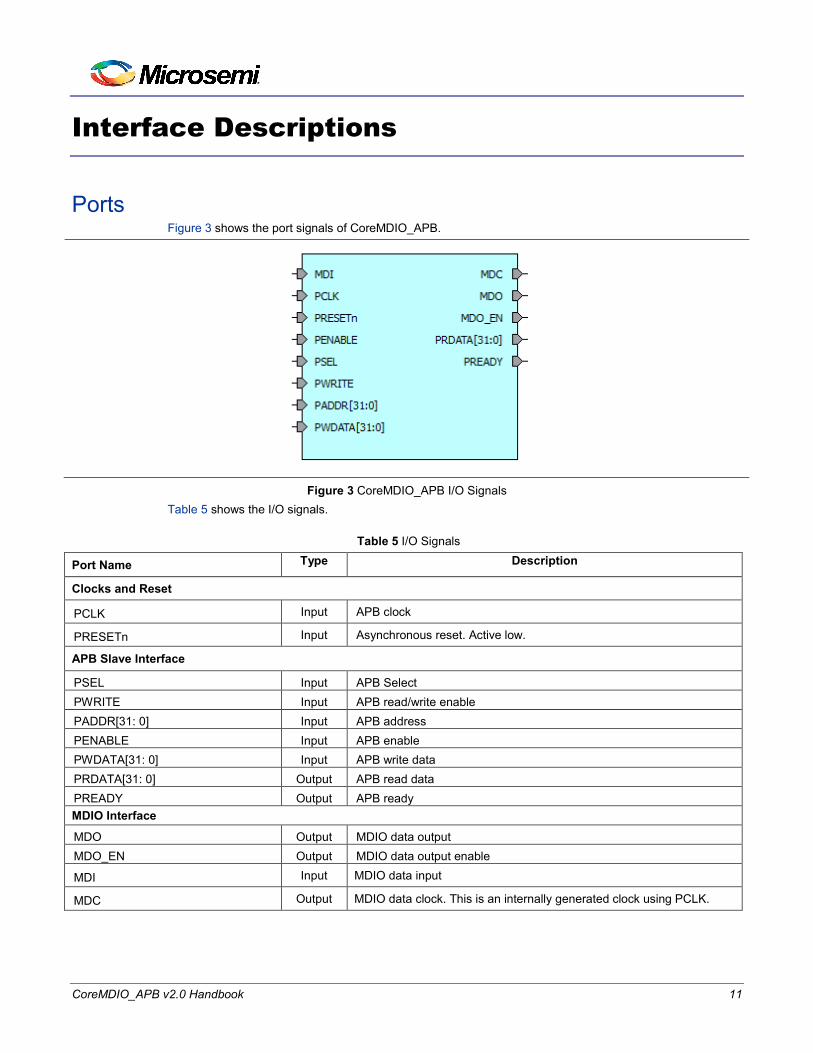
Ports Figure 3 shows the port signals of CoreMDIO_APB.
Figure 3 CoreMDIO_APB I/O Signals Table 5 shows the I/O signals.
Table 5 I/O Signals
Port Name Type Description
Clocks and Reset
PCLK Input APB clock
PRESETn Input Asynchronous reset. Active low.
APB Slave Interface
PSEL Input APB Select PWRITE Input APB read/write enable PADDR[31: 0] Input APB address PENABLE Input APB enable PWDATA[31: 0] Input APB write data PRDATA[31: 0] Output APB read data PREADY Output APB ready MDIO Interface MDO Output MDIO data output MDO_EN Output MDIO data output enable
MDI Input MDIO data input
MDC Output MDIO data clock. This is an internally generated clock using PCLK.

Interface Descriptions
12 CoreMDIO_APB v2.0 Handbook
Configuration Parameters The CoreMDIO_APB does not have any parameter or generics.

CoreMDIO_APB v2.0 Handbook 13
Timing Diagrams
For the timing diagrams, refer to the following figures at: http://standards.ieee.org/getieee802/download/802.3-2012_section2.pdf: • Figure 22–15: Behavior of MDIO during TA field of a read transaction • Figure 22–18: MDIO sourced by STA • Figure 22–19: MDIO sourced by PHY

14 CoreMDIO_APB v2.0 Handbook
Tool Flows
Licenses The CoreMDIO_APB is available with the RTL source code.
SmartDesign The CoreMDIO_APB is available for download in the Libero IP catalog through the web repository. After it is listed in the catalog, the core can be instantiated using the SmartDesign flow. For information about using SmartDesign to configure, connect, and generate cores, refer to the Libero Online Help. An example of the instantiated view is shown in Figure 4.
Figure 4 SmartDesign CoreMDIO_APB Instance View After configuring and generating the core instance, the basic functionality can be simulated using the testbench supplied with CoreMDIO_APB. The CoreMDIO_APB can be instantiated as a component of a larger design.
Simulation Flows The user testbench for CoreMDIO_APB is included in all releases. To run simulations, select the user testbench flow within SmartDesign and click Generate Design under the SmartDesign menu. The user testbench is selected through the Core Testbench Configuration GUI. When SmartDesign generates the Libero project, it will install the user testbench files. To run the user testbench, set the design root to the CoreMDIO_APB instantiation in the Libero Design Hierarchy pane and click the Simulation icon in the Libero Design Flow window. This will invoke ModelSim® and automatically run the simulation. After generating CoreMDIO_APB, the presynthesis testbench hardware description language (HDL) files are installed in Libero.
Synthesis in Libero To run synthesis on CoreMDIO_APB, set the design root to the IP component instance and run the synthesis tool from the Libero design flow pane.
Place-and-Route in Libero After the design is synthesized, run the compilation and then place-and-route the tools. The CoreMDIO_APB does not require any additional place-and-route settings.

CoreMDIO_APB v2.0 Handbook 15
Testbench Operation and Modification
A unified testbench known as user testbench is used to verify and test the CoreMDIO_APB.
User Testbench Basic unit-level verification environment is created as part of the CPZ delivery. Figure 5 shows the block diagram of the user testbench. The user testbench instantiates the CoreMDIO_APB and the behavioral code that generates APB transactions required to generate an MDIO transaction.
APB Behavioral Model CoreMDIO_APB MDIO Behavioral
Model
Figure 5 CoreMDIO_APB User Testbench The user testbench is included with the CoreMDIO_APB releases that verify the operations of MDIO.
Test Case The following are the MDIO write and read test sequences: • Configure the CoreMDIO_APB registers for an MDIO write transaction.
o Write to REG ADDR register with MDIO register address o Write to PHY ADDR register with MDIO PHY address o Write to DATA IN register with MDIO write data o Write to CONTROL register with initiate write bit asserted. o Wait for Busy status to be zero in Read status register.
• Configure the CoreMDIO_APB registers for an MDIO read transaction. o Write to REG ADDR register with MDIO register address o Write to PHY ADDR register with MDIO PHY address o Write to CONTROL register with initiate read bit asserted. o Poll for Busy status in Read status register. o Read to DATA OUT register for MDIO read data
• Compare read data with write data.

16 CoreMDIO_APB v2.0 Handbook
System Integration
Figure 6 shows an example design with the CoreMDIO_APB features and the Webserver implementation on the SmartFusion2 Security Evaluation Kit. This example design requires the following: • SmartFusion2 Ethernet MAC connected to CoreMDIO_APB for management interface. • SmartFusion2 Ethernet MAC connected to a serial gigabit media independent interface (SGMII) PHY
through CORESGMII and COREMACFILTER. • Integration of SmartFusion2 MAC driver with the lwIP TCP/IP stack and the FreeRTOS operating
system. The microcontroller subsystem (MSS) of the SmartFusion2 device has an instance of the MAC peripheral that can be configured between the host PC and the Ethernet network at the 10/100/1000 Mbps data transfer rates. For more information on the MAC interface for SmartFusion2 devices, refer to the SmartFusion2 Microcontroller Subsystem User Guide.
Figure 6 Example Design The following are some of the clock set and reset information: • POWER_ON_RESET_N from SYSRESET_0 is the reset used for CoreMDIO_APB_0. • 50 MHz PCLK is generated from FCCC_0. • The COREMDIO_APB_0 generates the 2.5 MHz MDC clock from PCLK.
System Integration
CoreMDIO_APB v2.0 Handbook 17
• The CORESGMII_0 has TXCLK, RXCLK, GTXCLK, PMA_RX_CLK0, PMA_RX_CLK1 and MDC clocks.
• 125 MHz GTXCLK clock is generated from FCCC_2. TXCLK and RXCLK are 2.5, 25, and 125 MHz are generated from FCCC_3 depending on 10/100/1000 Mbps respectively. 62.5 MHz PMA_RX_CLK0 and PMA_RX_CLK1 are generated from FCCC_1. PMA_RX_CLK1 is 180 degree phase shift with PMA_RX_CLK0.
Run the Libero flow with the timing driven and high effort place and route options enabled. The example design clock constraints are included in the core package, generated under the Libero SmartDesign path: /component/Actel/DirectCore/CoreMDIO_APB/ <Core version number>/constraints/
18 CoreMDIO_APB v2.0 Handbook
Ordering Information
Ordering Codes The CoreMDIO_APB can be ordered through the local sales representatives. It must be ordered using the following number scheme: CoreMDIO_APB-XX, where XX is shown in Table 6.
Table 6 Ordering Codes XX Description RM Available as RTL source code.

CoreMDIO_APB v2.0 Handbook 19
List of Changes
The following table shows important changes made in this document for each revision. Date and Revision Change Page Revision 1 (August 2015)
Initial release. NA

20 CoreMDIO_APB v2.0 Handbook
Product Support
Microsemi SoC Products Group backs its products with various support services, including Customer Service, Customer Technical Support Center, a website, electronic mail, and worldwide sales offices. This appendix contains information about contacting Microsemi SoC Products Group and using these support services.
Customer Service Contact Customer Service for non-technical product support, such as product pricing, product upgrades, update information, order status, and authorization.
From North America, call 800.262.1060 From the rest of the world, call 650.318.4460 Fax, from anywhere in the world 408.643.6913
Customer Technical Support Center Microsemi SoC Products Group staffs its Customer Technical Support Center with highly skilled engineers who can help answer your hardware, software, and design questions about Microsemi SoC Products. The Customer Technical Support Center spends a great deal of time creating application notes, answers to common design cycle questions, documentation of known issues and various FAQs. So, before you contact us, please visit our online resources. It is very likely we have already answered your questions.
Technical Support For Microsemi SoC Products Support, visit http://www.microsemi.com/products/fpga-soc/design-support/fpga-soc-support
Website You can browse a variety of technical and non-technical information on the Microsemi SoC Products Group home page, at http://www.microsemi.com/soc/.
Contacting the Customer Technical Support Center Highly skilled engineers staff the Technical Support Center. The Technical Support Center can be contacted by email or through the Microsemi SoC Products Group website.
Email You can communicate your technical questions to our email address and receive answers back by email, fax, or phone. Also, if you have design problems, you can email your design files to receive assistance. We constantly monitor the email account throughout the day. When sending your request to us, please be sure to include your full name, company name, and your contact information for efficient processing of your request. The technical support email address is [email protected].

Product Support
CoreMDIO_APB v2.0 Handbook 21
My Cases Microsemi SoC Products Group customers may submit and track technical cases online by going to My Cases.
Outside the U.S. Customers needing assistance outside the US time zones can either contact technical support via email ([email protected]) or contact a local sales office. Sales office listings can be found at www.microsemi.com/soc/company/contact/default.aspx.
ITAR Technical Support For technical support on RH and RT FPGAs that are regulated by International Traffic in Arms Regulations (ITAR), contact us via [email protected]. Alternatively, within My Cases, select Yes in the ITAR drop-down list. For a complete list of ITAR-regulated Microsemi FPGAs, visit the ITAR web page.
Microsemi Corporation (MSCC) offers a comprehensive portfolio of semiconductor and system solutions for communications, defense & security, aerospace and industrial markets. Products include high-performance and radiation-hardened analog mixed-signal integrated circuits, FPGAs, SoCs and ASICs; power management products; timing and synchronization devices and precise time solutions, setting the world's standard for time; voice processing devices; RF solutions; discrete components; security technologies and scalable anti-tamper products; Ethernet solutions; Power-over-Ethernet ICs and midspans; as well as custom design capabilities and services. Microsemi is headquartered in Aliso Viejo, Calif., and has approximately 3,600 employees globally. Learn more at www.microsemi.com. Microsemi Corporate Headquarters
One Enterprise, Aliso Viejo, CA 92656 USA Within the USA: +1 (800) 713-4113 Outside the USA: +1 (949) 380-6100 Sales: +1 (949) 380-6136 Fax: +1 (949) 215-4996 E-mail: [email protected]
© 2015 Microsemi Corporation. All rights reserved. Microsemi and the Microsemi logo are trademarks of Microsemi Corporation. All other trademarks and service marks are the property of their respective owners.
50200647-1/08.15
Microsemi makes no warranty, representation, or guarantee regarding the information contained herein or the suitability of its products and services for any particular purpose, nor does Microsemi assume any liability whatsoever arising out of the application or use of any product or circuit. The products sold hereunder and any other products sold by Microsemi have been subject to limited testing and should not be used in conjunction with mission-critical equipment or applications. Any performance specifications are believed to be reliable but are not verified, and Buyer must conduct and complete all performance and other testing of the products, alone and together with, or installed in, any end-products. Buyer shall not rely on any data and performance specifications or parameters provided by Microsemi. It is the Buyer’s responsibility to independently determine suitability of any products and to test and verify the same. The information provided by Microsemi hereunder is provided “as is, where is” and with all faults, and the entire risk associated with such information is entirely with the Buyer. Microsemi does not grant, explicitly or implicitly, to any party any patent rights, licenses, or any other IP rights, whether with regard to such information itself or anything described by such information. Information provided in this document is proprietary to Microsemi, and Microsemi reserves the right to make any changes to the information in this document or to any products and services at any time without notice.