course code course name l-t-p-c year of …ce-kgr.org/wp-content/uploads/2017/11/electronics... ·...
TRANSCRIPT

COURSE CODE COURSE NAME L-T-P-C YEAR OF
INTRODUCTION
EC201 NETWORK THEORY 3-1-0-4 2016
Prerequisite: Nil
Course objectives:
To make the students capable of analyzing any linear time invariant electrical network.
To study time domain, phasor and Laplace transform methods of linear circuit analysis.
To study the transient response of networks subject to test signals.
To develop understanding of the concept of resonance, coupled circuits and two port
networks.
Syllabus:
Circuit variables and Circuit elements, Kirchhoff’s laws, Network topology, Mesh and node
analysis of network, Laplace transform, Inverse Laplace transform, Solution of differential
equations by using Laplace transforms, Transient analysis of RL, RC, and RLC networks, Network
functions for the single port and two ports, Parameters of two-port network, Resonance, Coupled
circuits
Expected outcome:
At the end of the course students will be able to analyze the linear time invariant electrical circuits.
Text Books
1. Ravish R., Network Analysis and Synthesis, 2/e, McGraw-Hill, 2015.
2. Valkenburg V., Network Analysis, 3/e, PHI, 2011.
References:
1. Sudhakar A,S. P. Shyammohan, Circuits and Networks- Analysis and Synthesis, 5/e, McGraw-
Hill, 2015.
2. Choudhary R., Networks and Systems, 2/e, New Age International, 2013.
3. Franklin F. Kuo, Network Analysis and Synthesis, 2/e, Wiley India, 2012.
4. Pandey S. K., Fundamentals of Network Analysis and Synthesis, 1/e, S. Chand, 2012.
5. Edminister, Electric Circuits – Schaum’s Outline Series, McGraw-Hill,2009.
Course Plan
Module Course content (48 hrs) Hours Sem.
Exam
Marks
I
Introduction to circuit variables and circuit elements, Review of
Kirchhoff’s Laws, Independent and dependent Sources, Source
transformations
3
15
Network topology, Network graphs, Trees, Incidence matrix,
Tie-set matrix and Cut-set matrix
2
Solution methods applied to dc and phasor circuits: Mesh and node
analysis of network containing independent and dependent sources
3
II Network theorems applied to dc and phasor circuits: Thevenin’s
theorem, Norton’s theorem, Superposition theorem, Reciprocity
theorem, Millman’s theorem, Maximum power transfer theorem
6 15

Laplace transform, properties
Laplace Transforms and inverse Laplace transform of common
functions, Important theorems: Time shifting theorem, Frequency
shifting theorem, Time differentiation theorem, Time integration
theorem, s domain differentiation theorem, s domain integration
theorem, Initial value theorem, Final value theorem
4
FIRST INTERNAL EXAM
III Partial Fraction expansions for inverse Laplace transforms,
Solution of differential equations using Laplace transforms
3
15
Transformation of basic signals and circuits into s-domain 2
Transient analysis of RL, RC, and RLC networks with impulse, step,
pulse, exponential and sinusoidal inputs
3
Analysis of networks with transformed impedance and dependent
sources.
3
IV Network functions for the single port and two ports, properties of
driving point and transfer functions,
Poles and Zeros of network functions, Significance of Poles and
Zeros
3 15
Time domain response from pole zero plot, Impulse Response 1
Network functions in the sinusoidal steady state, Magnitude and
Phase response
3
SECOND INTERNAL EXAM
V Parameters of two port network: impedance, admittance,
transmission and hybrid parameters, Interrelationship among
parameter sets
5 20
Series and parallel connections of two port networks 2
Reciprocal and Symmetrical two port network 2
Characteristic impedance, Image impedance and propagation
constant (derivation not required)
2
VI Resonance: Series resonance, bandwidth, Q factor and Selectivity,
Parallel resonance
3 20
Coupled circuits: single tuned and double tuned circuits, dot
convention, coefficient of coupling, Analysis of coupled circuits
4
END SEMESTER EXAM
Question Paper Pattern
The question paper consists of three parts. Part A covers modules I and II, Part B covers modules III and
IV and Part C covers modules V and VI. Each part has three questions. Each question can have a
maximum of four subparts. Among the three questions one will be a compulsory question covering both
the modules and the remaining two questions will be as one question from each module, of which one is
to be answered. Mark pattern is according to the syllabus with maximum 30% for theory and 70% for
logical/numerical problems, derivation and proof.

Course code Course Name L-T-P - Credits Year of
Introduction
EC202 SIGNALS & SYSTEMS 3-1-0 -4 2016
Prerequisite: Nil
Course Objectives
1. To train students for an intermediate level of fluency with signals and systems in both
continuous time and discrete time, in preparation for more advanced subjects in digital signal
processing, image processing, communication theory and control systems.
2. To study continuous and discrete-time signals and systems, their properties and
representations and methods those are necessary for the analysis of continuous and discrete-
time signals and systems.
3. To familiarize with techniques suitable for analyzing and synthesizing both continuous-time
and discrete time systems.
4. To gain knowledge of time-domain representation and analysis concepts as they relate to
differential equations, difference equations, impulse response and convolution, etc.
5. To study frequency-domain representation and analysis concepts using Fourier analysis tools,
Laplace Transform and Z-transform.
To study concepts of the sampling process, reconstruction of signals and interpolation.
Syllabus
Elementary signals, Continuous time and Discrete time signals and systems, Signal operations,
Differential equation representation, Difference equation representation, Continuous time LTI
Systems, Discrete time LTI Systems, Correlation between signals, Orthogonality of signals,
Frequency domain representation, Continuous time Fourier series, Continuous time Fourier
transform, Laplace transform, Inverse Laplace transform, Unilateral Laplace transform, Transfer
function, Frequency response, Sampling, Aliasing, Z transform, Inverse Z transform, Unilateral Z
transform, Frequency domain representation of discrete time signals, Discrete time Fourier series
and discrete time Fourier transform (DTFT), Analysis of discrete time LTI systems using the
above transforms
Expected outcome . The student will be able to:
i. Define, represent, classify and characterize basic properties of continuous and discrete
time signals and systems.
ii. Represent the CT signals in Fourier series and interpret the properties of Fourier
transform and Laplace transform
iii. Outline the relation between convolutions, correlation and to describe the orthoganality of
signals.
iv. Illustrate the concept of transfer function and determine the magnitude and phase response
of LTI systems.
v. Explain sampling theorem and techniques for sampling and reconstruction.
vi. Determine z transforms, inverse z transforms and analyze LTI systems using z transform.
Text Book:
1. Alan V. Oppenheim and Alan Willsky, Signals and Systems, PHI, 2/e, 2009
2. Simon Haykin, Signals & Systems, John Wiley, 2/e, 2003
References: 1. Anand Kumar, Signals and Systems, PHI, 3/e, 2013.
2. B P. Lathi, Priciples of Signal Processing & Linear systems, Oxford University Press.
3. Gurung, Signals and System, PHI.
4. Mahmood Nahvi, Signals and System, Mc Graw Hill (India), 2015.
5. P Ramakrishna Rao, Shankar Prakriya, Signals and System, MC Graw Hill Edn 2013.
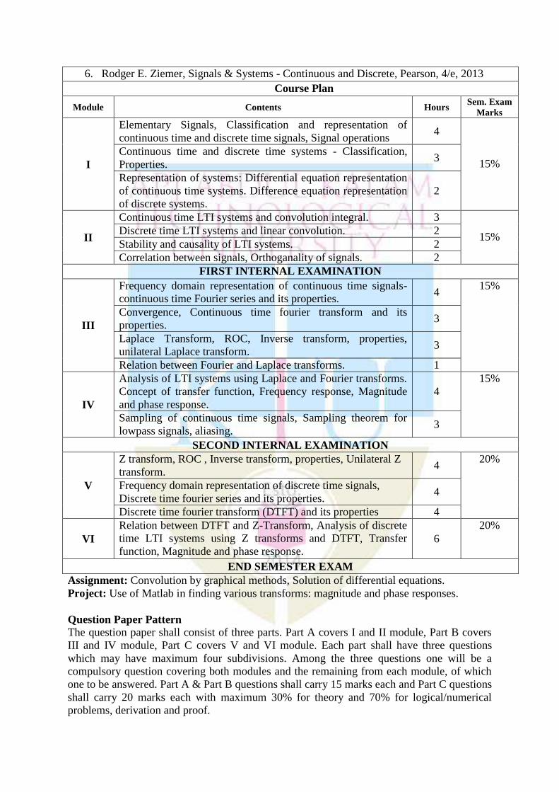
6. Rodger E. Ziemer, Signals & Systems - Continuous and Discrete, Pearson, 4/e, 2013
Course Plan
Module Contents Hours Sem. Exam
Marks
I
Elementary Signals, Classification and representation of
continuous time and discrete time signals, Signal operations 4
15% Continuous time and discrete time systems - Classification,
Properties. 3
Representation of systems: Differential equation representation
of continuous time systems. Difference equation representation
of discrete systems.
2
II
Continuous time LTI systems and convolution integral. 3
15% Discrete time LTI systems and linear convolution. 2
Stability and causality of LTI systems. 2
Correlation between signals, Orthoganality of signals. 2
FIRST INTERNAL EXAMINATION
III
Frequency domain representation of continuous time signals-
continuous time Fourier series and its properties. 4
15%
Convergence, Continuous time fourier transform and its
properties. 3
Laplace Transform, ROC, Inverse transform, properties,
unilateral Laplace transform. 3
Relation between Fourier and Laplace transforms. 1
IV
Analysis of LTI systems using Laplace and Fourier transforms.
Concept of transfer function, Frequency response, Magnitude
and phase response.
4
15%
Sampling of continuous time signals, Sampling theorem for
lowpass signals, aliasing. 3
SECOND INTERNAL EXAMINATION
V
Z transform, ROC , Inverse transform, properties, Unilateral Z
transform. 4
20%
Frequency domain representation of discrete time signals,
Discrete time fourier series and its properties. 4
Discrete time fourier transform (DTFT) and its properties 4
VI
Relation between DTFT and Z-Transform, Analysis of discrete
time LTI systems using Z transforms and DTFT, Transfer
function, Magnitude and phase response. 6
20%
END SEMESTER EXAM
Assignment: Convolution by graphical methods, Solution of differential equations.
Project: Use of Matlab in finding various transforms: magnitude and phase responses.
Question Paper Pattern
The question paper shall consist of three parts. Part A covers I and II module, Part B covers
III and IV module, Part C covers V and VI module. Each part shall have three questions
which may have maximum four subdivisions. Among the three questions one will be a
compulsory question covering both modules and the remaining from each module, of which
one to be answered. Part A & Part B questions shall carry 15 marks each and Part C questions
shall carry 20 marks each with maximum 30% for theory and 70% for logical/numerical
problems, derivation and proof.

COURSE
CODE
COURSE NAME L-T-P-C YEAR OF
INTRODUCTION
EC203 SOLID STATE DEVICES 3-1-0-4 2016
Prerequisite: Nil
Course objectives:
To provide an insight into the basic semiconductor concepts
To provide a sound understanding of current semiconductor devices and technology to
appreciate its applications to electronics circuits and systems
Syllabus: Elemental and compound semiconductors, Fermi-Dirac distribution, Equilibrium and
steady state conditions: Equilibrium concentration of electrons and holes, Temperature
dependence of carrier concentration, Carrier transport in semiconductors, High field effects,
Hall effect, Excess carriers in semiconductors , PN junctions ,contact potential, electrical field,
potential and charge density at the junction, energy band diagram, minority carrier distribution,
ideal diode equation, electron and hole component of current in forward biased pn junction,
piecewise linear model of a diode , effect of temperature on VI characteristics, Diode
capacitances, electrical breakdown in pn junctions, Tunnel Diode, Metal semiconductor
contacts, bipolar junction transistor, metal insulator semiconductor devices, MOSFET, FinFET
Expected outcome: The students should have a good knowledge in semiconductor theory and electronic devices.
Text Books:
1. Ben G. Streetman and Sanjay Kumar Banerjee, Solid State Electronic Devices, Pearson, 6/e,
2010
2. Achuthan, K N Bhat, Fundamentals of Semiconductor Devices, 1e, McGraw Hill,2015
References:
1. Tyagi M.S., Introduction to Semiconductor Materials and Devices, Wiley India, 5/e, 2008
2. Sze S.M., Physics of Semiconductor Devices, John Wiley, 3/e, 2005
3. Neamen, Semiconductor Physics and Devices, McGraw Hill, 4/e, 2012
4. Pierret, Semiconductor Devices Fundamentals, Pearson, 2006
5. Rita John, Solid State Devices, McGraw-Hill, 2014
6. Bhattacharya .Sharma, Solid State Electronic Devices, Oxford University Press, 2012
7. Dasgupta and Dasgupta , Semiconductor Devices : Modelling and Technology (PHI)
Course Plan
Module Course content (48hrs) Hours Sem.
Exam
Marks
I Elemental and compound semiconductors, Fermi-Dirac
distribution, Equilibrium and steady state conditions, Equilibrium
concentration of electrons and holes, Temperature dependence of
carrier concentration
4 15
Carrier transport in semiconductors, drift, conductivity and
mobility, variation of mobility with temperature and doping,
High Field Effects, Hall effect
5
II Excess carriers in semiconductors: Generation and recombination
mechanisms of excess carriers, quasi Fermi levels, diffusion,
Einstein relations, Continuity equations, Diffusion length,
Gradient of quasi Fermi level
9 15
FIRST INTERNAL EXAM

III PN junctions : Contact potential, Electrical Field, Potential and
Charge density at the junction, Energy band diagram, Minority
carrier distribution, Ideal diode equation, Electron and hole
component of current in forward biased p-n junction, piecewise
linear model of a diode effect of temperature on V-I characteristics
9 15
IV Diode capacitances, switching transients, Electrical Breakdown in
PN junctions, Zener and avalanche break down (abrupt PN
junctions only), Tunnel Diode basics only, Metal Semiconductor
contacts, Ohmic and Rectifying Contacts, current voltage
characteristics
9 15
SECOND INTERNAL EXAM
V Bipolar junction transistor , current components, Minority carrier
distributions, basic parameters, Evaluation of terminal currents
(based on physical dimensions),Transistor action, Base width
modulation
9 20
VI Metal Insulator semiconductor devices: The ideal MOS capacitor,
band diagrams at equilibrium, accumulation, depletion and
inversion, surface potential, CV characteristics, effects of real
surfaces, work function difference, interface charge, threshold
voltage
MOSFET: Output characteristics, transfer characteristics, sub
threshold characteristics, MOSFET scaling (basic concepts)
9 20
FinFET-structure and operation 1
END SEMESTER EXAM
Question Paper Pattern
The question paper consists of three parts. Part A covers modules I and II, Part B covers modules III and
IV and Part C covers modules V and VI. Each part has three questions. Each question can have a
maximum of four subparts. Among the three questions one will be a compulsory question covering both
the modules and the remaining two questions will be as one question from each module, of which one is
to be answered. Mark pattern is according to the syllabus with maximum 70 % for theory, derivation,
proof and 30% for logical/numerical problems.

Course code Course Name L-T-P -
Credits
Year of
Introduction
EC204 ANALOG INTEGRATED CIRCUITS 4-0-0-4 2016
Prerequisite: Nil
Course Objectives
To equip the students with a sound understanding of fundamental concepts of operational
amplifiers
To understand the wide range of applications of operational amplifiers
To introduce special function integrated circuits
To introduce the basic concepts and types of data converters
Syllabus
Differential amplifier configurations, Operational amplifiers, Block diagram, Ideal op-amp
parameters, Effect of finite open loop gain, bandwidth and slew rate on circuit performance, op-
amp applications-linear and nonlinear, Active filters, Specialized ICs and their applications,
Monolithic Voltage Regulators - types and its applications, Data converters - specifications and
types.
Expected outcome .
The students will
i. have a thorough understanding of operational amplifiers
ii. be able to design circuits using operational amplifiers for various applications
Text Book:
1. Franco S., Design with Operational Amplifiers and Analog Integrated Circuits, 3/e, Tata
McGraw Hill, 2008
2. Salivahanan S. ,V. S. K. Bhaaskaran, Linear Integrated Circuits, Tata McGraw Hill, 2008
References: 1. Botkar K. R., Integrated Circuits, 10/e, Khanna Publishers, 2010
2. C.G. Clayton, Operational Amplifiers, Butterworth & Company Publ. Ltd. Elsevier, 1971
3. David A. Bell, Operational Amplifiers & Linear ICs, Oxford University Press, 2nd
edition,
2010
4. Gayakwad R. A., Op-Amps and Linear Integrated Circuits, Prentice Hall, 4/e, 2010
5. R.F. Coughlin & Fredrick Driscoll, Operational Amplifiers & Linear Integrated Circuits,
6th
Edition, PHI,2001
6. Roy D. C. and S. B. Jain, Linear Integrated Circuits, New Age International, 3/e, 2010
7. Sedra A. S. and K. C. Smith, Microelectronic Circuits, 6/e, Oxford University Press, 2013
Course Plan
Module Contents Hours Sem. Exam Marks
I
Differential amplifiers: Differential amplifier configurations using
BJT, Large and small signal operations, Input resistance, Voltage
gain, CMRR, Non-ideal characteristics of differential amplifier.
Frequency response of differential amplifiers, Current sources,
Active load, Concept of current mirror circuits, Wilson current
mirror circuits (Analysis using hybrid ‘pi’ model only).
6
15%
Operational amplifiers: Introduction, Block diagram, Ideal op-amp
parameters, Equivalent circuit, Voltage transfer curve, Open loop
op-amp configurations, Effect of finite open loop gain, Bandwidth
and slew rate on circuit performance
5
II Op-amp with negative feedback: Introduction, Feedback 3 15%

configurations, Voltage series feedback, Voltage shunt feedback,
Properties of practical op-amp.
Op-amp applications: Inverting and non inverting amplifier, DC
and AC amplifiers, Summing, Scaling and averaging amplifiers,
Instrumentation amplifier.
4
FIRST INTERNAL EXAMINATION
III
Op-amp applications: Voltage to current converter, Current to
voltage converter, Integrator, Differentiator, Precision rectifiers,
Log and antilog amplifier, Phase shift and Wien bridge oscillators
7 15%
IV
Astable and monostable multivibrators, Triangular and saw tooth
wave generators, Comparators, Zero crossing detector, Schmitt
trigger
5
15% Active filters: Advantages, First and second order low pass, High
pass, Band pass and band reject filters, Design of filters using
Butterworth approximations
5
SECOND INTERNAL EXAMINATION
V
Specialized ICs and its applications:
Timer IC 555 : Astable and monostable operations, applications.
Analog Multipliers: Introduction, Gilbert multiplier cell.
Voltage Controlled Oscillator IC AD633 and their applications.
3
20%
Phase Locked Loop – Operation, Closed loop analysis, Lock and
capture range, Basic building blocks, PLL IC 565, Applications of
PLL for AM & FM detection and Frequency multiplication,
Frequency division, Frequency synthesizing.
4
Monolithic Voltage Regulators - Fixed voltage regulators, 78XX
and 79XX series, Adjustable voltage regulators, IC 723 – Low
voltage and high voltage configurations, Current boosting, Current
limiting, Short circuit and Fold-back protection.
4
VI
Data Converters: D/A converter, Specifications, Weighted resistor
type, R-2R Ladder type. 3
20%
A/D Converters: Specifications, Classification, Flash type,
Counter ramp type, Successive approximation type, Single slope
type, Dual slope type, Sample-and-hold circuits.
5
END SEMESTER EXAM
Assignment
1. Explain the importance of frequency compensated networks in opamps and the
commonly used compensation techniques.
2. Write short notes on commercially available integrated circuits (Opamp, ADC, DAC,
VCO, Analog multiplier, PLL ) with pin outs and their important features
Question Paper Pattern
The question paper shall consist of three parts. Part A covers I and II module, Part B covers
III and IV module, Part C covers V and VI module. Each part has three questions, which may
have maximum four subdivisions. Among the three questions, one will be a compulsory
question covering both modules and the remaining from each module, of which, one to be
answered. Part A & Part B questions shall carry 15 marks each and Part C questions shall
carry 20 marks each with maximum 60% for theory and 40% for logical/numerical problems,
derivation and proof.

COURSE
CODE
COURSE NAME L-T-P-
C
YEAR OF
INTRODUCTION
EC205 ELECTRONIC CIRCUITS 3-1-0-4 2016
Prerequisite: Nil
Course objectives:
To develop the skill of analysis and design of various analog circuits using discrete
electronic devices as per the specifications.
Syllabus:
High pass and low pass RC circuits, Differentiator, Integrator, Analysis of BJT biasing circuits,
small signal analysis of transistor configurations using small signal hybrid π model, low
frequency and high frequency analysis of BJT amplifiers, Cascade amplifiers, Wide band
amplifiers, Feedback amplifiers, Oscillators, Tuned amplifiers, Power amplifiers, Sweep circuits
and multivibrators, transistor voltage regulator, DC analysis of MOSFET circuits, small signal
equivalent circuit, Small signal analysis of MOSFET amplifier circuits, Analysis of multistage
MOSFET amplifiers
Expected outcome:
At the end of the course, students will be able to analyse and design the different
electronic circuits using discrete electronic components.
Text Books:
Sedra A. S. and K. C. Smith, Microelectronic Circuits, 6/e, Oxford University Press, 2013
Millman J. and C. Halkias, Integrated Electronics, 2/e, McGraw-Hill, 2010
References:
1. Neamen D., Electronic Circuits - Analysis and Design, 3/e, TMH, 2007
2. Rashid M. H., Microelectronic Circuits - Analysis and Design, Cengage Learning, 2/e,
2011
3. Spencer R. R. and M. S. Ghausi, Introduction to Electronic Circuit Design, Pearson, 2003
4. Razavi B., Fundamentals of Microelectronics, Wiley, 2015
Course Plan
Module Course content (48 hrs) Hours Sem.
Exam
Marks
I
RC Circuits: Response of high pass and low pass RC circuits to
sine, step, pulse and square wave inputs, Differentiator, Integrator
5
15
BJT biasing circuits: Types, Q point, Bias stability, Stability
factors, RC coupled amplifier and effect of various components,
Concept of DC and AC load lines, Fixing of operating point,
Classification of amplifiers
5
II
Small signal analysis of CE, CB and CC configurations using small
signal hybrid π model (gain, input and output impedance). Small
signal analysis of BJT amplifier circuits, Cascade amplifier
7 15
FIRST INTERNAL EXAM
III High frequency equivalent circuits of BJT, Short circuit current
gain, cutoff frequency, Miller effect, Analysis of high frequency
response of CE, CB and CC amplifiers
4
15
Wide band amplifier: Broad banding techniques, low frequency
and high frequency compensation, Cascode amplifier.
4
IV Feedback amplifiers: Effect of positive and negative feedback on
gain, frequency response and distortion, Feedback topologies and
3 15

its effect on input and output impedance, Feedback amplifier
circuits in each feedback topologies (no analysis required)
Oscillators & Tuned Amplifiers: Classification of oscillators,
Barkhausen criterion, Analysis of RC phase shift and Wien bridge
oscillators, Working of Hartley, Colpitts and Crystal oscillators;
Tuned amplifiers, synchronous and stagger tuning
6
SECOND INTERNAL EXAM
V Power amplifiers: Classification, Transformer coupled class A
power amplifier, push pull class B and class AB power amplifiers,
efficiency and distortion, Transformer-less class B and Class AB
power amplifiers, Class C power amplifier (no analysis required)
6 20
Switching Circuits: Simple sweep circuit, Bootstrap sweep circuit,
Astable, Bistable, and Monostable multivibrators, Schmitt Trigger
5
VI Transistor based voltage regulator: Design and analysis of shunt and
series voltage regulator, load and line regulation, Short circuit
protection
4 20
MOSFET amplifiers: Biasing of MOSFET amplifier, DC analysis of
single stage MOSFET amplifier, small signal equivalent circuit.
Small signal voltage and current gain, input and output impedances
of CS configuration, MOSFETCascade amplifier
5
END SEMESTER EXAM
Question Paper Pattern
The question paper consists of three parts. Part A covers modules I and II, Part B covers modules III and
IV and Part C covers modules V and VI. Each part has three questions. Each question can have a
maximum of four subparts. Among the three questions one will be a compulsory question covering both
the modules and the remaining two questions will be as one question from each module, of which one is
to be answered. Mark pattern is according to the syllabus with maximum 60 % for theory, derivation,
proof and 40% for logical/numerical problems.

Course
code
Course Name L-T-P -
Credits
Year of
Introduction
EC206 COMPUTER ORGANISATION 3-0-0-3 2016
Prerequisite: EC207 Logic Circuit Design
Course Objectives
To impart knowledge in computer architecture.
To impart knowledge in machine language programming.
To develop understanding on I/O accessing techniques and memory structures.
Syllabus
Functional units of a computer, Arithmetic circuits, Processor architecture, Instructions and
addressing modes, Execution of program, Micro architecture design process, Design of data path
and control units, I/O accessing techniques, Memory concepts, Memory interface, Cache and
Virtual memory concepts.
Expected outcome .
The students will be able to:
i. Understand the functional units of a computer
ii. Identify the different types of instructions
iii. Understand the various addressing modes
iv. Understand the I/O addressing system
v. Categorize the different types of memories
Text Book:
1. David A. Patterson and John L. Hennessey, Computer Organisation and Design, Fourth
Edition, Morgan Kaufmann
2. David Money Harris, Sarah L Harris, Digital Design and Computer Architecture,Morgan
Kaufmann – Elsevier, 2009
References: 1. Carl Hamacher : “Computer Organization ”, Fifth Edition, Mc Graw Hill
2. John P Hayes: “Computer Architecture and Organisation”, Mc Graw Hill
3. William Stallings: “Computer Organisation and Architecture”, Pearson Education
4. Andrew S Tanenbaum: “Structured Computer Organisation”, Pearson Education
5. Craig Zacker: “PC Hardware : The Complete Reference”, TMH
Course Plan
Module Contents Hours Sem. Exam Marks
I
Functional units of a computer
Arithmetic Circuits: Adder-carry propagate adder, Ripple carry
adder, Basics of carry look ahead and prefix adder, Subtractor,
Comparator, ALU
4
15%
Shifters and rotators, Multiplication, Division 3
Number System: Review of Fixed point & Floating point number
system 1
II
Architecture : Assembly Language, Instructions, Operands,
Registers, Register set, Memory, Constants 2
15% Machine Language: R-Type, I-Type, J-Type Instructions,
Interpreting machine language code 3
FIRST INTERNAL EXAMINATION
III MIPS Addressing modes – Register only, Immediate, Base, PC-
relative, Pseudo - direct 3 15%

MIPS memory map, Steps for executing a program - Compilation,
Assembling, Linking, Loading 3
Pseudoinstuctions, Exceptions, Signed and Unsigned instructions,
Floating point instructions 3
IV
MIPS Microarchitectures – State elements of MIPS processor 1
15%
Design process and performance analysis of Single cycle
processor, Single cycle data path, Single cycle control for R – type
arithmetic/logical instructions.
3
Design process and performance analysis of multi cycle processor,
Multi cycle data path, Multi cycle control for R – type
arithmetic/logical instructions.
3
SECOND INTERNAL EXAMINATION
V
I/O system – Accessing I/O devices, Modes of data transfer,
Programmed I/O, Interrupt driven I/O, Direct Memory Access,
Standard I/O interfaces – Serial port, Parallel port, PCI, SCSI, and
USB.
3
20%
Memory system – Hierarchy, Characteristics and Performance
analysis, Semiconductor memories (RAM, ROM, EPROM),
Memory Cells – SRAM and DRAM, internal organization of a
memory chip, Organization of a memory unit.
4
VI
Cache Memory – Concept/principle of cache memory, Cache size,
mapping methods – direct, associated, set associated, Replacement
algorithms, Write policy- Write through, Write back.
3
20%
Virtual Memory – Memory management, Segmentation, Paging,
Address translation, Page table, Translation look aside buffer. 3
END SEMESTER EXAM
Question Paper Pattern
The question paper shall consist of three parts. Part A covers I and II module, Part B covers
III and IV module, Part C covers V and VI module. Each part has three questions, which may
have maximum four subdivisions. Among the three questions, one will be a compulsory
question covering both modules and the remaining from each module, of which one to be
answered. Part A & Part B questions shall carry 15 marks each and Part C questions shall
carry 20 marks each with maximum 80 % for theory and 20% for logical/numerical
problems, derivation and proof.

COURSE
CODE
COURSE NAME L-T-P-C YEAR OF
INTRODUCTION
EC207 LOGIC CIRCUIT DESIGN 3-0-0-3 2016
Prerequisite:Nil
Course objectives:
To work with a positional number systems and numeric representations
To introduce basic postulates of Boolean algebra and show the correlation between Boolean
expression
To outline the formal procedures for the analysis and design of combinational circuits and
sequential circuits
To study the fundamentals of HDL
To design and implement combinational circuits using basic programmable blocks
To design and implement synchronous sequential circuits
Syllabus:
Positional Number Systems, Boolean algebra, Combinational Logic, HDL concepts ,Digital ICs,
Programmable Logic Devices, Sequential Logic, Sequential Circuits
Expected outcome:
The student should able to:
1. Compare various positional number systems and binary codes
2. Apply Boolean algebra in logic circuit design
3. Design combinational and sequential circuits
4. Design and implement digital systems using basic programmable blocks
5. Formulate various digital systems using HDL
Text Books:
1. Donald D Givone, Digital Principles and Design, Tata McGraw Hill, 2003
2. John F Wakerly, Digital Design Principles and Practices, Pearson Prentice Hall, 2007
References: 1.Ronald J Tocci, Digital Systems, Pearson Education, 11
th edition,2010
2.Thomas L Floyd, Digital Fundamentals, Pearson Education, 8th
edition 2009
3.Moris Mano, Digital Design, Prentice Hall of India, 3rd
edition, 2002
4.John M Yarbrough, Digital Logic Applications and Design, Cenage learning, 2009
5.David Money Harris, Sarah L Harris, Digital Design and Computer Architecture, Morgan
Kaufmann – Elsevier, 2009
Course Plan
Modul
e
Course content (42 hrs) Hours Sem.
Exam
Marks
I Number systems- decimal, binary, octal, hexa decimal, base conversion 2 15
1’s and 2’s complement, signed number representation
Binary arithmetic, binary subtraction using 2’s complement
2
Binary codes (grey, BCD and Excess-3), Error detection and correcting
codes : Parity(odd, even), Hamming code (7,4), Alphanumeric codes :
ASCII
2
II Logic expressions, Boolean laws, Duality, De Morgan's law, Logic
functions and gates
2 15
Canonical forms: SOP, POS, Realisation of logic expressions using K- 2

map (2,3,4 variables)
Design of combinational circuits – adder, subtractor, 4 bit
adder/subtractor, BCD adder, MUX, DEMUX, Decoder,BCD to 7
segment decoder, Encoder, Priority encoder, Comparator (2/3 bits)
4
FIRST INTERNAL EXAM
III Introduction to HDL : Logic descriptions using HDL, basics of
modeling (only for assignments) 2 0
Logic families and its characteristics: Logic levels, propagation delay,
fan in, fan out, noise immunity , power dissipation, TTL subfamilies
1 15
NAND in TTL (totem pole, open collector and tri-state),
CMOS:NAND, NOR, and NOT in CMOS, Comparison of logic
families (TTL,ECL,CMOS) in terms of fan-in, fan-out, supply voltage,
propagation delay, logic voltage and current levels, power dissipation
and noise margin
2
Programmable Logic devices - ROM, PLA, PAL, implementation of
simple circuits using PLA
2
IV Sequential circuits - latch, flip flop ( SR, JK, T, D), master slave JK FF,
conversion of FFs, excitation table and characteristic equations
3 15
Asynchronous and synchronous counter design, mod N counters,
random sequence generator
5
SECOND INTERNAL EXAM
V Shift Registers - SIPO, SISO, PISO, PIPO, Shift registers with parallel
LOAD/SHIFT
Shift register counter - Ring Counter and Johnson Counter
3 20
Mealy and Moore models, state machine ,notations, state diagram, state
table, transition table, excitation table, state equations
3
VI Construction of state diagram – up down counter, sequence detector 3 20
Synchronous sequential circuit design - State equivalence 2
State reduction – equivalence classes, implication chart 2
END SEMESTER EXAM
Assignments:
1. Simple combinational circuit design using MUX,DEMUX, PLA & PAL
2. HDL simulation of circuits like simple ALU, up-down counter, linear feedback shift register,
sequence generator
Question Paper Pattern
The question paper consists of three parts. Part A covers modules I and II, Part B covers modules III and
IV and Part C covers modules V and VI. Each part has three questions. Each question have a maximum
of four subparts. Among the three questions one will be a compulsory question covering both the
modules and the remaining two questions will be as one question from each module, of which one is to
be answered. Mark pattern is according to the syllabus with maximum 50 % for theory, derivation, proof
and 50% for logical/numerical problems.

Course
code
Course Name L-T-P -
Credits
Year of
Introduction
EC208 ANALOG COMMUNICATION ENGINEERING 3-0-0-3 2016
Prerequisite: EC205 Electronic Circuits
Course Objectives
To study the concepts and types of modulation schemes.
To study different types of radio transmitters and receivers.
To study the effects of noise in analog communication systems.
To impart basic knowledge on public telephone systems.
Syllabus
Elements of communication system, Need for modulation, Noises, Amplitude Modulation,
Amplitude modulator circuits, Demodulator circuits, AM transmitters, Types of AM, Angle
modulation: principles of frequency modulation, phase modulation, AM and FM Receivers,
Frequency modulator circuits, FM transmitters, FM receiver, Noise in AM and FM systems,
Public telephone systems, standard telephone set, cordless telephones.
Expected outcome .
The students will be able to:
i. understand the different analog modulation schemes.
ii. understand the fundamental ideas of noises and its effect in communication systems.
iii. explain the principle and working of analog transmitters and receivers.
iv. know the basic idea of telephone systems.
Text Book:
1. Dennis Roody and John Coolen, Electronic Communication, Pearson, 4/e, 2011.
2. George Kennedy, Electronic Communication Systems, McGrawHill, 4/e, 2008.
3. Tomasi, Electronic Communications System, Pearson, 5/e, 2011.
References: 1. Blake, Electronic Communication system, Cengage, 2/e, 2012.
2. Simon Haykin, Communication Systems, Wiley 4/e, 2006.
3. Taub, Schilling, Saha, Principles of communication system, McGraw Hill, 2013.
4. Tomasi, Advanced Electronic Communications Systems, Pearson, 6/e, 2012.
Course Plan
Module Contents Hours Sem. Exam Marks
I
Introduction, Elements of communication systems, Need for
modulation 2
15% Noise in communication system, Thermal noise (white noise),
Shot noise, Partition noise, Flicker noise, Burst noise, Signal to
noise ratio, Noise factor, Noise temperature, Narrow band noise.
3
II
Amplitude modulation: Sinusoidal AM, Modulation index,
Average power, Effective voltage and current, Nonsinusoidal
modulation.
4 15%
Amplitude modulator circuits, Amplitude demodulator circuits,
AM transmitters, Noise in AM Systems. 5
FIRST INTERNAL EXAMINATION
III
Single Sideband Modulation: Principles, Balanced modulators,
Singly & doubly balanced modulators, SSB generation, Filter
method, Phasing method & Third method, SSB reception,
Modified SSB systems, Pilot carrier SSB & ISB, Companded SSB.
6 15%

IV
Angle modulation: Frequency modulation, Sinusoidal FM,
Frequency spectrum, Modulation index, Average power, Non-
sinusoidal modulation, Deviation ratio, Comparison of AM and
FM.
4
15% AM & FM Receivers: Super heterodyne receiver, Tuning range,
Tracking, Sensitivity and gain, Image rejection, Double
conversion, Adjacent channel selectivity, Automatic Gain Control
(AGC).
4
SECOND INTERNAL EXAMINATION
V
Phase modulation, Equivalence between PM and FM, Sinusoidal
phase modulation, Digital phase modulation. 3
20%
Angle modulator Circuits: Varactor diode modulators, Transistor
modulators.
FM Transmitters: Direct and Indirect Methods.
3
VI
Angle modulation detectors, Slope detector, Balanced slope
detector, Foster-Seeley discriminator, PLL demodulator,
Automatic Frequency Control (AFC), Amplitude limiters, Noise in
FM systems, Pre-emphasis and De-emphasis.
4
20%
Telephone systems, standard telephone set, basic call procedures
and tones, DTMF, cordless telephones. 4
END SEMESTER EXAM
Assignment
Study of
1. The telephone circuit - Local subscriber loop, Private-line circuits, Voice-frequency
circuit arrangements.
2. The public telephone network - Instruments, Local loops, Trunk circuits and exchanges,
Local central exchanges, Automated central office switches and exchanges.
Question Paper
The question paper shall consist of three parts. Part A covers I and II module, Part B covers
III and IV module, Part C covers V and VI module. Each part has three questions, which may
have maximum four subdivisions. Among the three questions, one will be a compulsory
question covering both modules and the remaining from each module, of which one to be
answered. Part A & Part B questions shall carry 15 marks each and Part C questions shall
carry 20 marks each with maximum 60 % for theory and 40% for logical/numerical
problems, derivation and proof.

Course code Course Name L-T-P - Credits Year of
Introduction
EC209 Analog Electronics 3-1-0-4 2016
Prerequisites :Nil
Course Objectives
To familiarize basic electronic elements and their characteristics
To develop understanding about BJT and FET circuits
To understand the concept of power amplifier and differential amplifiers
Syllabus
Diode: Diode as a circuit element-diode clipping circuits-clamping circuits-voltage regulators-
BJT: Operating point of a BJT-thermal runaway-h parameter model of a BJT-frequency response
of amplifiers-FET: Construction and characteristics of JFET and MOSFET-Feedback: - Concepts
– negative and positive feedback-Power Amplifiers- Class A, B, AB, C, D & S power amplifier-
Differential Amplifiers:- The BJT differential pair- Large and small signal operation-MOS
differential amplifier- Large and small signal operation-UJT- 555 Timer IC, PLL.
Expected outcome.
Will get knowledge on electronic elements and their characteristics.
Text Book:
1. Allen Mottershead, Electronic Devices and Circuits: An Introduction, Prentice Hall of India.
2. V. Boylestad and Nashelsky, Electronic Devices and Circuits, Pearson Education
3. Ramakant A Gayakwad, Op- Amps and Linear Integrated Circuits, Prentice Hall of India
References:
1. Schilling and Belove, Electronic Circuits, McGraw Hill
2. Theodore F. Bogart Jr., Electronic Devices and Circuits,
3. Coughlin and Driscoll, Operational amplifiers and Linear Integrated Circuits,
4. K. R. Botkar, Integrated Circuits, Khanna Publishers
5. Somanathan Nair, Linear Integrated Circuits – Analsysis, Design & Application, Wiley-India
Course Plan
Module Contents Hours Sem. Exam
Marks
I
Diode:
Diode as a circuit element - load line - piecewise linear model
– single-phase half wave and full wave rectifier circuits –
voltage regulation - ripple factor - rectifier efficiency - bridge
rectifier - rectifier filters - diode clipping circuits - single level
and two level clippers - clamping circuits –Zener diodes -
Zener voltage regulators.
9 15%
II
BJT:
Operating point of a BJT – DC biasing - bias stability -
thermal runaway - AC Concepts –role of capacitors in
amplifiers – common emitter AC equivalent circuit - amplifier
gain and impedance calculations- h parameter model of a BJT
–cascaded amplifiers, frequency response of amplifiers
9 15%

FIRST INTERNAL EXAMINATION
III
FET
Construction and characteristics of JFET and MOSFET, biasing
a JFET and MOSFET, JFET and MOSFET small signal model
- CS and CD amplifiers.
feedback: - Concepts – negative and positive feedback
feedback -feedback connection types - practical feedback
circuits
9 15%
IV
Power Amplifiers
Class A, B, AB, C, D & S power amplifiers - harmonic distortion
efficiency -wide band amplifier - broad banding techniques - low
frequency and high frequency compensation -cascode amplifier - broad
banding using inductive loads - Darlington pairs.
10 15%
SECOND INTERNAL EXAMINATION
V
OSCILLATORS & MULTI VIBRATORS
Classification of oscillators – Barkhausen criteria- operation and
analysis of RC phase shift – Hartely and Colpitts oscillators – Multi
vibrators – astable, mono stable and bi stable multi vibrators
9 20%
VI
UJT-construction –working-UJT oscillator-UPS-brief
overview of online UPS &off line UPS-SMPS-operation
Timer IC 555: Functional diagram- astable and monostable
modes
Phase Locked Loops: Principles – building blocks of PLL-
VCO-lock and capture ranges - capture process - frequency
multiplication using PLL
10 20%
END SEMESTER EXAM
QUESTION PAPER PATTERN
Maximum Marks : 100 Exam Duration:3 hours
PART A: FIVE MARK QUESTIONS
8 compulsory questions –1 question each from first four modules and 2 questions each from
last two modules (8 x 5= 40 marks)
PART B: 10 MARK QUESTIONS
5 questions uniformly covering the first four modules. Each question can have maximum of
three sub questions, if needed. Student has to answer any 3 questions
( 3 x10 = 30 marks)
PART C: 15 MARK QUESTIONS
4 questions uniformly covering the last two modules. Each question can have maximum of
four sub questions, if needed. Student has to answer any two questions
( 2 x15 = 30 marks)

Course code Course Name L-T-P - Credits Year of
Introduction
EC212 Linear Integrated Circuits and
Digital Electronics
4-0-0 -4 2016
Prerequisites :Nil
Course Objectives
To introduce the concepts for realizing functional building blocks in ICs and applications
of IC.
To know the fundamentals of combinational and sequential digital circuits.
Syllabus
Ideal OP-AMP characteristics, DC characteristics- AC characteristics- offset voltage and current:
voltage series feedback - shunt feedback amplifiers, differential amplifier- frequency response of
OP-AMP- Basic applications of OP-AMP – summer, differentiator ,integrator, V/I &I/V
converter-Instrumentation amplifier-Basic Comparators- regenerative comparators-
multivibrators- waveform Generators- clippers- clampers- peak detector- S/H circuit- First and
Second order active filter-, D/A converter (R-2R ladder and weighted resistor types)- A/D
converter - Dual slope- successive approximation and flash types- 555 Timer circuit – Functional
block- characteristics & applications:- IC 566-voltage controlled oscillator circuit- OP-AMP-
Voltage regulator-Series- Shunt and Switching regulator- Review of number system:- types and
conversion- codes- Boolean algebra: De-Morgan’s theorem- Minimization of Boolean function
using K-maps & Quine McCluskey method- Combinational circuits: -Adder- subtractors- code
converters- encoders- decoders- multiplexers and demultiplexers- Combinational Logic by using
Multiplexers- ROM- PLA and PAL-Memories - ROM, Static and Dynamic RAM- Read/Write
Memory- EPROM, EEPROM-Flip flops – SR- D- JK - T and Master Slave FF- Shift registers-
Counters-Asynchronous and Synchronous Counters- Up-Down Counter- Modulo Counter- Ring
Counter-Analysis of Asynchronous Counters
Expected outcome:
The students will learn to know about the IC'S and their application, digital circuits,
combinational and sequential circuits.
Text Book:
1. Ramakant A.Gayakward, Op-amps and Linear Integrated Circuits, IV edition, Pearson
Education, 2003 / PHI.
2. D.Roy Choudhary, Sheil B.Jani, Linear Integrated Circuits, II edition, New Age, 2003.
3. M. Morris Mano, Digital Logic and Computer Design, Prentice Hall of India, 2002
References:
1. Robert F.Coughlin, Fredrick F.Driscoll, Op-amp and Linear ICs, Pearson Education, 4th
edition, 2002 /PHI.
2. David A.Bell, Op-amp & Linear ICs, Prentice Hall of India, 2nd edition, 1997.
3. Charles H.Roth, Fundamentals Logic Design, Jaico Publishing, IV edition, 2002.
4. Floyd, Digital Fundamentals, 8th edition, Pearson Education, 2003.

Course Plan
Module Contents Hours Sem. Exam
Marks
I
OP-AMP-Ideal OP-AMP characteristic-offset voltage and
current: voltage series feedback and shunt feedback amplifiers,
differential amplifier- frequency response of OP-AMP- Basic
applications of op-amp – differentiator and integrator, V/I &I/V
converter.
9 15%
II
Instrumentation amplifier- Basic Comparators- regenerative
comparators- multivibrators- waveform generators- clippers,
clampers- peak detector- S/H circuit- isolation amplifier - log
and antilog amplifiers analog multipliers
9 15%
FIRST INTERNAL EXAMINATION
III
D/A converter (R-2R ladder and weighted resistor types)- A/D
converter - Dual slope, successive approximation and flash
types
Active filters-filter transfer function-Butterworth and
Chebyshev filters-First order and second order function for
low-pass, high-pass, band –pass, band-stop and all –pass filters
9 15%
IV
Review of number system- types and conversion- codes- one’s
complement and two’s complement-Arithmetic operations of
Binary
Boolean algebra: De-Morgan’s theorem- Minimization of
Boolean function using K-maps &QuineMcCluskey method.
9 15%
SECOND INTERNAL EXAMINATION
V
Combinational circuits: Adder- subtractor- code converters,
encoders, decoders, multiplexers and demultiplexers.
Implementation of Combinational Logic by using Multiplexers,
ROM, PLA and PAL.
Memories – ROM- Static and Dynamic RAM- Read/Write
Memory- EPROM- EEPROM
10 20%
VI
Flip flops - SR, D, JK , T and Master Slave Flip Flop -Shift
registers -Counters-Asynchronous and Synchronous Counters-
Up-Down Counter- Modulo Counter- Ring Counter-Analysis
of Asynchronous Counters-sequence detector.
10 20%
END SEMESTER EXAM
QUESTION PAPER PATTERN
Maximum Marks : 100 Exam Duration:3 hours
PART A: FIVE MARK QUESTIONS
8 compulsory questions –1 question each from first four modules and 2 questions each from
last two modules (8 x 5= 40 marks)
PART B: 10 MARK QUESTIONS
5 questions uniformly covering the first four modules. Each question can have maximum of
three sub questions, if needed. Student has to answer any 3 questions ( 3 x10 = 30 marks)
PART C: 15 MARK QUESTIONS
4 questions uniformly covering the last two modules. Each question can have maximum of
four sub questions, if needed. Student has to answer any two questions
( 2 x15 = 30 marks)

COURSE
CODE
COURSE NAME L-T-P-
C
YEAR OF
INTRODUCTION
EC230 LOGIC CIRCUIT DESIGN LAB 0-0-3-1 2016
Prerequisite: EC207 Logic circuit design
Course objectives:
To study the working of standard digital ICs and basic building blocks
To design and implement combinational circuits
To design and implement sequential circuits
List of Experiments: (Minimum 12 experiments are to be done)
1. Realization of functions using basic and universal gates (SOP and POS forms).
2. Design and Realization of half /full adder and subtractor using basic gates and universal
gates.
3. 4 bit adder/subtractor and BCD adder using 7483.
4. 2/3 bit binary comparator.
5. Binary to Gray and Gray to Binary converters.
6. Study of Flip Flops: S-R, D, T, JK and Master Slave JK FF using NAND gates
7. Asynchronous Counter: Realization of 4-bit counter
8. Asynchronous Counter: Realization of Mod-N counters.
9. Asynchronous Counter:3 bit up/down counter
10. Synchronous Counter: Realization of 4-bit up/down counter.
11. Synchronous Counter: Realization of Mod-N counters.
12. Synchronous Counter:3 bit up/down counter
13. Shift Register: Study of shift right, SIPO, SISO, PIPO, PISO (using FF & 7495)
14. Ring counter and Johnson Counter. (using FF & 7495)
15. Realization of counters using IC’s (7490, 7492, 7493).
16. Multiplexers and De-multiplexers using gates and ICs. (74150, 74154),
17. Realization of combinational circuits using MUX & DEMUX.
18. Random sequence generator.
19. LED Display: Use of BCD to 7 Segment decoder / driver chip to drive LED display
20. Static and Dynamic Characteristic of NAND gate (MOS/TTL)
Expected outcome:
The student should able to:
1. Design and demonstrate functioning of various combination circuits
2. Design and demonstrate functioning of various sequential circuits
3. Function effectively as an individual and in a team to accomplish the given task

COURSE CODE COURSE NAME L-T-P-C YEAR OF
INTRODUCTION
EC231 Electronic Devices & Circuits Lab 0-0-3-1 2016
Prerequisite: Should have registered for EC205 Electronic circuits
Course objectives:
To study the working of analog electronic circuits.
To design and implement analog circuits as per the specifications using discrete electronic
components.
List of Experiments: (12 Mandatory Experiments)
1. VI Characteristics of rectifier and zener diodes
2. RC integrating and differentiating circuits (Transient analysis with different inputs and
frequency response)
3. Clipping and clamping circuits (Transients and transfer characteristics)
4. Fullwave Rectifier -with and without filter- ripple factor and regulation
5. Simple Zener voltage regulator (load and line regulation)
6. Characteristics of BJT in CE configuration and evaluation of parameters
7. Characteristics of MOSFET in CS configuration and evaluation of parameters
8. RC coupled CE amplifier - frequency response characteristics
9. MOSFET amplifier (CS) - frequency response characteristics
10. Cascade amplifier – gain and frequency response
11. Cascode amplifier -frequency response
12. Feedback amplifiers (current series, voltage series) - gain and frequency response
13. Low frequency oscillators –RC phaseshift, Wien bridge,
14. High frequency oscillators –Colpitt’s and Hartley
15. Power amplifiers (transformer less) - Class B and Class AB
16. Transistor series voltage regulator (load and line regulation)
17. Tuned amplifier - frequency response
18. Bootstrap sweep circuit
19. Multivibrators -Astable, Monostable and Bistable
20. Schmitt trigger
Expected outcome:
The student should able to:
1. Design and demonstrate functioning of various discrete analog circuits.
2. Function effectively as an individual and in a team to accomplish the given task.

COURSE
CODE
COURSE NAME L-T-P-C YEAR OF
INTRODUCTION
EC232 ANALOG INTEGRATED
CIRCUITS LAB
0-0-3-1 2016
Prerequisite:.Should have registered for EC204 Analog Integrated Circuits
Course objectives:
To acquire skills in designing and testing analog integrated circuits
To expose the students to a variety of practical circuits using various analog ICs.
List of Experiments: (Minimum 12 experiments are to be done)
1. Familiarization of Operational amplifiers - Inverting and Non inverting amplifiers,
frequency response, Adder, Integrator, comparators.
2. Measurement of Op-Amp parameters.
3. Difference Amplifier and Instrumentation amplifier.
4. Schmitt trigger circuit using Op –Amps.
5. Astable and Monostable multivibrator using Op -Amps.
6. Timer IC NE555
7. Triangular and square wave generators using Op- Amps.
8. Wien bridge oscillator using Op-Amp - without & with amplitude stabilization.
9. RC Phase shift Oscillator.
10. Precision rectifiers using Op-Amp.
11. Active second order filters using Op-Amp (LPF, HPF, BPF and BSF).
12. Notch filters to eliminate the 50Hz power line frequency.
13. IC voltage regulators.
14. A/D converters- counter ramp and flash type.
15. D/A Converters- ladder circuit.
16. Study of PLL IC: free running frequency lock range capture range
Expected outcome:
The student should able to:
1. Design and demonstrate functioning of various analog circuits
2. Students will be able to analyze and design various applications of analog circuits.

COURSE
CODE
COURSE NAME L-T-P-C YEAR OF
INTRODUCT
ION
EC233 ELECTRONICS DESIGN AUTOMATION
LAB
0-0-3-1 2016
Prerequisite: Nil
Course Objectives :
The primary objective of this course is to familiarize the students, how to simulate the
electronics/digital circuits, signals and systems using the soft-wares which are available for the
modern design methodologies for the rapid design and verification of complex electronic
systems.
List of Exercises / Experiments
1
. Introduction to SPICE
[Institution can use any one circuit simulation package with schematic entry like EDWinXP,
PSpice, Multisim, Proteus or CircuitLab.]
Introduction to SPICE software. Recognize various schematic symbols /model parameters of
resistor, capacitor, inductor, energy sources (VCVS, CCVS, Sinusoidal source, pulse, etc),
transformer, DIODE, BJT, FET, MOSFET, etc., units & values. Use SPICE Schematic Editor
to draw and analyse (DC, AC, Transient) simple analog and digital electronic circuits.
List of Experiments using SPICE [Six experiments mandatory]
Simulation of following circuits using SPICE [Schematic entry of circuits using standard
package, Analysis –Transient, AC, DC]
1. Potential divider network
2. RC integrating and differentiating circuits
3. Diode, BJT and MOSFET characteristics
4. Diode Circuits (Clipping, Clamping, Rectifiers)
5. RC coupled amplifier (Single & two stages)
6. RC oscillator (RC phase shift / Wien Bridge)
7. Astable multivibrator
8. Truth table verification of basic and universal gates
9. Half adder /full adder circuits using gates
10. 4 bit adder/BCD adder
11. Encoder/Multiplexers
12. Flipflops/Counters
2
. Introduction to MATLAB
[Institution can use any one numerical computational package like SciLab, Octave, Spyder,
Python (scipy) or Freemat instead of MATLAB]
Fundamentals, basic operations on array, matrix, complex numbers etc., Script and function
files, plotting commands, control statements.
Writing simple programs for handling arrays and plotting of mathematical functions, plotting
of analog, discrete and noise signals, analysing the simple electronic circuits/network using
node and mesh equations.
List of Experiments [Four experiments mandatory]
Write program and obtain the solutions
1. Solve /plot the mathematical equations containing complex numbers, array, matrix
multiplication and quadratic equations etc

2. Obtain different types of plots (2D/3D, surface plot, polar plot)
3. Generate and plot various signals like sine square, pulse in same window.
4. Plot the diode/transistor characteristics.
5. Solve node, mesh and loop equations of simple electrical/network circuits.
6. Find the poles and zeros hence plot the transfer functions/polynomials
7. Sort numbers in ascending order and save to another text file using text read and sort
function after reading n floating point numbers from a formatted text file stored in the
system.
8. Plot a full wave rectified waveform using Fourier series
3 Introduction to HDL
[Institution can choose VHDL or Verilog as language to describe the problem and any one
simulation/synthesis tool like Xilinix ISE, Modelsim, QSim, verilog, VHDL, EDwinXP or
ORCAD etc. for the simulation.]
List of Experiments using HDL
Write the HDL code to realise and simulate the following circuits: (at least 4 of the following)
1. Basic gates/universal gates
2. Combinational Circuits (Half adder/Half subtractor)
3. Full adder in 3 modelling styles (Dataflow/structural/Behavioural)
4. Multiplexer/De-multiplexer
5. Decoder/Encoder
6. 4 bit adder/BCD adder
7. Flipflops (SR,JK,T,D)
8. Binary Counters
9. Finite state machines
Expected outcomes:
1. An ability to apply knowledge of computer, science, and engineering to the analysis of
electrical and electronic engineering problems.
2. An ability to design systems which include hardware and software components.
3. An ability to identify, formulate and solve engineering problems.
4. An ability to use modern engineering techniques
Course code Course Name L-T-P - Credits Year of
Introduction
EC234 Linear Integrated Circuits and
Digital Electronics Laboratory
0-0-3--1 2016
Prerequisite: EC212 Linear integrated circuits and digital electronics
Course Objectives
To study various digital and linear integrated circuits used in simple system configuration
List of Exercises/Experiments : (10 experiments are mandatory)
1. Operational Amplifiers (IC741)-Characteristics
2. Square , triangular and ramp generation using op-amps
3. Log and Antilog amplifiers.
5. Astable and monostable multivibrators using op-amps
6. Active notch filter realization using op-amps
7. Wein bridges oscillator using OpAmp
8.OpAmp Integrator and Differentiator.
9.Code converter - Binary to gray and Gray to binary.
10.Adder and Subtractor Circuits using logic IC
11.Implementation of combinational logic circuits using MUX IC
12.Design and implementation of multiplexer and demultiplexer.
13.3-bit synchronous counter design
14.Asynchronous counter design and Mod-n counter
15.Shift registers - SISO/SIPO & PISO/PIPO
16.Ring and Johnson Counters
List of major equipment
CRO, Function generator , Single power supply , Dual power supply, Digital multimeter,
Ammeter ,Voltmeter.
Expected outcome . On completion ,the students will be able to
1. Design simple circuits like amplifiers using OP-AMPs.
2. Design waveform Generating circuits.
3. Understand Digital concepts
4. Logically explain the concepts of combinational and sequential circuits.
Text Book:
1.RamakantA.Gayakward, Op-amps and Linear Integrated Circuits, IV edition, Pearson
Education, 2003 / PHI.
2. D.RoyChoudhary, SheilB.Jani, Linear Integrated Circuits, II edition, New Age, 2003.
3. M. Morris Mano, Digital Logic and Computer Design, Prentice Hall of India, 2002

Course code Course Name L-T-P - Credits Year of
Introduction
EC235 ANALOG ELECTRONICS
LABORATORY
0-0-3:1 2016
Prerequisite: EC209 Analog electronics
Course Objectives
To develop working knowledge on electronic devices and their performance characteristics
List of Exercises/Experiments : (Ten experiments are mandatory)
1. Study & Use of CRO: Measurement of current voltage, frequency and phase shift.
2.Diode Clipping Circuits
3. Clamping Circuits
4. Rectifiers and filters with and without shunt capacitors- Characteristics full wave rectifier-
Ripple factor, Rectification efficiency, and % regulation
5. RC coupled amplifier using BJT in CE configuration- Measurement of gain, input and output
impedance and frequency response
6. FET amplifier- Measurement of voltage gain, current gain, input and output impedance
7. Darlington Emitter Follower
8. R.C. Phase Shift Oscillator using BJT or Op- Amp
9. Characteristics of voltage regulators- Design and testing of: a) simple zener voltage
regulator b) zener regulator with emitter follower output
10. Series & Parallel Resonance Circuits
11. Voltage Series Feedback Amplifier
12. Class ‘B’ Push-Pull Amplifier
13. Astable and monostable multivibrators using IC 555
14. Design of PLL for given lock and capture ranges& frequency multiplication
15. Applications using PLL
List of major equipments
CRO, Function generator, Regulated power supply , Dual power supply, Digital multimeter,
Ammeter ,Voltmeter.
Expected outcome.
On completion of the course the student will be able to understand the working of
electrical devices ,their performance characteristics and will be able to design circuits for
various electronic devices
Text Book:
Allen Mottershead, Electronic Devices and Circuits: An Introduction, Prentice Hall of India

COURSE
CODE COURSE NAME L-T-P-C
YEAR OF
INTRODUCTION
EC301 Digital Signal Processing 3-1-0-4 2016
Prerequisite: EC 202 Signals & Systems
Course objectives:
1. To provide an understanding of the principles, algorithms and applications of DSP
2. To study the design techniques for digital filters
3. To give an understanding of Multi-rate Signal Processing and its applications
4. To introduce the architecture of DSP processors
Syllabus
Discrete Fourier Transform and its Properties, Linear Filtering methods based on the DFT,
Frequency analysis of signals using the DFT, Computation of DFT, FFT Algorithms, IDFT
computation using Radix-2 FFT Algorithms, Efficient computation of DFT of two real
sequences and a 2N-Point real sequence, Design of FIR Filters, Design of linear phase FIR
Filters using window methods and frequency sampling method, Design of IIR Digital Filters
from Analog Filters, IIR Filter Design, Frequency Transformations, FIR Filter Structures,
IIR Filter Structures, Introduction to TMS320C67xx digital signal processor, Multi-rate
Digital Signal Processing, Finite word length effects in DSP systems, IIR digital filters, FFT
algorithms.
Expected outcome:
The students will understand
(i) the principle of digital signal processing and applications.
(ii) the utilization of DSP to electronics engineering
Text Books:
1. Oppenheim A. V., Schafer R. W. and Buck J. R., Discrete Time Signal Processing, 3/e,
Prentice Hall, 2007.
2. Proakis J. G. and Manolakis D. G., Digital Signal Processing, 4/e, Pearson Education,
2007.
References:
1. Chassaing, Rulph., DSP applications using C and the TMS320C6x DSK. Vol. 13. John
Wiley & Sons, 2003.
2. Ifeachor E.C. and Jervis B. W., Digital Signal Processing: A Practical Approach, 2/e,
Pearson Education, 2009.
3. Lyons, Richard G., Understanding Digital Signal Processing, 3/e. Pearson Education
India, 2004.
4. Mitra S. K., Digital Signal Processing: A Computer Based Approach, 4/e McGraw Hill
(India), 2014.
5. NagoorKani, Digital Signal Processing, 2e, Mc Graw –Hill Education New Delhi, 2013
6. Salivahanan, Digital Signal Processing,3e, Mc Graw –Hill Education New Delhi, 2014
(Smart book)
7. Singh A., Srinivasan S., Digital Signal Processing: Implementation Using DSP
Microprocessors, Cenage Learning, 2012.
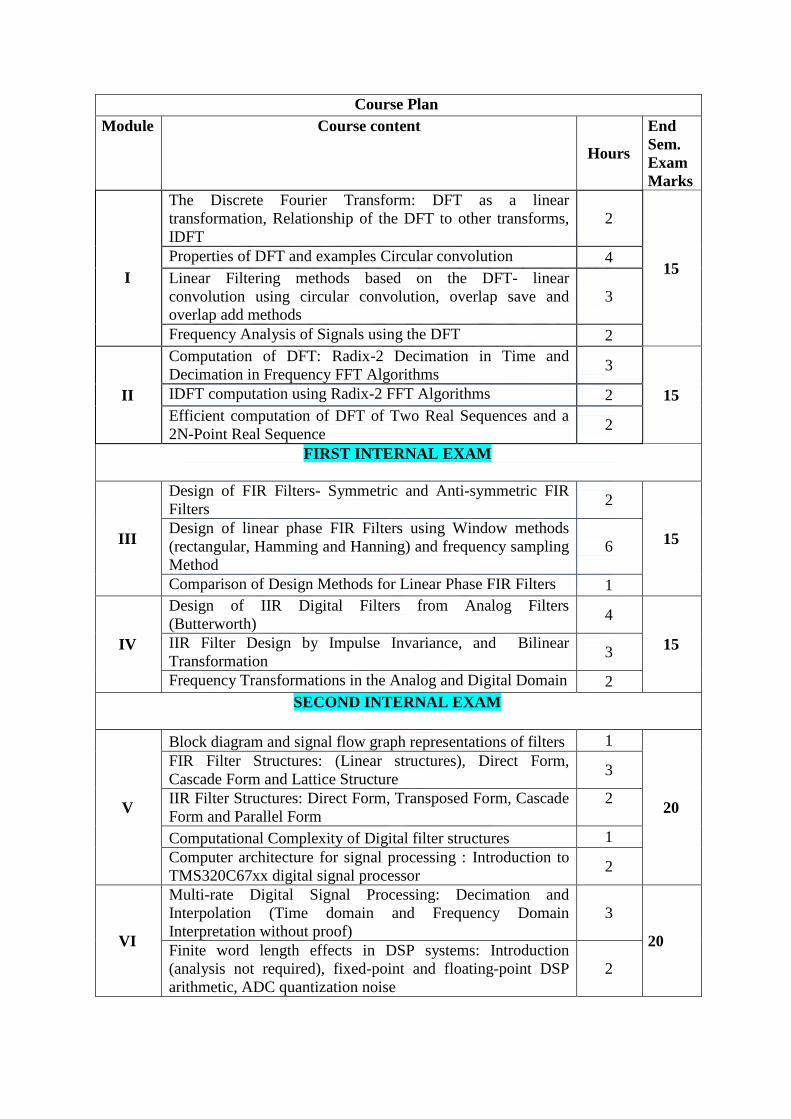
Course Plan
Module Course content
Hours
End
Sem.
Exam
Marks
I
The Discrete Fourier Transform: DFT as a linear
transformation, Relationship of the DFT to other transforms,
IDFT
2
15 Properties of DFT and examples Circular convolution 4
Linear Filtering methods based on the DFT- linear
convolution using circular convolution, overlap save and
overlap add methods
3
Frequency Analysis of Signals using the DFT 2
II
Computation of DFT: Radix-2 Decimation in Time and
Decimation in Frequency FFT Algorithms 3
15 IDFT computation using Radix-2 FFT Algorithms 2
Efficient computation of DFT of Two Real Sequences and a
2N-Point Real Sequence 2
FIRST INTERNAL EXAM
III
Design of FIR Filters- Symmetric and Anti-symmetric FIR
Filters 2
15 Design of linear phase FIR Filters using Window methods
(rectangular, Hamming and Hanning) and frequency sampling
Method
6
Comparison of Design Methods for Linear Phase FIR Filters 1
IV
Design of IIR Digital Filters from Analog Filters
(Butterworth) 4
15 IIR Filter Design by Impulse Invariance, and Bilinear
Transformation 3
Frequency Transformations in the Analog and Digital Domain 2
SECOND INTERNAL EXAM
V
Block diagram and signal flow graph representations of filters 1
20
FIR Filter Structures: (Linear structures), Direct Form,
Cascade Form and Lattice Structure 3
IIR Filter Structures: Direct Form, Transposed Form, Cascade
Form and Parallel Form
2
Computational Complexity of Digital filter structures 1
Computer architecture for signal processing : Introduction to
TMS320C67xx digital signal processor 2
VI
Multi-rate Digital Signal Processing: Decimation and
Interpolation (Time domain and Frequency Domain
Interpretation without proof)
3
20 Finite word length effects in DSP systems: Introduction
(analysis not required), fixed-point and floating-point DSP
arithmetic, ADC quantization noise
2

Finite word length effects in IIR digital filters: coefficient
quantization errors 2
Finite word length effects in FFT algorithms: Round off errors 2
END SEMESTER EXAM
Question Paper Pattern (End Sem Exam)
Maximum Marks: 100 Time : 3 hours
The question paper shall consist of three parts. Part A covers modules I and II, Part B covers
modules III and IV, and Part C covers modules V and VI. Each part has three questions
uniformly covering the two modules and each question can have maximum four subdivisions.
In each part, any two questions are to be answered. Mark patterns are as per the syllabus with
40 % for theory and 60% for logical/numerical problems, derivation and proof.

COURSE
CODE COURSE NAME L-T-P-C
YEAR OF
INTRODUCTION
EC303 Applied Electromagnetic Theory 3-0-0-3 2016
Prerequisite: Nil
Course objectives:
1. To introduce basic mathematical concepts related to electromagnetic vector fields.
2. To impart knowledge on the basic concepts of electric and magnetic fields
3. To develop a solid foundation in the analysis and application of electromagnetic fields,
Maxwell’s equations and Poynting theorem.
4. To become familiar with propagation of signal through transmission lines and
waveguides.
Syllabus:
Co-ordinate transformation, vector algebra, vector calculus, electrostatics, magneto statics,
Maxwell’s equations, Boundary condition, Solution of wave equation, propagation of plane
EM wave in different media, Poynting vector theorem, transmission lines, Smith chart,
Waveguides.
Expected outcome:
At the end of the course, students will be able:
1. To develop a solid foundation and a fresh perspective in the analysis and application of
electromagnetic fields.
2. To analyse the propagation of electromagnetic waves in different media.
3. To analyze the characteristics of transmission lines.
4. To solve the different transmission line problems using Smith chart
5. To understand the different modes of propagation in waveguides.
Text Books:
1. John D. Kraus, Electromagnetics, 5/e, TMH, 2010.
2. Mathew N O Sadiku, Elements of Electromagnetics, Oxford University Press, 6/e, 2014.
3. William, H., Jf Hayt, and John A. Buck. Engineering Electromagnetics. McGraw-Hill,
8/e McGraw-Hill, 2014.
References:
1. Jordan and Balmain , Electromagnetic waves and Radiating Systems, PHI, 2/e,2013
2. Joseph A Edminister , Electromagnetics, Schaum‘s Outline Series McGraw Hill, 4/e,
1995
3. Martin A Plonus , Applied Electromagnetics, McGraw Hill, 2/e,1978.
4. Matthew N.O. Sadiku & S.V. Kulkarni "‘Principles of Electromagnetics’, Oxford
University Press Inc. Sixth Edition, Asian Edition,2015
5. Nannapaneni Narayana Rao, Elements of Engineering Electromagnetics, Pearson, 6/e,
2006.
6. Umran S. Inan and Aziz S. Inan, Engineering Electromagnetics, Pearson, 2010.

Course Plan
Module Course content
Hours
End
Sem.
Exam
Marks
I
Review of vector calculus, Spherical and Cylindrical
coordinate system, Coordinate transformation 1
0 Curl, Divergence, Gradient in spherical and cylindrical
coordinate system. 1
Electric field – Application of Coulomb’s law, Gauss law and
Amperes current law (proof not required, simple problems
only)
1
15
Poisson and Laplace equations (proof not required, simple
problems only), Determination of E and V using Laplace
equation.
1
Derivation of capacitance and inductance of two wire
transmission line and coaxial cable. Energy stored in Electric
and Magnetic field.
2
Displacement current density, continuity equation. Magnetic
vector potential. Relation between scalar potential and vector
potential.
2
II
Maxwell’s equation from fundamental laws. 1
15
Boundary condition of electric field and magnetic field from
Maxwell's equations 1
Solution of wave equation 1
Propagation of plane EM wave in perfect dielectric, lossy
medium, good conductor, media-attenuation, phase velocity,
group velocity, skin depth.
3
FIRST INTERNAL EXAM
III
Reflection and refraction of plane electromagnetic waves at
boundaries for normal & oblique incidence (parallel and
perpendicular polarization), Snell’s law of refraction,
Brewster angle.
4
15 Power density of EM wave, Poynting vector theorem,
Complex Poynting vector. 3
Polarization of electromagnetic wave-linear, circular and
elliptical polarisation. 2
IV
Uniform lossless transmission line - line parameters 1
15 Transmission line equations, Voltage and Current distribution
of a line terminated with load 2
Reflection coefficient and VSWR. Derivation of input
impedance of transmission line. 2
SECOND INTERNAL EXAM
V
Transmission line as circuit elements (L and C). 2
20 Half wave and quarter wave transmission lines. 1
Development of Smith chart - calculation of line impedance
and VSWR using smith chart. 2

Single stub matching (Smith chart and analytical method). 2
VI
Parallel-Plate Waveguide - TE & TM waves. 1
20
The hollow rectangular wave guide – modes of propagation of
wave- dominant mode, group velocity and phase velocity -
derivation and simple problems only.
3
Attenuation in wave guides, guide wavelength and impedance
-derivation and simple problems only. 3
END SEMESTER EXAM
Question Paper (End semester exam)
Maximum marks : 100 Time: 3 hours
The question paper shall consist of three parts. Part A covers modules I and II, Part B covers
modules III and IV, and Part C covers modules V and VI. Each part has three questions
uniformly covering the two modules and each question can have maximum four subdivisions.
In each part, any two questions are to be answered. Mark patterns are as per the syllabus with
50 % for theory and 50% for logical/numerical problems, derivation and proof.

COURSE
CODE COURSE NAME L-T-P-C
YEAR OF
INTRODUCTION
EC305 Microprocessor & Microcontroller 3-0-0-3 2016
Prerequisite: EC207 Logic Circuit Design
Course objectives:
1. To understand fundamental operating concepts of microprocessors and microcontrollers.
2. To communicate with various devices using controller.
3. To design a microcontroller based system with the help of the interfacing devices.
4. To program the controller to make various peripherals work for specified application.
Syllabus:
Microprocessors: 8085 architecture and its operation, microprocessor initiated operations
and bus organization, pin configuration and functions, generation of control signals for
external operations- fetch, IO/M, read/write, machine cycles and bus timings. Addressing
modes, instruction set, instruction classification. Overview/concept of peripheral IC
interfacing with 8085 microprocessor (8251, 8253, 8255, 8279). Simple examples in
assembly language programming for 8085 (only for internal examination). Introduction to
development tools: IDE, cross assembler, builder, linker and debugger.( not required for
exam). Introduction to 8086 and comparison between 8086, 80286, 80386, 80486 and
Pentium.
Microcontrollers: 8051- features, architecture, memory organization, registers, I/O ports, pin
configuration and functions. Addressing modes, instruction set, instruction classification.
Assembly language programming. Interrupts in 8051. Timer/Counter programming:
Operating modes, time delay generation, Waveform generation. Serial communication: RS
232 interface, registers in UART, modes of operation, programming examples for serial data
transmission and reception. Interfacing of DIP switch, stepper motor, ADC, DAC, LEDs and
seven segment displays, alphanumeric LCD module with 8051.
Expected outcome:
The students will be able to:
1. Distinguish various types of processor architectures.
2. Describe architectures, memory organization of 8085 microprocessor and 8051.
3. Develop programming skills in assembly for interfacing peripheral devices with 8051
Text Books:
1. Kenneth J. Ayala, The 8051 Microcontroller, Cengage learning, 3/e.
2. Lyla B.Das : Microprocessors and Microcontrollers, Pearson Education, India, 2011
3. Ramesh S. Goankar. 8085 Microprocessors Archiecture Application and
Programming. Penram International, 5/e.
References:
1. Aditya P Mathur, Introduction to Microprocessor. Tata Mc Graw – Hill
2. Han Way Hung, “PIC Microcontroller, An introduction to software and hardware
interfacing “, Cenage learning.
3. I.Scott Mackenzie, Raphel C.-W Phan, The 8051 microcontroller, 4th
edition.
4. Muhammed Ali Mazidi, The 8051 Microcontroller and Embedded Systems, Pearson
Education, 2nd
edition
5. Nagoorkani, Microprocessors and Microcontrollers 2e, McGraw Hill Education India,
2012.
6. Soumitra Kumar Mandal. Microprocessors and Microcontrollers Architecture,
Programming & Interfacing Using 8085, 8086 and 8051, McGraw Hill Education
(2011).
7.

Course Plan
Module Course content
Hours
End
Sem.
Exam
Marks
I
Microprocessors: Introduction, organization of a
microprocessor based system, evolution of microprocessors,
8085 architecture and its operation, microprocessor initiated
operations and bus organization, pin configuration and
functions, generation of control signals for external operations-
fetch, IO/M, read/write.
5 15
II
Machine cycles and bus timings, Addressing modes, instruction
set instruction classification. 4
15 Overview/concept of peripheral IC interfacing with 8085
microprocessor (8251, 8253, 8255, 8279). 3
Simple examples in assembly language programming for 8085
(only for internal examination) 2
0 Introduction to development tools: IDE, cross assembler,
builder, linker and debugger.( not required for exam) 3
FIRST INTERNAL EXAM
III
Introduction to 8086 and comparison between
8086,80286,80386,80486 and Pentium 2
15 Microcontrollers: Introduction, comparison between
microprocessors and microcontrollers, microcontroller families,
8051- features, architecture, memory organization, registers,
I/O ports, pin configuration and functions.
6
IV Addressing modes, instruction set, instruction classification. 2
15 Assembly language programming examples for 8051. 3
SECOND INTERNAL EXAM
V
Interrupts in 8051: Types, interrupt source, interrupt handling
and programming 2
20
Timer/Counter programming: Operating modes, time delay
generation, Waveform generation. 2
Serial communication: RS 232 interface, registers in UART,
modes of operation, programming examples for serial data
transmission and reception
2
VI
Interfacing: Interfacing (block schematic and assembly
language programming) of DIP switch, stepper motor, ADC,
DAC, LEDs and seven segment displays, alphanumeric LCD
module with 8051.
6 20
END SEMESTER EXAM
Question Paper Pattern (End semester exam)
Max. Marks: 100 Time: 3 hours
The question paper shall consist of three parts. Part A covers modules I and II, Part B covers
modules III and IV, and Part C covers modules V and VI. Each part has three questions
uniformly covering the two modules and each question can have maximum four subdivisions.
In each part, any two questions are to be answered. Mark patterns are as per the syllabus with
80 % for theory and 20% for logical/numerical problems and programming.

COURSE
CODE COURSE NAME L-T-P-C
YEAR OF
INTRODUCTION
EC307 Power Electronics & Instrumentation 3-0-0-3 2016
Prerequisite: EC205 Electronic Circuits
Course objectives:
1. To provide an insight on the concepts of Power Electronics and Electronic instruments.
2. To study the applications of Power electronics such as Switched mode regulators and
inverters.
3. To develop understanding of the concept of Transducers and Digital instruments.
Syllabus:
Power semiconductor switches and its static and dynamic characteristics. Switched mode
regulators, SMPS, Switched mode inverters, UPS.
Performance characteristics of instruments, Measurement of passive components, Different
Transducers, Digital Instruments.
Expected outcome:
The students will be able:
1. To understand the concepts of Power Electronics and the various applications.
2. To get an insight on various electronic instruments, their configuration and
measurements using them.
3. To understand the principle of operation of Transducers
Text Books:
1. Bell D. A., Electronic Instrumentation and Measurements, Oxford University Press,
2003.
2. Rashid M. H., "Power Electronics Circuits, Devices and Applications”, Prentice Hall
India, Third Edition, New Delhi.
3. Umanand L., Power Electronics Essentials and Applications, Wiley India, 2015.
References:
1. Daniel W. Hart, Power Electronics, McGraw Hill, 2011.
2. Doeblin E., Measurement Systems, 5/e, McGraw Hill, 2003.
3. Helfrick A. D. and W. D. Cooper: Modern Electronic Instrumentation and Measurement
Techniques, 5/e, PHI, 2003.
4. Mandal, Power Electronics 1e, McGraw Hill Education India, 2014
5. Mohan N. and T. M. Undeland, Power Electronics: Converters, Applications and Design,
John Wiley, 2007.
6. Nakra, Instrumentation, Measurement and Analysis,4e, Mc Graw –Hill Education New
Delhi,2016
7. Patranabis D., Principles of Electronic Instrumentation, PHI, 2008.

Course Plan
Module Course content
Hours
End
Sem.
Exam
Marks
I
Linear Electronics versus Power Electronics - Power
semiconductor switches. 1
15
Power diodes-structure, static and dynamic characteristics 2
Power transistors - Power BJT, Power MOSFET, GTO and
IGBT 3
Steady state and switching characteristics of Power BJT, Power
MOSFET and IGBT. 2
II
Introduction to Switched mode regulators 1
15
Buck, Boost and Buck-Boost DC-DC converters 2
Waveforms and expression of DC-DC converters for output
voltage, voltage and current ripple under continuous conduction
mode. (Derivation not required)
1
Isolated converters - Flyback, Forward, Push Pull, Half Bridge
and Full Bridge Converters - waveforms and governing
equations. (Derivation not required)
3
FIRST INTERNAL EXAM
III
Overview of SMPS, Switched mode inverters- Principles of
PWM switching schemes. 2
15 Single phase inverters - half bridge, full bridge and push pull. 2
UPS - on line and off line. 1
Three phase inverters - PWM and Space vector modulation in
three phase inverters. 3
IV
Generalized configurations of instruments - Functional
elements. Classification of instruments 1
15
Generalized performance characteristics of instruments - Static
characteristics and Dynamic characteristics. 2
Measurement of: resistance using Wheastone’s bridge,
inductance using Maxwell-Wien bridge, and capacitance using
Schering’s bridge.
2
SECOND INTERNAL EXAM
V
Transducers - Classification, Selection of transducers. 1
20
Resistance transducers - Principle of operation, strain gauge. 2
Inductive Transducers: LVDT. 2
Capacitive transducers - different types, capacitor microphone,
Hall Effect transducer, proximity transducers. 2
VI
Electronic Multimeter, Audio Power Meter, RF power meter 2
20 Digital Instruments - Basics, digital measurement of time,
phase, frequency and digital voltmeter. 2
Frequency synthesizer, Spectrum analyzers, Logic State
analyzers (block diagram only). 1

Digital storage oscilloscope – Working Principle, controls and
applications. 2
END SEMESTER EXAM
Question Paper Pattern ( End Sem Exam)
Max. Marks: 100 Time: 3 hours
The question paper shall consist of three parts. Part A covers modules I and II, Part B covers
modules III and IV, and Part C covers modules V and VI. Each part has three questions
uniformly covering the two modules and each question can have maximum four subdivisions.
In each part, any two questions are to be answered. Mark patterns are as per the syllabus with
100 % for theory.

COURSE
CODE COURSE NAME L-T-P-C
YEAR OF
INTRODUCTION
EC333 Digital Signal Processing Lab 0-0-3-1 2016
Prerequisite:
EC 213 Electronics Design Automation Lab, EC 202 Signals & Systems
Course objectives:
To enable the students to explore the concepts of design, simulation and implementation
of various systems using MATLAB/SciLab/OCTAVE and DSP kit.
List of Experiments:
Part A: Experiments on Digital Signal Processor/ DSP kits: (All experiments are
mandatory)
1. Generation of sine wave and standard test signals.
2. Convolution : Linear and Circular
3. Real Time FIR Filter implementation (Low-pass, High-pass and Band-pass) by
inputting a signal from the signal generator
4. Real Time IIR Filter implementation ( Low-pass, High-pass and Band-pass) by
inputting a signal from the signal generator
5. Sampling of analog signal and study of aliasing.
Part B: Experiments based on MATLAB/SciLab/OCTAVE (7 experiments are
mandatory)
1. Generation of Waveforms (Continuous and Discrete)
2. Verification of Sampling Theorem.
3. Time and Frequency Response of LTI systems (First and second order).
4. Linear Convolution, Circular Convolution and Linear Convolution using Circular
Convolution.
5. To find the DFT and IDFT for the given input sequence.
6. Linear convolution using DFT (Overlap-add and Overlap-Save methods).
7. To find the DCT and IDCT for the given input sequence.
8. To find FFT and IFFT for the given input sequence.
9. FIR and IIR filter design using Filter Design Toolbox.
10. FIR Filter (Low-pass, High-pass and Band-pass)design (Window method).
11. IIR Filter (Low-pass, High-pass and Band-pass)design (Butterworth and Chebychev).
12. Generation of AM, FM & PWM waveforms and their spectrum.
13. Generation of DTMF signal.
14. Study of sampling rate conversion (Decimation, Interpolation, Rational factor).
15. Filtering of noisy signals
16. Implementation of simple algorithms in audio processing (delay, reverb, flange etc.).
17. Implementation of simple algorithms in image processing (detection, de-noising,
filtering etc.)
Expected outcome:
The students will be able to:
Design, simulate and realize various systems related to DSP.

COURSE
CODE COURSE NAME L-T-P-C
YEAR OF
INTRODUCTION
EC335 Power Electronics & Instrumentation Lab 0-0-3-1 2016
Prerequisite: NIL
Course objectives:
To design and implement basic power electronic circuits
To study the working of transducers
To train the usage of Digital Instruments
List of Experiments (8 experiments mandatory):
Cycle I (Four mandatory)
1. Design and Set up DC-DC converter
2. Design and Set up Push pull DC- DC Converter
3. Design and Set up Buck DC-DC Converters
4. Design and Set up Simple SMPS
5. Design and Set up Half bridge and full bridge converters
6. Design and Set up basic Inverter Circuits
Cycle II (Four mandatory)
7. Transducer measurements using diode thermometer
8. Transducer measurements using LVDT
9. Transducer measurements using Strain gauge.
10. Transducer measurements using Pressure transducer.
11. Transducer measurements using Thermocouple & RTDS
12. Transducer measurements using Photocells
Desired Experiment
13. Study of Digital LCR meter, Frequency synthesizer, Spectrum analyzer and Logic State
analyzer application.
Expected outcome:
The students will be able to:
1. Design and demonstrate basic power electronic circuits.
2. Use transducers for application.
3. Function effectively as an individual and in a team to accomplish the given task.

COURSE
CODE COURSE NAME L-T-P-C
YEAR OF
INTRODUCTION
EC360 Soft Computing 3-0-0 -3 2016
Prerequisite: NIL
Course objectives:
1. To familiarize various components of soft computing like fuzzy logic, neural networks
and genetic algorithm.
2. To give an overview of fuzzy Logic and to understand the concepts and terminologies of
fuzzy systems
3. To give a description on artificial neural networks with its advantages and application.
4. To study the fundamentals of Genetic Algorithm (GA).
5. To understand the concepts of hybrid systems.
Syllabus:
Fuzzy sets and systems. Neural Networks - Applications - typical architecture, pattern
Classification and pattern Association. Fundamentals of Genetic Algorithm, AI search
algorithm and hybrid structure.
Expected outcome:
The students will be able to:
1. Identify and describe soft computing techniques and their roles in building intelligent
Machines.
2. Apply fuzzy logic and reasoning to handle uncertainty and solve engineering problems
3. Recognize the feasibility of applying a soft computing methodology for a particular
Problem.
4. Apply neural networks to pattern classification and regression problems.
5. Apply genetic algorithms to combinatorial optimization problems
Text Books:
1. D.E. Goldberg, "Genetic Algorithms: Search, Optimization and Machine Learning",
Addison Wesley,N.Y, 1989.
2. Laurene V. Fausett, (1993) “Fundamentals of Neural Networks: Architecture,
Algorithms and Applications", Prentice Hall.
3. Timothy J. Ross, “Fuzzy Logic with Engineering Applications” Wiley India.
References:
1. Ibrahim A. M., Introduction to Applied Fuzzy Electronics, PHI, 2013.
2. J. Yen and R. Langari, Fuzzy Logic, Intelligence, Control and Information, Pearson
Education.
3. K.H.Lee, First Course on Fuzzy Theory and Applications, Springer-Verlag.
4. Lin C. T. and C.S. G. Lee, Neural Fuzzy Systems, Prentice Hall, 1996.
5. S. Rajsekaran & G.A. Vijayalakshmi Pai, “Neural Networks, Fuzzy Logic and Genetic
Algorithm: Synthesis and Applications” Prentice Hall of India.
6. S.N. Sivanandan and S.N. Deepa, Principles of Soft Computing, Wiley India, 2007.
ISBN: 10: 81-265-1075-7.

Course Plan
Module Course content
Hours
End
Sem.
Exam
Marks
I
Soft computing: Introduction, soft computing vs hard
computing, Fuzzy Computing, Neural Computing, Genetic
Algorithms. applications of soft computing
2
15 Introduction to fuzzy sets and systems-crispness, vagueness,
uncertainty and fuzziness. Basics of fuzzy sets, membership
functions, support of a fuzzy set height, normalized fuzzy set,
alpha cuts.
3
II
Type- 2 fuzzy sets. Operation on fuzzy set-complement,
intersection, union, Demorgan's Law Equality & subset hood. 4
15 Extension Principle and its application, Fuzzy relation-
operations, projection, max-min, min-max composition,
cylindrical extension.
3
FIRST INTERNAL EXAM
III
Reflexivity, symmetry and transitivity of fuzzy relations. Fuzzy
prepositions, fuzzy connectives, linguistic variables, hedges. 4
15 Approximate reasoning or fuzzy inference, Fuzzy rule based
system. Fuzzification and defuzzification using centroid, centre
of sums.
4
IV
Introduction to Neural Networks - Applications –Biological
neuron- Typical architecture of Artificial Neural Networks -
Common activation function.
4
15
McCulloh Pitts Neuron – Architecture, logic implementatons.
Supervised and Unsupervised learning 4
SECOND INTERNAL EXAM
V
Linear Separability, Pattern Classification: Perceptrons 2
20 Back propagation network and its architecture, Back
propagation learning, back propagation algorithm 4
VI
Genetic Algorithm Basic concepts, Initialization and selection,
Survival of the Fittest - Fitness Computations. 5
20 Operators - Cross over, Mutation. 3
END SEMESTER EXAM
Question Paper ( End semester exam)
Max. Marks: 100 Time : 3 hours
The question paper shall consist of three parts. Part A covers modules I and II, Part B covers
modules III and IV, and Part C covers modules V and VI. Each part has three questions
uniformly covering the two modules and each question can have maximum four subdivisions.
In each part, any two questions are to be answered. Mark patterns are as per the syllabus
with 50 % for theory, derivation, proof and 50% for logical/numerical problems.

COURSE
CODE COURSE NAME L-T-P-C
YEAR OF
INTRODUCTION
EC361 Digital System Design 3-0-0-3 2016
Prerequisite: EC207 Logic Circuit Design
Course objectives:
1. To study synthesis and design of CSSN
2. To study synthesis and design of ASC
3. To study hazards and design hazard free circuits
4. To study PLA folding
1. To study architecture of one CPLDs and FPGA family
Syllabus: Clocked synchronous networks, asynchronous sequential circuits, Hazards, Faults, PLA,
CPLDs and FPGA
Expected outcome:
The student will be able:
1. To analyze and design clocked synchronous sequential circuits
2. To analyze and design asynchronous sequential circuits
3. To apply their knowledge in diagnosing faults in digital circuits, PLA
4. To interpret architecture of CPLDs and FPGA
Text Books:
1. Donald G Givone, Digital Principles & Design, Tata McGraw Hill, 2003
2. John F Wakerly, Digital Design, Pearson Education, Delhi 2002
3. John M Yarbrough, Digital Logic Applications and Design, Thomson Learning
References:
1. Miron Abramovici, Melvin A. Breuer and Arthur D. Friedman, Digital Systems Testing
and Testable Design, John Wiley & Sons Inc.
2. Morris Mano, M.D.Ciletti, Digital Design, 5th
Edition, PHI.
3. N. N. Biswas, Logic Design Theory, PHI
4. Richard E. Haskell, Darrin M. Hanna , Introduction to Digital Design Using Digilent
FPGA Boards, LBE Books- LLC
5. Samuel C. Lee, Digital Circuits and Logic Design, PHI
6. Z. Kohavi, Switching and Finite Automata Theory, 2nd
ed., 2001, TMH
Course Plan
Module Course content
Hours
End
Sem.
Exam
Marks
I
Analysis of clocked Synchronous Sequential Networks(CSSN) 2
15
Modelling of CSSN – State assignment and reduction 1
Design of CSSN 2
Iterative circuits 1
ASM Chart and its realization 2
II
Analysis of Asynchronous Sequential Circuits (ASC) 2
15
Flow table reduction- Races in ASC 1
State assignment problem and the transition table- Design of
AS 2
Design of Vending Machine controller. 2

FIRST INTERNAL EXAM
III
Hazards – static and dynamic hazards – essential 1
15
Design of Hazard free circuits – Data synchronizers 1
Mixed operating mode asynchronous circuits 1
Practical issues- clock skew and jitter 1
Synchronous and asynchronous inputs – switch bouncing 2
IV
Fault table method – path sensitization method – Boolean
difference method 2
15 Kohavi algorithm 2
Automatic test pattern generation – Built in Self Test(BIST) 3
SECOND INTERNAL EXAM
V
PLA Minimization - PLA folding 2
20 Foldable compatibility Matrix- Practical PLA 2
Fault model in PLA 1
Test generation and Testable PLA Design. 3
VI
CPLDs and FPGAs - Xilinx XC 9500 CPLD family, functional
block diagram– input output block architecture - switch matrix 3
20 FPGAs – Xilinx XC 4000 FPGA family – configurable logic
block - input output block, Programmable interconnect 3
END SEMESTER EXAM
Question Paper Pattern ( End semester exam)
Max. Marks: 100 Time : 3 hours
The question paper shall consist of three parts. Part A covers modules I and II, Part B covers
modules III and IV, and Part C covers modules V and VI. Each part has three questions
uniformly covering the two modules and each question can have maximum four subdivisions.
In each part, any two questions are to be answered. Mark patterns are as per the syllabus with
50 % for theory, derivation, proof and 50% for logical/numerical problems.

COURSE
CODE COURSE NAME L-T-P-C
YEAR OF
INTRODUCTION
EC363 Optimization Techniques 3-0-0-3 2016
Prerequisite: NIL
Course objectives:
1. To understand the need and origin of the optimization methods.
2. To get a broad picture of the various applications of optimization methods used in
engineering.
3. To define optimization problem and its various components
Syllabus: Engineering applications of optimization, Formulation of design problems as
mathematical programming problems, objective function, constraints, classification of
optimization problems/techniques, necessary and sufficient conditions for optimality, uni-
modality, convexity, Mathematical formulation of LP Problems, Reduction of a LPP to the
standard form. Feasible solutions, Graphical solution methods, optimality conditions,
degeneracy, Simplex algorithm, Duality in linear programming, Transportation Problem,
Game theory, Network path models, Nonlinear unconstrained optimization, Modern methods
of optimization, Genetic algorithm. Introduction to optimization tools and software.
Expected outcome:
The students will (i) have a thorough understanding of optimization techniques
(ii)l be able to formulate and solving the engineering optimization problems
Text Books:
1. H.A. Taha, “ Operations Research”, 5/e, Macmillan Publishing Company, 1992.
2. Kalynamoy Deb. “Optimization for Engineering Design‐ Algorithms and Examples”,
Prentice‐Hall of India Pvt. Ltd., New Delhi
3. Singiresu S Rao, “Engineering optimization Theory and Practice”, New Age
International, 2009
References:
1. A. Ravindran, D. T. Phillips, J. J. Solberg, Operations Research – Principles and
Practice, John Wiley and Sons.
2. Ashok D Belegundu, Tirupathi R Chandrupatla, “Optimization concepts and Application
in Engineering”, Pearson Education.
3. Hadley, G. “Linear programming”, Narosa Publishing House, New Delhi
4. J. S. Arora, Introduction to Optimum Design, McGraw-Hill Book Company.
5. Kanti Swarup, P.K.Gupta and Man Mohan, Operations Research, Sultan Chand and
Sons
6. Papalambros & Wilde, Principles of Optimal Design, Cambridge University Press, 2008

Course Plan
Module Course content
Hours
End
Sem.
Exam
Marks
I
Introduction: Engineering applications of optimization,
Formulation of design problems as mathematical programming
problems, objective function, constraints, classification of
optimization problems/techniques.
2
15 Optimization techniques: Classical optimization, unconstrained
single and multivariable minimization- necessary and sufficient
conditions for optimality, uni-modality, convexity. 5
II
Linear programming problems-I: Mathematical formulation of
LP Problems, slack, surplus and artificial variables. Reduction
of a LPP to the standard form, feasible solutions. Graphical
solution method, simplex algorithm and solution using tabular
method, optimality conditions and degeneracy. Duality in linear
programming
7 15
FIRST INTERNAL EXAM
III
Transportation Problem: Formulation of transportation
problem, Basic feasible solution using different methods- East
West corner method, Vogel approximation method, Optimality
methods, MODI method, Unbalanced transportation problem
7 15
IV
Game Theory: Introduction, 2- person zero – sum game; Saddle
point; Mini-Max and Maxi-Min Theorems (statement only);
Graphical solution (2x n, m x 2 game), dominance property.
Network path Models: Tree Networks – Minimal Spanning
Tree - Prim’s Algorithm. Shortest path problems- solution
methods – Dijkstra’s Method.
7 15
SECOND INTERNAL EXAM
V
Nonlinear unconstrained optimization: Single variable
optimization methods- Fibonacci search method, Newton-
Raphson method.
Multi-variable methods- Hook-Jeeves pattern search method,
Cauchy’s (steepest descent) method.
7 20
VI
Modern methods of optimization: Introduction to Genetic
algorithm, Cross over, Mutation, Reproduction, Simple
examples of applications in electronics engineering
5 20
Introduction to optimization tools and softwares. Solution of
optimization Problems using MATLAB. 2 0
END SEMESTER EXAM

Question Paper Pattern ( End sem. Exam.)
Max. Marks: 100 Time : 3 hours
The question paper shall consist of three parts. Part A covers modules I and II, Part B covers
modules III and IV, and Part C covers modules V and VI. Each part has three questions
uniformly covering the two modules and each question can have maximum four subdivisions.
In each part, any two questions are to be answered. Mark patterns are as per the syllabus with
30 % for theory and 70% for logical/numerical problems, derivation and proof.


COURSE
CODE COURSE NAME L-T-P-C
YEAR OF
INTRODUCTION
EC365 Biomedical Engineering 3-0-0-3 2016
Prerequisite: Nil
Course objectives:
1. To introduce student to basic biomedical engineering technology
2. To understand the anatomy & physiology of major systems of the body in designing
equipment for medical treatments.
3. To impart knowledge about the principle and working of different types of bio-medical
electronic equipment/devices.
Syllabus:
Human body-overview, Physiological systems of body, Measurement of physiological
parameters, Assisting and therapeutic devices, Medical laboratory equipments, Telemetry in
patient care, Patient safety, Medical imaging system
Expected outcome:
The students will be able:
1. To understand diagnosis and therapy related equipments.
2. To understand the problem and identify the necessity of equipment for diagnosis and
therapy.
3. To understand the importance of electronics engineering in medical field.
4. To understand the importance of telemetry in patient care
Text Books:
1. K S Kandpur, “Hand book of Biomedical instrumentation”, Tata McGraw Hill 2nd e/d.
2. Leslie Cromwell, Fred J. Weibell, Erich A. Pfeiffer, Biomedical Instrumentation and
Measurements, PHI, 2nd Edition, 2004
References:
1. Barbara Christe, Introduction to Biomedical Instrumentation, Cambridge University
Press, 2008.
2. J. J. Carr, “Introduction to Biomedical Equipment Technology”, Pearson Education 4th
e/d.
3. John G Webster, “Medical Instrumentation application and design”, John Wiley 3rd
e/d.
4. Richard Aston, “Principle of Biomedical Instrumentation and Measurement”. Merrill
Education/Prentice Hall.
Course Plan
Module Course content
Hours
End
Sem.
Exam
Marks
I
Introduction to bio-medical instrumentation system, overview
of anatomy and physiological systems of the body. 1
15
Sources of bio-electric potential: Resting and action potential,
propagation of action potentials. Bioelectric potentials
examples (ECG, EEG, EMG, ERG, EOG, EGG, etc
introduction only.)
2
Electrode theory: Nernst relation
Bio potential electrodes: Microelectrodes, skin surface
electrodes, needle electrodes.
1
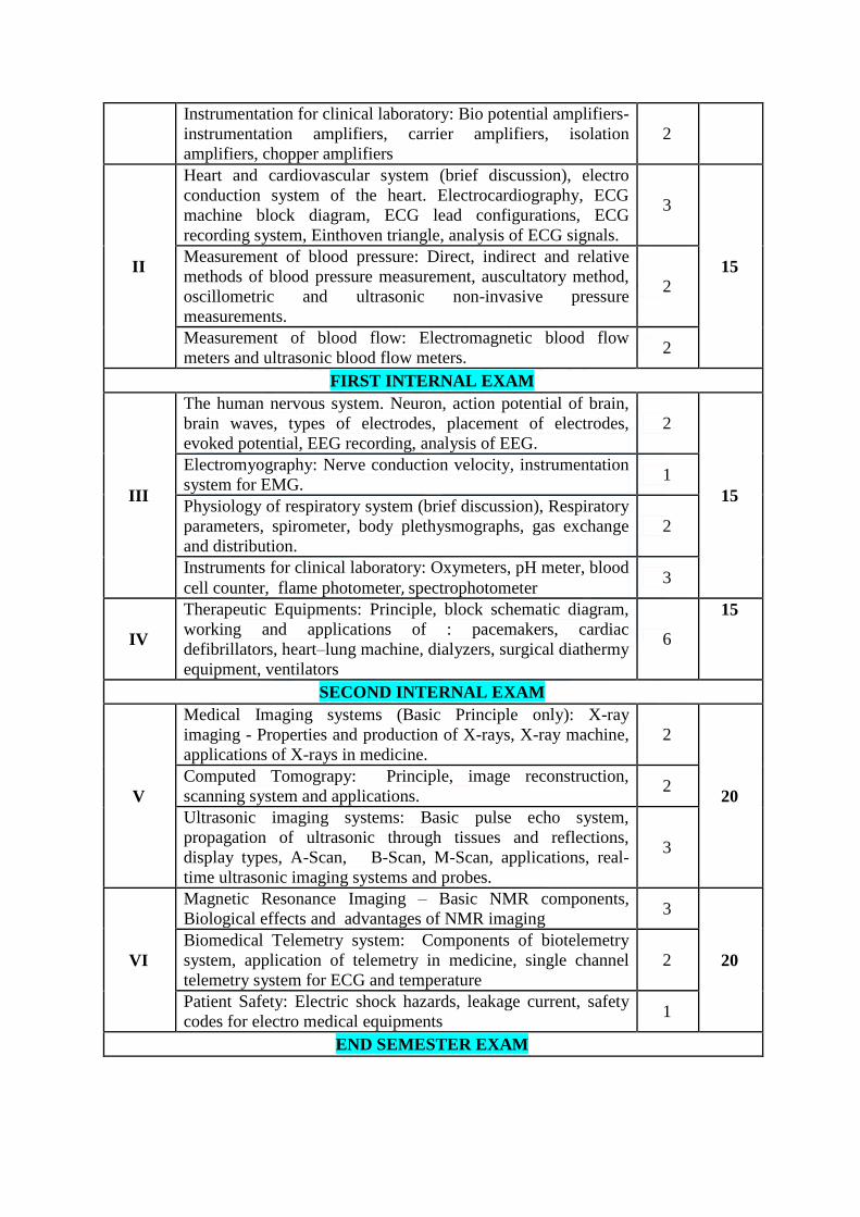
Instrumentation for clinical laboratory: Bio potential amplifiers-
instrumentation amplifiers, carrier amplifiers, isolation
amplifiers, chopper amplifiers
2
II
Heart and cardiovascular system (brief discussion), electro
conduction system of the heart. Electrocardiography, ECG
machine block diagram, ECG lead configurations, ECG
recording system, Einthoven triangle, analysis of ECG signals.
3
15 Measurement of blood pressure: Direct, indirect and relative
methods of blood pressure measurement, auscultatory method,
oscillometric and ultrasonic non-invasive pressure
measurements.
2
Measurement of blood flow: Electromagnetic blood flow
meters and ultrasonic blood flow meters. 2
FIRST INTERNAL EXAM
III
The human nervous system. Neuron, action potential of brain,
brain waves, types of electrodes, placement of electrodes,
evoked potential, EEG recording, analysis of EEG.
2
15
Electromyography: Nerve conduction velocity, instrumentation
system for EMG. 1
Physiology of respiratory system (brief discussion), Respiratory
parameters, spirometer, body plethysmographs, gas exchange
and distribution.
2
Instruments for clinical laboratory: Oxymeters, pH meter, blood
cell counter, flame photometer, spectrophotometer 3
IV
Therapeutic Equipments: Principle, block schematic diagram,
working and applications of : pacemakers, cardiac
defibrillators, heart–lung machine, dialyzers, surgical diathermy
equipment, ventilators
6
15
SECOND INTERNAL EXAM
V
Medical Imaging systems (Basic Principle only): X-ray
imaging - Properties and production of X-rays, X-ray machine,
applications of X-rays in medicine.
2
20
Computed Tomograpy: Principle, image reconstruction,
scanning system and applications. 2
Ultrasonic imaging systems: Basic pulse echo system,
propagation of ultrasonic through tissues and reflections,
display types, A-Scan, B-Scan, M-Scan, applications, real-
time ultrasonic imaging systems and probes.
3
VI
Magnetic Resonance Imaging – Basic NMR components,
Biological effects and advantages of NMR imaging 3
20
Biomedical Telemetry system: Components of biotelemetry
system, application of telemetry in medicine, single channel
telemetry system for ECG and temperature
2
Patient Safety: Electric shock hazards, leakage current, safety
codes for electro medical equipments 1
END SEMESTER EXAM
Question Paper Pattern ( End Sem. Exam)
Maximum Marks: 100 Time : 3 hours
The question paper shall consist of three parts. Part A covers modules I and II, Part B covers
modules III and IV, and Part C covers modules V and VI. Each part has three questions
uniformly covering the two modules and each question can have maximum four subdivisions.
In each part, any two questions are to be answered. Mark patterns are as per the syllabus with
100 % for theory.