course file contentskgr.ac.in/beta/wp-content/uploads/2018/09/ii-i-ec.pdf · design of transistor...
TRANSCRIPT

ELECTRONIC CIRCUITS
Poonam Swami, Assistant. Professor
COURSE FILE CONTENTS
S.N. Topics Page No.
1 Vision, Mission, PEO’s, & PO’s, PSOs
2 Syllabus (University Copy)
3 Course Objectives, Course Outcomes And Topic Outcomes
4 Course Prerequisites
5 CO’s, PO’s Mapping
6 Course Information Sheet (CIS)
a). Course Description
b). Syllabus
c). Gaps in Syllabus
d). Topics beyond syllabus
e). Web Sources-References
f). Delivery / Instructional Methodologies
g). Assessment Methodologies-Direct
h). Assessment Methodologies –Indirect
i). Text books & Reference books
7 Micro Lesson Plan
8 Teaching References Plan
9 Lecture Notes -Unit Wise (Hard Copy)
10 OHP/LCD SHEETS /CDS/DVDS/PPT (Soft/Hard copies)
11 University Previous Question papers
12 MID exam Descriptive Question Papers & Keys
13 MID exam Objective Question papers & Keys
14 Assignment topics with materials
15 Tutorial topics and Questions
16 Unit wise-Question bank
1 Two marks question with answers 5 questions
2 Three marks question with answers 5 questions
3 Five marks question with answers 5 questions
4 Objective question with answers 10 questions
5 Fill in the blanks question with answers 10 questions
17 Beyond syllabus Topics with material
18 Result Analysis-Remedial/Corrective Action
19 Sample Students Descriptive Answer sheets
20 Sample Students Assignment Sheets
21 Record of Tutorial Classes
22 Record of Remedial Classes
23 Record of guest lecturers conducted

ELECTRONIC CIRCUITS
Poonam Swami, Assistant. Professor
Part – 2
S.NO TOPICS
1 Attendance Register/Teacher Log Book
2 Time Table
3 Academic calendar
4 Continuous Evaluation – marks (Test, Assignments etc)
5 Status Report Internal Exams & Syllabus coverage
6 Teaching Dairy/Daily Delivery Record Micro lesson Plan
7 Continuous Evaluation – MID marks
8 Assignment Evaluation-marks/Grades
9 Special Descriptive Tests Marks
10 Sample students descriptive answer sheets
11 Sample students assignment sheets

ELECTRONIC CIRCUITS
Poonam Swami, Assistant. Professor
1. Vision, Mission, Program Educational Objectives (PEOs), Program
Outcomes (POs), Program Specific Outcomes (PSOs).
VISION
To be renowned department imparting both technical and non-technical skills to the students through
implementing new engineering pedagogy and research to produce competent new age electrical engineers.
MISSION
To transform the students into motivated and knowledgeable new age electrical engineers.
To advance the quality of education to produce world class technocrats with an ability to adapt to the
academically challenging environment.
To provide a progressive environment for learning through organized teaching methodologies,
contemporary curriculum and research in the thrust areas of electrical engineering.

ELECTRONIC CIRCUITS
Poonam Swami, Assistant. Professor
PROGRAM EDUCATIONAL OBJECTIVES (PEOs)
PEO-1: Apply knowledge and skills to provide solutions to Electrical and Electronics Engineering problems
in industry and governmental organizations or to enhance student learning in educational institutions
PEO-2: Work as a team with a sense of ethics and professionalism, and communicate effectively to manage
cross-cultural and multidisciplinary teams
PEO-3: Update their knowledge continuously through lifelong learning that contributes to personal, global
and organizational growth.

ELECTRONIC CIRCUITS
Poonam Swami, Assistant. Professor
PROGRAM OUTCOMES (POs)
PO-1: Engineering knowledge: Apply the knowledge of mathematics, science, engineering fundamentals
and an engineering specialization to the solution of complex engineering problems.
PO-2: Problem analysis: Identify, formulate, review research literature, and analyze complex engineering
problems reaching substantiated conclusions using first principles of mathematics, natural science and
engineering sciences.
PO-3: Design/development of solutions: design solutions for complex engineering problems and design
system components or processes that meet the specified needs with appropriate consideration for the public
health and safety, and the cultural, societal and environmental considerations.
PO-4: Conduct investigations of complex problems: use research based knowledge and research methods
including design of experiments, analysis and interpretation of data, and synthesis of the information to
provide valid conclusions.
PO-5: Modern tool usage: create, select and apply appropriate techniques, resources and modern engineering
and IT tools including prediction and modelling to complex engineering activities with an understanding of
the limitations.
PO-6: The engineer and society: apply reasoning informed by the contextual knowledge to assess societal,
health, safety, legal and cultural issues and the consequent responsibilities relevant to the professional
engineering practice.
PO-7: Environment sustainability: understand the impact of the professional engineering solutions in the
societal and environmental contexts, and demonstrate the knowledge of, and need for sustainable
development.
PO-8: Ethics: apply ethical principles and commit to professional ethics and responsibilities and norms of the
engineering practice.
PO-9: Individual and team work: function effectively as an individual and as a member or leader in diverse
teams, and in multidisciplinary settings.
PO-10: Communication: communicate effectively on complex engineering activities with the engineering
community and with society at large, such as, being able to comprehend and write effective reports and design
documentation, make effective presentations, and give and receive clear instructions.

ELECTRONIC CIRCUITS
Poonam Swami, Assistant. Professor
PO-11: Project management and finance: demonstrate knowledge and understanding of the engineering and
management principles and apply these to one’s own work, as a member and leader in a team, to manage
projects and in multidisciplinary environments.
PO-12: Lifelong learning: recognize the need for, and have the preparation and ability to engage in
independent and lifelong learning in the broader context of technological change.

ELECTRONIC CIRCUITS
Poonam Swami, Assistant. Professor
PROGRAM SPECIFIC OUTCOMES (PSOs)
PSO-1: Apply the engineering fundamental knowledge to identify, formulate, design & investigate complex
engineering problems of electric circuits, power electronics, electrical machines and power systems and to
succeed in competitive exams like GATE, IES, GRE,OEFL, GMAT, etc.
PSO-2: Apply appropriate techniques and modern engineering hardware and software tools in power systems
and power electronics to engage in life-long learning and to get an employment in the field of Electrical and
Electronics Engineering.
PSO-3: Understand the impact of engineering solutions in societal and environmental context, commit to
professional ethics and communicate effectively.
PSO- 4: Still to be defined.

ELECTRONIC CIRCUITS
Poonam Swami, Assistant. Professor

ELECTRONIC CIRCUITS
Poonam Swami, Assistant. Professor

ELECTRONIC CIRCUITS
Poonam Swami, Assistant. Professor
3) Course Objectives, Course Outcomes and Topic Outcomes
Course Objectives
1. To explain the operation, design and Analysis of single stage amplifiers using BJT and MOSFET.
2. To implement feedback amplifiers, large signal and oscillators.
3. To explain the operation of linear and non linear wave shaping circuits
4. To describe the switching characteristics of diode and transistor
Course Outcomes
After completion of this course the student is able to
Co1: Compare BJT and FET.
Co2: Describe feedback amplifiers and oscillators.
Co3: Define power amplifiers.
Co4: Sketch linear and nonlinear wave shape circuits.
Co5: State switching characteristics of diode and design multivibrators.

ELECTRONIC CIRCUITS
Poonam Swami, Assistant. Professor
Topic outcomes:
Sr.
No.
Topic Topic outcome At the end of the topic the
student will be able to
Unit-I
Single Stage Amplifiers
1 Introduction to BJT.
Define BJT
2 Introduction to FET.
Define FET
3 Two port device and network parameters. State Two port device and network
parameters.
4 Introduction to Single Stage Amplifiers:
Analysis of CE,CB,&CC Amplifiers Compare BJT and FET.
5 Analysis of FET
Discuss Analysis of FET
6 Analysis of FET
Discuss Analysis of FET
7 Classification of amplifiers Classify the amplifiers
8 Distortion in Amplifiers
State distortion in amplifier.
9 Comparison of CE, CB, CC Amplifiers Low
frequency Analysis, Distinguish CE, CB, CC amplifiers.
10 Low frequency response State low frequency response
11 Low frequency response of BJT Amplifiers Design Low frequency response of BJT
Amplifiers
12 Low frequency response of FET Amplifiers Design Low frequency response of FET
Amplifiers
13 Miller Effect Capacitance,
Discuss miller effect capacitance.
14 High frequency response of BJT Amplifiers Design high frequency response of BJT
Amplifiers
15 Square wave testing Explain square wave testing.
16 Revision of unit I Summarize single stage amplifiers.
Unit-II feedback Amplifiers
17 Concept of feedback Amplifiers, Define feedback amplifiers.
18 General characteristics of negative feedback
amplifiers State general characteristics of negative
feedback amplifiers
19 Effect of Feedback on Amplifier characteristics, Explain Effect of Feedback on Amplifier
characteristics

ELECTRONIC CIRCUITS
Poonam Swami, Assistant. Professor
20 Voltage series, voltage shunt feedback
configurations Identify voltage feedback
configurations.
21 Current series and current shunt Feedback
configurations Identify current feedback
configurations.
22 Illustrative problems Solve problems based on feedback
amplifier.
23 Oscillators: Conditions for oscillations
Define oscillators
24 Frequency and Amplitude Stability of
Oscillators, State stability condition for oscillation.
25 Generalized analysis of LC Oscillators Analysis of LC oscillators
26 Quartz oscillator Describe quartz oscillator
27 Hartley oscillator Describe Hartley oscillator.
28 Colpitts oscillator Describe colpitts oscillator.
29 RC –phase shift oscillator Describe RC phase shift oscillator.
30 Wein Bridge oscillators Describe wein bridge oscillator.
31 Revision of unit II Summarize feedback amplifiers and
oscillators.
Unit-III Large Signal Amplifiers:
32 Class A Power Amplifier, Sketch Class A Power Amplifier
33 Maximum Efficiency of Class –A amplifier calculate maximum Efficiency of Class
–A amplifier
34 Transformer Coupled Amplifier, Discuss transformer coupled amplifier.
35 Push Pull Amplifier complimentary Symmetry
Class-B Power Amplifier, Sketch Class B Power Amplifier
36 Phase Inverters, State phase inverters.
37 Transistor Power Dissipation, Define Transistor Power Dissipation.
38 Thermal Runway, Heat sinks Discuss thermal runway and heat
sinks.
39 CLASS C amplifier
Describe CLASS C amplifier
40 Revision of unit III Summarize large signal amplifiers.
Unit-IV Wave Shaping:

ELECTRONIC CIRCUITS
Poonam Swami, Assistant. Professor
41 High Pass RC Circuits their response for
Sinusoidal, Step, Pulse and Ramp Inputs. Examine High Pass RC Circuits their
response for Sinusoidal, Step, Pulse and
Ramp Inputs.
42 Low Pass RC Circuits their response for
Sinusoidal, Step, Pulse and Ramp Inputs. Examine Low Pass RC Circuits their
response for Sinusoidal, Step, Pulse and
Ramp Inputs
43 Clippers and Clampers: Diode Clippers,
Transistor Clippers, Define clippers and clampers.
44 Clipping at Two Independent levels Sketch Clipping at Two Independent
levels
45 Transfer Characteristics of Clippers, Define Transfer Characteristics of
Clippers
46 Comparators, Clamping Operation, State comparators, clampers.
47 Clamping Circuits using Diode with different
inputs, Design Clamping Circuits using Diode
with different inputs
48 Clamping Circuit Theorem Describe clamping circuit theorem.
49 Practical Clamping Circuit Design practical clamping circuits.
50 Revision of unit IV
Summarize wave shape circuits.
Unit-V Switching Characteristics of Devices
51 Diode as a Switch,
Discuss diode as a switch.
52 Piecewise Linear Diode Characteristics
State linear diode Characteristics
53 Transistor as a Switch,
Discuss transistor as a switch.
54 Breakdown Voltage Consideration of Transistor, Indicate Breakdown Voltage
Consideration of Transistor
55 Design of Transistor Switch,
Design of Transistor Switch
56 Transistor Switching Times.
Name Transistor Switching Times
57 Multi vibrators: Analysis and Design of Bi
stable multi vibrator Define multivibrators.
58 Mono stable Multi vibrators
Construct Mono stable Multi vibrators
59 A stable Multi vibrator
Construct A stable Multi vibrators
60 Schmitt Trigger using Transistors Construct Schmitt trigger using
multivibrators.
61 Revision of unit V Summarize Switching Characteristics of
Devices and multivibrator.
62 Revision of all units
Recall electronics circuit.

ELECTRONIC CIRCUITS
Poonam Swami, Assistant. Professor
4) COURSE PRE–REQUISITES
1. Basic of Mathematics. 2. Basic of semiconductor Devices. 3. Basic of two port network. 4. Basic of electrical network.

ELECTRONIC CIRCUITS
Poonam Swami, Assistant. Professor
5) CO’s, PO’s mapping
Course
Outcomes PO-I PO-II PO-III
PO-
IV PO-V
PO-
VI
PO-
VII
PO-
VIII
PO-
IX
PO-
X
PO-
XI
PO-
XII
CO-1 H M L - - - - - - - -
-
CO-2 M H L - - - - - - - -
-
CO-3 H M L - - - - - - - -
-
CO-4 L M H - - - - - - - -
-
CO-5 L M H - - - - - - - -
-
Legends:
L: low level
M: medium level
H: high level

ELECTRONIC CIRCUITS
Poonam Swami, Assistant. Professor
6. Course Information Sheet
6. a) COURSE DESCRIPTION:
PROGRAMME: B. Tech. (Electronics and
Communication Engineering.)
DEGREE: BTECH
COURSE: ELECTRONIC CIRCUITS YEAR: II SEM: ICREDITS: 3
COURSE CODE: EE305ES
REGULATION: R16
COURSE TYPE: CORE
COURSE AREA/DOMAIN: Design CONTACT HOURS: 4+1 (L+T)) hours/Week.
CORRESPONDING LAB COURSE CODE (IF ANY):
NIL
LAB COURSE NAME:
6. b) SYLLABUS:
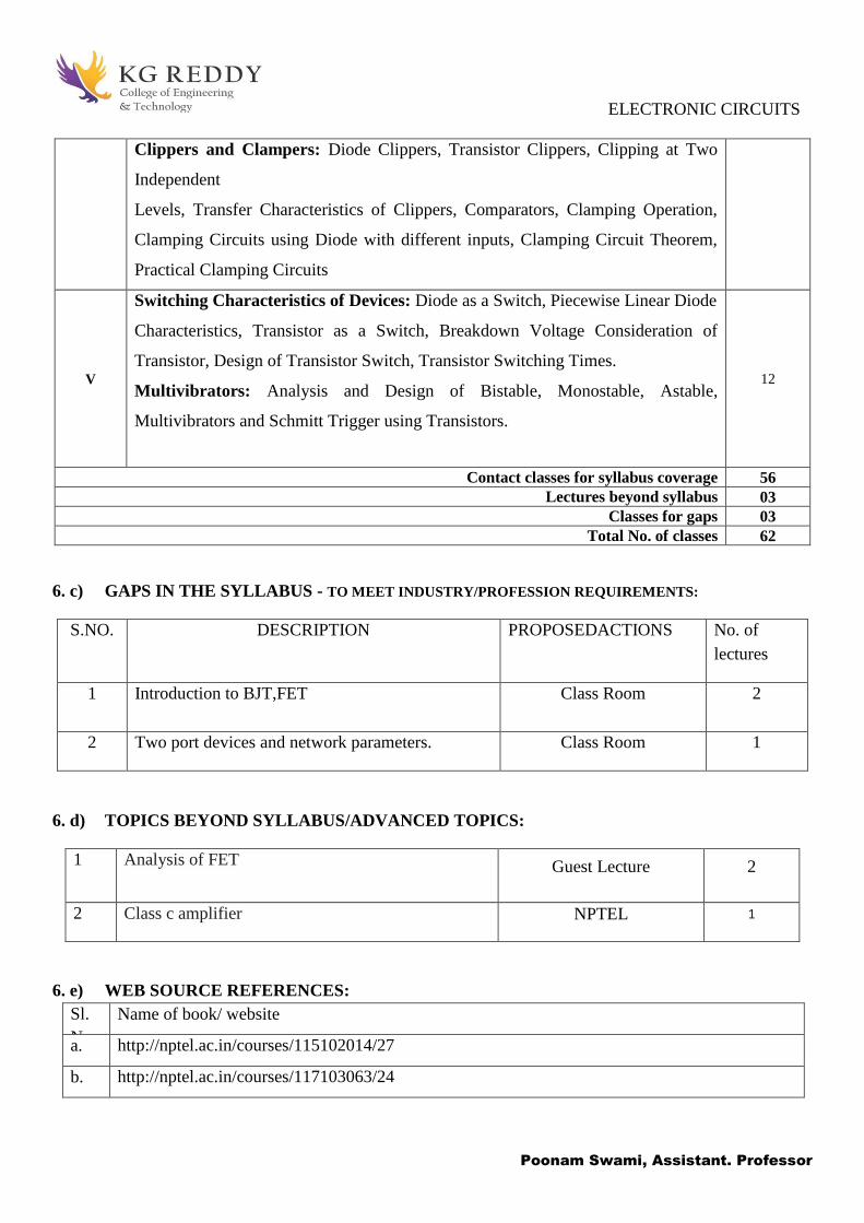
Unit Details Hours
I
Single Stage Amplifiers: Analysis of CE,CB,&CC Amplifiers Classification of
Amplifiers Distortion in Amplifiers, Comparison of CE, CB, CC Amplifiers Low
frequency Analysis, Low frequency response of BJT Amplifiers, Low frequency
response of FET Amplifiers Miller Effect Capacitance, High Frequency response
of BJT amplifiers, Square wave testing.
16
II
Feedback ampliers: Concept of feedback amplifiers, General Charachtertics of
negative feedback amplifiers, Effect of Feedback on Amplifier characteristics,
Voltage series, voltage Shunt, Current series and current shunt Feedback
configurations, Illustrative problems.
Oscillators: Conditions for oscillations, Frequency and Amplitude Stability of
Oscillators, Generalized analysis of LC Oscillators, Quartz, Hartley, and Colpitt’s
Oscillators, RC –phase Shift and Wein Bridge oscillators.
15
III
Large Signal Amplifiers: Class A Power Amplifier, Maximum Efficiency of
Class Amplifier, Transformer Coupled Amplifier, Push Pull Amplifier
complimentary Symmetry Class-B Power Amplifier, Phase Inverters, Transistor
Power Dissipation, Thermal Runway, Heat Sinks
09
IV
Wave Shaping: High Pass, Low Pass RC Circuits, their response for Sinusoidal,
Step, and Pulse and Ramp Inputs. 10
ELECTRONIC CIRCUITS
Poonam Swami, Assistant. Professor
Clippers and Clampers: Diode Clippers, Transistor Clippers, Clipping at Two
Independent
Levels, Transfer Characteristics of Clippers, Comparators, Clamping Operation,
Clamping Circuits using Diode with different inputs, Clamping Circuit Theorem,
Practical Clamping Circuits
V
Switching Characteristics of Devices: Diode as a Switch, Piecewise Linear Diode
Characteristics, Transistor as a Switch, Breakdown Voltage Consideration of
Transistor, Design of Transistor Switch, Transistor Switching Times.
Multivibrators: Analysis and Design of Bistable, Monostable, Astable,
Multivibrators and Schmitt Trigger using Transistors.
12
Contact classes for syllabus coverage 56
Lectures beyond syllabus 03
Classes for gaps 03
Total No. of classes 62
6. c) GAPS IN THE SYLLABUS - TO MEET INDUSTRY/PROFESSION REQUIREMENTS:
S.NO. DESCRIPTION PROPOSEDACTIONS No. of
lectures
1 Introduction to BJT,FET
Class Room 2
2 Two port devices and network parameters. Class Room 1
6. d) TOPICS BEYOND SYLLABUS/ADVANCED TOPICS:
1 Analysis of FET Guest Lecture 2
2 Class c amplifier NPTEL 1
6. e) WEB SOURCE REFERENCES:
Sl.
No.
Name of book/ website
a. http://nptel.ac.in/courses/115102014/27
b. http://nptel.ac.in/courses/117103063/24

ELECTRONIC CIRCUITS
Poonam Swami, Assistant. Professor
c. http://nptel.ac.in/courses/117107095/32
6. f) DELIVERY/INSTRUCTIONAL METHODOLOGIES:
CHALK & TALK STUD. ASSIGNMENT WEB RESOURCES
LCD/SMART BOARDS STUD. SEMINARS ☐ ADD-ON COURSES
6.g) ASSESSMENT METHODOLOGIES-DIRECT
ASSIGNMENTS STUD.
SEMINARS
TESTS/MODEL
EXAMS
UNIV.
EXAMINATION
STUD. LAB
PRACTICES
STUD. VIVA ☐ MINI/MAJOR
PROJECTS
☐ CERTIFICATIONS
☐ ADD-ON
COURSES
☐ OTHERS
6. h) ASSESSMENT METHODOLOGIES-INDIRECT
ASSESSMENT OF COURSE OUTCOMES
(BY FEEDBACK, ONCE)
STUDENT FEEDBACK ON
FACULTY (TWICE)
☐ASSESSMENT OF MINI/MAJOR PROJECTS
BY EXT. EXPERTS
☐ OTHERS
6.i) TEXT/REFERENCE BOOKS:
T/R BOOK TITLE/AUTHORS/PUBLICATION
Text Book “Robert L Boylestead and Louis Nashelsky”, “Electronic Devices and circuit
theory”,Pearson, Tenth edition 2009
Text Book “S. Salivahanan, N. Suresh Kumar and A. Vallava Raj”, “Electronic Devices and
Circuits”, TMH, 2nd Edition 2008.
Text Book “David A. Bell”, “Solid state Pulse Circuits,” PHI 4th edition, 2007.

ELECTRONIC CIRCUITS
Poonam Swami, Assistant. Professor
Reference
Book
“Robert T. Paynter”, “Introductory Electronic Devices and Circuits”, PEI,7
Edition,2009.
Reference
Book
“Anil. K. Maini, Varsha Agarwal”, “Electronic Devices and Circuits”, Wiley, 1st
Edition 2009.
Reference
Book
“Jacob Milliman, Harbert Taub and Mothiki S Prakash Rao”, “Pulse Digital &
Switching Waveforms”, TMH, 2nd Edition 2008.
ELECTRONIC CIRCUITS
Poonam Swami, Assistant. Professor
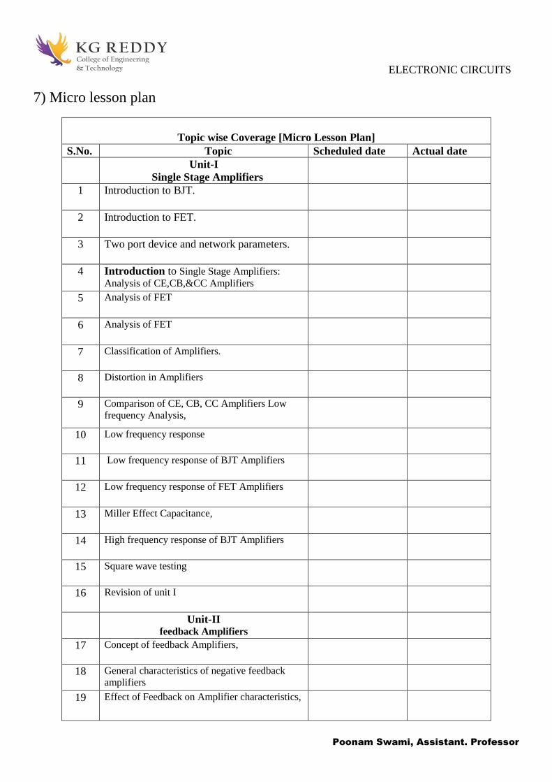
7) Micro lesson plan
Topic wise Coverage [Micro Lesson Plan]
S.No. Topic Scheduled date Actual date
Unit-I
Single Stage Amplifiers
1 Introduction to BJT.
2 Introduction to FET.
3 Two port device and network parameters.
4 Introduction to Single Stage Amplifiers:
Analysis of CE,CB,&CC Amplifiers
5 Analysis of FET
6 Analysis of FET
7 Classification of Amplifiers.
8 Distortion in Amplifiers
9 Comparison of CE, CB, CC Amplifiers Low
frequency Analysis,
10 Low frequency response
11 Low frequency response of BJT Amplifiers
12 Low frequency response of FET Amplifiers
13 Miller Effect Capacitance,
14 High frequency response of BJT Amplifiers
15 Square wave testing
16 Revision of unit I
Unit-II feedback Amplifiers
17 Concept of feedback Amplifiers,
18 General characteristics of negative feedback
amplifiers
19 Effect of Feedback on Amplifier characteristics,

ELECTRONIC CIRCUITS
Poonam Swami, Assistant. Professor
20 Voltage series, voltage shunt feedback
configurations
21 Current series and current shunt Feedback
configurations
22 Illustrative problems
23 Oscillators: Conditions for oscillations,
24 Frequency and Amplitude Stability of
Oscillators,
25 Generalized analysis of LC Oscillators
26 Quartz oscillator
27 Hartley oscillator
28 Colpitt’s oscillator
29 RC –phase shift oscillator
30 Wein Bridge oscillators
31 Revision of unit II
Unit-III Large Signal Amplifiers:
32 Class A Power Amplifier,
33 Maximum Efficiency of Class –A amplifier
34 Transformer Coupled Amplifier,
35 Push Pull Amplifier complimentary Symmetry
Class-B Power Amplifier,
36 Phase Inverters,
37 Transistor Power Dissipation,
38 Thermal Runway, Heat sinks
39 CLASS C amplifier
40 Revision of unit III
Unit-IV Wave Shaping:

ELECTRONIC CIRCUITS
Poonam Swami, Assistant. Professor
41 High Pass RC Circuits their response for
Sinusoidal, Step, Pulse and Ramp Inputs.
42 Low Pass RC Circuits their response for
Sinusoidal, Step, Pulse and Ramp Inputs.
43 Clippers and Clampers: Diode Clippers,
Transistor Clippers,
44 Clipping at Two Independent levels
45 Transfer Characteristics of Clippers,
46 Comparators, Clamping Operation,
47 Clamping Circuits using Diode with different
inputs,
48 Clamping Circuit Theorem
49 Practical Clamping Circuit
50 Revision of unit IV
Unit-V Switching Characteristics of Devices
51 Diode as a Switch,
52 Piecewise Linear Diode Characteristics
53 Transistor as a Switch,
54 Breakdown Voltage Consideration of
Transistor,
55 Design of Transistor Switch,
56 Transistor Switching Times.
57 Multi vibrators: Analysis and Design of Bi
stable multi vibrator
58 Mono stable Multi vibrators
59 A stable Multi vibrator
60 Schmitt Trigger using Transistors
61 Revision of unit V
62 Revision of all units

ELECTRONIC CIRCUITS
Poonam Swami, Assistant. Professor
8. Teaching Schedule
Subject ELECTRONIC CIRCUITS
Text Books (to be purchased by the Students)
Book 1 “Robert L Boylestead and Louis Nashelsky”,Electronic Devices and Circuit
Theory”pearson,Tenth Edition 2009
Book 2 ‘S.Salivahanan,N.Suresh kumar and vallava Raj”,Electronic Devices and
Circuits”,TMH,2nd Edition 2008
Reference Books
Book 3 Suryaprakash Rao Mothiki
Book 4 “Anil.K .Maini, Varsha Agarwal”, Electronic devices and circuits”,Wiley,1st edition
2009.
Unit
Topic Chapters Nos No of
classes Book 1 Book 2 Book 3 Book 4
I
Introduction to single stage amplifiers 1 1 1 2 1
Distorsion in amplifiers 1 2 1 1
Low frequency response of BJT and
FET amplifiers 1 1 2 3
II
Concept of feedback amplifiers 2 1 1 3 1
Types of negative feedback
amplifiers 2 1 1 3 4
oscillators 5 3 3 5
III
classA, classB Power amplifiers 7 6 4 5
Pushpull amplifiers 7 6 4 2
Phase inverters and heat sinks 7 6 4 2
IV
HighPass and LowPass RC circuits
and their response 8 7 6 5
Diode and Transistor clippers at to
independent levels 8 7 6 4
Comparators and clamping circuit
theorem 8 7 6 4
V
Practical clamping circuits 8 7 6 4
Switching characteristics of devices 9 10 9 4
Multivibrators 9 10 9 6
Contact classes for syllabus coverage 56
Lectures beyond the syllabus and gaps in syllabus 06
Total No. of classes 62

ELECTRONIC CIRCUITS
Poonam Swami, Assistant. Professor

ELECTRONIC CIRCUITS
Poonam Swami, Assistant. Professor

ELECTRONIC CIRCUITS
Poonam Swami, Assistant. Professor

ELECTRONIC CIRCUITS
Poonam Swami, Assistant. Professor

ELECTRONIC CIRCUITS
Poonam Swami, Assistant. Professor

ELECTRONIC CIRCUITS
Poonam Swami, Assistant. Professor

ELECTRONIC CIRCUITS
Poonam Swami, Assistant. Professor

ELECTRONIC CIRCUITS
Poonam Swami, Assistant. Professor

ELECTRONIC CIRCUITS
Poonam Swami, Assistant. Professor
12) Mid EXAM Descriptive Question paper Mid1

ELECTRONIC CIRCUITS
Poonam Swami, Assistant. Professor
SUBJECT CODE:EE305ES SET NO. A
KG REDDY COLLEGE OF ENGINEERING & TECHNOLOGY
Chilkur (Vill) Moinabad (Mdl) R RDist B.TECH II Year I SEM I MID Term Examinations, SEP-2018
ELECTRONIC CIRCUITS
OBJECTIVE EXAM
NAME_____________________________HALL TICKETNO
Answer all the questions. All questions carry equal marks. Time: 20min. 10 marks.
I choose correct alternative:
1. A single stage transistor amplifier contains ……………. and associated circuitry [ ]
A.Two transistors B. One transistors C. Three transistors D.None of the above
2. The purpose of capacitors in a transistor amplifier is to ……………… [ ]
A. Protect the
transistor
B. Cool the transistor
C. Couple or bypass a.c.
component
D. Provide biasing
3. For highest power gain, one would use …………….. configuration [ ]
A. CC B. CB C. CE D. none of the above
4. When negative voltage feedback is applied to an amplifier, its voltage gain
……………….
[ ]
A. Is increased B.Is reduced C.Remains the same DNone of the above
5. The gain of an amplifier with feedback is known as ………….. gain [ ]
A. Resonant B. Open loop C. Closed loop D. None of the above
6. An oscillator converts …………….. [ ]
A. ac. power into
d.c. power
B. dc. power into a.c.
power
C. mechanical power into
a.c. power
D. none of the above
7. In a phase shift oscillator, the frequency determining elements are ………… [ ]
A. L and C B. R, L and C C. R and C D. None of the above
8. The maximum efficiency of resistance loaded class A power amplifier is …….. [ ]
A. 5% B. 50% C. 30% D. 25%
Q M A

ELECTRONIC CIRCUITS
Poonam Swami, Assistant. Professor
9. In class A operation, the operating point is generally located ………. of the d.c.
load line.
[ ]
A. At cut off point B. At the middle C. At saturation point D. None of the above
10. The maximum efficiency of transformer coupled class A power amplifier is
………………
[ ]
A. 30%
B. 50%
C. 80%
D. 45%
Count…..2
SUBJECT CODE: EE305ES SET NO. A
II Fill in the Blanks:
1. The main advantage of multi stage amplifiers is _______
2. Cascode amplifier is a combination of ________
3. The decibel gain of a cascaded system is the ________ of the decibel gains of each stage.
4. The ________ region produces the maximum voltage gain in a single-stage BJT or FET
amplifier.
5. The Trans conductance amplifier is also called as ______________
6. The oscillator which uses inductive feedback is ________
7. In a RC phase shift oscillator, each RC section provides a phase shift of _________
8. In ________ power amplifiers, the output signal varies for a full 360º of the cycle.
9. For proper amplification, by the transistor circuits the operating point should be located at
__________ of the dc load line.
10. ____________ Coupling is generally used in power amplifiers.

ELECTRONIC CIRCUITS
Poonam Swami, Assistant. Professor
Code No: 126ZN Set No. 1 Electronics circuits
KEY I choose the correct alternative: 1) One transistor
2) Couple or bypass AC component
3) CE
4) Reduced
5) Closed loop
6) dc power to ac power
7) R & C
8) 25%
9) At the middle
10) 50%
Fill in the blanks:
1) High gain
2) CE-CB
3) Sum
4) Mid frequency
5) Current series amplifier (series series)
6) Hartley
7) 60°
8) Class A
9) The middle
10) Transformer

ELECTRONIC CIRCUITS
Poonam Swami, Assistant. Professor
14) Assignment Topics Unit wise
Unit1: Single Stage Amplifiers
1. Classification of amplifiers.
2 Comparison of CE, CC, CB amplifiers.
ELECTRONIC CIRCUITS
Poonam Swami, Assistant. Professor
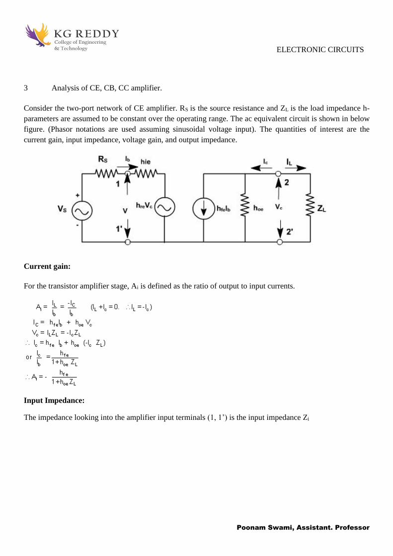
3 Analysis of CE, CB, CC amplifier.
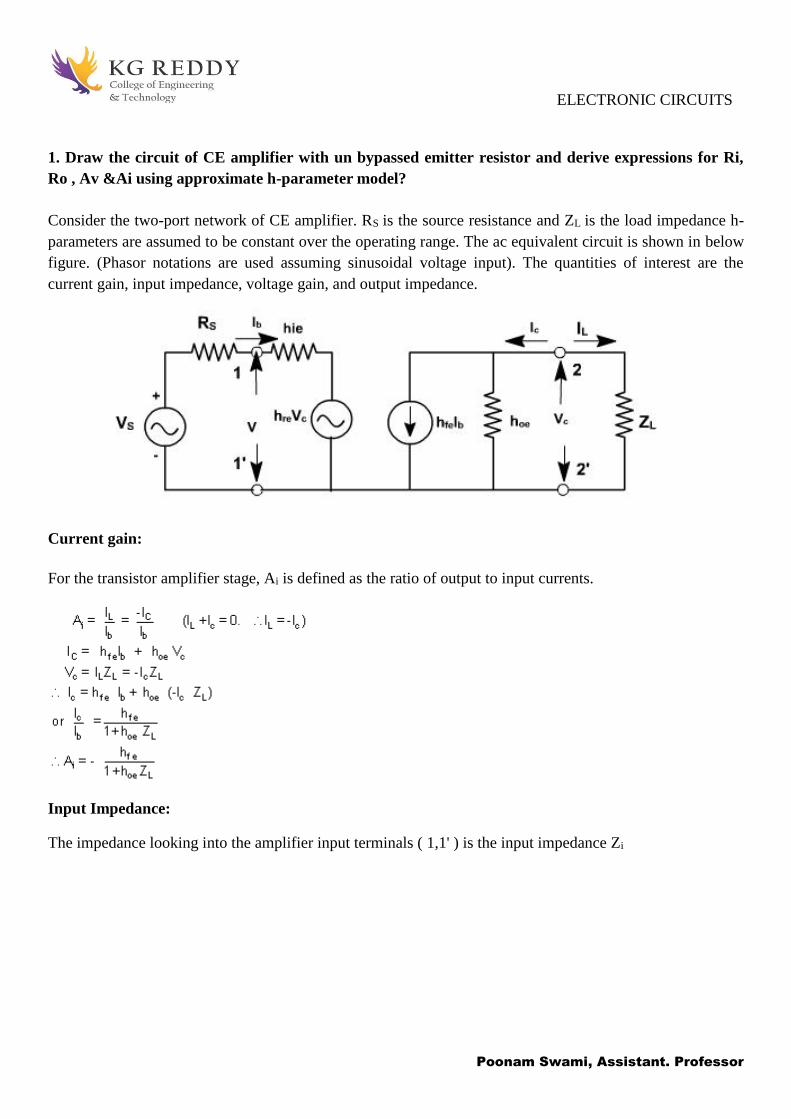
Consider the two-port network of CE amplifier. RS is the source resistance and ZL is the load impedance h-
parameters are assumed to be constant over the operating range. The ac equivalent circuit is shown in below
figure. (Phasor notations are used assuming sinusoidal voltage input). The quantities of interest are the
current gain, input impedance, voltage gain, and output impedance.
Current gain:
For the transistor amplifier stage, Ai is defined as the ratio of output to input currents.
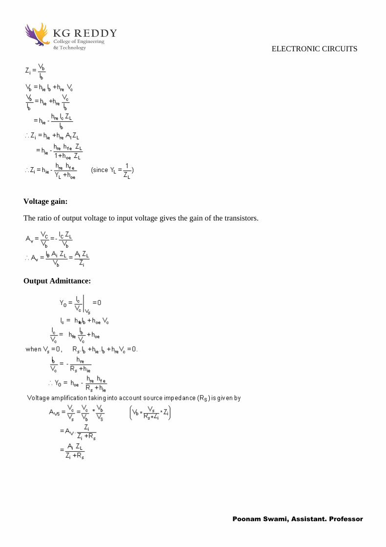
Input Impedance:
The impedance looking into the amplifier input terminals (1, 1’) is the input impedance Zi
ELECTRONIC CIRCUITS
Poonam Swami, Assistant. Professor
Voltage gain:
The ratio of output voltage to input voltage gives the gain of the transistors.
Output Admittance:

ELECTRONIC CIRCUITS
Poonam Swami, Assistant. Professor
4 Low frequency analysis of BJT
In a low frequency region of the single stage BJT amplifier, it is the RC combinations formed by the
capacitors Cin,CE,Cout, Cin,CE,Cout -Electronic Devices and Circuit Theory-Boylestad
Considering the equivalent circuit formed as shown in fig.1
The output voltage and input voltage are related by:
Vout=RR−jXCVinVout=RR−jXCVin

ELECTRONIC CIRCUITS
Poonam Swami, Assistant. Professor
The magnitude is given by
Vout=R[R2+X2C]1/2VinVout=R[R2+XC2]1/2Vin
When XC=RWhen XC=R
Vout=0.707VinVout=0.707Vin
The frequency at which this occur, is given by the equation,
R=XC=12πfLCR=XC=12πfLC
or, 3dB cutoff frequency
fL=12πRCfL=12πRC
In case the equivalent circuit formed by the BJT circuit is something like fig 2, which is the case when we
are considering the input portion of the BJT circuit, the analysis is something like this:
Vin=RinRin+RS−jXCVinVin=RinRin+RS−jXCVin
The magnitude is given by
Vin=Rin[(Rin+RS)2+X2C]1/2VinVin=Rin[(Rin+RS)2+XC2]1/2Vin
When XC=RS+RinWhen XC=RS+Rin
=>12πfCin=Rin+RS=>12πfCin=Rin+RS
=>f=12π(Rin+RS)Cin=>f=12π(Rin+RS)Cin
But for XC=RS+RinXC=RS+Rin
Vin=0.707Rin(RS+Rin)VSVin=0.707Rin(RS+Rin)VS
Which is not
Vin=0.707VSVin=0.707VS
How is then the cutoff frequency equal to 12π(RS+Rin)Cin12π(RS+Rin)Cin in case of Figure 2 ?
Furthur,
For
Vin=0.707VSVin=0.707VS
Rin[(Rin+RS)2+X2C]1/2Vin=121/2Rin[(Rin+RS)2+XC2]1/2Vin=121/2
=>Rin(Rin+RS)2+X2C=12=>Rin(Rin+RS)2+XC2=12
=>2R2in=(Rin+RS)2+X2C=>2Rin2=(Rin+RS)2+XC2
=>X2C=(Rin−RS)2=>XC2=(Rin−RS)2
=>Xc=Rin−RS

ELECTRONIC CIRCUITS
Poonam Swami, Assistant. Professor
5 Low frequency analysis of FET
Low frequency analysis of FET amplifier:
From above figure, it has two RC networks that affect its gain as the frequency is reduced below midrange.
These are,
1. RC network formed by the input coupling capacitor C1 and input impedance of the amplifier.
2. RC network formed by the output coupling capacitor and the output impedance looking in at the drain.
`Input RC network:
Lower critical frequency of this network is given as,
The value of Rin(gate) can be determined from the data sheet as follows:

ELECTRONIC CIRCUITS
Poonam Swami, Assistant. Professor
The phase shift in low frequency input RC circuit is θ = tan-1 (XC1 / Rin )
Output RC network:
Lower critical frequency of this network is given as,
The phase shift in low frequency output RC circuit is θ = tan-1 (XC2 / RD + RL)
Unit2: Feedback Amplifiers and oscillators.
1) Define the concept of feedback in amplifiers?
Feedback is defined as the process in which a part of output signal (voltage or current) is returned back
to the input. The amplifier that operates on the principle of feedback is known as feedback amplifier.
2) Write the advantages of negative feedback?
ADVANTAGES
Input resistance increases
Output resistance decreases
Bandwidth increases
Non linear distortion decreases
Frequency distortion decreases
Sensitivity will be decreased
Gain stability
DISADVANTAGES
Decrease in gain
3) Explain condition for oscillation.
The use of positive feedback is useful for producing oscillators. The condition for positive feedback is that a
portion of the output is combined in phase with the input. For an amplifer with positive feedback the gain is
given by the expression below
ELECTRONIC CIRCUITS
Poonam Swami, Assistant. Professor
The large open loop gain of an op-amp makes it inevitable that the condition
And the gain expression
Becomes infinite
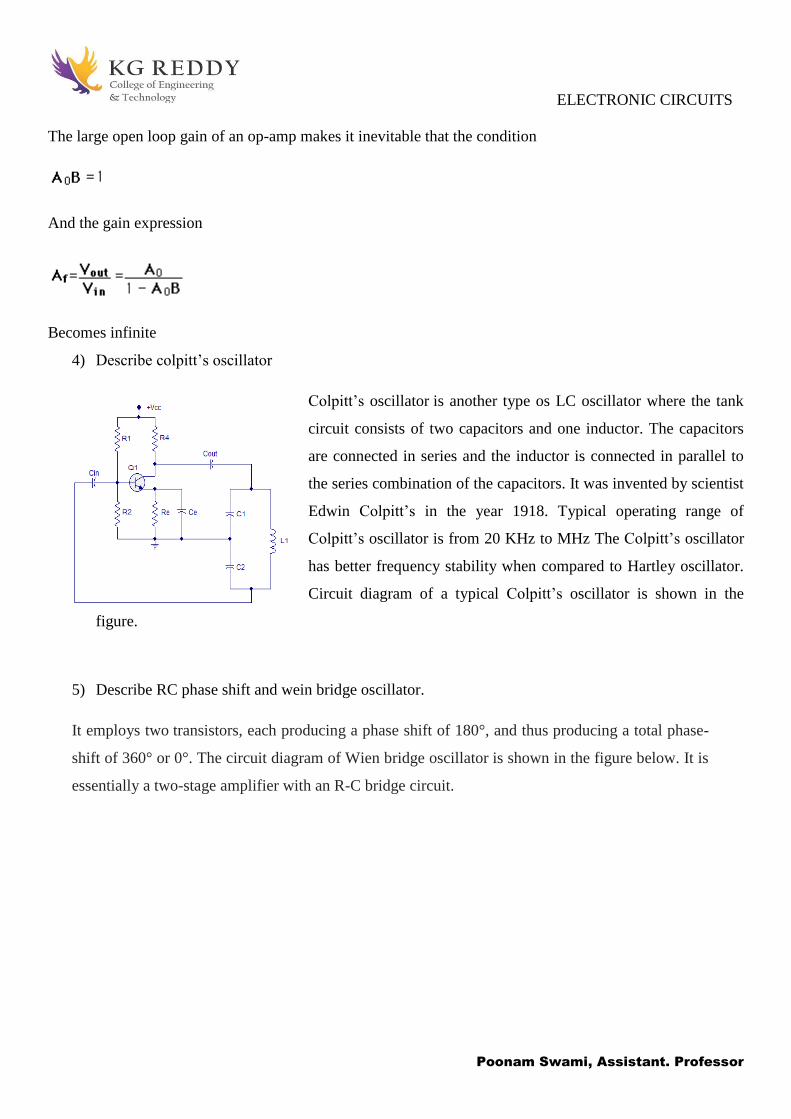
4) Describe colpitt’s oscillator
Colpitt’s oscillator is another type os LC oscillator where the tank
circuit consists of two capacitors and one inductor. The capacitors
are connected in series and the inductor is connected in parallel to
the series combination of the capacitors. It was invented by scientist
Edwin Colpitt’s in the year 1918. Typical operating range of
Colpitt’s oscillator is from 20 KHz to MHz The Colpitt’s oscillator
has better frequency stability when compared to Hartley oscillator.
Circuit diagram of a typical Colpitt’s oscillator is shown in the
figure.
5) Describe RC phase shift and wein bridge oscillator.
It employs two transistors, each producing a phase shift of 180°, and thus producing a total phase-
shift of 360° or 0°. The circuit diagram of Wien bridge oscillator is shown in the figure below. It is
essentially a two-stage amplifier with an R-C bridge circuit.

ELECTRONIC CIRCUITS
Poonam Swami, Assistant. Professor

ELECTRONIC CIRCUITS
Poonam Swami, Assistant. Professor
Unit3: large Signal Amplifiers
1) Explain class A power amplifier
Class A amplifier: In class-A amplifiers the collector is biased at a value greater than the amplitude of
AC signal current. Hence the conduction angle is 360 Degrees i.e. the Class A stage conducts for the
entire cycle for the input signal.

ELECTRONIC CIRCUITS
Poonam Swami, Assistant. Professor
2) Calculate maximum effiency for class A power amplifier.
As shown in circuit diagram below, a load is connected in the collector circuit either directly or through
a coupling transformer. Usually, the load is connected through an output transformer because it provides
the perfect impedance matching due to which maximum power can be transferred to the load and keeps the
DC power loss small because of small resistance of the transformer primary winding.
As we know, at zero signal conditions the effective resistance in the collector circuit is almost zero, since the
primary winding resistance of the transformer is very small & can be neglected. As shown in its waveform, a
line passing through the Vcc & parallel to the axis of collector current IC is known as DC load line. Draw the
AC load line by cutting the DC load line at Q (operating point) such that Q lies at the centre of AC load line.
Calculation of Collector Efficiency:
To obtain maximum AC power output and hence maximum collector efficiency, the peak value of collector
current due to signal alone should be equal to zero signal collector current.
When positive half cycle is at its peak:
Total collector current =2 Ic
And,
Vce = 0
When negative half cycle is at its peak:
Total collector current =0
and,
Vce = 2 Vcc
Therefore, Peak to peak emitter voltage is given as,

ELECTRONIC CIRCUITS
Poonam Swami, Assistant. Professor
Vce (peak to peak) = 2 Vcc
Peak to peak collector current is given as,
Ic (peak to peak) = 2 Ic
= Vce (peak to peak) / RL
= 2 Vcc / RL’
where,
RL’ = Effective value of load resistance RL when referred to primary side.
i.e.
RL’ = n2 RL
As we know, DC power input and AC power output is given as,
Pdc = Vcc Ic = Ic2 RL’
Pac = [Vce (peak to peak) * Ic (peak to peak) ] / 8
= (2 Vcc * 2 Ic ) / 8
= 1/ 2 Vcc Ic
= 1/ 2 Ic2 RL’
Therefore, maximum collector efficiency is given by,
η max = (Pac / Pdc ) * 100
Substitute the value of DC power input and AC power output in the above equation, we get,
η max = [(Ic2 RL’) / 2 Ic
2 RL’ ] * 100
η max = 50%
The above expression shows that in class A amplifier, maximum 50% of the DC power supplied can be
converted into AC power output. Due to power loss in the primary of the transformer, the
collector efficiency of class A amplifier is always less than 50%. It may be noted that maximum power is
dissipated in the transistor in the zero signal condition i.e. given as,
Pdis = Vcc Ic
Note: Before selecting a transistor always remember that its power rating be >= Pdis.

ELECTRONIC CIRCUITS
Poonam Swami, Assistant. Professor
Advantages and Disadvantages of Class A power amplifier:
In the electronics industry, we use power amplifiers for various purposes depending upon the requirement.
Each and every amplifier has its own pros and cons as per its reliability and efficiency.
Advantages of Class A amplifier:
Following of its merits are:
It has high fidelity because at output exact replica of an input signal is produced.
Its Designing is simple.
It has improved high-frequency response because the active device is On full time i.e no time is
required for turn on the device.
There is no crossover distortion because the active device conducts for the entire cycle of the input
signal.
Single ended configuration can be easily & practically realized in class A amp.
Disadvantages of Class A amplifier:
Following of its demerits are:
Due to the large power supply and heat sink, class A amp are costly and bulky.
It has Poor Efficiency.
Due to transformer coupling frequency response is not good.
3) Explain class B power amplifier
Class B Amplifier Operation
Unlike the Class A amplifier mode of operation above that uses a single transistor for its output power stage,
the Class B Amplifier uses two complimentary transistors (either an NPN and a PNP or a NMOS and a
PMOS) for each half of the output waveform. One transistor conducts for one-half of the signal waveform
while the other conducts for the other or opposite half of the signal waveform. This means that each
transistor spends half of its time in the active region and half its time in the cut-off region thereby
amplifying only 50% of the input signal.
Class B operation has no direct DC bias voltage like the class A amplifier, but instead the transistor only
conducts when the input signal is greater than the base-emitter voltage and for silicon devices is about 0.7v.
Therefore, at zero input there is zero output. This then results in only half the input signal being presented at
the amplifiers output giving a greater amount of amplifier efficiency as shown below.

ELECTRONIC CIRCUITS
Poonam Swami, Assistant. Professor
Class B Output Waveform
In a class B amplifier, no DC voltage is used to bias the transistors, so for the output transistors to start to
conduct each half of the waveform, both positive and negative, they need the base-emitter voltage Vbe to be
greater than the 0.7v required for a bipolar transistor to start conducting.
Then the lower part of the output waveform which is below this 0.7v window will not be reproduced
accurately resulting in a distorted area of the output waveform as one transistor turns “OFF” waiting for the
other to turn back “ON”. The result is that there is a small part of the output waveform at the zero voltage
cross over point which will be distorted. This type of distortion is called Crossover Distortion
4) What is thermal runway and why heat sink is used.
TRANSISTOR POWER DISSIPATION
There is not a clear cut difference between ‘ordinary’ transistors used in voltage amplifiers
and power transistors, but generally Power transistors can be categorised as those than can handle
more than 1 Ampere of collector (or Drain in the case of FETs) current.
power transistors can handle larger currents and higher voltages.
they have a different construction to small signal devices.
They must have low output resistances so that they can deliver large currents to the load, a good
junction insulation to withstand high voltages.
They must also be able to dissipate heat very quickly so they do not overheat.
As most heat is generated at the collector/base junction, the area of this junction is made

ELECTRONIC CIRCUITS
Poonam Swami, Assistant. Professor
HEAT SINKS
A heat-sink is designed to remove heat from a transistor
and dissipate it into the surrounding air as efficiently as
possible. Heat-sinks take many different forms, such as
finned aluminum or copper sheets or blocks, often painted
or anodized matt black to help dissipate heat more
quickly. A selection of heat-sinks is illustrated in Figure.
Good physical contact between the transistor and heat-
sink is essential, and a heat transmitting grease (heat-sink
compound) is smeared on the contact area before
clamping the transistor to the heat-sink.
Where it is necessary to maintain electrical insulation between transistor and heat-sink a mica layer is used
between the heat-sink and transistor. Mica has excellent insulation and very good heat conducting properties
Heat Sink Types
Active Heat Sinks. These are generally fan type and utilize power for cooling purpose. They can also
be termed as Heat sink or fans. ...
Passive Heat Sinks. ...
Aluminum Heat Sink. ...
Stamped Heat Sinks. ...
Machining Heat Sinks. ...
Bonded-Fin Heat Sinks. ...
Folded-Fin Heat Sinks. ...
Skived Heat Sinks.
as large as possible
ELECTRONIC CIRCUITS
Poonam Swami, Assistant. Professor
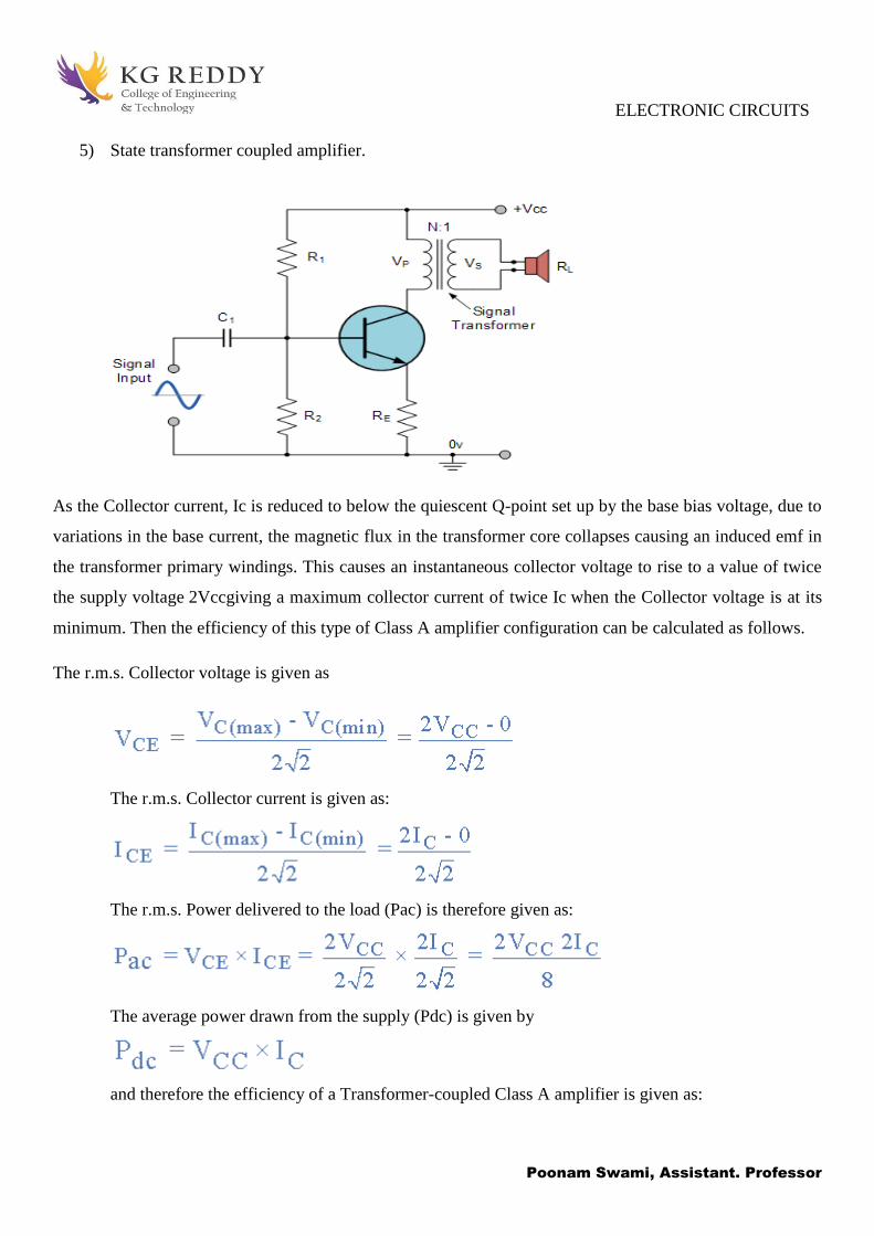
5) State transformer coupled amplifier.
As the Collector current, Ic is reduced to below the quiescent Q-point set up by the base bias voltage, due to
variations in the base current, the magnetic flux in the transformer core collapses causing an induced emf in
the transformer primary windings. This causes an instantaneous collector voltage to rise to a value of twice
the supply voltage 2Vccgiving a maximum collector current of twice Ic when the Collector voltage is at its
minimum. Then the efficiency of this type of Class A amplifier configuration can be calculated as follows.
The r.m.s. Collector voltage is given as
The r.m.s. Collector current is given as:
The r.m.s. Power delivered to the load (Pac) is therefore given as:
The average power drawn from the supply (Pdc) is given by
and therefore the efficiency of a Transformer-coupled Class A amplifier is given as:
ELECTRONIC CIRCUITS
Poonam Swami, Assistant. Professor
Unit4: Wave shaping and Clippers and clampers.
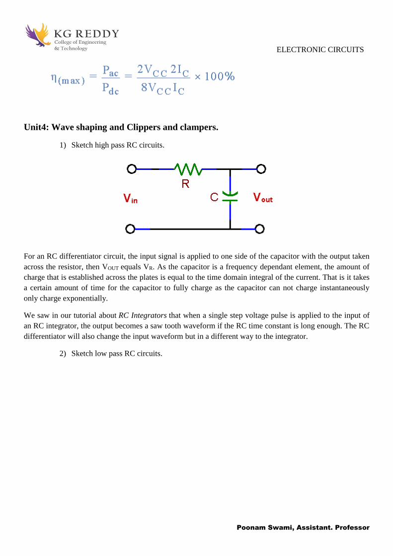
1) Sketch high pass RC circuits.
For an RC differentiator circuit, the input signal is applied to one side of the capacitor with the output taken
across the resistor, then VOUT equals VR. As the capacitor is a frequency dependant element, the amount of
charge that is established across the plates is equal to the time domain integral of the current. That is it takes
a certain amount of time for the capacitor to fully charge as the capacitor can not charge instantaneously
only charge exponentially.
We saw in our tutorial about RC Integrators that when a single step voltage pulse is applied to the input of
an RC integrator, the output becomes a saw tooth waveform if the RC time constant is long enough. The RC
differentiator will also change the input waveform but in a different way to the integrator.
2) Sketch low pass RC circuits.

ELECTRONIC CIRCUITS
Poonam Swami, Assistant. Professor

ELECTRONIC CIRCUITS
Poonam Swami, Assistant. Professor
3) Explain clippers
An electronic circuit that is used to alter the positive peak or negative peak of the input signal to a definite
value by shifting the entire signal up or down to obtain the output signal peaks at desired level is called as
Clamper circuit.
Working of Clipper Circuit
The clipper circuit can be designed by utilizing both the linear and nonlinear elements such as resistors,
diodes or transistors. As these circuits are used only for clipping input waveform as per the requirement and
for transmitting the waveform, they do not contain any energy storing element like a capacitor.
In general, clippers are classified into two types: Series Clippers and Shunt Clippers.
4) Explain clampers.
The positive or negative peak of a signal can be positioned at the desired level by using the clamping
circuits. As we can shift the levels of peaks of the signal by using a clamper, hence, it is also called as level
shifter.
The clamper circuit consists of a capacitor and diode connected in parallel across the load. The clamper
circuit depends on the change in the time constant of the capacitor. The capacitor must be chosen such that,
during the conduction of the diode, the capacitor must be sufficient to charge quickly and during the non
conducting period of diode, the capacitor should not discharge drastically. The clampers are classified as
positive and negative clampers based on the clamping method.
5) working principal of simple diode comparator
An operational amplifier (op-amp) has a well balanced difference input and a very high gain. This parallels
the characteristics of comparators and can be substituted in applications with low-performance
requirements.[4]
In theory, a standard op-amp operating in open-loop configuration (without negative feedback) may be used
as a low-performance comparator. When the non-inverting input (V+) is at a higher voltage than the
inverting input (V-), the high gain of the op-amp causes the output to saturate at the highest positive voltage
it can output. When the non-inverting input (V+) drops below the inverting input (V-), the output saturates at
the most negative voltage it can output. The op-amp's output voltage is limited by the supply voltage. An op-
amp operating in a linear mode with negative feedback, using a balanced, split-voltage power supply,

ELECTRONIC CIRCUITS
Poonam Swami, Assistant. Professor
(powered by ± VS) has its transfer function typically written as: . However, this equation may not be
applicable to a comparator circuit which is non-linear and operates open-loop (no negative feedback)
In practice, using an operational amplifier as a comparator presents several disadvantages as compared to
using a dedicated comparator:[5]
1. Op-amps are designed to operate in the linear mode with negative feedback. Hence, an op-amp
typically has a lengthy recovery time from saturation. Almost all op-amps have an internal
compensation capacitor which imposes slew rate limitations for high frequency signals.
Consequently, an op-amp makes a sloppy comparator with propagation delays that can be as long as
tens of microseconds.
2. Since op-amps do not have any internal hysteresis, an external hysteresis network is always
necessary for slow moving input signals.
3. The quiescent current specification of an op-amp is valid only when the feedback is active. Some op-
amps show an increased quiescent current when the inputs are not equal.
4. A comparator is designed to produce well limited output voltages that easily interface with digital
logic. Compatibility with digital logic must be verified while using an op-amp as a comparator.
5. Some multiple-section op-amps may exhibit extreme channel-channel interaction when used as
comparators.
6. Many op-amps have back to back diodes between their inputs. Op-amp inputs usually follow each
other so this is fine. But comparator inputs are not usually the same. The diodes can cause
unexpected current through inputs.
Unit5: Switching characteristics of devices and multivibrators.
1) Explain diode as a switch
In addition to their use as simple rectifiers, diodes are also used in circuits that mix signals together
(mixers), detect the presence of a signal (detector), and act as a switch “to open or close a circuit”. Diodes
used in these applications are commonly referred to as “signal diodes”. The simplest application of a signal
diode is the basic diode switch shown in figure 1.
When the input to this circuit is at zero potential, the diode is forward biased because of the zero potential
on the cathode and the positive voltage on the anode. In this condition, the diode conducts and acts as a
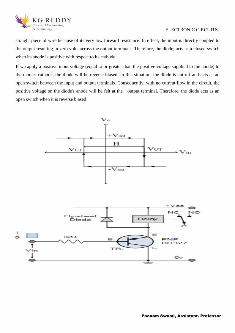
ELECTRONIC CIRCUITS
Poonam Swami, Assistant. Professor
straight piece of wire because of its very low forward resistance. In effect, the input is directly coupled to
the output resulting in zero volts across the output terminals. Therefore, the diode, acts as a closed switch
when its anode is positive with respect to its cathode.
If we apply a positive input voltage (equal to or greater than the positive voltage supplied to the anode) to
the diode's cathode, the diode will be reverse biased. In this situation, the diode is cut off and acts as an
open switch between the input and output terminals. Consequently, with no current flow in the circuit, the
positive voltage on the diode's anode will be felt at the output terminal. Therefore, the diode acts as an
open switch when it is reverse biased

ELECTRONIC CIRCUITS
Poonam Swami, Assistant. Professor
2) Explain transistor as a switch
Transistor act as a switch- Working and transistor switching circuit
Consider the first figure in which base terminal of the npn transistor is closed then the transistor is said to be
in ON state (similar to a short circuit between Vcc and Ground) so the collector voltage is very low (0.02V
approx).Whole current from Vcc will flows through the transistor, no current flow through the LED because
current chooses low resistance path. Therefore LED connected at the Collector is in OFF state since the
voltage at the anode of LED is 0.02V. Consider the second figure, when the voltage at the base terminal
removed (open circuit), the transistor become OFF (means an open circuit between Vcc and Ground) then its
collector voltage will be Vcc (Supply voltage) Since the transistor is in OFF state, the whole current will
flows trough the LED, Then the LED glows.
Transistor is a semiconductor device used for switching and amplification of weak signals. This article
explains how a transistor work and the working of transistor as a switch. At present, transistors are applied
in most of the electronic equipments for switching purposes. Digital ICs, Microcontrollers, etc uses
thousands of embedded transistors for switching. The huge electrical networks are also switched by simple
transistor switching circuit (Most of the Power electronics circuits). Here we are discussing about NPN
transistor switching circuit. To realize the exact working principle, an LED (Light Emitting Diode) is
connected to the collector of NPN transistor. It glows according to the base current. Don’t forget to connect
the base resistor (Rb) to limit the base current other wise the transistor become damage. Transistor switching
circuits are also employed in DC Motor driver circuit.
3) What are the applications of Schmitt trigger circuit?
1. The Schmitt trigger is a comparator application which switches the output negative when the input
passes upward through a positive reference voltage.
2. It then uses positive feedback of a negative voltage to prevent switching back to the
other state until the input passes through a lower threshold voltage, thus stabilizing the switching
against rapid triggering by noise as it passes the trigger point.

ELECTRONIC CIRCUITS
Poonam Swami, Assistant. Professor
3. That is, it provides feedback which is not reversed in phase, but in this case the signal that is being
fed back is a negative signal and keeps the output driven to the negative supply voltage until the
input drops below the lower design threshold.
4) .Why the mono stable circuit is also called as delay circuit?
Multi vibrators have two different electrical states, an output “HIGH” state and an output “LOW” state
giving them either a stable or quasi-stable state depending upon the type of multi vibrator. One such type of
a two state pulse generator configuration is called Mono stable Multi vibrators.
Mono stable Multi vibrators or “One-Shot Multi vibrators” as they are also called, are used to generate a
single output pulse of a specified width, either “HIGH” or “LOW” when a suitable external trigger signal or
pulse T is applied. This trigger signal initiates a timing cycle which causes the output of the mono stable to
change its state at the start of the timing cycle and will remain in this second state.
5) Explain the operation of mono stable multi vibrator with waveforms.
Monostable multivibrator has one stable state and one quasi stable state (astable state). When an external
trigger applied to the circuit, the multivibrator will jump to quasi stable state from stable state. After the
period of time it will automatically set back to the stable state, for returning to the stable state multivibrator
does not require any external trigger. The time period to returning to stable state circuit is always depends on
the passive elements in the circuit (resistor and capacitor values
ELECTRONIC CIRCUITS
Poonam Swami, Assistant. Professor
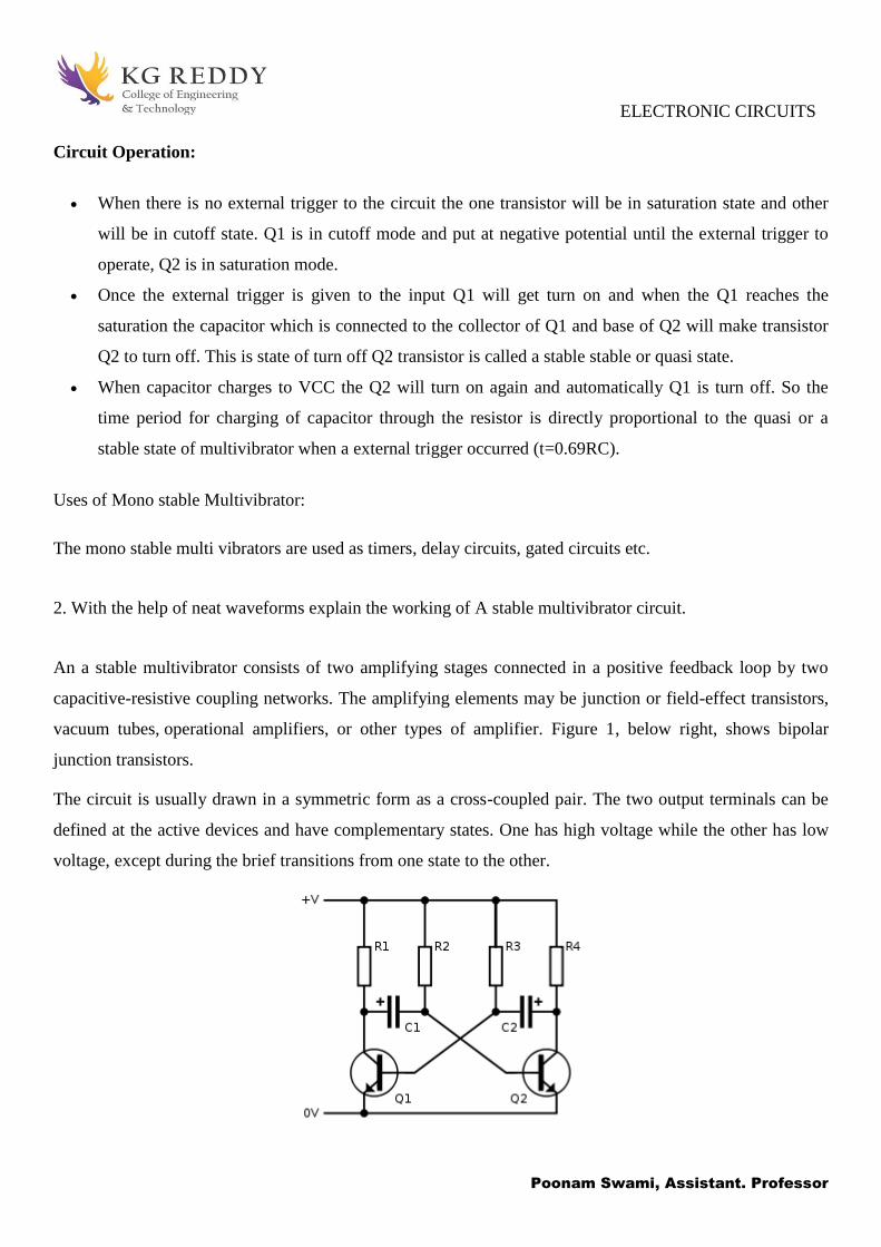
Circuit Operation:
When there is no external trigger to the circuit the one transistor will be in saturation state and other
will be in cutoff state. Q1 is in cutoff mode and put at negative potential until the external trigger to
operate, Q2 is in saturation mode.
Once the external trigger is given to the input Q1 will get turn on and when the Q1 reaches the
saturation the capacitor which is connected to the collector of Q1 and base of Q2 will make transistor
Q2 to turn off. This is state of turn off Q2 transistor is called a stable stable or quasi state.
When capacitor charges to VCC the Q2 will turn on again and automatically Q1 is turn off. So the
time period for charging of capacitor through the resistor is directly proportional to the quasi or a
stable state of multivibrator when a external trigger occurred (t=0.69RC).
Uses of Mono stable Multivibrator:
The mono stable multi vibrators are used as timers, delay circuits, gated circuits etc.
2. With the help of neat waveforms explain the working of A stable multivibrator circuit.
An a stable multivibrator consists of two amplifying stages connected in a positive feedback loop by two
capacitive-resistive coupling networks. The amplifying elements may be junction or field-effect transistors,
vacuum tubes, operational amplifiers, or other types of amplifier. Figure 1, below right, shows bipolar
junction transistors.
The circuit is usually drawn in a symmetric form as a cross-coupled pair. The two output terminals can be
defined at the active devices and have complementary states. One has high voltage while the other has low
voltage, except during the brief transitions from one state to the other.
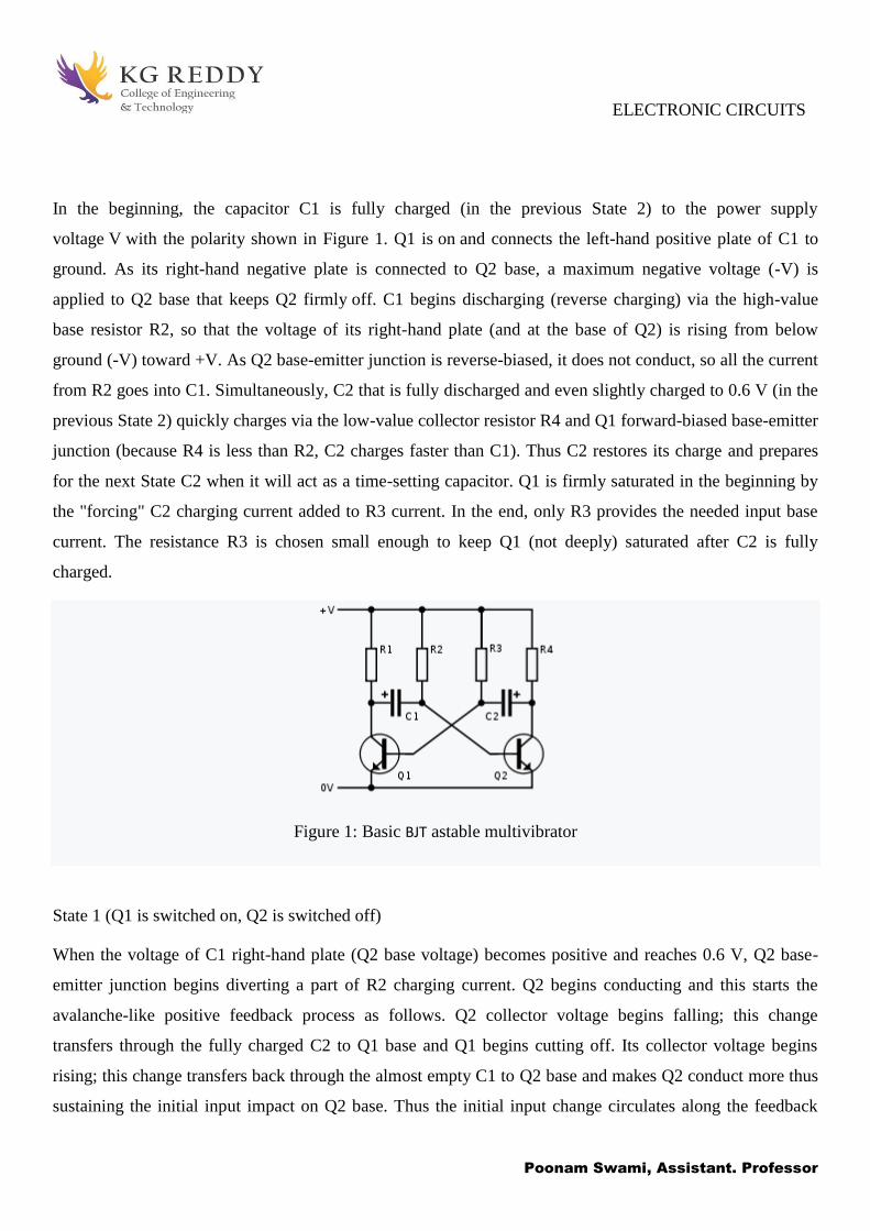
ELECTRONIC CIRCUITS
Poonam Swami, Assistant. Professor
In the beginning, the capacitor C1 is fully charged (in the previous State 2) to the power supply
voltage V with the polarity shown in Figure 1. Q1 is on and connects the left-hand positive plate of C1 to
ground. As its right-hand negative plate is connected to Q2 base, a maximum negative voltage (-V) is
applied to Q2 base that keeps Q2 firmly off. C1 begins discharging (reverse charging) via the high-value
base resistor R2, so that the voltage of its right-hand plate (and at the base of Q2) is rising from below
ground (-V) toward +V. As Q2 base-emitter junction is reverse-biased, it does not conduct, so all the current
from R2 goes into C1. Simultaneously, C2 that is fully discharged and even slightly charged to 0.6 V (in the
previous State 2) quickly charges via the low-value collector resistor R4 and Q1 forward-biased base-emitter
junction (because R4 is less than R2, C2 charges faster than C1). Thus C2 restores its charge and prepares
for the next State C2 when it will act as a time-setting capacitor. Q1 is firmly saturated in the beginning by
the "forcing" C2 charging current added to R3 current. In the end, only R3 provides the needed input base
current. The resistance R3 is chosen small enough to keep Q1 (not deeply) saturated after C2 is fully
charged.
Figure 1: Basic BJT astable multivibrator
State 1 (Q1 is switched on, Q2 is switched off)
When the voltage of C1 right-hand plate (Q2 base voltage) becomes positive and reaches 0.6 V, Q2 base-
emitter junction begins diverting a part of R2 charging current. Q2 begins conducting and this starts the
avalanche-like positive feedback process as follows. Q2 collector voltage begins falling; this change
transfers through the fully charged C2 to Q1 base and Q1 begins cutting off. Its collector voltage begins
rising; this change transfers back through the almost empty C1 to Q2 base and makes Q2 conduct more thus
sustaining the initial input impact on Q2 base. Thus the initial input change circulates along the feedback

ELECTRONIC CIRCUITS
Poonam Swami, Assistant. Professor
loop and grows in an avalanche-like manner until finally Q1 switches off and Q2 switches on. The forward-
biased Q2 base-emitter junction fixes the voltage of C1 right-hand plate at 0.6 V and does not allow it to
continue rising toward +V.
State 2 (Q1 is switched off, Q2 is switched on)
Now, the capacitor C2 is fully charged (in the previous State 1) to the power supply voltage V with the
polarity shown in Figure 1. Q2 is onand connects the right-hand positive plate of C2 to ground. As its left-
hand negative plate is connected to Q1 base, a maximum negative voltage (-V) is applied to Q1 base that
keeps Q1 firmly off. C2 begins discharging (reverse charging) via the high-value base resistor R3, so that
the voltage of its left-hand plate (and at the base of Q1) is rising from below ground (-V) toward +V.
Simultaneously, C1 that is fully discharged and even slightly charged to 0.6 V (in the previous State 1)
quickly charges via the low-value collector resistor R1 and Q2 forward-biased base-emitter junction
(because R1 is less than R3, C1 charges faster than C2). Thus C1 restores its charge and prepares for the
next State 1 when it will act again as a time-setting capacitor...and so on... (the next explanations are a
mirror copy of the second part of State 1).

ELECTRONIC CIRCUITS
Poonam Swami, Assistant. Professor
16) Unit wise Question bank:
Unit1
a) 2 marks 5 questions with answer
1. What is network and explain about two port network?
Network: A network is a collection of interconnected components. Network analysis is the process of
finding the voltages across, and the currents through, every component in the network.
Two port network:
A transistor can be treated as a two part network. The terminal
behavior of any two part network can be specified by the
terminal voltages V1 & V2 at parts 1 & 2 respectively and
current i1 and i2, entering parts 1 & 2, respectively, as shown
in figure.
2. What are the advantages of h parameter model?
Use of h – parameters to describe a transistor has the following advantages.
h – Parameters are real numbers up to radio frequencies.
They are easy to measure
They can be determined from the transistor static characteristics curves.
They are convenient to use in circuit analysis and design.
Easily convert able from one configuration to other.
Readily supplied by manufactories
3. What is the advantage of emitter resistance in CE amplifier?
The voltage gain of a CE stage depends upon hfe. This transistor
parameter depends upon temperature, aging and the operating point.
Moreover, hfe may vary widely from device to device, even for same
type of transistor. To stabilize voltage gain A V of each stage, it
should be independent of hfe. A simple and effective way is to
connect an emitter resistor Re as shown in Figure. The resistor
provides negative feedback and provides stabilization.
Figure: CE amplifier with RE
ELECTRONIC CIRCUITS
Poonam Swami, Assistant. Professor
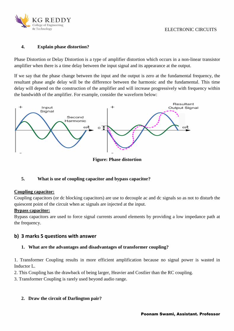
4. Explain phase distortion?
Phase Distortion or Delay Distortion is a type of amplifier distortion which occurs in a non-linear transistor
amplifier when there is a time delay between the input signal and its appearance at the output.
If we say that the phase change between the input and the output is zero at the fundamental frequency, the
resultant phase angle delay will be the difference between the harmonic and the fundamental. This time
delay will depend on the construction of the amplifier and will increase progressively with frequency within
the bandwidth of the amplifier. For example, consider the waveform below:
Figure: Phase distortion
5. What is use of coupling capacitor and bypass capacitor?
Coupling capacitor:
Coupling capacitors (or dc blocking capacitors) are use to decouple ac and dc signals so as not to disturb the
quiescent point of the circuit when ac signals are injected at the input.
Bypass capacitor:
Bypass capacitors are used to force signal currents around elements by providing a low impedance path at
the frequency.
b) 3 marks 5 questions with answer
1. What are the advantages and disadvantages of transformer coupling?
1. Transformer Coupling results in more efficient amplification because no signal power is wasted in
Inductor L.
2. This Coupling has the drawback of being larger, Heavier and Costlier than the RC coupling.
3. Transformer Coupling is rarely used beyond audio range.
2. Draw the circuit of Darlington pair?
ELECTRONIC CIRCUITS
Poonam Swami, Assistant. Professor
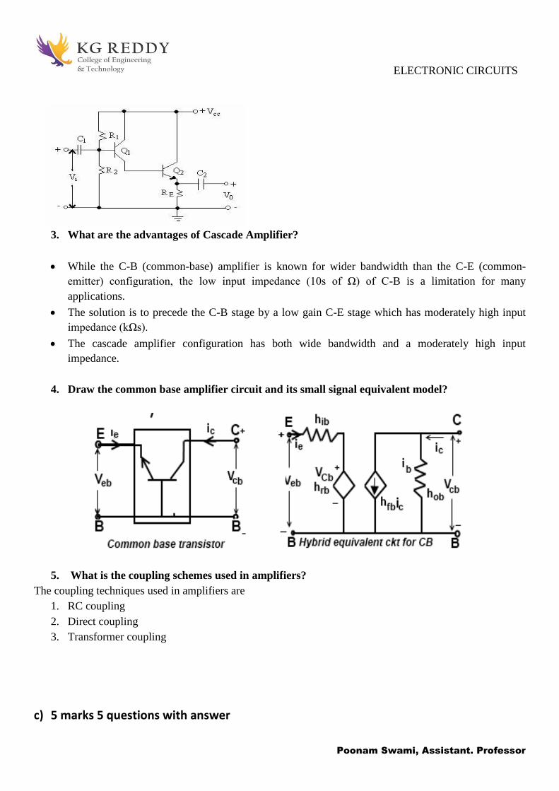
3. What are the advantages of Cascade Amplifier?
While the C-B (common-base) amplifier is known for wider bandwidth than the C-E (common-
emitter) configuration, the low input impedance (10s of Ω) of C-B is a limitation for many
applications.
The solution is to precede the C-B stage by a low gain C-E stage which has moderately high input
impedance (kΩs).
The cascade amplifier configuration has both wide bandwidth and a moderately high input
impedance.
4. Draw the common base amplifier circuit and its small signal equivalent model?
5. What is the coupling schemes used in amplifiers?
The coupling techniques used in amplifiers are
1. RC coupling
2. Direct coupling
3. Transformer coupling
c) 5 marks 5 questions with answer
ELECTRONIC CIRCUITS
Poonam Swami, Assistant. Professor
1. Draw the circuit of CE amplifier with un bypassed emitter resistor and derive expressions for Ri,
Ro , Av &Ai using approximate h-parameter model?
Consider the two-port network of CE amplifier. RS is the source resistance and ZL is the load impedance h-
parameters are assumed to be constant over the operating range. The ac equivalent circuit is shown in below
figure. (Phasor notations are used assuming sinusoidal voltage input). The quantities of interest are the
current gain, input impedance, voltage gain, and output impedance.
Current gain:
For the transistor amplifier stage, Ai is defined as the ratio of output to input currents.
Input Impedance:
The impedance looking into the amplifier input terminals ( 1,1' ) is the input impedance Zi

ELECTRONIC CIRCUITS
Poonam Swami, Assistant. Professor
Voltage gain:
The ratio of output voltage to input voltage gives the gain of the transistors.
Output Admittance:

ELECTRONIC CIRCUITS
Poonam Swami, Assistant. Professor
2. Explain different types of distortions present in amplifiers?
Amplitude Distortion
Amplitude distortion occurs when the peak values of the frequency waveform are attenuated causing
distortion due to a shift in the Q-point and amplification may not take place over the whole signal cycle.
This non-linearity of the output waveform is shown below.
Amplitude Distortion greatly reduces the efficiency of an amplifier circuit. These “flat tops” of the distorted
output waveform either due to incorrect biasing or over driving the input do not contribute anything to the
strength of the output signal at the desired frequency.
Having said all that, some well known guitarist and rock bands actually prefer that their distinctive sound is
highly distorted or “overdriven” by heavily clipping the output waveform to both the +ve and -ve power
supply rails. Also, increasing the amounts of clipping on a sinusoid will produce so much amplifier
distortion that it will eventually produce an output waveform which resembles that of a “square wave” shape
which can then be used in electronic or digital synthesizer circuits.
Frequency Distortion
Frequency Distortion is another type of amplifier distortion which occurs in a transistor amplifier when the
level of amplification varies with frequency. Many of the input signals that a practical amplifier will amplify
consist of the required signal waveform called the “Fundamental Frequency” plus a number of different
frequencies called “Harmonics” superimposed onto it.
Normally, the amplitude of these harmonics are a fraction of the fundamental amplitude and therefore have
very little or no effect on the output waveform. However, the output waveform can become distorted if these
harmonic frequencies increase in amplitude with regards to the fundamental frequency. For example,
consider the waveform below:

ELECTRONIC CIRCUITS
Poonam Swami, Assistant. Professor
In the example above, the input waveform consists a the fundamental frequency plus a second harmonic
signal. The resultant output waveform is shown on the right hand side. The frequency distortion occurs when
the fundamental frequency combines with the second harmonic to distort the output signal. Harmonics are
therefore multiples of the fundamental frequency and in our simple example a second harmonic was used.
Therefore, the frequency of the harmonic is twice the fundamental, 2 x ƒ or 2ƒ. Then a third harmonic would
be 3ƒ, a fourth, 4ƒ, and so on. Frequency distortion due to harmonics is always a possibility in amplifier
circuits containing reactive elements such as capacitance or inductance.
Phase Distortion
Phase Distortion or Delay Distortion is a type of amplifier distortion which occurs in a non-linear transistor
amplifier when there is a time delay between the input signal and its appearance at the output.
If we say that the phase change between the input and the output is zero at the fundamental frequency, the
resultant phase angle delay will be the difference between the harmonic and the fundamental. This time
delay will depend on the construction of the amplifier and will increase progressively with frequency within
the bandwidth of the amplifier. For example, consider the waveform below:
ELECTRONIC CIRCUITS
Poonam Swami, Assistant. Professor
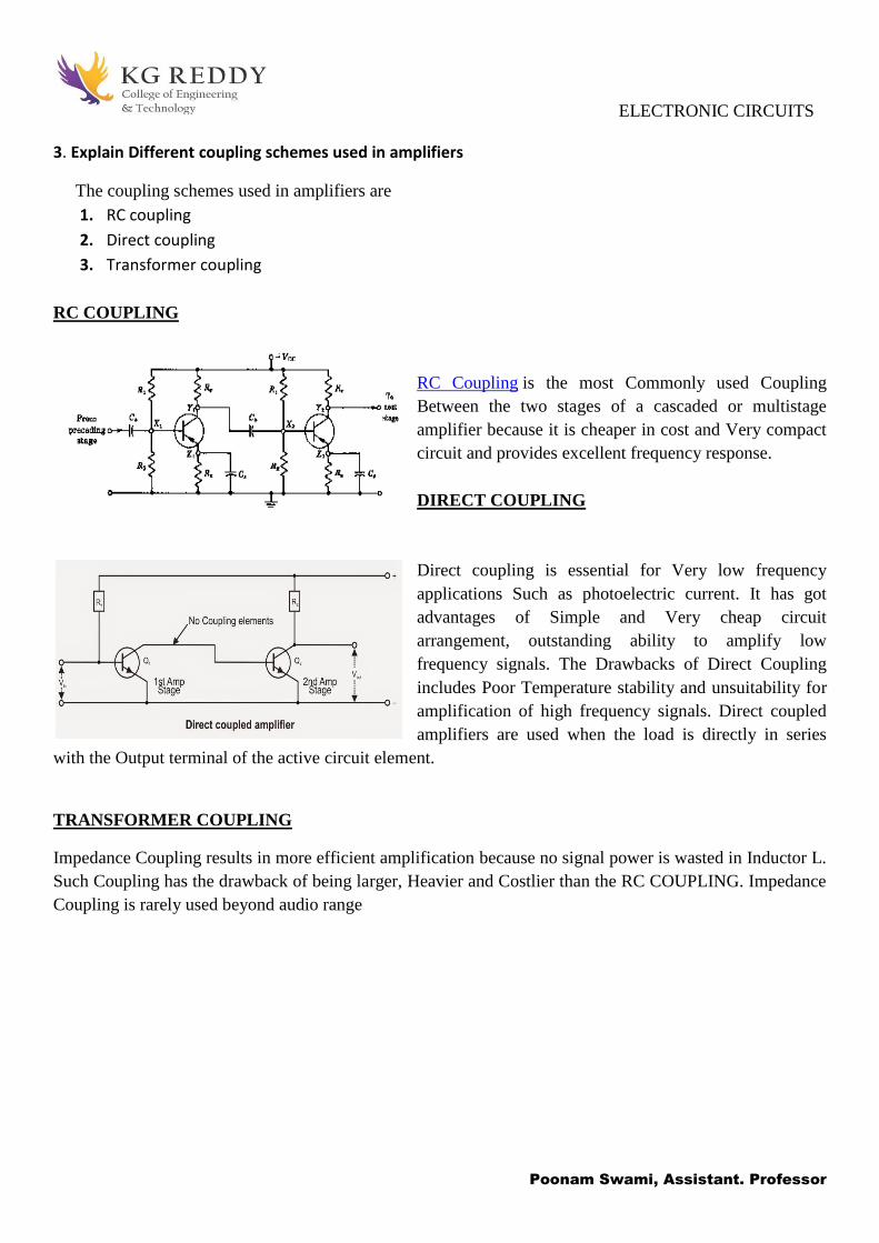
3. Explain Different coupling schemes used in amplifiers
The coupling schemes used in amplifiers are
1. RC coupling
2. Direct coupling
3. Transformer coupling
RC COUPLING
RC Coupling is the most Commonly used Coupling
Between the two stages of a cascaded or multistage
amplifier because it is cheaper in cost and Very compact
circuit and provides excellent frequency response.
DIRECT COUPLING
Direct coupling is essential for Very low frequency
applications Such as photoelectric current. It has got
advantages of Simple and Very cheap circuit
arrangement, outstanding ability to amplify low
frequency signals. The Drawbacks of Direct Coupling
includes Poor Temperature stability and unsuitability for
amplification of high frequency signals. Direct coupled
amplifiers are used when the load is directly in series
with the Output terminal of the active circuit element.
TRANSFORMER COUPLING
Impedance Coupling results in more efficient amplification because no signal power is wasted in Inductor L.
Such Coupling has the drawback of being larger, Heavier and Costlier than the RC COUPLING. Impedance
Coupling is rarely used beyond audio range

ELECTRONIC CIRCUITS
Poonam Swami, Assistant. Professor
4. Explain the comparison of RC coupling, direct coupling and Transformer coupling?
Comparison of above coupling schemes is shown in below table.
S.N Particular R-C Coupled
Amplifier
Transformer
Coupled Amplifier
Direct Coupled
Amplifier
1. Frequency
Response
More Poor best
2. Cost Excellent More Least
3. Space and
Weight
Less More Least
4. Impedance
matching
Not good Good Good
5. Applications Voltage
amplification
Power amplification Amplifying very low
frequencies
5. Explain the operation of Darlington pair?
This is two transistors connected together so that the amplified current from the first is amplified further by
the second transistor. This gives the Darlington pair a very high current gain such as 10000. Darlington pairs
are sold as complete packages containing the two transistors. They have three leads (B, C and E) which are
equivalent to the leads of a standard individual transistor.

ELECTRONIC CIRCUITS
Poonam Swami, Assistant. Professor
The overall current gain is equal to the two individual gains multiplied together:
Darlington pair current gain, hFE = hFE1 × hFE2
(hFE1 and hFE2 are the gains of the individual transistors)
This gives the Darlington pair a very high current gain, such as 10000, so that only a tiny base current is
required to make the pair switch on.
Figure 1: Darlington amplifier Figure 2: Darlington pair
Two transistors may be combined to form a configuration known as the Darlington pair which behaves like
a single transistor with a current gain equivalent to the product of the current gain of the two transistors. This
is especially useful where very high currents need to be controlled as in a power amplifier or power-
regulator circuit. Darlington transistors are available whereby two transistors are combined in one single
package. The base-emitter volt-drop is twice that of a small transistor.
6. Explain the effect of coupling and bypass capacitor on low frequency response of BJT amplifier?
Coupling capacitors (or dc blocking capacitors) are use to decouple ac and dc signals so as not to disturb
the quiescent point of the circuit when ac signals are injected at the input.
Bypass capacitors are used to force signal currents around elements by providing a low impedance path at
the frequency.

ELECTRONIC CIRCUITS
Poonam Swami, Assistant. Professor
7. Explain low frequency response of BJT amplifier?
In the low-frequency region of the single-stage BJT or FET amplifier, it is the R-C combinations formed by
the network capacitors and the network resistive parameters that determine the cutoff frequencies. In fact, an
R-C network similar to the below can be established for each capacitive element and the frequency at which
the output voltage drops to 0.707 of its maximum value determined. Once the cutoff frequencies due to each
capacitor are determined, they can be compared to establish which will determine the low-cutoff frequency
for the system.
Fig (a): R-C combination that will define a low cutoff frequency
(b): R-C circuit at very high frequencies
(c): R-C circuit at low frequency i.e. z = 0
The output and input voltages are related
by the voltage-divider rule in the following
manner:
8. Explain the characteristics of common
collector amplifier and draw it’s small
signal model?
It should be apparent that the load resistor
in the common-collector amplifier circuit
receives both the base and collector
currents, being placed in series with the
emitter. Since the emitter lead of a
transistor is the one handling the most
current (the sum of base and collector
currents, since base and collector currents always mesh together to form the emitter current), it would be
reasonable to presume that this amplifier will have a very large current gain. This presumption is indeed
correct: the current gain for a common-collector amplifier is quite large, larger than any other transistor
amplifier configuration. However, this is not necessarily what sets it apart from other amplifier designs.
ELECTRONIC CIRCUITS
Poonam Swami, Assistant. Professor
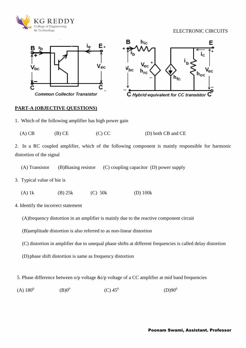
PART-A (OBJECTIVE QUESTIONS)
1. Which of the following amplifier has high power gain
(A) CB (B) CE (C) CC (D) both CB and CE
2. In a RC coupled amplifier, which of the following component is mainly responsible for harmonic
distortion of the signal
(A) Transistor (B)Biasing resistor (C) coupling capacitor (D) power supply
3. Typical value of hie is
(A) 1k (B) 25k (C) 50k (D) 100k
4. Identify the incorrect statement
(A)frequency distortion in an amplifier is mainly due to the reactive component circuit
(B)amplitude distortion is also referred to as non-linear distortion
(C) distortion in amplifier due to unequal phase shifts at different frequencies is called delay distortion
(D) phase shift distortion is same as frequency distortion
5. Phase difference between o/p voltage &i/p voltage of a CC amplifier at mid band frequencies
(A) 1800 (B)00 (C) 450 (D)900

ELECTRONIC CIRCUITS
Poonam Swami, Assistant. Professor
6. Major drawback of Darlington transistor pair [ d ]
(A) low current gain compared to single emitter follower
(B)dependence of Av on transistor selected
(C)low i/p impedance compared to single emitter follower
(D) dependence of H -parameters on quiescent conditions
7. Resultant current gain of a Darlington pair individual current gain of hfe is
(A) hfe/2 (B) 2hfe (C)hfe (D) hfe2
8. 2-stage RC coupled amplifier is configured as
(A) 2 capacitively coupled CE stages cascaded
(B) a CE stage capacitively coupled to a CC stage
(C) 2 capacitively coupled CB stages cascaded.
(D)2 capacitively coupled CC stages cascaded
9. 2-transistor cascade with both collectors tied together & emitter of the transistor connected to the base
of the transistor is referred to as
(A)Darlington pair
(B) CE &CC cascade
(C) cascade amplifier
(D) differential pair
10. the i/p impedance of cascade amplifier is
(A)hic
(B) hie
(C) infinity
(D) hib
PART-A KEY
1 2 3 4 5 6 7 8 9 10
B A A D B D D A A B

ELECTRONIC CIRCUITS
Poonam Swami, Assistant. Professor
PART-B(FILL IN THE BLANKS)
1. The parameter h22 has units of ____________
2. A CC Amplifier has highest ___________ but lowest ___________
3. The current gain of single stage CE amplifier is nearly equal to ________
4. The input impedance Ri of a CE amplifier in terms of hie, hoe, hre and load resistance.
___________________.
5. The phase difference between output and input voltages of a CB amplifier is ________
6. Transformer coupling is generally used when RL is _______
7. In a two stage cascaded amplifier, each of two cascaded stages has a voltage gain of 30 then the overall
gain is ____________
8. The main advantage of multi stage amplifiers is _______
9. Cascode amplifier is a combination of ________
10. Darlington pair is combination of ___________
PART-B KEY
1 Siemens
2 Current gain, power gain
3 Beta
4 hie-(hrehfeRL)/(1+hoeRL)
5 0
6 small
7 900
8 High gain
9 CE-CB
10 CC-CC

ELECTRONIC CIRCUITS
Poonam Swami, Assistant. Professor
Unit 2
a) 2 marks 5 questions with answer
1. List the names of classification of amplifier based on feedback?
The amplifiers are divided into four types
1 .voltage amplifiers
2. Current amplifiers
3. Transconductance amplifier
4. Transresistance amplifier
2. What is feedback?
Feedback is defined as the process in which a part of output signal (voltage or current) is returned back to
the input. The amplifier that operates on the principle of feedback is known as feedback amplifier.
3. What are the types of feedback?
The types of feedbacks are.
1. Positive feedback
2. Negative feedback.
Positive feedback: If the original input signal and the feedback signal are in phase, the feedback is called as
positive feedback.
Negative feedback: However if these two signals are out of phase then the feedback is called as negative
feedback.
3. What are the advantages and disadvantages of negative feedback?
ADVANTAGES
Input resistance increases
Output resistance decreases
Bandwidth increases
Non linear distortion decreases
Frequency distortion decreases

ELECTRONIC CIRCUITS
Poonam Swami, Assistant. Professor
Sensitivity will be decreased
Gain stability
DISADVANTAGES
Decrease in gain
5. What is the effect of negative feedback on input-output resistance?
• Input resistance
Feedback amplifiers, series mixing at the input tends to increase the input resistance and shunt mixing
tends to decrease the input resistance.
• Output resistance
Feedback amplifiers, voltage sampling at the output tends to decrease the output resistance and current
sampling tends to increase the output resistance.
b) 3 marks 5 questions with answer
1. Draw the circuit of voltage shunt feedback amplifier?
2. What is the condition for oscillations?
The use of positive feedback is useful for producing oscillators. The condition for positive feedback is that a
portion of the output is combined in phase with the input. For an amplifer with positive feedback the gain is
given by the expression below

ELECTRONIC CIRCUITS
Poonam Swami, Assistant. Professor
The large open loop gain of an op-amp makes it inevitable that the condition
and the gain expression
Becomes infinite
4. What are the advantages of RC phase shift oscillator
This circuit is very simple and cheap as it comprises resistors and capacitors (not bulky and expensive
high-value inductors).
It provides good frequency stability.
The output of this circuit is sinusoidal that is quite distortion free.
The phase shift oscillator circuit is simpler than the Wein bridge oscillator circuit because it does not
need negative feedback and the stabilization arrangements.
They have a wide range of frequency (from a few Hz to several hundred of kHz).
They are particularly apt for low frequencies, say of the order of 1 Hz, so these frequencies can be easily
gained by using R and C of large values.
4. What is piezo electric effect?
When a voltage source is applied to a small thin piece of quartz crystal, it begins to change shape producing
a characteristic known as the Piezo-electric effect. This Piezo-electric Effect is the property of a crystal by
which an electrical charge produces a mechanical force by changing the shape of the crystal and vice versa,
a mechanical force applied to the crystal produces an electrical charge.
5. What is de-sensitivity factor?
De sensitivity factor is defined as the factor with which the feedback desensitizes the gain. It is also called as
return difference. Sensitivity factor = (dAfb/Afb)/(dA/A) = 1/(1+A*β)
Where Afb is gain with feedback
A is gain without feedback
β is feedback factor.

ELECTRONIC CIRCUITS
Poonam Swami, Assistant. Professor
c) 2 marks 5 questions with answer
1. Explain the classification of amplifiers ?
The classification of amplifiers is
• Voltage Amplifier- An amplifier provides a voltage output proportional to the voltage input and the
proportionality factor does not depend on the magnitudes of the source and load resistance
• Current Amplifier- An amplifier which provides an output current proportional to the signal current .
• Transconductance Amplifier- An amplifier in which, the output current is proportional to the signal
voltage, independent of the magnitudes of source and load resistance.
• Transresistance Amplifier- An amplifier in which output voltage is proportional to the signal current
of the magnitudes of source and load resistance.
2. In a series shunt feedback amplifier shown in below figure calculate the voltage gain without
feedback A and with feedback AFB. ?

ELECTRONIC CIRCUITS
Poonam Swami, Assistant. Professor
3. Explain the Hartley oscillator and colpitts oscillator circuit operations?
Hartley oscillator:
Hartley oscillator is a type of LC oscillator where the
tank circuit consists of two inductors and one capacitor.
The inductors are connected in series and the capacitor is
connected in parallel to the series combination. It was
invented by American scientist Ralph Hartley in 1915.
Typical operating frequency of Hartley oscillator is from
20KHz to 20MHz and it can be realized using BJT, FET
or opamps. The circuit diagram of a Hartley oscillator is
shown in the figure .

ELECTRONIC CIRCUITS
Poonam Swami, Assistant. Professor
Colpitt’s oscillator:
Colpitt’s oscillator is another type of LC oscillator where the tank
circuit consists of two capacitors and one inductor. The capacitors
are connected in series and the inductor is connected in parallel to
the series combination of the capacitors. It was invented by scientist
Edwin Colpitt’s in the year 1918. Typical operating range of
Colpitt’s oscillator is from 20 KHz to MHz The Colpitt’s oscillator
has better frequency stability when compared to Hartley oscillator.
Circuit diagram of a typical Colpitt’s oscillator is shown in the
figure.
4. Show that the gain of Wien bridge oscillator using BJT amplifier must be at least 3 for the
oscillations to occur?
It employs two transistors, each producing a phase shift of 180°, and thus producing a total phase-shift
of 360° or 0°. The circuit diagram of Wien bridge oscillator is shown in the figure below. It is
essentially a two-stage amplifier with an R-C bridge circuit.

ELECTRONIC CIRCUITS
Poonam Swami, Assistant. Professor
5. Draw the circuit diagram of RC phase shift oscillator using BJT.derive the expression for frequency
of oscillations?
In oscillators, RC phase-shift networks, each offering a definite phase-shift can be cascaded so as to satisfy
the phase-shift condition led by the Barkhausen Criterion. One such example is the case in which RC phase-
shift oscillator is formed by cascading three RC phase-shift networks, each offering a phase-shift of 60o, as
shown by Figure

ELECTRONIC CIRCUITS
Poonam Swami, Assistant. Professor

ELECTRONIC CIRCUITS
Poonam Swami, Assistant. Professor
6. Draw the feedback topologies?
7. Explain the characteristics of crystal oscillator?
To obtain a very high level of oscillator stability a Quartz Crystal is generally used as the frequency
determining device to produce other types of oscillator circuit known generally as a Quartz Crystal
Oscillator, (XO).
When a voltage source is applied to a small thin piece of quartz crystal, it begins to change shape producing
a characteristic known as the Piezo-electric effect. This Piezo-electric Effect is the property of a crystal by
which an electrical charge produces a mechanical force by changing the shape of the crystal and vice versa,
a mechanical force applied to the crystal produces an electrical charge.
The equivalent electrical circuit for the quartz crystal shows a series RLC circuit, which represents the
mechanical vibrations of the crystal, in parallel with a capacitance; Cp which represents the electrical
connections to the crystal. Quartz crystal oscillators tend to operate towards their “series resonance”.
The crystals characteristic or characteristic frequency is inversely proportional to its physical thickness
between the two metalized surfaces. A mechanically vibrating crystal can be represented by an equivalent
electrical circuit consisting of low resistance R, a large inductance L and small capacitance C as shown
below
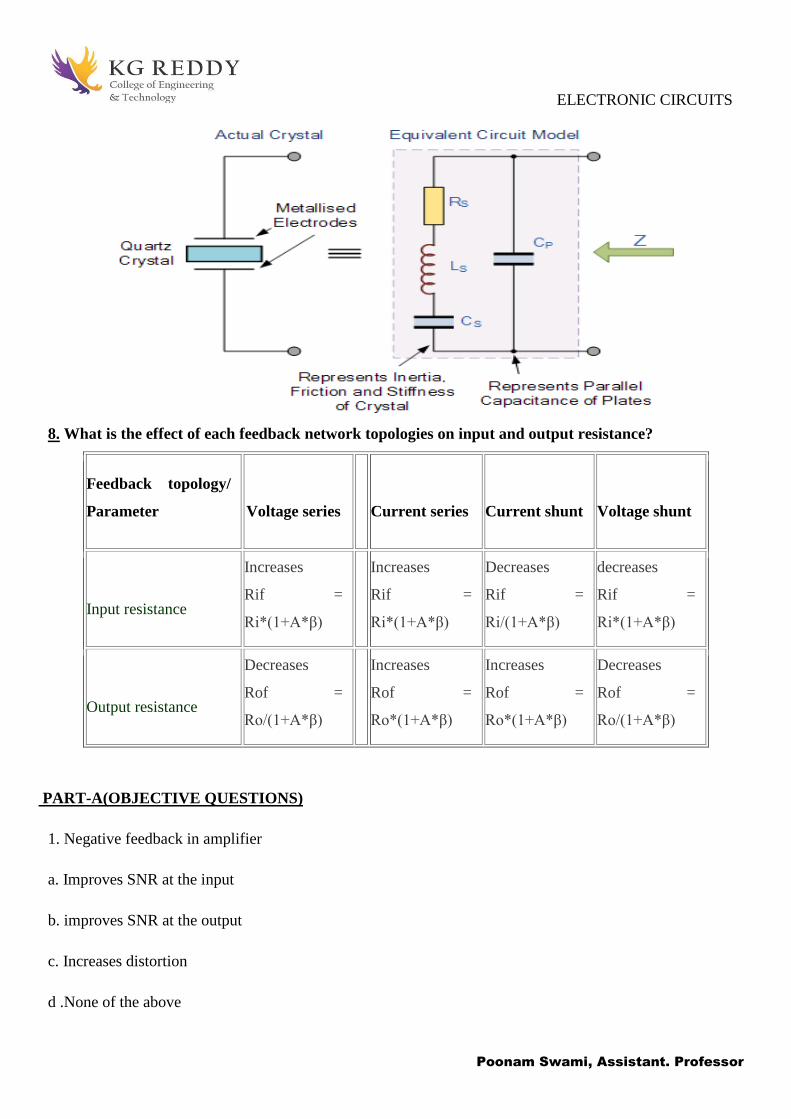
ELECTRONIC CIRCUITS
Poonam Swami, Assistant. Professor
8. What is the effect of each feedback network topologies on input and output resistance?
Feedback topology/
Parameter Voltage series Current series Current shunt Voltage shunt
Input resistance
Increases
Rif =
Ri*(1+A*β)
Increases
Rif =
Ri*(1+A*β)
Decreases
Rif =
Ri/(1+A*β)
decreases
Rif =
Ri*(1+A*β)
Output resistance
Decreases
Rof =
Ro/(1+A*β)
Increases
Rof =
Ro*(1+A*β)
Increases
Rof =
Ro*(1+A*β)
Decreases
Rof =
Ro/(1+A*β)
PART-A(OBJECTIVE QUESTIONS)
1. Negative feedback in amplifier
a. Improves SNR at the input
b. improves SNR at the output
c. Increases distortion
d .None of the above

ELECTRONIC CIRCUITS
Poonam Swami, Assistant. Professor
2. The gain of an amplifier with feedback is ______.
a. A/1+Aβ b. β/1+βa c. β/1-βa d. A/1-Aβ
3. In voltage shunt feedback, the input impedance
a. increases
b. decreases
c. depends on dc voltage applied
d. depends on frequency of operation
4. An oscillator of LC type having a split capacitor in the tank circuit is
a. Hartley b. Colpitts c. Tuned d. Wein Bridge
5. In a Crystal oscillator the frequency is very stable due to ___________ of the crystal
a. rigidity b. high Q c. vibration d. none
6. For generating a sinusoidal wave of 1KHz frequency, the most suitable oscillator is ___
a. Hartley b. Colpitts c. Wien bridge d. None of the above
7. The frequency stability of LC oscillator is _______ than RC oscillators.
a.less b .more c.either a or b d. None of the above
8. An important limitation of a crystal oscillator is ________
a. its low output b. its high Q c. less availability of quartz crystal d. its high output
9. Emitter follower is used because [ ]
a) it’s gain is unity b)it’s gain is high c)it’s output impedance is low d)none
10. Negative feedback in amplifier __________________[ ]
a) Reduces the noise
b) Increases the bandwidth

ELECTRONIC CIRCUITS
Poonam Swami, Assistant. Professor
c) Increases low cutoff frequency
d) Increases the noise
PART A:
1 2 3 4 5 6 7 8 9 10
B A B B C C A A D B
PART-B(FILL IN THE BLANKS)
1. The Trans conductance amplifier is also called as ______________
2. The ratio of input impedance with feedback to without feedback is _________
3. Non sinusoidal oscillators are also called __________
4. The oscillator which uses inductive feedback is ________
5. In a RC phase shift oscillator, each RC section provides a phase shift of _________
6.An oscillator using LC tuned circuit has L= 58.6μH & C=300pF, then the frequency of oscillations will
be ___________
7. Quartz crystal oscillators tend to operate towards their _____________.
8. In current shunt feedback amplifier the output resistance is__________ by a factor of 1+Aβ.
9. one of the effects of negative feedback in amplifier is to __________________
10. The voltage gain of an amplifier is 100.On applying negative feedback with β=0.03,it’s gain will
reduce to_________

ELECTRONIC CIRCUITS
Poonam Swami, Assistant. Professor
PART-B KEY
1 Series series amplifier or current series
amplifier
2 1+Aβ
3 Multi vibrators
4 Hartley
5 600
6 1200KHz
7 Series resonance
8 increased
9 Decrease in harmonic distortion
10 99.97

ELECTRONIC CIRCUITS
Poonam Swami, Assistant. Professor
UNIT 3
a) 2 marks 5 questions with answers
1. What is power amplifier and list the types?
Amplifier circuits form the basis of most electronic systems, many of which need to produce high power to
drive some output device.
Types:
Class A
Class B
Class AB
Class C
2.Define conduction angle in power amplifier?
The time during which the transistor conducts i.e. (the collector current is non zero) when an input
sinusoidal signal is applied in a power amplifier is defined as Conduction angle.
3. What is class A, Class B, Class AB, Class C amplifiers?
Class A amplifier: In class-A amplifiers the collector is biased at a value greater than the amplitude of AC
signal current. Hence the conduction angle is 360 Degrees i.e. the Class A stage conducts for the entire cycle
for the input signal.
Class B amplifier: Class B amplifiers are biased at zero DC bias collector current. Hence it conducts only
for half of the input signal cycle, so the conduction angle for class B amplifier is 180 Degrees.
Class AB amplifier: In class AB amplifiers the biasing current is non zero but much smaller than the peak
current of the sine wave signal. As a result the transistor conducts for interval slightly greater than half a
cycle. The conduction angle is slightly greater than 180 Degrees.
Class C amplifier: In class C amplifier the transistor conducts for an interval less than the half cycle. Hence
the conduction angle is less than 180 Degrees.
4. What is push-pull amplifier?
A push pull amplifier is a special type of arrangement used in class B amplifiers where the active device pair
push (supply) current and pull (absorb) current from load. Push pull amplifiers are more efficient than the
single ended power amplifiers. Because of the symmetric construction of two sides of the amplifier the even

ELECTRONIC CIRCUITS
Poonam Swami, Assistant. Professor
harmonics are cancelled and output signal distortion can be minimized. Another advantage of the push pull
amplifier is the effect of ripple voltage that may be contained in the power supply is balanced out. The main
disadvantages of the push pull amplifier are the need for two identical transistors and the requirement of
bulky and costly coupling transformers used for phase splitting.
5. What is complementary push-pull amplifier?
Complementary Push-pull amplifiers use two “complementary” or matching transistors, one being an NPN-
type and the other being a PNP-type with both power transistors receiving the same input signal together
that is equal in magnitude, but in opposite phase to each other. This results in one transistor only amplifying
one half of the input waveform cycle while the other transistor amplifies the other half of the input
waveform cycle with the resulting “two-halves” being put back together again at the output terminal. In
complementary push pull amplifier neither an input nor an output transformer is needed. The main difficulty
with this circuit .if there is unbalance in the characteristic f the two transistors considerable distortion will be
introduced.
a) 2 marks 5 questions with answers
1.draw the circuit of class A power amplifier?
2. what are the characteristics of Class B Amplifier
The class B amplifiers are the positive and negative halves of the signals, that are allocated to the
different parts of the circuits and the output device switched ON and OFF continuously. The basic
class B amplifiers are used in two complementary transistors which are FET and bipolar. These two

ELECTRONIC CIRCUITS
Poonam Swami, Assistant. Professor
transistors of each half of the waveform with its output are configured in a push-pull type arrangement.
Hence the each amplifier only half of the output waveform.
3. What is cross over distortion?
The main problem with class B push pull output stages is that each transistor conducts for NOT QUITE half
a cycle. As shown in below figure distortion occurs on each cycle of the signal waveform as the input signal
waveform passes through zero volts. Because the transistors have no base bias, they do not actually begin to
conduct until their base/emitter voltage has risen to about 0.6V. As a result, there is a ‘Dead Zone’ of about
1.2V around the zero volts line (between −0.6V and +0.6V) where the signal waveform is not amplified,
causing a "missing" section from the output signal, resulting in unwanted distortion during the "crossover"
from one transistor to the other.
4. What is the effect of each feedback network topologies on input and output resistance?
Feedback
topology/
Parameter
Voltage
series
Current
series
Current
shunt
Voltage
shunt
Input resistance
Increases
Rif =
Ri*(1+A*β)
Increases
Rif =
Ri*(1+A*β)
Decreases
Rif =
Ri/(1+A*β)
decreases
Rif =
Ri*(1+A*β)
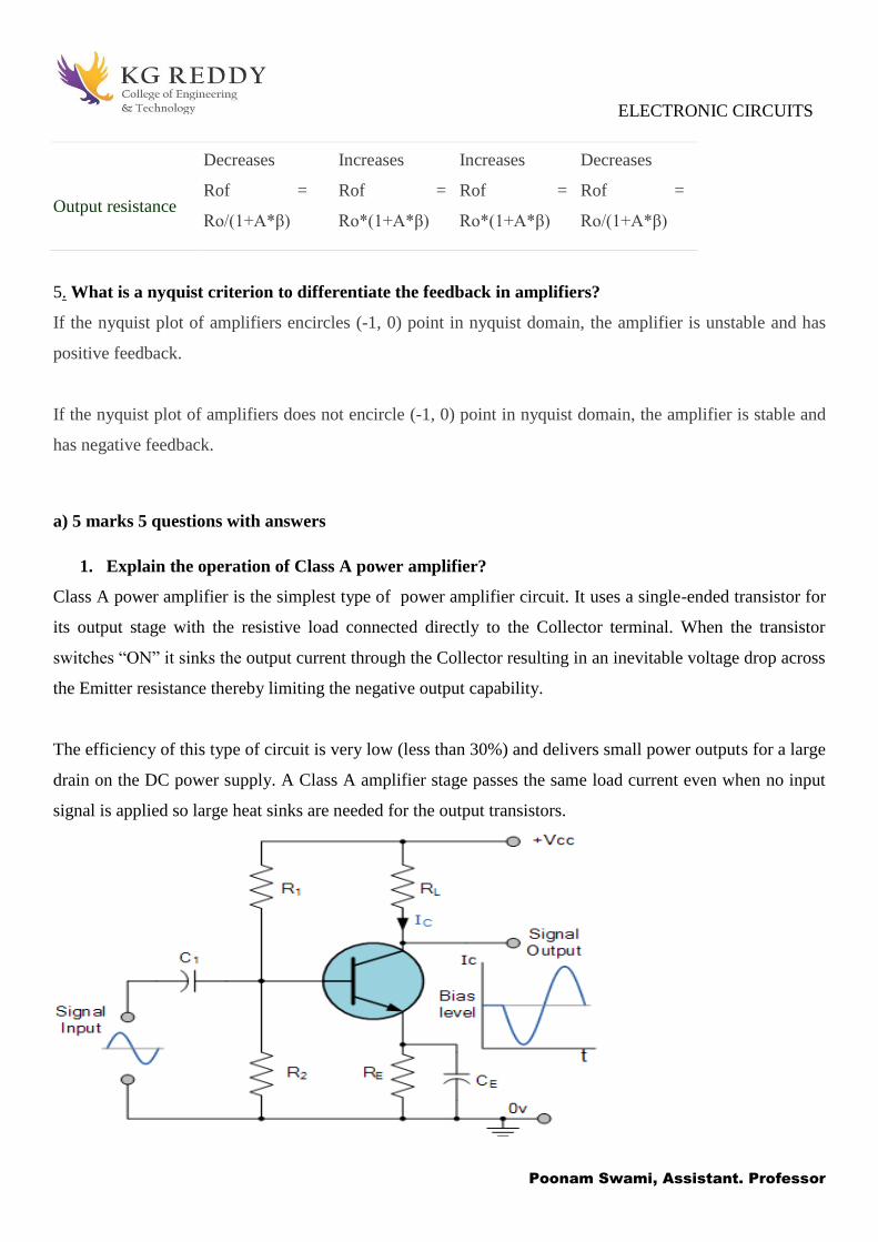
ELECTRONIC CIRCUITS
Poonam Swami, Assistant. Professor
Output resistance
Decreases
Rof =
Ro/(1+A*β)
Increases
Rof =
Ro*(1+A*β)
Increases
Rof =
Ro*(1+A*β)
Decreases
Rof =
Ro/(1+A*β)
5. What is a nyquist criterion to differentiate the feedback in amplifiers?
If the nyquist plot of amplifiers encircles (-1, 0) point in nyquist domain, the amplifier is unstable and has
positive feedback.
If the nyquist plot of amplifiers does not encircle (-1, 0) point in nyquist domain, the amplifier is stable and
has negative feedback.
a) 5 marks 5 questions with answers
1. Explain the operation of Class A power amplifier?
Class A power amplifier is the simplest type of power amplifier circuit. It uses a single-ended transistor for
its output stage with the resistive load connected directly to the Collector terminal. When the transistor
switches “ON” it sinks the output current through the Collector resulting in an inevitable voltage drop across
the Emitter resistance thereby limiting the negative output capability.
The efficiency of this type of circuit is very low (less than 30%) and delivers small power outputs for a large
drain on the DC power supply. A Class A amplifier stage passes the same load current even when no input
signal is applied so large heat sinks are needed for the output transistors.
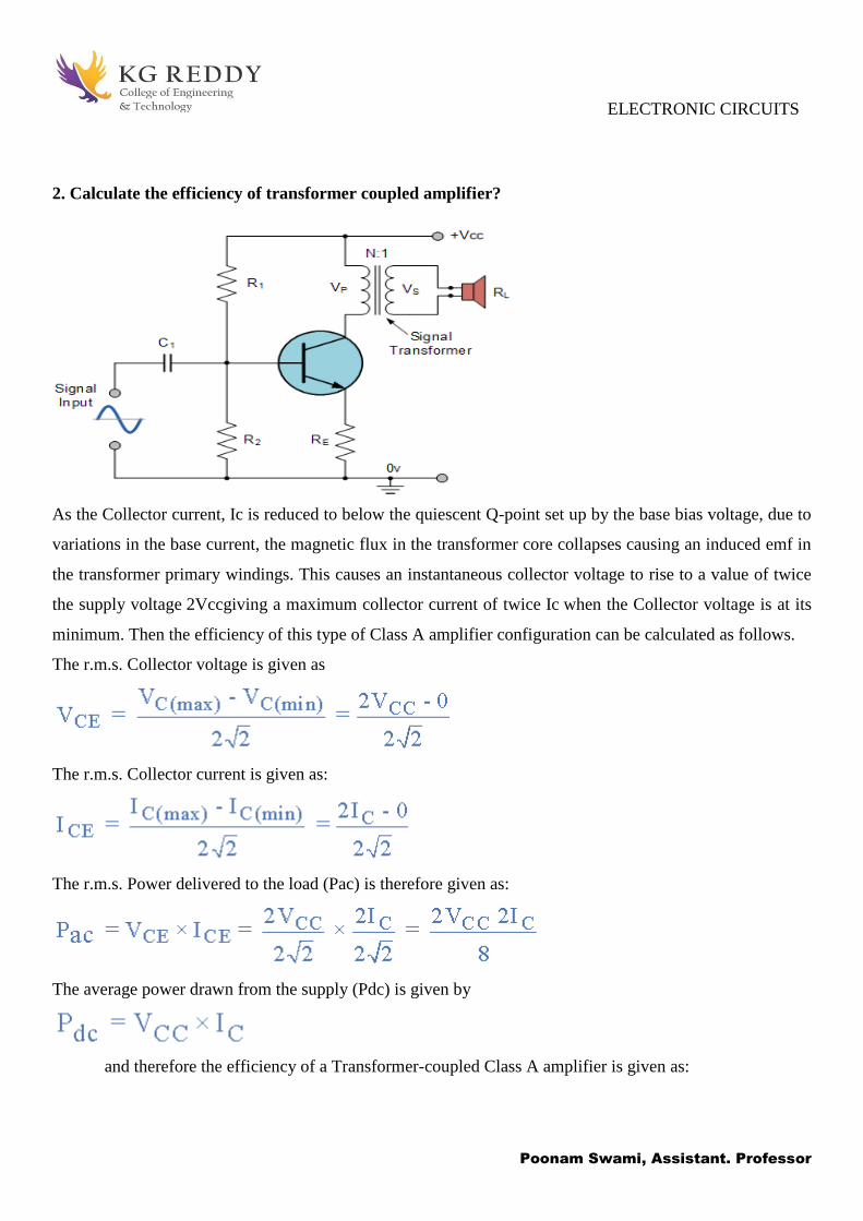
ELECTRONIC CIRCUITS
Poonam Swami, Assistant. Professor
2. Calculate the efficiency of transformer coupled amplifier?
As the Collector current, Ic is reduced to below the quiescent Q-point set up by the base bias voltage, due to
variations in the base current, the magnetic flux in the transformer core collapses causing an induced emf in
the transformer primary windings. This causes an instantaneous collector voltage to rise to a value of twice
the supply voltage 2Vccgiving a maximum collector current of twice Ic when the Collector voltage is at its
minimum. Then the efficiency of this type of Class A amplifier configuration can be calculated as follows.
The r.m.s. Collector voltage is given as
The r.m.s. Collector current is given as:
The r.m.s. Power delivered to the load (Pac) is therefore given as:
The average power drawn from the supply (Pdc) is given by
and therefore the efficiency of a Transformer-coupled Class A amplifier is given as:
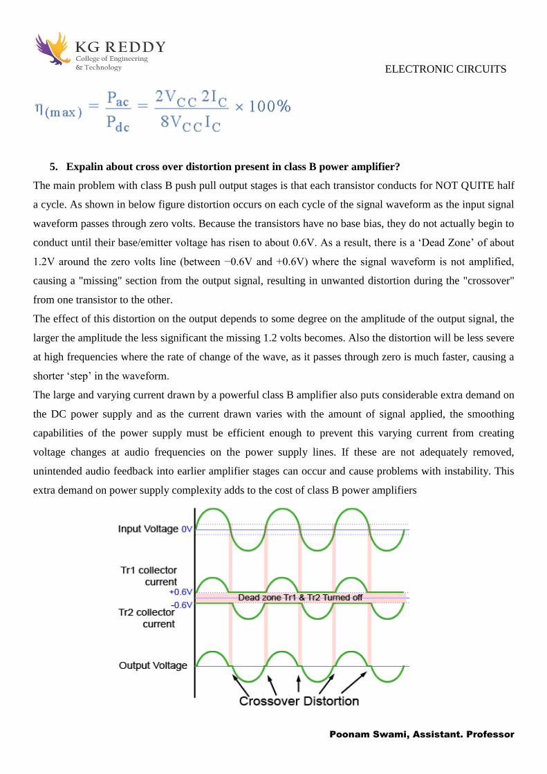
ELECTRONIC CIRCUITS
Poonam Swami, Assistant. Professor
5. Expalin about cross over distortion present in class B power amplifier?
The main problem with class B push pull output stages is that each transistor conducts for NOT QUITE half
a cycle. As shown in below figure distortion occurs on each cycle of the signal waveform as the input signal
waveform passes through zero volts. Because the transistors have no base bias, they do not actually begin to
conduct until their base/emitter voltage has risen to about 0.6V. As a result, there is a ‘Dead Zone’ of about
1.2V around the zero volts line (between −0.6V and +0.6V) where the signal waveform is not amplified,
causing a "missing" section from the output signal, resulting in unwanted distortion during the "crossover"
from one transistor to the other.
The effect of this distortion on the output depends to some degree on the amplitude of the output signal, the
larger the amplitude the less significant the missing 1.2 volts becomes. Also the distortion will be less severe
at high frequencies where the rate of change of the wave, as it passes through zero is much faster, causing a
shorter ‘step’ in the waveform.
The large and varying current drawn by a powerful class B amplifier also puts considerable extra demand on
the DC power supply and as the current drawn varies with the amount of signal applied, the smoothing
capabilities of the power supply must be efficient enough to prevent this varying current from creating
voltage changes at audio frequencies on the power supply lines. If these are not adequately removed,
unintended audio feedback into earlier amplifier stages can occur and cause problems with instability. This
extra demand on power supply complexity adds to the cost of class B power amplifiers

ELECTRONIC CIRCUITS
Poonam Swami, Assistant. Professor
6. Write the classification of power amplifiers
Power Amplifier Classes
Class A B C AB
Conduction
Angle 360o 180o Less than 90o 180 to 360o
Position of
the Q-point
Centre Point of
the Load Line
Exactly on the
X-axis
Below the
X-axis
In between the
X-axis and the
Centre Load Line
Overall
Efficiency
Poor
25 to 30%
Better
70 to 80%
Higher
than 80%
Better than A
but less than B
50 to 70%
Signal
Distortion
None if Correctly
Biased
At the X-axis
Crossover Point Large Amounts Small Amounts
Badly designed amplifiers especially the Class “A” types may also require larger power transistors, more
expensive heat sinks, cooling fans, or even an increase in the size of the power supply required to deliver the
extra power required by the amplifier. Power converted into heat from transistors, resistors or any other
component for that matter, makes any electronic circuit inefficient and will result in the premature failure of
the device.
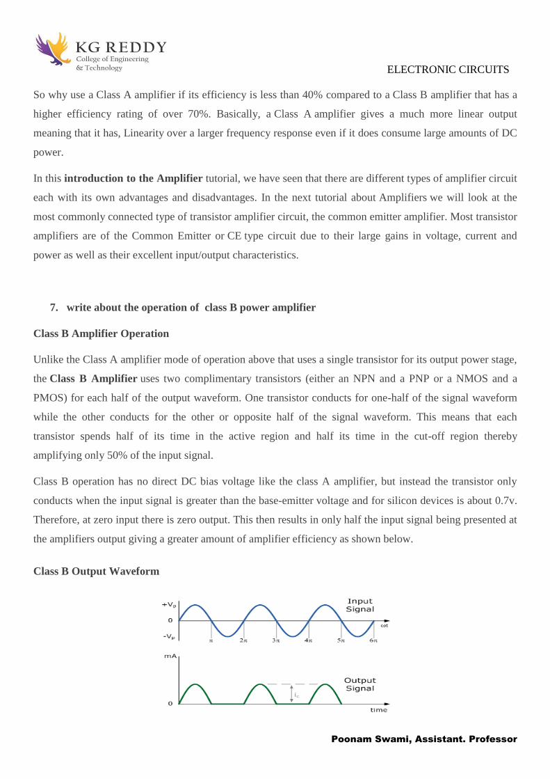
ELECTRONIC CIRCUITS
Poonam Swami, Assistant. Professor
So why use a Class A amplifier if its efficiency is less than 40% compared to a Class B amplifier that has a
higher efficiency rating of over 70%. Basically, a Class A amplifier gives a much more linear output
meaning that it has, Linearity over a larger frequency response even if it does consume large amounts of DC
power.
In this introduction to the Amplifier tutorial, we have seen that there are different types of amplifier circuit
each with its own advantages and disadvantages. In the next tutorial about Amplifiers we will look at the
most commonly connected type of transistor amplifier circuit, the common emitter amplifier. Most transistor
amplifiers are of the Common Emitter or CE type circuit due to their large gains in voltage, current and
power as well as their excellent input/output characteristics.
7. write about the operation of class B power amplifier
Class B Amplifier Operation
Unlike the Class A amplifier mode of operation above that uses a single transistor for its output power stage,
the Class B Amplifier uses two complimentary transistors (either an NPN and a PNP or a NMOS and a
PMOS) for each half of the output waveform. One transistor conducts for one-half of the signal waveform
while the other conducts for the other or opposite half of the signal waveform. This means that each
transistor spends half of its time in the active region and half its time in the cut-off region thereby
amplifying only 50% of the input signal.
Class B operation has no direct DC bias voltage like the class A amplifier, but instead the transistor only
conducts when the input signal is greater than the base-emitter voltage and for silicon devices is about 0.7v.
Therefore, at zero input there is zero output. This then results in only half the input signal being presented at
the amplifiers output giving a greater amount of amplifier efficiency as shown below.
Class B Output Waveform

ELECTRONIC CIRCUITS
Poonam Swami, Assistant. Professor
In a class B amplifier, no DC voltage is used to bias the transistors, so for the output transistors to start to
conduct each half of the waveform, both positive and negative, they need the base-emitter voltage Vbe to be
greater than the 0.7v required for a bipolar transistor to start conducting.
Then the lower part of the output waveform which is below this 0.7v window will not be reproduced
accurately resulting in a distorted area of the output waveform as one transistor turns “OFF” waiting for the
other to turn back “ON”. The result is that there is a small part of the output waveform at the zero voltage
cross over point which will be distorted. This type of distortion is called Crossover Distortion and is looked
at later on in this section.
6. Draw and explain Class AB Amplifier Operation
The Class AB Amplifier is a compromise between the Class A and the Class B configurations above. While
Class AB operation still uses two complementary transistors in its output stage a very small biasing voltage
is applied to the Base of the transistor to bias it close to the Cut-off region when no input signal is present.
An input signal will cause the transistor to operate as normal in its Active region thereby eliminating any
crossover distortion which is present in class B configurations. A small Collector current will flow when
there is no input signal but it is much less than that for the Class A amplifier configuration.
This means then that the transistor will be “ON” for more than half a cycle of the waveform. This type of
amplifier configuration improves both the efficiency and linearity of the amplifier circuit compared to a pure
Class A configuration.
Class AB Output Waveform

ELECTRONIC CIRCUITS
Poonam Swami, Assistant. Professor
The class of operation for an amplifier is very important and is based on the amount of transistor bias
required for operation as well as the amplitude required for the input signal. Amplifier classification takes
into account the portion of the input signal in which the transistor conducts as well as determining both the
efficiency and the amount of power that the switching transistor both consumes and dissipates in the form of
wasted heat. Then we can make a comparison between the most common types of amplifier classifications
in the following table.
7.Explain about transistor power dissipation and heat sinks?
TRANSISTOR POWER DISSIPATION
There is not a clear cut difference between ‘ordinary’ transistors used in voltage amplifiers
and power transistors, but generally Power transistors can be categorised as those than can handle
more than 1 Ampere of collector (or Drain in the case of FETs) current.
power transistors can handle larger currents and higher voltages.
they have a different construction to small signal devices.
They must have low output resistances so that they can deliver large currents to the load, a good
junction insulation to withstand high voltages.
They must also be able to dissipate heat very quickly so they do not overheat.
As most heat is generated at the collector/base junction, the area of this junction is made
HEAT SINKS
A heat-sink is designed to remove heat from a transistor
and dissipate it into the surrounding air as efficiently as
possible. Heat-sinks take many different forms, such as
finned aluminium or copper sheets or blocks, often
painted or anodised matt black to help dissipate heat more
quickly. A selection of heat-sinks is illustrated in
Figure.Good physical contact between the transistor and
heat-sink is essential, and a heat transmitting grease (heat-
sink compound) is smeared on the contact area before
clamping the transistor to the heat-sink.
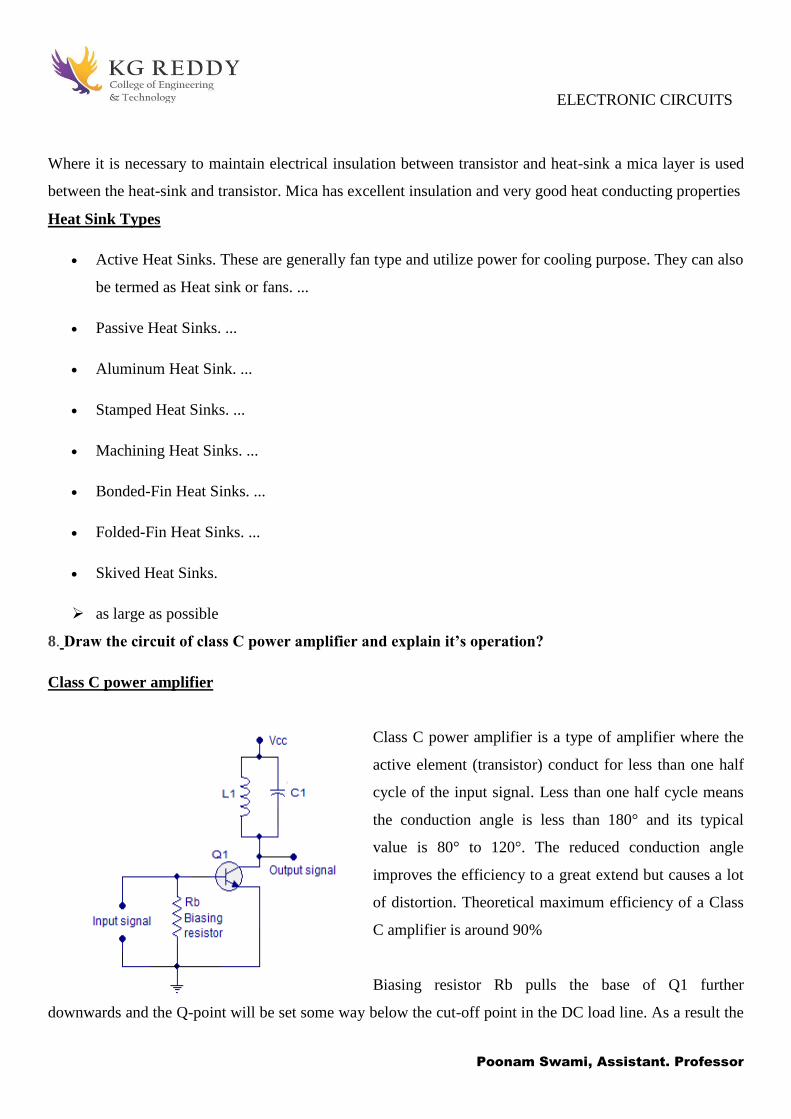
ELECTRONIC CIRCUITS
Poonam Swami, Assistant. Professor
Where it is necessary to maintain electrical insulation between transistor and heat-sink a mica layer is used
between the heat-sink and transistor. Mica has excellent insulation and very good heat conducting properties
Heat Sink Types
Active Heat Sinks. These are generally fan type and utilize power for cooling purpose. They can also
be termed as Heat sink or fans. ...
Passive Heat Sinks. ...
Aluminum Heat Sink. ...
Stamped Heat Sinks. ...
Machining Heat Sinks. ...
Bonded-Fin Heat Sinks. ...
Folded-Fin Heat Sinks. ...
Skived Heat Sinks.
as large as possible
8. Draw the circuit of class C power amplifier and explain it’s operation?
Class C power amplifier
Class C power amplifier is a type of amplifier where the
active element (transistor) conduct for less than one half
cycle of the input signal. Less than one half cycle means
the conduction angle is less than 180° and its typical
value is 80° to 120°. The reduced conduction angle
improves the efficiency to a great extend but causes a lot
of distortion. Theoretical maximum efficiency of a Class
C amplifier is around 90%
Biasing resistor Rb pulls the base of Q1 further
downwards and the Q-point will be set some way below the cut-off point in the DC load line. As a result the
ELECTRONIC CIRCUITS
Poonam Swami, Assistant. Professor
transistor will start conducting only after the input signal amplitude has risen above the base emitter voltage
(Vbe~0.7V) plus the downward bias voltage caused by Rb. That is the reason why the major portion of the
input signal is absent in the output signal
Advantages of Class C power amplifier.
7. High efficiency.
8. Excellent in RF applications.
9. Lowest physical size for a given power output.
Disadvantages of Class C power amplifier.
Lowest linearity.
Not suitable in audio applications.
Creates a lot of RF interference.
It is difficult to obtain ideal inductors and coupling transformers.
Reduced dynamic range.
Applications of Class C power amplifier.
RF oscillators.
RF amplifier.
FM transmitters.
Booster amplifiers.
High frequency repeaters.
Tuned amplifiers etc
9. Explain the effect of Q factor on the performance of the tuned amplifier?
The quality factor or 'Q' of an inductor or tuned circuit is often used to give an indication of its performance
in an RF or other circuit. Values for quality factor are often seen quoted and can be used in defining the
performance of an inductor or tuned circuit.
When dealing with RF tuned circuits, there are many reasons why Q factor is important. Usually a high level
of Q is beneficial, but in some applications a defined level of Q may be what is required.
Some of the considerations associated with Q in RF tuned circuits are summarised below:
Bandwidth: With increasing Q or quality factor, so the bandwidth of the tuned circuit filter is
reduced. As losses decrease so the tuned circuit becomes sharper as energy is stored better in the
circuit. It can be seen that as the Q increases, so the 3 dB bandwidth decreases and the overall
response of the tuned circuit increases.

ELECTRONIC CIRCUITS
Poonam Swami, Assistant. Professor
Ringing: As the Q of a resonant circuit increases so the losses decrease. This means that any
oscillation set up within the circuit will take longer to die away. In other words the circuit will tend
to "ring" more. This is actually ideal for use within an oscillator circuit because it is easier to set up
and maintain an oscillation as less energy is lost in the tuned circuit.
Oscillator phase noise: Any oscillator generates what is known as phase noise. This comprises
random shifts in the phase of the signal. This manifests itself as noise that spreads out from the main
carrier. As might be expected, this noise is not wanted and therefore needs to be minimised. The
oscillator design can be tailored to reduce this in a number of ways, the chief one being by increasing
the Q, quality factor of the oscillator tuned circuit.
General spurious signals: Tuned circuits and filters are often used to remove spurious signals. The
sharper the filter and the higher the level of Q, the better the circuit will be able to remove the
spurious signals.
Wide bandwidth: In many RF applications there is a requirement for wide bandwidth operation.
Some forms of modulation require a wide bandwidth, and other applications require fixed filters to
provide wide band coverage. While high rejection of unwanted signals may be required, there is a
competing requirement for wide bandwidths. Accordingly in many applications the level of Q
required needs to be determined to provide the overall performance that is needed meeting requirements
for wide bandwidth and adequate rejection of unwanted signals.
10. What are the types of small signal tuned amplifier and draw their circuits
SMALL SIGNAL TUNED AMPLIFIERS
Uses one parallel tuned circuit as the load IZI in each stage and all these tuned circuits in different stages
are tuned to the same frequency. To get large Av or Ap, multistage amplifiers are used. But each stage is
tuned to the same frequency, one tuned circuit in one stage.

ELECTRONIC CIRCUITS
Poonam Swami, Assistant. Professor
SINGLE TUNED CAPACITIVE COUPLED AMPLIFIER
SINGLE TUNED TRANSFORMER COUPLED AMPLIFIER
A double-tuned amplifier is a tuned amplifier with transformer coupling between the amplifier stages in
which the inductances of both the primary and secondary windings are tuned separately with
a capacitor across each. The scheme results in a wider bandwidth and steeper skirts than a single tuned
circuit would achieve

ELECTRONIC CIRCUITS
Poonam Swami, Assistant. Professor
PART-A(OBJECTIVE QUESTIONS)
1. With transformer connection to load the maximum efficiency of the class A amplifier will go up to a
maximum of [c ]
a. 78.5% b.25% c.50% d.66%
2. In ____ power amplifier, the output signal varies for a full 3600 of the cycle. [a]
(a)Class A (b) Class B c) Class AB (d) None of the above
3. 4. Maximum theoretical efficiency of Class B push pull amplifier is ___. [d ]
(a)25.5% (b) 50% (c) 75% (d) 78.5%
4. The purpose of resonant circuits in tuned circuits is [d ]
a. To provide properly matching load impedance
b. To reset unwanted harmonics
c. To couple power to load
d. All of the above
5. To reduce further harmonic distortion in large signal tuned amplifiers_______- is used [c ]
a. feedback configuration
b. transformer coupling
c. Push Pull configuration
d. all of the can be used
6. In tuned amplifiers, harmonic distortion is ____________. [c ]
(a) Infinite (b) more (c) less (d) None
7. Double tuned amplifier provides ____ bandwidth than single tuned amplifiers. [ a]
(a)larger (b) smaller (c) negligible (d)constant

ELECTRONIC CIRCUITS
Poonam Swami, Assistant. Professor
8. Tuned amplifiers can be used in _____. [c ]
(a)Radar (b) IF amplifiers (c) both a and b (d) None
9.In classA power amplifier clipping of the positive peak of the output voltage takes place when [ c ]
a) the Q-point is centered on the load line
b) the Q-point is closer to saturation
c)the Q-point is closer to cutoff
d)no clipping takes place.
10._________ signal repeats itself as a regular intervals of time. [ a]
a) periodic signals
b) A periodic signals
c) Random signals
d) None
PART-A
1 2 3 4 5 6 7 8 9 10
B A B B C C A A C A
PART-B (FILL IN THE BLANKS)
1. Thermal resistance of the heat sink will be typically 30 C/W
2. If output power=20W and the input dc power=60W, then the efficiency of power amplifier
is 33.3%
3. In Class B power amplifier, Q-point is set near cutoff
4. The input transformer in push-pull power amplifier is Step-up
5. output transformer in push pull power amplifier is Step down
6. Small signal tuned amplifiers are operated in Class A mode.
7. Parallel tuned circuit is also known as Anti resonant circuit

ELECTRONIC CIRCUITS
Poonam Swami, Assistant. Professor
8. Example of random signal is Noise
9. The maximum p-p collector voltage for the amplifier of Q is 3v
10. The transistor of a large signal amplifier is biased right at cut-off.It operates under the condition of
Class C
PART-B
1 30 C/W
2 33.3%
3 Near cutoff
4 Step-up
5 Step-down
6 Class A mode
7 Anti resonant circuit
8 Noise
9 3v
10 Class C

ELECTRONIC CIRCUITS
Poonam Swami, Assistant. Professor
UNIT 4
a) 2 marks 5 questions with answers
1. Write the working of negative clamping circuit.
Working of Clipper Circuit
The clipper circuit can be designed by utilizing both the linear and nonlinear elements such as resistors,
diodes or transistors. As these circuits are used only for clipping input waveform as per the requirement and
for transmitting the waveform, they do not contain any energy storing element like a capacitor.
In general, clippers are classified into two types: Series Clippers and Shunt Clippers.
1. Series Clippers
Series clippers are again classified into series negative clippers and series positive clippers which are as
follows:
a. Series Negative Clipper
Series Negative Clipper
The above figure shows a series negative clipper with its output waveforms. During the positive half cycle
the diode (considered as ideal diode) appears in the forward biased and conducts such that the entire positive
half half cycle of input appears across the resistor connected in parallel as output waveform. During the
negative half cycle the diode is in reverse biased. No output appears across the resistor. Thus, it clips the
negative half cycle of the input waveform, and therefore, it is called as a series negative clipper.

ELECTRONIC CIRCUITS
Poonam Swami, Assistant. Professor
Series Negative Clipper with Positive Vr
Series Negative Clipper with Positive Vr
Series negative clipper with positive reference voltage is similar to the series negative clipper, but in this a
positive reference voltage is added in series with the resistor. During the positive half cycle, the diode start
conducting only after its anode voltage value exceeds the cathode voltage value. Since cathode voltage
becomes equal to the reference voltage, the output that appears across the resistor will be as shown in the
above figure.
Series Negative Clipper with Negative Vr
The series negative clipper with a negative reference voltage is similar to the series negative clipper with
positive reference voltage, but instead of positive Vr here a negative Vr is connected in series with the
resistor, which makes the cathode voltage of the diode as negative voltage. Thus during the positive half
cycle, the entire input appears as output across the resistor, and during the negative half cycle, the input
appears as output until the input value will be less than the negative reference voltage, as shown in the
figure.
2. working principal of simple diode comparator
An operational amplifier (op-amp) has a well balanced difference input and a very high gain. This parallels
the characteristics of comparators and can be substituted in applications with low-performance
requirements.In theory, a standard op-amp operating in open-loop configuration (without negative feedback)
may be used as a low-performance comparator. When the non-inverting input (V+) is at a higher voltage
than the inverting input (V-), the high gain of the op-amp causes the output to saturate at the highest positive

ELECTRONIC CIRCUITS
Poonam Swami, Assistant. Professor
voltage it can output. When the non-inverting input (V+) drops below the inverting input (V-), the output
saturates at the most negative voltage it can output. The op-amp's output voltage is limited by the supply
voltage. An op-amp operating in a linear mode with negative feedback, using a balanced, split-voltage
power supply, (powered by ± VS). However, this equation may not be applicable to a comparator circuit
which is non-linear and operates open-loop (no negative feedback)
In practice, using an operational amplifier as a comparator presents several disadvantages as compared to
using a dedicated comparator:
Op-amps are designed to operate in the linear mode with negative feedback. Hence, an op-amp typically has
a lengthy recovery time from saturation. Almost all op-amps have an internal compensation capacitor which
imposes slew rate limitations for high frequency signals. Consequently, an op-amp makes a sloppy
comparator with propagation delays that can be as long as tens of microseconds.
Since op-amps do not have any internal hysteresis, an external hysteresis network is always necessary for
slow moving input signals.
The quiescent current specification of an op-amp is valid only when the feedback is active. Some op-amps
show an increased quiescent current when the inputs are not equal.
A comparator is designed to produce well limited output voltages that easily interface with digital logic.
Compatibility with digital logic must be verified while using an op-amp as a comparator.
Some multiple-section op-amps may exhibit extreme channel-channel interaction when used as comparators.
Many op-amps have back to back diodes between their inputs. Op-amp inputs usually follow each other so
this is fine. But comparator inputs are not usually the same. The diodes can cause unexpected current
through inputs.
3. Explain the principle of clamping.
In electronics, a clipper is a device designed to prevent the output of a circuit from exceeding a
predetermined voltage level without distorting the remaining part of the applied waveform A clipping
circuit consists of linear elements like resistors and non-linear elements like junction
diodes or transistors, but it does not contain energy-storage elements like capacitors. Clipping
circuits are used to select for purposes of transmission, that part of a signal wave form which lies above
or below a certain reference voltage level.
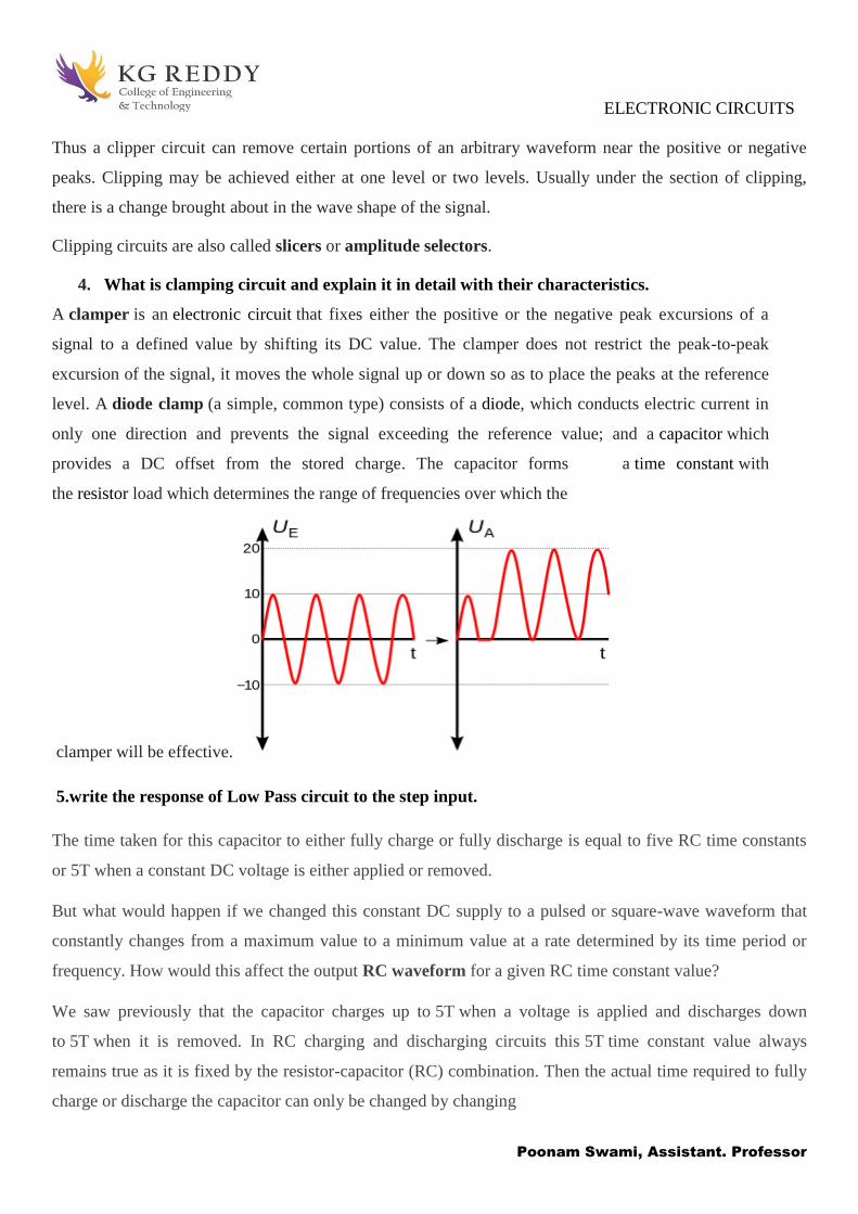
ELECTRONIC CIRCUITS
Poonam Swami, Assistant. Professor
Thus a clipper circuit can remove certain portions of an arbitrary waveform near the positive or negative
peaks. Clipping may be achieved either at one level or two levels. Usually under the section of clipping,
there is a change brought about in the wave shape of the signal.
Clipping circuits are also called slicers or amplitude selectors.
4. What is clamping circuit and explain it in detail with their characteristics.
A clamper is an electronic circuit that fixes either the positive or the negative peak excursions of a
signal to a defined value by shifting its DC value. The clamper does not restrict the peak-to-peak
excursion of the signal, it moves the whole signal up or down so as to place the peaks at the reference
level. A diode clamp (a simple, common type) consists of a diode, which conducts electric current in
only one direction and prevents the signal exceeding the reference value; and a capacitor which
provides a DC offset from the stored charge. The capacitor forms a time constant with
the resistor load which determines the range of frequencies over which the
clamper will be effective.
5.write the response of Low Pass circuit to the step input.
The time taken for this capacitor to either fully charge or fully discharge is equal to five RC time constants
or 5T when a constant DC voltage is either applied or removed.
But what would happen if we changed this constant DC supply to a pulsed or square-wave waveform that
constantly changes from a maximum value to a minimum value at a rate determined by its time period or
frequency. How would this affect the output RC waveform for a given RC time constant value?
We saw previously that the capacitor charges up to 5T when a voltage is applied and discharges down
to 5T when it is removed. In RC charging and discharging circuits this 5T time constant value always
remains true as it is fixed by the resistor-capacitor (RC) combination. Then the actual time required to fully
charge or discharge the capacitor can only be changed by changing

ELECTRONIC CIRCUITS
Poonam Swami, Assistant. Professor
the value of either the capacitor itself or the resistor in the circuit and this is shown below.
b) 3 marks 5 questions with answers
1.Write the response of lowpass filter to ramp input
A low-pass filter is a filter that passes signals with a frequency lower than a certain cutoff
frequency and attenuates signals with frequencies higher than the cutoff frequency. The exact frequency
response of the filter depends on the filter design. The filter is sometimes called a high-cut filter, or treble
cut filter in audio applications. A low-pass filter is the complement of a high-pass filter.
Low-pass filters exist in many different forms, including electronic circuits such as a hiss
filter usedlin audio, anti-aliasing filters for conditioning signals prior to analog-to-digital
conversion, digital filters for smoothing sets of data, acoustic barriers, blurring of images, and so on.
The moving average operation used in fields such as finance is a particular kind of low-pass filter, and can
be analyzed with the same signal processing techniques as are used for other low-pass filters. Low-pass
filters provide a smoother form of a signal, removing the short-term fluctuations, and leaving the longer-
term trend.
Filter designers will often use the low-pass form as a prototype filter. That is, a filter with unity bandwidth
and impedance. The desired filter is obtained from the prototype by scaling for the desired bandwidth and
impedance and transforming into the desired bandform (that is low-pass, highpass, band-pass or band-stop.

ELECTRONIC CIRCUITS
Poonam Swami, Assistant. Professor
2.Write the response of high pass filter to RC integrator
The RC Integrator
The Integrator is a type of Low Pass Filter circuit that converts a square wave input signal into a triangular
waveform output. As seen above, if the 5RC time constant is long compared to the time period of the input
RC waveform the resultant output will be triangular in shape and the higher the input frequency the lower
will be the output amplitude compared to that of the input.
From which we derive an ideal voltage output for the integrator as:
3.write the response of highpass filter to RC differentiator
The RC Differentiator
The Differentiator is a High Pass Filter type of circuit that can convert a square wave input signal into
high frequency spikes at its output. If the 5RC time constant is short compared to the time period of the
input waveform, then the capacitor will become fully charged more quickly before the next change in the
input cycle.
When the capacitor is fully charged the output voltage across the resistor is zero. The arrival of the falling
edge of the input waveform causes the capacitor to reverse charge giving a negative output spike, then as the
square wave input changes during each cycle the output spike changes from a positive value to a negative
value.

ELECTRONIC CIRCUITS
Poonam Swami, Assistant. Professor
from which we have an ideal voltage output for the Differentiator as:
8. Explain negative peak clipper with and without reference voltage.
Negative Diode Clipper
The negative clipping circuit is almost same as the positive clipping circuit, with only one difference. If the
diode in figures (a) and (b) is reconnected with reversed polarity, the circuits will become for a negative
series clipper and negative shunt clipper respectively. The negative series and negative shunt clippers are
shown in figures (a) and (b) as given below.

ELECTRONIC CIRCUITS
Poonam Swami, Assistant. Professor
In all the above discussions, the diode is considered to be ideal one. In a practical diode, the breakdown
voltage will exist (0.7 V for silicon and 0.3 V for Germanium). When this is taken into account, the output
waveforms for positive and negative clippers will be of the shape shown in the figure below.
9. Explain about transistor clippers
The transistor has two types of linearities —One linearity happens when the transistor passes from
cut-in region to the active region. The other linearity occurs when the transistor passes from the
active region to the saturation region. When any input signal passes through the transistor, across the

ELECTRONIC CIRCUITS
Poonam Swami, Assistant. Professor
boundary between cut-in region and active region, or across the boundary between the active region
and saturation region, a portion of the input signal waveform will be clipped off. Portion of the input
waveform which keeps the transistor in the active region shall appear at the output without any
distortion. In such a case, it is the input current rather than the input voltage that should have the
waveform of the signal of interest. Obvious reason is that over a large signal excursion in the active
region, the transistor output current responds linearly to the input current but is related quite
nonlinearly to the input voltage. Therefore, a current drive is used in a transistor clipper, as
illustrated in the figure given below.
In the active region, the value of the resistor RB must be large enough when compared to the input
resistance of the transistor. The input base current will have the waveform of input voltage and iB =
vin – base-to-emitter cut-in voltage / RB Waveforms for the transistor clipper for ramp input are
shown in the figure given below.
In the active region, the value of the resistor RB must be large enough when compared to the input
resistance of the transistor. The input base current will have the waveform of input voltage and iB = vin –
base-to-emitter cut-in voltage / RB Waveforms for the transistor clipper for ramp input are shown in the
figure given below

ELECTRONIC CIRCUITS
Poonam Swami, Assistant. Professor
c) 5 marks 5 questions with answers
1. what is low pass filter?
Low pass filter
A first order, low pass RC filter is simply an RC series circuit across the input, with the output taken across
the capacitor. We assume that the output of the circuit is not connected, or connected only to high
impedance, so that the current is the same in both R and C.
The voltage across the capacitor is IXC = I/ωC. The voltage across the series combination is
IZRC = I(R2 + (1/ωC)2)1/2, so the gain is

ELECTRONIC CIRCUITS
Poonam Swami, Assistant. Professor
From the phasor diagram for this filter, we see that the output lags the
input in phase.
At the angular frequency ω = ωo = 1/RC, the capacitive reactance 1/ωC equals the resistance R. We show
this characteristic frequency* on all graphs on this page. For instance, if R = 1 kω and C = 0.47 F, then
1/RC = ωo = 2.1 103 rad.s-1, so fo = ωo/2π = 340 Hz.
At this frequency, the gain = 1/20.5 = 0.71, as shown on the plot of g(ω). The power transmitted usually goes
as the gain squared, so the filter transmits 50% of maximum power at fo. Now a reduction in power of
a factor of two means a reduction by 3 dB signal with frequency f = fo = 1/2πRC is attenuated by 3 dB,
lower frequencies are less attenuated and high frequencies more attenuated.
At ω = ωo, the phase difference is π/4 radians or 45°, as shown in the plot of φ
At high frequencies, the capacitor 'shorts out' the input to
the sound card, but hardly affects low frequencies. So
this sound is less 'bright' than the example above.
This sound is quieter than the previous sample. We have
cut out the frequencies above 1 kHz, including those to
which your ear is most sensitive. (For more about the
frequency response of the ear, see Hearing Curves.)

ELECTRONIC CIRCUITS
Poonam Swami, Assistant. Professor
2. what is high pass RC circuit
At low frequencies, the reactance of the capacitor is high, so little current goes to the
speaker. This sound is less 'bassy' than those above.
Losing the low frequencies makes the sound rather thin, but it doesn't reduce the loudness
as much as removing the high frequencies.
(If you do not notice much difference with the high pass filter, it may be because you are
using tiny computer speakers that do not radiate low frequencies well. Try it with
headphones or with hifi speakers.)
Filter gains are usually written in decibels. see the decibel scale.
Integrator
Here we have an AC source with voltage vin(t), input to an RC series circuit. The output is the voltage
across the capacitor. We consider only high frequencies ω >> 1/RC, so that the capacitor has
insufficient time to charge up, its voltage is small, so the input voltage approximately equals the voltage
across the resistor.
The photograph at the top of this page shows a triangle wave input to an RC integrator, and the resulting
output.

ELECTRONIC CIRCUITS
Poonam Swami, Assistant. Professor
Differentiator
Again we have an AC source with voltage vin(t), input to an RC series circuit. This time the output is
the voltage across the resistor. This time, we consider only low frequencies ω << 1/RC, so that the
capacitor has time to charge up until its voltage almost equals that of the source.
More accurate integration and differentiation is possible using resistors and capacitors on the input and
feedback loops of operational amplifiers. Such amplifiers can also be used to add, to subtract and to multiply
voltages. An analogue computer is a combination of such circuits, and may be used to solve simultaneous,
differential and integral equations very rapidly.
3. Explain about diode clippers
Most of the electronic circuits like amplifiers, modulators and many others have a particular range of
voltages at which they have to accept the input signals. Any of the signals that have an amplitude greater
than this particular range may cause distortions in the output of the electronic circuits and may even lead to
damage of the circuit components.
In view of the fact that most of the electronic devices work on a single positive supply, the input voltage
range would also be on the positive side. Since the natural signals like audio signals, sinusoidal waveforms
and many others contain both positive and negative cycles with varying amplitude in their duration.
These waveforms and other signals have to be modified in such a way that the single supply electronic
circuits can be able to operate on them.The clipping of a waveform is the most common technique that
applies to the input signals to adapt them so that they may lie within the operating range of the electronic
circuits. The clipping of waveforms can be done by eliminating the portions of the waveform which crosses
the input range of the circuit.
Clippers can be broadly classified into two basic types of circuits. They are: series clippers and shunt or
parallel clippers. Series clipper circuit contains a power diode in series with the load connected at the end of
the circuit. The shunt clipper contains a diode in parallel with the resistive load.The half – wave rectifier
circuit is similar to a series clipper circuit. If the diode in series clipper circuit is in forward bias condition,
the output waveform at the load follows the input waveform. When the diode is in reverse bias and it is
unable to conduct current, the output of the circuit is nearly zero volts.

ELECTRONIC CIRCUITS
Poonam Swami, Assistant. Professor
The direction of the connected diode determines the polarity of the clipped output waveform. If the diode
symbol points toward the source and is connected to the positive terminal of the supply, the circuit will be a
positive series clipper, resembles that it clips off the positive alternation or cycle of the input sinusoidal
waveform.
If the diode symbol points toward the connected load, then the circuit will be a negative series clipper,
resembles that it clips off the negative alternation or cycle of the input sinusoidal waveform.The series
clipper diode has an output voltage of VLoad = VInput, when the diode is conducting, and when it is not
conducting the input voltage applied by the supply will be dropped and has an output voltage of VLoad = 0
Volts.
In contrast to the series clipper circuit, a shunt clipper circuit provides the output when the diode is
connected in reverse bias and when it is not conducting. When the diode is non – conducting, the shunt
combination diode acts as an open circuit and both the series resistor and load resistor acts as a voltage
divider. The output voltage will be calculated as
VLoad = VInput {RLoad / (RLoad + RSeries)}
When the diode is conducting, it acts as a short circuit and the output voltage across the load will be VLoad =
0 Volts. The series limiting resistor is connected in series with the supply to prevent the diode from short
circuits.

ELECTRONIC CIRCUITS
Poonam Swami, Assistant. Professor
In this case, the output voltage of the circuit should be ±0.7 volts. It depends on the polarity of the shunt
clipper which is determined by the direction of diode connection.Above biased clipper circuit is a shunt clipper
circuit which uses the DC supply voltage to bias the diode. It is the biasing voltage at which the diode starts
conducting. The diode in the shunt clipper circuit starts to conduct when it reaches the biasing voltage. Clipper
circuits are used in a variety of systems to perform one of the two functions:
1. Altering the waveform shapes
2. Protecting the circuits from transients
The first application is commonly noticed in the operation of half-wave rectifiers that changes the varying
voltage into an output pulsative DC waveform. A transient is defined as an abrupt change in current or
voltage with extremely short duration. Clipper circuits can be used to protect the sensitive circuits from
transient effects.
Above biased clipper circuit is a shunt clipper circuit which uses the DC supply voltage to bias the diode. It
is the biasing voltage at which the diode starts conducting. The diode in the shunt clipper circuit starts to
conduct when it reaches the biasing voltage. Clipper circuits are used in a variety of systems to perform one
of the two functions:
1. Altering the waveform shapes
2. Protecting the circuits from transients
The first application is commonly noticed in the operation of half-wave rectifiers that changes the varying
voltage into an output pulsating DC waveform. A transient is defined as an abrupt change in current or
voltage with extremely short duration. Clipper circuits can be used to protect the sensitive circuits from
transient effects.

ELECTRONIC CIRCUITS
Poonam Swami, Assistant. Professor
,
4 . Give the circuits of different types of shunt clippers and explain their operation
Shunt clippers: In shunt clippers, the diode is connected in parallel with the output. Depending on diode
connection shunt clippers are divided into two types
Positive shunt clipper: During positive half cycle of input voltage is positive therefore diode is forward
biased and act as closed switch hence all the current flows through the diode and no voltage drop across the
output and output is zero. During negative half cycle input voltage is negative hence diode is reverse biased
and act as open switch hence there is direct connection between input and output hence during negative half
we get output waveform as shown in Fig3 (b)
Fig3 (a) circuit diagram (b) output waveform for sine wave input
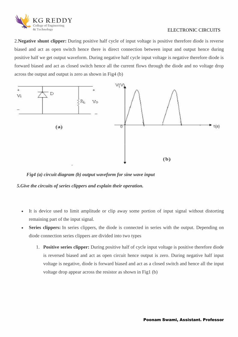
ELECTRONIC CIRCUITS
Poonam Swami, Assistant. Professor
2.Negative shunt clipper: During positive half cycle of input voltage is positive therefore diode is reverse
biased and act as open switch hence there is direct connection between input and output hence during
positive half we get output waveform. During negative half cycle input voltage is negative therefore diode is
forward biased and act as closed switch hence all the current flows through the diode and no voltage drop
across the output and output is zero as shown in Fig4 (b)
Fig4 (a) circuit diagram (b) output waveform for sine wave input
5.Give the circuits of series clippers and explain their operation.
It is device used to limit amplitude or clip away some portion of input signal without distorting
remaining part of the input signal.
Series clippers: In series clippers, the diode is connected in series with the output. Depending on
diode connection series clippers are divided into two types
1. Positive series clipper: During positive half of cycle input voltage is positive therefore diode
is reversed biased and act as open circuit hence output is zero. During negative half input
voltage is negative, diode is forward biased and act as a closed switch and hence all the input
voltage drop appear across the resistor as shown in Fig1 (b)
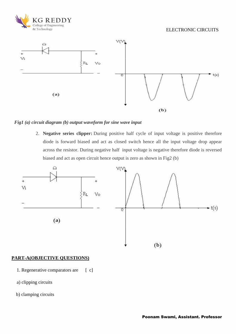
ELECTRONIC CIRCUITS
Poonam Swami, Assistant. Professor
Fig1 (a) circuit diagram (b) output waveform for sine wave input
2. Negative series clipper: During positive half cycle of input voltage is positive therefore
diode is forward biased and act as closed switch hence all the input voltage drop appear
across the resistor. During negative half input voltage is negative therefore diode is reversed
biased and act as open circuit hence output is zero as shown in Fig2 (b)
PART-A(OBJECTIVE QUESTIONS)
1. Regenerative comparators are [ c]
a) clipping circuits
b) clamping circuits

ELECTRONIC CIRCUITS
Poonam Swami, Assistant. Professor
c) Schmitt trigger
d) none of these.
2. ---------------triggering is used in binary counting circuits [b]
a). Unsymmetrical
b) Asymmetrical
c). symmetrical
d). Random
3. Non-Regenerative comparators are [c]
a) clipping circuits
b) clamping circuits
c) Schmitt trigger
d) none of these.
4. The smallest allowable interval between triggers is called [a]
a.)resolving time
b)transition time
c)trigger time
d)none of these
5.The circuit which restores or reinserts the lost DC component is called [b]
a)clipping circuit
b)clamping circuit
c)linear wave shaping circuit
d)none of these

ELECTRONIC CIRCUITS
Poonam Swami, Assistant. Professor
6.clipping circuits are also referred to as [a]
a)slicers
b)amplitude selectors
c)voltage limiters
d)all of these
7.In clamping circuits, the capacitors are [c]
a)unavoidable
b)desirable
c)essential
d)none of these
8clipping circuits are used for the purpose of [a]
a)Transmission
b)receiving
c)both a and b
d) None
9.emitter coupled clipper is used as a [c]
a) single ended
b) emitter coupled
c)double ended clipper
d) None
10.A circuit which clamps the positive peak of a signal to zero level [b]
a)positive clamping circuit increase settling time

ELECTRONIC CIRCUITS
Poonam Swami, Assistant. Professor
b)negative clamping circuit
c)positive peak clamping circuit
d)negative peak clamping circuit
PART-A
1 2 3 4 5 6 7 8 9 10
C B C A B A C A C B
PART-B(FILL IN THE BLANKS)
1.the interval which conduction transfers from one device to another is called transition time
2. Large commutating capacitors reduce transition time but increase settling time
3. The reciprocal of resolving time is the maximum frequency
4. the main feature of commutating capacitor is to reduce the trasition time
5. clipping circuits are used to remove a part of the signals
6. An operational amplifier can be used as voltage comparator by operating it open loop.
7. Transistor is a current control device.
8. the circuits which are used to select for transmitting a part of waveform are called current
9. speedup capacitors are also called as transpose capacitors.
10. The capacitors which assist the binary in making abrupt transitions between states are called
Commutating capacitors.

ELECTRONIC CIRCUITS
Poonam Swami, Assistant. Professor
PART-B
1 transition time
2 reduce transition time but
increase settling time
3 maximum frequency
4 trasition time
5 remove a part of the signals
6 voltage comparator
7 current
8 current
9 transpose capacitors
10 Commutating capacitors.

ELECTRONIC CIRCUITS
Poonam Swami, Assistant. Professor
Unit 5
a) 2 marks 5 questions with answer
1. Define the diode as a switch
Among all the static switching devices used in power electronics(PE), the power diode is perhaps the
simplest. Its circuit symbol, shown in Fig. 2.1, is a two terminal device, and with terminal A known as the
anode and terminal K known as the cathode. If terminal A experiences a higher potential compared to
terminal K, the device is said to be forward biased and a forward current (IF ) will flow through the device
in the direction as shown. This causes a small voltage drop across the device (<1 V), which under ideal
conditions is usually ignored. By contrast, when a diode is reverse biased, it does not conduct and the diode
then experiences a small current flowing in the reverse direction called the leakage current. Both forward
voltage drop and leakage current are ignored in an ideal diode. In PE applications a diode is usually
considered to be an ideal static switch.
2. What are the basic applications of PN junction diode?
Some of the typical applications of diodes include:
Rectifying a voltage, such as turning AC into DC voltages
Isolating signals from a supply
Voltage Reference
Controlling the size of a signal
Mixing signals
Detection signals
Lighting
Lasers diodes
3. What are the characteristics of a PN junction diode?
P-N Junction Diode Characteristics
Let's a voltage V is applied across a p-n junction and total current I, flows through the junction. It is given
as.
Here, IS = reverse saturation current

ELECTRONIC CIRCUITS
Poonam Swami, Assistant. Professor
e = charge of electron
ɳ = emission co-efficient
KB = Boltzmann constant
T = temperature The current voltage characteristics plot is given below.
The current voltage characteristics.
When, V is positive the junction is forward biased and when V is negative, the junction is reversing biased.
When V is negative and less than VTH, the current is very small. But when V exceeds VTH, the current
suddenly becomes very high. The voltageVTH is known as threshold or cut in voltage. For
Silicon diode VTH = 0.6 V. At a reverse voltage corresponding to the point P, there is abrupt increment in
reverse current. The PQ portion of the characteristics is known as breakdown region.
4.what are the engineering parameters of the PN junction diode
an overview of element and model parameters and scaling effects for the geometric and nongeometric
junction diodes
■ Understanding the Diode Types
■ Using Model and Element Statements ■ Specifying Junction Diodes
■ Calculating Temperature Effects
■ Using Diode Equations
■ Using the Fowler-Nordheim Diode
■ Converting National Semiconductor Models
5. Define multi vibrator .what are they?
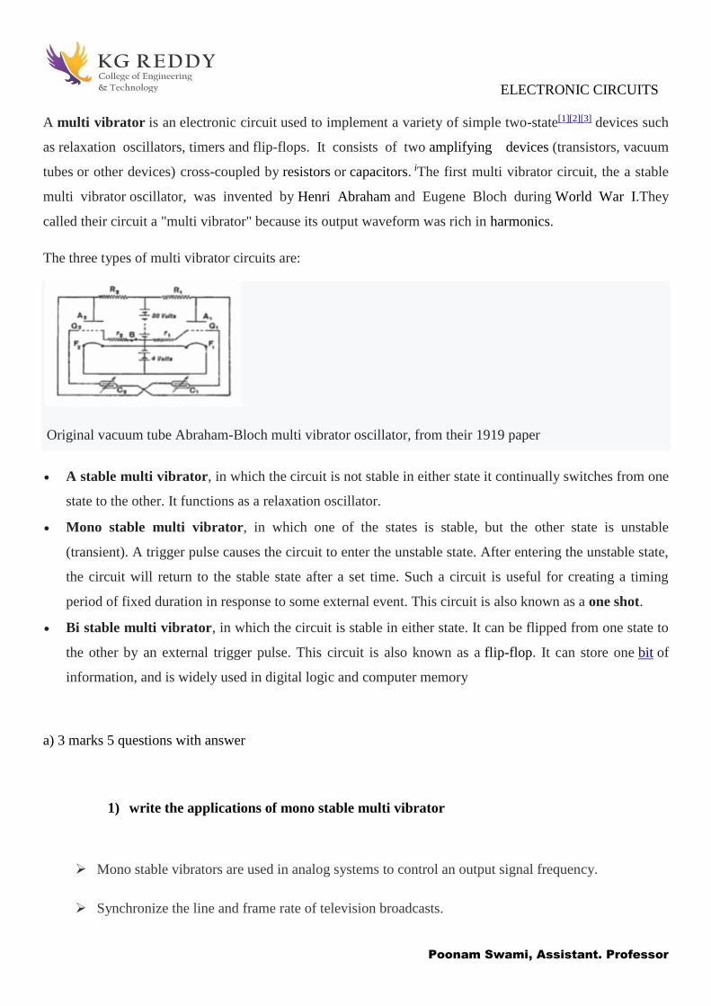
ELECTRONIC CIRCUITS
Poonam Swami, Assistant. Professor
A multi vibrator is an electronic circuit used to implement a variety of simple two-state[1][2][3] devices such
as relaxation oscillators, timers and flip-flops. It consists of two amplifying devices (transistors, vacuum
tubes or other devices) cross-coupled by resistors or capacitors. iThe first multi vibrator circuit, the a stable
multi vibrator oscillator, was invented by Henri Abraham and Eugene Bloch during World War I.They
called their circuit a "multi vibrator" because its output waveform was rich in harmonics.
The three types of multi vibrator circuits are:
Original vacuum tube Abraham-Bloch multi vibrator oscillator, from their 1919 paper
A stable multi vibrator, in which the circuit is not stable in either state it continually switches from one
state to the other. It functions as a relaxation oscillator.
Mono stable multi vibrator, in which one of the states is stable, but the other state is unstable
(transient). A trigger pulse causes the circuit to enter the unstable state. After entering the unstable state,
the circuit will return to the stable state after a set time. Such a circuit is useful for creating a timing
period of fixed duration in response to some external event. This circuit is also known as a one shot.
Bi stable multi vibrator, in which the circuit is stable in either state. It can be flipped from one state to
the other by an external trigger pulse. This circuit is also known as a flip-flop. It can store one bit of
information, and is widely used in digital logic and computer memory
a) 3 marks 5 questions with answer
1) write the applications of mono stable multi vibrator
Mono stable vibrators are used in analog systems to control an output signal frequency.
Synchronize the line and frame rate of television broadcasts.

ELECTRONIC CIRCUITS
Poonam Swami, Assistant. Professor
Even moderate the tunes of different octaves with electronic organs.
Used to hold output voltages in its unstable state for a certain period of time.
2) What are the applications of Schmitt trigger circuit.
1.The Schmitt trigger is a comparator application which switches the output negative when the input
passes upward through a positive reference voltage.
2. It then uses positive feedback of a negative voltage to prevent switching back to the
other state until the input passes through a lower threshold voltage, thus stabilizing the switching
against rapid triggering by noise as it passes the trigger point.
3. That is, it provides feedback which is not reversed in phase, but in this case the signal that is being
fed back is a negative signal and keeps the output driven to the negative supply voltage until the
input drops below the lower design threshold.
3) .Why the mono stable circuit is also called as delay circuit?
Multi vibrators have two different electrical states, an output “HIGH” state and an output “LOW” state
giving them either a stable or quasi-stable state depending upon the type of multi vibrator. One such type
of a two state pulse generator configuration are called Mono stable Multi vibrators.
Mono stable Multi vibrators or “One-Shot Multi vibrators” as they are also called, are used to generate a
single output pulse of a specified width, either “HIGH” or “LOW” when a suitable external trigger signal
or pulse T is applied. This trigger signal initiates a timing cycle which causes the output of the mono
stable to change its state at the start of the timing cycle and will remain in this second state.
4 . what are the other names of bi stable multi vibrator
In the bistable multivibrator, both resistive-capacitive networks (C1-R2 and C2-R3 in Figure 1) are replaced
by resistive networks (just resistors or direct coupling).
This latch circuit is similar to an astable multivibrator, except that there is no charge or discharge time, due
to the absence of capacitors. Hence, when the circuit is switched on, if Q1 is on, its collector is at 0 V. As a

ELECTRONIC CIRCUITS
Poonam Swami, Assistant. Professor
result, Q2 gets switched off. This results in more than half +volts being applied to R4 causing current into
the base of Q1, thus keeping it on. Thus, the circuit remains stable in a single state continuously. Similarly,
Q2 remains on continuously, if it happens to get switched on first.
Switching of state can be done via Set and Reset terminals connected to the bases. For example, if Q2 is on
and Set is grounded momentarily, this switches Q2 off, and makes Q1 on. Thus, Set is used to "set" Q1 on,
and Reset is used to "reset" it to off state.
7.Explain the breakdown voltage consideration of a transistor
Breakdown voltage is a parameter of a diode that defines the largest reverse voltage that can be applied
without causing an exponential increase in the leakage current in the diode. As long as the current is limited,
exceeding the breakdown voltage of a diode does no harm to the diode. In fact, Zener diodes are essentially
just heavily doped normal diodes that exploit the breakdown voltage of a diode to provide regulation of
voltage levels.
Rectifier diodes (semiconductor or tube/valve) may have several voltage ratings, such as the Peak Inverse
Voltage (PIV) across the diode, and the maximum RMS input voltage to the rectifier circuit (which will be
much less).
Many small-signal transistors need to have any breakdown currents limited to much lower values to avoid
excessive heating. To avoid damage to the device, and to limit the effects excessive leakage current may
have on the surrounding circuit, the following bipolar transistor Maximum Ratings are often specified.
VCEO (sometimes written BVCEO or V(BR)CEO – the maximum voltage between collector and emitter that
can be safely applied (and with no more than some specified leakage current, often) when no circuit at
the base of the transistor is there to remove collector-base leakage. Typical values: 20 Volts to as high as
700 Volts; very early Germanium point-contact transistors such as the OC10 had values around 5 Volts
or less.
VCBO – the maximum collector-to-base voltage, with emitter open-circuit. Typical values 25 to 1200
Volts.
VCER – the maximum voltage rating between collector and emitter with some specified resistance (or
less) between base and emitter. A more realistic rating for real-world circuits than the open-base or
open-emitter scenarios above.
VEBO – the maximum reverse voltage on the base with respect to the emitter.
VCES – collector to emitter rating when base is shorted to emitter; equivalent to VCER when R = 0;

ELECTRONIC CIRCUITS
Poonam Swami, Assistant. Professor
Field Effect transistors have similar maximum ratings, the most important one for Junction FETs is the gate-
drain rating .Some devices may also have a maximum rate of change of voltage specified.
a) 5 marks 5 questions with answer
1.Explain the operation of mono stable multi vibrator with waveforms.
Monostable multivibrator has one stable state and one quasi stable state (astable state). When an external
trigger applied to the circuit, the multivibrator will jump to quasi stable state from stable state.
After the period of time it will automatically set back to the stable state, for returning to the stable state
multivibrator does not require any external trigger. The time period to returning to stable state circuit is
always depends on the passive elements in the circuit (resistor and capacitor values
ELECTRONIC CIRCUITS
Poonam Swami, Assistant. Professor
Circuit Operation:
When there is no external trigger to the circuit the one transistor will be in saturation state and other will be
in cutoff state. Q1 is in cutoff mode and put at negative potential until the external trigger to operate, Q2 is
in saturation mode.
Once the external trigger is given to the input Q1 will get turn on and when the Q1 reaches the saturation the
capacitor which is connected to the collector of Q1 and base of Q2 will make transistor Q2 to turn off. This
is state of turn off Q2 transistor is called a stable stable or quasi state.
When capacitor charges to VCC the Q2 will turn on again and automatically Q1 is turn off. So the time
period for charging of capacitor through the resistor is directly proportional to the quasi or a stable state of
multivibrator when a external trigger occurred (t=0.69RC).
Uses of Mono stable Multivibrator:
The mono stable multi vibrators are used as timers, delay circuits, gated circuits etc.
2.With the help of neat waveforms explain the working of A stable multivibrator circuit.
An a stable multivibrator consists of two amplifying stages connected in a positive feedback loop by two
capacitive-resistive coupling networks. The amplifying elements may be junction or field-effect transistors,
vacuum tubes, operational amplifiers, or other types of amplifier. Figure 1, below right, shows bipolar
junction transistors.
The circuit is usually drawn in a symmetric form as a cross-coupled pair. The two output terminals can be
defined at the active devices and have complementary states. One has high voltage while the other has low
voltage, except during the brief transitions from one state to the other.

ELECTRONIC CIRCUITS
Poonam Swami, Assistant. Professor
In the beginning, the capacitor C1 is fully charged (in the previous State 2) to the power supply
voltage V with the polarity shown in Figure 1. Q1 is on and connects the left-hand positive plate of C1 to
ground. As its right-hand negative plate is connected to Q2 base, a maximum negative voltage (-V) is
applied to Q2 base that keeps Q2 firmly off. C1 begins discharging (reverse charging) via the high-value
base resistor R2, so that the voltage of its right-hand plate (and at the base of Q2) is rising from below
ground (-V) toward +V. As Q2 base-emitter junction is reverse-biased, it does not conduct, so all the current
from R2 goes into C1. Simultaneously, C2 that is fully discharged and even slightly charged to 0.6 V (in the
previous State 2) quickly charges via the low-value collector resistor R4 and Q1 forward-biased base-emitter
junction (because R4 is less than R2, C2 charges faster than C1). Thus C2 restores its charge and prepares
for the next State C2 when it will act as a time-setting capacitor. Q1 is firmly saturated in the beginning by
the "forcing" C2 charging current added to R3 current. In the end, only R3 provides the needed input base
current. The resistance R3 is chosen small enough to keep Q1 (not deeply) saturated after C2 is fully
charged.
Figure 1: Basic BJT astable multivibrator
ELECTRONIC CIRCUITS
Poonam Swami, Assistant. Professor
State 1 (Q1 is switched on, Q2 is switched off)
When the voltage of C1 right-hand plate (Q2 base voltage) becomes positive and reaches 0.6 V, Q2 base-
emitter junction begins diverting a part of R2 charging current. Q2 begins conducting and this starts the
avalanche-like positive feedback process as follows. Q2 collector voltage begins falling; this change
transfers through the fully charged C2 to Q1 base and Q1 begins cutting off. Its collector voltage begins
rising; this change transfers back through the almost empty C1 to Q2 base and makes Q2 conduct more thus
sustaining the initial input impact on Q2 base. Thus the initial input change circulates along the feedback
loop and grows in an avalanche-like manner until finally Q1 switches off and Q2 switches on. The forward-
biased Q2 base-emitter junction fixes the voltage of C1 right-hand plate at 0.6 V and does not allow it to
continue rising toward +V.
State 2 (Q1 is switched off, Q2 is switched on)
Now, the capacitor C2 is fully charged (in the previous State 1) to the power supply voltage V with the
polarity shown in Figure 1. Q2 is onand connects the right-hand positive plate of C2 to ground. As its left-
hand negative plate is connected to Q1 base, a maximum negative voltage (-V) is applied to Q1 base that
keeps Q1 firmly off. C2 begins discharging (reverse charging) via the high-value base resistor R3, so that the
voltage of its left-hand plate (and at the base of Q1) is rising from below ground (-V) toward +V.
Simultaneously, C1 that is fully discharged and even slightly charged to 0.6 V (in the previous State 1)
quickly charges via the low-value collector resistor R1 and Q2 forward-biased base-emitter junction
(because R1 is less than R3, C1 charges faster than C2). Thus C1 restores its charge and prepares for the
next State 1 when it will act again as a time-setting capacitor...and so on... (the next explanations are a
mirror copy of the second part of State 1).
3.Draw the circuit of Schmitt trigger and explain its operation .Derive the expression for UTP and
LTP.
a Schmitt trigger is a comparator circuit with hysteresis implemented by applying positive feedback to the
noninverting input of a comparator or differential amplifier. It is an active circuit which converts
an analog input signal to a digital output signal. The circuit is named a "trigger" because the output retains
its value until the input changes sufficiently to trigger a change. In the non-inverting configuration, when the
input is higher than a chosen threshold, the output is high. When the input is below a different (lower)
chosen threshold the output is low, and when the input is between the two levels the output retains its value.
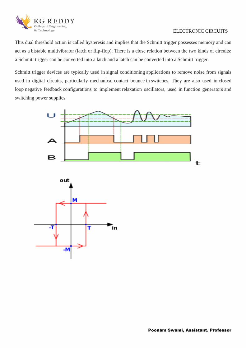
ELECTRONIC CIRCUITS
Poonam Swami, Assistant. Professor
This dual threshold action is called hysteresis and implies that the Schmitt trigger possesses memory and can
act as a bistable multivibrator (latch or flip-flop). There is a close relation between the two kinds of circuits:
a Schmitt trigger can be converted into a latch and a latch can be converted into a Schmitt trigger.
Schmitt trigger devices are typically used in signal conditioning applications to remove noise from signals
used in digital circuits, particularly mechanical contact bounce in switches. They are also used in closed
loop negative feedback configurations to implement relaxation oscillators, used in function generators and
switching power supplies.

ELECTRONIC CIRCUITS
Poonam Swami, Assistant. Professor
4.Explain asymmetrical triggering in a binary mention its uses.
ASYMMETRICAL INVERTING SCHMITT TRIGGER
In previous section we have seen that the triggering points VLT and VUT are having same magnitudes. If
we want to the upper and lower threshold values to be different then an additional battery of potential ‘V’ is
added as shown below.
ASYMMETRICAL INVERTING SCHMITT TRIGGER
In previous section we have seen that the triggering points VLT and VUT are having same magnitudes. If
we want to the upper and lower threshold values to be different then an additional battery of potential ‘V’ is
added as shown below.

ELECTRONIC CIRCUITS
Poonam Swami, Assistant. Professor
To find the triggering points:
Applying KVL at the output side, we get
Vo=IR1+IR2+V
∴I=(Vo-V)/((R1+R2 ) )
From circuit diagram, the threshold (triggering) point can be calculated as
VT=IR2+V
Substituting the equation of ‘I’ in above equation, we get
VT=[(Vo-V)/(R1+R2 )] R2+V
VT=R2/(R1+R2 ) Vo-R2/(R1+R2 ) V+V
VT=R2/(R1+R2 ) Vo+V[1-R2/(R1+R2 )]
VT=R2/(R1+R2 ) Vo+R1/(R1+R2 ) V
When Vout=+Vsat , VT=+ve
When Vout=-Vsat , VT= -veThe input and output waveforms are shown below.The transfer characteristics
are shown below,
5.How does a diode act as switch?
DIODE SWITCH
In addition to their use as simple rectifiers, diodes are also used in circuits that mix signals together
(mixers), detect the presence of a signal (detector), and act as a switch “to open or close a circuit”. Diodes
used in these applications are commonly referred to as “signal diodes”. The simplest application of a signal
diode is the basic diode switch shown in figure 1.
When the input to this circuit is at zero potential, the diode is forward biased because of the zero potential
on the cathode and the positive voltage on the anode. In this condition, the diode conducts and acts as a
straight piece of wire because of its very low forward resistance. In effect, the input is directly coupled to

ELECTRONIC CIRCUITS
Poonam Swami, Assistant. Professor
the output resulting in zero volts across the output terminals. Therefore, the diode, acts as a closed switch
when its anode is positive with respect to its cathode.
If we apply a positive input voltage (equal to or greater than the positive voltage supplied to the anode) to
the diode's cathode, the diode will be reverse biased. In this situation, the diode is cut off and acts as an
open switch between the input and output terminals. Consequently, with no current flow in the circuit, the
positive voltage on the diode's anode will be felt at the output terminal. Therefore, the diode acts as an
open switch when it is reverse biased
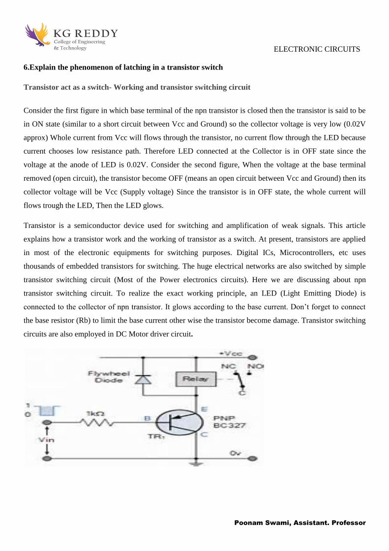
ELECTRONIC CIRCUITS
Poonam Swami, Assistant. Professor
6.Explain the phenomenon of latching in a transistor switch
Transistor act as a switch- Working and transistor switching circuit
Consider the first figure in which base terminal of the npn transistor is closed then the transistor is said to be
in ON state (similar to a short circuit between Vcc and Ground) so the collector voltage is very low (0.02V
approx) Whole current from Vcc will flows through the transistor, no current flow through the LED because
current chooses low resistance path. Therefore LED connected at the Collector is in OFF state since the
voltage at the anode of LED is 0.02V. Consider the second figure, When the voltage at the base terminal
removed (open circuit), the transistor become OFF (means an open circuit between Vcc and Ground) then its
collector voltage will be Vcc (Supply voltage) Since the transistor is in OFF state, the whole current will
flows trough the LED, Then the LED glows.
Transistor is a semiconductor device used for switching and amplification of weak signals. This article
explains how a transistor work and the working of transistor as a switch. At present, transistors are applied
in most of the electronic equipments for switching purposes. Digital ICs, Microcontrollers, etc uses
thousands of embedded transistors for switching. The huge electrical networks are also switched by simple
transistor switching circuit (Most of the Power electronics circuits). Here we are discussing about npn
transistor switching circuit. To realize the exact working principle, an LED (Light Emitting Diode) is
connected to the collector of npn transistor. It glows according to the base current. Don’t forget to connect
the base resistor (Rb) to limit the base current other wise the transistor become damage. Transistor switching
circuits are also employed in DC Motor driver circuit.

ELECTRONIC CIRCUITS
Poonam Swami, Assistant. Professor
PART-A(OBJECTIVE QUESTIONS)
1. A transistor acts as an open switch when it is in [a]
a)cut-off region b)active region
c) saturation region d)none of these
2. A transistor acts as a closed switch when it is in [c]
a) cut-off region b)active region
c) saturation region d)none of these
3. A transistor acts as an amplifier when it is in [b]
a)cut-off region b)active region
c) saturation region d )none of these
4.For a transistor to be in cutoff region, both the junctions of the transistor must be [b] a)forward biased
b)reverse biased c)unbiased d)none
5.In the steady state condition ,the current which flows through the diode is a [a]
a) Diffusion current b) Drift current
c) Reverse current d)none of these
6.Basically how many multi vibrators are there?[a]
a)3 b)4 c)6 d)7
7)Which multi vibrator is called as flip-flop? [a]
a) Bistable b) mono stable
c)Astable d)none
8)In bistable multivibrator,the coupling elements are [b]
a)Both capacitors b)Both resistors

ELECTRONIC CIRCUITS
Poonam Swami, Assistant. Professor
c)one capacitor and resistor d)none
9.In stable state ,the loop gain is [C]
a)>1 b)<1 c)=1 d)=0
10.Which multi vibrator is used as an amplitude comparators [d]
a)Bistable b)monostable
c)Astable d)none
PART-A
1 2 3 4 5 6 7 8 9 10
A C B B A A A B C D
PART-B(FILL IN THE BLANKS)
1 ) The amount of other gates that can be connected to the gate’s output is meant by fan -out of a logic
gate
2) Zener Breakdown occurs below 6V
3) The breakdown which occurs through a direct rupture of bonds because of the existence of the strong
electric field is referred to as Zener breakdown
4. A bistable multivibrator is used for digital operations like couning and storing of binary information.
5.Schmitt trigger can be used to convert a sine wave into a square wave
6.The most important application of a time base generator is in CROs
7. Bistable multi vibrator is used as a memory element.
8.Monostable multivibrator is called as one shot

ELECTRONIC CIRCUITS
Poonam Swami, Assistant. Professor
PART-B
1 The amount of other gates that
can be connected to the gate’s
output is
2 6V
3 Zener breakdown
4 bistable
5 square wave
6 CROs
7 Bi stable
8 one shot
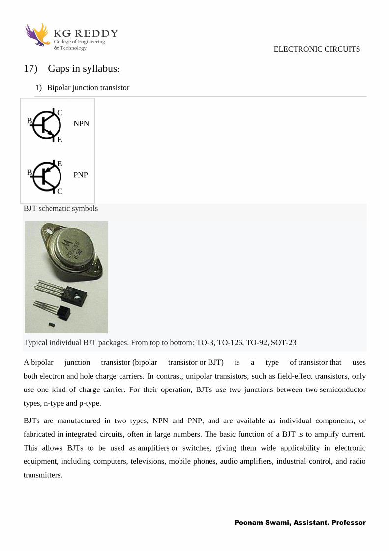
ELECTRONIC CIRCUITS
Poonam Swami, Assistant. Professor
17) Gaps in syllabus:
1) Bipolar junction transistor
NPN
PNP
BJT schematic symbols
Typical individual BJT packages. From top to bottom: TO-3, TO-126, TO-92, SOT-23
A bipolar junction transistor (bipolar transistor or BJT) is a type of transistor that uses
both electron and hole charge carriers. In contrast, unipolar transistors, such as field-effect transistors, only
use one kind of charge carrier. For their operation, BJTs use two junctions between two semiconductor
types, n-type and p-type.
BJTs are manufactured in two types, NPN and PNP, and are available as individual components, or
fabricated in integrated circuits, often in large numbers. The basic function of a BJT is to amplify current.
This allows BJTs to be used as amplifiers or switches, giving them wide applicability in electronic
equipment, including computers, televisions, mobile phones, audio amplifiers, industrial control, and radio
transmitters.
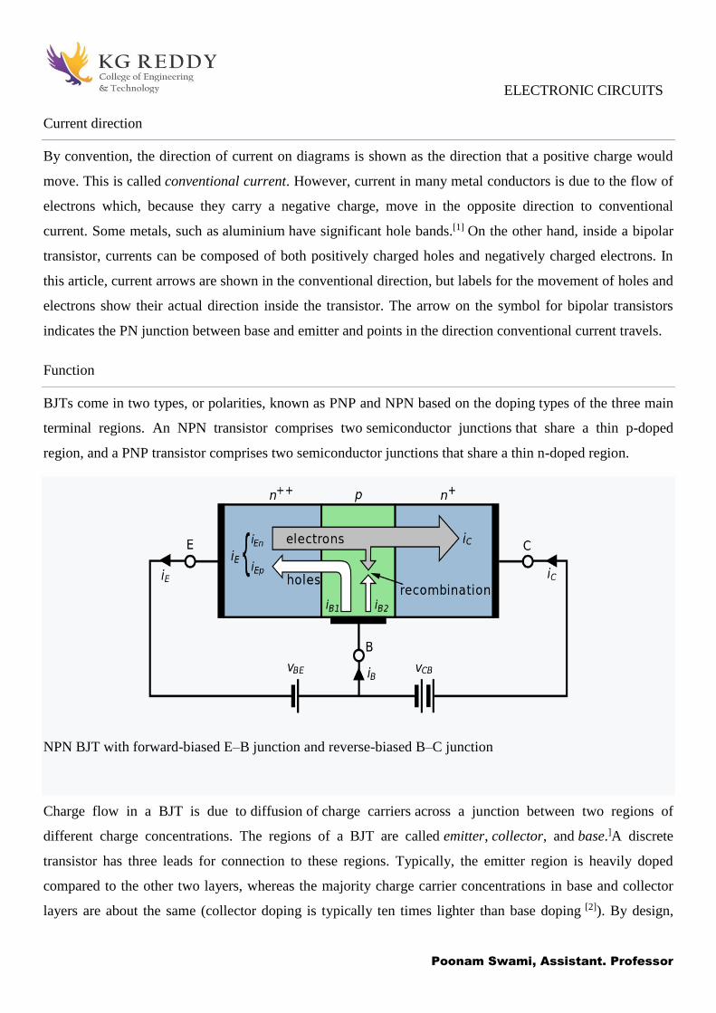
ELECTRONIC CIRCUITS
Poonam Swami, Assistant. Professor
Current direction
By convention, the direction of current on diagrams is shown as the direction that a positive charge would
move. This is called conventional current. However, current in many metal conductors is due to the flow of
electrons which, because they carry a negative charge, move in the opposite direction to conventional
current. Some metals, such as aluminium have significant hole bands.[1] On the other hand, inside a bipolar
transistor, currents can be composed of both positively charged holes and negatively charged electrons. In
this article, current arrows are shown in the conventional direction, but labels for the movement of holes and
electrons show their actual direction inside the transistor. The arrow on the symbol for bipolar transistors
indicates the PN junction between base and emitter and points in the direction conventional current travels.
Function
BJTs come in two types, or polarities, known as PNP and NPN based on the doping types of the three main
terminal regions. An NPN transistor comprises two semiconductor junctions that share a thin p-doped
region, and a PNP transistor comprises two semiconductor junctions that share a thin n-doped region.
NPN BJT with forward-biased E–B junction and reverse-biased B–C junction
Charge flow in a BJT is due to diffusion of charge carriers across a junction between two regions of
different charge concentrations. The regions of a BJT are called emitter, collector, and base.]A discrete
transistor has three leads for connection to these regions. Typically, the emitter region is heavily doped
compared to the other two layers, whereas the majority charge carrier concentrations in base and collector
layers are about the same (collector doping is typically ten times lighter than base doping [2]). By design,
ELECTRONIC CIRCUITS
Poonam Swami, Assistant. Professor
most of the BJT collector current is due to the flow of charge carriers (electrons or holes) injected from a
high-concentration emitter into the base where they are minority carriers that diffuse toward the collector,
and so BJTs are classified as minority-carrier devices.
In typical operation, the base–emitter junction is forward-biased, which means that the p-doped side of the
junction is at a more positive potential than the n-doped side, and the base–collector junction is reverse-
biased. In an NPN transistor, when positive bias is applied to the base–emitter junction, the equilibrium is
disturbed between the thermally generated carriers and the repelling electric field of the n-doped
emitter depletion region. This allows thermally excited electrons to inject from the emitter into the base
region. These electrons diffuse through the base from the region of high concentration near the emitter
towards the region of low concentration near the collector. The electrons in the base are called minority
carriers because the base is doped p-type, which makes holes the majority carrier in the base.
Transistor parameters: alpha (α) and beta (β)
The proportion of electrons able to cross the base and reach the collector is a measure of the BJT efficiency.
The heavy doping of the emitter region and light doping of the base region causes many more electrons to be
injected from the emitter into the base than holes to be injected from the base into the emitter.
The common-emitter current gain is represented by βF or the h-parameter hFE; it is approximately the ratio of
the DC collector current to the DC base current in forward-active region. It is typically greater than 50 for
small-signal transistors, but can be smaller in transistors designed for high-power applications.
Another important parameter is the common-base current gain, αF. The common-base current gain is
approximately the gain of current from emitter to collector in the forward-active region. This ratio usually
has a value close to unity; between 0.980 and 0.998. It is less than unity due to recombination of charge
carriers as they cross the base region.
Alpha and beta are more precisely related by the following identities (NPN transistor):
Structure

ELECTRONIC CIRCUITS
Poonam Swami, Assistant. Professor
Simplified cross section of a planar NPN bipolar junction transistor
A BJT consists of three differently doped semiconductor regions: the emitter region, the base region and
the collector region. These regions are, respectively, p type, n type and p type in a PNP transistor,
and n type, p type and n type in an NPN transistor. Each semiconductor region is connected to a
terminal, appropriately labeled: emitter (E), base (B) and collector (C).
The base is physically located between the emitter and the collector and is made from lightly doped,
high-resistivity material. The collector surrounds the emitter region, making it almost impossible for the
electrons injected into the base region to escape without being collected, thus making the resulting value
of α very close to unity, and so, giving the transistor a large β. A cross-section view of a BJT indicates
that the collector–base junction has a much larger area than the emitter–base junction.
The bipolar junction transistor, unlike other transistors, is usually not a symmetrical device. This means
that interchanging the collector and the emitter makes the transistor leave the forward active mode and
start to operate in reverse mode. Because the transistor's internal structure is usually optimized for
forward-mode operation, interchanging the collector and the emitter makes the values of α and β in
reverse operation much smaller than those in forward operation; often the α of the reverse mode is lower
than 0.5. The lack of symmetry is primarily due to the doping ratios of the emitter and the collector. The
emitter is heavily doped, while the collector is lightly doped, allowing a large reverse bias voltage to be
applied before the collector–base junction breaks down. The collector–base junction is reverse biased in
normal operation. The reason the emitter is heavily doped is to increase the emitter injection efficiency:
the ratio of carriers injected by the emitter to those injected by the base. For high current gain, most of
the carriers injected into the emitter–base junction must come from the emitter.
The low-performance "lateral" bipolar transistors sometimes used in CMOS processes are sometimes
designed symmetrically, that is, with no difference between forward and backward operation.

ELECTRONIC CIRCUITS
Poonam Swami, Assistant. Professor
Small changes in the voltage applied across the base–emitter terminals cause the current between
the emitter and the collector to change significantly. This effect can be used to amplify the input voltage
or current. BJTs can be thought of as voltage-controlled current sources, but are more simply
characterized as current-controlled current sources, or current amplifiers, due to the low impedance at
the base.
Early transistors were made from germanium but most modern BJTs are made from silicon. A
significant minority are also now made from gallium arsenide, especially for very high speed
applications (see HBT, below).
NPN[edit]
The symbol of an NPN BJT. A mnemonic for the symbol is "not pointing in".
NPN is one of the two types of bipolar transistors, consisting of a layer of P-doped semiconductor (the
"base") between two N-doped layers. A small current entering the base is amplified to produce a large
collector and emitter current. That is, when there is a positive potential difference measured from the
base of an NPN transistor to its emitter (that is, when the base is high relative to the emitter), as well as a
positive potential difference measured from the collector to the emitter, the transistor becomes active. In
this "on" state, current flows from the collector to the emitter of the transistor. Most of the current is
carried by electrons moving from emitter to collector as minority carriers in the P-type base region. To
allow for greater current and faster operation, most bipolar transistors used today are NPN
because electron mobility is higher than hole mobility.
A mnemonic device for the NPN transistor symbol is "not pointing in", based on the arrows in the
symbol and the letters in the name.[7]
PNP[edit]
The symbol of a PNP BJT. A mnemonic for the symbol is "points in proudly".

ELECTRONIC CIRCUITS
Poonam Swami, Assistant. Professor
The other type of BJT is the PNP, consisting of a layer of N-doped semiconductor between two layers of
P-doped material. A small current leaving the base is amplified in the collector output. That is, a PNP
transistor is "on" when its base is pulled low relative to the emitter. In a PNP transistor, the emitter–base
region is forward biased, so holes are injected into the base as minority carriers. The base is very thin,
and most of the holes cross the reverse-biased base–collector junction to the collector.
The arrows in the NPN and PNP transistor symbols indicate the PN junction between the base and
emitter. When the device is in forward active or forward saturated mode, the arrow, placed on the
emitter leg, points in the direction of the conventional current.A mnemonic device for the PNP transistor
symbol is "pointing in (proudly/permanently)", based on the arrows in the symbol and the letters in the
name
2) Field-effect transistor
The field-effect transistor (FET) is a transistor that uses an electric field to control the electrical behaviour
of the device. FETs are also known as unipolar transistors since they involve single-carrier-type operation.
Many different implementations of field effect transistors exist. Field effect transistors generally display
very high input impedance at low frequencies. The conductivity between the drain and source terminals is
controlled by an electric field in the device, which is generated by the voltage difference between the body
and the gate of the device.
Basic information
FETs can be majority-charge-carrier devices, in which the current is carried predominantly by majority
carriers, or minority-charge-carrier devices, in which the current is mainly due to a flow of minority
carriers.[3] The device consists of an active channel through which charge carriers, electrons or holes, flow
from the source to the drain. Source and drain terminal conductors are connected to the semiconductor
through ohmic contacts. The conductivity of the channel is a function of the potential applied across the gate
and source terminals.
The FET's three terminals are:[4]
1. Source (S), through which the carriers enter the channel. Conventionally, current entering the
channel at S is designated by IS.
2. Drain (D), through which the carriers leave the channel. Conventionally, current entering the channel
at D is designated by ID. Drain-to-source voltage is VDS.

ELECTRONIC CIRCUITS
Poonam Swami, Assistant. Professor
3. Gate (G), the terminal that modulates the channel conductivity. By applying voltage to G, one can
control ID.
More about terminals
Cross section of an n-type MOSFET
All FETs have source, drain, and gate terminals that correspond roughly to the emitter, collector,
and base of BJTs. Most FETs have a fourth terminal called the body, base, bulk, or substrate. This fourth
terminal serves to bias the transistor into operation; it is rare to make non-trivial use of the body terminal in
circuit designs, but its presence is important when setting up the physical layout of an integrated circuit. The
size of the gate, length L in the diagram, is the distance between source and drain. The width is the extension
of the transistor, in the direction perpendicular to the cross section in the diagram (i.e., into/out of the
screen). Typically the width is much larger than the length of the gate. A gate length of 1 µm limits the
upper frequency to about 5 GHz, 0.2 µm to about 30 GHz.
The names of the terminals refer to their functions. The gate terminal may be thought of as controlling the
opening and closing of a physical gate. This gate permits electrons to flow through or blocks their passage
by creating or eliminating a channel between the source and drain. Electron-flow from the source terminal
towards the drain terminal is influenced by an applied voltage. The body simply refers to the bulk of the
semiconductor in which the gate, source and drain lie. Usually the body terminal is connected to the highest
or lowest voltage within the circuit, depending on the type of the FET. The body terminal and the source
terminal are sometimes connected together since the source is often connected to the highest or lowest
voltage within the circuit, although there are several uses of FETs which do not have such a configuration,
such as transmission gates and cascade circuits.

ELECTRONIC CIRCUITS
Poonam Swami, Assistant. Professor
Effect of gate voltage on current
I–V characteristics and output plot of a JFET n-channel transistor.
Simulation result for right side: formation of inversion channel(electron density) and left side: current-gate
voltage curve(transfer characteristics) in an n-channel nanowire MOSFET. Note that the threshold
voltage for this device lies around 0.45 V.
FET conventional symbol types
ELECTRONIC CIRCUITS
Poonam Swami, Assistant. Professor
The FET controls the flow of electrons (or electron holes) from the source to drain by affecting the size and
shape of a "conductive channel" created and influenced by voltage (or lack of voltage) applied across the
gate and source terminals. (For simplicity, this discussion assumes that the body and source are connected.)
This conductive channel is the "stream" through which electrons flow from source to drain.
N-channel
In an n-channel "depletion-mode" device, a negative gate-to-source voltage causes a depletion region to
expand in width and encroach on the channel from the sides, narrowing the channel. If the active region
expands to completely close the channel, the resistance of the channel from source to drain becomes large,
and the FET is effectively turned off like a switch (see right figure, when there is very small current). This is
called "pinch-off", and the voltage at which it occurs is called the "pinch-off voltage". Conversely, a positive
gate-to-source voltage increases the channel size and allows electrons to flow easily (see right figure, when
there is a conduction channel and current is large).
In an n-channel "enhancement-mode" device, a conductive channel does not exist naturally within the
transistor, and a positive gate-to-source voltage is necessary to create one. The positive voltage attracts free-
floating electrons within the body towards the gate, forming a conductive channel. But first, enough
electrons must be attracted near the gate to counter the doping ions added to the body of the FET; this forms
a region with no mobile carriers called a depletion region, and the voltage at which this occurs is referred to
as the threshold voltage of the FET. Further gate-to-source voltage increase will attract even more electrons
towards the gate which are able to create a conductive channel from source to drain; this process is
called inversion.
P-channel
In a p-channel "depletion-mode" device, a positive voltage from gate to body creates a depletion layer by
forcing the positively charged holes to the gate-insulator/semiconductor interface, leaving exposed a carrier-
free region of immobile, negatively charged acceptor ions. Conversely, in a p-channel "enhancement-mode"
device, a conductive region does not exist and negative voltage must be used to generate a conduction
channel.
Effect of source/drain voltage on channel
For either enhancement- or depletion-mode devices, at drain-to-source voltages much less than gate-to-
source voltages, changing the gate voltage will alter the channel resistance, and drain current will be
proportional to drain voltage (referenced to source voltage). In this mode the FET operates like a variable
resistor and the FET is said to be operating in a linear mode or ohmic mode.

ELECTRONIC CIRCUITS
Poonam Swami, Assistant. Professor
If drain-to-source voltage is increased, this creates a significant asymmetrical change in the shape of the
channel due to a gradient of voltage potential from source to drain. The shape of the inversion region
becomes "pinched-off" near the drain end of the channel. If drain-to-source voltage is increased further, the
pinch-off point of the channel begins to move away from the drain towards the source. The FET is said to be
in saturation mode;[7] although some authors refer to it as active mode, for a better analogy with bipolar
transistor operating regions.[8][9] The saturation mode, or the region between ohmic and saturation, is used
when amplification is needed. The in-between region is sometimes considered to be part of the ohmic or
linear region, even where drain current is not approximately linear with drain voltage.
Even though the conductive channel formed by gate-to-source voltage no longer connects source to drain
during saturation mode, carriers are not blocked from flowing. Considering again an n-channel
enhancement-mode device, a depletion region exists in the p-type body, surrounding the conductive channel
and drain and source regions. The electrons which comprise the channel are free to move out of the channel
through the depletion region if attracted to the drain by drain-to-source voltage. The depletion region is free
of carriers and has a resistance similar to silicon. Any increase of the drain-to-source voltage will increase
the distance from drain to the pinch-off point, increasing the resistance of the depletion region in proportion
to the drain-to-source voltage applied. This proportional change causes the drain-to-source current to remain
relatively fixed, independent of changes to the drain-to-source voltage, quite unlike its ohmic behavior in the
linear mode of operation. Thus, in saturation mode, the FET behaves as a constant-current source rather than
as a resistor, and can effectively be used as a voltage amplifier. In this case, the gate-to-source voltage
determines the level of constant current through the channel.
Advantages
One advantage of the FET is its high gate to main current resistance, on the order of 100 MΩ or more, thus
providing a high degree of isolation between control and flow. Because base current noise will increase with
shaping time,[21] a FET typically produces less noise than a bipolar junction transistor (BJT), and is thus
found in noise sensitive electronics such as tuners and low-noise amplifiers for VHF and satellite receivers.
It is relatively immune to radiation. It exhibits no offset voltage at zero drain current and hence makes an
excellent signal chopper. It typically has better thermal stability than a BJT.[4] Because they are controlled
by gate charge, once the gate is closed or opened, there is no additional power draw, as there would be with
a bipolar junction transistor or with non-latching relays in some states. This allows extremely low-power
switching, which in turn allows greater miniaturization of circuits because heat dissipation needs are reduced
compared to other types of switches.

ELECTRONIC CIRCUITS
Poonam Swami, Assistant. Professor
Disadvantages
It has a relatively low gain–bandwidth product compared to a BJT. The MOSFET has a drawback of being
very susceptible to overload voltages, thus requiring special handling during installation.[22] The fragile
insulating layer of the MOSFET between the gate and channel makes it vulnerable to electrostatic
discharge or changes to threshold voltage during handling. This is not usually a problem after the device has
been installed in a properly designed circuit.
FETs often have a very low "on" resistance and have a high "off" resistance. However, the intermediate
resistances are significant, and so FETs can dissipate large amounts of power while switching. Thus
efficiency can put a premium on switching quickly, but this can cause transients that can excite stray
inductances and generate significant voltages that can couple to the gate and cause unintentional switching.
FET circuits can therefore require very careful layout and can involve trades between switching speed and
power dissipation. There is also a trade-off between voltage rating and "on" resistance, so high-voltage FETs
have a relatively high "on" resistance and hence conduction losses.
3) Two port devices and network parameters.
Models of two-port networks
Many complex, such as amplification circuits and filters, can be modeled by a two-port network model as
shown below. A two-port network is represented by four external variables: voltage and current at
the input port, and voltage and current at the output port, so that the two-port network can be treated
as a black box modeled by the relationships between the four variables , , and . There exist
six different ways to describe the relationships between these variables, depending on which two of the four
variables are given, while the other two can always be derived.

ELECTRONIC CIRCUITS
Poonam Swami, Assistant. Professor
If the network is linear, i.e., each variable can be expressed as a linear function of some two other variables,
then we have the following models:
Z or impedance model: Given two currents and find voltages and by:
Here all four parameters , , , and represent impedance. In
particular, and are transfer impedances, defined as the ratio of a voltage (or ) in
one part of a network to a current (or ) in another part . is a 2 by 2 matrix
containing all four parameters.
Y or admittance model: Given two voltages and , find currents and by:
Here all four parameters , , , and represent admittance. In
particular, and are transfer admittances. is the corresponding parameter matrix.
A or transmission model: Given and , find and by:

ELECTRONIC CIRCUITS
Poonam Swami, Assistant. Professor
Here and are dimensionless coefficients, is impedance and is admittance. A
negative sign is added to the output current in the model, so that the direction of the current is
out-ward, for easy analysis of a cascade of multiple network models.
H or hybrid model: Given and , find and by:
Here and are dimensionless coefficients, is impedance and is admittance.
Generalization to nonlinear circuits
The two-port models can also be applied to a nonlinear circuit if the variations of the variables are small
(small signal models) and therefore the nonlinear behavior of the circuit can be piece-wise linearized.
Assume is a nonlinear function of variables and . If the variations and are
small, the function can be approximated by a linear model
with the linear coefficients
Finding the model parameters

ELECTRONIC CIRCUITS
Poonam Swami, Assistant. Professor
For each of the four types of models, the four parameters can be found from variables ,
, and of a network by the following.
For Z-model:
For Y-model:
For A-model:
For H-model:
If we further define
then the Z-model and Y-model above can be written in matrix form:
Topics beyond syllabus:

ELECTRONIC CIRCUITS
Poonam Swami, Assistant. Professor
1) Analysis of FET:
BIASING OF FET AMPLIFIERS
Fixed Bias
Unlike BJTs, thermal runaway does not occur with FETs. However, the wide differences in maximum and
minimum transfer characteristics make ID levels unpredictable with simple fixed-gate bias voltage. To
obtain reasonable limits on quiescent drain currents ID and drain-source voltage VDS, source resistor and
potential divider bias techniques must be used. With few exceptions, MOSFET bias circuits are similar to
those used for JFETs. Various FET biasing circuits are discussed below:
Fixed Bias:
FIG.: Fixed biasing circuit for JFET
DC bias of a FET device needs setting of gate-source voltage VGS to give desired drain current ID . For a
JFET drain current is limited by the saturation current IDS. Since the FET has such a high input impedance
that no gate current flows and the dc voltage of the gate set by a voltage divider or a fixed battery voltage is
not affected or loaded by the FET.
Fixed dc bias is obtained using a battery VQG. This battery ensures that the gate is always negative with
respect to source and no current flows through resistor RG and gate terminal that is IG =0. The battery
provides a voltage VGS to bias the N-channel JFET, but no resulting current is drawn from the battery
VGG. Resistor RG is included to allow any ac signal applied through capacitor C to develop across RG.
While any ac signal will develop across RG, the dc voltage drop across RG is equal to IG RG = 0 volt.
The gate-source voltage VGS is then VGS = – vG – vs = – vGG – 0 = – VGG.

ELECTRONIC CIRCUITS
Poonam Swami, Assistant. Professor
The drain to source current ID is then fixed by the gate-source voltage as determined by equation. This
current then causes a voltage drop across the drain resistor RD and is given as VRD = ID RD and output
voltage, Vout = VDD – ID RD
Self bias:
FIG.: Self bias circuit for JFET
This is the most common method for biasing a JFET. Self-bias circuit for N-channel JFET is shown in
figure. Since no gate current flows through the reverse-biased gate-source, the gate current IG = 0 and,
therefore,vG = iG RG = 0 With a drain current ID the voltage at the S is, Vs= ID Rs . The gate-source
voltage is then,
VGs = VG – Vs = 0 – ID Rs = – ID Rs. So, voltage drop across resistance Rs provides the biasing voltage
VGg and no external source is required for biasing and this is the reason that it is called self-biasing. The
operating point (that is zero signal ID and VDS) can easily be determined from equation and equation given
below :
VDS = VDD – ID (RD + RS)
Thus dc conditions of JFET amplifier are fully specified. Self biasing of a JFET stabilizes its quiescent
operating point against any change in its parameters like transconductance. Let the given JFET be replaced
by another JFET having the double conductance then drain current will also try to be double but since any
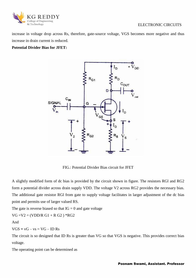
ELECTRONIC CIRCUITS
Poonam Swami, Assistant. Professor
increase in voltage drop across Rs, therefore, gate-source voltage, VGS becomes more negative and thus
increase in drain current is reduced.
Potential Divider Bias for JFET:
FIG.: Potential Divider Bias circuit for JFET
A slightly modified form of dc bias is provided by the circuit shown in figure. The resistors RGl and RG2
form a potential divider across drain supply VDD. The voltage V2 across RG2 provides the necessary bias.
The additional gate resistor RGl from gate to supply voltage facilitates in larger adjustment of the dc bias
point and permits use of larger valued RS.
The gate is reverse biased so that IG = 0 and gate voltage
VG =V2 = (VDD/R G1 + R G2 ) *RG2
And
VGS = vG – vs = VG – ID Rs
The circuit is so designed that ID Rs is greater than VG so that VGS is negative. This provides correct bias
voltage.
The operating point can be determined as
ELECTRONIC CIRCUITS
Poonam Swami, Assistant. Professor
ID = (V2 – VGS)/ RS
And
VDS = VDD – ID (RD + RS)
FET SMALL SIGNAL ANALYSIS
Introduction:
Field-effect transistor amplifiers provide an excellent voltage gain with the added feature of high input
impedance. They are also considered low-power consumption configurations with good frequency range and
minimal size and weight. Both JFET and depletion MOSFET devices can be used to design amplifiers
having similar voltage gains. The depletion MOSFET circuit, however, has much higher input impedance
than a similar JFET configuration.
While a BJT device controls a large output (collector) current by means of a relatively small input (base)
current, the FET device controls an output (drain) current by means of a small input (gate-voltage) voltage.
In general, therefore, the BJT is a current-controlled device and the FET is a voltage-controlled device. In
both cases, however, note that the output current is the controlled variable. Because of the high input
characteristic of FETs, the ac equivalent model is somewhat simpler than that employed for BJTs. While the
BJT had an amplification factor (beta), the FET has a transconductance factor, gm.
The FET can be used as a linear amplifier or as a digital device in logic circuits. In fact, the enhancement
MOSFET is quite popular in digital circuitry, especially in CMOS circuits that require very low power
consumption. FET devices are also widely used in high-frequency applications and in buffering (interfacing)
applications.
While the common-source configuration is the most popular, providing an inverted, amplified signal, one
also finds common-drain (source-follower) circuits providing unity gain with no inversion and common-gate
circuits providing gain with no inversion. As with BJT amplifiers, the important circuit features described in
this chapter include voltage gain, input impedance, and output impedance. Due to the very high input
impedance, the input current is generally assumed to be 0 A and the current gain is an undefined quantity.
While the voltage gain of an FET amplifier is generally less than that obtained using a BJT amplifier, the
FET amplifier provides much higher input impedance than that of a BJT configuration. Output impedance
values are comparable for both BJT and FET circuits.

ELECTRONIC CIRCUITS
Poonam Swami, Assistant. Professor
FIG: small signal model of FET.
COMMON SOURCE AMPLIFIER
A common-source JFET amplifier is one in which the ac input signal is applied to the gate and the ac output
signal is taken from the drain. The source terminal is common to both the input and output signal. A
common-source amplifier either has no source resistor or has a bypassed source resistor, so the source is
connected to ac ground. A self-biased common-source n-channel JFET amplifier with an ac source
capacitively coupled to the gate is shown in Figure below. The resistor, RG, serves two purposes: It keeps
the gate at approximately 0 V dc (because IGSS is extremely small), and its large value (usually several
megohms) prevents loading of the ac signal source. A bias voltage is produced by the drop across RS. The
bypass capacitor, C2, keeps the source of the JFET at ac ground.
FIG.: Self biased Common source Amplifier
The input signal voltage causes the gate-to-source voltage to swing above and below its Q-point value
(VGSQ), causing a corresponding swing in drain current. As the drain current increases, the voltage drop
across RD also increases, causing the drain voltage to decrease. The drain current swings above and below
its Q-point value in phase with the gate-to-source voltage. The drain-to-source voltage swings above and

ELECTRONIC CIRCUITS
Poonam Swami, Assistant. Professor
below its Q-point value (VDSQ) and is 180° out of phase with the gate-to-source voltage, as illustrated in
Figure above. A Graphical Picture The operation just described for an n-channel JFET is illustrated
graphically on both the transfer characteristic curve and the drain characteristic curve in Figure below. Part
(a) shows how a sinusoidal variation, Vgs, produces a corresponding sinusoidal variation in Id. As Vgs
swings from its Q-point value to a more negative value, Id decreases from its Q-point value. As Vgs swings
to a less negative value, Id increases. The signal at the gate drives the drain current above and below the Q-
point on the load line, as indicated by the arrows. Lines projected from the peaks of the gate voltage across
to the ID axis and down to the VDS axis indicate the peak-to-peak variations of the drain current and drain-
to-source voltage, as shown. Because the transfer characteristic curve is nonlinear, the output will have some
distortion. This can be minimized if the signal swings over a limited portion of the load line.
Fig. Transfer Characteristic curve and Drain curve for Common source JFET Amplifier
AC Equivalent Circuit to analyze the signal operation of the amplifier in Figure below ,an ac equivalent
circuit is as follows. Replace the capacitors by effective shorts, based on the simplifying assumption that at
the signal frequency. Replace the dc source by a ground, based on the assumption that the voltage source has
a zero internal resistance. The VDD terminal is at a zero-volt ac potential and therefore acts as an ac ground.
The ac equivalent circuit is shown in Figure below. Notice that the VDD end of Rd and the source terminal
are both effectively at ac ground. Recall that in ac analysis, the ac ground and the actual circuit ground are
treated as the same point.

ELECTRONIC CIRCUITS
Poonam Swami, Assistant. Professor
Fig: The AC equivalent circuit for Common source amplifier
An ac voltage source is shown connected to the input in Figure above. Since the input resistance to a JFET is
extremely high, practically all of the input voltage from the signal source appears at the gate with very little
voltage dropped across the internal source resistance. Vgs = Vin
Voltage Gain The expression for JFET voltage gain that was given in Equation below applies to the
common-source amplifier.
Phase Inversion The output voltage (at the drain) is out of phase with the input voltage (at the gate). The
phase inversion can be designated by a negative voltage gain, Recall that the common-emitter BJT amplifier
also exhibited a phase inversion.
Input Resistance is derived as follows, because the input to a common-source amplifier is at the gate, the
input resistance is extremely high. Ideally, it approaches infinity and can be neglected. As you know, the
high input resistance is produced by the reverse-biased PN junction in a JFET and by the insulated gate
structure in a MOSFET. The actual input resistance seen by the signal source is, the gate-to-ground resistor,
RG, in parallel with the FET’s input resistance, VGS IGSS. The reverse leakage current, IGSS, is typically
given on the datasheet for a specific value of VGS so that the input resistance of the device can be
calculated.
Common drain JFET amplifier
A common-drain JFET amplifier is one in which the input signal is applied to the gate and the output is
taken from the source, making the drain common to both. Because it is common, there is no need for a drain
resistor. A common-drain JFET amplifier is shown in Figure below. A common-drain amplifier is also

ELECTRONIC CIRCUITS
Poonam Swami, Assistant. Professor
called a source-follower. Self-biasing is used in this particular circuit. The input signal is applied to the gate
through a coupling capacitor, C1, and the output signal is coupled to the load resistor through C2.
FIG.: Self biased Common Drain Amplifier
Voltage Gain as in all amplifiers, the voltage gain is Av Vout / Vin. For the source-follower, Vout is IdRs
and Vin is Vgs IdRs as shown in above Figure. Therefore, the gate-to-source voltage gain is IdRs (Vgs
IdRs). Substituting Id gmVgs into the expression gives the following result:
Notice here that the gain is always slightly less than 1. If then a good approximation is Since the output
voltage is at the source, it is in phase with the gate (input) voltage.
Input Resistance because the input signal is applied to the gate, the input resistance seen by the input signal
source is extremely high, just as in the common-source amplifier configuration. The gate resistor, RG, in
parallel with the input resistance looking in at the gate is the total input resistance.
Where
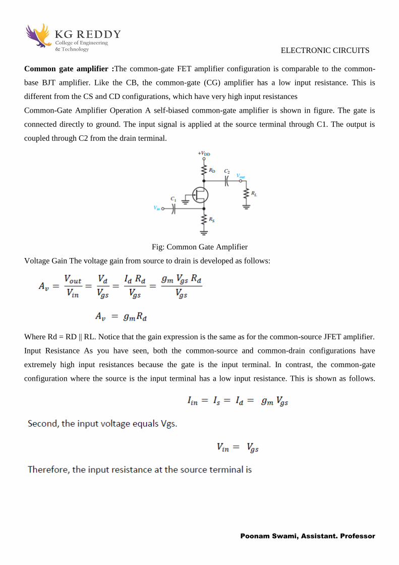
ELECTRONIC CIRCUITS
Poonam Swami, Assistant. Professor
Common gate amplifier :The common-gate FET amplifier configuration is comparable to the common-
base BJT amplifier. Like the CB, the common-gate (CG) amplifier has a low input resistance. This is
different from the CS and CD configurations, which have very high input resistances
Common-Gate Amplifier Operation A self-biased common-gate amplifier is shown in figure. The gate is
connected directly to ground. The input signal is applied at the source terminal through C1. The output is
coupled through C2 from the drain terminal.
Fig: Common Gate Amplifier
Voltage Gain The voltage gain from source to drain is developed as follows:
Where Rd = RD || RL. Notice that the gain expression is the same as for the common-source JFET amplifier.
Input Resistance As you have seen, both the common-source and common-drain configurations have
extremely high input resistances because the gate is the input terminal. In contrast, the common-gate
configuration where the source is the input terminal has a low input resistance. This is shown as follows.
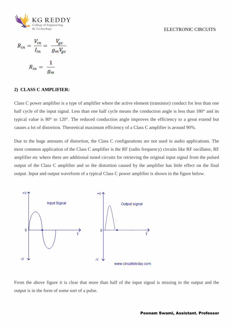
ELECTRONIC CIRCUITS
Poonam Swami, Assistant. Professor
2) CLASS C AMPLIFIER:
Class C power amplifier is a type of amplifier where the active element (transistor) conduct for less than one
half cycle of the input signal. Less than one half cycle means the conduction angle is less than 180° and its
typical value is 80° to 120°. The reduced conduction angle improves the efficiency to a great extend but
causes a lot of distortion. Theoretical maximum efficiency of a Class C amplifier is around 90%.
Due to the huge amounts of distortion, the Class C configurations are not used in audio applications. The
most common application of the Class C amplifier is the RF (radio frequency) circuits like RF oscillator, RF
amplifier etc where there are additional tuned circuits for retrieving the original input signal from the pulsed
output of the Class C amplifier and so the distortion caused by the amplifier has little effect on the final
output. Input and output waveform of a typical Class C power amplifier is shown in the figure below.
From the above figure it is clear that more than half of the input signal is missing in the output and the
output is in the form of some sort of a pulse.

ELECTRONIC CIRCUITS
Poonam Swami, Assistant. Professor
Output characteristics of Class C power amplifier.
In the above figure you can see that the operating point is placed some way below the cut-off point in the
DC load-line and so only a fraction of the input waveform is available at the output.
Class C power amplifier circuit diagram.

ELECTRONIC CIRCUITS
Poonam Swami, Assistant. Professor
Biasing resistor Rb pulls the base of Q1 further downwards and the Q-point will be set some way below the
cut-off point in the DC load line. As a result the transistor will start conducting only after the input signal
amplitude has risen above the base emitter voltage (Vbe~0.7V) plus the downward bias voltage caused by
Rb. That is the reason why the major portion of the input signal is absent in the output signal.
Inductor L1 and capacitor C1 forms a tank circuit which aids in the extraction of the required signal from the
pulsed output of the transistor. Actual job of the active element (transistor) here is to produce a series of
current pulses according to the input and make it flow through the resonant circuit. Values of L1 and C1 are
so selected that the resonant circuit oscillates in the frequency of the input signal. Since the resonant circuit
oscillates in one frequency (generally the carrier frequency) all other frequencies are attenuated and the
required frequency can be squeezed out using a suitably tuned load. Harmonics or noise present in the
output signal can be eliminated using additional filters. A coupling transformer can be used for transferring
the power to the load.
Advantages of Class C power amplifier.
High efficiency.
Excellent in RF applications.
Lowest physical size for a given power output.
Disadvantages of Class C power amplifier.
Lowest linearity.
Not suitable in audio applications.
Creates a lot of RF interference.
It is difficult to obtain ideal inductors and coupling transformers.
Reduced dynamic range.
Applications of Class C power amplifier.
RF oscillators.
RF amplifier.
FM transmitters.
Booster amplifiers.
High frequency repeaters.
Tuned amplifiers etc.

ELECTRONIC CIRCUITS
Poonam Swami, Assistant. Professor