course notes - fermilabepp.fnal.gov/docdb/0002/000227/001/compactfpgadesign.pdf · course notes how...
TRANSCRIPT

Course Notes
How to Design Compact FPGA Functions -- Resource awareness design practices
1 June 2006
Wu, Jinyuan
Wu, Jinyuan Fermilab, MS 222 P.O. Box 500 Batavia, IL 60510 USA E-Mail: [email protected]: (630) 840-8911 FAX: (630) 840-2950

CompactFPGAdesign.doc i 8/15/2006
Table of Contents
1 INTRODUCTION ................................................................................................................................ 4 2 UNDERSTANDING FPGA RESOURCES........................................................................................ 5
2.1 GENERAL PURPOSE RESOURCES ....................................................................................................... 6 2.1.1 Logic Elements ....................................................................................................................... 6 2.1.2 RAM Blocks ............................................................................................................................ 6
2.2 SPECIAL PURPOSE RESOURCES ......................................................................................................... 7 2.2.1 Multipliers .............................................................................................................................. 7 2.2.2 Micro-Processors ................................................................................................................... 7 2.2.3 High Speed Serial Transceivers.............................................................................................. 7
2.3 THE COMPANY OR FAMILY SPECIFIC RESOURCES............................................................................. 7 2.3.1 Distributed RAM and Shift Registers...................................................................................... 7 2.3.2 MUX ....................................................................................................................................... 8 2.3.3 Content Addressable Memory (CAM)..................................................................................... 8
3 SEVERAL PRINCIPLES AND METHODS OF RESOURCE USAGE CONTROL.................... 8 3.1 REUSING SILICON RESOURCES BY PROCESS SEQUENCING ................................................................ 8 3.2 FINDING ALGORITHMS WITH LESS COMPUTATIONS.......................................................................... 9 3.3 USING DEDICATED RESOURCES ........................................................................................................ 9 3.4 MINIMIZING SUPPORTING RESOURCES............................................................................................ 10 3.5 REMAIN CONTROL ON THE COMPLIERS........................................................................................... 10 3.6 USING GOOD LIBRARIES ................................................................................................................. 11
4 SEVERAL EXAMPLES FOR FRONT END ELECTRONICS..................................................... 11 4.1 TDC IN FPGA................................................................................................................................. 11 4.2 ZERO-SUPPRESSION AND TIME STAMP ASSIGNMENT...................................................................... 12 4.3 PIPELINE VS. FIFO .......................................................................................................................... 13 4.4 CLOCK-COMMAND COMBINED CARRIER CODING (C5) .................................................................. 15 4.5 PARASITIC EVENT BUILDING .......................................................................................................... 16 4.6 DIGITAL PHASE FOLLOWER ............................................................................................................ 17 4.7 MULTI-CHANNEL DE-SERIALIZATION ............................................................................................. 19
5 SEVERAL EXAMPLES FOR DAILY DESIGN JOBS.................................................................. 21 5.1 TEMPERATURE DIGITIZATION OF TMP03/04 DEVICES ................................................................... 21 5.2 SILICON SERIAL NUMBER (DS2401) READOUT .............................................................................. 22
6 SEVERAL EXAMPLES FOR ADVANCED TRIGGER SYSTEMS............................................ 23 6.1 TRIGGER PRIMITIVE CREATION....................................................................................................... 23 6.2 UNROLLING NESTED-LOOPS, DOUBLET FINDING............................................................................ 24
6.2.1 Functional Block Arrays....................................................................................................... 25 6.2.2 Contents Addressable Memory (CAM) ................................................................................. 27 6.2.3 Hash Sorter........................................................................................................................... 27
6.3 UNROLLING NESTED-LOOPS, TRIPLET FINDING.............................................................................. 28 6.3.1 The Hough Transform .......................................................................................................... 29 6.3.2 The Tiny Triplet Finder (TTF) .............................................................................................. 30
6.4 TRACK FITTER ................................................................................................................................ 30 7 SEVERAL EXAMPLES FOR FPGA COMPUTATION ............................................................... 32
7.1 SLIDING SUM, PEDESTAL AND RMS ............................................................................................... 32 7.2 CENTER OF GRAVITY METHOD OF PULSE TIME CALCULATION ...................................................... 33 7.3 LOOKUP TABLE USAGE................................................................................................................... 34 7.4 THE ENCLOSED LOOP MICRO-SEQUENCER (ELMS) ....................................................................... 34

CompactFPGAdesign.doc ii 8/15/2006
Index of Figures Figure 1.1 FPGA Price of Several Device Families (June, 2006) .................................................................. 4 Figure 2.1 Cyclone II Logic Element, Left: Normal Mode, Right: Arithmetic Mode (Taken from the Data
Book, to get permit)................................................................................................................................ 6 Figure 3.1 An Example of Process Sequencing.............................................................................................. 8 Figure 3.2 An Example for Minimizing Supporting Resources ................................................................... 10 Figure 4.1 TDC structures in FPGA............................................................................................................. 11 Figure 4.2 Zero-Suppression for Non-Trigger Front End............................................................................. 12 Figure 4.3 Data Output Rate from the FPGA ............................................................................................... 13 Figure 4.4 Pipeline and FIFO Buffers .......................................................................................................... 13 Figure 4.5 A Trigger Front-End ................................................................................................................... 14 Figure 4.6 Implementation of Pipeline Using FIFO ..................................................................................... 15 Figure 4.7 The C5 Pulse Trains .................................................................................................................... 16 Figure 4.8 Data Output Rate from the FPGA ............................................................................................... 16 Figure 4.9 The Parasitic Event Building in an FPGA................................................................................... 17 Figure 4.10 The Multi-sampling and Digital Phase Follower ...................................................................... 18 Figure 4.11 The Transition Detection in the Digital Phase Follower ........................................................... 18 Figure 4.12 The Digital Phase Following Processes .................................................................................... 19 Figure 4.13 The Multi-channel De-serialization Schemes ........................................................................... 20 Figure 4.14 The Delay-Shift-Delay Multi-channel De-serialization Scheme............................................... 20 Figure 5.1 The Temperature Digitization Circuit ......................................................................................... 21 Figure 5.2 The Silicon Serial Number Readout Circuit................................................................................ 22 Figure 6.1 Time-of Flight (TOF) Detector and Trigger Primitives .............................................................. 23 Figure 6.2 The Time-of Flight (TOF) as Function of Hit Position ............................................................... 24 Figure 6.3 A Hit Pairing Problem................................................................................................................. 25 Figure 6.4 A Functional Block Array for Range Cutting ............................................................................. 26 Figure 6.5 A Functional Block Array of Multi-Equality .............................................................................. 26 Figure 6.6 The Contents Addressable Memory as a Single Equality Functional Block Array..................... 27 Figure 6.7 The Hash Sorter .......................................................................................................................... 27 Figure 6.8 Examples of Triplet Finding ....................................................................................................... 28 Figure 6.9 Hough Transform for Triplet Finding ......................................................................................... 29 Figure 6.10 The Tiny Triplet Finder............................................................................................................. 30 Figure 6.11 The Curved Track Fitting.......................................................................................................... 31 Figure 7.1 Sliding Sum, Pedestal and RMS Calculations............................................................................. 32 Figure 7.2 The Simulated Pulse with Noise ................................................................................................. 33 Figure 7.3 Center of Gravity Method for Pulse Time Estimate.................................................................... 34 Figure 7.4 The Micro-Sequencers ................................................................................................................ 35
Index of Tables Table 1-1 Number of Transistors Needed for Various Functions................................................................... 5 Table 6-1 The Coefficients of the FPGA Fitting Algorithm......................................................................... 31

CompactFPGAdesign.doc iii 8/15/2006
Document Revision History Revision Number
Date Description
1 June 1, 2006 Original version
1.1 July 24, 2006 First Draft done.

1 Introduction FPGA application has been very popular in high-energy/nuclear physics experiment apparatus. The functionalities of the FPGA devices range from merely glue logic to full data acquisition and processing.
Like any computing options, FPGA computing also consumes resources. The direct resource consumption is essentially in terms of silicon area that translates to cost of the FPGA devices. As a result of direct silicon resource consumption, indirect cost must also be paid in terms of FPGA recompile time, printed circuit board complexity, power usage, cooling issues etc.
Sometimes, we hear saying that FPGA is cheap. Actual prices of several FPGA device families taken from website of a distributor (Digikey, June 1, 2006) are plotted in Figure 1.1. Each device may have various speed grades and packages that change the price in a large range. The lowest price for each device is chosen for our plots.
0
500
1000
1500
2000
2500
0 20,000 40,000 60,000 80,000 100,000
Number of Logic Cells
Pric
e(U
S$)
XC3SCycloneIIV2PStratix II
0
5
10
15
20
25
30
35
0 20,000 40,000 60,000 80,000 100,000
Number of Logic Cells
Pric
e/(1
000
Logi
cCe
lls)(
US$
)
XC3SCycloneIIV2PStratix II
Figure 1.1
FPGA Price of Several Device Families (June, 2006)
It can be seen that FPGA devices are not so cheap. In terms of absolute pricing, there are devices below $100 and there are also devices more than $1000. While compared within a family, lower middle size devices have lowest price per logic cell.
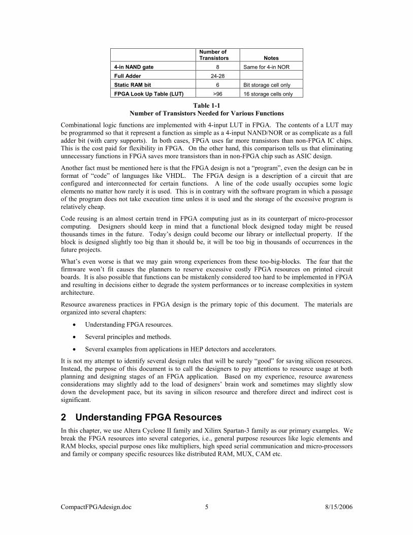
The FPGA cost can be studied by comparing number of transistors needed to implement certain functions in FPGA and non-FPGA IC chips, such as in micro-processors. Several commonly used digital processing functions are compared in Table 1-1.
CompactFPGAdesign.doc 5 8/15/2006
Number of Transistors Notes
4-in NAND gate 8 Same for 4-in NOR Full Adder 24-28 Static RAM bit 6 Bit storage cell only FPGA Look Up Table (LUT) >96 16 storage cells only
Table 1-1 Number of Transistors Needed for Various Functions
Combinational logic functions are implemented with 4-input LUT in FPGA. The contents of a LUT may be programmed so that it represent a function as simple as a 4-input NAND/NOR or as complicate as a full adder bit (with carry supports). In both cases, FPGA uses far more transistors than non-FPGA IC chips. This is the cost paid for flexibility in FPGA. On the other hand, this comparison tells us that eliminating unnecessary functions in FPGA saves more transistors than in non-FPGA chip such as ASIC design.
Another fact must be mentioned here is that the FPGA design is not a “program”, even the design can be in format of “code” of languages like VHDL. The FPGA design is a description of a circuit that are configured and interconnected for certain functions. A line of the code usually occupies some logic elements no matter how rarely it is used. This is in contrary with the software program in which a passage of the program does not take execution time unless it is used and the storage of the excessive program is relatively cheap.
Code reusing is an almost certain trend in FPGA computing just as in its counterpart of micro-processor computing. Designers should keep in mind that a functional block designed today might be reused thousands times in the future. Today’s design could become our library or intellectual property. If the block is designed slightly too big than it should be, it will be too big in thousands of occurrences in the future projects.
What’s even worse is that we may gain wrong experiences from these too-big-blocks. The fear that the firmware won’t fit causes the planners to reserve excessive costly FPGA resources on printed circuit boards. It is also possible that functions can be mistakenly considered too hard to be implemented in FPGA and resulting in decisions either to degrade the system performances or to increase complexities in system architecture.
Resource awareness practices in FPGA design is the primary topic of this document. The materials are organized into several chapters:
• Understanding FPGA resources.
• Several principles and methods.
• Several examples from applications in HEP detectors and accelerators.
It is not my attempt to identify several design rules that will be surely “good” for saving silicon resources. Instead, the purpose of this document is to call the designers to pay attentions to resource usage at both planning and designing stages of an FPGA application. Based on my experience, resource awareness considerations may slightly add to the load of designers’ brain work and sometimes may slightly slow down the development pace, but its saving in silicon resource and therefore direct and indirect cost is significant.
2 Understanding FPGA Resources In this chapter, we use Altera Cyclone II family and Xilinx Spartan-3 family as our primary examples. We break the FPGA resources into several categories, i.e., general purpose resources like logic elements and RAM blocks, special purpose ones like multipliers, high speed serial communication and micro-processors and family or company specific resources like distributed RAM, MUX, CAM etc.

CompactFPGAdesign.doc 6 8/15/2006
2.1 General Purpose Resources Nearly all main stream FPGA devices contain logic elements (logic cells) and memory blocks.
2.1.1 Logic Elements
The logic elements (LE) are the essential building blocks in FPGA devices. A logic element normally consists of a 4-input look up table (LUT) for combinational logic and a flip-flop (FF) for sequential operation. The Cyclone II logic element is shown in Figure 2.1.
Figure 2.1 Cyclone II Logic Element, Left: Normal Mode, Right: Arithmetic Mode (Taken from the Data Book,
to get permit)
Typically, logic elements are organized in arrays and chained interconnections are provided. Perhaps the most common chain support is the carry chain that allows the LE to be used as a bit in an adder or a counter.
The LUT itself is a small 16x1-bit RAM with contents pre-loaded at the configuration stage. Clearly any combinational logic with 4 input signals can be implemented which is the primary reason of flexibility of FPGA devices. But when there are more than 4 signals to participate the logic function, more layers of LUT are normally necessary. For example, if we need a 7-input AND gate, it can be implemented with two cascaded look up tables.
The output of the combinational signals is often registered by the FF to implement sequential functions such as accumulator, counter or any pipelined processing stage.
The FF in the logic element can be bypassed so that the combinational output is sent out directly to other logic elements to form logic functions that need more than 4 inputs. In this case, the FF itself can be used as “packed register”, i.e., a register without the LUT.
Just as in any digital circuit design, for a given logic function, the more pipeline stages, the less combinational propagation delay between the registers of the stages, the faster the system clock can operate. Unlike in ASIC, adding pipeline stages in FPGA normally won’t increase logic element usage too much, since the FF exists already in each logic element. In practice, however, the number of pipeline stages or the maximum operating frequency is not designed to the maximum, but rather to a value with balanced considerations in various aspects.
The logic elements are typically designed to support carry chain so that a full adder can be implemented with one logic element (otherwise it needs two). Counters and accumulators are implemented with a full adder feeding a register.
2.1.2 RAM Blocks
RAM blocks are provided in nearly all FPGA devices. In most families, the address, data and control ports of RAM blocks are registered for synchronous operation so that the RAM blocks can run at higher speed. It is very common that the RAM blocks provided in FPGA are true dual-port RAM blocks.
If a RAM block is pre-loaded with initial contents and not be overwritten by the users, it becomes a ROM. It is more economical to implement ROM using RAM block if relatively large amount of words are to be stored. To implement ROM with less than 16 words, use LUT.

CompactFPGAdesign.doc 7 8/15/2006
The input and output data ports can have different widths. This feature allows the user to buffer parallel data and send out data serially or to store data from a serial port and readout entire word later.
2.2 Special Purpose Resources In principle, almost all digital logic circuits can be built with logic elements. However, as pointed earlier, logic elements use more transistors to implement logic functions, which is a trade off of flexibility. In FPGA devices, certain special purpose resources are provided so that functions can be implemented with reasonable amount of resources. In timing domain, specially designed high speed serial transceivers are provided in some FPGA families for fast communications.
2.2.1 Multipliers
Multipliers become popular in today’s FPGA families. Typical multipliers use O(N2) full adders where N is number of bits of the two operands, which would use too many transistors and consume too much power if implemented with logic cells. Therefore, it is recommended to use dedicated multipliers rather than building them from logic cells when the multiplication operations are needed.
However, multiplications are resource and power consuming operations intrinsically. If multiplications can be eliminated, reduced or replaced, it is recommended to do so.
2.2.2 Micro-Processors
The PowerPC blocks are found in Xilinx Virtex-II Pro family. Generally speaking, dedicated micro-processor blocks use less transistors comparing implementing the processors with soft cores that use logic elements.
Using micro-processors, either dedicated blocks or soft cores needs to be carefully considered in planning stage since it is a relatively large investment.
2.2.3 High Speed Serial Transceivers
High speed serial transceivers are found in both Altera and Xilinx FPGA families. These transceivers operate at multi- Gb/s data rate and popular encoding schemes like 8B/10B and 64B/66B are usually supported. The usefulness of the high speed serial data links is obvious.
The only reminder for the designers is that the data rate of multi- Gb/s is too high for many typical data communication links in daily projects. If in a project, 500 Mb/s or lower data rate is sufficient, it is not recommended to get the “free” “safety factor” to go multi- Gb/s. In addition to the device cost and power consumption, the connectors and cables for multi- Gb/s links require more careful selection and design, while for low rate links, low cost twist pair cables usually work well.
2.3 The Company or Family Specific Resources Several useful resources can be found in certain FPGA families.
2.3.1 Distributed RAM and Shift Registers
The LUTs in FPGA are typically 16x1-bit RAMs. However, the LUTs are normally written in FPGA configuration stage and the contents can not be modified by user during the operating stage. In several families of Xilinx FPGA, the LUT can be configured as RAM or shift register so that the user can use it to store information. Please read the application notes [XAPP464] and [XAP465] for detail.
The distributed RAMs can be used to implement register files. In this case, a logic element stores 16 bits data rather than 1 bit in typical implementation.
With the user-writeable support, the applications of the distributed RAM and shift register are far broader than just storing information. An example of the distributed RAM application can be found in our paper [TTF_paper05_vMar06.pdf]. Another example given in the application note [XAPP194] shows the application of the shift register.
CompactFPGAdesign.doc 8 8/15/2006
2.3.2 MUX
In some families of Xilinx FPGA, dedicated multiplexers are designed in addition to the regular combinational LUT logic. A 2:1 multiplexer can certainly be implemented with a regular LUT using 3 inputs, but a dedicated MUX uses a lot less transistors.
When a relatively wide MUX is needed, using dedicated MUX in Xilinx FPGA saves resource comparing purely using LUT. The application note [XAPP466] is a good source on this topic.
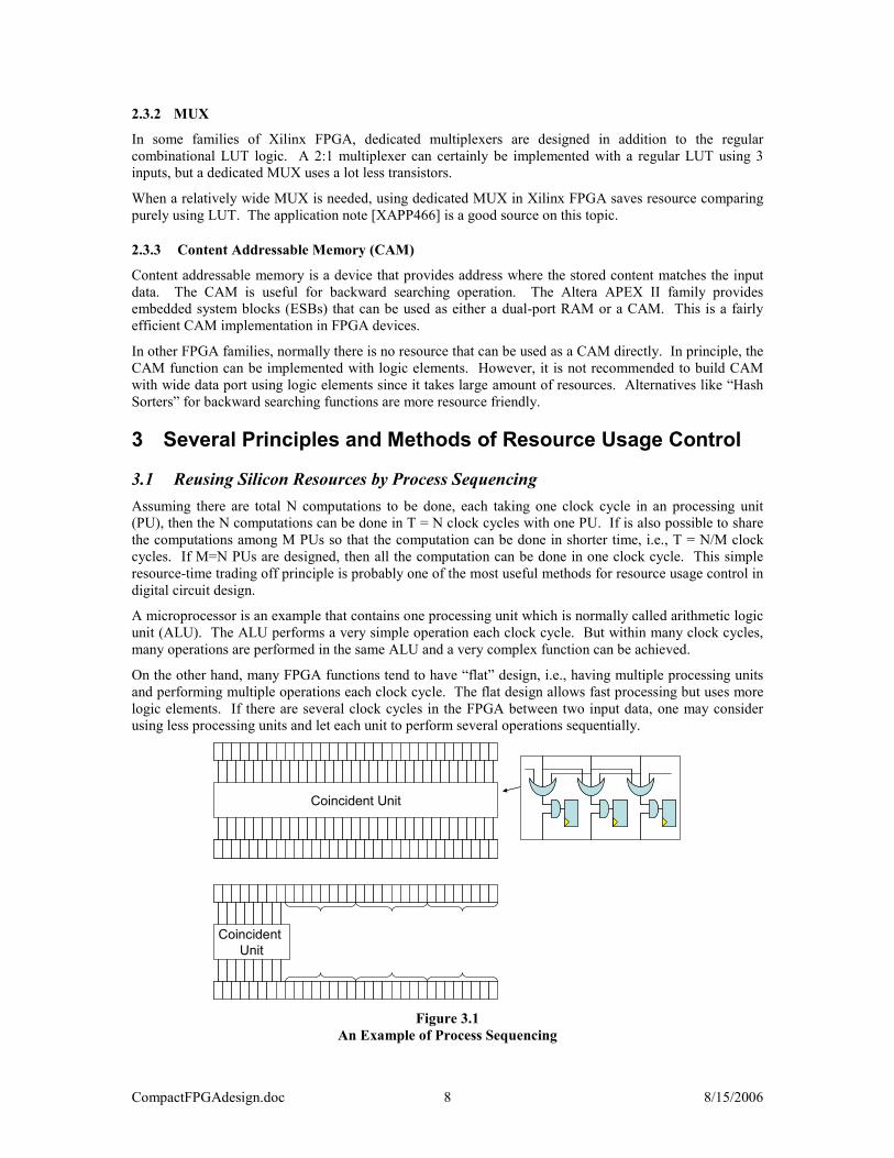
2.3.3 Content Addressable Memory (CAM)
Content addressable memory is a device that provides address where the stored content matches the input data. The CAM is useful for backward searching operation. The Altera APEX II family provides embedded system blocks (ESBs) that can be used as either a dual-port RAM or a CAM. This is a fairly efficient CAM implementation in FPGA devices.
In other FPGA families, normally there is no resource that can be used as a CAM directly. In principle, the CAM function can be implemented with logic elements. However, it is not recommended to build CAM with wide data port using logic elements since it takes large amount of resources. Alternatives like “Hash Sorters” for backward searching functions are more resource friendly.
3 Several Principles and Methods of Resource Usage Control
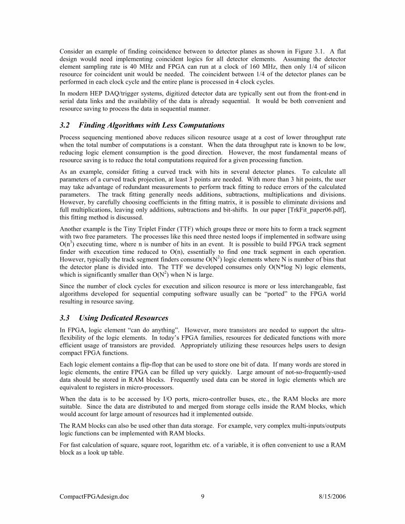
3.1 Reusing Silicon Resources by Process Sequencing Assuming there are total N computations to be done, each taking one clock cycle in an processing unit (PU), then the N computations can be done in T = N clock cycles with one PU. If is also possible to share the computations among M PUs so that the computation can be done in shorter time, i.e., T = N/M clock cycles. If M=N PUs are designed, then all the computation can be done in one clock cycle. This simple resource-time trading off principle is probably one of the most useful methods for resource usage control in digital circuit design.
A microprocessor is an example that contains one processing unit which is normally called arithmetic logic unit (ALU). The ALU performs a very simple operation each clock cycle. But within many clock cycles, many operations are performed in the same ALU and a very complex function can be achieved.
On the other hand, many FPGA functions tend to have “flat” design, i.e., having multiple processing units and performing multiple operations each clock cycle. The flat design allows fast processing but uses more logic elements. If there are several clock cycles in the FPGA between two input data, one may consider using less processing units and let each unit to perform several operations sequentially.
Coincident Unit
Coincident Unit
Figure 3.1 An Example of Process Sequencing
CompactFPGAdesign.doc 9 8/15/2006
Consider an example of finding coincidence between to detector planes as shown in Figure 3.1. A flat design would need implementing coincident logics for all detector elements. Assuming the detector element sampling rate is 40 MHz and FPGA can run at a clock of 160 MHz, then only 1/4 of silicon resource for coincident unit would be needed. The coincident between 1/4 of the detector planes can be performed in each clock cycle and the entire plane is processed in 4 clock cycles.
In modern HEP DAQ/trigger systems, digitized detector data are typically sent out from the front-end in serial data links and the availability of the data is already sequential. It would be both convenient and resource saving to process the data in sequential manner.
3.2 Finding Algorithms with Less Computations Process sequencing mentioned above reduces silicon resource usage at a cost of lower throughput rate when the total number of computations is a constant. When the data throughput rate is known to be low, reducing logic element consumption is the good direction. However, the most fundamental means of resource saving is to reduce the total computations required for a given processing function.
As an example, consider fitting a curved track with hits in several detector planes. To calculate all parameters of a curved track projection, at least 3 points are needed. With more than 3 hit points, the user may take advantage of redundant measurements to perform track fitting to reduce errors of the calculated parameters. The track fitting generally needs additions, subtractions, multiplications and divisions. However, by carefully choosing coefficients in the fitting matrix, it is possible to eliminate divisions and full multiplications, leaving only additions, subtractions and bit-shifts. In our paper [TrkFit_paper06.pdf], this fitting method is discussed.
Another example is the Tiny Triplet Finder (TTF) which groups three or more hits to form a track segment with two free parameters. The processes like this need three nested loops if implemented in software using O(n3) executing time, where n is number of hits in an event. It is possible to build FPGA track segment finder with execution time reduced to O(n), essentially to find one track segment in each operation. However, typically the track segment finders consume O(N2) logic elements where N is number of bins that the detector plane is divided into. The TTF we developed consumes only O(N*log N) logic elements, which is significantly smaller than O(N2) when N is large.
Since the number of clock cycles for execution and silicon resource is more or less interchangeable, fast algorithms developed for sequential computing software usually can be “ported” to the FPGA world resulting in resource saving.
3.3 Using Dedicated Resources In FPGA, logic element “can do anything”. However, more transistors are needed to support the ultra-flexibility of the logic elements. In today’s FPGA families, resources for dedicated functions with more efficient usage of transistors are provided. Appropriately utilizing these resources helps users to design compact FPGA functions.
Each logic element contains a flip-flop that can be used to store one bit of data. If many words are stored in logic elements, the entire FPGA can be filled up very quickly. Large amount of not-so-frequently-used data should be stored in RAM blocks. Frequently used data can be stored in logic elements which are equivalent to registers in micro-processors.
When the data is to be accessed by I/O ports, micro-controller buses, etc., the RAM blocks are more suitable. Since the data are distributed to and merged from storage cells inside the RAM blocks, which would account for large amount of resources had it implemented outside.
The RAM blocks can also be used other than data storage. For example, very complex multi-inputs/outputs logic functions can be implemented with RAM blocks.
For fast calculation of square, square root, logarithm etc. of a variable, it is often convenient to use a RAM block as a look up table.
CompactFPGAdesign.doc 10 8/15/2006
The RAM blocks in many FPGA families are dual-port and the users are allowed to specify different data width for the two ports. Sometimes, the data width of a port is specified to be 1-bit that allows the user to make a handy serial-to-parallel or parallel-to-serial conversions.
As mentioned earlier, a CMOS full adder uses 24-28 transistors while an LE in FPGA takes more than 96 transistors. To implement functions like counters or accumulators using LE, the inefficiency problem of transistor usage is not very serious. For example, a 32-bit accumulator uses 33-35 logic elements which are relatively small fraction of typical FPGA devices. To implement a 32-bit multiplier, on the other hand, at least 512 full adders are needed which become a concern in applications when many multiplications are anticipated. Therefore, many today’s FPGA families provide multipliers.
Generally speaking, when a multiplication is absolutely needed, use a dedicated multiplier rather than implementing the multiplier with logic elements.
However, there are a finite number of multipliers in a given FPGA device. Multiplication is intrinsically a power consuming operation, despite relatively efficient transistor usage in dedicated multipliers. Avoiding multiplication or substituting it with other operations like shifting and addition is still a good practice.
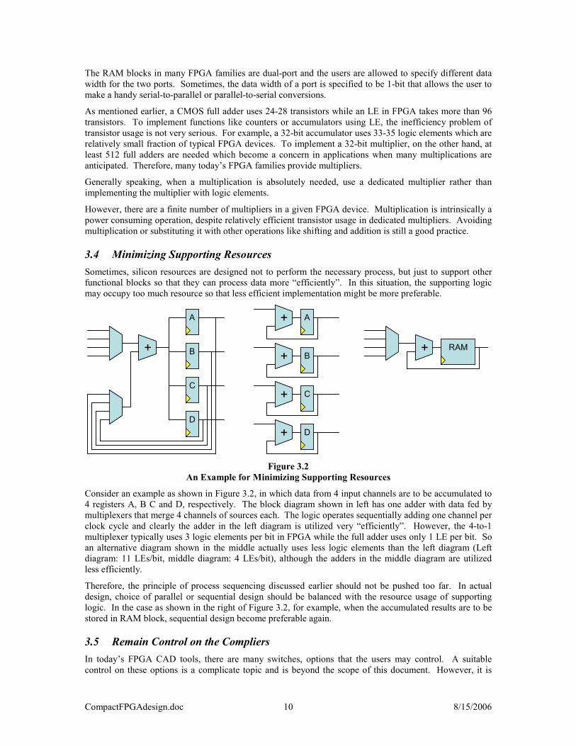
3.4 Minimizing Supporting Resources Sometimes, silicon resources are designed not to perform the necessary process, but just to support other functional blocks so that they can process data more “efficiently”. In this situation, the supporting logic may occupy too much resource so that less efficient implementation might be more preferable.
A
B
C
D
A
B
C
D
+
++
++
RAM+
A
B
C
D
A
B
C
D
+
++
++
RAM+
Figure 3.2 An Example for Minimizing Supporting Resources
Consider an example as shown in Figure 3.2, in which data from 4 input channels are to be accumulated to 4 registers A, B C and D, respectively. The block diagram shown in left has one adder with data fed by multiplexers that merge 4 channels of sources each. The logic operates sequentially adding one channel per clock cycle and clearly the adder in the left diagram is utilized very “efficiently”. However, the 4-to-1 multiplexer typically uses 3 logic elements per bit in FPGA while the full adder uses only 1 LE per bit. So an alternative diagram shown in the middle actually uses less logic elements than the left diagram (Left diagram: 11 LEs/bit, middle diagram: 4 LEs/bit), although the adders in the middle diagram are utilized less efficiently.
Therefore, the principle of process sequencing discussed earlier should not be pushed too far. In actual design, choice of parallel or sequential design should be balanced with the resource usage of supporting logic. In the case as shown in the right of Figure 3.2, for example, when the accumulated results are to be stored in RAM block, sequential design become preferable again.
3.5 Remain Control on the Compliers In today’s FPGA CAD tools, there are many switches, options that the users may control. A suitable control on these options is a complicate topic and is beyond the scope of this document. However, it is

CompactFPGAdesign.doc 11 8/15/2006
recommended that the designers to frequently read the compilation reports to monitor the compiler operation and the outcomes.
Among many items being reported, perhaps the resource usage and maximum operating frequency of the compiled project are the most interesting ones. When the resource usage is unusually bigger than hand estimate, poor design or compiler options can be traced. Excessive resource usage sometime is coupled with drop of maximum operating frequency.
3.6 Using Good Libraries There are intellectual property (IP) cores or other reusable codes available for FPGA designers. The quality of them varies in a very big range. Before blending them into the users’ projects, it is recommended to evaluate them in a test project. Comparing resource usages of the compiled result and the hand estimate gives various hints on the internal implementation and helps the designers to understand the library items better.
4 Several Examples for Front End Electronics
4.1 TDC in FPGA Many time measurement functions in high-energy/nuclear physics experiments can be implemented in FPGA directly. There are two types of practical TDC structures one may choose from as shown in Figure 4.1.
IN
CLK
N2-
N1=
(1/f)
/∆t
c0
c90
c180
c270
c0
Data In
MultipleSampling
ClockDomain
Changing
Trans. Detection& Encode
Q0
Q1
Q2
Q3QF
QE
QD
c90
Coarse TimeCounter
DVT0T1
TS
IN
CLK
N2-
N1=
(1/f)
/∆t
IN
CLK
N2-
N1=
(1/f)
/∆t
c0
c90
c180
c270
c0
Data In
MultipleSampling
ClockDomain
Changing
Trans. Detection& Encode
Q0
Q1
Q2
Q3QF
QE
QD
c90
Coarse TimeCounter
DVT0T1
TS
c0
c90
c180
c270
c0
Data In
MultipleSampling
ClockDomain
Changing
Trans. Detection& Encode
Q0
Q1
Q2
Q3QF
QE
QD
c90
Coarse TimeCounter
DVT0T1
TS
Figure 4.1
TDC structures in FPGA
The first structure shown in left uses chain structure like carry chain found in FPGA devices. The position of the input signal being registered represents the relative time difference between the input signal and the reference clock. The structure is commonly used in TDC ASIC chips except in ASIC chips the delay chain is adjusted by a control voltage that is derived by a feedback loop, so that the delay of each tap is a known constant. In FPGA, the delay of the delay chain is not controlled and it changes as the temperature and power supply voltage vary.
Instead of making compensation as in ASIC, the propagation delay of the delay chain is measured in real time. The delay line is designed to be longer than the clock period so that some input signals can be registered twice by two clock cycles. From clock period and the number of taps between the two registered
CompactFPGAdesign.doc 12 8/15/2006
positions, the delay value of each tap can be estimated. Using this delay value, the actual arrival time of the signal can be found either offline or online inside the FPGA using a lookup table.
The second structure uses multi-phase clocks to register multiple samples of the input signal. If 4 phases of 250 MHz clocks are used, the input signal is sampled every 1 ns, which forms a TDC with 1 ns bin size (0.29 ns RMS). Note that the sampling interval is 1 ns but each register operates at 250 MHz, rather than 1 GHz. The clocks can be easily generated inside FPGA using internal phase look loop (PLL) blocks. The position of the input signal edge being sampled represents the arrival time and is encoded as lower two bits, T0 and T1 of the time value plus a data valid signal DV. The higher bits TS are generated with a coarse time counter. The coarse time, fine time and data valid signal is sent to later stages for further zero-suppression, buffering and packing operations.
The obvious advantage of the second structure is low resource usage and relatively low sensitivity on temperature.
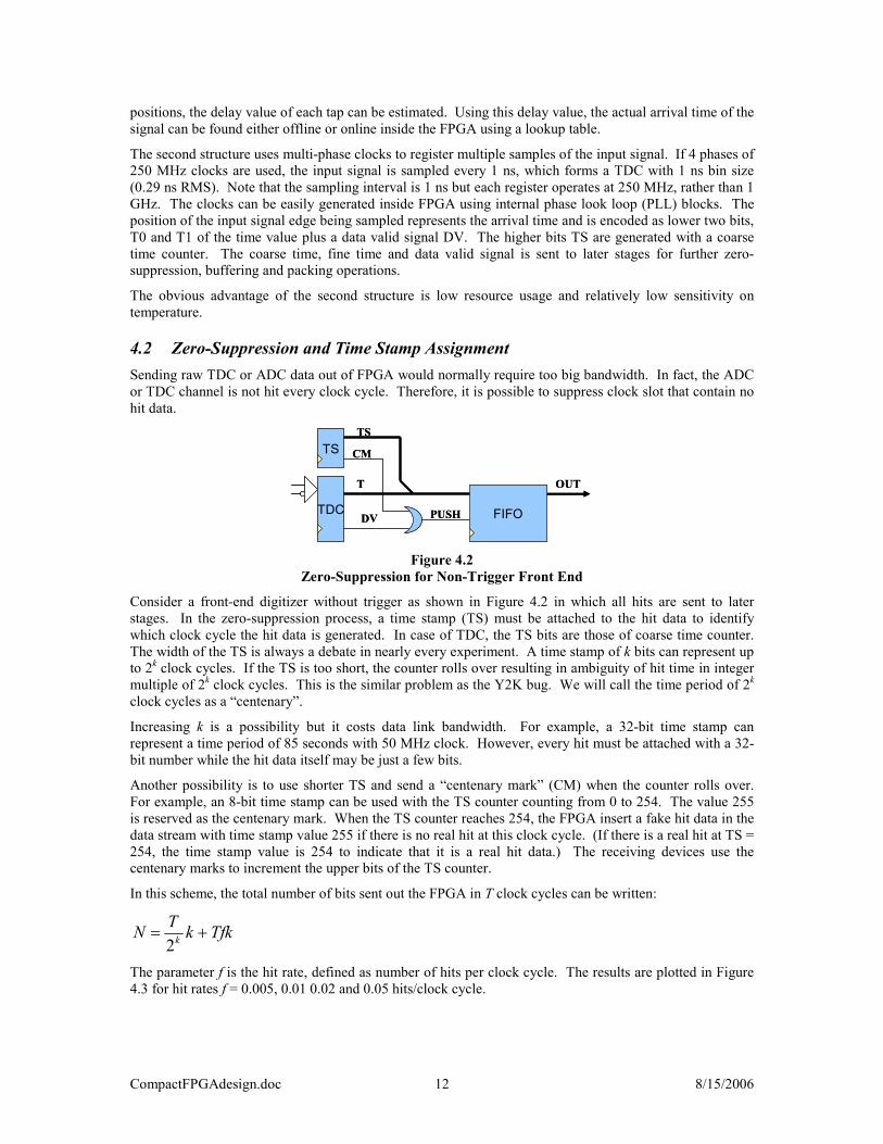
4.2 Zero-Suppression and Time Stamp Assignment Sending raw TDC or ADC data out of FPGA would normally require too big bandwidth. In fact, the ADC or TDC channel is not hit every clock cycle. Therefore, it is possible to suppress clock slot that contain no hit data.
TDC
TS
DV
TS
CM
T
FIFOPUSH
OUT
TDC
TS
DV
TS
CM
T
FIFOPUSH
OUT
Figure 4.2
Zero-Suppression for Non-Trigger Front End
Consider a front-end digitizer without trigger as shown in Figure 4.2 in which all hits are sent to later stages. In the zero-suppression process, a time stamp (TS) must be attached to the hit data to identify which clock cycle the hit data is generated. In case of TDC, the TS bits are those of coarse time counter. The width of the TS is always a debate in nearly every experiment. A time stamp of k bits can represent up to 2k clock cycles. If the TS is too short, the counter rolls over resulting in ambiguity of hit time in integer multiple of 2k clock cycles. This is the similar problem as the Y2K bug. We will call the time period of 2k
clock cycles as a “centenary”.
Increasing k is a possibility but it costs data link bandwidth. For example, a 32-bit time stamp can represent a time period of 85 seconds with 50 MHz clock. However, every hit must be attached with a 32-bit number while the hit data itself may be just a few bits.
Another possibility is to use shorter TS and send a “centenary mark” (CM) when the counter rolls over. For example, an 8-bit time stamp can be used with the TS counter counting from 0 to 254. The value 255 is reserved as the centenary mark. When the TS counter reaches 254, the FPGA insert a fake hit data in the data stream with time stamp value 255 if there is no real hit at this clock cycle. (If there is a real hit at TS = 254, the time stamp value is 254 to indicate that it is a real hit data.) The receiving devices use the centenary marks to increment the upper bits of the TS counter.
In this scheme, the total number of bits sent out the FPGA in T clock cycles can be written:
TfkkTN k +=2
The parameter f is the hit rate, defined as number of hits per clock cycle. The results are plotted in Figure 4.3 for hit rates f = 0.005, 0.01 0.02 and 0.05 hits/clock cycle.

CompactFPGAdesign.doc 13 8/15/2006
0
0.1
0.2
0.3
0.4
0.5
0.6
0.7
0.8
0.9
0 2 4 6 8 10 12 14 16 18
Number of bits of the time stamp
Num
bero
fbits
sent
outt
heFP
GA/
clco
ckcy
cle f=0
f=0.005f=0.01f=0.02f=0.05
Figure 4.3
Data Output Rate from the FPGA
It can be seen that with hit rate of around 1%, the FPGA output rate is minimum when the number of bits used for time stamp is 8-12. Long time stamp is only reasonable when the hit rate is extremely low.
The choice of the time stamp also depends on other factors like time needed for the accelerator turn. For example, an accelerator turn in Fermilab Tevtron is 159 clock cycles at clock period 132ns. It is more convenient to choose mod 3, mod 53 or mod 159 counters for corresponding bits of the TS counters.
4.3 Pipeline vs. FIFO Pipeline and FIFO buffers are two popular types of memory organization methods utilized in high energy physics trigger and DAQ systems. The names may not reflect the actual properties of the two buffer types. In fact, the data stored in and retrieved out of a pipeline is also in the first-in-first-out fashion. In this document, we use pipeline to refer a buffer with constant store to retrieve steps, which can be visualized as a serial-in-serial-out shift register. A FIFO buffer is a storage which data can be pushed into and popped out with same data orders for push and pop operations. The pipeline and FIFO buffers are shown in Figure 4.4.
CNT -L
RAM
QRARE
DWAWE
D Q D Q D Q D Q
CNT
RAM
QRARE
DWAWE
CNT
PUSH POP
D Q D Q D Q D QD QD Q
PUSH
CNT -L
RAM
QRARE
DWAWE RAM
QRARE
DWAWE
D Q D Q D Q D Q
CNT
RAM
QRARE
DWAWE RAM
QRARE
DWAWE
CNT
PUSH POP
D Q D Q D Q D QD QD Q
PUSH
Figure 4.4
Pipeline and FIFO Buffers
In a FIFO buffer, the write address (WA) and read address (RA) are kept with two counters. The write enable (WE) signal is derived from the PUSH signal which also increases the WA counter. In the output side, the read enable (RE) signal is derived from the POP signal that also increases the RA counter. Some varieties of the FIFO may have logic to check for empty (i.e., WA=RA) or full (i.e., WA-RA= number of RAM words -1) conditions. Sometime, additional logics are added to prevent outside circuit from pushing into a full or popping out an empty FIFO.

CompactFPGAdesign.doc 14 8/15/2006
The pipeline buffers can be viewed as shift registers but actually they are rarely implemented with shift registers chained up with flip-flops. The flip-flops are not efficient to store data not only in FPGA, but also in ASIC chips. Implementing long pipeline buffers with shift registers unnecessarily consumes large amount of silicon resource. Also, when data are clocked through flip-flops, transistors are turned on and off in all steps causing large power consumption.
The actual implementation of pipeline buffer is implemented similar as FIFO except the read address RA is derived from write address WA with WA-RA = L where L is the length of the pipeline. The RAM cell uses a lot less transistors than the flip-flop. After a data is stored in RAM, the transistors of the storage cell keep the on or off states unchanged until next time being overwritten, instead of changing every clock cycle as in flip-flops.
In high energy physics trigger and DAQ systems, pipelines are often used to store detector data for a fix number of clock cycles waiting for L1 trigger. The FIFO buffers, on the other hand, are used when the instantaneous data rate is considerably different from the average data rate such as in the zero-suppression process. A possible triggered front-end design that uses both pipeline and FIFO buffers is shown in Figure 4.5.
TDC
TS
DV
WAT
FIFOPUSH
OUT
PIPELINE DV
TRA
L1 FSM
Trigger Primitives
L1
TN
TDC
TS
DV
WAT
FIFOPUSH
OUT
PIPELINE DV
TRA
L1 FSM
Trigger Primitives
L1
TN
Figure 4.5
A Trigger Front-End
In this model front-end FPGA, the arrival times of the detector hits digitized in the TDC block with DV signal indicating that a valid hit is detected at the given clock cycle. The bits of T representing the arrival time of the detector hits along with the DV signal are written into the pipeline buffer every clock cycle, regardless these is a hit or not, and the time stamp TS is used as the write address WA. The immediate hit information, perhaps, just the DV signals of all channels are sent into the output data stream as trigger primitives.
Of course, the trigger primitives can also be more complicate. For example, the mean time of the arrival times of two adjacent channels can be used which represents the particle track hit time or event time (plus a constant delay) in drift chamber cases.
The trigger primitives are collected by the trigger/DAQ system and are used to generate a global level 1 trigger L1.
The L1 returns back to the front-end at the time when the hits from the trigger event are about to reach the end of the pipeline. Conducted by the L1 finite state-machine (FSM), non-empty data are pushed into the FIFO buffer. Now DV signal is used to derive the PUSH signal so that only non-empty data are pushed. However, additional bits must be included into the hit data. Usually, a trigger number TN or something similar is put into the trigger packet data header. For every hit, several bits of the read address RA that represent the coarse time must be added. The hit data pushed into the FIFO are sent out to the trigger/DAQ system when the output channel is not used to send the trigger primitives.
Also, it is not necessary to require the L1 return latency to be constant. The L1 trigger can be a multi-bit command and several bits in the command can be assigned as starting time stamp of the L1 window. The L1 FSM generates the corresponding read address RA that will ensure the hit data in correct timing window are collected. This scheme can be used in trigger systems when variable L1 trigger latency is necessary.
We shift our attention to comparison of the pipeline and the FIFO buffers. In the pipeline shown in previous example, many time slots contain no valid hits. It seems that zero-suppression should be done
CompactFPGAdesign.doc 15 8/15/2006
right after the TDC, rather than after receiving the L1 trigger. In other words, it appears to be more economical to replace the pipeline in Figure 4.5 with FIFO.
However, several factors must be considered while choosing zero-suppression stage. First, zero-suppression process increases data word width since the time stamp must be added, while in pipeline buffer, the read address RA itself is the time stamp. Second, in the FIFO used for zero-suppression, a WA and a RA counter must be kept for every channel, while in pipeline buffer the WA and RA are common for all channels.
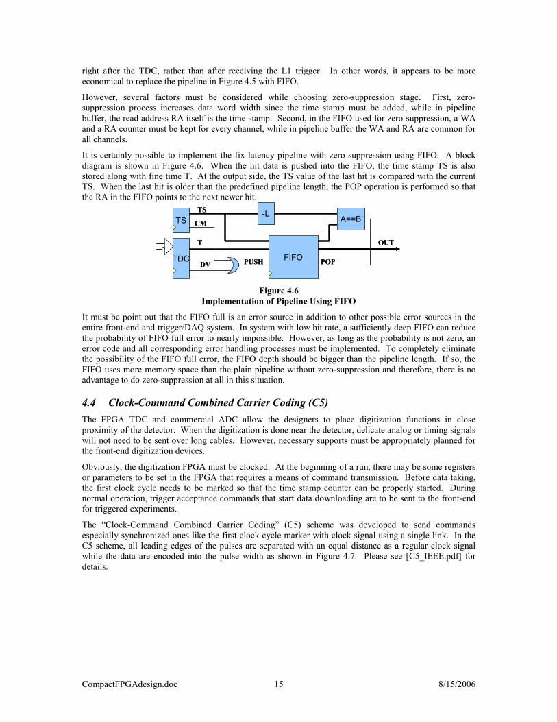
It is certainly possible to implement the fix latency pipeline with zero-suppression using FIFO. A block diagram is shown in Figure 4.6. When the hit data is pushed into the FIFO, the time stamp TS is also stored along with fine time T. At the output side, the TS value of the last hit is compared with the current TS. When the last hit is older than the predefined pipeline length, the POP operation is performed so that the RA in the FIFO points to the next newer hit.
TDC
TS
DV
TS
CM
T
FIFOPUSH
OUT
-LA==B
POPTDC
TS
DV
TS
CM
T
FIFOPUSH
OUT
-LA==B
POP
Figure 4.6 Implementation of Pipeline Using FIFO
It must be point out that the FIFO full is an error source in addition to other possible error sources in the entire front-end and trigger/DAQ system. In system with low hit rate, a sufficiently deep FIFO can reduce the probability of FIFO full error to nearly impossible. However, as long as the probability is not zero, an error code and all corresponding error handling processes must be implemented. To completely eliminate the possibility of the FIFO full error, the FIFO depth should be bigger than the pipeline length. If so, the FIFO uses more memory space than the plain pipeline without zero-suppression and therefore, there is no advantage to do zero-suppression at all in this situation.
4.4 Clock-Command Combined Carrier Coding (C5) The FPGA TDC and commercial ADC allow the designers to place digitization functions in close proximity of the detector. When the digitization is done near the detector, delicate analog or timing signals will not need to be sent over long cables. However, necessary supports must be appropriately planned for the front-end digitization devices.
Obviously, the digitization FPGA must be clocked. At the beginning of a run, there may be some registers or parameters to be set in the FPGA that requires a means of command transmission. Before data taking, the first clock cycle needs to be marked so that the time stamp counter can be properly started. During normal operation, trigger acceptance commands that start data downloading are to be sent to the front-end for triggered experiments.
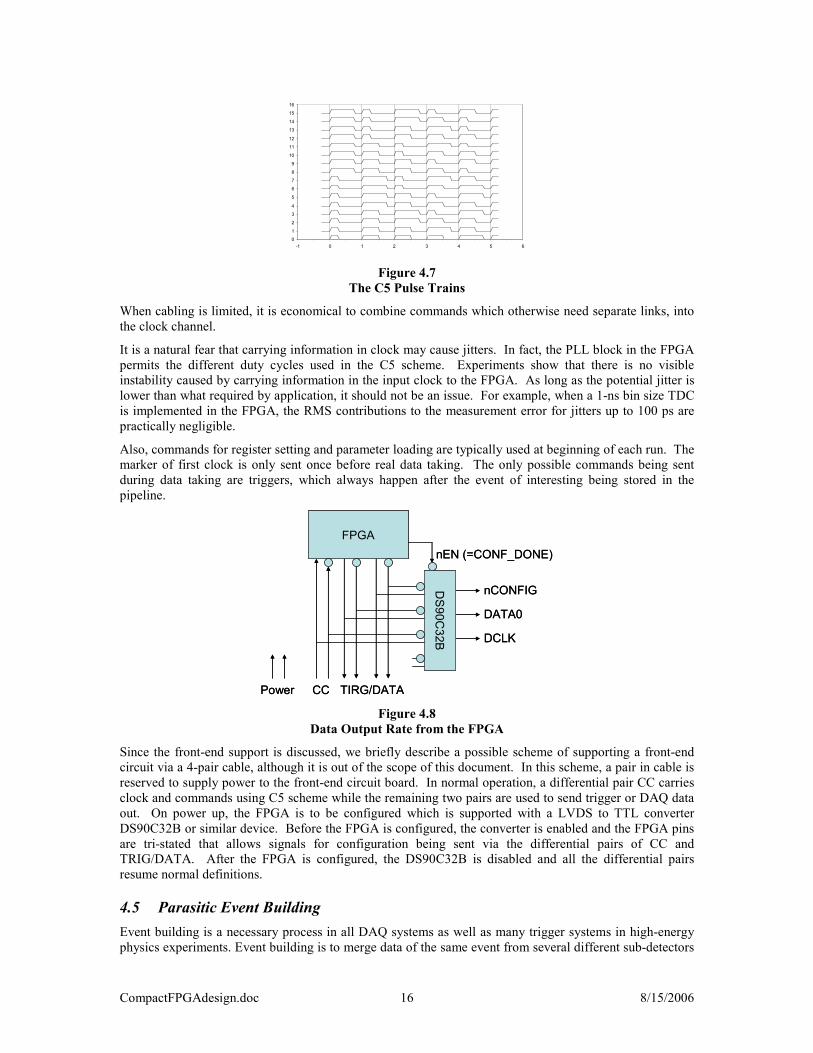
The “Clock-Command Combined Carrier Coding” (C5) scheme was developed to send commands especially synchronized ones like the first clock cycle marker with clock signal using a single link. In the C5 scheme, all leading edges of the pulses are separated with an equal distance as a regular clock signal while the data are encoded into the pulse width as shown in Figure 4.7. Please see [C5_IEEE.pdf] for details.
CompactFPGAdesign.doc 16 8/15/2006
0
1
2
3
4
5
6
7
8
9
10
11
12
13
14
15
16
-1 0 1 2 3 4 5 6
Figure 4.7
The C5 Pulse Trains
When cabling is limited, it is economical to combine commands which otherwise need separate links, into the clock channel.
It is a natural fear that carrying information in clock may cause jitters. In fact, the PLL block in the FPGA permits the different duty cycles used in the C5 scheme. Experiments show that there is no visible instability caused by carrying information in the input clock to the FPGA. As long as the potential jitter is lower than what required by application, it should not be an issue. For example, when a 1-ns bin size TDC is implemented in the FPGA, the RMS contributions to the measurement error for jitters up to 100 ps are practically negligible.
Also, commands for register setting and parameter loading are typically used at beginning of each run. The marker of first clock is only sent once before real data taking. The only possible commands being sent during data taking are triggers, which always happen after the event of interesting being stored in the pipeline.
FPGA
DS
90C32B
nEN (=CONF_DONE)
CC TIRG/DATAPower
DCLK
DATA0
nCONFIG
FPGA
DS
90C32B
nEN (=CONF_DONE)
CC TIRG/DATAPower
DCLK
DATA0
nCONFIG
Figure 4.8 Data Output Rate from the FPGA
Since the front-end support is discussed, we briefly describe a possible scheme of supporting a front-end circuit via a 4-pair cable, although it is out of the scope of this document. In this scheme, a pair in cable is reserved to supply power to the front-end circuit board. In normal operation, a differential pair CC carries clock and commands using C5 scheme while the remaining two pairs are used to send trigger or DAQ data out. On power up, the FPGA is to be configured which is supported with a LVDS to TTL converter DS90C32B or similar device. Before the FPGA is configured, the converter is enabled and the FPGA pins are tri-stated that allows signals for configuration being sent via the differential pairs of CC and TRIG/DATA. After the FPGA is configured, the DS90C32B is disabled and all the differential pairs resume normal definitions.
4.5 Parasitic Event Building Event building is a necessary process in all DAQ systems as well as many trigger systems in high-energy physics experiments. Event building is to merge data of the same event from several different sub-detectors

CompactFPGAdesign.doc 17 8/15/2006
together. When the operation rate of a detector increases, it is often necessary to distribute data of different events to different post-processors.
In today’s trigger/DAQ systems, event building is done primarily utilizing data switches to perform the merging and distributing functions. However, it is possible to spread the event building functions parasitically into pre-processing stages or even simple electronics modules like optical receiver or fan-out units. This way, a dedicated data switch can be eliminated. An example of parasitic event building architecture is given in [EvtBld_paper05_vMar06.pdf].
RAMZBT
128 x 4KB
FIFO/Hash Sorter
A
De-serial.
serial.
D
WA RA
32
Input Data Organization
De-serial.
Input Data Organization
De-serial.
Input Data Organization
RAMZBT
128 x 4KB
FIFO/Hash Sorter serial.FIFO
/Hash Sorter serial.FIFO/Hash Sorter serial.
FIFO/Hash Sorter serial.FIFO
/Hash Sorter serial.FIFO/Hash Sorter serial.FIFO
/Hash Sorter serial.
RA(10)
RA(10)
RAMZBT
128 x 4KB
FIFO/Hash Sorter
A
De-serial.De-
serial.
serial.serial.
D
WA RA
32
Input Data Organization
De-serial.De-
serial.
Input Data Organization
De-serial.De-
serial.
Input Data Organization
RAMZBT
128 x 4KB
FIFO/Hash Sorter serial.serial.FIFO
/Hash Sorter serial.serial.FIFO/Hash Sorter serial.serial.
FIFO/Hash Sorter serial.serial.FIFO
/Hash Sorter serial.serial.FIFO/Hash Sorter serial.serial.FIFO
/Hash Sorter serial.serial.
RA(10)
RA(10)
Figure 4.9 The Parasitic Event Building in an FPGA
As an example, the time stamp ordering FPGA for the BTeV level 1 pixel trigger system is shown in Figure 4.9. The inputs are 3 channels of serial links at 2.5 Gb/s which are de-serialized into parallel data. The input data are stored in two zero turn-around (ZBT) synchronous RAM devices and waited until data from a beam cross over (BCO) are believed to have all arrived. Then the data from a BCO are read back into FPGA and sent into one of the 8 output channels. Data for next BCO are given to next channel and so on.
The primary function of the FPGA is to perform the given pre-processing function, while it is also serve as a data merger and distributor. In other words, it performs a switch fabric function parasitically.
4.6 Digital Phase Follower Serial communication is a popular data transmission scheme since the communication channel is simply a twist-pair of a cable. There are serial transceivers available in several FPGA families with operating bit rate higher than 1 Gb/s. However, the costs of FPGA with build-in transceivers are normally higher than the comparable devices without transceivers. There are applications of serial communications to be implemented in low-cost FPGA families where there are no dedicated transceivers, but relatively lower bit rates are sufficient. The Digital Phase Follower (DPF) is developed to fill this gap.
The transmitter of serial data is relatively simple which is a parallel to serial converter implemented either with a shift register or dual-port memory with single-bit output port. The receiver is more complicate since the cable delay causes the data to arrive at any possible phases. When temperature of the cable varies, the phase of the serial data may drift away from the original phase. If the clocks of the sender and the receiver are not derived from the same source, a continuous and indefinite phase drift is expected.
The DPF uses multiple samples of the data stream to detect and to keep track of the input data phase. In each bit time, the input data is sampled 4 times at 0, 90 180 and 270 degrees. The 4 clocks (or 0 and 90

CompactFPGAdesign.doc 18 8/15/2006
degrees plus their inverted versions) can be generated with a PLL block now available in most low-cost FPGA families. The block diagram of the DPF is shown in Figure 4.10.
b0 b1 b2b0 b1 b2
c0
c90
c180
c270
c0In
MultipleSampling
ClockDomain
Changing
b0
b1
FrameDetection
DataOut
Tri-speedShift
Register
Shift2
Shift0
was3is0
SEL
was0is3
Trans.Detection
Q0
Q1
Q2
Q3QF
QE
QD
c0
c90
c180
c270
c0In
MultipleSampling
ClockDomain
Changing
b0
b1
FrameDetection
DataOut
Tri-speedShift
Register
Shift2
Shift0
was3is0
SEL
was0is3
Trans.Detection
Q0
Q1
Q2
Q3QF
QE
QD
Figure 4.10
The Multi-sampling and Digital Phase Follower
The multi-sampling part is the same as in FPGA TDC discussed before. In fact, the operation of the DPF is based on the transition time of the input data stream. After multi-sampling, the sampled pattern is first converted to the 0 degree clock domain. Then 7 samples, QD to Q3 are sent to the transition detection logic to find the relative phase of the input data as shown in Figure 4.11. Note that the sample pattern jumps up 4 bits every clock cycles, i.e., QD jumps to Q1, QE to Q2 and QF to Q3 which is obvious from the pipeline structure shown in Figure 4.10.
b0
SEL
Q0
Q1
Q2
Q3
QF
QE
QD
Newer Samples
Older Samples
SelectedSample
SelectedSample
SelectedSample
SelectedSample
SEL=0 SEL=1 SEL=2 SEL=3
b0
SEL
Q0
Q1
Q2
Q3
QF
QE
QD
Newer Samples
Older Samples
SelectedSample
SelectedSample
SelectedSample
SelectedSample
SEL=0 SEL=1 SEL=2 SEL=3 Figure 4.11
The Transition Detection in the Digital Phase Follower
The designers may choose to detect both 0-to-1 and 1-to-0 transitions, but detecting only one transition is recommended since the raising and falling time of the input circuit may be different. Once the first transition is seen, the location of it is registered and the data sample sufficiently far away from the transition points is selected as an input of the shift register in the later stage. For example, when a 0-to-1 transition is seen between QF and QE, i.e., (QF==0)&&(QE==1), the sample Q0 is selected, and so on.
When the phase of the input data drifts away from the original point, the transition at different location is detected. The sample point being selected follows the change of the transition location change accordingly.
As mentioned earlier, the input data phase may drift indefinitely if the clocks of the sender and receiver have very close but slightly different frequencies. Even in the systems with same clock source for the sender and receiver, the phase drift due to cable temperature variation may also be bigger than a bit time.

CompactFPGAdesign.doc 19 8/15/2006
We can assume that the phase drift rate is not too high so that position of the current transition is either the same as what previously detected, or +1 or -1 from the previous position. Under this assumption, there are two possible cases for the bit phase drifting out of one bit time. The two cases: “was-0-is-3” and “was-3-is-0” are shown in Figure 4.12.
Q0
Q1
Q2
Q3
QF
QE
QD
OldSelection
NewSelection
SEL was 0 SEL is 3
b0
b1
Tri-speedShift
Register
Shift2
Shift0
SEL
was0is3
Q0
Q1
Q2
Q3
Newer Samples
Older Samples
Q0
Q1
Q2
Q3
QF
QE
QD
OldSelection
NewSelection
SEL was 0 SEL is 3
b0
b1
Tri-speedShift
Register
Shift2
Shift0
SEL
was0is3
Q0
Q1
Q2
Q3
Newer Samples
Older Samples
Q0
Q1
Q2
Q3
QF
QE
QD
NewSelection
OldSelection
SEL was 3 SEL is 0
b0
b1
Tri-speedShift
Register
Shift2
Shift0
was3is0
SEL
Q0
Q1
Q2
Q3
Newer Samples
Older Samples
Q0
Q1
Q2
Q3
QF
QE
QD
NewSelection
OldSelection
SEL was 3 SEL is 0
b0
b1
Tri-speedShift
Register
Shift2
Shift0
was3is0
SEL
Q0
Q1
Q2
Q3
Newer Samples
Older Samples
Figure 4.12
The Digital Phase Following Processes
The first case is finding the transition between Q2 and Q1 requesting that the sample Q3 being selected in current clock cycle while the previously registered selection was Q0. This was-0-is-3 case indicates that the input data clock is slower than the local clock. The selection point is actually drifted from Q0 to QF. However, to prevent the sampling point from drifting down indefinitely, it is wrapped over to Q3 instead of QF. Since the current sample at Q3 has been shifted into the shift-register in previous clock cycle (which was Q0), the shift register stops shifting for one clock cycle to compensate for the slower input data clock.
The second case is finding the transition between QF and QE requesting that the sample Q0 being selected in current clock cycle while the previously registered selection was Q3. This was-3-is-0 case indicates that the input data clock is faster than the local clock. The selection point is actually drifted from Q3 to Q4 (which is not implemented). However, to prevent the sampling point from drifting up indefinitely, it is wrapped over to Q0. In this situation, two sample points, i.e., Q3 and Q0 must be pushed into the shift register causing it shift by 2 bits in the current clock cycle to compensate for the faster input data.
The shift register normally shifts by 1 and it shifts by 0 or by 2 in the “was-0-is-3” or “was-3-is-0” cases, respectively, which is why it is called “tri-speed shift register”. Typical de-serialization circuits, either in FPGA or single IC chip, recover the receiving clock using either PLL or clock swapping schemes. The digital phase follower is a pure digital circuit and the clock recovery is avoided.
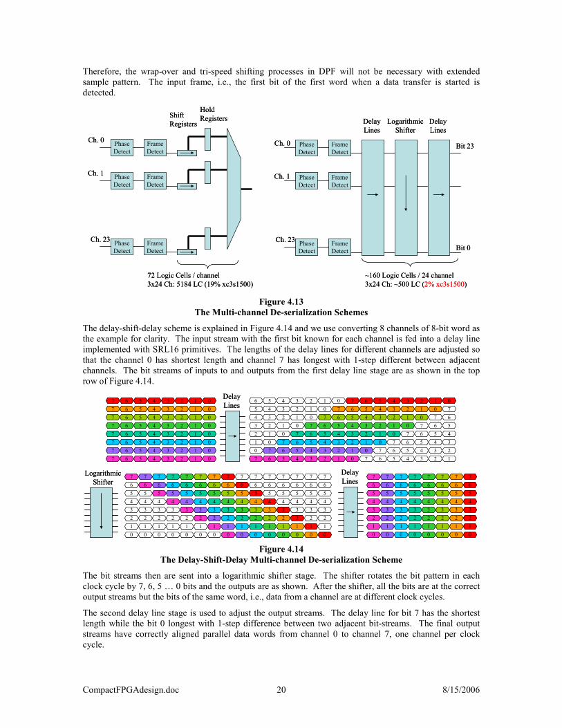
4.7 Multi-channel De-serialization Typical serial-to-parallel conversion uses shift register plus hold register scheme as shown in left of Figure 4.13. For data concentration applications where many serial channels are to be converted to parallel words and merged together, relatively large amount of logic cells may be needed. Use BTeV pixel readout system as an example where each channel outputs bit stream representing 24-bit words and up to 72 channels are to be merged together.
If the data channels are driven by the same clock source and cable delay variation is expected less than several bit time, a de-serialization scheme, delay-shift-delay scheme as shown in the right of Figure 4.13 with relatively small resource usage can be applied.
The delay-shift-delay scheme takes advantage of SRL16 primitives found in Xilinx FPGA devices. The SRL16 primitive is actually the 16x1-bit RAM used for the 4-input look-up table in each logic cell. The RAM can be configured as a 16-step serial-in-serial-out shift register that can be used as a delay line which would need 16 logic cells if implemented otherwise. See [XAPP465] for detail description of SRL16.
The delay-shift-delay scheme is developed based on [XAPP194] with modifications. All serial inputs are checked for the transition phase using schemes like the digital phase follower as described earlier. The clocks driven all channels are derived from the same source so the phases of inputs will not drift indefinitely and the variation of the cable delay is expected to be less than certain number of bit times.
CompactFPGAdesign.doc 20 8/15/2006
Therefore, the wrap-over and tri-speed shifting processes in DPF will not be necessary with extended sample pattern. The input frame, i.e., the first bit of the first word when a data transfer is started is detected.
ShiftRegisters
Ch. 0
72 Logic Cells / channel3x24 Ch: 5184 LC (19% xc3s1500)
PhaseDetect
FrameDetect
HoldRegisters
PhaseDetect
FrameDetect
PhaseDetect
FrameDetect
Ch. 1
Ch. 23
ShiftRegisters
Ch. 0
72 Logic Cells / channel3x24 Ch: 5184 LC (19% xc3s1500)
PhaseDetect
FrameDetect
HoldRegisters
PhaseDetect
FrameDetect
PhaseDetect
FrameDetect
Ch. 1
Ch. 23
Delay Lines
Ch. 0
~160 Logic Cells / 24 channel3x24 Ch: ~500 LC (2% xc3s1500)
PhaseDetect
FrameDetect
LogarithmicShifter
PhaseDetect
FrameDetect
PhaseDetect
FrameDetect
Ch. 1
Ch. 23
Bit 23
Bit 0
Delay Lines
Delay Lines
Ch. 0
~160 Logic Cells / 24 channel3x24 Ch: ~500 LC (2% xc3s1500)
PhaseDetect
FrameDetect
LogarithmicShifter
PhaseDetect
FrameDetect
PhaseDetect
FrameDetect
Ch. 1
Ch. 23
Bit 23
Bit 0
Delay Lines
Figure 4.13 The Multi-channel De-serialization Schemes
The delay-shift-delay scheme is explained in Figure 4.14 and we use converting 8 channels of 8-bit word as the example for clarity. The input stream with the first bit known for each channel is fed into a delay line implemented with SRL16 primitives. The lengths of the delay lines for different channels are adjusted so that the channel 0 has shortest length and channel 7 has longest with 1-step different between adjacent channels. The bit streams of inputs to and outputs from the first delay line stage are as shown in the top row of Figure 4.14.
4567 01234567 01234567 01234567 01234567 01234567 01234567 01234567 0123
4567 01234567 01234567 01234567 01234567 01234567 01234567 01234567 0123
DelayLinesDelayLines
4567 01234567 0123
4567 01234567 0123
4567 01234567 0123
4567 01234567 0123
456 012345 70123
4 67012356701234567012
456701 345670 23
4567 123
4567 01234567 0123
4567 01234567 0123
4567 01234567 0123
4567 01234567 0123
456 012345 70123
4 67012356701234567012
456701 345670 23
4567 123
LogarithmicShifter
LogarithmicShifter
45
67
01
23
45
67
01
23
45
67
01
23
45
67
01
23
45
67
01
23
45
67
01
23
45
67
01
23
45
67
01
23
45
6
01
23
45
7
01
23
4
67
01
23
56
7
01
23
45
67
01
2
45
67
01
34
56
7
0
23
45
67
12
34
56
7
01
23
45
67
01
23
45
67
01
23
45
67
01
23
45
67
01
23
45
67
01
23
45
67
01
23
45
67
01
23
45
6
01
23
45
7
01
23
4
67
01
23
56
7
01
23
45
67
01
2
45
67
01
34
56
7
0
23
45
67
12
3
DelayLinesDelayLines
4567
0123
4567
0123
4567
0123
4567
0123
4567
0123
4567
0123
4567
0123
4567
0123
4567
0123
4567
0123
4567
0123
4567
0123
4567
0123
4567
0123
4567
0123
4567
0123
Figure 4.14 The Delay-Shift-Delay Multi-channel De-serialization Scheme
The bit streams then are sent into a logarithmic shifter stage. The shifter rotates the bit pattern in each clock cycle by 7, 6, 5 … 0 bits and the outputs are as shown. After the shifter, all the bits are at the correct output streams but the bits of the same word, i.e., data from a channel are at different clock cycles.
The second delay line stage is used to adjust the output streams. The delay line for bit 7 has the shortest length while the bit 0 longest with 1-step difference between two adjacent bit-streams. The final output streams have correctly aligned parallel data words from channel 0 to channel 7, one channel per clock cycle.

CompactFPGAdesign.doc 21 8/15/2006
5 Several Examples for Daily Design Jobs
5.1 Temperature Digitization of TMP03/04 Devices The TMP03/TMP04 is a monolithic temperature detector that generates a modulated serial digital output that varies in direct proportion to the temperature of the device. The output of the device is a square wave of approximately 35 Hz. The pulse high time T1 is approximately 10 ms and is less sensitive to the temperature, while the pulse low time T2 varies from about 15 ms to 44 ms depending on the temperature.
The formula between the temperature and the duty cycle can be written:
Temperature (o C) = 235 – 400*T1/T2
The time intervals T1 and T2 can be measured fairly easily with counters. However, a division, a multiplication and a subtraction is necessary to calculate the temperature. Perhaps, the simplest implementation is to keep two counters for the two time intervals and to read the values of the two counters into a micro-processor. The arithmetic operations necessary in calculating the temperature can be done in the micro-processor.
If the temperature is to be calculated in the FPGA, not only time interval measurement, but also arithmetic operations must be carefully planned. Surely, there are divider and multiplier macro function libraries but they are normally for large amount of fast computations and occupies large amount of silicon resources. In temperature measurement, many clock cycles are to be spent counting the lengths of the time intervals T1 and T2, so smaller (although slower) arithmetic functions would be ideal.
Here, we discuss a counter-based circuit as shown in Figure 5.1. In this scheme, the arithmetic operations are performed during counting time intervals T2 and T1. This may not be the best circuit for all applications, but we will use it as an example to illustrate alternative approaches when arithmetic operations are needed in FPGA.
Counter24SCLRT2EN
Counter16 Mod XNSCLRXNT1x25ENT2N
T2N>>8 Counter12SCLREN
3760-A D Q
EN
Control FSMSCLRT2EN
T1x25ENDV
IN
DV
T2T1, 1st T1, 2nd T1, 25th
T16CCounter24SCLRT2EN
Counter16 Mod XNSCLRXNT1x25ENT2N
T2N>>8 Counter12SCLREN
3760-A D Q
EN
Control FSMSCLRT2EN
T1x25ENDV
IN
DV
T2T1, 1st T1, 2nd T1, 25th
T16C
Figure 5.1
The Temperature Digitization Circuit
The temperature output from the circuit above is an integer with LSB being 1/16 (o C). The equation above for this case can be written:
T16C (1/16 o C) = 16*235 - 16*400*T1/T2 = 3760 - 25*T1/(T2/256) = 3760 - 25*T1/(T2N>>8)
The modulated square wave IN signal is sent to the control finite state-machine (Control FSM). The FSM first generates a clear signal SCLR to reset all counters. Then, during the first IN = low time interval, signal T2EN is active which enables a 24-bit counter (Counter24) to count the length of T2 and the result is a 24-bit integer T2N. With 50 MHz system clock, T2N may have 22 non-zero bits. The shift right operation is simply ignoring the lower 8 bits and taking only the top 16 bits.
The next 16-bit counter (Counter16) uses the (T2N>>8) input as mod divisor. It outputs a pulse every (T2N>>8) clock cycles. The output then enables a 12-bit counter (Counter12) to increase by 1 each time.
CompactFPGAdesign.doc 22 8/15/2006
The Counter16 is enabled by the signal T1x25EN which is active during the input IN becomes high for 25 such intervals. The output of the Counter12 then represents the integer value 25*T1/(T2N>>8).
After 25 T1 intervals are counted, the FSM generates a data valid signal DV which enables the output register to update the new temperature value. The output of Counter12 flows through an adder that subtract 25*T1/(T2N>>8) from a constant 3760. The registered result T16C is an integer in unit of 1/16 (o C). It is refreshed every 25 T1 intervals or about 0.7 sec which is sufficient for most applications.
The division in this scheme is absorbed into the counting of Counter16 and Counter12. The multiplication of 16*400 is split into factors 25 and 256 and is done by counting 25 T1 intervals and by bit shifting on T2N, respectively.
5.2 Silicon Serial Number (DS2401) Readout The DS2401 is a 1-Wire bus device that provides a unique 64-bit registration number (which contains 8-bit family code + 48-bit serial number + 8-bit CRC tester). The 1-Wire bus devices have only two connected pins, a ground and a data (DQ). The DQ pin is pulled up through a resister and all I/O accesses are through the DQ pin. (Probably the device obtains power from the DQ pin also.)
It takes three operations to read out the number from the DS2401 device. During the first step, the master FPGA or micro-processor drives the DQ line low for more than 480 µs to initialize the DS2401 device.
In the second step, the master writes an 8-bit command 0Fh (or 33h) to the DS2401 indicating that the device is to be read. To write a bit with value 1, the master drives the DQ wire low for a short period of time (1 to 15 µs) and releases it. The DS2401 senses the DQ wire level to be 1 in the sampling window since DQ is pulled up by the resistor. To write a bit with value 0, the master drives the DQ wire low for a longer period of time (60 to 120 µs) that covers the sampling window of the DS2401, resulting in a 0 level being detected. Once the 8-bit sequence 1,1,1,1,0,0,0,0 (0Fh, LSB first) or 1,1,0,0,1,1,0,0 (33h, LSB first) is written into the DS2401, it is ready to output its contents.
The master reads out 64 bits in the third step. To read each bit, the master drives the DQ wire low for short time and releases it. The master then senses the DQ wire to determine if the output from the DS2401 is low or high. The reading sequence is also LSB first.
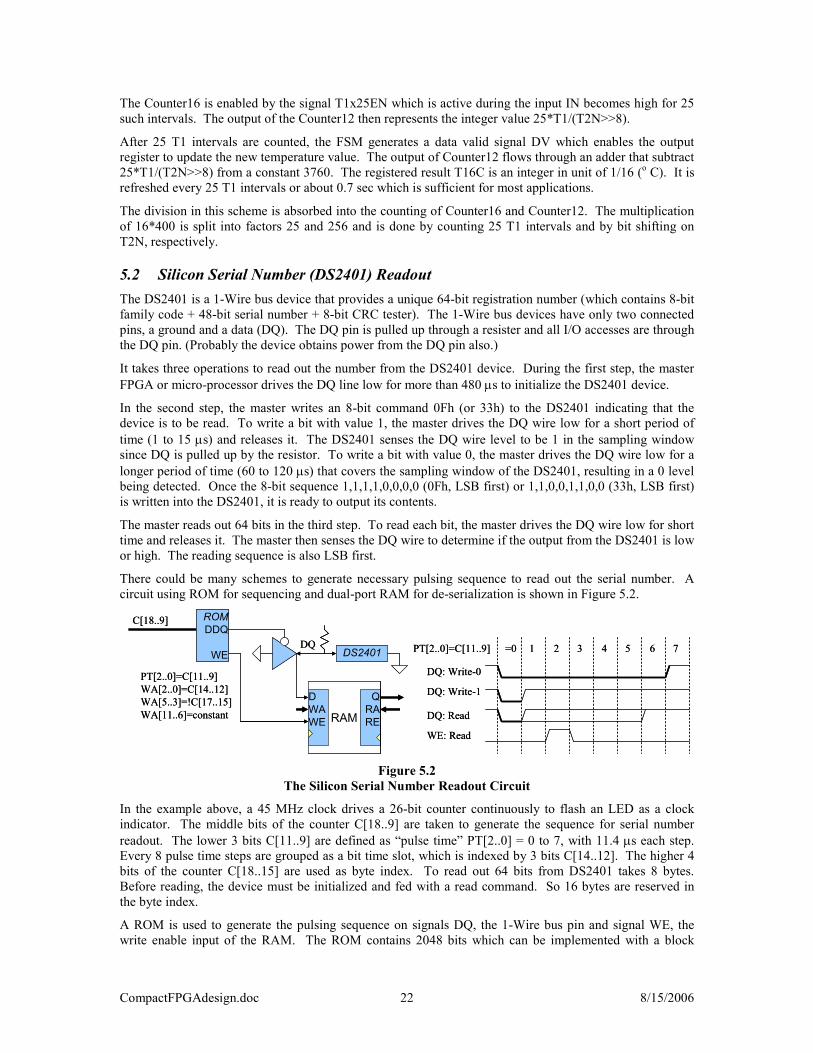
There could be many schemes to generate necessary pulsing sequence to read out the serial number. A circuit using ROM for sequencing and dual-port RAM for de-serialization is shown in Figure 5.2.
RAM
QRARE
DWAWE
C[18..9] ROMDDQ
WEDQ
PT[2..0]=C[11..9]WA[2..0]=C[14..12]WA[5..3]=!C[17..15]WA[11..6]=constant
DS2401
RAM
QRARE
DWAWE RAM
QRARE
DWAWE
C[18..9] ROMDDQ
WEDQ
PT[2..0]=C[11..9]WA[2..0]=C[14..12]WA[5..3]=!C[17..15]WA[11..6]=constant
DS2401 PT[2..0]=C[11..9] =0 1 2 3 4 5 6 7
DQ: Write-0
DQ: Write-1
DQ: Read
WE: Read
PT[2..0]=C[11..9] =0 1 2 3 4 5 6 7
DQ: Write-0
DQ: Write-1
DQ: Read
WE: Read
Figure 5.2 The Silicon Serial Number Readout Circuit
In the example above, a 45 MHz clock drives a 26-bit counter continuously to flash an LED as a clock indicator. The middle bits of the counter C[18..9] are taken to generate the sequence for serial number readout. The lower 3 bits C[11..9] are defined as “pulse time” PT[2..0] = 0 to 7, with 11.4 µs each step. Every 8 pulse time steps are grouped as a bit time slot, which is indexed by 3 bits C[14..12]. The higher 4 bits of the counter C[18..15] are used as byte index. To read out 64 bits from DS2401 takes 8 bytes. Before reading, the device must be initialized and fed with a read command. So 16 bytes are reserved in the byte index.
A ROM is used to generate the pulsing sequence on signals DQ, the 1-Wire bus pin and signal WE, the write enable input of the RAM. The ROM contains 2048 bits which can be implemented with a block

CompactFPGAdesign.doc 23 8/15/2006
memory in FPGA. In fact, there are many unchanging and repeating sections in the sequence so that the whole ROM can also be composed with a few small sub-ROM pieces which can be implemented with the LUT resources in the logic elements.
The initiation uses entire time at byte time 5, i.e., C[18..15]=5, which is 728 µs long, followed by another 728 µs device recover time during byte time 6. The byte time 7 is used to feed read command to the DS2401, which contains 4 Write-1 and 4 Write-0 bit time slots. The read sequence uses byte times 8-15, during which the WE become active at PT=2 in each bit time slot so that the data from the DS2401 can be written into the RAM.
The write and read ports of the RAM are 1-bit and 16-bit wide, respectively. Data are written into the RAM bit by bit and read out as a 16-bit word. The write address are simply derived from the counter bits C[17..12]. Note that the bit, byte or word order can be reversed to fit requests of different applications. For example, to maintain bit order and reverse the order of all 8 bytes, let WA[2..0]=C[14..12] but WA[5..3]=!C[17..15].
The RAM block in our example has 4096 memory bits, while the silicon serial number uses only 64. The higher bits of the WA are set as a constant so that the 64-bit silicon serial number is placed in the pre-defined location.
Clearly, it is also possible to use a shift register to convert serial stream into parallel words and indeed it is a more classical approach. In our example, the contents of the RAM block are initialized into ASCII characters so that it is read out as an ID block and the silicon serial number of the module is embedded into the ID block automatically. If using shift register, the ID block and the shift register are two data sources and they have to be merged together into the readout data path with a multiplexer. Also, other miscellaneous serial data such as temperature, power supply voltages can also be merged into the RAM block that provides a one-stop ID/status block for system diagnostic process.
6 Several Examples for Advanced Trigger Systems
6.1 Trigger Primitive Creation The flexibilities that FPGA devices provide make it possible to build trigger systems that produce advanced event identification abilities only available in software trigger or offline analysis stage in traditional experiments. We use a time-of-flight (TOF) detector shown in Figure 6.1 as an example, assuming the discriminated logic level signals from photo multiplier tubes (PMT) are sent to an FPGA.
TDC
TDV
TDC
TDV
+
-
TH - TC
ZH /C
TDC
TDV
TDC
TDV
+
-
TH - TC
ZH /C
Figure 6.1 Time-of Flight (TOF) Detector and Trigger Primitives
At a first look, there is not much can be done in the FPGA. In time domain, the signal arrival time depends on velocity of the particle and the position of the hit on the TOF counter. In space, the hits of particles from the two-body decay are not separated 180o “back-to-back”. The separation angle depends on the decay momentum and polar angle of the tracks.
Traditionally, input hit signals are stretched to cover latest arrivals. Using the stretched signals, some approximate coincidence, probably covering a wide range of azimuth angle can formed.
However, if the arrival times of the input signals are digitized using TDC schemes presented before to the precision of about 0.5 ns, interesting features of the events in several aspects can be extracted. (Note that

CompactFPGAdesign.doc 24 8/15/2006
the TDC in FPGA normally is not precise enough for offline data analysis so separate TDC devices for DAQ system are still needed. The TDC in FPGA here is for trigger purposes only.)
Assuming the PMT signal arrival times from both ends of a counter are TA and TB, respectively. Then the time of charged particle hitting the counter TH and the hit position ZH can be approximately found by simply adding and subtracting two arrival times:
)(2/)(
BAH
CBAH
TTCZTTTT
−=++=
The parameter TC and C are known constants for given size of the TOF counter. The z-measurement can be good to about 10 cm with TDC of 0.5 ns precision or better. With z-positions of charged particle hits, the 3-D feature of the event is available allowing the user to identify the type of the event and provide advanced trigger primitives to the global trigger.
0
2
4
6
8
10
12
14
0 0.2 0.4 0.6 0.8 1 1.2 1.4
Z (m)
TOF
(ns)
0.40.50.60.70.80.91
Figure 6.2 The Time-of Flight (TOF) as Function of Hit Position
In Figure 6.2, the times-of-flight as functions of hit position Z in a TOF detector with radius 0.8 m and half-length 1.2m for different β values are plotted. With time measurements good to 0.5 ns, one should be able to distinguish a slow and a fast particle hit.
Some background like collision of beam particle with residual gas comes earlier than fast particle which can be easily identified.
The z-position of the hit itself is very useful also. It is possible the check back-to-back condition in not only x-y projection, but also r-z projection. For example, in a two-body decay event with two opposite charged particles, once the polar angle of the decay tracks is known, decay momentum can be estimated from the separation of hits in azimuth dimension. Combining the fast/slow particle identification, the types of the event can be classified fairly well.
The hit positions can also be checked with other detectors in global trigger stage.
6.2 Unrolling Nested-Loops, Doublet Finding In HEP trigger systems, sometimes data items from two sets are to be paired up. Consider an example shown in Figure 6.3 with two (or more) detector planes detecting tracks come from a known interaction point chosen as the origin. Magnetic field is in y-direction so that the x-z is the bend view and the y-z is the non-band view. To reconstruct tracks, hits on different detector planes generated by the same track are to be paired up.
In the non-bend view, a constraint, i.e., a necessary condition for two hits to belong to a track exists. Clearly, the y-coordinates of two hits from same track must satisfy the following condition:

CompactFPGAdesign.doc 25 8/15/2006
3
3
1
1
Zy
Zy ii =
The parameters Z1 and Z3 are known constants, representing the distances of the two detector planes to the interaction point.
In practice, the constraint is an inequality to allow errors from either coordinate measurement or the model itself:
εε −>>+ iii yyZZy 13
3
11
y
xz
y1i
y1j
x1i
x1j
y3i
y3j
x3i
x3j
y
xz
y1i
y1j
x1i
x1j
y3i
y3j
x3i
x3j
Figure 6.3
A Hit Pairing Problem
In software, pairing up two data items is implemented with two layers nested loops, assuming in an event, there are n1 and n3 hits on the two detector planes: for(i1=0; i1<n1; i1++){ for(i3=0; i3<n3; i3++){ CheckCondition(y1[i1], y3[i3]); } }
The execution time of the process is O(n2) where n is number of hits on the two planes in an event.
In an online trigger system, the process time must cope with the data fetching time which is proportional to the number of hits on a detector plane, i.e., O(n). It is then necessary to reduce the execution time of the process by “unrolling” a layer of the nested loops.
6.2.1 Functional Block Arrays
In principle, it is possible to implement multiple copies of a function in the FPGA so that multiple operations of a given function can be performed in each clock cycle. Since multiple copies are created, the functional block array consumes silicon resource rapidly. To reduce silicon usage, the function should be analyzed and operations that can be done outside the array should be extracted as much as possible.
In the hit matching process, for example, hit coordinates from two different detector planes are to be paired up. It is possible to design a functional block array as shown in Figure 6.4. The hit coordinates from one plane are first loaded in to the array and are stored in u1, u2, etc. (corresponding to y3i, y3j etc.). Then the hit

CompactFPGAdesign.doc 26 8/15/2006
coordinate x (corresponding to y1i, y1j etc.) from another plane for each hit is fetched in and all functional blocks check the matching conditions with pre-stored values u1, u2, etc. simultaneously. The process repeats for next hit coordinate x until all hits are looped through.
S- x …u1
F(u,x)
> <
u x
u2
u M F(u,x)
S- x …u1
F(u,x)
> <
u x
u2
u M F(u,x)
u1
u x-b
u2
u M
>< &
><
><
&
&
x+a
u1
u x-b
u2
u M
>< &
><
><
&
&
x+a
5.06119E+1927878400 1.81545E+12
2.72E+221.34E+23
0
4
8
12
16
0 4 8 12 16
X
U
Low
Hi
PhysL
PhysH
Figure 6.4
A Functional Block Array for Range Cutting
It is possible to extract the operations common for all blocks, leaving two comparison operations in each functional block. The hit coordinates from one plane are first scaled and stored in u1, u2, etc. The coordinates from another plane are then added and subtracted with two constants: a and b representing errors in the hit matching constraint. For each x, the pre-stored values u1, u2, etc. are compared with the upper and lower boundaries (x + a) and (x - b), respectively. If a pre-stored value falls inside the boundary, two hits possibly form a track are paired up together.
If there are m and n hits/event in each detector plane, then the execution time for the whole process takes about (m + n) clock cycles, if m<M where M is number of blocks implemented in the array. The execution time of the process is then reduced from O(n2) to O(n) at the cost of multiple copies of the comparator blocks.
The functional block array above is significantly smaller than that if the addition and subtraction operations are performed in each array element. The acceptance map has relatively smooth upper and lower boundaries if sufficient bits are implemented in the comparators.
u1
u
u2
u M
====
xx+1
====
====
u1
u
u2
u M
====
xx+1
====
====
5.06119E+1927878400 1.81545E+12
2.72E+221.34E+23
0
4
8
12
16
0 4 8 12 16
X
U
Low
Hi
PhysL
PhysH
Figure 6.5
A Functional Block Array of Multi-Equality
It is possible to further replace magnitude comparators with equality comparators as shown in Figure 6.5. If implemented with FPGA logic elements, the equality comparator is about half the size of the magnitude comparator of same number of bits. The trade of is, however, the boundaries in the acceptance map become a relative rough saw-teeth shape.

CompactFPGAdesign.doc 27 8/15/2006
A functional block array with M block checks up to M pairs of data simultaneously. It “unrolls” the inner most loop if the number of hits m in the inner most loop is <M. If m>M, multiple passes of operation will be needed.
6.2.2 Contents Addressable Memory (CAM)
The contents addressable memory (CAM) can be viewed as a functional block array checking single equality as shown in Figure 6.6. The real CAM uses only two additional transistors per memory cell so it is very resource conserving given the complexity of the function that CAM performs.
M2M1
M3 M4M5 M6
M7 M8
B+ B-
A+ A-
EQ-
WL
M2M1
M3 M4M5 M6
M7 M8
B+ B-
A+ A-
EQ-
WL
u1
u
u2
u M
==
x
==
==
u1
u
u2
u M
==
x
==
==
5.06119E+1927878400 1.81545E+12
2.72E+221.34E+23
0
4
8
12
16
0 4 8 12 16
X
U
Low
Hi
PhysL
PhysH
Figure 6.6 The Contents Addressable Memory as a Single Equality Functional Block Array
In FPGA, however, not so many families have the real CAM resources and it takes large amount silicon resources if “implemented” with logic elements. If large amount of data items with large word width are to be checked, external CAM device can be considered as an option.
The CAM checks single equality between the input data and the pre-stored data. An obvious issue is the missing boundary area in the acceptance map. To cover the missing boundary, one may consider using two CAM devices to check for double-equality. If there are several clock cycles available for each write and/or read operation, several slightly varied data can be stored into the CAM, or several comparisons can be performed during read to cover the missing boundary areas.
Typically, the CAM devices are designed to make single match like finding unique IP address in network equipments. Special cares must be taken to handle multiple matching situations which are very common in HEP applications.
6.2.3 Hash Sorter
The Hash Sorter is better suited in HEP applications in terms of silicon resource usage, multiple data items handling etc. for data item matching processes. The hash sorter is implemented using block RAM and logic element resources found in any FPGA. Please read [hashsNIM04.pdf] and [HashSorter03.pdf] for details.
Figure 6.7 The Hash Sorter
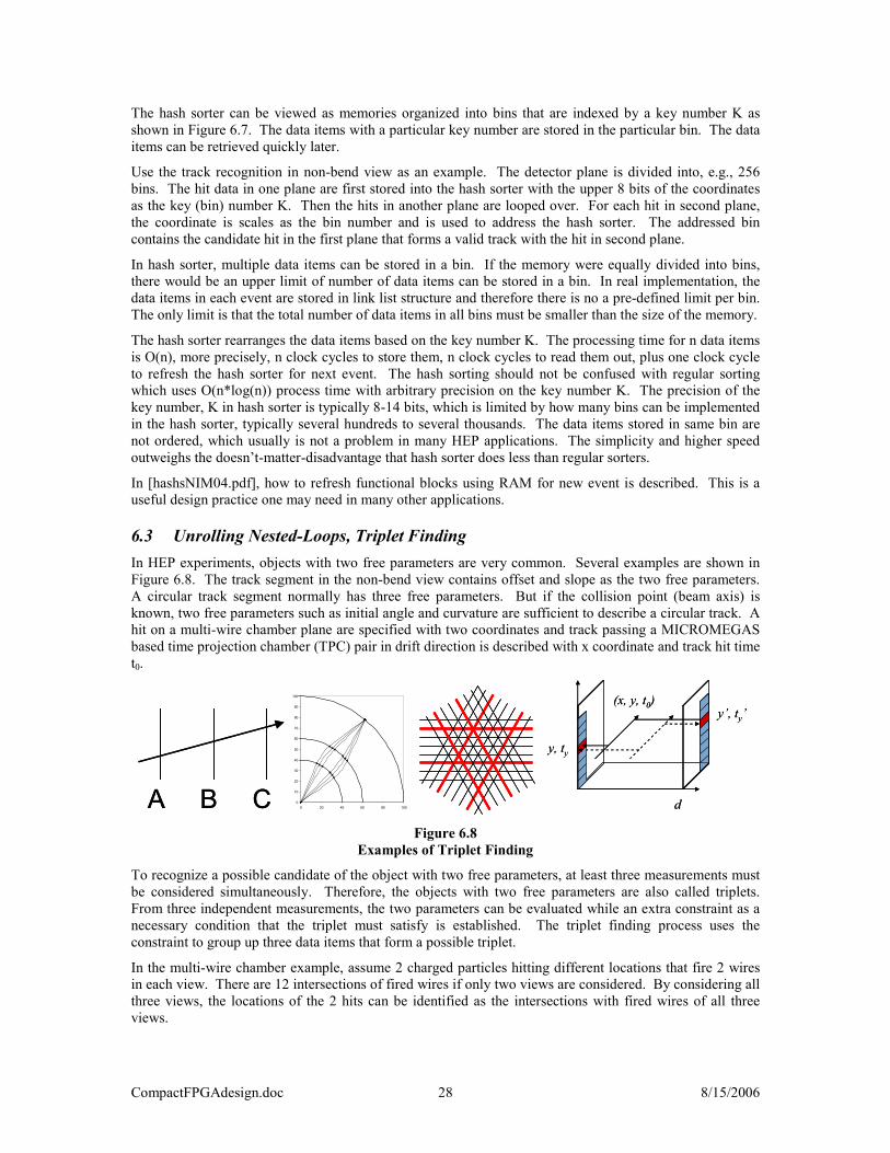
CompactFPGAdesign.doc 28 8/15/2006
The hash sorter can be viewed as memories organized into bins that are indexed by a key number K as shown in Figure 6.7. The data items with a particular key number are stored in the particular bin. The data items can be retrieved quickly later.
Use the track recognition in non-bend view as an example. The detector plane is divided into, e.g., 256 bins. The hit data in one plane are first stored into the hash sorter with the upper 8 bits of the coordinates as the key (bin) number K. Then the hits in another plane are looped over. For each hit in second plane, the coordinate is scales as the bin number and is used to address the hash sorter. The addressed bin contains the candidate hit in the first plane that forms a valid track with the hit in second plane.
In hash sorter, multiple data items can be stored in a bin. If the memory were equally divided into bins, there would be an upper limit of number of data items can be stored in a bin. In real implementation, the data items in each event are stored in link list structure and therefore there is no a pre-defined limit per bin. The only limit is that the total number of data items in all bins must be smaller than the size of the memory.
The hash sorter rearranges the data items based on the key number K. The processing time for n data items is O(n), more precisely, n clock cycles to store them, n clock cycles to read them out, plus one clock cycle to refresh the hash sorter for next event. The hash sorting should not be confused with regular sorting which uses O(n*log(n)) process time with arbitrary precision on the key number K. The precision of the key number, K in hash sorter is typically 8-14 bits, which is limited by how many bins can be implemented in the hash sorter, typically several hundreds to several thousands. The data items stored in same bin are not ordered, which usually is not a problem in many HEP applications. The simplicity and higher speed outweighs the doesn’t-matter-disadvantage that hash sorter does less than regular sorters.
In [hashsNIM04.pdf], how to refresh functional blocks using RAM for new event is described. This is a useful design practice one may need in many other applications.
6.3 Unrolling Nested-Loops, Triplet Finding In HEP experiments, objects with two free parameters are very common. Several examples are shown in Figure 6.8. The track segment in the non-bend view contains offset and slope as the two free parameters. A circular track segment normally has three free parameters. But if the collision point (beam axis) is known, two free parameters such as initial angle and curvature are sufficient to describe a circular track. A hit on a multi-wire chamber plane are specified with two coordinates and track passing a MICROMEGAS based time projection chamber (TPC) pair in drift direction is described with x coordinate and track hit time t0.
A B CA B C 0
10
20
30
40
50
60
70
80
90
100
0 20 40 60 80 100
y, ty
d
y’, ty’(x, y, t0)
y, ty
d
y’, ty’(x, y, t0)
Figure 6.8 Examples of Triplet Finding
To recognize a possible candidate of the object with two free parameters, at least three measurements must be considered simultaneously. Therefore, the objects with two free parameters are also called triplets. From three independent measurements, the two parameters can be evaluated while an extra constraint as a necessary condition that the triplet must satisfy is established. The triplet finding process uses the constraint to group up three data items that form a possible triplet.
In the multi-wire chamber example, assume 2 charged particles hitting different locations that fire 2 wires in each view. There are 12 intersections of fired wires if only two views are considered. By considering all three views, the locations of the 2 hits can be identified as the intersections with fired wires of all three views.

CompactFPGAdesign.doc 29 8/15/2006
In the MICROMEGAS TPC pair, the coordinate x and hit time t0 can be calculated if there is only one pulse within sufficient long time window in each of the two pads in opposite sides. If multiple pulses are generated by multiple tracks in a pad pair, without additional measurement, the pulses may be mismatched resulting in ghost hits. A possible additional measurement can be particle hit times, either derived from accelerator RF or measured from other detectors. The additional measurements can also be made with additional TPC with different drifting directions or different drifting velocities.
In software, triplet finding is implemented with three layers nested loops, assuming in an event, there are n1, n2 and n3 hits on the three detector planes: for(i1=0; i1<n1; i1++){ for(i2=0; i2<n2; i2++){ for(i3=0; i3<n3; i3++){ CheckCondition(y1[i1], y2[i2], y3[i3]); }
}}
The execution time of the process is O(n3) where n is number of hits on the three planes in an event.
In an online trigger system, the process time must cope with the data fetching time which is proportional to the number of hits on a detector plane, i.e., O(n). It is then necessary to reduce the execution time of the process by “unrolling” two layers of the nested loops.
Obviously it is possible to go though a doublet finding stage first and then find the triplets. However, there are methods to find triplet directly without constructing doublets. Several schemes are discussed below.
6.3.1 The Hough Transform
Consider the straight track segment finding problem in the non-bend view with the plane A and C being divided into N bins each. A bin can be a natural detector element, or a group of the elements. There are total N2 to 2N2 possible track configurations depending on how the plane B is divided. A valid track configuration is called a “road”.
The track segment is determined by two free parameters. The method of Hough transform is to book a multi-dimensional histogram in the parameter space. (The actual hits are in “image space”.) In our example, there are two free parameters so the histogram is 2-dimensional. A bin in the parameter space represents a set of parameters that corresponds a road. A hit in the image space may be a part of many possible roads which in general is a curve in the 2-D histogram. While processing an event, each hit causes a set of cells on the curve to increment by 1. The curves of hits from different detector planes intersect at common cells. After hits from all detector planes are processed, the peaks in the 2-D histogram represent the actual roads of the tracks. The method is illustrated in Figure 6.9.
A B CA B C yC
yA
yB=const.
yC
yA
yB=const.
Figure 6.9
Hough Transform for Triplet Finding
There are many choices of parameters and the coordinates of the hits on plane A and C can be chosen as the two parameters for convenience. The 2-D histogram contains N2 cells each can be visualized as a counter with count enable input.

CompactFPGAdesign.doc 30 8/15/2006
A hit in plane A represents a curve in the parameter space which is a horizontal straight line due to our choice of parameters. Each hit in the plane A enables a row of the counters so that they all increment by 1. Similarly, a plane C hit enables a column of the counters. A hit in the plane B represents a diagonal straight line and enables corresponding counters for incrementing. The intersection of three lines represents the roads of the track. The cell is accumulated to 3 while other cells are not. If there are more detector planes, the hits from different planes represent lines with different angles and they should all intersect at a common cell if they are created by the same charged particle track. The cell should have a count equals to the number of detector planes. With more than 3 planes, designer may use more flexible peak finding algorithm to accommodate detector inefficiency or boundary effect. For example, with 5 detector planes, a valid peak can be defined as a cell equals 4 or 5, allowing 1 missing hit.
The obvious drawback is the large O(N2) silicon usage of the 2-D histogram. Note that each bin or cell in the histogram contains a counter, count enable logic and peak recognition logic that consumes several logic elements in FPGA.
6.3.2 The Tiny Triplet Finder (TTF)
In many applications, constraint of the triplet is an invariant under shift, i.e., the constraint remain valid if all the measurements are added with a constant offset. In the straight track segment finding, multi-wire chamber and TPC examples, their constraints are linear so they are obviously invariants under shift. The constraint for circular track is not linear, but it remains valid under rotation, i.e., all measured azimuth angles can be added with a common offset. If the application satisfies the shift invariant condition, the tiny triplet finder (TTF) is a suitable scheme for triplet finding process. The circular track segment finding using TTF is shown in Figure 6.10.
0
10
20
30
40
50
60
70
80
90
100
0 20 40 60 80 100
*R1/R3
*R2/R3
Triplet Map Output To Decoder
Bit
Arra
y
Shifter
Bit
Arra
y
ShifterBit-wise Coincident Logic
*R1/R3
*R2/R3
Triplet Map Output To Decoder
Bit
Arra
y
Shifter
Bit
Arra
y
ShifterBit-wise Coincident Logic
Figure 6.10
The Tiny Triplet Finder
The key feature of TTF is its low O(N*logN) silicon resource usage. The TTF uses logarithmic shifters with silicon resource usage O(N*logN) to shift hit patterns before feeding to a bit-wise coincident logic so that the coincident logic is properly reused each clock cycle. The principle of TTF has been discussed in [TTF_lecc2004p-v3.pdf], [TTF_paper05_vMar06.pdf] and [TTFcurv_paper06.pdf].
6.4 Track Fitter In high-energy physics experiment detectors, track fitting is normally considered as a software task in the higher level trigger stage or analysis stage. Almost all relative decent fitting algorithms require floating point multiplications and divisions. Although direct porting the fitting algorithm into today’s large size FPGA is not impossible, the cost and power consumption quickly become concerns without careful resource usage control. In fact, many silicon area and power consuming operations like multiplications and divisions in many algorithms can be eliminated or replaced by low resource usage operations such as shifts, additions and subtractions. A process deviating from the mathematically accurate one certainly produces

CompactFPGAdesign.doc 31 8/15/2006
less perfect results. However, significant reduction in FPGA logic elements and power consumption overweighs small imperfectness.
In [TrkFit_paper06.pdf], a curved track fitting as shown in Figure 6.11 algorithm that needs only shifts, additions and subtractions is studied. It is modified from the least square fitting method and its fitting errors are only slightly increases from the mathematically perfect ones.
z=z0(z-z0)=-1 (z-z0)=+1 (z-z0)=+3(z-z0)=-3
2hy0
-4η
-η
z=z0(z-z0)=-1 (z-z0)=+1 (z-z0)=+3(z-z0)=-3
2hy0
-4η
-η
z=z0(z-z0)=-2 (z-z0)=+2 (z-z0)=+4(z-z0)=-4
4hy0
-4η
z=z0(z-z0)=-2 (z-z0)=+2 (z-z0)=+4(z-z0)=-4
4hy0
-4η
Figure 6.11 The Curved Track Fitting
The 5 track parameters (two offsets, two slopes at middle of the track and curvature in the bend view) of a track are found with the following linear combinations.
20
00
00
)(/
)(//
)(//
∑ ∑
∑∑∑∑
∑∑∑∑
−=
−==
−==
i iiiii
iii
iii
ii
iii
iii
iii
ii
iii
zzeye
zzdydhcycy
zzbxblaxax
η
Usually, floating point multiplication and divisions are needed. However, the coefficients in the linear combinations are modified from the least-squares fitting algorithm. Only “weigh-two” or “two-bit” integers are chosen as the coefficients. An example of choosing e[i], the coefficients for calculating parameter η guided by ei, the one derived from the least-squares algorithm is shown in Table 6-1.
Half-length of the Track
16 14 12 10 8 6 4z-z0 ei e[i] ei e[i] ei e[i] ei e[i] ei e[i] ei e[i] ei e[i]
-16 5.3 6-14 3.3 2 7.5 8-12 1.6 2 4.3 4 11.3 12-10 0.1 0 1.6 2 5.6 5 17.9 18
-8 -1.1 0 -0.7 -2 1.0 1 7.2 7 31.0 31-6 -2.0 -3 -2.4 -2 -2.6 -4 -1.2 -1 7.8 8 61.0 56-4 -2.6 -3 -3.6 -5 -5.1 -5 -7.2 -8 -8.9 -9 0.0 12 146.3 144-2 -3.0 -3 -4.4 -4 -6.6 -5 -10.7 -9 -18.8 -20 -36.6 -40 -73.1 -640 -3.2 -2 -4.6 -2 -7.2 -8 -11.9 -14 -22.2 -20 -48.8 -56 -146.3 -1602 -3.0 -3 -4.4 -4 -6.6 -5 -10.7 -9 -18.8 -20 -36.6 -40 -73.1 -644 -2.6 -3 -3.6 -5 -5.1 -5 -7.2 -8 -8.9 -9 0.0 12 146.3 1446 -2.0 -3 -2.4 -2 -2.6 -4 -1.2 -1 7.8 8 61.0 568 -1.1 0 -0.7 -2 1.0 1 7.2 7 31.0 31
10 0.1 0 1.6 2 5.6 5 17.9 1812 1.6 2 4.3 4 11.3 1214 3.3 2 7.5 816 5.3 6
Error 2.91 3.02 3.05 3.15 3.22 3.26 3.41 3.43 3.65 3.65 3.93 3.99 4.28 4.29Ratio 1.04 1.03 1.01 1.00 1.00 1.02 1.00
Table 6-1 The Coefficients of the FPGA Fitting Algorithm
Since the coefficients are simply two-bit integers, a multiplication of the coefficient is reduced to two shift and accumulation operations. Please read [TrkFit_paper06.pdf] for details.
Since the operations of algorithm are very simple, it can be implemented into an FPGA with very low silicon resource usage. The track fitting functional block calculates 5 parameters (two offsets, two slopes at middle of the track and curvature in the bend view) of a track while the coordinate data of the hits on the detector planes flow though. The tracks are allowed to have various numbers of hits so that the advantages

CompactFPGAdesign.doc 32 8/15/2006
of redundant measurements and long lever arm for tracks with more hits are fully taken. The fitting errors are only increased from the one of least-squares algorithm slightly (<4%).
It is often the case that in a computation problem, large percentage of arithmetic logic operations is spent to make the last a few percents of improvement. With some care, it is possible to eliminate those excessive operations without significantly degrading the final results.
7 Several Examples for FPGA Computation
7.1 Sliding Sum, Pedestal and RMS The sliding sum is a very useful variable in online systems. The sliding sum of an input stream represents an average in a short period of time. The input noise is smoothed out in the sliding sum. It can be viewed as a low pass filter. The pedestal and RMS of an input stream provide commonly used characterizations of the signal sequence. The block diagrams for calculations of the sliding sum, pedestal and RMS are shown in Figure 7.1.
ΣS
XA
(A-B)B
ΣS
XA
(A-B)B D Q
EN
A(A-B)
B
X
Σ
X X2
ΣSubσ2D Q
EN
A(A-B)
B
X
Σ
X X2
ΣSubσ2
Figure 7.1 Sliding Sum, Pedestal and RMS Calculations
To calculate the sliding sum, the input data are accumulated and the raw data are stored in a buffer organized as a fix length pipeline. When more data points than the sum length are accumulated, the output from the pipeline, i.e., the tail of the sequence, is subtracted each time when a new data is added.
At the start up when less data points than the sum length is input, the tail being subtracted should be zero. However, the contents in the memory buffer may not be zero since block memories usually can not be reset through a global command. One may certainly initialize the buffer by writing zeros into it but the process takes long time. A better way is to use an AND gate at the data path of the tail. The AND gate first suppresses the tail to zero before number of input data points is reaching the pre-defined sum length. Then the AND gate let the tail data though.
The mean and the standard deviation (squared) of the input stream can be written:
2
1
0
1
0
2
222
1
0 )(N
x
N
xxx
N
xx
N
ii
N
ii
N
ii ∑∑∑
−
=
−
=
−
= −=−== σ
It is convenient to choose N = 2m, i.e., 256, 512, 1024 etc. so that the division can be simply implemented as bit shift. In fact, the “shift” operation in FPGA usually is just choosing corresponding bits while feeding the data to later stage and consumes no real silicon resource.
The circuit of calculating standard deviation uses two accumulators, one to accumulate the raw input data the other to accumulate square of each input data. After N data points are accumulated, the bits of sum of input data are chosen for division to produce the mean. The mean is then squared and subtracted (with appropriate bit alignment) from the accumulator result that represents the sum of squared input data. After the process, the squared standard deviation σ2 is presented at the output.
To find σ itself, a square root operation can be performed. Perhaps the simplest method for finding square root is to use a lookup table.
Sometimes the pedestal is relatively large comparing the dynamic range of the noise. For example, in Fermilab BLM system, the pedestal of the ADC input is typically 700 counts while the noise is only 2-3

CompactFPGAdesign.doc 33 8/15/2006
counts up and down from the pedestal. If the input is squared directly, an input of 10 bits or more would be needed and the result becomes 20 bits or more. The silicon resource usage of the square operation block with K bits is O(K2) if the square function is implemented with a multiplier, and is O(K2K) if implemented using lookup table. It is known that the standard deviation remains the same if all inputs are subtracted with a common offset. So in the circuit shown above, the first input data point is chosen to be the offset and all the remaining input are subtracted with the offset. The difference stream then contains data with relatively small absolute values and its dynamic range becomes only 3-4 bits.
Another point should be mentioned here is that the square operation functional block is reused for both calculating xi
2 during the accumulation and calculating the square of the mean after the accumulation is done. The square functional block consumes relatively big silicon resource so it is good idea to reuse it as much as possible.
7.2 Center of Gravity Method of Pulse Time Calculation In detectors like calorimeters, particle hits sometimes generate relatively wide pulses and the ADC is able to sample the pulse to record multiple data points. It is often necessary to determine the arrival time so that the pulse can be tagged with certain event. The sampling period of the ADC is normally several times bigger than the required precision of pulse arrival time estimation. For example, the sampling period of a 40 MHz ADC is 25 ns while the required precision of the arrival time can be 2-3 ns. Time determined by traditional over-threshold discrimination scheme varies depending on the pulse height and noise. A typical pulse with noise is shown in Figure 7.2.
-20
0
20
40
60
80
100
120
0 10 20 30 40 50 60 70
Figure 7.2
The Simulated Pulse with Noise
There are many algorithms for pulse arrival time determination that all take advantage of statistical properties of multiple measurements to eliminate effects of noise and pulse height. A simplest one that can be implemented in FPGA with low resource usage is the center of gravity scheme as shown in Figure 7.3.
The center of gravity of an input stream x j is defined as:
∑∑−
=
−
=
⋅=1
0
1
0
N
jj
N
jj xxjt
It is a ratio of the sum of input sequence and the sum of the input sequence weighted by the sampling time. Clearly the pulse height is canceled and the random noise can be averaged to a relatively lower level in the sums of multiple data points. (Maybe, a pedestal is to be subtracted from the input stream first.)

CompactFPGAdesign.doc 34 8/15/2006
A(A*B)
B
X
Σ
Σ A(A/B)
B
Counterj
t
A(A*B)
B
X
Σ
Σ A(A/B)
B
Counterj
t
0
0.125
0.25
0.375
0.5
0.625
0.75
0.875
1
0 0.125 0.25 0.375 0.5 0.625 0.75 0.875 1
Pulse Time Offset (Sampling Interval)
Fitte
dA
rriv
alTi
me
Ideal
Center of Gravity Method
Figure 7.3
Center of Gravity Method for Pulse Time Estimate
The simple scheme is able to estimate the pulse arrival time good to about 1/4 to 1/8 of the sampling time interval. The estimated time becomes available shortly after the accumulation of the input sequence covering the pulse is done, so it is good for online coarse event time estimate in trigger system.
The multiplier in the circuit can be replaced with a logarithmic shifter that uses lower silicon resource. There are usually a few clock cycles in FPGA for each input data sample since in general analog circuits in ADC can not be driven as fast as digital circuits in FPGA. For example, for each sample in a 40MHz ADC, there are 4 clock cycles to process each sample point in an FPGA running at 160MHz. One may take this advantage to use shift and accumulation to implement the multiplication. For example, an 8-bit multiplication can be done by adding or subtracting a number (and its shifted versions) 4 times into an accumulator.
The numerator and denominator for the divider in the last stage are the results of the accumulation of multiple points. So the divider has many clock cycles to do the division since the next numerator and denominator are to be accumulated over long time. A sequential divider is preferred due to its compact size to the single-step divider that uses large logic element resource.
7.3 Lookup Table Usage The lookup table is a convenient means of implementing functions. The lookup table is a block memory, usually organized as a ROM. The variable of the function is input as the address and the pre-stored content at the address in the ROM is output as the function value.
As pointed out before, the silicon resource usage of a lookup table with K bits is O(K2K) which is a very rapid raise. Based on this fact, the number of bits of the input variable should be limited. As of today, a reasonable width of the block memory address is around 8-12 bits in FPGA. If we trust Moore’s Law, that everything doubles every 18 months, there are still about 30 years to go before we can easily implement 32-bit lookup tables.
In principle, the functions implemented with lookup tables can be multi-variable ones. However, to share 8-12 bits among several variables results in poor precisions on each variable. So typically the lookup tables are used to implement single variable functions. In certain cases, for example, to find a ratio of two numbers with 4-5 bits precision, the division can be implemented with lookup table. Otherwise, to find Y/X, it is a common practice to use a lookup table to find 1/X first and then use a multiplier to find Y*(1/X). This way, the division with 8-12 bits precision can be performed at a rate of one operation per clock cycle.
7.4 The Enclosed Loop Micro-Sequencer (ELMS) The sequence control of the data processing resources is an important issue in FPGA design.

CompactFPGAdesign.doc 35 8/15/2006
Sequence control is normally implemented using either finite state machines (FSM) or embedded micro-processor cores. When an input data item is to be fed through a fast and very simple process, typically using a few clock cycles, FSM is a suitable means of sequence control. FSM also responds to external conditions promptly and accurately. However, the sequence or program in the FSM is not easy to change and debug, especially when irregularities exist in the sequence. Also, the state machines occupy logic elements no matter how rarely they are used. So it is not economical to use FSM to implement the occasionally-used sequences such as initialization, communication channel establishment, etc.
Embedded or external micro-processor is another option of sequence control. Today’s main stream micro-processors are ALU (Arithmetic Logic Unit) oriented. The ALU, being the center piece of the micro-processor, performs not only data processing, but also program control functions. The ALU oriented architectures have two drawbacks in FPGA computation. (1) When a micro-processor core is embedded in an FPGA, the ALU occupies large amount of silicon resources. In instances where the application specific data processing is implemented in dedicated logic for the sake of speed, the ALU is barely utilized. (2) The program loops are implemented using conditional branches, which are the primary source of the micro-complexity of pipeline bubble, branch penalty etc. that needs to be solved with further micro-complexities such as branch prediction. The micro-processor is a better choice only if a data item is to be processed with a very complicate program, typically using thousands of clock cycles.
ProgramCounter
ROM128x
36bits
Reset A
Con
trolS
igna
ls
CLK
ProgramCounter
ROM128x
36bits
Reset A
Con
trolS
igna
ls
CLK
ProgramCounter
ROM128x
36bits
A
Loop & Return Logic + Stack
Conditional Branch Logic
Reset
CLK Con
trolS
igna
ls
ProgramCounter
ROM128x
36bits
A
Loop & Return Logic + Stack
Conditional Branch Logic
Reset
CLK Con
trolS
igna
ls
Figure 7.4 The Micro-Sequencers
When a data item is to be processed with a medium length program, e.g., using a few hundreds clock cycles, the sequence control needed is not too much more than a PC+ROM structure (Figure 7.4, left), which is the starting point of the Enclosed Loop Micro-Sequencer (ELMS) (Figure 7.4, right). The primary difference between the ELMS and regular micro-processor is that in the ELMS there are no data processing resources like an ALU. The control signals for external data processing resources turn on and off according to the sequence stored in the ROM as the program counter (PC) increases. Obviously, supporting logic must be added to control the PC. In addition to the conditional branch logic that also exists in micro-processors, loop and return logic with an internal stack are added in the ELMS, so that it supports “FOR” loops with constant iterations at the machine code level and is self-sufficient to run multi-layer nested-loop programs.
Most of program loops in micro-processors are implemented with conditional branches that are the origin of many micro-complexities like branch prediction. Intrinsically, loops with pre-defined iterations need not use conditional branches. The ELMS supports the “FOR” loops with constant iterations at the machine code level, which provides programming convenience and avoids micro-complexities from the beginning. The ELMS is able to run multi-layer nested-loop programs without help from external arithmetic/logic resources used for data processing. Since the data processing resources are external and purely user defined, the ELMS is not a traditional micro-processor, which is why it is called a “micro-sequencer”. The ELMS is used in the digitizer FPGA for the Fermilab Beam Loss Monitor system with expected performances.
Please read [ELMS_paper06.pdf] for additional details.