cp2130 - farnell
TRANSCRIPT

CP2130
SINGLE-CHIP USB-TO-SPI BRIDGE
Single-Chip USB-to-SPI BridgeIntegrated clock; no external crystal requiredIntegrated USB transceiver; no external resistors
requiredIntegrated 348 Byte one-time programmable ROM for
product customizationOn-chip power-on reset circuitOn-chip voltage regulator: 3.45 V outputUses USB Bulk Mode transactions for high throughput
- Configurable priority for reads and writes
USB Peripheral Function ControllerUSB Specification 2.0 compliant; full-speed (12 Mbps)USB suspend states supported and indicated via
suspend output pins
USB Interface
Windows 8®, 7®, Vista®, and XP®
Open access to interface specification
Windows LibrariesAPIs for quick application development
Supports Windows 8®, 7®, Vista®, and XP® (SP2 & SP3)
PackagesRoHS-compliant 24-QFN package (4x4 mm)
SPI Controller3 or 4-wire master mode operationConfigurable clock rate
- 12 MHz, 6 MHz, 3 MHz, 1.5 MHz, 750 kHz, 375 kHz, 187.5 kHz, 93.75 kHz
Clock phase and polarity controlChip select mode and toggleProgrammable SPI delay (post-assert, inter-byte, pre-
deassert)
11 Configurable GPIO Pins with Alternate FunctionsUsable as inputs, open-drain outputs, or push-pull
outputsUp to 11 chip select outputsReady-to-read pin allows for external signal to trigger
SPI read operationsAbility to count edges or pulses using the Event CounterUp to 11 USB remote wakeup sourcesSPI activity indication (toggles to indicate SPI activity)Configurable clock output (93.75 kHz to 24 MHz)
Supply VoltageSelf powered (regulator disabled): 3.0 to 3.6 VSelf powered (regulator enabled): 3.0 to 5.25 VUSB bus powered: 4.0 to 5.25 VI/O voltage: 1.8 V to VDD
Ordering Part NumbersCP2130-F01-GM
Temperature Range: –40 to +85 °C
Figure 1. Example System Diagram
CP2130
48 MHz Oscillator
VBUS
D+
D-
GND
USB Connector
Logic Level Supply
(1.8 V to VDD)
Multi-Function Signals
USB Interface
Peripheral Function Controller
Full-Speed 12 Mbps
Transceiver
SCK
MISO
MOSI
VREGIN
VDD
GND
VIO
VBUS
D+
D-
I/O Power and Logic Levels
GPIO.6_CS6
GPIO.5_CS5_CLKOUT
Voltage Regulator SPI Controller
Connect to VBUS or External Supply
GPIO
VPP
To SPI Slave
Devices
Multi-Function Signals to External Circuitry
GPIO.0_CS0
GPIO.1_CS1
GPIO.2_CS2
GPIO.3_CS3_RTR
GPIO.4_CS4_EVTCNTR
348 Byte PROM(Product Customization)
GPIO.7_CS7
GPIO.8_CS8_SPIACT
GPIO.9_CS9_SUSPEND
GPIO.10_CS10_SUSPEND
Hardware Reset
SPI Chip Select
SPI Event Counter
Clock Output
USB Suspend
SPI Activity
SPI ReadyToRead
Remote Wakeup
RESET
Rev. 0.7 1/14 Copyright © 2014 by Silicon Laboratories CP2130This information applies to a product under development. Its characteristics and specifications are subject to change without notice.

CP2130
2 Rev. 0.7

CP2130
TABLE OF CONTENTS
Section Page
1. System Overview . . . . . . . . . . . . . . . . . . . . . . . . . . . . . . . . . . . . . . . . . . . . . . . . . . . . . . . . .42. Electrical Characteristics . . . . . . . . . . . . . . . . . . . . . . . . . . . . . . . . . . . . . . . . . . . . . . . . . .53. USB Function Controller and Transceiver . . . . . . . . . . . . . . . . . . . . . . . . . . . . . . . . . . . . .94. Serial Peripheral Interface (SPI) . . . . . . . . . . . . . . . . . . . . . . . . . . . . . . . . . . . . . . . . . . . .10
4.1. Signal Descriptions . . . . . . . . . . . . . . . . . . . . . . . . . . . . . . . . . . . . . . . . . . . . . . . . . .104.2. Data Throughput . . . . . . . . . . . . . . . . . . . . . . . . . . . . . . . . . . . . . . . . . . . . . . . . . . . .114.3. Serial Clock Phase and Polarity . . . . . . . . . . . . . . . . . . . . . . . . . . . . . . . . . . . . . . . .11
5. GPIO Pins . . . . . . . . . . . . . . . . . . . . . . . . . . . . . . . . . . . . . . . . . . . . . . . . . . . . . . . . . . . . . .145.1. GPIO.3—Ready-to-Read (RTR) . . . . . . . . . . . . . . . . . . . . . . . . . . . . . . . . . . . . . . . .155.2. GPIO.4—Event Counter . . . . . . . . . . . . . . . . . . . . . . . . . . . . . . . . . . . . . . . . . . . . . .155.3. GPIO.5—Clock Output . . . . . . . . . . . . . . . . . . . . . . . . . . . . . . . . . . . . . . . . . . . . . . .155.4. GPIO.8—SPI Activity Indicator . . . . . . . . . . . . . . . . . . . . . . . . . . . . . . . . . . . . . . . . .165.5. GPIO.9-10—SUSPEND and SUSPEND . . . . . . . . . . . . . . . . . . . . . . . . . . . . . . . . . .165.6. USB Remote Wakeup . . . . . . . . . . . . . . . . . . . . . . . . . . . . . . . . . . . . . . . . . . . . . . . .165.7. GPIO State During USB Suspend . . . . . . . . . . . . . . . . . . . . . . . . . . . . . . . . . . . . . . .16
6. One-Time Programmable ROM . . . . . . . . . . . . . . . . . . . . . . . . . . . . . . . . . . . . . . . . . . . . .177. Voltage Regulator . . . . . . . . . . . . . . . . . . . . . . . . . . . . . . . . . . . . . . . . . . . . . . . . . . . . . . . .188. CP2130 Interface Specification and Windows Interface DLL . . . . . . . . . . . . . . . . . . . . .209. Relevant Application Notes . . . . . . . . . . . . . . . . . . . . . . . . . . . . . . . . . . . . . . . . . . . . . . . .2010. Pin Descriptions . . . . . . . . . . . . . . . . . . . . . . . . . . . . . . . . . . . . . . . . . . . . . . . . . . . . . . . .2111. QFN-24 Package Specifications . . . . . . . . . . . . . . . . . . . . . . . . . . . . . . . . . . . . . . . . . . .2412. PCB Land Pattern . . . . . . . . . . . . . . . . . . . . . . . . . . . . . . . . . . . . . . . . . . . . . . . . . . . . . . .25Document Change List . . . . . . . . . . . . . . . . . . . . . . . . . . . . . . . . . . . . . . . . . . . . . . . . . . . . .26Contact Information . . . . . . . . . . . . . . . . . . . . . . . . . . . . . . . . . . . . . . . . . . . . . . . . . . . . . . . .27
Rev. 0.7 3

CP2130
1. System Overview
The CP2130 is a highly-integrated USB-to-SPI bridge controller providing a simple solution for bridging a UniversalSerial Bus (USB) host to a Serial Peripheral Interface (SPI) bus using a minimum of components and PCB space.The CP2130 includes a USB 2.0 full-speed controller, USB transceiver, oscillator, one-time programmable (OTP)ROM, and a SPI controller in a compact 4 x 4 mm QFN24 package (sometimes called “MLF” or “MLP”).
The on-chip, OTP ROM provides the option to customize the USB Vendor ID, Product ID, Manufacturer String,Product Description String, Power Descriptor, Device Release Number, Device Serial Number, and GPIOconfiguration as desired for OEM applications.
The CP2130 uses a Silicon Labs vendor-specific USB protocol using control and bulk transfers which is supportedby most operating systems through the use of generic USB drivers and interface libraries. A custom driver typicallydoes not need to be developed for this device. Windows applications communicate with the CP2130 through aWindows DLL which is provided by Silicon Labs that communicates with the Microsoft WinUSB driver via aWinUSB DLL. The interface specification for the CP2130 is also available to enable development of an API for anyoperating system that supports control and bulk transfers over USB.
The CP2130 SPI implements the standard signals, including SCK, MISO, MOSI, CS, as well as a ready-to-read(RTR) hardware handshaking input, so existing system firmware does not need to be modified. The SPIcapabilities of the CP2130 include fixed SPI clock rates ranging from 93.75 kHz to 12 MHz, configurable clockphase, configurable clock polarity, adjustable SPI delays, and up to 11 configurable chip select signals.
Any of the multi-purpose pins not used as chip select signals may instead be used as GPIO signals that are user-defined. The GPIO signals may also be configured to initiate a USB remote wakeup event on GPIO state change,which allows the CP2130 to wake a USB host from sleep mode. Eight of the GPIO signals support alternatefeatures including ready-to-read (RTR) handshaking, a configurable event counter, a configurable clock output(93.75 kHz to 24 MHz), SPI activity LED toggle, and USB suspend indicators. Support for I/O interface voltagesdown to 1.8 V is provided via a VIO pin.
An evaluation kit for the CP2130 (Part Number: CP2130EK) is available. It includes a CP2130-based USB-to-SPIevaluation board with SPI slave devices such as an EEPROM and ADC as well as connections for an externalCP2400 LCD controller EVB and SPI monitor. The kit also includes a Windows DLL and test application, USBcables, and full documentation. See www.silabs.com for the latest application notes and product supportinformation for the CP2130. Contact a Silicon Labs sales representatives or go to www.silabs.com to order theCP2130 Evaluation Kit.
4 Rev. 0.7

CP2130
2. Electrical Characteristics
Table 1. Global DC Electrical CharacteristicsVDD = 3.0 to 3.6 V, –40 to +85 °C unless otherwise specified.
Parameter Symbol Test Condition Min Typ Max Unit
Digital Supply Voltage VDD 3.0 — 3.6 V
Digital Port I/O Supply Voltage
VIO 1.8 — VDD V
Specified Operating Temperature Range
TA –40 — +85 °C
Thermal Resistance1 θJA — 28 — °C/W
Supply Current
USB Suspended2
IREGIN
Bus Powered; Regulator enabled — 170 360 µA
Self Powered; Regulator disabled; VDD = 3.0 V — 170 290 µA
Self Powered; Regulator disabled; VDD = 3.3 V — 210 330 µA
USB Normal; SPI Idle2
Bus Powered; Regulator enabled — 14.4 18.8 mA
Self Powered; Regulator disabled; VDD = 3.0 V — 13.8 18.1 mA
Self Powered; Regulator disabled; VDD = 3.3 V — 14.1 18.4 mA
USB Normal; SPI Active2
Bus Powered; Regulator enabled — 17.8 23.2 mA
Self Powered; Regulator disabled; VDD = 3.0 V — 16.6 21.7 mA
Self Powered; Regulator disabled; VDD = 3.3 V — 17.1 22.2 mA
USB Pull-up3 IPU — 200 230 µA
Notes:1. Thermal resistance assumes a multi-layer PCB with any exposed pad soldered to a PCB pad.2. USB Pull-up current should be added for total supply current. USB normal and suspended supply current is current
flowing into VREGIN. USB normal and suspended supply current is guaranteed by characterization.3. The USB Pull-up supply current values are calculated values based on USB specifications. USB Pull-up supply current
is current flowing from VDD to GND through USB pull-down/pull-up resistors on D+ and D-.
Rev. 0.7 5

CP2130
Table 2. SPI, Port I/O, and Suspend I/O DC Electrical CharacteristicsVIO = 1.8 to 3.6 V, –40 to +85 °C unless otherwise specified.
Parameters Symbol Test Condition Min Typ Max Unit
Output High Voltage VOH IOH = –10 µA, Port I/O push-pullIOH = –3 mA, Port I/O push-pull
IOH = –10 mA, Port I/O push-pull
VIO – 0.1VIO – 0.2
—
——
VIO – 0.4
———
V
Output Low Voltage VOL IOL = 10 µAIOL = 8.5 mAIOL = 25 mA
———
——0.6
0.10.4—
V
Input High Voltage VIH 0.7 x VIO — — V
Input Low Voltage VIL — — 0.6 V
Input Leakage Current IL Weak Pull-Up On, VIN = 0 V — 25 50 µA
Maximum Input Voltage Open drain, logic high (1) — — 5.8 V
Table 3. Reset Electrical Characteristics–40 to +85 °C unless otherwise specified.
Parameter Symbol Test Condition Min Typ Max Unit
VDD Ramp Time tRMP Time to VDD ≥ 2.7 V — — 1 ms
RST Input High Voltage VIHRESET 0.75 x VIO — — V
RST Input Low Voltage VILRESET — — 0.6 V
RST Low Time to Generate a System Reset
tRSTL 15 — — µs
Table 4. Voltage Regulator Electrical Specifications–40 to +85 °C unless otherwise specified.
Parameter Symbol Test Condition Min Typ Max Unit
Input Voltage Range1 VREGIN Regulator Enabled VDD + VDO — 5.25 V
Output Voltage2 VDDOUT Output Current = 1 to 100 mA 3.3 3.45 3.6 V
VBUS Detection Input Threshold
VBUSTH 2.5 — — V
Dropout Voltage VDO 1 mA ≤ IDD ≤ 100 mA — 1 — mV / mA
Bias Current — — 120 µA
Notes:1. Input range specified for regulation. When the internal regulator is not used, should be tied to VDD.2. The maximum regulator supply current is 100 mA. This includes the supply current of the CP2130.
6 Rev. 0.7

CP2130
Table 5. GPIO Output Specifications–40 to +85 °C unless otherwise specified.
Parameter Symbol Test Condition Min Typ Max Unit
GPIO.5 Clock Output* FCLKOUT FCLKOUT = configured frequency
FCLKOUT x 0.985
FCLKOUT FCLKOUT x 1.015
Hz
SPI Activity Toggle Rate FSPIACT — 10 — Hz
*Note: The clock output frequency is configurable from 93.75 kHz to 24 MHz.
Table 6. USB Transceiver Electrical Characteristics*VDD = 3.0 V to 3.6 V, –40 to +85 °C unless otherwise specified.
Parameter Symbol Test Condition Min Typ Max Unit
Transmitter
Output High Voltage VOH 2.8 — — V
Output Low Voltage VOL — — 0.8 V
Output Crossover Point VCRS 1.3 — 2.0 V
Output Impedance ZDRV Driving HighDriving Low
——
3636
——
Pull-up Resistance RPU Full Speed (D+ Pull-up) 1.425 1.5 1.575 k
Output Rise Time TR Full Speed 4 — 20 ns
Output Fall Time TF Full Speed 4 — 20 ns
Receiver
Differential Input Sensitivity VDI | (D+) - (D-) | 0.2 — — V
Differential Input Common Mode Range
VCM 0.8 — 2.5 V
Input Leakage Current IL Pullups Disabled — <1.0 — µA
*Note: Refer to the USB Specification for timing diagrams and symbol definitions.
Table 7. OTP ROM Electrical Characteristics–40 to +85 °C unless otherwise specified.
Parameter Symbol Test Condition Min Typ Max Unit
Digital Port I/O Supply VoltageDuring Programming
VIO 3.3 — VDD V
Voltage on VPP with respect to GND during aprogramming operation
VPP VIO > 3.3 V 5.75 — VIO + 3.6
V
Capacitor on VPP for In-system Programming — 4.7 — µF
Rev. 0.7 7

CP2130
Table 8. Thermal Characteristics
Parameter Symbol Min Typ Max Unit
Thermal Resistance* θJA — 28 — °C/W
*Note: Thermal resistance assumes a multi-layer PCB with any exposed pad soldered to a PCB pad.
Table 9. Absolute Maximum Ratings*
Parameter Symbol Test Condition Min Typ Max Unit
Ambient Temperature under Bias TBIAS –55 — 125 °C
Storage Temperature TSTG –65 — 150 °C
Voltage on RST, GPIO, or SPI Pins with respect to GND
VIO > 2.2 VVIO < 2.2 V
–0.3–0.3
——
5.8VIO + 3.6
V
Voltage on VBUS with respect to GND VBUS VDD > 3.0 VVDD not powered
–0.3–0.3
——
5.8VDD + 3.6
V
Voltage on VDD or VIO with respect to GND VDD –0.3 — 4.2 V
Maximum Total Current through VDD, VIO, REGIN, and GND
— — 500 mA
Maximum Output Current Sunk by RST or any I/O pin
— — 100 mA
*Note: Stresses above those listed may cause permanent damage to the device. This is a stress rating only, and functional operation of the devices at or exceeding the conditions in the operation listings of this specification is not implied. Exposure to maximum rating conditions for extended periods may affect device reliability.
8 Rev. 0.7

CP2130
3. USB Function Controller and Transceiver
The Universal Serial Bus (USB) function controller in the CP2130 is a USB 2.0-compliant, full-speed device withintegrated transceiver and on-chip matching and pullup resistors. The USB function controller manages all datatransfers between the USB and the SPI bus as well as command requests generated by the USB host andcommands for controlling the function of the SPI and GPIO pins.
The USB Suspend and Resume modes are supported for power management of both the CP2130 device as wellas external circuitry. The CP2130 enters Suspend mode when Suspend signaling is detected on the bus. Uponentering Suspend mode, the Suspend signals are asserted. The Suspend signals are also asserted after a CP2130reset until device configuration and USB Enumeration is complete. SUSPEND is logic high when the device is inthe Suspend state, and logic low when the device is in normal mode. The SUSPEND pin has the opposite logicvalue of the SUSPEND pin.
The CP2130 exits Suspend mode when any of the following occur: Resume signaling is detected or generated, aUSB Reset signal is detected, the configured GPIO wakeup sources do not match the configured latch value, or adevice reset occurs. SUSPEND and SUSPEND are weakly pulled to VIO in a high impedance state during aCP2130 reset. If this behavior is undesirable, a strong pulldown (10 k) can be used to ensure SUSPEND remainslow during reset.
The CP2130 can be configured to use any of the GPIO pins as a remote wakeup source. While suspended, if anyof the pins configured as a wakeup source does not match the configured wakeup match value, then the CP2130will send remote wakeup signaling to the USB host. If the host has configured the CP2130 to enable remotewakeup, then the host will send resume signaling to the CP2130 and the device will exit Suspend mode.
The logic level and output mode (push-pull or open-drain) of various pins during USB Suspend is configurable inthe OTP ROM. See Section 6 for more information.
Rev. 0.7 9

CP2130
4. Serial Peripheral Interface (SPI)
The CP2130 Serial Peripheral Interface (SPI) provides access to a flexible, full-duplex synchronous serial bus. TheCP2130 can operate as a master device in both 3-wire or 4-wire modes, and supports multiple slaves. Any of the11 GPIO pins may be configured as chip select master outputs to select multiple SPI slave devices.
4.1. Signal DescriptionsThe four signals used by SPI (MOSI, MISO, SCK, CS) are described below.
4.1.1. Master Out, Slave In (MOSI)
The master-out, slave-in (MOSI) signal is an output from a master device and an input to slave devices. It is usedto serially transfer data from the master to the slave. Data is transferred most-significant bit first.
4.1.2. Master In, Slave Out (MISO)
The master-in, slave-out (MISO) signal is an output from a slave device and an input to the master device. It isused to serially transfer data from the slave to the master. Data is transferred most-significant bit first.
4.1.3. Serial Clock (SCK)
The serial clock (SCK) signal is an output from the master device and an input to slave devices. It is used tosynchronize the transfer of data between the master and slave on the MOSI and MISO lines. Since the CP2130always acts as a SPI master, it always drives SCK.
4.1.4. Chip Select (CS0 - CS10)
The CP2130 may be used to control up to 11 different SPI slave devices using GPIO pins configured in chip selectoutput mode. Chip select signals are active low.
See Figure 2 and Figure 3 for typical connection diagrams of the various operational modes.
Figure 2. 3-Wire Single Master and 3-Wire Single Slave Mode Connection Diagram
Figure 3. 4-Wire Single Master Mode and 4-Wire Slave Mode Connection Diagram
Master Device
MISO
MOSI
SCK
Slave Device
MISO
MOSI
SCK
Master Device
MISO
MOSI
SCK
Slave Device
MISO
MOSI
SCK
Slave Device
MISO
MOSI
SCK
CS
CS
CS1
CS0
10 Rev. 0.7

CP2130
4.2. Data ThroughputSPI read and write data transfer throughput can be affected by many factors including USB host performance, hostdriver and PC application performance, SPI clock rate, and data transfer size. Also USB bulk transfers are limitedby available bandwidth on the bus; increased traffic on the bus may decrease SPI throughput. Additionally, theCP2130 can be configured to operate in high-priority write or high-priority read mode. The priority mode isconfigured in the OTP ROM. The CP2130 has two independent USB endpoints used for bulk data transfers. Thefirst endpoint is double buffered whereas the second endpoint is single buffered. Each endpoint is used for only asingle direction. A USB IN transfer is data transferred from the device to the host. A USB OUT transfer is datatransferred from the host to the device. More information about the USB interface can be found in application note,“AN792: CP2130 Interface Specification”. By default, the CP2130 is configured in high-priority write mode, in whichthe double-buffered endpoint is used for OUT transfers and the single-buffered endpoint is used for IN transfers.Conversely, when the CP2130 is configured in high-priority read mode, the double-buffered endpoint is used for INtransfers and the single-buffered endpoint is used for OUT transfers.Table 10 below shows the CP2130 typical SPI throughput in high-priority write and high-priority read modes usinga 64-bit PC.
4.3. Serial Clock Phase and PolarityFour combinations of serial clock phase and polarity can be selected using SPI control commands over the USBinterface. The clock phase (CPHA) specifies which clock edge is used to latch the data. The clock polarity (CPOL)selects between an active-high or active-low clock. Both master and slave devices must be configured to use thesame clock phase and polarity. The clock and data line relationships are shown in Figure 4.
The SPI clock field of the SPI control command controls the master mode serial clock frequency. The clockfrequency is restricted to discrete values between 93.8 kHz and 12 MHz.
Figure 4. Data/Clock Timing
Table 10. Typical SPI Throughput
Device Configuration Conditions WriteThroughput
ReadThroughput
WriteReadThroughput
Units
High-Priority Write Mode FSCK = 12 MHz;Block Size = 64 KB
4.9 4.6 3.5 Mbps
High-Priority Read Mode 4.2 6.6 2.9 Mbps
SCK(CPHA=Leading Edge, CPOL=Active High)
SCK(CPHA=Trailing Edge, CPOL=Active High)
SCK(CPHA=Leading Edge, CPOL=Active Low)
SCK(CPHA=Trailing Edge, CPOL=Active Low)
MSB Bit 6 Bit 5 Bit 4 Bit 3 Bit 2 Bit 1 Bit 0MISO/MOSI
Rev. 0.7 11

CP2130
Figure 5. SPI Master Timing (CPHA=Leading Edge)
Figure 6. SPI Master Timing (CPHA=Trailing Edge)
SCK*
MOSI
MISO
* SCK is shown for CPOL = Active High. SCK is the opposite polarity for CPOL = Active Low.
TMIHTMIS
SCK Shift Edge
1 / FSCK
SCK*
MISO
MOSI
* SCK is shown for CPOL = Active High. SCK is the opposite polarity for CPOL = Active Low.
TMISTMIH
SCK Shift Edge
12 Rev. 0.7

CP2130
Figure 7. SPI Delays (CPHA = Leading Edge)
Figure 8. SPI Delays (CPHA = Trailing Edge)
Table 11. SPI Timing Parameters1
Parameter Symbol Min Typ Max Units
SCK Frequency FSCK
12 MHz6 MHz3 MHz
1.5 MHz750 kHz375 kHz
187.5 kHz93.75 kHz
MISO Valid to SCK Shift Edge TMIS41.15 — — ns
SCK Shift Edge to MISO Change TMIH0 — — ns
Post-Assert SPI Delay2TPOST-ASSERT
N x 10 µs
Inter-Byte SPI Delay2TINTER-BYTE
N x 10 µs
Pre-Deassert SPI Delay2TPRE-DEASSERT
N x 10 µs
Notes:1. See Figures 5–8.2. N = user-specified delay values, where {0 ≤ N ≤ 65535}.
SCK*
MISO/MOSI
* SCK is shown for CPOL = Active High. SCK is the opposite polarity for CPOL = Active Low.
CS
TINTER‐BYTE DELAY
TPOST‐ASSERT TPRE‐DEASSERT
MSB LSB MSB LSB
SCK*
MISO/MOSI
* SCK is shown for CPOL = Active High. SCK is the opposite polarity for CPOL = Active Low.
CS
TINTER‐BYTE DELAY
TPOST‐ASSERT TPRE‐DEASSERT
MSB LSB MSB LSB
Rev. 0.7 13

CP2130
5. GPIO Pins
The CP2130 supports 11 user-configurable GPIO pins. Each of these GPIO pins are usable as inputs, open-drainoutputs, or push-pull outputs. Each GPIO pin may also be configured for use as SPI chip select signals for up to 11different SPI slaves. Six of these GPIO pins also have alternate functions which are listed in Table 12. Moreinformation regarding the configuration and usage of these pins is available in application note, “AN721: CP21xxCustomization Guide” available on the Silicon Labs website.
The default configuration for all of the GPIO pins is provided in Table 13. The configuration of the pins is one-timeprogrammable for each device. See Section 6 for more information about programming the GPIO pin functionality.
The difference between an open-drain output and a push-pull output is evident when the GPIO output is driven tologic high. A logic high, open-drain output pulls the pin to the VIO rail through an internal, pull-up resistor. A logichigh, push-pull output directly drives the pin to the VIO voltage. Open-drain outputs are typically used wheninterfacing to logic at a higher voltage than the VIO pin. These pins can be safely pulled to the higher, externalvoltage through an external pull-up resistor. The maximum external pull-up voltage is 5 V.
The speed of reading and writing the GPIO pins is subject to the timing of the USB interface and host computer.GPIO pins configured as inputs or outputs are not recommended for real-time signaling.
The following paragraphs describe the alternate functions available on the corresponding GPIO pin.
Table 12. GPIO Pin Alternate Functions
GPIO Pin Alternate Function
GPIO.3 Ready-to-Read (RTR)
GPIO.4 Event Counter
GPIO.5 Clock Output
GPIO.8 SPI Activity
GPIO.9 SUSPEND
GPIO.10 SUSPEND
Table 13. GPIO Pin Default Configuration
GPIO Pin Default Function GPIO Pin Default Function
GPIO.0 CS0 (Push-Pull Output) GPIO.6 GPIO (Input)
GPIO.1 CS1 (Push-Pull Output) GPIO.7 GPIO (Push-Pull Output)
GPIO.2 CS2 (Push-Pull Output) GPIO.8 SPI Activity (Push-Pull Output)
GPIO.3 RTR Active Low (Input) GPIO.9 SUSPEND (Push-Pull Output)
GPIO.4 Event Counter Rising Edge (Input) GPIO.10 SUSPEND (Push-Pull Output)
GPIO.5 Clock Output (Push-Pull Output)
14 Rev. 0.7

CP2130
5.1. GPIO.3—Ready-to-Read (RTR)RTR, or Ready-to-Read, is a configurable active-low or active-high input to the CP2130 and is used by the SPIslave device to indicate to the CP2130 when to read. When performing a Read with RTR command, the CP2130will only read SPI data when the RTR pin is asserted.
By default, GPIO.3 is configured to operate as the RTR input pin. In addition to the GPIO OTP ROM configuration,the device must be configured to use RTR flow control to use this pin.
Figure 9. Hardware Flow Control Typical Connection Diagram
5.2. GPIO.4—Event CounterGPIO.4 is configurable as an event counter digital input pin. The event counter can be configured to count edges orpulses. The four configurable modes are: rising edge, falling edge, positive pulse, or negative pulse. Onceconfigured for event counter mode, the CP2130 maintains a 16-bit counter that increments by ‘1’ whenever thespecified edge or pulse is detected. The user may query the CP2130 to get the current event count. The eventcounter can be used to detect slave interrupt events by connecting the slave interrupt output pin to the CP2130event counter pin.
5.3. GPIO.5—Clock OutputGPIO.5 is configurable to output a configurable CMOS clock output. The clock output appears at the pin at thesame time the device completes enumeration and exits USB Suspend mode. The clock output is removed from thepin when the device enters USB Suspend mode. The output frequency is configurable through the use of a dividerand the accuracy is specified in Table 5. When the divider is set to 0, the output frequency is 93.75 kHz. For dividervalues between 1 and 255, the output frequency is determined by the formula:
Equation 1. GPIO.0 Clock Output Frequency
Master Device Slave Device
RTR RTR
SCK SCK
MOSI MOSI
MISO MISO
GPIO.5 Clock Frequency24 MHzDivider---------------------=
Rev. 0.7 15

CP2130
5.4. GPIO.8—SPI Activity IndicatorGPIO.8 is configurable as a SPI activity indicator pin. This pin is logic high when a device is not transferring dataover the SPI, and toggles at a fixed rate as specified in Table 5 when a data transfer is in progress. Typically, thispin is connected to an LED to indicate data transfer.
Figure 10. SPI Activity Toggle Typical Connection Diagram
5.5. GPIO.9-10—SUSPEND and SUSPENDGPIO.9 and GPIO.10 are configurable as active-high SUSPEND and active-low SUSPEND pins. The SUSPENDpin is logic high when the device is in the suspended state and logic low when the device is in the active mode. TheSUSPEND pin has the opposite logic value of the SUSPEND pin.
5.6. USB Remote WakeupAny of the GPIO pins may be used to trigger a USB remote wakeup event. Before the CP2130 enters the Suspendstate, the device may be configured to wakeup on a port mismatch event. When any of the pins specified in thewakeup mask do not match the pin logic value specified in the wakeup value, the CP2130 will wakeup and signalremote wakeup on the bus. The CP2130 will assert USB remote wakeup signaling for 10 to 15 ms before the hostmay respond by resuming the CP2130.
Any GPIO pin used for remote wakeup must be configured as an input during the Suspend state. GPIO pins areselected as wakeup pins using the Wakeup Match Mask. The Wakeup Match Value specifies the logic level of thewakeup pin. When the pin level does not match the value specified, the device will wakeup. The default WakeupMatch Mask and Wakeup Match Value are shown in Table 15.
5.7. GPIO State During USB SuspendAll GPIO pins support programmable suspend state mode and latch values. When the CP2130 enter USBSuspend mode and the Use Suspend Mode and Values option is set, the CP2130 will reconfigure the GPIO pinsjust prior to entering USB Suspend mode. When the CP2130 resumes from USB Suspend mode, the GPIO pinsrevert to the previous function configurations and modes.
GPIO.8 – SPI Activity
CP2130
VIO
16 Rev. 0.7

CP2130
6. One-Time Programmable ROM
The CP2130 includes an internal, OTP ROM that may be used to customize the USB Vendor ID (VID), Product ID(PID), Manufacturer String, Product Description String, Power Descriptor, Device Release Number, Device SerialNumber, GPIO configuration, Suspend Pins and Modes as desired for OEM applications. If the OTP ROM has notbeen customized, the default configuration data shown in Table 14 and Table 15 is used.
While customization of the USB configuration data is optional, customizing the VID/PID combination is stronglyrecommended. A unique VID/PID will prevent the device from being recognized by any other manufacturer’ssoftware application. A vendor ID can be obtained from www.usb.org or Silicon Labs can provide a free PID for theOEM product that can be used with the Silicon Labs VID at www.silabs.com/RequestPID. All CP2130 devices arepre-programmed with a unique serial number. It is important to have a unique serial string if it is possible formultiple CP2130 devices to be connected to the same PC.
Application note, “AN792: CP2130 Interface Specification”, includes more information about the programmablevalues and their valid options. Note that certain items in the OTP ROM are programmed as a group andprogramming one of the items in the group prevents further programming of any of the other items in the group.
The configuration data OTP ROM is programmable by Silicon Labs prior to shipment with the desired configurationinformation. It can also be programmed in-system over the USB interface if a 4.7 µF capacitor is connectedbetween the VPP pin and ground. No other circuitry should be connected to VPP during a programming operation,and VIO must remain at 3.3 V or higher to successfully write to the configuration OTP ROM.
Table 14. Default USB Configuration Data
Name Value
Vendor ID 0x10C4
Product ID 0x87A0
Power Descriptor (Attributes) 0x80 (Bus-powered)
Power Descriptor (Max. Power) 0x32 (100 mA)
Release Number 0x0100 (Release Version 01.00)
Transfer Priority High Priority Write
Manufacturer String “Silicon Laboratories” (62 ASCII characters maximum)
Product Description String “CP2130 USB-to-SPI Bridge” (62 ASCII characters maximum)
Serial String Unique 8 character ASCII string (30 ASCII characters maximum)
Table 15. Default GPIO, UART, and Suspend Configuration Data
Name Value Name Value
GPIO.0 CS0 push-pull output Use Suspend Mode and Values
False
GPIO.1 CS1 push-pull output Suspend Mode 0x0000 (open-drain)
GPIO.2 CS2 push-pull output Suspend Latch 0x0000 (logic low)
GPIO.3 RTR active low Wakeup Match Mask 0x0000 (ignore all)
GPIO.4 Event counter rising edge Wakeup Match Value 0x0000 (match value logic low)
GPIO.5 Clock output Clock Divider 0 (93.75 kHz)
GPIO.6 GPIO input
GPIO.7 GPIO push-pull output
GPIO.8 SPI activity push-pull output
GPIO.9 SUSPEND push-pull output
GPIO.10 SUSPEND push-pull output
Rev. 0.7 17

CP2130
7. Voltage Regulator
The CP2130 includes an on-chip 5 V to 3.45 V voltage regulator. This allows the CP2130 to be configured as eithera USB bus-powered device or a USB self-powered device. A typical connection diagram of the device in a bus-powered application using the regulator is shown in Figure 11. When enabled, the voltage regulator output appearson the VDD pin and can be used to power external devices. See Table 4 for the voltage regulator electricalcharacteristics.
Note: By default, the CP2130 is configured for bus-powered operation. The CP2130 OTP configuration must be changed if thedevice will be operated in either of the self-powered modes.
If the regulator is used to provide VDD in a self-powered application, use the same connections from Figure 11, butconnect REGIN to an on-board 5 V supply, and disconnect it from the VBUS pin. In addition, if REGIN may beunpowered while VBUS is 5 V, a resistor divider (or functionally equivalent circuit) shown in Note 6 of Figure 12 isrequired to meet the absolute maximum voltage on VBUS specification in Table 9.
Figure 11. Typical Bus-Powered Connection Diagram
Note 4
SuspendSignals
SPIand
GPIOSignals
CP2130
MOSI
MISO
VPP
SUSPENDSUSPEND
VBUS
D+
D-
RST
VIO
4.7 kohm
Note 5
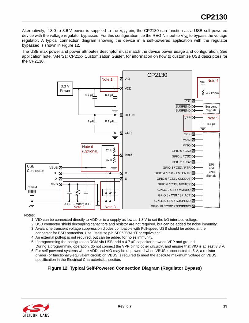
Notes: 1. VIO can be connected directly to VDD or to a supply as low as 1.8 V to set the I/O interface voltage. 2. USB connector shield decoupling capacitors and resistor are not required, but can be added for noise immunity. 3. Avalanche transient voltage suppression diodes compatible with Full-speed USB should be added at the connector for ESD protection. Use Littelfuse p/n SP0503BAHT or equivalent. 4. An external pull-up is not required, but can be added for noise immunity. 5. If programming the configuration ROM via USB, add a 4.7 F capacitor between VPP and ground. During a programming operation, do not connect the VPP pin to other circuitry, and ensure that VIO is at least 3.3 V.
4.7 F
Note 1
REGIN
VDD
GND
VIO
4.7 F 0.1 F
3.45 V Power
1 F 0.1 F
SCK
0.1 F0.1 F 1 MohmNote 3Note 2
VBUS
D+
D-
GND
USB Connector
Shield
GPIO.0 / CS0
GPIO.1 / CS1
GPIO.2 / CS2
GPIO.3 / CS3 / RTR
GPIO.4 / CS4 / EVTCNTR
GPIO.5 / CS5 / CLKOUT
GPIO.6 / CS6
GPIO.7 / CS7
GPIO.8 / CS8 / SPIACT
GPIO.9 / CS9 / SUSPEND
GPIO.10 / CS10 / SUSPEND
18 Rev. 0.7
CP2130
Alternatively, if 3.0 to 3.6 V power is supplied to the VDD pin, the CP2130 can function as a USB self-powereddevice with the voltage regulator bypassed. For this configuration, tie the REGIN input to VDD to bypass the voltageregulator. A typical connection diagram showing the device in a self-powered application with the regulatorbypassed is shown in Figure 12.
The USB max power and power attributes descriptor must match the device power usage and configuration. Seeapplication note, “AN721: CP21xx Customization Guide”, for information on how to customize USB descriptors forthe CP2130.
Figure 12. Typical Self-Powered Connection Diagram (Regulator Bypass)
Note 4
SuspendSignals
SPIand
GPIOSignals
CP2130
GPIO.0 / CS0
GPIO.1 / CS1
GPIO.2 / CS2
GPIO.3 / CS3 / RTR
MOSI
MISO
VPP
SUSPENDSUSPEND
GPIO.4 / CS4 / EVTCNTR
GPIO.5 / CS5 / CLKOUT
GPIO.8 / CS8 / SPIACT
GPIO.9 / CS9 / SUSPEND
GPIO.6 / CS6 / MMACK
GPIO.7 / CS7 / MMREQ
VBUS
D+
D-
RST
VIO
4.7 kohm
Note 5
Notes: 1. VIO can be connected directly to VDD or to a supply as low as 1.8 V to set the I/O interface voltage. 2. USB connector shield decoupling capacitors and resistor are not required, but can be added for noise immunity. 3. Avalanche transient voltage suppression diodes compatible with Full-speed USB should be added at the connector for ESD protection. Use Littelfuse p/n SP0503BAHT or equivalent. 4. An external pull-up is not required, but can be added for noise immunity. 5. If programming the configuration ROM via USB, add a 4.7 F capacitor between VPP and ground. During a programming operation, do not connect the VPP pin to other circuitry, and ensure that VIO is at least 3.3 V. 6. For self-powered systems where VDD and VIO may be unpowered when VBUS is connected to 5 V, a resistor divider (or functionally-equivalent circuit) on VBUS is required to meet the absolute maximum voltage on VBUS specification in the Electrical Characteristics section.
4.7 F
GPIO.10 / CS10 / SUSPEND
SCK
0.1 F0.1 F 1 MohmNote 3Note 2
VBUS
D+
D-
GND
USB Connector
Shield
Note 1
REGIN
VDD
GND
VIO
4.7 F 0.1 F
1 F 0.1 F
3.3 VPower
47 k
24 kNote 6(Optional)
Rev. 0.7 19

CP2130
8. CP2130 Interface Specification and Windows Interface DLL
The CP2130 is a Bulk Mode USB device and requires a generic USB driver such as Microsoft’s WinUSB driver orthe open-source LibUSB driver. The CP2130 uses a vendor-specific interface protocol, and so the host applicationor library must comply with the CP2130 Interface Specification to communicate with the device. The low-level USBspecification for the CP2130 is provided in application note, “AN792: CP2130 Interface Specification.” Thisdocument describes all of the basic functions for opening, reading from, writing to, and closing the device as wellas the OTP ROM programming functions.
Silicon Labs also provides an interface library that encapsulates the CP2130 interface and also adds higher levelfeatures such as read/write time-outs. This library is the recommended interface for the CP2130. The interfacelibrary is provided as a Windows DLL. Documentation for the interface library API is included in the installationpackage.
AN792: CP2130 Interface Specification and the library are available in the CP2130EK CD as well as online at:www.silabs.com.
9. Relevant Application Notes
The following application notes are applicable to the CP2130. The latest versions of these application notes andtheir accompanying software are available athttp://www.silabs.com/products/Interface/Pages/interface-application-notes.aspx.
AN721: CP21xx Device Customization Guide. This application note describes how to use the AN721 software, CP21xx Customization Utility, to configure the USB parameters on CP2130 devices.
AN792: CP2130 Interface Specification. This application note describes how to interface to the CP2130 using the low-level, USB bulk and control mode Interface.
20 Rev. 0.7

CP2130
10. Pin Descriptions
Figure 13. QFN-24 Pinout Diagram (Top View)
24
23
22
21
20
19
1
2
3
4
5
6
7 8 9 10 11 12
18
17
16
15
14
13GND (optional)
CP2130-GMTop View
GP
IO.3
/ C
S3
/ RT
R
GP
IO.2
/ C
S2
GP
IO.1
/ C
S1
GP
IO.0
/ C
S0
MO
SI
MIS
OSCK
GND
D+
N/C
GP
IO.1
0 /
CS
10 /
SU
SP
EN
D
GP
IO.9
/ C
S9
/ SU
SP
EN
D
GPIO.4 / CS4 / EVTCNTR
GPIO.8 / CS8 / SPIACT
GPIO.7 / CS7
GPIO.6 / CS6
VPP
GPIO.5 / CS5 / CLKOUT
VDD
VIO
D-
VB
US
RE
GIN
RS
T
Rev. 0.7 21

CP2130
Table 16. CP2130 Pin Definitions
Pin # Name Type Description
1 SCK D Out SPI clock output
2 GND Ground. Must be tied to ground.
3 D+ D I/O USB D+
4 D– D I/O USB D–
5 VIO Power In I/O Supply Voltage Input.
6 VDD Power In
Power Out
Power Supply Voltage Input.
Voltage Regulator Output. See Section 7.
7 REGIN Power In 5 V Regulator Input. This pin is the input to the on-chip voltage regulator.
8 VBUS D In VBUS Sense Input. This pin should be connected to the VBUS signal of a USB network.
9 RST D I/O Device Reset. Open-drain output of internal power-on reset or VDD monitor. An external source can initiate a system reset by driving this pin low for the time specified in Table 3.
10* N/C No connect. This pin should be left unconnected or tied to VIO.
11* GPIO.10
CS10
SUSPEND
D I/O
D Out
D Out
In GPIO mode, this pin is a user-configurable input or output.
In chip select mode, this pin is a SPI chip select output.
In USB suspend mode, this pin is Low when in USB suspend mode.
12* GPIO.9
CS9
SUSPEND
D I/O
D Out
D Out
In GPIO mode, this pin is a user-configurable input or output.
In chip select mode, this pin is a SPI chip select output.
In USB suspend mode, this pin is High when in USB suspend mode.
13* GPIO.8
CS8
SPIACT
D I/O
D Out
D Out
In GPIO mode, this pin is a user-configurable input or output.
In chip select mode, this pin is a SPI chip select output.
In SPI activity mode, this pin toggles to indicate SPI activity.
14* GPIO.7
CS7
D I/O
D Out
In GPIO mode, this pin is a user-configurable input or output.
In chip select mode, this pin is a SPI chip select output.
15* GPIO.6
CS6
D I/O
D Out
In GPIO mode, this pin is a user-configurable input or output.
In chip select mode, this pin is a SPI chip select output.
16* VPP Special Connect a 4.7 µF capacitor between this pin and ground to support OTP ROM programming via the USB interface.
*Note: Pin can be left unconnected when not in use.
22 Rev. 0.7

CP2130
17* GPIO.5
CS5
CLKOUT
D I/O
D Out
D Out
In GPIO mode, this pin is a user-configurable input or output.
In chip select mode, this pin is a SPI chip select output.
In clock output mode, this pin outputs a configurable frequency clock signal.
18* GPIO.4
CS4
EVTCNTR
D I/O
D Out
D In
In GPIO mode, this pin is a user-configurable input or output.
In chip select mode, this pin is a SPI chip select output.
In event counter mode, this pin is an event counter input.
19* GPIO.3
CS3
RTR
D I/O
D Out
D In
In GPIO mode, this pin is a user-configurable input or output.
In chip select mode, this pin is a SPI chip select output.
In Ready-to-Read mode, this pin is a SPI read flow control input.
20* GPIO.2
CS2
D I/O
D Out
In GPIO mode, this pin is a user-configurable input or output.
In chip select mode, this pin is a SPI chip select output.
21* GPIO.1
CS1
D I/O
D Out
In GPIO mode, this pin is a user-configurable input or output.
In chip select mode, this pin is a SPI chip select output.
22* GPIO.0
CS0
D I/O
D Out
In GPIO mode, this pin is a user-configurable input or output.
In chip select mode, this pin is a SPI chip select output.
23 MOSI D Out SPI master output/slave input
24 MISO D In SPI master input/slave output
Table 16. CP2130 Pin Definitions (Continued)
Pin # Name Type Description
*Note: Pin can be left unconnected when not in use.
Rev. 0.7 23

CP2130
11. QFN-24 Package Specifications
Figure 14. QFN-24 Package Drawing
Table 17. QFN-24 Package Dimensions
Dimension Min Typ Max Dimension Min Typ Max
A 0.70 0.75 0.80 L 0.30 0.40 0.50
A1 0.00 0.02 0.05 L1 0.00 — 0.15
b 0.18 0.25 0.30 aaa — — 0.15
D 4.00 BSC. bbb — — 0.10
D2 2.55 2.70 2.80 ddd — — 0.05
e 0.50 BSC. eee — — 0.08
E 4.00 BSC. Z — 0.24 —
E2 2.55 2.70 2.80 Y — 0.18 —
Notes:1. All dimensions shown are in millimeters (mm) unless otherwise noted.2. Dimensioning and Tolerancing per ANSI Y14.5M-1994.3. This drawing conforms to JEDEC Solid State Outline MO-220, variation WGGD except for
custom features D2, E2, Z, Y, and L which are toleranced per supplier designation.4. Recommended card reflow profile is per the JEDEC/IPC J-STD-020 specification for Small Body
Components.
24 Rev. 0.7

CP2130
12. PCB Land Pattern
Figure 15. QFN-24 Recommended PCB Land Pattern
Table 18. QFN-24 PCB Land Pattern Dimensions
Dimension Min Max Dimension Min Max
C1 3.90 4.00 X2 2.70 2.80
C2 3.90 4.00 Y1 0.65 0.75
E 0.50 BSC Y2 2.70 2.80
X1 0.20 0.30
Notes:General
1. All dimensions shown are in millimeters (mm) unless otherwise noted.2. This Land Pattern Design is based on the IPC-7351 guidelines.
Solder Mask Design3. All metal pads are to be non-solder mask defined (NSMD). Clearance between the solder
mask and the metal pad is to be 60 µm minimum, all the way around the pad.Stencil Design
4. A stainless steel, laser-cut and electro-polished stencil with trapezoidal walls should be used to assure good solder paste release.
5. The stencil thickness should be 0.125 mm (5 mils).6. The ratio of stencil aperture to land pad size should be 1:1 for all perimeter pads.7. A 2 x 2 array of 1.10 x 1.10 mm openings on a 1.30 mm pitch should be used for the center
pad.Card Assembly
8. A No-Clean, Type-3 solder paste is recommended.9. The recommended card reflow profile is per the JEDEC/IPC J-STD-020 specification for Small
Body Components.
Rev. 0.7 25

CP2130
DOCUMENT CHANGE LIST
Revision 0.5 to Revision 0.6 Updated pin configuration functions for GPIO.6 and
GPIO.7.
Revision 0.6 to Revision 0.7 Moved VBUS to a separate row and updated the
specification in Table 9, “Absolute Maximum Ratings*,” on page 8.
Added VPP Voltage specification to Table 7, “OTP ROM Electrical Characteristics,” on page 7.
Updated "7. Voltage Regulator" on page 18 to add absolute maximum voltage on VBUS requirements in self-powered systems.
Updated measured throughput numbers in Table 10, “Typical SPI Throughput,” on page 11.
26 Rev. 0.7

http://www.silabs.com
Silicon Laboratories Inc.400 West Cesar ChavezAustin, TX 78701USA
Simplicity Studio
One-click access to MCU and wireless tools, documentation, software, source code libraries & more. Available for Windows, Mac and Linux!
IoT Portfoliowww.silabs.com/IoT
SW/HWwww.silabs.com/simplicity
Qualitywww.silabs.com/quality
Support and Communitycommunity.silabs.com
DisclaimerSilicon Labs intends to provide customers with the latest, accurate, and in-depth documentation of all peripherals and modules available for system and software implementers using or intending to use the Silicon Labs products. Characterization data, available modules and peripherals, memory sizes and memory addresses refer to each specific device, and "Typical" parameters provided can and do vary in different applications. Application examples described herein are for illustrative purposes only. Silicon Labs reserves the right to make changes without further notice and limitation to product information, specifications, and descriptions herein, and does not give warranties as to the accuracy or completeness of the included information. Silicon Labs shall have no liability for the consequences of use of the information supplied herein. This document does not imply or express copyright licenses granted hereunder to design or fabricate any integrated circuits. The products are not designed or authorized to be used within any Life Support System without the specific written consent of Silicon Labs. A "Life Support System" is any product or system intended to support or sustain life and/or health, which, if it fails, can be reasonably expected to result in significant personal injury or death. Silicon Labs products are not designed or authorized for military applications. Silicon Labs products shall under no circumstances be used in weapons of mass destruction including (but not limited to) nuclear, biological or chemical weapons, or missiles capable of delivering such weapons.
Trademark InformationSilicon Laboratories Inc.® , Silicon Laboratories®, Silicon Labs®, SiLabs® and the Silicon Labs logo®, Bluegiga®, Bluegiga Logo®, Clockbuilder®, CMEMS®, DSPLL®, EFM®, EFM32®, EFR, Ember®, Energy Micro, Energy Micro logo and combinations thereof, "the world’s most energy friendly microcontrollers", Ember®, EZLink®, EZRadio®, EZRadioPRO®, Gecko®, ISOmodem®, Precision32®, ProSLIC®, Simplicity Studio®, SiPHY®, Telegesis, the Telegesis Logo®, USBXpress® and others are trademarks or registered trademarks of Silicon Labs. ARM, CORTEX, Cortex-M3 and THUMB are trademarks or registered trademarks of ARM Holdings. Keil is a registered trademark of ARM Limited. All other products or brand names mentioned herein are trademarks of their respective holders.