cpri v7.0 ip core user guide - intel.com · cpri v7.0 ip core cpri v7.0 ip core cpri cpri cpri cpri
TRANSCRIPT

CPRI v7.0 IP Core User Guide
Updated for Intel® Quartus® Prime Design Suite: 17.1
SubscribeSend Feedback
UG-20008 | 2019.02.06Latest document on the web: PDF | HTML

Contents
1. About the CPRI v7.0 IP Core........................................................................................... 51.1. CPRI v7.0 IP Core Supported Features......................................................................61.2. CPRI v7.0 IP Core Device Family and Speed Grade Support.........................................7
1.2.1. Device Family Support................................................................................71.2.2. CPRI v7.0 IP Core Performance: Device and Transceiver Speed Grade
Support....................................................................................................81.3. IP Core Verification................................................................................................ 91.4. Resource Utilization for CPRI v7.0 IP Cores............................................................... 91.5. Release Information............................................................................................. 11
2. Getting Started with the CPRI v7.0 IP Core.................................................................. 122.1. Installation and Licensing......................................................................................122.2. Generating CPRI v7.0 IP Cores.............................................................................. 132.3. CPRI v7.0 IP Core File Structure............................................................................ 142.4. CPRI v7.0 IP Core Parameters............................................................................... 172.5. Integrating Your IP Core in Your Design: Required External Blocks..............................24
2.5.1. Adding the Transceiver TX PLL IP Core........................................................ 252.5.2. Adding the Reset Controller.......................................................................272.5.3. Adding the Transceiver Reconfiguration Controller........................................ 292.5.4. Adding the Off-Chip Clean-Up PLL.............................................................. 302.5.5. Adding and Connecting the Single-Trip Delay Calibration Blocks......................30
2.6. Simulating Intel FPGA IP Cores.............................................................................. 322.7. Understanding the Testbench.................................................................................322.8. Running the Testbench......................................................................................... 332.9. Compiling the Full Design and Programming the FPGA.............................................. 35
3. Functional Description.................................................................................................. 363.1. Interfaces Overview............................................................................................. 363.2. CPRI v7.0 IP Core Clocking Structure......................................................................38
3.2.1. Example CPRI v7.0 Clock Connections in Different Clocking Modes..................413.3. CPRI v7.0 IP Core Reset Requirements................................................................... 443.4. Start-Up Sequence Following Reset........................................................................ 47
3.4.1. Start-Up Sequence Interface Signals.......................................................... 493.5. AUX Interface......................................................................................................50
3.5.1. AUX Interface Signals...............................................................................513.5.2. AUX Interface Synchronization...................................................................583.5.3. Auxiliary Latency Cycles............................................................................583.5.4. Direct Interface CPRI Frame Data Format....................................................59
3.6. Direct IQ Interface...............................................................................................623.7. Ctrl_AxC Interface............................................................................................... 633.8. Direct Vendor Specific Access Interface...................................................................653.9. Real-Time Vendor Specific Interface........................................................................673.10. Direct HDLC Serial Interface................................................................................ 693.11. Direct L1 Control and Status Interface.................................................................. 703.12. L1 Debug Interface.............................................................................................733.13. Media Independent Interface (MII) to External Ethernet Block..................................743.14. Gigabit Media Independent Interface (GMII) to External Ethernet Block..................... 763.15. CPU Interface to CPRI v7.0 IP Core Registers.........................................................78
Contents
CPRI v7.0 IP Core User Guide Send Feedback
2
3.15.1. CPU Interface Signals............................................................................. 793.15.2. Accessing the Hyperframe Control Words...................................................80
3.16. Auto-Rate Negotiation.........................................................................................853.17. Extended Delay Measurement..............................................................................85
3.17.1. Extended Delay Measurement for Soft Internal Buffers................................863.17.2. Extended Delay Measurement for Intel Stratix 10 Hard FIFOs.......................873.17.3. Extended Delay Measurement Interface.................................................... 88
3.18. Deterministic Latency and Delay Measurement and Calibration.................................883.18.1. Delay Measurement and Calibration Features............................................. 883.18.2. Delay Requirements............................................................................... 893.18.3. Single-Hop Delay Measurement................................................................903.18.4. Multi-Hop Delay Measurement................................................................. 923.18.5. Delay Calibration Features.......................................................................93
3.19. CPRI v7.0 IP Core Transceiver and Transceiver Management Interfaces..................... 983.19.1. CPRI Link..............................................................................................983.19.2. Main Transceiver Clock and Reset Signals.................................................. 983.19.3. Arria V, Arria V GZ, Cyclone V, and Stratix V Transceiver Reconfiguration
Interface.................................................................................................993.19.4. Intel Arria 10 and Intel Stratix 10 Transceiver Reconfiguration Interface.......1003.19.5. RS-FEC Interface..................................................................................1023.19.6. Interface to the External Reset Controller................................................ 1033.19.7. Interface to the External PLL..................................................................1033.19.8. Transceiver Debug Interface...................................................................104
3.20. Testing Features...............................................................................................1043.20.1. CPRI v7.0 IP Core Loopback Modes.........................................................1053.20.2. CPRI v7.0 IP Core Self-Synchronization Feature........................................105
4. CPRI v7.0 IP Core Signals........................................................................................... 1074.1. CPRI v7.0 IP Core L2 Interface.............................................................................1074.2. CPRI v7.0 IP Core L1 Direct Access Interfaces........................................................1084.3. CPRI v7.0 IP Core Management Interfaces.............................................................1104.4. CPRI v7.0 IP Core Transceiver and Transceiver Management Signals......................... 112
5. CPRI v7.0 IP Core Registers........................................................................................1145.1. INTR Register.................................................................................................... 1165.2. L1_STATUS Register.......................................................................................... 1165.3. L1_CONFIG Register..........................................................................................1175.4. BIT_RATE_CONFIG Register................................................................................1185.5. PROT_VER Register........................................................................................... 1185.6. TX_SCR Register................................................................................................1195.7. RX_SCR Register...............................................................................................1195.8. CM_CONFIG Register..........................................................................................1195.9. CM_STATUS Register.......................................................................................... 1205.10. START_UP_SEQ Register ................................................................................. 1205.11. START_UP_TIMER Register................................................................................ 1215.12. FLSAR Register................................................................................................ 1225.13. CTRL_INDEX Register...................................................................................... 1225.14. TX_CTRL Register............................................................................................1235.15. RX_CTRL Register.............................................................................................1235.16. RX_ERR Register............................................................................................. 1245.17. RX_BFN Register............................................................................................. 1245.18. LOOPBACK Register......................................................................................... 124
Contents
Send Feedback CPRI v7.0 IP Core User Guide
3
5.19. TX_DELAY Register........................................................................................... 1255.20. RX_DELAY Register...........................................................................................1265.21. TX_EX_DELAY Register.....................................................................................1265.22. RX_EX_DELAY Register..................................................................................... 1275.23. ROUND_TRIP_DELAY Register............................................................................ 1275.24. XCVR_BITSLIP Register....................................................................................1275.25. DELAY_CAL_STD_CTRL1 Register....................................................................... 1285.26. DELAY_CAL_STD_CTRL2 Register...................................................................... 1295.27. DELAY_CAL_STD_CTRL3 Register...................................................................... 1295.28. DELAY_CAL_STD_CTRL4 Register...................................................................... 1305.29. DELAY_CAL_STD_CTRL5 Register...................................................................... 1305.30. DELAY_CAL_STD_STATUS Register.................................................................... 1315.31. DELAY_CAL_RTD Register.................................................................................1315.32. XCVR_TX_FIFO_DELAY Register......................................................................... 1325.33. XCVR_RX_FIFO_DELAY Register......................................................................... 132
A. Additional Information............................................................................................... 133A.1. CPRI v7.0 IP Core User Guide Archives................................................................. 133A.2. Document Revision History for the CPRI v7.0 IP Core User Guide..............................133
Contents
CPRI v7.0 IP Core User Guide Send Feedback
4

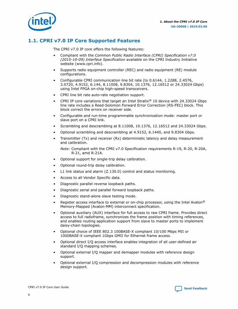
1. About the CPRI v7.0 IP CoreThe Common Public Radio Interface (CPRI) v7.0 Intel® FPGA IP core implements theCPRI Specification V7.0 (2015-10-09). CPRI is a high-speed serial interface fornetwork radio equipment controllers (REC) to receive data from and provide data toremote radio equipment (RE).
The CPRI v7.0 IP core targets high-performance, remote radio network applications.You can configure the CPRI v7.0 IP core as an RE or an REC.
Figure 1. Typical CPRI Application on Intel FPGA DevicesExample system implementation with a two-hop daisy chain. Optical links between devices support highperformance.
CPRI v7.0IP Core
(RE Slave)
FPGA FPGA
CPRI v7.0IP Core
(RE Slave)
CPRI v7.0IP Core
(RE Master)
FPGA
CPRI v7.0IP Core
(REC Master)
ClockModuleBase Band Module
Optical LinkOptical Link
CPRICPRICPRI
CPRI
Routing Layer
IQ Direct IQ DirectAUX AUX
UG-20008 | 2019.02.06
Send Feedback
Intel Corporation. All rights reserved. Intel, the Intel logo, Altera, Arria, Cyclone, Enpirion, MAX, Nios, Quartusand Stratix words and logos are trademarks of Intel Corporation or its subsidiaries in the U.S. and/or othercountries. Intel warrants performance of its FPGA and semiconductor products to current specifications inaccordance with Intel's standard warranty, but reserves the right to make changes to any products and servicesat any time without notice. Intel assumes no responsibility or liability arising out of the application or use of anyinformation, product, or service described herein except as expressly agreed to in writing by Intel. Intelcustomers are advised to obtain the latest version of device specifications before relying on any publishedinformation and before placing orders for products or services.*Other names and brands may be claimed as the property of others.
ISO9001:2015Registered
1.1. CPRI v7.0 IP Core Supported Features
The CPRI v7.0 IP core offers the following features:
• Compliant with the Common Public Radio Interface (CPRI) Specification v7.0(2015-10-09) Interface Specification available on the CPRI Industry Initiativewebsite (www.cpri.info).
• Supports radio equipment controller (REC) and radio equipment (RE) moduleconfigurations.
• Configurable CPRI communication line bit rate (to 0.6144, 1.2288, 2.4576,3.0720, 4.9152, 6.144, 8.11008, 9.8304, 10.1376, 12.16512 or 24.33024 Gbps)using Intel FPGA on-chip high-speed transceivers.
• CPRI line bit rate auto-rate negotiation support.
• CPRI IP core variations that target an Intel Stratix® 10 device with 24.33024 Gbpsline rate includes a Reed-Solomon Forward Error Correction (RS-FEC) block. Thisblock correct the errors on receiver side.
• Configurable and run-time programmable synchronization mode: master port orslave port on a CPRI link.
• Scrambling and descrambling at 8.11008, 10.1376, 12.16512 and 24.33024 Gbps.
• Optional scrambling and descrambling at 4.9152, 6.1440, and 9.8304 Gbps.
• Transmitter (Tx) and receiver (Rx) deterministic latency and delay measurementand calibration.
Note: Compliant with the CPRI v7.0 Specification requirements R-19, R-20, R-20A,R-21, amd R-21A.
• Optional support for single-trip delay calibration.
• Optional round-trip delay calibration.
• L1 link status and alarm (Z.130.0) control and status monitoring.
• Access to all Vendor Specific data.
• Diagnostic parallel reverse loopback paths.
• Diagnostic serial and parallel forward loopback paths.
• Diagnostic stand-alone slave testing mode.
• Register access interface to external or on-chip processor, using the Intel Avalon®
Memory-Mapped (Avalon-MM) interconnect specification.
• Optional auxiliary (AUX) interface for full access to raw CPRI frame. Provides directaccess to full radioframe, synchronizes the frame position with timing references,and enables routing application support from slave to master ports to implementdaisy-chain topologies.
• Optional choice of IEEE 802.3 100BASE-X compliant 10/100 Mbps MII or1000BASE-X compliant 1Gbps GMII for Ethernet frame access.
• Optional direct I/Q access interface enables integration of all user-defined airstandard I/Q mapping schemes.
• Optional external I/Q mapper and demapper modules with reference designsupport.
• Optional external I/Q compression and decompression modules with referencedesign support.
1. About the CPRI v7.0 IP Core
UG-20008 | 2019.02.06
CPRI v7.0 IP Core User Guide Send Feedback
6

• Optional vendor specific data access interfaces provide direct access to VendorSpecific (VS), Control AxC (Ctrl_AxC), and Real-time Vendor Specific (RTVS)subchannels.
• Optional HDLC serial interface provides direct access to slow control andmanagement subchannels.
• Optional L1 inband interface provides direct access to Z.130.0 link status andalarm control word.
Related Information
• CPRI Industry Initiative websiteFor a detailed specification of the CPRI protocol refer to the CPRI Specificationv7.0 (2015-10-09) Interface Specification available on the CPRI IndustryInitiative website.
• Intel FPGA Wiki CPRI IP Releases & SupportIncludes links to the releases, license information, I/Q mapper and other CPRIv7.0 IP core reference designs.
• Intel FPGA Design StoreIncludes CPRI reference designs.
1.2. CPRI v7.0 IP Core Device Family and Speed Grade Support
The following sections list the device family and device speed grade support offered bythe CPRI v7.0 IP core:
1.2.1. Device Family Support
Table 1. Intel FPGA IP Core Device Support Levels
Device SupportLevel
Definition
Advance The IP core is available for simulation and compilation for this device family. Timing models includeinitial engineering estimates of delays based on early post-layout information. The timing models aresubject to change as silicon testing improves the correlation between the actual silicon and the timingmodels. You can use this IP core for system architecture and resource utilization studies, simulation,pinout, system latency assessments, basic timing assessments (pipeline budgeting), and I/O transferstrategy (datapath width, burst depth, I/O standards tradeoffs).
Preliminary Intel has verified the IP core with preliminary timing models for this device family. The IP core meetsall functional requirements, but might still be undergoing timing analysis for the device family. It canbe used in production designs with caution.
Final Intel has verified the IP core with final timing models for this device family. The IP core meets allfunctional and timing requirements for the device family and can be used in production designs.
Table 2. CPRI v7.0 IP Core Device Family SupportShows the level of support offered by the CPRI v7.0 IP core for each Intel FPGA device family.
Device Family Support
Intel Stratix 10 Advance
Intel Arria® 10 Default support level provided in the Intel Quartus® Prime software. Refer to the Quartus PrimeStandard Edition Software and Device Support Release Notes and the Quartus Prime Pro EditionSoftware and Device Support Release Notes for the relevant software release.
continued...
1. About the CPRI v7.0 IP Core
UG-20008 | 2019.02.06
Send Feedback CPRI v7.0 IP Core User Guide
7

Device Family Support
Arria V (GX and GT) Default support level provided in Intel Quartus Prime Standard Edition software. Refer to theQuartus Prime Standard Edition Software and Device Support Release Notes for the relevantsoftware release.
Arria V GZ Default support level provided in Intel Quartus Prime Standard Edition software. Refer to theQuartus Prime Standard Edition Software and Device Support Release Notes for the relevantsoftware release.
Cyclone V (GX and GT) Default support level provided in Intel Quartus Prime Standard Edition software. Refer to theQuartus Prime Standard Edition Software and Device Support Release Notes for the relevantsoftware release.
Stratix V (GX and GT) Default support level provided in Intel Quartus Prime Standard Edition software. Refer to theQuartus Prime Standard Edition Software and Device Support Release Notes for the relevantsoftware release.
Other device families No support
Related Information
• CPRI v7.0 IP Core Performance: Device and Transceiver Speed Grade Support onpage 8
• Timing and Power ModelsReports the default device support levels in the current version of the IntelQuartus Prime Standard Edition software.
• Timing and Power ModelsReports the default device support levels in the current version of the IntelQuartus Prime Pro Edition software.
1.2.2. CPRI v7.0 IP Core Performance: Device and Transceiver SpeedGrade Support
Table 3. Slowest Supported Device Speed Grade and Supported Transceiver SpeedGradeLower device speed grade numbers correspond to faster devices. The entry -x indicates that both the industrialspeed grade Ix and the commercial speed grade Cx are supported for this device family and CPRI line bit rate.Table entries show slowest supported device speed grade / supported transceiver speed grade.
DeviceFamily
CPRI Line Bit Rate (Gbps)
0.6144 1.2288 2.4576 3.072 4.9152 6.1440 8.11008 9.8304 10.137
6 12.16512 24.33024
IntelStratix 10H-Tile andL-Tile
(1)
-2 / -3 -2 / -2
Intel Arria10
(1)-3 / -4 (1)
Stratix VGT -3 / H3 -2 / H2 (1)
Stratix VGX -4 / H3 -2 / H2 (1)
Arria V GZ -4 / H3 -3 / H2 (1)
continued...
(1) The CPRI v7.0 IP core does not support this CPRI line bit rate for this device family.
1. About the CPRI v7.0 IP Core
UG-20008 | 2019.02.06
CPRI v7.0 IP Core User Guide Send Feedback
8

DeviceFamily
CPRI Line Bit Rate (Gbps)
0.6144 1.2288 2.4576 3.072 4.9152 6.1440 8.11008 9.8304 10.137
6 12.16512 24.33024
Arria V GX -6 / H6 -5 /H4
-5 /H4
(1)
Arria V GT -5/H3 (1)
Cyclone VGT -7 / H5 (1)
Cyclone VGX
-8 /H7 -7 / H6 (1)
1.3. IP Core Verification
To ensure functional correctness of the CPRI v7.0 IP core, Intel performs extensivevalidation through both simulation and hardware testing. Before releasing a version ofthe CPRI v7.0 IP core, Intel runs basic regression tests in the associated version of theIntel Quartus Prime software.
Related Information
• Knowledge BaseSome exceptions to functional correctness are documented in the CPRI v7.0 IPcore errata.
• CPRI v7.0 Errata pageOther exceptions to functional correctness are documented on the Intel FPGAwiki CPRI v7.0 Errata page.
1.4. Resource Utilization for CPRI v7.0 IP Cores
Resource utilization changes depending on the parameter settings you specify in theCPRI v7.0 parameter editor. For example, with every additional interface you enable,the IP core requires additional resources to implement the module that supports thatinterface.
The resource utilization numbers are approximate as the Intel Quartus Prime Fitterassigns resources based on the entirety of your design. The numbers below resultfrom a single run on a simple design. Your results may vary.
Table 4. Minimum and Maximum IP Core Variations for Resource Utilization Reporting
The IP core FPGA resource utilization table reports resource utilization for a minimum IP core variation and amaximum IP core variation. Parameters not specified remain at their default values, or their values do notaffect resource utilization.
Parameter Minimum Variation Maximum Variation
Line bit rate 1.2288 Gbps for target device in theIntel Arria 10 and Intel Stratix 10device families, 0.6144 Gbps for allother device families
Maximum bit rate (device familydependent)
Synchronization mode Master Master
Operation mode TX/RX Duplex TX/RX Duplex
Core clock source input Internal Internal
continued...
1. About the CPRI v7.0 IP Core
UG-20008 | 2019.02.06
Send Feedback CPRI v7.0 IP Core User Guide
9

Parameter Minimum Variation Maximum Variation
Receiver soft buffer depth 4 8
Auxiliary and direct interfaceswrite latency cycle(s)
— 9
Enable interface, for all optional directinterfaces in the L1 Features tab
Off On
Ethernet PCS interface NONE GMII
L2 Ethernet PCS Tx/Rx FIFO depth — 11
Enable single-trip delay calibration Off Off
Enable round-trip delay calibration Off On
Round-trip delay calibration FIFOdepth
— 4
Table 5. IP Core FPGA Resource UtilizationLists the resources and expected performance for minimum and maximum variations of the CPRI v7.0 IP corein each supported device family.
These results were obtained using the Intel Quartus Prime Pro Edition v17.1 software on an Intel Stratix 10and Intel Arria 10 device, and using the Intel Quartus Prime Standard Edition v17.1 software for all othertarget device families.
• The numbers of ALMs and logic registers are rounded up to the nearest 100.
• The numbers of ALMs, before rounding, are the ALMs needed numbers from the Intel Quartus PrimeFitter Report.
Intel Stratix 10 Device (with H-Tile Transceivers) ALMs Logic Registers M20K Blocks
Minimum (1.2288 Gbps CPRI line bit rate) 1100 200 2
Maximum (24.33024 Gbps CPRI line bit rate) 17400 31200 44
Intel Arria 10 Device ALMs Logic Registers M20K Blocks
Minimum (1.2288 Gbps CPRI line bit rate) 800 1700 2
Maximum (10.1376 Gbps CPRI line bit rate) 3000 5000 16
Arria V GX or GT Device ALMs Logic Registers M10K Blocks
Minimum (0.6144 Gbps CPRI line bit rate) 900 1600 6
Maximum (6.144 Gbps CPRI line bit rate) 3200 5000 15
Arria V GZ Device ALMs Logic Registers M20K Blocks
Minimum (0.6144 Gbps CPRI line bit rate) 1000 1600 2
Maximum (9.8304 Gbps CPRI line bit rate) 3300 5100 9
Cyclone V GX or GT Device ALMs Logic Registers M10K Blocks
Minimum (0.6144 Gbps CPRI line bit rate) 900 1600 6
Maximum (4.9512 Gbps CPRI line bit rate) 3100 5000 11
1. About the CPRI v7.0 IP Core
UG-20008 | 2019.02.06
CPRI v7.0 IP Core User Guide Send Feedback
10

Stratix V GX or GT Device ALMs Logic Registers M20K Blocks
Minimum (0.6144 Gbps CPRI line bit rate) 900 1600 2
Maximum (10.1376 Gbps CPRI line bit rate) 3900 6000 18
Related Information
Fitter Resources Reports in the Intel Quartus Prime HelpInformation about Intel Quartus Prime resource utilization reporting, includingALMs needed.
1.5. Release Information
Table 6. CPRI v7.0 IP Core Current Release Information
Item Description
Compatible Intel Quartus Prime Software Version 17.1
Release Date 2018.09.19
Ordering Codes IP-CPRI-V7
1. About the CPRI v7.0 IP Core
UG-20008 | 2019.02.06
Send Feedback CPRI v7.0 IP Core User Guide
11

2. Getting Started with the CPRI v7.0 IP CoreExplains how to install, parameterize, and simulate the CPRI v7.0 IP core.
Installation and Licensing on page 12
Generating CPRI v7.0 IP Cores on page 13After you install and integrate the extended IP core in the ACDS release, the CPRIv7.0 IP core supports the standard customization and generation process. This IPcore is not supported in Platform Designer.
CPRI v7.0 IP Core File Structure on page 14
CPRI v7.0 IP Core Parameters on page 17
Integrating Your IP Core in Your Design: Required External Blocks on page 24
Simulating Intel FPGA IP Cores on page 32
Understanding the Testbench on page 32
Running the Testbench on page 33
Compiling the Full Design and Programming the FPGA on page 35
Related Information
Introduction to Intel FPGA IP IP CoresAdditional information about generating an Intel FPGA IP core and integrating it inyour Intel Quartus Prime project.
2.1. Installation and Licensing
The CPRI v7.0 IP core is an extended FPGA IP core which is not included with the IntelQuartus Prime release. This section provides a general overview of the Intel extendedFPGA IP core installation process to help you quickly get started with any Intelextended FPGA IP core.
The Intel extended FPGA IP cores are available from the Intel Self-Service LicensingCenter (SSLC). Refer to Related Information below for the correct link for this IP core.
UG-20008 | 2019.02.06
Send Feedback
Intel Corporation. All rights reserved. Intel, the Intel logo, Altera, Arria, Cyclone, Enpirion, MAX, Nios, Quartusand Stratix words and logos are trademarks of Intel Corporation or its subsidiaries in the U.S. and/or othercountries. Intel warrants performance of its FPGA and semiconductor products to current specifications inaccordance with Intel's standard warranty, but reserves the right to make changes to any products and servicesat any time without notice. Intel assumes no responsibility or liability arising out of the application or use of anyinformation, product, or service described herein except as expressly agreed to in writing by Intel. Intelcustomers are advised to obtain the latest version of device specifications before relying on any publishedinformation and before placing orders for products or services.*Other names and brands may be claimed as the property of others.
ISO9001:2015Registered

Figure 2. IP Core Installation Directory StructureDirectory structure after you install the CPRI v7.0 IP core.
Intel Quartus Prime installation directory
ipContains the Intel FPGA IP Library and third-party IP cores
altera_cloudContains the Intel FPGA extended IP cores that you install
cpri_iiContains the CPRI v7.0 IP core files
Table 7. IP Core Installation Locations
Location Software Platform
<drive>:\intelFPGA_pro\<version>\quartus\ip\altera_cloud
Intel Quartus Prime Pro Edition Windows*
<drive>:\intelFPGA\<version>\quartus\ip\altera_cloud
Intel Quartus Prime StandardEdition
Windows
<home directory>:/intelFPGA_pro/<version>/quartus/ip/altera_cloud
Intel Quartus Prime Pro Edition Linux*
<home directory>:/intelFPGA/<version>/quartus/ip/altera_cloud
Intel Quartus Prime StandardEdition
Linux
Related Information
• Intel FPGA website
• Self-Service Licensing Center (SSLC)After you purchase the CPRI v7.0 IP core, the IP core is available for downloadfrom the SSLC page in your My Intel account. You must create a My Intelaccount if you do not have one already, and log in to access the SSLC. On theSSLC page, click Run for this IP core. The SSLC provides an installation dialogbox to guide your installation of the IP core.
2.2. Generating CPRI v7.0 IP Cores
You can quickly configure a custom IP variation in the parameter editor. Use thefollowing steps to specify CPRI v7.0 IP core options and parameters in the parametereditor.
1. In the Intel Quartus Prime Pro Edition software, click File ➤ New Project Wizardto create a new Intel Quartus Prime project, or File ➤ Open Project to open anexisting Intel Quartus Prime project. The wizard prompts you to specify a device.In the Intel Quartus Prime Standard Edition software, this step is not required.
2. In the IP Catalog (Tools ➤ IP Catalog), locate and double-click the name CPRI.The parameter editor appears.
3. Specify a top-level name for your custom IP variation. The parameter editor savesthe IP variation settings in a file named <your_ip>.ip (in Intel Quartus Prime ProEdition). Click OK.
2. Getting Started with the CPRI v7.0 IP Core
UG-20008 | 2019.02.06
Send Feedback CPRI v7.0 IP Core User Guide
13

4. Specify the parameters and options for your IP variation in the parameter editor,including one or more of the following. Refer to IP Core Parameters for informationabout specific IP core parameters.
• Specify parameters defining the IP core functionality, port configurations, anddevice-specific features.
• Specify options for processing the IP core files in other EDA tools.
5. Click Generate HDL. The Generation dialog box appears.
6. Specify output file generation options, and then click Generate. The IP variationfiles generate according to your specifications.
7. To generate a simulation testbench, click Generate Example Design. Pleaserefer to the instructions in the Running the Testbench section.
8. To generate an HDL instantiation template that you can copy and paste into yourtext editor, click Generate ➤ Show Instantiation Template.
9. Click Finish. The parameter editor adds the top-level .qsys or .ip file to thecurrent project automatically. If you are prompted to manually add the .qsys fileto the project, click Project ➤ Add/Remove Files in Project to add the file.
10. After generating and instantiating your IP variation, make appropriate pinassignments to connect ports.
2.3. CPRI v7.0 IP Core File Structure
The Intel Quartus Prime software generates the following IP core output file structure.
2. Getting Started with the CPRI v7.0 IP Core
UG-20008 | 2019.02.06
CPRI v7.0 IP Core User Guide Send Feedback
14

Figure 3. IP Core Generated Files
<your_ip>.cmp - VHDL component declaration file
<your_ip>.ppf - XML I/O pin information file
<your_ip>.qip - Lists IP synthesis files
<your_ip>.sip - Lists files for simulation
<your_ip>.v or .vhdTop-level IP synthesis file
<your_ip>.v or .vhdTop-level simulation file
<simulator_setup_scripts>
<your_ip>.ip - System or IP integration file
<your_ip>_bb.v - Verilog HDL black box EDA synthesis file
<your_ip>_inst.v or .vhd - Sample instantiation template
<your_ip>_generation.rpt - IP generation report
<your_ip>.debuginfo - Contains post-generation information (Standard Edition only)
<your_ip>.html - Connection and memory map data
<your_ip>.bsf - Block symbol schematic
<your_ip>.spd - Combines individual simulation scripts
<your_ip>.sopcinfo - Software tool-chain integration file (Standard Edition only)
<project directory>
<your_ip>
IP variation files
cpri_ii_0_testbench
Example location for your IP core design example files. The default location is cpri_ii_0_testbench, butyou are prompted to specify a different path (Pro Edition only)
sim
Simulation files
synth
IP synthesis files
<EDA tool name>
Simulator scripts
<ip subcores_ver>Subcore libraries
simSubcore
Simulation files
synthSubcore
synthesis files
<HDL files><HDL files>
<your_ip>_<n>
IP variation files
<your_ip>.qgsynthc - Lists synthesis parameters to support incremental regeneration (Pro Edition only)
<your_ip>.qgsimc - Lists simulation parameters to support incremental regeneration (Pro Edition only)
(1)
Note:(1) For V-series device variations, the testbench directory is <your_ip>_testbench/altera_cpri_ii
Table 8. IP Core Generated Files
File Name Description
<your_ip>.ip (Intel Quartus Prime ProEdition only)
Top-level IP variation file. <your_ip> is the name that you give your IPvariation.
Note: The Intel Quartus Prime Standard Edition software creates differentsource files for your CPRI IP variation.
<system>.sopcinfo Describes the connections and IP component parameterizations in yourPlatform Designer system. You can parse its contents to get requirementswhen you develop software drivers for IP components. (Intel Quartus PrimeStandard Edition only)
continued...
2. Getting Started with the CPRI v7.0 IP Core
UG-20008 | 2019.02.06
Send Feedback CPRI v7.0 IP Core User Guide
15
File Name Description
Downstream tools such as the Intel Nios® II tool chain use this file.The .sopcinfo file and the system.h file generated for the Nios II tool chaininclude address map information for each slave relative to each master thataccesses the slave. Different masters may have a different address map toaccess a particular slave component.
<your_ip>.cmp The VHDL Component Declaration (.cmp) file is a text file that contains localgeneric and port definitions that you can use in VHDL design files.
<your_ip>.html A report that contains connection information, a memory map showing theaddress of each slave with respect to each master to which it is connected, andparameter assignments.
<your_ip>_generation.rpt IP or Platform Designer generation log file. A summary of the messages duringIP generation.
<your_ip>.debuginfo Contains post-generation information. Used to pass System Console and BusAnalyzer Toolkit information about the Platform Designer (Standard)interconnect. The Bus Analysis Toolkit uses this file to identify debugcomponents in the Platform Designer (Standard) interconnect. (Intel QuartusPrime Standard Edition only)
<your_ip>.qgsimc Lists simulation parameters to support incremental regeneration. (IntelQuartus Prime Pro Edition only)
<your_ip>.qgsynthc Lists synthesis parameters to support incremental regeneration. (Intel QuartusPrime Pro Edition only)
<your_ip>.qip Contains all the required information about the IP component to integrate andcompile the IP component in the Quartus Prime software.
<your_ip>.csv Contains information about the upgrade status of the IP component.
<your_ip>.bsf A Block Symbol File (.bsf) representation of the IP variation for use in QuartusPrime Block Diagram Files (.bdf).
<your_ip>.spd Required input file for ip-make-simscript to generate simulation scripts forsupported simulators. The .spd file contains a list of files generated forsimulation, along with information about memories that you can initialize.
<your_ip>.ppf The Pin Planner File (.ppf) stores the port and node assignments for IPcomponents created for use with the Pin Planner.
<your_ip>_bb.v You can use the Verilog black-box (_bb.v) file as an empty module declarationfor use as a black box.
<your_ip>.sip Contains information required for NativeLink simulation of IP components. Youmust add the .sip file to your Intel Quartus Prime project.
<your_ip>_inst.v and _inst.vhd HDL example instantiation template. You can copy and paste the contents ofthis file into your HDL file to instantiate the IP variation.
<your_ip>.regmap If IP contains register information, .regmap file generates. The .regmap filedescribes the register map information of master and slave interfaces. This filecomplements the .sopcinfo file by providing more detailed register informationabout the system. This enables register display views and user customizablestatistics in the System Console.
<your_ip>.svd Allows hard processor system (HPS) System Debug tools to view the registermaps of peripherals connected to HPS within a Platform Designer system.During synthesis, the .svd files for slave interfaces visible to System Consolemasters are stored in the .sof file in the debug section. System Console readsthis section, which Platform Designer can query for register map information.For system slaves, Platform Designer can access the registers by name.
<your_ip>.v
and<your_ip>.vhd
HDL files that instantiate each submodule or child IP core for synthesis orsimulation.
continued...
2. Getting Started with the CPRI v7.0 IP Core
UG-20008 | 2019.02.06
CPRI v7.0 IP Core User Guide Send Feedback
16

File Name Description
mentor/ Contains a ModelSim script msim_setup.tcl to set up and run a simulation.
aldec/ Contains a Riviera-PRO script rivierapro_setup.tcl to setup and run asimulation.
synopsys/vcs/
synopsys/vcsmx/
Contains a shell script vcs_setup.sh to set up and run a VCS® simulation.Contains a shell script vcsmx_setup.sh and synopsys_ sim.setup file toset up and run a VCS MX® simulation.
cadence/ Contains a shell script ncsim_setup.sh and other setup files to set up andrun an NCSIM simulation.
submodules/ Contains HDL files for the IP core submodule.
<child IP cores>/ For each generated child IP core directory, Platform Designer generatessynth/ andsim/ sub-directories.
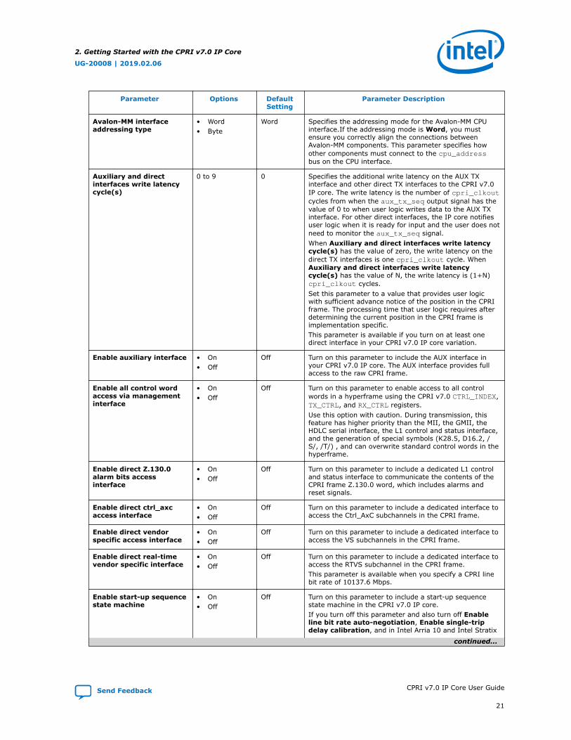
2.4. CPRI v7.0 IP Core Parameters
The CPRI v7.0 parameter editor provides the parameters you can set to configure theCPRI v7.0 IP core and simulation testbench.
The CPRI v7.0 parameter editor has three tabs.
Table 9. General CPRI v7.0 IP Core ParametersDescribes the general parameters for customizing the CPRI v7.0 IP core. These parameters appear on theGeneral tab in the CPRI v7.0 parameter editor.
Parameter Options DefaultSetting
Parameter Description
Selected device family • Intel Stratix 10• Intel Arria 10• Stratix V• Arria V• Cyclone® V
Specifies the target device.
Line bit rate (Mbits/s) • 614.4• 1228.8• 2457.6• 3072.0• 4915.2• 6144.0• 8110.08• 9830.4• 10137.6• 12165.12• 24330.24
Lowestbit ratesupported for thedevicefamily
Selects the CPRI line bit rate. Refer to CPRI v7.0 IP CorePerformance: Device and Transceiver Speed Grade Supporton page 8 for supported CPRI line bit rates in the supporteddevice families.The parameter editor does not allow you to specify a CPRIline bit rate that the target device does not support.
Data path width • 32• 64
32 This parameter specifies interface width.CPRI IP core variations that target Intel Stratix 10 devicewith line bit rate value 12165.12 or 24330.24 Mbps, thisparameter value is 64.For all other device variations and combinations, thisparameter value is 32.
Synchronization mode • Master• Slave
Master Specifies whether the CPRI v7.0 IP core is configured as aCPRI link master or a CPRI link slave.
continued...
2. Getting Started with the CPRI v7.0 IP Core
UG-20008 | 2019.02.06
Send Feedback CPRI v7.0 IP Core User Guide
17

Parameter Options DefaultSetting
Parameter Description
The value of this parameter determines the initial and resetclocking mode of the CPRI v7.0 IP core. You can modify theIP core clocking mode dynamically by modifying the value ofthe synchronization_mode field of the L1_CONFIGregister.
Operation mode • TX/RX Duplex• TX Simplex• RX Simplex
TX/RXDuplex
Specifies whether the CPRI v7.0 IP core is configured withRX functionality only (RX Simplex), with TX functionalityonly (TX Simplex), or with both RX and TX functionality(TX/TX Duplex).If you specify a simplex mode, the Quartus Prime Fittersynthesizes logic for only one direction of traffic. If the CPRIv7.0 IP core is in TX simplex operation mode, it can transmiton the CPRI link but cannot receive. If the CPRI v7.0 IP coreis in RX simplex operation mode, it can receive traffic on theCPRI link but cannot transmit.
Core clock source input • External• Internal• Hybrid
Internal Specifies the clock source of the cpri_clkout port thatdrives the core.The external clocking scheme supports the single-trip delaycalibration feature. In this clocking scheme, the clock fedthrough cpri_coreclk drives the cpri_clkout at allCPRI line bit rates.In the internal clocking scheme, the clock from thetransceiver PHY drives the cpri_clkout.The hybrid option is available only when you select at leastone CPRI line bit rate from Group 1 and Group 2 of the tablebelow and enable line bit rate auto-negotiation parameter:
Group 1 (Gbps) Group 2 (Gbps)
0.6144, 1.2288, 2.4576,3.072, 4.9152, 6.1440
8.11008, 9.8304, 10.1376,12.16512, 24.33024
In hybrid mode, the IP works in the Internal clockingscheme when you select CPRI line bit rates from Group 1and works in external mode clocking scheme when youselect the CPRI line bit rates from Group 2.
Transmitter local clockdivision factor
• 1• 2• 4• 8
1 Specifies the division factor for the local clock divider. The IPcore divides the high speed clock from the transceiver TXPLL (xcvr_ext_pll_clk) to generate the serial TX clock.This feature supports the configuration of multiple instancesof the CPRI v7.0 IP core that run at different CPRI line bitrates but share use of the same TX PLL.This parameter is not available if you set the value ofOperation mode to RX Simplex.IP core variations that target an Intel Arria 10 device or anIntel Stratix 10 device, with Line bit rate set to 4915.2Mbps or slower, support only the value of 1.
Number of receiver CDRreference clock(s)
• 1• 2
1 Specifies the width of the receiver reference clock thatcontrols the receiver. The CPRI v7.0 IP core supports theselection of one or two clocks. This option supports auto-negotiation to and from the CPRI line bit rate of 10.1376Gbps in CPRI v7.0 IP core variations that target a Stratix Vdevice. Refer to "IP Core Clocking Structure."If you set this parameter to the value of 1, thexcvr_cdr_refclk is a single clock. If you set thisparameter to the value of 2, the xcvr_cdr_refclk inputsignal is two bits wide, to support two distinct referenceclocks.
continued...
2. Getting Started with the CPRI v7.0 IP Core
UG-20008 | 2019.02.06
CPRI v7.0 IP Core User Guide Send Feedback
18

Parameter Options DefaultSetting
Parameter Description
Intel recommends that you specify a two-bit clock forStratix V variations that are expected to implement auto-negotiation up to a 10.1376 Gbps CPRI line bit rate. In thiscase the typical design drives one bit of thexcvr_cdr_refclk clock with a common 307.2 MHz clockfor the lower CPRI line bit rates and drives the other bit witha 253.44 MHz clock for the 10.1376 Gbps CPRI line bit rate.However, these specific clock frequencies are not required.If the value of this parameter is 2, the receiver clocks theCDR with the xcvr_cdr_refclk[0] input signal bydefault. You can switch the receiver to usexcvr_cdr_refclk[1], or back to xcvr_cdr_refclk[0],by dynamically reconfiguring the RX transceiver.IP core variations that target a device family other than theStratix V device family, support only a single-bit receiverreference clock.CPRI IP core variations that target an Intel Arria 10 or anIntel Stratix 10 device family, support single and two bitreceiver CDR reference clock in the following conditions:• Intel Arria 10 devices with auto-rate negotiation on and
with the CPRI line bit rate is 8.11008 Gbps or greater.• Intel Stratix 10 devices with auto-rate negotiation option
on.For all other cases, set this parameter value to 1.This parameter is not available if you set the value ofOperation mode to TX Simplex.
Receiver CDR referenceclock frequency (MHz)
Per drop-downmenu
307.2 Specifies the incoming reference clock frequency for thereceiver CDR PLL, in MHz.You must drive the input clock xcvr_cdr_refclk orxcvr_cdr_refclk[0] at the frequency you specify for thisparameter.This parameter is not available if you set the value ofOperation mode to TX Simplex.
VCCR_GXB andVCCT_GXB supplyvoltage for thetransceiver
• 1_1V• 1_0V
1_1V Specifies whether the transceiver supply voltage is 1.1 V or1.0 V. The supply voltage must match the voltage youspecify for this parameter, in IP core variations that targetan Intel Stratix 10 device.This parameter affects only IP core variations that target anIntel Stratix 10 device. You can ignore it for other devicefamilies.
Recovered clock source • PCS• PMA
PCS Specifies the clock source of the xcvr_recovered_clk.Intel recommends that you set this parameter to the valueof PMA in IP core variations that target a Stratix V device, ifyou expect your IP core to auto-negotiate to or from theCPRI line bit rate of 10.1376 Gbps. In this case, sourcingthe recovered clock from the PMA improves jitter on thatclock. If you specify the PCS source, the IP core switchesbetween two PCS-internal clocks at auto-negotiation to orfrom the CPRI line bit rate of 10.1376 Gbps.This parameter is not available for• CPRI master IP cores• IP cores that target an Intel Stratix 10 device• IP cores for which you set the value of Operation mode
to TX Simplex
Receiver soft bufferdepth
4, 5, 6, 7, or 8 6 The value you specify for this parameter is log2 of the IPcore Layer 1 Rx buffer depth.The IP core supports amaximum Layer 1 RX buffer depth of 256.
continued...
2. Getting Started with the CPRI v7.0 IP Core
UG-20008 | 2019.02.06
Send Feedback CPRI v7.0 IP Core User Guide
19

Parameter Options DefaultSetting
Parameter Description
The default depth of the buffer is 64, specified by theparameter default value of 6. For most systems, the defaultbuffer depth is adequate to handle dispersion, jitter, anddrift that can occur on the link while the system is running.However, the parameter is available for cases in whichadditional depth is required.Increasing the value of this parameter increases resourceutilization. Increasing the value of this parameter affectslatency only when the buffer fills beyond the defaultcapacity. In that case, the larger buffer increases latencybut prevents data loss.The user guide refers to this parameter value asRX_BUF_DEPTH.This parameter is not available if you set the value ofOperation mode to TX Simplex.
Enable line bit rateauto-negotiation
• On• Off
Off Turn on the Enable line bit rate auto-negotiationparameter to specify that your CPRI v7.0 IP core supportsauto-rate negotiation.If you turn on this parameter, your IP core does notimplement auto-negotiation. You must dynamicallyreconfigure the transceiver to modify the CPRI line bit rateand implement auto-negotiation. However, if you turn offthis parameter, the IP core does not support bit line rateauto-negotiation, and you cannot modify the CPRI line bitrate dynamically.If you turn off this parameter and also turn off Enablestart-up sequence state machine, Enable single-tripdelay calibration, and in Intel Arria 10 and Intel Stratix 10devices, the Enable ADME, transceiver capability,control and status registers access, the transceiverreconfiguration interface is not available.This parameter is only available for Intel Arria 10 and IntelStratix 10 devices when you specify a CPRI line bit rate(value for the Line bit rate parameter) that is greater than1228.8 Mbps.
• 614.4 Mbit/s• 1228.8 Mbit/s• 2457.6 Mbit/s• 3072.0 Mbit/s• 4915.2 Mbit/s• 6144.0 Mbit/s• 8110.08 Mbit/s• 9830.4 Mbit/s• 10137.6 Mbit/s• 12165.12 Mbit/s
• On• Off
Off These options are available when you turn on Enable linebit rate auto-negotiation parameter. You must select aCPRI line bit rate (value of the Line bit rate (Mbit/s)parameter) that is greater than one or more line bit rate (s)which you would like to negotiate to.You must choose at least one value to rate negotiate to ifyou turn on line bit rate auto-negotiation.
Table 10. CPRI v7.0 IP Core Interface Feature ParametersDescribes the parameters for customizing the CPRI v7.0 IP core Layer 1 and Layer 2 interfaces and testingfeatures. These parameters appear on the Interfaces tab in the CPRI v7.0 parameter editor.
Parameter Options DefaultSetting
Parameter Description
L1 Features
Management (CSR)interface standard
Currently, only the Avalon-MMCPU interface is available inthe CPRI v7.0 IP core.
Selects the interface specification that describes thebehavior of the CPRI v7.0 IP core register accessinterface.
continued...
2. Getting Started with the CPRI v7.0 IP Core
UG-20008 | 2019.02.06
CPRI v7.0 IP Core User Guide Send Feedback
20
Parameter Options DefaultSetting
Parameter Description
Avalon-MM interfaceaddressing type
• Word• Byte
Word Specifies the addressing mode for the Avalon-MM CPUinterface.If the addressing mode is Word, you mustensure you correctly align the connections betweenAvalon-MM components. This parameter specifies howother components must connect to the cpu_addressbus on the CPU interface.
Auxiliary and directinterfaces write latencycycle(s)
0 to 9 0 Specifies the additional write latency on the AUX TXinterface and other direct TX interfaces to the CPRI v7.0IP core. The write latency is the number of cpri_clkoutcycles from when the aux_tx_seq output signal has thevalue of 0 to when user logic writes data to the AUX TXinterface. For other direct interfaces, the IP core notifiesuser logic when it is ready for input and the user does notneed to monitor the aux_tx_seq signal.When Auxiliary and direct interfaces write latencycycle(s) has the value of zero, the write latency on thedirect TX interfaces is one cpri_clkout cycle. WhenAuxiliary and direct interfaces write latencycycle(s) has the value of N, the write latency is (1+N)cpri_clkout cycles.Set this parameter to a value that provides user logicwith sufficient advance notice of the position in the CPRIframe. The processing time that user logic requires afterdetermining the current position in the CPRI frame isimplementation specific.This parameter is available if you turn on at least onedirect interface in your CPRI v7.0 IP core variation.
Enable auxiliary interface • On• Off
Off Turn on this parameter to include the AUX interface inyour CPRI v7.0 IP core. The AUX interface provides fullaccess to the raw CPRI frame.
Enable all control wordaccess via managementinterface
• On• Off
Off Turn on this parameter to enable access to all controlwords in a hyperframe using the CPRI v7.0 CTRL_INDEX,TX_CTRL, and RX_CTRL registers.Use this option with caution. During transmission, thisfeature has higher priority than the MII, the GMII, theHDLC serial interface, the L1 control and status interface,and the generation of special symbols (K28.5, D16.2, /S/, /T/) , and can overwrite standard control words in thehyperframe.
Enable direct Z.130.0alarm bits accessinterface
• On• Off
Off Turn on this parameter to include a dedicated L1 controland status interface to communicate the contents of theCPRI frame Z.130.0 word, which includes alarms andreset signals.
Enable direct ctrl_axcaccess interface
• On• Off
Off Turn on this parameter to include a dedicated interface toaccess the Ctrl_AxC subchannels in the CPRI frame.
Enable direct vendorspecific access interface
• On• Off
Off Turn on this parameter to include a dedicated interface toaccess the VS subchannels in the CPRI frame.
Enable direct real-timevendor specific interface
• On• Off
Off Turn on this parameter to include a dedicated interface toaccess the RTVS subchannel in the CPRI frame.This parameter is available when you specify a CPRI linebit rate of 10137.6 Mbps.
Enable start-up sequencestate machine
• On• Off
Off Turn on this parameter to include a start-up sequencestate machine in the CPRI v7.0 IP core.If you turn off this parameter and also turn off Enableline bit rate auto-negotiation, Enable single-tripdelay calibration, and in Intel Arria 10 and Intel Stratix
continued...
2. Getting Started with the CPRI v7.0 IP Core
UG-20008 | 2019.02.06
Send Feedback CPRI v7.0 IP Core User Guide
21

Parameter Options DefaultSetting
Parameter Description
10 devices, the Enable ADME, transceiver capability,control and status registers access, the transceiverreconfiguration interface is not available.This parameter is available if you set the value ofOperation mode to TX/RX Duplex.
Enable protocol versionand C&M channel settingauto-negotiation
• On• Off
Off Turn on this parameter to include a negotiator block thatperforms auto-negotiation of L1 inband protocol version(communicated in CPRI frame position Z.2.0) and L2 C&Mrates (communicated in CPRI frame positions Z.66.0 andZ.194.0).This parameter is available when you turn on Enablestart-up sequence state machine.
Enable direct I/Qmapping interface
• On• Off
Off Turn on this parameter to include a dedicated interface toaccess the raw I/Q data bytes in the CPRI frame.
L2 Features
Enable HDLC serialinterface
• On• Off
Off Turn on this parameter to include a dedicated interface tocommunicate the contents of the slow C&M subchannels.For full HDLC communication, you must connect a user-defined HDLC module to this interface.
Ethernet PCS interface • NONE• MII• GMII
NONE Specify whether to include an MII or GMII port tocommunicate with the fast C&M (Ethernet) CPRIsubchannel. You can also specify that the IP core does notsupport either interface.• An MII port complies with the IEEE 802.3 100BASE-X
100Mbps MII specification,• A GMII port complies with the IEEE 802.3 1000BASE-
X 1Gbps GMII specification.For full Ethernet communication, you must connect auser-defined Ethernet MAC to this interface.GMII option is not available for CPRI IP core variationsthat target Intel Stratix 10 device with line bit rate value12165.12 or 24330.24 Mbps.
L2 Ethernet PCS Tx/Rxbuffer depth
7, 8, 9, 10, 11 7 The value you specify for this parameter is log2 of the IPcore Layer 2 Ethernet PCS Rx buffer depth and Tx bufferdepth. The IP core supports a maximum Layer 2 EthernetPCS buffer depth of 1024 for MII and 2048 for GMII.This parameter is available when you include an MII orGMII port to communicate with the fast C&M (Ethernet)CPRI subchannel by selecting the value of MII or GMIIfor the Ethernet PCS interface parameter.The new value of 11 is supported only for GMII.
Debug Features
Enable L1 debuginterfaces
• On• Off
Off Turn on this parameter to include dedicated transceiverstatus and L1 Rx status interfaces to support debug.This parameter is not available if you set the value ofOperation mode to TX Simplex.
Enable ADME, transceivercapability, control andstatus registers access
• On• Off
Off Turn on this parameter to support debugging through theSystem Console and to expose transceiver registers. Ifyou turn off this parameter and also turn off Enable linebit rate auto-negotiation, Enable start-up sequencestate machine, and Enable single-trip delaycalibration, the Intel Arria 10 or Intel Stratix 10transceiver reconfiguration interface is not available.This parameter is available only for Intel Arria 10 andIntel Stratix 10 devices.
continued...
2. Getting Started with the CPRI v7.0 IP Core
UG-20008 | 2019.02.06
CPRI v7.0 IP Core User Guide Send Feedback
22

Parameter Options DefaultSetting
Parameter Description
Enable transceiver PMAserial forward loopbackpath
• On• Off
Off Turn on this parameter to enable transceiver PMA serialforward loopback. To turn on transceiver PMA serialforward loopback (Tx to Rx), you must also write thevalue of 2'b01 to the loop_forward field of theLOOPBACK register at offset 0x44.This parameter is not available if you set the value ofOperation mode to TX Simplex or to RX Simplex.
Enable parallel forwardloopback paths
• On• Off
Off Turn on this parameter to enable other internal parallelforward loopback paths (Tx to Rx). To turn on internalparallel forward loopback, you must also write a non-zerovalue to the loop_forward field of the LOOPBACKregister at offset 0x44.This parameter is not available if you set the value ofOperation mode to TX Simplex or to RX Simplex.
Enable parallel reversedloopback paths
• On• Off
Off Turn on this parameter to enable internal parallel reverseloopback (Rx to Tx). To turn on reverse loopback, youmust also write a non-zero value to the loop_reversedfield of the LOOPBACK register at offset 0x44, to specifythe parts of the CPRI frame that are sent on the loopbackpath.This parameter is not available if you set the value ofOperation mode to TX Simplex or to RX Simplex.
Table 11. CPRI v7.0 IP Core Advanced Feature ParametersDescribes the parameters for customizing the CPRI v7.0 IP core delay calibration features. These parametersappear on the Advanced tab in the CPRI v7.0 parameter editor.
Parameter Options DefaultSetting
Parameter Description
Enable single-trip delaycalibration
• On• Off
Off Turn on this parameter to specify that your CPRI v7.0 IPcore supports single-trip delay calibration.If you turn on this parameter, your IP core implementssingle-trip delay calibration only if you connect itaccording to Adding and Connecting the Single-Trip DelayCalibration Blocks on page 30. Intel provides therequired external blocks but you must connect them tothe IP core in your design.This parameter is only available in IP core variations thattarget an Intel Arria 10 device.If you turn off this parameter and also turn off Enableline bit rate auto-negotiation, Enable start-upsequence state machine the transceiverreconfiguration interface is not available.This parameter is available only if you set the value of theCore clock source input parameter to External.
Enable round-trip delaycalibration
• On• Off
Off Turn on this parameter to to specify that your CPRI v7.0IP core supports round-trip delay calibration.This parameter is available only if you set the value of theSynchronization mode parameter to Master.
Round-trip delaycalibration FIFO depth
• 2• 3• 4
2 The value you specify for this parameter is log2 of the IPcore RTD calibration buffer depth.The IP core supports amaximum RTD calibration buffer depth of 16.The default depth of the buffer is 4, specified by theparameter default value of 2. For buffer depth N, theRead pointer can move (N/2)-1 entries in either directionfrom its initial state.
2. Getting Started with the CPRI v7.0 IP Core
UG-20008 | 2019.02.06
Send Feedback CPRI v7.0 IP Core User Guide
23

Table 12. CPRI v7.0 IP Core Simulation ParametersDescribes the parameters for customizing the CPRI v7.0 IP core delay calibration features. These parametersappear on the Advanced tab in the CPRI v7.0 parameter editor.
Parameter Options DefaultSetting
Parameter Description
Language for top-levelsimulation file
• Verilog• VHDL
Verilog This parameter determines the language of the top-levelsimulation file.
Related Information
• LOOPBACK Register on page 124
• CPRI v7.0 IP Core Clocking Structure on page 38
2.5. Integrating Your IP Core in Your Design: Required ExternalBlocks
You must connect your CPRI v7.0 IP core to some additional required designcomponents. Your design can simulate and compile without some of these connectionsand logical blocks, but it will not function correctly in hardware unless all of them arepresent and connected in your design.
The CPRI v7.0 IP core requires that you define, instantiate, and connect the followingadditional software and hardware modules for all CPRI v7.0 IP core variations:
• An external PLL IP core to configure the transceiver TX PLL. Although the FPGAelements this IP core configures are physically part of the device transceiver, youmust instantiate this IP core in software separately from the CPRI v7.0 IP core. InIntel Arria 10 and Intel Stratix 10 devices, this requirement supports theconfiguration of multiple Intel FPGA IP cores using the same transceiver block inthe device.
• One or more external reset controllers to coordinate the reset sequence for theCPRI v7.0 IP core in your design.
In addition, some IP core variations require additional modules to function correctly inhardware.
• CPRI link slave modules require an off-chip clean-up PLL.
• Variations that target a 28-nm device (Arria V, Arria V GZ, Cyclone V, or Stratix Vdevice family) require an external transceiver reconfiguration controller.
• Variations with the single-trip delay calibration feature require additional blocksthat Intel provides but does not connect in your design.
2. Getting Started with the CPRI v7.0 IP Core
UG-20008 | 2019.02.06
CPRI v7.0 IP Core User Guide Send Feedback
24

Figure 4. Required External BlocksAn example showing how you could connect required components to a single CPRI v7.0 IP core that targets anArria 10 device.
Reset Controller
Reset Controller
TXPLL
Transmitter(Native PHY)
Receiver(Native PHY)
User-DefinedReference Clock
xcvr_ext_pll_clk
xcvr_tx_analogresetxcvr_tx_digitalresetxcvr_tx_cal_busy
xcvr_rx_analogresetxcvr_rx_digitalresetxcvr_rx_is_lockedtodataxcvr_rx_cal_busy
xcvr_cdr_refclk
reset_tx_n
reset_rx_n
pll_locked
CPRI v7.0 IP Core
xcvr_reset_tx_ready
xcvr_reset_rx_ready
Related Information
Adding the Reset Controller on page 27
2.5.1. Adding the Transceiver TX PLL IP Core
The CPRI v7.0 IP core requires that you generate and connect a TX transceiver PLL IPcore. The transceiver PLL IP core configures the TX PLL in the transceiver on thedevice, but you must generate the transceiver PLL IP core separately from the CPRIv7.0 IP core in software. If you do not generate and connect the transceiver PLL IPcore, the CPRI v7.0 IP core does not compile.
You can use the IP Catalog to generate the external PLL IP core that configures a TXPLL on the device. In the IP Catalog, select an Intel FPGA IP core that configures anappropriate PLL on your target device.
For your 28-nm design, you can select Altera PLL (FPLL) or Transceiver PLL v17.1in the IP Catalog. In the parameter editor for the TX PLL IP core you select, you mustset the PLL output frequency to the expected input frequency for the CPRI v7.0 IPcore xcvr_ext_pll_clk input signal.
2. Getting Started with the CPRI v7.0 IP Core
UG-20008 | 2019.02.06
Send Feedback CPRI v7.0 IP Core User Guide
25

For your Intel Arria 10 design, you can select Arria 10 Transceiver ATX PLL, Arria10 Transceiver CMU PLL, or Arria 10 FPLL in the IP Catalog. For your Intel Stratix10 design, you can select one of the Transceiver PLL options available for your devicetile type in the IP Catalog. In the parameter editor for the TX PLL IP core you select,you must set the following parameter values:
• PLL output frequency to one half the per-lane data rate of the IP core variation,multiplied by the value of the Transmitter local clock division factor parameterof the CPRI v7.0 IP core. The transceiver performs dual edge clocking, using boththe rising and falling edges of the input clock from the PLL. Therefore, this PLLoutput frequency setting drives the transceiver with the correct clock for the CPRIv7.0 IP core line bit rate.
For example, if your CPRI v7.0 IP core variation has a CPRI line bit rate of 10.1376Gbps and you set the Transmitter local clock division factor parameter to thevalue of 1, you must set the TX PLL PLL output frequency parameter to thevalue of 5068.8 MHz.
• PLL reference clock frequency to a frequency at which you can drive the TXPLL input reference clock. You must drive the external PLL reference clock inputsignal at the frequency you specify for this parameter.
For example, if your CPRI v7.0 IP core variation has a CPRI line bit rate of 10.1376Gbps and you set the Transmitter local clock division factor parameter to thevalue of 1, you can set the PLL reference clock frequency to the value of 307.2MHz.
Intel Arria 10 and Intel Stratix 10 devices and the Intel Quartus Prime softwaresupport multiple options for configuring an Intel Arria 10 TX PLL or Intel Stratix 10 TXPLL. Depending on the TX PLL IP core you select and the configuration options youprefer, you have a wide range of choices in parameterizing the external TX PLL for adesign that targets one of these two device families.
You must connect the external TX PLL signals and the CPRI v7.0 IP core transceiver TXPLL interface signals according to the following rules.
Table 13. Required Connections Between Transceiver TX PLL and CPRI v7.0 IP CoreConnect the xcvr_ext_pll_clk input signal of the CPRI v7.0 IP core to the pll_clkout, tx_serial_clk,or outclk0 output signal of the external PLL IP core. Information about connecting the transceiver TX PLL tothe Reset Controller is available in Adding the Reset Controller on page 27.
CPRI v7.0 IP Core Signal TX PLL Signal
xcvr_ext_pll_clk (input) Intel Arria 10 or Intel Stratix 10 CMU or ATX PLL:tx_serial_clk
Intel Arria 10 FPLL: outclk0
V-series device CMU or ATX PLL: pll_clkout
V-series device FPLL: outclk0
If your CPRI v7.0 IP core is an RE slave, drive the input signal of the external PLL IPcore with the output of the off-chip cleanup PLL.
User logic must provide the connections. Refer to the demonstration testbench forexample working user logic including one correct method to instantiate and connectthe external PLL to a single CPRI v7.0 IP core.
2. Getting Started with the CPRI v7.0 IP Core
UG-20008 | 2019.02.06
CPRI v7.0 IP Core User Guide Send Feedback
26

Related Information
• Interface to the External PLL on page 103
• V-Series Transceiver PHY IP Core User GuideInformation about how to configure an external PLL for your Arria V, Arria VGZ, Cyclone V, or Stratix V design.
• Intel Arria 10 Transceiver PHY User GuideInformation about how to configure an external PLL for your own Intel Arria 10design.
• Intel Stratix 10 L- and H-Tile Transceiver PHY User GuideInformation about how to configure an external PLL for your Intel Stratix 10design that targets a production device.
2.5.2. Adding the Reset Controller
The CPRI v7.0 IP core requires that you provide reset control logic to handle therequired reset sequence for the IP core transceiver on the device. For a duplex CPRIv7.0 IP core, you must generate and connect two Transceiver PHY Reset Controller IPcores to perform this function, one reset controller for the TX transceiver and onereset controller for the RX transceiver in the CPRI v7.0 IP core. If you do notimplement the device-specific correct reset sequence, the IP core does not functioncorrectly in hardware.
You can use the IP Catalog to generate Transceiver PHY Reset Controller IP cores forthe device family that your CPRI v7.0 IP core targets.
Follow the instructions in the V-Series Transceiver PHY IP Core User Guide, the IntelArria 10 Transceiver PHY User Guide, or the Intel Stratix 10 L-and H-Tile TransceiverPHY User Guide. The CPRI v7.0 IP core configures the Native PHY IP core for thetarget device family. You must configure the reset controllers to coordinate reset ofthe CPRI v7.0 IP core including the Native PHY IP core, and the transceiver PLL IPcore. In the case of Arria V, Arria V GZ, Cyclone V, and Stratix V variations, the resetcontrollers must also coordinate with the transceiver reconfiguration controller.
To configure a TX reset controller, in the Transceiver PHY Reset Controller parametereditor, you must set the following parameter values:
• Set Input clock frequency to a value in the range of 100–150 MHz. You mustdrive the CPRI v7.0 IP core reconfig_clk at the same frequency you specify forthis parameter.
• Turn on Synchronize reset input.
• Turn on Use fast reset for simulation.
• Turn on Enable TX PLL reset control.
• Set pll_powerdown duration to the value of 10.
• Turn on Enable TX channel reset control.
• Leave all other parameters turned off or for the parameters that do not turn on oroff, at their default values.
2. Getting Started with the CPRI v7.0 IP Core
UG-20008 | 2019.02.06
Send Feedback CPRI v7.0 IP Core User Guide
27

To configure an RX reset controller, in the Transceiver PHY Reset Controller parametereditor, you must set the following parameter values:
• Set Input clock frequency to a value in the range of 100–150 MHz. You mustdrive the CPRI v7.0 IP core reconfig_clk at the same frequency you specify forthis parameter.
• Turn on Synchronize reset input.
• Turn on Use fast reset for simulation.
• Turn on Enable RX channel reset control.
• Leave all other parameters turned off or for the parameters that do not turn on oroff, at their default values.
You must connect the external reset controller signals to the CPRI v7.0 IP core resetcontroller interface signals and transceiver TX PLL signals according to the followingrules. Refer to Integrating Your IP Core in Your Design: Required External Blocks onpage 24 for an illustration of the connections.
Table 14. Required Connections to and From Reset Controllers in CPRI v7.0 DesignLists the required connections between the reset controllers and the CPRI v7.0 IP core and the transceiver TXPLL IP core. For information about connecting the transceiver TX PLL to the CPRI v7.0 IP core, refer to Addingthe Transceiver TX PLL IP Core on page 25.
Transmit-Side Reset Controller Signal Connect to
clock (input) Clock source for CPRI v7.0 IP core reconfig_clk inputsignal
reset (input) Source of CPRI v7.0 IP core reset_tx_n input signal,inverted
pll_powerdown (output) TX PLL pll_powerdown
pll_locked (input) TX PLL pll_locked
tx_analogreset (output) CPRI v7.0 IP core xcvr_tx_analogreset
tx_digitalreset (output) CPRI v7.0 IP core xcvr_tx_digitalreset
tx_cal_busy (input) CPRI v7.0 IP core xcvr_tx_cal_busy
tx_ready (output) CPRI v7.0 IP core xcvr_reset_tx_ready
Receive-Side Reset Controller Signal Connect to
clock (input) Clock source for CPRI v7.0 IP core reconfig_clk inputsignal
reset (input) Source of CPRI v7.0 IP core reset_rx_n input signal,inverted
rx_is_lockedtodata (input) CPRI v7.0 IP core xcvr_rx_is_lockedtodata
rx_analogreset (output) CPRI v7.0 IP core xcvr_rx_analogreset
rx_digitalreset (output) CPRI v7.0 IP core xcvr_rx_digitalreset
rx_cal_busy (input) CPRI v7.0 IP core xcvr_rx_cal_busy
rx_ready (output) CPRI v7.0 IP core xcvr_reset_rx_ready
2. Getting Started with the CPRI v7.0 IP Core
UG-20008 | 2019.02.06
CPRI v7.0 IP Core User Guide Send Feedback
28

User logic must provide the connections. Refer to the demonstration testbench forexample working user logic including one correct method to instantiate and connectthe external reset controllers.
Related Information
• Interface to the External Reset Controller on page 103
• Integrating Your IP Core in Your Design: Required External Blocks on page 24Figure illustrates the required connections.
• V-Series Transceiver PHY IP Core User GuideInformation about how to configure and connect the Altera Transceiver PHYReset Controller for your Arria V, Arria V GZ, Cyclone V, or Stratix V design.
• Intel Arria 10 Transceiver PHY User GuideInformation about how to configure and connect the Transceiver PHY ResetController for your Intel Arria 10 design.
• Intel Stratix 10 L- and H-Tile Transceiver PHY User GuideInformation about how to configure and connect the Intel FPGA TransceiverPHY Reset Controller for your Intel Stratix 10 design that targets a productiondevice.
2.5.3. Adding the Transceiver Reconfiguration Controller
CPRI v7.0 IP cores that target Arria V, Arria V GZ, Cyclone V, and Stratix V devicesrequire an external reconfiguration controller to compile and to function correctly inhardware. CPRI v7.0 IP cores that target Intel Arria 10 or Intel Stratix 10 devicesinclude a transceiver reconfiguration controller block and do not require an externalreconfiguration controller.
You can use the IP Catalog to generate the Altera Transceiver ReconfigurationController IP core.
When you configure the Transceiver Reconfiguration Controller, you must specify thenumber of reconfiguration interfaces. The number of reconfiguration interfacesrequired for the CPRI v7.0 IP core depends on the CPRI v7.0 IP core configuration andyour design.For example, you can configure your reconfiguration controller withadditional interfaces if your design connects with multiple transceiver IP cores. Youcan leave other options at the default settings or modify them for your preference.Refer to the V-Series Transceiver PHY User Guide.
You should connect the reconfig_to_xcvr and reconfig_from_xcvr ports of theCPRI v7.0 IP core to the corresponding ports of the reconfiguration controller.
You must drive the CPRI v7.0 IP core reconfig_clk input port and the AlteraTransceiver Reconfiguration Controller mgmt_clk_clk input port from the same clocksource. Drive both ports at a clock frequency in the range of 100–150MHz.
Related Information
• Arria V, Arria V GZ, Cyclone V, and Stratix V Transceiver Reconfiguration Interfaceon page 99
• V-Series Transceiver PHY IP Core User GuideFor more information about the Altera Transceiver Reconfiguration Controller.
2. Getting Started with the CPRI v7.0 IP Core
UG-20008 | 2019.02.06
Send Feedback CPRI v7.0 IP Core User Guide
29
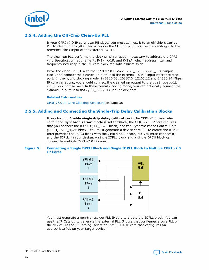
2.5.4. Adding the Off-Chip Clean-Up PLL
If your CPRI v7.0 IP core is an RE slave, you must connect it to an off-chip clean-upPLL to clean up any jitter that occurs in the CDR output clock, before sending it to thereference clock input of the external TX PLL.
The clean-up PLL performs the clock synchronization necessary to address the CPRIv7.0 Specification requirements R-17, R-18, and R-18A, which address jitter andfrequency accuracy in the RE core clock for radio transmission.
Drive the clean-up PLL with the CPRI v7.0 IP core xcvr_recovered_clk outputclock, and connect the cleaned up output to the external TX PLL input reference clockport. In the hybrid clocking mode, in 8110.08, 10137.6, 12165.12 and 24330.24 MbpsIP core variations, you should connect the cleaned up output to the cpri_coreclkinput clock port as well. In the external clocking mode, you can optionally connect thecleaned up output to the cpri_coreclk input clock port.
Related Information
CPRI v7.0 IP Core Clocking Structure on page 38
2.5.5. Adding and Connecting the Single-Trip Delay Calibration Blocks
If you turn on Enable single-trip delay calibration in the CPRI v7.0 parametereditor, and Synchronization mode is set to Slave, the CPRI v7.0 IP core requiresthat you connect the IOPLL (pll_core block) and the Dynamic Phase Control Unit(DPCU) (pll_dpcu block). You must generate a device core PLL to create the IOPLL.Intel provides the DPCU block with the CPRI v7.0 IP core, but you must connect it,and the IOPLL, in your design. A single IOPLL block and a single DPCU block canconnect to multiple CPRI v7.0 IP cores.
Figure 5. Connecting a Single DPCU Block and Single IOPLL Block to Multiple CPRI v7.0IP Cores
CPRI v7.0IP Core
1
DPCUBlock
IOPLLBlock
CPRI v7.0IP Core
2
CPRI v7.0IP Core
3
You must generate a non-transceiver PLL IP core to create the IOPLL block. You canuse the IP Catalog to generate the external PLL IP core that configures a core PLL onthe device. In the IP Catalog, select an Intel FPGA IP core that configures anappropriate PLL on your target device.
2. Getting Started with the CPRI v7.0 IP Core
UG-20008 | 2019.02.06
CPRI v7.0 IP Core User Guide Send Feedback
30
For your Intel Arria 10 design, you must select Arria 10 FPLL in the IP Catalog. Inthe parameter editor for the fPLL IP core, you must set the following parametervalues:
• Set fPLL Mode to Core.
• Set the PLL output frequency to the expected input frequency for the CPRI v7.0 IPcore cpri_coreclk input signal.
• Turn on Enable access to dynamic phase shift ports.
You must connect the IOPLL and DPCU signals to the CPRI v7.0 IP core signalsaccording to the following rules. Refer to Example CPRI v7.0 Clock Connections inDifferent Clocking Modes on page 41 for an illustration of the clock connections.
Table 15. Required Connections to and From IOPLL Block in CPRI v7.0 Design WithSingle-Trip Delay Calibration
IOPLL Block Signal Connect to
cntsel (input) DPCU pll_cntsel output signal
num_phase_shifts (input) DPCU pll_num_phase_shifts output signal
outclk_0 (output) CPRI v7.0 IP core cpri_coreclk input clock signal
phase_done (output) DPCU pll_phase_done input signal
phase_en (input) DPCU pll_phase_en output signal
refclk (input) CPRI v7.0 IP core tx_clkout output signal or output fromthe off-chip clean-up PLL
rst (input) Drive with the inverse of the CPRI v7.0 IP core reset_ninput signal
scanclk (input) DPCU pll_scanclk output signal
updn (input) DPCU pll_updn output signal
Table 16. Required Connections to and From DPCU Block in CPRI v7.0 Design WithSingle-Trip Delay Calibration
DPCU Block Signal Connect to
clk Drive in the frequency range of 100–150 MHz.Note: Intel recommends that you drive this DPCU input
clock with the source for the reconfig_clk.
reset_n (input) CPRI v7.0 IP core reset_n input signal
csr_bit_rate (input) If you turned on Enable line bit rate auto-negotiation inthe CPRI v7.0 parameter editor, connect to the CPRI v7.0 IPcore nego_bitrate_out[4:0] output signal.If autorate negotiation is not turned on, hardwire the DPCUcsr_bit_rate signal to the encoded value for the CPRIline bit rate:• 6'b000001: 0.6144 Gbps• 6'b000010: 1.2288 Gbps• 6'b000100: 2.4576 Gbps• 6'b000101: 3.0720 Gbps• 6'b001000: 4.9150 Gbps• 6'b001010: 6.1440 Gbps• 6'b010110: 8.11008 Gbps
continued...
2. Getting Started with the CPRI v7.0 IP Core
UG-20008 | 2019.02.06
Send Feedback CPRI v7.0 IP Core User Guide
31

DPCU Block Signal Connect to
• 6'b010000: 9.8304 Gbps• 6'b010100: 10.1376 Gbps• 6b'011000: 12.16512 Gbps• 6'b110000 : 24.33024 Gbps
cal_status (output) CPRI v7.0 IP core cal_status input signal
cal_ctrl (input) CPRI v7.0 IP core cal_ctrl output signal
pll_cntsel (output) IOPLL cntsel input signal
pll_num_phase_shifts (output) IOPLL num_phase_shifts input signal
pll_phase_done (input) IOPLL phase_done output signal
pll_phase_en (output) IOPLL phase_en input signal
pll_scanclk (output) IOPLL scanclk input signal
pll_updn (output) IOPLL updn input signal
User logic must provide the connections.
2.6. Simulating Intel FPGA IP Cores
The Intel Quartus Prime software supports RTL- and gate-level design simulation ofIntel FPGA IP cores in supported EDA simulators. Simulation involves setting up yoursimulator working environment, compiling simulation model libraries, and runningyour simulation.
You can use the functional simulation model and the testbench or example designgenerated with your IP core for simulation. The IP generation output also includesscripts to compile and run any testbench. For a complete list of models or librariesrequired to simulate your IP core, refer to the scripts generated with the testbench.
Related Information
• Simulating Intel FPGA IP Cores
• Simulating Altera FPGA Designs chapter in Quartus Prime Standard EditionHandbook, Volume 3: Verification
• Simulating Intel FPGA Designs chapter in Intel Quartus Prime Pro EditionHandbook, Volume 3: Verification
2.7. Understanding the Testbench
Intel provides a demonstration testbench with the CPRI v7.0 IP core.
If you click Generate Example Design in the CPRI v7.0 parameter editor for IntelArria 10, and Intel Stratix 10 device variations, the Quartus Prime software generatesthe demonstration testbench. The parameter editor prompts you for the desiredlocation of the testbench. For V-series device variations, you click Finish to generatethe design example in Intel Quartus Prime Standard Edition software.
2. Getting Started with the CPRI v7.0 IP Core
UG-20008 | 2019.02.06
CPRI v7.0 IP Core User Guide Send Feedback
32

The testbench performs the following sequence of actions with the static DUT
1. Enables transmission on the CPRI link by setting the tx_enable bit (bit [0]) ofthe CPRI IP core L1_CONFIG register at offset 0x8 (and resetting all other fields ofthe register)>
2. Configures the DUT at the highest possible HDLC bit rate for the CPRI line bit rate,by setting the tx_slow_cm_rate field of the CPRI CM_CONFIG register at offset0x1C to the appropriate value.
3. Reads the CM_CONFIG register to confirm settings.
4. After the DUT and the testbench achieve frame synchronization, executes thefollowing transactions (Only when you turn on corresponding interface in IPparameter editor):
a. Performs several write transactions to the AUX Tx interface and confirms thetestbench receives them on the CPRI link.
b. Performs several write transactions to the VS interface and confirms thetestbench receives them from the DUT on the CPRI link.
c. Performs several write transactions to the RTVS interface for the 10G variant,and confirms the testbench receives them form the DUT on the CPRI link.
d. Performs several write transactions to the Ctrl_AxC interface and confirms thetestbench receives them from the DUT on the CPRI link.
e. Performs several HDLC transactions and confirms the testbench receives themfrom the DUT on the CPRI link.
f. Performs several write transactions to the MI or GMI interface and confirmsthe testbench receives them from the DUT on the CPRI link.
2.8. Running the Testbench
To run the CPRI v7.0 IP core demonstration testbench, follow these steps.
1. In the Quartus Prime software IP Catalog, select the CPRI v7.0 IP core and clickAdd.
2. When prompted, you can specify any output file type (HDL). This setting isrelevant only for synthesis and does not impact simulation of the demonstrationtestbench.
3. In the CPRI v7.0 parameter editor, set the following parameter values:
Table 17. CPRI v7.0 IP Core Variation for Demonstration TestbenchThe testbench scripts require that you set these values in the CPRI v7.0 parameter editor before you clickGenerate Example Design. The scripts generate the DUT but they require that you provide the parametervalues.
Parameter Value
Line bit rate (Mbit/s) Any value the device family supports.
Synchronization mode Master
Operation mode Any available mode
Transmitter local clock division factor 1
Number of receiver CDR reference clock(s) 1
continued...
2. Getting Started with the CPRI v7.0 IP Core
UG-20008 | 2019.02.06
Send Feedback CPRI v7.0 IP Core User Guide
33

Parameter Value
Receiver CDR reference clock frequency (MHz) 253.44 if the Line bit rate is 8.11008 or 10.1376 or12.16512 Gbps and the IP core targets the Intel Stratix 10device family368.64 if the Line bit rate is 24.33024 Gbps and the IP coretargets the Intel Stratix 10 device family253.44 if the Line bit rate is 8.11008 or 10.1376 Gbps andthe IP core targets the Intel Arria 10 device family253.44 if the Line bit rate is 8.11008 or 10.1376 Gbps andthe IP core targets a 28-nm device family253.44 if the Line bit rate is 8.11008 Gbps and the IP coretargets Arria V GZ device family307.2 for all other cases
Core clock source input Internal or External
Recovered clock source PMA if the Line bit rate is 10.1376 Gbps and IP core targetsthe Stratix V device family; PCS otherwise
Receiver soft buffer depth (value shown is log2 of actualdepth)
6
Enable line bit rate auto-negotiation Turn off
Enable line bit rate auto-negotiation down to 614.4 Mbps Not available
Management (CSR) interface standard Avalon-MM
Avalon-MM interface addressing type Word
Auxiliary and direct interfaces write latency cycle(s) 0
Enable auxiliary interface Turn on or Turn off
Enable all control word access via management interface Turn off
Enable direct Z.130.0 alarm bits access interface Turn off
Enable direct ctrl_axc access interface Turn on or Turn off
Enable direct vendor specific access interface Turn on or Turn off
Enable direct real-time vendor specific interface Turn on or Turn off
Enable start-up sequence state machine Turn off
Enable protocol version and C&M channel setting auto-negotiation
Not available
Enable direct IQ mapping interface Turn on or Turn off
Enable HDLC serial interface Turn on or Turn off
Ethernet PCS interface NONE, MII or GMII
L2 Ethernet PCS Tx/Rx FIFO depth (value shown is log2 ofactual depth)
8
Enable L1 debug interfaces Turn off
Enable ADME, transceiver capability, control and statusregisters access
Turn off
Enable transceiver PMA serial forward loopback path Turn off
Enable parallel forward loopback paths Turn off
Enable parallel reversed loopback paths Turn off
Enable single-trip delay calibration Not available
continued...
2. Getting Started with the CPRI v7.0 IP Core
UG-20008 | 2019.02.06
CPRI v7.0 IP Core User Guide Send Feedback
34

Parameter Value
Enable round-trip delay calibration Turn off
Round-trip delay calibration FIFO depth Not available
Language for top-level simulation file • Verilog• VHDL
4. For Intel Stratix 10 and Intel Arria 10 device variations, click the GenerateExample Design button in the CPRI v7.0 parameter editor button and specify thedesired location of the testbench. For V-series device variations, click Finishbutton and leave the Generate Example Design checked in Intel Quartus PrimeStandard Edition software. In this case, you don't have a choice to specify desiredlocation of the testbench. The IP saves the design example in the followinglocation: <your_ip>_testbench/altera_cpri_ii/.
5. For Intel Stratix 10 and Intel Arria 10 device variations, change directory to<your_ip>/setup_scripts/<simulator_vendor>. For V-series devicevariations, change directory to <your_ip>_testbench/altera_cpri_ii/setup_scripts/<simulator_vendor>.
6. If you are using a simulator that requires that you open a user interface, openyour target simulator.
Note: You must select a simulator that is supported by the Intel Quartus Primesoftware version you are using.
7. Execute the simulation script available for your simulation in the directory.
• In the Mentor Graphics ModelSim simulator, type do msim_commands.do
8. You can modify testbench parameters from a file params_list.sv, located at<your_ip>/testbench location for Intel Stratix 10 and Intel Arria 10 devicevariations. You can find this file at <your_ip>_testbench/altera_cpri_ii/testbench location for V-series device variations.
2.9. Compiling the Full Design and Programming the FPGA
You can use the Start Compilation command on the Processing menu in the IntelQuartus Prime software to compile your design. After successfully compiling yourdesign, program the targeted Intel FPGA with the Programmer and verify the design inhardware.
Note: The IP core directory includes a Synopsys Constraint (.sdc) file at <IP core instancedirectory>/altera_cpri_ii_instance_<Intel Quartus Prime release>/synth/altera_cpri.sdc.
Related Information
• Incremental Compilation for Hierarchical and Team-Based Design
• Programming Intel FPGA Devices: Intel Quartus Prime Standard Edition Software
• Programming Intel FPGA Devices: Intel Quartus Prime Pro Edition Software
2. Getting Started with the CPRI v7.0 IP Core
UG-20008 | 2019.02.06
Send Feedback CPRI v7.0 IP Core User Guide
35

3. Functional DescriptionThe CPRI v7.0 IP core implements Layer 1 of the CPRI v7.0 specification and providesoptional CPRI v7.0 Layer 2 access points through various interfaces.
3.1. Interfaces Overview
Figure 6. CPRI v7.0 IP Core InterfacesThe IP core assembles the outbound CPRI frame control words and data from all of these interfaces, andunloads and routes control words and data from the inbound CPRI frame to the appropriate interfaces, basedon configuration and register settings. With parameter settings, you control the presence or absence of theAUX interface, the L1 control and status interface, and each of the interfaces that provide dedicated access tospecific parts of the CPRI frame. In contrast, the CPRI interface, the transceiver interfaces, and the softwareinterface to the IP core registers are always implemented.
L1
xcvr_txdataout
RegistersL1
InbandSlowC&M
FastC&M
VendorSpecific
L1Control and Status
Interface
VSSInterface
Interfaceto Reset Controllers
STDCalibration
InterfaceInterface
to TX PLL
Transmitter
xcvr_rxdatain
CPRI Interface (CPRI Link)
Receiver
Multiplexing
Access to Ctrl_AxC bytesin CPRI frame
Access to IQ Data
in CPRI frame
Full accessto
CPRI frame
Real-TimeVendorSpecific
HDLCSerial
EthernetPCS
Ctrl_AxCInterface
RTVSInterface
Direct IQInterface
TransceiverReconfiguration
Interface
Dedicated access to specific parts of CPRI frame
AUXInterface
MII / GMII SoftwareInterface
UG-20008 | 2019.02.06
Send Feedback
Intel Corporation. All rights reserved. Intel, the Intel logo, Altera, Arria, Cyclone, Enpirion, MAX, Nios, Quartusand Stratix words and logos are trademarks of Intel Corporation or its subsidiaries in the U.S. and/or othercountries. Intel warrants performance of its FPGA and semiconductor products to current specifications inaccordance with Intel's standard warranty, but reserves the right to make changes to any products and servicesat any time without notice. Intel assumes no responsibility or liability arising out of the application or use of anyinformation, product, or service described herein except as expressly agreed to in writing by Intel. Intelcustomers are advised to obtain the latest version of device specifications before relying on any publishedinformation and before placing orders for products or services.*Other names and brands may be claimed as the property of others.
ISO9001:2015Registered

Multiple interfaces control the contents of the outbound CPRI frame control words anddata. The CPRI v7.0 implements the following transmission priorities among theseinterfaces:
• CPRI frame control words:
1. If the IP core implements the AUX interface, the AUX interface aux_tx_databus, with appropriate delay, has first priority in filling in the outbound CPRIframe control words.
2. If the IP core does not implement the AUX interface, or the aux_tx_maskvalue associated with the relevant incoming data blocks the relevantaux_tx_data bits, each of the following interfaces, if implemented, hassecondary priority in filling the relevant part of the outbound CPRI framecontrol words:
— Real-time vendor specific interface (RTVS)
— Vendor specific interface (VS)
— AxC control information interface (Ctrl_AxC)
3. For any part of the CPRI frame control words not filled in by one of theprevious methods, the transmission-enabled values most recently written tothe control transmit table through the full control word access registersCTRL_INDEX and TX_CTRL determine the contents of the outbound CPRIframe control words. If the most recently written word for a CPRI frameposition is not transmission-enabled, no transmission is authorized from thecontrol transmit table to that CPRI frame position.
4. If none of the previous methods provides the content for a position in the CPRIframe control word, the following interfaces, if implemented, have the lowestpriority in filling the relevant part of the outbound CPRI frame control words:
— Fast control and management (Ethernet) MII or GMII interface
— Slow control and management (HDLC) serial interface
— L1 control and status interface
— Dedicated registers that contain or control content for control wordpositions in the CPRI frame. For example, the rx_prot_ver_filter fieldof the PROT_VER register
— Transmission of special symbols according to the CPRI protocol. Forexample, K28.5, D16.2, /S/, or /T/
• CPRI frame I/Q data words:
1. If the IP core implements the AUX interface, the AUX interface aux_tx_databus, with appropriate delay, has first priority in filling in the outbound CPRIframe I/Q data words.
2. If the IP core does not implement the AUX interface, or the aux_tx_maskvalue associated with the relevant incoming data blocks the relevantaux_tx_data bits, the Direct I/Q interface, if implemented, has secondarypriority in filling the relevant part of the outbound CPRI frame I/Q data words.
3. Functional Description
UG-20008 | 2019.02.06
Send Feedback CPRI v7.0 IP Core User Guide
37

3.2. CPRI v7.0 IP Core Clocking Structure
Figure 7. CPRI v7.0 IP Core Clocking StructureIllustrates the clocks and clock domains in the CPRI v7.0 IP core. Clock domains shown are cpri_clkout,clk_ex_delay, cpu_clk, and mii_{rx,tx}clk. The external clean-up PLL is only required in slave clockingmode. The tx_clkout is only available in external clocking mode, and the xcvr_recovered_clk is onlyavailable in slave clocking mode.
TX PLL
Standard TX PCS
10G TX PCS
TXPMA
Standard RX PCS
10G RX PCS
RXPMA
Native PHY IP Core
CPRI v7.0 IP Core
cpu_clk
mii_rxclkmii_txclk
clk_ex_delaytx_clkout cpri_coreclk
reconfig_clk
xcvr_ext_pll_clk
xcvr_recovered_clk
xcvr_cdr_refclk
cpri_clkoutExternal Clean-Up PLL(in slave mode only)
CPU InterfaceExtended Delay Measurem
ent
MII
FIFO
FIFO
The main CPRI v7.0 IP core clock is cpri_clkout.
Table 18. CPRI v7.0 IP Core Input Clocks
CPRI v7.0 Input Clock Information
xcvr_ext_pll_clk Clocks the transmitter PMA.You should drive this input clock with the output of the external TX PLL. The frequencyof this clock must be one half of the CPRI line bit rate, multiplied by the local clockdivision factor. You must configure a PLL IP core that is capable of driving the requiredfrequency.
xcvr_cdr_refclk orxcvr_cdr_refclk[1:0]
Receiver CDR reference clock. You must drive this clock at the frequency you specifiedfor the Receiver CDR reference clock frequency (MHz) parameter in the CPRI v7.0parameter editor.If you set the Number of receiver CDR reference clock(s) parameter in the CPRIv7.0 parameter editor to the value of 2, this clock is two bits wide.In the case of a two-bit xcvr_cdr_refclk port, drive xcvr_cdr_refclk[0] with thereference clock for the initial CPRI line bit rate, because by default, this is the clocksignal that drives the CDR.The IP core supports all CDR reference clock frequencies available in the drop-downmenu for the Receiver CDR reference clock frequency (MHz) parameter.
reconfig_clk In Arria V, Arria V GZ, Cyclone V, and Stratix V variations, clock for CPRI v7.0 IP coretransceiver start-up and reconfiguration.In Intel Arria 10 and Intel Stratix 10 variations, clocks the signals on the CPRI v7.0transceiver reconfiguration interface. In these variations, this clock is not present if youturn off all of Enable start-up sequence state machine, Enable ADME, transceivercapability, control and status registers access, and parameters only available inIntel Arria 10 variations, Enable line bit rate auto-negotiation, Enable single-tripdelay calibration.
continued...
3. Functional Description
UG-20008 | 2019.02.06
CPRI v7.0 IP Core User Guide Send Feedback
38

CPRI v7.0 Input Clock Information
In variations that target any other supported device family, this clock is not present ifyou turn off both Enable line bit rate auto-negotiation, Enable start-up sequencestate machine.The supported frequency range of this clock is 100–150 MHz.
ex_delay_clk Clock for extended delay measurement.
latency_sclk Clock for delay measurement through the Intel Stratix 10 hard FIFO buffers in the PCSand the core. You can (but need not) drive this clock at the same frequency asex_delay_clk. This clock is present only in IP cores that target an Intel Stratix 10device.
cpri_coreclk In hybrid clocking mode, this clock drives the CPRI v7.0 IP core clock cpri_clkoutwhen the IP core is running at the CPRI line bit rate of 8.11008, 10.1376, 12.16512 or24.33024 Gbps and a clock from the transceiver PHY drives the cpri_clkout at allother rates. In external clocking mode, cpri_coreclk drives cpri_clkout at all CPRIline rates. In internal clocking mode, the clock from transceiver PHY drivescpri_clkout.The frequency at which you must drive cpri_coreclk depends on the CPRI line bitrate:
CPRI Line Bit Rate cpri_coreclk Frequency
0.6144 Gbps 15.36 MHz
1.2288 Gbps 30.72 MHz
2.4576 Gbps 61.44 MHz
3.0720 Gbps 76.80 MHz
4.9152 Gbps 122.88 MHz
6.1440 Gbps 153.60 MHz
8.11008 Gbps 245.76 MHz
9.8304 Gbps 245.76 MHz
10.1376 Gbps 307.20 MHz
12.16512 Gbps 184.32 MHz
24.33024 Gbps 368.64 MHz
You must drive this clock from the same clock source as the xcvr_ext_pll_clk inputsignal to the IP core.
cpu_clk Clocks the signals on the CPRI v7.0 CPU interface. Supports any frequency that thedevice fabric supports.
mii_txclk mii_txclk clocks the MII transmitter interface and mii_rxclk clocks the MII receiverinterface. You must drive these clocks at the frequency of 25 MHz/2.5 MHz to achievethe 100 Mbps/10 Mbps bandwidth required for this interface.These clocks are present only if you set the value of Ethernet PCS interface to thevalue of MII in the CPRI v7.0 parameter editor.
mii_rxclk
gmii_txclk gmii_txclk clocks the GMII transmitter interface and gmii_rxclk clocks the GMIIreceiver interface. You must drive these clocks at the frequency of 125 MHz to achievethe 1000 Mbps bandwidth required for this interface.These clocks are present only if you set the value of Ethernet PCS interface to thevalue of GMII in the CPRI v7.0 parameter editor.
gmii_rxclk
3. Functional Description
UG-20008 | 2019.02.06
Send Feedback CPRI v7.0 IP Core User Guide
39

Table 19. CPRI v7.0 IP Core Output Clocks
CPRI v7.0 Output Clock Information
cpri_clkout Master clock for the CPRI v7.0 IP core. In hybrid clocking mode, when the IP core isrunning at the CPRI line bit rate of 8.11008, 10.1376, 12.16512 or 24.33024 Gbps, thecpri_coreclk input clock drives cpri_clkout. At all other CPRI line bit rates, the TxPCS drives cpri_clkout.In internal clocking mode, the TX PCS drives the cpri_clkoutI at all CPRI line bitrates.In external clocking mode, the cpri_coreclk input clock drives cpri_clkout at allCPRI line bit rates.The frequency of cpri_clkout depends on the CPRI line bit rate:
CPRI Line Bit Rate cpri_clkout Frequency
0.6144 Gbps 15.36 MHz
1.2288 Gbps 30.72 MHz
2.4576 Gbps 61.44 MHz
3.0720 Gbps 76.80 MHz
4.9152 Gbps 122.88 MHz
6.1440 Gbps 153.60 MHz
8.11008 Gbps 245.76 MHz
9.8304 Gbps 245.76 MHz
10.1376 Gbps 307.20 MHz
12.16512 Gbps 184.32 MHz
24.33024 Gbps 368.64 MHz
xcvr_recovered_clk Direct recovered clock from the receiver CDR. Use this output clock to drive the externalclean-up PLL when your IP core is in slave mode.The IP core drives this clock from the PCS or the PMA block of the transceiver,depending on the value you set for the Recovered clock source parameter in the CPRIv7.0 parameter editor.This clock is present only in CPRI v7.0 IP cores in slave clocking mode that support RXtraffic. (This clock is not present in CPRI v7.0 IP cores with Operation mode set to thevalue of TX simplex).The frequency of recovered clock speed (xcvr_recovered_clk) depends on the CPRIline bit rate.
CPRI Line Bit Rate cpri_clkout Frequency
0.6144 Gbps 15.36 MHz
1.2288 Gbps 30.72 MHz
2.4576 Gbps 61.44 MHz
3.0720 Gbps 76.80 MHz
4.9152 Gbps 122.88 MHz
6.1440 Gbps 153.60 MHz
8.11008 Gbps 220.75 MHz
9.8304 Gbps 245.76 MHz
continued...
3. Functional Description
UG-20008 | 2019.02.06
CPRI v7.0 IP Core User Guide Send Feedback
40
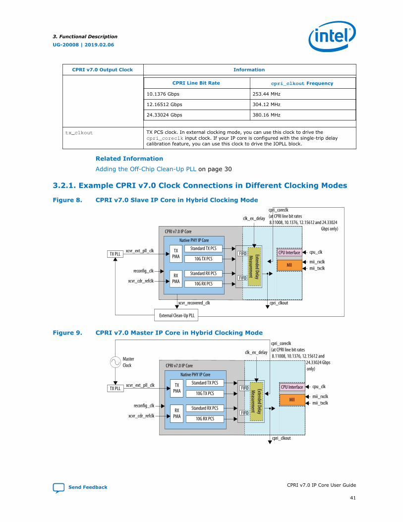
CPRI v7.0 Output Clock Information
CPRI Line Bit Rate cpri_clkout Frequency
10.1376 Gbps 253.44 MHz
12.16512 Gbps 304.12 MHz
24.33024 Gbps 380.16 MHz
tx_clkout TX PCS clock. In external clocking mode, you can use this clock to drive thecpri_coreclk input clock. If your IP core is configured with the single-trip delaycalibration feature, you can use this clock to drive the IOPLL block.
Related Information
Adding the Off-Chip Clean-Up PLL on page 30
3.2.1. Example CPRI v7.0 Clock Connections in Different Clocking Modes
Figure 8. CPRI v7.0 Slave IP Core in Hybrid Clocking Mode
TX PLLStandard TX PCS
10G TX PCS
TXPMA
Standard RX PCS
10G RX PCS
RXPMA
Native PHY IP Core
CPRI v7.0 IP Core
cpu_clk
mii_rxclkmii_txclk
clk_ex_delay
cpri_coreclk(at CPRI line bit rates 8.11008, 10.1376, 12.15612 and 24.33024 Gbps only)
reconfig_clk
xcvr_ext_pll_clk
xcvr_recovered_clk
xcvr_cdr_refclk
cpri_clkout
External Clean-Up PLL
CPU InterfaceExtended DelayM
easurement
MII
FIFO
FIFO
Figure 9. CPRI v7.0 Master IP Core in Hybrid Clocking Mode
TX PLLStandard TX PCS
10G TX PCS
TXPMA
Standard RX PCS
10G RX PCS
RXPMA
Native PHY IP Core
CPRI v7.0 IP Core
cpu_clk
mii_rxclkmii_txclk
clk_ex_delay
cpri_coreclk(at CPRI line bit rates 8.11008, 10.1376, 12.15612 and 24.33024 Gbps only)
reconfig_clk
xcvr_ext_pll_clk
xcvr_cdr_refclk
cpri_clkout
CPU InterfaceExtended DelayM
easurement
MII
FIFO
FIFO
MasterClock
3. Functional Description
UG-20008 | 2019.02.06
Send Feedback CPRI v7.0 IP Core User Guide
41

Figure 10. CPRI v7.0 Master IP Core in Internal Clocking Mode
TX PLLStandard TX PCS
10G TX PCS
TXPMA
Standard RX PCS
10G RX PCS
RXPMA
Native PHY IP Core
CPRI v7.0 IP Core
cpu_clk
mii_rxclkmii_txclk
clk_ex_delay
reconfig_clk
xcvr_ext_pll_clk
xcvr_cdr_refclk
cpri_clkout
CPU InterfaceExtended DelayM
easurement
MII
FIFO
FIFO
MasterClock
Figure 11. CPRI v7.0 Slave IP Core in Internal Clocking Mode
TX PLLStandard TX PCS
10G TX PCS
TXPMA
Standard RX PCS
10G RX PCS
RXPMA
Native PHY IP Core
CPRI v7.0 IP Core
cpu_clk
mii_rxclkmii_txclk
clk_ex_delay
reconfig_clk
xcvr_ext_pll_clk
xcvr_recovered_clk
xcvr_cdr_refclk
cpri_clkout
External Clean-Up PLL
CPU InterfaceExtended DelayM
easurement
MII
FIFO
FIFO
3. Functional Description
UG-20008 | 2019.02.06
CPRI v7.0 IP Core User Guide Send Feedback
42

Figure 12. CPRI v7.0 Slave IP Core in External Clocking Mode
TX PLLStandard TX PCS
10G TX PCS
TXPMA
Standard RX PCS
10G RX PCS
RXPMA
Native PHY IP Core
CPRI v7.0 IP Core
cpu_clk
mii_rxclkmii_txclk
clk_ex_delay
cpri_coreclk
reconfig_clk
xcvr_ext_pll_clk
xcvr_recovered_clk
xcvr_cdr_refclk
cpri_clkout
External Clean-Up PLL
CPU InterfaceExtended DelayM
easurement
MII
FIFO
FIFO
tx_clkout
or
Figure 13. CPRI v7.0 Master IP Core in External Clocking Mode
TX PLLStandard TX PCS
10G TX PCS
TXPMA
Standard RX PCS
10G RX PCS
RXPMA
Native PHY IP Core
CPRI v7.0 IP Core
cpu_clk
mii_rxclkmii_txclk
clk_ex_delaytx_clkout
cpri_coreclk
reconfig_clk
xcvr_ext_pll_clk
xcvr_cdr_refclk
cpri_clkout
CPU InterfaceExtended DelayM
easurement
MII
FIFO
FIFO
MasterClock
or
3. Functional Description
UG-20008 | 2019.02.06
Send Feedback CPRI v7.0 IP Core User Guide
43

Figure 14. CPRI v7.0 Slave IP Core in External Clocking Mode with Single-Trip DelayCalibration FeatureIntel provides the IOPLL and DPCU blocks with the CPRI v7.0 IP core. For correct single-trip delay calibrationfunctionality, you must connect these blocks as shown.
TX PLLStandard TX PCS
10G TX PCS
TXPMA
Standard RX PCS
10G RX PCS
RXPMA
Native PHY IP Core
CPRI v6.0 IP Core
cpu_clk
mii_rxclkmii_txclk
clk_ex_delaycpri_coreclk
reconfig_clk
xcvr_ext_pll_clk
xcvr_recovered_clk
xcvr_cdr_refclk
cpri_clkout
External Clean-Up PLL
CPU InterfaceExtended DelayM
easurement
MII
FIFO
FIFO
tx_clkout
IOPLL DPCU
CalibrationInterface
or
3.3. CPRI v7.0 IP Core Reset Requirements
To reset the entire CPRI v7.0 IP core, you must assert the reset signals to the IP coreand to the required external reset controller logic. The external reset controller logicresets only the transceiver. If you instantiate a duplex CPRI v7.0 IP core, you mustinstantiate two PHY Reset Controllers to implement this logic, one for the TX data pathand one for the RX data path. The two reset signals reset_tx_n and reset_rx_neach cause the reset logic to reset the relevant data path of the IP core. If youconnect these two reset signals to the corresponding PHY Reset Controllers, each onealso causes the transceiver in that data path to reset.
In the case of a duplex CPRI v7.0 IP core, you can assert the reset_n signal insteadof asserting the two reset signals reset_tx_n and reset_rx_n. However, unlessyou also connect the reset_n signal to the external reset controllers, the transceiversdo not reset in this case.
In addition, some individual interfaces to the IP core have their own reset signals toreset only the associated interface and logic.
Table 20. CPRI v7.0 IP Core Reset Signals
You can assert all reset signals asynchronously to any clock. However, you must hold each reset signal assertedfor one full clock period of its associated clock, to ensure it is captured by the IP core.
CPRI v7.0 IP Core Reset Signal Polarity AssociatedClock
Information
xcvr_tx_analogreset Active high — Analog reset to transmitter from external resetcontroller.
xcvr_tx_digitalreset Active high — Digital reset to transmitter from external resetcontroller.
continued...
3. Functional Description
UG-20008 | 2019.02.06
CPRI v7.0 IP Core User Guide Send Feedback
44

CPRI v7.0 IP Core Reset Signal Polarity AssociatedClock
Information
xcvr_rx_analogreset Active high — Analog reset to receiver from external resetcontroller.
xcvr_rx_digitalreset Active high — Digital reset to receiver from external resetcontroller.
reset_n Active low
reconfig_clk
Asynchronous global reset signal. Resets the IPcore soft logic. This signal does not reset the CSRregisters, the extended delay measurementsettings, or the transceivers.To reset the CSR registers, you must assert thecpu_reset_n signal. To reset the extendeddelay measurement settings, you must assertthe ex_delay_reset_n signal.To reset the transceiver you must drive the resetinput port of the required PHY Reset Controllers.
reset_tx_n Active low
reconfig_clk
Asynchronous global reset signal that resets theTX path of the CPRI v7.0 IP core. Resets the IPcore soft logic. To reset the transceiver you mustdrive the reset input port of the required PHYReset Controller.
reset_rx_n Active low
reconfig_clk
Asynchronous global reset signal that resets theRX path of the CPRI v7.0 IP core. Resets the IPcore soft logic. To reset the transceiver you mustdrive the reset input port of the required PHYReset Controller.
ex_delay_reset_n Active low ex_delay_clk
Resets the extended delay measurement block.
latency_sreset_n Active low latency_sclk
Resets the Intel Stratix 10 hard FIFO delaymeasurement soft logic.
reconfig_reset Active high reconfig_clk Asynchronous reset signal. Resets the CPRI v7.0Intel Arria 10 or Intel Stratix 10 transceiverreconfiguration interface and all of the registersto which it provides access.In IP cores that target a 28-nm device, thissignal is involved in rate switching and auto-ratenegotiation.In Intel Arria 10 and Intel Stratix 10 variations,this signal is not present if you turn off all ofEnable start-up sequence state machine,Enable ADME, transceiver capability, controland status registers access, and parametersonly available in Intel Arria 10 variations, Enableline bit rate auto-negotiation, Enable single-trip delay calibration.In variations that target other devices, this signalis not present if you turn off all of Enable linebit rate auto-negotiation, Enable start-upsequence state machine.
cpu_reset_n Active low cpu_clk Resets the CPRI v7.0 CPU interface and all of theregisters to which it provides access.
mii_txreset_n Active low mii_txclk Resets the MII transmitter interface and FIFOwrite logic.
continued...
3. Functional Description
UG-20008 | 2019.02.06
Send Feedback CPRI v7.0 IP Core User Guide
45
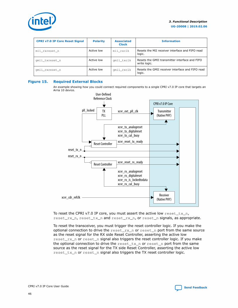
CPRI v7.0 IP Core Reset Signal Polarity AssociatedClock
Information
mii_rxreset_n Active low mii_rxclk Resets the MII receiver interface and FIFO readlogic.
gmii_txreset_n Active low gmii_txclk Resets the GMII transmitter interface and FIFOwrite logic.
gmii_rxreset_n Active low gmii_rxclk Resets the GMII receiver interface and FIFO readlogic.
Figure 15. Required External BlocksAn example showing how you could connect required components to a single CPRI v7.0 IP core that targets anArria 10 device.
Reset Controller
Reset Controller
TXPLL
Transmitter(Native PHY)
Receiver(Native PHY)
User-DefinedReference Clock
xcvr_ext_pll_clk
xcvr_tx_analogresetxcvr_tx_digitalresetxcvr_tx_cal_busy
xcvr_rx_analogresetxcvr_rx_digitalresetxcvr_rx_is_lockedtodataxcvr_rx_cal_busy
xcvr_cdr_refclk
reset_tx_n
reset_rx_n
pll_locked
CPRI v7.0 IP Core
xcvr_reset_tx_ready
xcvr_reset_rx_ready
To reset the CPRI v7.0 IP core, you must assert the active low reset_tx_n,reset_rx_n, reset_tx_n and reset_rx_n, or reset_n signals, as appropriate.
To reset the transceiver, you must trigger the reset controller logic. If you make theoptional connection to drive the reset_rx_n or reset_n port from the same sourceas the reset signal for the RX side Reset Controller, asserting the active lowreset_rx_n or reset_n signal also triggers the reset controller logic. If you makethe optional connection to drive the reset_tx_n or reset_n port from the samesource as the reset signal for the TX side Reset Controller, asserting the active lowreset_tx_n or reset_n signal also triggers the TX reset controller logic.
3. Functional Description
UG-20008 | 2019.02.06
CPRI v7.0 IP Core User Guide Send Feedback
46

When you trigger the reset controllers, they should deassert thexcvr_reset_tx_ready and xcvr_reset_rx_ready input ready signals to the IPcore. After each reset controller completes resetting the transceiver and IP core datapath, it should assert the relevant ready signal.
Related Information
Integrating Your IP Core in Your Design: Required External Blocks on page 24Shows main data path reset signals and how the reset controller connects to the IPcore.
3.4. Start-Up Sequence Following Reset
After reset, if you turned on Enable start-up sequence state machine in the CPRIv7.0 IP core, the internal state machine performs link synchronization and otherinitialization tasks. If you did not turn on Enable start-up sequence state machine,user logic should perform these functions.
Figure 16. Start-up states and transitions Figure From CPRI v7.0 Specification With IPCore AdditionsStates and transitions marked in black are from the CPRI v7.0 specification Figure 30: Start-up states andtransitions. Additional transitions from State G that the IP core implements are marked in blue.
Standby
A
Interface and Vendor-Specific Negotiation
E
L1 Synchronization
B
Protocol Setup
C
C/M Plane (L2+)Setup
D
Operation
F
1
2
3
4
6
5
7
Passive Link
G
No C&M
C&MProposed
15
14
C/M PlaneDisconnected
8
Reconfiguration 9
REC/RE Shutdown orRE Reset from Any State
L1 LOS/LOF/Received RAI
11
10
C&M Speed Mismatchfrom State E, F
Protocol Mismatchfrom State D, E, F, G
Protocol Mismatch13
12
L1 Start-Up Timer Expired
L1 Start-Up Timer Expired
16
reconfig_reset
LOS/LOF/RAI/
3. Functional Description
UG-20008 | 2019.02.06
Send Feedback CPRI v7.0 IP Core User Guide
47

The internal state machine implements the start-up state machine transitions shownin section 4.5.2, Figure 30: Start-up states and transitions, and described in section4.5.3, in the CPRI specification. In addition, the internal state machine implements thefollowing transitions from State G: Passive Link.
• If you assert reconfig_reset, the start-up state machine transitions to State A.
• If the IP core detects any of the following situations, the start-up state machinetransitions to State B:
— Loss of signal (LOS). Refer to Direct L1 Control and Status Interface andFLSAR Register.
— Loss of frame (LOF). Refer to Direct L1 Control and Status Interface andFLSAR Register.
— Remote alarm indication (RAI). Refer to Direct L1 Control and StatusInterface and FLSAR Register.
— L1 start-up timer expiration. If you turn on Enable start-up sequencestate machine option, the IP core responds to both thenego_l1_timer_expired port and startup_timer_expired field of theSTART_UP_SEQ register at offset 0x24.
• If the IP core detects that protocol negotiation is not complete, the start-up statemachine transitions to State C. The IP core detects that protocol negotiation is notcomplete if all of the following conditions hold:
— nego_protocol_complete signal has the value of 0, and
— nego_protocol_complete field of the START_UP_SEQ register at offset0x24 has the value of 0, and
— Slave protocol version does not match the protocol version of the CPRI master.Specifically, the rx_prot_ver and tx_prot_ver fields of the PROT_VERregister at offset 0x10 have different values. When you turn on Enableprotocol version and C&M channel setting auto-negotiation option, theIP core allows deframer to detect the incoming protocol version to thecsr_rx_prot_ver, and compare it to the proposed tx_prot_ver. Then IPcore detects that the protocol negotiation is complete.
• If the IP core detects that control and management negotiation is complete, thestart-up state machine transitions to State D. The IP core detects that control andmanagement negotiation is not yet complete if all of the following conditions hold:
— nego_cm_complete signal has the value of 0, and
— nego_cm_complete field of the START_UP_SEQ register at offset 0x24 hasthe value of 0, and
— rx_slow_cm_rate_valid field of the CM_STATUS register has the value of0, and
— rx_fast_cm_ptr_valid field of the CM_STATUS register has the value of 0.
Related Information
• Direct L1 Control and Status Interface on page 70
• FLSAR Register on page 122
3. Functional Description
UG-20008 | 2019.02.06
CPRI v7.0 IP Core User Guide Send Feedback
48

3.4.1. Start-Up Sequence Interface Signals
After reset, if you turned on Enable start-up sequence state machine in the CPRIv7.0 IP core, the internal state machine performs link synchronization and otherinitialization tasks. If you did not turn on Enable start-up sequence state machine,user logic must perform these functions.
The signals visible in the interface depend on whether or not you turned on Enablestart-up sequence state machine.
Table 21. Start-Up Sequence Interface Signals
All interface signals are clocked by the cpri_clkout clock.
Signal Name Direction Description
state_startup_seq[2:0] Output Indicates the state of the CPRI start-up sequence state machine.This signal has the following valid values:• 3'b000: State A: Standby• 3'b001: State B: L1 Synchronization• 3'b011: State C: Protocol Setup• 3'b010: State D: Control and Management Setup• 3'b110: State E: Interface and VSS Negotiation• 3'b111: State F: Operation• 3'b101: State G: Passive LinkThis signal is available only if you turn on Enable start-upsequence state machine in the CPRI v7.0 parameter editor.
state_l1_synch[2:0] Output State B condition indicator. Indicates the state of the CPRI receiverL1 synchronization state machine. This signal has the followingvalid values:• 3'b000: XACQ1• 3'b001: XACQ2• 3'b011: XSYNC1• 3'b010: XSYNC2• 3'b110: HFNSYNC
nego_bitrate_complete Input Indicates the CPRI line bit rate negotiation is complete. Input fromexternal CPRI line bit rate negotiation block.If you do not turn on Enable line bit rate auto-negotiation inthe CPRI v7.0 parameter editor, you should tie this signal high.This signal is available only if you turn on Enable start-upsequence state machine in the CPRI v7.0 parameter editor.Asserting this signal advances the start-up sequence state machinefrom state B to state C. The IP core writes the value of this signalto the nego_bitrate_complete field of the START_UP_SEQregister at offset 0x24.
nego_protocol_complete Input Indicates the CPRI protocol version negotiation is complete.This signal is available only if you turn on Enable start-upsequence state machine in the CPRI v7.0 parameter editor.Asserting this signal advances the start-up sequence state machinefrom state C to state D. The IP core writes the value of this signalto the nego_protocol_complete field of the START_UP_SEQregister at offset 0x24.
nego_cm_complete Input Indicates the Control and Management negotiation is complete.This signal is available only if you turn on Enable start-upsequence state machine in the CPRI v7.0 parameter editor.
continued...
3. Functional Description
UG-20008 | 2019.02.06
Send Feedback CPRI v7.0 IP Core User Guide
49

Signal Name Direction Description
Asserting this signal advances the start-up sequence state machinefrom state D to state E. The IP core writes the value of this signalto the nego_cm_complete field of the START_UP_SEQ register atoffset 0x24.
nego_vss_complete Input Indicates the Vendor Specific negotiation is complete.This signal is available only if you turn on Enable start-upsequence state machine in the CPRI v7.0 parameter editor.Asserting this signal advances the start-up sequence state machinefrom state E to state F. The IP core writes the value of this signalto the nego_vss_complete field of the START_UP_SEQ registerat offset 0x24.
nego_l1_timer_expired Input If you do not turn on Enable protocol version and C&Mchannel setting auto-negotiation in the CPRI v7.0 parametereditor, drive this signal from your user-defined L1 timer to indicatethat the L1 timer has expired.Note that if you do not turn on Enable protocol version andC&M channel setting auto-negotiation, user logic is expectedto maintain an L1 timer outside the IP core.This signal is available only if you turn on Enable start-upsequence state machine in the CPRI v7.0 parameter editor.If you also turn on Enable protocol version and C&M channelsetting auto-negotiation in the CPRI v7.0 parameter editor, youshould tie this signal low so it does not interfere with the internalL1 timer.
Figure 17. Start-Up Sequence State Machine Timing Diagram
000 010 110 111001 011
000 001 011 010 110
cpri_clkout
state_startup_sequence
state_l1_sync
nego_bitrate_complete
nego_vss_complete
Bit RateNegotiation
Protocol VersionNegotiation
Control and Management RateNegotiation
VSS and InterfaceNegotiation
OperationalMode
3.5. AUX Interface
The CPRI v7.0 IP core auxiliary (AUX) interface provides direct access to the CPRI 10ms radio frame, including I/Q data and control words. You can use this interface tosupport your specific application. For example, the AUX interface allows you toimplement custom I/Q sample widths and custom mapping schemes.
The AUX interface also enables multi-hop routing applications and provides timingreference information for transmitted and received frames. Using this interface, youcan load I/Q data in a precise location in the precise CPRI basic frame you target.
The AUX interface allows you to connect CPRI v7.0 IP core instances and other systemcomponents together by supporting a direct connection to a user-defined routing layeror custom mapping block. You implement this routing layer, which is not defined in theCPRI v7.0 Specification, outside the CPRI v7.0 IP core. The AUX interface supports thetransmission and reception of I/Q data and timing information between an RE slaveand an RE master, allowing you to define a custom routing layer that enables daisy-chain configurations of RE master and slave ports. Your custom routing layerdetermines the I/Q sample data to pass on to other REs to support multi-hop networkconfigurations and custom mapping algorithms.
3. Functional Description
UG-20008 | 2019.02.06
CPRI v7.0 IP Core User Guide Send Feedback
50

If you turn on Enable auxiliary interface in the CPRI v7.0 parameter editor, your IPcore includes this interface.
3.5.1. AUX Interface Signals
Table 22. AUX Interface SignalsIf you turn on Enable auxiliary interface in the CPRI v7.0 parameter editor, the AUX interface is available.This interface allows access to the entire CPRI frame and has the highest priority among the L1 interfaces.
You can alter the transmit write latency with the Auxiliary and direct interfaces write latency cycle(s)parameter. The default transmit latency, when Auxiliary and direct interfaces write latency cycle(s) hasthe value of zero, is one cpri_clkout cycle. You can specify additional latency cycles.
The Data path width parameter determines the interface type and width, where N= 32 or 64, C= 3 or 7, andD= 31 or 63.
All interface signals are clocked by the cpri_clkout clock.
AUX RX Interface Status Signals
Signal Name Direction Description
auxN_rx_rfp Output Synchronization pulse for start of 10 ms radio frame. The pulseoccurs at the start of the radio frame on the AUX RX interface.
auxN_rx_hfp Output Synchronization pulse for start of hyperframe. The pulse occurs atthe start of the hyperframe on the AUX RX interface.
auxN_rx_bfn[11:0] Output Current radio frame number on the AUX RX interface.
auxN_rx_z[7:0] Output Current hyperframe number on the AUX RX interface. Value is inthe range 0–149.
auxN_rx_x[7:0] Output Index number of the current basic frame in the current hyperframeon the AUX RX interface. Value is in the range 0–255.
auxN_rx_seq[6:0] Output Index number of the current 32-bit word in the current basic frameon the AUX RX interface. The value range depends on the currentCPRI line bit rate:• 0.6144 Gbps: range is 0–3• 1.2288 Gbps: range is 0–7• 2.4576 Gbps: range is 0–15• 3.0720 Gbps: range is 0–19• 4.9152 Gbps: range is 0–31• 6.1440 Gbps: range is 0–39• 8.11008 Gbps: range is 0–63• 9.8304 Gbps: range is 0–63• 10.1376 Gbps: range is 0–79For 64-bit word, the index number value range is generally half ofthe value range for 32-bit word:• 8.11008 Gbps: range is 0–31• 10.1376 Gbps: range is 0–39• 12.16512 Gbps: range is 0–47• 24.33024 Gbps: range is 0–9512.16512 and 24.33024 Gbps CPRI line rates uses 64-bit interface.8.11008 and 10.1376 Gbps CPRI line rates uses 64-bit interfacewhen aut-rate negotiated from 12.16512/24.33024 Gbps
3. Functional Description
UG-20008 | 2019.02.06
Send Feedback CPRI v7.0 IP Core User Guide
51

AUX RX Interface Data Signals
Signal Name Direction Description
auxN_rx_data[D:0] Output Data the IP core presents on the AUX link. Data is transmitted in32-bit words. Byte [31:24] is transmitted first and byte [7:0] istransmitted last.
auxN_rx_ctrl[C:0] Output Control slots indicator. Each asserted bit indicates that thecorresponding byte position in aux_rx_data holds a byte from aCPRI control word.
AUX TX Interface Control and Status Signals
Signal Name Direction Description
auxN_tx_sync_rfp Input Synchronization input used in REC master to control the start of anew 10 ms radio frame. Asserting this signal resets the framesynchronization machine. The CPRI v7.0 IP core uses the risingedge of the pulse for synchronization.
auxN_tx_err[C:0] Output Indicates that in the previous cpri_clkout cycle, aux_tx_maskbits masked one or more control words in the target CPRI frame.Each bit in aux_tx_err indicates whether the corresponding bytein the 32-bit value on aux_tx_data overwrites a control word inthe target CPRI frame.
auxN_tx_rfp Output Synchronization pulse for start of 10 ms radio frame. The pulseoccurs at the start of the radio frame on the AUX TX interface.
auxN_tx_hfp Output Synchronization pulse for start of hyperframe. The pulse occurs atthe start of the hyperframe on the AUX TX interface.
auxN_tx_bfn[11:0] Output Current radio frame number on the AUX TX interface.
auxN_tx_z[7:0] Output Current hyperframe number on the AUX TX interface. Value is inthe range 0–149.
auxN_tx_x[7:0] Output Index number of the current basic frame in the current hyperframeon the AUX TX interface. Value is in the range 0–255.
auxN_tx_seq[6:0] Output Index number of the current 32-bit word in the current basic frameon the AUX TX interface.The value range depends on the current CPRI line bit rate:• 0.6144 Gbps: range is 0–3• 1.2288 Gbps: range is 0–7• 2.4576 Gbps: range is 0–15• 3.0720 Gbps: range is 0–19• 4.9152 Gbps: range is 0–31• 6.1440 Gbps: range is 0–39• 8.11008 Gbps: range is 0–63• 9.8304 Gbps: range is 0–63• 10.1376 Gbps: range is 0–79For 64-bit word, the index number value range is generally half ofthe value range for 32-bit word:• 8.11008 Gbps: range is 0–31• 10.1376 Gbps: range is 0–39• 12.16512 Gbps: range is 0–47• 24.33024 Gbps: range is 0–9512.16512 and 24.33024 Gbps CPRI line rates uses 64-bit interface.8.11008 and 10.1376 Gbps CPRI line rates uses 64-bit interfacewhen aut-rate negotiated from 12.16512/24.33024 Gbps
3. Functional Description
UG-20008 | 2019.02.06
CPRI v7.0 IP Core User Guide Send Feedback
52
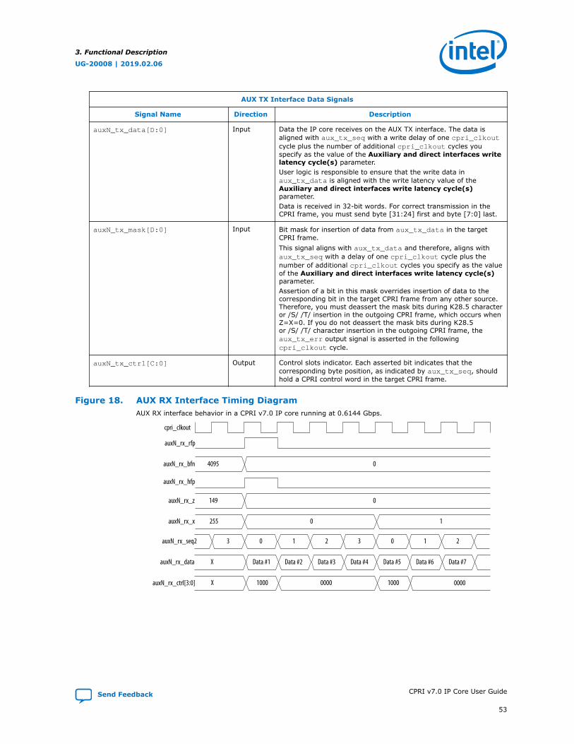
AUX TX Interface Data Signals
Signal Name Direction Description
auxN_tx_data[D:0] Input Data the IP core receives on the AUX TX interface. The data isaligned with aux_tx_seq with a write delay of one cpri_clkoutcycle plus the number of additional cpri_clkout cycles youspecify as the value of the Auxiliary and direct interfaces writelatency cycle(s) parameter.User logic is responsible to ensure that the write data inaux_tx_data is aligned with the write latency value of theAuxiliary and direct interfaces write latency cycle(s)parameter.Data is received in 32-bit words. For correct transmission in theCPRI frame, you must send byte [31:24] first and byte [7:0] last.
auxN_tx_mask[D:0] Input Bit mask for insertion of data from aux_tx_data in the targetCPRI frame.This signal aligns with aux_tx_data and therefore, aligns withaux_tx_seq with a delay of one cpri_clkout cycle plus thenumber of additional cpri_clkout cycles you specify as the valueof the Auxiliary and direct interfaces write latency cycle(s)parameter.Assertion of a bit in this mask overrides insertion of data to thecorresponding bit in the target CPRI frame from any other source.Therefore, you must deassert the mask bits during K28.5 characteror /S/ /T/ insertion in the outgoing CPRI frame, which occurs whenZ=X=0. If you do not deassert the mask bits during K28.5or /S/ /T/ character insertion in the outgoing CPRI frame, theaux_tx_err output signal is asserted in the followingcpri_clkout cycle.
auxN_tx_ctrl[C:0] Output Control slots indicator. Each asserted bit indicates that thecorresponding byte position, as indicated by aux_tx_seq, shouldhold a CPRI control word in the target CPRI frame.
Figure 18. AUX RX Interface Timing DiagramAUX RX interface behavior in a CPRI v7.0 IP core running at 0.6144 Gbps.
4095 0
0
3
255 1
149 0
2 0 1 2 3 0 1 2
X Data #1 Data #2 Data #3 Data #4 Data #5
cpri_clkout
auxN_rx_rfp
auxN_rx_bfn
auxN_rx_hfp
auxN_rx_z
auxN_rx_x
auxN_rx_seq
auxN_rx_data
auxN_rx_ctrl[3:0]
Data #6
0000 1000 0000
Data #7
X 1000
3. Functional Description
UG-20008 | 2019.02.06
Send Feedback CPRI v7.0 IP Core User Guide
53

Figure 19. CPRI REC Master Response to aux_tx_sync_rfp Resynchronization PulseAsserting aux_tx_sync_rfp resets the hyperframe and basic frame numbers in an REC master CPRI v7.0 IPcore. Shown for a CPRI v7.0 IP core running at 0.6144 Gbps.
21 22
216
3
215 1
98 0
2 0 1 0 1 2 3 0
cpri_clkout
auxN_tx_rfp
auxN_tx_bfn
auxN_tx_hfp
auxN_tx_hfn
auxN_tx_x
auxN_tx_seq
auxN_tx_sync_rfp
0
3. Functional Description
UG-20008 | 2019.02.06
CPRI v7.0 IP Core User Guide Send Feedback
54

Figure 20. AUX TX Interface Timing Diagram with One Auxiliary Latency CycleExpected behavior on the AUX TX interface of a CPRI v7.0 IP core running at 0.6144 Gbps. Illustrates the effectof setting the Auxiliary and direct interfaces write latency cycle(s) parameter to a a non-zero value.Shown for a CPRI v7.0 IP core with Auxiliary and direct interfaces write latency cycle(s) set to the valueof 1.
clock cycles write latency
4095 0
0
3
255 1
149 0
2 0 1 2 3 0 1 2
X Data #1 Data #2 Data #3 Data #4 Data #5
Data #5
X Mask #1 Mask #2 Mask #3 Mask #4 Mask #5
0 1 2 3 0 01 2 3
X Data #1 Data #2 Data #3 Data #4
cpri_clkout
auxN_tx_rfp
auxN_tx_bfn
auxN_tx_hfp
auxN_tx_hfn
auxN_tx_x
auxN_tx_seq
auxN_tx_data
auxN_tx_mask
Sequence Nnumberat actual CPRI frame
Actual frame data
Default one cpri_clkout cycledelay to write
Default delay + 1
Auxiliary latency cycle(s) == 1:
3. Functional Description
UG-20008 | 2019.02.06
Send Feedback CPRI v7.0 IP Core User Guide
55

Figure 21. AUX TX Interface Timing Diagram with Four Auxiliary Latency CyclesExpected behavior on the AUX TX interface of a CPRI v7.0 IP core running at 0.6144 Gbps. Illustrates the effectof setting the Auxiliary and direct interfaces write latency cycle(s) parameter to the value of four.
clock cycles write latency
4095 0
0
3
255 1
149 0
2 0 1 2 3 0 1 2
X Data #1 Data #2 Data #3 Data #4 Data #5
Data #5
X Mask #1 Mask #2 Mask #3 Mask #4 Mask #5
0 1 2 3 0 01 2 3
X Data #1 Data #2 Data #3 Data #4
cpri_clkout
auxN_tx_rfp
auxN_tx_bfn
auxN_tx_hfp
auxN_tx_hfn
auxN_tx_x
auxN_tx_seq
auxN_tx_data
auxN_tx_mask
Sequence Nnumberat actual CPRI frame
Actual frame data
Default one cpri_clkout cycledelay to write
Default delay + 4
Auxiliary latency cycle(s) == 1:
3. Functional Description
UG-20008 | 2019.02.06
CPRI v7.0 IP Core User Guide Send Feedback
56

Figure 22. AUX TX Timing Diagram with Error
Illustrates the behavior of the aux_tx_err signal on the AUX TX interface of a CPRI v7.0 IP core running at0.6144 Gbps. The aux_tx_ctrl signal shows that when aux_tx_seq has the value of zero, the first byte atthe corresponding position in the target CPRI frame is a control byte. The value of the Auxiliary and directinterfaces write latency cycle(s) parameter is zero. Therefore, the data on aux_tx_data is delayed by oneclock cycle from the value on aux_tx_seq. The data that appears on aux_tx_data when aux_tx_seq hasthe value of 1 is the data that targets position X.Y.Z.0 in the target CPRI frame.
The value of Mask #1 is presumably 0xFFXXXXXX, indicating that the incoming data on aux_tx_data isintended to overwrite this control byte in the target CPRI frame. Therefore, in the following cpri_clkoutcycle, the IP core asserts the aux_tx_err signal.
4095 0
0
3
255 1
149 0
2 0 1 2 3 0 1 2
X Data #1 Data #2 Data #3 Data #4 Data #5
cpri_clkout
auxN_tx_rfp
auxN_tx_bfn
auxN_tx_hfp
auxN_tx_hfn
auxN_tx_x
auxN_tx_seq
auxN_tx_data
auxN_tx_mask
Auxiliary latency cycle(s) == 0
Data #6
X Mask #1 Mask #2 Mask #3 Mask #4 Mask #5 Mask #6
0000
0000 0000
1000
1000
0000 1000 0000
auxN_tx_err[3:0]
auxN_tx_ctrl[3:0]
Related Information
• AUX Interface Synchronization on page 58Illustrates the relationship between the AUX synchronization signals.
• Auxiliary Latency Cycles on page 58The Auxiliary and direct interfaces write latency cycle(s) parameteraffects the relative timing of the data on the aux_tx_data and aux_tx_maskbusses. This section provides an explanation of the parameter's effect andpurpose.
3. Functional Description
UG-20008 | 2019.02.06
Send Feedback CPRI v7.0 IP Core User Guide
57

3.5.2. AUX Interface Synchronization
Figure 23. Relationship Between Synchronization Pulses and Numbers on the AUXInterfaceThe output synchronization signals are useful for custom user logic, including frame synchronization acrosshops in multi-hop configurations.
The output synchronization signals are derived from the CPRI frame synchronization state machine.
auxN_{rx,tx}_rfp
auxN_{rx,tx}_bfn
auxN_{rx,tx}_hfp
auxN_{rx,tx}_z
auxN_{rx,tx}_x
auxN_{rx,tx}_seq 0 1 ... NUM_SEQ - 1
2 ...
...210
255
149
10
n n + 1 n + 2
Hyperframe
Radio Frame (10 ms)
Basic Frame
Related Information
AUX Interface Signals on page 51Describes the AUX interface signals and provides AUX interface timing diagrams.
3.5.3. Auxiliary Latency Cycles
Intel provides configurable write latency on the AUX TX interface and other direct TXinterfaces to support user logic with sufficient advance notice of the position in theCPRI frame. The processing time that user logic requires after determining the currentposition in the CPRI frame is implementation specific, and the default write latency ofa single cpri_clkout cycle might not be adequate. Using the Auxiliary and directinterfaces write latency cycle(s) parameter, you can set the write latency to thenumber of clock cycles required for your system to process data before sending it onthe AUX TX interface or other direct TX interface.
3. Functional Description
UG-20008 | 2019.02.06
CPRI v7.0 IP Core User Guide Send Feedback
58

In the CPRI v7.0 parameter editor, you can specify a non-zero number of Auxiliaryand direct interfaces write latency cycle(s) to increase the write latency on theAUX TX interface and other direct TX interfaces to the CPRI v7.0 IP core.
The write latency is the number of cpri_clkout cycles from when the aux_tx_seqoutput signal has the value of n to when user logic must write data to the AUX TXinterface to target the corresponding position in the CPRI frame. For other directinterfaces, the IP core notifies user logic when it is ready for input and the user doesnot need to monitor the aux_tx_seq signal. However, the Auxiliary latencycycle(s) value does apply to all of the direct interfaces.
When Auxiliary and direct interfaces write latency cycle(s) has the default valueof zero, the write latency on the direct TX interfaces is one cpri_clkout cycle. WhenAuxiliary and direct interfaces write latency cycle(s) has the value of N, thewrite latency is (1+N) cpri_clkout cycles.
User logic is responsible to ensure that the data presented to the IP core on the AUXTX interface is presented at the correct write latency relative to the AUX TX interfacesynchronization signals.
Note: You cannot simply write to the AUX TX interface with a consistent write latency thatyou determine after configuring your IP core. If you do not specify the correct writelatency in the CPRI v7.0 parameter editor, the data you present on the AUX TXinterface cannot fill the correct position in the target CPRI frame. To ensure the writelatency offset is implemented correctly in the IP core, you must set the parameter.
Figure 24. AUX Interface Transmit Write LatencyIllustrates the transmit write latency on the AUX interface when Auxiliary and direct interfaces writelatency cycle(s) has the value of 0. If you specify a non-zero value for this parameter, the latency increasesfrom the default latency of one cpri_clkout cycle to 1 plus the number of cycles you specify.
In this example, the CPRI line bit rate is 6.144 Gbps, so that the control word is 10bytes. User logic masks the control word, so that the IP core does not receive thecontrol words from the AUX interface.
auxN_tx_seq[5:0]
internal tx_seq value[5:0]
CPRI Frame
210 3 3939 38
38
Ct rl Ct rl {Ctrl,feed}
0 1 2 3 393839
auxN_tx_mask[31:0]
auxN_tx_data[31:0]
0000ffff ffffffff
00000000 00000000 ffffffff ffffffff
0000feed abcdabcd
abcdabcd
00000000 00000000
1 cpri_clkout cycledefault write latency
3.5.4. Direct Interface CPRI Frame Data Format
The information on the AUX interface and all of the other direct interfaces except theL1 CSR interface, appears in the relevant data bus in 32-bit words. The CPRI v7.0 IPcore converts the contents of the incoming CPRI frame to a 32-bit format internally.
3. Functional Description
UG-20008 | 2019.02.06
Send Feedback CPRI v7.0 IP Core User Guide
59

Similarly, the IP core expects to receive data on the various direct interfaces in thisformat. The only exception is the L1 CSR interface, which transmits and receivesinformation in individual bits.
3. Functional Description
UG-20008 | 2019.02.06
CPRI v7.0 IP Core User Guide Send Feedback
60
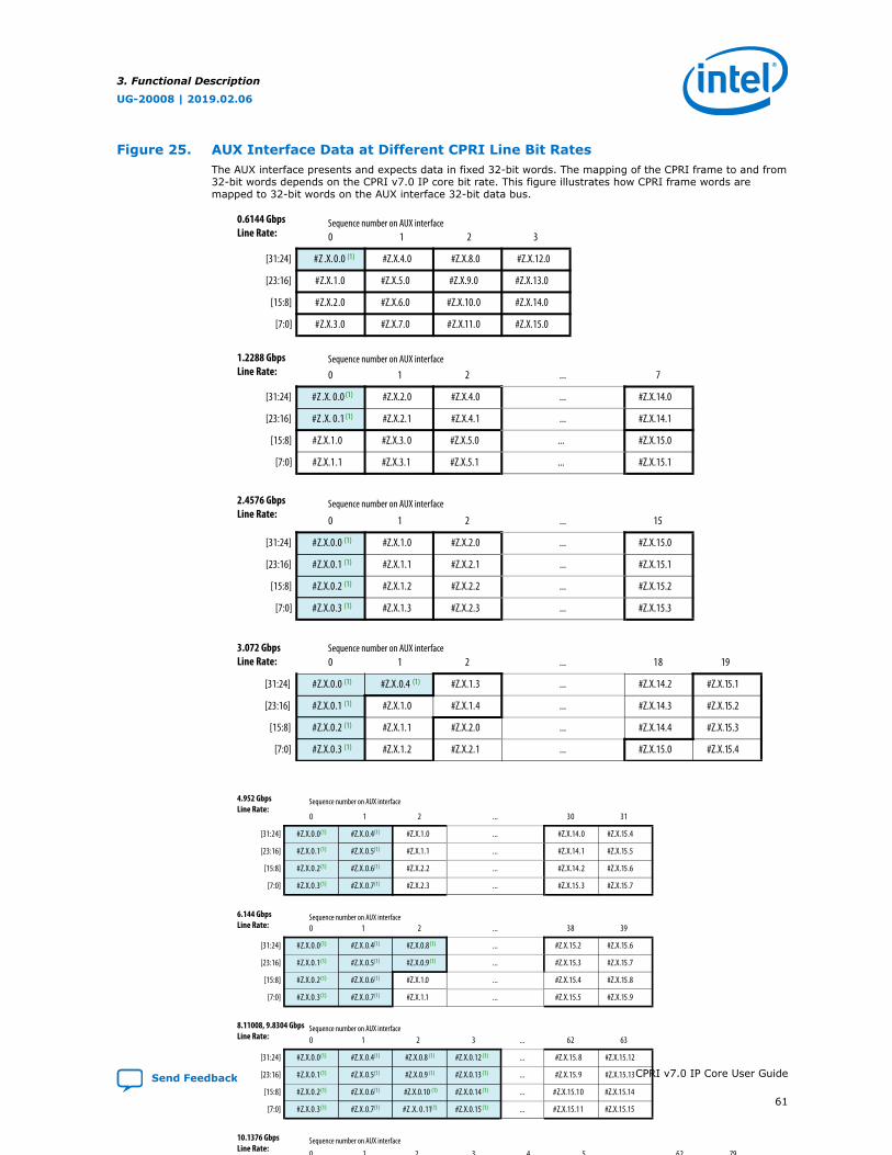
Figure 25. AUX Interface Data at Different CPRI Line Bit RatesThe AUX interface presents and expects data in fixed 32-bit words. The mapping of the CPRI frame to and from32-bit words depends on the CPRI v7.0 IP core bit rate. This figure illustrates how CPRI frame words aremapped to 32-bit words on the AUX interface 32-bit data bus.
0.6144 GbpsLine Rate:
1.2288 GbpsLine Rate:
2.4576 GbpsLine Rate:
3.072 GbpsLine Rate:
0 1 2 3
[31:24] #Z .X.0.0 (1) #Z.X.4.0 #Z.X.8.0 #Z.X.12.0
[23:16] #Z.X.1.0 #Z.X.5.0 #Z.X.9.0 #Z.X.13.0
[15:8] #Z.X.2.0 #Z.X.6.0 #Z.X.10.0 #Z.X.14.0
[7:0] #Z.X.3.0 #Z.X.7.0 #Z.X.11.0 #Z.X.15.0
0 1 2 ... 7
[31:24] #Z .X. 0.0 (1) #Z.X.2.0 #Z.X.4.0 ... #Z.X.14.0
[23:16] #Z .X. 0.1 (1) #Z.X.2.1 #Z.X.4.1 ... #Z.X.14.1
[15:8] #Z.X.1.0 #Z.X.3. 0 #Z.X.5.0 ... #Z.X.15.0
[7:0] #Z.X.1.1 #Z.X.3.1 #Z.X.5.1 ... #Z.X.15.1
0 1 2 ... 15
[31:24] #Z.X.0.0 (1) #Z.X.1.0 #Z.X.2.0 ... #Z.X.15.0
[23:16] #Z.X.0.1 (1) #Z.X.1.1 #Z.X.2.1 ... #Z.X.15.1
[15:8] #Z.X.0.2 (1) #Z.X.1.2 #Z.X.2.2 ... #Z.X.15.2
[7:0] #Z.X.0.3 (1) #Z.X.1.3 #Z.X.2.3 ... #Z.X.15.3
0 1 2 ... 18 19
[31:24] #Z.X.0.0 (1) #Z.X.0.4 (1) #Z.X.1.3 ... #Z.X.14.2 #Z.X.15.1
[23:16] #Z.X.0.1 (1) #Z.X.1.0 #Z.X.1.4 ... #Z.X.14.3 #Z.X.15.2
[15:8] #Z.X.0.2 (1) #Z.X.1.1 #Z.X.2.0 ... #Z.X.14.4 #Z.X.15.3
[7:0] #Z.X.0.3 (1) #Z.X.1.2 #Z.X.2.1 ... #Z.X.15.0 #Z.X.15.4
Sequence number on AUX interface
Sequence number on AUX interface
Sequence number on AUX interface
Sequence number on AUX interface
0 1 2 ... 30 31
[31:24] #Z.X.0.0(1) #Z.X.0.4(1) #Z.X.1.0 ... #Z.X.14.0 #Z.X.15.4
[23:16] #Z.X.0.1(1) #Z.X.0.5(1) #Z.X.1.1 ... #Z.X.14.1 #Z.X.15.5
[15:8] #Z.X.0.2(1) #Z.X.0.6(1) #Z.X.2.2 ... #Z.X.14.2 #Z.X.15.6
[7:0] #Z.X.0.3(1) #Z.X.0.7(1) #Z.X.2.3 ... #Z.X.15.3 #Z.X.15.7
0 1 2 ... 38 39
[31:24] #Z.X.0.0(1) #Z.X.0.4(1) #Z.X.0.8(1) ... #Z.X.15.2 #Z.X.15.6
[23:16] #Z.X.0.1(1) #Z.X.0.5(1) #Z.X.0.9(1) ... #Z.X.15.3 #Z.X.15.7
[15:8] #Z.X.0.2(1) #Z.X.0.6(1) #Z.X.1.0 ... #Z.X.15.4 #Z.X.15.8
[7:0] #Z.X.0.3(1) #Z.X.0.7(1) #Z.X.1.1 ... #Z.X.15.5 #Z.X.15.9
0 1 2 3 ... 62 63
[31:24] #Z.X.0.0(1) #Z.X.0.4(1) #Z.X.0.8 (1) #Z.X.0.12 (1) ... #Z.X.15.8 #Z.X.15.12
[23:16] #Z.X.0.1(1) #Z.X.0.5(1) #Z.X.0.9 (1) #Z.X.0.13 (1) ... #Z.X.15.9 #Z.X.15.13
[15:8] #Z.X.0.2(1) #Z.X.0.6(1) #Z.X.0.10 (1) #Z.X.0.14 (1) ... #Z.X.15.10 #Z.X.15.14
[7:0] #Z.X.0.3(1) #Z.X.0.7(1) #Z .X. 0.11(1) #Z.X.0.15 (1) ... #Z.X.15.11 #Z.X.15.15
0 1 2 3 62 79
[31:24] #Z.X.0.0(1) #Z.X.0.4(1) #Z.X.0.8 (1) #Z.X.0.12 (1) ...
[23:16] #Z.X.0.1(1) #Z.X.0.5(1) #Z.X.0.9 (1) #Z.X.0.13 (1) ...
[15:8] #Z.X.0.2(1) #Z.X.0.6(1) #Z.X.0.10 (1) #Z.X.0.14 (1) ...
[7:0] #Z.X.0.3(1) #Z.X.0.7(1) #Z .X. 0.11(1) #Z.X.0.15 (1) ...
#Z.X.0.16
#Z.X.0.17
#Z.X.0.18
#Z.X.0.19
#Z.X.1.0
#Z.X.1.1
#Z.X.1.2
#Z.X.1.3
4 5 ...
#Z.X.15.12
#Z.X.15.13
#Z.X.15.14
#Z.X.15.15
#Z.X.15.16
#Z.X.15.17
#Z.X.15.18
#Z.X.15.19
4.952 GbpsLine Rate:
Sequence number on AUX interface
6.144 GbpsLine Rate:
Sequence number on AUX interface
8.11008, 9.8304 GbpsLine Rate:
Sequence number on AUX interface
10.1376 GbpsLine Rate:
Sequence number on AUX interface
Note:(1) Light blue table cells indicate control word bytes. Yellow table cells indicate real-time vendor specific bytes. White table cells indicate data word bytes.
3. Functional Description
UG-20008 | 2019.02.06
Send Feedback CPRI v7.0 IP Core User Guide
61

The CPRI IP core passes the incoming AUX data through to the CPRI link unmodified.You must ensure that the incoming AUX data bits already include any CRC valuesexpected by the application at the other end of the CPRI link.
Figure 26. Data Sample Order on aux_tx_data and aux_rx_data BusesIllustrates how CPRI frame data is ordered in each 32-bit word.
31 24 23 16 15 8 7 0
I[3]
Q[3]
I[2]
Q[2]
I[1]
Q[1]
I[0]
Q[0]
I[7]
Q[7]
I[6]
Q[6]
I[5]
Q[5]
I[4]
Q[4]
I[11]
Q[11
]I[1
0]Q[
10]
I[9]
Q[9]
I[8]
Q[8]
I[15]
Q[15
]I[1
4]Q[
14]
I[13]
Q[13
]I[1
2]Q[
12]
3.6. Direct IQ Interface
If you turn on Enable direct IQ mapping interface in the CPRI v7.0 parametereditor, the direct IQ interface is available. This interface allows direct access to the I/Qdata time slots in the CPRI frame. You can connect this interface to any user-definedair standard I/Q mapping module.
This interface is Avalon-ST compliant with a read latency value of 1.
You can alter the transmit latency with the Auxiliary and direct interfaces writelatency cycle(s) parameter.
Table 23. Direct IQ Interface SignalsAll interface signals are clocked by the cpri_clkout clock. The Data path width parameter determines theinterface type and width, where N= 32 or 64, C= 3 or 7, and D= 31 or 63.
Direct IQ RX Interface
Signal Name Direction Description
iqN_rx_valid[C:0] Output Each asserted bit indicates the corresponding byte on the currentiq_rx_data bus is valid I/Q data.
iqN_rx_data[D:0] Output I/Q data received from the CPRI frame. The iq_rx_valid signalindicates which bytes are valid I/Q data bytes.
Direct IQ TX Interface
Signal Name Direction Description
iqN_tx_ready[C:0] Output Each asserted bit indicates the IP core is ready to read I/Q datafrom the corresponding byte of iq_tx_data on the next clockcycle.
iqN_tx_valid[C:0] Input Write valid for iq_tx_data. Assert bit [n] to indicate that thecorresponding byte on the current iq_tx_data bus is valid I/Qdata.
iqN_tx_data[D:0] Input I/Q data to be written to the CPRI frame. The IP core writes theindividual bytes of the current value on the iq_tx_data bus tothe CPRI frame based on the iq_tx_ready signal from theprevious cycle, and the iq_tx_valid signal in the current cycle.
3. Functional Description
UG-20008 | 2019.02.06
CPRI v7.0 IP Core User Guide Send Feedback
62

Figure 27. Direct IQ RX Interface Timing DiagramDirect IQ RX interface behavior in a CPRI v7.0 IP core running at 0.6144 Gbps.
The aux_rx_x and aux_rx_seq signals are not part of this interface and are available only if you turn on theAUX interface in your CPRI v7.0 IP core variation. However, their presence in the timing diagram explains thetiming of the iq_rx_valid output signal that you use to identify the clock cycles with valid I/Q data.
cpri_clkout
aux_rx_x[7:0]
aux_rx_seq[6:0]
iq_rx_valid[3:0]
2 3 4
2 3 0 1 2 3 0 1 2 3
1111 0111 1111 0111 1111
(IQ)(IQ) (IQ)(IQ)(IQ)(IQ) X(IQ)(IQ)(IQ) (IQ)(IQ)(IQ)(IQ) (IQ)(IQ)(IQ)(IQ) (IQ)(IQ)(IQ)(IQ) X(IQ)(IQ)(IQ) (IQ)(IQ)(IQ)(IQ) (IQ)(IQ)(IQ)(IQ) (IQ)(IQ)(IQ)(IQ)iq_rx_data[31:0]
Figure 28. Direct IQ TX Interface Timing DiagramExpected behavior on the direct IQ TX interface of a CPRI v7.0 IP core running at 0.6144 Gbps.
The aux_tx_x and aux_tx_seq signals are not part of this interface and are available only if you turn on theAUX interface in your CPRI v7.0 IP core variation. However, their presence in the timing diagram explains thetiming of the iq_tx_ready output signal that you use to identify the clock cycles when you can write I/Q datato the CPRI frame. Note that the write latency is two cpri_clkout clock cycles in this example.
cpri_clkout
aux_tx_x[7:0]
aux_tx_seq[6:0]
iq_tx_ready[3:0]
iq_tx_valid[3:0]
2 3 4
2 3 0 1 2 3 0 1 2 3
1111 0111 1111 0111 1111
1111 0111 1111 0111 1111
(IQ)(IQ) (IQ)(IQ)(IQ)(IQ) (IQ)(IQ)(IQ)(IQ) (IQ)(IQ)(IQ)(IQ) X(IQ)(IQ)(IQ) (IQ)(IQ)(IQ)(IQ) (IQ)(IQ)(IQ)(IQ) (IQ)(IQ)(IQ)(IQ) X(IQ)(IQ)(IQ) (IQ)(IQ)(IQ)(IQ)iq_tx_data[31:0]
Auxiliary latency cycle(s) == 1
Related Information
Avalon Interface SpecificationsFor more information about the Avalon-ST protocol, including timing diagrams,refer to the Avalon Streaming Interfaces chapter.
3.7. Ctrl_AxC Interface
If you turn on Enable direct ctrl_axc access interface in the CPRI v7.0 parametereditor, the Ctrl_AxC interface is available. This interface allows direct access to theCtrl_AxC subchannels in the CPRI frame, which are subchannels 4, 5, 6, and 7 in eachhyperframe.
This interface is Avalon-ST compliant with a read latency value of 1.
3. Functional Description
UG-20008 | 2019.02.06
Send Feedback CPRI v7.0 IP Core User Guide
63

You can alter the transmit latency with the Auxiliary and direct interfaces writelatency cycle(s) parameter.
Table 24. Ctrl_AxC Interface SignalsAll interface signals are clocked by the cpri_clkout clock. The Data path width parameter determines theinterface type and width, where N= 32 or 64, C= 3 or 7, and D= 31 or 63.
Ctrl_AxC RX Interface
Signal Name Direction Description
ctrlN_axc_rx_valid[C:0] Output Each asserted bit indicates the corresponding byte on the currentctrl_axc_rx_data bus is valid Ctrl_Axc data.
ctrlN_axc_rx_data[D:0] Output Ctrl_Axc data received from the CPRI frame. Thectrl_axc_rx_valid signal indicates which bytes are validCtrl_Axc data bytes.
Ctrl_AxC TX Interface
Signal Name Direction Description
ctrlN_axc_tx_ready[C:0] Output Each asserted bit indicates the IP core is ready to read Ctrl_Axcdata from the corresponding byte of ctrl_axc_tx_data on thenext clock cycle.
ctrlN_axc_tx_valid[C:0] Input Write valid for ctrl_axc_tx_data. Assert bit [n] to indicate thatthe corresponding byte on the current ctrl_axc_tx_data bus isvalid Ctrl_Axc data.
ctrl_axc_tx_data[D:0] Input Ctrl_Axc data to be written to the CPRI frame. The IP core writesthe individual bytes of the current value on thectrl_axc_tx_data bus to the CPRI frame based on thectrl_axc_tx_ready signal from the previous cycle, and thectrl_axc_tx_valid signal in the current cycle.
Figure 29. Ctrl_Axc RX Interface Timing DiagramCtrl_Axc RX interface behavior in a CPRI v7.0 IP core running at 0.6144 Gbps.
The aux_rx_x and aux_rx_seq signals are not part of this interface and are available only if you turn on theAUX interface in your CPRI v7.0 IP core variation. However, their presence in the timing diagram explains thetiming of the ctrl_axc_rx_valid output signal that you use to identify the clock cycles with valid Ctrl_Axcdata.
cpri_clkout
131 132 133 136 137
3 4 5 8 9
0000 1000 000000001000
X (D2)XXX XX(D1)XXX
aux_rx_x
aux_rx_x[5:0]
ctrl_axc_rx_valid[3:0]
ctrl_axc_rx_data[31:0]
3. Functional Description
UG-20008 | 2019.02.06
CPRI v7.0 IP Core User Guide Send Feedback
64

Figure 30. Ctrl_Axc TX Interface Timing DiagramExpected behavior on the Ctrl_Axc TX interface of a CPRI v7.0 IP core running at 0.6144 Gbps.
The aux_tx_x and aux_tx_seq signals are not part of this interface and are available only if you turn on theAUX interface in your CPRI v7.0 IP core variation. However, their presence in the timing diagram explains thetiming of the ctrl_axc_tx_ready output signal that you use to identify the clock cycles when you can writeCtrl_Axc data to the CPRI frame. Note that the write latency is two cpri_clkout clock cycles in this example.
cpri_clkout
131 132 133 136 137
3 4 5 8 9
0000 1000 000000001000
X 1000 XX1000
X (D2)XXX XX(D1)XXX
aux_tx_x
aux_tx_x[5:0]
ctrl_axc_tx_ready[3:0]
ctrl_axc_tx_valid[3:0]
ctrl_axc_tx_data[31:0]
Auxiliary latency cycle(s) == 1
Related Information
Avalon Interface SpecificationsFor more information about the Avalon-ST protocol, including timing diagrams,refer to the Avalon Streaming Interfaces chapter.
3.8. Direct Vendor Specific Access Interface
If you turn on Enable direct vendor specific access interface in the CPRI v7.0parameter editor, the direct vendor specific access interface is available. This interfaceallows direct access to the Vendor Specific subchannels in the CPRI hyperframe. TheVendor Specific information is present only in subchannels 16 through (P-1) of theCPRI hyperframe, where P is the Fast C&M pointer value. Check the vs_rx_validand vs_tx_ready signals to ensure you read and write this interface at the time thatcorresponds to the correct position in the CPRI frame. If you implement the AUXinterface, you can read the value on the aux_rx_x or aux_tx_x output signal toidentify the current position in the frame.
This interface is Avalon-ST compliant with a read latency value of 1.
You can alter the transmit latency with the Auxiliary and direct interfaces writelatency cycle(s) parameter.
Table 25. Direct Vendor Specific Access Interface Signals
All interface signals are clocked by the cpri_clkout clock. The Data path width parameter determines theinterface type and width, where N= 32 or 64, C= 3 or 7, and D= 31 or 63.
Direct Vendor Specific RX Interface
Signal Name Direction Description
vsN_rx_valid[C:0] Output Each asserted bit indicates the corresponding byte on the currentvs_rx_data bus is a valid vendor-specific byte.
vsN_rx_data[D:0] Output Vendor-specific word received from the CPRI frame. Thevs_rx_valid signal indicates which bytes are valid vendor-specific bytes.
3. Functional Description
UG-20008 | 2019.02.06
Send Feedback CPRI v7.0 IP Core User Guide
65

Direct Vendor Specific TX Interface
Signal Name Direction Description
vsN_tx_ready[C:0] Output Each asserted bit indicates the IP core is ready to receive avendor-specific byte from the corresponding byte of vs_tx_dataon the next clock cycle.
vsN_tx_valid[C:0] Input Write valid for vs_tx_data. Assert bit [n] of vs_tx_valid toindicate that byte [n] on the vs_tx_data bus holds a valid valuein the current clock cycle.
vsN_tx_data[D:0] Input Vendor-specific word to be written to the CPRI frame. The IP corewrites the individual bytes of the current value on thevs_tx_data bus to the CPRI frame based on the vs_tx_readysignal from the previous cycle, and the vs_tx_valid signal in thecurrent cycle.
Figure 31. Direct VS RX Timing DiagramDirect VS RX interface behavior in a CPRI v7.0 IP core running at 0.6144 Gbps.
The aux_rx_x signal is not part of this interface and is available only if you turn on the AUX interface in yourCPRI v7.0 IP core variation. However, its presence in the timing diagram explains the timing of thevs_rx_valid output signal that you use to identify the clock cycles with valid VS data.
The aux_rx_x[7:0] signal (labelled simply aux_rx_x) holds the eight-bit index of the basic frame in thehyperframe, from the perspective of the AUX interface. The subchannel index is the control word index modulo64, available in aux_rx_x[5:0] if you turn on the AUX interface in your CPRI IP core.
cpri_clkout
79 80 81 124 125
15 16 17 60 61
0000 1000 000000001000
X (D2)XXX XX(D1)XXX
aux_rx_x
aux_rx_x[5:0]
vs_rx_valid[3:0]
vs_rx_data[31:0]
Pointer-P = 60
3. Functional Description
UG-20008 | 2019.02.06
CPRI v7.0 IP Core User Guide Send Feedback
66
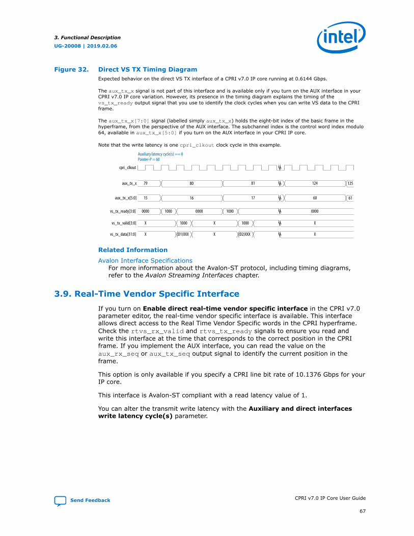
Figure 32. Direct VS TX Timing DiagramExpected behavior on the direct VS TX interface of a CPRI v7.0 IP core running at 0.6144 Gbps.
The aux_tx_x signal is not part of this interface and is available only if you turn on the AUX interface in yourCPRI v7.0 IP core variation. However, its presence in the timing diagram explains the timing of thevs_tx_ready output signal that you use to identify the clock cycles when you can write VS data to the CPRIframe.
The aux_tx_x[7:0] signal (labelled simply aux_tx_x) holds the eight-bit index of the basic frame in thehyperframe, from the perspective of the AUX interface. The subchannel index is the control word index modulo64, available in aux_tx_x[5:0] if you turn on the AUX interface in your CPRI IP core.
Note that the write latency is one cpri_clkout clock cycle in this example.
cpri_clkout
79 80 81 124 125
15 16 17 60 61
0000 1000 000000001000
X 1000 XX1000
X (D2)XXX XX(D1)XXX
aux_tx_x
aux_tx_x[5:0]
vs_tx_ready[3:0]
vs_tx_valid[3:0]
vs_tx_data[31:0]
Auxiliary latency cycle(s) == 0Pointer-P = 60
Related Information
Avalon Interface SpecificationsFor more information about the Avalon-ST protocol, including timing diagrams,refer to the Avalon Streaming Interfaces chapter.
3.9. Real-Time Vendor Specific Interface
If you turn on Enable direct real-time vendor specific interface in the CPRI v7.0parameter editor, the real-time vendor specific interface is available. This interfaceallows direct access to the Real Time Vendor Specific words in the CPRI hyperframe.Check the rtvs_rx_valid and rtvs_tx_ready signals to ensure you read andwrite this interface at the time that corresponds to the correct position in the CPRIframe. If you implement the AUX interface, you can read the value on theaux_rx_seq or aux_tx_seq output signal to identify the current position in theframe.
This option is only available if you specify a CPRI line bit rate of 10.1376 Gbps for yourIP core.
This interface is Avalon-ST compliant with a read latency value of 1.
You can alter the transmit write latency with the Auxiliary and direct interfaceswrite latency cycle(s) parameter.
3. Functional Description
UG-20008 | 2019.02.06
Send Feedback CPRI v7.0 IP Core User Guide
67
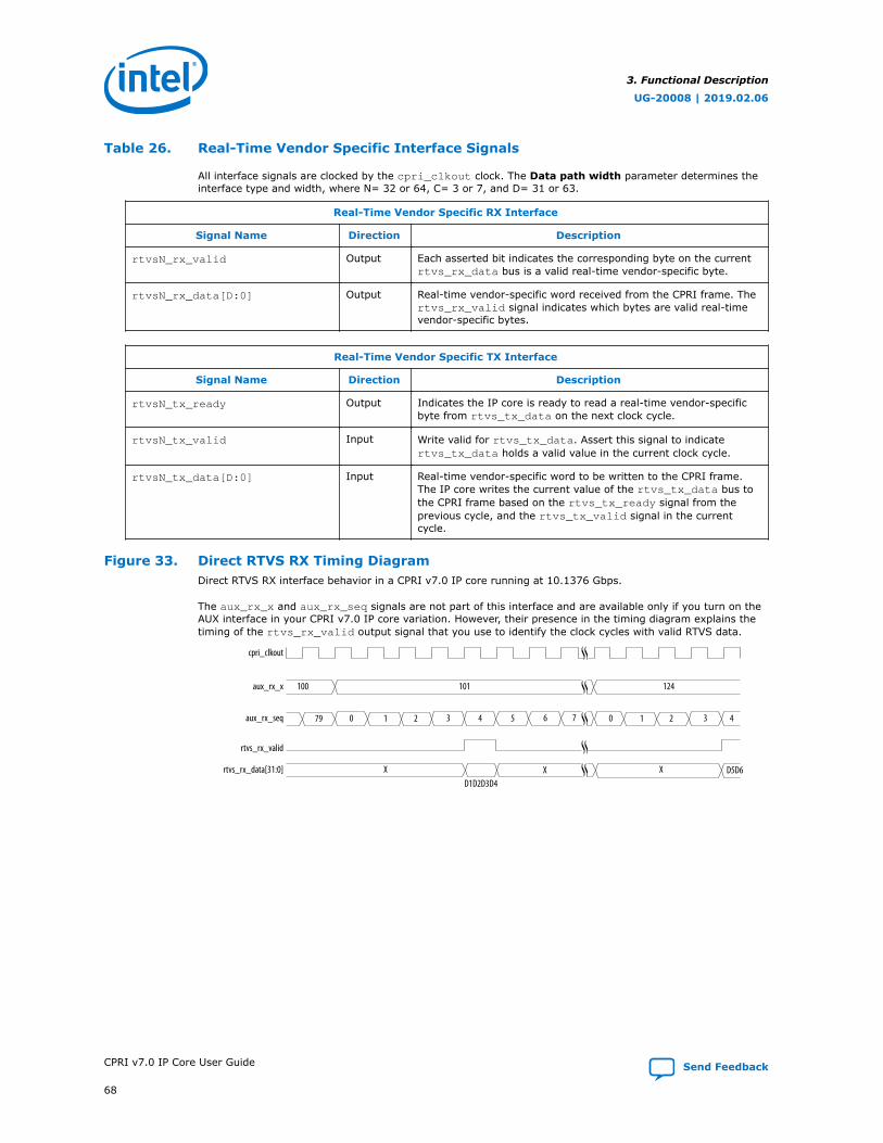
Table 26. Real-Time Vendor Specific Interface Signals
All interface signals are clocked by the cpri_clkout clock. The Data path width parameter determines theinterface type and width, where N= 32 or 64, C= 3 or 7, and D= 31 or 63.
Real-Time Vendor Specific RX Interface
Signal Name Direction Description
rtvsN_rx_valid Output Each asserted bit indicates the corresponding byte on the currentrtvs_rx_data bus is a valid real-time vendor-specific byte.
rtvsN_rx_data[D:0] Output Real-time vendor-specific word received from the CPRI frame. Thertvs_rx_valid signal indicates which bytes are valid real-timevendor-specific bytes.
Real-Time Vendor Specific TX Interface
Signal Name Direction Description
rtvsN_tx_ready Output Indicates the IP core is ready to read a real-time vendor-specificbyte from rtvs_tx_data on the next clock cycle.
rtvsN_tx_valid Input Write valid for rtvs_tx_data. Assert this signal to indicatertvs_tx_data holds a valid value in the current clock cycle.
rtvsN_tx_data[D:0] Input Real-time vendor-specific word to be written to the CPRI frame.The IP core writes the current value of the rtvs_tx_data bus tothe CPRI frame based on the rtvs_tx_ready signal from theprevious cycle, and the rtvs_tx_valid signal in the currentcycle.
Figure 33. Direct RTVS RX Timing DiagramDirect RTVS RX interface behavior in a CPRI v7.0 IP core running at 10.1376 Gbps.
The aux_rx_x and aux_rx_seq signals are not part of this interface and are available only if you turn on theAUX interface in your CPRI v7.0 IP core variation. However, their presence in the timing diagram explains thetiming of the rtvs_rx_valid output signal that you use to identify the clock cycles with valid RTVS data.
cpri_clkout
100 101 124
7 46
aux_rx_x
aux_rx_seq
rtvs_rx_valid
XD1D2D3D4
Xrtvs_rx_data[31:0]
54321079 3210
D5D6X
3. Functional Description
UG-20008 | 2019.02.06
CPRI v7.0 IP Core User Guide Send Feedback
68

Figure 34. Direct RTVS TX Timing DiagramExpected behavior on the direct RTVS TX interface of a CPRI v7.0 IP core running at 10.1376 Gbps.
The aux_tx_x and aux_tx_seq signals are not part of this interface and are available only if you turn on theAUX interface in your CPRI v7.0 IP core variation. However, their presence in the timing diagram explains thetiming of the rtvs_tx_ready output signal that you use to identify the clock cycles when you can write RTVSdata to the CPRI frame.
Note that the write latency is one cpri_clkout clock cycle in this example.
cpri_clkout
100 101 124
7 46
aux_tx_x
aux_tx_seq
rtvs_tx_ready
rtvs_tx_valid
XD1D2D3D4
Xrtvs_tx_data[31:0]
54321079 3210
Auxiliary latency cycle(s) == 0
Related Information
Avalon Interface SpecificationsFor more information about the Avalon-ST protocol, including timing diagrams,refer to the Avalon Streaming Interfaces chapter.
3.10. Direct HDLC Serial Interface
If you turn on Enable direct HDLC serial interface in the CPRI v7.0 parametereditor, the direct HDLC serial interface is available. This interface allows direct accessto the slow control and management data in the CPRI frame. You can connect thisinterface to a user-defined HDLC PCS and MAC.
This interface is Avalon-ST compliant with a read latency value of 1.
You can alter the transmit write latency with the Auxiliary and direct interfaceswrite latency cycle(s) parameter. However, you do not need to view theaux_tx_seq signal for correct alignment. You can monitor the hdlc_rx_valid andhdlc_tx_ready signals to discover the correct times to read and write data on thisinterface.
Table 27. Direct HDLC Serial Interface SignalsAll interface signals are clocked by the cpri_clkout clock.
Direct HDLC Serial RX Interface
Signal Name Direction Description
hdlc_rx_valid Output When asserted, indicates hdlc_rx_data holds a valid HDLC bit inthe current clock cycle.
hdlc_rx_data Output HDLC data stream received from the CPRI frame. Thehdlc_rx_valid signal indicates which bits are valid HDLC bytes.
3. Functional Description
UG-20008 | 2019.02.06
Send Feedback CPRI v7.0 IP Core User Guide
69

Direct HDLC Serial TX Interface
Signal Name Direction Description
hdlc_tx_ready Output When asserted, indicates the IP core is ready to receive HDLC datafrom hdlc_tx_data on the next clock cycle.
hdlc_tx_valid Input Write valid for hdlc_tx_data. Assert this signal to indicate thathdlc_tx_data holds a valid HDLC bit in the current clock cycle.
hdlc_tx_data Input HDLC data stream to be written to the CPRI frame directly. The IPcore writes the current value on hdlc_tx_data to the CPRI framebased on the hdlc_tx_ready signal from the previous cycle, andthe hdlc_tx_valid signal in the current cycle.
Figure 35. Direct HDLC Serial RX Timing DiagramHDLC Serial RX interface behavior in a CPRI v7.0 IP core running at 0.6144 Gbps.
cpri_clkout
hdlc_rx_valid
1 XX 0 1 0 1 0hdlc_rx_data
Figure 36. Direct HDLC Serial TX Timing DiagramExpected behavior on the HDLC Serial TX interface of a CPRI v7.0 IP core running at 0.6144 Gbps.
cpri_clkout
hdlc_tx_ready
hdlc_tx_valid
1 XX 0 1 0 1 0hdlc_tx_data
Related Information
Avalon Interface SpecificationsFor more information about the Avalon-ST protocol, including timing diagrams,refer to the Avalon Streaming Interfaces chapter.
3.11. Direct L1 Control and Status Interface
If you turn on Enable direct Z.130.0 alarm bits access interface in the CPRI v7.0parameter editor, the direct L1 control and status interface is available. This interfaceprovides direct access to the Z.130.0 alarm and reset signals (loss of frame (LOF),loss of signal (LOS), service access point (SAP) defect indication (SDI), remote alarmindication (RAI), and reset request or acknowledge) in the CPRI hyperframe.
If you connect the AUX interface of your RE slave IP core to a network switch or otherrouting layer rather than directly to the downstream RE master, or if you do not fullyconnect the AUX interface to the downstream RE master, you can use this Z.130.0access interface to streamline the transfer of reset requests and SDI alarms acrosshops.
This interface has higher transmit priority than access through the CPRI v7.0 IP coreregisters.This interface has the following types of signals:
3. Functional Description
UG-20008 | 2019.02.06
CPRI v7.0 IP Core User Guide Send Feedback
70

• _local_ signals are output signals from the IP core about the state of this IPcore, and also indicate the IP core asserts the relevant outgoing Z.130.0 bit in thenext CPRI hyperframe according to the transmit priority of this interface.
• _assert signals are input signals the application can use to request that the IPcore assert the relevant outgoing Z.130.0 bit in the next CPRI hyperframeaccording to the transmit priority of this interface. You can also connect thesesignals in an RE master to the corresponding _req output signals of the upstreamRE slave in a multi-hop configuration, to support efficient transfer of resetrequests and SDI alarms to the IP core.
• _remote signals are output signals from the IP core that indicate the IP corereceived a Z.130.0 byte on the CPRI link with the relevant bit asserted by theCPRI link partner.
• _req signals are also output signals from the IP core that indicate the IP corereceived a Z.130.0 byte on the CPRI link with the relevant bit asserted by theCPRI link partner. However, these signals are intended to be passed downstreamin a multi-hop configuration. If the IP core is an RE slave, and it connects to an REmaster through the Z.130.0 alarm and reset interface in a multi-hop configuration,you can connect the RE slave IP core _req output signal directly to thecorresponding _assert input signal on the downstream RE master for efficientcommunication of the reset request or SDI alarm.
Table 28. Direct L1 Control and Status Interface Signals
All interface signals are clocked by the cpri_clkout clock.
Signal Name Direction Description
z130_local_lof Output Indicates the IP core has detected a local loss of frame. In thiscase, the state_l1_synch output signal indicates the L1synchronization state machine is in state XACQ1 or XACQ2.In this case the IP core also asserts the local_lof bit in theFLSAR register at offset 0x2C.
z130_local_los Output Indicates the IP core has detected a local loss of signal. The IPcore asserts this flag if it detects excessive 8B/10B errors thattrigger the assertion of the optional L1 debug rx_lcv outputsignal or the xcvr_los output signal and the rx_los field of theL1_CONFIG register.In this case the IP core also asserts the local_los bit in theFLSAR register at offset 0x2C.
z130_sdi_assert Input Indicates that the master service access point (SAP) is notavailable. Possible causes for this situation are equipment error orthat the connected slave IP core is forwarding an SDI request itdetected to the current RE CPRI master IP core through a directconnection.
z130_local_rai Output Indicates that either the z130_local_lof or thez130_local_los signal is high; clears when both of those twosignals are low. Logical OR of two output signals z130_local_lofand z130_local_los.
z130_reset_assert Input Reset request from the application or from an RE slave to thecurrent RE CPRI master IP core through a direct connection.
z130_remote_lof Output Indicates LOF received in Z.130.0 control byte from remote CPRIlink partner.In this case the IP core also asserts the remote_lof bit in theFLSAR register at offset 0x2C.
continued...
3. Functional Description
UG-20008 | 2019.02.06
Send Feedback CPRI v7.0 IP Core User Guide
71

Signal Name Direction Description
z130_remote_los Output Indicates LOS received in Z.130.0 control byte from remote CPRIlink partner.In this case the IP core also asserts the remote_los bit in theFLSAR register at offset 0x2C.
z130_sdi_req Output Indicates remote SAP defect indication received in Z.130.0 controlbyte from remote CPRI link master. If the current CPRI IP core isan RE slave in a multi-hop configuration, you should connect thisoutput signal directly to the z130_sdi_assert input signal of thedownstream RE master.
z130_remote_rai Output Asserts when either z130_remote_lof or z130_remote_los isasserted, and clears when both z130_remote_lof andz130_remote_los have the value of 0.In this case the IP core also asserts the rai_detected bit in theFLSAR register at offset 0x2C.
z130_reset_req Output If the current IP core is a CPRI link slave, indicates the IP corereceived a reset request in the Z.130.0 control byte from theremote CPRI link master.If the current IP core is a CPRI link master, indicates the IP corereceived a reset acknowledgement in the Z.130.0 control byte fromthe remote CPRI link slave.
Figure 37. sdi_assert to sdi_req on Direct L1 Control and Status Interface
cpri_clkout
Master z130_sdi_assert
DL Frame Z.130.0[2] (Internal)
Slave z130_sdi_req
Assert for at Least One ClockCycle to Ensure at Least OneHyperframe Z.13.0[2] Asserted
NearestZ.130.0 Bit [2]
Next Z.130.0 Bit [2]Is Not Asserted
For Longer Slave sdi_req Assertion (More than One Hyperframe),Hold sdl_assert for More than One Hyperframe or Assert for One Clock Cycle 3 Clock Cycles before Z.130.0 (See AUX Status Signals) at Each Hyperframe
Assertion after Detecting the First Z.130.0[2] Assertion
Hold Assertion for OneHyperframe until theNext Z.130.0[2] Detection
3. Functional Description
UG-20008 | 2019.02.06
CPRI v7.0 IP Core User Guide Send Feedback
72
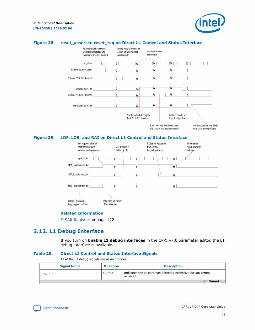
Figure 38. reset_assert to reset_req on Direct L1 Control and Status Interface
cpri_clkout
Master z130_reset_assert
DL Frame Z.130.0[0] (Internal)
Slave z130_reset_req
Assert for at Least One ClockCycle to Ensure at Least OneHyperframe Z.13.0[2] Asserted
Nearest Next 10 HyperframeZ.130.0 Bit [0] Is AssertedAutomatically
After Another NineHyperframes
Assertion after Detecting the Tenth Z.130.0[2] Assertion
Hold Assertion for at Least One Hyperframe
Slave Sends Next Five Hyperframesof Z.130.0[0] for Acknowledgement
Acknowledgement Signal Holdfor at Least One Hyperframe
UL Frame Z.130.0[0] (Internal)
Master z130_reset_req
Figure 39. LOF, LOS, and RAI on Direct L1 Control and Status Interface
cpri_clkout
z130_local/remote_lof
z130_local/remote_los
z130_local/remote_rai
LOF Happens after RXState Machine Lost Comma Synchronization
May or May NotFollow Up LOS
RX State Is Recoveringfrom Comma Resynchronization
remote_lof/los/raiOnly Happens to Slave
RAI Asserts wheneverLOF or LOS Asserts
HyperframeSynchronizationAchieved
Related Information
FLSAR Register on page 122
3.12. L1 Debug Interface
If you turn on Enable L1 debug interfaces in the CPRI v7.0 parameter editor, the L1debug interface is available.
Table 29. Direct L1 Control and Status Interface SignalsAll of the L1 debug signals are asynchronous.
Signal Name Direction Description
rx_lcv Output Indicates the IP core has detected excessive 8B10B errorsreceived.
continued...
3. Functional Description
UG-20008 | 2019.02.06
Send Feedback CPRI v7.0 IP Core User Guide
73
Signal Name Direction Description
The IP core asserts this signal when it detects more than 15 bits oferror.
rx_freq_alarm Output Indicates the CPRI receive clock (receiver CDR recovered clock)and the main IP core clock (cpri_clkout) have a PPM difference.The IP core asserts this alarm each time it detects a mismatch.
3.13. Media Independent Interface (MII) to External Ethernet Block
The media independent interface (MII) allows the CPRI v7.0 IP core to communicatedirectly with an external Ethernet MAC block. If you set the value of the EthernetPCS interface parameter in the CPRI v7.0 parameter editor to MII, your IP coreincludes this interface.
The MII supports the bandwidth described in the CPRI v7.0 Specification in Table 12,Achievable Ethernet bit rates.
Table 30. MII Signals
These signals are available if you set the value of the Ethernet PCS interface parameter in the CPRI v7.0parameter editor to MII. You can connect a user-defined Ethernet MAC to this interface.
The interface is fully compliant to the IEEE 802.3 100BASE-X 100Mbps MII specification. An Ethernet PCS blockin the CPRI v7.0 IP core ensures the interface bandwidth matches the current CPRI line bit rate and accessesdata at the correct CPRI frame positions according to the Z.194.0 pointer value.
You must monitor the MII FIFO status signals and ensure you do not overflow or underflow the FIFO.
The interface signals are clocked by the mii_rxclk or mii_txclk clock.
RX MII Signals
Signal Name Direction Description
mii_rxclk Input Clocks the MII receiver interface. You must drive this clock at thefrequency of 25 MHz to achieve the 100 Mbps bandwidth requiredfor this interface.
mii_rxreset_n Input Resets the MII receiver interface and FIFO read logic. This resetsignal is active low.
mii_rxdv Output Ethernet receive data valid. Indicates the presence of valid data orinitial K nibble on mii_rxd[3:0].
mii_rxer Output Ethernet receive error. Indicates an error in the current nibble ofmii_rxd. This signal is de-asserted at reset, and remains de-asserted while the CPRI v7.0 IP core is resetting and until linkinitialization completes.
mii_rxd[3:0] Output Ethernet receive nibble data. Data bus for data from the CPRI v7.0IP core to the external Ethernet block. All bits are de-assertedduring reset, and all bits are asserted after reset until the CPRIv7.0 IP core achieves frame synchronization.
3. Functional Description
UG-20008 | 2019.02.06
CPRI v7.0 IP Core User Guide Send Feedback
74

TX MII Signals
Signal Name Direction Description
mii_txclk Input Clocks the MII transmitter interface. You must drive this clock atthe frequency of 25 MHz to achieve the 100 Mbps bandwidthrequired for this interface.
mii_txreset_n Input Resets the MII transmitter interface and FIFO write logic. Thissignal is active low.
mii_txen Input Valid signal from the external Ethernet block, indicating thepresence of valid data on mii_txd[3:0]. The external Ethernetblock must also assert this signal two cycles before initial validdata, while the IP core inserts /J/ and /K/ nibbles in the datastream to form the start-of-packet symbol.
mii_txer Input Ethernet transmit coding error. When this signal is asserted, theCPRI v7.0 IP core inserts an Ethernet HALT symbol in the data itpasses to the CPRI link.
mii_txd[3:0] Input Ethernet transmit nibble data. The data transmitted from theexternal Ethernet block to the CPRI v7.0 IP core, for transmissionon the CPRI link. This input bus is synchronous to the rising edgeof the mii_txclk clock.
MII Status Signals
Signal Name Direction Description
mii_tx_fifo_status[3:0] Output Ethernet Tx PCS FIFO fill level status. The individual bits have thefollowing meanings:• Bit [3]: Empty• Bit [2]: Almost empty• Bit [1]: Full• Bit [0]: Almost full
mii_rx_fifo_status[3:0] Output Ethernet Rx PCS FIFO fill level status. The individual bits have thefollowing meanings:• Bit [3]: Empty• Bit [2]: Almost empty• Bit [1]: Full• Bit [0]: Almost full
Figure 40. RX MII Timing Diagram
mii_rxclk
mii_rxdv
mii_rxd
mii_rxer
D1 D2 /F/ D4 D5 D6 D7 XX
Error ReceivedDiscard Partof Payload
4’b0101
3. Functional Description
UG-20008 | 2019.02.06
Send Feedback CPRI v7.0 IP Core User Guide
75

Figure 41. TX MII Timing Diagram
mii_txclk
mii_txen
mii_txd
mii_txer
Encoded Frame
D1 D2 D3 D4 D5 D6 D7 XX
/J/ /K/ /D1/ /D2/ /F/ /D4/ /D5/ X/I/ /D6/ /D7/ /T/ /R/
Error InjectionDiscard Partof Payload
Related Information
CPRI v7.0 IP Core L2 Interface on page 107
3.14. Gigabit Media Independent Interface (GMII) to ExternalEthernet Block
The gigabit media independent interface (GMII) allows the CPRI v7.0 IP core tocommunicate directly with an external Ethernet MAC block. If you set the value of theEthernet PCS interface parameter in the CPRI v7.0 parameter editor to GMII, yourIP core includes this interface.
The GMII supports the bandwidth described in the CPRI v7.0 Specification in Table 12,Achievable Ethernet bit rates.
Table 31. GMII Signals
These signals are available if you set the value of the Ethernet PCS interface parameter in the CPRI v7.0parameter editor to GMII. You can connect a user-defined Ethernet MAC to this interface.
The interface is fully compliant to the IEEE 802.3 1000BASE-X 1Gbps MII specification. An Ethernet PCS blockin the CPRI v7.0 IP core ensures the interface bandwidth matches the current CPRI line bit rate and accessesdata at the correct CPRI frame positions according to the Z.194.0 pointer value.
You must monitor the GMII FIFO status signals and ensure you do not overflow or underflow the FIFO.
The interface signals are clocked by the gmii_rxclk or gmii_txclk clock.
RX GMII Signals
Signal Name Direction Description
gmii_rxclk Input Clocks the GMII receiver interface. You must drive this clock at thefrequency of 125 MHz.
gmii_rxreset_n Input Resets the GMII receiver interface and FIFO read logic. This resetsignal is active low.
continued...
3. Functional Description
UG-20008 | 2019.02.06
CPRI v7.0 IP Core User Guide Send Feedback
76

RX GMII Signals
Signal Name Direction Description
gmii_rxdv Output Ethernet receive data valid. Indicates the presence of valid data orinitial start-of-packet control character on gmii_rxd[7:0].
gmii_rxer Output Ethernet receive error. Indicates an error on gmii_rxd. When thissignal is asserted, the value on gmii_rxd[7:0] is 0x0E.
gmii_rxd[7:0] Output Ethernet receive data. Data bus for data from the CPRI v7.0 IPcore to the external Ethernet block. All bits are de-asserted duringreset, and all bits are asserted after reset until the CPRI v7.0 IPcore achieves frame synchronization.
TX GMII Signals
Signal Name Direction Description
gmii_txclk Input Clocks the GMII transmitter interface. You must drive this clock atthe frequency of 125 MHz.
gmii_txreset_n Input Resets the GMII transmitter interface and FIFO write logic. Thissignal is active low.
gmii_txen Input Valid signal from the external Ethernet block, indicating thepresence of valid data on gmii_txd[7:0]. This signal must beasserted two cycles before data is actually valid. This advancenotice provides time for the CPRI v7.0 GMII transmitter block toinsert an S character in the data stream to form the start-of-packetsymbol.Deasserting this signal triggers the IP core to insert T and Rcharacters in the data stream to form the end-of-packet symbol.
gmii_txer Input Ethernet transmit coding error. When this signal is asserted, theCPRI v7.0 IP core inserts an Ethernet Error Propagation symbol /V/in the data it passes to the CPRI link.
gmii_txd[7:0] Input Ethernet transmit data. The data transmitted from the externalEthernet block to the CPRI v7.0 IP core, for transmission on theCPRI link. This input bus is synchronous to the rising edge of thegmii_txclk clock.
MII Status Signals
Signal Name Direction Description
gmii_txfifo_status[3:0] Output Ethernet Tx PCS FIFO fill level status. The individual bits have thefollowing meanings:• Bit [3]: Empty• Bit [2]: Almost empty• Bit [1]: Full• Bit [0]: Almost full
gmii_rxfifo_status[3:0] Output Ethernet Rx PCS FIFO fill level status. The individual bits have thefollowing meanings:• Bit [3]: Empty• Bit [2]: Almost empty• Bit [1]: Full• Bit [0]: Almost full
3. Functional Description
UG-20008 | 2019.02.06
Send Feedback CPRI v7.0 IP Core User Guide
77
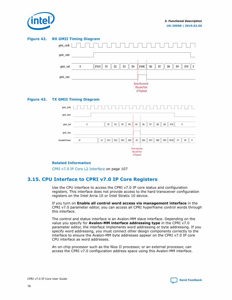
Figure 42. RX GMII Timing Diagram
gmii_rxclk
gmii_rxdv
gmii_rxd
gmii_rxer
D1 D2 D3 D4 8’h0E D6 D7 D8 D9 XD10X
Error ReceivedDiscard Partof Payload
8’h55
Figure 43. TX GMII Timing Diagram
/T/
D10
gmii_txclk
gmii_txen
gmii_txd
gmii_txer
Encoded Frame
D1 D2 D3 D4 D5 D6 D7X
/S/ /D1/ /D2/ /D3/ /D4/ /V//I/ /D6/ /D7/ /D8/ /D9/ X/D10/ /R/
XD8 D9
Error InjectionDiscard Partof Payload
Related Information
CPRI v7.0 IP Core L2 Interface on page 107
3.15. CPU Interface to CPRI v7.0 IP Core Registers
Use the CPU interface to access the CPRI v7.0 IP core status and configurationregisters. This interface does not provide access to the hard transceiver configurationregisters on the Intel Arria 10 or Intel Stratix 10 device.
If you turn on Enable all control word access via management interface in theCPRI v7.0 parameter editor, you can access all CPRI hyperframe control words throughthis interface.
The control and status interface is an Avalon-MM slave interface. Depending on thevalue you specify for Avalon-MM interface addressing type in the CPRI v7.0parameter editor, the interface implements word addressing or byte addressing. If youspecify word addressing, you must connect other design components correctly to theinterface to ensure the Avalon-MM byte addresses appear on the CPRI v7.0 IP coreCPU interface as word addresses.
An on-chip processor such as the Nios II processor, or an external processor, canaccess the CPRI v7.0 configuration address space using this Avalon-MM interface.
3. Functional Description
UG-20008 | 2019.02.06
CPRI v7.0 IP Core User Guide Send Feedback
78

Related Information
Avalon Interface SpecificationsFor more information about the Avalon-MM protocol, including timing diagrams,refer to the Avalon Memory-Mapped Interfaces chapter.
3.15.1. CPU Interface Signals
Table 32. CPRI v7.0 IP Core CPU Interface SignalsThe CPRI v7.0 IP core CPU interface has the following features:
• Avalon-MM slave interface compliant.
• Provides support for single cycle read and write operations: you can read or write a single register in asingle access operation.
• Supports a single cpu_clk clock cycle read latency and a zero cpu_clk clock cycle write latency for mostregisters.
Signal Name Direction Description
cpu_clk Input Clocks the signals on the CPRI v7.0 CPU interface. Supports anyfrequency that the device fabric supports.
cpu_reset_n Input Active low reset signal. Resets the CPRI v7.0 CPU interface and all ofthe registers to which it provides access.You should hold this signal asserted for one full cpu_clk cycle toensure it is captured by the IP core.
cpu_address[15:0] Input Address for reads and writes. All CPRI v7.0 control and statusregisters are 32 bits wide. By default, this address is a word address(addresses a 4-byte (32-bit) word), not a byte address. However, ifyou set Avalon-MM interface addressing type to Byte in theCPRI v7.0 parameter editor, this address is a byte address.
cpu_byteenable[3:0] Input Data-byte enable signal
cpu_read Input You must assert this signal to request a read transfer
cpu_write Input You must assert this signal to request a write transfer
cpu_writedata[31:0] Input Write data
cpu_readdata[31:0] Output Read data
cpu_waitrequest Output Indicates that the control and status interface is busy executing anoperation. When the IP core deasserts this signal, the operation iscomplete and the read data is valid.
cpu_irq Output Interrupt request. All interrupts that you enable in the relevantregister fields, assert this interrupt signal when they are triggered.You must check the relevant register fields to determine the cause orcauses of the interrupt assertion.
Figure 44. Read Transaction on CPU Interface
cpu_waitrequest
cpu_writecpu_address[15:0]
cpu_byteenable[3:0]cpu_writedata[31:0]
cpu_readcpu_readdata[31:0]
0000h
0h00000000h
00000000h
0008h
Fh
00000002h
3. Functional Description
UG-20008 | 2019.02.06
Send Feedback CPRI v7.0 IP Core User Guide
79

Figure 45. Write Transaction on CPU Interface
cpu_waitrequest
cpu_writecpu_address[15:0]
cpu_byteenable[3:0]cpu_writedata[31:0]
cpu_readcpu_readdata[31:0]
0008h
fh00000007h
00000000h
000Ch
0h
Related Information
Avalon Interface SpecificationsFor more information about the Avalon-MM protocol, refer to the Avalon Memory-Mapped Interfaces chapter.
3.15.2. Accessing the Hyperframe Control Words
When you turn on Enable all control word access via management interface inthe CPRI v7.0 parameter editor, you can access the 256 control words in a hyperframethrough the CPRI v7.0 IP core CPU interface. The CTRL_INDEX register and theRX_CTRL register support your application in reading the incoming control words, andthe L1_CONFIG register, CTRL_INDEX register, and TX_CTRL register support theapplication in writing to outgoing control words.
Register support provides you access to the full control word. Alternatively, in timing-critical applications, you can access the full control words through the CPRI v7.0 IPcore AUX interface or other dedicated direct interfaces.
Note: Intel recommends that you use the CPU interface to access the hyperframe controlwords only in applications that are not timing-critical.
3. Functional Description
UG-20008 | 2019.02.06
CPRI v7.0 IP Core User Guide Send Feedback
80

3.15.2.1. Specifying the Control Word
Figure 46. Subchannels in a HyperframeIllustrates how the 256 control words in the hyperframe are organized as 64 subchannels of four control wordseach. The figure illustrates why the index X of a control word is Ns + 64 + Xs, where Ns is the subchannelindex and Xs is the index of the control word within the subchannel.
Xs == 0 1 2 3
Ns == 0 0: K28.5 Synchronization and Timing
1 1: HDLC link 65: HDLC 129: HDLC 193: HDLC
2 2: L1 In-band 66: L1 in-band 130: L1 in-band 194: P (20 = 0x14)
3 3: Reserved 67: Reserved
4 4: Ctrl_AxC ... ... ...
...
7 7: Ctrl_AxC 71: Ctrl_AxC 135: Ctrl_AxC 199: Ctrl_AxC
...
14 14: Reserved
15 15: Reserved 79: Reserved 143: Reserved 207: Reserved
16 Vendor-specific
...
19
20Pointer P --->
20: Ethernet
...
62 62 126 190 254
63 63 127 191 255
The rx_ctrl_x and tx_ctrl_x fields of the CTRL_INDEX register hold the X valueof the control word you want to access through the control and status interface.
3.15.2.2. Specifying the Position in the Control Word
You can access 32 bits in a single register access. Depending on the CPRI line bit rate,a control word may have multiple 32-bit sections. Therefore, in addition to specifyingthe control word location in the CPRI frame, you must also specify a 32-bit alignedposition in the control word.
3. Functional Description
UG-20008 | 2019.02.06
Send Feedback CPRI v7.0 IP Core User Guide
81

Table 33. Control Word Byte Positions in RX_CTRL and TX_CTRL RegistersIn this table, each control word nibble is indicated with 0xF. The presence of 0xF or 0x0 indicates whether thenibble within the register is populated with a valid control word nibble.
CPRIBit
Rate(Gbps)
Register Access Sequence Number ({rx,tx}_ctrl_seq)
0(first
access)
1(2nd
access)
2(3rd
access)
34th
access)
4(5th
access)
5(6th
access)
6(7th
access)
7(8th
access)
8(9th
access)
9(10th
access)
10(11th
access)
11(12th
access)
0.6144 FF000000
0 0 0 0 0 0 0 0 0 0 0
1.2288 FFFF0000
0 0 0 0 0 0 0 0 0 0 0
2.4576 FFFFFFFF
0 0 0 0 0 0 0 0 0 0 0
3.072 FFFFFFFF
FF000000
0 0 0 0 0 0 0 0 0 0
4.9152 FFFFFFFF
FFFFFFFF
0 0 0 0 0 0 0 0 0
6.144 FFFFFFFF
FFFFFFFF
FFFF0000
0 0 0 0 0 0 0 0 0
8.11008,
9.8034
FFFFFFFF
FFFFFFFF
FFFFFFFF
FFFFFFFF
0 0 0 0 0 0 0 0
10.1376
FFFFFFFF
FFFFFFFF
FFFFFFFF
FFFFFFFF
FF000000
0 0 0 0 0 0 0
12.16512
FFFFFFFF
FFFFFFFF
FFFFFFFF
FFFFFFFF
FFFFFFFF
FFFFFFFF
0 0 0 0 0 0
24.33024
FFFFFFFF
FFFFFFFF
FFFFFFFF
FFFFFFFF
FFFFFFFF
FFFFFFFF
FFFFFFFF
FFFFFFFF
FFFFFFFF
FFFFFFFF
FFFFFFFF
FFFFFFFF
However, the table does not clarify which control word byte occupies which position inthe register. The following examples indicate the correspondence between registerbytes and control word bytes:
• At the CPRI line bit rate of 0.6144 Gbps, when you access hyperframe controlword X, the 8-bit control word from hyperframe position #Z.X.0 is in bits [31:24]of the register.
• At the CPRI line bit rate of 1.2288 Gbps, the byte from position #Z.X.0.0 is in bits[31:24] of the register and the byte from position #Z.X.0.1 is in bits [23:16] ofthe register.
• At the CPRI line bit rate of 3.072 Gbps, you must access the register twice toretrieve or write the full control word. In the first access operation, you access the32 bits of the control word in positions #Z.X.0.0 (in register bits [31:24]),#Z.X.0.1 (in register bits [23:16]), #Z.X.0.2 (in register bits [15:8]), and#Z.X.0.3 (in register bits [7:0]). In the second access operation, you access theeight bits of the control word in position #Z.X.0.4 in bits [31:24] of the register.
3.15.2.3. Retrieving the Hyperframe Control Words
A control receive table contains one entry for each of the 256 control words in thecurrent hyperframe. To read a control word, your application must write the controlword number X to the rx_ctrl_x field of the CTRL_INDEX register and then read thelast received #Z.X control word from the RX_CTRL register. Because the register can
3. Functional Description
UG-20008 | 2019.02.06
CPRI v7.0 IP Core User Guide Send Feedback
82

hold only 32 bits at a time, depending on the CPRI line bit rate, reading the full controlword may require multiple register accesses. Increment the value in therx_ctrl_seq field of the CTRL_INDEX register from zero to four to access the fullcontrol word when the CPRI line bit rate is 10.1376 Gbps, or from zero to two whenthe CPRI line bit rate is 6.144 Gbps, for example.
Example 1. Control Word Retrieval Example
To retrieve the vendor-specific portion of a control word in the most recent receivedhyperframe, perform the following steps:
1. Identify the indices for the vendor-specific portion of the transmit control table,using the formula X = Ns + 64 + Xs.
In the example, Ns = 16 and Xs = 0, 1, 2, and 3. Therefore, the indices to be readare 16, 80, 144, and 208.
2. For each value X in 16, 80, 144, and 208, perform the following steps:
a. Write the value X to the rx_ctrl_x field of the CTRL_INDEX register.
b. Reset the rx_ctrl_seq field of the CTRL_INDEX register to the value ofzero.
c. In the following cpu_clk cycle, read the first 32-bit section of the controlword from the RX_CTRL register.
d. If the CPRI line bit rate is greater than 2.4576 Gbps, increment therx_ctrl_seq field of the CTRL_INDEX register to the value of 1 and in thefollowing cpu_clk cycle, read the second 32-bit section of the #Z.X controlword from the RX_CTRL register.
e. If the CPRI line bit rate is greater than 4.9152 Gbps, increment therx_ctrl_seq field of the CTRL_INDEX register to the value of 2 and in thefollowing cpu_clk cycle, read the third 32-bit section of the #Z.X controlword from the RX_CTRL register.
f. If the CPRI line bit rate is greater than 6.144 Gbps, increment therx_ctrl_seq field of the CTRL_INDEX register to the value of 3 and in thefollowing cpu_clk cycle, read the fourth 32-bit section of the #Z.X controlword from the RX_CTRL register.
g. If the CPRI line bit rate is 10.1376 Gbps, increment the rx_ctrl_seq field ofthe CTRL_INDEX register to the value of 4 and in the following cpu_clkcycle, read the fifth 32-bit section of the #Z.X control word (the real-timevendor specific bytes) from the RX_CTRL register.
3.15.2.4. Writing the Hyperframe Control Words
A control transmit table contains one entry for each of the 256 control words in thecurrent hyperframe. Each control transmit table entry contains a control word and anenable bit. As the frame is created, if a control word entry is enabled, and the globaltx_ctrl_insert_en bit in the L1_CONFIG register is set, the IP core writes theappropriate control transmit table entry to the CPRI frame's control word.
You write to a control transmit table entry through the TX_CTRL register. This registeraccess method requires that you write the control word in 32-bit sections. Use thetx_ctrl_seq field of the CTRL_INDEX register to specify the 32-bit section you arecurrently writing to the TX_CTRL register.
3. Functional Description
UG-20008 | 2019.02.06
Send Feedback CPRI v7.0 IP Core User Guide
83
To write a control word in the control transmit table, perform the following steps:
1. Write the control word number X to the tx_ctrl_x field of the CTRL_INDEXregister.
2. Reset the tx_ctrl_seq field of the CTRL_INDEX register to the value of zero.
3. Write the first 32-bit section of the next intended #Z.X control word to theTX_CTRL register.
4. If the CPRI line bit rate is greater than 2.4576 Gbps, increment the tx_ctrl_seqfield of the CTRL_INDEX register to the value of 1 and write the second 32-bitsection of the next intended #Z.X control word to the TX_CTRL register.
5. If the CPRI line bit rate is greater than 4.9152 Gbps, increment the tx_ctrl_seqfield of the CTRL_INDEX register to the value of 2 and write the third 32-bitsection of the next intended #Z.X control word to the TX_CTRL register.
6. If the CPRI line bit rate is greater than 6.144 Gbps, increment the tx_ctrl_seqfield of the CTRL_INDEX register to the value of 3 and write the fourth 32-bitsection of the next intended #Z.X control word to the TX_CTRL register.
7. If the CPRI line bit rate is 10.1376 Gbps, increment the tx_ctrl_seq field of theCTRL_INDEX register to the value of 4 and write the fifth 32-bit section of thenext intended #Z.X control word (the real-time vendor specific bytes) to theTX_CTRL register.
8. Set the tx_ctrl_insert bit of the CTRL_INDEX register to the value of 1.
9. After you update the control transmit table, set the tx_ctrl_insert_en bit ofthe L1_CONFIG register to enable the CPRI v7.0 IP core to write the values fromthe control transmit table to the control words in the outgoing CPRI frame.
The tx_control_insert bit of the CTRL_INDEX register enables or disables thetransmission of the corresponding control transmit table entry in the CPRI frame. Thetx_ctrl_insert_en bit of the L1_CONFIG register is the master enable: when it isset, the CPRI v7.0 IP core writes all table entries with the tx_ctrl_insert bit setinto the CPRI frame.
Example 2. Control Word Transmission Example
To write the vendor-specific portion of the control word in a transmitted hyperframe,perform the following steps:
1. Identify the indices for the vendor-specific portion of the transmit control table,using the formula X = Ns + 64 + Xs.
In the example, Ns = 16 and Xs = 0, 1, 2, and 3. Therefore, the indices to be readare 16, 80, 144, and 208.
2. For each value X in 16, 80, 144, and 208, perform the sequence of steps listedabove.
After you update the control transmit table with the control bytes, to insert thedata in the next outgoing CPRI frame, make sure that you setthetx_ctrl_insert_en bit of the L1_CONFIG register to the value of 1 asspecified in the instructions.
3. Functional Description
UG-20008 | 2019.02.06
CPRI v7.0 IP Core User Guide Send Feedback
84
3.16. Auto-Rate Negotiation
If you turn on Enable line bit rate auto-negotiation in the CPRI v7.0 parametereditor, the auto-rate negotiation control and status interface is available. The CPRIv7.0 IP core provides support for dynamically changing the CPRI line bit rate, butrequires that you implement user logic to control the auto-rate negotiation process.You control the process through the auto-rate negotiation control and status interfaceor the BIT_RATE_CONFIG register at offset 0x0C.
Table 34. Auto-Rate Negotiation Control and Status Interface Signals
All interface signals are clocked by the cpri_clkout clock.
Signal Name Direction Description
nego_bitrate_in[5:0] Input CPRI line bit rate to be used in next attempt to achieve framesynchronization, encoded according to the following valid values:• 6'b000001: 0.6144 Gbps• 6'b000010: 1.2288 Gbps• 6'b000100: 2.4576 Gbps• 6'b000101: 3.0720 Gbps• 6'b001000: 4.9150 Gbps• 6'b001010: 6.1440 Gbps• 6'b010110: 8.11008 Gbps• 6'b010000: 9.8304 Gbps• 6'b010100: 10.1376 Gbps• 6b'011000: 12.16512 Gbps• 6'b110000 : 24.33024 GbpsThis signal has higher priority than the bit_rate field in theBIT_RATE_CONFIG register at offset 0x0C. When this signal hasthe value of 5'b00000, the CPRI v7.0 IP core responds to theregister field.
nego_bitrate_out[4:0] Output Reflects the current actual CPRI line bit rate.
Related Information
BIT_RATE_CONFIG Register on page 118
3.17. Extended Delay Measurement
The CPRI v7.0 IP core employs an additional mechanism to measure the delay throughthe IP core FIFOs to your desired precision. Separate dedicated clocks support thismeasurement for the RX and TX internal buffers in all variations and for the hardFIFOs present only in Intel Stratix 10 variations.
Related Information
• TX_EX_DELAY Register on page 126
• RX_EX_DELAY Register on page 127
• Extended Delay Measurement Interface on page 88
3. Functional Description
UG-20008 | 2019.02.06
Send Feedback CPRI v7.0 IP Core User Guide
85

3.17.1. Extended Delay Measurement for Soft Internal Buffers
The CPRI v7.0 IP core uses a dedicated clock, ex_delay_clk, to measure the delaythrough the RX and TX internal buffers to your desired precision. The extended delayprocess is identical for the two directions of flow through the IP core; theTX_EX_DELAY and RX_EX_DELAY registers hold the same information for the twodirections.
The tx_msrm_period field of the TX_EX_DELAY register contains the value N, suchthat N clock periods of the ex_delay_clk clock are equal to some whole number Mof cpri_clkout periods. For example, N may be a multiple of M, or the M/Nfrequency ratio may be slightly greater than 1, such as 64/63 or 128/127. Theapplication layer specifies N to ensure the accuracy your application requires. Theaccuracy of the Tx buffer delay measurement is N/least_common_multiple(N,M)cpri_clkout periods.
Similarly, the rx_msrm_period field of the RX_EX_DELAY register contains the valueN, such that N clock periods of the ex_delay_clk clock are equal to some wholenumber M of cpri_clkout periods.
If your application does not require this precision, drive the ex_delay_clk input portwith the cpri_clkout signal. In this case, the M/N ratio is 1 because the frequenciesare the same.
The tx_buf_delay field of the TX_DELAY register indicates the number of 32-bitwords currently in the Tx buffer. After you program the tx_msrm_period field of theTX_EX_DELAY register with the value of N, the tx_ex_delay field of theTX_EX_DELAY register holds the current measured delay through the Tx buffer. Theunit of measurement is cpri_clkout periods. The tx_ex_delay_valid fieldindicates that a new measurement has been written to the tx_ex_delay field sincethe previous register read. The following sections explain how you set and use theseregister values to derive the extended Tx delay measurement information.
M/N Ratio Selection
As your selected M/N ratio approaches 1, the accuracy provided by the extended delaymeasurement increases.
Table 35. Resolution as a Function of M/N Ratio at 3.072 Gbps
M N cpri_clkout Period ex_delay_clk Period Resolution
128 127 13.02 ns (1/76.80 MHz) 13.12 ns ±100 ps
64 63 13.22 ns ±200 ps
1 4 3.25 ns ±3.25 ns
Example 3. Extended Delay Measurement Calculation Example
This section walks you through an example that shows you how to calculate thefrequency at which to run ex_delay_clk, and how to program and use the registersto determine the delay through the CPRI Receive Buffer.
For example, assume your CPRI v7.0 IP core runs at CPRI line bit rate 3.072 Gbps. Inthis case, the cpri_clkout frequency is 76.80, so a cpri_clkout cycle is 1/76.80MHz.
3. Functional Description
UG-20008 | 2019.02.06
CPRI v7.0 IP Core User Guide Send Feedback
86
If your accuracy resolution requirements are satisfied by an M/N ratio of 128/127,perform the following steps:
1. Program the value N=127 in the rx_msrm_period field of the RX_EX_DELAYregister at offset 0x54.
2. Perform the following calculation to determine the ex_delay_clk frequency thatsupports your desired accuracy resolution:
ex_delay_clk period = (M/N) cpri_clkout period = (128/127)(1/(76.80MHz)= 13.123356 ns.
Based on this calculation, the frequency of ex_delay_clk is 1/(13.123356 ns)
The following steps assume that you run ex_delay_clk at this frequency.
3. Read the value of the RX_EX_DELAY register at offset 0x54.
If the rx_ex_delay_valid field of the register is set to 1, the value in therx_ex_delay field has been updated, and you can use it in the followingcalculations. For this example, assume the value read from the rx_ex_delayfield is 0x107D, which is decimal 4221.
4. Perform the following calculation to determine the delay through the Rx buffer:
Delay through Rx buffer = (rx_ex_delay x cpri_clkout period) / N = (4221 x13.02083 ns) / 127 = 432.7632 ns.
This delay comprises (432.7632ns / 13 .02083 ns) = 33.236 cpri_clkout clockcycles.
These numbers provide you the result for this particular example. For illustration, thepreceding calculation shows the result in nanoseconds. You can derive the result incpri_clkout clock cycles by dividing the preceding result by the cpri_clkoutclock period. Alternatively, you can calculate the number of cpri_clkout clock cycles ofdelay through the Rx buffer directly, as rx_msrm_period/N.
3.17.2. Extended Delay Measurement for Intel Stratix 10 Hard FIFOs
The CPRI v7.0 IP core uses a dedicated clock, latency_sclk, to measure the delaythrough the RX and TX Intel Stratix 10 device hard FIFOs that are configured in theCPRI v7.0 IP core.
The delay calculation process is identical for the two directions of flow through the IPcore; the XCVR_TX_FIFO_DELAY and XCVR_RX_FIFO_DELAY registers hold the sameinformation for the two directions.
To measure the current Tx delay through the hard FIFOs:
• Check the tx_pcs_fifo_delay_valid and tx_core_fifo_delay_validfields of the XCVR_TX_FIFO_DELAY register at offset 0x84 to ensure the delaycount values are updated.
• Add the delay count values in the tx_pcs_fifo_delay andtx_core_fifo_delay fields of the XCVR_TX_FIFO_DELAY register at offset0x84.
• Multiply the result by the clock period of the latency_sclk.
• Divide this result by 128.
3. Functional Description
UG-20008 | 2019.02.06
Send Feedback CPRI v7.0 IP Core User Guide
87

To measure the current Rx delay through the hard FIFOs:
• Check the rx_pcs_fifo_delay_valid and rx_core_fifo_delay_validfields of the XCVR_RX_FIFO_DELAY register at offset 0x88 to ensure the delaycount values are updated.
• Add the delay count values in the rx_pcs_fifo_delay andrx_core_fifo_delay fields of the XCVR_RX_FIFO_DELAY register at offset0x88.
• Multiply the result by the clock period of the latency_sclk.
• Divide this result by 128.
Figure 47. Additional Delay Through Stratix 10 Hard FIFOs
PCS
Transceiver
CPRI v7.0 IP Core
Extended DelayM
easurement
FIFOPCS FIFO Core FIFO
PCS FIFO Core FIFO
AIB
AIB
FIFO
3.17.3. Extended Delay Measurement Interface
Table 36. Extended Delay Measurement Interface Signals
Signal Name Direction Description
ex_delay_clk Input Clock for extended delay measurement.
ex_delay_reset_n Input Resets the extended delay measurement block. This signal is active low.This reset signal is associated with the ex_delay_clk clock.
latency_sclk Input Clock for extended delay measurement of Intel Stratix 10 hard FIFOs.You can (but need not) drive this clock at the same frequency asex_delay_clk.
latency_sreset_n Input Resets the extended delay measurement soft logic for the Intel Stratix10 hard FIFOs. This signal is active low.This reset signal is associated with the latency_sclk clock.
3.18. Deterministic Latency and Delay Measurement and Calibration
The CPRI v7.0 IP core complies with CPRI v7.0 Specification requirements R-19, R-20,R-20A, R-21, and R-21A.
3.18.1. Delay Measurement and Calibration Features
The CPRI v7.0 Specification measurement and delay requirements support systemconfiguration and correct synchronization.
3. Functional Description
UG-20008 | 2019.02.06
CPRI v7.0 IP Core User Guide Send Feedback
88

The CPRI v7.0 IP core provides the following support for accurate delay measurement:
• Provides current Rx delay measurement values in the RX_DELAY andRX_EX_DELAY registers.
• Provides current Tx delay calibration values in the XCVR_BITSLIP register.
• Provides current round-trip delay measurement value in the ROUND_TRIP_DELAYregister.
• Supports user control over delay measurement accuracy in the TX_EX_DELAY andRX_EX_DELAY registers.
• If you turn on Enable round-trip delay calibration in the CPRI v7.0 parametereditor, supports round-trip delay calibration.
• If you turn on Enable single-trip delay calibration in the CPRI v7.0 parametereditor, supports single-trip delay calibration.
3.18.2. Delay Requirements
CPRI v7.0 Specification requirements R-17, R-18, and R-18A address jitter andfrequency accuracy in the RE core clock for radio transmission. The relevant clocksynchronization is performed using an external clean-up PLL that is not included in theCPRI v7.0 IP core.
CPR v7.0 Specification requirement R-20A addresses the maximum allowed delay inswitching between receiving and transmitting on the radio interface. The radiointerface is implemented outside the IP core based on raw data presented on the AUXinterface or other direct interfaces. Because the IP core provides duplexcommunication on these interfaces, no delay calculation is required.
Requirement R-19 specifies that the link delay accuracy for the downlink between thesynchronization master SAP and the synchronization slave SAP, excluding the cablelength, be within ±8.138 ns. Requirements R-20 and R-21 extrapolate thisrequirement to single-hop round-trip delay accuracy. R-20 requires that the accuracyof the round-trip delay, excluding cables, be within ±16.276 ns, and R-21 requiresthat the round-trip cable delay measurement accuracy be within the same range.Requirement R-21A extrapolates this requirement further, to multihop round-trip delayaccuracy. In calculating these delays, Intel assumes that the downlink and uplink cabledelays have the same duration.
Figure 48. Single-Hop CPRI v7.0 IP Core Configuration Delay Measurement ReferencePointsThe round-trip cable delay is the sum of the T12 and T34 delays. The two delays are assumed to have thesame duration.
RE SlaveREC Master
T12
round_trip_delay
optical link
aux_rx_rfp aux_tx_rfp
aux_rx_rfpaux_tx_sync_rfp
T_RX_8/10G_L1
T_TX_8/10G_L1
T_RX_8/10G_L1
T_TX_8/10G_L1
SAP
T14
T34
Transceiverand SFP
Transceiverand SFP
R4
R1
Toffset
SAP
R2
R3
T_S_
Rx_T
x
3. Functional Description
UG-20008 | 2019.02.06
Send Feedback CPRI v7.0 IP Core User Guide
89
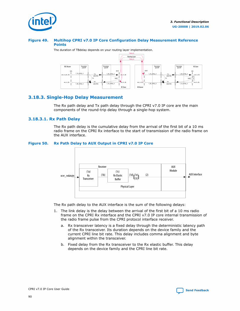
Figure 49. Multihop CPRI v7.0 IP Core Configuration Delay Measurement ReferencePointsThe duration of TBdelay depends on your routing layer implementation.
RE Slave
REC Master
T12optical link
optical link optical linkaux_rx_rfp aux_tx_rfp
aux_rx_rfpaux_tx_sync_rfp
TBdelay DL
SAPs
T_RX_8/10G_L1
T_TX_8/10G_L1
T14
T34
Transceiverand SFP
Transceiverand SFP
R4
R1
AUX IF
R2
R3
RE Slave
RE Master
T12optical link
aux_rx_rfp aux_tx_rfp
aux_rx_rfp
AUX IF
T14
T34
Transceiverand SFP
Transceiverand SFP
R4
R1
Toffset
SAPs
R2
R3
Routing LayerTBdelay UL
Toffset
T_TX_8/10G_L1
T_RX_8/10G_L1
T_TX_8/10G_L1
T_RX_8/10G_L1
T_RX_8/10G_L1
T_TX_8/10G_L1
T_S_
Rx_T
x
3.18.3. Single-Hop Delay Measurement
The Rx path delay and Tx path delay through the CPRI v7.0 IP core are the maincomponents of the round-trip delay through a single-hop system.
3.18.3.1. Rx Path Delay
The Rx path delay is the cumulative delay from the arrival of the first bit of a 10 msradio frame on the CPRI Rx interface to the start of transmission of the radio frame onthe AUX interface.
Figure 50. Rx Path Delay to AUX Output in CPRI v7.0 IP Core
AUX InterfaceRxTransceiver
Receiver
xcvr_rxdatain
Physical Layer
AUXModule
Rx ElasticBuffer
(1a) (1c)(1b) (2)(1d) (1e)
(1f)
The Rx path delay to the AUX interface is the sum of the following delays:
1. The link delay is the delay between the arrival of the first bit of a 10 ms radioframe on the CPRI Rx interface and the CPRI v7.0 IP core internal transmission ofthe radio frame pulse from the CPRI protocol interface receiver.
a. Rx transceiver latency is a fixed delay through the deterministic latency pathof the Rx transceiver. Its duration depends on the device family and thecurrent CPRI line bit rate. This delay includes comma alignment and bytealignment within the transceiver.
b. Fixed delay from the Rx transceiver to the Rx elastic buffer. This delaydepends on the device family and the CPRI line bit rate.
3. Functional Description
UG-20008 | 2019.02.06
CPRI v7.0 IP Core User Guide Send Feedback
90

Note: In IP core variations that target an Intel Stratix 10 device, you mustalso add the delay through the Stratix 10 hard FIFOs in the Rx path.
c. Delay through the clock synchronization FIFO, as well as the phase differencebetween the recovered receive clock and the core clock cpri_clkout. The"Extended Delay Measurement" section shows how to calculate the delay inthe CPRI v7.0 IP core Rx elastic buffer, which includes the phase differencedelay.
d. Byte alignment delay that can occur as data is shifted out of the receiver. Thisvariable delay appears in the rx_byte_delay field of the RX_DELAY register.When the value in rx_byte_delay is non-zero, a byte alignment delay of onecpri_clkout cycle occurs in the Rx path.
e. Variable delay introduced by the optional single-trip delay calibration featurein CPRI link slave IP cores.
f. Variable delay introduced by the optional round-trip delay calibration featurein CPRI link master IP cores.
2. Delay from the CPRI low-level receiver block to the AUX interface. This delaydepends on the device family and the CPRI line bit rate.
Related Information
RX_DELAY Register on page 126
3.18.3.2. Tx Path Delay
The Tx path delay is the cumulative delay from the arrival of the first bit of a 10 msradio frame on the CPRI AUX interface (or other direct interface) to the start oftransmission of this data on the CPRI link.
Figure 51. Tx Path Delay from AUX Interface to CPRI Link in CPRI v7.0 IP Core
TransmitterTransceiver
Transmitter
xcvr_txdataout
Physical Layer
AUXModule
(1)(5)
(4) (3) (2) AUX Interface
3. Functional Description
UG-20008 | 2019.02.06
Send Feedback CPRI v7.0 IP Core User Guide
91

The Tx path delay from the AUX interface to the CPRI link is the sum of the followingdelays:
1. Fixed delay from the AUX interface though the CPRI low-level transmitter to the Txelastic buffer. This delay depends on the device family and the current CPRI linebit rate.
2. Variable delay through the Tx elastic buffer, as well as the phase differencebetween the core clock cpri_clkout and the transceiver tx_clkout clock. The"Extended Delay Measurement" section shows how to calculate the delay in theCPRI v7.0 IP core Tx elastic buffer, which includes the phase difference delay.
3. Variable Tx bitslip delay in CPRI RE slaves. Refer to "Tx Bitslip Delay."
4. Fixed delay from the Tx elastic buffer to the transceiver. This delay depends on thedevice family and the CPRI line bit rate.
Note: In IP core variations that target an Intel Stratix 10 device, you must alsoadd the delay through the Stratix 10 hard FIFOs in the Tx path. Refer to"Extended Delay Measurement for Intel Stratix 10 Hard FIFOs" section.
5. Link delay through the transceiver.
Related Information
TX_DELAY Register on page 125
3.18.3.3. Round-Trip Delay
You can read the ROUND_TRIP_DELAY register or calculate the round-trip delay fromthe delay components (Rx path delay, Tx path delay,cable delay, and Rx-to-Txswitching latency). The round_trip_delay field of the ROUND_TRIP_DELAY registerin an REC master records the total round-trip delay from the start of the internaltransmit radio frame in the REC to the start of the internal receive radio frame in theREC, that is, from SAP to SAP, in CPRI REC and RE masters.
CPRI v7.0 Specification requirements R-20 and R-21 address the round-trip delay.Requirement R-20 addresses the measurement without including the cable delay, andrequirement R-21 is the requirement for the cable delay. Both requirements state thatthe variation must be no more than ±16.276 ns.
To monitor the round-trip delay, you must check periodically to confirm that thevariation in measurements over time is small enough that the requirements are met.
Note: The round trip delay is the sum of the Tx path delays through the REC master and theRE slave, the Rx path delays through the REC master and the RE slave, the cabledelay, and the Tx-to-Rx switching delay, sometimes referred to as the loopback delay.The Tx-to-Rx switching delay is labeled T_S_Rx_Tx in the figure. The Tx-to-Rxswitching delay depends on the loopback path and the device.
Related Information
ROUND_TRIP_DELAY Register on page 127
3.18.4. Multi-Hop Delay Measurement
In a multi-hop system, you must combine the delays between and through thedifferent CPRI masters and CPRI RE slaves to determine the round-trip delay.
3. Functional Description
UG-20008 | 2019.02.06
CPRI v7.0 IP Core User Guide Send Feedback
92

To determine the round-trip delay of a full multi-hop system, you must add togetherthe values in the ROUND_TRIP_DELAY registers of the REC and RE masters in thesystem, plus the delays through the external routers, and subtract the loopback delayfrom all the hops except the final hop.
Round-trip delay = Σi round_trip_delay (hop i) + Σj (TBdelayUL + TBdelayDL)(j) – ΣjT_S_Rx_Tx(j)
where the REC and RE masters in the configuration are labeled i = 0, 1, ...,n and therouting layers in the configuration, and their uplink and downlink delays, are labeled j= 0, 1, ...(n-1).
As the equation shows, you must omit the loopback delay from the single-hopcalculation for all but the final pair of CPRI link partners. The loopback delay is onlyrelevant at the turnaround point of the full multi-hop path.
3.18.5. Delay Calibration Features
The CPRI v7.0 IP core provides multiple calibration features to support compliancewith the CPRI v7.0 Specification.
• If you turn on Enable single-trip delay calibration in the CPRI v7.0 parametereditor, supports single-trip delay calibration using the DELAY_CAL_STD_CTRL1,DELAY_CAL_STD_CTRL2, DELAY_CAL_STD_CTRL3, DELAY_CAL_STD_CTRL3,DELAY_CAL_STD_CTRL4, DELAY_CAL_STD_CTRL5, andDELAY_CAL_STD_STATUS registers. You can connect the IOPLL and DPCU blocksthat Intel provides with the CPRI v7.0 IP core to ensure correct calibration results.
• If you turn on Enable round-trip delay calibration in the CPRI v7.0 parametereditor, supports round-trip delay calibration using the DELAY_CAL_RTD register.
• In all supported device families, increases the consistency of the round-trip delayusing the XCVR_BITSLIP register.
3.18.5.1. Single-Trip Delay Calibration
The CPRI v7.0 IP core provides an optional mechanism to support calibrating the totaldelay through a CPRI master and slave on the downlink in a single hop.
If you turn on Enable single-trip delay calibration in the CPRI v7.0 parametereditor, the CPRI v7.0 IP core and IOPLL and dynamic phase control unit (DPCU) blockswork together to adjust the delay through the RE slave Rx path in response toinformation about the delay through the REC or RE master Tx path.
3. Functional Description
UG-20008 | 2019.02.06
Send Feedback CPRI v7.0 IP Core User Guide
93

Figure 52. Downlink Slave Delay Adjustment for Single-Trip Delay Calibration
Master TX FIFO Slave RX FIFO
CPRILink
SAPm SAPs
Before Calibration
After Calibration
0s
0sAddedDelay
DesiredLatency
Before Calibration
After Calibration
0s
0sReduced
Delay
DesiredLatency
Example 1: Example 2:
The feature introduces the new delay to maintain a single-trip delay measurement asclose as possible to the desired single-trip delay you provide to the CPRI v7.0 IP core.The application can also provide Tx path delay information that is appropriate forother use scenarios. For example, you might want to adjust the latency to thesynchronization SAP to compensate for the IQ mapper requirements in your system.Refer to the Altera wiki Latency Formula and Calculation Example page.
Figure 53. Single-Trip Delay Does Not Affect Link Delay
Master TX FIFO Slave RX FIFO
HSSI
SAPm SAPs
Before Calibration
After Calibration 1
After Calibration 2
Fixed Round-Trip Delay
Downlink Delay is Guaranteed Fixed
to User Input Value
Slave TX FIFO Master RX FIFO
HSSI
SAPm
The cal_cycle_delay and cal_step_delay fields of the DELAY_CAL_STD_CTRL2register in the CPRI link slave hold the anticipated delay that you program. Thecal_current_delay field of the DELAY_CAL_STD_STATUS register in the CPRI linkslave holds the total actual variable delay measurement in the single trip from thesynchronization SAP in the CPRI link master to the synchronization SAP in the currentCPRI link slave. You can manually specify a consistency check whenever you want, oryou can specify that the IP core should run a consistency check once everyhyperframe.
If you turn on single-trip delay calibration by setting the cal_en bit in theDELAY_CAL_STD_CTRL1 register, the single-trip calibration feature is active. The userprograms the cal_cycle_delay and cal_step_delay fields with the number of
3. Functional Description
UG-20008 | 2019.02.06
CPRI v7.0 IP Core User Guide Send Feedback
94
whole and fractional cpri_clkout cycles of single-trip variable delay that the systemrequires. After each consistency check, the CPRI v7.0 slave IP core adjusts the Rxdelay to compensate for mismatches between the programmed, required single-tripdelay and the actual single-trip variable delay recorded in the cal_current_delayregister field. The delay adjustment mechanism is dynamic phase shifting of thecpri_coreclk.
The slave IP core requires the master IP core measured Tx delay information tocalculate the cal_current_delay value. The master IP core sends this informationto its downlink slave by one of two possible mechanisms. You program the master IPcore DELAY_CAL_STD4 register to specify whether the master sends this informationin the incoming hyperframe (and at which location in the hyperframe) or the systemwrites it in the dedicated slave IP core DELAY_CAL_STD_CTRL5 register. You programthe slave IP core DELAY_CAL_STD3 register to specify whether the slave receives thisinformation in the incoming hyperframe (and at which location in the hyperframe) orthe system writes it in the dedicated slave DELAY_CAL_STD_CTRL5 register. If bothCPRI master and slave are CPRI v7.0 IP cores, and the register values in the CPRI linkmaster and slave do not match, the single-trip delay calibration does not functioncorrectly. If the CPRI master is not a CPRI v7.0 IP core, the CPRI slave must receivethe correct information in the programmed register or hyperframe location.
Related Information
Intel FPGA Wiki CPRI IP v6 Latency Formula and Calculation ExampleProvides information about how to use the single-trip delay calibration feature.
3.18.5.1.1. Single-Trip Latency Measurement and Calibration Interface Signals
Table 37. Single-Trip Latency Measurement and Calibration Interface SignalsIf you turn on Enable single-trip delay calibration in the CPRI v7.0 parameter editor, the single-trip latencymeasurement and calibration interface is available. This interface is designed to connect to the DPCU block thathelps implement single-trip delay calibration.
All interface signals are clocked by the reconfig_clk clock.
Signal Name Direction Description
cal_status[1:0] Input Status information from DPCU to CPRI v7.0 IP core.
cal_ctrl[15:0] Output Control information from CPRI v7.0 IP core to DPCU.
3.18.5.2. Round-Trip Delay Calibration
If you turn on Enable round-trip delay calibration in the CPRI v7.0 parametereditor, the CPRI v7.0 IP core provides an additional, optional mechanism to helpminimize the variation in the round-trip delay through a CPRI REC or RE master.
If you turn on Enable round-trip delay calibration in the CPRI v7.0 parametereditor, the dynamic pipelining feature for round-trip delay calibration introduces adelay in the Rx path in an REC or RE master. This delay is introduced to the Rx pathimmediately following the Rx elastic buffer. The feature introduces the new delay tomaintain a round-trip delay measurement as close as possible to the anticipatedround-trip delay you provide to the CPRI v7.0 IP core. The DELAY_CAL_RTD registerholds the anticipated delay that you program, an enable bit you turn on to activate thefeature, and a status field in which the CPRI v7.0 IP core reports its relative success inmaintaining the round-trip delay you requested.
3. Functional Description
UG-20008 | 2019.02.06
Send Feedback CPRI v7.0 IP Core User Guide
95

The CPRI v7.0 IP core is configured with a set of N=2B pipelined registers in the Rxpath, where B is the value you specified for Round-trip delay calibration FIFOdepth in the parameter editor. If the two lowest order bits of the cal_rtd_ctrl field(bits [25:24] of the DELAY_CAL_RTD register) have the value of 2'b01, the auto-calibration feature is active. The user programs the cal_rtd_usr field with theexpected number of cpri_clkout cycles of round-trip delay. The CPRI v7.0 IP coreadjusts the number of pipeline registers the data passes through (in contrast to thenumber of registers it bypasses) to compensate for mismatches between the desiredround-trip delay programmed in the cal_rtd_usr field and the actual round-tripdelay recorded in the ROUND_TRIP_DELAY register.
The cal_rtd_status field reports whether the CPRI IP core is successful in keepingthe round-trip delay at the value you prescribed in the cal_rtd_usr field. If the twolowest order bits of the cal_rtd_ctrl field (bits [25:24] of the DELAY_CAL_RTDregister) have the value of 2'b01, the value of the cal_rtd_status field shouldremain at 2'b10. If the value reaches 2'b11, indicating that the IP core is unable tomeet the calibration requirement, you should reset the link or restart the calibration.You might also need to re-instantiate the IP core with a larger number of pipelineregisters to support additional adjustment.
Initially, the number of pipeline registers the CPRI v7.0 IP core uses is one half thetotal number N of available register stages, plus one. This initial setting allows the IPcore to adjust the number up or down as required, and adds (N/2)+1 latency cycles tothe RX path delay and the round-trip delay. For buffer depth N, the pipeline readpointer can move (N/2)-1 entries in either direction from its initial state.
Figure 54. Pipeline Read Pointer Decrements to Decrease Measured Round-Trip Delay
1 2 3 4
Initial State (B=2)
Read Pointer at 3
1 2 3 4
Case 1
Measured RTD = 61 cal_rtd_usr = 60
Read Pointer Decrements to 2 Measured RTD = 60
Write Pointer Write Pointer
-->
In Case 1, the application writes the value of 60 in the cal_rtd_usr field of theDELAY_CAL_RTD register. When the CPRI v7.0 IP core measures the actual round-tripdelay and sets the round_trip_delay field of the ROUND_TRIP_DELAY register tothe value of 61, the CPRI v7.0 IP core responds by moving the read pointer todecrease the pipeline length, and therefore the measured round-trip delay value, byone cpri_clkout cycle. The adjustment achieves the desired effect: the measuredround-trip delay value changes to 60.
3. Functional Description
UG-20008 | 2019.02.06
CPRI v7.0 IP Core User Guide Send Feedback
96

Figure 55. Pipeline Read Pointer Increments to Increase Measured Round-Trip Delay
1 2 3 4
Initial State (B=2)
Read Pointer at 3
1 2 3 4
Case 2
Measured RTD = 61 cal_rtd_usr = 62
Read Pointer Increments to 4--> Measured RTD = 62
Write Pointer Write Pointer
In Case 2, the application writes the value of 62 in the cal_rtd_usr field of theDELAY_CAL_RTD register. When the CPRI v7.0 IP core measures the actual round-tripdelay and sets the round_trip_delay field of the ROUND_TRIP_DELAY register tothe value of 61, the CPRI v7.0 IP core responds by moving the read pointer toincrease the pipeline length, and therefore the measured round-trip delay value, byone cpri_clkout cycle. The adjustment achieves the desired effect: the measuredround-trip delay value changes to 60.
3.18.5.3. Tx Bitslip Delay
To increase the consistency of the round-trip delay, the CPRI v7.0 RE slave introducesa variable bitslip on the Tx path to complement the variability in the word aligner inthe transceiver on the Rx path.
The CPRI v7.0 IP core reports the Rx bitslip through the word aligner in therx_bitslip_out field of the XCVR_BITSLIP register, and compensates for thevariable delay by adding a bitslip in the Tx path. The current size of this bitslip in bitsis available in the tx_bitslip_in field of the XCVR_BITSLIP register. When youleave the tx_bitslip_en field at its default value of 0, this feature is active.
The Tx bitslip feature ensures stability in the round-trip delay through a CPRI v7.0 REcore, but introduces a variable component in each of the Tx and Rx paths whenconsidered independently. In CPRI v7.0 IP cores in master clocking mode, therx_bitslip_out field has the constant value of 0.
If you set the value of the tx_bitslip_en field to 1, you can override the currentrx_bitslip_out value to control the Tx bitslip delay manually. Intel does notrecommend implementing the manual override.
In CPRI v7.0 IP core variations that target an Arria V, Cyclone V, or Stratix V device,the Tx bitslip functionality is included in the Transceiver PHY IP core that is generatedwith the CPRI v7.0 IP core. These variations include the XCVR_BITSLIP register tosupport manual override of the Tx bitslip delay.
Note: Intel does not recommend implementing the manual override for the Tx bitslip.
The total of the Tx bitslip delay and the word aligner bitslip delay in the transceiverreceiver is added to the detailed round-trip delay calculation as part of the Tx and Rxtransceiver delays. However, the total of these two bit values does not reach the
3. Functional Description
UG-20008 | 2019.02.06
Send Feedback CPRI v7.0 IP Core User Guide
97

duration of a single cpri_clkout cycle, nor does it reach the threshold of the CPRIv7.0 specification R-20 and R-21 requirements. The bitslip delay is noticeable onlywith an oscilloscope.
Related Information
XCVR_BITSLIP Register on page 127
3.19. CPRI v7.0 IP Core Transceiver and Transceiver ManagementInterfaces
The CPRI v7.0 IP core configures the interface to the CPRI serial link in an Intel FPGAdevice transceiver channel. The IP core provides multiple interfaces for managing thetransceiver. The transceiver is configured with a Native PHY IP core and exposes manyof its optional interfaces for ease of IP core integration in your design.
3.19.1. CPRI Link
The CPRI v7.0 IP core configures the interface to the CPRI serial link in an Intel FPGAdevice transceiver channel.
Table 38. CPRI Link Interface Signals
Signal Name Direction Description
xcvr_rxdatain Input High-speed serial data receiver port.
xcvr_txdataout Output High-speed serial data transmitter port.
xcvr_los Input Asynchronous signal that forces link to LOS state for quickresynchronization.If you implement the CPRI link with a fiber optic channel, youcould connect this input signal to the SFP module LOS signal sothat it is asserted when the SFP module loses signal. Otherwise,you should tie this signal to the value of 0.
3.19.2. Main Transceiver Clock and Reset Signals
Table 39. Main Transceiver Clock and Reset-Done SignalsThe clocks for individual interfaces are listed with the relevant interface signals.
Signal Name Direction Description
xcvr_cdr_refclk Input Receiver CDR reference clock. You must drive this clock at thefrequency you specified for the Receiver CDR reference clockfrequency (MHz) parameter in the CPRI v7.0 parameter editor.
xcvr_recovered_clk Output Direct recovered clock from the receiver CDR. Use this output clockto drive the external clean-up PLL when your IP core is in slavemode. This clock is present only in CPRI v7.0 IP cores in slaveclocking mode with Operation mode set to the value of RX/TXDuplex or RX Simplex.
xcvr_reset_tx_done Output Indicates the transmitter and IP core Tx path have completed theinternal reset sequence. This signal is clocked by thecpri_clkout clock.
continued...
3. Functional Description
UG-20008 | 2019.02.06
CPRI v7.0 IP Core User Guide Send Feedback
98
Signal Name Direction Description
xcvr_reset_rx_done Output Indicates the receiver and IP core Rx path have completed theinternal reset sequence. This signal is clocked by thecpri_clkout clock.
tx_analogreset_ack Output This signal rises after the TX analog reset process completes. Thissignal falls after you deassert the tx_analogreset signal.Thissignal is asynchronous. Refer to Resetting Transceiver Channels inthe Intel Arria 10 Transceiver PHY User Guide or the appropriateIntel Stratix 10 L- and H-Tile Transceiver PHY user guide.This signal is available in CPRI v7.0 IP cores that target an IntelArria 10 device or an Intel Stratix 10 device. Your custom auto-ratenegotiation logic can monitor this signal to determine when it cansafely begin reconfiguring the device transceiver to a new CPRI linebit rate.
rx_analogreset_ack Output This signal rises after the RX analog reset process completes. Thissignal falls after you deassert the rx_analogreset signal. Thissignal is asynchronous. Refer to Resetting Transceiver Channels inthe Intel Arria 10 Transceiver PHY User Guide or the appropriateIntel Stratix 10 L- and H-Tile Transceiver PHY user guide.This signal is available in CPRI v7.0 IP cores that target an IntelArria 10 device or an Intel Stratix 10 device. Your custom auto-ratenegotiation logic can monitor this signal to determine when it cansafely begin reconfiguring the device transceiver to a new CPRI linebit rate.
Related Information
• Resetting Transceiver Channels section of the Intel Arria 10 Transceiver PHY UserGuide
Information about the tx_analogreset_ack and rx_analogreset_acksignals on Intel Arria 10 devices.
• Resetting Transceiver Channels section of the Intel Stratix 10 L- and H-TileTransceiver PHY User Guide
Information about the tx_analogreset_ack and rx_analogreset_acksignals on Intel Stratix 10 devices.
3.19.3. Arria V, Arria V GZ, Cyclone V, and Stratix V TransceiverReconfiguration Interface
This interface is available only if you turn on at least one of these parameters in theCPRI v7.0 parameter editor:
• Enable line bit rate auto-negotiation
• Enable start-up sequence state machine
3. Functional Description
UG-20008 | 2019.02.06
Send Feedback CPRI v7.0 IP Core User Guide
99

Table 40. Arria V, Arria V GZ, Cyclone V, and Stratix V Transceiver ReconfigurationInterface SignalsAll interface signals are clocked by the reconfig_clk clock.
Signal Name Direction Description
reconfig_clk Input Clock for CPRI v7.0 IP core transceiver start-up andreconfiguration. The frequency range for this clock is 100–150MHz.
reconfig_reset Input Asynchronous active-high reset signal for transceiver start-up andreconfiguration. Used for rate switching and auto-rate negotiation.
reconfig_to_xcvr[69:0] Input Parallel transceiver reconfiguration bus from the Altera TransceiverReconfiguration Controller to the transceiver in the CPRI v7.0 IPcore.
reconfig_from_xcvr[45:0] Output Parallel transceiver reconfiguration bus to the Altera TransceiverReconfiguration Controller from the transceiver in the CPRI v7.0 IPcore.
Related Information
• Adding the Transceiver Reconfiguration Controller on page 29
• V-Series Transceiver PHY IP Core User GuideInformation about the Transceiver Reconfiguration Controller IP core.
3.19.4. Intel Arria 10 and Intel Stratix 10 Transceiver ReconfigurationInterface
If you turn on certain parameters in the CPRI v7.0 parameter editor, Intel provides adedicated Avalon-MM interface, called the transceiver reconfiguration interface, toaccess the Intel Arria 10 or Intel Stratix 10 transceiver registers. You access theNative PHY IP core registers through this dedicated interface and not through the IPcore general purpose control and status interface. This interface provides access to thehard PCS registers on the device.
The Avalon-MM interface implements a standard memory-mapped protocol. You canconnect an Avalon master to this bus to access the registers of the embedded NativePHY IP core.
This interface is available only in variations that target an Intel Arria 10 or Intel Stratix10 device, and only if you turn on at least one of these parameters in the CPRI v7.0parameter editor:
• Enable line bit rate auto-negotiation
• Enable start-up sequence state machine
• Enable ADME, transceiver capability, control and status registers access
• Enable single-trip delay calibration
3. Functional Description
UG-20008 | 2019.02.06
CPRI v7.0 IP Core User Guide Send Feedback
100

Table 41. CPRI v7.0 IP Core Transceiver Reconfiguration Interface SignalsThe reconfig_clk clocks the signals on the CPRI v7.0 IP core transceiver reconfiguration interface.
Signal Name Direction Description
reconfig_clk Input Clocks the signals on the CPRI v7.0 transceiver reconfigurationinterface. Supports frequency range 100–150 MHz.
reconfig_reset Input Asynchronous active-high reset signal. Resets the CPRI v7.0transceiver reconfiguration interface and all of the registers to whichit provides access.
reconfig_write Input You must assert this signal to request a write transfer.
reconfig_read Input You must assert this signal to request a read transfer.
reconfig_address[9:0] Input Address for reads and writes.
reconfig_writedata[31:0] Input Write data.
reconfig_readdata[31:0] Output Read data.
reconfig_waitrequest Output The interface is busy. Do not issue Avalon-MM commands to thisinterface while this signal is high.
Figure 56. Read Transaction on the Transceiver Reconfiguration Interface
reconfig_waitrequest[0:0]
reconfig_write[0:0]
reconfig_address[9:0]
out_en_serial_lpbk[0:0]
reconfig_writedata[31:0]
reconfig_read[0:0]
reconfig_readdata[31:0]
00000001h2C0h
00000000hreconfig_readdatavalid
0h 1h 0h
0h
0h 1h 0h
00000001h1h
reconfig_waitrequest[0]
reconfig_read[0]2E1h
Figure 57. Write Transaction on the Transceiver Reconfiguration Interface
reconfig_waitrequest[0:0]reconfig_write[0]
reconfig_address[9:0]
out_en_serial_lpbk[0:0]
reconfig_writedata[31:0]
reconfig_read[0]
reconfig_readdata[31:0]
2E1h00000001h
0h00000000h
reconfig_readdatavalid
0h
2E2h
1h
3. Functional Description
UG-20008 | 2019.02.06
Send Feedback CPRI v7.0 IP Core User Guide
101
Related Information
• Avalon Interface SpecificationsFor more information about the Avalon-MM protocol, refer to the AvalonMemory-Mapped Interfaces chapter.
• Intel Arria 10 Transceiver PHY User GuideInformation about the Intel Arria 10 Native PHY IP core hard PCS registers thatyou can program through the transceiver reconfiguration interface.
• Arria 10 Transceiver RegistersDetailed information about the Intel Arria 10 transceiver registers.
• Intel Stratix 10 L- and H-Tile Transceiver PHY User GuideInformation about the Intel Stratix 10 Native PHY IP core hard PCS registersthat you can program through the transceiver reconfiguration interface in yourIntel Stratix 10 design that targets an Intel Stratix 10 device.
3.19.5. RS-FEC Interface
This interface is available when you generate IP core variation for Intel Stratix 10device with 24.3 Gbps CPRI line bit rate.
Table 42. RS-FEC Interface Signals
Signal Name Direction Description
fec_align_status Output Indicates alignment of the data in theRS-FEC block.
fec_syn_restarted Output Indicates when data in RS-FEC block isnot aligned.
fec_corrected_cw_inc Output Asserts high when FEC corrects theerror detected.
fec_uncorrected_cw_inc Output Asserts high when FEC detects anuncorrectable error.
fec_restart_sync Input Synchronous active-high reset signalfor RS-FEC. You can use this signalonly when fec_mode is high, which donot support for CPRI FEC mode. Drivethis signal low for not using.
fec_bypass_error_correction Input Synchronous active-high signal tobypass only RS-FEC block.
fec_bypass Input Synchronous active-high signal tobypass RS-FEC block and PN-5280scrambler/descrambler.
fec_parallellpbken Input When this signal is logic high, theinternal logic skips PMA and performs aparallel loopback after RS-FEC.
lat_bitslip [21:0] Output Indicates latency introduced by RXbitslip logic in soft PCS.
3. Functional Description
UG-20008 | 2019.02.06
CPRI v7.0 IP Core User Guide Send Feedback
102

3.19.6. Interface to the External Reset Controller
Table 43. CPRI v7.0 IP Core External Reset Controller Interface SignalsThe CPRI v7.0 IP core requires that you generate and connect at least one external transceiver reset controller.
Signal Name Direction Description
xcvr_tx_analogreset Input Analog reset to transmitter from external reset controller.
xcvr_tx_digitalreset Input Digital reset to transmitter from external reset controller.
xcvr_tx_cal_busy Output Indicates to external reset controller that the transmitter is still busywith the calibration process.
xcvr_rx_analogreset Input Analog reset to receiver from external reset controller.
xcvr_rx_digitalreset Input Digital reset to receiver from external reset controller.
xcvr_rx_cal_busy Output Indicates to external reset controller that the receiver is still busywith the calibration process.
xcvr_reset_tx_ready Input Indicates the Tx reset controller reset sequence is completed. Whenthis signal is asserted, the IP core begins a reset of the IP core Txpath.
xcvr_reset_rx_ready Input Indicates the Rx reset controller reset sequence is completed. Whenthis signal is asserted, the IP core begins a reset of the IP core Rxpath.
xcvr_rx_analogreset_stat Output This signal is only available in Intel Stratix 10 device variations.
xcvr_rx_digitalreset_stat Output This signal is only available in Intel Stratix 10 device variations. Thissignal needs to be connected to reset controllers.
xcvr_tx_analogreset_stat Output This signal is only available in Intel Stratix 10 device variations. Thissignal needs to be connected to reset controllers.
xcvr_tx_digitalreset_stat Output This signal is only available in Intel Stratix 10 device variations. Thissignal needs to be connected to reset controllers.
Related Information
• Adding the Reset Controller on page 27
• V-Series Transceiver PHY IP Core User GuideInformation about the Altera Transceiver Reset Controller IP core for V-seriesdevices.
• Intel Arria 10 Transceiver PHY User GuideInformation about the Transceiver Reset Controller IP core for Intel Arria 10devices.
• Intel Stratix 10 L- and H-Tile Transceiver PHY User GuideInformation about the Intel Stratix 10 Transceiver Reset Controller IP core forIntel Stratix 10 devices.
3.19.7. Interface to the External PLL
Table 44. CPRI v7.0 IP Core External PLL Interface SignalsThe CPRI v7.0 IP core requires that you generate and connect an external transceiver PLL IP core.
Signal Name Direction Description
xcvr_ext_pll_clk Input Clocks the transmitter PMA.
3. Functional Description
UG-20008 | 2019.02.06
Send Feedback CPRI v7.0 IP Core User Guide
103

Signal Name Direction Description
You should drive this input clock with the output of the externaltransceiver TX PLL. In Arria 10 devices, you have a choice ofdifferent TX PLL IP cores to configure. You must ensure that youconfigure a PLL IP core that is capable of driving the frequency thatthe CPRI v7.0 IP core requires to run at the specified CPRI line bitrate.
Related Information
• Adding the Transceiver TX PLL IP Core on page 25
• V-Series Transceiver PHY IP Core User GuideInformation about the V-Series device transceiver PLL IP cores.
• Intel Arria 10 Transceiver PHY User GuideInformation about the Arria 10 transceiver PLL IP cores.
3.19.8. Transceiver Debug Interface
Table 45. Transceiver Debug Interface SignalsThe CPRI v7.0 IP core provides a xcvr_rx_is_lockedtodata status signal. If you turn on Enable L1 debuginterfaces in the CPRI v7.0 parameter editor, the IP core provides some additional status signals from thetransceiver.
All of the transceiver debug signals are asynchronous.
Signal Name Direction Description
xcvr_rx_is_lockedtodata Output Indicates that the receiver CDR is locked to the incoming serialdata. This signal is available whether or not you turn on Enable L1debug interfaces in the parameter editor.
xcvr_rx_is_lockedtoref Output Indicates that the receiver CDR is locked to thexcvr_cdr_refclk reference clock.
xcvr_rx_errdetect[3:0] Output Each bit [n] indicates the receiver has detected an 8B/10B codegroup violation in byte [n] of the 32-bit data word.
xcvr_rx_disperr[3:0] Output Each bit [n] indicates that the receiver has detected an 8B/10Bparity error in byte [n] of the 32-bit data word.
xcvr_rx_blk_sh_err Output Indicates that the receiver has detected a 64B/66B SYNC_HEADERviolation.
3.20. Testing Features
The CPRI v7.0 IP core supports multiple testing features.
3. Functional Description
UG-20008 | 2019.02.06
CPRI v7.0 IP Core User Guide Send Feedback
104

3.20.1. CPRI v7.0 IP Core Loopback Modes
Figure 58. CPRI v7.0 IP Core Loopback Modes
CPRI v7.0 IP Core
CPRI Link(1) (2)
(3) (4)
Rx
PMA
Tx
CPRI Tx
CPRI Rx
PCS
Table 46. Loopback Modes
Tag inFigure
Description How to Configure
1 External loopback: Use this configuration to testthe full Tx and Rx paths from an applicationthrough the CPRI link and back to theapplication.
Connect a CPRI REC master's CPRI Tx interface to its CPRIRx interface by physically connecting the CPRI v7.0 IP core'shigh-speed transceiver output pins to its high-speedtransceiver input pins.The connection medium must support the data raterequirements of the CPRI v7.0 IP core.For a CPRI RE slave, you must set tx_enable_force inL1_CONFIG.
2 Transceiver PMA serial forward loopback path isactive.
Turn on Enable transceiver PMA serial forwardloopback path in the parameter editor and set theloop_forward field of the LOOPBACK register to the value2'b01.
3 Active parallel loopback path does not exercisethe transceiver.
Turn on Enable parallel forward loopback paths in theparameter editor and set the loop_forward field of theLOOPBACK register to the value 2'b10 (to include thestitching logic to the transceiver) or 2'b11 (to exclude thestitching logic to the transceiver).
4 Reverse loopback path is active. Turn on Enable parallel reversed loopback paths in theparameter editor and set the loop_reversed field of theLOOPBACK register to a non-zero value. The register valuespecifies the parts of the CPRI frame that participate in theloopback path. Other parts of the CPRI frame are filled infrom the local IP core.
Related Information
LOOPBACK Register on page 124
3.20.2. CPRI v7.0 IP Core Self-Synchronization Feature
Intel provides a self-synchronization testing feature that supports an RE slave in aCPRI link external loopback configuration. This feature is intended to work correctlyonly for Layer 1 testing.
By default, only an REC master can function correctly in a CPRI link external loopbackconfiguration. An RE slave in external loopback configuration cannot achieve framesynchronization, because the CPRI RX interface must lock on to the K28.5 characterbefore the CPRI TX interface can begin sending K28.5 characters. Therefore, no K28.5character is ever transmitted on the RE slave loopback CPRI link.
3. Functional Description
UG-20008 | 2019.02.06
Send Feedback CPRI v7.0 IP Core User Guide
105

However, in an RE slave CPRI v7.0 IP core you can specify that the CPRI TX interfacebegin sending K28.5 characters before the CPRI Rx interface locks on to the K28.5character from the CPRI link. This feature supports a CPRI RE slave in achieving framesynchronization without being connected to a CPRI master, and allows you to test yourCPRI RE slave without the need for an additional CPRI v7.0 IP core.
To turn on this feature, connect your CPRI RE slave in a CPRI link external loopbackconfiguration, and set the tx_enable_force field of the L1_CONFIG register to thevalue of 1.
Related Information
L1_CONFIG Register on page 117
3. Functional Description
UG-20008 | 2019.02.06
CPRI v7.0 IP Core User Guide Send Feedback
106

4. CPRI v7.0 IP Core SignalsThe CPRI v7.0 IP core communicates with the surrounding design through multipleexternal signals. Many of the signal interfaces are optional; their presence or absencedepends on whether or not you enable the corresponding interface in the CPRI v7.0parameter editor.
In the case of the interfaces that provide direct access to all or part of the CPRI frame,write transmit delay relative to the AUX TX interface synchronization signals dependson the Auxiliary and direct interfaces write latency cycle(s) parameter setting.
4.1. CPRI v7.0 IP Core L2 Interface
The CPRI v7.0 IP core optionally communicates with an user-provided Ethernet MACthrough the following signals.
Table 47. MII and GMII SignalsEach IP core has either MII signals, GMII signals, or neither.
Signal Name Direction Interface
mii_rxclk Input RX MII signalsThese signals are available only if you set the value of EthernetPCS interface to MII in the CPRI v7.0 parameter editor.mii_rxreset_n Input
mii_rxdv Output
mii_rxer Output
mii_rxd[3:0] Output
mii_txclk Input TX MII signalsThese signals are available only if you set the value of EthernetPCS interface to MII in the CPRI v7.0 parameter editor.mii_txreset_n Input
mii_txen Input
mii_txer Input
mii_txd[3:0] Input
mii_tx_fifo_status[3:0] Output MII status signalsThese signals are available only if you set the value of EthernetPCS interface to MII in the CPRI v7.0 parameter editor.mii_rx_fifo_status[3:0] Output
gmii_rxclk Input RX GMII signalsThese signals are available only if you set the value of EthernetPCS interface to GMII in the CPRI v7.0 parameter editor.gmii_rxreset_n Input
gmii_rxdv Output
gmii_rxer Output
gmii_rxd[7:0] Output
continued...
UG-20008 | 2019.02.06
Send Feedback
Intel Corporation. All rights reserved. Intel, the Intel logo, Altera, Arria, Cyclone, Enpirion, MAX, Nios, Quartusand Stratix words and logos are trademarks of Intel Corporation or its subsidiaries in the U.S. and/or othercountries. Intel warrants performance of its FPGA and semiconductor products to current specifications inaccordance with Intel's standard warranty, but reserves the right to make changes to any products and servicesat any time without notice. Intel assumes no responsibility or liability arising out of the application or use of anyinformation, product, or service described herein except as expressly agreed to in writing by Intel. Intelcustomers are advised to obtain the latest version of device specifications before relying on any publishedinformation and before placing orders for products or services.*Other names and brands may be claimed as the property of others.
ISO9001:2015Registered

Signal Name Direction Interface
gmii_txclk Input TX GMII signalsThese signals are available only if you set the value of EthernetPCS interface to GMII in the CPRI v7.0 parameter editor.gmii_txreset_n Input
gmii_txen Input
gmii_txer Input
gmii_txd[7:0] Input
gmii_txfifo_status[3:0] Output GMII status signalsThese signals are available only if you set the value of EthernetPCS interface to GMII in the CPRI v7.0 parameter editor.gmii_rxfifo_status[3:0] Output
Related Information
• Media Independent Interface (MII) to External Ethernet Block on page 74Describes the MII signals and provides MII timing diagrams.
• Gigabit Media Independent Interface (GMII) to External Ethernet Block on page 76
4.2. CPRI v7.0 IP Core L1 Direct Access Interfaces
The CPRI v7.0 IP core can communicate with the surrounding design through multipleoptional interfaces that provide direct access to all or part of the CPRI frame.
Table 48. L1 Direct Access Interface SignalsThe Data path width parameter determines the interface type and width, where N= 32 or 64, C= 3 or 7, andD= 31 or 63.
Signal Name Direction Description
auxN_rx_ctrl[C:0] Output AUX RX interface status signalsThese signals are available only if you turn on Enable auxiliaryinterface in the CPRI v7.0 parameter editor.auxN_rx_rfp Output
auxN_rx_hfp Output
auxN_rx_bfn[11:0] Output
auxN_rx_z[7:0] Output
auxN_rx_x[7:0] Output
auxN_rx_seq[6:0] Output
auxN_rx_data[D:0] Output AUX RX interface data signalsThese signals are available only if you turn on Enable auxiliaryinterface in the CPRI v7.0 parameter editor.auxN_rx_ctrl[C:0] Output
auxN_tx_sync_rfp Input AUX TX interface control and status signalsThese signals are available only if you turn on Enable auxiliaryinterface in the CPRI v7.0 parameter editor.auxN_tx_error Output
auxN_tx_ctrl[C:0] Output
auxN_tx_err[C:0] Output
auxN_tx_rfp Output
auxN_tx_hfp Output
auxN_tx_bfn[11:0] Output
continued...
4. CPRI v7.0 IP Core Signals
UG-20008 | 2019.02.06
CPRI v7.0 IP Core User Guide Send Feedback
108

Signal Name Direction Description
auxN_tx_z[7:0] Output
auxN_tx_x[7:0] Output
auxN_tx_seq[6:0] Output
auxN_tx_data[D:0] Input AUX TX interface data signalsThese signals are available only if you turn on Enable auxiliaryinterface in the CPRI v7.0 parameter editor.auxN_tx_mask[D:0] Input
auxN_tx_ctrl[C:0] Output
iqN_rx_valid[C:0] Output Direct IQ RX interfaceThese signals are available only if you turn on Enable direct IQmapping interface in the CPRI v7.0 parameter editor.iqN_rx_data[D:0] Output
iqN_tx_ready[C:0] Output Direct IQ TX interfaceThese signals are available only if you turn on Enable direct IQmapping interface in the CPRI v7.0 parameter editor.iqN_tx_valid[C:0] Input
iqN_tx_data[D:0] Input
ctrlN_axc_rx_valid[C:0] Output Direct Ctrl_AxC RX interfaceThese signals are available only if you turn on Enable directctrl_axc access interface in the CPRI v7.0 parameter editor.ctrlN_axc_rx_data[D:0] Output
ctrlN_axc_tx_ready[C:0] Output Direct Ctrl_AxC TX interfaceThese signals are available only if you turn on Enable directctrl_axc access interface in the CPRI v7.0 parameter editor.ctrl_axc_tx_valid[3:0] Input
ctrlN_axc_tx_data[D:0] Input
vsN_rx_valid[C:0] Output Direct VS RX interfaceThese signals are available only if you turn on Enable directvendor specific access interface in the CPRI v7.0 parametereditor.
vsN_rx_data[D:0] Output
vsN_tx_ready[C:0] Output Direct VS TX interfaceThese signals are available only if you turn on Enable directvendor specific access interface in the CPRI v7.0 parametereditor.
vsN_tx_valid[C:0] Input
vsN_tx_data[D:0] Input
rtvsN_rx_valid Output Direct RTVS RX interfaceThese signals are available only if you turn on Enable direct real-time vendor specific interface in the CPRI v7.0 parametereditor.
rtvsN_rx_data[D:0] Output
rtvsN_tx_ready Output Direct RTVS TX interfaceThese signals are available only if you turn on Enable direct real-time vendor specific interface in the CPRI v7.0 parametereditor.
rtvsN_tx_valid Input
rtvsN_tx_data[D:0] Input
hdlc_rx_valid Output Direct HDLC serial RX interfaceThese signals are available only if you turn on Enable HDLC serialinterface in the CPRI v7.0 parameter editor.hdlc_rx_data Output
hdlc_tx_ready Output Direct HDLC serial TX interfaceThese signals are available only if you turn on Enable HDLC serialinterface in the CPRI v7.0 parameter editor.hdlc_tx_valid Input
hdlc_tx_data Input
z130_local_lof Output Direct L1 control and status interface
z130_local_los Output
continued...
4. CPRI v7.0 IP Core Signals
UG-20008 | 2019.02.06
Send Feedback CPRI v7.0 IP Core User Guide
109

Signal Name Direction Description
z130_sdi_assert These signals are available only if you turn on Enable directZ.130.0 alarm bits access interface in the CPRI v7.0 parametereditor.
Input
z130_local_rai Output
z130_reset_assert Input
z130_remote_lof Output
z130_remote_los Output
z130_sdi_req Output
z130_remote_rai Output
z130_reset_req Output
Related Information
• AUX Interface on page 50
• AUX Interface Signals on page 51
• Direct IQ Interface on page 62
• Ctrl_AxC Interface on page 63
• Direct Vendor Specific Access Interface on page 65
• Real-Time Vendor Specific Interface on page 67
• Direct HDLC Serial Interface on page 69
• Direct L1 Control and Status Interface on page 70
4.3. CPRI v7.0 IP Core Management Interfaces
The CPRI v7.0 IP core provides multiple interfaces for managing the IP core and theproperties of the CPRI link.
Table 49. CPRI v7.0 IP Core Management Signals
Signal Name Direction Description
cpri_clkout Output Main clock signals
cpri_coreclk Input
tx_clkout Output
reset_n Input Main reset signals
reset_rx_n Input
reset_tx_n Input
cpu_clk Input CPU interface
cpu_reset_n Input
cpu_address[15:0] Input
cpu_byteenable[3:0] Input
cpu_read Input
continued...
4. CPRI v7.0 IP Core Signals
UG-20008 | 2019.02.06
CPRI v7.0 IP Core User Guide Send Feedback
110

Signal Name Direction Description
cpu_write Input
cpu_writedata[31:0] Input
cpu_readdata[31:0] Output
cpu_waitrequest Output
cpu_irq Output
state_startup_seq[2:0]
Output Start-up sequence interfaceWith the exception of the state_l1_synch signal, these signals areavailable only if you turn on Enable start-up sequence statemachine in the CPRI v7.0 parameter editor.state_l1_synch[2:0] Output
nego_bitrate_complete
Input
nego_protocol_complete
Input
nego_cm_complete Input
nego_vss_complete Input
nego_l1_timer_expired
Input
nego_bitrate_in[5:0]
Input Auto-rate negotiation control and status interfaceThese signals are available only if you turn on Enable line bit rateauto-negotiation in the CPRI v7.0 parameter editor.
nego_bitrate_out[5:0]
Output
ex_delay_clk Input Extended delay measurement interface
ex_delay_reset_n Input
latency_sclk Input Extended delay measurement interface signals that are available onlyin IP core variations that target an Intel Stratix 10 device.
latency_sreset_n Input
cal_status[1:0] Input Single-trip delay calibration interfaceThis signals are available only if you turn on Enable single-trip delaycalibration in the CPRI v7.0 parameter editor.cal_ctrl[15:0] Output
rx_lcv Output L1 debug interfaceThese signals are available only if you turn on Enable L1 debuginterfaces in the CPRI v7.0 parameter editor.rx_freq_alarm Output
Related Information
• CPRI v7.0 IP Core Clocking Structure on page 38
• CPRI v7.0 IP Core Reset Requirements on page 44
• CPU Interface to CPRI v7.0 IP Core Registers on page 78
• CPU Interface Signals on page 79
• Start-Up Sequence Interface Signals on page 49
• Auto-Rate Negotiation on page 85
• Extended Delay Measurement on page 85
• Extended Delay Measurement Interface on page 88
• L1 Debug Interface on page 73
4. CPRI v7.0 IP Core Signals
UG-20008 | 2019.02.06
Send Feedback CPRI v7.0 IP Core User Guide
111
4.4. CPRI v7.0 IP Core Transceiver and Transceiver ManagementSignals
The CPRI v7.0 IP core configures the interface to the CPRI serial link in an Intel FPGAdevice transceiver channel. The IP core provides multiple interfaces for managing thetransceiver. The transceiver is configured with a Native PHY IP core and exposes manyof its optional interfaces for ease of IP core integration in your design.
Table 50. Transceiver and Transceiver Management Signals
Signal Name Direction Description
xcvr_cdr_refclk Input Main transceiver clock and reset-done signalsThe tx_analogreset_ack and rx_analogreset_ack signalsare available only in Intel Arria 10 and Intel Stratix 10 variations.xcvr_recovered_clk Output
xcvr_reset_tx_done Output
xcvr_reset_rx_done Output
tx_analogreset_ack Output
rx_analogreset_ack Output
xcvr_rxdatain Input CPRI link interface
xcvr_txdataout Output
xcvr_los Input
reconfig_clk Input 28-nm device transceiver reconfiguration interfaceThese signals are present only in IP core variations that target anArria V, Arria V GZ, Cyclone V, or Stratix V device.reconfig_to_xcvr[69:0] Input
reconfig_from_xcvr[45:0] Output
reconfig_clk Input Intel Arria 10 or Intel Stratix 10 transceiver reconfigurationinterfaceThese signals are present only in IP core variations that target anIntel Arria 10 or Intel Stratix 10 device.
reconfig_reset Input
reconfig_write Input
reconfig_read Input
reconfig_address[9:0] Input
reconfig_writedata[31:0] Input
reconfig_readdata[31:0] Output
reconfig_waitrequest Output
xcvr_tx_analogreset Input Interface to external reset controller
xcvr_tx_digitalreset Input
xcvr_tx_cal_busy Output
xcvr_rx_analogreset Input
xcvr_rx_digitalreset Input
xcvr_rx_cal_busy Output
xcvr_reset_tx_ready Input
xcvr_reset_rx_ready Input
continued...
4. CPRI v7.0 IP Core Signals
UG-20008 | 2019.02.06
CPRI v7.0 IP Core User Guide Send Feedback
112

Signal Name Direction Description
xcvr_rx_analogreset_stat(2) Output
xcvr_rx_digitalreset_stat(2) Output
xcvr_rx_analogreset_stat(2) Output
xcvr_tx_digitalreset_stat(2) Output
xcvr_ext_pll_clk Input Interface to external TX PLL
xcvr_rx_is_lockedtodata Output Transceiver debug interface
xcvr_rx_is_lockedtoref Output Transceiver debug interfaceThese signals are present only if you turn on Enable L1 debuginterfaces in the CPRI v7.0 parameter editor.xcvr_rx_errdetect[3:0] Output
xcvr_rx_disperr[3:0] Output
xcvr_rx_blk_sh_err Output
Related Information
• Main Transceiver Clock and Reset Signals on page 98
• CPRI Link on page 98
• Arria V, Arria V GZ, Cyclone V, and Stratix V Transceiver Reconfiguration Interfaceon page 99
• Intel Arria 10 and Intel Stratix 10 Transceiver Reconfiguration Interface on page100
• Interface to the External Reset Controller on page 103
• Interface to the External PLL on page 103
• Transceiver Debug Interface on page 104
(2) These signals are present only in IP core variation that target an Intel Stratix 10 device.
4. CPRI v7.0 IP Core Signals
UG-20008 | 2019.02.06
Send Feedback CPRI v7.0 IP Core User Guide
113

5. CPRI v7.0 IP Core RegistersThe CPRI v7.0 IP core internal registers are accessible using the CPU interface, anAvalon-MM interface which conforms to the Avalon Interface Specifications.
All of these registers are 32 bits wide and the addresses are shown as hexadecimalbyte address values. The registers can be accessed on a 32-bit (4-byte) basis. Theaddressing for the registers therefore increments by units of 4.
Write access to a Reserved or undefined location has no effect. Read accesses to aReserved or undefined location return an undefined result.
Table 51. Register Access CodesLists the access codes used to describe the type of register bits.
Code Description
RW Read / write
RO Read only
RC Read to clear
UR0 Reserved —undefined result on read, no effect on write
Table 52. Control and Status Register Map
Offset Register Name Function Location of Additional Information
0x00 INTR Interrupt Control and Status INTR Register on page 116
0x04 L1_STATUS Layer 1 Status L1_STATUS Register on page 116
0x08 L1_CONFIG Layer 1 Configuration L1_CONFIG Register on page 117
0x0C BIT_RATE_CONFIG Bit Rate Configuration BIT_RATE_CONFIG Register on page 118
0x10 PROT_VER Protocol Version Control andStatus
PROT_VER Register on page 118
0x14 TX_SCR Transmitter Scrambler Control TX_SCR Register on page 119
0x18 RX_SCR Receiver Scrambler Status RX_SCR Register on page 119
0x1C CM_CONFIG Layer 2 Control andManagement Configuration
CM_CONFIG Register on page 119
0x20 CM_STATUS Layer 2 Control andManagement Status
CM_STATUS Register on page 120
0x24 START_UP_SEQ Start-Up Sequence Control andStatus
START_UP_SEQ Register on page 120
0x28 START_UP_TIMER Start-Up Sequence TimerControl
START_UP_TIMER Register on page 121
continued...
UG-20008 | 2019.02.06
Send Feedback
Intel Corporation. All rights reserved. Intel, the Intel logo, Altera, Arria, Cyclone, Enpirion, MAX, Nios, Quartusand Stratix words and logos are trademarks of Intel Corporation or its subsidiaries in the U.S. and/or othercountries. Intel warrants performance of its FPGA and semiconductor products to current specifications inaccordance with Intel's standard warranty, but reserves the right to make changes to any products and servicesat any time without notice. Intel assumes no responsibility or liability arising out of the application or use of anyinformation, product, or service described herein except as expressly agreed to in writing by Intel. Intelcustomers are advised to obtain the latest version of device specifications before relying on any publishedinformation and before placing orders for products or services.*Other names and brands may be claimed as the property of others.
ISO9001:2015Registered

Offset Register Name Function Location of Additional Information
0x2C FLSAR L1 Inband Z.130.0 Control andStatus
FLSAR Register on page 122
0x30 CTRL_INDEX Control Word Index CTRL_INDEX Register on page 122
0x34 TX_CTRL Transmit Control Word TX_CTRL Register on page 123
0x38 RX_CTRL Receive Control Word RX_CTRL Register on page 123
0x3C RX_ERR Receiver Error Status RX_ERR Register on page 124
0x40 RX_BFN Recovered Radio FrameCounter
RX_BFN Register on page 124
0x44 LOOPBACK Loopback Control LOOPBACK Register on page 124
0x48 TX_DELAY Transmit Buffer Delay Controland Status
TX_DELAY Register on page 125
0x4C RX_DELAY Receiver Buffer Delay Controland Status
RX_DELAY Register on page 126
0x50 TX_EX_DELAY Transmit Buffer ExtendedDelay Measurement Controland Status
TX_EX_DELAY Register on page 126
0x54 RX_EX_DELAY Receiver Buffer Extended DelayMeasurement Status
RX_EX_DELAY Register on page 127
0x58 ROUND_TRIP_DELAY Round Trip Delay ROUND_TRIP_DELAY Register on page 127
0x5C XCVR_BITSLIP Transceiver Bit Slip Control andStatus
XCVR_BITSLIP Register on page 127
0x60 DELAY_CAL_STD_CTRL1 Single-Trip Delay CalibrationControl 1
DELAY_CAL_STD_CTRL1 Register on page128
0x64 DELAY_CAL_STD_CTRL2 Single-Trip Delay CalibrationControl 2
DELAY_CAL_STD_CTRL2 Register on page129
0x68 DELAY_CAL_STD_CTRL3 Single-Trip Delay CalibrationControl 3
DELAY_CAL_STD_CTRL3 Register on page129
0x6C DELAY_CAL_STD_CTRL4 Single-Trip Delay CalibrationControl 4
DELAY_CAL_STD_CTRL4 Register on page130
0x70 DELAY_CAL_STD_CTRL5 Single-Trip Delay CalibrationControl 5
DELAY_CAL_STD_CTRL5 Register on page130
0x74 DELAY_CAL_STD_STATUS Single-Trip Delay CalibrationStatus
DELAY_CAL_STD_STATUS Register on page131
0x80 DELAY_CAL_RTD Round Trip Delay CalibrationControl and Status
DELAY_CAL_RTD Register on page 131
0x84 XCVR_TX_FIFO_DELAY Intel Stratix 10TransmitterFIFO Delay
XCVR_TX_FIFO_DELAY Register on page 132
0x88 XCVR_RX_FIFO_DELAY Intel Stratix 10Receiver FIFODelay
XCVR_RX_FIFO_DELAY Register on page 132
5. CPRI v7.0 IP Core Registers
UG-20008 | 2019.02.06
Send Feedback CPRI v7.0 IP Core User Guide
115
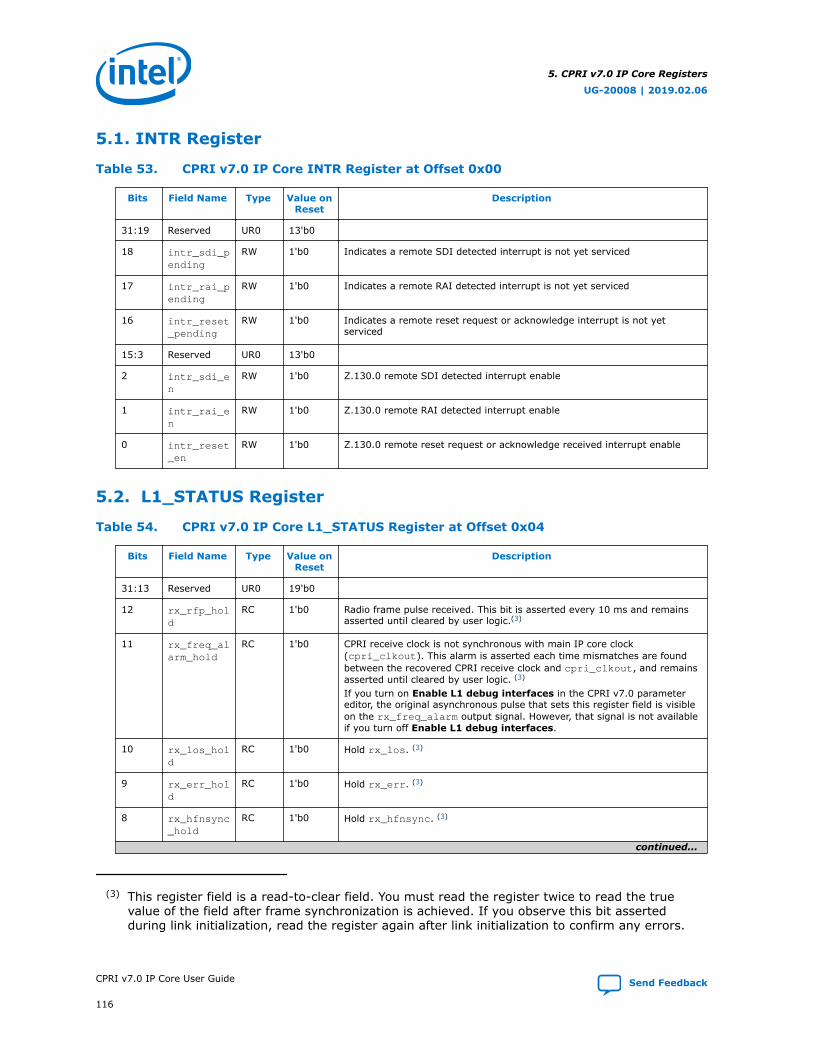
5.1. INTR Register
Table 53. CPRI v7.0 IP Core INTR Register at Offset 0x00
Bits Field Name Type Value onReset
Description
31:19 Reserved UR0 13'b0
18 intr_sdi_pending
RW 1'b0 Indicates a remote SDI detected interrupt is not yet serviced
17 intr_rai_pending
RW 1'b0 Indicates a remote RAI detected interrupt is not yet serviced
16 intr_reset_pending
RW 1'b0 Indicates a remote reset request or acknowledge interrupt is not yetserviced
15:3 Reserved UR0 13'b0
2 intr_sdi_en
RW 1'b0 Z.130.0 remote SDI detected interrupt enable
1 intr_rai_en
RW 1'b0 Z.130.0 remote RAI detected interrupt enable
0 intr_reset_en
RW 1'b0 Z.130.0 remote reset request or acknowledge received interrupt enable
5.2. L1_STATUS Register
Table 54. CPRI v7.0 IP Core L1_STATUS Register at Offset 0x04
Bits Field Name Type Value onReset
Description
31:13 Reserved UR0 19'b0
12 rx_rfp_hold
RC 1'b0 Radio frame pulse received. This bit is asserted every 10 ms and remainsasserted until cleared by user logic.(3)
11 rx_freq_alarm_hold
RC 1'b0 CPRI receive clock is not synchronous with main IP core clock(cpri_clkout). This alarm is asserted each time mismatches are foundbetween the recovered CPRI receive clock and cpri_clkout, and remainsasserted until cleared by user logic. (3)
If you turn on Enable L1 debug interfaces in the CPRI v7.0 parametereditor, the original asynchronous pulse that sets this register field is visibleon the rx_freq_alarm output signal. However, that signal is not availableif you turn off Enable L1 debug interfaces.
10 rx_los_hold
RC 1'b0 Hold rx_los. (3)
9 rx_err_hold
RC 1'b0 Hold rx_err. (3)
8 rx_hfnsync_hold
RC 1'b0 Hold rx_hfnsync. (3)
continued...
(3) This register field is a read-to-clear field. You must read the register twice to read the truevalue of the field after frame synchronization is achieved. If you observe this bit assertedduring link initialization, read the register again after link initialization to confirm any errors.
5. CPRI v7.0 IP Core Registers
UG-20008 | 2019.02.06
CPRI v7.0 IP Core User Guide Send Feedback
116
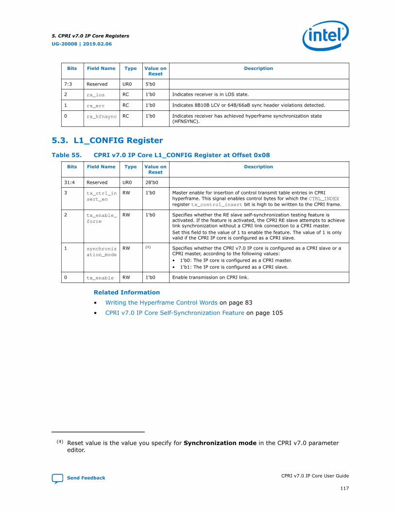
Bits Field Name Type Value onReset
Description
7:3 Reserved UR0 5'b0
2 rx_los RC 1'b0 Indicates receiver is in LOS state.
1 rx_err RC 1'b0 Indicates 8B10B LCV or 64B/66aB sync header violations detected.
0 rx_hfnsync RC 1'b0 Indicates receiver has achieved hyperframe synchronization state(HFNSYNC).
5.3. L1_CONFIG Register
Table 55. CPRI v7.0 IP Core L1_CONFIG Register at Offset 0x08
Bits Field Name Type Value onReset
Description
31:4 Reserved UR0 28'b0
3 tx_ctrl_insert_en
RW 1'b0 Master enable for insertion of control transmit table entries in CPRIhyperframe. This signal enables control bytes for which the CTRL_INDEXregister tx_control_insert bit is high to be written to the CPRI frame.
2 tx_enable_force
RW 1'b0 Specifies whether the RE slave self-synchronization testing feature isactivated. If the feature is activated, the CPRI RE slave attempts to achievelink synchronization without a CPRI link connection to a CPRI master.Set this field to the value of 1 to enable the feature. The value of 1 is onlyvalid if the CPRI IP core is configured as a CPRI slave.
1 synchronization_mode
RW (4) Specifies whether the CPRI v7.0 IP core is configured as a CPRI slave or aCPRI master, according to the following values:• 1'b0: The IP core is configured as a CPRI master.• 1'b1: The IP core is configured as a CPRI slave.
0 tx_enable RW 1'b0 Enable transmission on CPRI link.
Related Information
• Writing the Hyperframe Control Words on page 83
• CPRI v7.0 IP Core Self-Synchronization Feature on page 105
(4) Reset value is the value you specify for Synchronization mode in the CPRI v7.0 parametereditor.
5. CPRI v7.0 IP Core Registers
UG-20008 | 2019.02.06
Send Feedback CPRI v7.0 IP Core User Guide
117

5.4. BIT_RATE_CONFIG Register
Table 56. CPRI v7.0 IP Core BIT_RATE_CONFIG Register at Offset 0x0C
Bits Field Name Type Value onReset
Description
31:5 Reserved UR0 27'b0
4:0 bit_rate (5) (6) CPRI line bit rate to be used in next attempt to achieve framesynchronization, encoded according to the following valid values:• 6'b000001: 0.6144 Gbps• 6'b000010: 1.2288 Gbps• 6'b000100: 2.4576 Gbps• 6'b000101: 3.0720 Gbps• 6'b001000: 4.9150 Gbps• 6'b001010: 6.1440 Gbps• 6'b010110: 8.11008 Gbps• 6'b010000: 9.8304 Gbps• 6'b010100: 10.1376 Gbps• 6b'011000: 12.16512 Gbps• 6'b110000 : 24.33024 GbpsIf the input signal nego_bitrate_in has a non-zero value, the CPRI v7.0IP core uses the encoded value driven on nego_bitrate_in in the nextattempt to achieve frame synchronization, and ignores the value in thebit_rate register field.The value driven on the nego_bitrate_in signal, if it is non-zero, alwaysoverrides the value in this register field.
Related Information
Auto-Rate Negotiation on page 85
5.5. PROT_VER Register
Table 57. CPRI v7.0 IP Core PROT_VER Register at Offset 0x10
Bits Field Name Type Value onReset
Description
31:25 Reserved UR0 7'b0
24 rx_prot_ver_valid
RO 1'b0 Value received in incoming Z.2.0 control byte is a valid CPRI v7.0 protocolversion encoding.
23:16 rx_prot_ver
RO 8'b0 Encoded protocol version received in incoming Z.2.0 control byte.
15:10 Reserved UR0 6'b0
9 prot_ver_auto
RW 1'b1 Enables auto negotiation of protocol version.
RO 1'b0
continued...
(5) If you turn on Enable line bit rate auto-negotiation, this register field is a RW registerfield. If you turn off Enable line bit rate auto-negotiation, this register field is a RO registerfield.
(6) Reset value is the value you specify for Line bit rate in the CPRI v7.0 parameter editor.
5. CPRI v7.0 IP Core Registers
UG-20008 | 2019.02.06
CPRI v7.0 IP Core User Guide Send Feedback
118

Bits Field Name Type Value onReset
Description
If you turn on Enable protocol version and C&M channel setting auto-negotiation, this field is a RW register field with the default value of 1.Otherwise, this field is a RO register field with the default value of 0.
8 rx_prot_ver_filter
RW 1'b1 Enable filtering or protection of the Z.2.0 value across five consecutivehyperframes.If you turn on Enable protocol version and C&M channel setting auto-negotiation, this field is a RW register field with the default value of 1.Otherwise, this field is a RO register field with the default value of 0.
RO 1'b0
7:0 tx_prot_ver
RW 8'b01 Transmit protocol version to be mapped to Z.2.0 to indicate whether or notthe current hyperframe transmission is scrambled. The value 1 indicates itis not scrambled and the value 2 indicates it is scrambled.If the prot_ver_auto field has the value of 1, the IP core automaticallyupdates the tx_prot_ver field.
5.6. TX_SCR Register
Table 58. CPRI v7.0 IP Core TX_SCR Register at Offset 0x14
Bits Field Name Type Value onReset
Description
31 Reserved UR0 1'b0
30:0 tx_scr_seed
RW 31'b0 Transmitter scrambler seed. If the seed has value 0, the transmission is notscrambled.
5.7. RX_SCR Register
Table 59. CPRI v7.0 IP Core RX_SCR Register at Offset 0x18
Bits Field Name Type Value onReset
Description
31 rx_scr_active
RO 1'b0 Indicates that the incoming hyperframe is scrambled. The value 1 indicatesthat the incoming communication is scrambled, and the value 0 indicatesthat it is not scrambled. The IP core determines whether or not theincoming communication is scrambled based on the protocol version.
30:0 rx_scr_seed
RO 31'b0 Received scrambler seed. The receiver descrambles the incoming CPRIcommunication based on this seed.
5.8. CM_CONFIG Register
Table 60. CPRI v7.0 IP Core CM_CONFIG Register at Offset 0x1C
Bits Field Name Type Value onReset
Description
31:13 Reserved UR0 19'b0
12 slow_cm_rate_auto
RW 1'b1 Enable auto-negotiation of HDLC rate.If you turn on Enable protocol version and C&M channel setting auto-negotiation, this field is a RW register field with the default value of 1.Otherwise, this field is a RO register field with the default value of 0.
RO 1'b0
continued...
5. CPRI v7.0 IP Core Registers
UG-20008 | 2019.02.06
Send Feedback CPRI v7.0 IP Core User Guide
119

Bits Field Name Type Value onReset
Description
11 slow_cm_rate_filter
RW 1'b1 Enable filtering of HDLC rate.
10:8 tx_slow_cm_rate
RW 3'b110 Rate configuration for slow Control and Management (HDLC). To be insertedin CPRI control byte Z.66.0.
7 fast_cm_ptr_auto
RW 1'b1 Enable auto-negotiation of Ethernet rate.If you turn on Enable protocol version and C&M channel setting auto-negotiation, this field is a RW register field with the default value of 1.Otherwise, this field is a RO register field with the default value of 0.
RO 1'b0
6 fast_cm_ptr_filter
RW 1'b1 Enable filtering of Ethernet rate.
5:0 tx_fast_cm_ptr
RW 6'd20 Pointer to first CPRI control word used for fast Control and Management(Ethernet). To be inserted in CPRI control byte Z.194.0.
5.9. CM_STATUS Register
Table 61. CPRI v7.0 IP Core CM_STATUS Register at Offset 0x20
Bits Field Name Type Value onReset
Description
31:12 Reserved UR0 20'b0
11 rx_slow_cm_rate_valid
RO 1'b0 Indicates that a valid HDLC rate has been accepted.
10:8 rx_slow_cm_rate
RO 3'b0 Accepted received HDLC rate. The IP core receives this rate in the incomingZ.66.0 control byte.
7 Reserved UR0 1'b0
6 rx_fast_cm_ptr_valid
RO 1'b0 Indicates that a valid Ethernet rate has been accepted. The IP core receivesthis rate in the incoming Z.194.0 control byte.
5:0 rx_fast_cm_ptr
RO 6'b0 Accepted received Ethernet rate.Valid values are between 0x14 (decimal 20) and 0x3F (decimal 63),inclusive.
5.10. START_UP_SEQ Register
Table 62. CPRI v7.0 IP Core START_UP_SEQ Register at Offset 0x24This register is available only if you turn on Enable start-up sequence state machine in the CPRI v7.0parameter editor.
Bits Field Name Type Value onReset
Description
31:17 Reserved UR0 15'b0
16 startup_timer_expired
RO 1'b0 Indicates that the internal L1 start-up timer is expired, based on the valueof the startup_timer_period field of the START_UP_TIMER register.
15:11 Reserved UR0 5'b0
continued...
5. CPRI v7.0 IP Core Registers
UG-20008 | 2019.02.06
CPRI v7.0 IP Core User Guide Send Feedback
120

Bits Field Name Type Value onReset
Description
10:8 state_startup_seq
RO 3'b0 Indicates the current state of the start-up sequence. This field has thefollowing valid values:• 3'b000: State A: Standby• 3'b001: State B: L1 Synchronization• 3'b011: State C: Protocol Setup• 3'b010: State D: Control and Management Setup• 3'b110: State E: Interface and VSS Negotiation• 3'b111: State F: Operation• 3'b101: State G: Passive Link
7:4 Reserved UR0 4'b0
3 nego_vss_complete
RW 1'b0 Indicates the Vendor Specific negotiation is complete. You must set this bitto move the start-up sequence state machine from state E to state F. If youturn on Enable start-up sequence state machine, thenego_vss_complete input signal writes directly to this register bit.
2 nego_cm_complete
RW 1'b0 Indicates the Control and Management negotiation is complete and thestart-up sequence state machine can move from state D to state E. If theslow_cm_rate_auto field or the fast_cm_ptr_auto field, or both, inthe CM_CONFIG register has the value of 1, the IP core updates this bit ifthe user does not update it.If you turn on Enable start-up sequence state machine, thenego_cm_complete input signal writes directly to this register bit.Note: If the Control and Management negotiation cannot complete
successfully, per Figure 30 in the CPRI specification v7.0(2013-08-30), the start-up sequence state machine moves fromstate D to state G. In that case the IP core does not set thenego_cm_complete bit, and the state_startup_seq fieldreflects the state change.
1 nego_protocol_complete
RW 1'b0 Indicates the protocol version negotiation is complete and the start-upsequence state machine can move from state C to state D. If theprot_ver_auto field of the PROT_VER register has the value of 1, the IPcore updates this bit if the user does not update it.If you turn on Enable start-up sequence state machine, thenego_protocol_complete input signal writes directly to this register bit.
0 nego_bitrate_complete
RW 1'b0 Indicates the CPRI line bit rate negotiation is complete.If you turn on Enable start-up sequence state machine, thenego_bitrate_complete input signal writes directly to this register bit.
5.11. START_UP_TIMER Register
Table 63. CPRI v7.0 IP Core START_UP_TIMER Register at Offset 0x28This register is available only if you turn on Enable start-up sequence state machine in the CPRI v7.0parameter editor.
Bits Field Name Type Value onReset
Description
31:20 Reserved UR0 12'b0
19:0 startup_timer_period
RW 20'b0 Threshold value for L1 start-up timer to expire. The unit is cpri_coreclkclock cycles.
5. CPRI v7.0 IP Core Registers
UG-20008 | 2019.02.06
Send Feedback CPRI v7.0 IP Core User Guide
121

5.12. FLSAR Register
Table 64. CPRI v7.0 IP Core FLSAR Register at Offset 0x2CThe FLSAR register is the L1 inband control word Z.130.0 control and status register.
Bits Field Name Type Value onReset
Description
31 Reserved UR0 1'b0
30 local_lof RO 1'b0 Local loss of frame (LOF) detected
29 local_los RO 1'b0 Local loss of signal (LOS) detected
28 lof_detected
RO 1'b0 Remote LOF detected
27 los_detected
RO 1'b0 Remote LOS detected
26 sdi_detected
RO 1'b0 Remote service access point (SAP) defect indication (SDI) detected.
25 rai_detected
RO 1'b0 Remote alarm indication (RAI) detected.
24 reset_detected
RO 1'b0 Reset request or acknowledgement detected.
23:17 Reserved UR0 7'b0
16 sdi_gen RW 1'b0 Enable Z.130.0 SDI generation.
15:9 Reserved UR0 7'b0
8 rai_gen RW 1'b1 Enable Z.130.0 RAI generation as a result of local loss of signal (LOS) orloss of frame (LOF).
7:1 Reserved UR0 7'b0
0 reset_gen RW 1'b0 Enable Z.130.0 reset generation.
Related Information
Direct L1 Control and Status Interface on page 70
5.13. CTRL_INDEX Register
Table 65. CPRI v7.0 IP Core CTRL_INDEX Register at Offset 0x30Frequency differences between the control and status interface clock cpu_clk and the main CPRI v7.0 IP coreclock cpri_clkout might cause non-zero read latency and more than one clock cycle of write latency whenaccessing this register.
Bits Field Name Type Value onReset
Description
31:27 Reserved UR0 5'b0
26:24 rx_ctrl_seq
RW 3'b0 Sequence number for CPRI control word 32-bit section monitoring. Thevalue in this field determines the 32-bit section of the control receive tableentry that appears in the RX_CTRL register. The value indicates whetherthis is the first, second, third, fourth, or fifth (for RTVS) 32-bit section inthe control word.
continued...
5. CPRI v7.0 IP Core Registers
UG-20008 | 2019.02.06
CPRI v7.0 IP Core User Guide Send Feedback
122

Bits Field Name Type Value onReset
Description
23:16 rx_ctrl_x RW 8'b0 Index for CPRI control word monitoring (X value in frame location #Z.X.Y).The value in this field determines the control receive table entry of which a32-bit section appears in the RX_CTRL register.
15:12 Reserved UR0 4'b0
11 tx_ctrl_insert
RW 1'b0 Control word 32-bit section transmit enable. This value is stored in thecontrol transmit table with its associated entry. When you change the valueof the tx_ctrl_seq field or the tx_ctrl_x field, the storedtx_ctrl_insert bit associated with the indexed entry appears in thetx_ctrl_insert field.At the time the CPRI v7.0 IP core can insert a control transmit table entryin the associated position in the outgoing hyperframe on the CPRI link, ifthe tx_ctrl_insert bit associated with that entry has the value of 1, andthe tx_ctrl_insert_en bit of the L1_CONFIG register is asserted, the IPcore inserts the table entry in the hyperframe.
10:8 tx_ctrl_seq
RW 3'b0 Sequence number for CPRI control word 32-bit section insertion. The valuein this field determines the 32-bit section of the control transmit table entrythat appears in the TX_CTRL register. The value indicates whether this isthe first, second, third, fourth, or fifth (for RTVS) 32-bit section in thecontrol word.
7:0 tx_ctrl_x RW 8'b0 Index for CPRI control word insertion (X value in frame location #Z.X.Y).The value in this field determines the control transmit table entry of which a32-bit section appears in the TX_CTRL register.
5.14. TX_CTRL Register
Table 66. CPRI v7.0 IP Core TX_CTRL Register at Offset 0x34Frequency differences between the control and status interface clock cpu_clk and the main CPRI v7.0 IP coreclock cpri_clkout might cause non-zero read latency and more than one clock cycle of write latency whenaccessing this register.
Bits Field Name Type Value onReset
Description
31:0 tx_ctrl_data
RW 32'b0 CPRI control word 32-bit section to be transmitted in CPRI hyperframeposition Z.x, where x is the index in the tx_ctrl_x field of theCTRL_INDEX register. The tx_ctrl_seq field of the CTRL_INDEX registerindicates whether this is the first, second, third, fourth, or fifth such 32-bitsection.
5.15. RX_CTRL Register
Table 67. CPRI v7.0 IP Core RX_CTRL Register at Offset 0x38Frequency differences between the control and status interface clock cpu_clk and the main CPRI v7.0 IP coreclock cpri_clkout might cause non-zero read latency and more than one clock cycle of write latency whenaccessing this register.
Bits Field Name Type Value onReset
Description
31:0 rx_ctrl_data
RO 32'b0 Most recent received CPRI control word 32-bit section from CPRIhyperframe position Z.x, where x is the index in the rx_ctrl_x field of theCTRL_INDEX register. The rx_ctrl_seq field of the CTRL_INDEX registerindicates whether this is the first, second, third, fourth, or fifth such 32-bitsection.
5. CPRI v7.0 IP Core Registers
UG-20008 | 2019.02.06
Send Feedback CPRI v7.0 IP Core User Guide
123
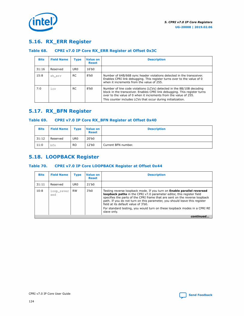
5.16. RX_ERR Register
Table 68. CPRI v7.0 IP Core RX_ERR Register at Offset 0x3C
Bits Field Name Type Value onReset
Description
31:16 Reserved UR0 16'b0
15:8 sh_err RC 8'b0 Number of 64B/66B sync header violations detected in the transceiver.Enables CPRI link debugging. This register turns over to the value of 0when it increments from the value of 255.
7:0 lcv RC 8'b0 Number of line code violations (LCVs) detected in the 8B/10B decodingblock in the transceiver. Enables CPRI link debugging. This register turnsover to the value of 0 when it increments from the value of 255.This counter includes LCVs that occur during initialization.
5.17. RX_BFN Register
Table 69. CPRI v7.0 IP Core RX_BFN Register at Offset 0x40
Bits Field Name Type Value onReset
Description
31:12 Reserved UR0 20'b0
11:0 bfn RO 12'b0 Current BFN number.
5.18. LOOPBACK Register
Table 70. CPRI v7.0 IP Core LOOPBACK Register at Offset 0x44
Bits Field Name Type Value onReset
Description
31:11 Reserved UR0 21'b0
10:8 loop_reversed
RW 3'b0 Testing reverse loopback mode. If you turn on Enable parallel reversedloopback paths in the CPRI v7.0 parameter editor, this register fieldspecifies the parts of the CPRI frame that are sent on the reverse loopbackpath. If you do not turn on this parameter, you should leave this registerfield at its default value of 3'b0.For standard testing, you would turn on these loopback modes in a CPRI REslave only.
continued...
5. CPRI v7.0 IP Core Registers
UG-20008 | 2019.02.06
CPRI v7.0 IP Core User Guide Send Feedback
124

Bits Field Name Type Value onReset
Description
This field has the following valid values:• 3'b000: No loopback.• 3'b001: Full CPRI frame loopback. Incoming CPR data and control words
are sent back as-is in outgoing CPR communication.• 3'b010: I/Q data loopback. Incoming CPRI data are sent back in
outgoing CPRI communication; control words are generated locally.• 3'b011: Fast control and management loopback. Incoming CPRI fast
control and management (Ethernet) control and data words are sentback in outgoing CPRI communication; remaining data and controlwords are generated locally.
• 3'b100: Fast control and management and VS loopback. Incoming CPRIfast control and management (Ethernet) and vendor-specific controlwords are sent back in outgoing CPRI communication; data andremaining control words are generated locally.
7:2 Reserved UR0 6'b0
1:0 loop_forward
RW 2'b0 Testing forward loopback mode. If you turn on Enable transceiver PMAserial forward loopback path or Enable parallel forward loopbackpaths in the CPRI v7.0 parameter editor, this register field specifies theloopback path that is currently active. If you do not turn on either of theseparameters, you should leave this register field at its default value of 2'b0.This field has the following valid values:• 2'b00: No loopback.• 2'b01: Transceiver PMA loopback path is active. This path does not
exercise the transceiver PCS. This option is available only if you turn onEnable transceiver PMA serial forward loopback path .
• 2'b10: Active loopback path includes extended delay measurement logicbut does not exercise the transceiver. This option is available only if youturn on Enable parallel forward loopback paths.
• 2'b11: Active loopback path includes framing and deframing logic, butdoes not exercise the extended delay measurement logic and does notexercise the transceiver. This option is available only if you turn onEnable parallel forward loopback paths.
Related Information
CPRI v7.0 IP Core Loopback Modes on page 105
5.19. TX_DELAY Register
Table 71. CPRI v7.0 IP Core TX_DELAY Register at Offset 0x48
Bits Field Name Type Value onReset
Description
31:9 Reserved UR0 23'b0
8 tx_buf_resync
RW 1'b0 Force transmit buffer pointer resynchronization. You can use this registerfield to resynchronize if, for example, the buffer fill level becomes too highdue to due to environmental impacts on the device, such as temperature.Resynchronizing might lead to data loss or corruption.Do not use this register field to resynchronize after a dynamic CPRI line bitrate change. After a dynamic CPRI line bit rate change the IP core forcesresynchronization internally without referring to this register.
7:4 Reserved UR0 4'b0
3:0 tx_buf_delay
RO 4'b0 Current transmit buffer fill level.
5. CPRI v7.0 IP Core Registers
UG-20008 | 2019.02.06
Send Feedback CPRI v7.0 IP Core User Guide
125
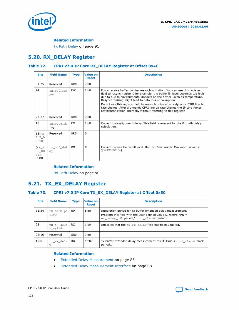
Related Information
Tx Path Delay on page 91
5.20. RX_DELAY Register
Table 72. CPRI v7.0 IP Core RX_DELAY Register at Offset 0x4C
Bits Field Name Type Value onReset
Description
31:25 Reserved UR0 7'b0
24 rx_buf_resync
RW 1'b0 Force receive buffer pointer resynchronization. You can use this registerfield to resynchronize if, for example, the buffer fill level becomes too highdue to due to environmental impacts on the device, such as temperature.Resynchronizing might lead to data loss or corruption.Do not use this register field to resynchronize after a dynamic CPRI line bitrate change. After a dynamic CPRI line bit rate change the IP core forcesresynchronization internally without referring to this register.
23:17 Reserved UR0 7'b0
16 rx_byte_delay
RO 1'b0 Current byte-alignment delay. This field is relevant for the Rx path delaycalculation.
15:RX_BUF_DEPTH
Reserved UR0 0
(RX_BUF_DEPTH-1):0
rx_buf_delay
RO 0 Current receive buffer fill level. Unit is 32-bit words. Maximum value is2RX_BUF_DEPTH-1.
Related Information
Rx Path Delay on page 90
5.21. TX_EX_DELAY Register
Table 73. CPRI v7.0 IP Core TX_EX_DELAY Register at Offset 0x50
Bits Field Name Type Value onReset
Description
31:24 tx_msrm_period
RW 8'b0 Integration period for Tx buffer extended delay measurement.Program this field with the user-defined value N, where M/N =ex_delay_clk period / cpri_clkout period.
23 tx_ex_delay_valid
RC 1'b0 Indicates that the tx_ex_delay field has been updated.
22:16 Reserved UR0 7'b0
15:0 tx_ex_delay
RO 16'b0 Tx buffer extended delay measurement result. Unit is cpri_clkout clockperiods.
Related Information
• Extended Delay Measurement on page 85
• Extended Delay Measurement Interface on page 88
5. CPRI v7.0 IP Core Registers
UG-20008 | 2019.02.06
CPRI v7.0 IP Core User Guide Send Feedback
126

5.22. RX_EX_DELAY Register
Table 74. CPRI v7.0 IP Core IRX_EX_DELAY Register at Offset 0x54
Bits Field Name Type Value onReset
Description
31:24 rx_msrm_period
RW 8'b0 Integration period for Rx buffer extended delay measurement.Program this field with the user-defined value NR, where M/NR =ex_delay_clk period / cpri_clkout period.
23 rx_ex_delay_valid
RC 1'b0 Indicates that the rx_ex_delay field has been updated.
22:RX_BUF_DEPTH
Reserved UR0 0
(RX_BUF_DEPTH-1):0
rx_ex_delay
RO 0 Rx buffer extended delay measurement result. Unit is cpri_clkout clockperiods.
Related Information
• Extended Delay Measurement on page 85
• Extended Delay Measurement Interface on page 88
5.23. ROUND_TRIP_DELAY Register
Table 75. CPRI v7.0 IP Core ROUND_TRIP_DELAY Register at Offset 0x58
Bits Field Name Type Value onReset
Description
31:20 Reserved UR0 12'b0
19:0 round_trip_delay
RO 20'b0 Measured round-trip delay from aux_tx_rfp to aux_rx_rfp. Unit iscpri_clkout clock periods. The IP core updates this field with every radioframe.
Related Information
Round-Trip Delay on page 92
5.24. XCVR_BITSLIP Register
Table 76. CPRI v7.0 IP Core XCVR_BITSLIP Register at Offset 0x5C
Bits Field Name Type Value onReset
Description
31:21 Reserved UR0 11'b0
20:16 rx_bitslip_out
RO 5'b0 Number of bits of delay (bitslip) detected at the receiver word-aligner.Value can change at frame synchronization, when the transceiver isresetting. Any K28.5 symbol position change that occurs when wordalignment is activated changes the bitslip value.
continued...
5. CPRI v7.0 IP Core Registers
UG-20008 | 2019.02.06
Send Feedback CPRI v7.0 IP Core User Guide
127

Bits Field Name Type Value onReset
Description
15:6 Reserved UR0 10'b0
5 tx_bitslip_en
RW 1'b0 Enable manual tx_bitslip_in updates.
4:0 tx_bitslip_in
RW 5'b0 Number of bits of delay (bitslip) the CPRI v7.0 IP core adds at the CPRI Txlink.The CPRI line bit rate determines the following maximum values for thisfield:• Maximum value for IP core variations with CPRI line bit rate 0.6144
Gbps: 9 bits.• Maximum value for IP core variations with CPRI line bit rate greater
than 0.6144 Gbps: 19 bits.
Related Information
Tx Bitslip Delay on page 97
5.25. DELAY_CAL_STD_CTRL1 Register
Table 77. CPRI v7.0 IP Core DELAY_CAL_STD_CTRL1 Register at Offset 0x60This register is available only in CPRI IP cores with the single-trip delay calibration feature.
Bits Field Name Type Value onReset
Description
31:17 Reserved UR0 15'b0
16 cal_reset RW 1'b0 Reset single-trip delay calibration.Set this bit to the value of 1 to reset the IP core single-trip delaycalibration module and the Intel-provided DPCU module that you haveconnected to the IP core. Reset this bit to the value of 0 to resume thenormal functionality of these two modules.Setting this bit to the value of 1 resets all of the single-trip delaycalibration logic. This reset does not affect the values in theDELAY_CAL_STD_CTRLn registers. However, the reset does override thevalue in the cal_int_check field.
15:9 Reserved UR0 7'b0
8 cal_int_check RW 1'b0 Enable single-trip delay consistency checking. If you set this bit to thevalue of 1, the IP core checks once per hyperframe that the sum of thecal_step_delay and cal_cycle_delay field values in theDELAY_CAL_STD_CTRL2 register match the cal_current_delay fieldvalue in the DELAY_CAL_STD_STATUS register. If they do not match, theIP core triggers recalibration.If you set this bit to the value of 0, the IP core performs a consistencycheck only when you set the cal_en bit. If cal_int_check has thevalue of 0, the user can schedule consistency checks by resetting andsetting the cal_en bit.
7:1 Reserved UR0 7'b0
0 cal_en RW 1'b0 Enable single-trip delay calibration.Set this bit to the value of 1 to activate single-trip delay calibration. Resetthis bit to the value of 0 to turn off single-trip delay calibration.
5. CPRI v7.0 IP Core Registers
UG-20008 | 2019.02.06
CPRI v7.0 IP Core User Guide Send Feedback
128

5.26. DELAY_CAL_STD_CTRL2 Register
Table 78. CPRI v7.0 IP Core DELAY_CAL_STD_CTRL2 Register at Offset 0x64This register is available only in CPRI slave IP cores with the single-trip delay calibration feature.
The user provides this information to specify the anticipated or desired duration of the total variable componentof the single-trip delay. This value reflects the system requirements.
Bits Field Name Type Value onReset
Description
31:25 Reserved UR0 7'b0
24:16 cal_step_delay
RW 9'b0 Additional fractional cpri_clkout clock cycles of delay in step units.
15:8 Reserved UR0 8'b0
7:0 cal_cycle_delay
RW 8'b0 Delay in full cpri_clkout clock cycles.
5.27. DELAY_CAL_STD_CTRL3 Register
Table 79. CPRI v7.0 IP Core DELAY_CAL_STD_CTRL3 Register at Offset 0x68This register is available only in CPRI master IP cores with the single-trip delay calibration feature.
Bits Field Name Type Value onReset
Description
31:17 Reserved UR0 15'b0
16 cal_send_en
RW 1'b0 Enable a CPRI master IP core to include TX delay information in outgoingCPRI communication.Software must specify the location of this information in the transmittedradio frame by writing the location information in the cal_send_seq andcal_send_x fields.
15 Reserved UR0 1'b0
14:8 cal_send_seq
RW 7'b0 In a CPRI master IP core, specifies the sequence number in the outgingbasic frame that is the location of the TX delay information the IP coreprovides to the receiving CPRI slave.Note: If the CPRI slave that receives CPRI communication from this IP
core on the CPRI link is an Intel FPGA CPRI v7.0 IP core, the valuein this field must be identical to the value in the cal_rcv_seq fieldof the DELAY_CAL_STD_CTRL4 register in that CPRI slave.
7:0 cal_send_x RW 8'b0 In a CPRI master IP core, specifies the basic frame number in the incominghyperframe that is the location of the TX delay information the IP coreprovides to the receiving CPRI slave.Note: If the CPRI slave that receives CPRI communication from this IP
core on the CPRI link is an Intel FPGA CPRI v7.0 IP core, the valuein this field must be identical to the value in the cal_rcv_x field ofthe DELAY_CAL_STD_CTRL4 register in that CPRI slave.
5. CPRI v7.0 IP Core Registers
UG-20008 | 2019.02.06
Send Feedback CPRI v7.0 IP Core User Guide
129

5.28. DELAY_CAL_STD_CTRL4 Register
Table 80. CPRI v7.0 IP Core DELAY_CAL_STD_CTRL4 Register at Offset 0x6CThis register is available only in CPRI slave IP cores with the single-trip delay calibration feature.
Bits Field Name Type Value onReset
Description
31:17 Reserved UR0 15'b0
16 cal_rcv_en RW 1'b0 Enable a CPRI slave IP core to receive TX delay information in incomingCPRI communication.Software must specify the location of this information in the incoming radioframe by writing the location information in the cal_rcv_seq andcal_rcv_x fields.The cal_tx_delay_usr_en field of the DELAY_CAL_STD_CTRL5 registeroverrides this register field.
15 Reserved UR0 1'b0
14:8 cal_rcv_seq
RW 7'b0 In a CPRI slave IP core, specifies the sequence number in the incomingbasic frame that is the location of the TX delay information provided by thetransmitting CPRI master.Note: If the CPRI master that transmits to this IP core on the CPRI link is
an Intel FPGA CPRI v7.0 IP core, the value in this field must beidentical to the value in the cal_send_seq field of theDELAY_CAL_STD_CTRL3 register in that CPRI master.
7:0 cal_rcv_x RW 8'b0 In a CPRI slave IP core, specifies the basic frame number in the incominghyperframe that is the location of the TX delay information provided by thetransmitting CPRI master.Note: If the CPRI master that transmits to this IP core on the CPRI link is
an Intel FPGA CPRI v7.0 IP core, the value in this field must beidentical to the value in the cal_send_x field of theDELAY_CAL_STD_CTRL3 register in that CPRI master.
5.29. DELAY_CAL_STD_CTRL5 Register
Table 81. CPRI v7.0 IP Core DELAY_CAL_STD_CTRL5 Register at Offset 0x70This register is available only in CPRI slave IP cores with the single-trip delay calibration feature.
Bits Field Name Type Value onReset
Description
31:17 Reserved UR0 15'b0
16 cal_tx_delay_usr_en
RW 1'b0 Enable a CPRI slave IP core to receive TX delay information in thecal_tx_delay_usr field.When the value of this field is 1, the IP core cannot receive TX delayinformation in incoming CPRI communication.
15:12 Reserved UR0 4'b0
11:0 cal_tx_delay_usr
RW 12'b0 TX delay value provided by software. This field is valid only when thecal_tx_delay_usr_en field has the value of 1.Unit is clk_ex_delay clock cycles.
5. CPRI v7.0 IP Core Registers
UG-20008 | 2019.02.06
CPRI v7.0 IP Core User Guide Send Feedback
130

5.30. DELAY_CAL_STD_STATUS Register
Table 82. CPRI v7.0 IP Core DELAY_CAL_STD_STATUS Register at Offset 0x74This register is available only in CPRI slave IP cores with the single-trip delay calibration feature.
Bits Field Name Type Value onReset
Description
31:16 Reserved UR0 16'b0
15:0 cal_current_delay
RO 16'b0 Variable delay from the synchronization service access point (SAP) in theCPRI link master to the synchronization SAP in this CPRI v7.0 slave IP core.Unit is clk_ex_delay clock cycles.The IP core calculates this value. The Intel-provided single-trip delaycalibration modules use this value to determine the values they write to thecal_step_delay and cal_cycle_delay fields of the IP core'sDELAY_CAL_STD_CTRL2 register.
5.31. DELAY_CAL_RTD Register
Table 83. CPRI v7.0 IP Core DELAY_CAL_RTD Register at Offset 0x80This register is available only in CPRI master IP cores with the single-trip delay calibration feature.
Bits Field Name Type Value onReset
Description
31:30 Reserved UR0 2'b0
29:28 cal_rtd_status
RW 2'b0 Round trip delay calibration status. Valid values are:• 00: Calibration is turned off.• 01: Calibration is running.• 11: Error: IP core is unable to meet the calibration requirement.• 10: Calibration has completed or is in the monitoring stage.
27 Reserved UR0 1'b0
26:24 cal_rtd_ctrl
RW 3'b0 Round trip delay calibration control. Valid values are one-hot:• Bit [26]: Active high reset bit that resets the calibration block. Use this
bit to reset the calibration block after an error or to re-enable thecalibration block to take it out of bypass mode.
• Bit [25]: Enable or disable calibration block bypass mode. When thevalue of this bit is 1, round trip delay calibration is in bypass mode.When the value of this bit is 0, round trip delay calibration is not inbypass mode.
• Bit [24]: Enable or disable round trip delay calibration. When the valueof this bit is 1, round trip delay calibration is turned on. When the valueof this bit is 0, round trip delay calibration is turned off.
23:20 Reserved UR0 4'b0
19:0 cal_rtd_usr
RW 20'b0 Desired round-trip delay value. Unit is cpri_clkout cycles.
5. CPRI v7.0 IP Core Registers
UG-20008 | 2019.02.06
Send Feedback CPRI v7.0 IP Core User Guide
131

5.32. XCVR_TX_FIFO_DELAY Register
Table 84. CPRI v7.0 IP Core XCVR_TX_FIFO_DELAY Register at Offset 0x84This register is present only in IP core variations that target an Intel Stratix 10 device.
Bits Field Name Type Value onReset
Description
31 tx_pcs_fifo_delay_valid
RO 1'b0 Indicates that the
tx_pcs_fifo_delay
field has been updated.
30:25 Reserved UR0 6'b0
24:16 tx_pcs_fifo_delay
RO 9'b0 Delay count value for the transmitter PCS FIFO. Unit is multiples of 128/latency_sclk clock cycles (no units). In other words, the latency throughthe FIFO is <latency_sclk period>x <this field value: delay count>/128.
15 tx_core_fifo_delay_valid
RO 1'b0 Indicates that the
tx_core_fifo_delay
field has been updated.
14:9 Reserved UR0 6'b0
8:0 tx_core_fifo_delay
RO 9'b0 Delay count value for the transmitter core FIFO. Unit is multiples of 128/latency_sclk clock cycles (no units). In other words, the latency throughthe FIFO is <latency_sclk period>x <this field value: delay count>/128.
5.33. XCVR_RX_FIFO_DELAY Register
Table 85. CPRI v7.0 IP Core XCVR_RX_FIFO_DELAY Register at Offset 0x88This register is present only in IP core variations that target an Intel Stratix 10 device.
Bits Field Name Type Value onReset
Description
31 rx_pcs_fifo_delay_valid
RO 1'b0 Indicates that the
rx_pcs_fifo_delay
field has been updated.
30:25 Reserved UR0 6'b0
24:16 rx_pcs_fifo_delay
RO 9'b0 Delay count value for the receiver PCS FIFO. Unit is multiples of 128/latency_sclk clock cycles (no units). In other words, the latency throughthe FIFO is <latency_sclk period>x <this field value: delay count>/128.
15 rx_core_fifo_delay_valid
RO 1'b0 Indicates that the
rx_core_fifo_delay
field has been updated.
14:9 Reserved UR0 6'b0
8:0 rx_core_fifo_delay
RO 9'b0 Delay count value for the receiver core FIFO. Unit is multiples of 128/latency_sclk clock cycles (no units). In other words, the latency throughthe FIFO is <latency_sclk period>x <this field value: delay count>/128.
5. CPRI v7.0 IP Core Registers
UG-20008 | 2019.02.06
CPRI v7.0 IP Core User Guide Send Feedback
132
A. Additional Information
A.1. CPRI v7.0 IP Core User Guide ArchivesIf an IP core version is not listed, the user guide for the previous IP core version applies.
IP Core Version User Guide
17.0 CPRI v6.0 IP Core User Guide
16.0 CPRI v6.0 MegaCore Function User Guide
15.0 CPRI v6.0 MegaCore Function User Guide
14.0 and 14.0 Arria 10Edition
CPRI v6.0 MegaCore Function User Guide
A.2. Document Revision History for the CPRI v7.0 IP Core UserGuide
Document Version Intel QuartusPrime Version
Changes
2019.02.06 17.1 Changed the pdf filename from ug_cpri_70.pdf to ug_cpri.pdf
2019.01.28 17.1 • Added support for Intel Stratix 10 devices with H- and L-tiletransceivers.
• Intel Stratix 10 device support is now available in 17.1 Intel QuartusPrime Pro Edition software.
• Added Intel Stratix 10 device family support for new CPRI line bit ratesof 12.16512 and 24.33024 Gbps.
• Updated release information and resource utilization numbers for the17.1 software release.
• Added new parameter Data path width in Table: General CPRI v7.0 IPCore Parameters.
• Added new hybrid core clock source input.• Enable line bit rate auto-negotiation parameter is now available for
Intel Stratix 10 and Intel Arria 10 devices.• Modified Running the Testbench section.• Added cpri_clkout frequency value for 12.16512 and 24.33024 Gbps
CPRI line rates.• Clarified the value of xcvr_recovered_clk for different CPRI line bit
rates.• Added new diagrams Figure: CPRI v7.0 Master IP Core in Internal
Clocking Mode and Figure: CPRI v7.0 Slave IP Core in Internal ClockingMode.
continued...
UG-20008 | 2019.02.06
Send Feedback
Intel Corporation. All rights reserved. Intel, the Intel logo, Altera, Arria, Cyclone, Enpirion, MAX, Nios, Quartusand Stratix words and logos are trademarks of Intel Corporation or its subsidiaries in the U.S. and/or othercountries. Intel warrants performance of its FPGA and semiconductor products to current specifications inaccordance with Intel's standard warranty, but reserves the right to make changes to any products and servicesat any time without notice. Intel assumes no responsibility or liability arising out of the application or use of anyinformation, product, or service described herein except as expressly agreed to in writing by Intel. Intelcustomers are advised to obtain the latest version of device specifications before relying on any publishedinformation and before placing orders for products or services.*Other names and brands may be claimed as the property of others.
ISO9001:2015Registered

Document Version Intel QuartusPrime Version
Changes
• Modified the width of the signal auxN_rx_seq[6:0].• Changed the encoding values for all the CPRI line rates.• Modified signal names in following sections:
— AUX Interface— Direct IQ Interface— ctrl_AxC Interface— Direct Vendor Specific Access Interface— Real-Time Vendor Specific Interface
Table 86. Document Revision History
Date CompatibleACDS
Version
Changes
2018.01.04 17.0 IR3,17.0, 17.0Update 1,and 17.0Update 2
• Updated for the 17.0 software release, including Intel rebranding. Refer to Installationand Licensing on page 12, Generating CPRI v7.0 IP Cores on page 13, and CPRI v7.0 IPCore File Structure on page 14.
• Added Stratix 10 device family support for CPRI line bit rates of 1.2288 Gbps through10.1376 Gbps. Because Stratix 10 device support is not available in the Intel QuartusPrime Pro Edition releases v17.0, v17.0 Update 1, and v17.0 Update 2, this version ofthe IP core provides Stratix 10 device support only in the Intel Quartus Prime ProEdition software v17.0 IR3. Auto-rate negotiation and simplex modes are not yetavailable for CPRI IP core variations that target a Stratix 10 device.
• Updated speed grade support table in CPRI v7.0 IP Core Performance: Device andTransceiver Speed Grade Support on page 8.— Added Stratix 10 support.— Added previously missing speed grade information for Arria V GZ devices at CPRI
line rate 9.8304 Gbps.— Removed Arria 10 support for the CPRI line rate of 0.6144 Gbps. In the 17.0.260
release, the IP core no longer supports the CPRI line rate of 0.6144 Gbps for Arria10 devices.
— Corrected entries for Arria V GT and Cyclone V GT devices. The previous entrieslisted speed grades that do not exist for these devices.
continued...
A. Additional Information
UG-20008 | 2019.02.06
CPRI v7.0 IP Core User Guide Send Feedback
134

Date CompatibleACDS
Version
Changes
• Updated IP core parameters. Refer to CPRI v7.0 IP Core Parameters on page 17.— Updated default value of Line bit rate parameter. Intel Arria 10 and Intel Stratix 10
devices do not support the CPRI line bit rate of 0.6144 Gbps. The new default valueis the lowest CPRI line bit rate the target device family supports: 1228.8 Mbps forIntel Arria 10 and Intel Stratix 10 device families; 614.4 Mbps (as before) for allother supported device families.
— Specified the Intel Stratix 10 device family supports only TX/RX Duplex operationmode in the 17.0.260 release.
— Moved Core clock source input parameter before Transmitter local clockdivision factor parameter.
— Specified that IP core variations that target an Intel Arria 10 or Intel Stratix 10device, with Line bit rate set to the value of 4915.2 Mbps or lower, support only thevalue of 1 for the Transmitter local clock division factor parameter. This changeis new in the 17.0.260 release.
— Specified that IP core variations that target a device family other than the Stratix Vdevice family, support only the value of 1 for the Number of receiver CDRreference clock(s) parameter.
— Added new VCCR_GXB and VCCT_GXB supply voltage for the transceiverparameter. This parameter affects the IP core only if it targets an Intel Stratix 10device.
— Specified the Recovered clock source parameter is not available for Intel Arria 10and Intel Stratix 10 devices. IP cores that target either of these device families,support only a PCS clock source for the xcvr_recovered_clk.
— Specified the Enable single-trip delay calibration parameter is only available forIntel Arria 10 devices.
— Specified the Enable line bit rate auto-negotiation parameter is not available forIP core variations that target an Intel Stratix 10 device.
• Added information about extended delay measurement for new Stratix 10 hard FIFOs.Refer to Extended Delay Measurement on page 85 and the new section Extended DelayMeasurement for Intel Stratix 10 Hard FIFOs on page 87. The new feature adds thefollowing new parameters and registers:— Two new registers, XCVR_TX_FIFO_DELAY and XCVR_RX_FIFO_DELAY. Refer to
XCVR_TX_FIFO_DELAY Register on page 132 and XCVR_RX_FIFO_DELAY Register onpage 132.
— Two new signals, latency_sclk and latency_sreset_n. Refer to CPRI v7.0 IPCore Clocking Structure on page 38, CPRI v7.0 IP Core Reset Requirements on page44, and Extended Delay Measurement Interface on page 88.
• Added new local_lof, local_los, lof_detected, and los_detected fields to theFLSAR register at offset 0x2C. This addition is new in the 16.1.275 release of the IPcore. Added relevant information to descriptions of associated direct L1 control andstatus interface signals. Refer to FLSAR Register on page 122 and to Direct L1 Controland Status Interface on page 70.
• Added new section to clarify the conditions for transitions out of State G in the start-upsequence state machine. Refer to Start-Up Sequence Following Reset on page 47.
• Renamed the old Start-Up Sequence Following Reset section to Start-Up SequenceInterface Signals on page 49. Corrected waveform in this section.
• Added example waveforms for CPU interface and transceiver reconfiguration interface.Refer to CPU Interface Signals on page 79 and Intel Arria 10 and Intel Stratix 10Transceiver Reconfiguration Interface on page 100.
• Added Ctrl_AxC Interface on page 63 section to document the signals and behavior onthis interface. This information was previously missing.
• Added L1 Debug Interface on page 73 section to document the signals on this interface.This information was previously missing.
• Corrected statement that the transceiver debug signals are available if you turn onEnable debug interface in the CPRI IP core parameter editor. The name of theparameter is Enable L1 debug interfaces.
• Corrected TX MII timing diagram in Media Independent Interface (MII) to ExternalEthernet Block on page 74 by removing extraneous HALT symbol (/F/).
continued...
A. Additional Information
UG-20008 | 2019.02.06
Send Feedback CPRI v7.0 IP Core User Guide
135

Date CompatibleACDS
Version
Changes
• Clarified that external Ethernet block must assert the mii_txen signal two cyclesbefore it presents valid data on mii_txd[3:0], to allow the IP core to insert the /J/and /K/ nibbles in outgoing CPRI communication to indicate start-of-packet. Refer to Media Independent Interface (MII) to External Ethernet Block on page 74.
• Corrected GMII example waveforms in Gigabit Media Independent Interface (GMII) toExternal Ethernet Block on page 76. Control symbol is /V/ not /FE/, and the value of thesymbol is 0x0E, not 0xFE. Also corrected text in section where appropriate.
• Corrected rows for register DELAY_CAL_STD_CTRL2 and below in Control and StatusRegister Map table in CPRI v7.0 IP Core Registers on page 114. Offsets for theseregisters were already correct in sections for individual registers, but were listedincorrectly in the Control and Status Register Map table.
• Clarified that the value in the startup_timer_period field of the START_UP_TIMERregister at offset 0x28 is the number of cpri_coreclk clock cycles to the threshold.Refer to START_UP_TIMER Register on page 121.
• Clarified that the value of the cal_rtd_ctrl field in the DELAY_CAL_RTD register atoffset 0x80 is one-hot encoded.
• Clarified origin of accepted HDLC and Ethernet rates. Refer to CM_STATUS Register onpage 120.
• Clarified that when the cal_tx_delay_usr_en field of the DELAY_CAL_STD_CTRL5register at offset 0x70 has the value of 1, this value overrides the cal_rcv_en field inthe DELAY_CAL_STD_CTRL4 register at offset 0x6C. Refer to DELAY_CAL_STD_CTRL4Register on page 130 and DELAY_CAL_STD_CTRL5 Register on page 130.
• Filled in field names for tx_ctrl_seq and tx_ctrl_x fields of CTRL_INDEX registerat offset 0x30, which were previously missing. Refer to CTRL_INDEX Register on page122.
• Corrected direction of rx_ready and tx_ready output signals from reset controller.Refer to Adding the Reset Controller on page 27.
• Added Compiling the Full Design and Programming the FPGA on page 35 section inGetting Started chapter. This section provides the location of the Synopsys DesignConstraints file (.sdc) generated with the IP core.
• Removed How to Contact and Typographic Conventions sections.• Removed Differences Between CPRI IP Core and CPRI IP Core appendix. The CPRI IP
core is not available for recent versions of the Intel Quartus Prime software.• Removed Installation and Licensing Features section, which described the OpenCore
Plus feature. Because the CPRI IP core is available from the SSLC only with a license,this feature is not relevant.
• Added new section with links to older published versions of this user guide. If acorrection was published for the same software version, only the corrected version isavailable. Refer to CPRI v7.0 IP Core User Guide Archives on page 133.
• Fixed assorted typos and minor errors.
2016.07.22 16.0 • Updated for 16.0 software release. Updated release information and resource utilizationnumbers for the 16.0 software release.
• Updated speed grade support table in CPRI IP Core Performance: Device andTransceiver Speed Grade Support.
• Added Arria 10 and Stratix V device family support for CPRI line bit rate of 8.11008Gbps. This IP core change occurred in the CPRI IP core release 15.1.258.
• Removed Arria 10 device family support for CPRI line bit rate of 0.6144 Gbps. This IPcore change occurred in the CPRI IP core release 15.1.313.
continued...
A. Additional Information
UG-20008 | 2019.02.06
CPRI v7.0 IP Core User Guide Send Feedback
136

Date CompatibleACDS
Version
Changes
• Added support for single-trip delay calibration. This IP core change is new in the CPRI IPcore release 16.0.— Added new parameters Core clock source input and Enable single-trip delay
calibration. Refer to CPRI IP Core Parameters and Running the Testbench.— Added new clocking structure, new IOPLL and DPCU blocks, and new top-level signal
tx_clkout. Refer to CPRI IP Core Clocking Structure, CPRI IP Core ManagementInterfaces, Adding the Off-Chip Clean-Up PLL, and new section Example CPRI ClockConnections in Different Clocking Modes.
— Added new IP core signals cal_status[1:0] and cal_ctrl[15:0]. Refer toAdding and Connecting the Single-Trip Delay Calibration Blocks and Single-TripLatency Measurement and Calibration Interface Signals.
— Added new registers DELAY_CAL_STD_CTRL1, DELAY_CAL_STD_CTRL2,DELAY_CAL_STD_CTRL3, DELAY_CAL_STD_CTRL4, DELAY_CAL_STD_CTRL5, andDELAY_CAL_STD_STATUS. Refer to CPRI IP Core Registers.
— Added description of new features in new sections Delay Calibration Features andSingle-trip Delay Calibration.
• Added support for round-trip latency calibration. This IP core change is new in the CPRIIP core release 16.0.— Added new parameters Enable round-trip delay calibration and Round-trip
delay calibration FIFO depth. Refer to CPRI IP Core Parameters and Running theTestbench.
— Added new register DELAY_CAL_RTD. Refer to DELAY_CAL_RTD Register.— Added description of new features in new section Round-Trip Delay Calibration.
• Added parameters to control Avalon-MM CPU interface addressing mode and to enableADME support. Refer to CPRI IP Core Parameters. This IP core change occurred in theCPRI IP core release 15.1.258.— Previously the CPU interface addressing mode was always word (4-byte) addressing
mode. For CPU interface addressing mode changes, refer to CPU Interface to CPRI IPCore Registers and CPU Interface Signals.
— You can turn on ADME support to support debugging through the Altera SystemConsole and to expose transceiver registers. This parameter is available only in CPRIIP cores that target an Arria 10 device. For additional information about thisparameter, refer to Arria 10 Transceiver Reconfiguration Interface.
• The transceiver reconfiguration interface is no longer available in certain configurationsof the CPRI IP core. Refer to CPRI IP Core Parameters, Arria V, Arria V GZ, Cyclone V,and Stratix V Transceiver Reconfiguration Interface and Arria 10 TransceiverReconfiguration Interface. This IP core change occurred in the CPRI IP core release15.1.258.
• The xcvr_rx_is_lockedtodata signal is now available whether or not you turn onEnable debug interface in the parameter editor. Refer to Transceiver Debug Interfaceand CPRI IP Core Transceiver and Transceiver Management Signals. This IP core changeis new in the CPRI IP core release 16.0.
• Expanded width of round_trip_delay field in ROUND_TRIP_DELAY register from 10bits to 20 bits. Refer to ROUND_TRIP_DELAY Register. This IP core change occurred inthe CPRI IP core release 15.1.313.
• Added new top-level signals tx_analogreset_ack and rx_analogreset_ack. Thesesignals are available in Arria 10 variations with Enable line bit rate auto-negotiationturned on. Refer to Auto-Rate Negotiation and CPRI IP Core Management Interfaces.This IP core change occurred in the CPRI IP core release 15.1.258.
• Changed name of cpri_10g_coreclk input clock signal to cpri_coreclk. Refer toCPRI IP Core Clocking Structure and CPRI IP Core Management Interfaces. This IP corechange occurred in the CPRI IP core release 15.1.258.
• Removed xcvr_reset_tx and xcvr_reset_rx signals. Refer to Adding the ResetController and CPRI IP Core Transceiver and Transceiver Management Signals.
• Specified the Recovered clock source parameter is no longer available for CPRImaster IP cores. This IP core change is new in the CPRI IP core release 16.0.
continued...
A. Additional Information
UG-20008 | 2019.02.06
Send Feedback CPRI v7.0 IP Core User Guide
137

Date CompatibleACDS
Version
Changes
• Specified the xcvr_recovered_clk output clock is available only in CPRI slave IPcores. Refer to CPRI IP Core Clocking Structure and Main Transceiver Clock and ResetSignals. This IP core change occurred in the CPRI IP core release 15.1.258.
• Corrected direction of multiple Transceiver Reset Controller signals in RequiredConnections to and From Reset Controllers in CPRI Design table in Adding the ResetController.
• Fixed assorted typos and minor errors.
2015.09.29 15.0 • Corrected RX GMII Timing Diagram figure. Refer to Gigabit Media Independent Interface(GMII) to External Ethernet Block.
• Clarified that the limitation of the testbench to CPRI line bit rates other than 614.4 Mbpsonly applies for Arria 10 devices. All other device families support a testbench for a DUTwith the CPRI line bit rate of 614.4 Mbps. Refer to Running the Testbench.
2015.09.25 15.0 • Changed document part number from UG-01156 to UG-20008. The document title is notaffected.
• Added support for Arria V GT, Arria V GX, Cyclone V GT, and Cyclone V GX devices.• Updated for 15.0 software release. Updated release information and resource utilization
numbers for the 15.0 software release.• Modified device speed grade recommendations:
— Added supported transceiver speed grade information.— Added device and transceiver speed grade support information for the previously
unsupported device families.• Added support for new GMII interface to external Ethernet block. Refer to Gigabit Media
Independent Interface (GMII) to External Ethernet Block.• Expanded Deterministic Latency and Delay Measurement and Calibration section.
Removed latency numbers and examples, which are now available on the Altera wiki.
continued...
A. Additional Information
UG-20008 | 2019.02.06
CPRI v7.0 IP Core User Guide Send Feedback
138
Date CompatibleACDS
Version
Changes
• Updated IP core parameters. Refer to CPRI IP Core Parameters.— Added new Operation mode parameter. This parameter determines whether the IP
core is in TX simplex, RX simplex, or duplex mode. Note the old Operation modeparameter from previous releases is renamed .
— Renamed the old Operation mode parameter to Synchronization mode. Thisparameter determines the default clocking mode of the IP core (Master or Slaveclocking mode). Unfortunately, the operation_mode field of the LI_CONFIGregister is not renamed. This field supports dynamic reconfiguration of the IP coreclocking mode. Refer to L1_CONFIG Register.
— Added new Transmitter local clock division factor parameter. This parameterenables you to include multiple instances of the CPRI IP core with different CPRI linebit rates using the same external transceiver TX PLL.
— Added new Number of receiver CDR reference clock(s) parameter. Thisparameter supports Stratix V variations in auto-negotiation to or from the CPRI linebit rate of 10.1376 Gbps.
— Added new Recovered clock source parameter. This parameter supports auto-negotiation in Stratix V variations to or from the CPRI line bit rate of 10.1376 Gbps.
— Changed name of Bit rate (Mbit/s) parameter to Line bit rate (MBit/s).Enhanced description to include new supported devices.
— Changed name of Supported receiver CDR frequency (MHz) parameter toReceiver CDR reference clock frequency (MHz).
— Changed name of Receiver FIFO depth parameter to Receiver soft buffer depth.— Changed name of Enable auto-rate negotiation parameter to Enable line bit
rate auto-negotiation.— Changed name of Enable auto-rate negotiation down to 614.4 Mbps parameter
to Enable line bit rate auto-negotiation down to 614.4 Mbps.— Changed name of Supported CPU interface standard parameter to Management
(CSR) interface standard.— Changed name of Auxiliary latency cycle(s) parameter to Auxiliary and direct
interfaces write latency cycle(s).— Changed name of Enable all control word access parameter to Enable all
control word access via management interface.— Changed name of Enable Z.130.0 access interface parameter to Enable direct
Z.130.0 alarm bits access interface.— Changed name of Enable real-time vendor specific interface (R-16A)
parameter to Enable direct real-time vendor specific interface .— Changed name of Enable L1 inband protocol negotiator parameter to Enable
protocol version and C&M channel setting auto-negotiation.— Changed order of some L1 Feature parameters to reflect their new order in the CPRI
parameter editor.— Changed name of Enable direct HDLC serial interface parameter to Enable
HDLC serial interface.— Changed name of Enable IEEE 802.3 100BASE-X 100Mbps MII On/Off
parameter to Ethernet PCS interface multi-value parameter, and added newparameter value GMII. The On/Off parameter supported the values "None" and"MII", which are still available.
— Added allowed value of 11 for L2 Ethernet PCS Tx/Rx FIFO depth parameter,increasing the maximum L2 Ethernet buffer depth to 2048.
— Changed names of loopback-enable parameters to include "serial" or "parallel."• Appended "_n" to names of active low reset signals.• Modified recommended reset connections and added four new IP core reset signals:
reset_tx_n, reset_rx_n, xcvr_reset_tx, and xcvr_reset_rx.• Fixed assorted typos and minor errors.
continued...
A. Additional Information
UG-20008 | 2019.02.06
Send Feedback CPRI v7.0 IP Core User Guide
139

Date CompatibleACDS
Version
Changes
2015.02.16 14.0 and14.0 Arria 10Edition
• Corrected name of ROUND_TRIP_DELAY register at offset 0x058. The register namewas previously listed incorrectly as ROUND_DELAY.
• Corrected names of rx_hfnsync and rx_hfnsync_hold fields of L1_STATUS registerat offset 0x04. The fields were previously listed incorrectly as rx_state andrx_state_hold.
• Fixed assorted typos.Note: This version of the user guide documents the same IP core version that the
2014.08.18 user guide documents.
2014.08.18 14.0 and14.0 Arria 10Edition
Initial release for Arria 10 device support. Corrected multiple figures associated with theAUX interface synchronization signals and the Auxiliary latency cycle(s) parameter.Added discussion of external clean-up PLL in Getting Started chapter. Added multiplesections to Functional Description chapter, including section on latency. Added resourceutilization numbers. Moved detailed signal descriptions into relevant sections in FunctionalDescription chapter; the Signals chapter is now a port listing summary. Corrected assortederrors and typos.
2014.07.28 14.0 Preliminary restricted document release.
A. Additional Information
UG-20008 | 2019.02.06
CPRI v7.0 IP Core User Guide Send Feedback
140