critical light instability in cb/dio processed pbdttt-eft
TRANSCRIPT

lable at ScienceDirect
Organic Electronics 30 (2016) 225e236
Contents lists avai
Organic Electronics
journal homepage: www.elsevier .com/locate/orgel
Critical light instability in CB/DIO processed PBDTTT-EFT:PC71BMorganic photovoltaic devices
Andrew J. Pearson a, Paul E. Hopkinson a, b, c, Elsa Couderc a, Konrad Domanski a, 1,Mojtaba Abdi-Jalebi a, Neil C. Greenham a, *
a Cavendish Laboratory, J.J. Thomson Avenue, Cambridge CB3 0HE, United Kingdomb Centre for Advanced Materials, Universit€at Heidelberg, Heidelberg 69120, Germanyc Kirchhoff-Institut für Physik, Universit€at Heidelberg, Heidelberg 69120, Germany
a r t i c l e i n f o
Article history:Received 2 October 2015Received in revised form18 December 2015Accepted 20 December 2015Available online 8 January 2016
Keywords:PBDTTT-EFTPC71BMOPVLifetimeSolarInstability
* Corresponding author.E-mail address: [email protected] (N.C. Greenham
1 Present address: Laboratory of Photonics andChemistry and Chemical Engineering, Swiss Federal In6, CH-1015 Lausanne, Switzerland.
http://dx.doi.org/10.1016/j.orgel.2015.12.0241566-1199/© 2016 The Authors. Published by Elsevier
a b s t r a c t
Organic photovoltaic (OPV) devices often undergo ‘burn-in’ during the early stages of operation, thisperiod describing the relatively rapid drop in power output before stabilising. For normal and invertedPBDTTT-EFT:PC71BM OPVs prepared according to current protocols, we identify a critical and severelight-induced burn-in phase that reduces power conversion efficiency by at least 60% after 24 hourssimulated AM1.5 illumination. Such losses result primarily from a reduction in photocurrent, and forinverted devices we correlate this process in-situ with the simultaneous emergence of space-chare ef-fects on the ms timescale. The effects of burn in are also found to reduce the lifetime of photogeneratedcharge carriers, as determine by in-situ transient photovoltage measurements. To identify the underlyingmechanisms of this instability, a range of techniques are employed ex-situ to separate bulk- andelectrode-specific degradation processes. We find that whilst the active layer nanostructure and kineticsof free charge generation remain unchanged, partial photobleaching (6% of film O.D.) of PBDTTT-EFT:PC71BM occurs alongside an increase in the ground state bleach decay time of PBDTTT-EFT. Wehypothesise that this latter observation may reflect relaxation from excited states on PBDTTT-EFT that donot undergo dissociation into free charges. Owing to the poor lifetime of the reference PBDTTT-EFT:PC71BM OPVs, the fabrication protocol is modified to identify routes for stability enhancement in thisinitially promising solar cell blend.© 2016 The Authors. Published by Elsevier B.V. This is an open access article under the CC BY license
(http://creativecommons.org/licenses/by/4.0/).
1. Introduction
Organic photovoltaic (OPV) devices are among a number oftechnologies for solar energy conversion using solution-processedmaterials. The unstabilised power conversion efficiency (PCE) ofOPVs has increased rapidly in the past decade [1], with values of9e11% now being attained for single- and multi-junction devices[2e4]. These promising figures of merit have resulted from thecombined development of novel semiconductors and device ar-chitectures that have been optimised for efficient light harvesting[5e7]. Of equal importance to the commercialisation of OPVs is the
).Interfaces, Department of
stitute of Technology, Station
B.V. This is an open access article
need to understand and maximise operational stability [8,9]. Fromthese latter studies, a complex picture of degradation emerges,highlighting both environmental effects [10,11] and the interde-pendence between different materials combinations (semi-conductors, interface materials and electrodes) in determining thestability of a working solar cell [9]. One of the key technical chal-lenges to overcome in the realisation of efficient and stable OPVs isto minimise detrimental effects that arise from the so-called ‘burn-in’ phase, this period describing the relatively fast and often sig-nificant loss in device efficiency during the early stages of opera-tion. Although a large number of comparative studies exist whereOPV cell stability is improved via materials substitution [9], rela-tively few have considered the burn-in phase in detail. Arguably,the most studied system to date is the bulk-heterojunction (BHJ)polycarbazole:fullerene blend PCDTBT:PCBM [12e15]. Within thisbody of literature, Peters et al. demonstrated an apparent insensi-tivity of PCDTBT:PCBM device stability to electrode choice, whenaged under sulphur lamp illumination [13,16]. Instead, the burn-in
under the CC BY license (http://creativecommons.org/licenses/by/4.0/).

A.J. Pearson et al. / Organic Electronics 30 (2016) 225e236226
phasewas correlatedwith the creation of states within the bandgapof PCDTBT:PCBM which act to increase energetic disorder, a resultthat is in qualitative agreement with a study on KP115:PCBM [15].Further insight into the effects of burn-in was provided by Tour-nebize et al. who studied photoinduced cross-linking betweenPCDTBT and PCBM in a thin-film geometry [12,17]. There, thetimescales involved were found to be commensurate with theburn-in phase of devices employing the same semiconductors,suggesting a possible formation mechanism for the sub-bandgapstates [13]. It is important to acknowledge that following burn-in,the long term stability of such devices remains very promising,with reports of almost no loss in PCE over several thousand hours[16,18,19]. To reduce burn-in losses in PCDTBT:PCBM, purification ofhigh-molecular-weight PCDTBT [14] and light soaking of theorganic semiconductor blend film during device fabrication[20e22] have been independently demonstrated as effective stra-tegies, the latter also imparting improved thermal stability. Thesestudies not only highlight the complex nature of the burn-in phasebut also the non-trivial process of obtaining a meaningful physicalunderstanding which can provide the necessary feedback forrational semiconductor synthesis and device construction, therebyrealising efficient and stable OPVs.
In this article we characterise the burn-in phase of OPV devicesincorporating a derivative of PTB7, advancing our understanding ofsolar cells with initially high PCE. The PTB family of copolymershave emerged as promising candidates for high-performance OPVs[23], with devices incorporating PTB7:PC71BM having some of thehighest certified efficiencies for single-junction solar cells (~9%) [1].To achieve these values, a common step in the preparation of theactive layer is the use of diiodooctane (DIO) as an additive in theorganic semiconductor blend ink, which mediates the drying pro-cess of the film [24] to impart a favourable nanostructure forphotocurrent generation [25,26]. This general approach has beenadopted for a large number of polymer:fullerene solar cells [27],with DIO being the most popular additive. There have howeverbeen few stability studies on PTB7-based solar cell devices[2,28e30], with the majority concerned with storage stability only[2,29e31]. A low-bandgap derivative of PTB7, PBDTTT-EFT (alsoknown as PTB7-Th or PCE-10) has been recently synthesised tofurther increase the efficiency of OPVs [32,33], with uncertifiedreports of up to 10% PCEs from manufacturers [34]. Motivated bythe absence of lifetime data this material forms the basis of ourstudy, where we evaluate the performance of PBDTTT-EFT:PC71BMBHJ devices during extended simulated AM1.5 solar illumination.By measuring unencapsulated devices under nitrogen, the limitingfactors in solar cell stability are determined. The unique aspect ofour setup is the ability tomonitor in-situ the electrical properties ofa solar cell using transient photocurrent (TPC) and transient pho-tovoltage (TPV) techniques, alongside standard currentevoltage(IV) measurements. This approach provides deeper insight into theevolution of charge-carrier transport, lifetime and recombinationduring device operation than can otherwise be obtained throughanalysis of the solar cell short circuit-current density (JSC), open-circuit voltage (VOC) and fill factor (FF).
The presentation and discussion of our results proceeds as fol-lows. We first consider the initial (i.e. unstabilised) efficiencies ofPBDTTT-EFT:PC71BM OPVs in both a normal and inverted devicearchitecture. The stability of these devices (the ‘reference cells’)under nitrogen is then monitored throughout 70 hours simulatedsolar illumination, this period providing sufficient time for thedevices to undergo burn-in before stabilising. Sequential IV, TPCand TPV measurements provide a relatively detailed insight intothe photovoltaic properties of the solar cells and from this datasetwe provide an initial description of device evolution. We move onto characterise degraded PBDTTT-EFT:PC71BM devices and thin
films ex-situ using a range of structural and optical measurements.These results are discussed in the context of our in-situ data todevelop a comprehensive understanding of how this OPV systemdegrades under simulated sunlight. Our study concludes byconsidering engineering strategies for improving cellphotostability.
2. Methods
2.1. Materials and solvents
PBDTTT-EFT/PCE-10 was purchased from 1-Material (product #OS0100). PC71BM (95%) was purchased from Ossila Ltd. Chloro-benzene (99.8%, anhydrous), 1,2-dichlorobenze (99%, anhydrous)and DIO (98%) were purchased from SigmaeAldrich (product #s12345, 240664 and 250295 respectively). All materials and solventswere used as received without any further purification.
2.2. Sample preparation
ITO-coated glass substrates (Colorado Concept Coatings) werecleaned in warm acetone and 2-propanol in an ultrasonic bathbefore use. For inverted architecture devices, after drying the cleansubstrates with compressed nitrogen, a layer of compact TiO2 wasdeposited via spin-coating a precursor solution of Titanium Iso-propoxide (99.999%, SigmaeAldrich) (7 vol% EtOHwith 0.7 vol% 2MHCl) at 2000 rpm. Substrates were subsequently annealed at 420 �Cfor 30 min under ambient conditions, slowly cooled to room tem-perature and transferred to a dry glovebox environment. Note thatthe sheet resistance of ITO increases from 15 U/sq to 40 U/sq due tothis process. The resulting TiO2 film thickness was ~35 nm. Fornormal architecture devices the same substrate cleaning protocolwas followed. A layer of PEDOT:PSS (Heraeus Clevios™ AI4083, pre-filtered using a 0.45 mm PVDF filter) was deposited via spin-coatingat 5000 rpm to give a layer thickness of ~35 nm. Post-depositionannealing was carried out at 130 �C for 10 min under ambientconditions. PBDTTT-EFT, dissolved at 10 mg ml�1 in chlorobenzeneor chlorobenzene:1,2-dichlorobenzene (1:1 by vol%), was added todry PC71BM powder to create a blend solution with a PBDTTT-EFT:PC71BM blend ratio of 1:1.5 by weight and a total solid con-centration of 25 mg ml�1. DIO was added to the chlorobenzene inkat 3 vol%. Blend solutions were placed on a hot plate held at 70 �Covernight to encourage dissolution of solid material and cooledbefore use. TiO2 or PEDOT:PSS coated substrates were cleaned viaspin-coating neat chlorobenzene prior to deposition of the PBDTTT-EFT:PC71BM blend ink. All blend thin-films were prepared via spin-coating at 3000 rpm for 180 s, with amethanol wash applied duringthe final 30 s. The resulting photoactive layer had a thickness of~110 nm as determined using spectroscopic ellipsometry. Filmswere transferred within the glovebox to a vacuum chamber, wherea bilayer back electrode of MoOx (10 nm) and Ag (100 nm) (forinverted devices), or Ca (10 nm) and Ag (100 nm) (for normal de-vices) were deposited via thermal evaporation through an 8-pixelmask (typical deposition rates and vacuum pressures were0.1 nm s�1 and 1 � 10�5 mbar respectively). The overlap betweendevice anode and cathode defined an active area of 0.045 cm�2.Films for ex-situ characterisation were prepared according to thesame methods as complete solar cell devices.
2.3. Characterisation
2.3.1. PCE/EQEPCE measurements were made on encapsulated solar cells un-
der ambient conditions. Performance was characterised using anABET Sun 2000 AM 1.5 G solar simulator and Keithley 2635 source
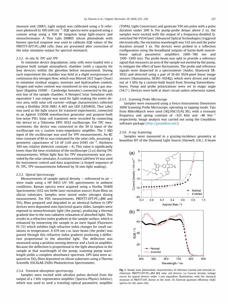
Fig. 1. Steady state photovoltaic characteristics of reference normal and inverted ar-chitecture PBDTTT-EFT:PC71BM BHJ solar cell devices. (a) Current densityevoltagecurves for typical devices under 1-sun equivalent illumination, with the chemicalstructure of PBDTTT-EFT shown in the inset. (b) External quantum efficiency (EQE)spectra for the same cells.
A.J. Pearson et al. / Organic Electronics 30 (2016) 225e236 227
measure unit (SMU). Light output was calibrated using a Si refer-ence photocell to 100 mW cm�2. EQE spectra were acquired using acustom setup using a 100 W tungsten lamp light-source andmonochromator. A Thor Labs SMR05 silicon photodiode withknown spectral response was used to calibrate EQE values of thePBDTTT-EFT:PC71BM cells. Data are presented after correction ofthe solar simulator output for spectral mismatch.
2.3.2. In-situ IV, TPC and TPVTo minimise device degradation, solar cells were loaded into a
purpose built sample atmospheric chamber (with a capacity forfour devices) within the glovebox before measurement. Duringeach experiment the chamber was held at a slight overpressure ofcontinuous dry nitrogen flow, which was filtered (SGT Super Clean)to minimise residual oxygen, moisture and hydrocarbon content.Oxygen and water content was monitored in-situ using a gas ana-lyser (Rapidox 3100D e Cambridge Sensotec) connected to the gasexit line of the sample chamber. A Newport Solar Simulator withequivalent 1 sun output was used for light-soaking the entire de-vice area, with solar cell currentevoltage characteristics collectedusing a Keithley 2636 SMU. A 465 nm LED (LED465E, Thor Labs)was used as the light source for transient experiments, connectedto an Agilent 33500B wavefunction generator and purpose-builtlow-noise PSU. Solar cell transients were recorded by connectingthe device to a Tektronix DPO 3032 oscilloscope. For TPC mea-surements, the device was connected to the 50 U input of theoscilloscope via a custom trans-impedance amplifier. The 1 MUinput of the oscilloscope was used for TPV measurements. An RCtime constant of 80 ns was estimated for the solar cells, assuming ageometric capacitance of 1.6 nF (cell area 0.045 cm�2, thickness100 nm, relative dielectric constant ~ 4). This value is significantlylower than the time resolution of the oscilloscope (2 ms) during TPCmeasurements. White-light bias for TPV measurements was pro-vided by the solar simulator. A customwritten LabViewVI was usedfor instrument control and data acquisition (a looped sequence ofIV, TPC, TPV measurements followed by 10 min light soaking).
2.3.3. Optical SpectroscopyMeasurements of sample optical density e referenced to air e
were made using a HP 8453 UVeVIS spectrometer in ambientconditions. Raman spectra were acquired using a Horiba T6400Spectrometer (632 nm HeNe laser excitation source) from films onsilicon substrates. Samples were stored under nitrogen duringmeasurement. For PDS measurements, PBDTTT-EFT:PC71BM andTiO2 films prepared and degraded in an identical fashion to OPVdevices were deposited onto Spectrosil quartz slides. Samples wereexposed to monochromatic light (the pump), producing a thermalgradient due to the non-radiative relaxation of absorbed light. Thisresults in a refractive index gradient at the sample surface, which isenhanced by immersing the sample in an inert liquid (FluorinertFC-72) which exhibits high refractive index changes for small var-iations in temperature. A 670 nm c.w. laser beam (the probe) waspassed through this refractive index gradient producing a deflec-tion proportional to the absorbed light. The deflection wasmeasured using a position sensing detector and a lock-in amplifier.Because the deflection is proportional to the light absorption in thesample at that wavelength of the pump, scanning pump wave-length yields a complete absorbance spectrum. UPS data were ac-quired on TiO2 films deposited on silicon substrates using a ThermoScientific ESCALAB 250Xi Photoelectron Spectrometer.
2.3.4. Transient absorption spectroscopySamples were excited with ultrafast pulses derived from the
output of a 1 kHz regenerative amplifier (Spectra-Physics Solstice),which was used to seed a traveling optical parametric amplifier
(TOPAS, Light Conversion) and generate 550 nm pulse with a pulseduration under 200 fs. For pump-probe delays above 2 ns, thesamples were excited with the output of a frequency-doubled Q-switched Nd-YVO4 laser (Advanced Optical Technologies) triggeredelectronically; the excitationwavelength was 532 nm and the pulseduration around 1 ns. The devices were probed in a reflectionconfiguration using the broadband outputs of home-built noncol-linear optical parametric amplifiers (600e780 nm and1100e1200 nm). The probe beam was split to provide a referencesignal that measures an area of the sample not excited by the pump,to mitigate the effect of laser fluctuations. The probe and referencesignals were dispersed in a spectrometer (Andor, Shamrock SR-303i) and detected using a pair of 16-bit 1024-pixel linear imagesensors (Hamamatsu, S8381-1024Q), which were driven and readout at 1 kHz by a custom-built board from Stresing Entwickluns-buero. Pump and probe polarizations were set to magic angle(54.7�). Devices were held at short circuit unless otherwise stated.
2.3.5. Scanning Probe MicroscopySamples were measured using a Veeco Instruments Dimension
3000 Scanning Probe Microscope, operating in tapping mode. Tipsfrom MikroMasch were used (HQ:NSC15/AL BS), with a resonantfrequency and spring constant of ~325 KHz and ~40 Nm�1
respectively. Image analysis was carried out using the Gwyddionsoftware package (http://gwyddion.net/).
2.3.6. X-ray ScatteringSamples were measured in a grazing-incidence geometry at
beamline I07 of the Diamond Light Source (Harwell, U.K.). A beam

A.J. Pearson et al. / Organic Electronics 30 (2016) 225e236228
energy of 10 keV was used with samples housed in a custom-builtchamber duringmeasurement. Samples were tilted at 0.16� into thepath of the incident X-rays. X-ray scatter was measured using aPilatus 2M detector, calibrated using silver behenate powder.Collected data was analysed using the DAWN software package(http://www.dawnsci.org/).
3. Results and discussion
3.1. Initial solar cell performance and lifetime data
In Fig. 1 we present the initial photovoltaic characteristics ofPBDTTT-EFT:PC71BM BHJ solar cell devices processed using chlo-robenzene solvent and DIO as a processing additive [32,33].
Reference solar cells were fabricated either in an inverted ar-chitecture, ITO/TiO2/PBDTTT-EFT:PC71BM/MoOx/Ag, or a normalarchitecture, ITO/PEDOT:PSS/PBDTTT-EFT:PC71BM/Ca/Ag [32].Because DIO has a high boiling point and a relatively low vapourpressure, small volumes are expected to linger in the polymer:-fullerene blend thin film after casting at ambient temperatures.Residual solvent is already known as a source of instability in OPVs[35] and so to counter this specific effect, blend films were washedwith methanol after casting to minimise residual DIO content priorto thermal evaporation of the back electrode [36]. Efficient photo-voltaic behaviour is obtained for devices fabricated according tothis protocol, with inverted and normal architecture devicesreaching average efficiencies of 6.0 ± 0.5% (JSC ¼ �15.1 mA cm�2,VOC ¼ 0.79 V, FF ¼ 50%) and 7.3 ± 0.5% (JSC ¼ �14.0 mA cm�2,VOC¼ 0.8 V, FF¼ 65%) respectively (the latter exhibiting identical FF
0 10 20 30 40 50 60 700.0
0.2
0.4
0.6
0.8
1.0
Met
ric /
Nor
mal
ised
Ageing time / hrs
FF VOC
JSC
PCE
0 10 20 30 40 50 60 700.0
0.2
0.4
0.6
0.8
1.0
PCE
/ Nor
mal
ised
Ageing time / hrs
Normal Inverted
(a) (b
(c) (d
Fig. 2. Performance under continuous simulated solar illumination of PBDTTT-EFT:PC71BMnormalised to their initial values. (b) Evolution of average performance metrics for invertedcells. Note that each quantity in (b) and (c) has been normalised to its initial value. (d) Compaextended dark storage, or after extended light soaking.
and VOC values to previous reports [32]). From Fig. 1 (b), it can beseen that the larger JSC of the inverted solar cell results from theenhanced spectral response in the UV and near-IR regions of thesolar spectrum.
The stability of the reference cells was evaluated over 70 hoursin an atmospheric chamber under continuous dry nitrogen flow,with typical oxygen and moisture levels of <5 ppm and <30 ppmrespectively. The chamber temperature e measured using an in-ternal Pt resistance thermometer placed next to the devices e didnot exceed 40 �C, this temperature being reached within 15 mi-nutes of the experiment commencing. An automated routine wasdeveloped to enable data collection after every 10 minutes of lightsoaking, with short (<30 s) intermediate periods of dark storageduring collection of TPC data. Solar cells were held at open circuitbetween currentevoltage scans. In Fig. 2, the evolution in solar cellperformance is presented, where individual metrics have beennormalised to their initial values. For both solar cell architectures asevere drop in PCE is observed, with the largest changes occurringwithin the first 24 hours. For inverted devices, the relative evolu-tion in individual metrics is presented in Fig. 2 (b), where it can beseen that the short-circuit current undergoes the largest overallreduction (80%) followed by the open circuit-voltage (40%).
For normal architecture devices the short circuit-current alsoundergoes the largest relative drop (see Fig. 2 (c)). Although the FFfor these solar cells undergoes a larger relative drop compared tothe inverted devices, the absolute values after stabilising arecomparable (40e45%). A control experiment was undertaken indark conditions to determine the extent to which the trace levels ofoxygen and water in the sample chamber atmosphere influence
-0.2 0.0 0.2 0.4 0.6 0.8 1.01E-5
1E-4
1E-3
0.01
0.1
1
10
Cur
rent
Den
sity
/ m
A cm
-2
Applied Bias / V
Initial 70 hrs (Dark storage) 70 hrs (Light soaked)
0 10 20 30 40 50 60 700.0
0.2
0.4
0.6
0.8
1.0
Met
ric /
Nor
mal
ised
Ageing time / hrs
FF VOC
JSC
PCE
)
)
reference cells. (a) Evolution of solar cell efficiency for normal and inverted devices,architecture cells. (c) Evolution of average performance metrics for normal architecturerison of dark currentevoltage behaviour for inverted architecture cells before and after

A.J. Pearson et al. / Organic Electronics 30 (2016) 225e236 229
device stability. The result of this experiment, presented in Fig. 2(d), does not show a significant change in diode characteristicsover a timescale similar to the original experiment (note that cur-rentevoltage scans were collected every 10 minutes as before). Incontrast, the dark IV behaviour of the light-soaked device issignificantly modified from its initial state. These results tentativelysuggest that burn-in in PBDTTT-EFT:PC71BM reference solar cells isdominated by light mediated processes.
3.2. In-situ transient characterisation of performance losses
To gain further insight into the loss of solar cell efficiency, weproceed to discuss the evolution in device performance as charac-terised through in-situ transient electrical measurements.
0 10 200.0
0.1
0.2
0.3
0.4
0.5
0.6
Cur
rent
at L
ED s
wtic
h of
f / m
A
Age
-0.2 -0.1 0.0 0.1 0.2 0.3 0.40.0
0.1
0.2
0.3
0.4
0.5
0.6
Cur
rent
/ m
A
Time / ms
Initial1 hr2 hrs4 hrs6 hrs 8 hrs10 hrs20 hrs30 hrs40 hrs50 hrs60 hrs70 hrs
(a) (
(c) (
1E-7 1E-6 1E-5 1E-4 1E-31E-4
1E-3
0.01
0.1
1
Cur
rent
nor
mal
ised
at
LED
sw
itch
off /
a.u
.
Time after LED switch off / s
Initial1 hr2 hrs4 hrs6 hrs 8 hrs10 hrs20 hrs30 hrs40 hrs50 hrs60 hrs70 hrs
(e)
Fig. 3. Evolution of the transient photocurrent (TPC) response from inverted architecture cepulse). (a) Absolute TPC response at distinct stages of the experiment, with data normalisedNote the different time axis presented in part (c). Throughout the entire experiment, the ipoints corresponding to a higher extracted charge than the trend arise from current fluctuaswitch off (quasi-steady-state) are compared with the current 10 ms after LED switch-on.
Specifically, the solar cell response to a 200 ms square-pulse opticalexcitation from a 465 nm LED was monitored either at short circuitfor TPC, or close to open circuit for TPV. The LED brightness (c.1 mW cm�2) was sufficiently low to ensure that the voltageperturbation during TPV measurements was less than 5% of VOC.The evolution in TPC characteristics for inverted architecture de-vices (which underwent the largest overall reduction in device ef-ficiency) is presented in Fig. 3. Individual TPC traces can be broadlydescribed according to three regimes of rapid (~ms) rise, adjustmentto a quasi-steady-state value, and rapid fall with a tail extending forup to several tens of ms. In general, fast components are oftenattributed to the transport of mobile charge carriers whereasslower components are attributed to charge trapping/detrappingprocesses [37].
30 40 50 60 70ing time / hrs
-0.10
-0.05
0.00
0.05
0.10 Current 10 m
s after LED sw
itch on - C
urrent at LED sw
itch off / mA
-0.2 -0.1 0.0 0.1 0.2 0.3 0.40.00
0.25
0.50
0.75
1.00
1.25
1.50
Cur
rent
nor
mal
ised
at L
ED s
witc
h of
f / a
.u.
Time / ms
Initial1 hr2 hrs4 hrs6 hrs 8 hrs10 hrs20 hrs30 hrs40 hrs50 hrs60 hrs70 hrs
b)
d)
0 10 20 30 40 50 60 701.50
1.75
2.00
2.25
2.50
2.75
3.00
Ext
ract
ed c
harg
e / n
C
Ageing time / hrs
lls during extended simulated solar illumination (t ¼ 0 ms defines the start of the LEDto the current at LED switch-off presented in (b) (entire data) and (c) (decay kinetics).ntegrated charge from each transient decay is plotted in (d), where intermittent datations 40 ms after LED switch-off. In part (e), changes in transient photocurrent at LED

Fig. 4. Evolution of the transient photocurrent (TPC) response from normal architecture cells during extended simulated solar illumination (t ¼ 0 ms defines the start of the LEDpulse). (a) Absolute TPC response at distinct stages of the experiment, with data normalised to the current at LED switch-off presented in (b) (entire data) and (c) (decay kinetics).Note the different time axis presented in part (c). Throughout the entire experiment, the integrated charge from each transient decay is plotted in (d) and (e), where part (e)highlights the initial rise in extracted charge during the first hour of ageing.
A.J. Pearson et al. / Organic Electronics 30 (2016) 225e236230
In Fig. 3 (a) it can be seen that the cell transient photocurrentundergoes a relative reduction with increasing exposure to simu-lated solar illumination, in agreement with the evolution in deviceshort-circuit current (Fig. 2 (b)). Furthermore, an overshoot inphotocurrent begins to emerge almost immediately following LEDswitch-on, relative to the values at 0.2 ms. In the regime shortlyafter LED switch-off (t > 0.2 ms), the tail in the TPC signal ismeasured to decay over progressively longer timescales during thecourse of the experiment i.e. with increasing degradation of thesolar cell. The relative significance of these features is highlighted inFig. 3 (b)e(c), where each TPC trace has been normalised to itscurrent value at LED switch-off (t ¼ 0.2 ms).
The overshoot in transient photocurrent measurements haspreviously been observed in bulk-heterojunctions of P3HT:PCBM[38], P3HT:F8BT [38] and polymer:nanocrystal photovoltaic devices[38,39], in addition to PCDTBT:PCBM BHJ devices under appliedbias [40]. In each case the overshoot was attributed to a build-up oftrapped charge, a process which modulates the internal electricfield in the device as it equilibrates with the transport of freecharges during steady-state illumination. Photocurrent loss maysubsequently occur via recombination of charge carriers, eitherthrough trap states or enhanced by space charge effects [40]. Abarrier to charge extraction [40-42] e that may be caused bymorphological changes in the active layer [42] e can also give rise

Fig. 5. Evolution in transient photovoltage (TPV) characteristics for reference solar cells as a function of 1 sun light soaking. Voltage transients after subtraction of VOC for (a)inverted devices and (b) normal devices. (b) VOC values overlaid with decay times t (right axis) for (c) inverted devices and (d) normal devices. Carrier lifetime as a function of VOC
for inverted (e) and normal (f) solar cells at different ageing times. To achieve different VOC values, the incident white light bias was varied using a series of neutral density filters.
A.J. Pearson et al. / Organic Electronics 30 (2016) 225e236 231
to this feature. Numerical simulations of P3HT:F8TBT BHJ OPVshave shown that the prominence of the current overshoot duringdevice illumination and the transient decay kinetics can be corre-lated with the density of trap states and the relative ratio of chargetrapping and de-trapping rates within the semiconductor blend[37]. Calculating these values however requires knowledge of boththe charge generation rate and the mobility of charge carrierswithin the solar cell, quantities that are not measured in-situ withour experimental setup.
Regarding the TPC decay kinetics in Fig. 3 (c), it can be seen thatdegradation increases the time for which current continues to flowfrom the solar cell after LED switch off. This observation is consis-tent with a relatively slow charge detrapping process taking place.We note that recent work on aged PCDTBT:PC71BM BHJ OPVs hasattributed an increased transient decay signal at relatively shorttimes (<20 ms after LED switch off) to trap states located at theelectrode interfaces of the solar cell [43]. Such trap states may alsoform in the system studied in this work, as we also observe asubstantial rise in signal at short times which modifies the globaldecay dynamics. Indeed, we find that beyond approximately10 hours into the experiment, a ‘kink’ emerges 30 ms after LEDswitch-off, which may suggest two distinct regimes of charge
detrapping [37]. The relative significance of bulk and electrodeinterface degradation behaviour for PBDTTT-EFT:PC71BM OPVsunder the conditions explored here is considered later on in ourdiscussion.
In Fig. 3 (d), the integrated current from each transient decay(t > 0.2 ms) is presented as a function of light soaking time. Here,the absolute extracted charge is found to increase at early lightsoaking times (up to approximately 20 hours) before decreasing.The initial increase is consistent with a greater population ofcharges becoming trapped within the solar cell during illumina-tion, before detrapping and undergoing subsequent extractionafter LED switch off. The measured decrease in extracted charge atlater times is potentially counterintuitive and we suggest that thisbehaviour reflects the development of a process that competeswith charge extraction. Specifically, following severe degradationit is possible that relatively deep traps exist within the solar cellfrom which charges are unlikely to escape from on the ms time-scale (i.e. commensurate with the TPC measurement period). Suchcharges would therefore not contribute to the extracted chargesignal which follows LED switch off. We note the close coincidencebetween the times at which the extracted charge is maximisedand when the burn-in phase is approximately complete (see Fig. 2

Fig. 6. (a) UVeVIS absorbance spectra for glass/ITO/TiO2/PBDTTT-EFT:PC71BM before and after 24 hours light soaking from the solar simulator. The absorbance of PBDTTT-EFT:PC71BM deposited on quartz/TiO2 and blank quartz substrates (as measured using PDS) are presented in (b) and (c) respectively, highlighting the differences in sub-bandgapfeatures that arise due to light soaking. The sub-bandgap absorbance of TiO2 on quartz is presented in (d). All films were degraded under nominally identical conditions to completedevices.
A.J. Pearson et al. / Organic Electronics 30 (2016) 225e236232
(b)) and when the dynamics of TPC decay are stabilised (see Fig. 3(c)), supporting the idea of kinetically distinct periods of devicedegradation over the course of the entire experiment. Lastly, inFig. 3 (e) we plot the TPC quasi-steady-state current against therelative prominence of the initial overshoot, here defined as thedifference in current at 0.01 ms and 0.2 ms. Because each quantityundergoes a similar evolution due to device burn-in (i.e. theemergence of the overshoot occurs simultaneously with a loss inquasi steady-state photocurrent), we hypothesise that the under-lying degradation mechanisms that give rise to these features areclosely linked.
The evolution in TPC dynamics for the normal architecture solarcells during ageing is presented in Fig. 4. In qualitative agreementwith the data presented in Fig. 3, it can be seen that light inducedburn-in also leads to an overall reduction in device photocurrent onthe ms timescale. This process does not result in the formation of an‘overshoot’ shortly after LED switch on, and we suggest that thisdifference partly explains why the inverted cells undergo a largeroverall reduction in photocurrent with ageing. Instead the loss inphotocurrent is correlated with a slower approach to a quasi stead-state value (c.f. normalised data in Fig. 4 (b)). Such behaviour can berationalised by a faster rate of charge trapping and/or a slower rateof charge detrapping [37], both of which will act to limit theextraction of charge carriers. Concerning the photocurrent decaydynamics (Fig. 4 parts (c)-(e)), we find that the extracted chargereaches a maximum within the first hour of ageing, beforedecreasing and stabilising after 20 hours.
We now consider the dynamics of both solar cells at VOC. Here,in-situ TPV was performed under 1-sun equivalent white light bias
to characterise the charge carrier recombination kinetics at distinctpoints in the degradation process. These results are presented inFig. 5. In parts (a) and (b), quasi-steady-state VOC values have beensubtracted from individual traces for ease of comparison.
From Fig. 5 (a)e(b) it can be seen that cell degradation resultsin an increase in charge carrier lifetime time under constantillumination (1 sun equivalent) conditions. Each TPV decay isapproximately linear when plotted on a log-linear scale, sug-gesting that charge carrier recombination is dominated by asingle mechanism in this regime [38]. To quantify the decay ki-netics we extract a time constant t by fitting each trace using asingle exponential of the form dV ¼ A exp(�t/t). Values for t areplotted as a function of light soaking time in Fig. 5 (c)e(d)alongside quasi-steady-state VOC values. Because t increases inline with a reduction in VOC over the course of the experiment,from approximately 1 mse12 ms for each architecture, it ispossible that the charge density n within the solar cell has beenreduced [44e46]. Although our setup does not permit the directmeasurement of n within a solar cell at VOC (e.g. by following themethod of charge extraction as described by Shuttle et al. [46]),TPV measurements as a function of white-light bias indicate thatat approximately constant VOC faster recombination dynamicsoccur in the degraded devices relative to their initial states (Fig. 5(e)e(f)). This result is consistent with the degraded devicesexhibiting poor microstructure and/or material energetics forphotocurrent generation [43,47] (c.f. Figs. 3e4 and the relateddiscussion on photocurrent loss), assuming that VOC remains areliable proxy for charge density throughout the conditionsexplored here.

Fig. 7. Transient absorption behaviour of inverted PBDTTT-EFT:PC71BM solar cell de-vices before and after 24 hours light soaking. (a) Normalised ultrafast dynamics oftransient absorption averaged between 1160 and 1180 nm, attributed to the polaronband on PBDTTT-EFT. (b) Normalised long-time dynamics of the polaron band. (c)Normalised long-time dynamics of the PBDTTT-EFT ground state bleach at750e780 nm.
A.J. Pearson et al. / Organic Electronics 30 (2016) 225e236 233
3.3. Ex-situ structural and optical characterisation of degradedPBDTTT-EFT:PC71BM solar cells
To test our hypothesis, we employ a range of techniques toidentify the underlying mechanisms that cause the observedreduction in PBDTTT-EFT:PC71BM reference cell PCE. Specifically,UVeVIS spectroscopy, photothermal deflection spectroscopy (PDS),transient absorption spectroscopy (TAS) were employed ex-situ tocharacterise the cumulative effects of the burn-in phase (approxi-mately 24 hours). These measurements are complemented byRaman spectroscopy, atomic force microscopy (AFM) and X-rayscattering measurements on the PBDTTT-EFT:PC71BM layer and UVphotoelectron spectroscopy (UPS) measurements; the latter usedfor characterising the cathode interface layer for the inverted de-vices (TiO2).
In Fig. 6, the absorbance of PBDTTT-EFT:PC71BM blend films ispresented before and after 24 hours simulated solar illumination.As shown in Fig. 6 (a), the shape of the PBDTTT-EFT:PC71BM ab-sorption spectrum remains broadly similar after light soaking. Asmall (~2 nm) blue-shift in the blend absorption peak initiallylocated at 712 nm is determined, as well as photobleaching (onaverage 6% between 380 and 800 nm). The magnitude of thephotobleach does not in itself account for the loss in JSC (c. 70% dropafter 24 hours), motivating further investigation [48]. Comple-mentary measurements of PBDTTT-EFT:PC71BM and TiO2 absor-bance were carried out using PDS to characterise sub-bandgapfeatures that cannot be resolved in a standard UVeVIS experiment.These results, shown in Fig. 6 (b) e (d), confirm that PBDTTT-EFT:PC71BM undergoes photobleaching, this process being appar-ently independent of the presence of TiO2 (c.f. parts (b) and (c)).Note that the data in Fig. 6 (b) provide some explanation for the lossin photocurrent of the normal architecture solar cells, as presentedearlier in Figs. 2 (c) and 4. PBDTTT-EFT:PC71BM undergoes a loss inabsorbance at all energies measured, in contrast to aged films ofPCDTBT:PCBM where light soaking was observed to increase sub-bandgap absorbance [13]. For TiO2 (Eg ~ 3.54 eV e see SupportingInformation Fig. S1) an average increase of 7% in sub bandgapabsorbance between 1.8 and 3.2 eV is determined (Fig. 6 (d)).Complementary UPS measurements (Supporting InformationFig. S2), do not evidence changes in the work function and valenceband positions of the metal oxide, although the signal intensity atthe secondary electron cut-off (binding energy ¼ 17.6 eV) isreduced. The PDS data suggest that the formation of sub-bandgapstates in TiO2 may well reflect a small increase in trap density,hindering the extraction of electrons through this layer in a com-plete solar cell device [49]. To summarise, we interpret our steady-state absorption measurements as an indication that light soakingdegrades both the PBDTTT-EFT:PC71BM layer and, to a lesser extent,the TiO2 cathode interface layer.
Finally, we discuss the differences in solar cell absorptioncharacteristics using TAS over timescales ranging from sub-ps to0.1 ms, where measurements in the sub-ns regime provide insightinto the dynamics of ultrafast charge generation and recombina-tion. Results are presented in Fig. 7. Measurements were conductedon devices held at short circuit using an excitation fluence of1 mJ cm�2, to minimise non-linear effects that are unlikely to ariseunder standard solar illumination conditions.
From Fig. 7 (a), it can be seen that the ultrafast dynamics of thetransient absorption feature at ~ 1170 nm e attributed to the holepolaron on PBDTTT-EFTe do not change as a result of light soaking.Specifically, both traces include an ultrafast rise that is attributed tofree charge generation at a donoreacceptor interface within thetime resolution of the setup (~200 fs). The slower component isattributed to free charge generation assisted by the diffusion ofphotogenerated excitons. The measurements therefore provide an
indirect but sensitive probe of the PBDTTT-EFT:PC71BM BHJ nano-structure. Because no changes are observed in the ultrafast TA ki-netics due to ageing, we conclude that light soaking for 24 hours at40 �C does not drive significant morphological changes in thePBDTTT-EFT:PC71BM blend (e.g. a coarsening phase separation be-tween electron donor and acceptor material that would otherwisemodify the balance of ultrafast and diffusion-assisted charge gen-eration). This is supported by AFM and X-ray scattering measure-ments that do not evidence changes in film structure at lengthscales above a few nm, as shown in Fig. 8. Specifically, the relative

Fig. 8. Comparison of PBDTTT-EFT:PC71BM blend nanostructures before and after 24 hours of light soaking, as measured via tapping-mode scanning probe microscopy and grazing-incidence wide-angle X-scattering (GIWAXS). Parts (a) and (b) show the topography for fresh and light-soaked samples respectively, whilst parts (c) and (d) show the correspondingphase maps. RMS roughness for each surface was <2 nm. GIWAXS measurements (e) indicate that ageing under solar illumination induces a shift of þ0.002 Å�1 in the diffractionpeak initially located at 0.317 Å�1, and a shift of �0.05 Å�1 in the diffraction peak initially located at 1.36 Å�1. These peaks are attributed to diffraction of X-rays between adjacentlamella of PBDTTT-EFT chains and adjacent PC71BM molecules respectively.
A.J. Pearson et al. / Organic Electronics 30 (2016) 225e236234
change in molecular packing between PBDTTT-EFT lamella oradjacent PC71BM molecules is less than 1%. Similarly, the size ofpolymer- and fullerene-rich domains within the blend thin filmalso remains stable; a Scherrer analysis of peak widths suggests anapproximate domain size of 7.2 nm and 2.3 nm for PBDTTT-EFT andPC71BM respectively, which changes to 7.0 nm and 2.4 nm after24 hours illumination.
We proceed to discuss the TAS data over the ns e ms timescale,presented in Fig. 7 (b)e(c). Here, the relatively long-time polaronkinetics (Fig. 7 (b)) show that the decay of this signal is unaffectedby light soaking. In contrast, changes are observed in the PBDTTT-EFT ground state bleach (GSB) dynamics in the ns e ms timerange (Fig. 7 (c)). Specifically, the GSB in the degraded device re-laxes over a relatively longer timescale than in the fresh device,with the fresh device exhibiting almost identical polaron and GSBdecay kinetics. In the presence of white light background
illumination (see Supporting Information Fig. S4), GSB relaxation ismodified further, with a full decay requiring tens of ms. The GSBdynamics of fresh devices are not affected by the presence ofbackground illumination, or by placing the device at open-circuitconditions. It is possible that the longer GSB decay time in thedegraded device occurs due to relaxation by additional excited statespecies (deeply trapped charges or triplet states) that do notcontribute to the solar cell photocurrent. We hypothesise that themechanism by which these additional states form is associatedwith the partial loss of chromophores that results from photo-bleaching of the PBDTTT-EFT:PC71BM blend layer (see Fig. 6).Although our work to identify these additional excited state speciesis ongoing, alongside experiments to confirm the exact chemicalmodifications in PBDTTT-EFT:PC71BM that result in this effect,preliminary measurements using resonance Raman spectroscopymeasurements do not evidence significant changes in the Raman
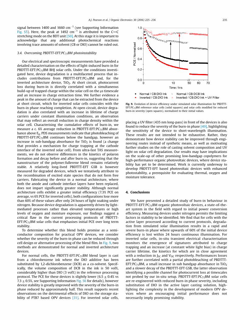
Fig. 9. Evolution of device efficiency under simulated solar illumination for PBDTTT-EFT:PC71BM reference solar cells (solid squares) and solar cells modified for reducedburn-in severity (open squares), normalised to their initial values.
A.J. Pearson et al. / Organic Electronics 30 (2016) 225e236 235
signal between 1400 and 1660 cm�1 (see Supporting InformationFig. S5). Here, the peak at 1492 cm�1 is attributed to the C]Cstretchingmode on the BDT unit [50]. At this stage it is important toacknowledge that any additional photochemical reactionsinvolving trace amounts of solvent (CB or DIO) cannot be ruled out.
3.4. Overcoming PBDTTT-EFT:PC71BM photoinstability
Our electrical and spectroscopic measurements have provided adetailed characterisation on the effects of light-induced burn-in forPBDTTT-EFT:PC71BM BHJ solar cells. Under the conditions investi-gated here, device degradation is a multifaceted process that in-cludes contributions from PBDTTT-EFT:PC71BM and, for theinverted architecture device, TiO2. At short circuit, photocurrentloss during burn-in is directly correlated with a simultaneousbuild-up of trapped charge within the solar cell on the ms timescaleand an increase in charge extraction time. We further evidence apeak in the amount of charge that can be extracted from the deviceat short circuit, which for inverted solar cells coincides with theburn-in phase reaching completion. At open circuit, device degra-dation is also correlated with an increase in lifetime of chargecarriers under constant illumination conditions, an observationthat may reflect an overall reduction in charge density within thesolar cell. Characterising the cumulative effects of burn-in, wemeasure a c. 6% average reduction in PBDTTT-EFT:PC71BM absor-bance above Eg. PDS measurements indicate that photobleaching ofPBDTTT-EFT:PC71BM continues below the bandgap, however anincrease in sub-bandgap absorbance for TiO2 is found (a changethat provides a mechanism for charge trapping at the cathodeinterface of the inverted solar cell). From ultra-fast TAS measure-ments, we do not observe differences in the kinetics of polaronformation and decay before and after burn-in, suggesting that thenanostructure of the polymer:fullerene blend remains relativelystable. A relatively long-lived PBDTTT-EFT GSB is howevermeasured for degraded devices, which we tentatively attribute tothe recombination of excited state species that do not form freecarriers. Fabricating the device in a normal architecture, whereboth the anode and cathode interface layers have been replaced,does not impart significantly greater stability. Although normalarchitecture cells exhibit a greater initial efficiency (7.3% PCE onaverage, vs 6% PCE for inverted cells), both configurations lose morethan 60% of these values after only 24 hours of light soaking undernitrogen. Because device degradation is apparently driven by light-mediated processes rather than elevated temperatures or highlevels of oxygen and moisture exposure, our findings suggest acritical flaw in the current processing protocols of PBDTTT-EFT:PC71BM solar cells that emphasises initial PCE over long termstability.
To determine whether this blend holds promise as a semi-conductor composition for practical OPV devices, we considerwhether the severity of the burn-in phase can be reduced throughcell design or alternative processing of the blend film. In Fig. 9, twomethods are demonstrated for normal and inverted architecturedevices.
For normal cells, the PBDTTT-EFT:PC71BM blend layer is castfrom a chlorobenzene ink where the DIO additive has beensubstituted by 1,2-dichlorobenzene (DCB) as a co-solvent. Specif-ically, the volume composition of DCB in the ink is 50 vol%,considerably higher than DIO (3 vol%) in the reference processingprotocol. The PCE for these devices is slightly lower (6.5 ± 0.4% vs7.3 ± 0.5%, see Supporting Information Fig. S6 for details), howeverdevice stability is greatly improved with the severity of the burn-inphase reduced by approximately half. This result supports recentobservations on the detrimental effects of DIO on the storage sta-bility of PTB7 based OPV devices [31]. For inverted solar cells,
placing a UV filter (435 nm long-pass) in front of the devices is alsofound to reduce the severity of the burn-in phase [49], highlightingthe sensitivity of the device to short-wavelength illumination.These results are not intended to be exhaustive. Rather, theydemonstrate how device stability can be improved through engi-neering routes instead of synthetic means, as well as motivatingfurther studies on the role of casting solvent composition and UVlight on solar cell degradation. Our results may have implicationson the scale-up of other promising low-bandgap copolymers forhigh-performance organic photovoltaic devices, where device sta-bility has yet to be determined. Work is currently underway todevelop PBDTTT-EFT based photovoltaic devices with enhancedphotostability, a prerequisite for evaluating thermal, oxygen andmoisture tolerance.
4. Conclusions
We have presented a detailed study of burn-in behaviour inPBDTTT-EFT:PC71BM organic photovoltaic devices, a state-of-the-art system in the field with regard to initial power conversionefficiency. Measuring devices under nitrogen permits the limitingfactors in stability to be identified. We find that for cells with theactive layer processed according to current protocols, degrada-tion from simulated solar illumination results in a rapid andsevere burn-in phase where upwards of 60% of the initial deviceefficiency is lost within 24 hours continuous illumination. Forinverted solar cells, in-situ transient electrical characterisationmonitors the emergence of signatures attributed to chargetrapping and an increase (at constant white light bias) in chargecarrier lifetime, the kinetics for which are in close agreementwith a reduction in JSC and VOC respectively. Performances lossesare further correlated with a partial photobleaching of PBDTTT-EFT:PC71BM, a small increase in sub bandgap absorbance in TiO2and a slower decay of the PBDTTT-EFT GSB, the latter observationidentifying a possible channel for photocurrent loss at timescalesnot probed by our in-situ setup. PBDTTT-EFT:PC71BM solar cellsare re-engineered with reduced burn-in phase severity, includingsubstitution of DIO in the active layer casting solution, high-lighting the complexity in the development of modern OPV de-vices where an encouraging initial performance does notnecessarily imply promising stability.

A.J. Pearson et al. / Organic Electronics 30 (2016) 225e236236
Acknowledgements
The authors would like to thank SABIC for partially funding thisresearch. PEH, EC and NCG thank the EPSRC for funding through theSupergen Supersolar Consortium (EP/J017361/1). PEH also thanksCKIK for additional funding. KD thanks the Gates CambridgeScholarship fund. MAJ thanks Nyak Technology Ltd for PhD schol-arship funding. AJP thanks David Lidzey (University of Sheffield) foruse of a sample chamber for X-ray scattering measurements andAdam Brown (University of Cambridge) for UPS measurements.
Appendix A. Supplementary data
Supplementary data related to this article can be found at http://dx.doi.org/10.1016/j.orgel.2015.12.024.
The data underlying this publication are available at https://www.repository.cam.ac.uk/handle/1810/253106.
References
[1] G. Li, R. Zhu, Y. Yang, Nat. Phot. 6 (2012) 153e161.[2] Z.C. He, C.M. Zhong, S.J. Su, M. Xu, H.B. Wu, Y. Cao, Nat. Phot. 6 (2012)
591e595.[3] J.B. You, L.T. Dou, K. Yoshimura, T. Kato, K. Ohya, T. Moriarty, K. Emery,
C.C. Chen, J. Gao, G. Li, Y. Yang, Nat. Commun. 4 (2013) 1446.[4] M.A. Green, K. Emery, Y. Hishikawa, W.Warta, E.D. Dunlop, Prog. Photovolt. 22
(2014) 1e9.[5] T. Wang, A.J. Pearson, D.G. Lidzey, J. Mater. Chem. C 1 (2013) 7266e7293.[6] R.S. Kularatne, H.D. Magurudeniya, P. Sista, M.C. Biewer, M.C. Stefan, J. Polym.
Sci. Pol. Chem. 51 (2013) 743e768.[7] Z.G. Zhang, J.Z. Wang, J. Mater. Chem. 22 (2012) 4178e4187.[8] M. Jorgensen, K. Norrman, S.A. Gevorgyan, T. Tromholt, B. Andreasen,
F.C. Krebs, Adv. Mater 24 (2012) 580e612.[9] H.L. Yip, A.K.Y. Jen, Energy Environ. Sci. 5 (2012) 5994e6011.
[10] K. Norrman, M.V. Madsen, S.A. Gevorgyan, F.C. Krebs, J. Am. Chem. Soc. 132(2010) 16883e16892.
[11] M. Jorgensen, K. Norrman, F.C. Krebs, Sol. Energy Mat. Sol. C 92 (2008)686e714.
[12] A. Tournebize, A. Rivaton, J.L. Gardette, C. Lombard, B. Pepin-Donat,S. Beaupre, M. Leclerc, Adv. Energy. Mater 4 (2014) 1301530.
[13] C.H. Peters, I.T. Sachs-Quintana, W.R. Mateker, T. Heumueller, J. Rivnay,R. Noriega, Z.M. Beiley, E.T. Hoke, A. Salleo, M.D. McGehee, Adv. Mater. 24(2012) 663e668.
[14] J. Kong, S. Song, M. Yoo, G.Y. Lee, O. Kwon, J.K. Park, H. Back, G. Kim, S.H. Lee,H. Suh, K. Lee, Nat. Commun. 5 (2014) 5668.
[15] T.M. Clarke, C. Lungenschmied, J. Peet, N. Drolet, K. Sunahara, A. Furube,A.J. Mozer, Adv. Energy. Mater. 3 (2013) 1473e1483.
[16] C.H. Peters, I.T. Sachs-Quintana, J.P. Kastrop, S. Beaupre, M. Leclerc,M.D. McGehee, Adv. Energy. Mater 1 (2011) 491e494.
[17] A. Tournebize, P.O. Bussiere, P. Wong-Wah-Chung, S. Therias, A. Rivaton,J.L. Gardette, S. Beaupre, M. Leclerc, Adv. Energy. Mater. 3 (2013) 478e487.
[18] E. Bovill, N. Scarratt, J. Griffin, H. Yi, A. Iraqi, A.R. Buckley, J.W. Kingsley,D.G. Lidzey, Appl. Phys. Lett. (2015) 106.
[19] W.R. Mateker, I.T. Sachs-Quintana, G.F. Burkhard, R. Cheacharoen,M.D. McGehee, Chem. Mater. 27 (2015) 404e407.
[20] Z. Li, H.C. Wong, Z.G. Huang, H.L. Zhong, C.H. Tan, W.C. Tsoi, J.S. Kim,J.R. Durrant, J.T. Cabral, Nat. Commun. 4 (2013) 2227.
[21] H.C. Wong, Z. Li, C.H. Tan, H.L. Zhong, Z.G. Huang, H. Bronstein, I. McCulloch,J.T. Cabral, J.R. Durrant, ACS Nano 8 (2014) 1297e1308.
[22] F. Piersimoni, G. Degutis, S. Bertho, K. Vandewal, D. Spoltore, T. Vangerven,J. Drijkoningen, M.K. Van Bael, A. Hardy, J. D'Haen, W. Maes, D. Vanderzande,M. Nesladek, J. Manca, J. Polym. Sci. Pol. Phys. 51 (2013) 1209e1214.
[23] L.Y. Lu, L.P. Yu, Adv. Mater. 26 (2014) 4413e4430.[24] S.J. Lou, J.M. Szarko, T. Xu, L. Yu, T.J. Marks, L.X. Chen, J. Am. Chem. Soc. 133
(2011) 20661e20663.[25] F. Liu, W. Zhao, J.R. Tumbleston, C. Wang, Y. Gu, D. Wang, A.L. Briseno, H. Ade,
T.P. Russell, Adv. Energy. Mater. 4 (2014) 1301377.[26] G.J. Hedley, A.J. Ward, A. Alekseev, C.T. Howells, E.R. Martins, L.A. Serrano,
G. Cooke, A. Ruseckas, I.D.W. Samuel, Nat. Commun. 4 (2013) 2867.[27] H.C. Liao, C.C. Ho, C.Y. Chang, M.H. Jao, S.B. Darling, W.F. Su, Mater. Today 16
(2013) 326e336.[28] I.P. Murray, S.J. Lou, L.J. Cote, S. Loser, C.J. Kadleck, T. Xu, J.M. Szarko,
B.S. Rolczynski, J.E. Johns, J.X. Huang, L.P. Yu, L.X. Chen, T.J. Marks,M.C. Hersam, J. Phys. Chem. Lett. 2 (2011) 3006e3012.
[29] J.B. You, C.C. Chen, L.T. Dou, S. Murase, H.S. Duan, S.A. Hawks, T. Xu, H.J. Son,L.P. Yu, G. Li, Y. Yang, Adv. Mater. 24 (2012) 5267e5272.
[30] Y. Wu, W. Zhang, X. Li, C. Min, T. Jiu, Y. Zhu, N. Dai, J. Fang, ACS Appl. Mater.Interfaces 5 (2013) 10428e10432.
[31] W. Kim, J.K. Kim, E. Kim, T.K. Ahn, D.H. Wang, J.H. Park, J. Phys. Chem. C 119(2015) 5954e5961.
[32] S.Q. Zhang, L. Ye, W.C. Zhao, D.L. Liu, H.F. Yao, J.H. Hou, Macromolecules 47(2014) 4653e4659.
[33] L. Ye, S.Q. Zhang, W.C. Zhao, H.F. Yao, J.H. Hou, Chem. Mater. 26 (2014)3603e3605.
[34] http://www.1-material.com/wp-content/uploads/2013/12/1M_From-PTB7-to-PCE-10_Confidential.pdf
[35] L.L. Chang, H.W.A. Lademann, J.B. Bonekamp, K. Meerholz, A.J. Moule, Adv.Funct. Mater. 21 (2011) 1779e1787.
[36] L. Ye, Y. Jing, X. Guo, H. Sun, S.Q. Zhang, M.J. Zhang, L.J. Huo, J.H. Hou, J. Phys.Chem. C 117 (2013) 14920e14928.
[37] I. Hwang, C.R. McNeill, N.C. Greenham, J. Appl. Phys. 106 (2009) 094506.[38] Z. Li, F. Gao, N.C. Greenham, C.R. McNeill, Adv. Funct. Mater. 21 (2011)
1419e1431.[39] F. Gao, Z. Li, J.P. Wang, A. Rao, I.A. Howard, A. Abrusci, S. Massip, C.R. McNeill,
N.C. Greenham, ACS Nano 8 (2014) 3213e3221.[40] Z. Li, C.R. McNeill, J. Appl. Phys. 109 (2011) 074513.[42] B.J.T. de Villers, R.C.I. MacKenzie, J.J. Jasieniak, N.D. Treat, M.L. Chabinyc, Adv.
Energy. Mater. 4 (2014) 1301290.[43] T. Heumueller, W.R. Mateker, I.T. Sachs-Quintana, K. Vandewal, J.A. Bartelt,
T.M. Burke, T. Ameri, C.J. Brabec, M.D. McGehee, Energy Environ. Sci. 7 (2014)2974e2980.
[44] D. Credgington, J.R. Durrant, J. Phys. Chem. Lett. 3 (2012) 1465e1478.[45] D. Credgington, R. Hamilton, P. Atienzar, J. Nelson, J.R. Durrant, Adv. Funct.
Mater. 21 (2011) 2744e2753.[46] C.G. Shuttle, A. Maurano, R. Hamilton, B. O'Regan, J.C. de Mello, J.R. Durrant,
Appl. Phys. Lett. 93 (2008) 183501.[47] X.G. Guo, N.J. Zhou, S.J. Lou, J. Smith, D.B. Tice, J.W. Hennek, R.P. Ortiz,
J.T.L. Navarrete, S.Y. Li, J. Strzalka, L.X. Chen, R.P.H. Chang, A. Facchetti,T.J. Marks, Nat. Phot. 7 (2013) 825e833.
[48] F. Deschler, A. De Sio, E. von Hauff, P. Kutka, T. Sauermann, H.J. Egelhaaf,J. Hauch, E. Da Como, Adv. Funct. Mater. 22 (2012) 1461e1469.
[49] T. Leijtens, G.E. Eperon, S. Pathak, A. Abate, M.M. Lee, H.J. Snaith, Nat. Com-mun. 4 (2013) 2885.
[50] J. Razzell-Hollis, J. Wade, W.C. Tsoi, Y. Soon, J. Durrant, J.S. Kim, J. Mater. Chem.A 2 (2014) 20189e20195.