cross thz imaging - israel institutes of technologyworkshop.ee.technion.ac.il/upload/files/dan...
TRANSCRIPT

© 2013 IBM Corporation
Cross THz Imaging
Evgeny Shumakher, Dan Corcos, Noam Kaminsky, Danny Elad IBM Haifa Research Lab Thomas Morf, Bernhard Klein IBM Zurich Research Lab
IBM Research
© 2013 IBM Corporation
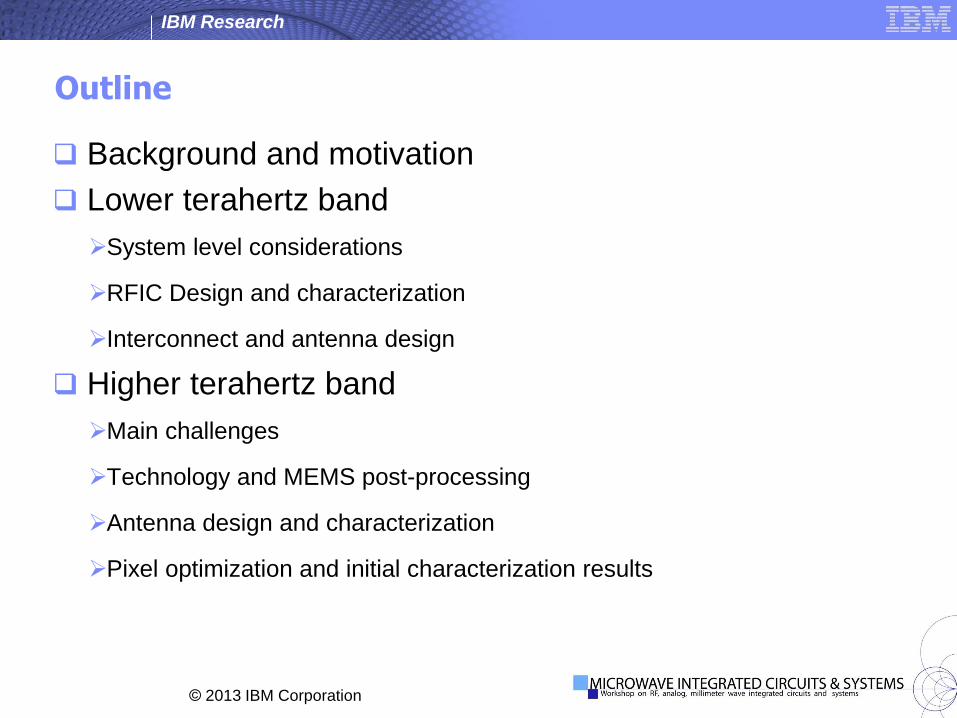
Outline
Background and motivation
Lower terahertz band
System level considerations
RFIC Design and characterization
Interconnect and antenna design
Higher terahertz band
Main challenges
Technology and MEMS post-processing
Antenna design and characterization
Pixel optimization and initial characterization results

IBM Research
© 2013 IBM Corporation
Perspective applications
Image by Millivision
Good weather photo
Good weather mm-wave image
Bad weather photo
Bad weather mm-wave image
Apparel fit Security screening Landing/Navigation aid
Image by Enea
Dental/Medical imaging

IBM Research
© 2013 IBM Corporation
State of the art
Cryogenically cooled systems
Very high cost and complexity
High sensitivity
Liquid Helium/Cryocompressor cooling
IPHT Jena
Uncooled passive systems
Compact, power efficient, safe
IBM Research
Active imaging system
Requires illumination with THz sources
High image contrast
Public concern about safety risks
L3 Comm.

IBM Research
© 2013 IBM Corporation
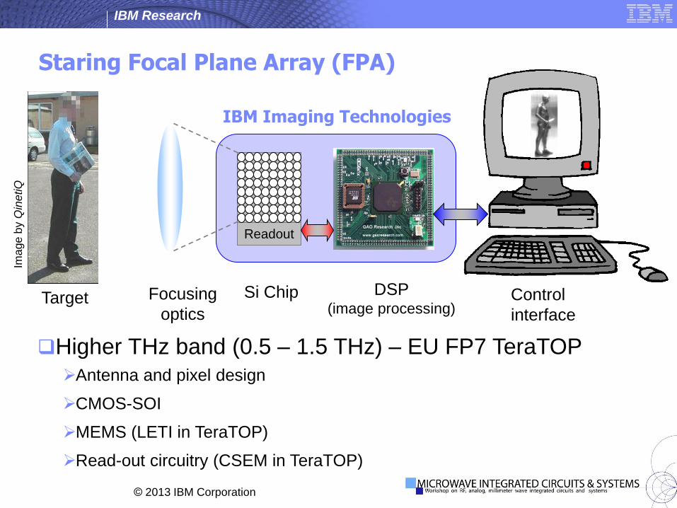
Focusing
optics
DSP (image processing)
Target Si Chip Control
interface
Ima
ge
by Q
ine
tiQ
Staring Focal Plane Array (FPA)
Readout
IBM Imaging Technologies
Lower THz band (0.1 – 0.3 THz)
Antenna and packaging
SiGe RFIC
Read-out circuitry
Image processing
IBM Research
© 2013 IBM Corporation
Higher THz band (0.5 – 1.5 THz) – EU FP7 TeraTOP
Antenna and pixel design
CMOS-SOI
MEMS (LETI in TeraTOP)
Read-out circuitry (CSEM in TeraTOP)
Focusing
optics
DSP (image processing)
Target Si Chip Control
interface
Ima
ge
by Q
ine
tiQ
Staring Focal Plane Array (FPA)
Readout
IBM Imaging Technologies

© 2013 IBM Corporation
Lower THz band
130 GHz Dicke radiometer in SiGe

IBM Research
© 2013 IBM Corporation
Dicke-radiometer based FPA
Primary
reflector
Secondary
reflector
D
Primary
reflector
Secondary
reflectorReceiver
complex
Close-up
LNA
ANT
on
PCKG
DSPD
OUTanlg
ROI
INRF
RX
DATA + CTRL
ANT
NS
SPI
Clo
se
-up

IBM Research
© 2013 IBM Corporation
Dicke-radiometer state of the art
Reference Year Technology Integration Frequency NETD
Voinigescu, U
Toronto
2012 0.13um SiGe
BiCMOS, STM
LNA+PD 160 – 170 GHz 0.35 K
Rebeiz, UC SD 2010 8HP, IBM DS+LNA+PD 84 – 99 GHz 0.83 K
Heydari, UC Irvine 2010 0.18um SiGe
BiCMOS, Jazz
DS+LNA+PD 70 – 96 GHz 0.4 K
Voinigescu, U
Toronto
2009 65 nm CMOS,
STM
DS+LNA+PD 81 – 93 GHz 0.55 K
LNA
ANT
on
PCKG
DSPD
OUTanlg
ROI
INRF
RX
DATA + CTRL
ANT
NS
SPI

IBM Research
© 2013 IBM Corporation
Specifications
Standard IBM 0.13um SiGe Technology fT/fMAX ~ 180/220 GHz
5 layer metallization
MiM capacitors available
Packaging losses < 3 dB Dicke-switch
< 3 dB insertion loss
> 15 dB on-off extinction ratio
LNA Gain of 25-30 dB
Bandwidth of 15 – 20 GHz
NF < 10 dB
Power detector NEP < 5 pW/Hz1/2
General design constraints 1. Consumed power
2. Allocated area
Silicon substrate
CPWG
Transmission line
GND
Side
shielding
Auxillary routing
MoM capacitors

IBM Research
© 2013 IBM Corporation
Dicke switch
RFIN
RFOUT
50
SE
S SE
SPDT topology
3 versions of Switching Element
designed
Single 120 um Triple-well NFET
Double 60 um Triple-well NFET
Triple 36 um NPN HBT
LNA
ANT
on
PCKG
DSPD
OUTanlg
ROI
INRF
RX
DATA + CTRL
ANT
NS
SPI

IBM Research
© 2013 IBM Corporation
Dicke switch
SPDT topology
3 versions of Switching Element
designed
Single 120 um Triple-well NFET
Double 60 um Triple-well NFET
Triple 36 um NPN HBT
350 um
LNA
ANT
on
PCKG
DSPD
OUTanlg
ROI
INRF
RX
DATA + CTRL
ANT
NS
SPI
IBM Research
© 2013 IBM Corporation
Dicke switch
80 90 100 110 120 130 140 150 160-25
-20
-15
-10
-5
0
Frequency [GHz]
|S21|
[dB
]
STW
DTW
HBT
ON
OFF
LNA
ANT
on
PCKG
DSPD
OUTanlg
ROI
INRF
RX
DATA + CTRL
ANT
NS
SPI

IBM Research
© 2013 IBM Corporation
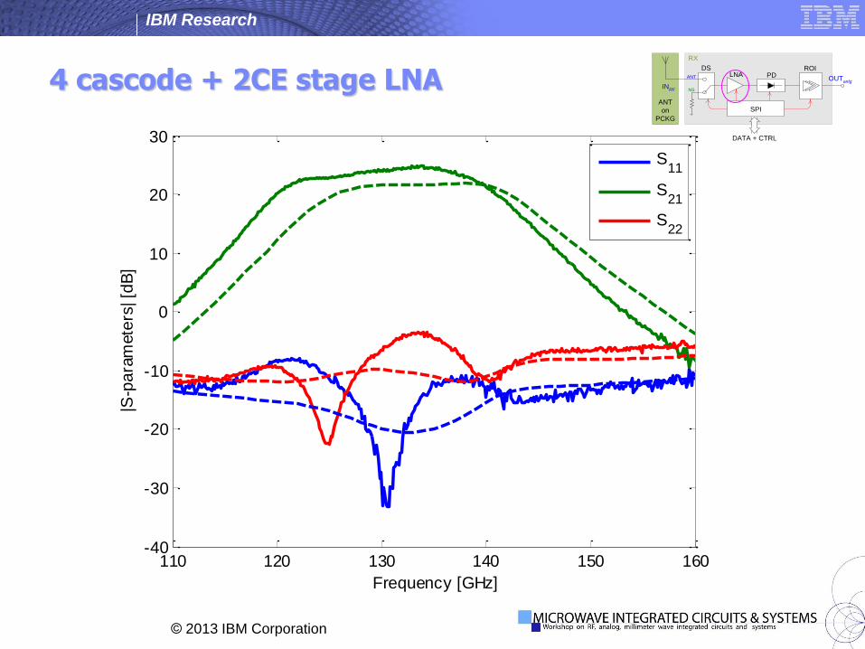
4 cascode + 2CE stage LNA
RF Match
RF C/M RF C/M RF C/M RF C/M
VCC
Vb12
Vb11
Vb21
Vb22
Vb31
Vb32
Vb41
Vb42
RF C/M
Vb51
Vb52
Current re-use
CE
LNA
ANT
on
PCKG
DSPD
OUTanlg
ROI
INRF
RX
DATA + CTRL
ANT
NS
SPI

IBM Research
© 2013 IBM Corporation
4 cascode + 2CE stage LNA LNA
ANT
on
PCKG
DSPD
OUTanlg
ROI
INRF
RX
DATA + CTRL
ANT
NS
SPI
400 um
IBM Research
© 2013 IBM Corporation
4 cascode + 2CE stage LNA
110 120 130 140 150 160-40
-30
-20
-10
0
10
20
30
Frequency [GHz]
|S-p
ara
mete
rs| [d
B]
S11
S21
S22
LNA
ANT
on
PCKG
DSPD
OUTanlg
ROI
INRF
RX
DATA + CTRL
ANT
NS
SPI

IBM Research
© 2013 IBM Corporation
Power detector
Vb
RF Trap
RF Match
RFIN
VCCVBB VCC
Vb
RF Trap
RF Match
VBB VCC
KQ Resistor
RFIN
Vb
120 um
LNA
ANT
on
PCKG
DSPD
OUTanlg
ROI
INRF
RX
DATA + CTRL
ANT
NS
SPI

IBM Research
© 2013 IBM Corporation
Power detector
10-7
10-6
10-5
10-4
103
104
105
Incident power [W]
Resp
osiv
ity [
V/W
]
meas
sim
103
104
105
10-8
10-7
Frequency [Hz]
VS
D [
V/
Hz]
HzpWNEP 5
LNA
ANT
on
PCKG
DSPD
OUTanlg
ROI
INRF
RX
DATA + CTRL
ANT
NS
SPI

IBM Research
© 2013 IBM Corporation
Package design
Flip-chip
Low loss ( < 1.5 dB)
Small space – a little bigger than chip size
Pads do not have to be only on the periphery
Easy to dissipate heat in our application
10.00 40.00 70.00 100.00 130.00 160.00Freq [GHz]
-1.75
-1.50
-1.25
-1.00
-0.75
-0.50
-0.25
0.00
dB
(S(C
PW
_p
ort
,ms
trip
))
Ansoft LLC gold_stud_matchS21 ANSOFT
Curve Info
dB(S(CPW_port,mstrip))Setup1 : Sw eep1L='-2mil'

IBM Research
© 2013 IBM Corporation
Antenna design
Per-pixel antenna
Wide-band horn antenna

IBM Research
© 2013 IBM Corporation
-5
-4.5
-4
-3.5
-3
-2.5
-2
-1.5
-1
-0.5
0
110 115 120 125 130 135 140
Frequency [GHz]
Ins
ert
ion
lo
ss
[d
B]
Simulation
Material A
Material B
Material C
Antenna design
Microstrip to waveguide
interconnect
Simple package design
Good results at 120GHz

© 2013 IBM Corporation
Upper THz band EU FP7 TeraTOP
Uncooled antenna-coupled MOSFET
bolometer in CMOS-SOI-MEMS

IBM Research
© 2013 IBM Corporation
The challenge of Passive THz detection
Detect radiation at 0.5 – 1.5 THz with NETD = 1 [K]
Very low frequencies compared to optical waves (like visible and infrared)
Spontaneous emission (in the THz range) is 1/1000 with respect to the IR
Still too high for solid-state electronics (perhaps in the future ?)
THz
Wavelength
Rad
iate
d p
ow
er
Body temperature
IR

IBM Research
© 2013 IBM Corporation
Goals
Sophisticated pixels are needed:
Broadband antennas – collect as much in-band signal as possible
Light-weight – low thermal time constant (required for real-time imaging)
Coupling to fast optics – overlap and spill-over efficiency through the band
High sensitivity – achieve very low noise and high responsivity
Narrow BW 500-580 GHz Broad BW 500-1000 GHz Original temperature map
Image simulations including detector NEP = 25 pW
Conflict
Virtual prototyping:

IBM Research
© 2013 IBM Corporation
IBM detector technology - Overview
On-chip planar antennas with 0.6 -1.4 THz bandwidth
MOSFET bolometer with large temperature responsivity
High thermal isolation achieved by MEMS and vacuum packaging (10-2 mbar)
Target Noise Equivalent Temp. Difference (NETD) < 1 K in real-time
Cloverleaf
antenna
Transistor
and termination
Legs
Example: suspended “cloverleaf” antenna
SEM
picture of
a MEMS
antenna
array
FPA cross-section
IBM Research
© 2013 IBM Corporation
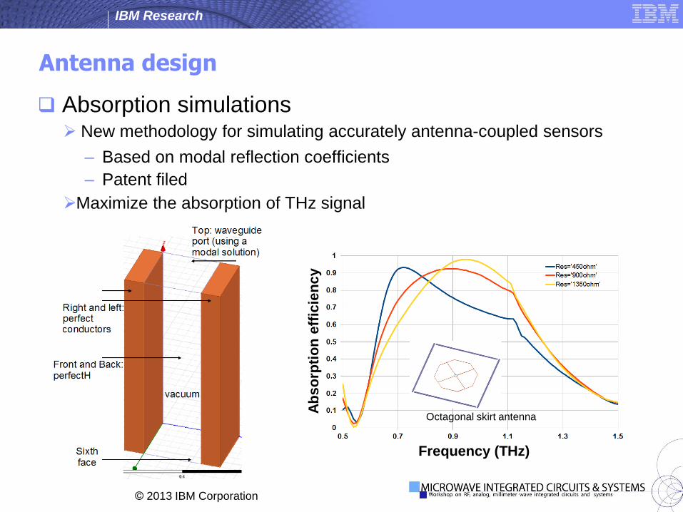
Antenna design
Absorption simulations New methodology for simulating accurately antenna-coupled sensors
– Based on modal reflection coefficients
– Patent filed
Maximize the absorption of THz signal
Ab
so
rpti
on
eff
icie
nc
y
Frequency (THz)
Octagonal skirt antenna

IBM Research
© 2013 IBM Corporation
Antenna design
Transmission simulations
Evaluate radiation pattern across the band
Cloverleaf antenna
0.6THz 1THz 1.4THz

IBM Research
© 2013 IBM Corporation
Technology
Standard IBM 0.18 μm CMOS-SOI process BOX thickness 1μm
4 metal layers as built-in masks
MEMS post-CMOS process Front side dry etch
Metal mask wet etch
Back side wet etch
b) RIE
c) Wet etch
a) CMOS Fab
d) DRIE

IBM Research
© 2013 IBM Corporation
MEMS post-processing in IBM Zurich facility
Fully released 13x9 array
High functional “survival rate”
The antennas are still planar
after release
Some holding arms are bent
upwards
This is fine as long as they
don’t touch

IBM Research
© 2013 IBM Corporation
MEMS post-processing

IBM Research
© 2013 IBM Corporation
MEMS post-processing
IBM Research
© 2013 IBM Corporation
Detector optimization involves best
MOSFET sizing and operating point to
yield
We aim to achieve the lowest NEP
Responsivity is increased by using large
currents, but so is noise
A noise reduction method was developed for
filtering the 1/f noise
We expect to achieve NEP≈13 pW with
ROIC bandwidth of 100 Hz
Detector optimization
NEP=13 pW
Legend
• Non-optimized sizing, ideal voltage ROIC
• Optimized sizing, ideal voltage ROIC
• Optimized sizing, ROIC with 1/f reduction

IBM Research
© 2013 IBM Corporation
Antenna characterization
Measurement of the radiation patterns in air at 0.65 THz
THz source based on chain of frequency multipliers
Pixels outside of Dewar for avoiding reflections on the walls
But results in lower responsivity
Test board
THz
source
Rotation stage
Measurement setup at Univ. of Wuppertal

IBM Research
© 2013 IBM Corporation
Antenna characterization
Measurement of the normalized responsivity at 0.65 THz
Several types of antenna were tested
Half-power beamwidth in good agreement with HFSS
Normalized radiation pattern of a
log-spiral antenna
The beams are broad by design (±40° typical)
for best coupling with fn<1 lenses
Current responsivity
(symbols = types of antennas)
Measurements match with the design.
Responsivity is 400x lower in air vs. vacuum

IBM Research
© 2013 IBM Corporation
1/f noise is dominant for bandwidths < 1kHz
Noise of un-processed devices fits BSIMSOI
model parameters from the PDK
2x increase in 1/f power due to plasma
induced damage (MEMS) ~1.4x in NEP
PSD of HV NFET vs. gate bias
Measurement setup
Noise simulations vs. measurements
Pixel Noise
DUT
1/f noise dominates the
total pixel noise
Measurement of pixel type “spiral3”
Excellent fit with simulation

IBM Research
© 2013 IBM Corporation
Summary – Lower band
Key components of a 130 GHz Dicke-radiometer
Realized in standard 0.12 μm SiGe process
Designed for incorporation into very large FPA
Dicke-switch (SPDT)
< 3 dB insertion loss
> 12 dB extinction ratio
LNA
4 cascode + 2 CE stage : > 24 dB gain in 20 GHz bandwidth
Noise figure characterization pending
PD
Demonstrated with NEP ≈ 5pW/Hz1/2
Packaging
Coupling losses < 3 dB

IBM Research
© 2013 IBM Corporation
Summary – Higher band
THz pixels based on antenna-coupled MOSFET
bolometers
IBM 0.18 μm CMOS-SOI process with MEMS post-processing
THz antennas
Several new antennas for exploring the bandwidth vs. speed tradeoff
Measured HPBW (±40° typical) matching with the design
MOSFET sensors
High thermal sensitivity with MOSFET bolometers and MEMS
Simulated sensor NEP=13 pW for ROIC bandwidth of 100 Hz
Responsivity
Initial measurements (1 mA/W in air) in good agreement with simulation in
corresponding conditions
Upcoming measurements in vacuum with blackbody source

IBM Research
© 2013 IBM Corporation
Acknowledgements
Dr. Eran Socher, Tel Aviv University
D-band measurement facility
IBM Tokyo Research Lab
D-band flip-chip interconnect mechanical and thermal design
Prof. Ullrich Pfeiffer, University of Wuppertal
THz antenna characterization
The European Union 7th Framework Program
TeraTOP Project