cryogenic operation of field programmable gate … · cryogenic operation of field programmable...
TRANSCRIPT
Cryogenic Operation of Field Programmable Gate Arrays
Douglas Sheldon1, Gary Burke1, Arby Argueta1, Alireza Bakshi2, Nazeeh Aranki1, Michael Sadigursky1
1Jet Propulsion Laboratory, 2B&A Engineering Systems
Jet Propulsion LaboratoryCalifornia Institute of Technology
© 2011 California Institute of Technology. All rights reserved.
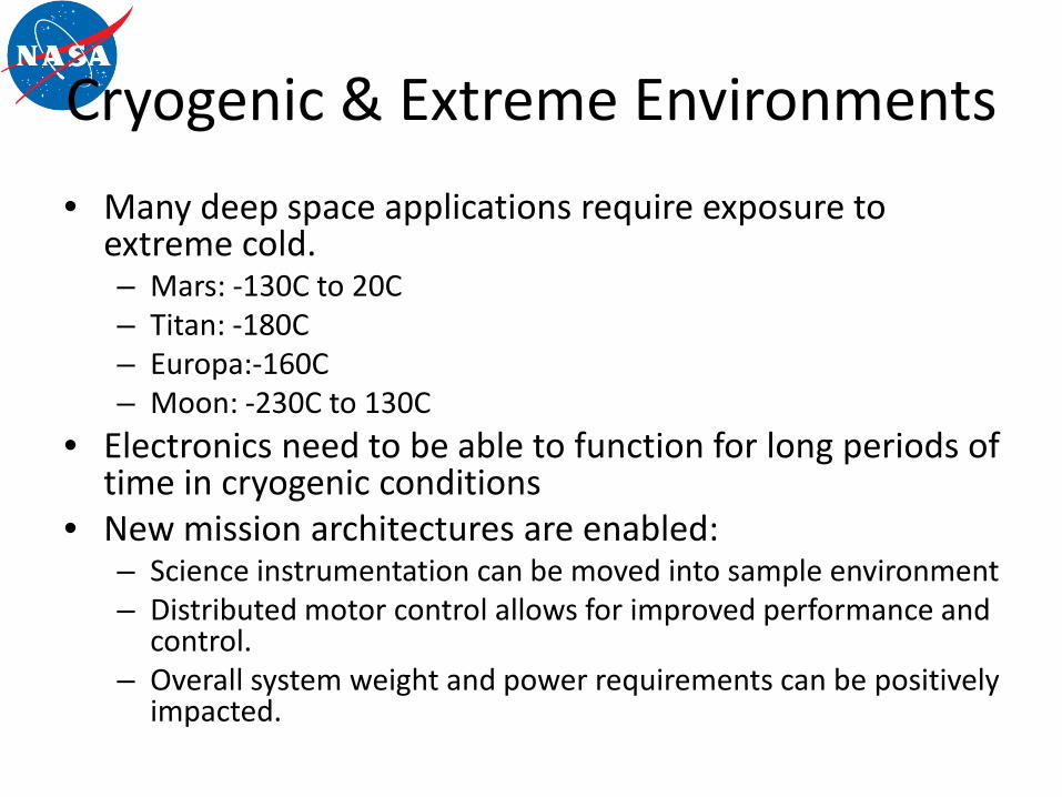
Cryogenic & Extreme Environments• Many deep space applications require exposure to
extreme cold.– Mars: -130C to 20C – Titan: -180C– Europa:-160C– Moon: -230C to 130C
• Electronics need to be able to function for long periods of time in cryogenic conditions
• New mission architectures are enabled:– Science instrumentation can be moved into sample environment– Distributed motor control allows for improved performance and
control.– Overall system weight and power requirements can be positively
impacted.
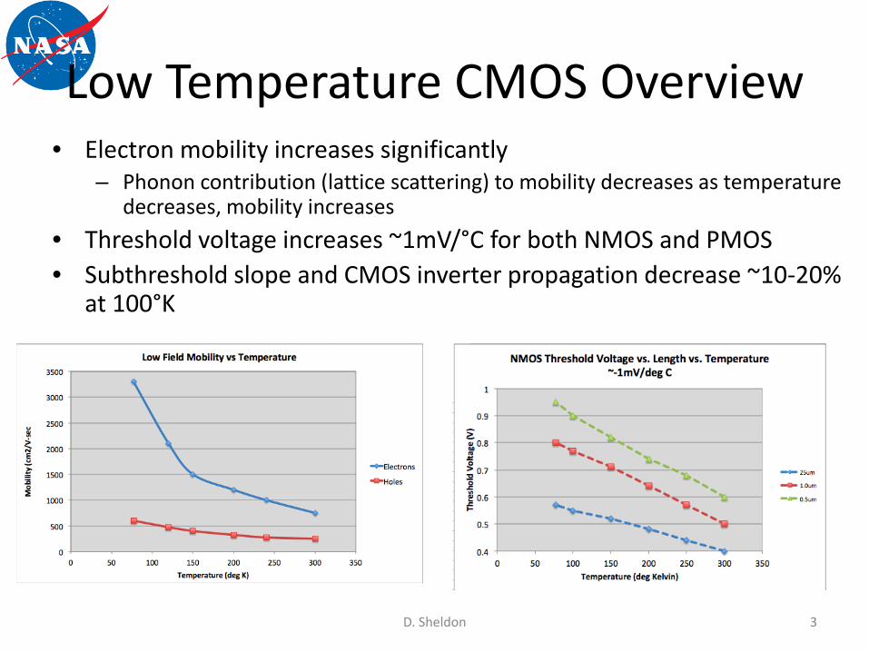
Low Temperature CMOS Overview• Electron mobility increases significantly
– Phonon contribution (lattice scattering) to mobility decreases as temperature decreases, mobility increases
• Threshold voltage increases ~1mV/°C for both NMOS and PMOS• Subthreshold slope and CMOS inverter propagation decrease ~10-20%
at 100°K
D. Sheldon 3
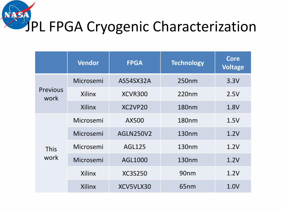
JPL FPGA Cryogenic Characterization
Vendor FPGA Technology Core Voltage
Previous work
Microsemi AS54SX32A 250nm 3.3V
Xilinx XCVR300 220nm 2.5V
Xilinx XC2VP20 180nm 1.8V
This work
Microsemi AX500 180nm 1.5V
Microsemi AGLN250V2 130nm 1.2V
Microsemi AGL125 130nm 1.2V
Microsemi AGL1000 130nm 1.2V
Xilinx XC3S250 90nm 1.2V
Xilinx XCV5VLX30 65nm 1.0V
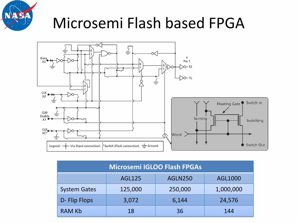
Microsemi Flash based FPGA
Microsemi IGLOO Flash FPGAsAGL125 AGLN250 AGL1000
System Gates 125,000 250,000 1,000,000
D- Flip Flops 3,072 6,144 24,576
RAM Kb 18 36 144
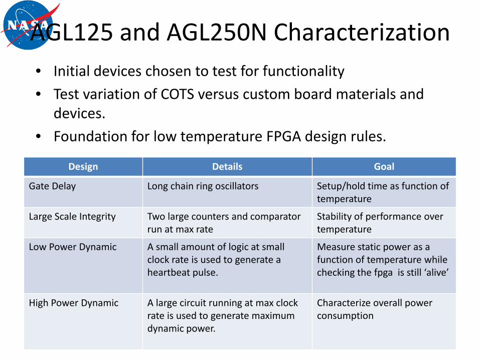
AGL125 and AGL250N Characterization• Initial devices chosen to test for functionality• Test variation of COTS versus custom board materials and
devices.• Foundation for low temperature FPGA design rules.
Design Details Goal
Gate Delay Long chain ring oscillators Setup/hold time as function of temperature
Large Scale Integrity Two large counters and comparator run at max rate
Stability of performance over temperature
Low Power Dynamic A small amount of logic at small clock rate is used to generate a heartbeat pulse.
Measure static power as a function of temperature while checking the fpga is still ‘alive’
High Power Dynamic A large circuit running at max clock rate is used to generate maximum dynamic power.
Characterize overall power consumption
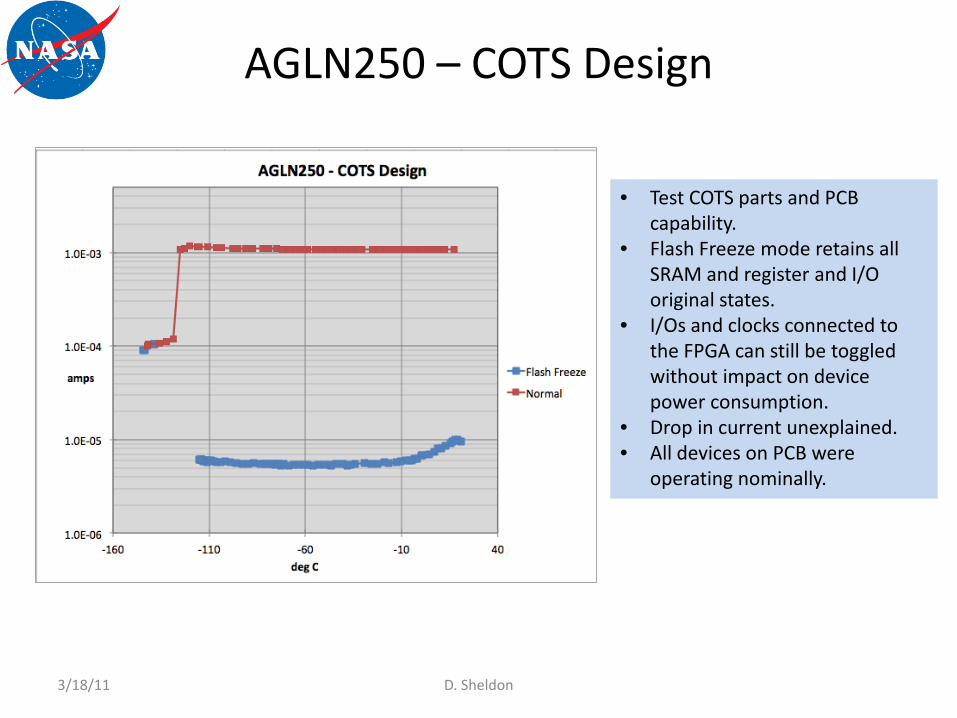
AGLN250 – COTS Design
D. Sheldon3/18/11
• Test COTS parts and PCB capability.
• Flash Freeze mode retains all SRAM and register and I/O original states.
• I/Os and clocks connected to the FPGA can still be toggled without impact on device power consumption.
• Drop in current unexplained.• All devices on PCB were
operating nominally.
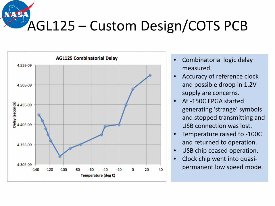
AGL125 – Custom Design/COTS PCB
• Combinatorial logic delay measured.
• Accuracy of reference clock and possible droop in 1.2V supply are concerns.
• At -150C FPGA started generating ‘strange’ symbols and stopped transmitting and USB connection was lost.
• Temperature raised to -100C and returned to operation.
• USB chip ceased operation.• Clock chip went into quasi-
permanent low speed mode.
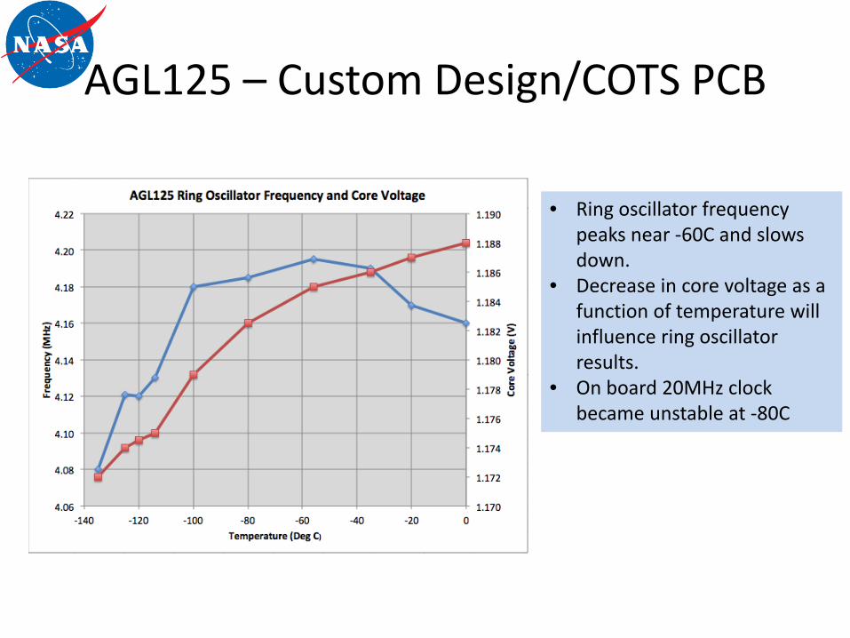
AGL125 – Custom Design/COTS PCB
• Ring oscillator frequency peaks near -60C and slows down.
• Decrease in core voltage as a function of temperature will influence ring oscillator results.
• On board 20MHz clock became unstable at -80C
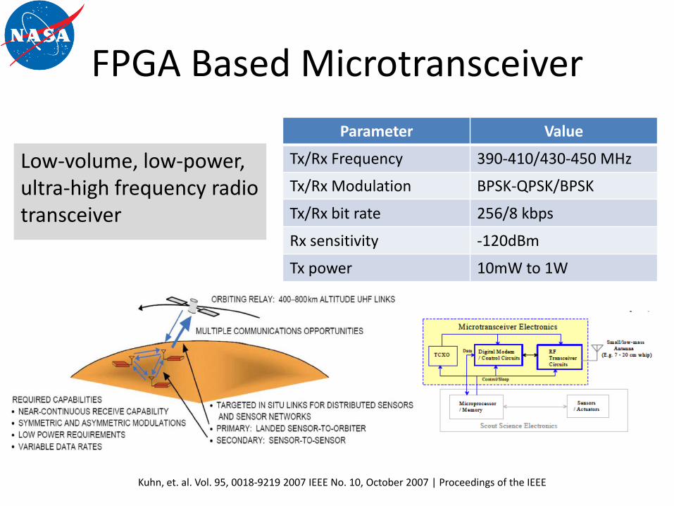
FPGA Based Microtransceiver
Low-volume, low-power, ultra-high frequency radio transceiver
Kuhn, et. al. Vol. 95, 0018-9219 2007 IEEE No. 10, October 2007 | Proceedings of the IEEE
Parameter Value
Tx/Rx Frequency 390-410/430-450 MHz
Tx/Rx Modulation BPSK-QPSK/BPSK
Tx/Rx bit rate 256/8 kbps
Rx sensitivity -120dBm
Tx power 10mW to 1W
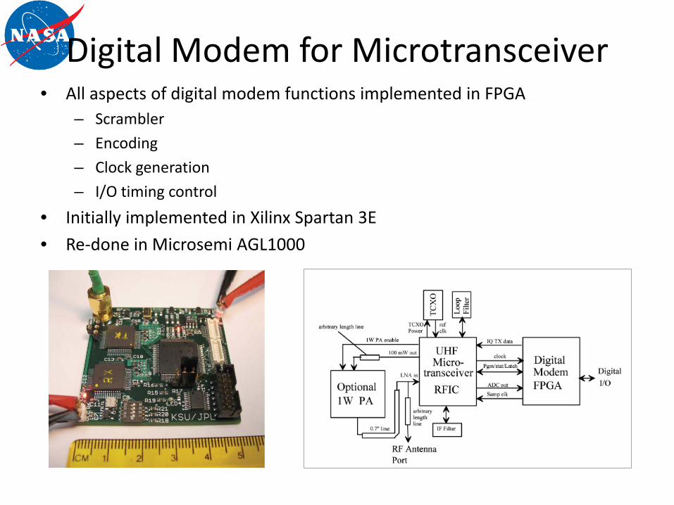
Digital Modem for Microtransceiver • All aspects of digital modem functions implemented in FPGA
– Scrambler– Encoding– Clock generation– I/O timing control
• Initially implemented in Xilinx Spartan 3E• Re-done in Microsemi AGL1000
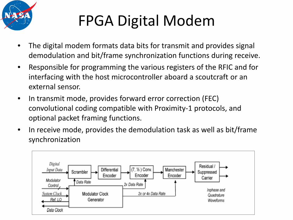
FPGA Digital Modem• The digital modem formats data bits for transmit and provides signal
demodulation and bit/frame synchronization functions during receive. • Responsible for programming the various registers of the RFIC and for
interfacing with the host microcontroller aboard a scoutcraft or an external sensor.
• In transmit mode, provides forward error correction (FEC) convolutional coding compatible with Proximity-1 protocols, and optional packet framing functions.
• In receive mode, provides the demodulation task as well as bit/frame synchronization
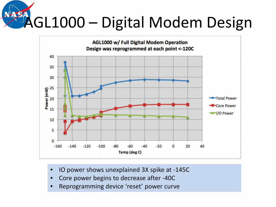
AGL1000 – Digital Modem Design
• IO power shows unexplained 3X spike at -145C• Core power begins to decrease after -40C• Reprogramming device ‘reset’ power curve
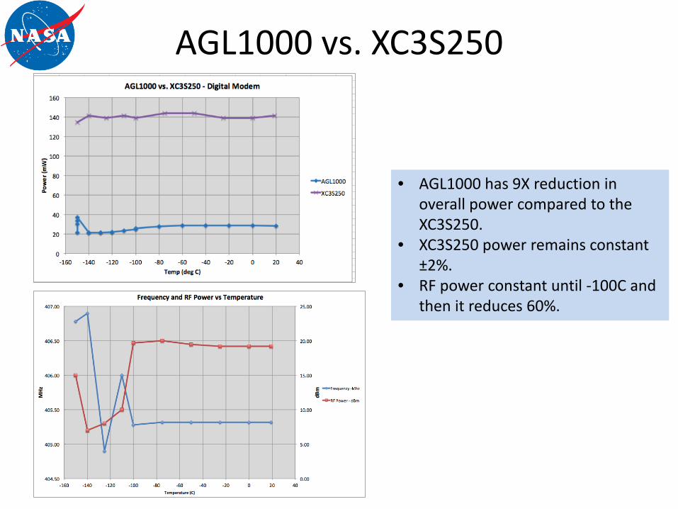
AGL1000 vs. XC3S250
• AGL1000 has 9X reduction in overall power compared to the XC3S250.
• XC3S250 power remains constant ±2%.
• RF power constant until -100C and then it reduces 60%.
AX500 Design
• AX500:– 500K gates/5.3K FF/73Kb Core RAM– No SEU enhanced CLK or TMR FF– PQ208 package
• Pulse Width Modulator circuit:– 5/10 KHz PWM resolver frequency controlled via test
instruments.– Using internal AX500 PLLs, 50 & 100 MHz clock
outputs are generated from the 100 MHz on the board oscillator
XC5VLX30 Design
• XC5VLX30:– 4.8K slices/30K Logic cells/19.2K FF/1.1Mb BRAM– 4 DCM/2 PLL– FF324 Package
• Stability and performance of:– Internal PLLs – Ring oscillator – Combinatorial logic circuits– Same PLL was used to both divide and multiply the master
on-board oscillator to generate the 50/150 MHz clocks.
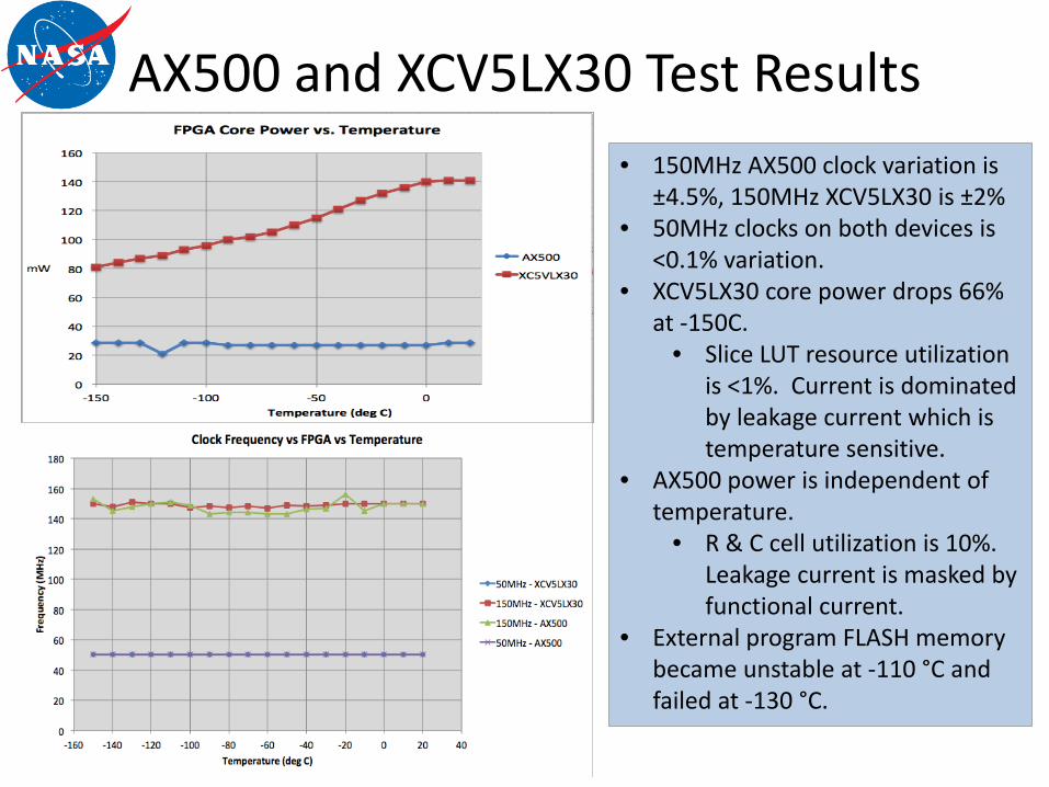
AX500 and XCV5LX30 Test Results• 150MHz AX500 clock variation is
±4.5%, 150MHz XCV5LX30 is ±2%• 50MHz clocks on both devices is
<0.1% variation.• XCV5LX30 core power drops 66%
at -150C.• Slice LUT resource utilization
is <1%. Current is dominated by leakage current which is temperature sensitive.
• AX500 power is independent of temperature.
• R & C cell utilization is 10%. Leakage current is masked by functional current.
• External program FLASH memory became unstable at -110 °C and failed at -130 °C.
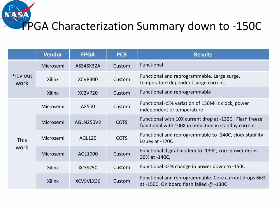
FPGA Characterization Summary down to -150C
Vendor FPGA PCB Results
Previous work
Microsemi AS54SX32A Custom Functional
Xilinx XCVR300 Custom Functional and reprogrammable. Large surge, temperature dependent surge current.
Xilinx XC2VP20 Custom Functional and reprogrammable
This work
Microsemi AX500 Custom Functional <5% variation of 150MHz clock, power independent of temperature
Microsemi AGLN250V2 COTS Functional with 10X current drop at -130C. Flash freeze functional with 100X in reduction in standby current.
Microsemi AGL125 COTS Functional and reprogrammable to -140C, clock stability issues at -120C
Microsemi AGL1000 Custom Functional digital modem to -130C, core power drops 30% at -140C,
Xilinx XC3S250 Custom Functional <2% change in power down to -150C
Xilinx XCV5VLX30 Custom Functional and reprogrammable. Core current drops 66% at -150C. On board flash failed @ -130C
Summary and Conclusions• A variety of FPGA technologies (antifuse, flash, SRAM) were tested down to -
150C.• FPGAs from all technologies operated down to -150C.
– One flash based designed stopped working at -130C, other designs continued to work at -150C
• Flash and SRAM based FPGAs can be reprogrammed successfully down to -150C.
• Core power can vary significantly over temperature.• Accurate predictor of resource utilization and die size is currently not
available.• Successful cryogenic FPGA operation will require custom support part
screening.– The FPGA may work but surrounding devices can fail leading to FPGA failure.
• Accurate cryogenic simulation models are needed for final flight designs.– Standard manufacturing models need to be extended to include such data as
internal timing changes of the logic and path delays versus the temperature.