cs 152 computer architecture and engineering lecture 7 - memory hierarchy-ii krste asanovic...
Post on 21-Dec-2015
214 views
TRANSCRIPT

CS 152 Computer Architecture and
Engineering
Lecture 7 - Memory Hierarchy-II
Krste AsanovicElectrical Engineering and Computer Sciences
University of California at Berkeley
http://www.eecs.berkeley.edu/~krstehttp://inst.eecs.berkeley.edu/~cs152

2/14/2008 CS152-Spring’08 2
Last time in Lecture 6
• Dynamic RAM (DRAM) is main form of main memory storage in use today
– Holds values on small capacitors, need refreshing (hence dynamic)
– Slow multi-step access: precharge, read row, read column
• Static RAM (SRAM) is faster but more expensive– Used to build on-chip memory for caches
• Caches exploit two forms of predictability in memory reference streams
– Temporal locality, same location likely to be accessed again soon
– Spatial locality, neighboring location likely to be accessed soon
• Cache holds small set of values in fast memory (SRAM) close to processor
– Need to develop search scheme to find values in cache, and replacement policy to make space for newly accessed locations
2/14/2008 CS152-Spring’08 3
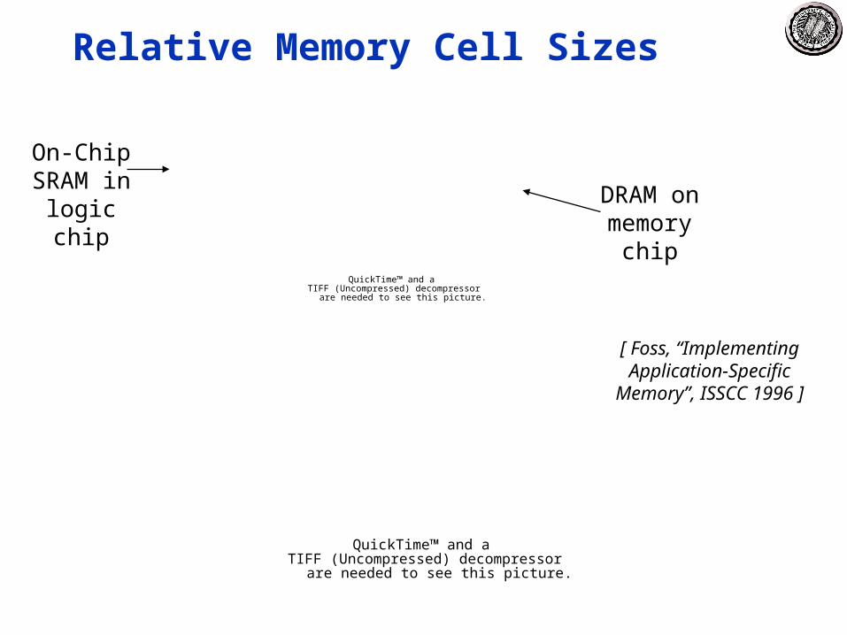
Relative Memory Cell Sizes
QuickTime™ and aTIFF (Uncompressed) decompressor
are needed to see this picture.
[ Foss, “Implementing Application-Specific
Memory”, ISSCC 1996 ]
QuickTime™ and aTIFF (Uncompressed) decompressor
are needed to see this picture.
DRAM on memory
chip
On-Chip SRAM in logic chip

2/14/2008 CS152-Spring’08 4
Placement Policy
0 1 2 3 4 5 6 7
0 1 2 3
Set Number
Cache
Fully (2-way) Set DirectAssociative Associative Mappedanywhere anywhere in only into
set 0 block 4 (12 mod 4) (12 mod 8)
0 1 2 3 4 5 6 7 8 9
1 1 1 1 1 1 1 1 1 1 0 1 2 3 4 5 6 7 8 9
2 2 2 2 2 2 2 2 2 2 0 1 2 3 4 5
6 7 8 9
3 30 1
Memory
Block Number
block 12 can be placed

2/14/2008 CS152-Spring’08
Direct-Mapped Cache
Tag Data Block V
=
BlockOffset
Tag Index
t k b
t
HIT Data Word or Byte
2k
lines

2/14/2008 CS152-Spring’08
2-Way Set-Associative Cache
Tag Data Block V
=
BlockOffset
Tag Index
t k
b
HIT
Tag Data Block V
DataWordor Byte
=
t

2/14/2008 CS152-Spring’08
Fully Associative Cache
Tag Data Block V
=
Block
Offset
Tag
t
b
HIT
DataWordor Byte
=
=
t

2/14/2008 CS152-Spring’08 8
Replacement Policy
In an associative cache, which block from a set should be evicted when the set becomes full?
• Random
• Least Recently Used (LRU)• LRU cache state must be updated on every access• true implementation only feasible for small sets (2-way)• pseudo-LRU binary tree often used for 4-8 way
• First In, First Out (FIFO) a.k.a. Round-Robin• used in highly associative caches
• Not Least Recently Used (NLRU)• FIFO with exception for most recently used block or blocks
This is a second-order effect. Why?
Replacement only happens on misses

2/14/2008 CS152-Spring’08 9
Word3Word0 Word1 Word2
Block Size and Spatial Locality
Larger block size has distinct hardware advantages• less tag overhead• exploit fast burst transfers from DRAM• exploit fast burst transfers over wide busses
What are the disadvantages of increasing block size?
block address offsetb
2b = block size a.k.a line size (in bytes)
Split CPU address
b bits32-b bits
Tag
Block is unit of transfer between the cache and memory
4 word block, b=2
2/14/2008 CS152-Spring’08 10
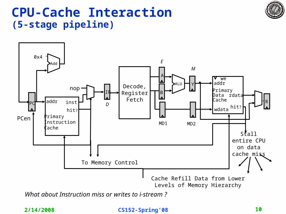
CPU-Cache Interaction(5-stage pipeline)
PC addr inst
PrimaryInstructionCache
0x4Add
IR
D
nop
hit?
PCen
Decode,RegisterFetch
wdata
R
addr
wdata
rdataPrimaryData Cache
weA
B
YYALU
MD1 MD2
Cache Refill Data from Lower Levels of Memory Hierarchy
hit?
Stall entire CPU on data
cache miss
To Memory Control
M
E
What about Instruction miss or writes to i-stream ?

2/14/2008 CS152-Spring’08 11
Improving Cache Performance
Average memory access time =Hit time + Miss rate x Miss
penalty
To improve performance:• reduce the hit time• reduce the miss rate• reduce the miss penalty
What is the simplest design strategy?

2/14/2008 CS152-Spring’08 12
Causes for Cache Misses
• Compulsory: first-reference to a block a.k.a. cold start misses
- misses that would occur even with infinite cache
• Capacity: cache is too small to hold all data needed by the program
- misses that would occur even under perfect replacement policy
• Conflict: misses that occur because of collisions due to block-placement strategy
- misses that would not occur with full associativity
2/14/2008 CS152-Spring’08 13
Effect of Cache Parameters on Performance
• Larger cache size
• Higher associativity
• Larger block size
2/14/2008 CS152-Spring’08 14
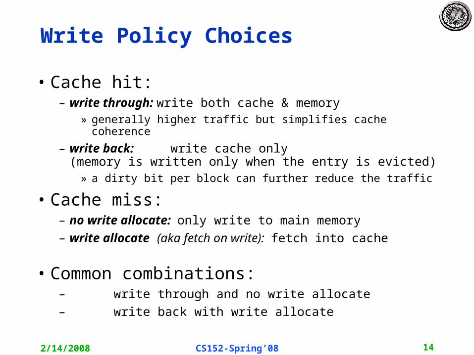
Write Policy Choices
• Cache hit:– write through: write both cache & memory
» generally higher traffic but simplifies cache coherence
– write back: write cache only (memory is written only when the entry is evicted)
» a dirty bit per block can further reduce the traffic
• Cache miss:– no write allocate: only write to main memory
– write allocate (aka fetch on write): fetch into cache
• Common combinations:– write through and no write allocate
– write back with write allocate

2/14/2008 CS152-Spring’08 15
Write Performance
Tag Data V
=
BlockOffset
Tag Index
t k
b
t
HIT Data Word or Byte
2k
lines
WE

2/14/2008 CS152-Spring’08 16
Reducing Write Hit Time
Problem: Writes take two cycles in memory stage, one cycle for tag check plus one cycle for data write if hit
Solutions:• Design data RAM that can perform read and write in one cycle,
restore old value after tag miss
• Fully-associative (CAM Tag) caches: Word line only enabled if hit
• Pipelined writes: Hold write data for store in single buffer ahead of cache, write cache data during next store’s tag check

2/14/2008 CS152-Spring’08 17
Pipelining Cache Writes
Tags Data
Tag Index Store Data
Address and Store Data From CPU
Delayed Write DataDelayed Write Addr.
=?
=?
Load Data to CPU
Load/Store
L
S
1 0
Hit?
Data from a store hit written into data portion of cache during tag access of subsequent store

2/14/2008 CS152-Spring’08 18
CS152 Administrivia
• Krste, no office hours, Monday 2/18 (President’s Day Holiday)
– email for alternate time
• Henry office hours, 511 Soda– None on Monday due to holiday
– 2:00-3:00PM Fridays
• In-class quiz dates– Q1: Tuesday February 19 (ISAs, microcode, simple pipelining)
» Material covered, Lectures 1-5, PS1, Lab 1
• We’re stuck in this room for semester (nothing else open)
2/14/2008 CS152-Spring’08 19
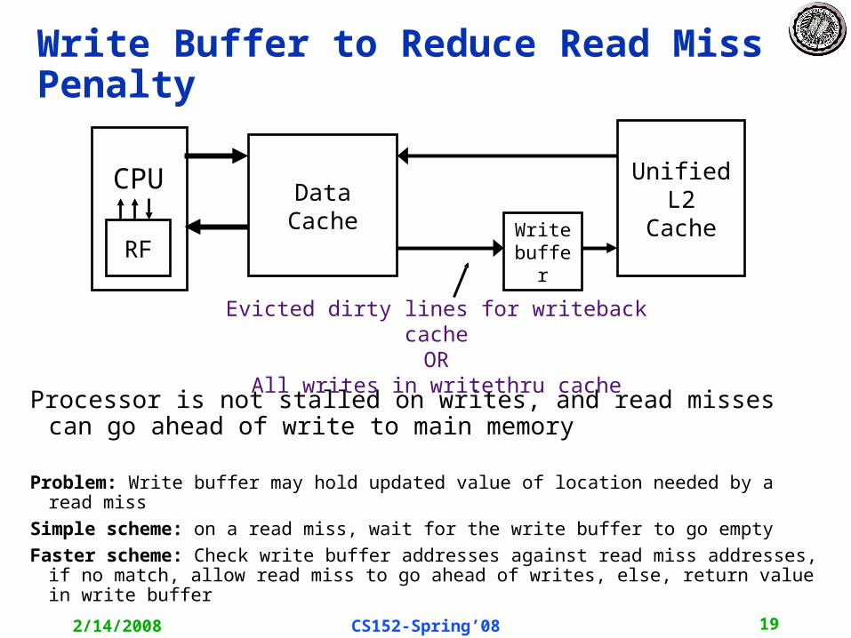
Write Buffer to Reduce Read Miss Penalty
Processor is not stalled on writes, and read misses can go ahead of write to main memory
Problem: Write buffer may hold updated value of location needed by a read miss
Simple scheme: on a read miss, wait for the write buffer to go empty
Faster scheme: Check write buffer addresses against read miss addresses, if no match, allow read miss to go ahead of writes, else, return value in write buffer
Data Cache
Unified L2
CacheRF
CPU
Writebuffer
Evicted dirty lines for writeback cacheOR
All writes in writethru cache

2/14/2008 CS152-Spring’08
Serial-versus-Parallel Cache and Memory access
is HIT RATIO: Fraction of references in cache
1 - is MISS RATIO: Remaining references
CACHEProcessor MainMemory
Addr Addr
DataDataAverage access time for serial search: tcache + (1
- ) tmem
CACHEProcessor MainMemory
Addr
DataData
Average access time for parallel search: tcache + (1 - ) tmem
• Savings are usually small, tmem >> tcache, hit ratio
high• High bandwidth required for memory path • Complexity of handling parallel paths can slow tcache

2/14/2008 CS152-Spring’08 21
Block-level Optimizations
• Tags are too large, i.e., too much overhead– Simple solution: Larger blocks, but miss penalty could be large.
• Sub-block placement (aka sector cache)– A valid bit added to units smaller than full block, called sub-blocks
– Only read a sub-block on a miss
– If a tag matches, is the word in the cache?
100
300
204
1 1 1 1
1 1 0 0
0 1 0 1
2/14/2008 CS152-Spring’08 22
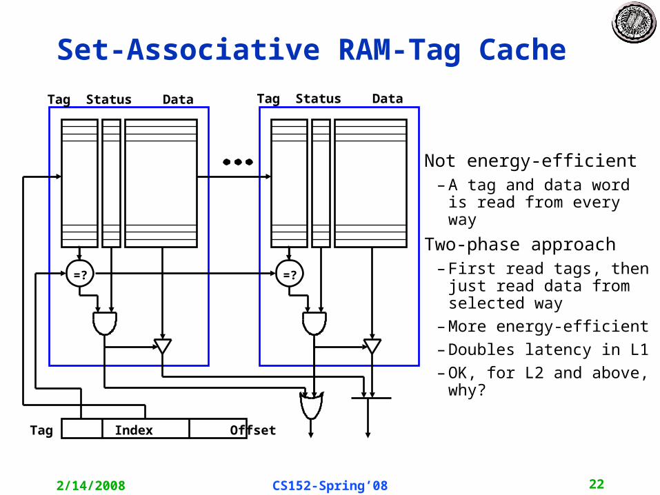
Set-Associative RAM-Tag Cache
Not energy-efficient– A tag and data word is read
from every way
Two-phase approach– First read tags, then just
read data from selected way
– More energy-efficient
– Doubles latency in L1
– OK, for L2 and above, why?
=? =?
Tag Status Data Tag Status Data
Tag Index Offset

2/14/2008 CS152-Spring’08 23
Highly-Associative CAM-Tag Caches• For high associativity (e.g., 32-way), use content-addressable memory (CAM) for
tags (ARM, Intel XScale)• Overhead: Tag+comparator bit 2-4x area of plain RAM-tag bit
Only one set enabledOnly hit data accessed – saves energy
tag set index offset
Tag =? Data BlockTag =? Data Block
Tag =? Data Block
Tag =? Data BlockTag =? Data Block
Tag =? Data Block
Tag =? Data BlockTag =? Data Block
Tag =? Data Block
Set 0Set 1Set i
Hit? Data

2/14/2008 CS152-Spring’08 24
Victim Caches (HP 7200)
L1 Data Cache
Unified L2 Cache
RF
CPU
VictimFA Cache4 blocks
Evicted datafrom L1
Evicted dataFrom VC
where ?Hit data from VC (miss in
L1)Victim cache is a small associative back up cache, added to a direct mapped cache, which holds recently evicted lines• First look up in direct mapped cache• If miss, look in victim cache• If hit in victim cache, swap hit line with line now evicted from L1• If miss in victim cache, L1 victim -> VC, VC victim->?Fast hit time of direct mapped but with reduced conflict misses

2/14/2008 CS152-Spring’08 25
Way Predicting Caches(MIPS R10000 L2 cache)
• Use processor address to index into way prediction table
• Look in predicted way at given index, then:
HIT MISS
Return copyof data fromcache
Look in other way
Read block of data from next level of cache
MISSSLOW HIT(change entry in prediction table)

2/14/2008 CS152-Spring’08 26
Multilevel Caches
• A memory cannot be large and fast• Increasing sizes of cache at each level
CPU L1 L2 DRAM
Local miss rate = misses in cache / accesses to cache
Global miss rate = misses in cache / CPU memory accesses
Misses per instruction = misses in cache / number of instructions
2/14/2008 CS152-Spring’08 27
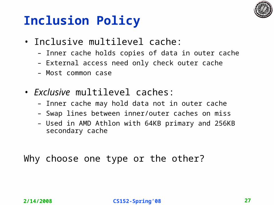
Inclusion Policy
• Inclusive multilevel cache: – Inner cache holds copies of data in outer cache
– External access need only check outer cache
– Most common case
• Exclusive multilevel caches:– Inner cache may hold data not in outer cache
– Swap lines between inner/outer caches on miss
– Used in AMD Athlon with 64KB primary and 256KB secondary cache
Why choose one type or the other?

2/14/2008 CS152-Spring’08 28
A Typical Memory Hierarchy c.2008
L1 Data Cache
L1 Instruction Cache
Unified L2 Cache
RF Memory
Memory
Memory
Memory
Multiported register
file (part of CPU)
Split instruction & data primary caches (on-chip SRAM)
Multiple interleaved memory banks
(off-chip DRAM)
Large unified secondary cache (on-chip SRAM)
CPU

2/14/2008 CS152-Spring’08 29
Itanium-2 On-Chip Caches(Intel/HP, 2002)
Level 1, 16KB, 4-way s.a., 64B line, quad-port (2 load+2 store), single cycle latency
Level 2, 256KB, 4-way s.a, 128B line, quad-port (4 load or 4 store), five cycle latency
Level 3, 3MB, 12-way s.a., 128B line, single 32B port, twelve cycle latency
2/14/2008 CS152-Spring’08 30
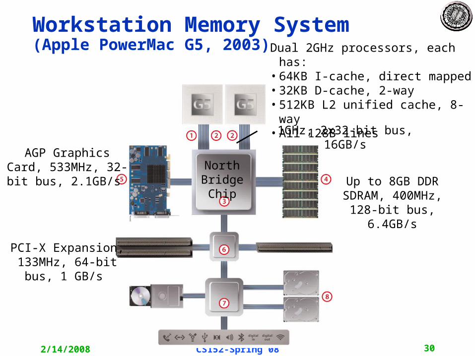
Workstation Memory System(Apple PowerMac G5, 2003) Dual 2GHz processors, each
has:•64KB I-cache, direct mapped•32KB D-cache, 2-way•512KB L2 unified cache, 8-way
•All 128B lines
Up to 8GB DDR SDRAM, 400MHz, 128-bit bus,
6.4GB/s
1GHz, 2x32-bit bus, 16GB/s
North Bridge Chip
AGP Graphics Card, 533MHz, 32-bit bus, 2.1GB/s
PCI-X Expansion, 133MHz, 64-bit bus, 1 GB/s

2/14/2008 CS152-Spring’08 31
Acknowledgements
• These slides contain material developed and copyright by:
– Arvind (MIT)
– Krste Asanovic (MIT/UCB)
– Joel Emer (Intel/MIT)
– James Hoe (CMU)
– John Kubiatowicz (UCB)
– David Patterson (UCB)
• MIT material derived from course 6.823
• UCB material derived from course CS252