cs 152 / fall 02 lec 19.1 cs 152: computer architecture and engineering lecture 19 locality and...
TRANSCRIPT
CS 152 / Fall 02 Lec 19.1
CS 152: Computer Architecture
and Engineering
Lecture 19
Locality and Memory Technologies
Randy H. Katz, InstructorSatrajit Chatterjee, Teaching Assistant
George Porter, Teaching Assistant

CS 152 / Fall 02 Lec 19.2
The Five Classic Components of a Computer
Today’s Topics: • Recap last lecture
• Locality and Memory Hierarchy
• Administrivia
• SRAM Memory Technology
• DRAM Memory Technology
• Memory Organization
The Big Picture: Where are We Now?
Control
Datapath
Memory
Processor
Input
Output

CS 152 / Fall 02 Lec 19.3
Technology Trends (From 1st Lecture)
DRAM
Year Size Cycle Time
1980 64 Kb 250 ns
1983 256 Kb 220 ns
1986 1 Mb 190 ns
1989 4 Mb 165 ns
1992 16 Mb 145 ns
1995 64 Mb 120 ns
Capacity Speed (latency)
Logic: 2x in 3 years 2x in 3 years
DRAM: 4x in 3 years 2x in 10 years
Disk: 4x in 3 years 2x in 10 years
1000:1! 2:1!
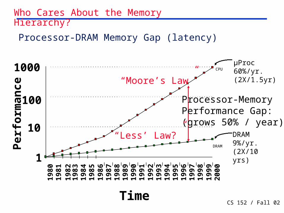
CS 152 / Fall 02 Lec 19.4
µProc60%/yr.(2X/1.5yr)
DRAM9%/yr.(2X/10 yrs)
1
10
100
1000
198
0198
1 198
3198
4198
5 198
6198
7198
8198
9199
0199
1 199
2199
3199
4199
5199
6199
7199
8 199
9200
0
DRAM
CPU198
2
Processor-MemoryPerformance Gap:(grows 50% / year)
Per
form
ance
Time
“Moore’s Law”
Processor-DRAM Memory Gap (latency)
Who Cares About the Memory Hierarchy?
“Less’ Law?”
CS 152 / Fall 02 Lec 19.5
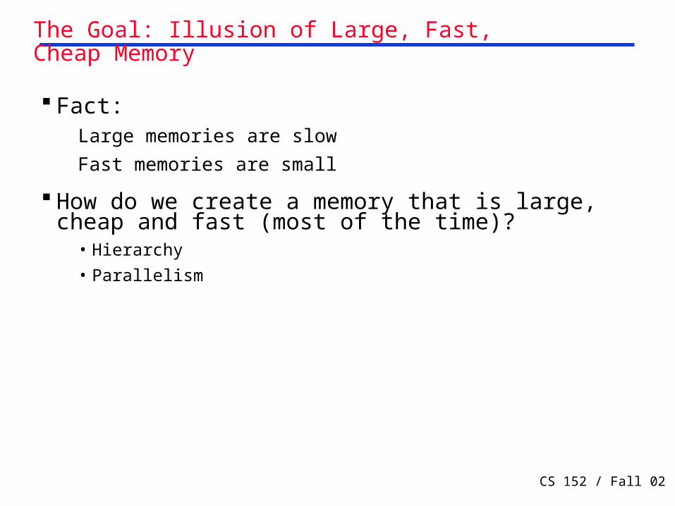
The Goal: Illusion of Large, Fast, Cheap Memory
Fact: Large memories are slow
Fast memories are small
How do we create a memory that is large, cheap and fast (most of the time)?
• Hierarchy
• Parallelism

CS 152 / Fall 02 Lec 19.6
Memory Hierarchy of a Modern Computer System By taking advantage of the principle of locality:
• Present the user with as much memory as is available in the cheapest technology.
• Provide access at the speed offered by the fastest technology.
Control
Datapath
SecondaryStorage(Disk)
Processor
Registe
rs
MainMemory(DRAM)
SecondLevelCache(SRAM)
On-C
hip
Cach
e
1s 10,000,000s
(10s ms)
Speed (ns): 10s 100s
100s GsSize (bytes): Ks Ms
TertiaryStorage(Tape)
10,000,000,000s
(10s sec)Ts

CS 152 / Fall 02 Lec 19.7
Memory Hierarchy: Why Does it Work? Locality!
Temporal Locality (Locality in Time):=> Keep most recently accessed data items closer to the
processor
Spatial Locality (Locality in Space):=> Move blocks consists of contiguous words to the upper levels
Lower LevelMemoryUpper Level
MemoryTo Processor
From ProcessorBlk X
Blk Y
Address Space0 2^n - 1
Probabilityof reference
CS 152 / Fall 02 Lec 19.8
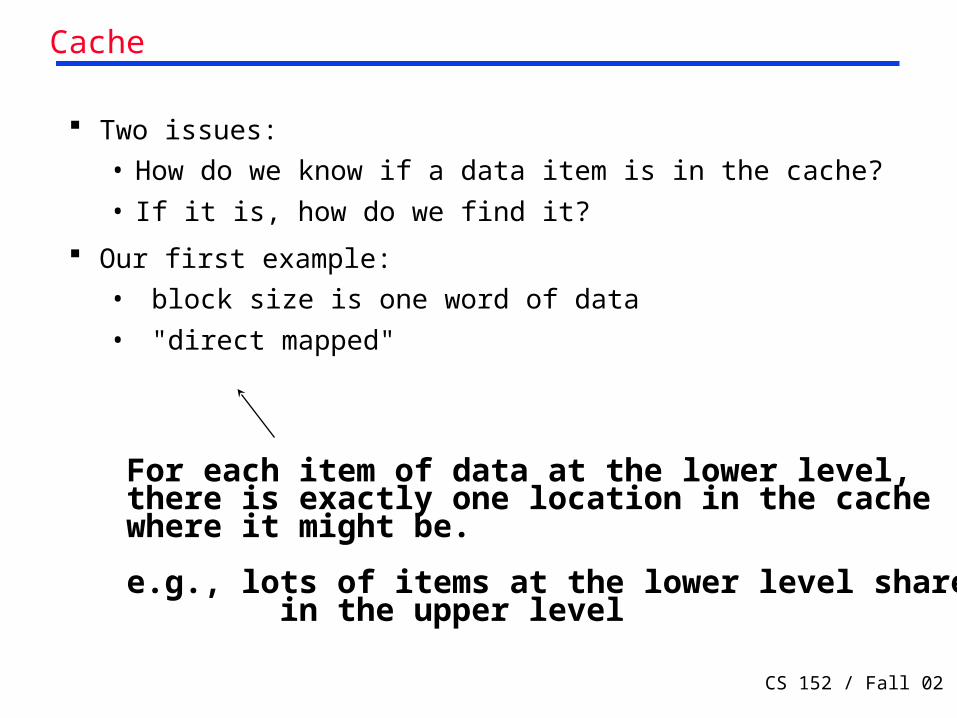
Two issues:• How do we know if a data item is in the cache?
• If it is, how do we find it?
Our first example:• block size is one word of data
• "direct mapped"
For each item of data at the lower level, there is exactly one location in the cache where it might be.
e.g., lots of items at the lower level share locations in the upper level
Cache
CS 152 / Fall 02 Lec 19.9
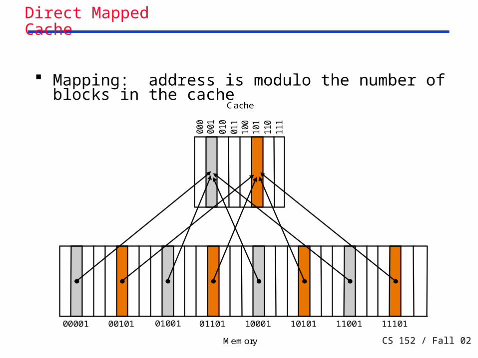
Mapping: address is modulo the number of blocks in the cache
Direct Mapped Cache
00001 00101 01001 01101 10001 10101 11001 11101
000
Cache
Memory
001
010
011
100
101
110
111

CS 152 / Fall 02 Lec 19.10
For MIPS:
What kind of locality are we taking advantage of?
Direct Mapped CacheAddress (showing bit positions)
20 10
Byteoffset
Valid Tag DataIndex
0
1
2
1021
1022
1023
Tag
Index
Hit Data
20 32
31 30 13 12 11 2 1 0

CS 152 / Fall 02 Lec 19.11
Taking advantage of spatial locality:
Direct Mapped Cache
Address (showing bit positions)
16 12 Byteoffset
V Tag Data
Hit Data
16 32
4Kentries
16 bits 128 bits
Mux
32 32 32
2
32
Block offsetIndex
Tag
31 16 15 4 32 1 0

CS 152 / Fall 02 Lec 19.12
Example: 1 KB Direct Mapped Cache with 32 B Blocks For a 2 ** N byte cache:
• The uppermost (32 - N) bits are always the Cache Tag
• The lowest M bits are the Byte Select (Block Size = 2 ** M)
Cache Index
0
1
2
3
:
Cache Data
Byte 0
0431
:
Cache Tag Example: 0x50
Ex: 0x01
0x50
Stored as partof the cache “state”
Valid Bit
:
31
Byte 1Byte 31 :
Byte 32Byte 33Byte 63 :Byte 992Byte 1023 :
Cache Tag
Byte Select
Ex: 0x00
9Block address

CS 152 / Fall 02 Lec 19.13
Read hits• this is what we want!
Read misses• stall the CPU, fetch block from memory, deliver to cache, restart
Write hits:• can replace data in cache and memory (write-through)
• write the data only into the cache (write-back the cache later)
Write misses:• read the entire block into the cache, then write the word
Hits vs. Misses

CS 152 / Fall 02 Lec 19.14
Read:
1. Send the address to the appropriate cache from PC instruction cache
from ALU data cache
2. Hit: the required word is available on the data lines
Miss: send send full address to the main memory, when the memory returns with the data, we write it into the cache
Write:
1. Index the cache using bits 15~2 of the address.
2. write both the tag portion and the data portion with word
3. also write the word to main memory using the entire address
Hits vs. Misses (Write through)

CS 152 / Fall 02 Lec 19.15
Example: Set Associative Cache N-way set associative: N entries for each Cache
Index• N direct mapped caches operates in parallel
Example: Two-way set associative cache• Cache Index selects a “set” from the cache
• The two tags in the set are compared to the input in parallel
• Data is selected based on the tag resultCache Data
Cache Block 0
Cache TagValid
:: :
Cache Data
Cache Block 0
Cache Tag Valid
: ::
Cache Index
Mux 01Sel1 Sel0
Cache Block
CompareAdr Tag
Compare
OR
Hit

CS 152 / Fall 02 Lec 19.16
Memory Hierarchy: Terminology Hit: data appears in some block in the upper level
(example: Block X) • Hit Rate: the fraction of memory access found in the upper
level
• Hit Time: Time to access the upper level which consists of
RAM access time + Time to determine hit/miss
Miss: data needs to be retrieve from a block in the lower level (Block Y)
• Miss Rate = 1 - (Hit Rate)
• Miss Penalty: Time to replace a block in the upper level +
Time to deliver the block the processor
Hit Time << Miss Penalty Lower LevelMemoryUpper Level
MemoryTo Processor
From ProcessorBlk X
Blk Y

CS 152 / Fall 02 Lec 19.17
Recap: Cache Performance
CPU time = (CPU execution clock cycles + Memory stall clock cycles) x clock cycle time
Memory stall clock cycles = (Reads x Read miss rate x Read miss penalty + Writes x Write miss rate x Write miss penalty)
Memory stall clock cycles = Memory accesses x Miss rate x Miss penalty
Different measure: AMAT
Average Memory Access time (AMAT) = Hit Time + (Miss Rate x Miss Penalty)
Note: memory hit time is included in execution cycles.

CS 152 / Fall 02 Lec 19.18
DataMiss(1.6)49%
Ideal CPI(1.1)35%
Inst Miss(0.5)16%
Recap: Impact on Performance
Suppose a processor executes at • Clock Rate = 200 MHz (5 ns per cycle)• Base CPI = 1.1 • 50% arith/logic, 30% ld/st, 20% control
Suppose that 10% of memory operations get 50 cycle miss penalty
Suppose that 1% of instructions get same miss penalty
CPI = Base CPI + average stalls per instruction 1.1(cycles/ins) +
[ 0.30 (DataMops/ins) x 0.10 (miss/DataMop) x 50
(cycle/miss)] +[ 1 (InstMop/ins)
x 0.01 (miss/InstMop) x 50 (cycle/miss)] = (1.1 + 1.5 + .5) cycle/ins = 3.1

CS 152 / Fall 02 Lec 19.19
How is the Hierarchy Managed?
Registers <-> Memory• by compiler (programmer?)
cache <-> memory• by the hardware
memory <-> disks• by the hardware and operating system (virtual memory)
• by the programmer (files)

CS 152 / Fall 02 Lec 19.20
Memory Hierarchy Technology Random Access:
• “Random” is good: access time is the same for all locations• DRAM: Dynamic Random Access Memory
- High density, low power, cheap, slow- Dynamic: need to be “refreshed” regularly
• SRAM: Static Random Access Memory- Low density, high power, expensive, fast- Static: content will last “forever”(until lose power)
“Non-so-random” Access Technology:• Access time varies from location to location and from time to time• Examples: Disk, CDROM, DRAM page-mode access
Sequential Access Technology: access time linear in location (e.g.,Tape)
Next two lectures will concentrate on random access technology• The Main Memory: DRAMs + Caches: SRAMs

CS 152 / Fall 02 Lec 19.21
Main Memory Background Performance of Main Memory:
• Latency: Cache Miss Penalty
- Access Time: time between request and word arrives
- Cycle Time: time between requests
• Bandwidth: I/O & Large Block Miss Penalty (L2)
Main Memory is DRAM : Dynamic Random Access Memory
• Dynamic since needs to be refreshed periodically (8 ms)
• Addresses divided into 2 halves (Memory as a 2D matrix):
- RAS or Row Access Strobe
- CAS or Column Access Strobe
Cache uses SRAM : Static Random Access Memory• No refresh (6 transistors/bit vs. 1 transistor)
Size: DRAM/SRAM 4-8 Cost/Cycle time: SRAM/DRAM 8-16

CS 152 / Fall 02 Lec 19.22
Random Access Memory (RAM) Technology
Why do computer designers need to know about RAM technology?
• Processor performance is usually limited by memory bandwidth
• As IC densities increase, lots of memory will fit on processor chip
- Tailor on-chip memory to specific needs
- Instruction cache
- Data cache
- Write buffer
What makes RAM different from a bunch of flip-flops?
• Density: RAM is much denser

CS 152 / Fall 02 Lec 19.23
Static RAM Cell
6-Transistor SRAM Cell
bit bit
word(row select)
bit bit
word
Write:1. Drive bit lines (bit=1, bit=0)
2.. Select row
Read:1. Precharge bit and bit to Vdd or Vdd/2 => make sure equal!
2.. Select row
3. Cell pulls one line low
4. Sense amp on column detects difference between bit and bit
replaced with pullupto save area
10
0 1

CS 152 / Fall 02 Lec 19.24
Typical SRAM Organization: 16-word x 4-bit
SRAMCell
SRAMCell
SRAMCell
SRAMCell
SRAMCell
SRAMCell
SRAMCell
SRAMCell
SRAMCell
SRAMCell
SRAMCell
SRAMCell
- +Sense Amp - +Sense Amp - +Sense Amp - +Sense Amp
: : : :
Word 0
Word 1
Word 15
Dout 0Dout 1Dout 2Dout 3
- +Wr Driver &Precharger - +
Wr Driver &Precharger - +
Wr Driver &Precharger - +
Wr Driver &Precharger
Addre
ss Deco
der
WrEnPrecharge
Din 0Din 1Din 2Din 3
A0
A1
A2
A3
Q: Which is longer:word line or
bit line?

CS 152 / Fall 02 Lec 19.25
Write Enable is usually active low (WE_L)
Din and Dout are combined to save pins:• A new control signal, output enable (OE_L) is needed
• WE_L is asserted (Low), OE_L is disasserted (High)
- D serves as the data input pin
• WE_L is disasserted (High), OE_L is asserted (Low)
- D is the data output pin
• Both WE_L and OE_L are asserted:
- Result is unknown. Don’t do that!!!
Although could change VHDL to do what desire, must do the best with what you’ve got (vs. what you need)
A
DOE_L
2Nwordsx M bitSRAM
N
M
WE_L
Logic Diagram of a Typical SRAM

CS 152 / Fall 02 Lec 19.26
Typical SRAM Timing
Write Timing:
D
Read Timing:
WE_L
A
WriteHold Time
Write Setup Time
A
DOE_L
2Nwordsx M bitSRAM
N
M
WE_L
Data In
Write Address
OE_L
High Z
Read Address
Junk
Read AccessTime
Data Out
Read AccessTime
Data Out
Read Address

CS 152 / Fall 02 Lec 19.27
Problems with SRAM
Six transistors use up a lot of area
Consider a “Zero” is stored in the cell:• Transistor N1 will try to pull “bit” to 0
• Transistor P2 will try to pull “bit bar” to 1
But bit lines are precharged to high: Are P1 and P2 necessary?
bit = 1 bit = 0
Select = 1
On Off
Off On
N1 N2
P1 P2
OnOn
CS 152 / Fall 02 Lec 19.28
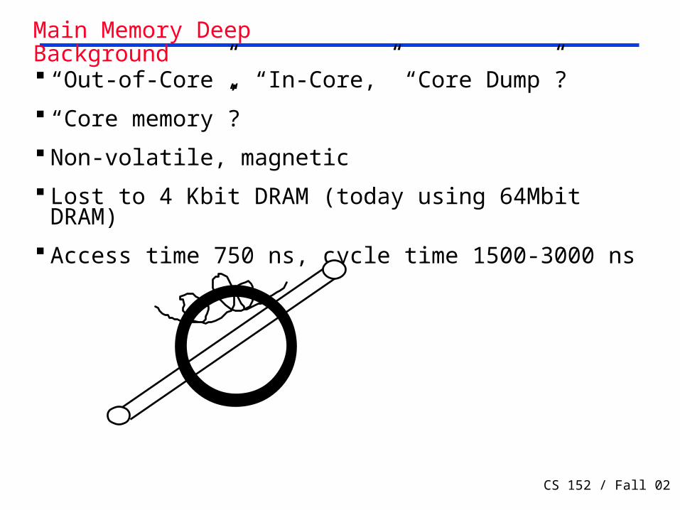
“ Out-of-Core”, “In-Core,” “Core Dump”?
“Core memory”?
Non-volatile, magnetic
Lost to 4 Kbit DRAM (today using 64Mbit DRAM)
Access time 750 ns, cycle time 1500-3000 ns
Main Memory Deep Background

CS 152 / Fall 02 Lec 19.29
1-Transistor Memory Cell (DRAM)
Write:• 1. Drive bit line
• 2.. Select row
Read:• 1. Precharge bit line to Vdd/2
• 2.. Select row
• 3. Cell and bit line share charges
- Very small voltage changes on the bit line
• 4. Sense (fancy sense amp)
- Can detect changes of ~1 million electrons
• 5. Write: restore the value
Refresh• 1. Just do a dummy read to every cell.
row select
bit
CS 152 / Fall 02 Lec 19.30
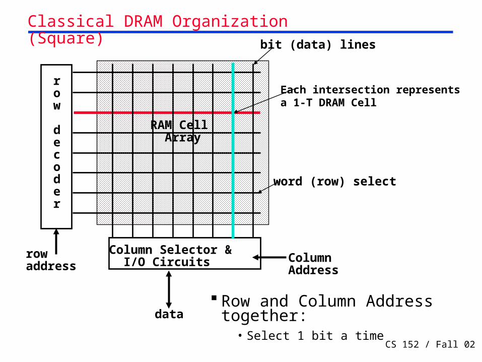
Classical DRAM Organization (Square)
row
decoder
rowaddress
Column Selector & I/O Circuits Column
Address
data
RAM Cell Array
word (row) select
bit (data) lines
Row and Column Address together:
• Select 1 bit a time
Each intersection representsa 1-T DRAM Cell
CS 152 / Fall 02 Lec 19.31
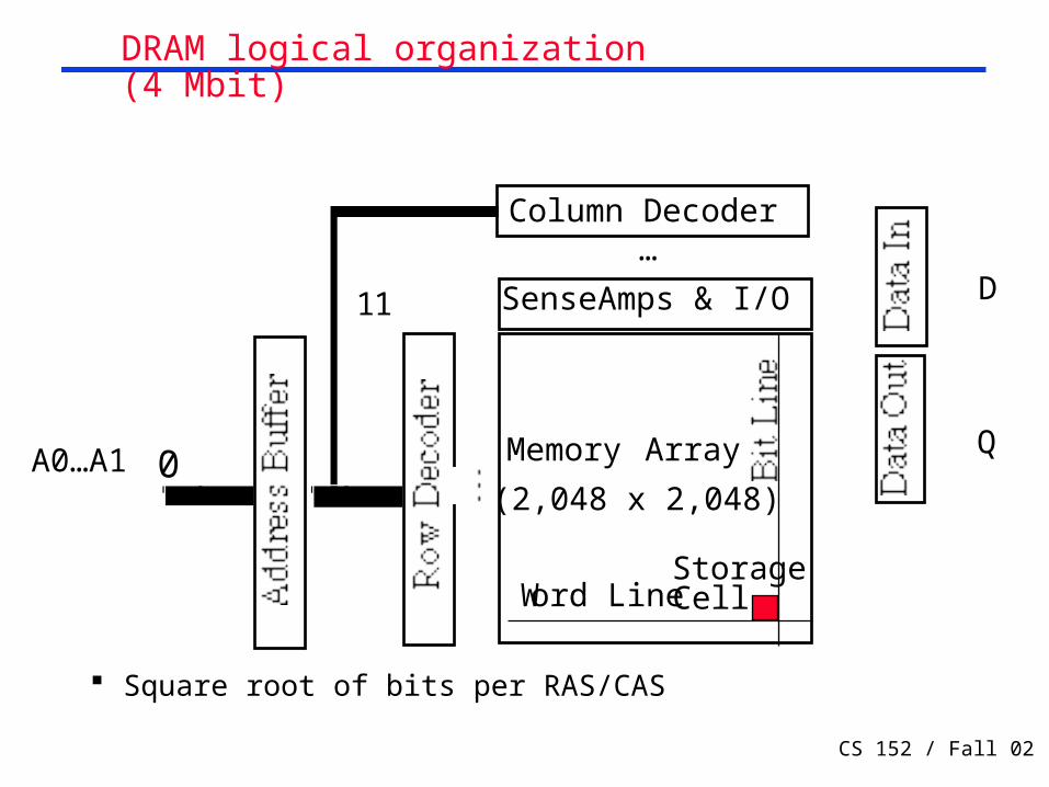
DRAM logical organization (4 Mbit)
Square root of bits per RAS/CAS
Column Decoder
Sense Amps & I/O
Memory Array
(2,048 x 2,048)A0…A1 0
…
11 D
Q
Word LineStorage Cell

CS 152 / Fall 02 Lec 19.32
Block Row Dec.9 : 512
RowBlock
Row Dec.9 : 512
Column Address
… BlockRow Dec.9 : 512
BlockRow Dec.9 : 512
…
Block 0 Block 3…
I/OI/O
I/OI/O
I/OI/O
I/OI/O
D
Q
Address
2
8 I/Os
8 I/Os
DRAM physical organization (4 Mbit)

CS 152 / Fall 02 Lec 19.33
AD
OE_L
256K x 8DRAM9 8
WE_L
Control Signals (RAS_L, CAS_L, WE_L, OE_L) are all active low
Din and Dout are combined (D):• WE_L is asserted (Low), OE_L is disasserted (High)
- D serves as the data input pin
• WE_L is disasserted (High), OE_L is asserted (Low)
- D is the data output pin
Row and column addresses share the same pins (A)
• RAS_L goes low: Pins A are latched in as row address
• CAS_L goes low: Pins A are latched in as column address
• RAS/CAS edge-sensitive
CAS_LRAS_L
Logic Diagram of a Typical DRAM
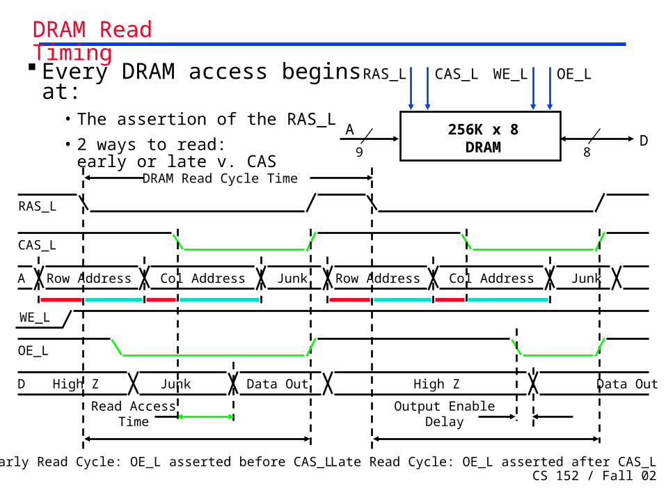
CS 152 / Fall 02 Lec 19.34
AD
OE_L
256K x 8DRAM9 8
WE_LCAS_LRAS_L
OE_L
A Row Address
WE_L
Junk
Read AccessTime
Output EnableDelay
CAS_L
RAS_L
Col Address Row Address JunkCol Address
D High Z Data Out
DRAM Read Cycle Time
Early Read Cycle: OE_L asserted before CAS_L Late Read Cycle: OE_L asserted after CAS_L
Every DRAM access begins at:
• The assertion of the RAS_L
• 2 ways to read: early or late v. CAS
Junk Data Out High Z
DRAM Read Timing

CS 152 / Fall 02 Lec 19.35
AD
OE_L
256K x 8DRAM9 8
WE_LCAS_LRAS_L
WE_L
A Row Address
OE_L
Junk
WR Access Time WR Access Time
CAS_L
RAS_L
Col Address Row Address JunkCol Address
D Junk JunkData In Data In Junk
DRAM WR Cycle Time
Early Wr Cycle: WE_L asserted before CAS_L Late Wr Cycle: WE_L asserted after CAS_L
Every DRAM access begins at:
• The assertion of the RAS_L
• 2 ways to write: early or late v. CAS
DRAM Write Timing

CS 152 / Fall 02 Lec 19.36
Key DRAM Timing Parameters tRAC: minimum time from RAS line falling to
the valid data output. • Quoted as the speed of a DRAM
• A fast 4Mb DRAM tRAC = 60 ns
tRC: minimum time from the start of one row access to the start of the next.
• tRC = 110 ns for a 4Mbit DRAM with a tRAC of 60 ns
tCAC: minimum time from CAS line falling to valid data output.
• 15 ns for a 4Mbit DRAM with a tRAC of 60 ns
tPC: minimum time from the start of one column access to the start of the next.
• 35 ns for a 4Mbit DRAM with a tRAC of 60 ns

CS 152 / Fall 02 Lec 19.37
DRAM Performance
A 60 ns (tRAC) DRAM can • perform a row access only every 110 ns (tRC)
• perform column access (tCAC) in 15 ns, but time between column accesses is at least 35 ns (tPC).
- In practice, external address delays and turning around buses make it 40 to 50 ns
These times do not include the time to drive the addresses off the microprocessor nor the memory controller overhead.
• Drive parallel DRAMs, external memory controller, bus to turn around, SIMM module, pins…
• 180 ns to 250 ns latency from processor to memory is good for a “60 ns” (tRAC) DRAM

CS 152 / Fall 02 Lec 19.38
Simple: • CPU, Cache, Bus, Memory
same width (32 bits)
Interleaved: • CPU, Cache, Bus 1 word:
Memory N Modules(4 Modules); example is word interleaved
Wide: • CPU/Mux 1 word;
Mux/Cache, Bus, Memory N words (Alpha: 64 bits & 256 bits)
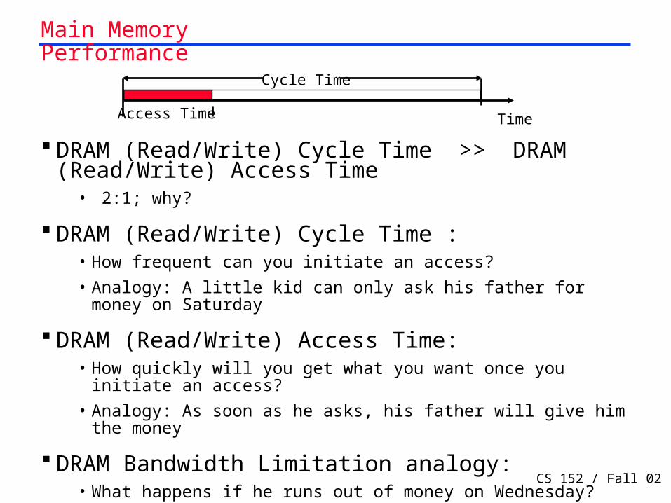
Main Memory Performance
CS 152 / Fall 02 Lec 19.39
DRAM (Read/Write) Cycle Time >> DRAM (Read/Write) Access Time
• 2:1; why?
DRAM (Read/Write) Cycle Time :• How frequent can you initiate an access?
• Analogy: A little kid can only ask his father for money on Saturday
DRAM (Read/Write) Access Time:• How quickly will you get what you want once you initiate an
access?
• Analogy: As soon as he asks, his father will give him the money
DRAM Bandwidth Limitation analogy:• What happens if he runs out of money on Wednesday?
TimeAccess Time
Cycle Time
Main Memory Performance

CS 152 / Fall 02 Lec 19.40
Access Pattern without Interleaving:
Start Access for D1
CPU Memory
Start Access for D2
D1 available
Access Pattern with 4-way Interleaving:
Acc
ess
Bank
0
Access Bank 1
Access Bank 2
Access Bank 3
We can Access Bank 0 again
CPU
MemoryBank 1
MemoryBank 0
MemoryBank 3
MemoryBank 2
Increasing Bandwidth - Interleaving
CS 152 / Fall 02 Lec 19.41
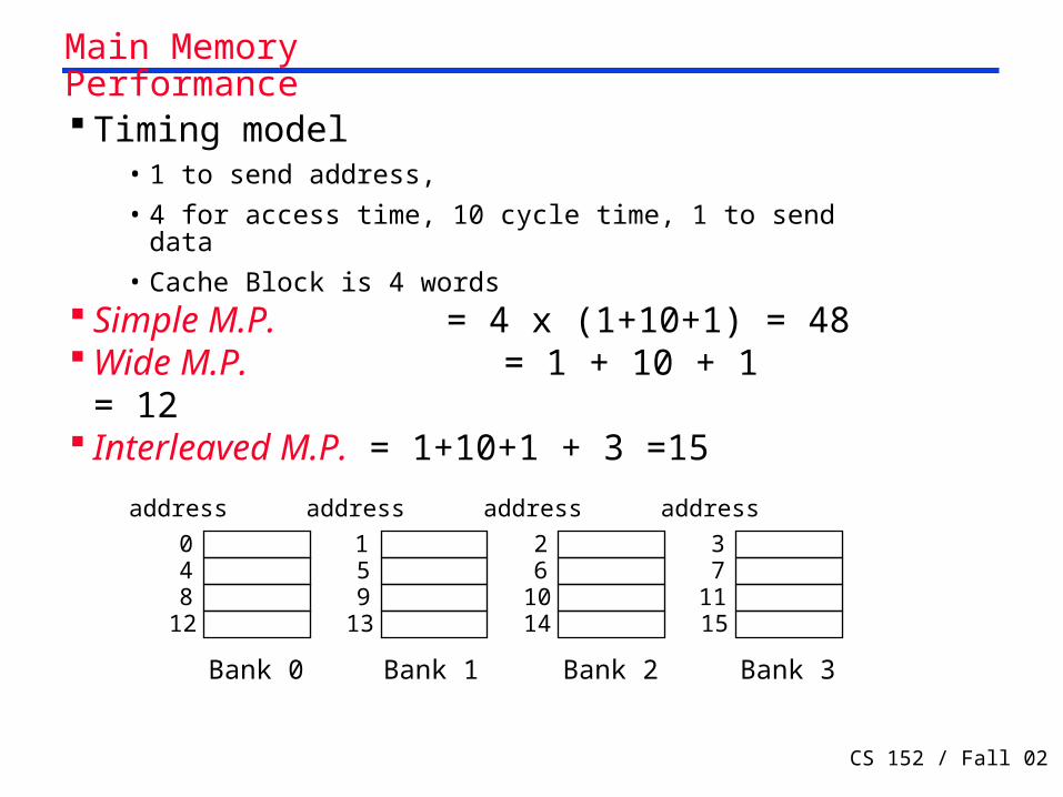
Timing model• 1 to send address,
• 4 for access time, 10 cycle time, 1 to send data
• Cache Block is 4 words Simple M.P. = 4 x (1+10+1) = 48 Wide M.P. = 1 + 10 + 1 = 12 Interleaved M.P. = 1+10+1 + 3 =15
address
Bank 0
048
12
address
Bank 1
159
13
address
Bank 2
26
1014
address
Bank 3
37
1115
Main Memory Performance
CS 152 / Fall 02 Lec 19.42
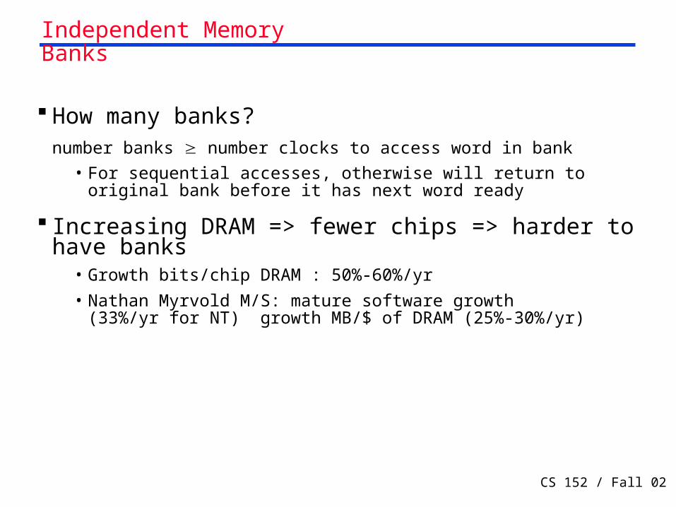
How many banks?number banks number clocks to access word in bank
• For sequential accesses, otherwise will return to original bank before it has next word ready
Increasing DRAM => fewer chips => harder to have banks
• Growth bits/chip DRAM : 50%-60%/yr
• Nathan Myrvold M/S: mature software growth (33%/yr for NT) growth MB/$ of DRAM (25%-30%/yr)
Independent Memory Banks

CS 152 / Fall 02 Lec 19.43
Two Different Types of Locality:• Temporal Locality (Locality in Time): If an item is referenced, it
will tend to be referenced again soon.
• Spatial Locality (Locality in Space): If an item is referenced, items whose addresses are close by tend to be referenced soon.
By taking advantage of the principle of locality:• Present the user with as much memory as is available in the
cheapest technology.
• Provide access at the speed offered by the fastest technology.
DRAM is slow but cheap and dense:• Good choice for presenting the user with a BIG memory system
SRAM is fast but expensive and not very dense:• Good choice for providing the user FAST access time.
Summary:

CS 152 / Fall 02 Lec 19.44
Processor % Area %Transistors
( cost) ( power)
Alpha 21164 37% 77%
StrongArm SA110 61% 94%
Pentium Pro 64% 88%• 2 dies per package: Proc/I$/D$ + L2$
Caches have no inherent value, only try to close performance gap
Summary: Processor-Memory Performance Gap “Tax”