cs 194-6 digital systems project laboratory lecture 9 ...cs194-6/fa08/lecnotes/...cs 194-6 l9:...
TRANSCRIPT

UC Regents Fall 2008 © UCBCS 194-6 L9: Advanced Processors I
2008-11-17John Lazzaro
(www.cs.berkeley.edu/~lazzaro)
CS 194-6 Digital Systems Project Laboratory
Lecture 9: Advanced Processors I
www-inst.eecs.berkeley.edu/~cs194-6/
TA: Greg Gibeling
1

UC Regents Fall 2008 © UCBCS 194-6 L9: Advanced Processors I
Today: Beyond the 5-stage pipeline
Taxonomy of advanced processing.
Superpipelining: Increasing the number of pipeline stages.
Superscalar: Issuing several instructions in a single cycle.
Amdahl’s Law
Hardware support for Virtual Memory and Virtual Machines.
2

UC Regents Fall 2008 © UCBCS 194-6 L9: Advanced Processors I
Invented the “one ISA, many implementations” business model.
3

UC Regents Fall 2008 © UCBCS 194-6 L9: Advanced Processors I
Amdahl’s Law (of Diminishing Returns)
If enhancement “E” makes multiply infinitely fast, but other
instructions are unchanged, what is the maximum speedup “S”?
Branch16%
8%
Load16%
8%
Multiply52%
Where programspends its time
S =1
(post-enhancement %) / 100%= 2.08
1
48%/100%=
Attributed to Gene Amdahl -- “Amdahl’s Law”
What is the lesson of Amdahl’s Law?
Must enhance computers in a balanced way!
4

UC Regents Fall 2008 © UCBCS 194-6 L9: Advanced Processors I
ProgramWeWishTo RunOn N CPUs
Serial30%
Parallel70%
The program spends 30%of its time running code that can not be recoded to run in parallel.
S =1
(30 % + (70% / N) ) / 100 %
CPUs 2 3 4 5 ∞
Speedup 1.54 1.85 2.1 2.3 3.3
Amdahl’s Law in Action
S(∞)
2 3 # CPUs
5
UC Regents Fall 2008 © UCBCS 194-6 L9: Advanced Processors I
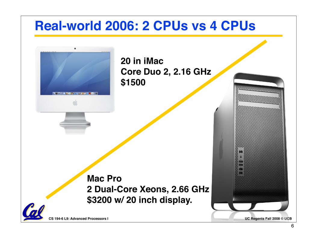
Real-world 2006: 2 CPUs vs 4 CPUs
20 in iMacCore Duo 2, 2.16 GHz$1500
Mac Pro2 Dual-Core Xeons, 2.66 GHz$3200 w/ 20 inch display.
6

UC Regents Fall 2008 © UCBCS 194-6 L9: Advanced Processors I
Real-world 2006: 2 CPUs vs 4 CPUs 2 cores on one die.
4 cores on two dies.
Caveat: Mac Pro CPUs are server-class and have architectural advantages (better I/O, ECC DRAM, ETC)
ZIPing a file: very difficult to parallelize.
Source: MACWORLD
Simple video task: easier to parallelize.
7

UC Regents Fall 2008 © UCBCS 194-6 L9: Advanced Processors I
Taxonomy
8

UC Regents Fall 2008 © UCBCS 194-6 L9: Advanced Processors I
5 Stage Pipeline: A point of departure
CS 152 L10 Pipeline Intro (9) Fall 2004 © UC Regents
Graphically Representing MIPS Pipeline
Can help with answering questions like:how many cycles does it take to execute this code?what is the ALU doing during cycle 4?is there a hazard, why does it occur, and how can it be fixed?
ALUIM Reg DM Reg
SecondsProgram
InstructionsProgram
= SecondsCycle Instruction
Cycles
At best, the 5-stage pipeline executes one instruction per
clock, with a clock period determined by the slowest stage
Filling all delay slots(branch,load)
Perfect
caching
Processor has no “multi-cycle” instructions (ex: multiply with an accumulate register)
9

UC Regents Fall 2008 © UCBCS 194-6 L9: Advanced Processors I
Superpipelining: Add more stages Today!
Seconds
Program
Instructions
Program= Seconds
Cycle Instruction
Cycles
Goal: Reduce critical path byadding more pipeline stages.
Difficulties: Added penalties for load delays and branch misses.
Ultimate Limiter: As logic delay goes to 0, FF clk-to-Q and setup.
1600 IEEE JOURNAL OF SOLID-STATE CIRCUITS, VOL. 36, NO. 11, NOVEMBER 2001
Fig. 1. Process SEM cross section.
The process was raised from [1] to limit standby power.
Circuit design and architectural pipelining ensure low voltage
performance and functionality. To further limit standby current
in handheld ASSPs, a longer poly target takes advantage of the
versus dependence and source-to-body bias is used
to electrically limit transistor in standby mode. All core
nMOS and pMOS transistors utilize separate source and bulk
connections to support this. The process includes cobalt disili-
cide gates and diffusions. Low source and drain capacitance, as
well as 3-nm gate-oxide thickness, allow high performance and
low-voltage operation.
III. ARCHITECTURE
The microprocessor contains 32-kB instruction and data
caches as well as an eight-entry coalescing writeback buffer.
The instruction and data cache fill buffers have two and four
entries, respectively. The data cache supports hit-under-miss
operation and lines may be locked to allow SRAM-like oper-
ation. Thirty-two-entry fully associative translation lookaside
buffers (TLBs) that support multiple page sizes are provided
for both caches. TLB entries may also be locked. A 128-entry
branch target buffer improves branch performance a pipeline
deeper than earlier high-performance ARM designs [2], [3].
A. Pipeline Organization
To obtain high performance, the microprocessor core utilizes
a simple scalar pipeline and a high-frequency clock. In addition
to avoiding the potential power waste of a superscalar approach,
functional design and validation complexity is decreased at the
expense of circuit design effort. To avoid circuit design issues,
the pipeline partitioning balances the workload and ensures that
no one pipeline stage is tight. The main integer pipeline is seven
stages, memory operations follow an eight-stage pipeline, and
when operating in thumb mode an extra pipe stage is inserted
after the last fetch stage to convert thumb instructions into ARM
instructions. Since thumb mode instructions [11] are 16 b, two
instructions are fetched in parallel while executing thumb in-
structions. A simplified diagram of the processor pipeline is
Fig. 2. Microprocessor pipeline organization.
shown in Fig. 2, where the state boundaries are indicated by
gray. Features that allow the microarchitecture to achieve high
speed are as follows.
The shifter and ALU reside in separate stages. The ARM in-
struction set allows a shift followed by an ALU operation in a
single instruction. Previous implementations limited frequency
by having the shift and ALU in a single stage. Splitting this op-
eration reduces the critical ALU bypass path by approximately
1/3. The extra pipeline hazard introduced when an instruction is
immediately followed by one requiring that the result be shifted
is infrequent.
Decoupled Instruction Fetch.A two-instruction deep queue is
implemented between the second fetch and instruction decode
pipe stages. This allows stalls generated later in the pipe to be
deferred by one or more cycles in the earlier pipe stages, thereby
allowing instruction fetches to proceed when the pipe is stalled,
and also relieves stall speed paths in the instruction fetch and
branch prediction units.
Deferred register dependency stalls. While register depen-
dencies are checked in the RF stage, stalls due to these hazards
are deferred until the X1 stage. All the necessary operands are
then captured from result-forwarding busses as the results are
returned to the register file.
One of the major goals of the design was to minimize the en-
ergy consumed to complete a given task. Conventional wisdom
has been that shorter pipelines are more efficient due to re-
Example: 8-stage ARM XScale:extra IF, ID, data cache stages.
Also, power!
10

UC Regents Fall 2008 © UCBCS 194-6 L9: Advanced Processors I
Seconds
Program
Instructions
Program= Seconds
Cycle Instruction
Cycles
Goal: Improve CPI by issuing several instructions per cycle.
Difficulties: Load and branchdelays affect more instructions.Ultimate Limiter: Programs maybe a poor match to issue rules.
!"#$%&
!"#$%
&'"()*+,-*.,,/
012.3-*4++556
789($:;9*<9:$*=
)'"'($%":#$:(#
>8#?
>8#?
.*(?(
.*(?(
+(?(+(?(+(?(
!"##$
%&%'#&(')
%*+,&*##$
%&%'#&(')
789($:;9*89:$#*)'@%*:9$%"9'A*B:B%A:9%*"%C:#$%"#
!"";B%"'9D#*'"%*A'$()%D*E)%9*'9*:9#$"8($:;9*
%9$%"#*'*F89($:;9*89:$*
!"":9B8$#*$;*'*F89($:;9*89:$*G%
1C1-*"%C:#$%"*F:A%
H
('9*()'9C%*D8":9C*'*A;9C*A'$%9(?*;B%"'$:;9
'((%B$
'((%B$
!"#$%
&'"()*+,-*.,,/
012.3-*4++550
&8A$:BA%*789($:;9*<9:$#
I7IJ
KL
M4<
&%N
7'DD
7N8A
7D:@
I##8%
OPQR#
7PQR#
Example: CPU with floating point ALUs: Issue 1 FP + 1 Integer instruction per cycle.
Superscalar: Multiple issues per cycle Today!
11
UC Regents Fall 2008 © UCBCS 194-6 L9: Advanced Processors I
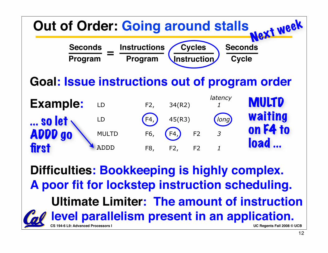
Out of Order: Going around stallsNext week
Goal: Issue instructions out of program order
Seconds
Program
Instructions
Program= Seconds
Cycle Instruction
Cycles
!"#$%&
!"#$%
&'"()*+,-*.//0
123.4-*5+.664
7869":%"*7##;%*5<=<$'$<>8#? !"#$%!&'($
!"#$%&'( !" #$%& '()*$+ (
) !" #(% (,)*'+ !*%+
, -.!/" #0% #(% #$ ,
- 1.2" #3% #$% #$ (
. "45" #(% #$% #3 -
/ 6""" #78% #0% #( (
786>":%"? +*@.-+A*2**2**2**2**2**2**. 4*0*0 4 ,*2**2**2*, 1*1
( )
,-
.
/
49:;<=><&<>?@<AB@A;9&C<>D>9@?&A9?@<EB@A;9&(&F<;G&H>A9I&=A?CJ@BK>=
!"#$%
&'"()*+,-*.//0
123.4-*5+.660
9;$6>B69":%"*C<#D'$()
7E 7C FG
H5I &%=
E'::
E=;J
7##;%
' 7##;%*#$'K%*L;BB%"*)>J:#*=;J$<DJ%*<8#$";($<>8#*M'<$<8K*
$>*<##;%2
' C%(>:%*'::#*8%N$*<8#$";($<>8*$>*L;BB%"*<B*$)%"%*<#
#D'(%*'8:*$)%*<8#$";($<>8*:>%#*8>$*(';#%*'*FHO*
>"*FHF*)'P'":2
' H8Q*<8#$";($<>8*<8*L;BB%"*M)>#%*OHF*)'P'":#*'"%
#'$<#B<%:*('8*L%*:<#D'$()%:*)*+,#"+-.#!/#&+0/#+"$
120'!/34#'$,#353($62*98*'*M"<$%*L'(R*@FGA-*8%M
<8#$";($<>8#*='Q*K%$*%8'LJ%:2
ADDD
Example: MULTDwaiting on F4 to load ...
... so let ADDD gofirst
Difficulties: Bookkeeping is highly complex.A poor fit for lockstep instruction scheduling.
Ultimate Limiter: The amount of instruction level parallelism present in an application.
12

UC Regents Fall 2008 © UCBCS 194-6 L9: Advanced Processors I
Dynamic Scheduling: End lockstepGoal: Enable out-of-order by breaking pipeline in two: Fetch and Execution.
Limiters: Design complexity, instruction level parallelism.
Example: IBM Power 5:
The Power5 scans fetched instructions forbranches (BP stage), and if it finds a branch,predicts the branch direction using threebranch history tables shared by the twothreads. Two of the BHTs use bimodal andpath-correlated branch prediction mecha-nisms to predict branch directions.6,7 Thethird BHT predicts which of these predictionmechanisms is more likely to predict the cor-
rect direction.7 If the fetched instructions con-tain multiple branches, the BP stage can pre-dict all the branches at the same time. Inaddition to predicting direction, the Power5also predicts the target of a taken branch inthe current cycle’s eight-instruction group. Inthe PowerPC architecture, the processor cancalculate the target of most branches from theinstruction’s address and offset value. For
43MARCH–APRIL 2004
MP ISS RF EA DC WB Xfer
MP ISS RF EX WB Xfer
MP ISS RF EX WB Xfer
MP ISS RF
XferF6
Group formation andinstruction decode
Instruction fetch
Branch redirects
Interrupts and flushes
WB
Fmt
D1 D2 D3 Xfer GD
BPICCP
D0
IF
Branchpipeline
Load/storepipeline
Fixed-pointpipeline
Floating-point pipeline
Out-of-order processing
Figure 3. Power5 instruction pipeline (IF = instruction fetch, IC = instruction cache, BP = branch predict, D0 = decode stage0, Xfer = transfer, GD = group dispatch, MP = mapping, ISS = instruction issue, RF = register file read, EX = execute, EA =compute address, DC = data caches, F6 = six-cycle floating-point execution pipe, Fmt = data format, WB = write back, andCP = group commit).
Shared by two threads Thread 0 resources Thread 1 resources
LSU0FXU0
LSU1
FXU1
FPU0
FPU1
BXU
CRL
Dynamicinstructionselection
Threadpriority
Group formationInstruction decode
Dispatch
Shared-register
mappers
Readshared-
register files
Sharedissue
queues
Sharedexecution
units
Alternate
Branch prediction
Instructioncache
Instructiontranslation
Programcounter
Branchhistorytables
Returnstack
Targetcache
DataCache
DataTranslation
L2cache
Datacache
Datatranslation
Instructionbuffer 0
Instructionbuffer 1
Writeshared-
register files
Groupcompletion
Storequeue
Figure 4. Power5 instruction data flow (BXU = branch execution unit and CRL = condition register logical execution unit).
Next week
13

UC Regents Fall 2008 © UCBCS 194-6 L9: Advanced Processors I
Throughput and multiple threadsGoal: Use multiple CPUs (real and virtual) to improve (1) throughput of machines that run many programs (2) execution time of multi-threaded programs.
Difficulties: Gaining full advantage requires rewriting applications, OS, libraries.
Ultimate limiter: Amdahl’s law, memory system performance.
Example: Sun Niagara (8 SPARCs on one chip).
Next week
14

UC Regents Fall 2008 © UCBCS 194-6 L9: Advanced Processors I
Superpipelining
15

UC Regents Fall 2008 © UCBCS 194-6 L9: Advanced Processors I
CS
152 L10 Pipeline Intro (9)Fall 2004 ©
UC
Regents
Graphically R
epresenting MIP
S Pipeline
Can help w
ith answering questions like:
how m
any cycles does it take to execute this code?w
hat is the ALU
doing during cycle 4?is there a hazard, w
hy does it occur, and how can it be fixed?
ALU
IMR
egD
MR
eg
IR
ID+RF
EX
MEM
WB
IR
IR
IR
IF
5 Stage1600 IEEE JOURNAL OF SOLID-STATE CIRCUITS, VOL. 36, NO. 11, NOVEMBER 2001
Fig. 1. Process SEM cross section.
The process was raised from [1] to limit standby power.
Circuit design and architectural pipelining ensure low voltage
performance and functionality. To further limit standby current
in handheld ASSPs, a longer poly target takes advantage of the
versus dependence and source-to-body bias is used
to electrically limit transistor in standby mode. All core
nMOS and pMOS transistors utilize separate source and bulk
connections to support this. The process includes cobalt disili-
cide gates and diffusions. Low source and drain capacitance, as
well as 3-nm gate-oxide thickness, allow high performance and
low-voltage operation.
III. ARCHITECTURE
The microprocessor contains 32-kB instruction and data
caches as well as an eight-entry coalescing writeback buffer.
The instruction and data cache fill buffers have two and four
entries, respectively. The data cache supports hit-under-miss
operation and lines may be locked to allow SRAM-like oper-
ation. Thirty-two-entry fully associative translation lookaside
buffers (TLBs) that support multiple page sizes are provided
for both caches. TLB entries may also be locked. A 128-entry
branch target buffer improves branch performance a pipeline
deeper than earlier high-performance ARM designs [2], [3].
A. Pipeline Organization
To obtain high performance, the microprocessor core utilizes
a simple scalar pipeline and a high-frequency clock. In addition
to avoiding the potential power waste of a superscalar approach,
functional design and validation complexity is decreased at the
expense of circuit design effort. To avoid circuit design issues,
the pipeline partitioning balances the workload and ensures that
no one pipeline stage is tight. The main integer pipeline is seven
stages, memory operations follow an eight-stage pipeline, and
when operating in thumb mode an extra pipe stage is inserted
after the last fetch stage to convert thumb instructions into ARM
instructions. Since thumb mode instructions [11] are 16 b, two
instructions are fetched in parallel while executing thumb in-
structions. A simplified diagram of the processor pipeline is
Fig. 2. Microprocessor pipeline organization.
shown in Fig. 2, where the state boundaries are indicated by
gray. Features that allow the microarchitecture to achieve high
speed are as follows.
The shifter and ALU reside in separate stages. The ARM in-
struction set allows a shift followed by an ALU operation in a
single instruction. Previous implementations limited frequency
by having the shift and ALU in a single stage. Splitting this op-
eration reduces the critical ALU bypass path by approximately
1/3. The extra pipeline hazard introduced when an instruction is
immediately followed by one requiring that the result be shifted
is infrequent.
Decoupled Instruction Fetch.A two-instruction deep queue is
implemented between the second fetch and instruction decode
pipe stages. This allows stalls generated later in the pipe to be
deferred by one or more cycles in the earlier pipe stages, thereby
allowing instruction fetches to proceed when the pipe is stalled,
and also relieves stall speed paths in the instruction fetch and
branch prediction units.
Deferred register dependency stalls. While register depen-
dencies are checked in the RF stage, stalls due to these hazards
are deferred until the X1 stage. All the necessary operands are
then captured from result-forwarding busses as the results are
returned to the register file.
One of the major goals of the design was to minimize the en-
ergy consumed to complete a given task. Conventional wisdom
has been that shorter pipelines are more efficient due to re-
8 Stage
IF now takes 2 stages (pipelined I-cache)
ID and RF each get a stage.ALU split over 3 stagesMEM takes 2 stages (pipelined D-cache)
Note: Some stages now overlap, some instructions
take extra stages.
16

UC Regents Fall 2008 © UCBCS 194-6 L9: Advanced Processors I
Superpipelining techniques ...
Split ALU and decode logic over several pipeline stages.
Pipeline memory: Use more banks of smaller arrays, add pipeline stages between decoders, muxes.
Remove “rarely-used” forwarding networks that are on critical path.
Pipeline the wires of frequently used forwarding networks.
Creates stalls, affects CPI.
Also: Clocking tricks (example: negedge register file in COD3e pipeline)
17

UC Regents Fall 2008 © UCBCS 194-6 L9: Advanced Processors I
Recall: IBM Power Timing Closure
From “The circuit and physical design of the POWER4 microprocessor”, IBM J Res and Dev, 46:1, Jan 2002, J.D. Warnock et al.
“Pipeline engineering”
happens here ...
18

UC Regents Fall 2008 © UCBCS 194-6 L9: Advanced Processors I
Recall: Pipelining SRAM memories ...4/12/04 ©UCB Spring 2004
CS152 / Kubiatowicz Lec19.13
° Why do computer designers need to know about RAM technology?
• Processor performance is usually limited by memory bandwidth
• As IC densities increase, lots of memory will fit on processor chip
- Tailor on-chip memory to specific needs
- Instruction cache
- Data cache
- Write buffer
° What makes RAM different from a bunch of flip-flops?• Density: RAM is much denser
Random Access Memory (RAM) Technology
4/12/04 ©UCB Spring 2004CS152 / Kubiatowicz
Lec19.14
Static RAM Cell
6-Transistor SRAM Cell
bit bit
word(row select)
bit bit
word
° Write:1. Drive bit lines (bit=1, bit=0)
2.. Select row
° Read:1. Precharge bit and bit to Vdd or Vdd/2 => make sure equal!
2.. Select row
3. Cell pulls one line low
4. Sense amp on column detects difference between bit and bit
replaced with pullupto save area
10
0 1
4/12/04 ©UCB Spring 2004CS152 / Kubiatowicz
Lec19.15
Typical SRAM Organization: 16-word x 4-bit
SRAM
Cell
SRAM
Cell
SRAM
Cell
SRAM
Cell
SRAM
Cell
SRAM
Cell
SRAM
Cell
SRAM
Cell
SRAM
Cell
SRAM
Cell
SRAM
Cell
SRAM
Cell
- +Sense Amp - +Sense Amp - +Sense Amp - +Sense Amp
: : : :
Word 0
Word 1
Word 15
Dout 0Dout 1Dout 2Dout 3
- +Wr Driver &
Precharger - +Wr Driver &
Precharger - +Wr Driver &
Precharger - +Wr Driver &
Precharger
Ad
dress D
eco
der
WrEn
Precharge
Din 0Din 1Din 2Din 3
A0
A1
A2
A3
Q: Which is longer:
word line or
bit line?
4/12/04 ©UCB Spring 2004CS152 / Kubiatowicz
Lec19.16
° Write Enable is usually active low (WE_L)
° Din and Dout are combined to save pins:• A new control signal, output enable (OE_L) is needed
• WE_L is asserted (Low), OE_L is disasserted (High)
- D serves as the data input pin
• WE_L is disasserted (High), OE_L is asserted (Low)
- D is the data output pin
• Both WE_L and OE_L are asserted:
- Result is unknown. Don’t do that!!!
° Although could change VHDL to do what desire, must do the best with what you’ve got (vs. what you need)
A
DOE_L
2 Nwordsx M bit
SRAM
N
M
WE_L
Logic Diagram of a Typical SRAM
WriteDriver
WriteDriver
WriteDriver
WriteDriver
Word and bit lines slow down as array grows larger! Architects specify number of rows and columns.
ParallelDataI/OLines
Add muxesto selectsubset of bits
How could we pipeline this memory?19

UC Regents Fall 2008 © UCBCS 194-6 L9: Advanced Processors I
ALU: Pipelining Unsigned Multiply
Time / Space (resource) Trade-offs
• Carry select and CLA utilize more silicon to reduce time.
• Can we use more time to reduce silicon?
• How few FAs does it take to do addition?
Bit-serial Adder
• Addition of 2 n-bit numbers:– takes n clock cycles,– uses 1 FF, 1 FA cell, plus registers– the bit streams may come from or go to other circuits, therefore
the registers may be optional.
• Requires controller– What does the FSM look like? Implemented?
• Final carry out?
• A, B, and R held in shift-registers. Shift right once per clock cycle.
• Reset is asserted by controller.
n-bit shift register
n-bit shift registers
sc
reset
R
FAFF
B
A
lsb
Announcements• Reading: 5.8• Regrades in with homework on Friday• Digital Design in the news – from UCB
– Organic e-textiles (Prof. Vivek Subramanian)
Basic concept of multiplication
!"#$%&#%'()*
!"#$%&#%+,
--.-///0-12
-.--///0--2
--.-
--.-
....
--.-
3
-...---- 0-412
5(,$%(#/&,6*"'$7
• product of 2 n-bit numbers is an 2n-bit number– sum of n n-bit partial products
• unsigned
Combinational Multiplier:accumulation of partial products
8.
9.
8./9.
8-
9-
8-/9.
8./9-
8:
9:
8:/9.
8-/9-
8./9:
81
91
8:/9.
8:/9-
8-/9:
8./91
81/9-
8:/9:
8-/91
81/9:
8:/9181/91
;< ;= ;4 ;1 ;: ;- ;.;>
Array Multiplier
b3 0 b2 0 b1 0 b0 0
P7 P6 P5 P4
a0
0
a1
0
a2
0
a3
0
P0
P1
P2
P3
FA
bj sum in
sum out
carryout
ai
carryin
Each row: n-bit adder with AND gates
What is the critical path?
Generates all n partial products simultaneously.
2/11/03 ©UCB Spring 2004CS152 / Kubiatowicz
Lec6.21
MIPS arithmetic instructions
° Instruction Example Meaning Comments
° add add $1,$2,$3 $1 = $2 + $3 3 operands; exception possible° subtract sub $1,$2,$3 $1 = $2 – $3 3 operands; exception possible° add immediate addi $1,$2,100 $1 = $2 + 100 + constant; exception possible° add unsigned addu $1,$2,$3 $1 = $2 + $3 3 operands; no exceptions° subtract unsigned subu $1,$2,$3 $1 = $2 – $3 3 operands; no exceptions° add imm. unsign. addiu $1,$2,100 $1 = $2 + 100 + constant; no exceptions° multiply mult $2,$3 Hi, Lo = $2 x $3 64-bit signed product° multiply unsigned multu$2,$3 Hi, Lo = $2 x $3 64-bit unsigned product° divide div $2,$3 Lo = $2 ÷ $3, Lo = quotient, Hi = remainder ° Hi = $2 mod $3 ° divide unsigned divu $2,$3 Lo = $2 ÷ $3, Unsigned quotient & remainder ° Hi = $2 mod $3° Move from Hi mfhi $1 $1 = Hi Used to get copy of Hi° Move from Lo mflo $1 $1 = Lo Used to get copy of Lo
2/11/03 ©UCB Spring 2004CS152 / Kubiatowicz
Lec6.22
MULTIPLY (unsigned)
° Paper and pencil example (unsigned):
Multiplicand 1000Multiplier 1001
10000000
00001000
Product 01001000
° m bits x n bits = m+n bit product
° Binary makes it easy:
•0 => place 0 ( 0 x multiplicand)
•1 => place a copy ( 1 x multiplicand)
° 4 versions of multiply hardware & algorithm:
•successive refinement
2/11/03 ©UCB Spring 2004CS152 / Kubiatowicz
Lec6.23
Unsigned Combinational Multiplier
B0
A0A1A2A3
A0A1A2A3
A0A1A2A3
A0A1A2A3
B1
B2
B3
P0P1P2P3P4P5P6P7
0 0 0 0
° Stage i accumulates A * 2 i if Bi == 1
° Q: How much hardware for 32 bit multiplier? Critical path?
2/11/03 ©UCB Spring 2004CS152 / Kubiatowicz
Lec6.24
How does it work?
A0A1A2A3
A0A1A2A3
0 0 0 00 0 0
B0
A0A1A2A3 B1
B2
A0A1A2A3 B3
P6
° At each stage shift A left ( x 2)
° Use next bit of B to determine whether to add in shifted multiplicand
° Accumulate 2n bit partial product at each stage
P0P1P2P7 P5 P4 P3
Facts to remember
1011*
20

UC Regents Fall 2008 © UCBCS 194-6 L9: Advanced Processors I
Building Block: Full-Adder Variant
CinCout
x y
z
s
1-bit signals: x, y, z, s, Cin, Cout
If z = 1, {Cout, s} <= x + y + Cin
If z = 0, {Cout, s} <= y + Cin
z: one bit of multiplierx: one bit of multiplicand
y: one bit of the “running sum”21

UC Regents Fall 2008 © UCBCS 194-6 L9: Advanced Processors I
Put it together: Array computes P = A x B
2/11/03 ©UCB Spring 2004CS152 / Kubiatowicz
Lec6.21
MIPS arithmetic instructions
° Instruction Example Meaning Comments
° add add $1,$2,$3 $1 = $2 + $3 3 operands; exception possible° subtract sub $1,$2,$3 $1 = $2 – $3 3 operands; exception possible° add immediate addi $1,$2,100 $1 = $2 + 100 + constant; exception possible° add unsigned addu $1,$2,$3 $1 = $2 + $3 3 operands; no exceptions° subtract unsigned subu $1,$2,$3 $1 = $2 – $3 3 operands; no exceptions° add imm. unsign. addiu $1,$2,100 $1 = $2 + 100 + constant; no exceptions° multiply mult $2,$3 Hi, Lo = $2 x $3 64-bit signed product° multiply unsigned multu$2,$3 Hi, Lo = $2 x $3 64-bit unsigned product° divide div $2,$3 Lo = $2 ÷ $3, Lo = quotient, Hi = remainder ° Hi = $2 mod $3 ° divide unsigned divu $2,$3 Lo = $2 ÷ $3, Unsigned quotient & remainder ° Hi = $2 mod $3° Move from Hi mfhi $1 $1 = Hi Used to get copy of Hi° Move from Lo mflo $1 $1 = Lo Used to get copy of Lo
2/11/03 ©UCB Spring 2004CS152 / Kubiatowicz
Lec6.22
MULTIPLY (unsigned)
° Paper and pencil example (unsigned):
Multiplicand 1000Multiplier 1001
10000000
00001000
Product 01001000
° m bits x n bits = m+n bit product
° Binary makes it easy:
•0 => place 0 ( 0 x multiplicand)
•1 => place a copy ( 1 x multiplicand)
° 4 versions of multiply hardware & algorithm:
•successive refinement
2/11/03 ©UCB Spring 2004CS152 / Kubiatowicz
Lec6.23
Unsigned Combinational Multiplier
B0
A0A1A2A3
A0A1A2A3
A0A1A2A3
A0A1A2A3
B1
B2
B3
P0P1P2P3P4P5P6P7
0 0 0 0
° Stage i accumulates A * 2 i if Bi == 1
° Q: How much hardware for 32 bit multiplier? Critical path?
2/11/03 ©UCB Spring 2004CS152 / Kubiatowicz
Lec6.24
How does it work?
A0A1A2A3
A0A1A2A3
0 0 0 00 0 0
B0
A0A1A2A3 B1
B2
A0A1A2A3 B3
P6
° At each stage shift A left ( x 2)
° Use next bit of B to determine whether to add in shifted multiplicand
° Accumulate 2n bit partial product at each stage
P0P1P2P7 P5 P4 P3
0 0 0 0
z
x
y
Cout
Cout
Cout
Cout
To pipeline array:
Place registers between adder stages.
Use registers to delay selectedA and B bits.
As drawn, combinational (slow!).22

UC Regents Fall 2008 © UCBCS 194-6 L9: Advanced Processors I
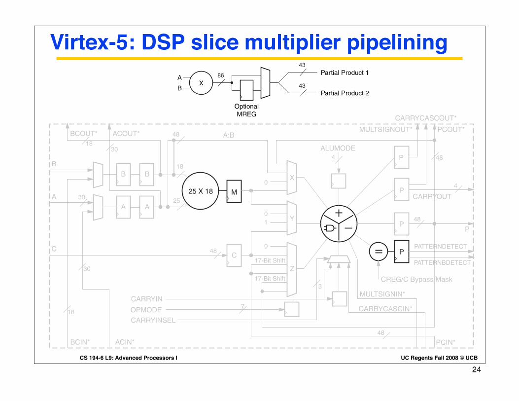
Virtex-5: DSP slice multiplier pipelining
16 www.xilinx.com Virtex-5 FPGA XtremeDSP Design ConsiderationsUG193 (v3.2) September 23, 2008
Chapter 1: DSP48E Description and SpecificsR
Architectural HighlightsThe Virtex-5 DSP48E slice includes all Virtex-4 DSP48 features plus a variety of new features. Among the new features are a wider 25 x 18 multiplier and an add/subtract function that has been extended to function as a logic unit. This logic unit can perform a host of bitwise logical operations when the multiplier is not used. The DSP48E slice includes a pattern detector and a pattern bar detector that can be used for convergent rounding, overflow/underflow detection for saturation arithmetic, and auto-resetting counters/accumulators. The Single Instruction Multiple Data (SIMD) mode of the adder/subtracter/logic unit is also new to the DSP48E slice; this mode is available when the multiplier is not used. The Virtex-5 DSP48E slice also has new cascade paths. The new features are highlighted in Figure 1-2.
Figure 1-1: Virtex-5 DSP48E Slice
X
17-Bit Shift
17-Bit Shift
0
Y
Z
10
0
48
48
184
3
48
2530
BCOUT*
BCIN* ACIN*
OPMODE
PCIN*
MULTSIGNIN*
PCOUT*
CARRYCASCOUT*
MULTSIGNOUT*
CREG/C Bypass/Mask
CARRYCASCIN*CARRYIN
CARRYINSEL
ACOUT* A:B
ALUMODE
BB
A
C
B
M
P
PP
C
25 X 18
A A
PATTERNDETECT
PATTERNBDETECT
CARRYOUT
UG193_c1_01_032806
4
7
48
4830
18
30
18
P
P
*These signals are dedicated routing paths internal to the DSP48E column. They are not accessible via fabric routing resources.
Virtex-5 FPGA XtremeDSP Design Considerations www.xilinx.com 41UG193 (v3.2) September 23, 2008
Simplified DSP48E Slice OperationR
Two’s Complement Multiplier
The two's complement multiplier in the DSP48E slice in Figure 1-13 accepts a 25-bit two's complement input and an 18-bit two's complement input. The multiplier produces two 43-bit partial products. The two partial products together give an 86-bit result at the output of the multiplier, as shown in Figure 1-14. Cascading of multipliers to achieve larger products is supported with a 17-bit right-shifted cascaded output bus. The right shift is used to right justify the partial products by the correct number of bits. This cascade path feeds into the Z multiplexer, which is connected to the adder/subtracter of an adjacent DSP48E slice. The multiplier can emulate unsigned math by setting the MSB of an input operand to zero.
Figure 1-14 shows an optional pipeline register (MREG) for the output of the multiplier.
Using the register provides increased performance with an increase of one clock latency.
Figure 1-13: Embedded Functions in a DSP48E Slice
X
17-Bit Shift
17-Bit Shift
0
Y
Z
10
0
48
48
184
3
48
2530
BCOUT*
BCIN* ACIN*
OPMODE
PCIN*
MULTSIGNIN*
PCOUT*
CARRYCASCOUT*
MULTSIGNOUT*
CREG/C Bypass/Mask
CARRYCASCIN*CARRYIN
CARRYINSEL
ACOUT* A:B
ALUMODE
BB
A
C
B
M
P
PP
C
25 X 18
A A
PATTERNDETECT
PATTERNBDETECT
CARRYOUT
UG193_c1_13_013006
4
7
48
4830
18
30
18
P
P
*These signals are dedicated routing paths internal to the DSP48E column. They are not accessible via fabric routing resources.
Figure 1-14: Two's Complement Multiplier Followed by Optional MREG
XA
Partial Product 1
Partial Product 2B
OptionalMREG
UG193_c1_14_120205
86
43
43
23
UC Regents Fall 2008 © UCBCS 194-6 L9: Advanced Processors I
Virtex-5: DSP slice multiplier pipelining
Virtex-5 FPGA XtremeDSP Design Considerations www.xilinx.com 41UG193 (v3.2) September 23, 2008
Simplified DSP48E Slice OperationR
Two’s Complement Multiplier
The two's complement multiplier in the DSP48E slice in Figure 1-13 accepts a 25-bit two's complement input and an 18-bit two's complement input. The multiplier produces two 43-bit partial products. The two partial products together give an 86-bit result at the output of the multiplier, as shown in Figure 1-14. Cascading of multipliers to achieve larger products is supported with a 17-bit right-shifted cascaded output bus. The right shift is used to right justify the partial products by the correct number of bits. This cascade path feeds into the Z multiplexer, which is connected to the adder/subtracter of an adjacent DSP48E slice. The multiplier can emulate unsigned math by setting the MSB of an input operand to zero.
Figure 1-14 shows an optional pipeline register (MREG) for the output of the multiplier.
Using the register provides increased performance with an increase of one clock latency.
Figure 1-13: Embedded Functions in a DSP48E Slice
X
17-Bit Shift
17-Bit Shift
0
Y
Z
10
0
48
48
184
3
48
2530
BCOUT*
BCIN* ACIN*
OPMODE
PCIN*
MULTSIGNIN*
PCOUT*
CARRYCASCOUT*
MULTSIGNOUT*
CREG/C Bypass/Mask
CARRYCASCIN*CARRYIN
CARRYINSEL
ACOUT* A:B
ALUMODE
BB
A
C
B
M
P
PP
C
25 X 18
A A
PATTERNDETECT
PATTERNBDETECT
CARRYOUT
UG193_c1_13_013006
4
7
48
4830
18
30
18
P
P
*These signals are dedicated routing paths internal to the DSP48E column. They are not accessible via fabric routing resources.
Figure 1-14: Two's Complement Multiplier Followed by Optional MREG
XA
Partial Product 1
Partial Product 2B
OptionalMREG
UG193_c1_14_120205
86
43
43
24

UC Regents Fall 2008 © UCBCS 194-6 L9: Advanced Processors I
Pre Virtex-5: Pipelining 18x18 multipliers
25

UC Regents Fall 2008 © UCBCS 194-6 L9: Advanced Processors I
Add pipeline stages, reduce clock periodSeconds
Program
Instructions
Program= Seconds
Cycle Instruction
Cycles
1600 IEEE JOURNAL OF SOLID-STATE CIRCUITS, VOL. 36, NO. 11, NOVEMBER 2001
Fig. 1. Process SEM cross section.
The process was raised from [1] to limit standby power.
Circuit design and architectural pipelining ensure low voltage
performance and functionality. To further limit standby current
in handheld ASSPs, a longer poly target takes advantage of the
versus dependence and source-to-body bias is used
to electrically limit transistor in standby mode. All core
nMOS and pMOS transistors utilize separate source and bulk
connections to support this. The process includes cobalt disili-
cide gates and diffusions. Low source and drain capacitance, as
well as 3-nm gate-oxide thickness, allow high performance and
low-voltage operation.
III. ARCHITECTURE
The microprocessor contains 32-kB instruction and data
caches as well as an eight-entry coalescing writeback buffer.
The instruction and data cache fill buffers have two and four
entries, respectively. The data cache supports hit-under-miss
operation and lines may be locked to allow SRAM-like oper-
ation. Thirty-two-entry fully associative translation lookaside
buffers (TLBs) that support multiple page sizes are provided
for both caches. TLB entries may also be locked. A 128-entry
branch target buffer improves branch performance a pipeline
deeper than earlier high-performance ARM designs [2], [3].
A. Pipeline Organization
To obtain high performance, the microprocessor core utilizes
a simple scalar pipeline and a high-frequency clock. In addition
to avoiding the potential power waste of a superscalar approach,
functional design and validation complexity is decreased at the
expense of circuit design effort. To avoid circuit design issues,
the pipeline partitioning balances the workload and ensures that
no one pipeline stage is tight. The main integer pipeline is seven
stages, memory operations follow an eight-stage pipeline, and
when operating in thumb mode an extra pipe stage is inserted
after the last fetch stage to convert thumb instructions into ARM
instructions. Since thumb mode instructions [11] are 16 b, two
instructions are fetched in parallel while executing thumb in-
structions. A simplified diagram of the processor pipeline is
Fig. 2. Microprocessor pipeline organization.
shown in Fig. 2, where the state boundaries are indicated by
gray. Features that allow the microarchitecture to achieve high
speed are as follows.
The shifter and ALU reside in separate stages. The ARM in-
struction set allows a shift followed by an ALU operation in a
single instruction. Previous implementations limited frequency
by having the shift and ALU in a single stage. Splitting this op-
eration reduces the critical ALU bypass path by approximately
1/3. The extra pipeline hazard introduced when an instruction is
immediately followed by one requiring that the result be shifted
is infrequent.
Decoupled Instruction Fetch.A two-instruction deep queue is
implemented between the second fetch and instruction decode
pipe stages. This allows stalls generated later in the pipe to be
deferred by one or more cycles in the earlier pipe stages, thereby
allowing instruction fetches to proceed when the pipe is stalled,
and also relieves stall speed paths in the instruction fetch and
branch prediction units.
Deferred register dependency stalls. While register depen-
dencies are checked in the RF stage, stalls due to these hazards
are deferred until the X1 stage. All the necessary operands are
then captured from result-forwarding busses as the results are
returned to the register file.
One of the major goals of the design was to minimize the en-
ergy consumed to complete a given task. Conventional wisdom
has been that shorter pipelines are more efficient due to re-
Q. Could adding pipeline stages hurt the CPI for an application?
ARM XScale8 stages
CPI Problem Possible Solution
Taken branches cause longer
stallsBranch prediction,
loop unrolling
Cache misses take more
clock cycles
Larger caches, add prefetch
opcodes to ISA
A. Yes, due to these problems:
26
UC Regents Fall 2008 © UCBCS 194-6 L9: Advanced Processors I
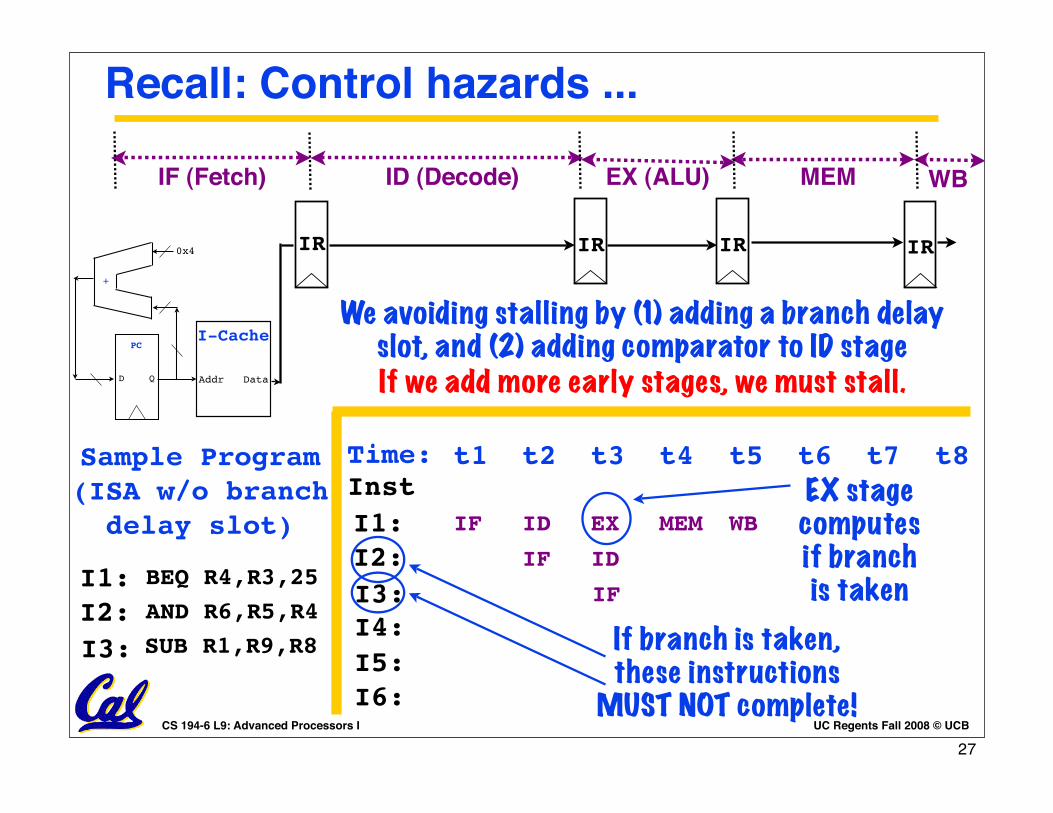
I1:I2:I3:I4:I5:
t1 t2 t3 t4 t5 t6 t7 t8Time:Inst
I6:
Recall: Control hazards ...
D
PC
Q
+
0x4
Addr Data
Instr
Mem
IR IR
IF (Fetch) ID (Decode) EX (ALU)
IR IR
MEM WB
BEQ R4,R3,25
SUB R1,R9,R8AND R6,R5,R4
I1:I2:I3:
Sample Program(ISA w/o branch delay slot) IF ID
IF
EX
ID
IF
MEM WBEX stage computes if branch is taken
If branch is taken, these instructions
MUST NOT complete!
We avoiding stalling by (1) adding a branch delay slot, and (2) adding comparator to ID stageIf we add more early stages, we must stall.
I-Cache
27

UC Regents Fall 2008 © UCBCS 194-6 L9: Advanced Processors I
I1:I2:I3:I4:I5:
t1 t2 t3 t4 t5 t6 t7 t8Time:Inst
I6:
D
PC
Q
+
0x4
Addr Data
Instr
Mem
IR IR
IF (Fetch) ID (Decode) EX (ALU)
IR IR
MEM WB
IF ID
IF
EX
ID
IF
MEM WBEX stage computes if branch is taken
If we predicted incorrectly, these instructions MUST
NOT complete!
We update the PC based on the outputs of the branch predictor. If it is perfect, pipe stays full!Dynamic Predictors: a cache of branch history
I-Cache
Solution: Branch prediction ...
A control instr?
Taken or Not Taken?
If taken, where to? What PC?
Branch Predictor
Predictions
28

UC Regents Fall 2008 © UCBCS 194-6 L9: Advanced Processors I
Branch predictors cache branch history
0b0110[...]01001000 BNEZ R1 Loop
Update BHT/BTB for next
time,oncetrue
behavior known
“Taken” or“Not Taken”
Branch History Table
(BHT)
2 bits
target addressBranch Target Buffer (BTB)
“Taken” Address
PC + 4 + Loop
28-bit address tag
0b0110[...]0100
Address of BNEZ instruction
=
Hit
28 bits
80-90%
accurate
Must check prediction, kill instruction if needed.29

UC Regents Fall 2008 © UCBCS 194-6 L9: Advanced Processors I
Simple (”2-bit”) Branch History Table Entry
D Q
Prediction for next branch. (1 = take, 0 = not take)
Initialize to 0.
BNE R4,R0,loopSUBI R4,R4,-1loop:
This branch taken 10 times, then not taken once (end of loop). The next time we enter the loop, we would like to predict “take” the first time through.
ADDI R4,R0,11
We do not change the prediction the first time it is incorrect. Why?
D Q
Was last prediction correct? (1 = yes, 0 = no) Initialize to 1.
Set to 1 if prediction bit was correct.Set to 0 if prediction bit was incorrect.
Set to 1 if prediction bit flips.
Flip bit if prediction is not correct and “last
predict correct” bit is 0.
After we “check” prediction ...
30

UC Regents Fall 2008 © UCBCS 194-6 L9: Advanced Processors I
Spatial enhancements: many BHTs ...0b0110[...]01001000 BNEZ R1 Loop
(BHT00) (BHT01) (BHT10) (BHT11)
“Taken” or “Not Taken”
Branch History Tables
Adaptive function of history, state
Detects patterns in:
if (x < 12) [...]if (x < 6) [...]
code.
Yeh and Patt,1992.
95% accurate
BHT00/01/10/11 code the last four branches in the instruction stream
31

UC Regents Fall 2008 © UCBCS 194-6 L9: Advanced Processors I
Hardware limits to superpipelining?
!"#$%&'()*#+&$,-
./#+&$,-0(,#$.&"12-13 456756887 9,#$.&"1):$';-"(',<
!"#$%&'(&)*+
8
=8
68
78
48
>8
?8
@8
A8
B8
=88
A> A? A@ AA AB B8 B= B6 B7 B4 B> B? B@ BA BB 88 8= 86 87 84 8>
'$,-/)7A?
'$,-/)4A?
'$,-/)C-$,'3D
'$,-/)C-$,'3D)6
'$,-/)C-$,'3D)7
'$,-/)C-$,'3D)4
'$,-/)',#$'3D
E/CF#)6=8?4
E/CF#)6==?4
E/CF#)6=6?4
9C#"%
93C-"9C#"%
9C#"%?4
G'C(
HI)IE
I&J-")IK
EGL)M?
EGL)M@
EGL)NA?O?4
Thanks to Francois Labonte, Stanford
FO4Delays
Historicallimit:about12
CPU Clock Periods1985-2005
MIPS 20005 stages
Pentium 420 stages
Pentium Pro10 stages
Power wall:Intel Core Duo has 14 stagesFO4: How many fanout-of-4 inverter
delays in the clock period.
32

UC Regents Fall 2008 © UCBCS 194-6 L9: Advanced Processors I
Superscalar
Basic Idea: Improve CPI by issuing several instructions per cycle.
33

UC Regents Fall 2008 © UCBCS 194-6 L3: Single-Cycle CPU
Recall VLIW: Super-sized Instructions
Example: All instructions are 64-bit. Each instruction consists of two 32-bit MIPS instructions, that execute in parallel.
opcode rs rt rd functshamt
opcode rs rt rd functshamt
Syntax: ADD $8 $9 $10 Semantics:$8 = $9 + $10
Syntax: ADD $7 $8 $9 Semantics:$7 = $8 + $9
A 64-bit VLIW instruction
But what if we can’t change ISA execution semantics ?
34

UC Regents Fall 2008 © UCBCS 194-6 L9: Advanced Processors I
IR IR
IF (Fetch) ID (Decode) EX (ALU)
IR IR
MEM WB
IR IR
IF (Fetch) ID (Decode) EX (ALU)
IR IR
MEM WB
rd1
RegFile
rd2
WE1
wd1
rs1
rs2
ws1
WE2
rd3
rd4
rs3
rs4
wd2
ws2
A
B
A
B
32A
L
U
32
32
op
Y
32A
L
U
32
32
op
Y
R
R
Superscalar R machine
Addr
DataInstrMem
64
32PC and
Sequencer
Instruction Issue Logic
35

UC Regents Fall 2008 © UCBCS 194-6 L9: Advanced Processors I
IR IR
IF (Fetch) ID (Decode) EX (ALU)
IR IR
MEM WB
IR IR
ID (Decode) EX (ALU)
IR IR
MEM WB
rd1
RegFile
rd2
WE1
wd1
rs1
rs2
ws1
WE2
rd3
rd4
rs3
rs4
wd2
ws2
A
B
A
B
32A
L
U
32
32
op
Y
32A
L
U
32
32
op
Y
R
R
Sustaining Dual Instr Issues
(no forwarding)
ADD R21,R20,R19ADD R24,R23,R22
ADD R21,R20,R19
ADD R24,R23,R22
ADD R15,R14,R13ADD R18,R17,R16
ADD R15,R14,R13
ADD R18,R17,R16
ADD R27,R26,R25ADD R30,R29,R28
ADD R27
ADD R30
ADD R9,R8,R7
ADD R12,R11,R10
ADD R9,R8,R7ADD R12,R11,R10
ADD R8,R0,R0ADD R11,R0,R0
It’s rarely this good ...
36
UC Regents Fall 2008 © UCBCS 194-6 L9: Advanced Processors I
IR IR
IF (Fetch) ID (Decode) EX (ALU)
IR IR
MEM WB
IR IR
ID (Decode) EX (ALU)
IR IR
MEM WB
rd1
RegFile
rd2
WE1
wd1
rs1
rs2
ws1
WE2
rd3
rd4
rs3
rs4
wd2
ws2
A
B
A
B
32A
L
U
32
32
op
Y
32A
L
U
32
32
op
Y
R
R
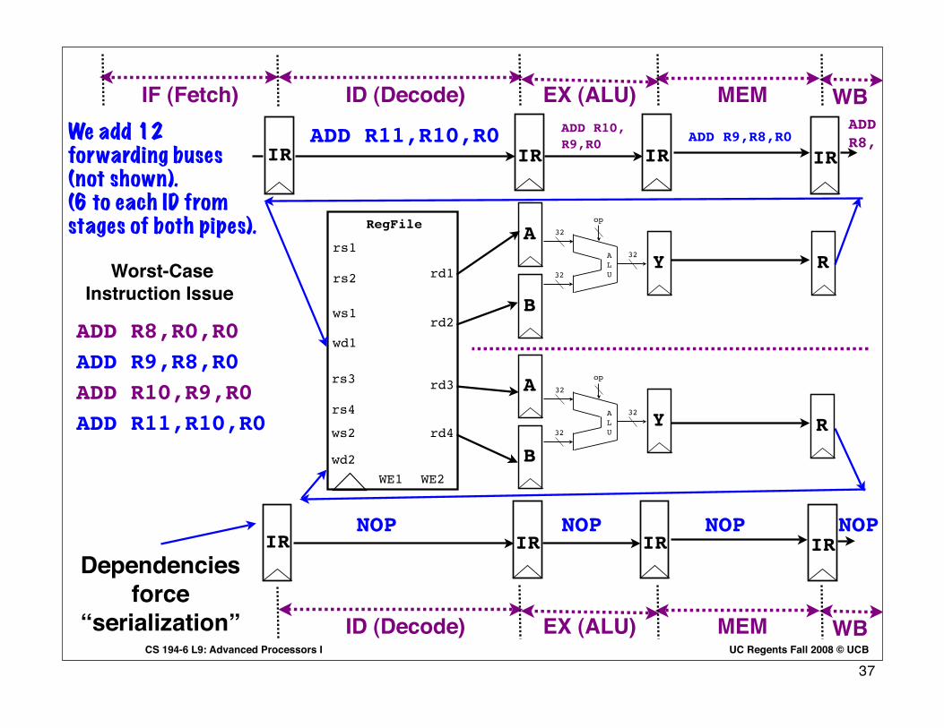
Worst-Case Instruction Issue
NOP
ADD R8,
ADD R8,R0,R0
ADD R9,R8,R0
ADD R9,R8,R0
ADD R10,R9,R0
ADD R10,R9,R0
ADD R11,R10,R0
ADD R11,R10,R0
NOP NOP NOP
Dependencies force
“serialization”
We add 12 forwarding buses (not shown).(6 to each ID from stages of both pipes).
37

UC Regents Fall 2008 © UCBCS 194-6 L9: Advanced Processors I
!"#$%&
!"#$%
&'"()*+,-*.,,/
012.3-*4++556
789($:;9*<9:$*=)'"'($%":#$:(#
>8#?
>8#?
.*(?( .*(?(
+(?( +(?( +(?(
!"##$
%&%'#&(')
%*+,&*##$
%&%'#&(')
789($:;9*89:$#*)'@%*:9$%"9'A*B:B%A:9%*"%C:#$%"#
!"" ;B%"'9D#*'"%*A'$()%D*E)%9*'9*:9#$"8($:;9*
%9$%"#*'*F89($:;9*89:$*
!"" :9B8$#*$;*'*F89($:;9*89:$*G%1C1-*"%C:#$%"*F:A%H
('9*()'9C%*D8":9C*'*A;9C*A'$%9(?*;B%"'$:;9
'((%B$
'((%B$
!"#$%
&'"()*+,-*.,,/
012.3-*4++550
&8A$:BA%*789($:;9*<9:$#
I7 IJ KL
M4< &%N
7'DD
7N8A
7D:@
I##8%
OPQR#
7PQR#
Example: Superscalar MIPS. Fetches 2 instructions at a time. If first integer and second floating point, issue in same cycle
Superscalar: A simple example ...
Integer instruction FP instruction
LD F0,0(R1) LD F6,-8(R1) LD F10,-16(R1) ADDD F4,F0,F2 LD F14,-24(R1) ADDD F8,F6,F2 LD F18,-32(R1) ADDD F12,F10,F2 SD 0(R1),F4 ADDD F16,F14,F2 SD -8(R1),F8 ADDD F20,F18,F2 SD -16(R1),F12 SD -24(R1),F16
Two issuesper cycle
One issueper cycle
Why is the control for
this CPU not so hard to do?
38

UC Regents Fall 2008 © UCBCS 194-6 L9: Advanced Processors I
!"#$%&
!"#$%
&'"()*+,-*.,,/
012.3-*4++556
789($:;9*<9:$*=)'"'($%":#$:(#
>8#?
>8#?
.*(?( .*(?(
+(?( +(?( +(?(
!"##$
%&%'#&(')
%*+,&*##$
%&%'#&(')
789($:;9*89:$#*)'@%*:9$%"9'A*B:B%A:9%*"%C:#$%"#
!"" ;B%"'9D#*'"%*A'$()%D*E)%9*'9*:9#$"8($:;9*
%9$%"#*'*F89($:;9*89:$*
!"" :9B8$#*$;*'*F89($:;9*89:$*G%1C1-*"%C:#$%"*F:A%H
('9*()'9C%*D8":9C*'*A;9C*A'$%9(?*;B%"'$:;9
'((%B$
'((%B$
!"#$%
&'"()*+,-*.,,/
012.3-*4++550
&8A$:BA%*789($:;9*<9:$#
I7 IJ KL
M4< &%N
7'DD
7N8A
7D:@
I##8%
OPQR#
7PQR#
Three instructions potentially affected by a single cycle of load delay, as FP register loads done in the “integer” pipeline).
Superscalar: Visualizing the pipeline
Type Pipe Stages Int. instruction IF ID EX MEM WB FP instruction IF ID EX MEM WB Int. instruction IF ID EX MEM WB FP instruction IF ID EX MEM WB Int. instruction IF ID EX MEM WB FP instruction IF ID EX MEM WB
39

UC Regents Fall 2008 © UCBCS 194-6 L9: Advanced Processors I
Limitations of “lockstep” superscalarGets 0.5 CPI only for a 50/50 float/int mix with no hazards. For games/media, this may be OK.Extending scheme to speed up general apps (Microsoft Office, ...) is complicated.
If one accepts building a complicated machine, there are better ways to do it.
The Power5 scans fetched instructions forbranches (BP stage), and if it finds a branch,predicts the branch direction using threebranch history tables shared by the twothreads. Two of the BHTs use bimodal andpath-correlated branch prediction mecha-nisms to predict branch directions.6,7 Thethird BHT predicts which of these predictionmechanisms is more likely to predict the cor-
rect direction.7 If the fetched instructions con-tain multiple branches, the BP stage can pre-dict all the branches at the same time. Inaddition to predicting direction, the Power5also predicts the target of a taken branch inthe current cycle’s eight-instruction group. Inthe PowerPC architecture, the processor cancalculate the target of most branches from theinstruction’s address and offset value. For
43MARCH–APRIL 2004
MP ISS RF EA DC WB Xfer
MP ISS RF EX WB Xfer
MP ISS RF EX WB Xfer
MP ISS RF
XferF6
Group formation andinstruction decode
Instruction fetch
Branch redirects
Interrupts and flushes
WB
Fmt
D1 D2 D3 Xfer GD
BPICCP
D0
IF
Branchpipeline
Load/storepipeline
Fixed-pointpipeline
Floating-point pipeline
Out-of-order processing
Figure 3. Power5 instruction pipeline (IF = instruction fetch, IC = instruction cache, BP = branch predict, D0 = decode stage0, Xfer = transfer, GD = group dispatch, MP = mapping, ISS = instruction issue, RF = register file read, EX = execute, EA =compute address, DC = data caches, F6 = six-cycle floating-point execution pipe, Fmt = data format, WB = write back, andCP = group commit).
Shared by two threads Thread 0 resources Thread 1 resources
LSU0FXU0
LSU1
FXU1
FPU0
FPU1
BXU
CRL
Dynamicinstructionselection
Threadpriority
Group formationInstruction decode
Dispatch
Shared-register
mappers
Readshared-
register files
Sharedissue
queues
Sharedexecution
units
Alternate
Branch prediction
Instructioncache
Instructiontranslation
Programcounter
Branchhistorytables
Returnstack
Targetcache
DataCache
DataTranslation
L2cache
Datacache
Datatranslation
Instructionbuffer 0
Instructionbuffer 1
Writeshared-
register files
Groupcompletion
Storequeue
Figure 4. Power5 instruction data flow (BXU = branch execution unit and CRL = condition register logical execution unit).
Next Monday:DynamicScheduling
40

UC Regents Fall 2008 © UCBCS 194-6 L9: Advanced Processors I
Virtual Memory
41

UC Regents Fall 2008 © UCBCS 194-6 L9: Advanced Processors I
The Limits of Physical Addressing
CPU Memory
A0-A31 A0-A31
D0-D31 D0-D31
“Physical addresses” of memory locations
Data
All programs share one address space: The physical address space
No way to prevent a program from accessing any machine resource
Machine language programs must beaware of the machine organization
Where we are ...
42

UC Regents Fall 2008 © UCBCS 194-6 L9: Advanced Processors I
Apple II: A physically-addressed machine
Apple ][ (1977)
Steve WozniakSteve
Jobs
CPU: 1000 ns DRAM: 400 ns
43

UC Regents Fall 2008 © UCBCS 194-6 L9: Advanced Processors I
Apple II: A physically addressed machine Apple ][ (1977)
44

UC Regents Fall 2008 © UCBCS 194-6 L9: Advanced Processors I
The Limits of Physical Addressing
CPU Memory
A0-A31 A0-A31
D0-D31 D0-D31
“Physical addresses” of memory locations
Data
All programs share one address space: The physical address space
No way to prevent a program from accessing any machine resource
Machine language programs must beaware of the machine organization
Programming the Apple ][ ...
45

UC Regents Fall 2008 © UCBCS 194-6 L9: Advanced Processors I
Solution: Add a Layer of Indirection
CPU Memory
A0-A31 A0-A31
D0-D31 D0-D31
Data
User programs run in an standardizedvirtual address space
Address Translation hardware managed by the operating system (OS)
maps virtual address to physical memory
“Physical Addresses”
AddressTranslation
Virtual Physical
“Virtual Addresses”
Hardware supports “modern” OS features:Protection, Translation, Sharing
46

UC Regents Fall 2008 © UCBCS 194-6 L9: Advanced Processors I
MIPS R4000: Address Space ModelProcess A
AddressError
2 GB
0
231
232
- 1
Process B
AddressError
2 GB
0
231
232
- 1
Process A and B have independent address spaces
ASID = 12 ASID = 13
ASID = Address Space Identifier
When Process A writes its address 9, it writes to a different physical memory location than
Process B’s address 9
May only be accessed by kernel/supervisor
To let Process A and B share memory, OS maps parts of
ASID 12 and ASID 13 to the same physical memory locations.
All address spacesuse a standard memory map
Still works (slowly!) if a process accesses more virtual memory than the machine has physical memory
47

UC Regents Fall 2008 © UCBCS 194-6 L9: Advanced Processors I
MIPS R4000: Who’s Running on the CPU?System Control Registers
Chapter 4
80 MIPS R4000 Microprocessor User' s Manual
4.3 System Control Coprocessor
The System Control Coprocessor (CP0) is implemented as an integral part
of the CPU, and supports memory management, address translation,
exception handling, and other privileged operations. CP0 contains the
registers shown in Figure 4-7 plus a 48-entry TLB. The sections that follow
describe how the processor uses the memory management-related
registers†.
Each CP0 register has a unique number that identifies it; this number is
referred to as the register number. For instance, the Page Mask register is
register number 5.
Figure 4-7 CP0 Registers and the TLB
† For a description of CP0 data dependencies and hazards, please see Appendix F.
EntryLo02*
EntryHi
Page Mask
Index
Random
Wired
Count
47
0
BadVAddr
TLB
(“Safe” entries)
(See Random Register,
PRId
0127
8*
15*
Compare
11*
Config
16*
LLAddr
17*
WatchLo
18*
WatchHi
19*
TagLo
28*TagHi
29*
contents of TLB Wired)ECC
26*
*Register number
Used with exception
processing. SeeUsed with memory
Chapter 5 for details.
EntryLo0
2*
3*
EntryLo1
EntryHi
10*
5*Page Mask
Index
0*
Random1*
Wired6*
ErrorEPC
30*
Context
4*
Status
12*Cause
13*
EPC14*
management system.
CacheErr
27*
XContext
20*
9*
User cannot write supervisor/kernel bits. Supervisor cannot write kernel bit.
User cannot change address translation configuration
Status (12): Indicatesuser, supervisor, or
kernel mode
EntryLo0 (2): 8-bit ASID field codes virtualaddress space ID.
48
UC Regents Fall 2008 © UCBCS 194-6 L9: Advanced Processors I
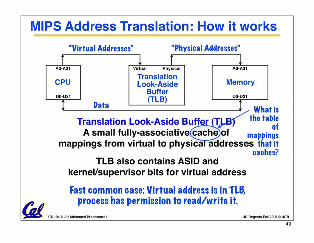
MIPS Address Translation: How it works“Physical Addresses”
CPU Memory
A0-A31 A0-A31
D0-D31 D0-D31
Data
TLB also contains ASID andkernel/supervisor bits for virtual address
Virtual Physical
“Virtual Addresses”
TranslationLook-Aside
Buffer(TLB)
Translation Look-Aside Buffer (TLB)A small fully-associative cache of
mappings from virtual to physical addresses
Fast common case: Virtual address is in TLB, process has permission to read/write it.
What is the table
ofmappings
that it caches?
49

UC Regents Fall 2008 © UCBCS 194-6 L9: Advanced Processors I
Page tables encode virtual address spaces
A machine usually supports
pages of a few sizes
(MIPS R4000):
MIPS R4000 Microprocessor User' s Manual 87
Memory Management
EntryLo0 (2), and EntryLo1 (3) Registers
The EntryLo register consists of two registers that have identical formats:
• EntryLo0 is used for even virtual pages.
• EntryLo1 is used for odd virtual pages.
The EntryLo0 and EntryLo1 registers are read / write registers. They hold
the physical page frame number (PFN) of the TLB entry for even and odd
pages, respectively, when performing TLB read and write operations.
Figure 4-10 shows the format of these registers.
PageMask Register (5)
The PageMask register is a read / write register used for read ing from or
writing to the TLB; it holds a comparison mask that sets the variable page
size for each TLB entry, as shown in Table 4-9.
TLB read and write operations use this register as either a source or a
destination; when virtual addresses are presented for translation into
physical address, the corresponding bits in the TLB identify which virtual
address bits among bits 24:13 are used in the comparison. When the Mask
field is not one of the values shown in Table 4-9, the operation of the TLB
is undefined .
Table 4-9 Mask Field Values for Page Sizes
Page SizeBi t
24 23 22 21 20 19 18 17 16 15 14 13
4 Kbytes 0 0 0 0 0 0 0 0 0 0 0 0
16 Kbytes 0 0 0 0 0 0 0 0 0 0 1 1
64 Kbytes 0 0 0 0 0 0 0 0 1 1 1 1
256 Kbytes 0 0 0 0 0 0 1 1 1 1 1 1
1 Mbyte 0 0 0 0 1 1 1 1 1 1 1 1
4 Mbytes 0 0 1 1 1 1 1 1 1 1 1 1
16 Mbytes 1 1 1 1 1 1 1 1 1 1 1 1
PhysicalMemory Space
A valid page table entry codes physical memory “frame” address for the page
A virtual address spaceis divided into blocks
of memory called pagesframeframe
frame
frame
A page table is indexed by a virtual address
virtual address
Page Table(One per ASID)
OS manages the page table for each ASID
50
UC Regents Fall 2008 © UCBCS 194-6 L9: Advanced Processors I
!"#$"%!&'()*+,-./0*1%%!
(+#21*"*345.6789.:;****
<=:1#>1#
CPU Registers100s Bytes<10s ns
CacheK Bytes10-100 ns$.01-.001/bit
Main MemoryM Bytes100ns-1us$.01-.001
DiskG Bytesms10 - 10 cents
-3 -4
CapacityAccess TimeCost
Tapeinfinitesec-min10-6
Registers
Cache
Memory
Disk
Tape
?/@7->*A,=-6/B@
)C8:D@
E60=@
F.C=@
StagingXfer Unit
prog./compiler1-8 bytes
cache cntl8-128 bytes
OS512-4K bytes
user/operatorMbytes
',,=-*<=G=C
<89=-*<=G=C
H6@7=-
<6-0=-
Recall: Levels of the Memory Hierarchy
!"#$"%!&'()*+,-./0*1%%!
(+#21*"*345.6789.:;****
<=:1#>11
IVirtual memory => treat memory as a cache for the diskITerminology: blocks in this cache are called “Pages”JTypical size of a page: 1K — 8K
IPage table maps virtual page numbers to physical framesJ“PTE” = Page Table Entry
Physical Address Space
Virtual Address Space
What is virtual memory?
Virtual Address
Page Table
./B=K
./78
,60=
765C=
E60=*L65C=
)6@=M=0
VAccessRights PA
V page no. offset10
765C=*C8:67=B
./*,NO@.:6C
P=P8-O
P page no. offset
10
Physical Address
!"#$"%!&'()*+,-./0*1%%!
(+#21*"*345.6789.:;****
<=:1#>1Q
Three Advantages of Virtual Memory
ITranslation:JProgram can be given consistent view of memory, even
though physical memory is scrambled
JMakes multithreading reasonable (now used a lot!)
JOnly the most important part of program (“Working Set”) must be in physical memory.
JContiguous structures (like stacks) use only as much physical memory as necessary yet still grow later.
IProtection:JDifferent threads (or processes) protected from each other.
JDifferent pages can be given special behaviorR(Read Only, Invisible to user programs, etc).
JKernel data protected from User programs
JVery important for protection from malicious programs=> Far more “viruses” under Microsoft Windows
ISharing:JCan map same physical page to multiple users
(“Shared memory”)!"#$"%!&'()*+,-./0*1%%!
(+#21*"*345.6789.:;****
<=:1#>1!
What is the size of information blocks that are transferred from secondary to main storage (M)? ⇒ page size(Contrast with physical block size on disk, I.e. sector size)
Which region of M is to hold the new block ⇒ placement policy
How do we find a page when we look for it? ⇒ block identification
Block of information brought into M, and M is full, then some region of M must be released to make room for the new block ⇒ replacement policy
What do we do on a write? ⇒ write policy
Missing item fetched from secondary memory only on the occurrence of a fault ⇒ demand load policy
pages
reg
cachemem disk
frame
Issues in Virtual Memory System Design
V=0 pages either reside on disk or
have not yet been allocated.
OS handles V=0“Page fault”
In this example,physical and virtual
pages must be the same size!
The TLB caches page table entries
TLB
Page Table
2
0
1
3
virtual address
page off
2frame page
250
physical address
page off
TLB caches page table
entries.
MIPS handles TLB misses in software (random replacement). Other
machines use hardware.
for ASID
Physicalframe
address
51
UC Regents Fall 2008 © UCBCS 194-6 L9: Advanced Processors I
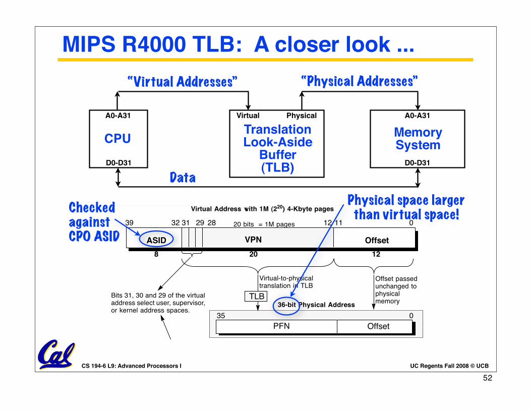
MIPS R4000 TLB: A closer look ...“Physical Addresses”
CPU MemorySystem
A0-A31 A0-A31
D0-D31 D0-D31
Data
TranslationLook-Aside
Buffer(TLB)
Virtual Physical
“Virtual Addresses”
MIPS R4000 Microprocessor User' s Manual 65
Memory Management
32-bit Mode Address Translation
Figure 4-2 shows the virtual-to-physical-address translation of a 32-bit
mode address.
• The top portion of Figure 4-2 shows a virtual add ress w ith a
12-bit, or 4-Kbyte, page size, labelled Offset. The remaining 20
bits of the add ress represent the VPN, and index the 1M-entry
page table.
• The bottom portion of Figure 4-2 shows a virtual add ress w ith
a 24-bit, or 16-Mbyte, page size, labelled Offset. The remaining
8 bits of the add ress represent the VPN, and index the 256-
entry page table.
Figure 4-2 32-bit Mode Virtual Address Translation
28 11 0
20 12
2931
VPN Offset
3239
ASID
8
Virtual Address with 1M (220) 4-Kbyte pages
23 0
8 24
Offset
39
Virtual Address with 256 (28)16-Mbyte pages
8 bits = 256 pages
20 bits = 1M pages 12
ASID
8
28 293132
VPN
24
Virtual-to-physicaltranslation in TLB
Bits 31, 30 and 29 of the virtualaddress select user, supervisor,or kernel address spaces.
Offset passedunchanged tophysicalmemory
Virtual-to-physicaltranslation in TLB
TLB
TLB
35 0
PFN Offset
Offset passedunchanged tophysicalmemory
36-bit Physical Address
Physical space larger than virtual space!Checked
againstCPO ASID
52

UC Regents Fall 2008 © UCBCS 194-6 L9: Advanced Processors I
Can TLB and caching be overlapped?
Index Byte Select
Valid
Cache Block
Cache Block
Cache Tags Cache Data
Data out
Virtual Page Number Page Offset
TranslationLook-Aside
Buffer(TLB)
Virtual
Physical
=
Hit
Cache Tag
This works, but ...
Q. What is the downside?
A. Inflexibility. VPN size locked to cache tag size.
53
UC Regents Fall 2008 © UCBCS 194-6 L9: Advanced Processors I
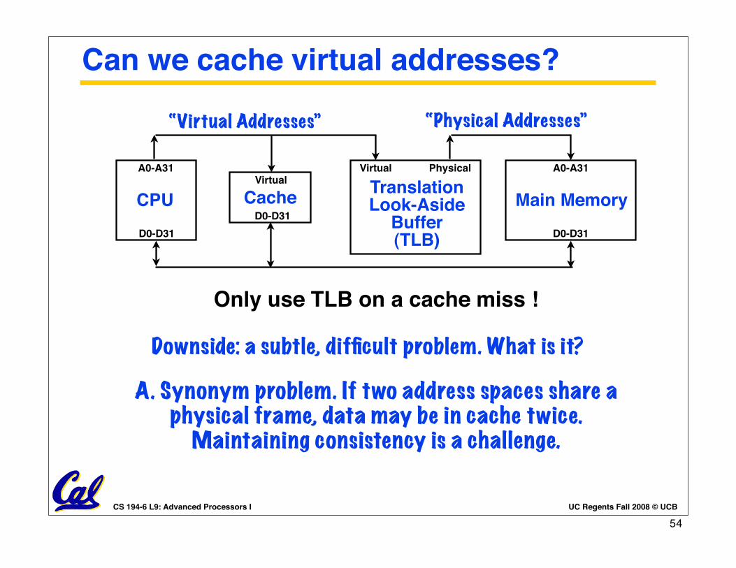
Can we cache virtual addresses?
“Physical Addresses”
CPU Main Memory
A0-A31 A0-A31
D0-D31 D0-D31
Only use TLB on a cache miss !
TranslationLook-Aside
Buffer(TLB)
Virtual Physical
“Virtual Addresses”
A. Synonym problem. If two address spaces share a physical frame, data may be in cache twice.
Maintaining consistency is a challenge.
CacheVirtual
D0-D31
Downside: a subtle, difficult problem. What is it?
54

UC Regents Fall 2008 © UCBCS 194-6 L9: Advanced Processors I
Virtualization
55

UC Regents Fall 2008 © UCBCS 194-6 L9: Advanced Processors I
Parallels: Running Windows on a MacLike software emulating a PC, but different. Use an Intel-based Mac, runs on top of OS X. Uses hardware support to create a fast virtual PC that boots Windows. +++ Reasonable performance.
Virtual CPU runs 33% slower than running on physical CPU.
2 GB physical memory for a 512 MB virtual PC to run w/o disk swaps.
Source: http://www.atpm.com/12.10/parallels.shtml56
UC Regents Fall 2008 © UCBCS 194-6 L9: Advanced Processors I
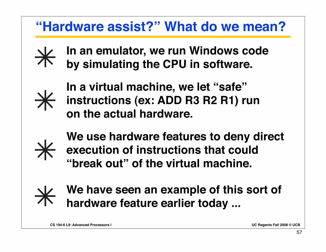
“Hardware assist?” What do we mean?In an emulator, we run Windows code by simulating the CPU in software.
In a virtual machine, we let “safe” instructions (ex: ADD R3 R2 R1) run on the actual hardware.
We use hardware features to deny direct execution of instructions that could “break out” of the virtual machine.
We have seen an example of this sort of hardware feature earlier today ...
57

UC Regents Fall 2008 © UCBCS 194-6 L9: Advanced Processors I
!"#$"%!&'()*+,-./0*1%%!
(+#21*"*345.6789.:;****
<=:1#>1#
CPU Registers100s Bytes<10s ns
CacheK Bytes10-100 ns$.01-.001/bit
Main MemoryM Bytes100ns-1us$.01-.001
DiskG Bytesms10 - 10 cents
-3 -4
CapacityAccess TimeCost
Tapeinfinitesec-min10-6
Registers
Cache
Memory
Disk
Tape
?/@7->*A,=-6/B@
)C8:D@
E60=@
F.C=@
StagingXfer Unit
prog./compiler1-8 bytes
cache cntl8-128 bytes
OS512-4K bytes
user/operatorMbytes
',,=-*<=G=C
<89=-*<=G=C
H6@7=-
<6-0=-
Recall: Levels of the Memory Hierarchy
!"#$"%!&'()*+,-./0*1%%!
(+#21*"*345.6789.:;****
<=:1#>11
IVirtual memory => treat memory as a cache for the diskITerminology: blocks in this cache are called “Pages”JTypical size of a page: 1K — 8K
IPage table maps virtual page numbers to physical framesJ“PTE” = Page Table Entry
Physical Address Space
Virtual Address Space
What is virtual memory?
Virtual Address
Page Table
./B=K
./78
,60=
765C=
E60=*L65C=
)6@=M=0
VAccessRights PA
V page no. offset10
765C=*C8:67=B
./*,NO@.:6C
P=P8-O
P page no. offset
10
Physical Address
!"#$"%!&'()*+,-./0*1%%!
(+#21*"*345.6789.:;****
<=:1#>1Q
Three Advantages of Virtual Memory
ITranslation:JProgram can be given consistent view of memory, even
though physical memory is scrambled
JMakes multithreading reasonable (now used a lot!)
JOnly the most important part of program (“Working Set”) must be in physical memory.
JContiguous structures (like stacks) use only as much physical memory as necessary yet still grow later.
IProtection:JDifferent threads (or processes) protected from each other.
JDifferent pages can be given special behaviorR(Read Only, Invisible to user programs, etc).
JKernel data protected from User programs
JVery important for protection from malicious programs=> Far more “viruses” under Microsoft Windows
ISharing:JCan map same physical page to multiple users
(“Shared memory”)!"#$"%!&'()*+,-./0*1%%!
(+#21*"*345.6789.:;****
<=:1#>1!
What is the size of information blocks that are transferred from secondary to main storage (M)? ⇒ page size(Contrast with physical block size on disk, I.e. sector size)
Which region of M is to hold the new block ⇒ placement policy
How do we find a page when we look for it? ⇒ block identification
Block of information brought into M, and M is full, then some region of M must be released to make room for the new block ⇒ replacement policy
What do we do on a write? ⇒ write policy
Missing item fetched from secondary memory only on the occurrence of a fault ⇒ demand load policy
pages
reg
cachemem disk
frame
Issues in Virtual Memory System Design
V=0 pages either reside on disk or
have not yet been allocated.
OS handles V=0“Page fault”
In this example,physical and virtual
pages must be the same size!
Recall: A LW that misses TLB launches a program!
TLB
Page Table
2
0
1
3
virtual address
page off
2frame page
250
physical address
page off
TLB caches page table
entries.
MIPS handles TLB misses in software (random replacement). Other
machines use hardware.
for ASID
Physicalframe
address
58

UC Regents Fall 2008 © UCBCS 194-6 L9: Advanced Processors I
General Mechanism: Instruction TrapConceptually, we set CPU up to rewrite “unsafe” instructions with a function call.
CPU rewrite instructions??? We have already done this for pipelining ....
ADD R4,R3,R2
UNSAFE
AND R2,R2,R1
ADD R5,R2,R2
Sample Program What CPU DoesAND R2,R2,R1
ADD R4,R3,R2
JAL UNSAFE_STUB
NOP
ADD R5,R2,R2
59

UC Regents Fall 2006 © UCBCS 152 L18: Advanced Processors II
Recall: “Muxing in” NOPS to do stalls
rd1
RegFile
rd2
WEwd
rs1
rs2
ws
D
PC
Q
+
0x4
Addr Data
Instr
Mem
Ext
IR IR IR
B
A
M
Instr Fetch
Stage #1 Stage #2 Stage #3
Decode & Reg Fetch
ADD R4,R3,R2OR R5,R4,R2
Let ADD proceed to WB stage, so that R4 is written to regfile.
ADD R4,R3,R2OR R5,R4,R2
Sample programKeep executingOR instructionuntil R4 is ready.Until then, sendNOPS to IR 2/3.
Freeze PC and IR until stall is over.
New datapath hardware
(1) Mux into IR 2/3to feed in NOP.
(2) Write enable on PC and IR 1/2
60

UC Regents Fall 2008 © UCBCS 194-6 L9: Advanced Processors I
Conclusion: Superpipelining, Superscalar
The 5 stage pipeline: a starting point for performance enhancements, abuilding block for multiprocessing.
Superscalar: Multiple instructions at once. Programs must fit the issue rules. Adds complexity.
Superpipelining: Reduce critical pathby adding more pipeline stages. Hasthe potential to hurt the CPI.
61

UC Regents Fall 2008 © UCBCS 194-6 L9: Advanced Processors I
Next Monday:
This Friday: Project Meeting, 10 AM, 125 Cory
Final Presentation
Fri, Dec 5 62