cs485xx datasheet - statics.cirrus.com · dsp composer ™ gui development tool. processing chains...
TRANSCRIPT

CS485xx
CS485xx Family Data SheetFeatures
Cost-effective, High-performance 32-bit DSP
300,000,000 MAC/S (multiply accumulates per second)
Dual MAC cycles per clock
72-bit accumulators are the most accurate in the industry
24k x 32 SRAM, 2k blocks - assignable to data or program
Internal ROM contains a variety of configurable sound enhancement feature sets
8-channel internal DMA
Internal watch-dog DSP lock-up prevention
DSP Tool Set w/ Private Keys for Protecting Customer IP
Configurable Serial Audio Inputs/Outputs
Configurable for all input/output types
Maximum 32-bit @ 192 kHz
Supports 32-bit audio sample I/O between DSP chips
TDM input modes (multiple channels on same line)
192 kHz SPDIF transmitter
Multi-channel DSD direct stream digital SACD input
Supports Two Different Input Fs Sample Rates
Output can be master or slave
Dual processing path capability
Input supports dual domain slave clocking
Hardware assist time sampling for sample rate conversion
Integrated Clock Manager/PLL
Can operate from external crystal, external oscillator
Input Fs Auto Detection
Host & Boot via Serial Interface
Configurable GPIOs and External Interrupt Input
1.8V Core and a 3.3V I/O that is tolerant to 5V input
Low-power Mode
“Energy Star® Ready” in low-power mode, 268 µW in standby
Differentiating from the legacy Cirrus multi-standard, multi-channel decoders, this new CS485xx family is still based on the same high-performance 32-bit fixed point Digital Signal Processor core but instead is equipped with much less memory, tailoring it for more cost-effective applications associated with multi-channel and virtual-channel sound enhancements. Target applications are:
Digital Televisions
Multimedia Peripherals
iPod® Docking Stations
Automotive Head Units
Automotive Outboard Amplifiers
HD-DVD™ and Blu-ray Disc® DVD Receivers
PC Speakers
There are also a wide variety of licensable DSP codes available today as seen by the following examples:
Cirrus also has developed, or is developing their own royalty-free versions of popular features sets like Cirrus Bass Manager, Cirrus Dynamic Volume Leveler, Cirrus Original Multichannel Surround, Cirrus Virtual Speaker & Cirrus 3D-Audio.
The CS485xx family is programmed using the Cirrus proprietary DSP Composer™ GUI development tool. Processing chains may be designed using a drag-and-drop interface to place/utilize functional macro audio DSP primitives. The end result is a software image that is down-loaded to the DSP via serial host or serial boot modes.
See Section 6 for ordering information.
CS485xx Block Diagram
32-bitDSP
DMA
P X Y
SerialControl 1
12 Ch PCMAudio Out
GPIO Debug
Watchdog
TMR1
TMR2
PLL
S/PDIF
12 Ch. Audio In / 6 Ch. SACD In
Copyright Cirrus Logic, Inc. 2011(All Rights Reserved)http://www.cirrus.com DS734F5
OCT '11

Contacting Cirrus Logic Support For all product questions and inquiries, contact a Cirrus Logic Sales Representative. To find the one nearest you, go to www.cirrus.com.
IMPORTANT NOTICE
Cirrus Logic, Inc. and its subsidiaries (“Cirrus”) believe that the information contained in this document is accurate and reliable. However, the information is subject to changewithout notice and is provided “AS IS” without warranty of any kind (express or implied). Customers are advised to obtain the latest version of relevant information to verify,before placing orders, that information being relied on is current and complete. All products are sold subject to the terms and conditions of sale supplied at the time of orderacknowledgment, including those pertaining to warranty, indemnification, and limitation of liability. No responsibility is assumed by Cirrus for the use of this information,including use of this information as the basis for manufacture or sale of any items, or for infringement of patents or other rights of third parties. This document is the propertyof Cirrus and by furnishing this information, Cirrus grants no license, express or implied under any patents, mask work rights, copyrights, trademarks, trade secrets or otherintellectual property rights. Cirrus owns the copyrights associated with the information contained herein and gives consent for copies to be made of the information only foruse within your organization with respect to Cirrus integrated circuits or other products of Cirrus. This consent does not extend to other copying such as copying for generaldistribution, advertising or promotional purposes, or for creating any work for resale.
CERTAIN APPLICATIONS USING SEMICONDUCTOR PRODUCTS MAY INVOLVE POTENTIAL RISKS OF DEATH, PERSONAL INJURY, OR SEVERE PROPERTY ORENVIRONMENTAL DAMAGE (“CRITICAL APPLICATIONS”). CIRRUS PRODUCTS ARE NOT DESIGNED, AUTHORIZED OR WARRANTED FOR USE IN PRODUCTSSURGICALLY IMPLANTED INTO THE BODY, AUTOMOTIVE SAFETY OR SECURITY DEVICES, LIFE SUPPORT PRODUCTS OR OTHER CRITICAL APPLICATIONS.INCLUSION OF CIRRUS PRODUCTS IN SUCH APPLICATIONS IS UNDERSTOOD TO BE FULLY AT THE CUSTOMER’S RISK AND CIRRUS DISCLAIMS AND MAKESNO WARRANTY, EXPRESS, STATUTORY OR IMPLIED, INCLUDING THE IMPLIED WARRANTIES OF MERCHANTABILITY AND FITNESS FOR PARTICULARPURPOSE, WITH REGARD TO ANY CIRRUS PRODUCT THAT IS USED IN SUCH A MANNER. IF THE CUSTOMER OR CUSTOMER’S CUSTOMER USES OR PERMITSTHE USE OF CIRRUS PRODUCTS IN CRITICAL APPLICATIONS, CUSTOMER AGREES, BY SUCH USE, TO FULLY INDEMNIFY CIRRUS, ITS OFFICERS, DIRECTORS,EMPLOYEES, DISTRIBUTORS AND OTHER AGENTS FROM ANY AND ALL LIABILITY, INCLUDING ATTORNEYS’ FEES AND COSTS, THAT MAY RESULT FROM ORARISE IN CONNECTION WITH THESE USES.
Cirrus Logic, Cirrus, and the Cirrus Logic logo designs, DSP Composer, and Cirrus Framework are trademarks of Cirrus Logic, Inc. All other brand and product names in thisdocument may be trademarks or service marks of their respective owners.
Dolby, Dolby Digitaol, Dolby Headphone, Virtual Speaker, and Pro Logic are registered trademarks of Dolby Laboratories, Inc. Supply of an implementation of DolbyTechnology does not convey a license nor imply a right under any patent, or any other industrial or Intellectual Property Right of Dolby Laboratories, to use the Implementationin any finished end-user or ready-to-use final product. It is hereby notified that a license for such use is required from Dolby Laboratories.
DTS and DTS Neo:6 are registered trademarks of Digital Theater Systems, Inc. It is hereby notified that a third-party license from DTS is necessary to distribute software ofDTS in any finished end-user or ready-to-use final product.
SRS, Circle Surround and Trusurround XT are registered trademarks of SRS Labs, Inc. Circle Surround II is a trademark of SRS Labs, Inc. The Circle Surround technologyis incorporated under license from SRS Labs, Inc. The Circle Surround technology rights incorporated in the CS485xx are owned by SRS Labs, a U.S. Corporation andlicensed to Cirrus Logic, Inc. Purchaser of CS485xx must sign a license for use of the chip and display of the SRS Labs trademarks. Any products incorporating the CS485xxmust be sent to SRS Labs for review. The Circle Surround technology is protected under US and foreign patents issued and/or pending. Circle Surround, SRS and (O) symbolare trademarks of SRS Labs, Inc. in the United States and selected foreign countries. Neither the purchase of the CS485xx, nor the corresponding sale of audio enhancementequipment conveys the right to sell commercialized recordings made with any SRS technology/solution. SRS Labs requires all set makers to comply with all rules andregulations as outlined in the SRS Trademark Usage Manual.
SPI is a trademark of Motorola, Inc.
I²C is a trademark of Philips Semiconductor.
iPod is a registered trademark of Apple Computer, Inc.
HD DVD is a trademark of DVD Format/Logo Licensing Corporation.
Blu-Ray Disc is a registered trademark of SONY KABUSHIKI KAISHA CORPORATION.
Energy Star is a registered trademark of the Environmental Protection Agency, a federal agency of the United States government.
DS734F5 2

TABLE OF CONTENTS1 Documentation Strategy ........................................................................................................................................... 1-52 Overview ..................................................................................................................................................................... 2-5
2.1 Licensing ............................................................................................................................................................ 2-53 Code Overlays ............................................................................................................................................................ 3-64 Hardware Functional Description ............................................................................................................................ 4-7
4.1 DSP Core ........................................................................................................................................................... 4-74.1.1 DSP Memory ............................................................................................................................................. 4-74.1.2 DMA Controller .......................................................................................................................................... 4-7
4.2 On-chip DSP Peripherals ................................................................................................................................... 4-74.2.1 Digital Audio Input Port (DAI) .................................................................................................................... 4-74.2.2 Digital Audio Output Port (DAO) ................................................................................................................ 4-84.2.3 Serial Control Port (I2C™ or SPI™) ............................................................................................................ 4-84.2.4 GPIO ......................................................................................................................................................... 4-84.2.5 PLL-based Clock Generator ...................................................................................................................... 4-84.2.6 Hardware Watchdog Timer ....................................................................................................................... 4-8
4.3 DSP I/O Description ........................................................................................................................................... 4-84.3.1 Multiplexed Pins ........................................................................................................................................ 4-84.3.2 Termination Requirements ........................................................................................................................ 4-84.3.3 Pads .......................................................................................................................................................... 4-9
4.4 Application Code Security .................................................................................................................................. 4-95 Characteristics and Specifications .......................................................................................................................... 5-9
5.1 Absolute Maximum Ratings ................................................................................................................................ 5-95.2 Recommended Operations Conditions ............................................................................................................... 5-95.3 Digital DC Characteristics ................................................................................................................................... 5-95.4 Power Supply Characteristics ........................................................................................................................... 5-105.5 Thermal Data (48-pin LQFP) ............................................................................................................................ 5-105.6 Switching Characteristics—RESET .................................................................................................................. 5-115.7 Switching Characteristics—XTI ........................................................................................................................ 5-115.8 Switching Characteristics—Internal Clock ........................................................................................................ 5-115.9 Switching Characteristics—Serial Control Port–SPI Slave Mode ..................................................................... 5-125.10 Switching Characteristics—Serial Control Port–SPI Master Mode ................................................................. 5-135.11 Switching Characteristics—Serial Control Port–I2C Slave Mode ................................................................... 5-135.12 Switching Characteristics—Serial Control Port–I2C Master Mode ................................................................. 5-145.13 Switching Characteristics—Digital Audio Slave Input Port ............................................................................. 5-155.14 Switching Characteristics—DSD Slave Input Port .......................................................................................... 5-155.15 Switching Characteristics—Digital Audio Output (DAO) Port ......................................................................... 5-16
6 Ordering Information ............................................................................................................................................... 6-187 Environmental, Manufacturing, and Handling Information ................................................................................. 7-188 Device Pinout Diagrams .......................................................................................................................................... 8-19
8.1 CS48520, 48-pin LQFP Pinout Diagram .......................................................................................................... 8-198.2 CS48540, 48-pin LQFP Pinout Diagram .......................................................................................................... 8-208.3 CS48560, 48-pin LQFP Pinout Diagram .......................................................................................................... 8-21
9 Package Mechanical Drawings ............................................................................................................................... 9-229.1 48-pin LQFP Package Drawing ........................................................................................................................ 9-22
10 Revision History .................................................................................................................................................. 10-23
3 DS734F5
LIST OF FIGURESFigure 5-1. RESET Timing ...................................................................................................................................... 5-11Figure 5-2. XTI Timing............................................................................................................................................. 5-11Figure 5-3. Serial Control Port–SPI Slave Mode Timing ......................................................................................... 5-12Figure 5-4. Serial Control Port–SPI Master Mode Timing ....................................................................................... 5-13Figure 5-5. Serial Control Port–I2C Slave Mode Timing.......................................................................................... 5-14Figure 5-6. Serial Control Port–I2C Master Mode Timing........................................................................................ 5-15Figure 5-7. Digital Audio Input (DAI) Port Timing Diagram...................................................................................... 5-15Figure 5-8. Direct Stream Digital–Serial Audio Input Timing ................................................................................... 5-15Figure 5-9. Digital Audio Output Port Timing, Master Mode.................................................................................... 5-17Figure 5-10. Digital Audio Output Timing, Slave Mode (Relationship LRCLK to SCLK) ......................................... 5-17Figure 8-1. CS48520, 48-pin LQFP Pinout.............................................................................................................. 8-19Figure 8-2. CS48540, 48-pin LQFP Pinout.............................................................................................................. 8-20Figure 8-3. CS48560, 48-pin LQFP......................................................................................................................... 8-21Figure 9-1. 48-pin LQFP Package Drawing............................................................................................................. 8-22
LIST OF TABLESTable 1-1. CS485xx Family Related Documentation................................................................................................. 1-5Table 3-1. Device and Firmware Selection Guide ..................................................................................................... 3-6Table 5-1. Master Mode (Output A1 Mode)............................................................................................................. 5-16Table 5-2. Slave Mode (Output A0 Mode)............................................................................................................... 5-17Table 6-1. Ordering Information .............................................................................................................................. 6-18Table 7-1. Environmental, Manufacturing, and Handling Information ..................................................................... 7-18
4 DS734F5

1 Documentation Strategy
1 Documentation Strategy
The CS485xx Family Data Sheet describes the CS485xx family of multichannel audio processors. This document should be used in conjunction with the following documents when evaluating or designing a system around the CS485xx family of processors.
The scope of the CS485xx Family Data Sheet is primarily the hardware specifications of the CS485xx family of devices. This includes hardware functionality, characteristic data, pinout, and packaging information.
The intended audience for the CS485xx Family Data Sheet is the system PCB designer, MCU programmer, and the quality control engineer.
2 Overview
The CS485xx DSP Family is designed to provide high-performance post-processing and mixing of digital audio. The dual clock domain provided on the PCM inputs allows for the mixing of audio streams with different sampling frequencies. The low-power standby preserves battery life for applications which are always on, but not necessarily processing audio, such as automotive audio systems.
There are three devices comprising the CS485xx family. The CS48520, CS48540 and CS48560 are differentiated by the number of inputs and outputs available. All DSPs support dual input clock domains and dual audio processing paths. All DSPs are available in a 48-pin QFP package. Refer to Table 3-1 for the input, output, firmware features of each device.
2.1 Licensing
Licenses are required for all of the third party audio processing algorithms listed in Section 3. Contact your local Cirrus Logic Sales representative for more information.
Table 1-1. CS485xx Family Related Documentation
Document Name Description
CS485xx Family Data Sheet This documentCS485xx Family Hardware User’s Manual Includes detailed system design information including Typical Connection Diagrams,
Boot-Procedures, Pin Descriptions, etc.AN298–CS485xx Family Firmware User’s Manual Includes detailed firmware design information including signal processing flow
diagrams and control API informationDSP Composer User’s Manual Includes detailed configuration and usage information for the GUI development tool.
5 DS734F5
3 Code Overlays
3 Code Overlays
The suite of software available for the CS485xx family consists of an operating system (OS) and a library of overlays. The overlays have been divided into three main groups called Matrix-processors, Virtualizer-processors, and Post-processors. All software components are defined below:
1. OS/Kernel—Encompasses all non-audio processing tasks, including loading data from external memory, processing host messages, calling audio-processing subroutines, error concealment, etc.
2. Matrix-processor—Any Module that performs a matrix decode on PCM data to produce more output channels than input channels (2n channels). Examples are Dolby ProLogic IIx and DTS Neo:6. Generally speaking, these modules increase the number of valid channels in the audio I/O buffer.
3. Virtualizer-processor—Any module that encodes PCM data into fewer output channels than input channels (n2 channels) with the effect of providing “phantom” speakers to represent the physical audio channels that were eliminated. Examples are Dolby Headphone® and Dolby Virtual Speaker®. Generally speaking, these modules reduce the number of valid channels in the audio I/O buffer.
4. Post-processors—Any module that processes audio I/O buffer PCM data in-place after the matrix- or virtualizer-processors. Examples are bass management, audio manager, tone control, EQ, delay, customer-specific effects, etc.
The bulk of each overlay is stored in ROM within the CS485xx, but a small image is required to configure the overlays and boot the DSP. This small image can either be stored in an external serial FLASH/EEPROM, or downloaded via a host controller through the SPI™/I2C™ serial port.
The overlay structure reduces the time required to reconfigure the DSP when a processing change is requested. Each overlay can be reloaded independently without disturbing the other overlays. For example, when a new matrix-processor is selected, the OS, virtualizer-, and post-processors do not need to be reloaded — only the new matrix-processor (the same is true for the other overlays).
Table 3-1 lists the firmware available based on device selection. Refer AN298, CS485xx Firmware User’s Manual for the latest listing of application codes and Cirrus Framework™ modules available.
Table 3-1. Device and Firmware Selection Guide
Device Suggested Application Channel Count Input/Output Package
CS48520-CQZ Digital TV, portable audio docking station, portable DVD, DVD mini/receiver, multimedia PC speakers
Up to 4-channel in/4-channel out 48-pin QFP
CS48540-CQZCS48540-DQZ
CS48520 features plus 8-channel car audio, DVD receiver Up to 8-channel in/8-channel out 48-pin QFP
CS48560-CQZCS48560-DQZ
CS48540 features plus 12-channel car audio, high-end digital TV, dual source/dual zone SACD
Up to 12-channel in/12-channel out 48-pin QFP
6 DS734F5

4 Hardware Functional Description
4 Hardware Functional Description
4.1 DSP Core
The CS485xx family DSPs are single-core DSP with separate X and Y data and P code memory spaces. The DSP core is a high-performance, 32-bit, user-programmable, fixed-point DSP that is capable of performing two multiply-and-accumulate (MAC) operations per clock cycle. The DSP core has eight 72-bit accumulators, four X- and four Y-data registers, and 12 index registers.
The DSP core is coupled to a flexible DMA engine. The DMA engine can move data between peripherals such as the serial control port (SCP), digital audio input (DAI) and digital audio output (DAO), or any DSP core memory, all without the intervention of the DSP. The DMA engine off loads data move instructions from the DSP core, leaving more MIPS available for signal processing instructions.
CS485xx family functionality is controlled by application codes that are stored in on-board ROM or downloaded to the CS485xx from a host controller or external serial FLASH/EEPROM.
Users can develop their applications using DSP Composer to create the processing chain and then compile the image into a series of commands that are sent to the CS485xx through the SCP. The processing application can either load modules (matrix-processors, virtualizers, post-processors) from the DSPs on-board ROM, or custom firmware can be downloaded through the SCP.
The CS485xx is suitable for a variety of audio post-processing applications such as automotive head-ends, automotive amplifiers, and boom boxes.
4.1.1 DSP Memory
The DSP core has its own on-chip data and program RAM and ROM and does not require external memory for post-processing applications.
The Y-RAM and P-RAM share a single block of memory that can be configured to make Y and P equal in size, or more memory can be allocated for Y-RAM in 2kword blocks.
4.1.2 DMA Controller
The powerful 8-channel DMA controller can move data between 8 on-chip resources. Each resource has its own arbiter: X, Y, and P RAMs/ROMs and the peripheral bus. Modulo and linear addressing modes are supported, with flexible start address and increment controls. The service intervals for each DMA channel, as well as up to 6 interrupt events, are programmable.
4.2 On-chip DSP Peripherals
4.2.1 Digital Audio Input Port (DAI)
Each version of the CS485xx supports a different number of input channels. Refer to Table 3-1 for more details.
The DAI port supports a wide variety of data input formats at sample rates (Fs) as high as 192 kHz. The port is capable of accepting PCM or DSD formats. Up to 32-bit word lengths are supported. DSD is supported and internally converted to PCM before processing. The DAI also supports a time division multiplexed (TDM) one-line data mode, that packs PCM audio on a single data line (the total number possible depends on the ratio of SCLK to LRCLK and the version of chip. For example on the CS48520 only 4 ch of PCM are supported in one line mode and on the CS48560 up to 8 channels are supported.).
The port has two independent slave-only clock domains. Each data input can be independently assigned to a clock domain. The sample rate of the input clock domains can be determined automatically by the DSP, off-loading the task of monitoring the SPDIF receiver from the host. A time-stamping feature allows the input data to be sample-rate converted via software.
7 DS734F5
4.3 DSP I/O Description
4.2.2 Digital Audio Output Port (DAO)
Each version of the CS485xx supports a different number of output channels. Refer to Table 3-1 for more details.
DAO port supports PCM resolutions of up to 32-bits. The port supports sample rates (Fs) as high as 192 kHz. The port can be configured as an independent clock domain mastered by the DSP, or as a clock slave if an external MCLK or SCLK/LRCLK source is available. One of the serial audio pins can be re-configured as a S/PDIF transmitter that drives a biphase encoded S/PDIF signal (data with embedded clock on a single line).
The DAO also supports a time division multiplexed (TDM) one-line data mode, that packs multiple channels of PCM audio on a single data line.
4.2.3 Serial Control Port (I2C™ or SPI™)
The on-chip serial control port is capable of operating as master or slave in either SPI™ or I2C™ modes. Master/Slave operation is chosen by mode select pins when the CS485xx comes out of Reset. The serial clock pin can support frequencies as high as 25 MHz in SPI mode (SPI clock speed must always be ≤ (Fdclk/2)). The CS485xx serial control port also includes a pin for flow control of the communications interface (SCP_BSY) and a pin to indicate when the DSP has a message for the host (SCP_IRQ).
4.2.4 GPIO
Many of the CS485xx peripheral pins are multiplexed with GPIO. Each GPIO can be configured as an output, an input, or an input with interrupt. Each input-pin interrupt can be configured as rising edge, falling edge, active-low, or active-high.
4.2.5 PLL-based Clock Generator
The low-jitter PLL generates integer or fractional multiples of a reference frequency which are used to clock the DSP core and peripherals. Through a second PLL divider chain, a dependent clock domain can be output on the DAO port for driving audio converters. The CS485xx defaults to running from the external reference frequency and is switched to use the PLL output after overlays have been loaded and configured, either through master boot from an external FLASH or through host control. A built-in crystal oscillator circuit with a buffered output is provided. The buffered output frequency ratio is selectable between 1:1 (default) or 2:1.
4.2.6 Hardware Watchdog Timer
The CS485xx has an integrated watchdog timer that acts as a “health” monitor for the DSP. The watchdog timer must be reset by the DSP before the counter expires, or the entire chip is reset. This peripheral ensures that the CS485xx will reset itself in the event of a temporary system failure. In stand-alone mode (that is, no host MCU), the DSP will reboot from external FLASH. In slave mode (that is, host MCU present) a GPIO will be used to signal the host that the watchdog has expired and the DSP should be rebooted and re-configured.
4.3 DSP I/O Description
4.3.1 Multiplexed Pins
Many of the CS485xx family pins are multi-functional. For details on pin functionality, refer to the CS485xx Hardware User’s Manual.
4.3.2 Termination Requirements
Open-drain pins on the CS485xx must be pulled high for proper operation. Refer to the CS485xx Hardware User’s Manual to identify which pins are open-drain and what value of pull-up resistor is required for proper operation.
Mode select pins in the CS485xx family are used to select the boot mode upon the rising edge from reset. A detailed explanation of termination requirements for each communication mode select pin can be found in the CS485xx Hardware User’s Manual.
8 DS734F5

4.4 Application Code Security
4.3.3 Pads
The CS485xx I/Os operate from the 3.3 V supply and are 5 V tolerant.
4.4 Application Code Security
The external program code may be encrypted by the programmer to protect any intellectual property it may contain. A secret, customer-specific key is used to encrypt the program code that is to be stored external to the device. Contact your local Cirrus representative for details.
5 Characteristics and Specifications
Note: All data sheet minimum and maximum timing parameters are guaranteed over the rated voltage and temperature. All data sheet typical parameters are measured under the following conditions: T = 25° C, CL = 20 pF, VDD = VDDA = 1.8 V, VDDIO = 3.3 V, GNDD = GNDIO = GNDA = 0 V.
5.1 Absolute Maximum Ratings
(GNDD = GNDIO = GNDA = 0 V; all voltages with respect to 0 V)
WARNING: Operation at or beyond these limits may result in permanent damage to the device. Normal operation is notguaranteed at these extremes.
5.2 Recommended Operations Conditions
(GNDD = GNDIO = GNDA = 0 V; all voltages with respect to 0 V)
Note: It is recommended that the 3.3 V IO supply come up ahead of or simultaneously with the 1.8 V core supply.
5.3 Digital DC Characteristics
(Measurements performed under static conditions.)
Parameter Symbol Min Max Unit
DC power supplies: Core supply VDD –0.3 2.0 V
PLL supply VDDA –0.3 3.6 V
I/O supply VDDIO –0.3 3.6 V
|VDDA–VDDIO| — — 0.3 V
Input pin current, any pin except supplies Iin — ±10 mA
Input voltage on PLL_REF_RES Vfilt –0.3 3.6 V
Input voltage on I/O pins Vinio –0.3 5.0 V
Storage temperature Tstg –65 150 °C
Parameter Symbol Min Typ Max Unit
DC power supplies: Core supply VDD 1.71 1.8 1.89 V
PLL supply VDDA 3.13 3.3 3.46 V
I/O supply VDDIO 3.13 3.3 3.46 V
|VDDA–VDDIO| — — 0 — V
Ambient operating temperature TA — — — °C
–CQZ — 0 — +70 —
–DQZ — –40 — +85 —
9 DS734F5

5.4 Power Supply Characteristics
5.4 Power Supply Characteristics
(Measurements performed under operating conditions)
5.5 Thermal Data (48-pin LQFP)
Parameter Symbol Min Typ Max Unit
High-level input voltage VIH 2.0 — — V
Low-level input voltage, except XTI VIL — — 0.8 V
Low-level input voltage, XTI VILXTI — — 0.6 V
Input hysteresis Vhys — 0.4 — V
High-level output voltage (IO = –2 mA), except XTI VOH VDDIO*0.9 — — V
Low-level output voltage (IO = 2 mA), except XTI VOL — — VDDIO*0.1 V
Input leakage XTI ILXTI — — 5 µA
Input leakage current (all digital pins with internal pull-up resistors enabled) ILEAK — — 70 µA
Parameter Min Typ Max Unit
Operational Power Supply Current:
VDD: Core and I/O operating1
1.Dependent on application firmware and DSP clock speed.
— 203 — mA
VDDA: PLL operating — 8 — mA
VDDIO: With most ports operating — 27 — mA
Total Operational Power Dissipation: — 480 — mW
Standby Power Supply Current:
VDD: Core and I/O not clocked — 100 — µA
VDDA: PLL halted — 1 — µA
VDDIO: All connected I/O pins 3-stated by other ICs in system — 50 — µA
Total Standby Power Dissipation — 348 — µW
Parameter Symbol Min Typ Max Unit
Junction Temperature Tj — — 125 °C
Thermal Resistance (Junction to Ambient)
Two-layer board1
Four-layer board2
1.Two-layer board is specified as a 76 mm X 114 mm, 1.6 mm thick FR-4 material with 1 oz. copper covering 20% of the top and bottom layers.2.Four-layer board is specified as a 76 mm X 114 mm, 1.6 mm thick FR-4 material with 1 oz. copper covering 20% of the top and bottom layers and 0.5
oz. copper covering 90 % of the internal power plane and ground plane layers.
θja — 63.5 — °C/Watt
— 54 —
Thermal Resistance (Junction to Top of Package)
Two-layer board3
Four-layer board4
3.To calculate the die temperature for a given power dissipation
Tj = Ambient Temperature + [(Power Dissipation in Watts)*θja]
4.To calculate the case temperature for a given power dissipation
Tc = Tj – [(Power Dissipation in Watts)*ψ jt]
ψ jt — 0.70 — °C/Watt
— 0.64 —
10 DS734F5

5.6 Switching Characteristics—RESET
5.6 Switching Characteristics—RESET
Figure 5-1. RESET Timing
5.7 Switching Characteristics—XTI
Figure 5-2. XTI Timing
5.8 Switching Characteristics—Internal Clock
Parameter Symbol Min Max Unit
RESET# minimum pulse width low Trstl 1 — ms
All bidirectional pins high-Z after RESET# low Trst2z — 100 ns
Configuration pins setup before RESET# high Trstsu 50 — ns
Configuration pins hold after RESET# high Trsthld 20 — ns
Parameter Symbol Min Max Unit
External Crystal operating frequency1
1.Part characterized with the following crystal frequency values: 11.2896, 12.288, 18.432, 24.576, & 27 MH.z
Fxtal 11.2896 27 MHz
XTI period Tclki 33.3 100 ns
XTI high time Tclkih 13.3 — ns
XTI low time Tclkil 13.3 — ns
External Crystal Load Capacitance (parallel resonant)2
2.CL refers to the total load capacitance as specified by the crystal manufacturer. Crystals that require a CL outside this range should be avoided. The crystal oscillator circuit design should follow the crystal manufacturer’s recommendation for load capacitor selection.
CL 10 18 pF
External Crystal Equivalent Series Resistance ESR — 50 Ω
Parameter Symbol Min Max Unit
Internal DCLK frequency1 Fdclk — — MHz
CS4852x-CQZCS4854x-CQZCS4856x-CQZCS4854x-DQZCS4856x-DQZ
Fxtal
Fxtal
Fxtal
Fxtal
Fxtal
150150150150150
RESET#
Trst2z
Trstl
Trstsu Trsthld
HS[3:0]
All BidirectionalPins
t clkih t clkil
Tclki
XTI
11 DS734F5

5.9 Switching Characteristics—Serial Control Port–SPI Slave Mode
5.9 Switching Characteristics—Serial Control Port–SPI Slave Mode
Figure 5-3. Serial Control Port–SPI Slave Mode Timing
Internal DCLK period1 DCLKP — — ns
CS4852x-CQZCS4854x-CQZCS4856x-CQZCS4854x-DQZCS4856x-DQZ
6.76.76.76.76.7
1/Fxtal
1/Fxtal
1/Fxtal
1/Fxtal
1/Fxtal
1.After initial power-on reset, Fdclk = Fxtal. After initial kick-start commands, the PLL is locked to max Fdclk and remains locked until the next power-on reset.
Parameter Symbol Min Typical Max Units
SCP_CLK frequency1
1.The specification fspisck indicates the maximum speed of the hardware. The system designer should be aware that the actual maximum speed of the communication port may be limited by the firmware application. Flow control using the SCP_BSY# pin should be implemented to prevent overflow of the input data buffer. At boot the maximum speed is Fxtal/3.
fspisck — — 25 MHz
SCP_CS# falling to SCP_CLK rising tspicss 24 — — ns
SCP_CLK low time tspickl 20 — — ns
SCP_CLK high time tspickh 20 — — ns
Setup time SCP_MOSI input tspidsu 5 — — ns
Hold time SCP_MOSI input tspidh 5 — — ns
SCP_CLK low to SCP_MISO output valid tspidov — — 11 ns
SCP_CLK falling to SCP_IRQ# rising tspiirqh — — 20 ns
SCP_CS# rising to SCP_IRQ# falling tspiirql 0 — — ns
SCP_CLK low to SCP_CS# rising tspicsh 24 — — ns
SCP_CS# rising to SCP_MISO output high-Z tspicsdz — 20 — ns
SCP_CLK rising to SCP_BSY# falling tspicbsyl — 3*DCLKP+20 — ns
Parameter Symbol Min Max Unit
SCP_BSY#
SCP_CS#
SCP_CLK
SCP_MOSI
SCP_MISO
SCP_IRQ#
0 1 2 6 7 0 5 6 7
tspicss
tspickl
tspickh
tspidsu
tspidh tspidov
A6 A5 A0 R/W MSB LSB
MSB LSB
tspicsh
tspibsyl
tspiirqltspiirqh
fspisck
tspicsdz
12 DS734F5
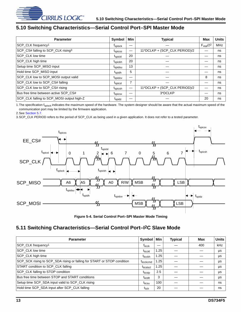
5.10 Switching Characteristics—Serial Control Port–SPI Master Mode
5.10 Switching Characteristics—Serial Control Port–SPI Master Mode
Figure 5-4. Serial Control Port–SPI Master Mode Timing
5.11 Switching Characteristics—Serial Control Port–I2C Slave Mode
Parameter Symbol Min Typical Max Units
SCP_CLK frequency1
1.The specification fspisck indicates the maximum speed of the hardware. The system designer should be aware that the actual maximum speed of the communication port may be limited by the firmware application.
fspisck — — Fxtal/22
2.See Section 5.7.
MHz
SCP_CS# falling to SCP_CLK rising3
3.SCP_CLK PERIOD refers to the period of SCP_CLK as being used in a given application. It does not refer to a tested parameter.
tspicss — 11*DCLKP + (SCP_CLK PERIOD)/2 — ns
SCP_CLK low time tspickl 20 — — ns
SCP_CLK high time tspickh 20 — — ns
Setup time SCP_MISO input tspidsu 13 — — ns
Hold time SCP_MISO input tspidh 5 — — ns
SCP_CLK low to SCP_MOSI output valid tspidov — — 8 ns
SCP_CLK low to SCP_CS# falling tspicsl 7 — — ns
SCP_CLK low to SCP_CS# rising tspicsh — 11*DCLKP + (SCP_CLK PERIOD)/2 — ns
Bus free time between active SCP_CS# tspicsx — 3*DCLKP — ns
SCP_CLK falling to SCP_MOSI output high-Z tspidz — — 20 ns
Parameter Symbol Min Typical Max Units
SCP_CLK frequency1 fiicck — — 400 kHz
SCP_CLK low time tiicckl 1.25 — — µs
SCP_CLK high time tiicckh 1.25 — — µs
SCP_SCK rising to SCP_SDA rising or falling for START or STOP condition tiicckcmd 1.25 — — µs
START condition to SCP_CLK falling tiicstscl 1.25 — — µs
SCP_CLK falling to STOP condition tiicstp 2.5 — — µs
Bus free time between STOP and START conditions tiicbft 3 — — µs
Setup time SCP_SDA input valid to SCP_CLK rising tiicsu 100 — — ns
Hold time SCP_SDA input after SCP_CLK falling tiich 20 — — ns
EE_CS#
SCP_CLK
SCP_MISO
SCP_MOSI
0 1 2 6 7 0 5 6 7
tspicss
tspickl
tspickh
tspidsu
tspidh tspidov
A6 A5 A0 R/W MSB LSB
MSB LSB
tspicsh
tspicsx
fspisck
tspidz
tspicsl
13 DS734F5

5.12 Switching Characteristics—Serial Control Port–I2C Master Mode
Figure 5-5. Serial Control Port–I2C Slave Mode Timing
5.12 Switching Characteristics—Serial Control Port–I2C Master Mode
SCP_CLK low to SCP_SDA out valid tiicdov — — 18 ns
SCP_CLK falling to SCP_IRQ# rising tiicirqh — — 3*DCLKP + 40 ns
NAK condition to SCP_IRQ# low tiicirql — 3*DCLKP + 20 — ns
SCP_CLK rising to SCB_BSY# low tiicbsyl — 3*DCLKP + 20 — ns
1.The specification fiicck indicates the maximum speed of the hardware. The system designer should be aware that the actual maximum speed of the communication port may be limited by the firmware application. Flow control using the SCP_BSY# pin should be implemented to prevent overflow of the input data buffer.
Parameter Symbol Min Max Units
SCP_CLK frequency1
1.The specification fiicck indicates the maximum speed of the hardware. The system designer should be aware that the actual maximum speed of the communication port may be limited by the firmware application.
fiicck — 400 kHz
SCP_CLK low time tiicckl 1.25 — µs
SCP_CLK high time tiicckh 1.25 — µs
SCP_SCK rising to SCP_SDA rising or falling for START or STOP condition tiicckcmd 1.25 — µs
START condition to SCP_CLK falling tiicstscl 1.25 — µs
SCP_CLK falling to STOP condition tiicstp 2.5 — µs
Bus free time between STOP and START conditions tiicbft 3 — µs
Setup time SCP_SDA input valid to SCP_CLK rising tiicsu 100 — ns
Hold time SCP_SDA input after SCP_CLK falling tiich 20 — ns
SCP_CLK low to SCP_SDA out valid tiicdov — 18 ns
Parameter Symbol Min Typical Max Units
SCP_BSY#
SCP_CLK
SCP_SDA
SCP_IRQ#
0 1 6 7 8 0 1 7
tiicckl
tiicckh
tiicsu tiich
A6 A0 R/W ACK LSB
tiicirqh tiicirql
8
ACKMSB
tiicstp
6
tiiccbsyl
tiicdov tiicbfttiicstscl
tiicckcmd
fiicck
tiicckcmdtiicftiicr
14 DS734F5

5.13 Switching Characteristics—Digital Audio Slave Input Port
Figure 5-6. Serial Control Port–I2C Master Mode Timing
5.13 Switching Characteristics—Digital Audio Slave Input Port
Figure 5-7. Digital Audio Input (DAI) Port Timing Diagram
5.14 Switching Characteristics—DSD Slave Input Port
Figure 5-8. Direct Stream Digital–Serial Audio Input Timing
Parameter Symbol Min Max Unit
DAI_SCLK period Tdaiclkp 40 — ns
DAI_SCLK duty cycle — 45 55 %
Setup time DAI_DATAn tdaidsu 10 — ns
Hold time DAI_DATAn tdaidh 5 — ns
Parameter Symbol Min Typ Max Unit
DSD_SCLK Pulse Width Low tsclkl 78 — — ns
DSD_SCLK Pulse Width High tsclkh 78 — — ns
DSD_SCLK Frequency (64x Oversampled) — 1.024 — 3.2 MHz
DSD_A/B valid to DSD_SCLK rising setup time tsdlrs 20 — — ns
DSD_SCLK rising to DSD_A or DSD_B hold time tsdh 20 — — ns
SCP_CLK
SCP_SDA
0 1 6 7 8 0 1 7
tiicckl
tiicckh
tiicsu tiich
A6 A0 R/W ACK LSB
8
ACKMSB
tiicstp
6
tiicdov tiicbfttiicstscl
tiicckcmd
fiicck
tiicckcmdtiicftiicr
DAI_SCLK
DAI_DATAn
tdaidhtdaidsu
15 DS734F5

5.15 Switching Characteristics—Digital Audio Output (DAO) Port
5.15 Switching Characteristics—Digital Audio Output (DAO) Port
Figure 5-9. Digital Audio Output Port Timing, Master Mode
Parameter Symbol Min Max Unit
DAO_MCLK period Tdaomclk 40 — ns
DAO_MCLK duty cycle — 45 55 %
DAO_SCLK period for Master or Slave mode1
1.Master mode timing specifications are characterized, not production tested.
Tdaosclk 40 — ns
DAO_SCLK duty cycle for Master or Slave mode1 — 40 60 %
Table 5-1. Master Mode (Output A1 Mode)1,2
1.Master mode timing specifications are characterized, not production tested.2.Master mode is defined as the CS48xx driving both DAO_SCLK, DAO_LRCLK. When MCLK is an input, it is divided to produce DAO_SCLK, DAO_
LRCLK.
Parameter Symbol Min Max Unit
DAO_SCLK delay from DAO_MCLK rising edge, DAO_MCLK as an input tdaomsck — 19 nsDAO_LRCLK delay from DAO_SCLK transition, respectively3
3.This timing parameter is defined from the non-active edge of DAO_SCLK. The active edge of DAO_SCLK is the point at which the data is valid.
tdaomstlr — 8 nsDAO_SCLK delay from DAO_LRCLK transition, respectively3 tdaomlrts — 8 nsDAO1_DATA[3:0], DAO2_DATA[1:0] delay from DAO_SCLK transition3 tdaomdv — 10 ns
DAO_MCLK
DAO_SCLK
DAO_LRCLK
DAOn_DATAn
tdaomclk
tdaomsck
tdaomstlr
Note: In these diagrams, Falling edge is the inactive edge of DAO_SCLK.
16 DS734F5

5.15 Switching Characteristics—Digital Audio Output (DAO) Port
Figure 5-10. Digital Audio Output Timing, Slave Mode (Relationship LRCLK to SCLK)
Table 5-2. Slave Mode (Output A0 Mode)1
1.Slave mode is defined as DAO_SCLK, DAO_LRCLK driven by an external source.
Parameter Symbol Min Max Unit
DAO_SCLK active edge to DAO_LRCLK transition tdaosstlr 10 — nsDAO_LRCLK transition to DAO_SCLK active edge tdaoslrts 10 — nsDAO_Dx delay from DAO_SCLK inactive edge tdaosdv — 11 ns
DAO_SCLK
DAO_LRCLK
DAOn_DATAn
tdaosstlr
tdaosclk
DAO_SCLK
DAO_LRCLK
tdaoslrts
tdaosdv
tdaosclk
Note: In these diagrams, Falling edge is the inactive edge of DAO_SCLK.
17 DS734F5

6 Ordering Information
6 Ordering Information
The CS485xx family part number is CS485NI-XYZR where:
• N–Product Number Variant
• I–ROM ID Number
• X–Product Grade
• Y–Package Type
• Z–Lead (Pb) Free
• R–Tape and Reel Packaging
Note: Contact the factory for availability of the automotive grade package.
7 Environmental, Manufacturing, and Handling Information
Table 6-1. Ordering Information
Part No. Grade Temp. Range Package
CS48520-CQZ Commercial 0 to +70° C 48-pin LQFPCS48540-CQZ Commercial 0 to +70° CCS48540-DQZ Automotive –40 to +85° CCS48560-CQZ Commercial 0 to +70° CCS48560-DQZ Automotive –40 to +85° C
Table 7-1. Environmental, Manufacturing, and Handling Information
Model Number Peak Reflow Temp MSL Rating1
1.MSL (Moisture Sensitivity Level) as specified by IPC/JEDEC J-STD-020.
Max Floor Life
CS48520-CQZ 260° C 3 7 daysCS48540-CQZCS48540-DQZCS48560-CQZCS48560-DQZ
18 DS734F5
8 Device Pinout Diagrams
8 Device Pinout Diagrams
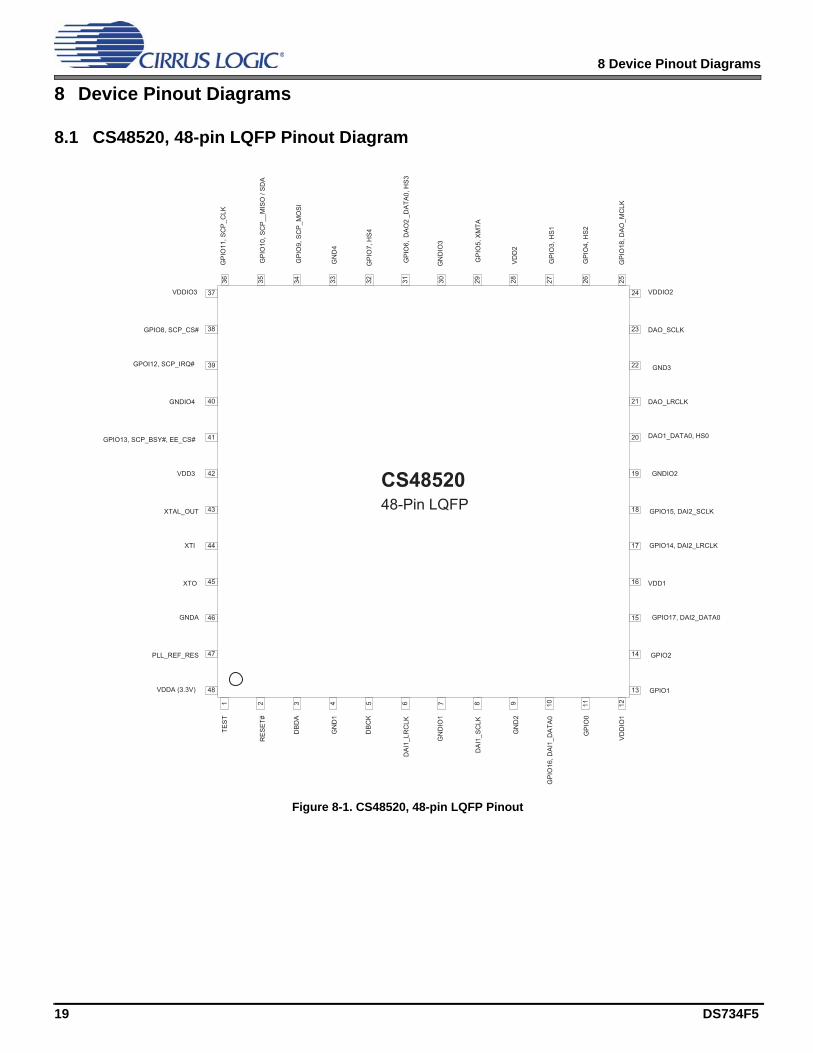
8.1 CS48520, 48-pin LQFP Pinout Diagram
Figure 8-1. CS48520, 48-pin LQFP Pinout
XTO
XTI
GNDA
PLL_REF_RES
VDDA (3.3V) GPIO1
GPIO2
GP
IO16
,DA
I1_D
ATA
0
GP
IO0
38
40
41
42
43
45
46
GPIO13, SCP_BSY#, EE_CS#
GPOI12, SCP_IRQ#
GP
IO10
,SC
P__
MIS
O/S
DA
GP
IO9,
SC
P_M
OS
I
GP
IO11
,SC
P_C
LK
35 33 31 30 28 26 25
GN
D4
GNDIO4
VDD3
GND3
VDDIO3
GN
DIO
3
23
22
21
19
17
15
1
GP
IO5,
XM
TA
GP
IO3,
HS
1
DAO1_DATA0, HS0
DAO_LRCLKD
AI1
_LR
CLK
GPI
O18
,DAO
_MC
LK
DA
I1_S
CLK
VDD1
GN
D1
DAO_SCLK
GP
IO4,
HS
2
RE
SE
T#
VD
DIO
1
GN
DIO
1
GP
IO6,
DA
O2
_DA
TA0,
HS
3
GP
IO7,
HS
4
VD
D2
GN
D2
VDDIO2
GNDIO2
2 3 4 5 6 7 9 10 11 12
GPIO8, SCP_CS#
TES
T
DB
DA
DB
CK
XTAL_OUT GPIO15, DAI2_SCLK
GPIO14, DAI2_LRCLK
GPIO17, DAI2_DATA0
CS4852048-Pin LQFP
8
13
14
16
18
20
24
2729323436
37
39
44
47
48
19 DS734F5

8.2 CS48540, 48-pin LQFP Pinout Diagram
8.2 CS48540, 48-pin LQFP Pinout Diagram
Figure 8-2. CS48540, 48-pin LQFP Pinout
XTO
XTI
GNDA
PLL_REF_RES
VDDA (3.3V) GPIO1, DAI1_DATA2
GPIO2
GP
IO16
,DA
I1_D
ATA
0
GP
IO0,
DA
I1_D
ATA
1
38
40
41
42
43
45
46
GPIO13, SCP_BSY#, EE_CS#
GPOI12, SCP_IRQ#
GP
IO10
,SC
P__
MIS
O/S
DA
GP
IO9,
SC
P_M
OS
I
GP
IO11
,SC
P_C
LK
35 33 31 30 28 26 25
GN
D4
GNDIO4
VDD3
GND3
VDDIO3
GN
DIO
3
23
22
21
19
17
15
1
GP
IO5,
XM
TA
GP
IO3,
DA
O1_
DA
TA1,
HS
1
DAO1_DATA0, HS0
DAO_LRCLK
DA
I1_L
RC
LK
GP
IO18
,DAO
_MC
LK
DA
I1_S
CLK
VDD1
GN
D1
DAO_SCLK
GP
IO4,
DA
O1_
DA
TA2,
HS
2
RE
SE
T#
VD
DIO
1
GN
DIO
1
GP
IO6,
DA
O2_
DA
TA0,
HS
3
GP
IO7,
HS
4
VD
D2
GN
D2
VDDIO2
GNDIO2
2 3 4 5 6 7 9 10 11 12
GPIO8, SCP_CS#
TES
T
DB
DA
DB
CK
XTAL_OUT GPIO15, DAI2_SCLK
GPIO14, DAI2_LRCLK
GPIO17, DAI2_DATA0
CS4854048-Pin LQFP
8
13
14
16
18
20
24
2729323436
37
39
44
47
48
20 DS734F5

8.3 CS48560, 48-pin LQFP Pinout Diagram
8.3 CS48560, 48-pin LQFP Pinout Diagram
Figure 8-3. CS48560, 48-pin LQFP
XTO
XTI
GNDA
PLL_REF_RES
VDDA (3.3V) GPIO1, DAI1_DATA2, TM2, DSD2
GPIO2, DAI1_DATA3, TM3, DSD3
GP
IO16
,DA
I1_D
ATA
0,TM
0,D
SD
0
GP
IO0,
DA
I1_D
ATA
1,TM
1,D
SD
1
38
40
41
42
43
45
46
GPIO13, SCP_BSY#, EE_CS#
GPOI12, SCP_IRQ#
GP
IO10
,SC
P__
MIS
O/S
DA
GP
IO9,
SC
P_M
OS
I
GP
IO11
,SC
P_C
LK
35 33 31 30 28 26 25
GN
D4
GNDIO4
VDD3
GND3
VDDIO3
GN
DIO
3
23
22
21
19
17
15
1
GP
IO5,
DA
O1_
DAT
A3,X
MTA
GP
IO3,
DA
O1_
DA
TA1,
HS
1
DAO1_DATA0, HS0
DAO_LRCLK
DA
I1_L
RC
LK,D
AI1
_DA
TA4,
DS
D5
GP
IO18
,DAO
_MC
LK
DA
I1_S
CLK
,DS
D-C
LK
VDD1
GN
D1
DAO_SCLK
GP
IO4,
DA
O1_
DA
TA2,
HS
2
RE
SE
T#
VD
DIO
1
GN
DIO
1
GP
IO6,
DA
O2
_DA
TA0,
HS
3
GP
IO7,
DA
O2_
DA
TA1,
HS
4
VD
D2
GN
D2
VDDIO2
GNDIO2
2 3 4 5 6 7 9 10 11 12
GPIO8, SCP_CS#
TES
T
DB
DA
DB
CK
XTAL_OUT GPIO15, DAI2_SCLK
GPIO14, DAI2_LRCLK
GPIO17, DAI2_DATA0, DSD4
CS4856048-Pin LQFP
8
13
14
16
18
20
24
2729323436
37
39
44
47
48
21 DS734F5

9 Package Mechanical Drawings
9 Package Mechanical Drawings
9.1 48-pin LQFP Package Drawing
Figure 9-1. 48-pin LQFP Package Drawing
48 LD LQFP (7 x 7 x 1.4 mm body)
Number of Leads48
MIN NOM MAXA 1.60A1 0.05 0.15A2 1.35 1.40 1.45b 0.17 0.22 0.27D 9.00 BSCD1 7.00 BSCe 0.50 BSCE 9.00 BSCE1 7.00 BSC
theta 0 7L 0.45 0.60 0.75L1 1.00 REF
NOTES:1) Reference document: JEDEC MS-0262) All dimensions are in millimeters and controlling dimension is in millimeters.3) D1 and E1 do not include mold flash which is 0.25 mm max. per side.A14) Dimension b does not include a total allowable dambar protrusion of 0.08 mm max.
22 DS734F5

10 Revision History
10 Revision History
Revision Date Changes
A1 July, 2006 Advance release.
A2 July, 2006 Updated pinout definition for pins 26 and 27. Updated typical power numbers.
A3 December 5, 2006 Updated sections 2.0, 4.21, 5.8, Table 3, Table 4, to show new device numbering scheme. Updated sections 8.1, 8.2, 8.3.
PP1 March 12, 2007 Preliminary Release
PP2 December 18, 2007 Changed title of data sheet from CS48500 Data Sheet to CS485xx Family Data Sheet to cover all CS485xx family products. Updated Standby Power specification in Section 5.4. Updated DAO timing specifications and timing diagrams in Section 5.15.
F1 April 21, 2007 Removed DSD Phase Modulation Mode from Section 5.14. Removed reference to MCLK in Section 5.14. Redefined Master mode clock speed for SCP_CLK in Section 5.10. Redefined DC leakage characterization data in Section 5.3. Added typical crystal frequency values in Table Footnote 1 under Section 5.7. Modified Footnote 1 under Section 5.9. Modified power supply characteristics in Section 5.4,
F2 July 14, 2008 Added reference to support for time division multiplexed (TDM) one-line data mode for DAO port in Section 4.2.2.
F3 February 16, 2009 Updated Section 5.5, adding Junction Temperature specification.
F4 June 29, 2011 Updated Section 5.10; changed Tspidsu value to 13 ns.
F5 October, 2011 Updated Section 5.15 DAO output slave mode specifications.
23 DS734F5