cs623 – cad for vlsi lecture 2
TRANSCRIPT

8/14/2019 Cs623 – Cad for Vlsi Lecture 2
http://slidepdf.com/reader/full/cs623-cad-for-vlsi-lecture-2 1/19
1/3/2006 1
CS623 – CAD for VLSILecture 2 – VLSI Design Flow
Shankar BalachandranDept. of Computer Science and Engineering
8/14/2019 Cs623 – Cad for Vlsi Lecture 2
http://slidepdf.com/reader/full/cs623-cad-for-vlsi-lecture-2 2/19
21/3/2006
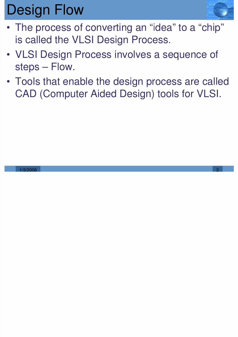
Design Flow
• The process of converting an “idea” to a “chip”is called the VLSI Design Process.
• VLSI Design Process involves a sequence ofsteps – Flow.
• Tools that enable the design process are called
CAD (Computer Aided Design) tools for VLSI.

8/14/2019 Cs623 – Cad for Vlsi Lecture 2
http://slidepdf.com/reader/full/cs623-cad-for-vlsi-lecture-2 3/19
31/3/2006
Abstraction Hierarchy
• Designers use different abstraction domains forVLSI design.
• Structural Domain
– Set of primitive components.
– Primitive components are interconnected to form
larger components.
• Behavioral Domain
– Components are defined by their input/outputresponse.
– The components can themselves be implemented
in many ways.

8/14/2019 Cs623 – Cad for Vlsi Lecture 2
http://slidepdf.com/reader/full/cs623-cad-for-vlsi-lecture-2 4/19
41/3/2006
Gajski’s Chart
8/14/2019 Cs623 – Cad for Vlsi Lecture 2
http://slidepdf.com/reader/full/cs623-cad-for-vlsi-lecture-2 5/19
51/3/2006
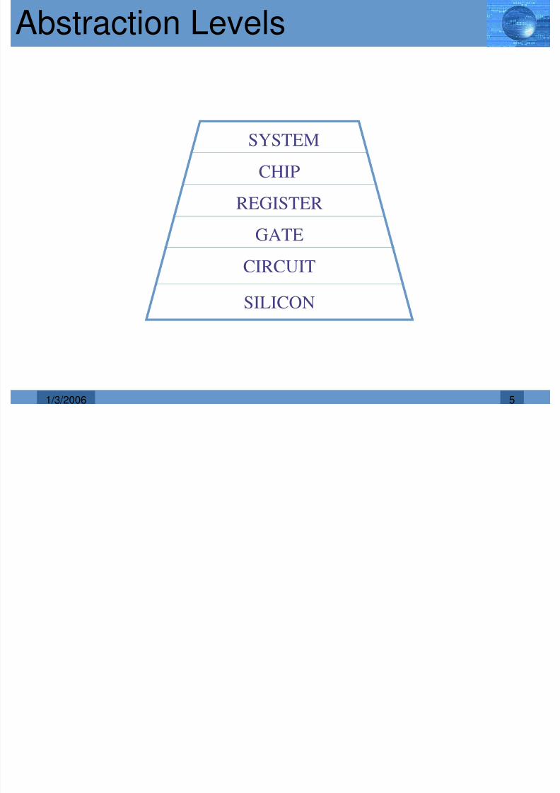
Abstraction Levels
SYSTEM
CHIP
REGISTER
GATE
CIRCUIT
SILICON

8/14/2019 Cs623 – Cad for Vlsi Lecture 2
http://slidepdf.com/reader/full/cs623-cad-for-vlsi-lecture-2 6/1961/3/2006
Silicon Level

8/14/2019 Cs623 – Cad for Vlsi Lecture 2
http://slidepdf.com/reader/full/cs623-cad-for-vlsi-lecture-2 7/1971/3/2006
Circuit Level
Inverter
N
D
P
SV+
G
Vin Vo
ut
D
G
S

8/14/2019 Cs623 – Cad for Vlsi Lecture 2
http://slidepdf.com/reader/full/cs623-cad-for-vlsi-lecture-2 8/1981/3/2006
Gate Level
SR Flip Flop
S
Q
Q
R
Q
QR
S

8/14/2019 Cs623 – Cad for Vlsi Lecture 2
http://slidepdf.com/reader/full/cs623-cad-for-vlsi-lecture-2 9/1991/3/2006
Register Level
REG
REG
INC
MUX
CLK B
CLK A
8/14/2019 Cs623 – Cad for Vlsi Lecture 2
http://slidepdf.com/reader/full/cs623-cad-for-vlsi-lecture-2 10/19101/3/2006
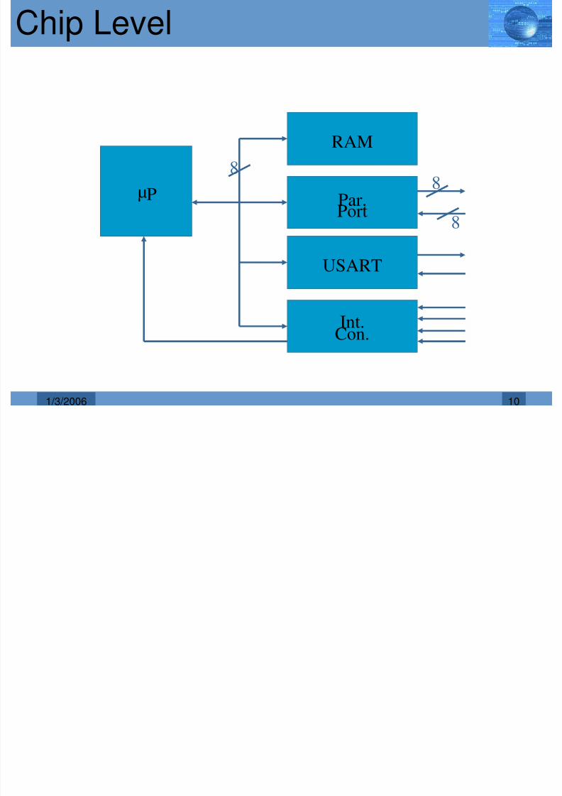
Chip Level
µ
88
8
RAM
Par.
Port
USART
Int.Con.
P

8/14/2019 Cs623 – Cad for Vlsi Lecture 2
http://slidepdf.com/reader/full/cs623-cad-for-vlsi-lecture-2 11/19111/3/2006
Typical Design Track
Behavioral Structural
English
Algorithmic
Data FlowLogic
Circuit
Geometrical
Layout
System
Chip
Register
Gate
Circuit
Layout
D i R i

8/14/2019 Cs623 – Cad for Vlsi Lecture 2
http://slidepdf.com/reader/full/cs623-cad-for-vlsi-lecture-2 12/19121/3/2006
Design Representation
• Done in many ways• Pictures
• Text• Is picture worth a thousand words?

8/14/2019 Cs623 – Cad for Vlsi Lecture 2
http://slidepdf.com/reader/full/cs623-cad-for-vlsi-lecture-2 13/19131/3/2006
Design Representation Using Pictures
R
TWO_CONZ
X
CLK
Block diagram
S0
S1 S2
R
1/00/0
1/0
0/0
0/1
State diagram
Specification: Detect inputs
that are identical and in
sequence
1/1
A Ti i Di
8/14/2019 Cs623 – Cad for Vlsi Lecture 2
http://slidepdf.com/reader/full/cs623-cad-for-vlsi-lecture-2 14/19141/3/2006
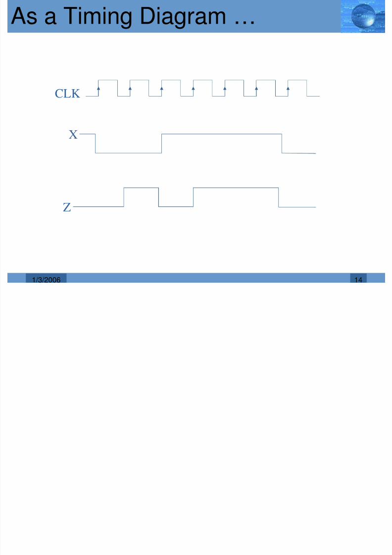
As a Timing Diagram …
CLK
X
Z
A St t T bl

8/14/2019 Cs623 – Cad for Vlsi Lecture 2
http://slidepdf.com/reader/full/cs623-cad-for-vlsi-lecture-2 15/19151/3/2006
As a State Table
S2/1S1/0S2
S2/0S1/1S1
S2/0S1/0S010
X
State
11S2
01S1
00S0y1y0
Code
State
STATE TABLE
STATE
ASSIGNMENT
A Ci it

8/14/2019 Cs623 – Cad for Vlsi Lecture 2
http://slidepdf.com/reader/full/cs623-cad-for-vlsi-lecture-2 16/19
161/3/2006
As a Circuit
D Q
QR
D Q
QR
X
CLK
R
I
Z
Y1
Y0
A d i V il

8/14/2019 Cs623 – Cad for Vlsi Lecture 2
http://slidepdf.com/reader/full/cs623-cad-for-vlsi-lecture-2 17/19
171/3/2006
And in Verilogmodule detector (Xin,clk,R,I,Zout);
input Xin,clk,R,I;output Zout;reg Y1,Y0;
initial begin
Y1 = 1'b0; Y0 = 1'b0;end
always @(posedge clk or negedge R) begin
if(R == 1'b0) beginY1 = 1'b0; Y0 = 1'b0;
end
else begin
Y1 = Xin; Y0 = I;end
end
assign Zout = Y0 & ((!Y1 & !Xin) | (Y1 & Xin));
endmodule
HDL

8/14/2019 Cs623 – Cad for Vlsi Lecture 2
http://slidepdf.com/reader/full/cs623-cad-for-vlsi-lecture-2 18/19
181/3/2006
HDL
• HDL stands for Hardware DescriptionLanguage
• Definition : A high level programming languageused to model hardware.
• Hardware Description Languages
– have special hardware related constructs.
– currently model digital systems, and in future can
model analog systems also. – can be used to build models for simulation,
synthesis and test.
– have been extended to the system design level.
Why Use HDLs?

8/14/2019 Cs623 – Cad for Vlsi Lecture 2
http://slidepdf.com/reader/full/cs623-cad-for-vlsi-lecture-2 19/19
191/3/2006
Why Use HDLs?• Allows textual representation of a design.
• High level language similar to C,C++.
• Can be used for Modeling at the
– Gate Level – Register Level
– Chip Level
• Can be used for many applications at the – Systems Level
– Circuit Level
– Switch Level• Design decomposition is simple with HDLs and hence
can manage complexity
• Early validation of designs.