csc 631: high-performance computer...
TRANSCRIPT

CSC 631: High-Performance Computer Architecture 1
CSC 631: High-Performance Computer Architecture
Spring 2017Lecture 9: Memory
Part I
CSC 631: High-Performance Computer Architecture 2
Introduction
• Programmers want unlimited amounts of memory with low latency
• Fast memory technology is more expensive per bit than slower memory
CSC 631: High-Performance Computer Architecture 3
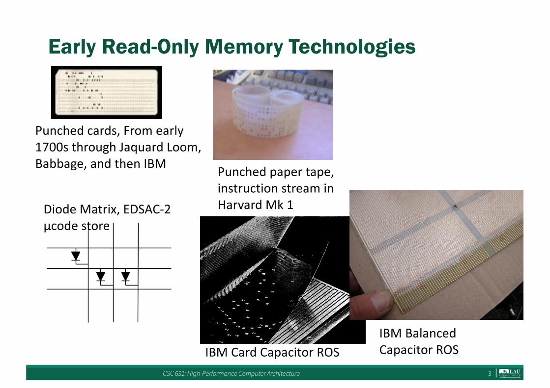
Early Read-Only Memory Technologies
Punchedcards,Fromearly1700sthroughJaquardLoom,Babbage,andthenIBM Punchedpapertape,
instructionstreaminHarvardMk1
IBMCardCapacitorROSIBMBalancedCapacitorROS
DiodeMatrix,EDSAC-2µcodestore

CSC 631: High-Performance Computer Architecture 4
Early Read/Write Main Memory Technologies
WilliamsTube,ManchesterMark1,1947
Babbage,1800s:Digitsstoredonmechanicalwheels
MercuryDelayLine,Univac1,1951
Also,regenerativecapacitormemoryonAtanasoff-Berrycomputer,androtatingmagneticdrummemoryonIBM650
CSC 631: High-Performance Computer Architecture 5
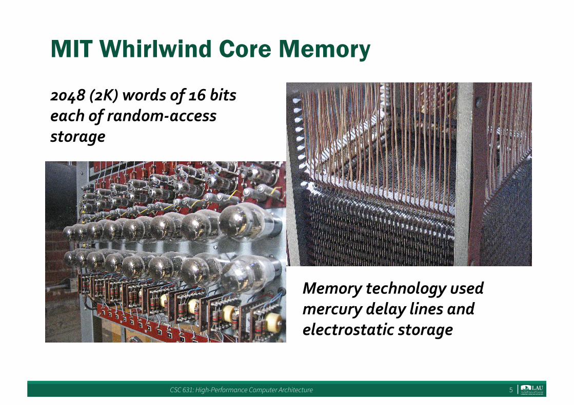
MIT Whirlwind Core Memory
2048 (2K) words of 16 bits each of random-access storage
Memory technology used mercury delay lines and electrostatic storage

CSC 631: High-Performance Computer Architecture 6
Core Memory• Core memory was first large scale reliable main memory
– invented by Forrester in late 40s/early 50s at MIT for Whirlwind project
• Bits stored as magnetization polarity on small ferrite cores threaded onto two-dimensional grid of wires
• Coincident current pulses on X and Y wires would write cell and also sense original state (destructive reads)
DECPDP-8/EBoard,4Kwordsx12bits,(1968)
§ Robust,non-volatilestorage§ Usedonspaceshuttlecomputers§ Coresthreadedontowiresbyhand
(25billionayearatpeakproduction)§ Coreaccesstime~1µs

CSC 631: High-Performance Computer Architecture 7
Semiconductor Memory
• Semiconductor memory began to be competitive in early 1970s– Intel formed to exploit market for semiconductor memory– Early semiconductor memory was Static RAM (SRAM).
• First commercial Dynamic RAM (DRAM) was Intel 1103– 1Kbit of storage on single chip– charge on a capacitor used to hold value– Value has to be regularly read and written back, hence
dynamic
• Semiconductor memory quickly replaced core in ‘70s
CSC 631: High-Performance Computer Architecture 8
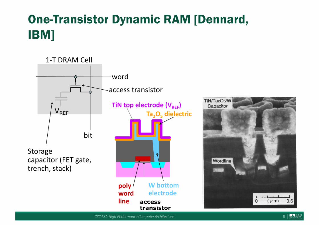
One-Transistor Dynamic RAM [Dennard, IBM]
TiNtopelectrode(VREF)Ta2O5 dielectric
Wbottomelectrode
polywordline access
transistor
1-TDRAMCell
word
bit
accesstransistor
Storagecapacitor(FETgate,trench,stack)
VREF
CSC 631: High-Performance Computer Architecture 9
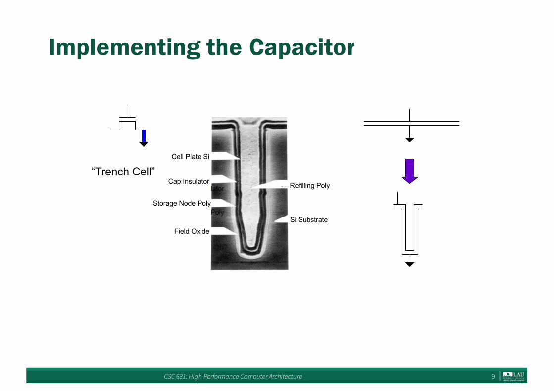
Implementing the Capacitor
“Trench Cell”Cell Plate Si
Cap Insulator
Storage Node Poly
Field Oxide
Refilling Poly
Si Substrate

CSC 631: High-Performance Computer Architecture 10
Modern DRAM Cell Structure
[Samsung,sub-70nmDRAM,2004]
CSC 631: High-Performance Computer Architecture 11
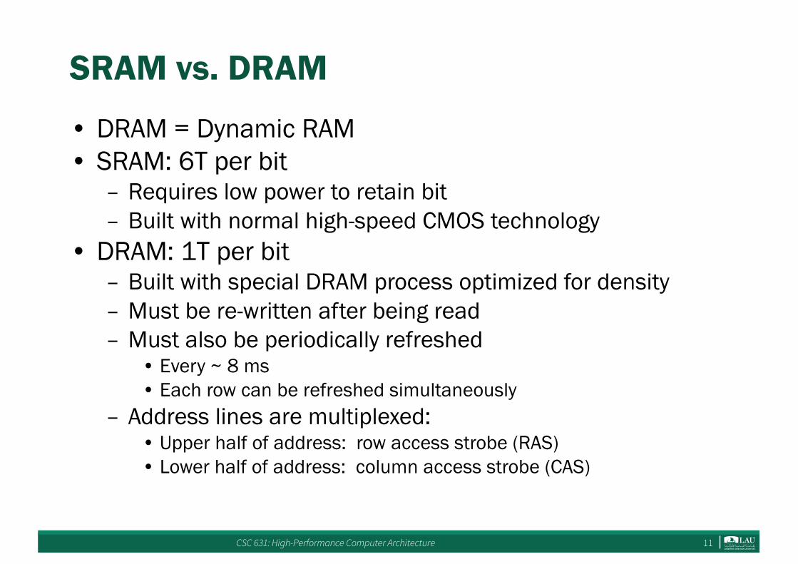
SRAM vs. DRAM
• DRAM = Dynamic RAM• SRAM: 6T per bit
– Requires low power to retain bit– Built with normal high-speed CMOS technology
• DRAM: 1T per bit– Built with special DRAM process optimized for density– Must be re-written after being read– Must also be periodically refreshed
• Every ~ 8 ms• Each row can be refreshed simultaneously
– Address lines are multiplexed:• Upper half of address: row access strobe (RAS)• Lower half of address: column access strobe (CAS)
CSC 631: High-Performance Computer Architecture 12
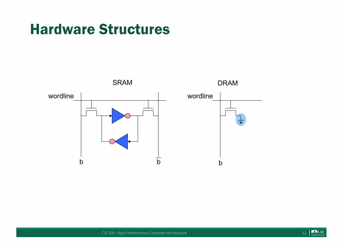
Hardware Structures
b b
SRAM
wordline
b
DRAM
wordline
CSC 631: High-Performance Computer Architecture 13
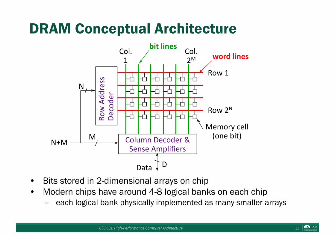
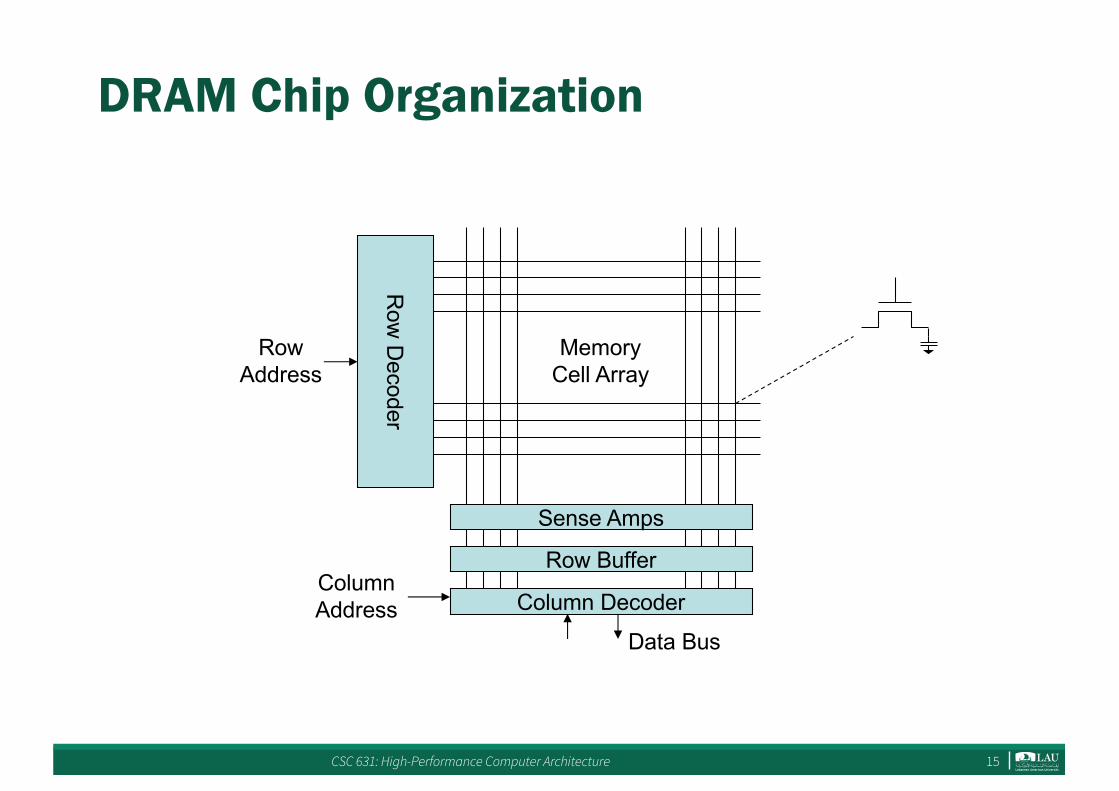
DRAM Conceptual Architecture
• Bits stored in 2-dimensional arrays on chip• Modern chips have around 4-8 logical banks on each chip
– each logical bank physically implemented as many smaller arrays
RowAdd
ress
Decode
r
Col.1
Col.2M
Row1
Row2N
ColumnDecoder&SenseAmplifiers
M
N
N+M
bitlineswordlines
Memorycell(onebit)
DData
CSC 631: High-Performance Computer Architecture 14
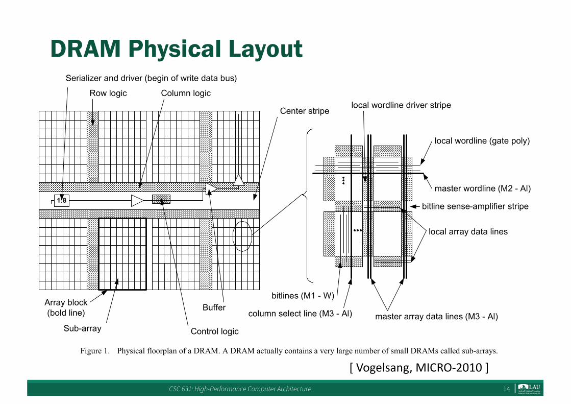
DRAM Physical Layout
II. DRAM TECHNOLOGY AND ARCHITECTURE
DRAMs are commoditized high volume products which need to have very low manufacturing costs. This puts significant constraints on the technology and architecture. The three most important factors for cost are the cost of a wafer, the yield and the die area. Cost of a wafer can be kept low if a simple transistor process and few metal levels are used. Yield can be optimized by process optimization and by optimizing the amount of redundancy. Die area optimization is achieved by keeping the array efficiency (ratio of cell area to total die area) as high as possible. The optimum approach changes very little even when the cell area is shrunk significantly over generations. DRAMs today use a transistor process with few junction optimizations, poly-Si gates and relatively high threshold voltage to suppress leakage. This process is much less expensive than a logic process but also much lower performance. It requires higher operating voltages than both high performance and low active power logic processes. Keeping array efficiency constant requires shrinking the area of the logic circuits on a DRAM at the same rate as the cell area. This is difficult as it is easier to shrink the very regular pattern of the cells than lithographically more complex circuitry. In addition the increasing complexity of the interface requires more circuit area.
Figure 1 shows the floorplan of a typical modern DDR2 or DDR3 DRAM and an enlargement of the cell array. The eight array blocks correspond to the eight banks of the DRAM. Row logic to decode the row address, implement row redundancy and drive the master wordlines is placed between the banks. At the other edge of the banks column
logic includes column address decoding, column redundancy and drivers for the column select lines as well as the secondary sense-amplifiers which sense or drive the array master data lines. The center stripe contains all other logic: the data and control pads and interface, central control logic, voltage regulators and pumps of the power system and circuitry to support efficient manufacturing test. Circuitry and buses in the center stripe are usually shared between banks to save area. Concurrent operation of banks is therefore limited to that portion of an operation that takes place inside a bank. For example the delay between two activate commands to different banks is limited by the time it takes to decode commands and addresses and trigger the command at a bank. Interleaving of reads and writes from and to different banks is limited by data contention on the shared data bus in the center stripe. Operations inside different banks can take place concurrently; one bank can for example be activating or precharging a wordline while another bank is simultaneously streaming data.
The enlargement of a small part of an array block at the right side of Figure 1 shows the hierarchical structure of the array block. Hierarchical wordlines and array data lines which were first developed in the early 1990s [5], [6] are now used by all major DRAM vendors. Master wordlines, column select lines and master array data lines are the interface between the array block and the rest of the DRAM circuitry. Individual cells connect to local wordlines and bitlines, bitlines are sensed or driven by bitline sense-amplifiers which connect to column select lines and local array data lines. The circuitry making the connection between local lines and master lines is placed in the local wordline driver stripe and bitline sense-amplifier stripe
Row logic Column logic
Serializer and driver (begin of write data bus)
Buffer
1:8
Control logicSub-array
Center stripe
column select line (M3 - Al) master array data lines (M3 - Al)
local array data lines
master wordline (M2 - Al)
local wordline (gate poly)
bitlines (M1 - W)
local wordline driver stripe
bitline sense-amplifier stripe
Array block (bold line)
Figure 1. Physical floorplan of a DRAM. A DRAM actually contains a very large number of small DRAMs called sub-arrays.
364
[Vogelsang,MICRO-2010]
CSC 631: High-Performance Computer Architecture 15
DRAM Chip Organization
Row
Decoder
Sense Amps
Column Decoder
MemoryCell Array
Row Buffer
RowAddress
ColumnAddress
Data Bus
CSC 631: High-Performance Computer Architecture 16
DRAM Chip Organization (2)
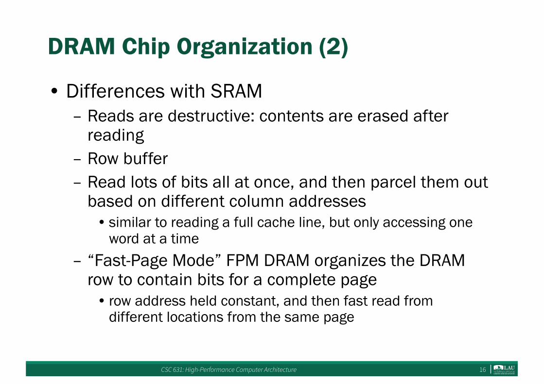
• Differences with SRAM– Reads are destructive: contents are erased after
reading– Row buffer– Read lots of bits all at once, and then parcel them out
based on different column addresses• similar to reading a full cache line, but only accessing one
word at a time– “Fast-Page Mode” FPM DRAM organizes the DRAM
row to contain bits for a complete page• row address held constant, and then fast read from
different locations from the same page
CSC 631: High-Performance Computer Architecture 17
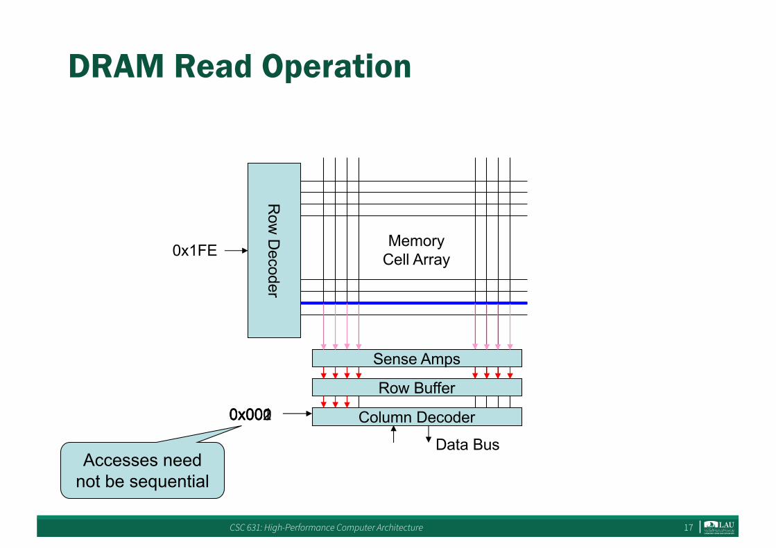
DRAM Read Operation
Row
Decoder
Sense Amps
Column Decoder
MemoryCell Array
Row Buffer
0x1FE
0x000
Data Bus
0x0010x002
Accesses need not be sequential
CSC 631: High-Performance Computer Architecture 18
Row Buffer
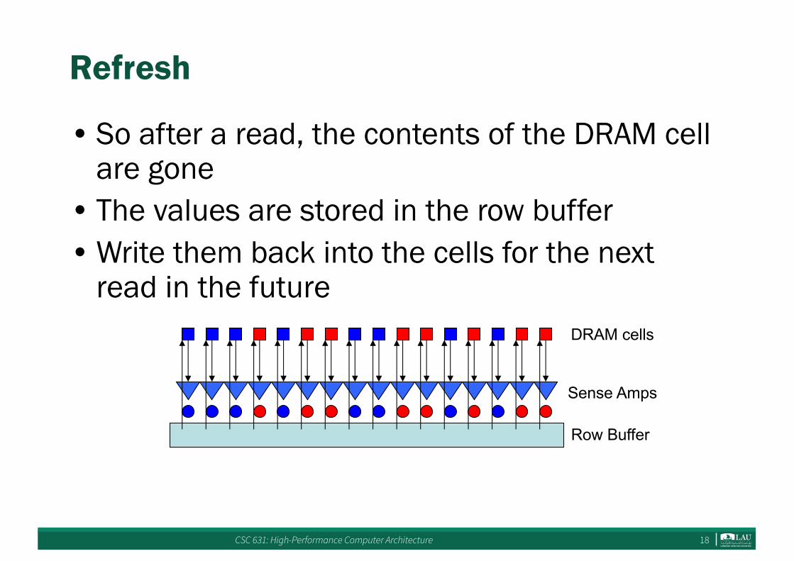
Refresh
• So after a read, the contents of the DRAM cell are gone
• The values are stored in the row buffer• Write them back into the cells for the next
read in the future
Sense Amps
DRAM cells
CSC 631: High-Performance Computer Architecture 19
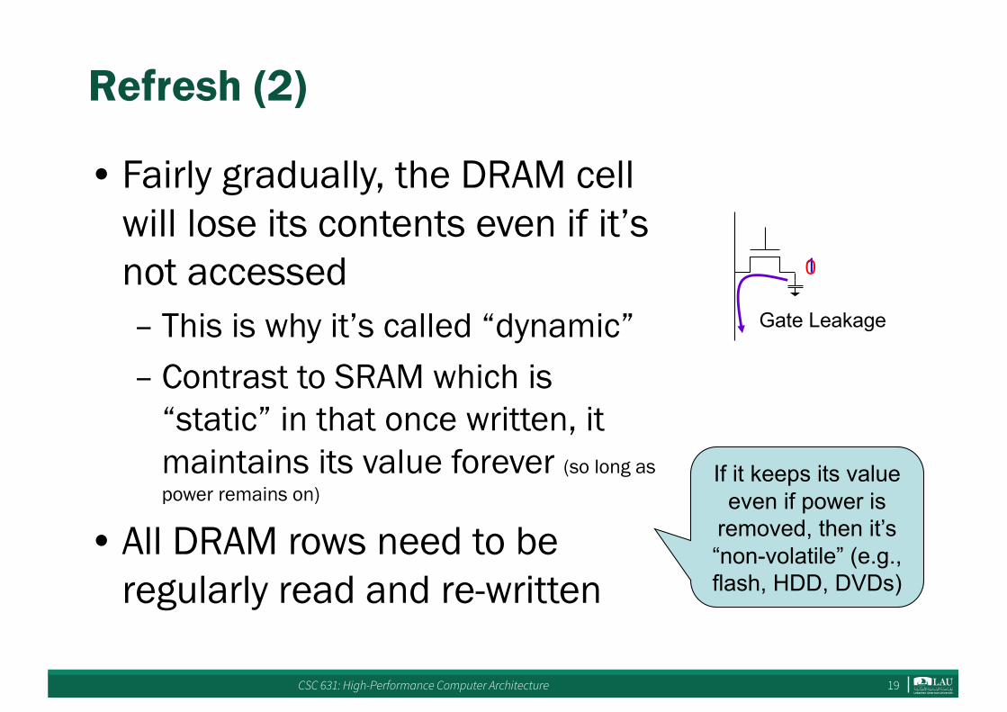
Refresh (2)
• Fairly gradually, the DRAM cell will lose its contents even if it’s not accessed– This is why it’s called “dynamic”– Contrast to SRAM which is
“static” in that once written, it maintains its value forever (so long as power remains on)
• All DRAM rows need to be regularly read and re-written
1
Gate Leakage
0
If it keeps its value even if power is
removed, then it’s “non-volatile” (e.g., flash, HDD, DVDs)

CSC 631: High-Performance Computer Architecture 20
MemoryController
Memory Controller
Scheduler Buffer
Bank 0 Bank 1
CommandsData
ReadQueue
WriteQueue
ResponseQueue
To/From CPU
Like Write-Combining Buffer,Scheduler may coalesce multipleaccesses together, or re-order toreduce number of row accesses
CSC 631: High-Performance Computer Architecture 21
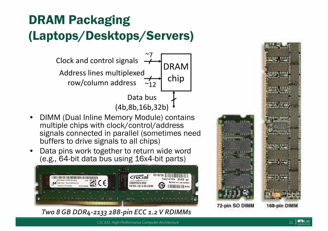
DRAM Packaging(Laptops/Desktops/Servers)
• DIMM (Dual Inline Memory Module) contains multiple chips with clock/control/address signals connected in parallel (sometimes need buffers to drive signals to all chips)
• Data pins work together to return wide word (e.g., 64-bit data bus using 16x4-bit parts)
Addresslinesmultiplexedrow/columnaddress
Clockandcontrolsignals
Databus(4b,8b,16b,32b)
DRAMchip
~12
~7
Two 8 GB DDR4-2133 288-pin ECC 1.2 V RDIMMs
CSC 631: High-Performance Computer Architecture 22
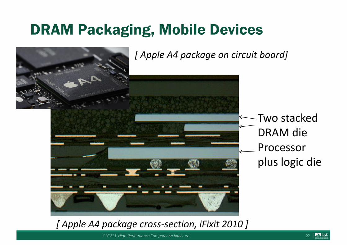
DRAM Packaging, Mobile Devices
[AppleA4packagecross-section,iFixit2010]
TwostackedDRAMdieProcessorpluslogicdie
[AppleA4packageoncircuitboard]
CSC 631: High-Performance Computer Architecture 23
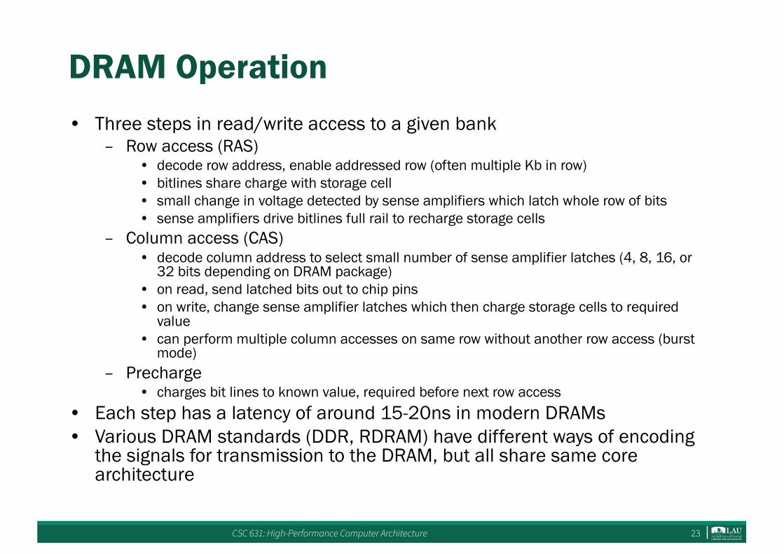
DRAM Operation• Three steps in read/write access to a given bank
– Row access (RAS)• decode row address, enable addressed row (often multiple Kb in row)• bitlines share charge with storage cell• small change in voltage detected by sense amplifiers which latch whole row of bits• sense amplifiers drive bitlines full rail to recharge storage cells
– Column access (CAS)• decode column address to select small number of sense amplifier latches (4, 8, 16, or
32 bits depending on DRAM package)• on read, send latched bits out to chip pins• on write, change sense amplifier latches which then charge storage cells to required
value• can perform multiple column accesses on same row without another row access (burst
mode)– Precharge
• charges bit lines to known value, required before next row access• Each step has a latency of around 15-20ns in modern DRAMs• Various DRAM standards (DDR, RDRAM) have different ways of encoding
the signals for transmission to the DRAM, but all share same core architecture

CSC 631: High-Performance Computer Architecture 24
Memory Parameters
• Latency– Time from initiation to completion of one memory read
(e.g., in nanoseconds, or in CPU or DRAM clock cycles)• Occupancy
– Time that a memory bank is busy with one request– Usually the important parameter for a memory write
• Bandwidth– Rate at which requests can be processed (accesses/sec,
or GB/s)
• All can vary significantly for reads vs. writes, or address, or address history (e.g., open/close page on DRAM bank)

CSC 631: High-Performance Computer Architecture 25
More Latency
Width/Speed variesdepending on memory type
Significant wire delay just getting fromthe CPU to the memory controller
More wire delay gettingto the memory chips
(plus the return trip…)

CSC 631: High-Performance Computer Architecture 26
Views of Memory
• Real machines have limited amounts of memory– 640KB? 4GB? 16 GB?
• Programmer doesn’t want to be bothered– Do you think, “oh, this computer only has 128MB
so I’ll write my code this way…”– What happens if you run on a different machine?
CSC 631: High-Performance Computer Architecture 27
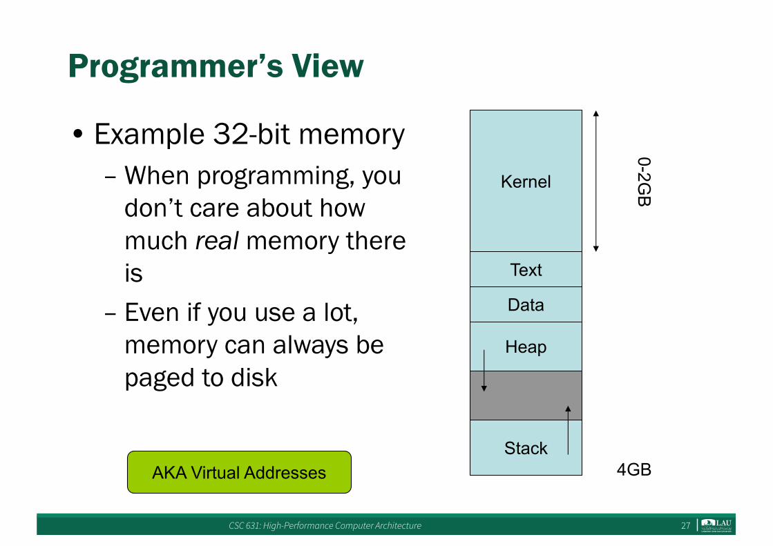
Programmer’s View
• Example 32-bit memory– When programming, you
don’t care about how much real memory there is
– Even if you use a lot, memory can always be paged to disk
Kernel
Text
Data
Heap
Stack
0-2GB
4GBAKA Virtual Addresses
CSC 631: High-Performance Computer Architecture 28
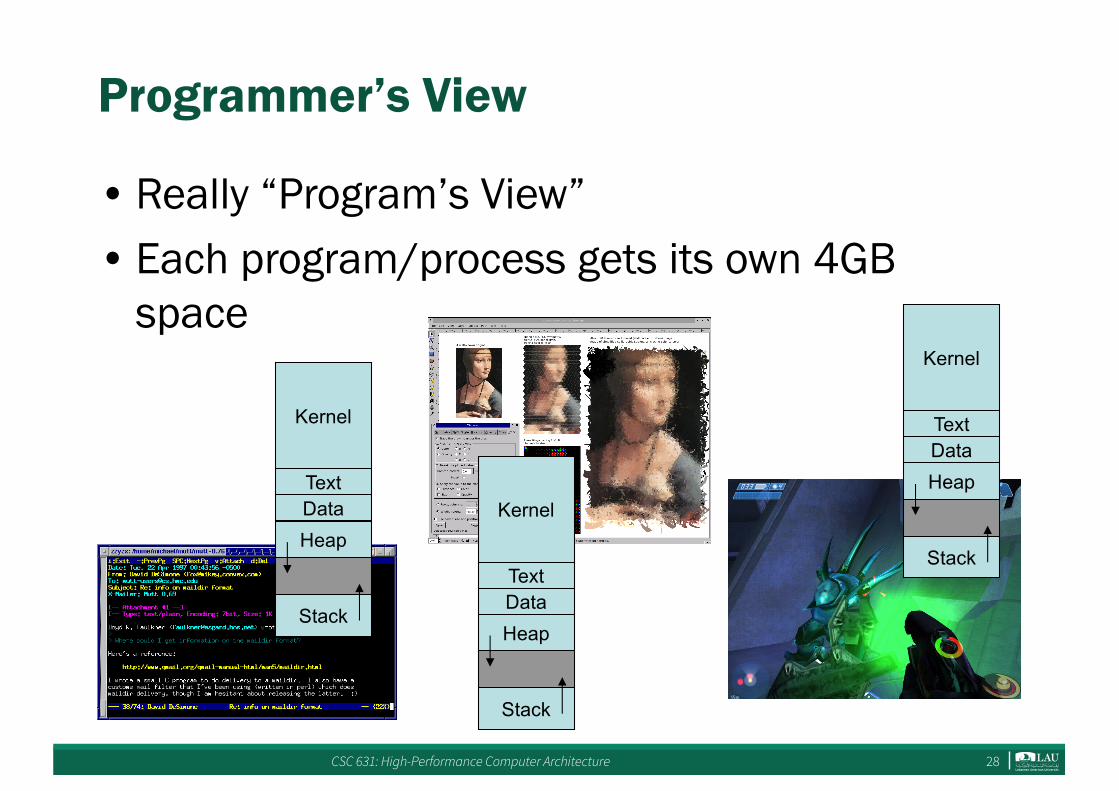
Programmer’s View
• Really “Program’s View”• Each program/process gets its own 4GB
space
Kernel
TextDataHeap
Stack
Kernel
TextDataHeap
Stack
Kernel
TextDataHeap
Stack

CSC 631: High-Performance Computer Architecture 29
CPU’s View
• At some point, the CPU is going to have to load-from/store-to memory… all it knows is the real, A.K.A. physical memory
• … which these daysbetween 4-32 GB

CSC 631: High-Performance Computer Architecture 30
Memory Technology
• Amdahl:– Memory capacity should grow linearly with processor
speed– Unfortunately, memory capacity and speed has not
kept pace with processors• Some optimizations:
– Multiple accesses to same row– Synchronous DRAM
• Added clock to DRAM interface• Burst mode with critical word first
– Wider interfaces– Double data rate (DDR)– Multiple banks on each DRAM device
CSC 631: High-Performance Computer Architecture 31
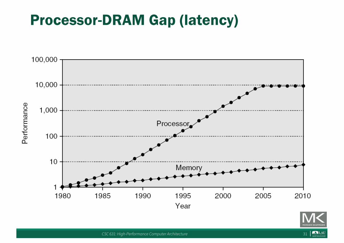
Processor-DRAM Gap (latency)

CSC 631: High-Performance Computer Architecture 32
Processor-DRAM Gap (latency)
Year
µProc60%/year
DRAM7%/year
1
10
100
100019
8019
81
1983
1984
1985
1986
1987
1988
1989
1990
1991
1992
1993
1994
1995
1996
1997
1998
1999
2000
DRAM
CPU
1982
Processor-MemoryPerformanceGap:(growing50%/yr)
Perfo
rmance
Four-issue3GHzsuperscalaraccessing100nsDRAMcouldexecute1,200instructionsduringtimeforonememoryaccess!
CSC 631: High-Performance Computer Architecture 33
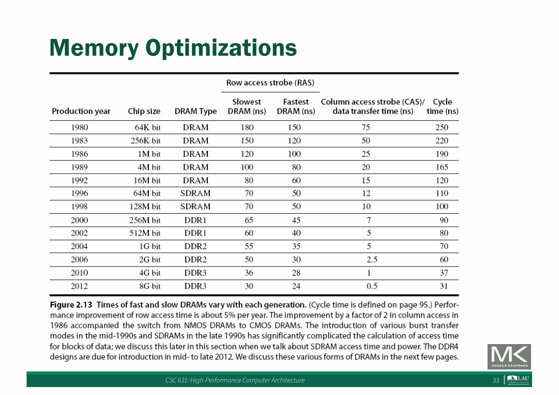
Memory Optimizations
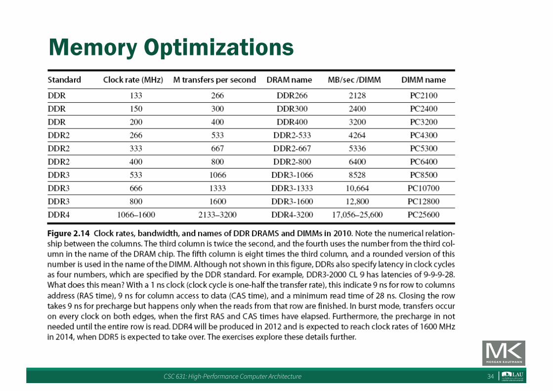
CSC 631: High-Performance Computer Architecture 34
Memory Optimizations
CSC 631: High-Performance Computer Architecture 35
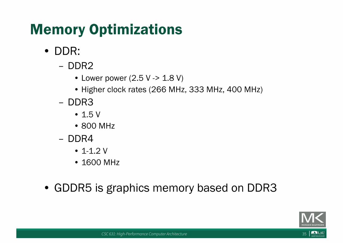
Memory Optimizations• DDR:
– DDR2• Lower power (2.5 V -> 1.8 V)• Higher clock rates (266 MHz, 333 MHz, 400 MHz)
– DDR3• 1.5 V• 800 MHz
– DDR4• 1-1.2 V• 1600 MHz
• GDDR5 is graphics memory based on DDR3

CSC 631: High-Performance Computer Architecture 36
Memory Optimizations
• Graphics memory:– Achieve 2-5 X bandwidth per DRAM vs. DDR3
•Wider interfaces (32 vs. 16 bit)•Higher clock rate
– Possible because they are attached via soldering instead of socketted DIMM modules
• Reducing power in SDRAMs:– Lower voltage– Low power mode (ignores clock, continues to
refresh)

CSC 631: High-Performance Computer Architecture 37
Memory Power Consumption

CSC 631: High-Performance Computer Architecture 38
Physical Size Affects Latency
SmallMemory
CPU
BigMemory
CPU
§ Signalshavefurthertotravel§ Fanouttomorelocations
CSC 631: High-Performance Computer Architecture 39
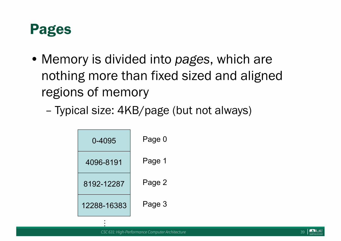
Pages
• Memory is divided into pages, which are nothing more than fixed sized and aligned regions of memory– Typical size: 4KB/page (but not always)
0-4095
4096-8191
8192-12287
12288-16383
…
Page 0
Page 1
Page 2
Page 3

CSC 631: High-Performance Computer Architecture 40
Page Table
• Map from virtual addresses to physical locations
0K4K8K12K
VirtualAddresses
0K4K8K12K16K20K24K28K
PhysicalAddresses
“Physical Location” mayinclude hard-disk
Page Table implementsthis VàP mapping

CSC 631: High-Performance Computer Architecture 41
Page Tables
0K4K8K12K
0K4K8K12K16K20K24K28K
0K4K8K12K
Physical Memory
CSC 631: High-Performance Computer Architecture 42
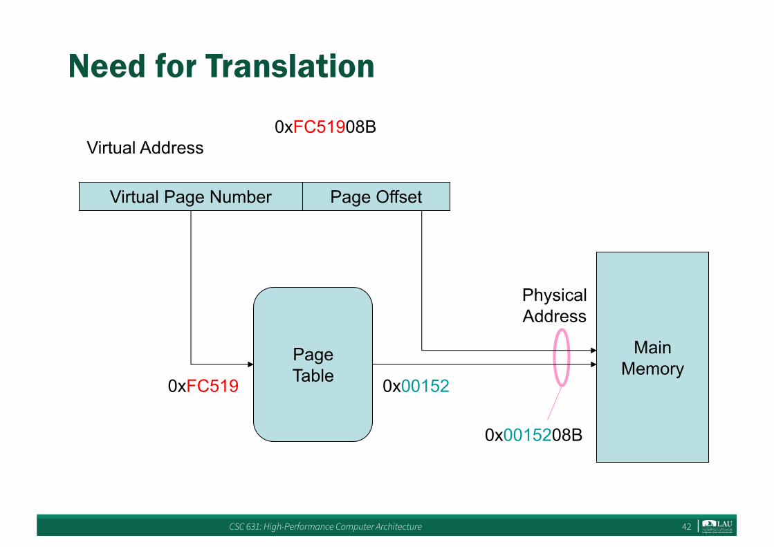
Need for Translation
Virtual Address
Virtual Page Number Page Offset
PageTable
MainMemory
PhysicalAddress
0xFC51908B
0x001520xFC519
0x0015208B
CSC 631: High-Performance Computer Architecture 43
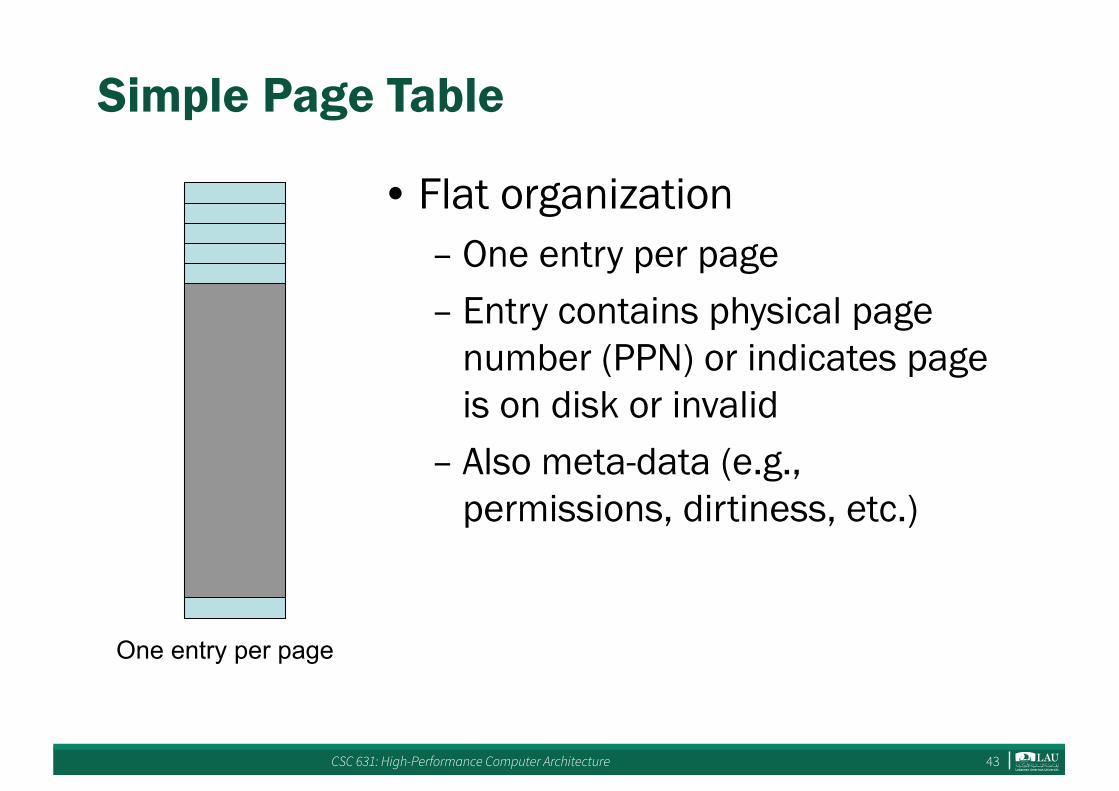
Simple Page Table
• Flat organization– One entry per page– Entry contains physical page
number (PPN) or indicates page is on disk or invalid
– Also meta-data (e.g., permissions, dirtiness, etc.)
One entry per page
CSC 631: High-Performance Computer Architecture 44
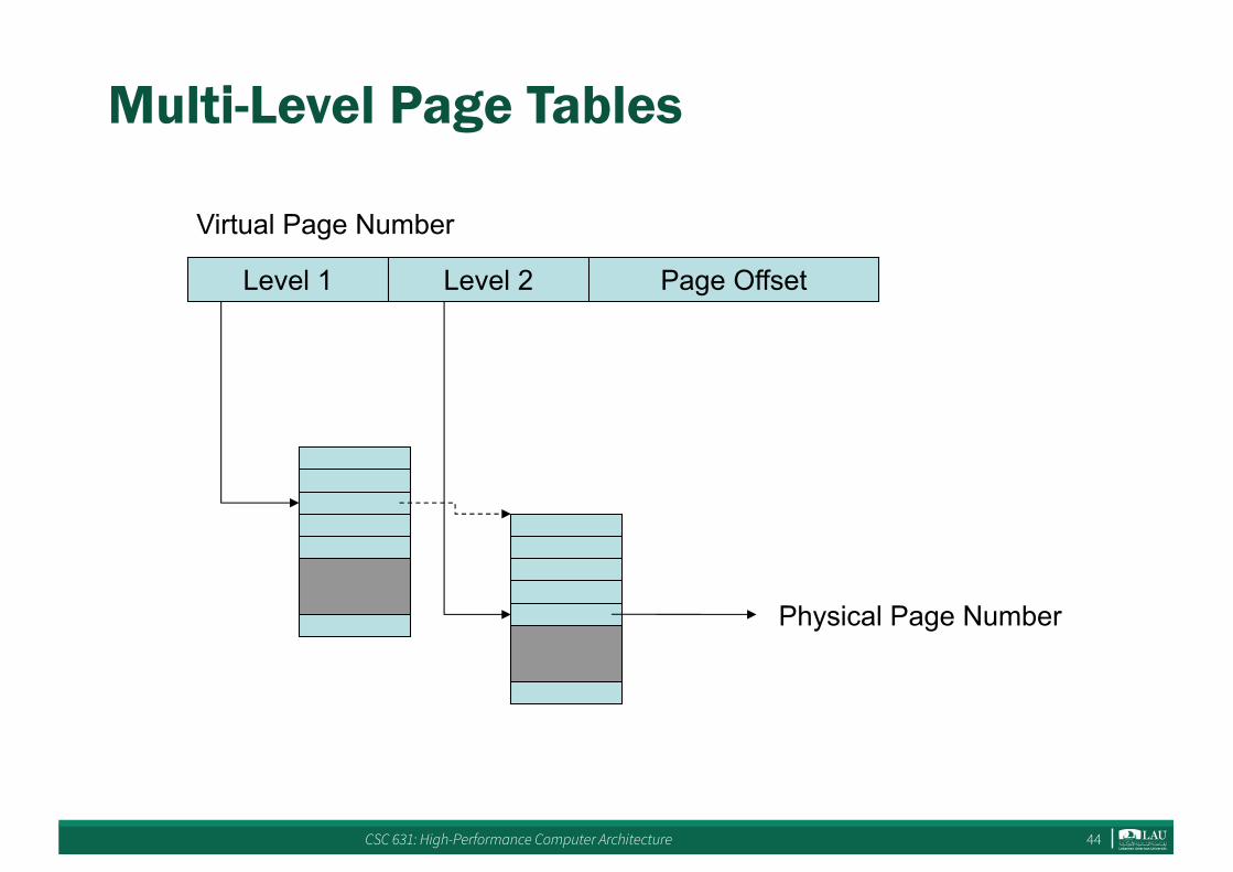
Multi-Level Page Tables
Level 1 Level 2 Page Offset
Physical Page Number
Virtual Page Number
CSC 631: High-Performance Computer Architecture 45
Choosing a Page Size
• Page size inversely proportional to page table overhead
• Large page size permits more efficient transfer to/from disk– vs. many small transfers– Like downloading from Internet
• Small page leads to less fragmentation– Big page likely to have more bytes unused

CSC 631: High-Performance Computer Architecture 46
• Program deals with virtual addresses– “Load R1 = 0[R2]”
• On memory instruction1. Compute virtual address (0[R2])2. Compute virtual page number3. Compute physical address of VPN’s page table
entry4. Load* mapping 5. Compute physical address6. Do the actual Load* from memory
CPU Memory Access
Could be more dependingOn page table organization

CSC 631: High-Performance Computer Architecture 47
Impact on Performance?
• Every time you load/store, the CPU must perform two (or more) accesses!
• Even worse, every fetch requires translation of the PC!
• Observation:– Once a virtual page is mapped into a physical
page, it’ll likely stay put for quite some time
CSC 631: High-Performance Computer Architecture 48
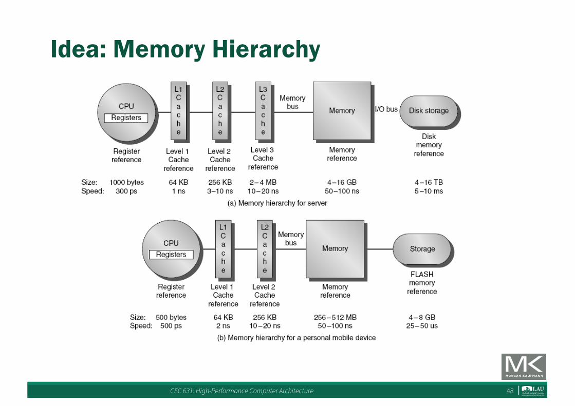
Idea: Memory Hierarchy
CSC 631: High-Performance Computer Architecture 49
Idea: Caching!
• Organize memory system into a hierarchy– Entire addressable memory space available in
largest, slowest memory– Incrementally smaller and faster memories, each
containing a subset of the memory below it, proceed in steps up toward the processor
• Temporal and spatial locality insures that nearly all references can be found in smaller memories– Gives the allusion of a large, fast memory being
presented to the processor

CSC 631: High-Performance Computer Architecture 50
Idea: Caching!
• Not caching of data, but caching of translations
0K4K8K12K
VirtualAddresses
0K4K8K12K16K20K24K28K
PhysicalAddresses
8 16
0 204 412 X
VPN 8
PPN 16
CSC 631: High-Performance Computer Architecture 51
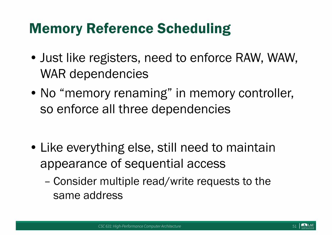
Memory Reference Scheduling
• Just like registers, need to enforce RAW, WAW, WAR dependencies
• No “memory renaming” in memory controller, so enforce all three dependencies
• Like everything else, still need to maintain appearance of sequential access– Consider multiple read/write requests to the
same address
CSC 631: High-Performance Computer Architecture 52
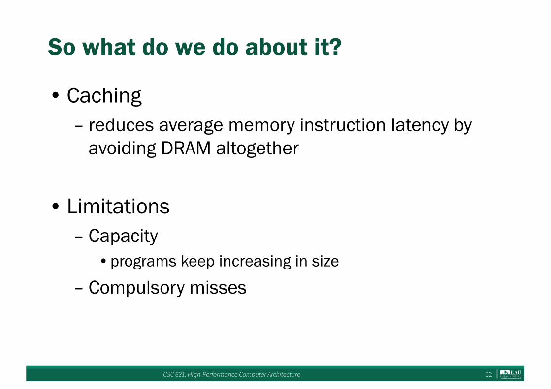
So what do we do about it?
• Caching– reduces average memory instruction latency by
avoiding DRAM altogether
• Limitations– Capacity
•programs keep increasing in size
– Compulsory misses
CSC 631: High-Performance Computer Architecture 53
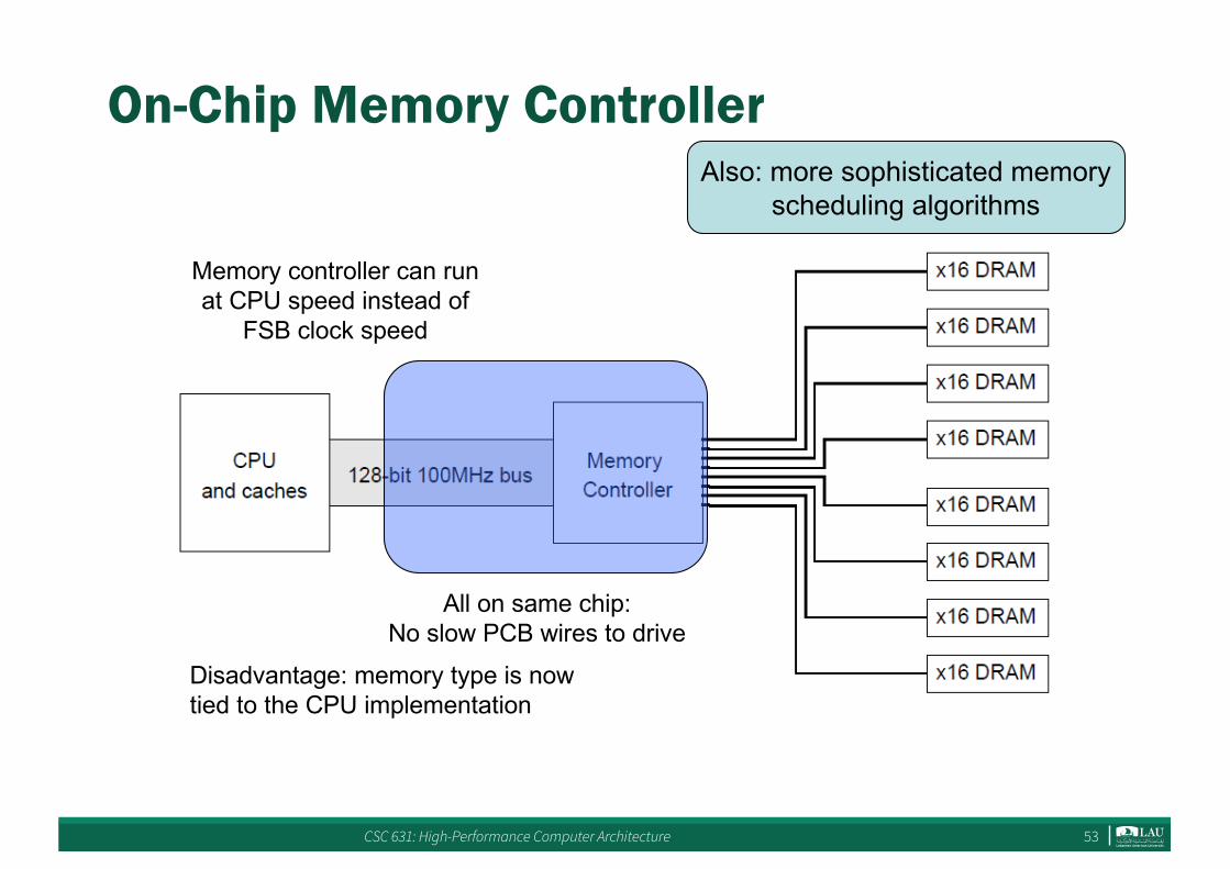
On-Chip Memory Controller
All on same chip:No slow PCB wires to drive
Memory controller can runat CPU speed instead of
FSB clock speed
Disadvantage: memory type is nowtied to the CPU implementation
Also: more sophisticated memoryscheduling algorithms
CSC 631: High-Performance Computer Architecture 54
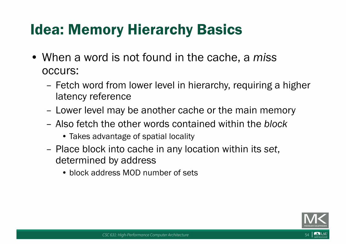
Idea: Memory Hierarchy Basics
• When a word is not found in the cache, a miss occurs:– Fetch word from lower level in hierarchy, requiring a higher
latency reference– Lower level may be another cache or the main memory– Also fetch the other words contained within the block
• Takes advantage of spatial locality– Place block into cache in any location within its set,
determined by address• block address MOD number of sets

CSC 631: High-Performance Computer Architecture 55
Memory Hierarchy Basics
• Cache memory– The level of the memory hierarchy closest to the CPU
• Given accesses X1, …, Xn–1, Xn
n How do we know if the data is present?
n Where do we look?

CSC 631: High-Performance Computer Architecture 56
Memory Hierarchy Basics
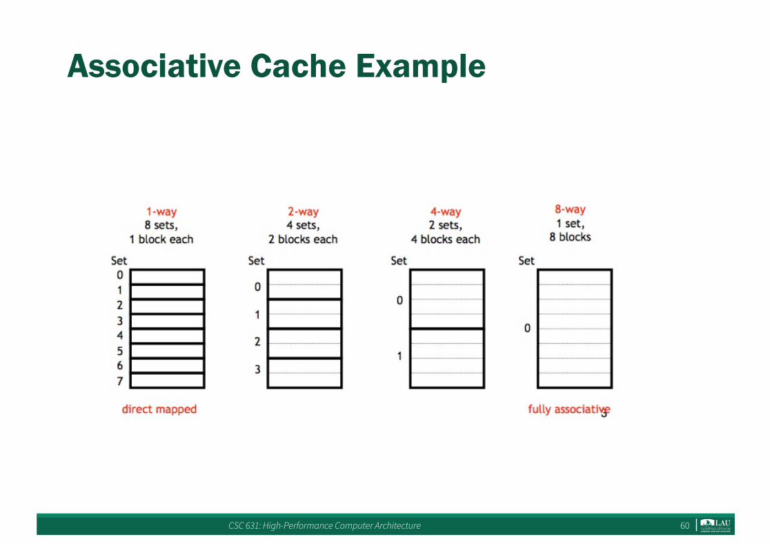
• n sets => n-way set associative– Direct-mapped cache => one block per set– Fully associative => one set
CSC 631: High-Performance Computer Architecture 57
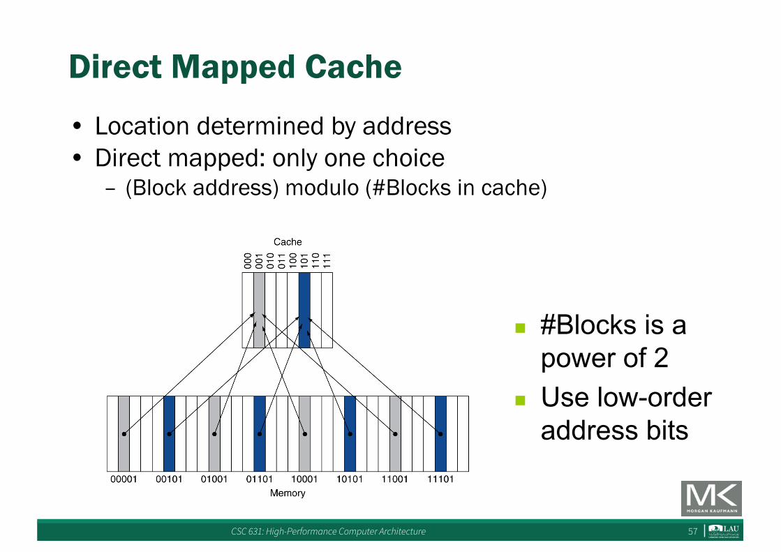
Direct Mapped Cache
• Location determined by address• Direct mapped: only one choice
– (Block address) modulo (#Blocks in cache)
n #Blocks is a power of 2
n Use low-order address bits

CSC 631: High-Performance Computer Architecture 58
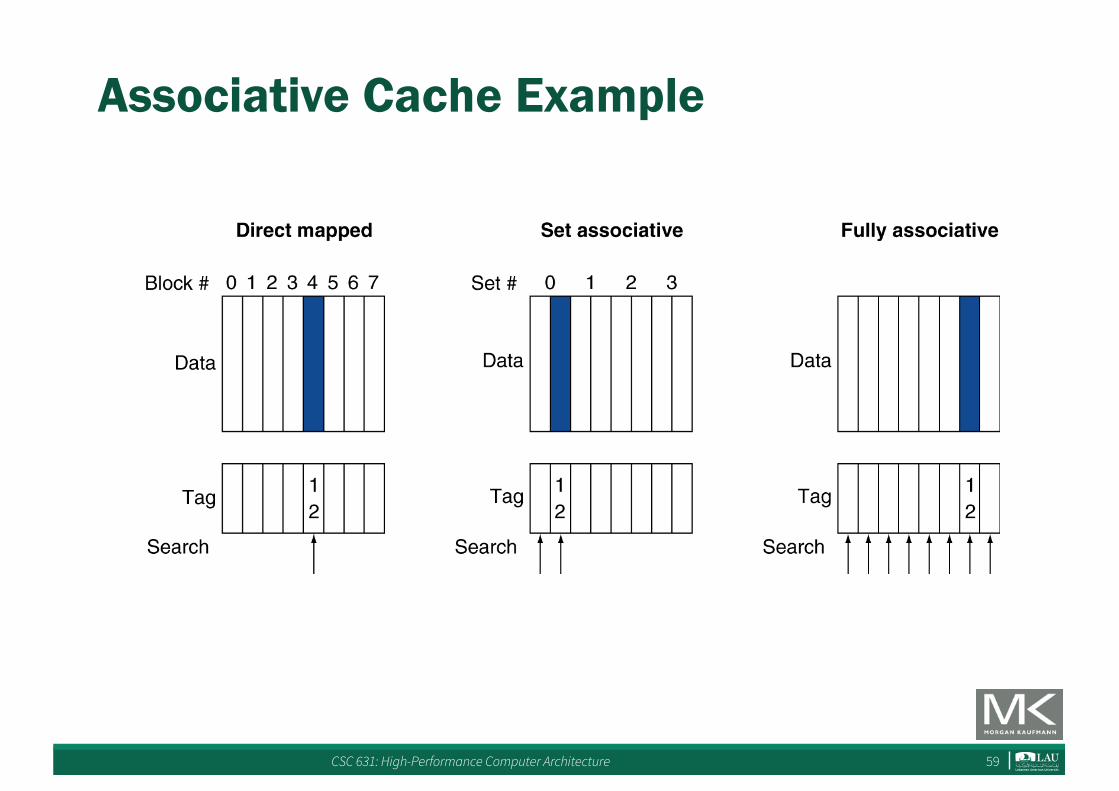
Associative Caches
• Fully associative– Allow a given block to go in any cache entry– Requires all entries to be searched at once– Comparator per entry (expensive)
• n-way set associative– Each set contains n entries– Block number determines which set
•(Block number) modulo (#Sets in cache)– Search all entries in a given set at once– n comparators (less expensive)
CSC 631: High-Performance Computer Architecture 59
Associative Cache Example
CSC 631: High-Performance Computer Architecture 60
Associative Cache Example
CSC 631: High-Performance Computer Architecture 61
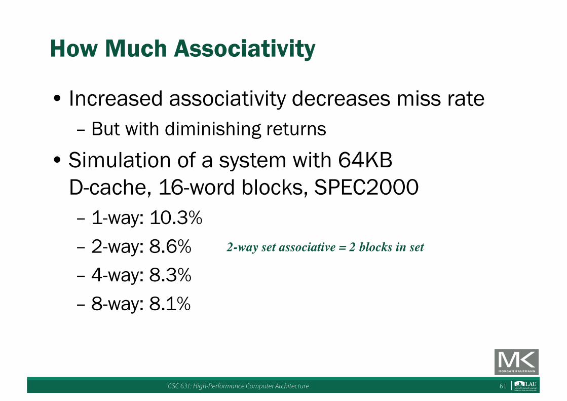
How Much Associativity
• Increased associativity decreases miss rate– But with diminishing returns
• Simulation of a system with 64KBD-cache, 16-word blocks, SPEC2000– 1-way: 10.3%– 2-way: 8.6%– 4-way: 8.3%– 8-way: 8.1%
2-way set associative = 2 blocks in set

CSC 631: High-Performance Computer Architecture 62
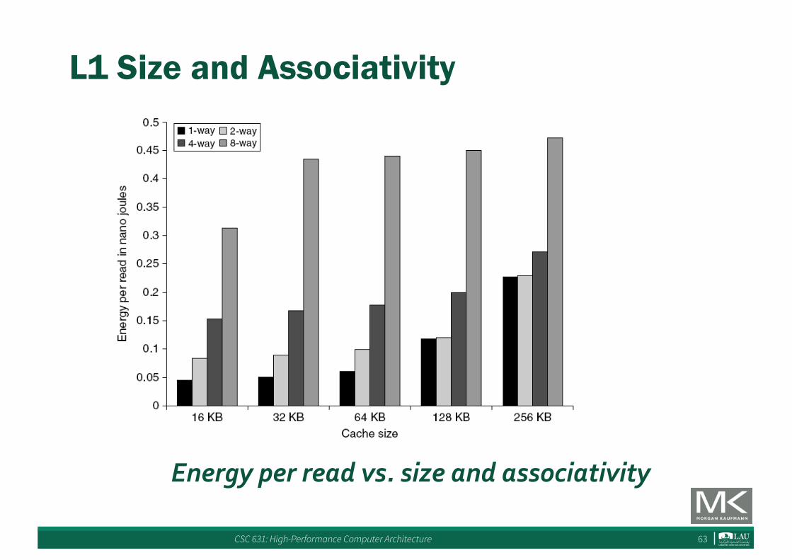
L1 Size and Associativity
Access time vs. size and associativity
CSC 631: High-Performance Computer Architecture 63
L1 Size and Associativity
Energy per read vs. size and associativity
CSC 631: High-Performance Computer Architecture 64
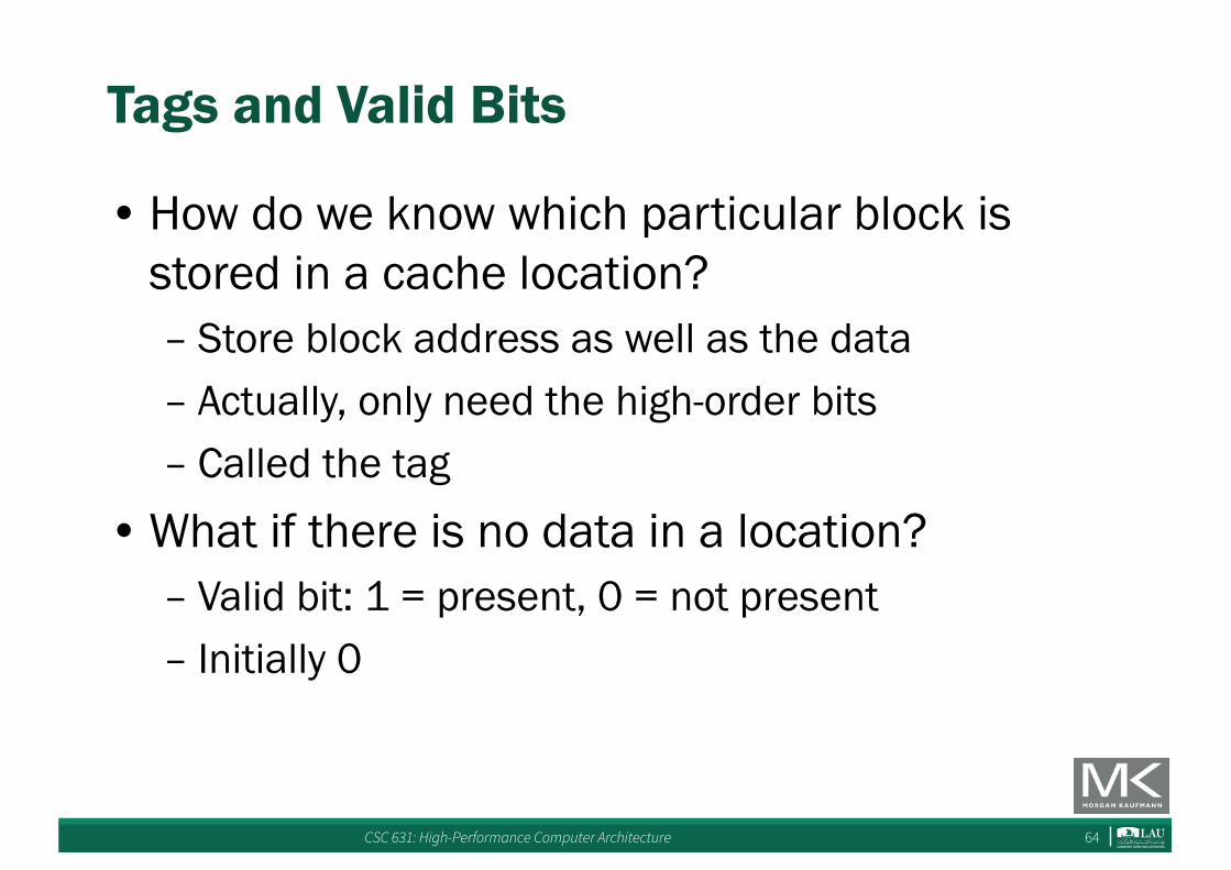
Tags and Valid Bits
• How do we know which particular block is stored in a cache location?– Store block address as well as the data– Actually, only need the high-order bits– Called the tag
• What if there is no data in a location?– Valid bit: 1 = present, 0 = not present– Initially 0

CSC 631: High-Performance Computer Architecture 65
Cache Example• 8-blocks, 1 word/block, direct mapped• Initial state
Index V Tag Data000 N001 N010 N011 N100 N101 N110 N111 N

CSC 631: High-Performance Computer Architecture 66
Cache Example
Index V Tag Data000 N001 N010 N011 N100 N101 N110 Y 10 Mem[10110]111 N
Word addr Binary addr Hit/miss Cache block22 10 110 Miss 110

CSC 631: High-Performance Computer Architecture 67
Cache Example
Index V Tag Data000 N001 N010 Y 11 Mem[11010]011 N100 N101 N110 Y 10 Mem[10110]111 N
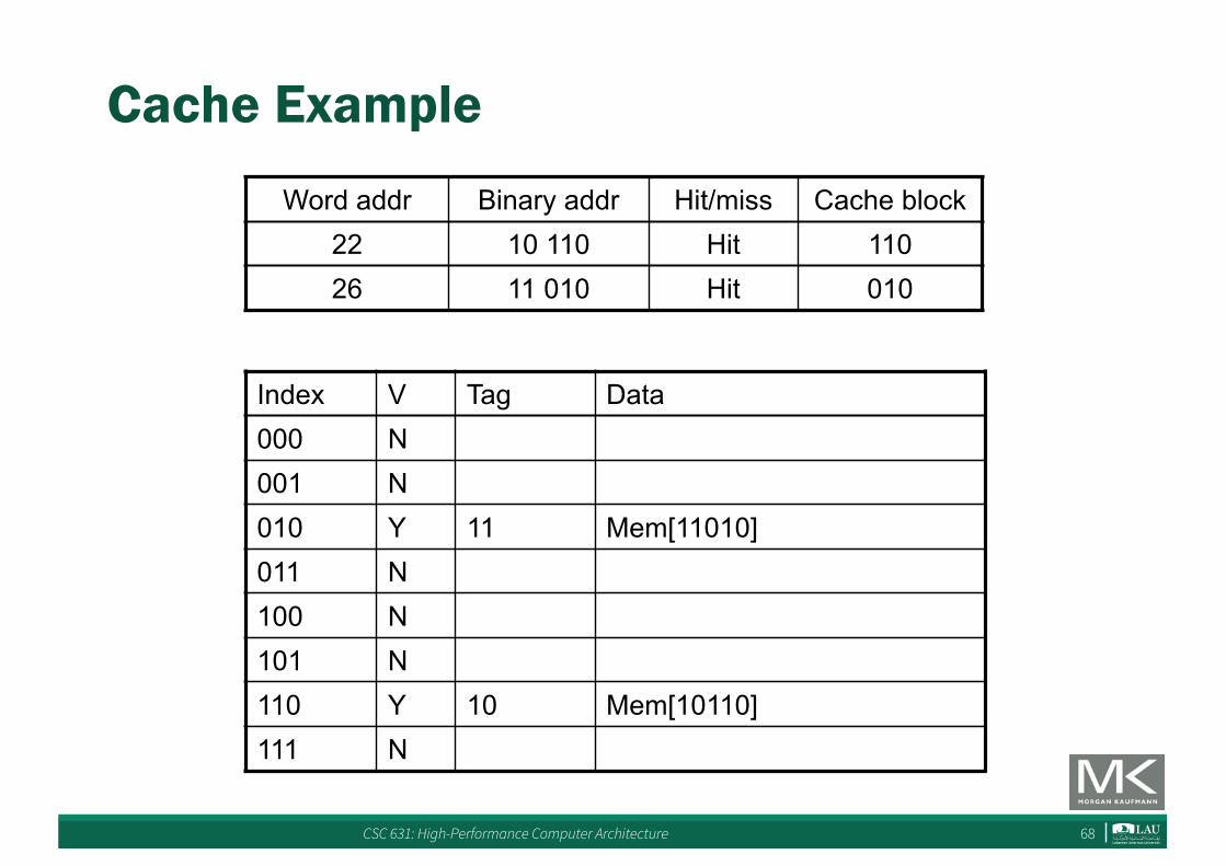
Word addr Binary addr Hit/miss Cache block26 11 010 Miss 010
CSC 631: High-Performance Computer Architecture 68
Cache Example
Index V Tag Data000 N001 N010 Y 11 Mem[11010]011 N100 N101 N110 Y 10 Mem[10110]111 N
Word addr Binary addr Hit/miss Cache block22 10 110 Hit 11026 11 010 Hit 010

CSC 631: High-Performance Computer Architecture 69
Cache Example
Index V Tag Data000 Y 10 Mem[10000]001 N010 Y 11 Mem[11010]011 Y 00 Mem[00011]100 N101 N110 Y 10 Mem[10110]111 N
Word addr Binary addr Hit/miss Cache block16 10 000 Miss 0003 00 011 Miss 01116 10 000 Hit 000
CSC 631: High-Performance Computer Architecture 70
Cache Example
Index V Tag Data000 Y 10 Mem[10000]001 N010 Y 10 Mem[10010]011 Y 00 Mem[00011]100 N101 N110 Y 10 Mem[10110]111 N
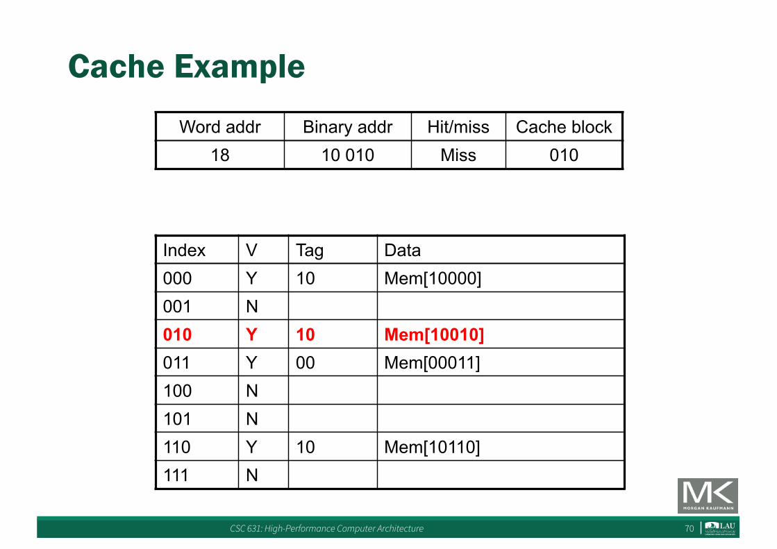
Word addr Binary addr Hit/miss Cache block18 10 010 Miss 010

CSC 631: High-Performance Computer Architecture 71
Address Subdivision
CSC 631: High-Performance Computer Architecture 72
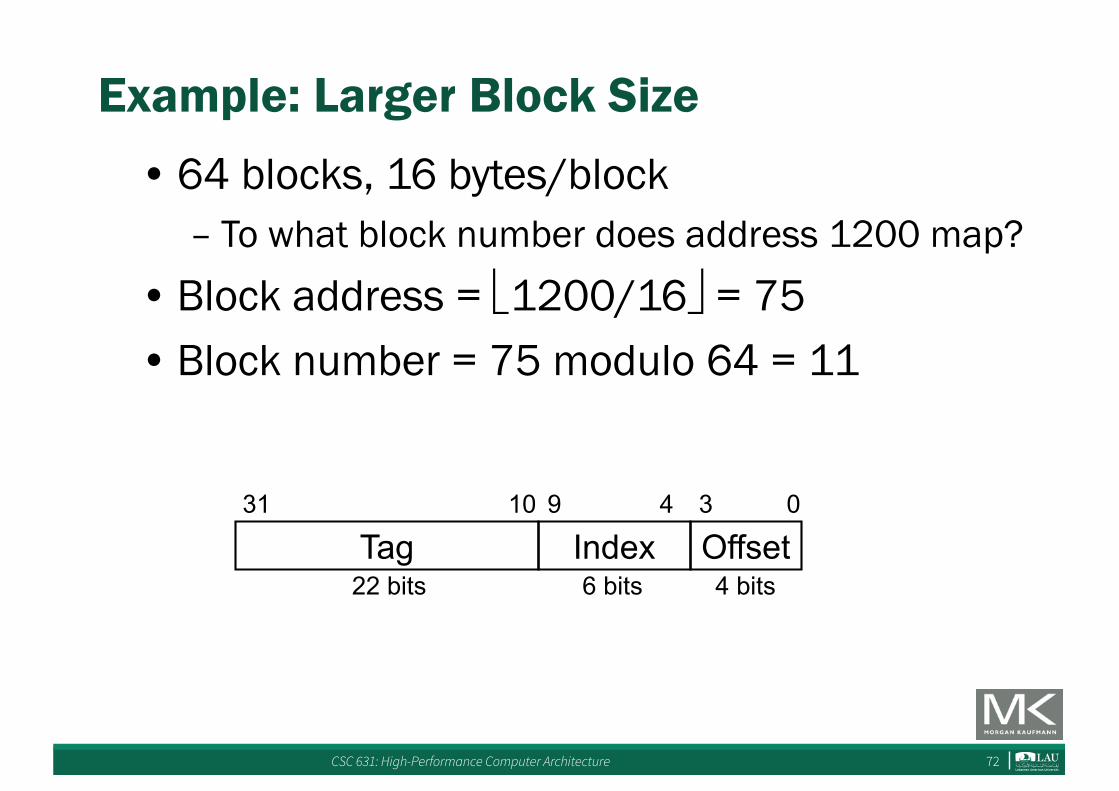
Example: Larger Block Size• 64 blocks, 16 bytes/block
– To what block number does address 1200 map?
• Block address = ë1200/16û = 75• Block number = 75 modulo 64 = 11
Tag Index Offset03491031
4 bits6 bits22 bits
CSC 631: High-Performance Computer Architecture 73
Block Size Considerations
• Larger blocks should reduce miss rate– Due to spatial locality
• But in a fixed-sized cache– Larger blocks Þ fewer of them
•More competition Þ increased miss rate
– Larger blocks Þ pollution
• Larger miss penalty– Can override benefit of reduced miss rate– Early restart and critical-word-first can help
CSC 631: High-Performance Computer Architecture 74
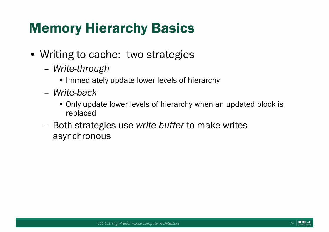
Memory Hierarchy Basics
• Writing to cache: two strategies– Write-through
• Immediately update lower levels of hierarchy– Write-back
• Only update lower levels of hierarchy when an updated block is replaced
– Both strategies use write buffer to make writes asynchronous
CSC 631: High-Performance Computer Architecture 75
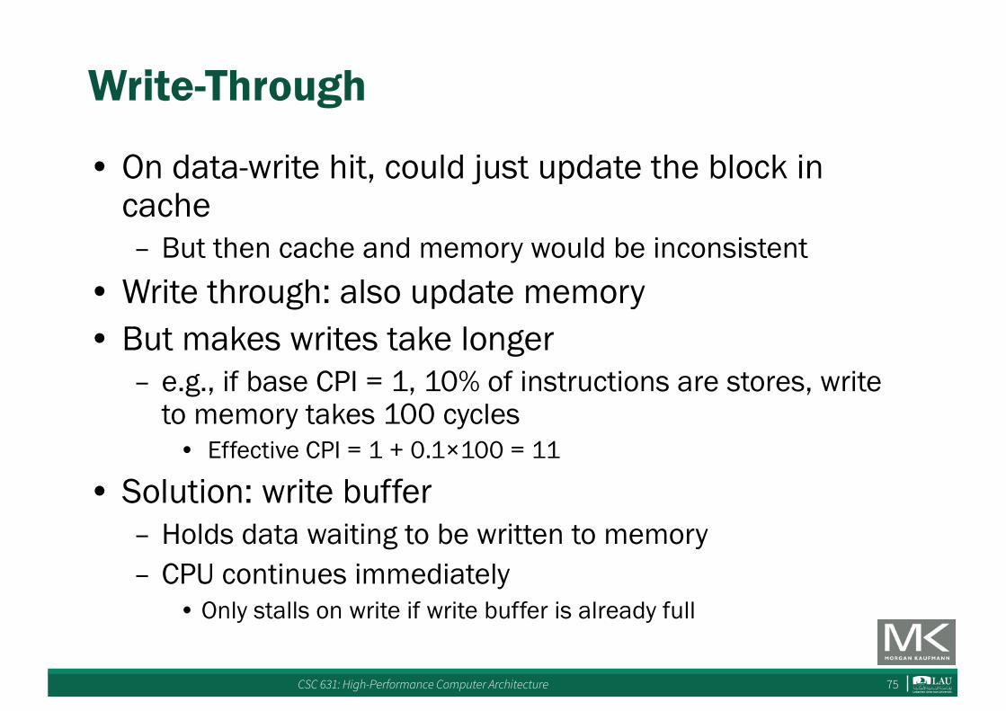
Write-Through
• On data-write hit, could just update the block in cache– But then cache and memory would be inconsistent
• Write through: also update memory• But makes writes take longer
– e.g., if base CPI = 1, 10% of instructions are stores, write to memory takes 100 cycles
• Effective CPI = 1 + 0.1×100 = 11
• Solution: write buffer– Holds data waiting to be written to memory– CPU continues immediately
• Only stalls on write if write buffer is already full
CSC 631: High-Performance Computer Architecture 76
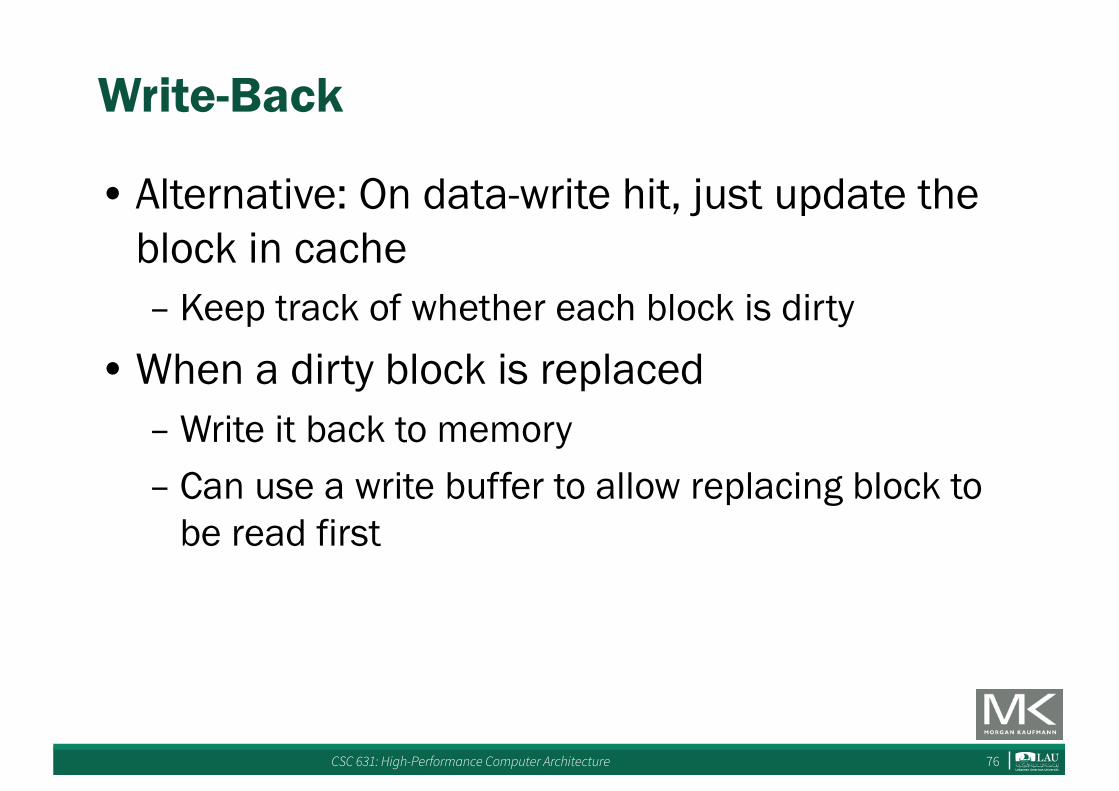
Write-Back
• Alternative: On data-write hit, just update the block in cache– Keep track of whether each block is dirty
• When a dirty block is replaced– Write it back to memory– Can use a write buffer to allow replacing block to
be read first

CSC 631: High-Performance Computer Architecture 77
Write Allocation
• What should happen on a write miss?• Alternatives for write-through
– Allocate on miss: fetch the block– Write around: don’t fetch the block
•Since programs often write a whole block before reading it (e.g., initialization)
• For write-back– Usually fetch the block
CSC 631: High-Performance Computer Architecture 78
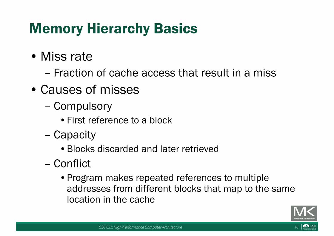
Memory Hierarchy Basics
• Miss rate– Fraction of cache access that result in a miss
• Causes of misses– Compulsory
•First reference to a block– Capacity
•Blocks discarded and later retrieved– Conflict
•Program makes repeated references to multiple addresses from different blocks that map to the same location in the cache
CSC 631: High-Performance Computer Architecture 79
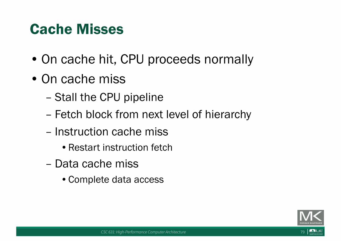
Cache Misses
• On cache hit, CPU proceeds normally• On cache miss
– Stall the CPU pipeline– Fetch block from next level of hierarchy– Instruction cache miss
•Restart instruction fetch
– Data cache miss•Complete data access

CSC 631: High-Performance Computer Architecture 80
Memory Hierarchy Basics
• Note that speculative and multithreaded processors may execute other instructions during a miss– Reduces performance impact of misses

CSC 631: High-Performance Computer Architecture 81
Cache Performance Example
• Given– I-cache miss rate = 2%– D-cache miss rate = 4%– Miss penalty = 100 cycles– Base CPI (ideal cache) = 2– Load & stores are 36% of instructions
• Miss cycles per instruction– I-cache: 0.02 × 100 = 2– D-cache: 0.36 × 0.04 × 100 = 1.44
• Actual CPI = 2 + 2 + 1.44 = 5.44– Ideal CPU is 5.44/2 =2.72 times faster
CSC 631: High-Performance Computer Architecture 82
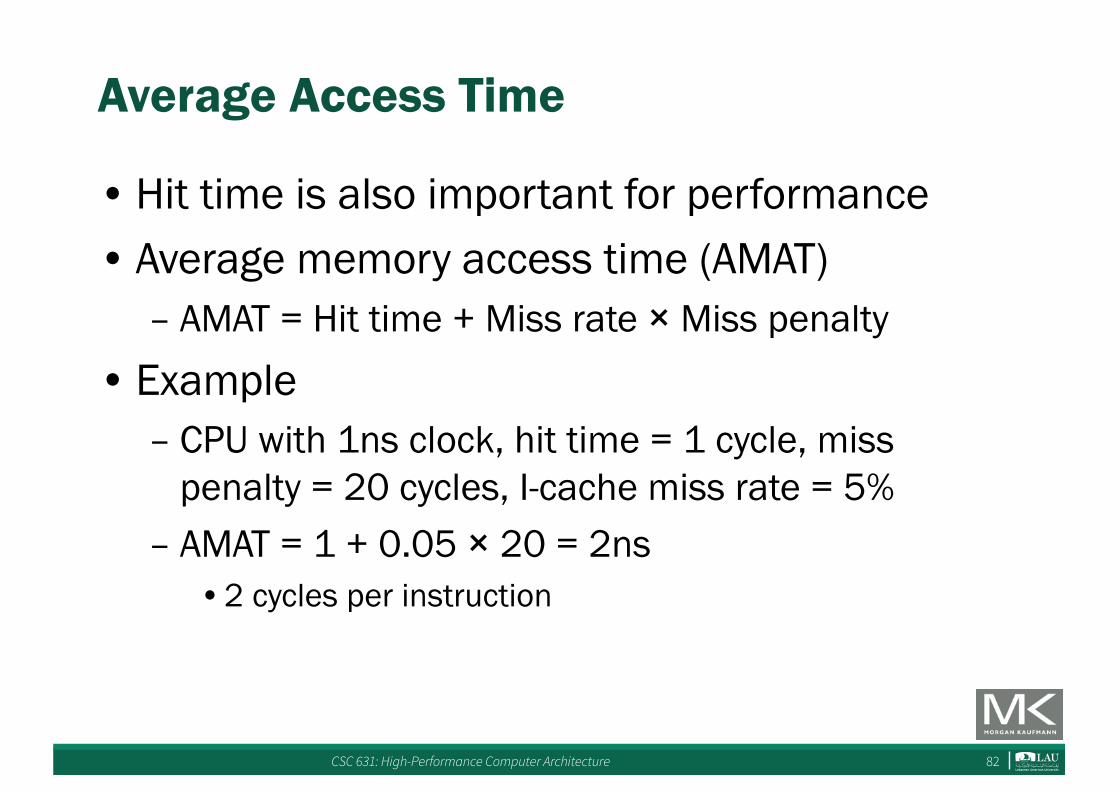
Average Access Time
• Hit time is also important for performance• Average memory access time (AMAT)
– AMAT = Hit time + Miss rate × Miss penalty
• Example– CPU with 1ns clock, hit time = 1 cycle, miss
penalty = 20 cycles, I-cache miss rate = 5%– AMAT = 1 + 0.05 × 20 = 2ns
•2 cycles per instruction
CSC 631: High-Performance Computer Architecture 83
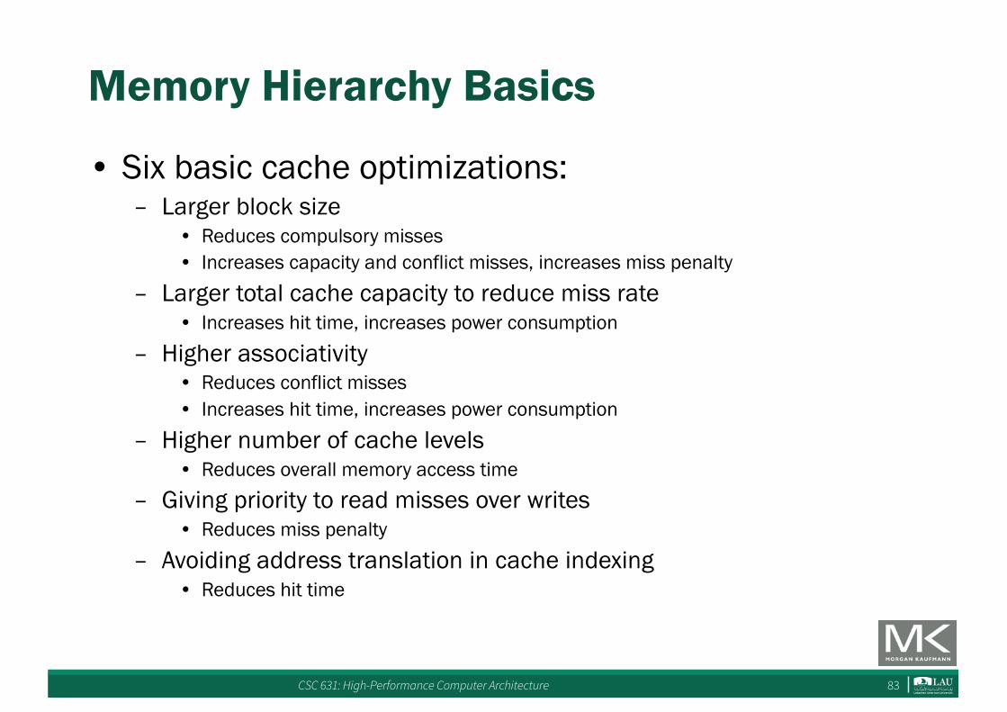
Memory Hierarchy Basics
• Six basic cache optimizations:– Larger block size
• Reduces compulsory misses• Increases capacity and conflict misses, increases miss penalty
– Larger total cache capacity to reduce miss rate• Increases hit time, increases power consumption
– Higher associativity• Reduces conflict misses• Increases hit time, increases power consumption
– Higher number of cache levels• Reduces overall memory access time
– Giving priority to read misses over writes• Reduces miss penalty
– Avoiding address translation in cache indexing• Reduces hit time
CSC 631: High-Performance Computer Architecture 84
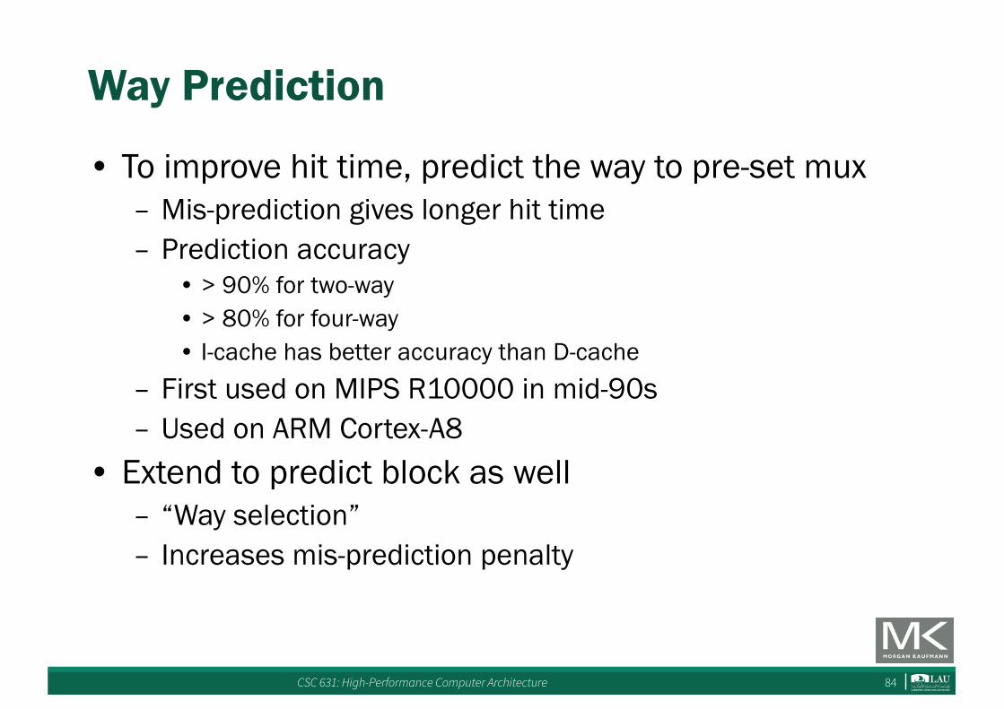
Way Prediction
• To improve hit time, predict the way to pre-set mux– Mis-prediction gives longer hit time– Prediction accuracy
• > 90% for two-way• > 80% for four-way• I-cache has better accuracy than D-cache
– First used on MIPS R10000 in mid-90s– Used on ARM Cortex-A8
• Extend to predict block as well– “Way selection”– Increases mis-prediction penalty

CSC 631: High-Performance Computer Architecture 85
Pipelining Cache
• Pipeline cache access to improve bandwidth– Examples:
• Pentium: 1 cycle• Pentium Pro – Pentium III: 2 cycles• Pentium 4 – Core i7: 4 cycles
• Increases branch mis-prediction penalty• Makes it easier to increase associativity
CSC 631: High-Performance Computer Architecture 86
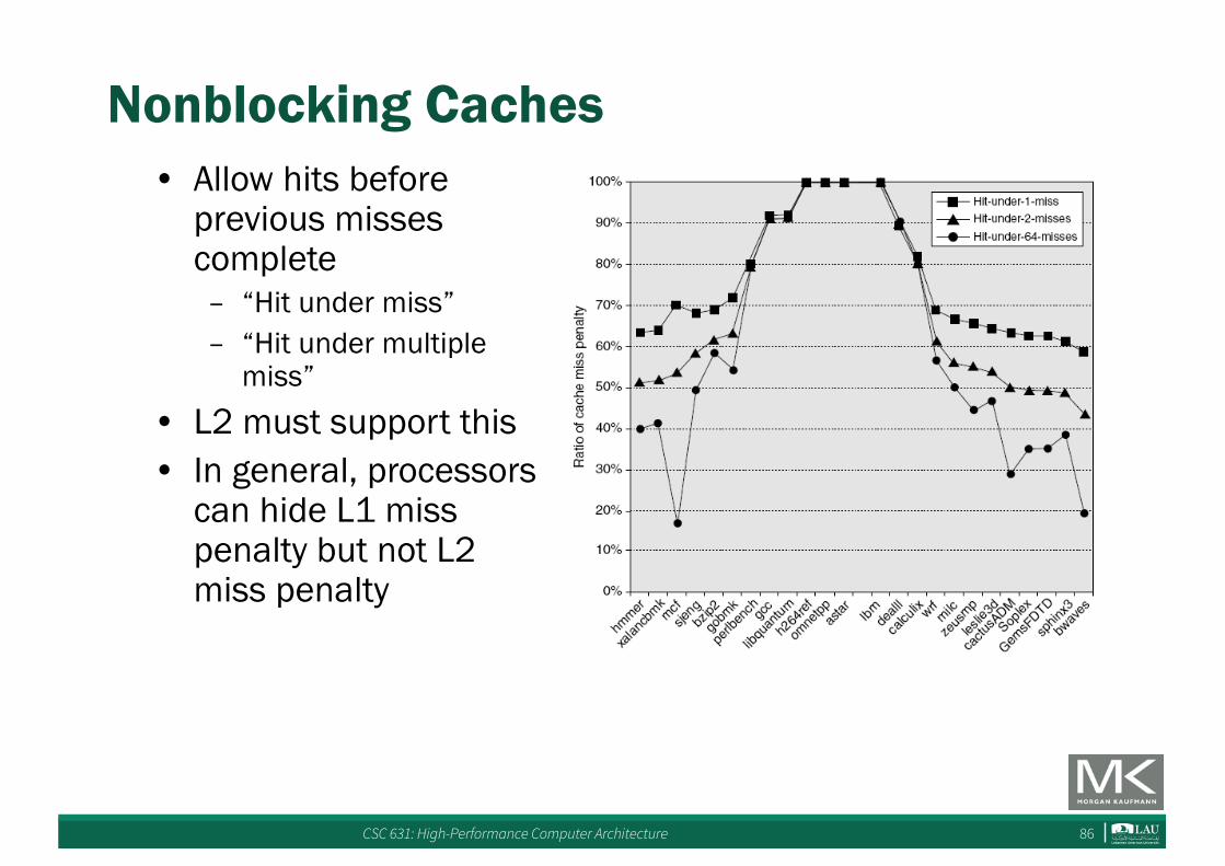
Nonblocking Caches• Allow hits before
previous misses complete– “Hit under miss”– “Hit under multiple
miss”• L2 must support this• In general, processors
can hide L1 miss penalty but not L2 miss penalty

CSC 631: High-Performance Computer Architecture 87
Multibanked Caches• Organize cache as independent banks to
support simultaneous access– ARM Cortex-A8 supports 1-4 banks for L2– Intel i7 supports 4 banks for L1 and 8 banks for L2
• Interleave banks according to block address

CSC 631: High-Performance Computer Architecture 88
Critical Word First, Early Restart• Critical word first
– Request missed word from memory first– Send it to the processor as soon as it arrives
• Early restart– Request words in normal order– Send missed work to the processor as soon as it
arrives
• Effectiveness of these strategies depends on block size and likelihood of another access to the portion of the block that has not yet been fetched
CSC 631: High-Performance Computer Architecture 89
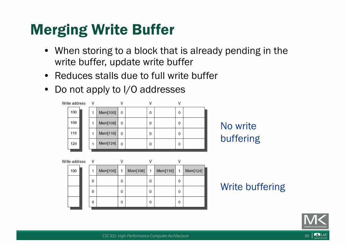
Merging Write Buffer• When storing to a block that is already pending in the
write buffer, update write buffer• Reduces stalls due to full write buffer• Do not apply to I/O addresses
No write buffering
Write buffering

CSC 631: High-Performance Computer Architecture 90
Compiler Optimizations• Loop Interchange
– Swap nested loops to access memory in sequential order
• Blocking– Instead of accessing entire rows or columns,
subdivide matrices into blocks– Requires more memory accesses but improves
locality of accesses

CSC 631: High-Performance Computer Architecture 91
Hardware Prefetching• Fetch two blocks on miss (include next
sequential block)
Pentium 4 Pre-fetching

CSC 631: High-Performance Computer Architecture 92
Compiler Prefetching• Insert prefetch instructions before data is
needed• Non-faulting: prefetch doesn’t cause exceptions
• Register prefetch– Loads data into register
• Cache prefetch– Loads data into cache
• Combine with loop unrolling and software pipelining

CSC 631: High-Performance Computer Architecture 93
Summary
CSC 631: High-Performance Computer Architecture 94
Ten Advanced Optimizations
• Small and simple first level caches– Critical timing path:
• addressing tag memory, then• comparing tags, then• selecting correct set
– Direct-mapped caches can overlap tag compare and transmission of data
– Lower associativity reduces power because fewer cache lines are accessed
CSC 631: High-Performance Computer Architecture 95
Flash Memory• Type of EEPROM• Must be erased (in blocks) before being
overwritten• Non volatile• Limited number of write cycles• Cheaper than SDRAM, more expensive than
disk• Slower than SRAM, faster than disk
CSC 631: High-Performance Computer Architecture 96
Memory Dependability
• Memory is susceptible to cosmic rays• Soft errors: dynamic errors
– Detected and fixed by error correcting codes (ECC)
• Hard errors: permanent errors– Use sparse rows to replace defective rows
• Chipkill: a RAID-like error recovery technique
CSC 631: High-Performance Computer Architecture 97
Virtual Memory
• Protection via virtual memory– Keeps processes in their own memory space
• Role of architecture:– Provide user mode and supervisor mode– Protect certain aspects of CPU state– Provide mechanisms for switching between user
mode and supervisor mode– Provide mechanisms to limit memory accesses– Provide TLB to translate addresses
CSC 631: High-Performance Computer Architecture 98
Virtual Machines
• Supports isolation and security• Sharing a computer among many unrelated
users• Enabled by raw speed of processors, making the
overhead more acceptable• Allows different ISAs and operating systems to be
presented to user programs– “System Virtual Machines”– SVM software is called “virtual machine monitor” or
“hypervisor”– Individual virtual machines run under the monitor are
called “guest VMs”

CSC 631: High-Performance Computer Architecture 99
Impact of VMs on Virtual Memory
• Each guest OS maintains its own set of page tables– VMM adds a level of memory between physical
and virtual memory called “real memory”– VMM maintains shadow page table that maps
guest virtual addresses to physical addresses•Requires VMM to detect guest’s changes to its own
page table•Occurs naturally if accessing the page table pointer is a
privileged operation