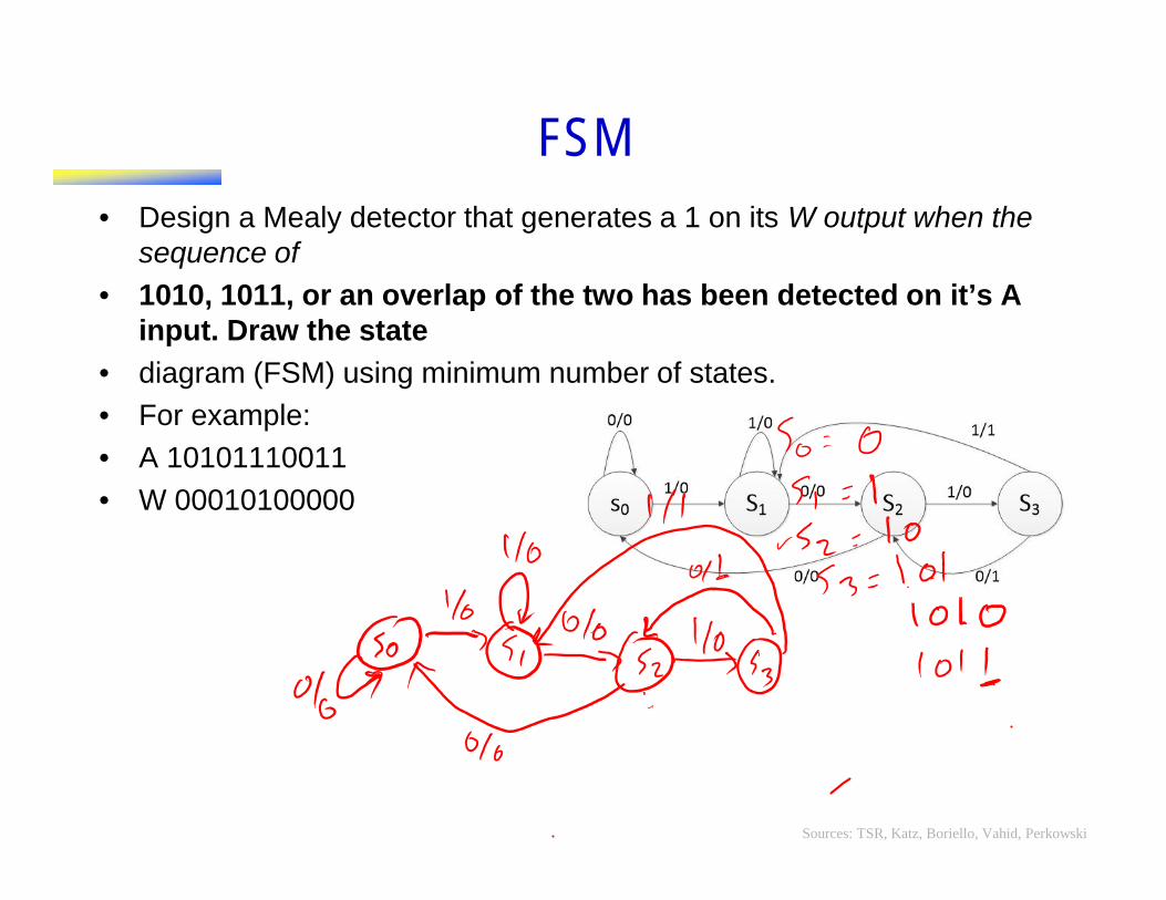
cse140: components and design techniques for digital … · fsm • design a mealy detector that...
TRANSCRIPT

Sources: TSR, Katz, Boriello, Vahid, Perkowski
CSE140: Components and Design Techniquesfor Digital Systems
Review for Final Exam
Mohsen Imani

Sources: TSR, Katz, Boriello, Vahid, Perkowski
CAPE
Please submit your evaluations !!!!

Sources: TSR, Katz, Boriello, Vahid, Perkowski
RTL designUse the RTL design process to design a system that has two 4-bitinputs A and B, and a single output OUT.
When the system samples the input, it will get the value of A if acontrol signal r is 1, B otherwise
The system samples the input and compute the output everyclock cycle when a control signal c is 1. The output is:- The stored input times 2, if the input is lower than a 8-bit input
L.- The stored input divided by 8, otherwise
You can assume that once c is switched to 1, r cannot change itsvalue until c is switched back to 0 first
Assume that once we start sampling values, they are eitheralways greater or always lower than L
Sources: TSR, Katz, Boriello, Vahid, Perkowski
FSM• Design a Mealy detector that generates a 1 on its W output when the
sequence of• 1010, 1011, or an overlap of the two has been detected on it’s A
input. Draw the state• diagram (FSM) using minimum number of states.• For example:• A 10101110011• W 00010100000

Sources: TSR, Katz, Boriello, Vahid, Perkowski
Waveform

Sources: TSR, Katz, Boriello, Vahid, Perkowski
TimingYou are given the RTL circuit below with Full-Adder (FA), a mux and register built from Dflip-flops. The propagation delays of individualcomponents are:• NOT gate = 0.5ns• All other logic gates = 1 ns• Multiplexer delay = 2ns• Clock->Q (D-FF propagation) delay = 2ns.• The setup time for a flip-flop = 15ns.
Assume zero clock skew.
• What is the fastest clock frequency thatthis design can work at ?

Sources: TSR, Katz, Boriello, Vahid, Perkowski
Timingtpcq+tpd+tsetup<Tctpcq = 2nstsetup = 15nstpd = 0.5 + 1 + 3(1) + 2 + 1 + 2= 9.5nsTc > 2 + 15 + 9.5Tc > 26.5nsfc = 1/Tcfc < 1/26.5 GHz

Sources: TSR, Katz, Boriello, Vahid, Perkowski
ALU
label1 =label2=label3=label4=label5=operation1 →operation2 →

Sources: TSR, Katz, Boriello, Vahid, Perkowski
Counter• The counter shown below goes through a repeating sequence
starting from 0000.
(a) How many clock cycles does it take before the sequence repeats?List all the transitions in the sequence
0000 -> 0010 -> 1011 -> 0111 -> 0001 -> 1010 -> 1111 -> 0101 -> 1000 -> 0110 -> 1001-> 1110 -> 1101 -> 1100 -> 0100 -> 0000

Sources: TSR, Katz, Boriello, Vahid, Perkowski
Counter
• Derive a Boolean expression that outputs a logic ‘1’ when a palindrome isdetected on the current value of “WXYZ”. List all palindromes that youobserve in the first 10 transitions of the sequence.
• A palindrome is a string which reads the same in both directions. Forexample,10101 is a palindrome whereas 1100 is not as it is 0011 readbackwards.
• (W XNOR Z) AND (X XNOR Y)• 1111, 0110, 1001

Sources: TSR, Katz, Boriello, Vahid, Perkowski
FSMThe following pattern detector has an input B. Once it detects a pattern,it sets OUT equal to ‘1’. Use the partially filled out state diagram andstate table to do the following:(a) Fill in the missing entries in the state table and complete the FSM.

Sources: TSR, Katz, Boriello, Vahid, Perkowski
FSM Solution• Which pattern is detected by this FSM?

Sources: TSR, Katz, Boriello, Vahid, Perkowski
ALU designUse the previous conf_shifter (configurable shifter) to design anALU that implements the following operations. Operands are 4-bit.
S2 S1 S0 OPERATION000 Bitwise A nor B001 NOT USED010 conf_shift_4(A)011 A + B100 Bitwise A or B101 NOT USED110 conf_shift_2(B)111 B – A
4:1 MUX00 01 10 11
Adder
2:1 MUXOR Conf_shift
AB
0 1
2:1 MUX0 1
2:1 MUX0 1
S2
S2 S2
S2’
S1S0

Sources: TSR, Katz, Boriello, Vahid, Perkowski
Timing constraints
D-FF
D Q
D-FF
D Q
D-FF
D QA[1]
A[0]
S[1]
D-FF
D QC_in
D-FF
D QC_outC_out
D-FF
D Q
D-FF
D Q
B[1]
B[0]
Full Adder
C_out
S
a
b
C_in
FA 100ns 5ns
OR 25ns 10ns
XOR 80ns 70ns
NOT 10ns 10ns
FF
20ns
30ns
10ns
70ns
= 10- Find the maximum
frequency- Check whether there is
a hold violation

Sources: TSR, Katz, Boriello, Vahid, Perkowski
Timing constraints
FA 100ns 5ns
OR 25ns 10ns
XOR 80ns 70ns
NOT 10ns 10ns
FF
20ns
30ns
10ns
70ns
= 10- Find the maximum
frequency- Check whether there is
a hold violation
≥ + + +Where = 10 + 100 + 10 + 25 = 145So = + + + = 20 + 70 + 145 + 10 = 245 nsTherefore = = ∗ 10 Hz ≅ 4Mhz
+ < +Where = 10 + 5 = 15So: 30 + 10 < 10 + 1540 < 25 Hold time violation !!!!!!

Sources: TSR, Katz, Boriello, Vahid, Perkowski
FSMInputs: byte A[256],B[256]
bit go;Output: int sadmain(){
uint sum; short uint i;while (1) {
sum = 0;i = 0;
while (!go);
while (i < 256) {sum = sum + abs(A[i] – B[i]);i = i + 1;
}sad = sum;}
}
go' go
sum:=0i:=0
(i<256)'
i<256
sadreg :=sum
sum:=sum+ abs...
i := i + 1

Sources: TSR, Katz, Boriello, Vahid, Perkowski
Inputs: byte A[256],B[256]bit go;
Output: int sadmain(){
uint sum; short uint i;while (1) {
sum = 0;i = 0;
while (!go);
while (i < 256) {sum = sum + abs(A[i] – B[i]);i = i + 1;
}sad = sum;}
}

Sources: TSR, Katz, Boriello, Vahid, Perkowski
1: HLSM diagram
Init Wait
Input: A (4-bit), B (4-bit), L (8-bit)Output: OUT (5-bit)Local registers: OUTreg (5-bit), INreg (4-bit)
c’
div8_A
div8_B
mult2_A
mult2_B
OUTreg:= 0INreg := 0
OUTreg:= Inreg/8INreg := A
OUTreg:= Inreg/8INreg := B
OUTreg:= Inreg*2INreg := B
OUTreg:= Inreg*2INreg := A
// When not all conditions arereported on transitions, I amassuming that those notreported do not matter

Sources: TSR, Katz, Boriello, Vahid, Perkowski
2.a: DatapathA B
2:1 (4-bit)Mux
OUTreg
>>3<<1
INreg
Compare(<)
2:1 (4-bit)Mux//to thecontroller
ld
clr
ld
clr
ltout_sel
In_sel 10
10
L
Sources: TSR, Katz, Boriello, Vahid, Perkowski
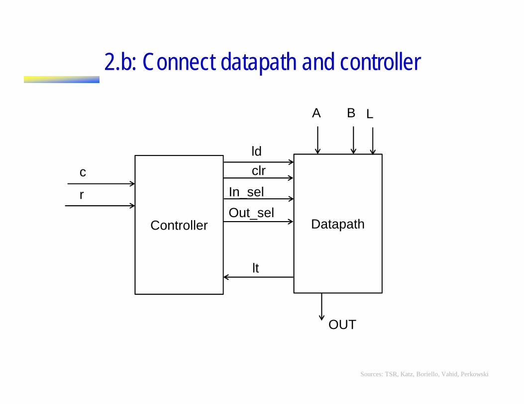
2.b: Connect datapath and controller
DatapathController
c
r
ld
A B
OUT
clrIn_selOut_sel
lt
L

Sources: TSR, Katz, Boriello, Vahid, Perkowski
2.c: Controller FSM
Init Wait
c’
div8_A
div8_B
mult2_A
mult2_B
clr = 1ld = 0
ld = 1In_sel = 0Out_sel = 1
ld = 1In_sel = 1Out_sel = 1
ld = 1In_sel = 0Out_sel = 0
ld = 1In_sel = 1Out_sel = 0

Sources: TSR, Katz, Boriello, Vahid, Perkowski
FSM design 1A FSM has a 1-bit input S and a 2-bit output A[1:0].Initially the output is 00, and it stays at 00 as long as S is 1. If S is0, then the output switches to 01 for only one clock cycle, beforebecoming 10. At this point, if S is 1, then the output will be 00. If Sis 0 instead, the output would remain 10.
S000
S101
SS’
S210
S’
S
SS’

Sources: TSR, Katz, Boriello, Vahid, Perkowski
State and excitation table
S=0 S=1
00 01 00
01 10 10
10 10 00
Q1Q0s D1 D0 A1 A0000 0 1 0 0
001 0 0 0 0
010 1 0 0 1
011 1 0 0 1
100 1 0 1 0
101 0 0 1 0
110 X x x X
111 x X x x
State table with assignment
Excitation table
State assignment:S0: 00S1: 01S2: 10

Sources: TSR, Katz, Boriello, Vahid, Perkowski
Kmaps and equationss\Q1Q0 00 01 11 10
0 0 1 X 1
1 0 1 X 0Q1Q0s D1 D0 A1 A0000 0 1 0 0
001 0 0 0 0
010 1 0 0 1
011 1 0 0 1
100 1 0 1 0
101 0 0 1 0
110 X x x X
111 x X x x
Excitation table
s\Q1Q0 00 01 11 10
0 1 0 X 0
1 0 0 x 0
s\Q1Q0 00 01 11 10
0 0 1 X 0
1 0 1 X 0
s\Q1Q0 00 01 11 10
0 0 0 x 1
1 0 0 X 1
D1 = Q0 + s’Q1D0 = s’Q1’Q0’A1 = Q1A0 = Q0

Sources: TSR, Katz, Boriello, Vahid, Perkowski
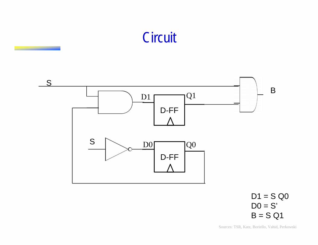
Circuit
D-FFD1 Q1
D-FFD0 Q0
D1 = Q0 + s’Q1D0 = s’Q1’Q0’A1 = Q1A0 = Q0
Q0Q1
s
Q0Q1s
A0
A1

Sources: TSR, Katz, Boriello, Vahid, Perkowski
FSM design 2
Design a Mealy FSM that recognizes the sequence “011”. Themachine has a 1-bit input S and a 1-bit output B. When thesequence is recognized, the output switches to 1 for one clock cycle.
S0 S1 S20/0
1/00/0
1/0
0/0
1/1

Sources: TSR, Katz, Boriello, Vahid, Perkowski
State and excitation table
S=0 S=1
00 01, 0 00, 0
01 01, 0 10, 0
10 01, 0 00, 1
Q1Q0S D1 D0 B
000 0 1 0
001 0 0 0
010 0 1 0
011 1 0 0
100 0 1 0
101 0 0 1
110 x X X
111 x x x
State assignments:S0: 00S1: 01S2: 10
State table with assignment Excitation table

Sources: TSR, Katz, Boriello, Vahid, Perkowski
Kmaps and equationsS\Q1Q0 00 01 11 10
0 0 0 X 0
1 0 1 x 0
S\Q1Q0 00 01 11 10
0 1 1 X 1
1 0 0 x 0
S\Q1Q0 00 01 11 10
0 0 0 X 0
1 0 0 x 1
Q1Q0S D1 D0 B
000 0 1 0
001 0 0 0
010 0 1 0
011 1 0 0
100 0 1 0
101 0 0 1
110 x X X
111 x x x
Excitation table
D1 = S Q0D0 = S’B = S Q1
Sources: TSR, Katz, Boriello, Vahid, Perkowski
Circuit
D1 = S Q0D0 = S’B = S Q1
D-FFD1 Q1
D-FFD0 Q0
B
S
S

Sources: TSR, Katz, Boriello, Vahid, Perkowski
FSM design 3
Starting from the followingcharacteristic equations for aFSM, derive the FSM diagram
D1 = xQ1’Q0
D0 = x’Q1 + Q0
Y = Q1 + Q0’
Is this a Mealy or a Mooremachine? (Moore, becausethe output does not depend onthe input x)
Q1Q0x D1 D0 Y
000 0 1 1
001 0 1 1
010 0 0 0
011 1 1 0
100 0 1 1
101 0 1 1
110 0 0 1
111 0 0 1
Excitation table x=0 x=1
00 01 01
01 00 11
10 01 01
11 00 00
State table withassignment
S0
1
10
S1
S3 S2
0
S0: 00S1: 01S2: 10S3: 11
10
10

Sources: TSR, Katz, Boriello, Vahid, Perkowski
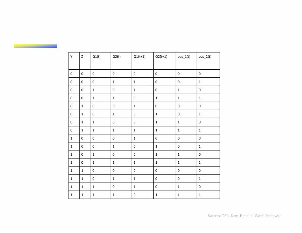
For the given circuit which has two 1 bit inputs (Y, Z) and two outputs(out_1, out_2):a. Write the state table.b. Draw the state diagram.c. Describe the functionality of this FSM.d. Is this a Mealy machine or a Moore machine?
Sources: TSR, Katz, Boriello, Vahid, Perkowski
Y Z Q1(t) Q2(t) Q1(t+1) Q2(t+1) out_1(t) out_2(t)
0 0 0 0 0 0 0 0
0 0 0 1 1 0 0 1
0 0 1 0 1 0 1 0
0 0 1 1 0 1 1 1
0 1 0 0 1 0 0 0
0 1 0 1 0 1 0 1
0 1 1 0 0 1 1 0
0 1 1 1 1 1 1 1
1 0 0 0 1 0 0 0
1 0 0 1 0 1 0 1
1 0 1 0 0 1 1 0
1 0 1 1 1 1 1 1
1 1 0 0 0 0 0 0
1 1 0 1 1 0 0 1
1 1 1 0 1 0 1 0
1 1 1 1 0 1 1 1

Sources: TSR, Katz, Boriello, Vahid, Perkowski
Y Z Current State Next State out_1 out_2
0 0 S0 S0 0 0
0 0 S1 S1 0 1
0 0 S2 S1 1 0
0 0 S3 S2 1 1
0 1 S0 S1 0 0
0 1 S1 S2 0 1
0 1 S2 S2 0 1
0 1 S3 S3 1 1
1 0 S0 S1 0 0
1 0 S1 S2 0 1
1 0 S2 S2 0 1
1 0 S3 S3 1 1
1 1 S0 S0 0 0
1 1 S1 S1 0 1
1 1 S2 S1 1 0
1 1 S3 S2 1 1

Sources: TSR, Katz, Boriello, Vahid, Perkowski

Sources: TSR, Katz, Boriello, Vahid, Perkowski
CSE140 Summary• Transistors and CMOS technology• Boolean algebra• Logic functions, truth tables, circuit representations with basic gates• 2-level logic minimizations using Kmaps• Multiplexers and decoders• ALU components: adders, subtractors (2’s complement representation),
arithmetic shifters, multiplier, dividers.• ALU design• SR latch, level-sensitive SR latch, D-latch, D-FlipFlop• Registers, counters and shift registers• Finite State Machines: Mealy and Moore• Timing Constraints• RTL design

Sources: TSR, Katz, Boriello, Vahid, Perkowski
CSE140 Summary
We can build computers out of one of the simplest mathematical theories(the Boolean algebra) using the simplest numbering system (zeros andones)
We can do that because we have MOS transistors, tiny electronicdevices that are built to provide an extremely simple behavior: beingeither ON or OFF.

Sources: TSR, Katz, Boriello, Vahid, Perkowski
Good Luck for the Final Exam !