current-mode logic (cml) ut65cml8x8fd 3.125 gbps ... · logic (cml) signal i/o pads. the primary...
TRANSCRIPT
Version 2.0.6 1 Cobham Semiconductor Solutions
Cobham.com/HiRel
FEATURES 8 x 8, Full Duplex Crosspoint Switch Matrix
Data Rates up to 3.125 Gbps per Channel
Protocol Independent
Low Propagation Delay (Latency)
Low Channel-to-Channel Skew
SPI Port Control Interface for Ease of Use
Diagnostic Serial Loopback Mode
Low Power Dissipation
Separate Power Domains per Bank
Power Down Feature for Unused Lanes
Loss of Signal (LOS) Detect
Adjustable 50 Ω High-Speed Terminations
Standard Microelectronics Drawing (SMD):
o 5962-17213 (QML-Q, V Pending)
Package Information:
o 143-Pin Ceramic Land Grid Array (C-LGA)
Base Package (Pads Only)
o Ceramic Column Grid Array (C-CGA)
Flight Units
o Ceramic Ball Grid Array (C-BGA)
Prototypes
o Small Size: 14.5 x 14.5 mm; 1 mm Pad Pitch
OPERATIONAL ENVIRONMENT Temperature Range: -55°C to +125°C (MIL Temp.)
Total Dose: 100 kRad (Si)
SEL Immune: ≤ 100 MeV∙cm2/mg
SEU Error Rate: 1.0 x 10⁻¹⁰ errors/bit-day
APPLICATIONS High Speed Serial Repeater and Distribution
Applications
Primary and Redundant Data Switching
Port Replication
Space VPX (VITA78) Data Plane Switches
INTRODUCTION The emerging VITA78, Space VPX, standard specifies a
data plane switch function which enables a redundant and cross strapped serial data path within the VPX
chassis. Typically, a primary serial I/O based resource is cross strapped with a redundant resource. There can
also be redundant resources configured in a non-cross
strapped configuration. This 8 x 8 cross point device can support implementation of either scenario.
Because the switch is purely a cross bar, it is protocol-
independent. This makes the switch very versatile and
can be applied in proprietary architectures, in addition to the Serial Rapid IO protocol specified in VITA78. The
loop back feature, available at each four lane XAUI interface, is very useful for system diagnostics, test, and
optimization.
Two key advantages of the device are its small size and
low power. Any unused lanes can be powered down, and if the device is placed in close proximity to the
source device (e.g. the serial data path is less than 1 or 2 cm), the TX driver can be run in half power mode.
The primary function of the Space VPX 8 x 8 Crosspoint Switch is to perform switching of 10G XAUI serial data
streams between one of two, full duplex, current-mode logic (CML) signal I/O pads. The primary I/O
configuration is an 8 x 8 XAUI-compatible port switch
matrix; each port has four full duplex lanes operating at up to 3.125 Gbps.
Inputs include Receiver (RX) Equalization (EQ) to
compensate for input losses. The input signal is then routed through a MUX to the selected output channel.
Output Transmit (TX) De-Emphasis (DE) is not currently
supported. The Cross Point Switch does not include input Clock and Data Recovery (CDR), and so operates
as a Repeater and not a Re-timer.
The MUX switches which determine the core matrix
configuration are set via the 4-wire SPI register port.
Current-Mode Logic (CML)
UT65CML8X8FD 3.125 Gbps Crosspoint Switch (XPS) Preliminary Datasheet Cobham.com/HiRel July 16, 2018
The most important thing we build is trust

Version 2.0.6 2 Cobham Semiconductor Solutions
Cobham.com/HiRel
1.0 FUNCTIONAL DESCRIPTION
1.1 OVERVIEW
Figure 1 illustrates the functionality of the Crosspoint Switch (XPS). The device is comprised of 4 banks, each
containing 4 individual lanes. Each lane can be individually enabled for transmit only, receive only, or full-duplex operation.
Figure 1: Block Diagram

Version 2.0.6 3 Cobham Semiconductor Solutions
Cobham.com/HiRel
The Crosspoint Switch functionality is illustrated in figures 2 and 3. Individual lanes or groups of lanes within a
bank can be routed directly, as an A-B Crosspoint, or broadcasted to associated banks.
Figure 2: Cross point routing an individual lane
Figure 3: Broadcasting one input bank to two output banks
Version 2.0.6 4 Cobham Semiconductor Solutions
Cobham.com/HiRel
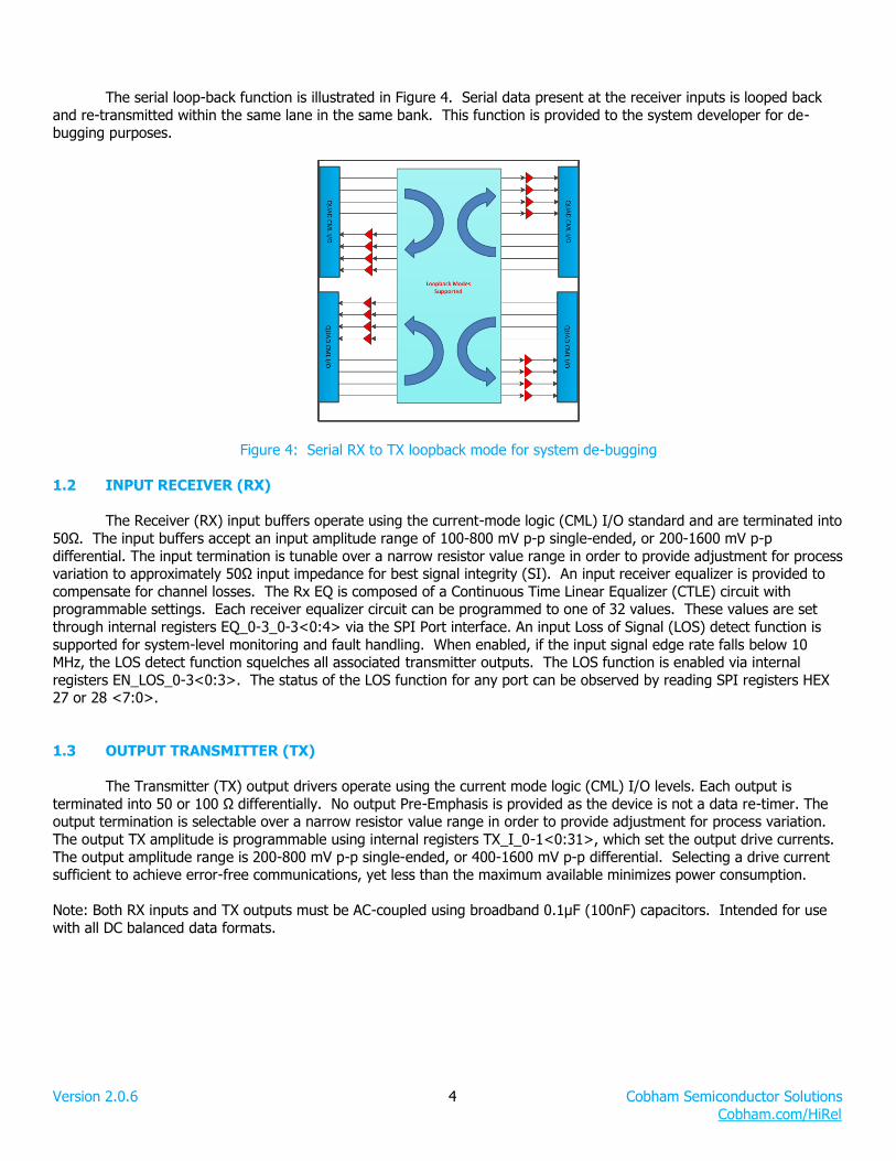
The serial loop-back function is illustrated in Figure 4. Serial data present at the receiver inputs is looped back
and re-transmitted within the same lane in the same bank. This function is provided to the system developer for de-bugging purposes.
Figure 4: Serial RX to TX loopback mode for system de-bugging
1.2 INPUT RECEIVER (RX)
The Receiver (RX) input buffers operate using the current-mode logic (CML) I/O standard and are terminated into
50Ω. The input buffers accept an input amplitude range of 100-800 mV p-p single-ended, or 200-1600 mV p-p
differential. The input termination is tunable over a narrow resistor value range in order to provide adjustment for process variation to approximately 50Ω input impedance for best signal integrity (SI). An input receiver equalizer is provided to
compensate for channel losses. The Rx EQ is composed of a Continuous Time Linear Equalizer (CTLE) circuit with programmable settings. Each receiver equalizer circuit can be programmed to one of 32 values. These values are set
through internal registers EQ_0-3_0-3<0:4> via the SPI Port interface. An input Loss of Signal (LOS) detect function is
supported for system-level monitoring and fault handling. When enabled, if the input signal edge rate falls below 10 MHz, the LOS detect function squelches all associated transmitter outputs. The LOS function is enabled via internal
registers EN_LOS_0-3<0:3>. The status of the LOS function for any port can be observed by reading SPI registers HEX 27 or 28 <7:0>.
1.3 OUTPUT TRANSMITTER (TX)
The Transmitter (TX) output drivers operate using the current mode logic (CML) I/O levels. Each output is
terminated into 50 or 100 Ω differentially. No output Pre-Emphasis is provided as the device is not a data re-timer. The output termination is selectable over a narrow resistor value range in order to provide adjustment for process variation.
The output TX amplitude is programmable using internal registers TX_I_0-1<0:31>, which set the output drive currents.
The output amplitude range is 200-800 mV p-p single-ended, or 400-1600 mV p-p differential. Selecting a drive current sufficient to achieve error-free communications, yet less than the maximum available minimizes power consumption.
Note: Both RX inputs and TX outputs must be AC-coupled using broadband 0.1μF (100nF) capacitors. Intended for use
with all DC balanced data formats.

Version 2.0.6 5 Cobham Semiconductor Solutions
Cobham.com/HiRel
1.4 SERIAL PERIPHERAL INTERFACE (SPI) PORT
1.4.1 OVERVIEW
The Serial Peripheral Interface (SPI) bus is a simple, synchronous, full duplex, 4-wire serial communications
interface in a Master-Slave device configuration. SPI supports single, or multiple slave devices. There is always only one master device. Although there is no formal SPI bus standard, it is widely used, with many variations in existence. Data is
clocked out of the Master device on the MOSI pin to a selected Slave device. One bit is transmitted or received on every SPIclock edge or one byte for eight clock cycles. The SPIcs_n signal is de-asserted to indicate boundaries between
command and data words, or to terminate communication between devices. Because SPI is a primitive protocol, there is no acknowledgement bit (ACK) available. Correct data transmission is verified by reading the selected register byte in
question.
1.4.2 SPI ADVANTAGES
Full duplex communication
Faster data transfer than the I2C or SM bus standards
The flexibility to read and write individual Hexadecimal addresses
Simple hardware interfacing
Slave devices don’t require a unique address
A simple protocol for connecting Master and Slave devices
Tolerant of clock period variation
Serial or parallel configurations allow multiple devices to share the same Master SPI port
1.4.3 SIGNALS
Table 1 lists the Serial Peripheral Interface signals and their directions and functions.
Table 1: SPI Bus Signals
Signal Name Signal Description Signal Direction
SPIclock SPI Serial Clock From Master to Slave device
MOSI Master Out / Slave In From Master to Slave device
MISO Master In / Slave Out From Slave to Master device
SPIcs_n Slave Chip Select, Active Low From Master to Slave device
1.4.4 SPI BUS CONFIGURATIONS
Figure 5a shows a simple point to point SPI configuration. Command and data word operations are conducted in single byte transactions separated by SPIcs_n assertions.
Figure 5a: Master, single slave Point to point configuration
SPIMaster
SPIclock
CS_n
MOS_in
MIS_out
SPISlave
SPIclock
CS_n
MOS_in
MIS_out

Version 2.0.6 6 Cobham Semiconductor Solutions
Cobham.com/HiRel
Figure 5b illustrates multiple parallel Slave devices controlled by a single Master device. While command and
data word operations are conducted in single byte transactions, each Slave device has a unique SPIcs_n selection signal.
Figure 5b: Single master, multiple slaves
Parallel configuration
Figure 5c illustrates multiple serially-connected (i.e. daisy chain) slave devices controlled by a single master
device. Command and data word operations are conducted as a string of serially transmitted, byte-wide transactions. For
N devices connected in serial, N bytes are transmitted back to back. The SPIcs_n signal remains enabled for the duration of multiple command or data word operation. For the example in figure 7, 2 bytes of command or data information are
transmitted with SPIcs_n active. As a result, the Slave FIFOs receive the byte intended for them. Information for the most distant device is transmitted first, the closest last.
Figure 5c: Single master, multiple slaves
Serial configuration

Version 2.0.6 7 Cobham Semiconductor Solutions
Cobham.com/HiRel
1.4.5 SPI INTERFACE RESET
Figure 6 illustrates the SPI port reset and general timing. When the Crosspoint switch is powered, its internal power-on reset (POR) places the SPI port in a reset condition. The user must supply at least 6 clocks to bring
the part out of reset. The chip select signal (SPIcs_n, active low) is asserted at the falling edge of SPIclock ①. In a SPI
transaction, a command word is issued first. Its 7 most significant bits address the control register in question, while the least significant bit indicates whether a read or write operation is requested. A command word follows the data to be
written, or the results of a read, and will be shown in detail in the following sections. Upon completion of a command or
data transaction, two SPI clocks are required to register the transaction. It is important that communication between a Master and Slave device ends with at least one READ of any register. The order and number of READs and WRITEs is not
critical to SPI port operation. SPIclock can and should be stopped after communication is complete.
Figure 6: SPI Reset and General Timing
Command Word
MSB LSB
SPIcs_n
SPIclock
MOS_in
1
3
1 CS_n active at SPIclock falling edge
2 Write / Read_n Control Bit
At least 6 clocks after power-up to
clear the reset
3 2 SPIclocks after CS_n de-asserts
2

Version 2.0.6 8 Cobham Semiconductor Solutions
Cobham.com/HiRel
1.4.6 SPI WRITE
A SPI WRITE operation is shown in Figure 7. The command word LSB indicates a WRITE operation to address Hex 15. The command word LSB (MOS_in), when set to a 1, indicates a WRITE operation. The data word indicates the
data to be written to that location. The chip select SPIcs_n is enabled on the falling edge of SPIclock. After a SPI
interface reset, only one clock is required to begin a SPI transaction. Following a data or command word, 2 clocks are required to completely register a transaction. Data at the MISO output is undefined for WRITE transactions.
Figure 7: SPI Port WRITE operation
Command Word
MSB MSB
LSB
LSB
SPIcs_n
SPIclock
Data Word
Write Control Bit
MOS_in
MIS_out
Undefined During Write
1 2
1 CS_n active at SPIclock falling edge 2 2 SPIclock rising edges after CS_n de-asserts

Version 2.0.6 9 Cobham Semiconductor Solutions
Cobham.com/HiRel
1.4.7 SPI READ
A SPI READ operation is shown in Figure 8. The command word LSB indicates a READ operation from address Hex 15. The command word LSB (MOS_in), when set to a 0, indicates a READ operation. The data word indicates the data to be
read from that location. Following a data or command word, 2 clocks are required to completely register a transaction.
Data transmitted on MISO corresponds to the addressed register value of the previous READ command. The MISO data is transmitted on the negative edge of SPIclock. The first bit is valid data as SPIcs_n is asserted and active at the negative-
edge of the SPIclock
Figure 8: SPI Port READ operation
1.4.8 SPI PORT SAFETY FEATURE
If the number of bits shifted out on the MOSI is not a multiple of 8, the command will be ignored or dropped. If a WRITE
command is a multiple of 8 bits, but the following data word was not, the WRITE command and the data word will be
dropped. In either of these two cases, the WRITE command will need to be re-transmitted.
Read Command Word
MSB MSBLSB LSB
SPIcs_n
SPIclock
Read_n Control Bit Low
MOS_in
MIS_out
Data from the HEX address pointed to in the
previous read command
1 2
1 CS_n active at SPIclock falling edge
2 2 SPIclock rising edges after CS_n de-asserts
Read Command Word
Read_n Control Bit Low
2

Version 2.0.6 10 Cobham Semiconductor Solutions
Cobham.com/HiRel
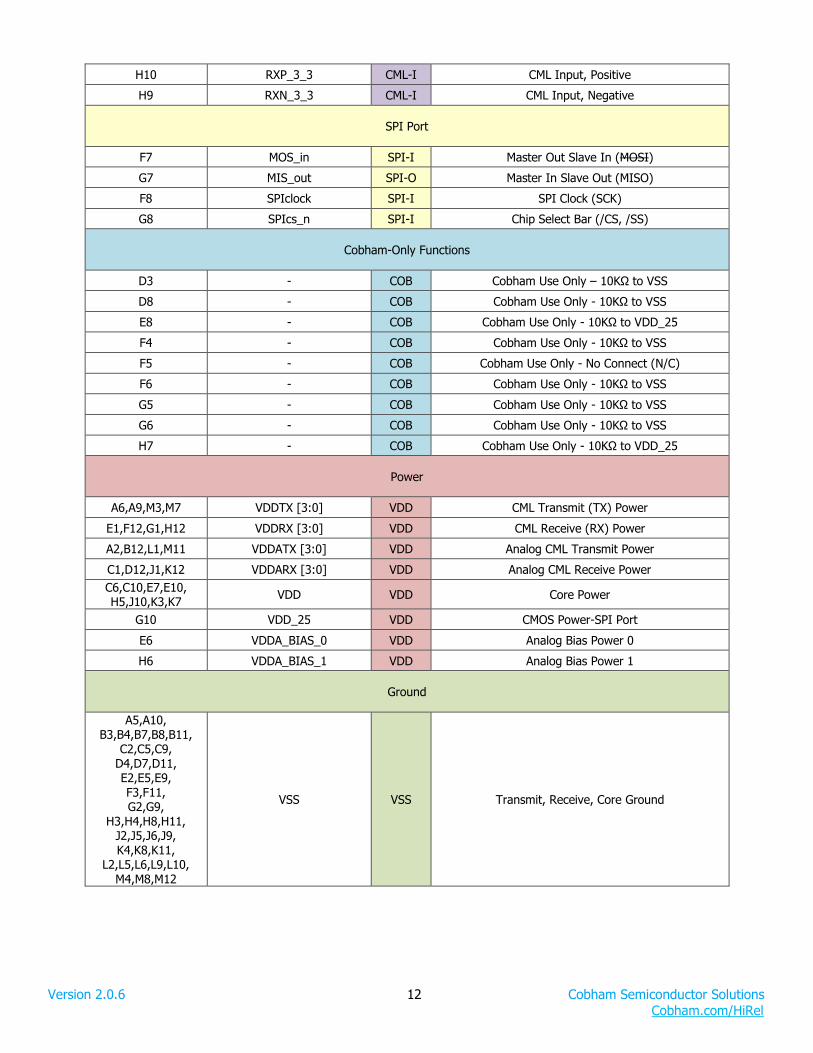
2.0 PINLIST
2.1 PINLIST – TABLE FORMAT
Abbreviation Description
CML-O CML Compatible Output
CML-I CML Compatible Input
SPI-I LVCMOS Compatible Input-SPI Port Only
SPI-O LVCMOS Compatible Output-SPI Port Only
COB Cobham Use Only
VDD Power Supply
VSS Ground
Table 2: Pin list – Table Format
NUMBER NAME TYPE DESCRIPTION
CML Transmitters (TX)
A3 TXP_0_0 CML-O CML Output, Positive
A4 TXN_0_0 CML-O CML Output, Negative
B1 TXP_1_0 CML-O CML Output, Positive
B2 TXN_1_0 CML-O CML Output, Negative
D1 TXP_2_0 CML-O CML Output, Positive
D2 TXN_2_0 CML-O CML Output, Negative
F1 TXP_3_0 CML-O CML Output, Positive
F2 TXN_3_0 CML-O CML Output, Negative
E12 TXP_0_1 CML-O CML Output, Positive
E11 TXN_0_1 CML-O CML Output, Negative
C12 TXP_1_1 CML-O CML Output, Positive
C11 TXN_1_1 CML-O CML Output, Negative
A12 TXP_2_1 CML-O CML Output, Positive
A11 TXN_2_1 CML-O CML Output, Negative
A8 TXP_3_1 CML-O CML Output, Positive
A7 TXN_3_1 CML-O CML Output, Negative
H1 TXP_0_2 CML-O CML Output, Positive
H2 TXN_0_2 CML-O CML Output, Negative
K1 TXP_1_2 CML-O CML Output, Positive
K2 TXN_1_2 CML-O CML Output, Negative
M1 TXP_2_2 CML-O CML Output, Positive
M2 TXN_2_2 CML-O CML Output, Negative
M5 TXP_3_2 CML-O CML Output, Positive
M6 TXN_3_2 CML-O CML Output, Negative

Version 2.0.6 11 Cobham Semiconductor Solutions
Cobham.com/HiRel
M10 TXP_0_3 CML-O CML Output, Positive
M9 TXN_0_3 CML-O CML Output, Negative
L12 TXP_1_3 CML-O CML Output, Positive
L11 TXN_1_3 CML-O CML Output, Negative
J12 TXP_2_3 CML-O CML Output, Positive
J11 TXN_2_3 CML-O CML Output, Negative
G12 TXP_3_3 CML-O CML Output, Positive
G11 TXN_3_3 CML-O CML Output, Negative
CML Receivers (RX)
B6 RXP_0_0 CML-I CML Input, Positive
B5 RXN_0_0 CML-I CML Input, Negative
C3 RXP_1_0 CML-I CML Input, Positive
C4 RXN_1_0 CML-I CML Input, Negative
D5 RXP_2_0 CML-I CML Input, Positive
D6 RXN_2_0 CML-I CML Input, Negative
E3 RXP_3_0 CML-I CML Input, Positive
E4 RXN_3_0 CML-I CML Input, Negative
F10 RXP_0_1 CML-I CML Input, Positive
F9 RXN_0_1 CML-I CML Input, Negative
D10 RXP_1_1 CML-I CML Input, Positive
D9 RXN_1_1 CML-I CML Input, Negative
B10 RXP_2_1 CML-I CML Input, Positive
B9 RXN_2_1 CML-I CML Input, Negative
C8 RXP_3_1 CML-I CML Input, Positive
C7 RXN_3_1 CML-I CML Input, Negative
G3 RXP_0_2 CML-I CML Input, Positive
G4 RXN_0_2 CML-I CML Input, Negative
J3 RXP_1_2 CML-I CML Input, Positive
J4 RXN_1_2 CML-I CML Input, Negative
L3 RXP_2_2 CML-I CML Input, Positive
L4 RXN_2_2 CML-I CML Input, Negative
K5 RXP_3_2 CML-I CML Input, Positive
K6 RXN_3_2 CML-I CML Input, Negative
L8 RXP_0_3 CML-I CML Input, Positive
L7 RXN_0_3 CML-I CML Input, Negative
K10 RXP_1_3 CML-I CML Input, Positive
K9 RXN_1_3 CML-I CML Input, Negative
J8 RXP_2_3 CML-I CML Input, Positive
J7 RXN_2_3 CML-I CML Input, Negative
Version 2.0.6 12 Cobham Semiconductor Solutions
Cobham.com/HiRel
H10 RXP_3_3 CML-I CML Input, Positive
H9 RXN_3_3 CML-I CML Input, Negative
SPI Port
F7 MOS_in SPI-I Master Out Slave In (MOSI)
G7 MIS_out SPI-O Master In Slave Out (MISO)
F8 SPIclock SPI-I SPI Clock (SCK)
G8 SPIcs_n SPI-I Chip Select Bar (/CS, /SS)
Cobham-Only Functions
D3 - COB Cobham Use Only – 10KΩ to VSS
D8 - COB Cobham Use Only - 10KΩ to VSS
E8 - COB Cobham Use Only - 10KΩ to VDD_25
F4 - COB Cobham Use Only - 10KΩ to VSS
F5 - COB Cobham Use Only - No Connect (N/C)
F6 - COB Cobham Use Only - 10KΩ to VSS
G5 - COB Cobham Use Only - 10KΩ to VSS
G6 - COB Cobham Use Only - 10KΩ to VSS
H7 - COB Cobham Use Only - 10KΩ to VDD_25
Power
A6,A9,M3,M7 VDDTX [3:0] VDD CML Transmit (TX) Power
E1,F12,G1,H12 VDDRX [3:0] VDD CML Receive (RX) Power
A2,B12,L1,M11 VDDATX [3:0] VDD Analog CML Transmit Power
C1,D12,J1,K12 VDDARX [3:0] VDD Analog CML Receive Power
C6,C10,E7,E10, H5,J10,K3,K7
VDD VDD Core Power
G10 VDD_25 VDD CMOS Power-SPI Port
E6 VDDA_BIAS_0 VDD Analog Bias Power 0
H6 VDDA_BIAS_1 VDD Analog Bias Power 1
Ground
A5,A10, B3,B4,B7,B8,B11,
C2,C5,C9, D4,D7,D11, E2,E5,E9, F3,F11, G2,G9,
H3,H4,H8,H11, J2,J5,J6,J9, K4,K8,K11,
L2,L5,L6,L9,L10, M4,M8,M12
VSS VSS Transmit, Receive, Core Ground

Version 2.0.6 13 Cobham Semiconductor Solutions
Cobham.com/HiRel
2.2 PINLIST – PACKAGE CONFIGURATION: TOP VIEW
Table 3. Pin List / Package Configuration
12 11 10 9 8 7 6 5 4 3 2 1
M VSS VDDA TX_3
TXP _0_3
TXN _0_3
VSS VDD TX_3
TXN _3_2
TXP _3_2
VSS VDD TX_2
TXN _2_2
TXP _2_2
M
L TXP _1_3
TXN _1_3
VSS VSS RXP _0_3
RXN _0_3
VSS VSS RXN _2_2
RXP _2_2
VSS VDDA TX_2
L
K VDDA RX_3
VSS RXP _1_3
RXN _1_3
VSS VDD RXN _3_2
RXP _3_2
VSS VDD TXN _1_2
TXP _1_2
K
J TXP _2_3
TXN _2_3
VDD VSS RXP _2_3
RXN _2_3
VSS VSS RXN _1_2
RXP _1_2
VSS VDDA RX_2
J
H VDD RX_3
VSS RXP _3_3
RXN _3_3
VSS VDD _25
VDDA _BIAS
_1 VDD VSS VSS
TXN _0_2
TXP _0_2
H
G TXP _3_3
TXN _3_3
VDD _25
VSS SPI cs_n
MIS _out
VSS VSS RXN _0_2
RXP _0_2
VSS VDD RX_2
G
F VDD RX_1
VSS RXP _0_1
RXN _0_1
SPI clock
MOS _in
VSS N/C VSS VSS TXN _3_0
TXP _3_0
F
E TXP _0_1
TXN _0_1
VDD VSS VDD _25
VDD VDDA _BIAS
_0 VSS
RXN _3_0
RXP _3_0
VSS VDD RX_0
E
D VDDA RX_1
VSS RXP _1_1
RXN _1_1
VSS VSS RXN _2_0
RXP _2_0
VSS VSS TXN _2_0
TXP _2_0
D
C TXP _1_1
TXN _1_1
VDD VSS RXP _3_1
RXN _3_1
VDD VSS RXN _1_0
RXP _1_0
VSS VDDA RX_0
C
B VDDA TX_1
VSS RXP _2_1
RXN _2_1
VSS VSS RXP _0_0
RXN _0_0
VSS VSS TXN _1_0
TXP _1_0
B
A TXP _2_1
TXN _2_1
VSS VDD TX_1
TXP _3_1
TXN _3_1
VDD TX_0
VSS TXN _0_0
TXP _0_0
VDDA TX_0
A
12 11 10 9 8 7 6 5 4 3 2 1

Version 2.0.6 14 Cobham Semiconductor Solutions
Cobham.com/HiRel
3.0 ABSOLUTE MAXIMUM RATINGS (1)
Table 4: Absolute Maximum Ratings
SYMBOL PARAMETER MIN MAX UNITS
VDD Core Supply Voltage -0.5 1.40 V
VSS Ground Voltage -0.5 +0.5 V
VDDA_BIAS_0,1 Analog Supply Voltages -0.5 1.40 V
VDDARX Analog CML Receiver (RX) Supply Voltage -0.5 1.40 V
VDDATX Analog CML Transmitter (TX) Supply Voltage -0.5 1.40 V
VDDRX CML Receiver (RX) Supply Voltage -0.5 1.40 V
VDDTX CML Transmitter (TX) Supply Voltage -0.5 2.10 V
VDD_25 SPI Port Supply Voltage -0.5 3.10 V
IOS, LVCMOS LVCMOS Output Short Circuit Current -200 200 mA
VI/O, LVCMOS LVCMOS Input / Output Signal Voltage -0.5 3.10 V
ESDCML CML ESD Rating (HBM) 1 k - V
ESDNON-CML Non-CML ESD Rating (HBM) 2 k - V
PD(PACKAGE)(2) Package Power Dissipation 5.0 W
ӨJC Thermal Resistance (junction to case) 5.0 °C/W
TJ(3) Junction Temperature 150 °C
TSTG Storage Temperature -65 150 °C NOTES:
1. Stresses outside the listed absolute maximum ratings may cause permanent damage to the device. This is a stress rating only and functional operation of the device at these or any other conditions beyond limits indicated in the operational sections of this specification are not recommended. Exposure to absolute maximum rating conditions for extended periods may affect device reliability and performance.
2. Per MIL-STD-883, method 1012.1, section 3.4.1, PD(PACKAGE)=(TJ(max) – TC(max)) / ӨJC 3. Maximum junction temperature (TJ) may be increased to +175°C during burn-in and life test.
4.0 OPERATIONAL ENVIRONMENT
Table 5: Operational Environment
SYMBOL PARAMETER LIMIT UNITS
TID(1) Total Ionizing Dose 1.0E5 rad(Si)
SEL Single Event Latch-up ≤100 MeV∙cm2/mg
SEU(2) Single Event Upset (Error Rate) 1.0x10⁻¹⁰ errors/bit-day NOTES:
1. Irradiated at dose rate = 50 - 300 rads (Si)/s in accordance with MIL-STD-883, method 1019, condition A 2. Adams 90% Geosynchronous orbit
Version 2.0.6 15 Cobham Semiconductor Solutions
Cobham.com/HiRel
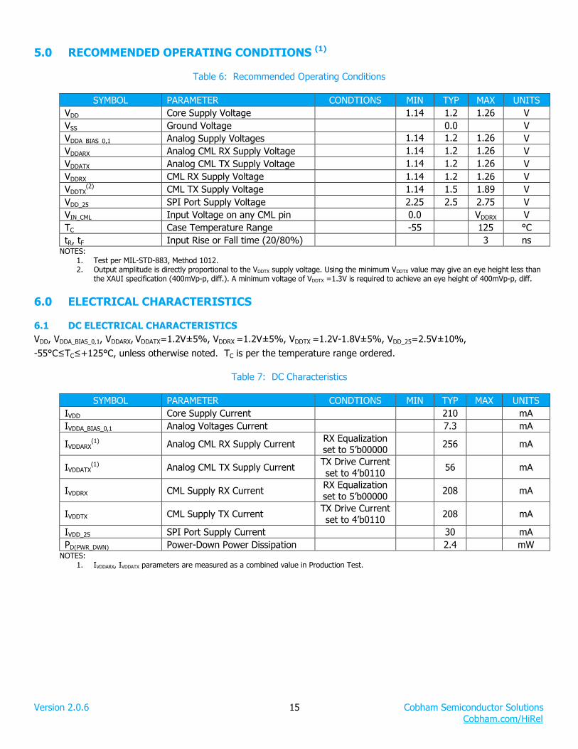
5.0 RECOMMENDED OPERATING CONDITIONS (1)
Table 6: Recommended Operating Conditions
SYMBOL PARAMETER CONDTIONS MIN TYP MAX UNITS
VDD Core Supply Voltage 1.14 1.2 1.26 V
VSS Ground Voltage 0.0 V
VDDA_BIAS_0,1 Analog Supply Voltages 1.14 1.2 1.26 V
VDDARX Analog CML RX Supply Voltage 1.14 1.2 1.26 V
VDDATX Analog CML TX Supply Voltage 1.14 1.2 1.26 V
VDDRX CML RX Supply Voltage 1.14 1.2 1.26 V
VDDTX(2) CML TX Supply Voltage 1.14 1.5 1.89 V
VDD_25 SPI Port Supply Voltage 2.25 2.5 2.75 V
VIN_CML Input Voltage on any CML pin 0.0 VDDRX V
TC Case Temperature Range -55 125 °C
tR, tF Input Rise or Fall time (20/80%) 3 ns NOTES:
1. Test per MIL-STD-883, Method 1012. 2. Output amplitude is directly proportional to the VDDTX supply voltage. Using the minimum VDDTX value may give an eye height less than
the XAUI specification (400mVp-p, diff.). A minimum voltage of VDDTX =1.3V is required to achieve an eye height of 400mVp-p, diff.
6.0 ELECTRICAL CHARACTERISTICS
6.1 DC ELECTRICAL CHARACTERISTICS
VDD, VDDA_BIAS_0,1, VDDARX, VDDATX=1.2V±5%, VDDRX =1.2V±5%, VDDTX =1.2V-1.8V±5%, VDD_25=2.5V±10%,
-55°C≤TC≤+125°C, unless otherwise noted. TC is per the temperature range ordered.
Table 7: DC Characteristics
SYMBOL PARAMETER CONDTIONS MIN TYP MAX UNITS
IVDD Core Supply Current 210 mA
IVDDA_BIAS_0,1 Analog Voltages Current 7.3 mA
IVDDARX(1) Analog CML RX Supply Current
RX Equalization set to 5’b00000
256 mA
IVDDATX(1) Analog CML TX Supply Current
TX Drive Current
set to 4’b0110 56 mA
IVDDRX CML Supply RX Current RX Equalization
set to 5’b00000 208 mA
IVDDTX CML Supply TX Current TX Drive Current set to 4’b0110
208 mA
IVDD_25 SPI Port Supply Current 30 mA
PD(PWR_DWN) Power-Down Power Dissipation 2.4 mW NOTES:
1. IVDDARX, IVDDATX parameters are measured as a combined value in Production Test.

Version 2.0.6 16 Cobham Semiconductor Solutions
Cobham.com/HiRel
6.2 AC ELECTRICAL CHARACTERISTICS
6.2.1 AC ELECTRICAL CHARACTERISTICS: SMALL & LARGE SIGNAL PARAMETERS
VDD, VDDA_BIAS_0,1, VDDARX, VDDATX=1.2V±5%, VDDRX =1.2V±5%, VDDTX =1.2V-1.8V±5%, VDD_25=2.5V±10%,
-55°C≤TC≤+125°C, unless otherwise noted. TC is per the temperature range ordered.
Table 8: AC Characteristics
SYMBOL PARAMETER CONDITIONS MIN TYP MAX UNITS
S11(1) Input Return Loss (RL) <1.0 GHz -10 dB
S22(1) Output Return Loss (RL) < 1.0 GHz -10 dB
VI_CML(2) Input Amplitude, s.e. Single Ended, Peak-to-Peak 100 800 mV
VID_CML Input Amplitude, diff. Differential, Peak-to-Peak 200 1600 mV
VO_CML(2) Output Amplitude, s.e. Single Ended, Peak-to-Peak 200 800 mV
VOD_CML(3) Output Amplitude, diff. Differential, Peak-to-Peak 400 1600 mV
PD(TOTAL) Total Power Dissipation 3.125Gbps, All lanes, Full Duplex,
Medium CML Drive Strength 1.60 W
NOTES: 1. S-parameters: Characterization only. 2. The XPS operation is expected to be by differential signals for the high-speed I/O. Single-ended (s.e.) amplitudes are not measured;
equals one half of the differential amplitude. 3. Output amplitude is directly proportional to the VDDTX supply voltage. Using the minimum VDDTX value may give an eye height less than
the XAUI specification (400mVp-p, diff.). A minimum voltage of VDDTX =1.3V is required to achieve an eye height of 400mVp-p, diff.
6.2.2 AC ELECTRICAL CHARACTERISTICS: TIMING PARAMETERS
VDD, VDDA_BIAS_0,1, VDDARX, VDDATX=1.2V±5%, VDDRX =1.2V±5%, VDDTX =1.2V-1.8V±5%, VDD_25=2.5V±10%,
-55°C≤TC≤+125°C, unless otherwise noted. TC is per the temperature range ordered.
Table 9: Timing Characteristics
SYMBOL PARAMETER CONDITIONS MIN TYP MAX UNITS
DR(1) Data Rate / Channel 0.10 3.125 Gbps
tR, tF(1)
Output Rise / Fall Time Differential, 20% - 80% 140 ps
TJ(1), (2)
Total Jitter 35 90 ps , p-p
fCLK SPI Clock Frequency SPI Port 1 MHz
DCR SPI Clock Duty Cycle Range
SPI Port 40 60 %
tSU,tH Set Up & Hold Time SPI Port 10 ns NOTES:
1. Data Rate (DR), Output rise and fall times (tR, tF), Total Jitter (TJ): Characterization only. 2. Total Jitter (TJ): Best jitter performance is achieved when the receiver equalization is set to 5’b101111.

Version 2.0.6 17 Cobham Semiconductor Solutions
Cobham.com/HiRel
6.3 SPI PORT REGISTER MAP
Table 10: SPI Port Register Map
Name Lane Bank Function Initial
Condition
(1/ 0)
Register
Address
Register
Bit
Reserved 1/0 hex 00 [0:7]
Version Number Design Version Number 1/0 hex 01 [0:6]
POR Flag
Upon reset, this flag will be set to '1'. When this register is
written, this flag will be reset The other registers will be
initialized to their default values.
1 7
Name Lane Bank Function Initial
Condition
(1/ 0)
Register
Address
Register
Bit
RLBS0<0> 0 0 Reverse Loop Back, lane 0, bank 0 0 hex 02 0
RLBS0<1> 1 0 Reverse Loop Back, lane 1, bank 0 0 1
RLBS0<2> 2 0 Reverse Loop Back, lane 2, bank 0 0 2
RLBS0<3> 3 0 Reverse Loop Back, lane 3, bank 0 0 3
RLBS1<0> 0 1 Reverse Loop Back, lane 0, bank 1 0 4
RLBS1<1> 1 1 Reverse Loop Back, lane 1, bank 1 0 5
RLBS1<2> 2 1 Reverse Loop Back, lane 2, bank 1 0 6
RLBS1<3> 3 1 Reverse Loop Back, lane 3, bank 1 0 7
RLBS2<0> 0 2 Reverse Loop Back, lane 0, bank 2 0 hex 03 0
RLBS2<1> 1 2 Reverse Loop Back, lane 1, bank 2 0 1
RLBS2<2> 2 2 Reverse Loop Back, lane 2, bank 2 0 2
RLBS2<3> 3 2 Reverse Loop Back, lane 3, bank 2 0 3
RLBS3<0> 0 3 Reverse Loop Back, lane 0, bank 3 0 4
RLBS3<1> 1 3 Reverse Loop Back, lane 1, bank 3 0 5
RLBS3<2> 2 3 Reverse Loop Back, lane 2, bank 3 0 6
RLBS3<3> 3 3 Reverse Loop Back, lane 3, bank 3 0 7

Version 2.0.6 18 Cobham Semiconductor Solutions
Cobham.com/HiRel
Name Lane Bank Function Initial
Condition
(1/ 0)
Register
Address
Bit
Number
EQ_0_0<0> 0 0 Receiver post equalization, lane 0, bank 0, bit 0 0 hex 04 0
EQ_0_0<1> 0 0 Receiver post equalization, lane 0, bank 0, bit 1 0 1
EQ_0_0<2> 0 0 Receiver post equalization, lane 0, bank 0, bit 2 0 2
EQ_0_0<3> 0 0 Receiver post equalization, lane 0, bank 0, bit 3 1 3
EQ_0_0<4> 0 0 Receiver post equalization, lane 0, bank 0, bit 4 0 4
EQ_0_1<0> 1 0 Receiver post equalization, lane 1, bank 0, bit 0 0 5
EQ_0_1<1> 1 0 Receiver post equalization, lane 1, bank 0, bit 1 0 6
EQ_0_1<2> 1 0 Receiver post equalization, lane 1, bank 0, bit 2 0 7
EQ_0_1<3> 1 0 Receiver post equalization, lane 1, bank 0, bit 3 1 hex 05 0
EQ_0_1<4> 1 0 Receiver post equalization, lane 1, bank 0, bit 4 0 1
EQ_0_2<0> 2 0 Receiver post equalization, lane 2, bank 0, bit 0 0 2
EQ_0_2<1> 2 0 Receiver post equalization, lane 2, bank 0, bit 1 0 3
EQ_0_2<2> 2 0 Receiver post equalization, lane 2, bank 0, bit 2 0 4
EQ_0_2<3> 2 0 Receiver post equalization, lane 2, bank 0, bit 3 1 5
EQ_0_2<4> 2 0 Receiver post equalization, lane 2, bank 0, bit 4 0 6
EQ_0_3<0> 3 0 Receiver post equalization, lane 3, bank 0, bit 0 0 7
EQ_0_3<1> 3 0 Receiver post equalization, lane 3, bank 0, bit 1 0 hex 06 0
EQ_0_3<2> 3 0 Receiver post equalization, lane 3, bank 0, bit 2 0 1
EQ_0_3<3> 3 0 Receiver post equalization, lane 3, bank 0, bit 3 1 2
EQ_0_3<4> 3 0 Receiver post equalization, lane 3, bank 0, bit 4 0 3
EQ_1_0<0> 0 1 Receiver post equalization, lane 0, bank 1, bit 0 0 4
EQ_1_0<1> 0 1 Receiver post equalization, lane 0, bank 1, bit 1 0 5
EQ_1_0<2> 0 1 Receiver post equalization, lane 0, bank 1, bit 2 0 6
EQ_1_0<3> 0 1 Receiver post equalization, lane 0, bank 1, bit 3 1 7
EQ_1_0<4> 0 1 Receiver post equalization, lane 0, bank 1, bit 4 0 hex 07 0
EQ_1_1<0> 1 1 Receiver post equalization, lane 1, bank 1, bit 0 0 1
EQ_1_1<1> 1 1 Receiver post equalization, lane 1, bank 1, bit 1 0 2
EQ_1_1<2> 1 1 Receiver post equalization, lane 1, bank 1, bit 2 0 3
EQ_1_1<3> 1 1 Receiver post equalization, lane 1, bank 1, bit 3 1 4
EQ_1_1<4> 1 1 Receiver post equalization, lane 1, bank 1, bit 4 0 5
EQ_1_2<0> 2 1 Receiver post equalization, lane 2, bank 1, bit 0 0 6
EQ_1_2<1> 2 1 Receiver post equalization, lane 2, bank 1, bit 1 0 7
EQ_1_2<2> 2 1 Receiver post equalization, lane 2, bank1 , bit 2 0 hex 08 0
EQ_1_2<3> 2 1 Receiver post equalization, lane 2, bank 1, bit 3 1 1
EQ_1_2<4> 2 1 Receiver post equalization, lane 2, bank 1, bit 4 0 2
EQ_1_3<0> 3 1 Receiver post equalization, lane 3, bank 1, bit 0 0 3
EQ_1_3<1> 3 1 Receiver post equalization, lane 3, bank 1, bit 1 0 4
EQ_1_3<2> 3 1 Receiver post equalization, lane 3, bank 1, bit 2 0 5
EQ_1_3<3> 3 1 Receiver post equalization, lane 3, bank 1, bit 3 1 6
EQ_1_3<4> 3 1 Receiver post equalization, lane 3, bank 1, bit 4 0 7
EQ_2_0<0> 0 2 Receiver post equalization, lane 0, bank 2, bit 0 0 hex 09 0
EQ_2_0<1> 0 2 Receiver post equalization, lane 0, bank 2, bit 1 0 1
EQ_2_0<2> 0 2 Receiver post equalization, lane 0, bank 2, bit 2 0 2
EQ_2_0<3> 0 2 Receiver post equalization, lane 0, bank 2, bit 3 1 3
EQ_2_0<4> 0 2 Receiver post equalization, lane 0, bank 2, bit 4 0 4
EQ_2_1<0> 1 2 Receiver post equalization, lane 1, bank 2, bit 0 0 5
EQ_2_1<1> 1 2 Receiver post equalization, lane 1, bank 2, bit 1 0 6
EQ_2_1<2> 1 2 Receiver post equalization, lane 1, bank 2, bit 2 0 7
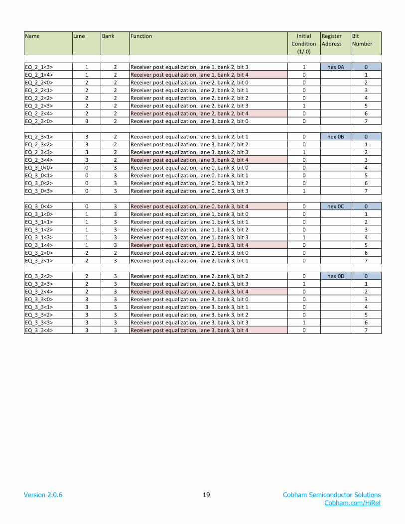
Version 2.0.6 19 Cobham Semiconductor Solutions
Cobham.com/HiRel
Name Lane Bank Function Initial
Condition
(1/ 0)
Register
Address
Bit
Number
EQ_2_1<3> 1 2 Receiver post equalization, lane 1, bank 2, bit 3 1 hex 0A 0
EQ_2_1<4> 1 2 Receiver post equalization, lane 1, bank 2, bit 4 0 1
EQ_2_2<0> 2 2 Receiver post equalization, lane 2, bank 2, bit 0 0 2
EQ_2_2<1> 2 2 Receiver post equalization, lane 2, bank 2, bit 1 0 3
EQ_2_2<2> 2 2 Receiver post equalization, lane 2, bank 2, bit 2 0 4
EQ_2_2<3> 2 2 Receiver post equalization, lane 2, bank 2, bit 3 1 5
EQ_2_2<4> 2 2 Receiver post equalization, lane 2, bank 2, bit 4 0 6
EQ_2_3<0> 3 2 Receiver post equalization, lane 3, bank 2, bit 0 0 7
EQ_2_3<1> 3 2 Receiver post equalization, lane 3, bank 2, bit 1 0 hex 0B 0
EQ_2_3<2> 3 2 Receiver post equalization, lane 3, bank 2, bit 2 0 1
EQ_2_3<3> 3 2 Receiver post equalization, lane 3, bank 2, bit 3 1 2
EQ_2_3<4> 3 2 Receiver post equalization, lane 3, bank 2, bit 4 0 3
EQ_3_0<0> 0 3 Receiver post equalization, lane 0, bank 3, bit 0 0 4
EQ_3_0<1> 0 3 Receiver post equalization, lane 0, bank 3, bit 1 0 5
EQ_3_0<2> 0 3 Receiver post equalization, lane 0, bank 3, bit 2 0 6
EQ_3_0<3> 0 3 Receiver post equalization, lane 0, bank 3, bit 3 1 7
EQ_3_0<4> 0 3 Receiver post equalization, lane 0, bank 3, bit 4 0 hex 0C 0
EQ_3_1<0> 1 3 Receiver post equalization, lane 1, bank 3, bit 0 0 1
EQ_3_1<1> 1 3 Receiver post equalization, lane 1, bank 3, bit 1 0 2
EQ_3_1<2> 1 3 Receiver post equalization, lane 1, bank 3, bit 2 0 3
EQ_3_1<3> 1 3 Receiver post equalization, lane 1, bank 3, bit 3 1 4
EQ_3_1<4> 1 3 Receiver post equalization, lane 1, bank 3, bit 4 0 5
EQ_3_2<0> 2 2 Receiver post equalization, lane 2, bank 3, bit 0 0 6
EQ_3_2<1> 2 3 Receiver post equalization, lane 2, bank 3, bit 1 0 7
EQ_3_2<2> 2 3 Receiver post equalization, lane 2, bank 3, bit 2 0 hex 0D 0
EQ_3_2<3> 2 3 Receiver post equalization, lane 2, bank 3, bit 3 1 1
EQ_3_2<4> 2 3 Receiver post equalization, lane 2, bank 3, bit 4 0 2
EQ_3_3<0> 3 3 Receiver post equalization, lane 3, bank 3, bit 0 0 3
EQ_3_3<1> 3 3 Receiver post equalization, lane 3, bank 3, bit 1 0 4
EQ_3_3<2> 3 3 Receiver post equalization, lane 3, bank 3, bit 2 0 5
EQ_3_3<3> 3 3 Receiver post equalization, lane 3, bank 3, bit 3 1 6
EQ_3_3<4> 3 3 Receiver post equalization, lane 3, bank 3, bit 4 0 7

Version 2.0.6 20 Cobham Semiconductor Solutions
Cobham.com/HiRel
Name Lane Bank Function Initial
Condition
(1/ 0)
Register
Address
Register
Bit
PD_rx_0<0> 0 0 Receiver Power Down lane 0, bank 0 0 hex 0E 0
PD_rx_0<1> 1 0 Receiver Power Down lane 1, bank 0 0 1
PD_rx_0<2> 2 0 Receiver Power Down lane 2, bank 0 0 2
PD_rx_0<3> 3 0 Receiver Power Down lane 3, bank 0 0 3
PD_rx_1<0> 0 1 Receiver Power Down lane 0, bank 1 0 4
PD_rx_1<1> 1 1 Receiver Power Down lane 1, bank 1 0 5
PD_rx_1<2> 2 1 Receiver Power Down lane 2, bank 1 0 6
PD_rx_1<3> 3 1 Receiver Power Down lane 3, bank 1 0 7
PD_rx_2<0> 0 2 Receiver Power Down lane 0, bank 2 0 hex 0F 0
PD_rx_2<1> 1 2 Receiver Power Down lane 1, bank 2 0 1
PD_rx_2<2> 2 2 Receiver Power Down lane 2, bank 2 0 2
PD_rx_2<3> 3 2 Receiver Power Down lane 3, bank 2 0 3
PD_rx_3<0> 0 3 Receiver Power Down lane 0, bank 3 0 4
PD_rx_3<1> 1 3 Receiver Power Down lane 1, bank 3 0 5
PD_rx_3<2> 2 3 Receiver Power Down lane 2, bank 3 0 6
PD_rx_3<3> 3 3 Receiver Power Down lane 3, bank 3 0 7
Name Lane Bank Function Initial
Condition
(1/ 0)
Register
Address
Bit
Number
HI_Z_TX_0<0> 0 0 Transmitter termination High Z, lane 0, bank 0 0 hex 10 0
HI_Z_TX_0<1> 1 0 Transmitter termination High Z, lane 1, bank 0 0 1
HI_Z_TX_0<2> 2 0 Transmitter termination High Z, lane 2, bank 0 0 2
HI_Z_TX_0<3> 3 0 Transmitter termination High Z, lane 3, bank 0 0 3
HI_Z_TX_0<4> 0 1 Transmitter termination High Z, lane 0, bank 1 0 4
HI_Z_TX_0<5> 1 1 Transmitter termination High Z, lane 1, bank 1 0 5
HI_Z_TX_0<6> 2 1 Transmitter termination High Z, lane 2, bank 1 0 6
HI_Z_TX_0<7> 3 1 Transmitter termination High Z, lane 3, bank 1 0 7
HI_Z_TX_1<0> 0 2 Transmitter termination High Z, lane 0, bank 2 0 hex 11 0
HI_Z_TX_1<1> 1 2 Transmitter termination High Z, lane 1, bank 2 0 1
HI_Z_TX_1<2> 2 2 Transmitter termination High Z, lane 2, bank 2 0 2
HI_Z_TX_1<3> 3 2 Transmitter termination High Z, lane 3, bank 2 0 3
HI_Z_TX_1<4> 0 3 Transmitter termination High Z, lane 0, bank 3 0 4
HI_Z_TX_1<5> 1 3 Transmitter termination High Z, lane 1, bank 3 0 5
HI_Z_TX_1<6> 2 3 Transmitter termination High Z, lane 2, bank 3 0 6
HI_Z_TX_1<7> 3 3 Transmitter termination High Z, lane 3, bank 3 0 7
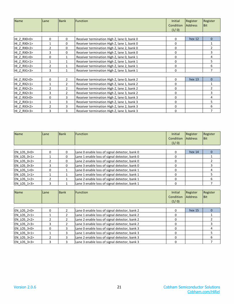
Version 2.0.6 21 Cobham Semiconductor Solutions
Cobham.com/HiRel
Name Lane Bank Function Initial
Condition
(1/ 0)
Register
Address
Register
Bit
HI_Z_RX0<0> 0 0 Receiver termination High Z, lane 0, bank 0 0 hex 12 0
HI_Z_RX0<1> 1 0 Receiver termination High Z, lane 1, bank 0 0 1
HI_Z_RX0<2> 2 0 Receiver termination High Z, lane 2, bank 0 0 2
HI_Z_RX0<3> 3 0 Receiver termination High Z, lane 3, bank 0 0 3
HI_Z_RX1<0> 0 1 Receiver termination High Z, lane 0, bank 1 0 4
HI_Z_RX1<1> 1 1 Receiver termination High Z, lane 1, bank 1 0 5
HI_Z_RX1<2> 2 1 Receiver termination High Z, lane 2, bank 1 0 6
HI_Z_RX1<3> 3 1 Receiver termination High Z, lane 3, bank 1 0 7
HI_Z_RX2<0> 0 2 Receiver termination High Z, lane 0, bank 2 0 hex 13 0
HI_Z_RX2<1> 1 2 Receiver termination High Z, lane 1, bank 2 0 1
HI_Z_RX2<2> 2 2 Receiver termination High Z, lane 2, bank 2 0 2
HI_Z_RX2<3> 3 2 Receiver termination High Z, lane 3, bank 2 0 3
HI_Z_RX3<0> 0 3 Receiver termination High Z, lane 0, bank 3 0 4
HI_Z_RX3<1> 1 3 Receiver termination High Z, lane 1, bank 3 0 5
HI_Z_RX3<2> 2 3 Receiver termination High Z, lane 2, bank 3 0 6
HI_Z_RX3<3> 3 3 Receiver termination High Z, lane 3, bank 3 0 7
Name Lane Bank Function Initial
Condition
(1/ 0)
Register
Address
Register
Bit
EN_LOS_0<0> 0 0 Lane 0 enable loss of signal detector, bank 0 0 hex 14 0
EN_LOS_0<1> 1 0 Lane 1 enable loss of signal detector, bank 0 0 1
EN_LOS_0<2> 2 0 Lane 2 enable loss of signal detector, bank 0 0 2
EN_LOS_0<3> 3 0 Lane 3 enable loss of signal detector, bank 0 0 3
EN_LOS_1<0> 0 1 Lane 0 enable loss of signal detector, bank 1 0 4
EN_LOS_1<1> 1 1 Lane 1 enable loss of signal detector, bank 1 0 5
EN_LOS_1<2> 2 1 Lane 2 enable loss of signal detector, bank 1 0 6
EN_LOS_1<3> 3 1 Lane 3 enable loss of signal detector, bank 1 0 7
Name Lane Bank Function Initial
Condition
(1/ 0)
Register
Address
Register
Bit
EN_LOS_2<0> 0 2 Lane 0 enable loss of signal detector, bank 2 0 hex 15 0
EN_LOS_2<1> 1 2 Lane 1 enable loss of signal detector, bank 2 0 1
EN_LOS_2<2> 2 2 Lane 2 enable loss of signal detector, bank 2 0 2
EN_LOS_2<3> 3 2 Lane 3 enable loss of signal detector, bank 2 0 3
EN_LOS_3<0> 0 3 Lane 0 enable loss of signal detector, bank 3 0 4
EN_LOS_3<1> 1 3 Lane 1 enable loss of signal detector, bank 3 0 5
EN_LOS_3<2> 2 3 Lane 2 enable loss of signal detector, bank 3 0 6
EN_LOS_3<3> 3 3 Lane 3 enable loss of signal detector, bank 3 0 7

Version 2.0.6 22 Cobham Semiconductor Solutions
Cobham.com/HiRel
Name Lane Bank Function Initial
Condition
(1/ 0)
Register
Address
Register
Bit
TX_I_0<0> 0 0 Lane 0 transmitter drive current, bank 0, bit 0 0 hex 16 0
TX_I_0<1> 0 0 Lane 0 transmitter drive current, bank 0, bit 1 0 1
TX_I_0<2> 0 0 Lane 0 transmitter drive current, bank 0, bit 2 0 2
TX_I_0<3> 0 0 Lane 0 transmitter drive current, bank 0, bit 3 1 3
TX_I_0<4> 1 0 Lane 1 transmitter drive current, bank 0, bit 0 0 4
TX_I_0<5> 1 0 Lane 1 transmitter drive current, bank 0, bit 1 0 5
TX_I_0<6> 1 0 Lane 1 transmitter drive current, bank 0, bit 2 0 6
TX_I_0<7> 1 0 Lane 1 transmitter drive current, bank 0, bit 3 1 7
TX_I_0<8> 2 0 Lane 2 transmitter drive current, bank 0, bit 0 0 hex 17 0
TX_I_0<9> 2 0 Lane 2 transmitter drive current, bank 0, bit 1 0 1
TX_I_0<10> 2 0 Lane 2 transmitter drive current, bank 0, bit 2 0 2
TX_I_0<11> 2 0 Lane 2 transmitter drive current, bank 0, bit 3 1 3
TX_I_0<12> 3 0 Lane 3 transmitter drive current, bank 0, bit 0 0 4
TX_I_0<13> 3 0 Lane 3 transmitter drive current, bank 0, bit 1 0 5
TX_I_0<14> 3 0 Lane 3 transmitter drive current, bank 0, bit 2 0 6
TX_I_0<15> 3 0 Lane 3 transmitter drive current, bank 0, bit 3 1 7
TX_I_0<16> 0 1 Lane 0 transmitter drive current, bank 1, bit 0 0 hex 18 0
TX_I_0<17> 0 1 Lane 0 transmitter drive current, bank 1, bit 1 0 1
TX_I_0<18> 0 1 Lane 0 transmitter drive current, bank 1, bit 2 0 2
TX_I_0<19> 0 1 Lane 0 transmitter drive current, bank 1, bit 3 1 3
TX_I_0<20> 1 1 Lane 1 transmitter drive current, bank 1, bit 0 0 4
TX_I_0<21> 1 1 Lane 1 transmitter drive current, bank 1, bit 1 0 5
TX_I_0<22> 1 1 Lane 1 transmitter drive current, bank 1, bit 2 0 6
TX_I_0<23> 1 1 Lane 1 transmitter drive current, bank 1, bit 3 1 7
TX_I_0<24> 2 1 Lane 2 transmitter drive current, bank 1, bit 0 0 hex 19 0
TX_I_0<25> 2 1 Lane 2 transmitter drive current, bank 1, bit 1 0 1
TX_I_0<26> 2 1 Lane 2 transmitter drive current, bank 1, bit 2 0 2
TX_I_0<27> 2 1 Lane 2 transmitter drive current, bank 1, bit 3 1 3
TX_I_0<28> 3 1 Lane 3 transmitter drive current, bank 1, bit 0 0 4
TX_I_0<29> 3 1 Lane 3 transmitter drive current, bank 1, bit 1 0 5
TX_I_0<30> 3 1 Lane 3 transmitter drive current, bank 1, bit 2 0 6
TX_I_0<31> 3 1 Lane 3 transmitter drive current, bank 1, bit 3 1 7
TX_I_1<0> 0 2 Lane 0 transmitter drive current, bank 2, bit 0 0 hex 1A 0
TX_I_1<1> 0 2 Lane 0 transmitter drive current, bank 2, bit 1 0 1
TX_I_1<2> 0 2 Lane 0 transmitter drive current, bank 2, bit 2 0 2
TX_I_1<3> 0 2 Lane 0 transmitter drive current, bank 2, bit 3 1 3
TX_I_1<4> 1 2 Lane 1 transmitter drive current, bank 2, bit 0 0 4
TX_I_1<5> 1 2 Lane 1 transmitter drive current, bank 2, bit 1 0 5
TX_I_1<6> 1 2 Lane 1 transmitter drive current, bank 2, bit 2 0 6
TX_I_1<7> 1 2 Lane 1 transmitter drive current, bank 2, bit 3 1 7
TX_I_1<8> 2 2 Lane 2 transmitter drive current, bank 2, bit 0 0 hex 1B 0
TX_I_1<9> 2 2 Lane 2 transmitter drive current, bank 2, bit 1 0 1
TX_I_1<10> 2 2 Lane 2 transmitter drive current, bank 2, bit 2 0 2
TX_I_1<11> 2 2 Lane 2 transmitter drive current, bank 2, bit 3 1 3
TX_I_1<12> 3 2 Lane 3 transmitter drive current, bank 2, bit 0 0 4
TX_I_1<13> 3 2 Lane 3 transmitter drive current, bank 2, bit 1 0 5
TX_I_1<14> 3 2 Lane 3 transmitter drive current, bank 2, bit 2 0 6
TX_I_1<15> 3 2 Lane 3 transmitter drive current, bank 2, bit 3 1 7

Version 2.0.6 23 Cobham Semiconductor Solutions
Cobham.com/HiRel
Name Lane Bank Function Initial
Condition
(1/ 0)
Register
Address
Register
Bit
TX_I_1<16> 0 3 Lane 0 transmitter drive current, bank 3, bit 0 0 hex 1C 0
TX_I_1<17> 0 3 Lane 0 transmitter drive current, bank 3, bit 1 0 1
TX_I_1<18> 0 3 Lane 0 transmitter drive current, bank 3, bit 2 0 2
TX_I_1<19> 0 3 Lane 0 transmitter drive current, bank 3, bit 3 1 3
TX_I_1<20> 1 3 Lane 1 transmitter drive current, bank 3, bit 0 0 4
TX_I_1<21> 1 3 Lane 1 transmitter drive current, bank 3, bit 1 0 5
TX_I_1<22> 1 3 Lane 1 transmitter drive current, bank 3, bit 2 0 6
TX_I_1<23> 1 3 Lane 1 transmitter drive current, bank 3, bit 3 1 7
TX_I_1<24> 2 3 Lane 2 transmitter drive current, bank 3, bit 0 0 hex 1D 0
TX_I_1<25> 2 3 Lane 2 transmitter drive current, bank 3, bit 1 0 1
TX_I_1<26> 2 3 Lane 2 transmitter drive current, bank 3, bit 2 0 2
TX_I_1<27> 2 3 Lane 2 transmitter drive current, bank 3, bit 3 1 3
TX_I_1<28> 3 3 Lane 3 transmitter drive current, bank 3, bit 0 0 4
TX_I_1<29> 3 3 Lane 3 transmitter drive current, bank 3, bit 1 0 5
TX_I_1<30> 3 3 Lane 3 transmitter drive current, bank 3, bit 2 0 6
TX_I_1<31> 3 3 Lane 3 transmitter drive current, bank 3, bit 3 1 7
Name Lane Bank Function Initial
Condition
(1/ 0)
Register
Address
Register
Bit
PD_TX_0<0> 0 0 Power down transmitter, lane 0, bank 0 0 hex 1E 0
PD_TX_0<1> 1 0 Power down transmitter, lane 1, bank 0 0 1
PD_TX_0<2> 2 0 Power down transmitter, lane 2, bank 0 0 2
PD_TX_0<3> 3 0 Power down transmitter, lane 3, bank 0 0 3
PD_TX_0<4> 0 1 Power down transmitter, lane 0, bank 1 0 4
PD_TX_0<5> 1 1 Power down transmitter, lane 1, bank 1 0 5
PD_TX_0<6> 2 1 Power down transmitter, lane 2, bank 1 0 6
PD_TX_0<7> 3 1 Power down transmitter, lane 3, bank 1 0 7
PD_TX_1<0> 0 2 Power down transmitter, lane 0, bank 2 0 hex 1F 0
PD_TX_1<1> 1 2 Power down transmitter, lane 1, bank 2 0 1
PD_TX_1<2> 2 2 Power down transmitter, lane 2, bank 2 0 2
PD_TX_1<3> 3 2 Power down transmitter, lane 3, bank 2 0 3
PD_TX_1<4> 0 3 Power down transmitter, lane 0, bank 3 0 4
PD_TX_1<5> 1 3 Power down transmitter, lane 1, bank 3 0 5
PD_TX_1<6> 2 3 Power down transmitter, lane 2, bank 3 0 6
PD_TX_1<7> 3 3 Power down transmitter, lane 3, bank 3 0 7

Version 2.0.6 24 Cobham Semiconductor Solutions
Cobham.com/HiRel
Name Lane Bank Function Initial
Condition
(1/ 0)
Register
Address
Register
Bit
PDR0<0> 0 0 Power down receiver bias current, lane 0, bank 0 0 hex 20 0
PDR0<1> 1 0 Power down receiver bias current, lane 1, bank 0 0 1
PDR0<2> 2 0 Power down receiver bias current, lane 2, bank 0 0 2
PDR0<3> 3 0 Power down receiver bias current, lane 3, bank 0 0 3
PDR0<4> 0 1 Power down receiver bias current, lane 0, bank 1 0 4
PDR0<5> 1 1 Power down receiver bias current, lane 1, bank 1 0 5
PDR0<6> 2 1 Power down receiver bias current, lane 2, bank 1 0 6
PDR0<7> 3 1 Power down receiver bias current, lane 3, bank 1 0 7
Name Lane Bank Function Initial
Condition
(1/ 0)
Register
Address
Register
Bit
PDR1<0> 0 2 Power down receiver bias current, lane 0, bank 2 0 hex 21 0
PDR1<1> 1 2 Power down receiver bias current, lane 1, bank 2 0 1
PDR1<2> 2 2 Power down receiver bias current, lane 2, bank 2 0 2
PDR1<3> 3 2 Power down receiver bias current, lane 3, bank 2 0 3
PDR1<4> 0 3 Power down receiver bias current, lane 0, bank 3 0 4
PDR1<5> 1 3 Power down receiver bias current, lane 1, bank 3 0 5
PDR1<6> 2 3 Power down receiver bias current, lane 2, bank 3 0 6
PDR1<7> 3 3 Power down receiver bias current, lane 3, bank 3 0 7
Name Lane Bank Function Initial
Condition
(1/ 0)
Register
Address
Register
Bit
S_ab0<0> 0 0 Multiplexer control, side a to side b, lane 0, bank 0 0 hex 22 0
S_ab0<1> 1 0 Multiplexer control, side a to side b, lane 1, bank 0 0 1
S_ab0<2> 2 0 Multiplexer control, side a to side b, lane 2, bank 0 0 2
S_ab0<3> 3 0 Multiplexer control, side a to side b, lane 3, bank 0 0 3
S_ab1<0> 0 1 Multiplexer control, side a to side b, lane 0, bank 1 0 4
S_ab1<1> 1 1 Multiplexer control, side a to side b, lane 1, bank 1 0 5
S_ab1<2> 2 1 Multiplexer control, side a to side b, lane 2, bank 1 0 6
S_ab1<3> 3 1 Multiplexer control, side a to side b, lane 3, bank 1 0 7
Name Lane Bank Function Initial
Condition
(1/ 0)
Register
Address
Register
Bit
S_ba2<0> 0 2 Multiplexer control, side b to side a, lane 0, bank 2 0 hex 23 0
S_ba2<1> 1 2 Multiplexer control, side b to side a, lane 1, bank 2 0 1
S_ba2<2> 2 2 Multiplexer control, side b to side a, lane 2, bank 2 0 2
S_ba2<3> 3 2 Multiplexer control, side b to side a, lane 3, bank 2 0 3
S_ba3<0> 0 3 Multiplexer control, side b to side a, lane 0, bank 3 0 4
S_ba3<1> 1 3 Multiplexer control, side b to side a, lane 1, bank 3 0 5
S_ba3<2> 2 3 Multiplexer control, side b to side a, lane 2, bank 3 0 6
S_ba3<3> 3 3 Multiplexer control, side b to side a, lane 3, bank 3 0 7
Version 2.0.6 25 Cobham Semiconductor Solutions
Cobham.com/HiRel
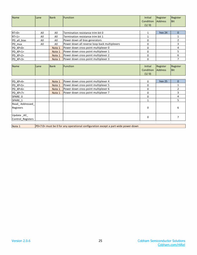
Name Lane Bank Function Initial
Condition
(1/ 0)
Register
Address
Register
Bit
RT<0> All All Termination resistance trim bit 0 1 hex 24 0
RT<1> All All Termination resistance trim bit 1 1 1
PD_all_bias All All Power down all bias generators 0 2
PD_mux All All Power down all reverse loop back multiplexers 0 3
PD_XP<0> Note 1 Power down cross point multiplexer 0 0 4
PD_XP<1> Note 1 Power down cross point multiplexer 1 0 5
PD_XP<2> Note 1 Power down cross point multiplexer 2 0 6
PD_XP<3> Note 1 Power down cross point multiplexer 3 0 7
Name Lane Bank Function Initial
Condition
(1/ 0)
Register
Address
Register
Bit
PD_XP<4> Note 1 Power down cross point multiplexer 4 0 hex 25 0
PD_XP<5> Note 1 Power down cross point multiplexer 5 0 1
PD_XP<6> Note 1 Power down cross point multiplexer 6 0 2
PD_XP<7> Note 1 Power down cross point multiplexer 7 0 3
SPARE_0 0 4
SPARE_1 1 5
Read_ Addressed_
Registers 0 6
Update _All_
Control_Registers0 7
Note 1 PD<7:0> must be 0 for any operational configuration except a part-wide power-down

Version 2.0.6 26 Cobham Semiconductor Solutions
Cobham.com/HiRel
Name Lane Bank Function Initial
Condition
(1/ 0)
Register
Address
Register
Bit
SPARE_2 Unused 1 hex 26 0
SPARE_3 Unused 0 1
SPARE_4 Unused 1 2
SPARE_5 Unused 0 3
SPARE_6 Unused 1 4
SPARE_7 Unused 0 5
SPARE_8 Unused 1 6
SPARE_9 Unused 0 7
Name Lane Bank Function Initial
Condition
(1/ 0)
Register
Address
Register
Bit
LOS_0<0> 0 0 Status of Loss of Signal, Read Only hex 27 0
LOS_0<1> 1 0 Status of Loss of Signal, Read Only 1
LOS_0<2> 2 0 Status of Loss of Signal, Read Only 2
LOS_0<3> 3 0 Status of Loss of Signal, Read Only 3
LOS_1<0> 0 1 Status of Loss of Signal, Read Only 4
LOS_1<1> 1 1 Status of Loss of Signal, Read Only 5
LOS_1<2> 2 1 Status of Loss of Signal, Read Only 6
LOS_1<3> 3 1 Status of Loss of Signal, Read Only 7
Name Lane Bank Function Initial
Condition
(1/ 0)
Register
Address
Register
Bit
LOS_2<0> 0 2 Status of Loss of Signal, Read Only hex 28 0
LOS_2<1> 1 2 Status of Loss of Signal, Read Only 1
LOS_2<2> 2 2 Status of Loss of Signal, Read Only 2
LOS_2<3> 3 2 Status of Loss of Signal, Read Only 3
LOS_3<0> 0 3 Status of Loss of Signal, Read Only 4
LOS_3<1> 1 3 Status of Loss of Signal, Read Only 5
LOS_3<2> 2 3 Status of Loss of Signal, Read Only 6
LOS_3<3> 3 3 Status of Loss of Signal, Read Only 7

Version 2.0.6 27 Cobham Semiconductor Solutions
Cobham.com/HiRel
7.0 PACKAGE DRAWINGS
Figure 9a: 143 Land, Ceramic Land Grid Array (CLGA)

Version 2.0.6 28 Cobham Semiconductor Solutions
Cobham.com/HiRel
7.0 PACKAGE DRAWINGS (CONTINUED)
Figure 9b: 143 Ball, Ceramic Ball Grid Array (CBGA) Notes: (1) Solder balls are available for prototypes and engineering samples only, as they are not QML-qualified. (2) The dimensions shown for the attached solder balls are approximate.

Version 2.0.6 29 Cobham Semiconductor Solutions
Cobham.com/HiRel
7.0 PACKAGE DRAWINGS (CONTINUED)
Figure 9c: 143 Column, Ceramic Column Grid Array (CCGA)

Version 2.0.6 30 Cobham Semiconductor Solutions
Cobham.com/HiRel
Table11: Package Dimensions (mm)
SYMBOL Millimeters (mm)
Min Typ Max
A2 4.2164
A3 0.65
D 14.50
D1 11.00
e 1.00
E 13.70
E1 11.00
R 0.25
S 0.50
LID 0.127
Version 2.0.6 31 Cobham Semiconductor Solutions
Cobham.com/HiRel
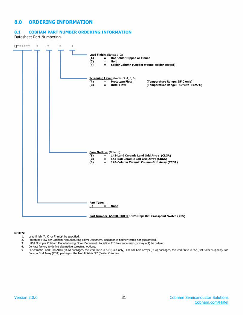
8.0 ORDERING INFORMATION
8.1 COBHAM PART NUMBER ORDERING INFORMATION Datasheet Part Numbering
UT***** * * * *
NOTES:
1. Lead finish (A, C, or F) must be specified. 2. Prototype Flow per Cobham Manufacturing Flows Document. Radiation is neither tested nor guaranteed.
3. HiRel Flow per Cobham Manufacturing Flows Document. Radiation TID tolerance may (or may not) be ordered. 4. Contact factory to define alternative screening options.
5. For ceramic Land Grid Array (LGA) packages, the lead finish is “C” (Gold-only). For Ball Grid Arrays (BGA) packages, the lead finish is “A” (Hot Solder Dipped). For Column Grid Array (CGA) packages, the lead finish is “F” (Solder Column).
Lead Finish: (Notes: 1, 2) (A) = Hot Solder Dipped or Tinned
(C) = Gold (F) = Solder Column (Copper wound, solder coated)
Screening Level: (Notes: 3, 4, 5, 6) (P) = Prototype Flow (Temperature Range: 25°C only)
(C) = HiRel Flow (Temperature Range: -55°C to +125°C)
Case Outline: (Note: 8) (Z) = 143-Land Ceramic Land Grid Array (CLGA)
(C) = 143-Ball Ceramic Ball Grid Array (CBGA) (S) = 143-Column Ceramic Column Grid Array (CCGA)
Part Type: (-) = None
Part Number: 65CML8X8FD 3.125 Gbps 8x8 Crosspoint Switch (XPS)

Version 2.0.6 32 Cobham Semiconductor Solutions
Cobham.com/HiRel
8.2 SMD PART NUMBER ORDERING INFORMATION SMD Part Numbering
5962 * 17213 ** * * * NOTES:
1. Lead finish must be specified. Part marking will reflect the lead finish applied to the device shipped. 2. For ceramic Land Grid Array (LGA) packages, the lead finish is “C” (Gold-only). For Ball Grid Arrays (BGA) packages, the lead finish is “A” (Hot Solder Dipped). For
Column Grid Array (CGA) packages, the lead finish is “F” (Solder Column). 3. Contact factory to determine alternative screening options. 4. A radiation hardness assurance level must be selected. The use of “-” indicates no radiation hardness assurance guarantee.
5. Device type 01 is irradiated at dose rate = 50 – 300 rad(Si)/s in accordance with MIL-STD-883, method 1019, condition A, and is guaranteed to a maximum total dose specified. The effective dose rate after extended room temperature anneal = 1 rad(Si)/s per MIL-STD-883, method 1019, condition A, section 3.11.2. The
total dose specification for these devices only applies to the specified effective dose rate, or lower, environment.
Lead Finish: (Notes: 1) (A) = Hot Solder Dipped or Tinned
(C) = Gold (F) = Solder Column (Copper wound, solder coated)
Case Outline: (Note: 2) (X) = Ceramic Land Grid Array (CLGA) (Y) = Ceramic Column Grid Array (CCGA)
QML/JAN Class: (Note: 3)
(Q) = Class Q (V) = Class V
Device Type:
(01) = UT65CML8X8FD (Temperature Range: -55°C to +125°C)
SMD Project Number: (17213) = 3.125 Gbps 8x8 Crosspoint Switch (XPS)
Radiation Hardness Assurance: (Notes: 4, 5) (R) = 100 krad(Si)
Federal Stock Class Designator

Version 2.0.6 33 Cobham Semiconductor Solutions
Cobham.com/HiRel
9.0 REVISION HISTORY
Date Revision Change Description
2017/11/01 2.0.0 Advanced Datasheet – Draft – Correction to Ordering Info., pp. 31,32.
2018/03/21 2.0.1 Advanced Datasheet – Draft – Edits for uniform header size
2018/03/22 2.0.2 Advanced Datasheet – Draft – Updates to Electrical Tables 4,6,7,8
2018/04/10 2.0.3 Advanced Datasheet – Draft – Update to Table 5: Added SEU parameter, + foratting
2018/04/12 2.0.4 Adv. D.S., Draft: 1.4.6,7-SPI; 3,5,6.2.1-PD, Tables 4,6,8; 6.1-MAXtoTYP, Table 7
2018/04/17 2.0.5 Adv. D.S., Draft: 6.1, Table 7; 6.2.1, Table 8; 6.2.2 Table 9: Notes updated
2018/07/16 2.0.6 Adv. D.S. to Prelim. D.S.

Version 2.0.6 34 Cobham Semiconductor Solutions
Cobham.com/HiRel
Cobham Semiconductor Solutions – Datasheet Definitions
Advanced Datasheet - Product In Development
Preliminary Datasheet - Shipping Prototype
Released Datasheet - Shipping QML & Reduced Hi – Rel
The following United States (U.S.) Department of Commerce statement shall be applicable if these commodities, technology, or software are exported from the U.S.: These commodities, technology, or software were exported from the
United States in accordance with the Export Administration Regulations. Diversion contrary to U.S. law is prohibited.
Cobham Semiconductor Solutions
4350 Centennial Blvd Colorado Springs, CO 80907
T: 800 645 8862
Aeroflex Colorado Springs Inc., dba Cobham Semiconductor Solutions, reserves the right to make changes to any products and services described herein at any time without notice. Consult Aeroflex or an authorized sales representative to verify that the information in this data sheet is current before using this product. Aeroflex does not assume any responsibility or liability arising out of the application or use of any product or service described herein, except as expressly agreed to in writing by Aeroflex; nor does the purchase, lease, or use of a product or service from Aeroflex convey a license under any patent rights, copyrights, trademark rights, or any other of the intellectual rights of Aeroflex or of third parties.