custom ic blocks for enabling digital control in switching ... · custom ic blocks for enabling...
TRANSCRIPT

CoPEC
1July 11, 2003
Custom IC Blocks for Enabling Digital Control in
Switching Power Converters
Dragan Maksimovic and Regan Zane
July 11, 2003
Colorado Power Electronics CenterUniversity of Colorado, Boulder

CoPEC
2July 11, 2003
Outline
• Motivations & CoPEC directions• “Buffalo switcher”
– Complete 1 MHz digital PWM controller IC– Hybrid digital PWM– Delay-line A/D
• CoPEC research highlights• Education:
– focus on power electronics & mixed-signal IC design
CoPEC
3July 11, 2003
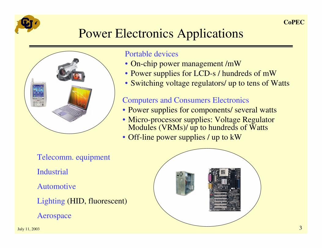
Power Electronics ApplicationsPortable devices • On-chip power management /mW• Power supplies for LCD-s / hundreds of mW• Switching voltage regulators/ up to tens of Watts
Computers and Consumers Electronics • Power supplies for components/ several watts• Micro-processor supplies: Voltage Regulator
Modules (VRMs)/ up to hundreds of Watts • Off-line power supplies / up to kW
Telecomm. equipment
Industrial
Automotive
Lighting (HID, fluorescent)
Aerospace

CoPEC
4July 11, 2003
ProcessingCore
BatteryBatteryMonitorBatteryMonitor
Li-IonProtectorLi-Ion
ProtectorBattery
Management
AudioCodec
AudioCodec
Audio PwrAmp
Audio PwrAmp
Color or B/W LCDwith Touchscreen
TouchscreenControl
TouchscreenControl
FrontlightWhite LED
Supply VoltageSupervisor
Supply VoltageSupervisor
Alkaline
BatteryChargerBatteryCharger
Power Management
BoostConverter
BoostConverter
BuckConverter
BuckConverter
ChargePump
ChargePump
Low-DropoutRegulator
Low-DropoutRegulator
Buck-BoostConverter
Buck-BoostConverter
MicrophoneAmp
MicrophoneAmp
SDRAMSRAMFLASHROM
LogicBus Drvr
Li+ Ni+
BacklightCCFL
CCFL CtrlCCFL Ctrl
Wall SupplyUSB Power
MemoryExpansion
PowerSwitchPowerSwitch
3.3V / 5VSystem Supply
1.5 / 1.8V / 2.5VCore Supply
Wireless I/F
Wired I/F
Microphone
LoudspeakerHeadphonesWireless
Ethernet802.11b
WirelessAccess
Bluetooth
USB
PDA Example: Power Management

CoPEC
5July 11, 2003
Buck Switching Converter Example
• Switching operation controls the average value of vD
• LC low-pass filter reduces the voltage ripple in the dc output Vout
• High switching frequency (hundreds of kHz to MHz), small size• Ideally lossless, very high efficiency in practice• Tightly regulated Vout through a feedback loop
Vinswitchingconverter Load
Vout
Vref
pulse widthmodulator
-compensator
d(t)
Controller+ +e(t)
Control
inout DVV =Duty ratio
M L
C LoadVout
+
Vin vD
+
_
-state
DTsTs
ON OFF
t
M
vD(t)Vin
Power Processing

CoPEC
6July 11, 2003
Controller Implementation: Analog vs. Digital
Hvout(t)
D
M L
C R
vout +
-
H
+
-
driver
Vref
error amplifierand compensator
comparator
-+
Analog controller
Ts
+Vin
saw-toothwaveformgenerator
t
VM
vc(t)+-e(t)
H
D
M L
C R
vout+
+
-
A/D
Compensatord[n]=f{d[n-1], d[n-2],..,e[n],e[n-1]..}
DPWMHvout(t)
Hvout[n]
Digital Controller
e[n]+
Vref[n]
+
-
Vin
driver
d[n]
Analog Implementation Digital Implementation
CoPEC
7July 11, 2003
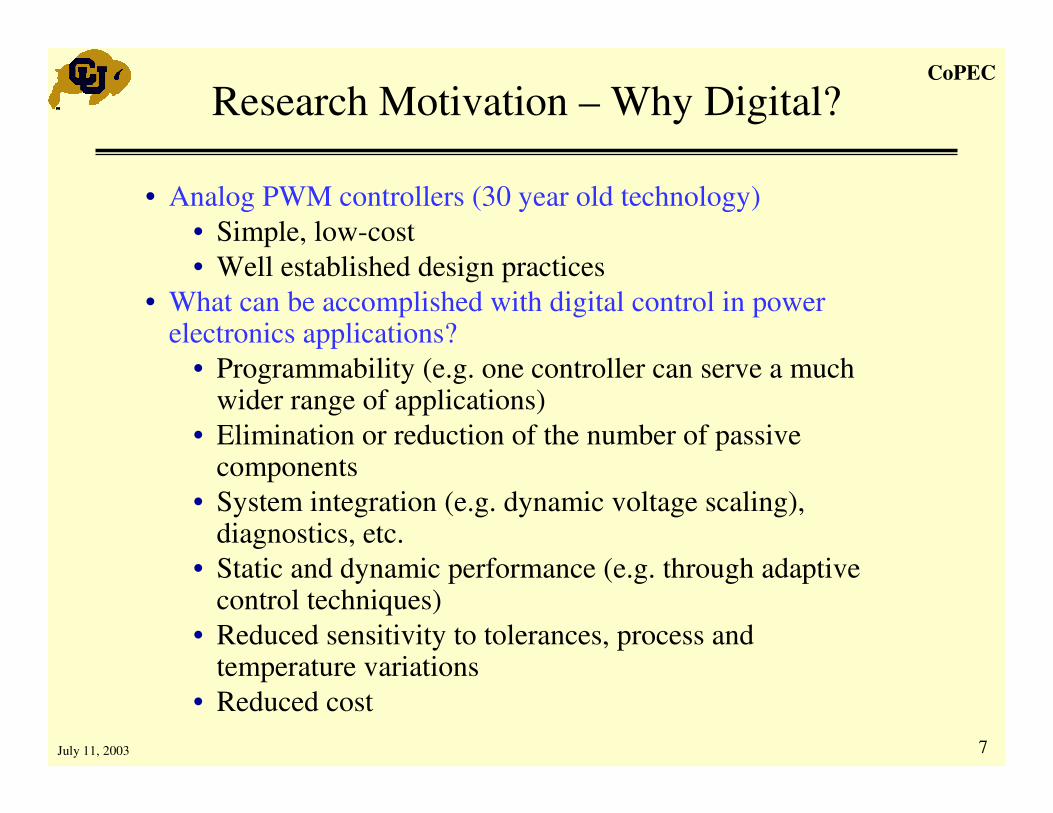
Research Motivation – Why Digital?
• Analog PWM controllers (30 year old technology)• Simple, low-cost• Well established design practices
• What can be accomplished with digital control in power electronics applications?
• Programmability (e.g. one controller can serve a much wider range of applications)
• Elimination or reduction of the number of passive components
• System integration (e.g. dynamic voltage scaling), diagnostics, etc.
• Static and dynamic performance (e.g. through adaptive control techniques)
• Reduced sensitivity to tolerances, process and temperature variations
• Reduced cost
CoPEC
8July 11, 2003
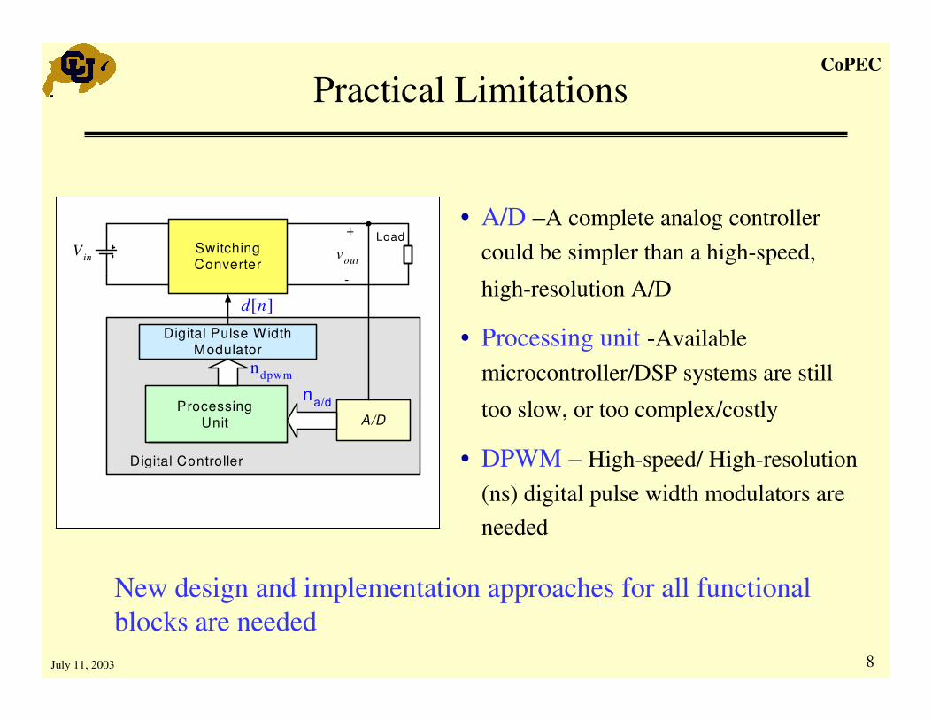
Practical Limitations
• A/D –A complete analog controller could be simpler than a high-speed,
high-resolution A/D
• Processing unit -Available microcontroller/DSP systems are still
too slow, or too complex/costly
• DPWM – High-speed/ High-resolution (ns) digital pulse width modulators are needed
New design and implementation approaches for all functionalblocks are needed
text
LoadVin
A/DProcessing
Unit
Digital Pulse WidthModulator
ndpwm
na/d
SwitchingConverter
vout
+
-
d[n]
Digital Controller

CoPEC
9July 11, 2003
CoPEC Research ProgramPower Electronics and Mixed-Signal IC Design
Hardware-accelerated
computationalunit
Small, fast,scalable A/Dconverters
Programmabledigital
modulators Serial I/O
Standard µC or DSP core and peripherals
Switching power converter
Digital SMPS controller
System interface
Dig
ital s
igna
l tra
nsm
issi
onac
ross
isol
atio
n bo
unda
ry
Pin PoutGate-drive waveforms Voltage/current sensing
New converter configurations tied to more sophisticated control techniques
New SMPS-specific controller building blocks
New controller architectures for wide range of applications
New control algorithms• parameter/state estimation• adaptive control• nonlinear control, etc.Modeling techniques
Converter/controller co-design for significant gains in performance, size and/or cost:• reduced size of passive components• improved efficiency• improved dynamic responses, etc.
CoPEC
10July 11, 2003
Examples of CoPEC Research Results
• Complete 1 MHz digital PWM controller IC– small size, programmable compensator, no discretes
• Standard-cell based A/D converter ICs– small size, fast sampling, scalable with digital technology
• Digitally controlled 3.3 V, 20 A DC power supply– chipset for isolated DC power supplies
• Digital predictive current-mode control– very fast response– applications to PFC and DC-DC converters
• Digitally-controlled power-factor correction rectifiers– order-of-magnitude improvement in dynamic response
CoPEC
11July 11, 2003
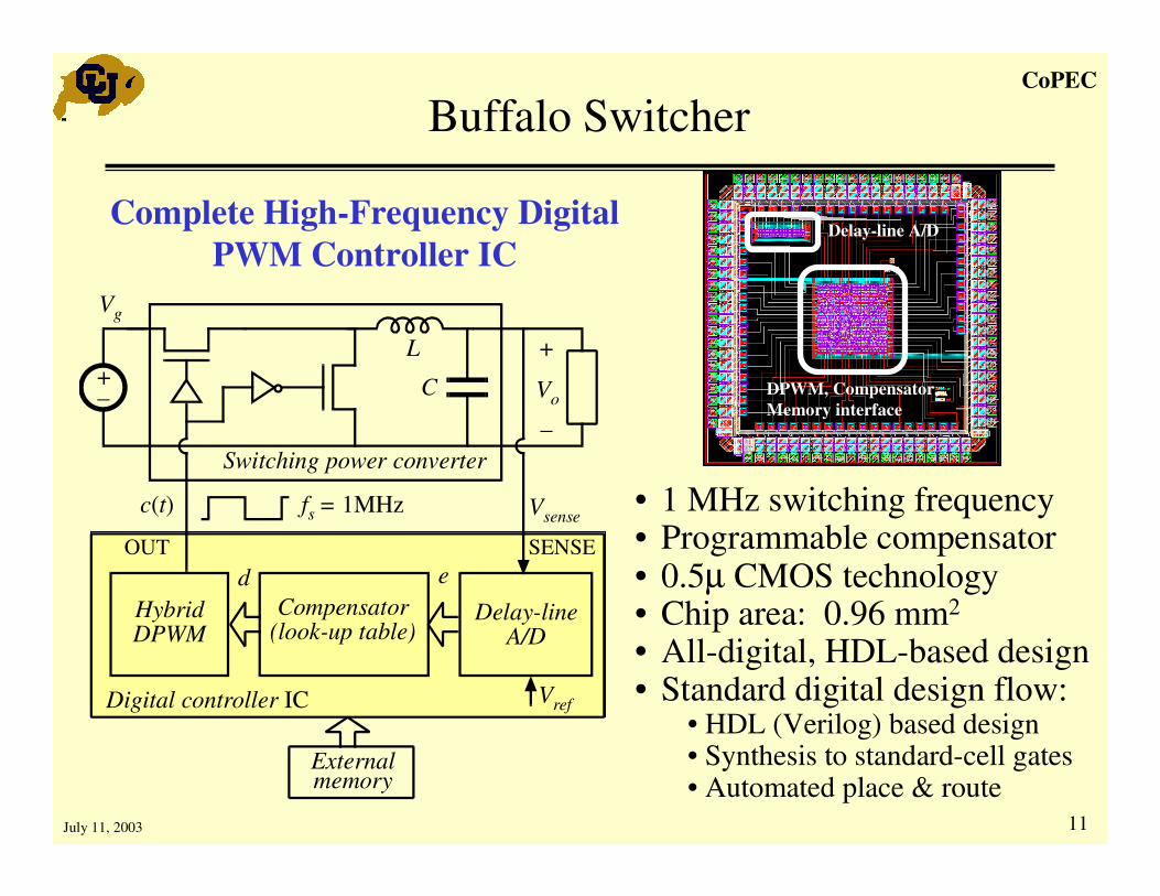
Buffalo Switcher
Externalmemory
HybridDPWM
Delay-lineA/D
Compensator(look-up table)
ed
VrefDigital controller IC
SENSEOUT
Switching power converter
Vg
Vo
c(t)
+–
+
_
fs = 1MHz Vsense
L
C
Delay-line A/D
DPWM, Compensator, Memory interface
• 1 MHz switching frequency• Programmable compensator• 0.5µ CMOS technology• Chip area: 0.96 mm2
• All-digital, HDL-based design• Standard digital design flow:
• HDL (Verilog) based design• Synthesis to standard-cell gates• Automated place & route
Complete High-Frequency Digital PWM Controller IC
CoPEC
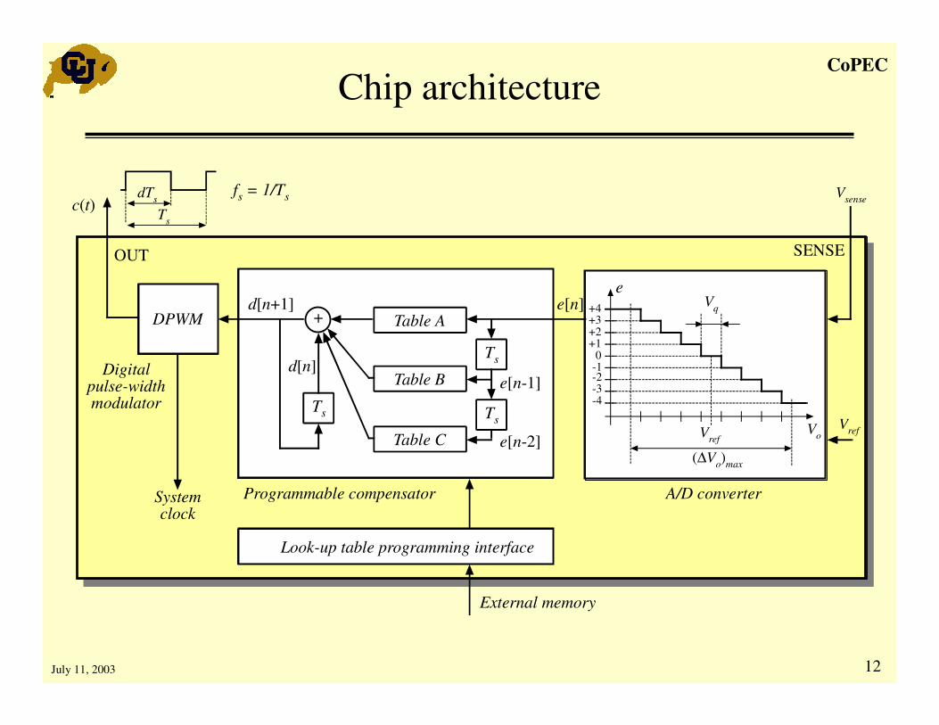
12July 11, 2003
Chip architecture
c(t)
Vo
e
Vref
-2
+10
Vqe[n]
e[n-1]
e[n-2]
d[n]
+d[n+1]
DPWM
Programmable compensator A/D converter
Digitalpulse-widthmodulator Ts Ts
Ts
Vref
Vsense
Ts
dTsfs = 1/Ts
OUT SENSE
-3-4
+2+3+4
-1
(∆Vo)max
Table A
Table B
Table C
Look-up table programming interface
External memory
Systemclock
CoPEC
13July 11, 2003
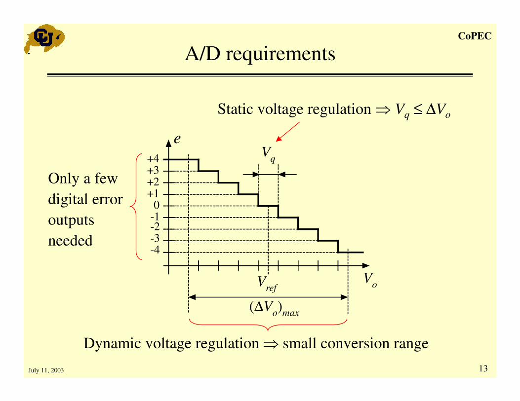
A/D requirements
Static voltage regulation � Vq ≤ ∆Vo
Dynamic voltage regulation � small conversion range
Only a few digital error outputs needed
Vo
e
Vref
-2
+10
Vq
-3-4
+2+3+4
-1
(∆Vo)max
CoPEC
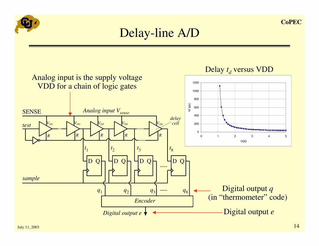
14July 11, 2003
Delay-line A/D
0
200
400
600
800
1000
1200
0 1 2 3 4 5
VDD
td (p
s)
Analog input is the supply voltage VDD for a chain of logic gates
Delay td versus VDD
Digital output q(in “thermometer” code)
Digital output e
D Q
VDD VDD VDD VDDVDD
D Q D Q D Q
Digital output e
sample
test
Analog input Vsensedelaycell
t1 t2 t3 t8
q1 q2 q3 q8
Encoder
R R R R R
SENSE

CoPEC
15July 11, 2003
Delay-line A/D Operation
Start conversion
End conversion
11
111
100
q = {11111100}e = -2
Ts
sample
test
t1
t2
t3
t4
t5
t6
t7
t8
0
td

CoPEC
16July 11, 2003
Delay-line A/D Experimental Results
Vq = 53mV, σ = 3.6mVfs = 1 MHz sampling
Vref Vref +0.1 V Vref +0.2 VVref – 0.1 VVref – 0.2 V
0
+1
+2
+3
+4
–1
–2
–3
–4
Vsense
e
Vq
Error e
Sampled output voltage Vsense
Zero-error bin
Advantages:• Small area/low power• Averaging over
conversion time• All digital
implementationProblem:• Basic configuration is
highly susceptible to process/temperature
• How to implement calibration to a reference voltage?

CoPEC
17July 11, 2003
Strobe-Calibrated Delay-Line A/D
• Delay blocks constructed with standard cells• Matched “strobe delay” added to provide self-
calibrated reference point
delayblock
1
delayblock
2
delayblockN/2
delayblockN-1
delayblock
N
DQ
DQ
DQ
DQ
DQ
Strobe Delay
Vsense
delay input
reset
therm<0> therm<1> therm<N/2> therm<N-1> therm<N>
Vref
strobe
CoPEC
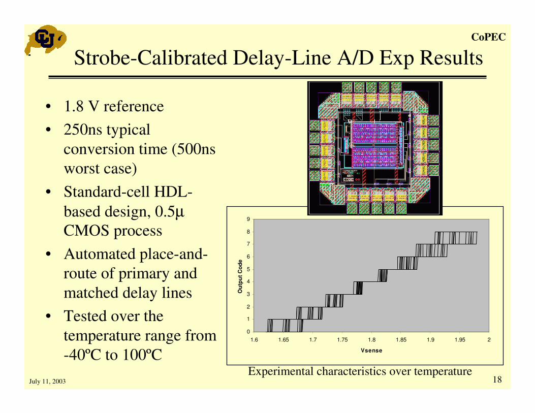
18July 11, 2003
0
1
2
3
4
5
6
7
8
9
1.6 1.65 1.7 1.75 1.8 1.85 1.9 1.95 2
Vsense
Out
put C
ode
Experimental characteristics over temperature
Strobe-Calibrated Delay-Line A/D Exp Results
• 1.8 V reference• 250ns typical
conversion time (500ns worst case)
• Standard-cell HDL-based design, 0.5µCMOS process
• Automated place-and-route of primary and matched delay lines
• Tested over the temperature range from -40ºC to 100ºC
CoPEC
19July 11, 2003
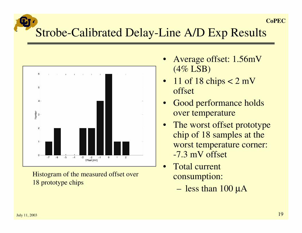
Strobe-Calibrated Delay-Line A/D Exp Results
• Average offset: 1.56mV (4% LSB)
• 11 of 18 chips < 2 mV offset
• Good performance holds over temperature
• The worst offset prototype chip of 18 samples at the worst temperature corner: -7.3 mV offset
• Total current consumption: – less than 100 µA
Histogram of the measured offset over 18 prototype chips

CoPEC
20July 11, 2003
Look-up Table Based Programmable Compensator
Programmable compensator
External memory
e[n]
e[n-1]
e[n-2]
d[n]
+d[n+1]
Ts Ts
Ts
Table A
Table B
Table C
Error fromA/D
Duty-cycleto
DPWM
PID compensator: d[n+1] = d[n] + a e[n] + b e[n-1] + c e[n-1]
Table A Table B Table C
8-bit
•“Zero” steady-state error•Programmable response•Very small area, very low power
CoPEC
21July 11, 2003
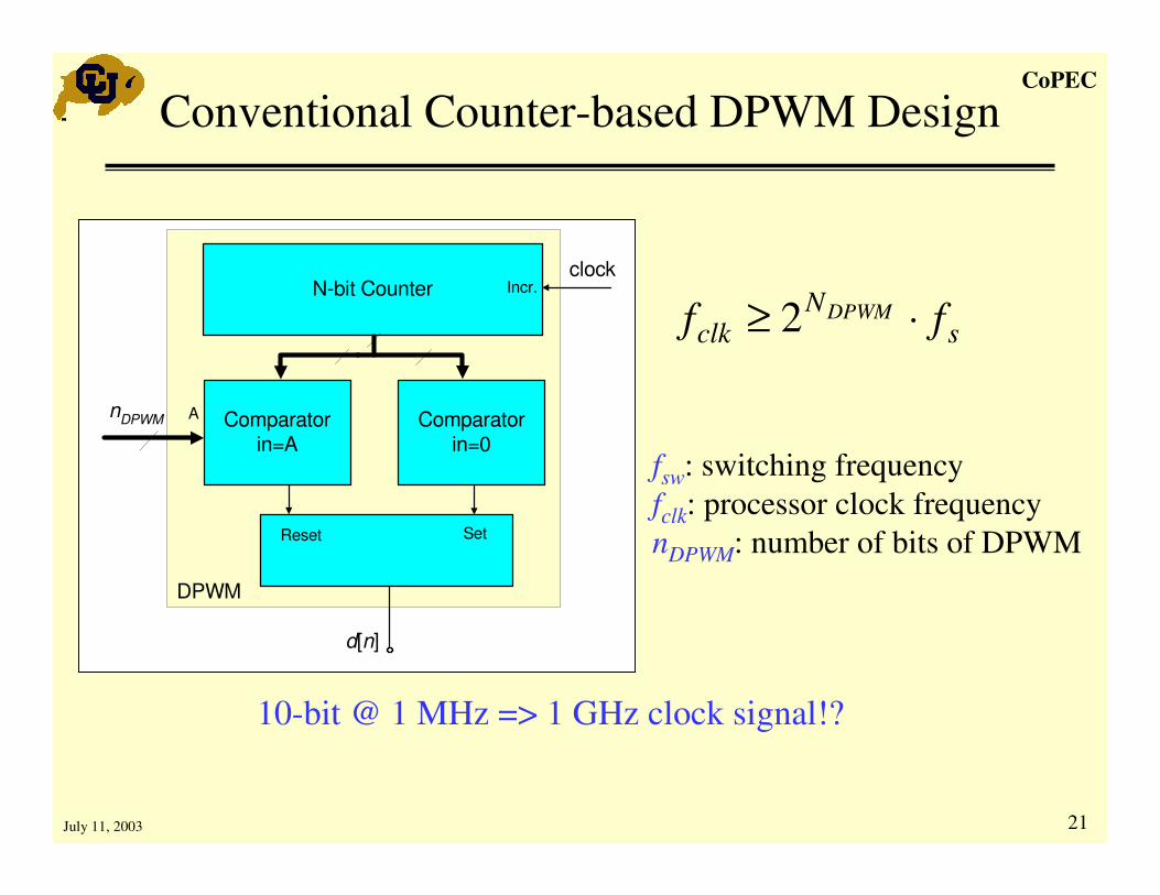
Conventional Counter-based DPWM Design
sN
clk ff DPWM ⋅≥ 2
fsw: switching frequencyfclk: processor clock frequencynDPWM: number of bits of DPWM
10-bit @ 1 MHz => 1 GHz clock signal!?
Comparatorin=A
A Comparatorin=0
N-bit Counterclock
Reset Set
Incr.
DPWM
nDPWM
d[n]

CoPEC
22July 11, 2003
High-Resolution Hybrid DPWM
+VDD 2-bitcounter
+1 out[1:0]
nc-bitcomparator 1
(a ?= b)
a[1:0]
b[1:0]
out(a=b)
d[3:2]
d[1:0] 0 1 2 3
R
S
Qa[1:0]
b[1:0]
out(a=b)
cnt[1:0]
cnt[1:0] OUT
Q0
Reset
Set
D QR
D QR
D QR
D QR
2nd
:1 MUX
d[3:0]input
systemclock
Q1 Q2 Q3
nnc
nd
nc-bitcomparator 2
(a ?= b)
nc
nc
c(t)
Conventional DPWM:fclk = 2n ⋅ fs
Hybrid DPWM:fs ≤ fclk ≤ 2n ⋅ fs
Prototype:n = 8 bitsfs = 1 MHzfclk = 8 MHz
Combines a delay line (ring oscillator) with a counter to reduce the maximum clock speed

CoPEC
23July 11, 2003
DPWM Experimental Results
0 32 64 96 128 160 192 224 2550
10
20
30
40
50
60
70
80
90
100Output duty ratio [%]
DPWM input (decimal)

CoPEC
24July 11, 2003
High-Resolution Hybrid DPWM
Conventional DPWM:fclk = 2n ⋅ fs
n = 8 bitsfs = 1 MHzfclk = 256 MHz
Hybrid DPWM:fs ≤ fclk ≤ 2n ⋅ fs
Buffalo switcher hybrid DPWM prototype:
n = 8 bitsfs = 1 MHzfclk = 8 MHz
Hybrid DPWM combines a delay line (ring oscillator) with a counter to reduce the maximum clock speed
+VDD 2-bitcounter
+1 out[1:0]
nc-bitcomparator 1
(a ?= b)
a[1:0]
b[1:0]
out(a=b)
d[3:2]
d[1:0] 0 1 2 3
R
S
Qa[1:0]
b[1:0]
out(a=b)
cnt[1:0]
cnt[1:0] OUT
Q0
Reset
Set
D QR
D QR
D QR
D QR
2nd
:1 MUX
d[3:0]input
systemclock
Q1 Q2 Q3
nnc
nd
nc-bitcomparator 2
(a ?= b)
nc
nc
c(t)
4-bit hybrid DPWM example

CoPEC
25July 11, 2003
10-bit DPWM With Programmable Frequency
Delay- line/counter combination provides low power consumption, low on-chip area and high resolution at high frequencies
MR
5-bit counter
Input register[9:0]
in [4:0]32:1 Multiplexer
10-bit NOR
in[9:0]
in[9:5]
start
cnt[4:0]
cnt[4]
Vdd
I7
S
R
DPWM
5-bit OR
A B
5-bit comp.
Q
delay
reset reset
Vdd delay
reset
delay
resetI0 I1 I31
delay
fsel[1:0]
Power Onreset-start
reset
A B
DQclr
DQclr
DQclr
A B
DQclr
DQclr
inc.
4:1 Multiplexer
in
fsel[1]fsel[0]
S0
S1
I0 I1 I2 I3
out
delay block
ndpw
Delay line
CoPEC
26July 11, 2003
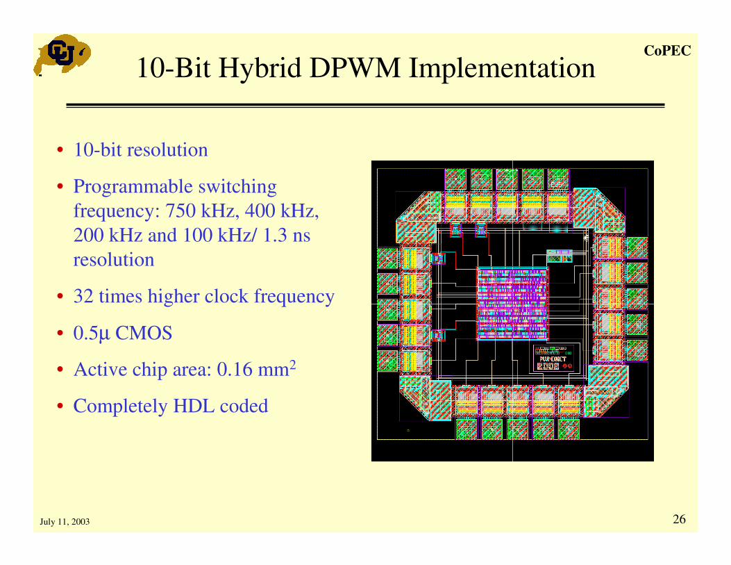
10-Bit Hybrid DPWM Implementation
• 10-bit resolution
• Programmable switching frequency: 750 kHz, 400 kHz, 200 kHz and 100 kHz/ 1.3 ns resolution
• 32 times higher clock frequency
• 0.5µ CMOS
• Active chip area: 0.16 mm2
• Completely HDL coded
CoPEC
27July 11, 2003
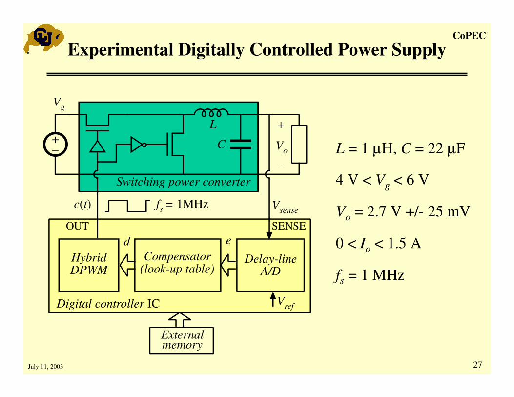
Experimental Digitally Controlled Power Supply
L = 1 µH, C = 22 µF
4 V < Vg < 6 V
Vo = 2.7 V +/- 25 mV
0 < Io < 1.5 A
fs = 1 MHz
Externalmemory
HybridDPWM
Delay-lineA/D
Compensator(look-up table)
ed
VrefDigital controller IC
SENSEOUT
Switching power converter
Vg
Vo
c(t)
+–
+
_
fs = 1MHz Vsense
L
C

CoPEC
28July 11, 2003
Experimental Results
Input voltage
Out
put v
olta
ge e
rror
+10
+20
+30
Vo – Vref [mV]
–10
–20
–30
0
Vg [V]
3.5 4.0 4.5 5.0 5.5 6.0 6.5
+10
+20
+30
–10
–20
–30
0
0.2 0.4 0.6 0.8 1.0 1.2 1.4 1.6 1.8 2.00
Vo – Vref [mV]
Io [A]
Out
put v
olta
ge e
rror
Load current
Static line regulation
Static load regulation
0 A
1 A
Vo(t) [50 mV/div]
Vq
Io(t) [1 A/div]
Load Transient Response

CoPEC
29July 11, 2003
Conclusions
• Complete 1 MHz digital PWM controller IC• New architecture and HDL-based design of the key building
blocks: – Calibrated delay-line A/D– Programmable look-up table compensator– Hybrid DPWM
• Small area, low power, fast response • Design scales with digital technology• Open possibilities for a new generation of controller ICs
(standard parts and ASICs) for power electronics
CoPEC
30July 11, 2003
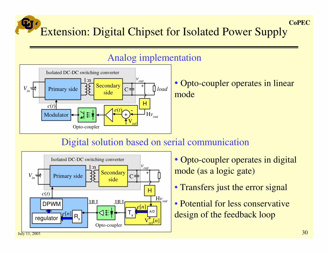
• Opto-coupler operates in linear mode
Digital solution based on serial communication
Primary sideVinSecondary
side C
1:n vout+
Isolated DC-DC switching converter
Modulator Hvout
Opto-coupler
c(t)+ -
Vref
e(t)H
load
Analog implementation
Extension: Digital Chipset for Isolated Power Supply
Primary sideVinSecondary
side C
1:n vout+
Isolated DC-DC switching converter
Hc(t)Hvout
Opto-coupler
A/DTxVref[n]
e[n]
Rx
DPWM
regulatore[n]
• Opto-coupler operates in digital mode (as a logic gate)
• Transfers just the error signal
• Potential for less conservative design of the feedback loop

CoPEC
31July 11, 2003
fsel[1:0]DPWM
Regulator
Primary side IC
d[n]
ndpw
Serialreceiver
e[n]
16 x fsw clk_out
ser_in
oc1
oc2
Serialtransmitter
ser_out
+
Secondary side IC
Vrefclk_ine[n]
Isolated DC-DC: Test System
Tyco HW 100F
• Isolated converter
• 36 V ÷ 72 V to 3.3 V
• up to 20 Amps load
• 400 kHz switching frequency
• Replaced original analog current-mode controller on the board

CoPEC
32July 11, 2003
Experimental Results
load current
output voltage
50% load current
output voltage
25%25%50%
Original analog controller Digital controller IC set

CoPEC
33July 11, 2003
Digital Controller for AC/DC PFC
+
-
ig(t)vin(t)
A/D
+Vref[n]
Load
-
+
A/D
vin[n]
DPWM
u[n]=avu[n-1]+Kv(bvev[n]-cvev[n-1])
A/D
vo[n]
ev[n]
Voltage loop regulator
vo(t)Vin
vo(t)
ig[n]
iref [n]
d[n]
d(t)
vo[n]
Computational UnitComputational Unit
)1()1()1()1(
)( 1)1(1
)1(1
−+−−
+−−
−⋅−−⋅−=
zrzzrz
zH M
M
�=
N
nnx
N 1][
1
comparator
Sampling frequencyselector
e[n]
y[n] s[n]
Vv
iniVT
Lndnd in
refgs
2)]1[(]1[2][ −−−−−−=
Deadbeat Control
Comb Filter
Switching Power Converter
Analog/DigitalAnalog/DigitalInterfaceInterface
Rectified AC line voltage input

CoPEC
34July 11, 2003
PFC Experimental Results (current loop)
Switching frequency: 200KHzTHD: 2.2%
Line frequency: 800Hz
Switching frequency: 100KHzTHD: 2.4%
Dead-beat digital current mode control: near-perfect PFC even in demanding next-generation avionics applications (AC system with the line frequency up to 800 Hz)

CoPEC
35July 11, 2003
PFC Experimental Results (voltage loop)
With STCF
Conventional voltage loop
Output voltage
Load current
Line current
High-bandwidth loop with and without a notch filter
With comb
Without combTHD > 20%
THD = 4.3%
Output voltage
Load current
Line current

CoPEC
36July 11, 2003
Other CoPEC Research Projects (2003)
• Advanced digital control of DC-DC converters� High-performance predictive digital current-mode control for DC-DC converters
(TI)
• Power management for low-power electronics� Digital DC-DC switcher for battery-powered systems (NSC)� Adaptive DC-DC converters for RF power amplifiers (DARPA)� Adaptive DC-DC converters and power management architecture for base-band
µP/DSP (NSF, NSC)� Energy harvesting for wireless sensors and Implantable sensors for neuronal
recording (Coleman Institute)
• Microprocessor power supplies� Multi-phase digital controller for microprocessor power supplies (Artesyn)
• Off-line switching power supplies� Modular mixed-signal control for electronic ballasts (GE)� Digital controllers for solar/utility power system (Philips)� Digitally controlled matrix converters for wind power system (NREL)

CoPEC
37July 11, 2003
CoPEC Educational Program Objectives
• Strong undergraduate and graduate programs in power electronics and mixed-signal IC design
• Internship and job opportunities for students• Continuing education
– Courses available through CATECS– Certificate program in power electronics
• Technology transfer to CoPEC sponsors– Jointly defined and directed projects– Access to CoPEC IP

CoPEC
38July 11, 2003
Growth of Program: Enrollment
������������ ������ ��������
�
��
��
��
��
��
��
��� ��� ��� ��� ��� ���
�������
�� ������
��
��
������������� ��� ������ ����
�
�
��
��
��
��
��
��
��
��
������� ������� �������
�������
�� ������
������
��
��
Our visibility is increasing, and we are attracting more students to the power electronics and micro-electronics areas
Enrollment for Analog IC Design, Spring 2002: 31, Spring 2003: 66Enrollment for Mixed-Signal IC Design, Fall 2002: 15

CoPEC
39July 11, 2003
Growth of Program: Graduate Students
With increased visibility and availability of projects, we are able to attract better students into our program
Power Electronics Program
0
2
4
6
8
10
12
14
16
2000 2001 2002 2003
Year
Num
ber o
f gra
duat
e st
uden
ts
other
TA
other RA
CoPEC RA

CoPEC
40July 11, 2003
Mixed-Signal IC Design FlowSystem/Application Specification
IC Specification
IC Functional DescriptionAnalog/Digital Distribution
Functional AnalogCircuit & Verilog-A
Functional DigitalVerilog/VHDL
Complete Analog Synthesis
Complete Design
LayoutCustom, Place & Route, DRC
Tape-Out
VerificationLVS, Extraction
Mixed-SignalSimulation Digital
SimAnalog
Sim
4228/5008: Analog IC• Spring 2003• Analog portion only
5007: Mixed-Signal IC• Fall 2003• Full System• Emphasis on mixed blocks

CoPEC
41July 11, 2003
Analog IC Course Outline
• Week 1: Review circuits I-II• Text Ch. 1, Appendix A & C; Supplementary notes
• Week 2: Review CMOS technology and device models• Text Ch. 2-3
• Weeks 3-4: Analog CMOS sub-circuits• Text Ch. 4
• Weeks 5-7: CMOS amplifiers• Text Ch. 5
• Weeks 8-10: CMOS operational amplifiers• Text Ch. 6
• Weeks 11-13: High-performance CMOS op-amps• Text Ch. 7
• Weeks 14-15: Comparators and select advanced topics• Text Ch. 8, Supplementary notes
Text used: Allen/Holberg, Gray/Meyer, Johns/Martin
CoPEC
42July 11, 2003
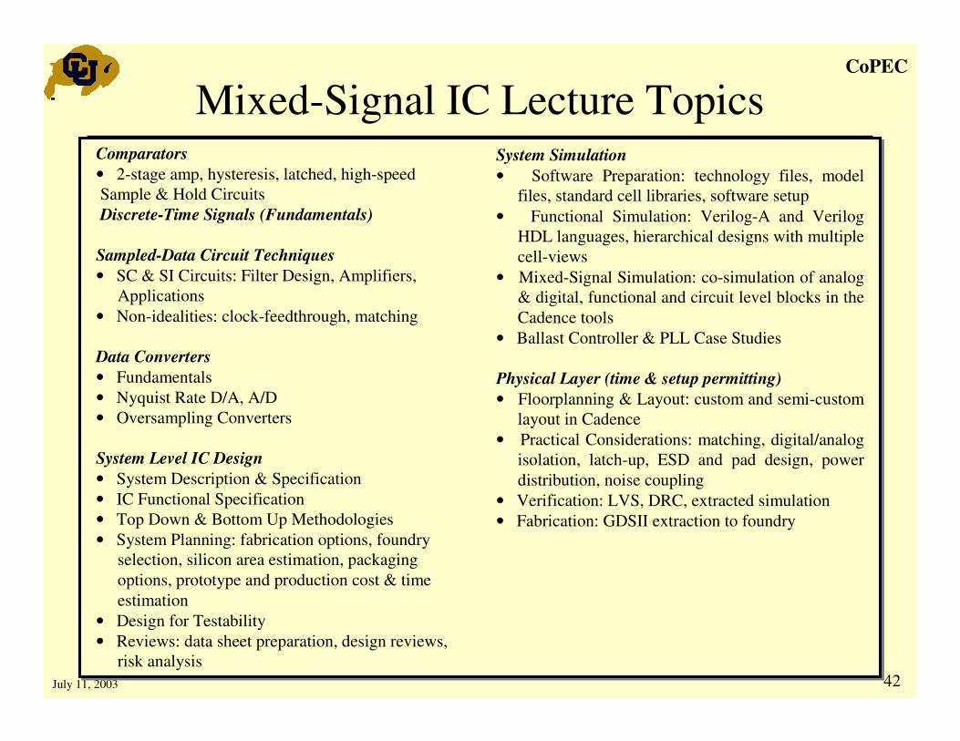
Mixed-Signal IC Lecture TopicsComparators• 2-stage amp, hysteresis, latched, high-speedSample & Hold CircuitsDiscrete-Time Signals (Fundamentals)
Sampled-Data Circuit Techniques• SC & SI Circuits: Filter Design, Amplifiers,
Applications• Non-idealities: clock-feedthrough, matching
Data Converters• Fundamentals• Nyquist Rate D/A, A/D• Oversampling Converters
System Level IC Design• System Description & Specification• IC Functional Specification• Top Down & Bottom Up Methodologies• System Planning: fabrication options, foundry
selection, silicon area estimation, packaging options, prototype and production cost & time estimation
• Design for Testability• Reviews: data sheet preparation, design reviews,
risk analysis
System Simulation• Software Preparation: technology files, model
files, standard cell libraries, software setup• Functional Simulation: Verilog-A and Verilog
HDL languages, hierarchical designs with multiple cell-views
• Mixed-Signal Simulation: co-simulation of analog & digital, functional and circuit level blocks in the Cadence tools
• Ballast Controller & PLL Case Studies
Physical Layer (time & setup permitting)• Floorplanning & Layout: custom and semi-custom
layout in Cadence• Practical Considerations: matching, digital/analog
isolation, latch-up, ESD and pad design, power distribution, noise coupling
• Verification: LVS, DRC, extracted simulation• Fabrication: GDSII extraction to foundry

CoPEC
43July 11, 2003
Mixed-Signal IC Final Project
• Select a mixed-signal project that targets a specific application• Work in teams of 1 to 4• Deliverables include:
• Proposal: Create a final project website with an overview of the target application, preliminary IC specifications, and a functional description of the digital & analog IC blocks – Due Oct 17
• Functional Design Review: In-class presentation on your results to date, which must include system level simulations verifying yourfunctional blocks in the application environment. Simulations must include at least one block of each: Verilog-A, Verilog or VHDL, and a circuit level block. Include your presentation and simulation files on your project website. Reviews Scheduled Nov 5-14
• Final Design Review: Final in-class presentation on your project. The complete “front-end” design of the projects must be complete, ready for transition to a layout engineer. Time permitting, various phases of layout and verification may be required as well.
Local Industry Involvement (?)• Suggest relevant project/research topics• Be involved with design and/or final
reviews• Fund fabrication of best designs � hold
competition?
Local Industry Involvement (?)• Suggest relevant project/research topics• Be involved with design and/or final
reviews• Fund fabrication of best designs � hold
competition?