customer - adafruit industries · kd----(2) displaymonitor oppositeanglelinesize ......
TRANSCRIPT
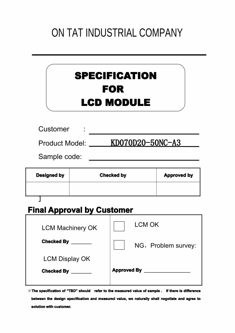
SPECIFICATIONSPECIFICATIONSPECIFICATIONSPECIFICATIONFORFORFORFOR
LCDLCDLCDLCD MODULEMODULEMODULEMODULE
Customer :
]
Product Model: KD070D20-50NC-A3
DesignedDesignedDesignedDesigned bybybyby CheckedCheckedCheckedChecked bybybyby ApprovedApprovedApprovedApproved bybybyby
FinalFinalFinalFinal ApprovalApprovalApprovalApproval bybybyby CustomerCustomerCustomerCustomer
LCM Machinery OK
CheckedCheckedCheckedChecked ByByByBy
LCM Display OK
CheckedCheckedCheckedChecked ByByByBy
LCM OK
NG,Problem survey:
ApprovedApprovedApprovedApproved ByByByBy
※TheTheTheThe specificationspecificationspecificationspecification ofofofof ““““TBDTBDTBDTBD”””” shouldshouldshouldshould referreferreferrefer totototo thethethethe measuredmeasuredmeasuredmeasured valuevaluevaluevalue ofofofof samplesamplesamplesample .... IfIfIfIf theretheretherethere isisisis differencedifferencedifferencedifference
betweenbetweenbetweenbetween thethethethe designdesigndesigndesign specificationspecificationspecificationspecification andandandand measuredmeasuredmeasuredmeasured value,value,value,value, wewewewe naturallynaturallynaturallynaturally shallshallshallshall negotiatenegotiatenegotiatenegotiate andandandand agreeagreeagreeagree totototo
solutionsolutionsolutionsolution withwithwithwith customer.customer.customer.customer.
Sample code:
ON TAT INDUSTRIAL COMPANY
KD0KD0KD0KD077770D0D0D0D22220000-50N-50N-50N-50NCCCC----A3A3A3A3
©All Rights Reserved 2/26 REV A
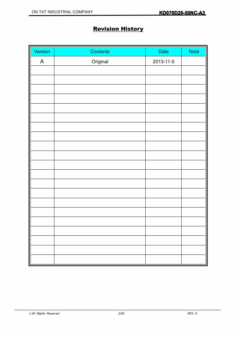
Revision History
Version Contents Date Note
A Original 2013-11-5
ON TAT INDUSTRIAL COMPANY
KD0KD0KD0KD077770D0D0D0D22220000-50N-50N-50N-50NCCCC----A3A3A3A3
©All Rights Reserved 3/26 REV A
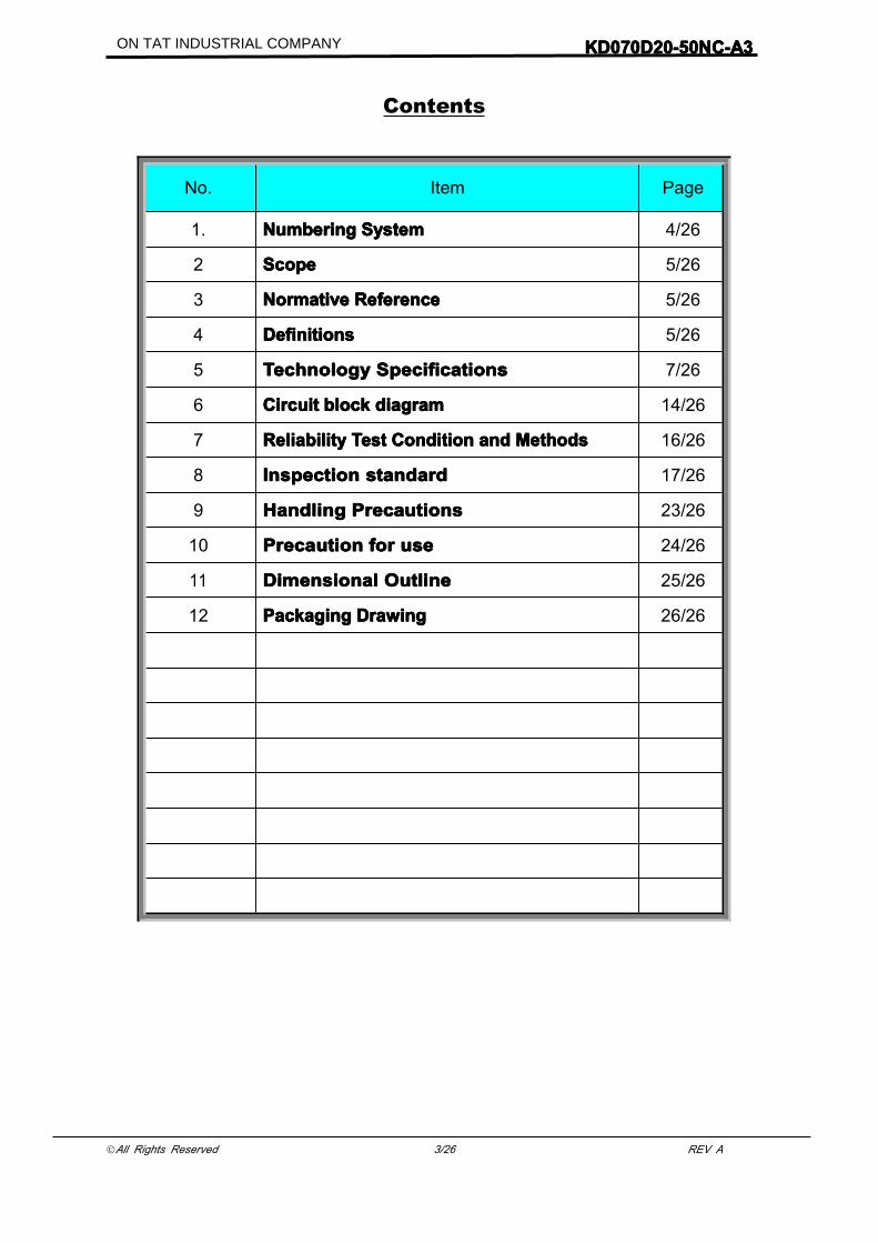
Contents
No. Item Page
1. NumberingNumberingNumberingNumbering SystemSystemSystemSystem 4/26
2 ScopeScopeScopeScope 5/26
3 NormativeNormativeNormativeNormative ReferenceReferenceReferenceReference 5/26
4 DDDDefinitionsefinitionsefinitionsefinitions 5/26
5 TechnologyTechnologyTechnologyTechnology SpecificationsSpecificationsSpecificationsSpecifications 7/26
6 CircuitCircuitCircuitCircuit blockblockblockblock diagramdiagramdiagramdiagram 14/26
7 ReliabilityReliabilityReliabilityReliability TestTestTestTest ConditionConditionConditionCondition andandandand MethodsMethodsMethodsMethods 16/26
8 InspectionInspectionInspectionInspection standardstandardstandardstandard 17/26
9 HandlingHandlingHandlingHandling PrecautionsPrecautionsPrecautionsPrecautions 23/26
10 PrecaPrecaPrecaPrecautionutionutionution forforforfor useuseuseuse 24/26
11 DimensionalDimensionalDimensionalDimensional OutlineOutlineOutlineOutline 25/26
12 PackagingPackagingPackagingPackaging DrawingDrawingDrawingDrawing 26/26
ON TAT INDUSTRIAL COMPANY
KD0KD0KD0KD077770D0D0D0D22220000-50N-50N-50N-50NCCCC----A3A3A3A3
©All Rights Reserved 4/26 REV A
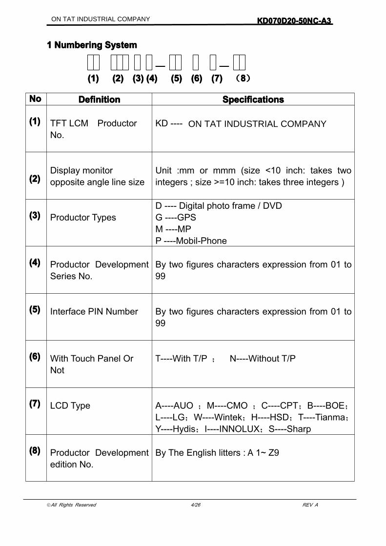
1111 NumberingNumberingNumberingNumbering SystemSystemSystemSystem
— —
(1)(1)(1)(1) (2)(2)(2)(2) (3)(3)(3)(3) (4)(4)(4)(4) (5)(5)(5)(5) (6)(6)(6)(6) (7)(7)(7)(7) (8888)
NoNoNoNo DefinitionDefinitionDefinitionDefinition SpecificationsSpecificationsSpecificationsSpecifications
(1)(1)(1)(1) TFT LCM ProductorNo.
KD ----
(2)(2)(2)(2)Display monitoropposite angle line size
Unit :mm or mmm (size <10 inch: takes twointegers ; size >=10 inch: takes three integers )
(3)(3)(3)(3) Productor TypesD ---- Digital photo frame / DVDG ----GPSM ----MPP ----Mobil-Phone
(4)(4)(4)(4) Productor DevelopmentSeries No.
By two figures characters expression from 01 to99
((((5555)))) Interface PIN Number By two figures characters expression from 01 to99
(6)(6)(6)(6) With Touch Panel OrNot
T----With T/P ; N----Without T/P
(7)(7)(7)(7) LCD Type A----AUO ;M----CMO ;C----CPT;B----BOE;L----LG;W----Wintek;H----HSD;T----Tianma;Y----Hydis;I----INNOLUX;S----Sharp
(8)(8)(8)(8) Productor Developmentedition No.
By The English litters : A 1~ Z9
ON TAT INDUSTRIAL COMPANY
ON TAT INDUSTRIAL COMPANY

KD0KD0KD0KD077770D0D0D0D22220000-50N-50N-50N-50NCCCC----A3A3A3A3
©All Rights Reserved 5/26 REV A
2222 ScopeScopeScopeScope
This specification applies to the TFT LCD module which is designed andmanufactured by LCM Factory of
3333 NormativeNormativeNormativeNormative ReferenceReferenceReferenceReferenceGB/T4619-1996 《 Liquid Crystal Display Test Method》GB/T2424 《Basic environmental Testing Procedures for Electric and Electronic
Products.》GB/T2423 《Basic Testing Procedures for Electric and Electronic Products》IEC61747-1 《SIXTH PARTGB2828`2829-87《National Standard of PRC》
4444 DDDDefinitionsefinitionsefinitionsefinitions
4444.1.1.1.1 DefinitionsDefinitionsDefinitionsDefinitions ooooffff VopVopVopVopThe definitions of threshold voltage Vth1, Vth2 the following typical waveforms
are applied on liquid crystal by the method of equalized voltage for each duty andbias.
【 selected waveform 】 【 non-selected waveform 】
① Vth1: The voltage which the brightness of segment indicates 50% ofsaturated value on the conditions of selected waveform
(ff=80Hz, Φ=10°θ=270° at 25℃)
② Vth2: The voltage which the brightness of segment indicates 50% ofsaturated value on the conditions of non-selected waveform
(ff=80Hz, Φ=10°θ=270° at 25℃)
③ Vop: (Vth1(50%)+Vth2(50%))/2 (ff=80Hz, Φ=10°θ=270° at 25℃)
4444.2.2.2.2 DDDDefinitionefinitionefinitionefinition ofofofof RRRResponseesponseesponseesponse TTTTimeimeimeime TTTTr,r,r,r, TTTTdddd①Tr: The time required which the brightness of segment
becomes 10% from 100% when waveform is switched toselected one from non-selected one. (ff=80Hz, Φ=10 °
θ=270° at 25℃)
②Td: The time required which the brightness of segment
ON TAT INDUSTRIAL COMPANY
ON TAT INDUSTRIAL COMPANY

KD0KD0KD0KD077770D0D0D0D22220000-50N-50N-50N-50NCCCC----A3A3A3A3
©All Rights Reserved 6/26 REV A
becomes 90% from 10% when waveform is switched toselected one from selected one. (ff=80Hz, Φ=10°θ=270° at25℃)
4444.3.3.3.3 DefinitionDefinitionDefinitionDefinition ooooffff ContrastContrastContrastContrast RatioRatioRatioRatio CrCrCrCrCr=A/B
1 A: Segments brightness in case of non-selected waveform2 B: Segments brightness in case of selected waveform
4444.4.4.4.4 DefinitionDefinitionDefinitionDefinition ofofofof AngleAngleAngleAngle andandandand ViewingViewingViewingViewing RangeRangeRangeRange
Angular Graph: Constrast Ratio
Such as:Viewing Angle Range:
80(Cr>2) Horizontal70(Cr>2) Vertical
ON TAT INDUSTRIAL COMPANY

KD0KD0KD0KD077770D0D0D0D22220000-50N-50N-50N-50NCCCC----A3A3A3A3
©All Rights Reserved 7/26 REV A
5555 TechnologyTechnologyTechnologyTechnology SpecificationsSpecificationsSpecificationsSpecifications
5555.1.1.1.1 FeatureFeatureFeatureFeatureThis single-display module is suitable for use in Multimedia Player products.
The LCD adopts one backlight with High brightness 15-lamps white LED.1) Construction: 7〞а-Si color TFT-LCD ,White LED backlight and FPC.
2) LCD:2.1 Amorphous-TFT 7-inch display, transmissive, normally white type.
2.2 1024(RGB)×600 dots Matrix.
2.3 Narrow-contact ledge technique.
3) RGB interface.4) Video signal interface: Parallel RGB.
5.5.5.5.2222 MMMMechanicalechanicalechanicalechanical SpecificationsSpecificationsSpecificationsSpecificationsItem Specifications Unit
Dimensional outline 164.7(W) ×99.8(H) ×2.8(D) mmActive area 154.2144(W) × 85.92(H) mmPixel size 50.2(W) ×RGB×143.2(H) umResolution 1024(RGB) ×600 pixel
Luminance 200(TYP) cd/m2
5.35.35.35.3 AbsoluteAbsoluteAbsoluteAbsolute Max.Max.Max.Max. RatingRatingRatingRating
Item Symbol Values Unit RemarkMin. Max
Power voltage
DVDD -0.3 4.0 VAVDD -0.3 13.5 VVGH -0.3 20 VVGL -20 0.3 V
Operation temperature TOP -10 60 ℃
Storage temperature TST -20 70 ℃
Note: The absolute maximum rating values of this product not allowed to be exceededat any times. Should be module be used with any of absolute maximum ratingsexceeded. The characteristics of the module may not be recovered, or in an extremecase, the module may be permanently destroyed.
ON TAT INDUSTRIAL COMPANY

KD0KD0KD0KD077770D0D0D0D22220000-50N-50N-50N-50NCCCC----A3A3A3A3
©All Rights Reserved 8/26 REV A
5555....4444 EEEElectricallectricallectricallectrical CCCCharacteristicsharacteristicsharacteristicsharacteristicsNote 1
Item Symbol Values Unit RemarkMin. Typ Max
Power voltage
DVDD 3.0 3.3 3.6 V Note 2AVDD 9.4 9.6 9.8 VVGH 17.5 18 18.5 VVGL -6.5 -6 -5.5 V
Input signal voltage VCOM 3.2 3.4 3.6 VInput logic high voltage VIH 0.7DVDD - DVDD V Note 3Input logic low voltage VIL 0 - 0.3DVDD V
Note 1:Be sure to apply DVDD and VGL to the LCD first, and then apply VGH .Note 2: DVDD setting should match the signals output voltage(refer to Note 3) of
Customer’s system board.Note 3: DCLK,HS,VS,RESET,U/D,L/R,DE,R0-R7,G0-G7, G0-G7,MODE,DITHB.
5.55.55.55.5 OOOOpticalpticalpticalptical specificationsspecificationsspecificationsspecifications
Item Symbol ConditionValues
Unit RemarkMin. Typ. Max.
Viewingangle(CR≥ 10)
θLΦ=180°(9o’clock) 70 80 -
degree Note 1θR Φ=0°(3 o’clock) 70 80 -
θTΦ=90°(12o’clock) 60 70 -
θBΦ=270°(6o’clock) 50 60 -
Responsetime
TON
Normalθ=Φ=0°
- 10 20 msec Note 3
TOFF - 15 30 msec Note 3Contrastratio CR 350 400 - - Note 4
Colorchromaticity
WX 0.263 0.313 0.363 - Note 2Note 5Note 6WY 0.279 0.329 0.379 -
Luminance L 180 200 - cd/m2 Note 6
Luminanceuniformity YU 70 75 - % Note 6,7
Test Conditions:1. DVDD=3.3V, ILED=100mA, the ambient temperature is 25℃.2. The test systems refer to Note 2.
ON TAT INDUSTRIAL COMPANY

KD0KD0KD0KD077770D0D0D0D22220000-50N-50N-50N-50NCCCC----A3A3A3A3
©All Rights Reserved 9/26 REV A
Note 1: Definition of viewing angle range
Note 2: Definition of optical measurement system.The optical characteristics should be measured in dark room. After 30minutes operation, the optical properties are measured at the center point ofthe LCD screen. (Viewing angle is measured by ELDIM-EZcontrast/Height :1.2mm ,Response time is measured by Photo detectorTOPCON BM-7, other items are measured by BM-5A/Field of view: 1° /Height: 500mm.)
NormalNormalNormalNormal linelinelinelineθθθθ====ΦΦΦΦ=0=0=0=0°°°°
ΦΦΦΦ====99990000°°°°12121212 oooo’’’’clockclockclockclock directiondirectiondirectiondirection
ΦΦΦΦ====272727270000°°°°6666 oooo’’’’clockclockclockclock directiondirectiondirectiondirection
ΦΦΦΦ=0=0=0=0°°°°ΦΦΦΦ=180=180=180=180°°°°Active Area
θθθθLLLL θθθθTTTTθθθθBBBBθθθθRRRR
PhotoPhotoPhotoPhoto detectordetectordetectordetector
ΦΦΦΦ=90=90=90=90°°°°12121212 oooo’’’’clockclockclockclock directiondirectiondirectiondirection
ΦΦΦΦ=270=270=270=270°°°°6666 oooo’’’’clockclockclockclock directiondirectiondirectiondirection
ΦΦΦΦ=0=0=0=0°°°°ΦΦΦΦ=180=180=180=180°°°°Active Area
500mm500mm500mm500mm
LCM
LCM
NormalNormalNormalNormal linelinelinelineθθθθ====ΦΦΦΦ=0=0=0=0°°°°
ON TAT INDUSTRIAL COMPANY

KD0KD0KD0KD077770D0D0D0D22220000-50N-50N-50N-50NCCCC----A3A3A3A3
©All Rights Reserved 10/26 REV A
Note 3: Definition of Response timeThe response time is defined as the LCD optical switching time intervalbetween “White” state and “Black” state. Rise time (TON) is the time betweenphoto detector output intensity changed from 90% to 10%. And fall time(TOFF) is the time between photo detector output intensity changed from10% to 90%.
100%100%100%100%90%90%90%90%
10%10%10%10%0%0%0%0%
Photo
Photo
Photo
Photodetector
detector
detector
detector
output
output
output
output
(Relative
(Relative
(Relative
(Relativevalue)
value)
value)
value)
TTTTONONONON TTTTOFFOFFOFFOFF
WhiteWhiteWhiteWhite (TFT(TFT(TFT(TFT OFF)OFF)OFF)OFF) BlackBlackBlackBlack (TFT(TFT(TFT(TFT ON)ON)ON)ON) WhiteWhiteWhiteWhite (TFT(TFT(TFT(TFT OFF)OFF)OFF)OFF)
Note 4: Definition of contrast ratio
state Black"" the on LCD whenmeasured Luminancestate White"" the on LCD whenmeasured Luminance
(CR) ratio Contrast =
Note 5: Definition of color chromaticity (CIE1931)Color coordinates measured at center point of LCD.
Note 6: All input terminals LCD panel must be ground while measuring the centerarea of the panel. The LED driving condition is ILED=100mA.
Note 7: Definition of Luminance UniformityActive area is divided into 9 measuring areas. Every measuring point isplaced at the center of each measuring area.
max
min
BB(Yu)Uniformity Luminance =
L-------Active area length W----- Active area widthL
L/6 L/3 L/3
W/6
W/3
W/3
W
Bmax: The measured maximum luminance of all measurement position.Bmin: The measured minimum luminance of all measurement position.
ON TAT INDUSTRIAL COMPANY
KD0KD0KD0KD077770D0D0D0D22220000-50N-50N-50N-50NCCCC----A3A3A3A3
©All Rights Reserved 11/26 REV A
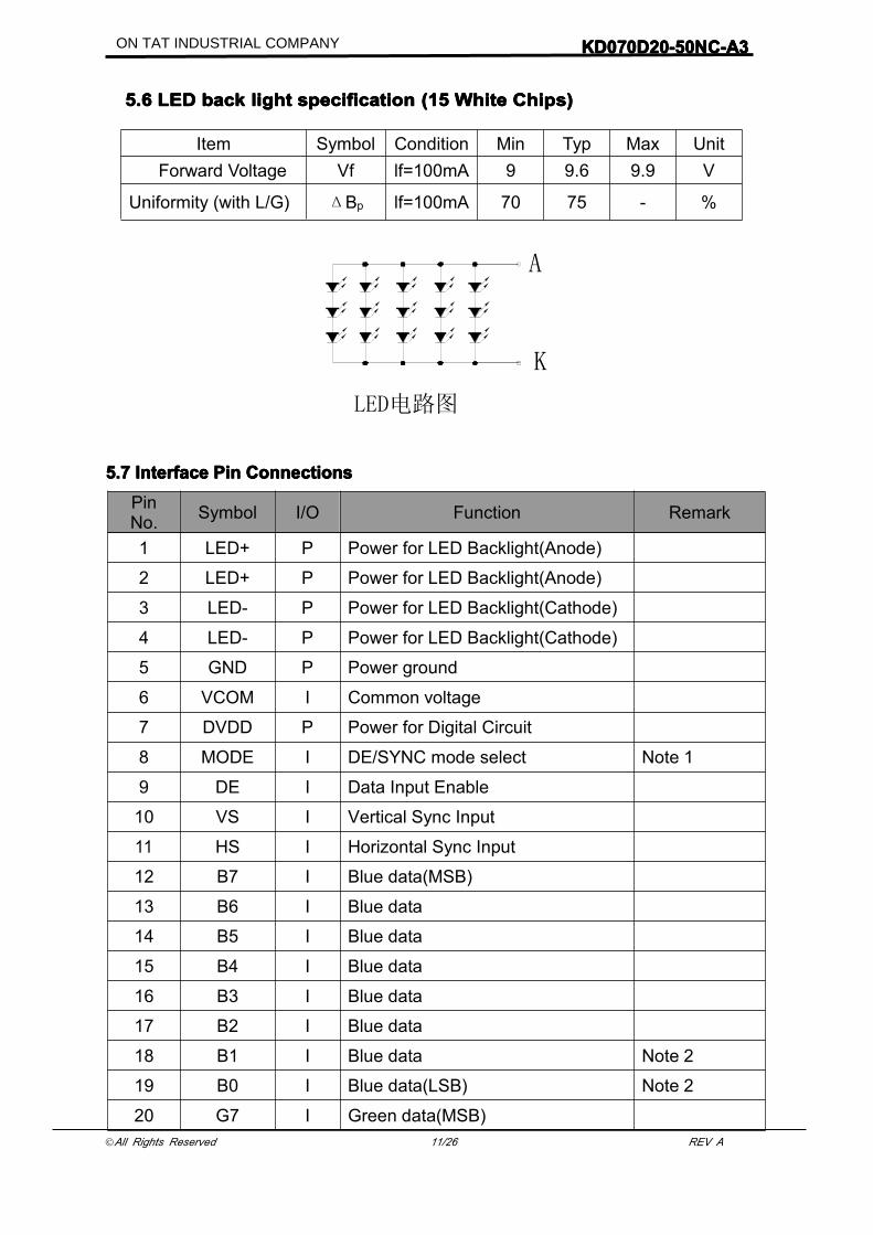
5555....6666 LEDLEDLEDLED backbackbackback lightlightlightlight specificationspecificationspecificationspecification ((((15151515 WhiteWhiteWhiteWhite ChipChipChipChipssss))))
Item Symbol Condition Min Typ Max UnitForward Voltage Vf lf=100mA 9 9.6 9.9 V
Uniformity (with L/G) ΔBp lf=100mA 70 75 - %
LED电路图
A
K
5555.7.7.7.7 InterfaceInterfaceInterfaceInterface PinPinPinPin ConnectionsConnectionsConnectionsConnectionsPinNo. Symbol I/O Function Remark
1 LED+ P Power for LED Backlight(Anode)
2 LED+ P Power for LED Backlight(Anode)
3 LED- P Power for LED Backlight(Cathode)
4 LED- P Power for LED Backlight(Cathode)
5 GND P Power ground
6 VCOM I Common voltage
7 DVDD P Power for Digital Circuit
8 MODE I DE/SYNC mode select Note 1
9 DE I Data Input Enable
10 VS I Vertical Sync Input
11 HS I Horizontal Sync Input
12 B7 I Blue data(MSB)
13 B6 I Blue data
14 B5 I Blue data
15 B4 I Blue data
16 B3 I Blue data
17 B2 I Blue data
18 B1 I Blue data Note 2
19 B0 I Blue data(LSB) Note 2
20 G7 I Green data(MSB)
ON TAT INDUSTRIAL COMPANY

KD0KD0KD0KD077770D0D0D0D22220000-50N-50N-50N-50NCCCC----A3A3A3A3
©All Rights Reserved 12/26 REV A
21 G6 I Green data
22 G5 I Green data
23 G4 I Green data
24 G3 I Green data
25 G2 I Green data
26 G1 I Green data Note 2
27 G0 I Green data(LSB) Note 2
28 R7 I Red data(MSB)
29 R6 I Red data
30 R5 I Red data
31 R4 I Red data
32 R3 I Red data
33 R2 I Red data
34 R1 I Red data Note 2
35 R0 I Red data(LSB) Note 2
36 GND P Power Ground
37 DCLK I Sample clock Note 3
38 GND P Power Ground
39 L/R I Left / right selection Note 4,5
40 U/D I Up/down selection Note 4,5
41 VGH P Gate ON Voltage
42 VGL P Gate OFF Voltage
43 AVDD P Power for Analog Circuit
44 RESET I Global reset pin. Note 6
45 NC - No connection
46 VCOM I Common Voltage
47 DITHB I Dithering function Note 7
48 GND P Power Ground
49 NC - No connection
50 NC - No connectionI: input, O: output, P: Power
Note 1: DE/SYNC mode select. Normally pull high.When select DE mode, MODE=”1”, VS and HS must pull high.When select SYNC mode, MODE=”0”, DE must be grounded.
Note 2: When input 18 bits RGB data, the two low bits of R,G and B data must begrounded.
ON TAT INDUSTRIAL COMPANY

KD0KD0KD0KD077770D0D0D0D22220000-50N-50N-50N-50NCCCC----A3A3A3A3
©All Rights Reserved 13/26 REV A
Note 3: Data shall be latched at the falling edge of DCLK.Note 4: Selection of scanning mode
Setting of scan control inputScanning direction
U/D L/RGND DVDD Up to down, left to right
DVDD GND Down to up, right to leftGND GND Up to down, right to left
DVDD DVDD Down to up, left to right
Note 5: Definition of scanning direction.Refer to the figure as below:
RightLeft
Down
Up
Note 6: Global reset pin. Active low to enter reset state. Suggest to connect withan RC reset circuit for stability. Normally pull high.
Note 7: Dithering function enable control, normally pull high.When DITHB=”0”,Disable internal dithering function,When DITHB=”1”,Enable internal dithering function,
ON TAT INDUSTRIAL COMPANY

KD0KD0KD0KD077770D0D0D0D22220000-50N-50N-50N-50NCCCC----A3A3A3A3
©All Rights Reserved 14/26 REV A
6666 SignalSignalSignalSignal timingtimingtimingtiming diagramdiagramdiagramdiagram6.26.26.26.2 SignalSignalSignalSignal TTTTimingimingimingiming DDDDiagramiagramiagramiagram6.2.16.2.16.2.16.2.1 PowerPowerPowerPower ON/OFFON/OFFON/OFFON/OFF SequenceSequenceSequenceSequencea Power on
b Power off
ON TAT INDUSTRIAL COMPANY

KD0KD0KD0KD077770D0D0D0D22220000-50N-50N-50N-50NCCCC----A3A3A3A3
©All Rights Reserved 15/26 REV A
6.2.26.2.26.2.26.2.2 DataDataDataData inputinputinputinput formatformatformatformat
6.2.36.2.36.2.36.2.3 TimingTimingTimingTiming DiagramDiagramDiagramDiagram
Item Symbol
ValuesUnit Remark
Min Typ Max
Horizontal Display Area thd - 1024 - DCLK
DCLK frequency fck 40.8 51.2 67.2 MHz
One horizontal line th 1114 1344 1400 DCLK
HS pulse width thpw 1 - 140 DCLK
HS Blanking thb 90 320 376 DCLK
HS Front Porch thfp 16 160 216 DCLK
Item SymbolValues
Unit RemarkMin Typ Max
Vertiacl dispaly Area tvd - 600 - TH
VS period time tv 610 635 800 TH
VS pulse width tvpw 1 - 20 TH
VS Blanking tvb 10 35 200 TH
VS Front Porch tvfp 1 12 127 TH
ON TAT INDUSTRIAL COMPANY

KD0KD0KD0KD077770D0D0D0D22220000-50N-50N-50N-50NCCCC----A3A3A3A3
©All Rights Reserved 16/26 REV A
7777 ReliabilityReliabilityReliabilityReliability TestTestTestTest ConditionsConditionsConditionsConditions AAAAndndndnd MethodsMethodsMethodsMethods
NO Item Condition Method
1High / LowTemperatureStorage
70℃/-20℃ 120hrs Check and recordevery 48Hrs
2 High / LowTemperature Life
60℃/-10℃ 120hrs (operatingmode)
Check and recordevery 48Hrs
3
HighTemperature、High HumidityOperating
60℃,90% RH, 96Hrs Check and recordevery 48hrs
4 Thermal Shock-20℃(30Min ) 25℃(5Min)
70℃(30Min)(conversion time, : 5 sec ) 20
cycles
Each 10 cycles end ,check
5 Static Electricity
Gap mood: ±1KV~±8KV (10times air discharge withpositive/negative voltage
voltage gap : 1kv)Touch mood: ±1KV~±4KV
Each discharge end,Check the Electrical
Characteristics
ON TAT INDUSTRIAL COMPANY

KD0KD0KD0KD077770D0D0D0D22220000-50N-50N-50N-50NCCCC----A3A3A3A3
©All Rights Reserved 17/26 REV A
8888 InspectionInspectionInspectionInspection standardstandardstandardstandard
No Item Criterion
01 OutlineDimension In accord with drawing
02
Position-findingDimensionAssembleDimension
In accord with drawing
03
LCD blackspots,white spots(Roundtype)
Round type: non display3.1 Small area LCD Unit : mm
yx
Dimension QualifiedQuantity
D≤0.1 Ignore
0.1<D≤0.15 2
D>0.15 0
3.2Large area LCD
yx
C-STN : if D>0.1 , unqualified
Dimension QualifiedQuantity
D≤0.1 Ignore
0.1<D≤0.15 2
0.15<D≤0.20 1
D>0.20 0
ON TAT INDUSTRIAL COMPANY
KD0KD0KD0KD077770D0D0D0D22220000-50N-50N-50N-50NCCCC----A3A3A3A3
©All Rights Reserved 18/26 REV A
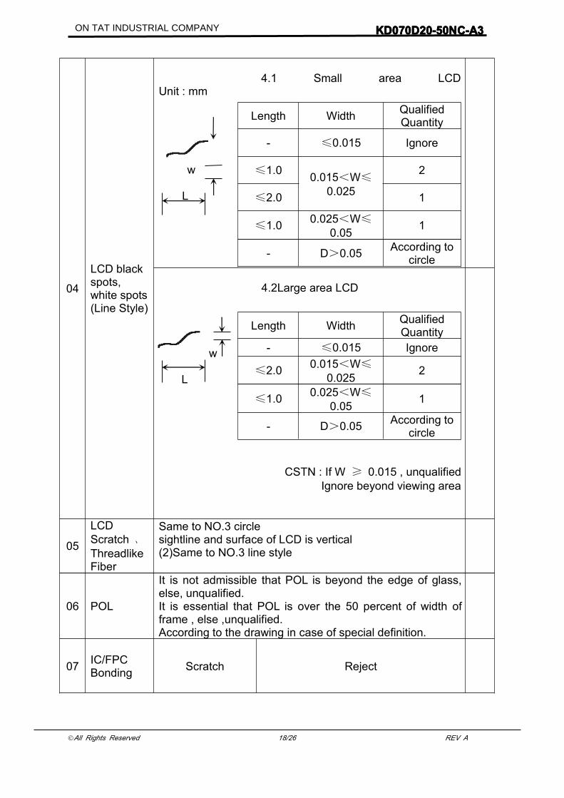
04
LCD blackspots,white spots(Line Style)
4.1 Small area LCDUnit : mm
w
L
Length Width QualifiedQuantity
- ≤0.015 Ignore
≤1.0 0.015<W≤0.025
2
≤2.0 1
≤1.0 0.025<W≤0.05 1
- D>0.05 According tocircle
4.2Large area LCD
w
L
CSTN : If W ≥ 0.015 , unqualifiedIgnore beyond viewing area
Length Width QualifiedQuantity
- ≤0.015 Ignore
≤2.0 0.015<W≤0.025 2
≤1.0 0.025<W≤0.05 1
- D>0.05 According tocircle
05
LCDScratch 、ThreadlikeFiber
Same to NO.3 circlesightline and surface of LCD is vertical(2)Same to NO.3 line style
06 POL
It is not admissible that POL is beyond the edge of glass,else, unqualified.It is essential that POL is over the 50 percent of width offrame , else ,unqualified.According to the drawing in case of special definition.
07 IC/FPCBonding Scratch Reject
ON TAT INDUSTRIAL COMPANY
KD0KD0KD0KD077770D0D0D0D22220000-50N-50N-50N-50NCCCC----A3A3A3A3
©All Rights Reserved 19/26 REV A
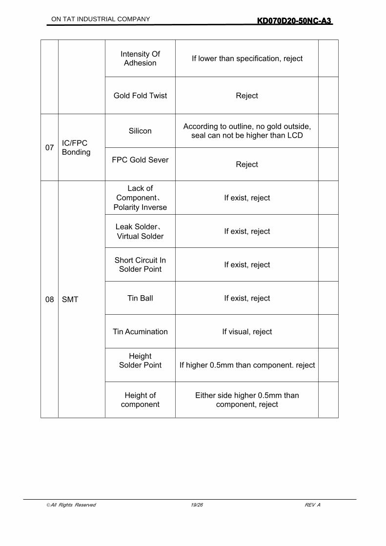
Intensity OfAdhesion If lower than specification, reject
Gold Fold Twist Reject
07 IC/FPCBonding
Silicon According to outline, no gold outside,seal can not be higher than LCD
FPC Gold Sever Reject
08 SMT
Lack ofComponent、
Polarity InverseIf exist, reject
Leak Solder、Virtual Solder If exist, reject
Short Circuit InSolder Point If exist, reject
Tin Ball If exist, reject
Tin Acumination If visual, reject
HeightSolder Point If higher 0.5mm than component. reject
Height ofcomponent
Either side higher 0.5mm thancomponent, reject
ON TAT INDUSTRIAL COMPANY

KD0KD0KD0KD077770D0D0D0D22220000-50N-50N-50N-50NCCCC----A3A3A3A3
©All Rights Reserved 20/26 REV A
Component Shift
X Solder Padcomponent
D Y
Z
X<3/4Z rejecty>1/3D reject
08 SMT
Few Tin
θ pad
PCB
If θ≤20° reject
ComponentDeflection
If Y >1/3D reject
ComponentCarcass
SidewaysReject
CCCComponentomponentomponentomponentDDDD
PadPadPadPadYYYY
ON TAT INDUSTRIAL COMPANY

KD0KD0KD0KD077770D0D0D0D22220000-50N-50N-50N-50NCCCC----A3A3A3A3
©All Rights Reserved 21/26 REV A
ComponentCarcass
SidewaysIf exist with visual inspection , reject
Lot Tin
A: Tin accrete the solder sidecompletely , hollowly ,Ok
B: Tin accrete the solder sidecompletely , full circle arc , ok
C: Jointing include whole solder side,height of tin>50 percent of height ofcomponent, reject
Few Tin
A: Tin accrete the solder sidecompletely , hollowly ,OkB: height of tin > 1/3 of solder side ofcomponent , okC: height of tin ≤ 1/3 of solder side ofcomponent, reject
08 SMT
Normal
Jointing side
09 Light
Short circuit 、Open circuit Forbid
Quality of CSTNDisplay
1、Rolling strake with visual inspection,forbid2、Differentness of color in viewing areawith visual inspection ( full white、red、green、blue), forbid3 、 Display change with visualinspection , forbid
ON TAT INDUSTRIAL COMPANY

KD0KD0KD0KD077770D0D0D0D22220000-50N-50N-50N-50NCCCC----A3A3A3A3
©All Rights Reserved 22/26 REV A
10Color OfCIECoordinate According to the specification
or sample customer haveapproved
x ywhite ±0.05 ±0.05
Red ±0.05 ±0.05
Green ±0.05 ±0.05Blue ±0.05 ±0.05
Drive LCD under normalcondition, 25℃ Φ=0 θ=0Test white、red、green bluewith DMS Record
11 BrightnessIn accord with
productspecification
Drive condition is according tospecificationMeasure location is in Follow Picture3、Adjust brightness instrument tozero ,burrow against the surface of LCD ,press “measure” , record when thedisplay is steady.
(YOKOGAWA-3298)
Measure location
12 CR (Max) According tospecification
According to product specificationMeasure instrument ( DMS-501 )
13 Responsetime
According tospecification
According to product specificationMeasure instrument ( DMS-501 )
14 Viewingangle
According tospecification
According to product specificationMeasure instrument ( DMS-501 )
15 Vibration、Ring
Compare with thesample customer
supply
Compare with the sample customersupply when assemble
16FrequencyOf FPCBend
According to theuse of product( main FPC offoldaway cellphone ≥6thousand )
Measure instrumentBend angle : 150°
Fix FPC in the casement whencustomer supply
ON TAT INDUSTRIAL COMPANY

KD0KD0KD0KD077770D0D0D0D22220000-50N-50N-50N-50NCCCC----A3A3A3A3
©All Rights Reserved 23/26 REV A
9999 HandlingHandlingHandlingHandling PrecautionsPrecautionsPrecautionsPrecautions
9999.1.1.1.1 MountingMountingMountingMounting methodmethodmethodmethodThe LCD panel of Daxian LCD module consists of two thin glass plates with
polarizes which easily be damaged. And since the module in so constructed as tobe fixed by utilizing fitting holes in the printed circuit board.
Extreme care should be needed when handling the LCD modules.
9999.2.2.2.2 CautionCautionCautionCaution ofofofof LCDLCDLCDLCD handlinghandlinghandlinghandling andandandand cleaningcleaningcleaningcleaningWhen cleaning the display surface, Use soft cloth with solvent[recommended below] and wipe lightly
� Isopropyl alcohol� Ethyl alcohol
Do not wipe the display surface with dry or hard materials that will damage thepolarizer surface.
Do not use the following solvent:� Water� Aromatics
Do not wipe ITO pad area with the dry or hard materials that will damage theITO patterns
Do not use the following solvent on the pad or prevent it from beingcontaminated:� Soldering flux� Chlorine (Cl) , Salfur (S)
If goods were sent without being sili8con coated on the pad, ITO patterns couldbe damaged due to the corrosion as time goes on.
If ITO corrosion happen by miss-handling or using some materials such asChlorine (CI), Salfur (S) from customer, Responsibility is on customer.
9999.3.3.3.3 CautionCautionCautionCaution againstagainstagainstagainst staticstaticstaticstatic chargechargechargechargeThe LCD module use C-MOS LSI drivers, so we recommended that you:
Connect any unused input terminal to Vdd or Vss, do not input any signalsbefore power is turned on, and ground your body, work/assembly areas, assemblyequipment to protect against static electricity.
9999.4.4.4.4 packingpackingpackingpacking� Module employ LCD elements and must be treated as such.� Avoid intense shock and falls from a height.� To prevent modules from degradation, do not operate or store them exposed
direct to sunshine or high temperature/humidity
9999.5.5.5.5 CautionCautionCautionCaution forforforfor operationoperationoperationoperation� It is an indispensable condition to drive LCD’s within the specified voltage limit
since the higher voltage then the limit cause the shorter LCD life.� An electrochemical reaction due to direct current causes LCD’s undesirable
deterioration, so that the use of direct current drive should be avoided.� Response time will be extremely delayed at lower temperature then the
operating temperature range and on the other hand at higher temperatureLCD’s how dark color in them. However those phenomena do not mean
ON TAT INDUSTRIAL COMPANY

KD0KD0KD0KD077770D0D0D0D22220000-50N-50N-50N-50NCCCC----A3A3A3A3
©All Rights Reserved 24/26 REV A
malfunction or out of order with LCD’s, which will come back in the specifiedoperation temperature.
� If the display area is pushed hard during operation, some font will beabnormally displayed but it resumes normal condition after turning off once.
� A slight dew depositing on terminals is a cause for electro-chemical reactionresulting in terminal open circuit.
Usage under the maximum operating temperature, 50%Rh or less isrequired.
9999....6666 storagestoragestoragestorageIn the case of storing for a long period of time for instance, for years for the
purpose or replacement use, the following ways are recommended.�Storage in a polyethylene bag with the opening sealed so as not to enter fresh
air outside in it . And with no desiccant.�Placing in a dark place where neither exposure to direct sunlight nor light’s
keeping the storage temperature range.�Storing with no touch on polarizer surface by the anything else.
[It is recommended to store them as they have been contained in the innercontainer at the time of delivery from us
9999....7777 SafetySafetySafetySafety
� It is recommendable to crash damaged or unnecessary LCD’s into pieces andwash off liquid crystal by either of solvents such as acetone and ethanol, whichshould be burned up later.�When any liquid leaked out of a damaged glass cell comes in contact with your
hands, please wash it off well with soap and water
10101010 PrecaPrecaPrecaPrecautionutionutionution forforforfor useuseuseuse
10.110.110.110.1
A limit sample should be provided by the both parties on an occasion when theboth parties agreed its necessity. Judgment by a limit sample shall take effect afterthe limit sample has been established and confirmed by the both parties.
10.210.210.210.2
On the following occasions, the handing of problem should be decided throughdiscussion and agreement between responsible of the both parties.�When a question is arisen in this specification�When a new problem is arisen which is not specified in this specifications�When an inspection specifications change or operating condition change in
customer is reported , and some problem is arisen in this specification due tothe change.�When a new problem is arisen at the customer’s operating set for sample
evaluation in the customer site.
ON TAT INDUSTRIAL COMPANY

KD0KD0KD0KD077770D0D0D0D22220000-50N-50N-50N-50NCCCC----A3A3A3A3
©All Rights Reserved 25/26 REV A
11111111DiDiDiDimensionalmensionalmensionalmensional OutlineOutlineOutlineOutline
TTTLE
:
REV
版本
A00
DESCRIP
TION
描述
First is
sue
DATE 日
期
2013-03-21
LED电
路图
A K
谢健
彬20
13-0
3-21
KD0
70D2
0-50
NC-A
3
LCM
高温
胶
ON TAT INDUSTRIAL COMPANY
ON
TA
T IN
DU
ST
RIA
L C
OM
PA
NY

KD0KD0KD0KD077770D0D0D0D22220000-50N-50N-50N-50NCCCC----A3A3A3A3
©All Rights Reserved 26/26 REV A
12.12.12.12. PackagePackagePackagePackage DrawingDrawingDrawingDrawingTBDTBDTBDTBD
ON TAT INDUSTRIAL COMPANY