d1 version draft - whycan.com
TRANSCRIPT
Copyright© Allwinner Technology Co.,Ltd. All Rights Reserved
D1 The RISC-V Multi-Media Decoding Platform SoC
Features XuanTie C906 RISC-V CPU HiFi4 DSP Memories
- DDR2/DDR3 SDRAM - SD3.0/SDIO3.0/eMMC5.0
Video Engine - H.265/H.264/MPEG-1/2/4/JPEG/VC1 decoding, up to 4K - JPEG/MJPEG encoding, up to 1080p@60fps
Video and Graphics - Allwinner SmartColor2.0 post processing for an excellent display experience - Supports de-interlace (DI) up to 1080p@60fps - Supports Graphic 2D (G2D) hardware accelerator including rotate, mixer, LBC decompression functions
Video Output - RGB interface up to 1920 x 1080@60fps - Dual link LVDS interface up to 1920 x 1080@60fps - 4-lane MIPI DSI up to 1920 x 1200@60fps - HDMI TX interface up to 4K@30fps - CVBS OUT interface, supporting NTSC and PAL format
Video Input - 8-bit parallel CSI interface - CVBS IN interface, supporting NTSC and PAL format
Analog Audio Codec - 2 DACs and 3 ADCs - Analog audio interfaces: LINEOUTLP/N, LINEOUTRP/N, HPOUTL/R, MICIN1P/1N, MICIN2P/2N, MICIN3P/3N,
LINEINL/R, FMINL/R Three I2S/PCM external interfaces (I2S0, I2S1, I2S2) Maximum 8 digital PDM microphones (DMIC) OWA TX and OWA RX, compliance with S/PDIF interface Security System
- AES, DES, 3DES, RSA, MD5, SHA, HMAC - Integrated 2 Kbits OTP storage space
External Peripherals - USB 2.0 DRD (USB0) and USB 2.0 HOST (USB1) - 10/100/1000 Mbps Ethernet port with RGMII and RMII interfaces - Up to 6 UART controllers (UART0, UART1, UART2, UART3, UART4, UART5) - Up to 2 SPI controllers (SPI0, SPI1) - Up to 4 TWI controllers (TWI0, TWI1, TWI2, TWI3) - CIR RX and CIR TX - 8 independent PWM channels (PWM0 to PWM7) - 2-ch GPADC - 4-ch TPADC - 1-ch LRADC - LEDC
Package - LFBGA 337 balls, 13 mm x 13 mm
Draft Versio
n

Confidential
Copyright© Allwinner Technology Co.,Ltd. All Rights Reserved. i
Revision History
Revision Date Author Description
0.1 March 02, 2021 AWAXXXX Draft version
Draft Versio
n
Confidential
Copyright© Allwinner Technology Co.,Ltd. All Rights Reserved. ii
Contents
The RISC-V Multi-Media Decoding Platform SoC .................................................................................................................. i
Revision History..................................................................................................................................................................... i
Contents ............................................................................................................................................................................... ii
Figures ................................................................................................................................................................................. vi
Tables ................................................................................................................................................................................ viii
About This Documentation ..................................................................................................................................................1
1 Overview ......................................................................................................................................................................3
2 Features ........................................................................................................................................................................4
2.1 CPU Architecture ..................................................................................................................................................4
2.2 DSP Architecture ..................................................................................................................................................4
2.3 Memory Subsystem..............................................................................................................................................4
2.3.1 Boot ROM (BROM) ...............................................................................................................................4
2.3.2 SDRAM .................................................................................................................................................4
2.3.3 SMHC ....................................................................................................................................................4
2.4 Video Engine ........................................................................................................................................................5
2.5 Video and Graphics ..............................................................................................................................................5
2.5.1 Display Engine (DE)...............................................................................................................................5
2.5.2 De-interlacer (DI) ..................................................................................................................................6
2.5.3 Graphic 2D (G2D) .................................................................................................................................6
2.6 Video Output .......................................................................................................................................................7
2.6.1 RGB and LVDS LCD ................................................................................................................................7
2.6.2 MIPI DSI ................................................................................................................................................7
2.6.3 HDMI ....................................................................................................................................................7
2.6.4 CVBS OUT .............................................................................................................................................8
2.7 Video Input ..........................................................................................................................................................8
2.7.1 Parallel CSI ............................................................................................................................................8
2.7.2 CVBS IN .................................................................................................................................................8
2.8 System Peripherals ...............................................................................................................................................9
2.8.1 Timer ....................................................................................................................................................9
2.8.2 High Speed Timer (HSTimer) ................................................................................................................9
Draft Versio
n

Confidential
Copyright© Allwinner Technology Co.,Ltd. All Rights Reserved. iii
2.8.3 Platform-Level Interrupt Controller (PLIC) ...........................................................................................9
2.8.4 DMAC ...................................................................................................................................................9
2.8.5 Clock Controller Unit (CCU) ............................................................................................................... 10
2.8.6 Thermal Sensor Controller (THS) ....................................................................................................... 10
2.8.7 LDO Power ......................................................................................................................................... 10
2.8.8 RTC .................................................................................................................................................... 10
2.8.9 Reset .................................................................................................................................................. 11
2.9 Audio Subsystem ............................................................................................................................................... 11
2.9.1 Audio Codec ...................................................................................................................................... 11
2.9.2 I2S/PCM ............................................................................................................................................. 12
2.9.3 DMIC .................................................................................................................................................. 12
2.9.4 One Wire Audio (OWA) ..................................................................................................................... 12
2.10 External Peripherals .......................................................................................................................................... 14
2.10.1 USB DRD ............................................................................................................................................ 14
2.10.2 USB HOST .......................................................................................................................................... 14
2.10.3 EMAC ................................................................................................................................................. 15
2.10.4 UART .................................................................................................................................................. 15
2.10.5 SPI and SPI_DBI ................................................................................................................................. 16
2.10.6 Two Wire Interface (TWI) ...................................................................................................................17
2.10.7 CIR Receiver (CIR_RX) .........................................................................................................................17
2.10.8 CIR Transmitter (CIR_TX) ....................................................................................................................17
2.10.9 PWM ...................................................................................................................................................17
2.10.10 General Purpose ADC (GPADC) ......................................................................................................... 18
2.10.11 Touch Panel ADC (TPADC) ................................................................................................................. 18
2.10.12 Low Rate ADC (LRADC) ...................................................................................................................... 19
2.10.13 LEDC .................................................................................................................................................. 19
2.11 Package ............................................................................................................................................................. 19
3 Block Diagram ............................................................................................................................................................20
4 Pin Description .......................................................................................................................................................... 22
4.1 Pin Quantity ...................................................................................................................................................... 22
4.2 Pin Characteristics ............................................................................................................................................. 22
4.3 GPIO Multiplex Function ................................................................................................................................... 35
4.4 Detailed Signal Description ............................................................................................................................... 39
5 Electrical Characteristics ............................................................................................................................................52
Draft Versio
n
Confidential
Copyright© Allwinner Technology Co.,Ltd. All Rights Reserved. iv
5.1 Parameter Conditions ........................................................................................................................................52
5.1.1 Minimum and Maximum Values ........................................................................................................52
5.1.2 Typical Values .....................................................................................................................................52
5.1.3 Temperature Definitions ....................................................................................................................52
5.2 Absolute Maximum Ratings ...............................................................................................................................52
5.3 Recommended Operating Conditions ............................................................................................................... 54
5.4 Power Consumption Parameters ...................................................................................................................... 56
5.5 DC Electrical Characteristics .............................................................................................................................. 58
5.6 SDIO Electrical Characteristics ........................................................................................................................... 58
5.7 GPADC Electrical Characteristics ....................................................................................................................... 60
5.8 LRADC Electrical Characteristics ........................................................................................................................ 60
5.9 Audio Codec Electrical Characteristics .............................................................................................................. 61
5.10 External Clock Source Characteristics ............................................................................................................... 63
5.10.1 High-speed Crystal/Ceramic Resonator Characteristics .................................................................... 63
5.10.2 Low-speed Crystal/Ceramic Resonator Characteristics ..................................................................... 64
5.11 Internal Reset Electrical Characteristics ............................................................................................................ 65
5.12 External Memory Electrical Characteristics ...................................................................................................... 65
5.12.1 SMHC AC Electrical Characteristics ................................................................................................... 65
5.13 External Peripheral Electrical Characteristics .....................................................................................................73
5.13.1 EMAC AC Electrical Characteristics .....................................................................................................73
5.13.2 SPI AC Electrical Characteristics ........................................................................................................ 75
5.13.3 UART AC Electrical Characteristics ..................................................................................................... 76
5.13.4 TWI AC Electrical Characteristics ........................................................................................................78
5.13.5 I2S/PCM AC Electrical Characteristics ............................................................................................... 79
5.13.6 DMIC AC Electrical Characteristics .................................................................................................... 80
5.13.7 OWA AC Electrical Characteristics ..................................................................................................... 81
5.13.8 CIR_RX AC Electrical Characteristics .................................................................................................. 81
5.14 Power-On and Power-Off Sequence ...................................................................................................................82
5.14.1 Power-On Sequence ...........................................................................................................................82
5.14.2 Power-Off Sequence ...........................................................................................................................82
6 Package Thermal Characteristics ............................................................................................................................... 84
7 Pin Assignment .......................................................................................................................................................... 85
7.1 Pin Map ............................................................................................................................................................. 85
7.2 Package Dimension ........................................................................................................................................... 86
Draft Versio
n

Confidential
Copyright© Allwinner Technology Co.,Ltd. All Rights Reserved. v
8 Carrier, Storage and Baking Information .................................................................................................................... 87
8.1 Carrier ................................................................................................................................................................ 87
8.1.1 Matrix Tray Information ..................................................................................................................... 87
8.2 Storage .............................................................................................................................................................. 88
8.2.1 Moisture Sensitivity Level (MSL) ....................................................................................................... 88
8.2.2 Bagged Storage Conditions ............................................................................................................... 89
8.2.3 Out-of-bag Duration .......................................................................................................................... 89
8.3 Baking ................................................................................................................................................................ 89
9 Reflow Profile ............................................................................................................................................................ 91
10 FT/QA/QC Test ........................................................................................................................................................... 93
10.1 FT Test ............................................................................................................................................................... 93
10.2 QA Test .............................................................................................................................................................. 93
10.3 QC Test .............................................................................................................................................................. 93
11 Part Marking .............................................................................................................................................................. 94
Draft Versio
n
Confidential
Copyright© Allwinner Technology Co.,Ltd. All Rights Reserved. vi
Figures
Figure 3-1 D1 System Block Diagram .................................................................................................................................. 20
Figure 3-2 D1 Multi-Media Decoding Platform Solution .................................................................................................... 21
Figure 5-1 SDIO Voltage Waveform .................................................................................................................................... 59
Figure 5-2 SMHC HS-SDR Mode Output Timing Diagram ................................................................................................... 66
Figure 5-3 SMHC HS-SDR Mode Input Timing Diagram ...................................................................................................... 66
Figure 5-4 SMHC HS-DDR Mode Output Timing Diagram ................................................................................................... 67
Figure 5-5 SMHC HS-DDR Mode Input Timing Diagram ...................................................................................................... 68
Figure 5-6 SMHC HS200 Mode Output Timing Diagram ..................................................................................................... 69
Figure 5-7 SMHC HS200 Mode Input Timing Diagram ........................................................................................................ 70
Figure 5-8 SMHC HS400 Data Output Timing Diagram ....................................................................................................... 71
Figure 5-9 SMHC HS400 Data Input Timing Diagram .......................................................................................................... 72
Figure 5-10 RGMII Interface Transmit Timing ..................................................................................................................... 73
Figure 5-11 RGMII Interface Receive Timing....................................................................................................................... 74
Figure 5-12 RMII Interface Transmit Timing ....................................................................................................................... 74
Figure 5-13 RMII Interface Receive Timing ......................................................................................................................... 75
Figure 5-14 SPI Writing Timing ............................................................................................................................................ 75
Figure 5-15 SPI Reading Timing ........................................................................................................................................... 76
Figure 5-16 UART RX Timing ............................................................................................................................................... 76
Figure 5-17 UART nCTS Timing ............................................................................................................................................ 77
Figure 5-18 UART nRTS Timing ............................................................................................................................................ 77
Figure 5-19 TWI Timing ....................................................................................................................................................... 78
Figure 5-20 I2S/PCM Timing in Master Mode ..................................................................................................................... 79
Figure 5-21 I2S/PCM Timing in Slave Mode ........................................................................................................................ 79
Figure 5-22 DMIC Timing .................................................................................................................................................... 80
Figure 5-23 OWA Timing ..................................................................................................................................................... 81
Figure 5-24 CIR_RX Timing .................................................................................................................................................. 81
Figure 5-25 Power-On Timing ............................................................................................................................................. 82
Figure 5-26 Power-Off Timing ............................................................................................................................................. 83
Figure 7-1 D1 Pin Map ......................................................................................................................................................... 85
Figure 7-2 D1 Package Dimension ....................................................................................................................................... 86
Draft Versio
n

Confidential
Copyright© Allwinner Technology Co.,Ltd. All Rights Reserved. vii
Figure 8-1 D1 Tray Dimension Drawing .............................................................................................................................. 88
Figure 9-1 Lead-free Reflow Profile .................................................................................................................................... 91
Figure 9-2 Measuring the Reflow Soldering Process .......................................................................................................... 92
Figure 11-1 D1 Marking....................................................................................................................................................... 94
Draft Versio
n
Confidential
Copyright© Allwinner Technology Co.,Ltd. All Rights Reserved. viii
Tables
Table 4-1 D1 Pin Quantity ................................................................................................................................................... 22
Table 4-2 Pin Characteristics ............................................................................................................................................... 23
Table 4-3 GPIO Multiplex Function ..................................................................................................................................... 35
Table 4-4 Detailed Signal Description ................................................................................................................................. 39
Table 5-1 Absolute Maximum Ratings ................................................................................................................................ 53
Table 5-2 Recommended Operating Conditions ................................................................................................................. 54
Table 5-3 Power Consumption Parameters ........................................................................................................................ 56
Table 5-4 DC Electrical Characteristics ................................................................................................................................ 58
Table 5-5 3.3 V SDIO Electrical Parameters ........................................................................................................................ 59
Table 5-6 1.8 V SDIO Electrical Parameters ........................................................................................................................ 59
Table 5-7 GPADC Electrical Characteristics ......................................................................................................................... 60
Table 5-8 LRADC Electrical Characteristics .......................................................................................................................... 60
Table 5-9 Audio Codec Typical Performance Parameters ................................................................................................... 61
Table 5-10 High-speed 24 MHz Crystal Circuit Characteristics ........................................................................................... 63
Table 5-11 Crystal Circuit Parameters ................................................................................................................................. 63
Table 5-12 Low-speed 32.768 kHz Crystal Circuit Characteristics ...................................................................................... 64
Table 5-13 Internal Reset Electrical Characteristics ............................................................................................................ 65
Table 5-14 SMHC HS-SDR Mode Output Timing Constants ................................................................................................ 66
Table 5-15 SMHC HS-SDR Mode Input Timing Constants ................................................................................................... 66
Table 5-16 SMHC HS-DDR Mode Output Timing Constants ............................................................................................... 67
Table 5-17 SMHC HS-DDR Mode Input Timing Constants .................................................................................................. 68
Table 5-18 SMHC HS200 Mode Output Timing Constants .................................................................................................. 69
Table 5-19 SMHC HS200 Mode Input Timing Constants ..................................................................................................... 70
Table 5-20 SMHC HS400 Output Timing Parameters .......................................................................................................... 71
Table 5-21 SMHC HS400 Data Input Timing Parameter ...................................................................................................... 72
Table 5-22 RGMII Transmit Timing Constants .................................................................................................................... 73
Table 5-23 RGMII Receive Timing Constants ...................................................................................................................... 74
Table 5-24 RMII Transmit Timing Constants ....................................................................................................................... 75
Table 5-25 RMII Receive Timing Constants ......................................................................................................................... 75
Table 5-26 SPI Timing Constants ......................................................................................................................................... 76
Draft Versio
n
Confidential
Copyright© Allwinner Technology Co.,Ltd. All Rights Reserved. ix
Table 5-27 UART Timing Constants ..................................................................................................................................... 77
Table 5-28 TWI Timing Parameters ..................................................................................................................................... 78
Table 5-29 I2S/PCM Timing Constants in Master Mode ..................................................................................................... 79
Table 5-30 I2S/PCM Timing Constants in Slave Mode ........................................................................................................ 80
Table 5-31 DMIC Timing Constants ..................................................................................................................................... 80
Table 5-32 OWA Timing Constants ..................................................................................................................................... 81
Table 5-33 CIR_RX Timing Constants .................................................................................................................................. 81
Table 6-1 D1 Package Thermal Characteristics ................................................................................................................... 84
Table 8-1 Matrix Tray Carrier Information .......................................................................................................................... 87
Table 8-2 D1 Packing Quantity Information ........................................................................................................................ 87
Table 8-3 MSL Summary ..................................................................................................................................................... 88
Table 8-4 Bagged Storage Conditions ................................................................................................................................. 89
Table 8-5 Out-of-bag Duration ............................................................................................................................................ 89
Table 9-1 Lead-free Reflow Profile Conditions ................................................................................................................... 91
Table 11-1 D1 Marking Definitions ..................................................................................................................................... 94 Draft Versio
n
Confidential
Copyright© Allwinner Technology Co.,Ltd. All Rights Reserved. 1
About This Documentation
Purpose
The documentation describes features of each module, pin/signal characteristics, current consumption,
interface timing, thermal and package, and part reliability of the D1 processor. For details about register
descriptions of each module, see the D1_User_Manual.
Intended Audience
The document is intended for:
Hardware designers and maintenance personnel for electronics
Sales personnel for electronic parts and components
Conventions
Symbol Conventions
The symbols that may be found in this document are defined as follows.
Symbol Description
Indicates potential risk of injury or death exists if the instructions are not obeyed.
Indicates potential risk of equipment damage, data loss, performance
degradation, or unexpected results exists if the instructions are not obeyed.
Provides additional information to emphasize or supplement important points of
the main text.
Table Content Conventions
The table content conventions that may be found in this document are defined as follows.
Symbol Description
- The cell is blank.
Numerical Conventions
The expressions of data capacity, frequency, and data rate are described as follows.
NOTE
CAUTION
WARNING
Draft Versio
n
Confidential
Copyright© Allwinner Technology Co.,Ltd. All Rights Reserved. 2
Type Symbol Value
Data capacity
1K 1024
1M 1,048,576
1G 1,073,741,824
Frequency, data rate
1k 1000
1M 1,000,000
1G 1,000,000,000
Draft Versio
n

Confidential
Copyright© Allwinner Technology Co.,Ltd. All Rights Reserved. 3
1 Overview D1 is an advanced application processor designed for RISC-V Multi-Media decoding platform. It integrates a
64-bit XuanTie C906 RISC-V CPU and a HiFi4 DSP to provide the high-efficient computing power. D1 supports
full format decoding such as H.265, H.264, MPEG-1/2/4, JPEG, VC1, and so on. The independent encoder can
encode in JPEG or MJPEG. Integrated multi ADCs/DACs and I2S/PCM/DMIC/OWA audio interfaces can work
seamlessly with the CPU to accelerate multimedia algorithms and improve the user experience. D1 supports
RGB/LVDS/MIPI DSI/HDMI/CVBS OUT display output interfaces to meet the requirements of the different
screen display. D1 comes with extensive connectivity and interfaces, such as USB, SDIO, EMAC, TWI, UART, SPI,
PWM, GPADC, LRADC, TPADC, IR TX&RX, and so on. Besides, D1 can connect with other different peripherals
like WiFi and BT via SDIO and UART.
Draft Versio
n
Confidential
Copyright© Allwinner Technology Co.,Ltd. All Rights Reserved. 4
2 Features
2.1 CPU Architecture
• XuanTie C906 RISC-V CPU
• 32 KB I-cache + 32 KB D-cache
2.2 DSP Architecture
• HiFi4
• 32 KB L1 I-cache and 32 KB L1 D-cache
• 64 KB I-ram and 64 KB D-ram
2.3 Memory Subsystem
2.3.1 Boot ROM (BROM)
• On-chip memory
• Supports system boot from the following devices:
- SD card
- eMMC
- SPI NOR Flash
- SPI NAND Flash
• Supports mandatory upgrade process through USB and SD card
• Supports GPIO pin and eFuse module to select the boot media type
2.3.2 SDRAM
• Supports DDR2/DDR3 SDRAM
• Maximum capacity up to 2 GB
• Supports clock frequency up to 533 MHz for DDR2
• Supports clock frequency up to 800 MHz for DDR3
2.3.3 SMHC
• Three SD/MMC host controller (SMHC) interfaces
• The SMHC0 controls the devices that comply with the protocol Secure Digital Memory (SD mem-version
3.0)
Draft Versio
n

Confidential
Copyright© Allwinner Technology Co.,Ltd. All Rights Reserved. 5
• The SMHC1 controls the device that complies with the protocol Secure Digital I/O (SDIO-version 3.0)
• The SMHC2 controls the device that complies with the protocol Multimedia Card (eMMC-version 5.0)
• Maximum performance:
- SDR mode 150 [email protected] V IO pad
- DDR mode 100 [email protected] V IO pad
- DDR mode 50 [email protected] V IO pad
• Supports 1-bit or 4-bit data width
• Supports block size of 1 to 65535 bytes
• Internal 1024-Bytes RX FIFO and 1024-Bytes TX FIFO
• Supports card insertion and removal interrupt
• Supports hardware CRC generation and error detection
• Supports descriptor-based internal DMA controller
2.4 Video Engine
• Video decoding
- H.265 [email protected] up to 4K@30fps or 1080p@60fps
- H.264 BP/MP/[email protected] up to 4K@24fps or 1080p@60fps
- H.263 BP up to 1080p@60fps
- MPEG-4 SP/ASP L5 up to 1080p@60fps
- MPEG-2 MP/HL up to 1080p@60fps
- MPEG-1 MP/HL up to 1080p@60fps
- Xvid up to 1080p@60fps
- Sorenson Spark up to 1080p@60fps
- WMV9/VC-1 SP/MP/AP up to 1080p@60fps
- MJPEG up to 1080p@30fps
• Video encoding
- JPEG/MJPEG up to 1080p@60fps
- Supports input picture scaler up/down
2.5 Video and Graphics
2.5.1 Display Engine (DE)
• Output size up to 2048 x 2048
Draft Versio
n
Confidential
Copyright© Allwinner Technology Co.,Ltd. All Rights Reserved. 6
• Supports two alpha blending channels for main display and one channel for aux display
• Supports four overlay layers in each channel, and has an independent scaler
• Supports potter-duff compatible blending operation
• Supports LBC buffer decoder
• Supports dither output to TCON
• Supports input format Semi-planar YUV422/YUV420/YUV411 and Planar YUV422/YUV420/YUV411,
ARGB8888/XRGB8888/RGB888/ARGB4444/ARGB1555/RGB565/palette
• Supports SmartColor2.0 for excellent display experience
- Adaptive detail/edge enhancement
- Adaptive color enhancement
- Adaptive contrast enhancement and fresh tone rectify
• Supports write back for aux display
2.5.2 De-interlacer (DI)
• Supports YUV420 (Planar/NV12/NV21) and YUV422 (Planar/NV16/NV61) data format
• Support video resolution from 32x32 to 2048x1280 pixel
• Support Inter-field interpolation/motion adaptive de-interlace method
• Performance: module clock 600M for 1080p@60Hz YUV420
2.5.3 Graphic 2D (G2D)
• Supports layer size up to 2048 x 2048 pixels
• Supports pre-multiply alpha image data
• Supports color key
• Supports two pipes Porter-Duff alpha blending
• Supports multiple video formats 4:2:0, 4:2:2, 4:1:1 and multiple pixel formats (8/16/24/32 bits graphics
layer)
• Supports memory scan order option
• Supports any format convert function
• Supports 1/16× to 32× resize ratio
• Supports 32-phase 8-tap horizontal anti-alias filter and 32-phase 4-tap vertical anti-alias filter
• Supports window clip
• Supports FillRectangle, BitBlit, StretchBlit and MaskBlit
• Supports horizontal and vertical flip, clockwise 0/90/180/270 degree rotate for normal buffer
• Supports horizontal flip, clockwise 0/90/270 degree rotate for LBC buffer
Draft Versio
n
Confidential
Copyright© Allwinner Technology Co.,Ltd. All Rights Reserved. 7
2.6 Video Output
2.6.1 RGB and LVDS LCD
• Supports RGB interface with DE/SYNC mode, up to 1920 x 1080@60fps
• Supports serial RGB/dummy RGB interface, up to 800 x 480@60fps
• Supports LVDS interface with dual link, up to 1920 x 1080@60fps
• Supports LVDS interface with single link, up to 1366 x 768@60fps
• Supports i8080 interface, up to 800 x 480@60fps
• Supports BT656 interface for NTSC and PAL
• RGB888, RGB666 and RGB565 with dither function
• Gamma correction with R/G/B channel independence
2.6.2 MIPI DSI
• Compliance with MIPI DSI v1.01
• Supports 4-lane MIPI DSI, up to 1280 x 720@60fps and 1920 x 1200@60fps
• Supports non-burst mode with sync pulse/sync event, burst mode and command mode
• Supports pixel format: RGB888, RGB666, RGB666 loosely packed and RGB565
• Supports continuous and non-continuous lane clock modes
• Supports bidirectional communication of all generic commands in LP through data lane 0
• Supports low power data transmission
• Supports ULPS and escape modes
• Hardware checksum capabilities
2.6.3 HDMI
• Compatible with HDMI 2.0
• Supports DDC and SCDC
• Integrated CEC hardware engine
• Optional color space converter (CSC): RGB (4:4:4) to/from YCbCr (4:4:4 or 4:2:2)
• Video formats:
- All CEA-861-E video formats up to 1080p at 60 Hz and 720p/1080i at 120 Hz
- Optional HDMI 1.4b video formats
All CEA-861-E video formats up to 1080p at 120 Hz
HDMI 1.4b 4K x 2K video formats
Draft Versio
n

Confidential
Copyright© Allwinner Technology Co.,Ltd. All Rights Reserved. 8
HDMI 1.4b 3D video modes with up to 340 MHz (TMDS clock)
- Optional HDMI 2.0 video formats
All CEA-861-F video formats
Dynamic Range and Mastering InfoFrame (DRM, packet header 0x87)
• Audio formats:
- Uncompressed audio formats: IEC60985 L-PCM audio samples, up to 192 kHz
- Compressed audio formats: IEC61937 compressed audio, up to 1536 kHz (for HDMI 2.0b)/768 kHz
(for HDMI 1.4b)
2.6.4 CVBS OUT
• 1-channel CVBS output
• Supports NTSC and PAL format
• Plug status auto detecting
• 10 bits DAC output
2.7 Video Input
2.7.1 Parallel CSI
• Supports 8-bit digital camera interface (RAW8/YUV422/YUV420)
• Supports BT656, BT601 interface (YUV422)
• Supports ITU-R BT.656 time-multiplexed format up to 2*1080p@30fps in DDR sample mode
• Maximum pixel clock of 148.5 MHz
• Supports de-interlacing for interlace video input
• Supports conversion from YUV422 to YUV420, YUV422 to YUV400, YUV420 to YUV400
• Supports horizontal and vertical flip
2.7.2 CVBS IN
• 2-channel CVBS input and 1-channel CVBS decoder
• Supports NTSC and PAL format
• Supports YUV422/YUV420 format
• With 1 channel 3D comb filter
• Detection for signal locked and 625 lines
• Programmable brightness, contrast, and saturation
• 10-bit video ADCs
Draft Versio
n
Confidential
Copyright© Allwinner Technology Co.,Ltd. All Rights Reserved. 9
2.8 System Peripherals
2.8.1 Timer
• The timer module implements the timing and counting functions, which includes timer0, timer1,
watchdog, and audio video synchronization (AVS)
• The timer0/timer1 is a 32-bit down counter. The timer0 and timer1 are completely consistent
• The watchdog is used to transmit a reset signal to reset the entire system when an exception occurs in
the system
• The AVS is used to synchronize the audio and video. The AVS sub-block includes AVS0 and AVS1, which
are completely consistent
2.8.2 High Speed Timer (HSTimer)
• The HSTimer module consists of HSTimer0 and HSTimer1. HSTimer0 and HSTimer1 are down counters
that implement timing and counting functions. They are completely consistent.
• Configurable 56-bit down timer
• Supports 5 prescale factors
• The clock source is synchronized with AHB0 clock, much more accurate than other timers
• Supports 2 working modes: periodic mode and single counting mode
• Generates an interrupt when the count is decreased to 0
2.8.3 Platform-Level Interrupt Controller (PLIC)
• Sampling, priority arbitration and distribution for external interrupt sources
• The interrupt can be configured as machine mode and super user mode
• Up to 256 interrupt source sampling, supporting level interrupt and pulse interrupt
• 32 levels of interrupt priority
• Maintains independently the interrupt enable for each interrupt mode (machine/super user)
• Maintains independently the interrupt threshold for each interrupt mode (machine/super user)
• Configurable access permission for PLIC registers
2.8.4 DMAC
• Up to 16-ch DMA
• Provides 32 peripheral DMA requests for data reading and 32 peripheral DMA requests for data writing
• Flexible data width of 8/16/32/64-bit
• Programmable DMA burst length
• Supports linear and IO address modes
Draft Versio
n
Confidential
Copyright© Allwinner Technology Co.,Ltd. All Rights Reserved. 10
• Supports data transfer types with memory-to-memory, memory-to-peripheral, peripheral-to-memory,
peripheral-to-peripheral
• Supports transferring data with a linked list
• DRQ response includes waiting mode and handshake mode
• DMA channel supports pause function
• Memory devices support non-aligned transform
2.8.5 Clock Controller Unit (CCU)
• 8 PLLs
• One on-chip RC oscillator
• Supports one external 24 MHz DCXO and one external 32.768 kHz oscillator
• Supports clock configuration and clock generation for corresponding modules
• Supports software-controlled clock gating and software-controlled reset for corresponding modules
2.8.6 Thermal Sensor Controller (THS)
• One thermal sensor located in CPU
• Temperature accuracy: ±3°C from 0°C to +100°C, ±5°C from -25°C to +125°C
• Averaging filter for thermal sensor reading
• Supports over-temperature protection interrupt and over-temperature alarm interrupt
2.8.7 LDO Power
• Integrated 2 LDOs (LDOA, LDOB)
• LDOA: 1.8 V power output, LDOB: 1.35 V/1.5 V/1.8 V power output
• LDOA for IO and analog module, LDOB for SDRAM
• Input voltage is 2.4 V to 3.6 V
2.8.8 RTC
• Implements time counter and timing wakeup
• Provides a 16-bit counter for counting day, 5-bit counter for counting hour, 6-bit counter for counting
minute, 6-bit counter for counting second
• External connect a 32.768 kHz low-frequency oscillator for count clock
• Timer frequency is 1 kHz
• Configurable initial value by software anytime
Draft Versio
n

Confidential
Copyright© Allwinner Technology Co.,Ltd. All Rights Reserved. 11
• Supports timing alarm, and generates interrupt and wakeup the external devices
• 8 general purpose registers for storing power-off information
2.8.9 Reset
• Integrated internal reset
• Reset D1 or other IC
2.9 Audio Subsystem
2.9.1 Audio Codec
• Two audio digital-to-analog (DAC) channels
- Supports 16-bit and 20-bit sample resolution
- 8 kHz to 192 kHz DAC sample rate
- 100 ± 2 dB SNR@A-weight, -85 ± 3 dB THD+N
• Two audio outputs:
- One stereo headphone output: HPOUTL/R
- One stereo differential lineout output: LINEOUTLP/N and LINEOUTRP/N
• Three audio analog-to-digital (ADC) channels
- Supports 16-bit and 20-bit sample resolution
- 8 kHz to 48 kHz ADC sample rate
- 95 ± 3dB SNR@A-weight, -80 ± 3dB THD+N
• Five audio inputs:
- Three differential microphone inputs: MICIN1P/1N, MICIN2P/2N, MICIN3P/3N
- One stereo LINEIN input: LINEINL/R
- One stereo FMIN input: FMINL/R
• Stereo headphone driver
- 95 ± 3 dB SNR@A-weight
- Output Level 0.55 Vrms@10 kΩ/THD+N -77 ± 3 dB, 0.37 Vrms@16 Ω/THD+N -40 dB
• Supports Dynamic Range Controller adjusting the DAC playback and ADC recording
• One 128x20-bits FIFO for DAC data transmit, one 128x20-bits FIFO for ADC data receive
• Programmable FIFO thresholds
• Supports interrupts and DMA
Draft Versio
n
Confidential
Copyright© Allwinner Technology Co.,Ltd. All Rights Reserved. 12
2.9.2 I2S/PCM
• Three I2S/PCM external interfaces (I2S0, I2S1, I2S2) for connecting external power amplifier and MIC
ADC
• Compliant with standard Philips Inter-IC sound (I2S) bus specification
- Left-justified, Right-justified, PCM mode, and Time Division Multiplexing (TDM) format
- Programmable PCM frame width: 1 BCLK width (short frame) and 2 BCLKs width (long frame)
• Transmit and Receive data FIFOs
- Programmable FIFO thresholds
- 128 depth x 32-bit width TXFIFO and 64 depth x 32-bit width RXFIFO
• Supports multiple function clock
- Clock up to 24.576 MHz Data Output of I2S/PCM in Master mode (Only if the IO PAD and Peripheral
I2S/PCM satisfy Timing Parameters)
- Clock up to 12.288 MHz Data Input of I2S/PCM in Master mode
• Supports TX/RX DMA slave interface
• Supports multiple application scenarios
- Up to 16 channels (fs = 48 kHz) which has adjustable width from 8-bit to 32-bit
- Sample rate from 8 kHz to 384 kHz (CHAN = 2)
- 8-bit u-law and 8-bit A-law companded sample
• Supports master/slave mode
2.9.3 DMIC
• Supports maximum 8 digital PDM microphones
• Supports sample rate from 8 kHz to 48 kHz
2.9.4 One Wire Audio (OWA)
• One OWA TX and one OWA RX
• Compliance with S/PDIF interface
• IEC-60958 and IEC-61937 transmitter and receiver functionality
- IEC-60958 supports 16-bit, 20-bit, and 24-bit data formats
- IEC-61937 uses the IEC-60958 series for the conveying of non-linear PCM bit streams, each
sub-frame transmits 16-bit
• TXFIFO and RXFIFO
- One 128×24bits TXFIFO and one 64×24bits RXFIFO for audio data transfer
- Programmable FIFO thresholds
Draft Versio
n

Confidential
Copyright© Allwinner Technology Co.,Ltd. All Rights Reserved. 13
• Supports TX/RX DMA slave interface
• Supports multiple function clock
- Separate clock for OWA TX and OWA RX
- The clock of TX function includes 24.576 MHz and 22.579 MHz frequency
- The clock of RX function includes 24.576*8MHz frequency
• Supports hardware parity on TX/RX
- Hardware parity checking on the receiver
- Hardware parity generation on the transmitter
• Supports channel status capture on the receiver
• Supports channel sample rate capture on the receiver
• Supports insertion detection for the receiver
• Supports channel status insertion for the transmitter
• Supports interrupts and DMA
2.10 Security System
2.10.1 Crypto Engine (CE)
• Supports Symmetrical algorithm for encryption and decryption: AES, DES, TDES
- Supports ECB, CBC, CTS, CTR, CFB, OFB mode for AES
- Supports 128/192/256-bit key for AES
- Supports ECB, CBC, CTR mode for DES/TDES
• Supports Hash algorithm for tamper proofing: MD5, SHA, HMAC
- Supports SHA1, SHA224, SHA256, SHA384, SHA512 for SHA
- Supports HMAC-SHA1, HMAC-SHA256 for HMAC
- Supports multi-package mode for MD5/SHA1/SHA224/SHA256/SHA384/SHA512
• Supports Asymmetrical algorithm for signature verification: RSA
- RSA supports 512/1024/2048-bit width
• Supports 160-bit hardware PRNG with 175-bit seed
• Supports 256-bit hardware TRNG
• Internal DMA controller for data transfer with memory
2.10.2 Security ID (SID)
• Supports 2 Kbits eFuse
• Backup eFuse information by using SID_SRAM
Draft Versio
n

Confidential
Copyright© Allwinner Technology Co.,Ltd. All Rights Reserved. 14
• Burning the key to the SID
• Reading the key use status in the SID
• Loading the key to the CE
2.11 External Peripherals
2.11.1 USB DRD
• One USB 2.0 DRD (USB0), with integrated USB 2.0 analog PHY
• Complies with USB2.0 Specification
• Supports USB Host function
- Compatible with Enhanced Host Controller Interface (EHCI) Specification, Version 1.0
- Compatible with Open Host Controller Interface (OHCI) Specification, Version 1.0a
- Supports High-Speed (HS, 480 Mbit/s), Full-Speed (FS, 12 Mbit/s), and Low-Speed (LS, 1.5 Mbit/s)
- Supports only 1 USB Root port shared between EHCI and OHCI
• Supports USB Device function
- Supports High-Speed (HS, 480 Mbit/s) and Full-Speed (FS, 12 Mbit/s)
- Supports bi-directional endpoint0 (EP0) for Control transfer
- Up to 10 user-configurable endpoints (EP1+, EP1-, EP2+, EP2-, EP3+, EP3-, EP4+, EP4-, EP5+, EP5-)
for Bulk transfer, Isochronous transfer and Interrupt transfer
- Up to (8 KB + 64 Bytes) FIFO for all EPs (including EP0)
- Supports interface to an external Normal DMA controller for every EP
• Supports an internal DMA controller for data transfer with memory
• Supports High-Bandwidth Isochronous & Interrupt transfers
• Automated splitting/combining of packets for Bulk transfers
• Supports point-to-point and point-to-multipoint transfer in both Host and Peripheral modes
• Includes automatic ping capabilities
• Soft connect/disconnect function
• Performs all transaction scheduling in hardware
• Power optimization and power management capabilities
• Device and host controller share a 8K SRAM and a physical PHY
2.11.2 USB HOST
• One USB 2.0 HOST (USB1), with integrated USB 2.0 analog PHY
• Complies with USB2.0 Specification
Draft Versio
n
Confidential
Copyright© Allwinner Technology Co.,Ltd. All Rights Reserved. 15
• Supports USB2.0 Host function
- Compatible with Enhanced Host Controller Interface (EHCI) Specification, Version 1.0
- Compatible with Open Host Controller Interface (OHCI) Specification, Version 1.0a
- Supports High-Speed (HS, 480 Mbit/s), Full-Speed (FS, 12 Mbit/s) and Low-Speed (LS, 1.5 Mbit/s)
Device
- Supports only 1 USB Root port shared between EHCI and OHCI
• An internal DMA Controller for data transfer with memory
2.11.3 EMAC
• One EMAC interface for connecting external Ethernet PHY
• 10/100/1000 Mbit/s Ethernet port with RGMII and RMII interfaces
• Compliant with IEEE 802.3-2002 standard
• Supports both full-duplex and half-duplex operations
• Provides the management data input/output (MDIO) interface for PHY device configuration and
management with configurable clock frequencies
• Programmable frame length to support Standard or Jumbo Ethernet frames with sizes up to 16 KB
• Supports a variety of flexible address filtering modes
• Separate 32-bit status returned for transmission and reception packets
• Optimization for packet-oriented DMA transfers with frame delimiters
- Supports linked-list descriptor list structure
- Descriptor architecture, allowing large blocks of data transfer with minimum CPU intervention; each
descriptor can transfer up to 4 KB of data
- Comprehensive status reporting for normal operation and transfers with errors
• 4 KB TXFIFO for transmission packets and 16 KB RXFIFO for reception packets
• Programmable interrupt options for different operational conditions
2.11.4 UART
• Up to 6 UART controllers (UART0, UART1, UART2, UART3, UART4, UART5)
• UART0, UART4, UART5: 2-wire; UART1, UART2, UART3: 4-wire
• Compatible with industry-standard 16450/16550 UARTs
• Supports IrDA-compatible slow infrared (SIR) format
• Two separate FIFOs: one is RX FIFO, and the other is TX FIFO
- Each of them is 64 bytes (For UART0)
- Each of them is 256 bytes (For UART1, UART2, UART3, UART4, and UART5)
Draft Versio
n
Confidential
Copyright© Allwinner Technology Co.,Ltd. All Rights Reserved. 16
• The working reference clock is from the APB bus clock
- Speed up to 4 Mbit/s with 64 MHz APB clock
- Speed up to 1.5 Mbit/s with 24 MHz APB clock
• 5 to 8 data bits for RS-232 characters, or 9 bits RS-485 format
• 1, 1.5 or 2 stop bits
• Programmable parity (even, odd, or no parity)
• Supports TX/RX DMA slave controller interface
• Supports software/hardware flow control
• Supports RX DMA Master interface (Only for UART1)
• Supports auto-flow by using CTS & RTS (Only for UART1/2/3)
2.11.5 SPI and SPI_DBI
• Up to 2 SPI controllers (SPI0, SPI1)
• The SPI0 only supports SPI mode; The SPI1 supports SPI mode and display bus interface (DBI) mode
• SPI mode:
- Full-duplex synchronous serial interface
- Master/slave configurable
- Mode0 to Mode3 are supported for both transmit and receive operations
- 8-bit wide by 64-entry FIFO for both transmit and receive data
- Polarity and phase of the Chip Select (SPI-CS) and SPI Clock (SPI-CLK) are configurable
- Supports 3-wire/4-wire SPI
- Supports programmable serial data frame length: 1-bit to 32-bit
- Supports Standard SPI, Dual-Output/Dual-Input SPI, Dual IO SPI, Quad-Output/Quad-Input SPI
• DBI mode:
- Supports DBI Type C 3 Line/4 Line Interface Mode
- Supports 2 Data Lane Interface Mode
- Supports RGB111/444/565/666/888 video format
- Maximum resolution of RGB666 240 x 320@30Hz with single data lane
- Maximum resolution of RGB888 240 x 320@60Hz or 320 x 480@30Hz with dual data lane
- Supports Tearing effect
- Supports software flexible control video frame rate
Draft Versio
n
Confidential
Copyright© Allwinner Technology Co.,Ltd. All Rights Reserved. 17
2.11.6 Two Wire Interface (TWI)
• Up to 4 TWI controllers (TWI0, TWI1, TWI2, TWI3)
• Compliant with I2C bus standard
• Supports standard mode (up to 100 kbit/s) and fast mode (up to 400 kbit/s)
• Supports 7-bit and 10-bit device addressing modes
• Supports master mode or slave mode
• Master mode features:
- Supports the bus arbitration in the case of multiple master devices
- Supports clock synchronization and bit and byte waiting
- Supports packet transmission and DMA
• Slave mode features:
- Interrupt on address detection
• The TWI controller includes one TWI engine and one TWI driver. And the TWI driver supports packet
transmission and DMA mode when TWI works in master mode
2.11.7 CIR Receiver (CIR_RX)
• One CIR_RX interface (IR-RX)
• Full physical layer implementation
• Supports NEC format infra data
• Supports CIR for remote control or wireless keyboard
• 64x8 bits FIFO for data buffer
• Sample clock up to 1 MHz
2.11.8 CIR Transmitter (CIR_TX)
• One CIR_TX interface (IR-TX)
• Supports arbitrary wave generator
• Configurable carrier frequency
• Supports handshake mode and waiting mode of DMA
• 128 bytes FIFO for data buffer
2.11.9 PWM
• Supports 8 independent PWM channels (PWM0 to PWM7)
- Supports PWM continuous mode output
Draft Versio
n

Confidential
Copyright© Allwinner Technology Co.,Ltd. All Rights Reserved. 18
- Supports PWM pulse mode output, and the pulse number is configurable
- Output frequency range: 0 to 24 MHz or 100 MHz
- Various duty-cycle: 0% to 100%
- Minimum resolution: 1/65536
• Supports 4 complementary pairs output
- PWM01 pair (PWM0 + PWM1), PWM23 pair (PWM2 + PWM3), PWM45 pair (PWM4 + PWM5),
PWM67 pair (PWM6 + PWM7)
- Supports dead-zone generator, and the dead-zone time is configurable
• Supports 4 group of PWM channel output for controlling stepping motors
- Supports any plural channels to form a group, and output the same duty-cycle pulse
- In group mode, the relative phase of the output waveform for each channel is configurable
• Supports 8 channels capture input
- Supports rising edge detection and falling edge detection for input waveform pulse
- Supports pulse-width measurement for input waveform pulse
2.11.10 General Purpose ADC (GPADC)
• 2-ch successive approximation register (SAR) analog-to-digital converter (ADC)
• 12-bit sampling resolution and 8-bit precision
• 64 FIFO depth of data register
• Power reference voltage: AVCC, analog input voltage range: 0 to AVCC
• Maximum sampling frequency up to 1 MHz
• Supports three operation modes: single conversion mode, continuous conversion mode, burst
conversion mode
2.11.11 Touch Panel ADC (TPADC)
• 12 bit SAR type A/D converter
• Configurable sample frequency up to 750 kHz
• One 32x12 FIFO for storing A/D conversion result
• Supports DMA slave interface
• Supports 4-wire resistive touch panel input detection
- Supports pen down detection with programmable sensitivity
- Supports single touch coordinate measurement
- Supports dual touch detection
- Supports touch pressure measurement with programmable threshold
Draft Versio
n
Confidential
Copyright© Allwinner Technology Co.,Ltd. All Rights Reserved. 19
- Supports median and averaging filter for noise reduction
- Supports X and Y coordinate exchange function
• Supports Aux ADC with up to 4 channels
2.11.12 Low Rate ADC (LRADC)
• One LRADC input channel
• 6-bit sampling resolution and 5-bit precision
• Sample rate up to 2 kHz
• Supports hold Key and general Key
• Supports normal, continuous and single working mode
• Power supply voltage: AVCC, power reference voltage: 0.75*AVCC, analog input and detected voltage
range: 0 to 1.266 V
2.11.13 LEDC
• LEDC is used to control the external intelligent control LED lamp
• Configurable LED output high/low level width
• Configurable LED reset time
• LEDC data supports DMA configuration mode and CPU configuration mode
• Maximum 1024 LEDs serial connect
• LED data transfer rate up to 800 kbit/s
2.12 Package
• LFBGA 337 balls, 13 mm x 13 mm body size, 0.65 mm ball pitch, 0.35 mm ball size
Draft Versio
n

Confidential
Copyright© Allwinner Technology Co.,Ltd. All Rights Reserved. 20
3 Block Diagram Figure 3-1 shows the system block diagram of the D1.
Figure 3-1 D1 System Block Diagram
Connectivity
Video Output
Video Input
SDIO3.0
SPI x2(Supports SPI Nand/Nor Flash)
TWI x4
UART x6
GPADC (2-ch)
USB2.0 OTG
TPADC (4-ch)
PWM (8-ch)
LEDC
MIPI DSI
RGB
Dual link LVDS
Parallel CSI
HiFi4 DSP
I-cache 32 KB
D-cache 32 KB
I-ram 64 KB
D-ram 64 KB
Video Decoding H.265/H.264
Video EncodingJPEG/MJPEG
Video Engine
DDR2/DDR3
SD3.0/eMMC5.0
Memory
Audio
Audio Codec
I2S/PCM x3
DMIC
OWA IN/OUT
DE
Display Engine
DI
G2D
USB2.0 HOST
LRADC (1-ch)
100M/1000M EMAC
IR TX
IR RX
XuanTie C906 RISC-V CPU
D-cache32 KB
I-cache32 KBCVBS IN
HDMI
CVBS OUT
CCU
PLIC
High Speed Timer
IOMMU
DMA
Thermal Sensor
Timer
Internal System
Security System
Crypto Engine
Security ID
Figure 3-2 shows the solution of D1 multi-media decoding platform.
Draft Versio
n

Confidential
Copyright© Allwinner Technology Co.,Ltd. All Rights Reserved. 21
Figure 3-2 D1 Multi-Media Decoding Platform Solution
Internal LDOs
XuanTie C906 RISC-V CPU
SDIO1
SPI NOR/NAND Flash
Thermal Sensor
DCDC 0.9 V
DCDC 3.3 V
Power Supply
USB0WIFI&BT
KEYs
32.768kHz FOUT
LRADC0/1
24MHz FOUT
UART1&PCM1
XO
24 MHz Crystal
InternalReset Circuit
SPI0
RTC
5 V Adapter
32 KHzCrystal
RGB/LVDS/DSI
RGB PanelUP to 1080P
&CTP(option)
PWM/TWI0OSC32K
USB1
GPIOs
40 PIN GPIOs INTERFACE
USB OTG
USB PORT
RTP ADC
DSP HIFI4
G2D
GPADC0/1
RMII/RGMII
I2S/PDM
EMAC
HDMI
SMHC0
IR TX
DCDC 0.9 V CPU DVFS
SYS
UART0/JTAGFor debug
HPOUT L/R
I2CSD Card
VCC-5V
HEADPHONE
MIC3
L/R
MIC
LEDC
DRAMCDDR2/DDR3
UP to 2GByte
IR
HDMI
CSINCSIOWA
MIC&LED ARRAY
RTP SENSOR
TWI IO EXPAND
Draft Versio
n
Confidential
Copyright© Allwinner Technology Co.,Ltd. All Rights Reserved. 22
4 Pin Description
4.1 Pin Quantity
Table 4-1 lists the pin quantity of the D1.
Table 4-1 D1 Pin Quantity
Pin Type Quantity
I/O 202
Power 35
Ground 92
DDR Power 8
Total 337
4.2 Pin Characteristics
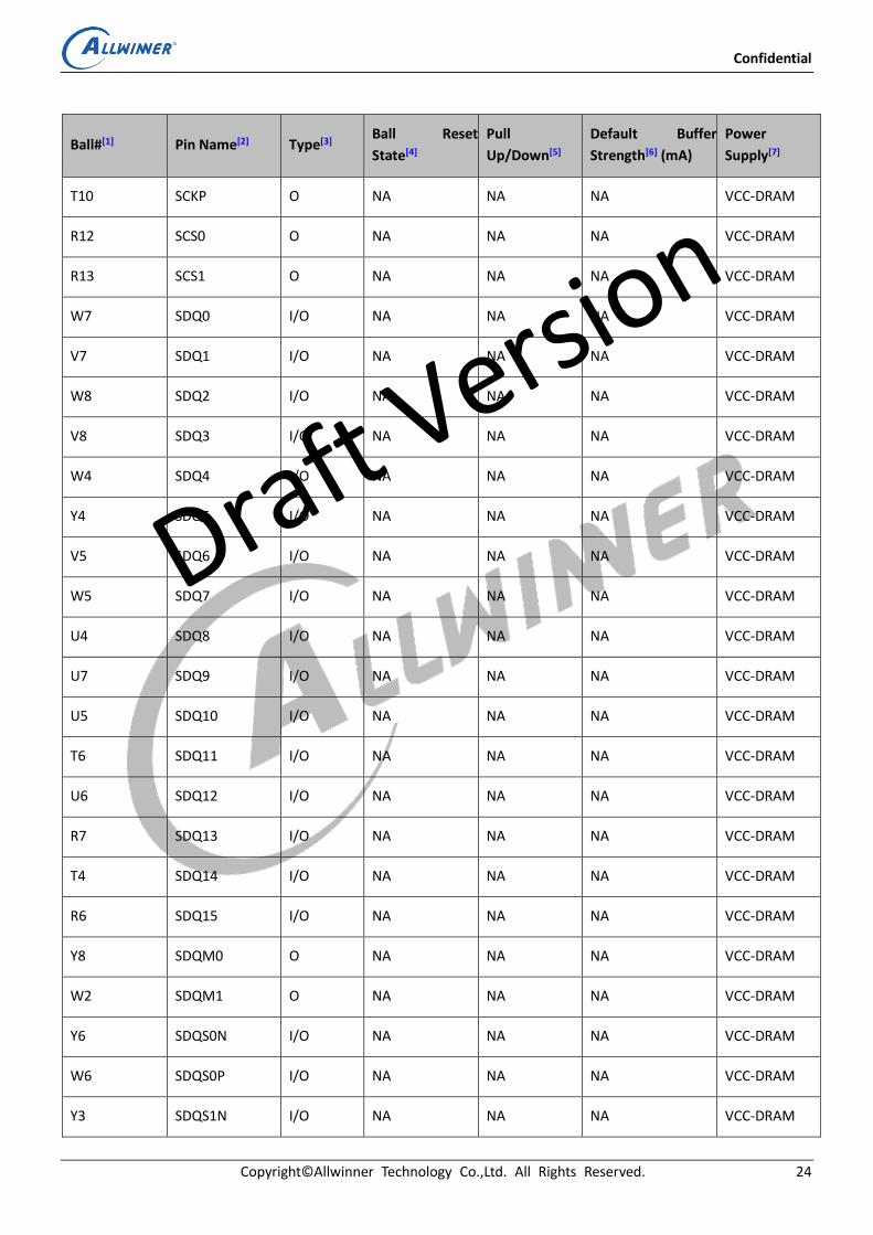
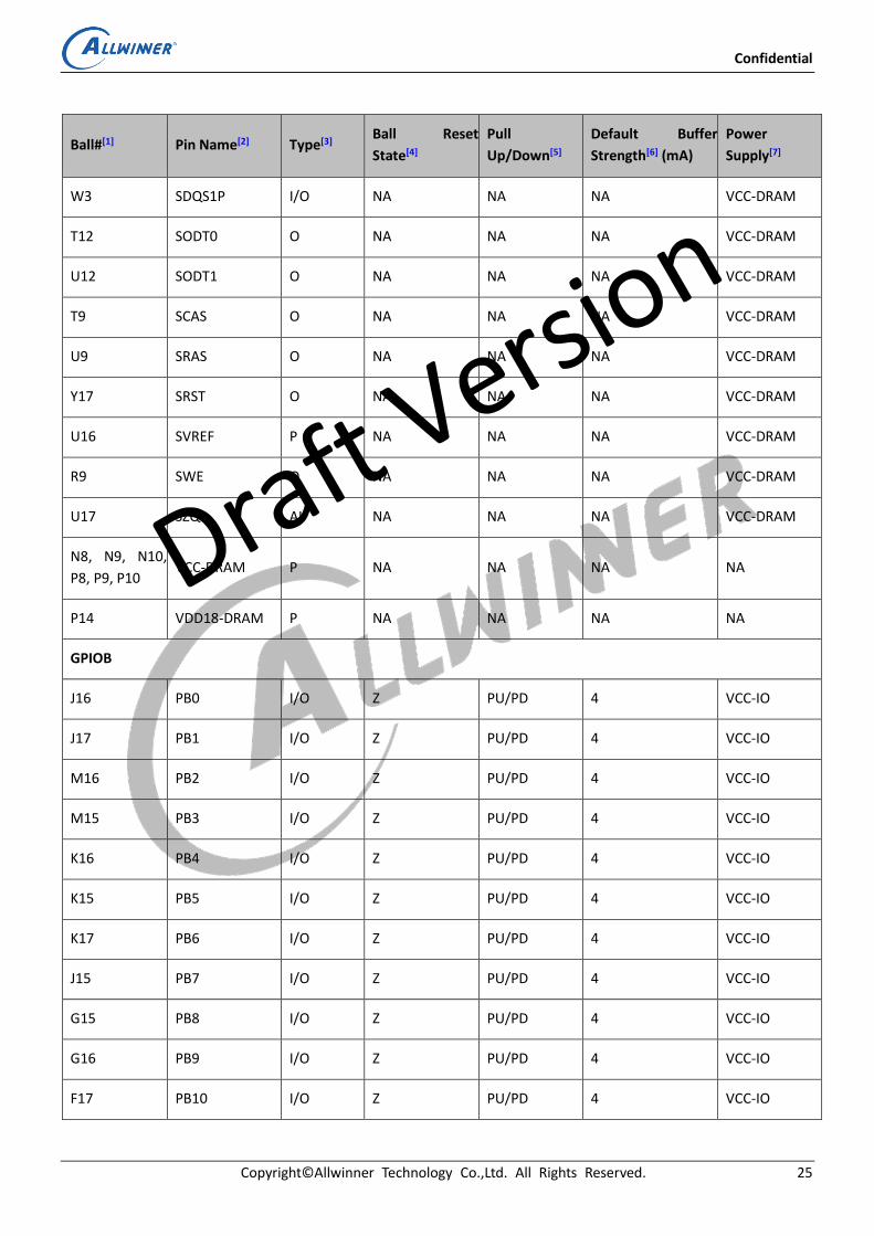
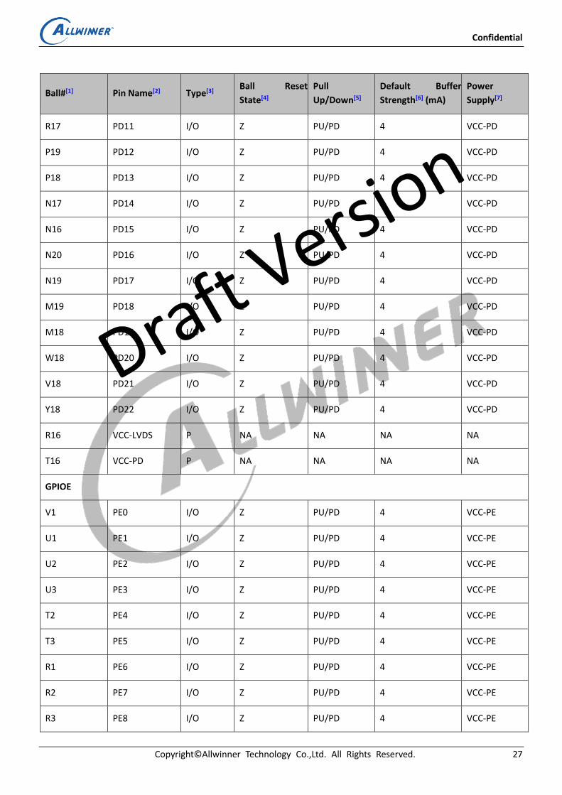
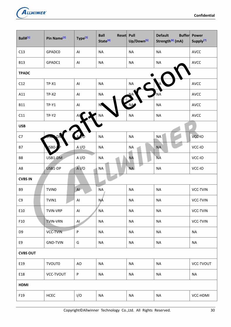
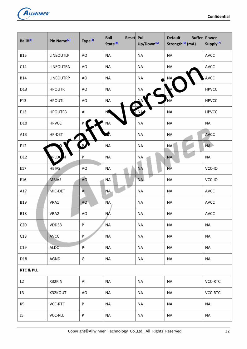
Table 4-2 lists the characteristics of the D1 pins from the following seven aspects.
[1].Ball#: Package ball numbers associated with each signal.
[2].Pin Name: The name of the package pin.
[3].Type: Denotes the signal direction
I (Input),
O (Output),
I/O (Input/Output),
OD (Open-Drain),
A (Analog),
AI (Analog Input),
AO (Analog Output),
P (Power),
G (Ground)
[4].Ball Reset State: The state of the terminal at reset. PU: pull up; PD: pull down; Z: high impedance.
[5].Pull Up/Down: Denotes the presence of an internal pull-up or pull-down resistor. Pull-up and pull-down
resistors can be enabled or disabled via software.
[6].Default Buffer Strength: Defines the default drive strength of the associated output buffer. The maximum
drive strength of each GPIO is 6 mA.
[7].Power Supply: The voltage supply for the IO buffers of the terminal.
Draft Versio
n
Confidential
Copyright© Allwinner Technology Co.,Ltd. All Rights Reserved. 23
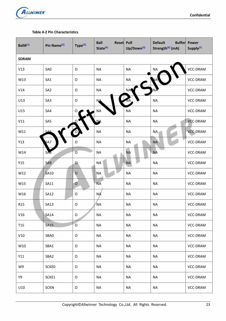
Table 4-2 Pin Characteristics
Ball#[1] Pin Name[2] Type[3] Ball Reset
State[4]
Pull
Up/Down[5]
Default Buffer
Strength[6] (mA)
Power
Supply[7]
SDRAM
V13 SA0 O NA NA NA VCC-DRAM
W13 SA1 O NA NA NA VCC-DRAM
V14 SA2 O NA NA NA VCC-DRAM
U13 SA3 O NA NA NA VCC-DRAM
U15 SA4 O NA NA NA VCC-DRAM
V11 SA5 O NA NA NA VCC-DRAM
W11 SA6 O NA NA NA VCC-DRAM
Y13 SA7 O NA NA NA VCC-DRAM
W14 SA8 O NA NA NA VCC-DRAM
Y15 SA9 O NA NA NA VCC-DRAM
W12 SA10 O NA NA NA VCC-DRAM
W15 SA11 O NA NA NA VCC-DRAM
W16 SA12 O NA NA NA VCC-DRAM
R15 SA13 O NA NA NA VCC-DRAM
V16 SA14 O NA NA NA VCC-DRAM
T15 SA15 O NA NA NA VCC-DRAM
V10 SBA0 O NA NA NA VCC-DRAM
W10 SBA1 O NA NA NA VCC-DRAM
Y11 SBA2 O NA NA NA VCC-DRAM
W9 SCKE0 O NA NA NA VCC-DRAM
Y9 SCKE1 O NA NA NA VCC-DRAM
U10 SCKN O NA NA NA VCC-DRAM
Draft Versio
n
Confidential
Copyright© Allwinner Technology Co.,Ltd. All Rights Reserved. 24
Ball#[1] Pin Name[2] Type[3] Ball Reset
State[4]
Pull
Up/Down[5]
Default Buffer
Strength[6] (mA)
Power
Supply[7]
T10 SCKP O NA NA NA VCC-DRAM
R12 SCS0 O NA NA NA VCC-DRAM
R13 SCS1 O NA NA NA VCC-DRAM
W7 SDQ0 I/O NA NA NA VCC-DRAM
V7 SDQ1 I/O NA NA NA VCC-DRAM
W8 SDQ2 I/O NA NA NA VCC-DRAM
V8 SDQ3 I/O NA NA NA VCC-DRAM
W4 SDQ4 I/O NA NA NA VCC-DRAM
Y4 SDQ5 I/O NA NA NA VCC-DRAM
V5 SDQ6 I/O NA NA NA VCC-DRAM
W5 SDQ7 I/O NA NA NA VCC-DRAM
U4 SDQ8 I/O NA NA NA VCC-DRAM
U7 SDQ9 I/O NA NA NA VCC-DRAM
U5 SDQ10 I/O NA NA NA VCC-DRAM
T6 SDQ11 I/O NA NA NA VCC-DRAM
U6 SDQ12 I/O NA NA NA VCC-DRAM
R7 SDQ13 I/O NA NA NA VCC-DRAM
T4 SDQ14 I/O NA NA NA VCC-DRAM
R6 SDQ15 I/O NA NA NA VCC-DRAM
Y8 SDQM0 O NA NA NA VCC-DRAM
W2 SDQM1 O NA NA NA VCC-DRAM
Y6 SDQS0N I/O NA NA NA VCC-DRAM
W6 SDQS0P I/O NA NA NA VCC-DRAM
Y3 SDQS1N I/O NA NA NA VCC-DRAM
Draft Versio
n
Confidential
Copyright© Allwinner Technology Co.,Ltd. All Rights Reserved. 25
Ball#[1] Pin Name[2] Type[3] Ball Reset
State[4]
Pull
Up/Down[5]
Default Buffer
Strength[6] (mA)
Power
Supply[7]
W3 SDQS1P I/O NA NA NA VCC-DRAM
T12 SODT0 O NA NA NA VCC-DRAM
U12 SODT1 O NA NA NA VCC-DRAM
T9 SCAS O NA NA NA VCC-DRAM
U9 SRAS O NA NA NA VCC-DRAM
Y17 SRST O NA NA NA VCC-DRAM
U16 SVREF P NA NA NA VCC-DRAM
R9 SWE O NA NA NA VCC-DRAM
U17 SZQ AI NA NA NA VCC-DRAM
N8, N9, N10,
P8, P9, P10 VCC-DRAM P NA NA NA NA
P14 VDD18-DRAM P NA NA NA NA
GPIOB
J16 PB0 I/O Z PU/PD 4 VCC-IO
J17 PB1 I/O Z PU/PD 4 VCC-IO
M16 PB2 I/O Z PU/PD 4 VCC-IO
M15 PB3 I/O Z PU/PD 4 VCC-IO
K16 PB4 I/O Z PU/PD 4 VCC-IO
K15 PB5 I/O Z PU/PD 4 VCC-IO
K17 PB6 I/O Z PU/PD 4 VCC-IO
J15 PB7 I/O Z PU/PD 4 VCC-IO
G15 PB8 I/O Z PU/PD 4 VCC-IO
G16 PB9 I/O Z PU/PD 4 VCC-IO
F17 PB10 I/O Z PU/PD 4 VCC-IO
Draft Versio
n

Confidential
Copyright© Allwinner Technology Co.,Ltd. All Rights Reserved. 26
Ball#[1] Pin Name[2] Type[3] Ball Reset
State[4]
Pull
Up/Down[5]
Default Buffer
Strength[6] (mA)
Power
Supply[7]
F15 PB11 I/O Z PU/PD 4 VCC-IO
F16 PB12 I/O Z PU/PD 4 VCC-IO
GPIOC
F2 PC0 I/O Z PU/PD 4 VCC-PC
F1 PC1 I/O Z PU/PD 4 VCC-PC
G3 PC2 I/O Z PU/PD 4 VCC-PC
G2 PC3 I/O PU PU/PD 4 VCC-PC
H3 PC4 I/O PU PU/PD 4 VCC-PC
F5 PC5 I/O PU PU/PD 4 VCC-PC
G6 PC6 I/O Z PU/PD 4 VCC-PC
G5 PC7 I/O Z PU/PD 4 VCC-PC
G4 VCC-PC P NA NA NA NA
GPIOD
W19 PD0 I/O Z PU/PD 4 VCC-PD
V20 PD1 I/O Z PU/PD 4 VCC-PD
V19 PD2 I/O Z PU/PD 4 VCC-PD
U20 PD3 I/O Z PU/PD 4 VCC-PD
U19 PD4 I/O Z PU/PD 4 VCC-PD
U18 PD5 I/O Z PU/PD 4 VCC-PD
T19 PD6 I/O Z PU/PD 4 VCC-PD
T18 PD7 I/O Z PU/PD 4 VCC-PD
R20 PD8 I/O Z PU/PD 4 VCC-PD
R19 PD9 I/O Z PU/PD 4 VCC-PD
T17 PD10 I/O Z PU/PD 4 VCC-PD
Draft Versio
n
Confidential
Copyright© Allwinner Technology Co.,Ltd. All Rights Reserved. 27
Ball#[1] Pin Name[2] Type[3] Ball Reset
State[4]
Pull
Up/Down[5]
Default Buffer
Strength[6] (mA)
Power
Supply[7]
R17 PD11 I/O Z PU/PD 4 VCC-PD
P19 PD12 I/O Z PU/PD 4 VCC-PD
P18 PD13 I/O Z PU/PD 4 VCC-PD
N17 PD14 I/O Z PU/PD 4 VCC-PD
N16 PD15 I/O Z PU/PD 4 VCC-PD
N20 PD16 I/O Z PU/PD 4 VCC-PD
N19 PD17 I/O Z PU/PD 4 VCC-PD
M19 PD18 I/O Z PU/PD 4 VCC-PD
M18 PD19 I/O Z PU/PD 4 VCC-PD
W18 PD20 I/O Z PU/PD 4 VCC-PD
V18 PD21 I/O Z PU/PD 4 VCC-PD
Y18 PD22 I/O Z PU/PD 4 VCC-PD
R16 VCC-LVDS P NA NA NA NA
T16 VCC-PD P NA NA NA NA
GPIOE
V1 PE0 I/O Z PU/PD 4 VCC-PE
U1 PE1 I/O Z PU/PD 4 VCC-PE
U2 PE2 I/O Z PU/PD 4 VCC-PE
U3 PE3 I/O Z PU/PD 4 VCC-PE
T2 PE4 I/O Z PU/PD 4 VCC-PE
T3 PE5 I/O Z PU/PD 4 VCC-PE
R1 PE6 I/O Z PU/PD 4 VCC-PE
R2 PE7 I/O Z PU/PD 4 VCC-PE
R3 PE8 I/O Z PU/PD 4 VCC-PE
Draft Versio
n

Confidential
Copyright© Allwinner Technology Co.,Ltd. All Rights Reserved. 28
Ball#[1] Pin Name[2] Type[3] Ball Reset
State[4]
Pull
Up/Down[5]
Default Buffer
Strength[6] (mA)
Power
Supply[7]
P2 PE9 I/O Z PU/PD 4 VCC-PE
P3 PE10 I/O Z PU/PD 4 VCC-PE
N1 PE11 I/O Z PU/PD 4 VCC-PE
R5 PE12 I/O Z PU/PD 4 VCC-PE
R4 PE13 I/O Z PU/PD 4 VCC-PE
N4 PE14 I/O Z PU/PD 4 VCC-PE
N5 PE15 I/O Z PU/PD 4 VCC-PE
N6 PE16 I/O Z PU/PD 4 VCC-PE
M6 PE17 I/O Z PU/PD 4 VCC-PE
M4 VCC-PE P NA NA NA NA
GPIOF
C2 PF0 I/O Z PU/PD 4 VCC-PF
C1 PF1 I/O Z PU/PD 4 VCC-PF
D2 PF2 I/O Z PU/PD 4 VCC-PF
D1 PF3 I/O Z PU/PD 4 VCC-PF
E3 PF4 I/O Z PU/PD 4 VCC-PF
E2 PF5 I/O Z PU/PD 4 VCC-PF
D3 PF6 I/O Z PU/PD 4 VCC-PF
F4 VCC-PF P NA NA NA NA
GPIOG
B2 PG0 I/O Z PU/PD 4 VCC-PG
B3 PG1 I/O Z PU/PD 4 VCC-PG
A3 PG2 I/O Z PU/PD 4 VCC-PG
C3 PG3 I/O Z PU/PD 4 VCC-PG
Draft Versio
n

Confidential
Copyright© Allwinner Technology Co.,Ltd. All Rights Reserved. 29
Ball#[1] Pin Name[2] Type[3] Ball Reset
State[4]
Pull
Up/Down[5]
Default Buffer
Strength[6] (mA)
Power
Supply[7]
A4 PG4 I/O Z PU/PD 4 VCC-PG
B4 PG5 I/O Z PU/PD 4 VCC-PG
B5 PG6 I/O Z PU/PD 4 VCC-PG
C5 PG7 I/O Z PU/PD 4 VCC-PG
A6 PG8 I/O Z PU/PD 4 VCC-PG
B6 PG9 I/O Z PU/PD 4 VCC-PG
C6 PG10 I/O Z PU/PD 4 VCC-PG
D4 PG11 I/O Z PU/PD 4 VCC-PG
D5 PG12 I/O Z PU/PD 4 VCC-PG
D6 PG13 I/O Z PU/PD 4 VCC-PG
E6 PG14 I/O Z PU/PD 4 VCC-PG
F6 PG15 I/O Z PU/PD 4 VCC-PG
F7 PG16 I/O Z PU/PD 4 VCC-PG
E7 PG17 I/O Z PU/PD 4 VCC-PG
D7 PG18 I/O Z PU/PD 4 VCC-PG
E4 VCC-PG P NA NA NA NA
System
N3 NMI I/O, OD NA NA NA VCC-RTC
N2 TEST I PD PU/PD NA VCC-RTC
A18 FEL I PU PU/PD NA VCC-IO
M2 RESET I, OD NA NA NA VCC-RTC
LRADC
B12 LRADC AI NA NA NA AVCC
GPADC
Draft Versio
n
Confidential
Copyright© Allwinner Technology Co.,Ltd. All Rights Reserved. 30
Ball#[1] Pin Name[2] Type[3] Ball Reset
State[4]
Pull
Up/Down[5]
Default Buffer
Strength[6] (mA)
Power
Supply[7]
C13 GPADC0 AI NA NA NA AVCC
B13 GPADC1 AI NA NA NA AVCC
TPADC
C12 TP-X1 AI NA NA NA AVCC
A11 TP-X2 AI NA NA NA AVCC
B11 TP-Y1 AI NA NA NA AVCC
C11 TP-Y2 AI NA NA NA AVCC
USB
C7 USB0-DM A I/O NA NA NA VCC-IO
B7 USB0-DP A I/O NA NA NA VCC-IO
B8 USB1-DM A I/O NA NA NA VCC-IO
A8 USB1-DP A I/O NA NA NA VCC-IO
CVBS IN
B9 TVIN0 AI NA NA NA VCC-TVIN
C9 TVIN1 AI NA NA NA VCC-TVIN
E10 TVIN-VRP AI NA NA NA VCC-TVIN
F10 TVIN-VRN AI NA NA NA VCC-TVIN
D9 VCC-TVIN P NA NA NA NA
E9 GND-TVIN G NA NA NA NA
CVBS OUT
E19 TVOUT0 AO NA NA NA VCC-TVOUT
E18 VCC-TVOUT P NA NA NA NA
HDMI
F19 HCEC I/O NA NA NA VCC-HDMI
Draft Versio
n

Confidential
Copyright© Allwinner Technology Co.,Ltd. All Rights Reserved. 31
Ball#[1] Pin Name[2] Type[3] Ball Reset
State[4]
Pull
Up/Down[5]
Default Buffer
Strength[6] (mA)
Power
Supply[7]
F20 HHPD I/O NA NA NA VCC-HDMI
G19 HSCL O NA NA NA VCC-HDMI
G18 HSDA I/O NA NA NA VCC-HDMI
K19 HTX0N AO NA NA NA VCC-HDMI
K18 HTX0P AO NA NA NA VCC-HDMI
J19 HTX1N AO NA NA NA VCC-HDMI
J18 HTX1P AO NA NA NA VCC-HDMI
H20 HTX2N AO NA NA NA VCC-HDMI
H19 HTX2P AO NA NA NA VCC-HDMI
L20 HTXCN AO NA NA NA VCC-HDMI
L19 HTXCP AO NA NA NA VCC-HDMI
M17 VCC-HDMI P NA NA NA NA
Audio Codec
D20 MICIN1P AI NA NA NA AVCC
D19 MICIN1N AI NA NA NA AVCC
E15 MICIN2P AI NA NA NA AVCC
D15 MICIN2N AI NA NA NA AVCC
D17 MICIN3P AI NA NA NA AVCC
D16 MICIN3N AI NA NA NA AVCC
C17 FMINR AI NA NA NA AVCC
B17 FMINL AI NA NA NA AVCC
C16 LINEINR AI NA NA NA AVCC
B16 LINEINL AI NA NA NA AVCC
C15 LINEOUTLN AO NA NA NA AVCC
Draft Versio
n
Confidential
Copyright© Allwinner Technology Co.,Ltd. All Rights Reserved. 32
Ball#[1] Pin Name[2] Type[3] Ball Reset
State[4]
Pull
Up/Down[5]
Default Buffer
Strength[6] (mA)
Power
Supply[7]
B15 LINEOUTLP AO NA NA NA AVCC
C14 LINEOUTRN AO NA NA NA AVCC
B14 LINEOUTRP AO NA NA NA AVCC
D13 HPOUTR AO NA NA NA HPVCC
F13 HPOUTL AO NA NA NA HPVCC
E13 HPOUTFB AI NA NA NA HPVCC
D10 HPVCC P NA NA NA NA
A13 HP-DET AI NA NA NA AVCC
E12 HPLDO P NA NA NA NA
D12 HPLDOIN P NA NA NA NA
E17 HBIAS AO NA NA NA VCC-IO
E16 MBIAS AO NA NA NA VCC-IO
A17 MIC-DET AI NA NA NA AVCC
B19 VRA1 AO NA NA NA AVCC
B18 VRA2 AO NA NA NA AVCC
C20 VDD33 P NA NA NA NA
C18 AVCC P NA NA NA NA
C19 ALDO P NA NA NA NA
D18 AGND G NA NA NA NA
RTC & PLL
L2 X32KIN AI NA NA NA VCC-RTC
L3 X32KOUT AO NA NA NA VCC-RTC
K5 VCC-RTC P NA NA NA NA
J5 VCC-PLL P NA NA NA NA
Draft Versio
n

Confidential
Copyright© Allwinner Technology Co.,Ltd. All Rights Reserved. 33
Ball#[1] Pin Name[2] Type[3] Ball Reset
State[4]
Pull
Up/Down[5]
Default Buffer
Strength[6] (mA)
Power
Supply[7]
DCXO
K1 DXIN AI NA NA NA VCC-DCXO
K2 DXOUT AO NA NA NA VCC-DCXO
J2 REFCLK-OUT AO NA NA NA VCC-DCXO
K4 VCC-DCXO P NA NA NA NA
Power
M7 LDO-IN P NA NA NA NA
L7 LDOA-OUT P NA NA NA NA
N7 LDOB-OUT P NA NA NA NA
G17 VCC-IO P NA NA NA NA
J4 VCC-EFUSE P NA NA NA NA
G13, G14, H13,
H14, J13, J14 VDD-SYS P NA NA NA NA
G7, G8, H7, H8,
H9 VDD-CPU P NA NA NA NA
G9 VDD-CPUFB P NA NA NA NA
GND
A1, A15, A19,
A2, A20, B1,
B10, B20, C10,
C4, C8, E5, F12,
F18, F3, F9,
G10, G11, G12,
H1, H10, H11,
H12, H18, H2,
J10, J11, J12,
J3, J6, J7, J8,
J9, K10, K11,
K12, K13, K14,
K3, K6, K7, K8,
K9, L10, L11,
GND G NA NA NA NA
Draft Versio
n
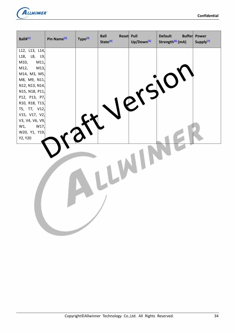
Confidential
Copyright© Allwinner Technology Co.,Ltd. All Rights Reserved. 34
Ball#[1] Pin Name[2] Type[3] Ball Reset
State[4]
Pull
Up/Down[5]
Default Buffer
Strength[6] (mA)
Power
Supply[7]
L12, L13, L14,
L18, L8, L9,
M10, M11,
M12, M13,
M14, M3, M5,
M8, M9, N11,
N12, N13, N14,
N15, N18, P11,
P12, P13, P7,
R10, R18, T13,
T5, T7, V12,
V15, V17, V2,
V3, V4, V6, V9,
W1, W17,
W20, Y1, Y19,
Y2, Y20
Draft Versio
n

Confidential
Copyright© Allwinner Technology Co.,Ltd. All Rights Reserved. 35
4.3 GPIO Multiplex Function
The following table provides a description of the D1 GPIO multiplex function.
NOTE
For each GPIO, Function0 is input function; Function1 is output function; Function9 to Function13 are reserved.
Table 4-3 GPIO Multiplex Function
Pin
Name
GPIO
Group
IO
Type Function2 Function3 Function4 Function5 Function6 Function7 Function8 Function14
PB0
GPIOB
I/O PWM3 IR-TX TWI2-SCK SPI1-WP/
DBI-TE UART0-TX UART2-TX OWA-OUT PB-EINT0
PB1 I/O PWM4 I2S2-DOUT3 TWI2-SDA I2S2-DIN3 UART0-RX UART2-RX IR-RX PB-EINT1
PB2 I/O LCD0-D0 I2S2-DOUT2 TWI0-SDA I2S2-DIN2 LCD0-D18 UART4-TX PB-EINT2
PB3 I/O LCD0-D1 I2S2-DOUT1 TWI0-SCK I2S2-DIN0 LCD0-D19 UART4-RX PB-EINT3
PB4 I/O LCD0-D8 I2S2-DOUT0 TWI1-SCK I2S2-DIN1 LCD0-D20 UART5-TX PB-EINT4
PB5 I/O LCD0-D9 I2S2-BCLK TWI1-SDA PWM0 LCD0-D21 UART5-RX PB-EINT5
PB6 I/O LCD0-D16 I2S2-LRCK TWI3-SCK PWM1 LCD0-D22 UART3-TX CPUBIST0 PB-EINT6
PB7 I/O LCD0-D17 I2S2-MCLK TWI3-SDA IR-RX LCD0-D23 UART3-RX CPUBIST1 PB-EINT7
PB8 I/O DMIC-DATA3 PWM5 TWI2-SCK
SPI1-HOLD/
DBI-DCX/
DBI-WRX
UART0-TX UART1-TX PB-EINT8
PB9 I/O DMIC-DATA2 PWM6 TWI2-SDA
SPI1-MISO/
DBI-SDI/
DBI-TE/
DBI-DCX
UART0-RX UART1-RX PB-EINT9
PB10 I/O DMIC-DATA1 PWM7 TWI0-SCK SPI1-MOSI/
DBI-SDO CLK-FANOUT0 UART1-RTS PB-EINT10
PB11 I/O DMIC-DATA0 PWM2 TWI0-SDA SPI1-CLK/
DBI-SCLK CLK-FANOUT1 UART1-CTS PB-EINT11
PB12 I/O DMIC-CLK PWM0 OWA-IN SPI1-CS/
DBI-CSX CLK-FANOUT2 IR-RX PB-EINT12
PC0
GPIOC
I/O UART2-TX TWI2-SCK LEDC-DO PC-EINT0
PC1 I/O UART2-RX TWI2-SDA PC-EINT1
PC2 I/O SPI0-CLK SDC2-CLK PC-EINT2
PC3 I/O SPI0-CS0 SDC2-CMD PC-EINT3
PC4 I/O SPI0-MOSI SDC2-D2 BOOT-SEL0 PC-EINT4
PC5 I/O SPI0-MISO SDC2-D1 BOOT-SEL1 PC-EINT5
PC6 I/O SPI0-WP SDC2-D0 UART3-TX TWI3-SCK DBG-CLK PC-EINT6
PC7 I/O SPI0-HOLD SDC2-D3 UART3-RX TWI3-SDA TCON-TRIG PC-EINT7
PD0
GPIOD
I/O LCD0-D2 LVDS0-V0P DSI-D0P TWI0-SCK PD-EINT0
PD1 I/O LCD0-D3 LVDS0-V0N DSI-D0N UART2-TX PD-EINT1
Draft Versio
n
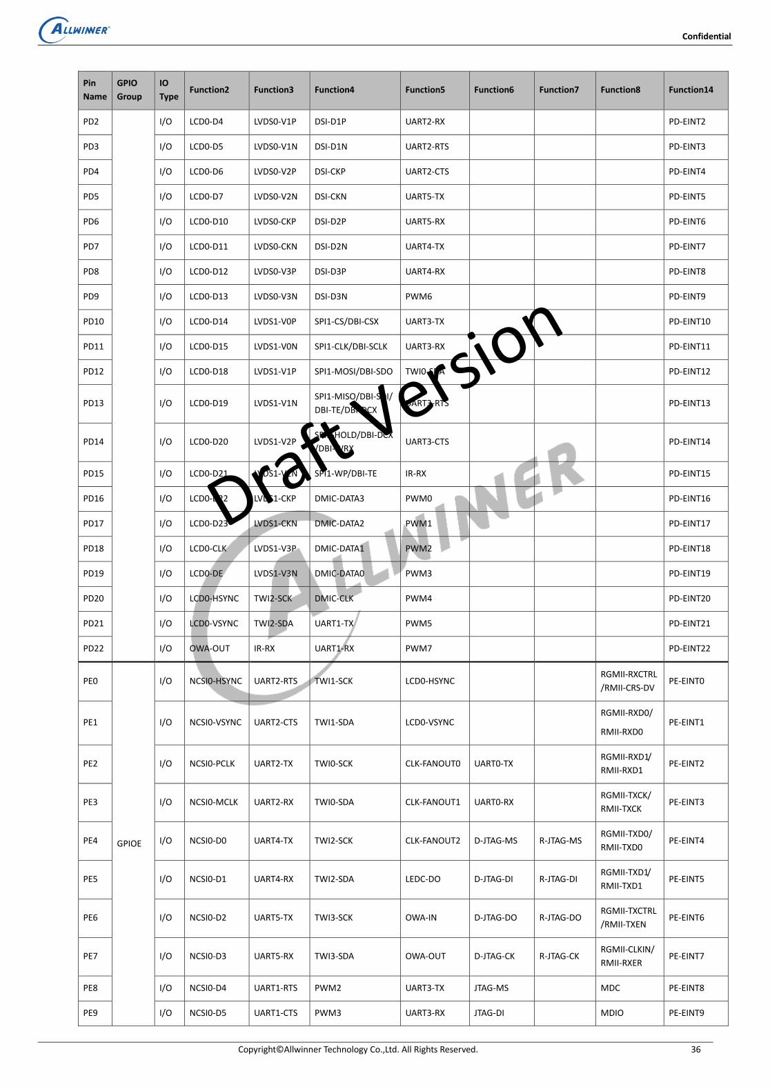
Confidential
Copyright© Allwinner Technology Co.,Ltd. All Rights Reserved. 36
Pin
Name
GPIO
Group
IO
Type Function2 Function3 Function4 Function5 Function6 Function7 Function8 Function14
PD2 I/O LCD0-D4 LVDS0-V1P DSI-D1P UART2-RX PD-EINT2
PD3 I/O LCD0-D5 LVDS0-V1N DSI-D1N UART2-RTS PD-EINT3
PD4 I/O LCD0-D6 LVDS0-V2P DSI-CKP UART2-CTS PD-EINT4
PD5 I/O LCD0-D7 LVDS0-V2N DSI-CKN UART5-TX PD-EINT5
PD6 I/O LCD0-D10 LVDS0-CKP DSI-D2P UART5-RX PD-EINT6
PD7 I/O LCD0-D11 LVDS0-CKN DSI-D2N UART4-TX PD-EINT7
PD8 I/O LCD0-D12 LVDS0-V3P DSI-D3P UART4-RX PD-EINT8
PD9 I/O LCD0-D13 LVDS0-V3N DSI-D3N PWM6 PD-EINT9
PD10 I/O LCD0-D14 LVDS1-V0P SPI1-CS/DBI-CSX UART3-TX PD-EINT10
PD11 I/O LCD0-D15 LVDS1-V0N SPI1-CLK/DBI-SCLK UART3-RX PD-EINT11
PD12 I/O LCD0-D18 LVDS1-V1P SPI1-MOSI/DBI-SDO TWI0-SDA PD-EINT12
PD13 I/O LCD0-D19 LVDS1-V1N SPI1-MISO/DBI-SDI/
DBI-TE/DBI-DCX UART3-RTS PD-EINT13
PD14 I/O LCD0-D20 LVDS1-V2P SPI1-HOLD/DBI-DCX
/DBI-WRX UART3-CTS PD-EINT14
PD15 I/O LCD0-D21 LVDS1-V2N SPI1-WP/DBI-TE IR-RX PD-EINT15
PD16 I/O LCD0-D22 LVDS1-CKP DMIC-DATA3 PWM0 PD-EINT16
PD17 I/O LCD0-D23 LVDS1-CKN DMIC-DATA2 PWM1 PD-EINT17
PD18 I/O LCD0-CLK LVDS1-V3P DMIC-DATA1 PWM2 PD-EINT18
PD19 I/O LCD0-DE LVDS1-V3N DMIC-DATA0 PWM3 PD-EINT19
PD20 I/O LCD0-HSYNC TWI2-SCK DMIC-CLK PWM4 PD-EINT20
PD21 I/O LCD0-VSYNC TWI2-SDA UART1-TX PWM5 PD-EINT21
PD22 I/O OWA-OUT IR-RX UART1-RX PWM7 PD-EINT22
PE0
GPIOE
I/O NCSI0-HSYNC UART2-RTS TWI1-SCK LCD0-HSYNC RGMII-RXCTRL
/RMII-CRS-DV PE-EINT0
PE1 I/O NCSI0-VSYNC UART2-CTS TWI1-SDA LCD0-VSYNC RGMII-RXD0/
RMII-RXD0 PE-EINT1
PE2 I/O NCSI0-PCLK UART2-TX TWI0-SCK CLK-FANOUT0 UART0-TX RGMII-RXD1/
RMII-RXD1 PE-EINT2
PE3 I/O NCSI0-MCLK UART2-RX TWI0-SDA CLK-FANOUT1 UART0-RX RGMII-TXCK/
RMII-TXCK PE-EINT3
PE4 I/O NCSI0-D0 UART4-TX TWI2-SCK CLK-FANOUT2 D-JTAG-MS R-JTAG-MS RGMII-TXD0/
RMII-TXD0 PE-EINT4
PE5 I/O NCSI0-D1 UART4-RX TWI2-SDA LEDC-DO D-JTAG-DI R-JTAG-DI RGMII-TXD1/
RMII-TXD1 PE-EINT5
PE6 I/O NCSI0-D2 UART5-TX TWI3-SCK OWA-IN D-JTAG-DO R-JTAG-DO RGMII-TXCTRL
/RMII-TXEN PE-EINT6
PE7 I/O NCSI0-D3 UART5-RX TWI3-SDA OWA-OUT D-JTAG-CK R-JTAG-CK RGMII-CLKIN/
RMII-RXER PE-EINT7
PE8 I/O NCSI0-D4 UART1-RTS PWM2 UART3-TX JTAG-MS MDC PE-EINT8
PE9 I/O NCSI0-D5 UART1-CTS PWM3 UART3-RX JTAG-DI MDIO PE-EINT9
Draft Versio
n
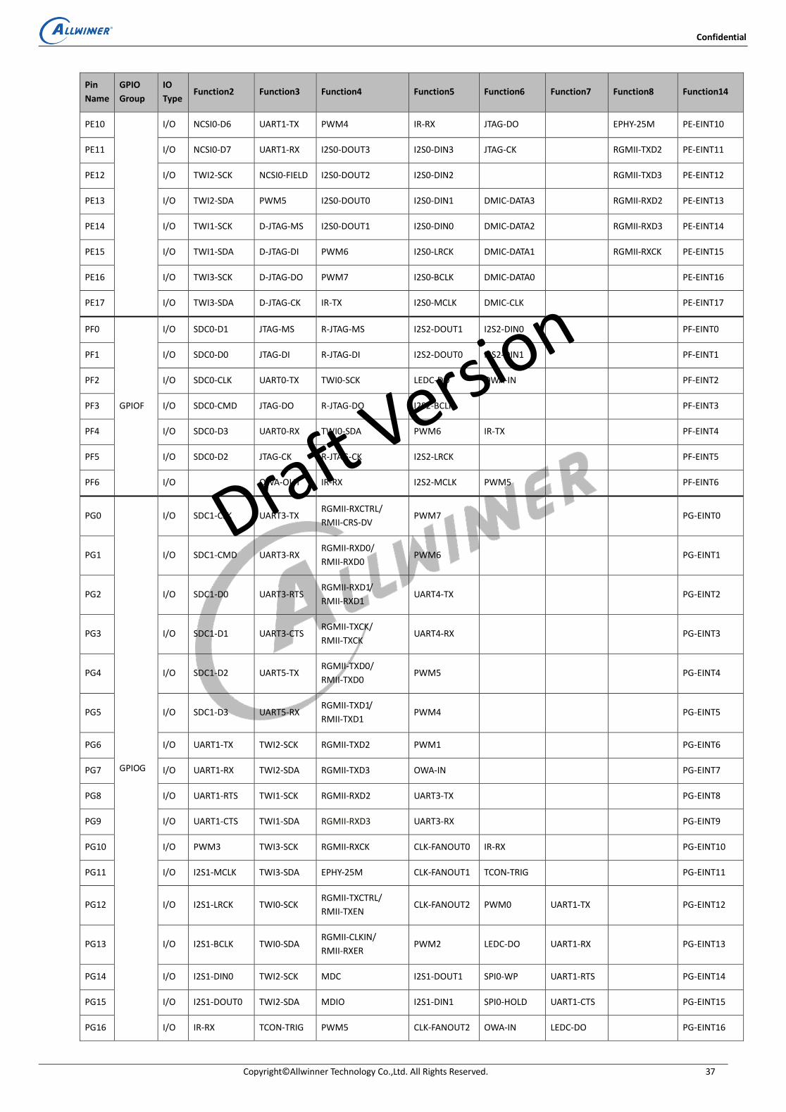
Confidential
Copyright© Allwinner Technology Co.,Ltd. All Rights Reserved. 37
Pin
Name
GPIO
Group
IO
Type Function2 Function3 Function4 Function5 Function6 Function7 Function8 Function14
PE10 I/O NCSI0-D6 UART1-TX PWM4 IR-RX JTAG-DO EPHY-25M PE-EINT10
PE11 I/O NCSI0-D7 UART1-RX I2S0-DOUT3 I2S0-DIN3 JTAG-CK RGMII-TXD2 PE-EINT11
PE12 I/O TWI2-SCK NCSI0-FIELD I2S0-DOUT2 I2S0-DIN2 RGMII-TXD3 PE-EINT12
PE13 I/O TWI2-SDA PWM5 I2S0-DOUT0 I2S0-DIN1 DMIC-DATA3 RGMII-RXD2 PE-EINT13
PE14 I/O TWI1-SCK D-JTAG-MS I2S0-DOUT1 I2S0-DIN0 DMIC-DATA2 RGMII-RXD3 PE-EINT14
PE15 I/O TWI1-SDA D-JTAG-DI PWM6 I2S0-LRCK DMIC-DATA1 RGMII-RXCK PE-EINT15
PE16 I/O TWI3-SCK D-JTAG-DO PWM7 I2S0-BCLK DMIC-DATA0 PE-EINT16
PE17 I/O TWI3-SDA D-JTAG-CK IR-TX I2S0-MCLK DMIC-CLK PE-EINT17
PF0
GPIOF
I/O SDC0-D1 JTAG-MS R-JTAG-MS I2S2-DOUT1 I2S2-DIN0 PF-EINT0
PF1 I/O SDC0-D0 JTAG-DI R-JTAG-DI I2S2-DOUT0 I2S2-DIN1 PF-EINT1
PF2 I/O SDC0-CLK UART0-TX TWI0-SCK LEDC-DO OWA-IN PF-EINT2
PF3 I/O SDC0-CMD JTAG-DO R-JTAG-DO I2S2-BCLK PF-EINT3
PF4 I/O SDC0-D3 UART0-RX TWI0-SDA PWM6 IR-TX PF-EINT4
PF5 I/O SDC0-D2 JTAG-CK R-JTAG-CK I2S2-LRCK PF-EINT5
PF6 I/O OWA-OUT IR-RX I2S2-MCLK PWM5 PF-EINT6
PG0
GPIOG
I/O SDC1-CLK UART3-TX RGMII-RXCTRL/
RMII-CRS-DV PWM7 PG-EINT0
PG1 I/O SDC1-CMD UART3-RX RGMII-RXD0/
RMII-RXD0 PWM6 PG-EINT1
PG2 I/O SDC1-D0 UART3-RTS RGMII-RXD1/
RMII-RXD1 UART4-TX PG-EINT2
PG3 I/O SDC1-D1 UART3-CTS RGMII-TXCK/
RMII-TXCK UART4-RX PG-EINT3
PG4 I/O SDC1-D2 UART5-TX RGMII-TXD0/
RMII-TXD0 PWM5 PG-EINT4
PG5 I/O SDC1-D3 UART5-RX RGMII-TXD1/
RMII-TXD1 PWM4 PG-EINT5
PG6 I/O UART1-TX TWI2-SCK RGMII-TXD2 PWM1 PG-EINT6
PG7 I/O UART1-RX TWI2-SDA RGMII-TXD3 OWA-IN PG-EINT7
PG8 I/O UART1-RTS TWI1-SCK RGMII-RXD2 UART3-TX PG-EINT8
PG9 I/O UART1-CTS TWI1-SDA RGMII-RXD3 UART3-RX PG-EINT9
PG10 I/O PWM3 TWI3-SCK RGMII-RXCK CLK-FANOUT0 IR-RX PG-EINT10
PG11 I/O I2S1-MCLK TWI3-SDA EPHY-25M CLK-FANOUT1 TCON-TRIG PG-EINT11
PG12 I/O I2S1-LRCK TWI0-SCK RGMII-TXCTRL/
RMII-TXEN CLK-FANOUT2 PWM0 UART1-TX PG-EINT12
PG13 I/O I2S1-BCLK TWI0-SDA RGMII-CLKIN/
RMII-RXER PWM2 LEDC-DO UART1-RX PG-EINT13
PG14 I/O I2S1-DIN0 TWI2-SCK MDC I2S1-DOUT1 SPI0-WP UART1-RTS PG-EINT14
PG15 I/O I2S1-DOUT0 TWI2-SDA MDIO I2S1-DIN1 SPI0-HOLD UART1-CTS PG-EINT15
PG16 I/O IR-RX TCON-TRIG PWM5 CLK-FANOUT2 OWA-IN LEDC-DO PG-EINT16
Draft Versio
n

Confidential
Copyright© Allwinner Technology Co.,Ltd. All Rights Reserved. 38
Pin
Name
GPIO
Group
IO
Type Function2 Function3 Function4 Function5 Function6 Function7 Function8 Function14
PG17 I/O UART2-TX TWI3-SCK PWM7 CLK-FANOUT0 IR-TX UART0-TX PG-EINT17
PG18 I/O UART2-RX TWI3-SDA PWM6 CLK-FANOUT1 OWA-OUT UART0-RX PG-EINT18
Draft Versio
n

Confidential
Copyright© Allwinner Technology Co.,Ltd. All Rights Reserved. 39
4.4 Detailed Signal Description
Table 4-4 shows the detailed function description of every signal based on the different interface.
[1].Signal Name: The name of every signal.
[2].Description: The detailed function description of every signal.
[3].Type: Denotes the signal direction:
I (Input),
O (Output),
I/O (Input/Output),
OD (Open-Drain),
A (Analog),
AI (Analog Input),
AO (Analog Output),
A I/O (Analog Input/Output),
P (Power),
G (Ground)
Table 4-4 Detailed Signal Description
Signal Name[1] Description[2] Type[3]
DRAM
SA[15:0] DRAM Address Signal to the Memory Device O
SBA[2:0] DRAM Bank Address Signal to the Memory Device O
SCKE[1:0] DRAM Clock Enable Signal to the Memory Device O
SCKN DRAM Active-Low Clock Signal to the Memory Device O
SCKP DRAM Active-High Clock Signal to the Memory Device O
SCS[1:0] DRAM Chip Select Signal to the Memory Device O
SDQ[15:0] DRAM Bidirectional Data line to the Memory Device I/O
SDQM[1:0] DRAM Data Mask Signal to the Memory Device O
SDQS[1:0]N DRAM Active-Low Bidirectional Data Strobes to the
Memory Device I/O
Draft Versio
n

Confidential
Copyright© Allwinner Technology Co.,Ltd. All Rights Reserved. 40
Signal Name[1] Description[2] Type[3]
SDQS[1:0]P DRAM Active-High Bidirectional Data Strobes to the
Memory Device I/O
SODT[1:0] DRAM On-Die Termination Output Signal O
SCAS DRAM Column Address Strobe O
SRAS DRAM Row Address Strobe O
SRST DRAM Reset Signal to the Memory Device O
SVREF DRAM Reference Voltage P
SWE DRAM Write Enable O
SZQ DRAM External Reference Resistor for Impedance
Calibration AI
VCC-DRAM DRAM Power Supply P
VDD18-DRAM Power Supply for DRAM Controller P
System Control
BOOT-SEL[1:0] Boot Media Select I
RESET Reset Signal (low active) I, OD
NMI Non-maskable Interrupt I/O, OD
TEST Test Signal I
FEL
Boot Select
Jump to the Try Media Boot process when FEL is high
level, or else enter into the mandatory upgrade
process.
For more details, see section 3.4 “BROM System” in the
D1_User_Manual.
I
Clock
X32KIN Clock Input of 32.768 kHz Crystal AI
X32KOUT Clock Output of 32.768 kHz Crystal AO
VCC-RTC RTC Power P
Draft Versio
n

Confidential
Copyright© Allwinner Technology Co.,Ltd. All Rights Reserved. 41
Signal Name[1] Description[2] Type[3]
VCC-PLL PLL Power Supply P
DCXO
REFCLK-OUT Digital Compensated Crystal Oscillator Clock Fanout AO
DXIN Digital Compensated Crystal Oscillator Input AI
DXOUT Digital Compensated Crystal Oscillator Output AO
VCC-DCXO Digital Compensated Crystal Oscillator Power P
USB
USB0-DM USB DRD Data Signal DM A I/O
USB0-DP USB DRD Data Signal DP A I/O
USB1-DM USB HOST Data Signal DM A I/O
USB1-DP USB HOST Data Signal DP A I/O
GPADC
GPADC0 General Purpose ADC Input Channel 0 AI
GPADC1 General Purpose ADC Input Channel 1 AI
TPADC
TP-X1 Touch Panel X1 Input AI
TP-X2 Touch Panel X2 Input AI
TP-Y1 Touch Panel Y1 Input AI
TP-Y2 Touch Panel Y2 Input AI
LRADC
LRADC Low Rate ADC AI
HDMI
HCEC HDMI Consumer Electronics Control I/O
HHPD HDMI Hot Plug Detection Signal I/O
Draft Versio
n
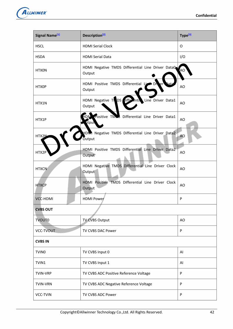
Confidential
Copyright© Allwinner Technology Co.,Ltd. All Rights Reserved. 42
Signal Name[1] Description[2] Type[3]
HSCL HDMI Serial Clock O
HSDA HDMI Serial Data I/O
HTX0N HDMI Negative TMDS Differential Line Driver Data0
Output AO
HTX0P HDMI Positive TMDS Differential Line Driver Data0
Output AO
HTX1N HDMI Negative TMDS Differential Line Driver Data1
Output AO
HTX1P HDMI Positive TMDS Differential Line Driver Data1
Output AO
HTX2N HDMI Negative TMDS Differential Line Driver Data2
Output AO
HTX2P HDMI Positive TMDS Differential Line Driver Data2
Output AO
HTXCN HDMI Negative TMDS Differential Line Driver Clock
Output AO
HTXCP HDMI Positive TMDS Differential Line Driver Clock
Output AO
VCC-HDMI HDMI Power P
CVBS OUT
TVOUT0 TV CVBS Output AO
VCC-TVOUT TV CVBS DAC Power P
CVBS IN
TVIN0 TV CVBS Input 0 AI
TVIN1 TV CVBS Input 1 AI
TVIN-VRP TV CVBS ADC Positive Reference Voltage P
TVIN-VRN TV CVBS ADC Negative Reference Voltage P
VCC-TVIN TV CVBS ADC Power P
Draft Versio
n

Confidential
Copyright© Allwinner Technology Co.,Ltd. All Rights Reserved. 43
Signal Name[1] Description[2] Type[3]
AUDIO CODEC
LINEOUTLN Lineout Left Channel Negative Differential Output AO
LINEOUTLP Lineout Left Channel Positive Differential Output AO
LINEOUTRN Lineout Right Channel Negative Differential Output AO
LINEOUTRP Lineout Right Channel Positive Differential Output AO
HPOUTR Headphone Right Output AO
HPOUTL Headphone Light Output AO
HPOUTFB Pseudo Differential Headphone Ground Reference AI
HPVCC Headphone Power 1.8 V P
MICIN1P Microphone Differential Positive Input 1 AI
MICIN1N Microphone Differential Negative Input 1 AI
MICIN2P Microphone Differential Positive Input 2 AI
MICIN2N Microphone Differential Negative Input 2 AI
MICIN3P Microphone Differential Positive Input 3 AI
MICIN3N Microphone Differential Negative Input 3 AI
FMINR FMIN Right Input AI
FMINL FMIN Left Input AI
LINEINR LINEIN Right Single-End Input AI
LINEINL LINEIN Left Single-End Input AI
HP-DET Headphone Jack Detect AI
HPLDO Headphone LDO 1.8 V (bonding with HPVCC) P
HPLDOIN Headphone LDO Input 3.3 V P
VDD33 Analog Power 3.3 V P
ALDO Analog Power 1.8 V (bonding with AVCC) P
Draft Versio
n

Confidential
Copyright© Allwinner Technology Co.,Ltd. All Rights Reserved. 44
Signal Name[1] Description[2] Type[3]
HBIAS Second Bias Voltage Output for Headset Microphone AO
MBIAS First Bias Voltage Output for Main Microphone AO
MIC-DET Headphone MIC Detect AI
VRA1 Internal Reference Voltage AO
VRA2 Internal Reference Voltage AO
AVCC Power Supply for Analog Part P
AGND Analog Ground G
LCD
LCD0-D[23:0] LCD Data Output O
LCD0-CLK LCD Clock
The pixel data are synchronized by this clock O
LCD0-VSYNC LCD Vertical Sync
It indicates one new frame O
LCD0-HSYNC LCD Horizontal Sync
It indicates one new scan line O
LCD0-DE LCD Data Output Enable O
TCON-TRIG LCD Sync (TCON outputs to LCD for sync) O
LVDS
LVDS0-CKP LVDS0 Positive Port of Clock O
LVDS0-CKN LVDS0 Negative Port of Clock O
LVDS0-V[3:0]P LVDS0 Positive Port of Data Channel [3:0] O
LVDS0-V[3:0]N LVDS0 Negative Port of Data Channel [3:0] O
LVDS1-CKP LVDS1 Positive Port of Clock O
LVDS1-CKN LVDS1 Negative Port of Clock O
LVDS1-V[3:0]P LVDS1 Positive Port of Data Channel [3:0] O
Draft Versio
n

Confidential
Copyright© Allwinner Technology Co.,Ltd. All Rights Reserved. 45
Signal Name[1] Description[2] Type[3]
LVDS1-V[3:0]N LVDS1 Negative Port of Data Channel [3:0] O
DSI
DSI-D[3:0]P DSI Differential Data [3:0] Positive Signal O
DSI-D[3:0]N DSI Differential Data [3:0] Negative Signal O
DSI-CKP DSI Differential Clock Positive Signal O
DSI-CKN DSI Differential Clock Negative Signal O
Parallel CSI
NCSI0-PCLK Parallel CSI Pixel Clock I
NCSI0-MCLK Parallel CSI Master Clock O
NCSI0-HSYNC Parallel CSI Horizontal Synchronous I
NCSI0-VSYNC Parallel CSI Vertical Synchronous I
NCSI0-D[7:0] Parallel CSI Data Bit I
NCSI0-FIELD Parallel CSI Field Index I
SMHC
SDC0-CMD Command Signal for SD Card I/O, OD
SDC0-CLK Clock for SD Card O
SDC0-D[3:0] Data Input and Output for SD Card I/O
SDC1-CMD Command Signal for SDIO WIFI I/O, OD
SDC1-CLK Clock for SDIO WIFI O
SDC1-D[3:0] Data Input and Output for SDIO WIFI I/O
SDC2-CMD Command Signal for eMMC I/O, OD
SDC2-CLK Clock for eMMC O
SDC2-D[3:0] Data Input and Output for eMMC I/O
I2S/PCM
Draft Versio
n
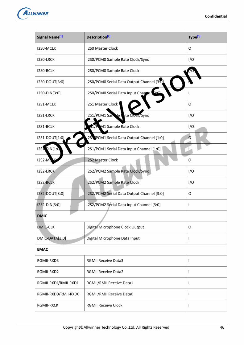
Confidential
Copyright© Allwinner Technology Co.,Ltd. All Rights Reserved. 46
Signal Name[1] Description[2] Type[3]
I2S0-MCLK I2S0 Master Clock O
I2S0-LRCK I2S0/PCM0 Sample Rate Clock/Sync I/O
I2S0-BCLK I2S0/PCM0 Sample Rate Clock I/O
I2S0-DOUT[3:0] I2S0/PCM0 Serial Data Output Channel [3:0] O
I2S0-DIN[3:0] I2S0/PCM0 Serial Data Input Channel [3:0] I
I2S1-MCLK I2S1 Master Clock O
I2S1-LRCK I2S1/PCM1 Sample Rate Clock/Sync I/O
I2S1-BCLK I2S1/PCM1 Sample Rate Clock I/O
I2S1-DOUT[1:0] I2S1/PCM1 Serial Data Output Channel [1:0] O
I2S1-DIN[1:0] I2S1/PCM1 Serial Data Input Channel [1:0] I
I2S2-MCLK I2S2 Master Clock O
I2S2-LRCK I2S2/PCM2 Sample Rate Clock/Sync I/O
I2S2-BCLK I2S2/PCM2 Sample Rate Clock I/O
I2S2-DOUT[3:0] I2S2/PCM2 Serial Data Output Channel [3:0] O
I2S2-DIN[3:0] I2S2/PCM2 Serial Data Input Channel [3:0] I
DMIC
DMIC-CLK Digital Microphone Clock Output O
DMIC-DATA[3:0] Digital Microphone Data Input I
EMAC
RGMII-RXD3 RGMII Receive Data3 I
RGMII-RXD2 RGMII Receive Data2 I
RGMII-RXD1/RMII-RXD1 RGMII/RMII Receive Data1 I
RGMII-RXD0/RMII-RXD0 RGMII/RMII Receive Data0 I
RGMII-RXCK RGMII Receive Clock I
Draft Versio
n

Confidential
Copyright© Allwinner Technology Co.,Ltd. All Rights Reserved. 47
Signal Name[1] Description[2] Type[3]
RGMII-RXCTRL/
RMII-CRS-DV
RGMII Receive Control/RMII Carrier Sense Receive Data
Valid I
RGMII-CLKIN/RMII-RXER RGMII Transmit Clock from External/RMII Receive Error I
RGMII-TXD3 RGMII Transmit Data3 O
RGMII-TXD2 RGMII Transmit Data2 O
RGMII-TXD1/RMII-TXD1 RGMII/RMII Transmit Data1 O
RGMII-TXD0/RMII-TXD0 RGMII/RMII Transmit Data0 O
RGMII-TXCK/RMII-TXCK RGMII/RMII Transmit Clock
For RGMII, IO type is output;
For RMII, IO type is input
I/O
RGMII-TXCTRL/
RMII-TXEN RGMII Transmit Control/RMII Transmit Enable O
MDC RGMII/RMII Management Data Clock O
MDIO RGMII/RMII Management Data Input/Output I/O
EPHY-25M 25 MHz Output for EMAC PHY O
OWA
OWA-IN One Wire Audio Input I
OWA-OUT One Wire Audio Output O
LEDC
LEDC-DO Intelligent Control LED Signal Output O
Interrupt
PB-EINT[12:0] GPIO B Interrupt I
PC-EINT[7:0] GPIO C Interrupt I
PD-EINT[22:0] GPIO D Interrupt I
PE-EINT[17:0] GPIO E Interrupt I
Draft Versio
n
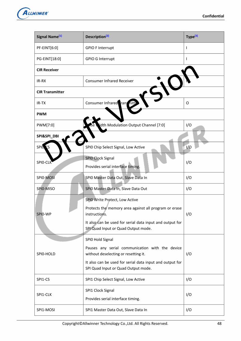
Confidential
Copyright© Allwinner Technology Co.,Ltd. All Rights Reserved. 48
Signal Name[1] Description[2] Type[3]
PF-EINT[6:0] GPIO F Interrupt I
PG-EINT[18:0] GPIO G Interrupt I
CIR Receiver
IR-RX Consumer Infrared Receiver I
CIR Transmitter
IR-TX Consumer Infrared Transmitter O
PWM
PWM[7:0] Pulse Width Modulation Output Channel [7:0] I/O
SPI&SPI_DBI
SPI0-CS SPI0 Chip Select Signal, Low Active I/O
SPI0-CLK SPI0 Clock Signal
Provides serial interface timing. I/O
SPI0-MOSI SPI0 Master Data Out, Slave Data In I/O
SPI0-MISO SPI0 Master Data In, Slave Data Out I/O
SPI0-WP
SPI0 Write Protect, Low Active
Protects the memory area against all program or erase
instructions.
It also can be used for serial data input and output for
SPI Quad Input or Quad Output mode.
I/O
SPI0-HOLD
SPI0 Hold Signal
Pauses any serial communication with the device
without deselecting or resetting it.
It also can be used for serial data input and output for
SPI Quad Input or Quad Output mode.
I/O
SPI1-CS SPI1 Chip Select Signal, Low Active I/O
SPI1-CLK SPI1 Clock Signal
Provides serial interface timing. I/O
SPI1-MOSI SPI1 Master Data Out, Slave Data In I/O
Draft Versio
n
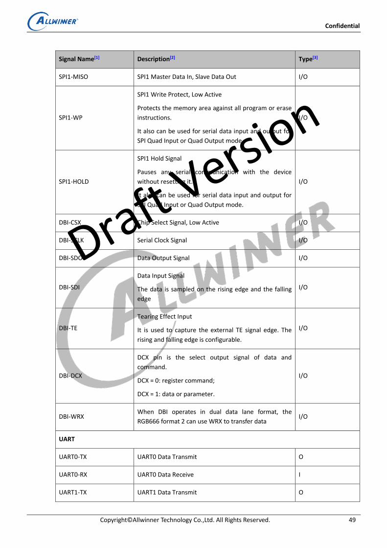
Confidential
Copyright© Allwinner Technology Co.,Ltd. All Rights Reserved. 49
Signal Name[1] Description[2] Type[3]
SPI1-MISO SPI1 Master Data In, Slave Data Out I/O
SPI1-WP
SPI1 Write Protect, Low Active
Protects the memory area against all program or erase
instructions.
It also can be used for serial data input and output for
SPI Quad Input or Quad Output mode.
I/O
SPI1-HOLD
SPI1 Hold Signal
Pauses any serial communication with the device
without resetting it.
It also can be used for serial data input and output for
SPI Quad Input or Quad Output mode.
I/O
DBI-CSX Chip Select Signal, Low Active I/O
DBI-SCLK Serial Clock Signal I/O
DBI-SDO Data Output Signal I/O
DBI-SDI
Data Input Signal
The data is sampled on the rising edge and the falling
edge
I/O
DBI-TE
Tearing Effect Input
It is used to capture the external TE signal edge. The
rising and falling edge is configurable.
I/O
DBI-DCX
DCX pin is the select output signal of data and
command.
DCX = 0: register command;
DCX = 1: data or parameter.
I/O
DBI-WRX When DBI operates in dual data lane format, the
RGB666 format 2 can use WRX to transfer data I/O
UART
UART0-TX UART0 Data Transmit O
UART0-RX UART0 Data Receive I
UART1-TX UART1 Data Transmit O
Draft Versio
n
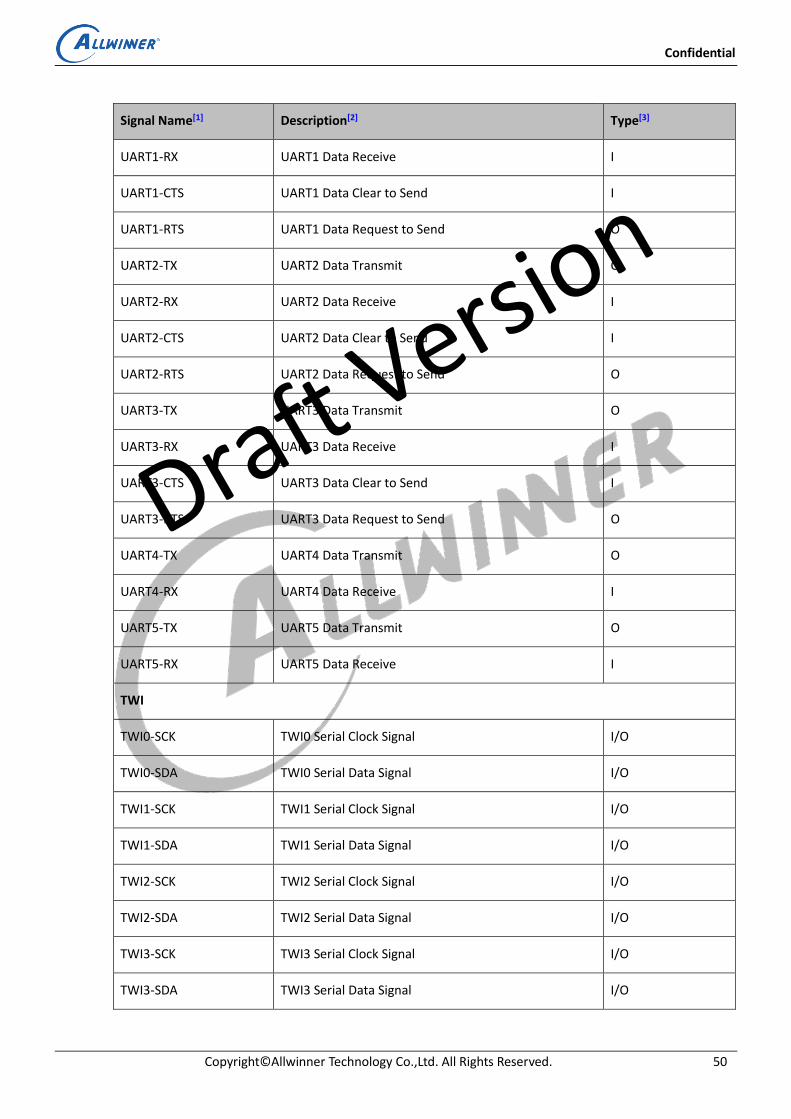
Confidential
Copyright© Allwinner Technology Co.,Ltd. All Rights Reserved. 50
Signal Name[1] Description[2] Type[3]
UART1-RX UART1 Data Receive I
UART1-CTS UART1 Data Clear to Send I
UART1-RTS UART1 Data Request to Send O
UART2-TX UART2 Data Transmit O
UART2-RX UART2 Data Receive I
UART2-CTS UART2 Data Clear to Send I
UART2-RTS UART2 Data Request to Send O
UART3-TX UART3 Data Transmit O
UART3-RX UART3 Data Receive I
UART3-CTS UART3 Data Clear to Send I
UART3-RTS UART3 Data Request to Send O
UART4-TX UART4 Data Transmit O
UART4-RX UART4 Data Receive I
UART5-TX UART5 Data Transmit O
UART5-RX UART5 Data Receive I
TWI
TWI0-SCK TWI0 Serial Clock Signal I/O
TWI0-SDA TWI0 Serial Data Signal I/O
TWI1-SCK TWI1 Serial Clock Signal I/O
TWI1-SDA TWI1 Serial Data Signal I/O
TWI2-SCK TWI2 Serial Clock Signal I/O
TWI2-SDA TWI2 Serial Data Signal I/O
TWI3-SCK TWI3 Serial Clock Signal I/O
TWI3-SDA TWI3 Serial Data Signal I/O
Draft Versio
n
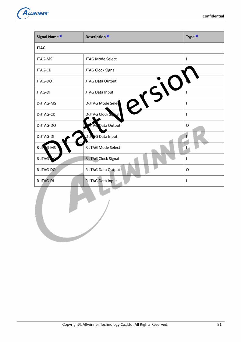
Confidential
Copyright© Allwinner Technology Co.,Ltd. All Rights Reserved. 51
Signal Name[1] Description[2] Type[3]
JTAG
JTAG-MS JTAG Mode Select I
JTAG-CK JTAG Clock Signal I
JTAG-DO JTAG Data Output O
JTAG-DI JTAG Data Input I
D-JTAG-MS D-JTAG Mode Select I
D-JTAG-CK D-JTAG Clock Signal I
D-JTAG-DO D-JTAG Data Output O
D-JTAG-DI D-JTAG Data Input I
R-JTAG-MS R-JTAG Mode Select I
R-JTAG-CK R-JTAG Clock Signal I
R-JTAG-DO R-JTAG Data Output O
R-JTAG-DI R-JTAG Data Input I
Draft Versio
n
Confidential
Copyright© Allwinner Technology Co.,Ltd. All Rights Reserved. 52
5 Electrical Characteristics
5.1 Parameter Conditions
5.1.1 Minimum and Maximum Values
Unless otherwise specified the minimum and maximum values are guaranteed in the worst conditions of
ambient temperature, supply voltage, and frequencies by tests in production on 100% of the devices with
ambient temperature at Ta = 25 °C and Ta = Ta max.
Data based on characterization results, design simulation, and/or technology characteristics are indicated in
the table footnotes and are not tested in production.
5.1.2 Typical Values
Unless otherwise specified, the typical data are based on Ta = 25 °C. They are given only as design guidelines.
5.1.3 Temperature Definitions
Ambient Temperature— the temperature of the surrounding environment.
Junction Temperature— the hottest temperature of the silicon chip inside the package.
Absolute Maximum Junction Temperature— the temperature beyond which damage occurs to the device.
The device may not function or meet expected performance at this temperature.
Recommended Operating Temperature— the junction temperature at which the device operates
continuously at the designated performance over the designed lifetime. The reliability of the device may
be degraded if the device operates above this temperature. Some devices will not function electrically
above this temperature.
5.2 Absolute Maximum Ratings
Absolute Maximum Ratings are those values beyond which damage to the device may occur. Table 5-1
specifies the absolute maximum ratings.
CAUTION
Stresses beyond those listed under Table 5-1 may affect reliability or cause permanent damage to the device.
These are stress ratings only. Functional operation of the device at these or any other conditions beyond
those indicated under Section 5.3, Recommended Operating Conditions, is not implied. Exposure to absolute
maximum rated conditions for extended periods may affect device reliability.
Draft Versio
n
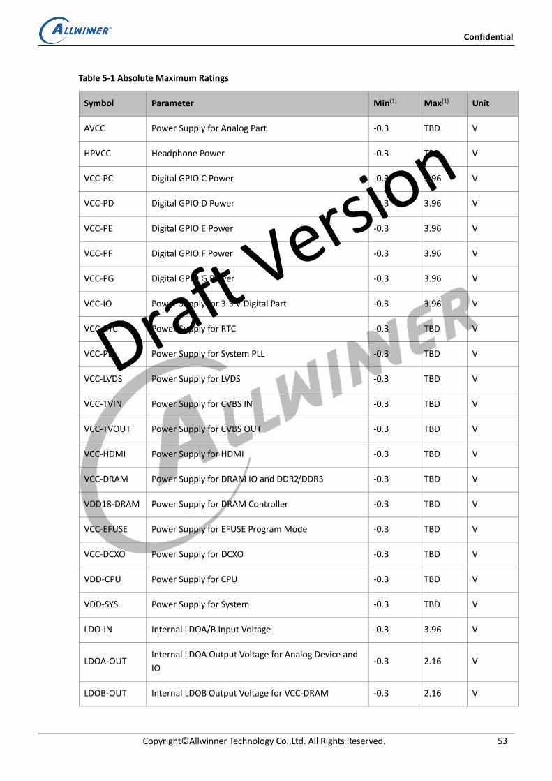
Confidential
Copyright© Allwinner Technology Co.,Ltd. All Rights Reserved. 53
Table 5-1 Absolute Maximum Ratings
Symbol Parameter Min(1) Max(1) Unit
AVCC Power Supply for Analog Part -0.3 TBD V
HPVCC Headphone Power -0.3 TBD V
VCC-PC Digital GPIO C Power -0.3 3.96 V
VCC-PD Digital GPIO D Power -0.3 3.96 V
VCC-PE Digital GPIO E Power -0.3 3.96 V
VCC-PF Digital GPIO F Power -0.3 3.96 V
VCC-PG Digital GPIO G Power -0.3 3.96 V
VCC-IO Power Supply for 3.3 V Digital Part -0.3 3.96 V
VCC-RTC Power Supply for RTC -0.3 TBD V
VCC-PLL Power Supply for System PLL -0.3 TBD V
VCC-LVDS Power Supply for LVDS -0.3 TBD V
VCC-TVIN Power Supply for CVBS IN -0.3 TBD V
VCC-TVOUT Power Supply for CVBS OUT -0.3 TBD V
VCC-HDMI Power Supply for HDMI -0.3 TBD V
VCC-DRAM Power Supply for DRAM IO and DDR2/DDR3 -0.3 TBD V
VDD18-DRAM Power Supply for DRAM Controller -0.3 TBD V
VCC-EFUSE Power Supply for EFUSE Program Mode -0.3 TBD V
VCC-DCXO Power Supply for DCXO -0.3 TBD V
VDD-CPU Power Supply for CPU -0.3 TBD V
VDD-SYS Power Supply for System -0.3 TBD V
LDO-IN Internal LDOA/B Input Voltage -0.3 3.96 V
LDOA-OUT Internal LDOA Output Voltage for Analog Device and
IO -0.3 2.16 V
LDOB-OUT Internal LDOB Output Voltage for VCC-DRAM -0.3 2.16 V
Draft Versio
n

Confidential
Copyright© Allwinner Technology Co.,Ltd. All Rights Reserved. 54
Symbol Parameter Min(1) Max(1) Unit
TSTG Storage Temperature -40 150 °C
Tj Working Junction Temperature -40 125 °C
VESD Electrostatic
Discharge(2)
Human Body Model(HBM)(3) TBD TBD V
Charged Device Model(CDM)(4) TBD TBD V
ILatch-up
Latch-up I-test performance current-pulse injection
on each IO pin(5) TBD
Latch-up over-voltage performance voltage injection
on each IO pin(6) TBD
(1) The min/max voltages of power rails are guaranteed by design, not tested in production.
(2) Electrostatic discharge (ESD) to measure device sensitivity/immunity to damage caused by electrostatic
discharges into the devices.
(3) Level listed above is the passing level per ESDA/JEDEC JS-001-2017.
(4) Level listed above is the passing level per ESDA/JEDEC JS-002-2018.
(5) Based on JESD78E; each device is tested with IO pin injection of ±200 mA at room temperature.
(6) Based on JESD78E; each device is tested with a stress voltage of 1.5 x Vddmax at room temperature.
5.3 Recommended Operating Conditions
Table 5-2 describes operating conditions of the D1.
NOTE
Logic functions and parameter values are not assured out of the range specified in the recommended
operating conditions.
Table 5-2 Recommended Operating Conditions
Symbol Parameter Min Typ Max Unit
Ta Ambient Operating Temperature -20 - 85 °C
Tj Working Junction Temperature Range -20 - TBD(1) °C
AVCC Power Supply for Analog Part 1.782 1.8 1.818 V
Draft Versio
n
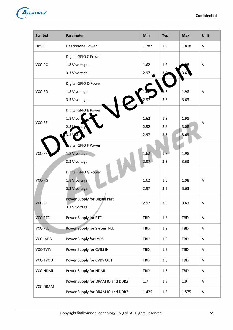
Confidential
Copyright© Allwinner Technology Co.,Ltd. All Rights Reserved. 55
Symbol Parameter Min Typ Max Unit
HPVCC Headphone Power 1.782 1.8 1.818 V
VCC-PC
Digital GPIO C Power
1.8 V voltage
3.3 V voltage
1.62
2.97
1.8
3.3
1.98
3.63
V
VCC-PD
Digital GPIO D Power
1.8 V voltage
3.3 V voltage
1.62
2.97
1.8
3.3
1.98
3.63
V
VCC-PE
Digital GPIO E Power
1.8 V voltage
2.8 V voltage
3.3 V voltage
1.62
2.52
2.97
1.8
2.8
3.3
1.98
3.08
3.63
V
VCC-PF
Digital GPIO F Power
1.8 V voltage
3.3 V voltage
1.62
2.97
1.8
3.3
1.98
3.63
VCC-PG
Digital GPIO G Power
1.8 V voltage
3.3 V voltage
1.62
2.97
1.8
3.3
1.98
3.63
V
VCC-IO Power Supply for Digital Part
3.3 V voltage 2.97 3.3 3.63 V
VCC-RTC Power Supply for RTC TBD 1.8 TBD V
VCC-PLL Power Supply for System PLL TBD 1.8 TBD V
VCC-LVDS Power Supply for LVDS TBD 1.8 TBD V
VCC-TVIN Power Supply for CVBS IN TBD 1.8 TBD V
VCC-TVOUT Power Supply for CVBS OUT TBD 3.3 TBD V
VCC-HDMI Power Supply for HDMI TBD 1.8 TBD V
VCC-DRAM
Power Supply for DRAM IO and DDR2 1.7 1.8 1.9 V
Power Supply for DRAM IO and DDR3 1.425 1.5 1.575 V
Draft Versio
n
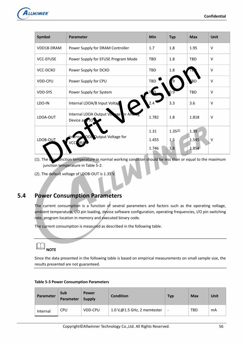
Confidential
Copyright© Allwinner Technology Co.,Ltd. All Rights Reserved. 56
Symbol Parameter Min Typ Max Unit
VDD18-DRAM Power Supply for DRAM Controller 1.7 1.8 1.95 V
VCC-EFUSE Power Supply for EFUSE Program Mode TBD 1.8 TBD V
VCC-DCXO Power Supply for DCXO TBD 1.8 TBD V
VDD-CPU Power Supply for CPU TBD 0.9 TBD V
VDD-SYS Power Supply for System TBD 0.9 TBD V
LDO-IN Internal LDOA/B Input Voltage 2.4 3.3 3.6 V
LDOA-OUT Internal LDOA Output Voltage for Analog
Device and IO 1.782 1.8 1.818 V
LDOB-OUT Internal LDOB Output Voltage for
VCC-DRAM
1.31
1.455
1.746
1.35(2)
1.5
1.8
1.39
1.545
1.854
V
(1). The chip junction temperature in normal working condition should be less than or equal to the maximum
junction temperature in Table 5-2.
(2). The default voltage of LDOB-OUT is 1.35 V.
5.4 Power Consumption Parameters
The current consumption is a function of several parameters and factors such as the operating voltage,
ambient temperature, I/O pin loading, device software configuration, operating frequencies, I/O pin switching
rate, program location in memory and executed binary code.
The current consumption is measured as described in the following table.
NOTE
Since the data presented in the following table is based on empirical measurements on small sample size, the
results presented are not guaranteed.
Table 5-3 Power Consumption Parameters
Parameter Sub
Parameter
Power
Supply Condition Typ Max Unit
Internal CPU VDD-CPU 1.0 V,@1.5 GHz, 2 memtester - TBD mA
Draft Versio
n
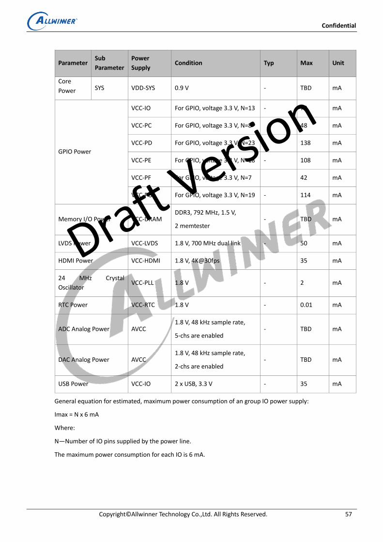
Confidential
Copyright© Allwinner Technology Co.,Ltd. All Rights Reserved. 57
Parameter Sub
Parameter
Power
Supply Condition Typ Max Unit
Core
Power SYS VDD-SYS 0.9 V - TBD mA
GPIO Power
VCC-IO For GPIO, voltage 3.3 V, N=13 - 78 mA
VCC-PC For GPIO, voltage 3.3 V, N=8 48 mA
VCC-PD For GPIO, voltage 3.3 V, N=23 - 138 mA
VCC-PE For GPIO, voltage 3.3 V, N=18 - 108 mA
VCC-PF For GPIO, voltage 3.3 V, N=7 42 mA
VCC-PG For GPIO, voltage 3.3 V, N=19 - 114 mA
Memory I/O Power VCC-DRAM DDR3, 792 MHz, 1.5 V,
2 memtester - TBD mA
LVDS Power VCC-LVDS 1.8 V, 700 MHz dual link - 50 mA
HDMI Power VCC-HDMI 1.8 V, 4K@30fps 35 mA
24 MHz Crystal
Oscillator VCC-PLL 1.8 V - 2 mA
RTC Power VCC-RTC 1.8 V - 0.01 mA
ADC Analog Power AVCC 1.8 V, 48 kHz sample rate,
5-chs are enabled - TBD mA
DAC Analog Power AVCC 1.8 V, 48 kHz sample rate,
2-chs are enabled - TBD mA
USB Power VCC-IO 2 x USB, 3.3 V - 35 mA
General equation for estimated, maximum power consumption of an group IO power supply:
Imax = N x 6 mA
Where:
N—Number of IO pins supplied by the power line.
The maximum power consumption for each IO is 6 mA.
Draft Versio
n
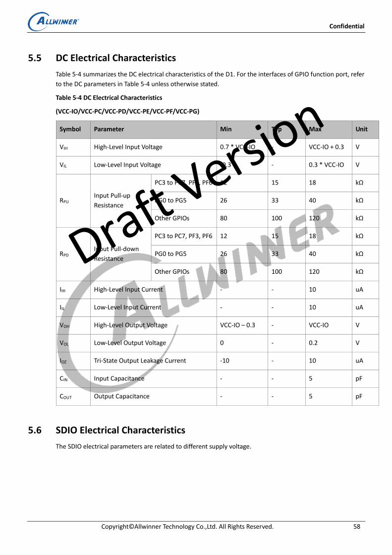
Confidential
Copyright© Allwinner Technology Co.,Ltd. All Rights Reserved. 58
5.5 DC Electrical Characteristics
Table 5-4 summarizes the DC electrical characteristics of the D1. For the interfaces of GPIO function port, refer
to the DC parameters in Table 5-4 unless otherwise stated.
Table 5-4 DC Electrical Characteristics
(VCC-IO/VCC-PC/VCC-PD/VCC-PE/VCC-PF/VCC-PG)
Symbol Parameter Min Typ Max Unit
VIH High-Level Input Voltage 0.7 * VCC-IO - VCC-IO + 0.3 V
VIL Low-Level Input Voltage -0.3 - 0.3 * VCC-IO V
RPU Input Pull-up
Resistance
PC3 to PC7, PF3, PF6 12 15 18 kΩ
PG0 to PG5 26 33 40 kΩ
Other GPIOs 80 100 120 kΩ
RPD Input Pull-down
Resistance
PC3 to PC7, PF3, PF6 12 15 18 kΩ
PG0 to PG5 26 33 40 kΩ
Other GPIOs 80 100 120 kΩ
IIH High-Level Input Current - - 10 uA
IIL Low-Level Input Current - - 10 uA
VOH High-Level Output Voltage VCC-IO – 0.3 - VCC-IO V
VOL Low-Level Output Voltage 0 - 0.2 V
IOZ Tri-State Output Leakage Current -10 - 10 uA
CIN Input Capacitance - - 5 pF
COUT Output Capacitance - - 5 pF
5.6 SDIO Electrical Characteristics
The SDIO electrical parameters are related to different supply voltage.
Draft Versio
n

Confidential
Copyright© Allwinner Technology Co.,Ltd. All Rights Reserved. 59
Figure 5-1 SDIO Voltage Waveform
Table 5-5 shows 3.3 V SDIO electrical parameters.
Table 5-5 3.3 V SDIO Electrical Parameters
Symbol Parameter Min Typ Max Unit
VDD Power voltage 2.7 - 3.6 V
VCCQ I/O voltage 2.7 3.6 V
VOH Output high-level voltage 0.75 * VCCQ - - V
VOL Output low-level voltage - - 0.125 * VCCQ V
VIH Input high-level voltage 0.625 * VCCQ - VCCQ + 0.3 V
VIL Input low-level voltage VSS – 0.3 - 0.25 * VCCQ V
Table 5-6 shows 1.8 V SDIO electrical parameters.
Table 5-6 1.8 V SDIO Electrical Parameters
Symbol Parameter Min Typ Max Unit
VDD Power voltage 2.7 - 3.6 V
VCCQ I/O voltage 1.7 1.95 V
VOH Output high-level voltage VCCQ – 0.45 - - V
VOL Output low-level voltage - - 0.45 V
VIH Input high-level voltage 0.625 * VCCQ (1) - VCCQ + 0.3 V
VIL Input low-level voltage VSS – 0.3 - 0.35 * VCCQ (2) V
Draft Versio
n
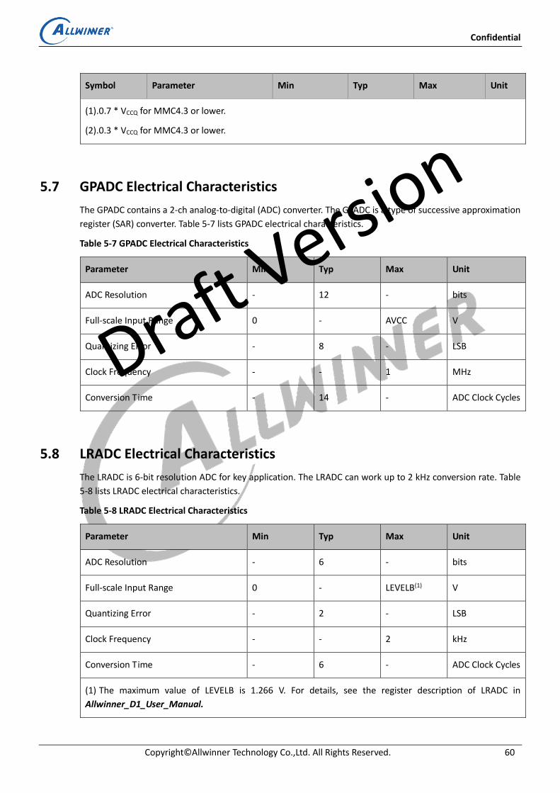
Confidential
Copyright© Allwinner Technology Co.,Ltd. All Rights Reserved. 60
Symbol Parameter Min Typ Max Unit
(1).0.7 * VCCQ for MMC4.3 or lower.
(2).0.3 * VCCQ for MMC4.3 or lower.
5.7 GPADC Electrical Characteristics
The GPADC contains a 2-ch analog-to-digital (ADC) converter. The GPADC is a type of successive approximation
register (SAR) converter. Table 5-7 lists GPADC electrical characteristics.
Table 5-7 GPADC Electrical Characteristics
Parameter Min Typ Max Unit
ADC Resolution - 12 - bits
Full-scale Input Range 0 - AVCC V
Quantizing Error - 8 - LSB
Clock Frequency - - 1 MHz
Conversion Time - 14 - ADC Clock Cycles
5.8 LRADC Electrical Characteristics
The LRADC is 6-bit resolution ADC for key application. The LRADC can work up to 2 kHz conversion rate. Table
5-8 lists LRADC electrical characteristics.
Table 5-8 LRADC Electrical Characteristics
Parameter Min Typ Max Unit
ADC Resolution - 6 - bits
Full-scale Input Range 0 - LEVELB(1) V
Quantizing Error - 2 - LSB
Clock Frequency - - 2 kHz
Conversion Time - 6 - ADC Clock Cycles
(1) The maximum value of LEVELB is 1.266 V. For details, see the register description of LRADC in
Allwinner_D1_User_Manual.
Draft Versio
n
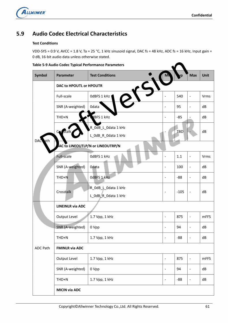
Confidential
Copyright© Allwinner Technology Co.,Ltd. All Rights Reserved. 61
5.9 Audio Codec Electrical Characteristics
Test Conditions
VDD-SYS = 0.9 V, AVCC = 1.8 V, Ta = 25 °C, 1 kHz sinusoid signal, DAC fs = 48 kHz, ADC fs = 16 kHz, Input gain =
0 dB, 16-bit audio data unless otherwise stated.
Table 5-9 Audio Codec Typical Performance Parameters
Symbol Parameter Test Conditions Min Typ Max Unit
DAC Path
DAC to HPOUTL or HPOUTR
Full-scale 0dBFS 1 kHz - 540 - Vrms
SNR (A-weighted) 0data - 95 - dB
THD+N 0dBFS 1 kHz - -85 - dB
Crosstalk R_0dB_L_0data 1 kHz
L_0dB_R_0data 1 kHz - TBD - dB
DAC to LINEOUTLP/N or LINEOUTRP/N
Full-scale 0dBFS 1 kHz - 1.1 - Vrms
SNR (A-weighted) 0data - 100 - dB
THD+N 0dBFS 1 kHz - -88 - dB
Crosstalk R_0dB_L_0data 1 kHz
L_0dB_R_0data 1 kHz - -105 - dB
ADC Path
LINEINLR via ADC
Output Level 1.7 Vpp, 1 kHz - 875 - mFFS
SNR (A-weighted) 0 Vpp - 94 - dB
THD+N 1.7 Vpp, 1 kHz - -88 - dB
FMINLR via ADC
Output Level 1.7 Vpp, 1 kHz - 875 - mFFS
SNR (A-weighted) 0 Vpp - 94 - dB
THD+N 1.7 Vpp, 1 kHz - -88 - dB
MICIN via ADC
Draft Versio
n

Confidential
Copyright© Allwinner Technology Co.,Ltd. All Rights Reserved. 62
Symbol Parameter Test Conditions Min Typ Max Unit
Output Level
MICP=3.3Vpp/2, MICN=3.3Vpp/2,
1 kHz, 0 dB Gain
- 880 - mFFS
SNR (A-weighted) - 98 - dB
THD+N - -90 - dB
Output Level
MICP=1.695Vpp/2, MICN=1.695Vpp/2,
1 kHz, 6 dB Gain
- 880 - mFFS
SNR (A-weighted) - 97 - dB
THD+N - -93 - dB
Output Level
MICP=0.788Vpp/2, MICN=0.788Vpp/2,
1 kHz,12 dB Gain
- 880 - mFFS
SNR (A-weighted) - 94 - dB
THD+N - -85 - dB
Output Level
MICP=0.392Vpp/2, MICN=0.392Vpp/2,
1 kHz, 18 dB Gain
- 880 - mFFS
SNR (A-weighted) - 92 - dB
THD+N - -83 - dB
Output Level
MICP=0.197Vpp/2, MICN=0.197Vpp/2,
1 kHz,24 dB Gain
- 880 - mFFS
SNR (A-weighted) - 87 - dB
THD+N - -80 - dB
Output Level
MICP=0.101Vpp/2, MICN=0.101Vpp/2,
1 kHz,30 dB Gain
- 880 - mFFS
SNR (A-weighted) - 82 - dB
THD+N - -73 - dB
Output Level
MICP=0.053Vpp/2, MICN=0.053Vpp/2,
1 kHz,36 dB Gain
- 880 - mFFS
SNR (A-weighted) - 76 - dB
THD+N - -65 - dB
MBIAS
Current - - 2.0 - mA
Voltage - 1.8 2.0 2.55 V
Noise 20 Hz—20 kHz - 3 - uV
Draft Versio
n
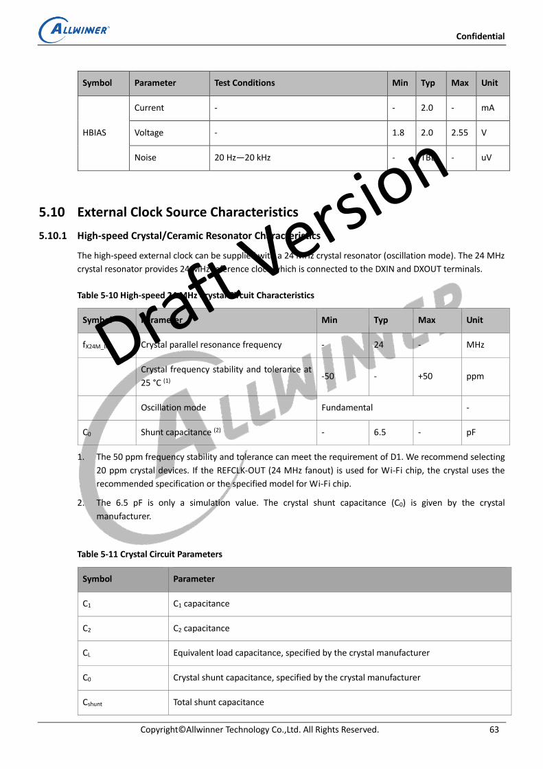
Confidential
Copyright© Allwinner Technology Co.,Ltd. All Rights Reserved. 63
Symbol Parameter Test Conditions Min Typ Max Unit
HBIAS
Current - - 2.0 - mA
Voltage - 1.8 2.0 2.55 V
Noise 20 Hz—20 kHz - TBD - uV
5.10 External Clock Source Characteristics
5.10.1 High-speed Crystal/Ceramic Resonator Characteristics
The high-speed external clock can be supplied with a 24 MHz crystal resonator (oscillation mode). The 24 MHz
crystal resonator provides 24 MHz reference clock which is connected to the DXIN and DXOUT terminals.
Table 5-10 High-speed 24 MHz Crystal Circuit Characteristics
Symbol Parameter Min Typ Max Unit
fX24M_IN Crystal parallel resonance frequency - 24 - MHz
Crystal frequency stability and tolerance at
25 °C (1) -50 - +50 ppm
Oscillation mode Fundamental -
C0 Shunt capacitance (2) - 6.5 - pF
1. The 50 ppm frequency stability and tolerance can meet the requirement of D1. We recommend selecting
20 ppm crystal devices. If the REFCLK-OUT (24 MHz fanout) is used for Wi-Fi chip, the crystal uses the
recommended specification or the specified model for Wi-Fi chip.
2. The 6.5 pF is only a simulation value. The crystal shunt capacitance (C0) is given by the crystal
manufacturer.
Table 5-11 Crystal Circuit Parameters
Symbol Parameter
C1 C1 capacitance
C2 C2 capacitance
CL Equivalent load capacitance, specified by the crystal manufacturer
C0 Crystal shunt capacitance, specified by the crystal manufacturer
Cshunt Total shunt capacitance
Draft Versio
n
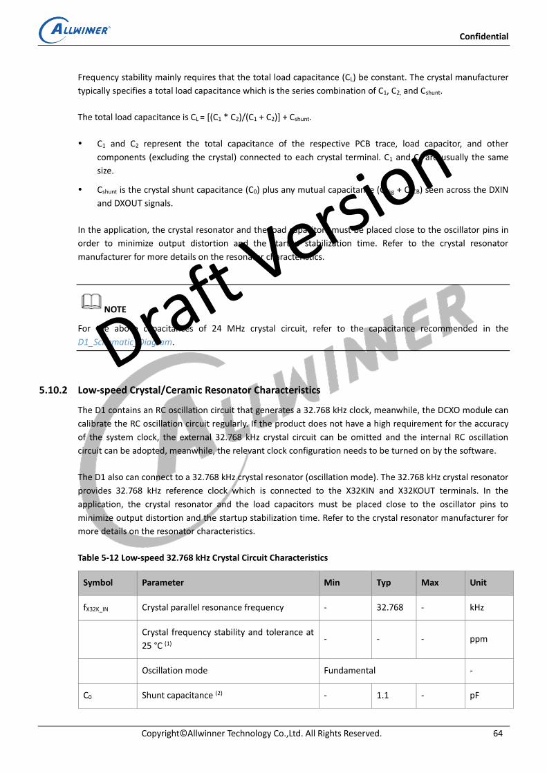
Confidential
Copyright© Allwinner Technology Co.,Ltd. All Rights Reserved. 64
Frequency stability mainly requires that the total load capacitance (CL) be constant. The crystal manufacturer
typically specifies a total load capacitance which is the series combination of C1, C2, and Cshunt.
The total load capacitance is CL = [(C1 * C2)/(C1 + C2)] + Cshunt.
C1 and C2 represent the total capacitance of the respective PCB trace, load capacitor, and other
components (excluding the crystal) connected to each crystal terminal. C1 and C2 are usually the same
size.
Cshunt is the crystal shunt capacitance (C0) plus any mutual capacitance (Cpkg + CPCB) seen across the DXIN
and DXOUT signals.
In the application, the crystal resonator and the load capacitors must be placed close to the oscillator pins in
order to minimize output distortion and the startup stabilization time. Refer to the crystal resonator
manufacturer for more details on the resonator characteristics.
NOTE
For the above capacitances of 24 MHz crystal circuit, refer to the capacitance recommended in the
D1_Schematic_Diagram.
5.10.2 Low-speed Crystal/Ceramic Resonator Characteristics
The D1 contains an RC oscillation circuit that generates a 32.768 kHz clock, meanwhile, the DCXO module can
calibrate the RC oscillation circuit regularly. If the product does not have a high requirement for the accuracy
of the system clock, the external 32.768 kHz crystal circuit can be omitted and the internal RC oscillation
circuit can be adopted, meanwhile, the relevant clock configuration needs to be turned on by the software.
The D1 also can connect to a 32.768 kHz crystal resonator (oscillation mode). The 32.768 kHz crystal resonator
provides 32.768 kHz reference clock which is connected to the X32KIN and X32KOUT terminals. In the
application, the crystal resonator and the load capacitors must be placed close to the oscillator pins to
minimize output distortion and the startup stabilization time. Refer to the crystal resonator manufacturer for
more details on the resonator characteristics.
Table 5-12 Low-speed 32.768 kHz Crystal Circuit Characteristics
Symbol Parameter Min Typ Max Unit
fX32K_IN Crystal parallel resonance frequency - 32.768 - kHz
Crystal frequency stability and tolerance at
25 °C (1) - - - ppm
Oscillation mode Fundamental -
C0 Shunt capacitance (2) - 1.1 - pF
Draft Versio
n

Confidential
Copyright© Allwinner Technology Co.,Ltd. All Rights Reserved. 65
1. The D1 has no requirement for the frequency stability and tolerance of 32.768 kHz crystal. If the actual
product has requirement for the accuracy of timing function, the 20 ppm stability and tolerance is
recommended.
2. The 1.1 pF is only a simulation value. The crystal shunt capacitance (C0) is given by the crystal
manufacturer.
NOTE
For capacitances of 32.768 kHz crystal circuit, refer to the capacitance recommended in the
D1_Schematic_Diagram.
5.11 Internal Reset Electrical Characteristics
Table 5-13 Internal Reset Electrical Characteristics
Parameter Test Condition Min Typ Max Unit
Power-on threshold voltage
of VDD-SYS on which the
reset signal is excited
Ta= -20°C to 85°C - TBD - V
Reset active timeout period Ta= -20°C to 85°C - TBD - ms
Reset open-drain output
voltage
Ta= -20°C to 85°C, pull up 3.3
V -0.3 - 0.3*VCC V
Power-off threshold voltage
of VCC-PL on which the reset
signal is excited
The voltage can be enabled by software, and it can be configured as 3.0 V,
2.9 V, 2.8 V, 2.7 V, 2.6 V, or 2.5 V.
5.12 External Memory Electrical Characteristics
5.12.1 SMHC AC Electrical Characteristics
(1) HS-SDR Mode
NOTE
IO voltage is 1.8 V or 3.3 V.
Draft Versio
n
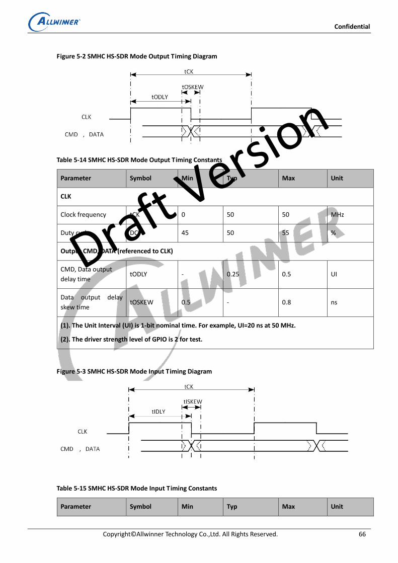
Confidential
Copyright© Allwinner Technology Co.,Ltd. All Rights Reserved. 66
Figure 5-2 SMHC HS-SDR Mode Output Timing Diagram
Table 5-14 SMHC HS-SDR Mode Output Timing Constants
Parameter Symbol Min Typ Max Unit
CLK
Clock frequency tCK 0 50 50 MHz
Duty cycle DC 45 50 55 %
Output CMD, DATA (referenced to CLK)
CMD, Data output
delay time tODLY - 0.25 0.5 UI
Data output delay
skew time tOSKEW 0.5 - 0.8 ns
(1). The Unit Interval (UI) is 1-bit nominal time. For example, UI=20 ns at 50 MHz.
(2). The driver strength level of GPIO is 2 for test.
Figure 5-3 SMHC HS-SDR Mode Input Timing Diagram
Table 5-15 SMHC HS-SDR Mode Input Timing Constants
Parameter Symbol Min Typ Max Unit
Draft Versio
n
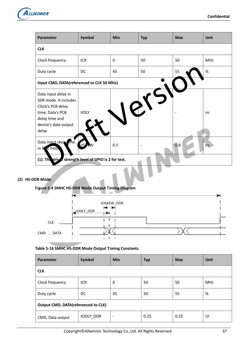
Confidential
Copyright© Allwinner Technology Co.,Ltd. All Rights Reserved. 67
Parameter Symbol Min Typ Max Unit
CLK
Clock frequency tCK 0 50 50 MHz
Duty cycle DC 45 50 55 %
Input CMD, DATA(referenced to CLK 50 MHz)
Data input delay in
SDR mode. It includes
Clock’s PCB delay
time, Data’s PCB
delay time and
device’s data output
delay
tIDLY - - - ns
Data input skew time
in SDR mode tISKEW 0.5 - 0.8 ns
(1). The driver strength level of GPIO is 2 for test.
(2) HS-DDR Mode
Figure 5-4 SMHC HS-DDR Mode Output Timing Diagram
Table 5-16 SMHC HS-DDR Mode Output Timing Constants
Parameter Symbol Min Typ Max Unit
CLK
Clock frequency tCK 0 50 50 MHz
Duty cycle DC 45 50 55 %
Output CMD, DATA(referenced to CLK)
CMD, Data output tODLY_DDR - 0.25 0.25 UI
Draft Versio
n

Confidential
Copyright© Allwinner Technology Co.,Ltd. All Rights Reserved. 68
Parameter Symbol Min Typ Max Unit
delay time in DDR
mode
Data output delay
skew time tOSKEW_DDR 0.5 - 0.8 ns
(1). The Unit Interval (UI) is 1-bit nominal time. For example, UI=20 ns at 50 MHz.
(2). The driver strength level of GPIO is 2 for test.
Figure 5-5 SMHC HS-DDR Mode Input Timing Diagram
Table 5-17 SMHC HS-DDR Mode Input Timing Constants
Parameter Symbol Min Typ Max Unit
CLK
Clock frequency tCK 0 50 50 MHz
Duty cycle DC 45 50 55 %
Input CMD, DATA (referenced to CLK 50 MHz)
Data input delay in
DDR mode. It
includes Clock’s PCB
delay time, Data’s
PCB delay time and
device’s data output
delay
tIDLY_DDR - - - ns
Data input skew time
in DDR mode tISKEW_DDR 0.5 - 0.8 ns
(1). The driver strength level of GPIO is 2 for test.
Draft Versio
n
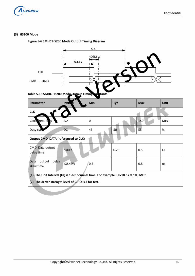
Confidential
Copyright© Allwinner Technology Co.,Ltd. All Rights Reserved. 69
(3) HS200 Mode
Figure 5-6 SMHC HS200 Mode Output Timing Diagram
Table 5-18 SMHC HS200 Mode Output Timing Constants
Parameter Symbol Min Typ Max Unit
CLK
Clock frequency tCK 0 - 150 MHz
Duty cycle DC 45 50 55 %
Output CMD, DATA (referenced to CLK)
CMD, Data output
delay time tODLY - 0.25 0.5 UI
Data output delay
skew time tOSKEW 0.5 - 0.8 ns
(1). The Unit Interval (UI) is 1-bit nominal time. For example, UI=10 ns at 100 MHz.
(2). The driver strength level of GPIO is 3 for test.
Draft Versio
n
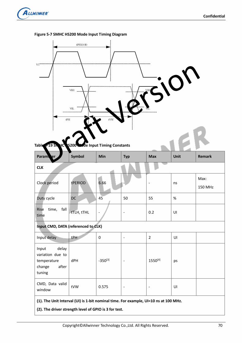
Confidential
Copyright© Allwinner Technology Co.,Ltd. All Rights Reserved. 70
Figure 5-7 SMHC HS200 Mode Input Timing Diagram
Table 5-19 SMHC HS200 Mode Input Timing Constants
Parameter Symbol Min Typ Max Unit Remark
CLK
Clock period tPERIOD 6.66 - - ns Max:
150 MHz
Duty cycle DC 45 50 55 %
Rise time, fall
time tTLH, tTHL - - 0.2 UI
Input CMD, DATA (referenced to CLK)
Input delay tPH 0 - 2 UI
Input delay
variation due to
temperature
change after
tuning
dPH -350[3] - 1550[4] ps
CMD, Data valid
window tVW 0.575 - - UI
(1). The Unit Interval (UI) is 1-bit nominal time. For example, UI=10 ns at 100 MHz.
(2). The driver strength level of GPIO is 3 for test.
Draft Versio
n
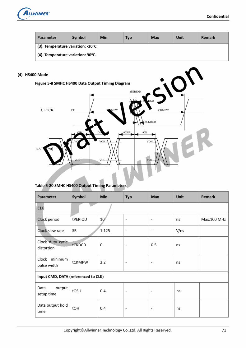
Confidential
Copyright© Allwinner Technology Co.,Ltd. All Rights Reserved. 71
Parameter Symbol Min Typ Max Unit Remark
(3). Temperature variation: -20oC.
(4). Temperature variation: 90oC.
(4) HS400 Mode
Figure 5-8 SMHC HS400 Data Output Timing Diagram
tPERIOD
VT tCKMPW tCKMPW
tCKDCD
tCKDCD
tOSU tOH tOSU tOH
VOH
VOL
VOH
VOL
VOH
VOL
CLOCK
DATA[7:0]
Table 5-20 SMHC HS400 Output Timing Parameters
Parameter Symbol Min Typ Max Unit Remark
CLK
Clock period tPERIOD 10 - - ns Max:100 MHz
Clock slew rate SR 1.125 - - V/ns
Clock duty cycle
distortion tCKDCD 0 - 0.5 ns
Clock minimum
pulse width tCKMPW 2.2 - - ns
Input CMD, DATA (referenced to CLK)
Data output
setup time tOSU 0.4 - - ns
Data output hold
time tOH 0.4 - - ns
Draft Versio
n
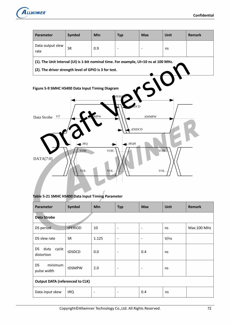
Confidential
Copyright© Allwinner Technology Co.,Ltd. All Rights Reserved. 72
Parameter Symbol Min Typ Max Unit Remark
Data output slew
rate SR 0.9 - - ns
(1). The Unit Interval (UI) is 1-bit nominal time. For example, UI=10 ns at 100 MHz.
(2). The driver strength level of GPIO is 3 for test.
Figure 5-9 SMHC HS400 Data Input Timing Diagram
tPERIOD
VT tDSMPW tDSMPW
tDSDCD
tDSDCD
tRQHtRQ
VOH
VOL
VOH
VOL
VOH
VOL
Data Strobe
DATA[7:0]
Table 5-21 SMHC HS400 Data Input Timing Parameter
Parameter Symbol Min Typ Max Unit Remark
Data Strobe
DS period tPERIOD 10 - - ns Max:100 MHz
DS slew rate SR 1.125 - - V/ns
DS duty cycle
distortion tDSDCD 0.0 - 0.4 ns
DS minimum
pulse width tDSMPW 2.0 - - ns
Output DATA (referenced to CLK)
Data input skew tRQ - - 0.4 ns
Draft Versio
n

Confidential
Copyright© Allwinner Technology Co.,Ltd. All Rights Reserved. 73
Parameter Symbol Min Typ Max Unit Remark
Data input hold
skew tRQH - - 0.4 ns
Data input slew
rate SR 0.85 - - V/ns
(1). The Unit Interval (UI) is 1-bit nominal time. For example, UI=10 ns at 100 MHz.
(2). The driver strength level of GPIO is 3 for test.
5.13 External Peripheral Electrical Characteristics
5.13.1 EMAC AC Electrical Characteristics
5.13.1.1 RGMII
Figure 5-10 RGMII Interface Transmit Timing
Tclk
RGMII_TX_CLK
RGMII/TBI Input
Tisu Tiph
Topv
Toph
RGMII Output
Table 5-22 RGMII Transmit Timing Constants
Parameter Symbol Min Typ Max Unit
RGMII_TX_CLK clock period Tclk 8 - DC ns
RGMII/TBI input setup prior to
RGMII_TX_CLK Tisu 2.8 - - ns
RGMII/TBI input data hold after
RGMII_TX_CLK Tiph 0.1 - - ns
RGMII output data valid after
RGMII_TX_CLK Topv - - 0.85 ns
RGMII output data hold after Toph 0 - - ns
Draft Versio
n
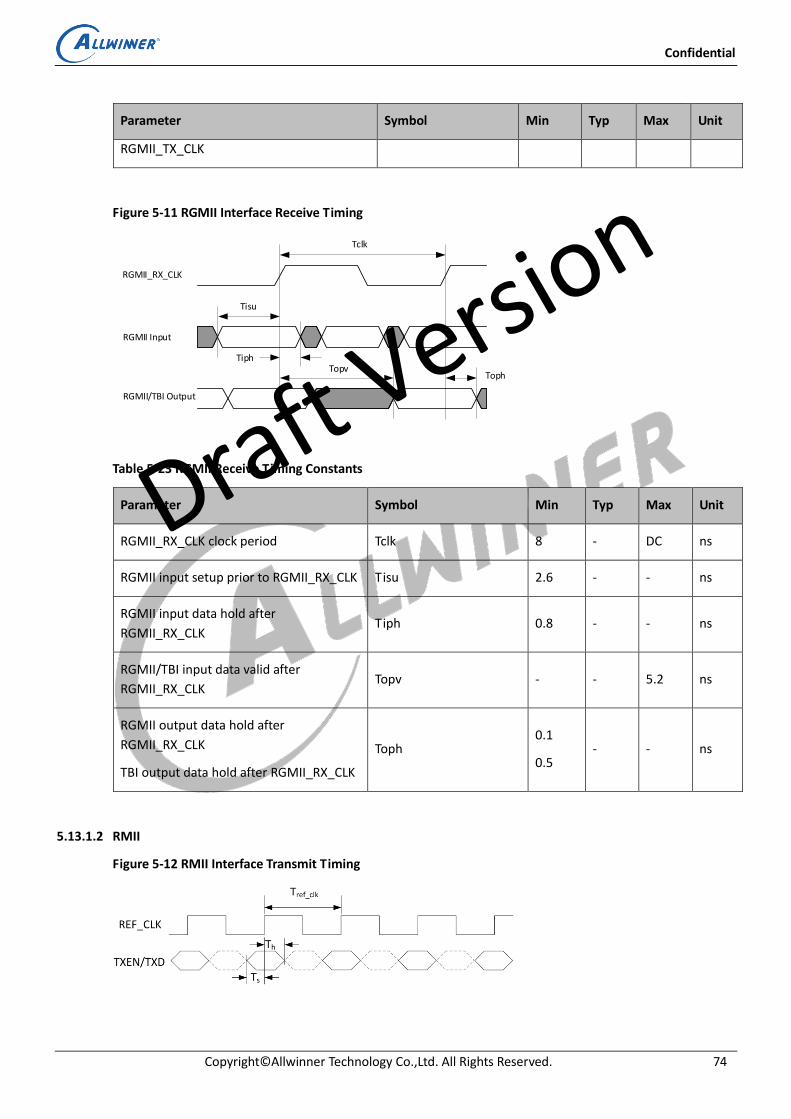
Confidential
Copyright© Allwinner Technology Co.,Ltd. All Rights Reserved. 74
Parameter Symbol Min Typ Max Unit
RGMII_TX_CLK
Figure 5-11 RGMII Interface Receive Timing
Tclk
RGMII_RX_CLK
Tisu
RGMII Input
TiphTopv
Toph
RGMII/TBI Output
Table 5-23 RGMII Receive Timing Constants
Parameter Symbol Min Typ Max Unit
RGMII_RX_CLK clock period Tclk 8 - DC ns
RGMII input setup prior to RGMII_RX_CLK Tisu 2.6 - - ns
RGMII input data hold after
RGMII_RX_CLK Tiph 0.8 - - ns
RGMII/TBI input data valid after
RGMII_RX_CLK Topv - - 5.2 ns
RGMII output data hold after
RGMII_RX_CLK
TBI output data hold after RGMII_RX_CLK
Toph 0.1
0.5 - - ns
5.13.1.2 RMII
Figure 5-12 RMII Interface Transmit Timing
Draft Versio
n

Confidential
Copyright© Allwinner Technology Co.,Ltd. All Rights Reserved. 75
Table 5-24 RMII Transmit Timing Constants
Parameter Symbol Min Typ Max Unit
Reference clock period Tref_clk - 20 - ns
TXD/TXEN to REF_CLK setup time Ts 4 - - ns
TXD/TXEN to REF_CLK hold time Th 2 - - ns
Figure 5-13 RMII Interface Receive Timing
Table 5-25 RMII Receive Timing Constants
Parameter Symbol Min Typ Max Unit
Reference clock period Tref_clk - 20 - ns
REF_CLK rising edge to RX_DV/RXD Td - 10 12 ns
5.13.2 SPI AC Electrical Characteristics
Figure 5-14 SPI Writing Timing
CS#
SCLK
MOSI
MISO
ts(cs)
th(cs)
MSB LSB
th(mo) tv(mo)
Draft Versio
n
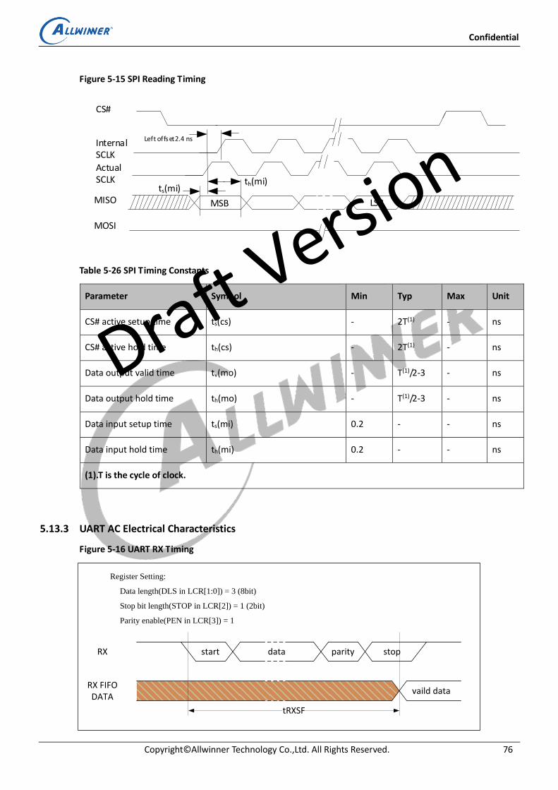
Confidential
Copyright© Allwinner Technology Co.,Ltd. All Rights Reserved. 76
Figure 5-15 SPI Reading Timing
CS#
MISO
MOSI
MSB LSB
Internal SCLK
ActualSCLK
Left offset2.4 ns
ts(mi)th(mi)
Table 5-26 SPI Timing Constants
Parameter Symbol Min Typ Max Unit
CS# active setup time ts(cs) - 2T(1) - ns
CS# active hold time th(cs) - 2T(1) - ns
Data output valid time tv(mo) - T(1)/2-3 - ns
Data output hold time th(mo) - T(1)/2-3 - ns
Data input setup time ts(mi) 0.2 - - ns
Data input hold time th(mi) 0.2 - - ns
(1).T is the cycle of clock.
5.13.3 UART AC Electrical Characteristics
Figure 5-16 UART RX Timing
start data parity stop
vaild data
tRXSF
RX
RX FIFO DATA
Register Setting:
Data length(DLS in LCR[1:0]) = 3 (8bit)
Stop bit length(STOP in LCR[2]) = 1 (2bit)
Parity enable(PEN in LCR[3]) = 1
Draft Versio
n
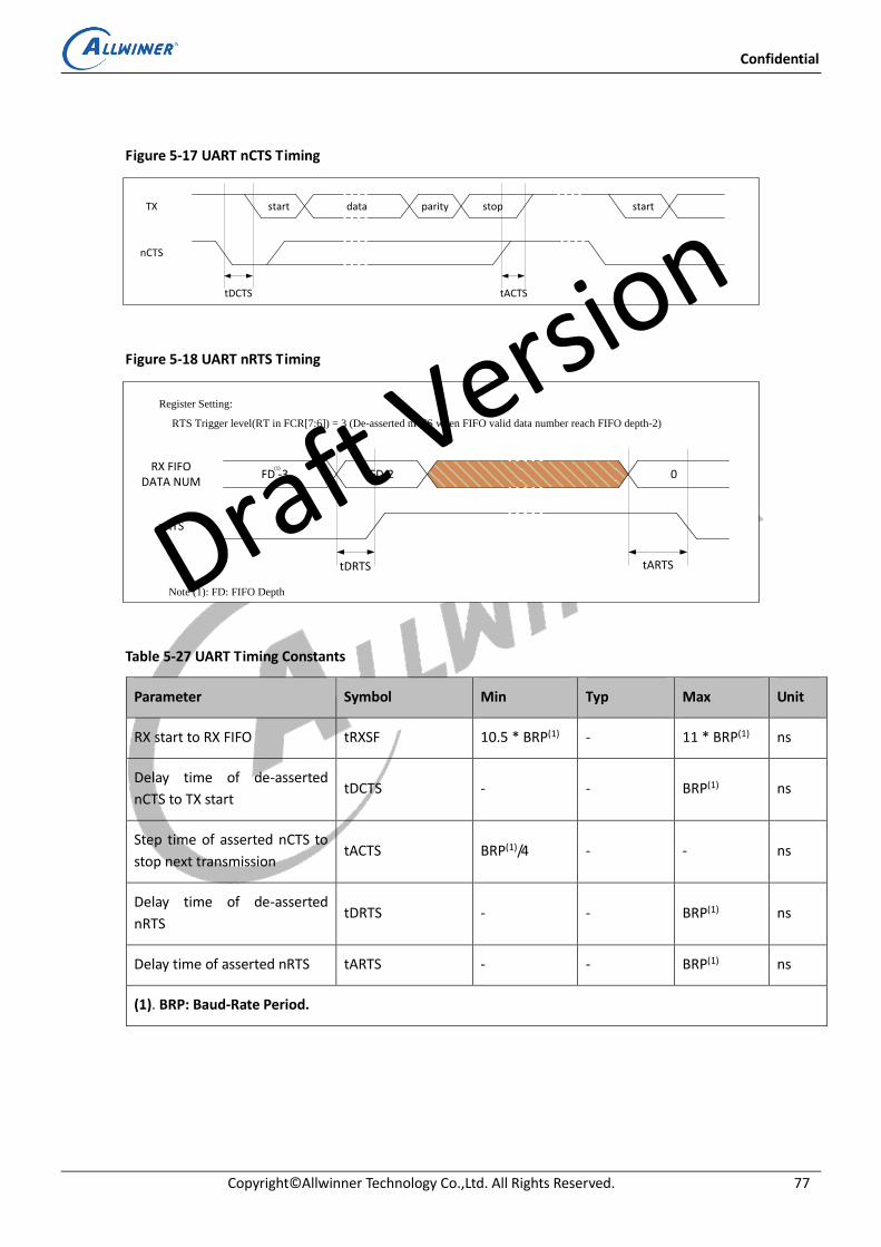
Confidential
Copyright© Allwinner Technology Co.,Ltd. All Rights Reserved. 77
Figure 5-17 UART nCTS Timing
data parity stop TX
nCTS
start
tDCTS tACTS
start
Figure 5-18 UART nRTS Timing
FD -3
tDRTS tARTS
RX FIFO DATA NUM
nRTS
FD-2 0
Register Setting:
RTS Trigger level(RT in FCR[7:6]) = 3 (De-asserted nRTS when FIFO valid data number reach FIFO depth-2)
(1)
Note (1): FD: FIFO Depth
Table 5-27 UART Timing Constants
Parameter Symbol Min Typ Max Unit
RX start to RX FIFO tRXSF 10.5 * BRP(1) - 11 * BRP(1) ns
Delay time of de-asserted
nCTS to TX start tDCTS - - BRP(1) ns
Step time of asserted nCTS to
stop next transmission tACTS BRP(1)/4 - - ns
Delay time of de-asserted
nRTS tDRTS - - BRP(1) ns
Delay time of asserted nRTS tARTS - - BRP(1) ns
(1). BRP: Baud-Rate Period.
Draft Versio
n
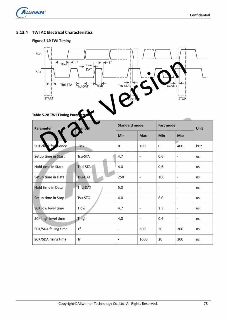
Confidential
Copyright© Allwinner Technology Co.,Ltd. All Rights Reserved. 78
5.13.4 TWI AC Electrical Characteristics
Figure 5-19 TWI Timing
Table 5-28 TWI Timing Parameters
Parameter Symbol Standard mode Fast mode
Unit
Min Max Min Max
SCK clock frequency Fsck 0 100 0 400 kHz
Setup time in Start Tsu-STA 4.7 - 0.6 - us
Hold time in Start Thd-STA 4.0 - 0.6 - us
Setup time in Data Tsu-DAT 250 - 100 - ns
Hold time in Data Thd-DAT 5.0 - - - ns
Setup time in Stop Tsu-STO 4.0 - 6.0 - us
SCK low level time Tlow 4.7 - 1.3 - us
SCK high level time Thigh 4.0 - 0.6 - ns
SCK/SDA falling time Tf - 300 20 300 ns
SCK/SDA rising time Tr - 1000 20 300 ns
Draft Versio
n
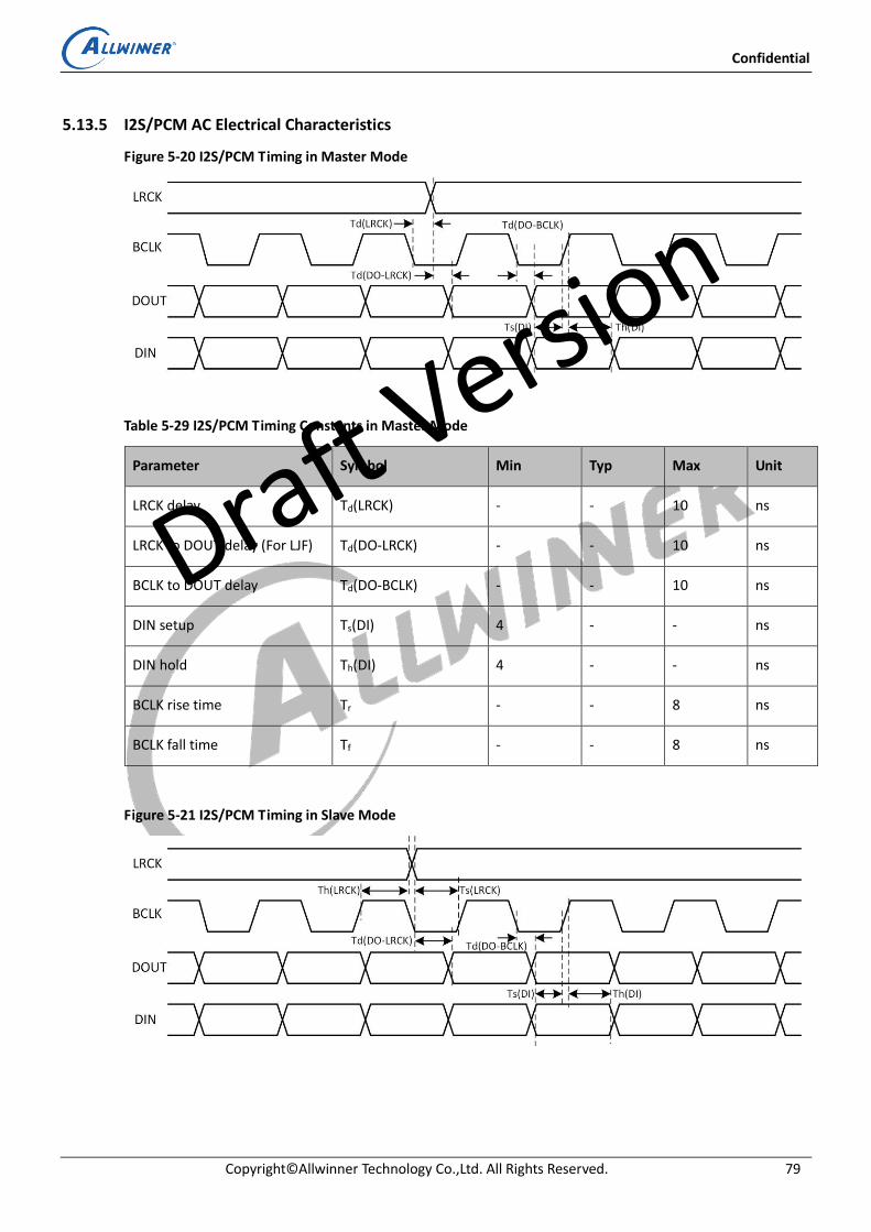
Confidential
Copyright© Allwinner Technology Co.,Ltd. All Rights Reserved. 79
5.13.5 I2S/PCM AC Electrical Characteristics
Figure 5-20 I2S/PCM Timing in Master Mode
Table 5-29 I2S/PCM Timing Constants in Master Mode
Parameter Symbol Min Typ Max Unit
LRCK delay Td(LRCK) - - 10 ns
LRCK to DOUT delay (For LJF) Td(DO-LRCK) - - 10 ns
BCLK to DOUT delay Td(DO-BCLK) - - 10 ns
DIN setup Ts(DI) 4 - - ns
DIN hold Th(DI) 4 - - ns
BCLK rise time Tr - - 8 ns
BCLK fall time Tf - - 8 ns
Figure 5-21 I2S/PCM Timing in Slave Mode
Draft Versio
n
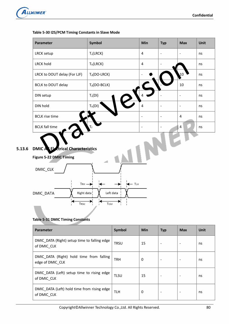
Confidential
Copyright© Allwinner Technology Co.,Ltd. All Rights Reserved. 80
Table 5-30 I2S/PCM Timing Constants in Slave Mode
Parameter Symbol Min Typ Max Unit
LRCK setup Ts(LRCK) 4 - - ns
LRCK hold Th(LRCK) 4 - - ns
LRCK to DOUT delay (For LJF) Td(DO-LRCK) - - 10 ns
BCLK to DOUT delay Td(DO-BCLK) - - 10 ns
DIN setup Ts(DI) 4 - - ns
DIN hold Th(DI) 4 - - ns
BCLK rise time Tr - - 4 ns
BCLK fall time Tf - - 4 ns
5.13.6 DMIC AC Electrical Characteristics
Figure 5-22 DMIC Timing
Table 5-31 DMIC Timing Constants
Parameter Symbol Min Typ Max Unit
DMIC_DATA (Right) setup time to falling edge
of DMIC_CLK TRSU 15 - - ns
DMIC_DATA (Right) hold time from falling
edge of DMIC_CLK TRH 0 - - ns
DMIC_DATA (Left) setup time to rising edge
of DMIC_CLK TLSU 15 - - ns
DMIC_DATA (Left) hold time from rising edge
of DMIC_CLK TLH 0 - - ns
Draft Versio
n
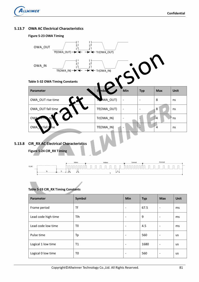
Confidential
Copyright© Allwinner Technology Co.,Ltd. All Rights Reserved. 81
5.13.7 OWA AC Electrical Characteristics
Figure 5-23 OWA Timing
Tr(OWA_OUT)Tf(OWA_OUT)
Tr(OWA_IN)Tf(OWA_IN)
OWA_OUT
OWA_IN
Table 5-32 OWA Timing Constants
Parameter Symbol Min Typ Max Unit
OWA_OUT rise time Tr(OWA_OUT) - - 8 ns
OWA_OUT fall time Tf(OWA_OUT) - - 8 ns
OWA_IN rise time Tr(OWA_IN) - - 4 ns
OWA_IN fall time Tf(OWA_IN) - - 4 ns
5.13.8 CIR_RX AC Electrical Characteristics
Figure 5-24 CIR_RX Timing
Tlh Tll Tp T0T1
Address #Address Command #Command
Tf
IR_NEC
Table 5-33 CIR_RX Timing Constants
Parameter Symbol Min Typ Max Unit
Frame period Tf - 67.5 - ms
Lead code high time Tlh - 9 - ms
Lead code low time Tll - 4.5 - ms
Pulse time Tp - 560 - us
Logical 1 low time T1 - 1680 - us
Logical 0 low time T0 - 560 - us
Draft Versio
n

Confidential
Copyright© Allwinner Technology Co.,Ltd. All Rights Reserved. 82
5.14 Power-On and Power-Off Sequence
5.14.1 Power-On Sequence
Figure 5-25 shows an example of the power-on sequence for the D1 device. The description of the power-on
sequence is as follows.
• The consequent steps in power-on sequence should not start before the previous step supplies have
been stabilized within 90~110% of their nominal voltage, unless stated otherwise.
• VCC-RTC must be ramped no later than other power rails.
• VCC-IO must be ramped before VDD-SYS and VDD-CPU with a minimum delay of 2 ms.
• VCC-DRAM needs be stable before SDRAM driver initialization.
• During the entire power on sequence, the RESET signal must be held on low until all other power rails
(except 24 MHz CLK) are stable for more than 64 ms.
• 24 MHz clock starts oscillating after the RESET signal is released.
Figure 5-25 Power-On Timing
VDD-CPU
VCC-PLLVCC-TVINVCC-HDMIVCC-LVDSVDD18-DRAM
24M CLK
RESET
1.8 V
0.9 V
10%
VCC-PCVCC-PEVCC-PFVCC-PG
VCC-IOVCC-PDVCC-TVOUTLDOINHPLDOIN
1.8 V/3.3 V
3.3 V
VDD-SYS
0.9 VT1>2 ms
90%
90%
VCC-DRAM
1.8 V/1.5 V
VCC-RTC 90%
90%
90%
90%
90%
5.14.2 Power-Off Sequence
The power-off requirements are as follows.
Draft Versio
n
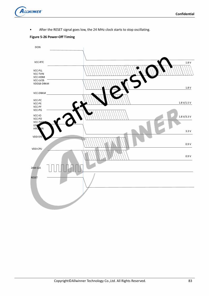
Confidential
Copyright© Allwinner Technology Co.,Ltd. All Rights Reserved. 83
• After the RESET signal goes low, the 24 MHz clock starts to stop oscillating.
Figure 5-26 Power-Off Timing
VDD-SYS
VCC-PLLVCC-TVINVCC-HDMIVCC-LVDSVDD18-DRAM
24M CLK
1.8 V/1.5 V
0.9 V
VCC-PCVCC-PEVCC-PFVCC-PG
VCC-IOVCC-PDVCC-TVOUTLDOINHPLDOIN
1.8 V/3.3 V
3.3 V
VDD-CPU
0.9 V
DCIN
VCC-DRAM
1.8 V
VCC-RTC 1.8 V
RESET
Draft Versio
n
Confidential
Copyright© Allwinner Technology Co.,Ltd. All Rights Reserved. 84
6 Package Thermal Characteristics The maximum chip junction temperature (TJ max) must never exceed the values given in Table 5-2
Recommended Operating Conditions.
The maximum chip-junction temperature TJ max, in degrees Celsius, may be calculated using the following
equation:
TJ max = Ta max + (PD max x θJA)
Where:
Ta max is the maximum ambient temperature in °C.
PD max is the maximum power dissipation.
θJA is the package junction-to-ambient thermal resistance, in °C/W.
°C/W = degrees Celsius per watt.
Failure to maintain a junction temperature within the range specified reduces operating lifetime, reliability,
and performance, and may cause irreversible damage to the system. It is useful to calculate the exact power
consumption and junction temperature to determine which the temperature will be best suited to the
application. Therefore, the product should include thermal analysis and thermal design to ensure the
operating junction temperature of the device is within functional limits.
The following table shows the thermal resistance characteristics of the D1. These data are based on JEDEC
JESD51 standard, because the actual system design and temperature could be different from JEDEC JESD51,
these simulating data are a reference only and may not represent actual use-case values, please prevail in the
actual application condition test.
Table 6-1 D1 Package Thermal Characteristics
Symbol Parameter Min Typ(1) Max Unit
θJA Junction-to-Ambient Thermal Resistance - TBD - °C/W
θJB Junction-to-Board Thermal Resistance - TBD - °C/W
θJC Junction-to-Case Thermal Resistance - TBD - °C/W
1. Reference document: JESD51-2 Integrated Circuits Thermal Test Method Environment Conditions – Natural
Convection (Still Air). Available from www.jedec.org.
Draft Versio
n

Confidential
Copyright© Allwinner Technology Co.,Ltd. All Rights Reserved. 85
7 Pin Assignment
7.1 Pin Map
For D1, LFBAG 337 balls, 13 mm x 13 mm package is offered. The following figure shows the pin map of the
D1.
Figure 7-1 D1 Pin Map
Draft Versio
n

Confidential
Copyright© Allwinner Technology Co.,Ltd. All Rights Reserved. 86
7.2 Package Dimension
Figure 7-2 shows the top, bottom, and side views of D1 package dimension.
Figure 7-2 D1 Package Dimension
Draft Versio
n
Confidential
Copyright© Allwinner Technology Co.,Ltd. All Rights Reserved. 87
8 Carrier, Storage and Baking Information
8.1 Carrier
8.1.1 Matrix Tray Information
Table 8-1 shows the D1 matrix tray carrier information.
Table 8-1 Matrix Tray Carrier Information
Item Color Size Note
Tray Black 315 mm x 136 mm x 7.62 mm 119 Qty/Tray
Aluminum foil bags Silvery
white 540 mm x 300 mm x 0.14 mm
Vacuum packing
Including HIC and desiccant
Printing: RoHS symbol
Pearl cotton cushion
(Vacuum bag) White 12 mm x 680 mm x 185 mm
Pearl cotton cushion
(The Gap between
vacuum bag and inner
box)
White
Left-Right:
12 mm x 180 mm x 85 mm
Front-Back:
12 mm x 350 mm x 70 mm
Inner Box White 396 mm x 196 mm x 96 mm Printing: RoHS symbol
10 Tray/Inner box
Carton White 420 mm x 410 mm x 320 mm 6 Inner box/Carton
Table 8-2 shows the D1 packing quantity.
Table 8-2 D1 Packing Quantity Information
Sample Size (mm) Qty/Tray Tray/Inner Box Full Inner Box
Qty
Inner
Box/Carton
Full Carton
Qty
D1 13 x 13 119 10 1190 6 7140
Figure 8-1 shows tray dimension drawing of the D1.
Draft Versio
n

Confidential
Copyright© Allwinner Technology Co.,Ltd. All Rights Reserved. 88
Figure 8-1 D1 Tray Dimension Drawing
8.2 Storage
Reliability is affected if any condition specified in Section 8.2.2 and Section 8.2.3 has been exceeded.
8.2.1 Moisture Sensitivity Level (MSL)
A package’s MSL indicates its ability to withstand exposure after it is removed from its shipment bag, a low
MSL device sample can be exposed on the factory floor longer than a high MSL device sample. Table 8-3
defines all MSL.
The D1 device samples are classified as MSL3.
Table 8-3 MSL Summary
MSL Out-of-bag floor life Comments
1 Unlimited ≤30°C / 85%RH
2 1 year ≤30°C / 60%RH
2a 4 weeks ≤30°C / 60%RH
3 168 hours ≤30°C / 60%RH
4 72 hours ≤30°C / 60%RH
NOTE
Draft Versio
n

Confidential
Copyright© Allwinner Technology Co.,Ltd. All Rights Reserved. 89
MSL Out-of-bag floor life Comments
5 48 hours ≤30°C / 60%RH
5a 24 hours ≤30°C / 60%RH
6 Time on Label (TOL) ≤30°C / 60%RH
8.2.2 Bagged Storage Conditions
Table 8-4 defines the shelf life of the D1 device samples.
Table 8-4 Bagged Storage Conditions
Packing mode Vacuum packing
Storage temperature 20–26°C
Storage humidity 40%–60%RH
Shelf life 12 months
8.2.3 Out-of-bag Duration
It is defined by the device MSL rating. The out-of-bag duration of the D1 is as follows.
Table 8-5 Out-of-bag Duration
Storage temperature 20–26°C
Storage humidity 40%–60%RH
Moisture sensitive level (MSL) 3
Floor life 168 hours
For no mention of storage rules in this document, refer to the latest IPC/JEDEC J-STD-020C.
8.3 Baking
It is not necessary to bake the D1 if the conditions specified in Section 8.2.2 and Section 8.2.3 have not been
exceeded. It is necessary to bake the D1 if any condition specified in Section 8.2.2 and Section 8.2.3 has been
exceeded.
Draft Versio
n

Confidential
Copyright© Allwinner Technology Co.,Ltd. All Rights Reserved. 90
It is necessary to bake the D1 if the storage humidity condition has been exceeded, we recommend that the
device sample removed from its shipment bag for more than 2 days shall be baked to guarantee production.
Baking conditions: 125°C, 8 hours, nitrogen protection. Note that the baking should not exceed 1 times due to
a risk of deformation.
Draft Versio
n
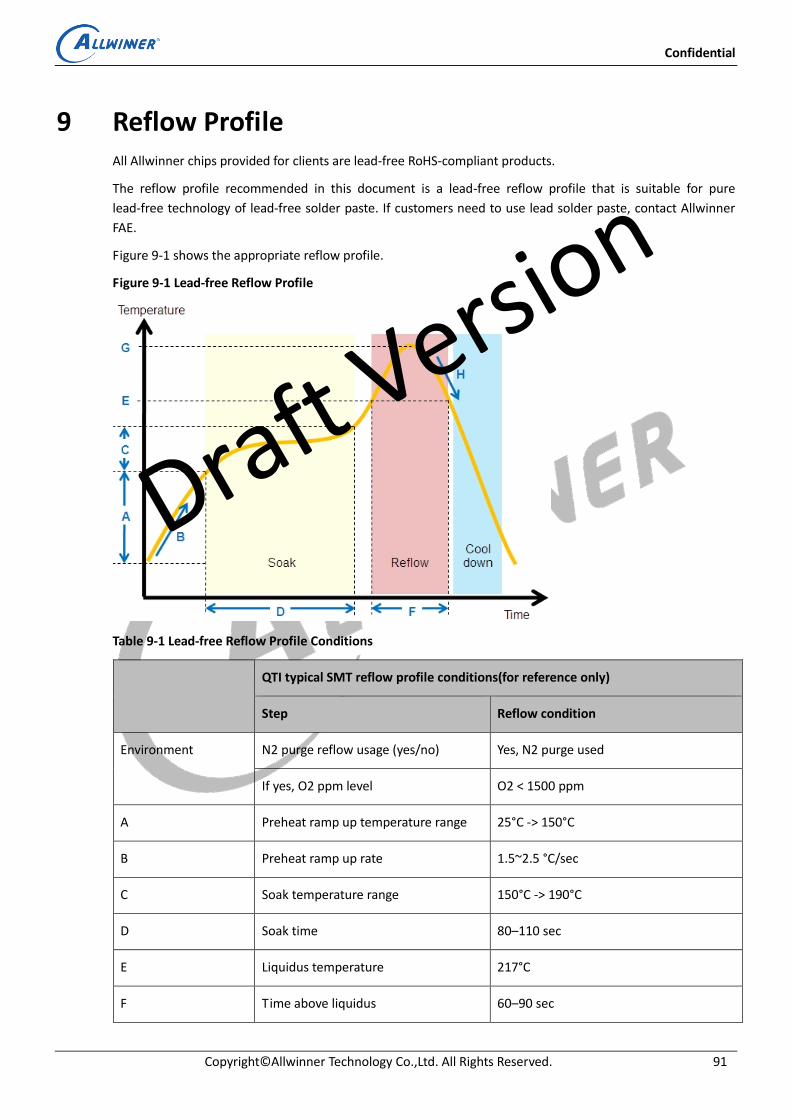
Confidential
Copyright© Allwinner Technology Co.,Ltd. All Rights Reserved. 91
9 Reflow Profile All Allwinner chips provided for clients are lead-free RoHS-compliant products.
The reflow profile recommended in this document is a lead-free reflow profile that is suitable for pure
lead-free technology of lead-free solder paste. If customers need to use lead solder paste, contact Allwinner
FAE.
Figure 9-1 shows the appropriate reflow profile.
Figure 9-1 Lead-free Reflow Profile
Table 9-1 Lead-free Reflow Profile Conditions
QTI typical SMT reflow profile conditions(for reference only)
Step Reflow condition
Environment N2 purge reflow usage (yes/no) Yes, N2 purge used
If yes, O2 ppm level O2 < 1500 ppm
A Preheat ramp up temperature range 25°C -> 150°C
B Preheat ramp up rate 1.5~2.5 °C/sec
C Soak temperature range 150°C -> 190°C
D Soak time 80–110 sec
E Liquidus temperature 217°C
F Time above liquidus 60–90 sec
Draft Versio
n
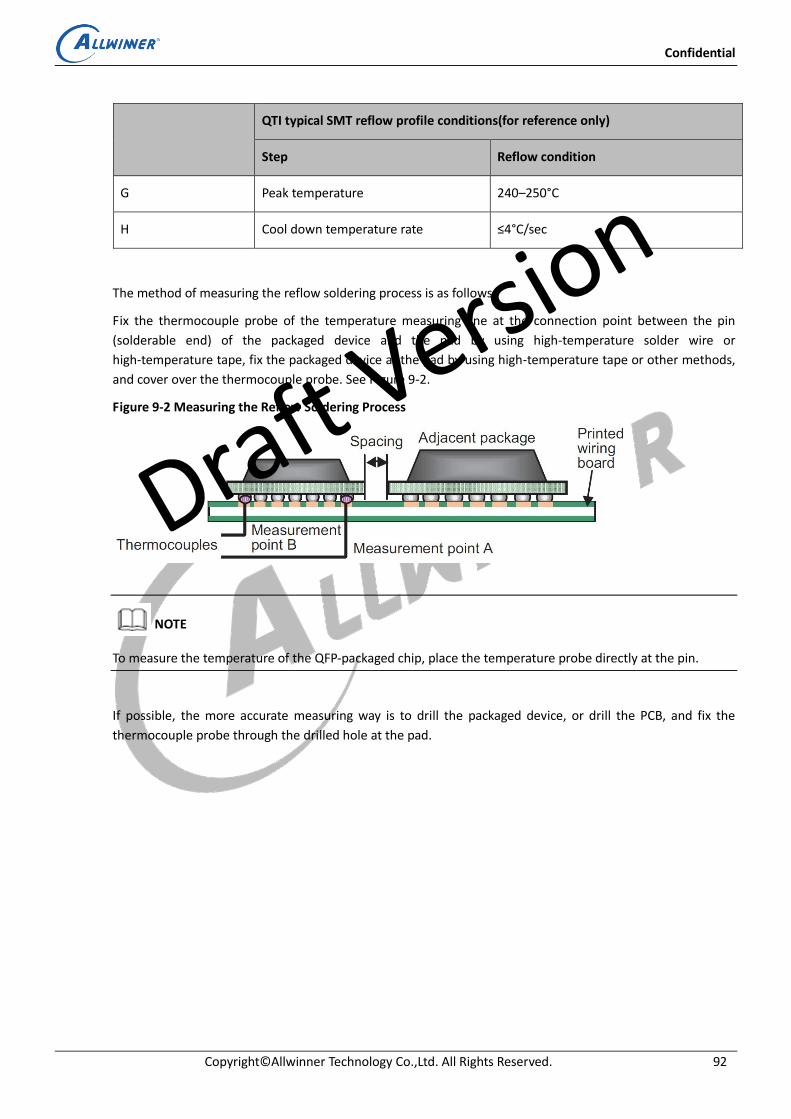
Confidential
Copyright© Allwinner Technology Co.,Ltd. All Rights Reserved. 92
QTI typical SMT reflow profile conditions(for reference only)
Step Reflow condition
G Peak temperature 240–250°C
H Cool down temperature rate ≤4°C/sec
The method of measuring the reflow soldering process is as follows.
Fix the thermocouple probe of the temperature measuring line at the connection point between the pin
(solderable end) of the packaged device and the pad by using high-temperature solder wire or
high-temperature tape, fix the packaged device at the pad by using high-temperature tape or other methods,
and cover over the thermocouple probe. See Figure 9-2.
Figure 9-2 Measuring the Reflow Soldering Process
To measure the temperature of the QFP-packaged chip, place the temperature probe directly at the pin.
If possible, the more accurate measuring way is to drill the packaged device, or drill the PCB, and fix the
thermocouple probe through the drilled hole at the pad.
NOTE
Draft Versio
n
Confidential
Copyright© Allwinner Technology Co.,Ltd. All Rights Reserved. 93
10 FT/QA/QC Test
10.1 FT Test
FT test is the finished product testing after the chip is packaged, and it is a functional test of all modules for
each produced chip.
10.2 QA Test
QA test is a system-level sampling test for good-quality chips. According to the application level of the chip, a
certain percentage of good-quality chips are selected for system-level testing to make the chip work in a
typical application scenario, and judge whether the chip works normally in this scenario.
10.3 QC Test
QC test is a module-level sampling test for good-quality chips. According to the chip application level, a
certain percentage of good-quality chips are selected for module-level functional testing to monitor whether
the chip production process is normal.
Draft Versio
n
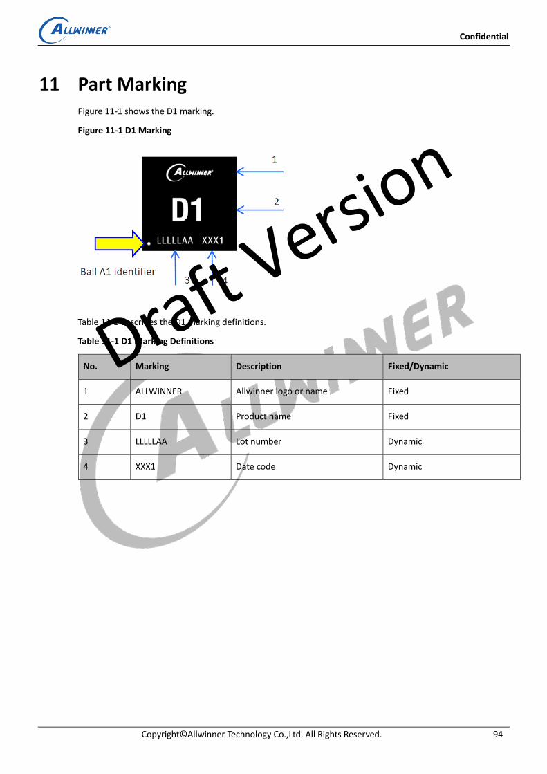
Confidential
Copyright© Allwinner Technology Co.,Ltd. All Rights Reserved. 94
11 Part Marking Figure 11-1 shows the D1 marking.
Figure 11-1 D1 Marking
Table 11-1 describes the D1 marking definitions.
Table 11-1 D1 Marking Definitions
No. Marking Description Fixed/Dynamic
1 ALLWINNER Allwinner logo or name Fixed
2 D1 Product name Fixed
3 LLLLLAA Lot number Dynamic
4 XXX1 Date code Dynamic
Draft Versio
n
Copyright© Allwinner Technology Co.,Ltd. All Rights Reserved. 95
Copyright© 2021 Allwinner Technology Co.,Ltd. All Rights Reserved.
This documentation is the original work and copyrighted property of Allwinner Technology Co.,Ltd (“Allwinner”). No
part of this document may be reproduced, modify, publish or transmitted in any form or by any means without prior
written consent of Allwinner.
Trademarks and Permissions
Allwinner and the Allwinner logo (incomplete enumeration) are trademarks of Allwinner Technology Co.,Ltd. All other
trademarks, trade names, product or service names mentioned in this document are the property of their respective
owners.
Important Notice and Disclaimer
The purchased products, services and features are stipulated by the contract made between Allwinner Technology
Co.,Ltd (“Allwinner”) and the customer. All or part of the products, services and features described in this document
may not be within the purchase scope or the usage scope. Please read the terms and conditions of the contract and
relevant instructions carefully before using, and follow the instructions in this documentation strictly. Allwinner
assumes no responsibility for the consequences of improper use (including but not limited to overvoltage, overclock, or
excessive temperature).
The information in this document is provided just as a reference or typical applications, and is subject to change
without notice. Every effort has been made in the preparation of this document to ensure accuracy of the contents.
Allwinner is not responsible for any damage (including but not limited to indirect, incidental or special loss) or any
infringement of third party rights arising from the use of this document. All statements, information, and
recommendations in this document do not constitute a warranty or commitment of any kind, express or implied.
No license is granted by Allwinner herein express or implied or otherwise to any patent or intellectual property of
Allwinner. Third party licences may be required to implement the solution/product. Customers shall be solely
responsible to obtain all appropriately required third party licences. Allwinner shall not be liable for any licence fee or
royalty due in respect of any required third party licence. Allwinner shall have no warranty, indemnity or other
obligations with respect to third party licences.
Draft Versio
n

Copyright© Allwinner Technology Co.,Ltd. All Rights Reserved. 96
Copyright © 2021 Allwinner Technology Co.,Ltd. All Rights Reserved.
Allwinner Technology Co.,Ltd.
No.9 Technology Road 2, High-Tech Zone,
Zhuhai, Guangdong Province, China
Contact US:
www.allwinnertech.com
Draft Versio
n