data sheet - futureelectronics.com technologies/hcms-3917… · data sheet. 2 package dimensions...
TRANSCRIPT
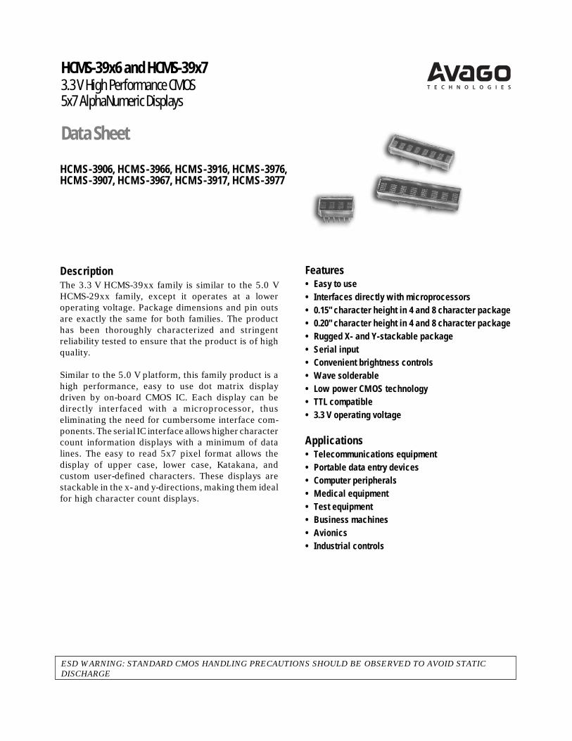
HCMS-3906, HCMS-3966, HCMS-3916, HCMS-3976,HCMS-3907, HCMS-3967, HCMS-3917, HCMS-3977
ESD WARNING: STANDARD CMOS HANDLING PRECAUTIONS SHOULD BE OBSERVED TO AVOID STATICDISCHARGE
DescriptionThe 3.3 V HCMS-39xx family is similar to the 5.0 VHCMS-29xx family, except it operates at a loweroperating voltage. Package dimensions and pin outsare exactly the same for both families. The producthas been thoroughly characterized and stringentreliability tested to ensure that the product is of highquality.
Similar to the 5.0 V platform, this family product is ahigh performance, easy to use dot matrix displaydriven by on-board CMOS IC. Each display can bedirectly interfaced with a microprocessor, thuseliminating the need for cumbersome interface com-ponents. The serial IC interface allows higher charactercount information displays with a minimum of datalines. The easy to read 5x7 pixel format allows thedisplay of upper case, lower case, Katakana, andcustom user-defined characters. These displays arestackable in the x- and y-directions, making them idealfor high character count displays.
Features• Easy to use• Interfaces directly with microprocessors• 0.15" character height in 4 and 8 character package• 0.20" character height in 4 and 8 character package• Rugged X- and Y-stackable package• Serial input• Convenient brightness controls• Wave solderable• Low power CMOS technology• TTL compatible• 3.3 V operating voltage
Applications• Telecommunications equipment• Portable data entry devices• Computer peripherals• Medical equipment• Test equipment• Business machines• Avionics• Industrial controls
HCMS-39x6 and HCMS-39x73.3 V High Performance CMOS5x7 AlphaNumeric Displays
Data Sheet
2
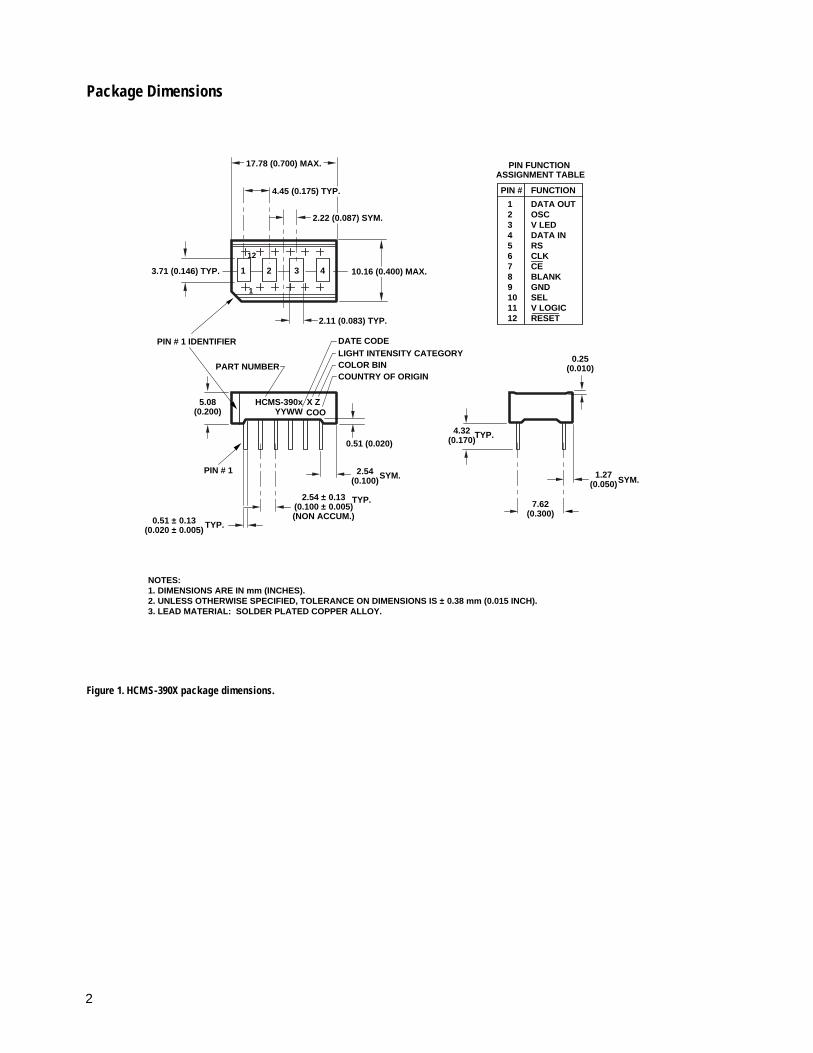
Package Dimensions
Figure 1. HCMS-390X package dimensions.
NOTES:1. DIMENSIONS ARE IN mm (INCHES).2. UNLESS OTHERWISE SPECIFIED, TOLERANCE ON DIMENSIONS IS ± 0.38 mm (0.015 INCH).3. LEAD MATERIAL: SOLDER PLATED COPPER ALLOY.
X ZCOO
2.11 (0.083) TYP.
0.25(0.010)
7.62(0.300)
PIN # 1 IDENTIFIER
4321
17.78 (0.700) MAX.
3.71 (0.146) TYP.
4.45 (0.175) TYP.
2.22 (0.087) SYM.
10.16 (0.400) MAX.
PIN # 1
LIGHT INTENSITY CATEGORYDATE CODE
COLOR BINCOUNTRY OF ORIGIN
PART NUMBER
5.08(0.200)
2.54(0.100)
SYM.
TYP.0.51 ± 0.13(0.020 ± 0.005)
2.54 ± 0.13(0.100 ± 0.005)(NON ACCUM.)
TYP.
4.32(0.170)
TYP.
1.27(0.050)SYM.
1
12
0.51 (0.020)
DATA OUTOSCV LEDDATA INRSCLKCEBLANKGNDSELV LOGICRESET
PIN FUNCTION ASSIGNMENT TABLE
123456789101112
PIN # FUNCTION
HCMS-390xYYWW
3
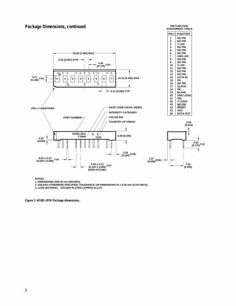
Figure 2. HCMS-391X Package dimensions.
NOTES:1. DIMENSIONS ARE IN mm (INCHES).2. UNLESS OTHERWISE SPECIFIED, TOLERANCE ON DIMENSIONS IS ± 0.38 mm (0.015 INCH).3. LEAD MATERIAL: SOLDER PLATED COPPER ALLOY.
2.54 ± 0.13(0.100 ± 0.005)(NON ACCUM.)
TYP.
35.56 (1.400) MAX.
76543210
0.25(0.010)
7.62(0.300)
PIN # 1 IDENTIFIER
X ZCOO
INTENSITY CATEGORY
DATE CODE (YEAR, WEEK)
COLOR BIN
COUNTRY OF ORIGIN
PART NUMBER
5.08 (0.200)
2.54(0.100) SYM.
0.51(0.020)
TYP.0.51 ± 0.13
(0.020 ± 0.005)
2.22 (0.087) SYM.
10.16 (0.400) MAX.
2.11 (0.083) TYP.
4.32(0.170)TYP.
1.27(0.050)SYM.
4.45 (0.175)TYP.
3.71 (0.146) TYP.
NO PINNO PINV LEDNO PINNO PINNO PINGND LEDNO PINNO PINV LEDNO PINNO PINNO PINDATA INRSNO PINCLOCKCEBLANKGND LOGICSELV LOGICNO PINRESETOSCDATA OUT
PIN FUNCTION ASSIGNMENT TABLE
1234567891011121314151617181920212223242526
PIN # FUNCTION
3
26
HCMS-391xYYWW
Package Dimensions, continued

4
Figure 3. HCMS-396X Package dimensions.
Package Dimensions, continued
NOTES:1. DIMENSIONS ARE IN mm (INCHES).2. UNLESS OTHERWISE SPECIFIED, THE TOLERANCE ON DIMENSIONS IS ± 0.38 mm (0.015 INCH).3. LEAD MATERIAL: SOLDER PLATED COPPER ALLOY.
3210
PIN # 1 IDENTIFIER
PART NUMBER
5.31(0.209)
0.169(4.28) SYM.
TYP.0.51 ± 0.13
(0.020 ± 0.005)
2.54 ± 0.13(0.100 ± 0.005)
TYP.
2.67 (0.105) SYM.
2.54 (0.100) TYP.
11.43 (0.450) MAX.
5.36 (0.211) TYP.
0.25(0.010)
7.62(0.300)
3.71(0.146)TYP.
0.072(1.83)SYM.
4.57 (0.180)TYP.
X ZCOO
INTENSITY CATEGORYDATE CODE (YEAR, WEEK)
COLOR BINCOUNTRY OF ORIGIN
21.46 (0.845) MAX.
0.50(0.020)
DATA OUTOSCV LEDDATA INRSCLKCEBLANKGNDSELV LOGICRESET
123456789101112
PIN FUNCTION ASSIGNMENT TABLE
PIN # FUNCTION
HCMS-396xYYWW

5
Figure 4. HCMS-397X Package dimensions.
Package Dimensions, continuedPIN FUNCTION
ASSIGNMENT TABLE
NOTES:1. DIMENSIONS ARE IN mm (INCHES).2. UNLESS OTHERWISE SPECIFIED, TOLERANCE ON DIMENSIONS IS ± 0.38 mm (0.015 INCH).3. LEAD MATERIAL: SOLDER PLATED COPPER ALLOY.
87654321
X ZCOO
PIN # 1 IDENTIFIER
INTENSITY CATEGORYDATE CODE (YEAR, WEEK)
COLOR BINCOUNTRY OF ORIGIN
PART NUMBER
5.31(0.209)
6.22(0.245) SYM.
0.51(0.020)
TYP.0.51 ± 0.13
(0.020 ± 0.005)
2.54 ± 0.13(0.100 ± 0.005)(NON ACCUM.)
TYP.
42.93 (1.690) MAX.
2.67 (0.105) SYM.
5.36 (0.211) TYP.
11.43 (0.450) MAX.
2.54 (0.100) TYP.
0.25(0.010)
7.62(0.300)
3.71(0.146)TYP.
1.90(0.075)SYM.
NO PINNO PINV LEDNO PINNO PINNO PINGND LEDNO PINNO PINV LEDNO PINNO PINNO PINDATA INRSNO PINCLOCKCEBLANKGND LOGICSELV LOGICNO PINRESETOSCDATA OUT
1234567891011121314151617181920212223242526
PIN # FUNCTION
4.57 (0.180)TYP.
3
26
HCMS-397xYYWW
6
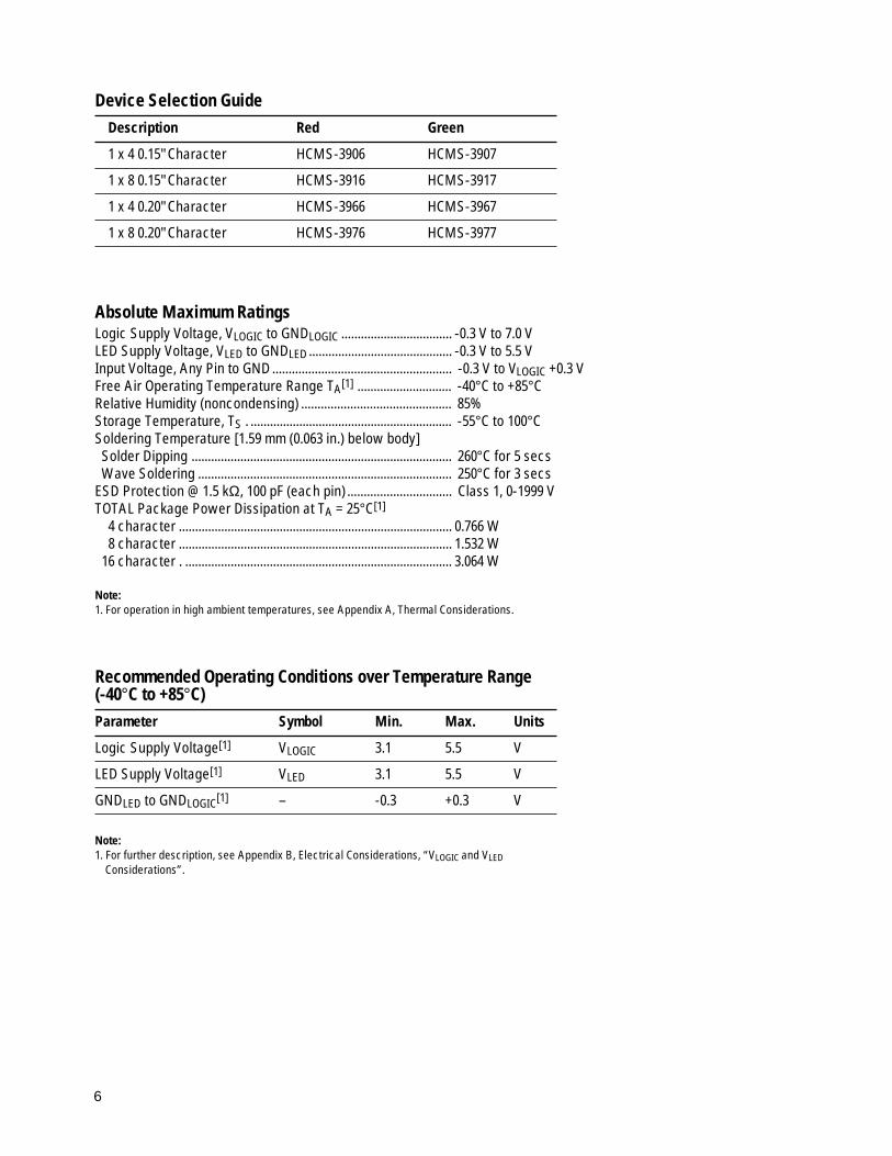
Device Selection GuideDescription Red Green
1 x 4 0.15" Character HCMS-3906 HCMS-3907
1 x 8 0.15" Character HCMS-3916 HCMS-3917
1 x 4 0.20" Character HCMS-3966 HCMS-3967
1 x 8 0.20" Character HCMS-3976 HCMS-3977
Absolute Maximum RatingsLogic Supply Voltage, VLOGIC to GNDLOGIC .................................. -0.3 V to 7.0 VLED Supply Voltage, VLED to GNDLED ............................................ -0.3 V to 5.5 VInput Voltage, Any Pin to GND ....................................................... -0.3 V to VLOGIC +0.3 VFree Air Operating Temperature Range TA[1] ............................. -40°C to +85°CRelative Humidity (noncondensing) .............................................. 85%Storage Temperature, TS . .............................................................. -55°C to 100°CSoldering Temperature [1.59 mm (0.063 in.) below body] Solder Dipping ................................................................................ 260°C for 5 secs Wave Soldering .............................................................................. 250°C for 3 secsESD Protection @ 1.5 kΩ, 100 pF (each pin) ................................ Class 1, 0-1999 VTOTAL Package Power Dissipation at TA = 25°C[1]
4 character .................................................................................... 0.766 W 8 character .................................................................................... 1.532 W 16 character . .................................................................................. 3.064 W
Note:1. For operation in high ambient temperatures, see Appendix A, Thermal Considerations.
Recommended Operating Conditions over Temperature Range(-40°C to +85°C)Parameter Symbol Min. Max. Units
Logic Supply Voltage[1] VLOGIC 3.1 5.5 V
LED Supply Voltage[1] VLED 3.1 5.5 V
GNDLED to GNDLOGIC[1] – -0.3 +0.3 V
Note:1. For further description, see Appendix B, Electrical Considerations, “VLOGIC and VLED
Considerations”.
7
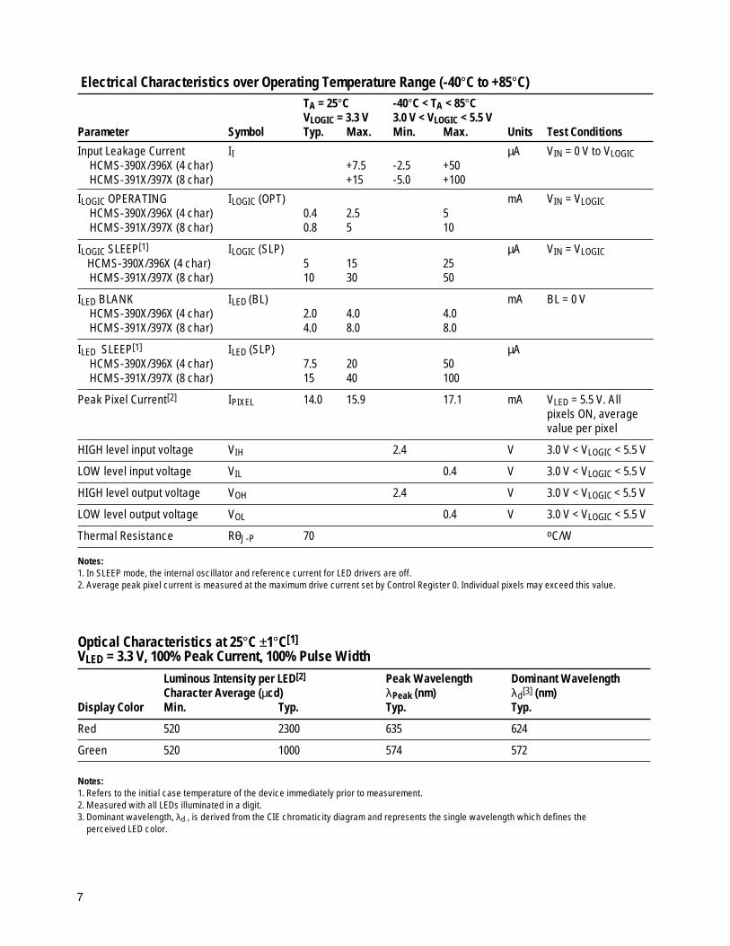
Electrical Characteristics over Operating Temperature Range (-40°C to +85°C)TA = 25°C -40°C < TA < 85°CVLOGIC = 3.3 V 3.0 V < VLOGIC < 5.5 V
Parameter Symbol Typ. Max. Min. Max. Units Test Conditions
Input Leakage Current II µA VIN = 0 V to VLOGICHCMS-390X/396X (4 char) +7.5 -2.5 +50HCMS-391X/397X (8 char) +15 -5.0 +100
ILOGIC OPERATING ILOGIC (OPT) mA VIN = VLOGICHCMS-390X/396X (4 char) 0.4 2.5 5HCMS-391X/397X (8 char) 0.8 5 10
ILOGIC SLEEP[1] ILOGIC (SLP) µA VIN = VLOGICHCMS-390X/396X (4 char) 5 15 25HCMS-391X/397X (8 char) 10 30 50
ILED BLANK ILED (BL) mA BL = 0 VHCMS-390X/396X (4 char) 2.0 4.0 4.0HCMS-391X/397X (8 char) 4.0 8.0 8.0
ILED SLEEP[1] ILED (SLP) µAHCMS-390X/396X (4 char) 7.5 20 50HCMS-391X/397X (8 char) 15 40 100
Peak Pixel Current[2] IPIXEL 14.0 15.9 17.1 mA VLED = 5.5 V. Allpixels ON, averagevalue per pixel
HIGH level input voltage VIH 2.4 V 3.0 V < VLOGIC < 5.5 V
LOW level input voltage VIL 0.4 V 3.0 V < VLOGIC < 5.5 V
HIGH level output voltage VOH 2.4 V 3.0 V < VLOGIC < 5.5 V
LOW level output voltage VOL 0.4 V 3.0 V < VLOGIC < 5.5 V
Thermal Resistance RθJ-P 70 oC/W
Notes:1. In SLEEP mode, the internal oscillator and reference current for LED drivers are off.2. Average peak pixel current is measured at the maximum drive current set by Control Register 0. Individual pixels may exceed this value.
Optical Characteristics at 25°C ±1°C[1]
VLED = 3.3 V, 100% Peak Current, 100% Pulse WidthLuminous Intensity per LED[2] Peak Wavelength Dominant WavelengthCharacter Average (µcd) λPeak (nm) λd[3] (nm)
Display Color Min. Typ. Typ. Typ.
Red 520 2300 635 624
Green 520 1000 574 572
Notes:1. Refers to the initial case temperature of the device immediately prior to measurement.2. Measured with all LEDs illuminated in a digit.3. Dominant wavelength, λd , is derived from the CIE chromaticity diagram and represents the single wavelength which defines the perceived LED color.

8
Electrical DescriptionPin Function Description
RESET (RST) Sets Control Register bits to logic low. The Dot Register contents areunaffected by the Reset pin. (logic low = reset; logic high = normaloperation).
DATA IN (DIN) Serial Data input for Dot or Control Register data. Data is entered on therising edge of the Clock input.
DATA OUT (DOUT) Serial Data output for Dot or Control Register data. This pin is used forcascading multiple displays.
CLOCK (CLK) Clock input for writing Dot or Control Register data. When Chip Enable islogic low, data is entered on the rising Clock edge.
REGISTER SELECT (RS) Selects Dot Register (RS = logic low) or Control Register (RS = logic high)as the destination for serial data entry. The logic level of RS is latched onthe falling edge of the Chip Enable input.
CHIP ENABLE (CE) This input must be a logic low to write data to the display. When CE returnsto logic high and CLK is logic low, data is latched to either the LED outputdrivers or a Control Register.
OSCILLATOR SELECT Selects either an internal or external display oscillator source. (SEL) (logiclow = External Display Oscillator; logic high = Internal Display Oscillator).
OSCILLATOR (OSC) Output for the Internal Display Oscillator (SEL = logic high) or input for anExternal Display Oscillator (SEL = logic low).
BLANK (BL) Blanks the display when logic high. May be modulated for brightnesscontrol.
GNDLED Ground for LED drivers.
GNDLOGIC Ground for logic.
VLED Positive supply for LED drivers.
VLOGIC Positive supply for logic.
9
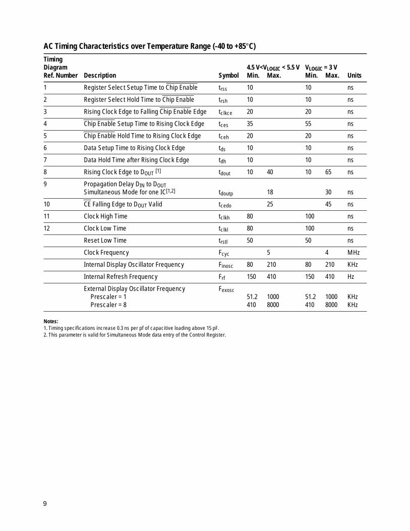
AC Timing Characteristics over Temperature Range (-40 to +85°C)
TimingDiagram 4.5 V<VLOGIC < 5.5 V VLOGIC = 3 VRef. Number Description Symbol Min. Max. Min. Max. Units
1 Register Select Setup Time to Chip Enable trss 10 10 ns
2 Register Select Hold Time to Chip Enable trsh 10 10 ns
3 Rising Clock Edge to Falling Chip Enable Edge tclkce 20 20 ns
4 Chip Enable Setup Time to Rising Clock Edge tces 35 55 ns
5 Chip Enable Hold Time to Rising Clock Edge tceh 20 20 ns
6 Data Setup Time to Rising Clock Edge tds 10 10 ns
7 Data Hold Time after Rising Clock Edge tdh 10 10 ns
8 Rising Clock Edge to DOUT [1] tdout 10 40 10 65 ns
9 Propagation Delay DIN to DOUTSimultaneous Mode for one IC[1,2] tdoutp 18 30 ns
10 CE Falling Edge to DOUT Valid tcedo 25 45 ns
11 Clock High Time tclkh 80 100 ns
12 Clock Low Time tclkl 80 100 ns
Reset Low Time trstl 50 50 ns
Clock Frequency Fcyc 5 4 MHz
Internal Display Oscillator Frequency Finosc 80 210 80 210 KHz
Internal Refresh Frequency Frf 150 410 150 410 Hz
External Display Oscillator Frequency FexoscPrescaler = 1 51.2 1000 51.2 1000 KHzPrescaler = 8 410 8000 410 8000 KHz
Notes:1. Timing specifications increase 0.3 ns per pf of capacitive loading above 15 pF.2. This parameter is valid for Simultaneous Mode data entry of the Control Register.

10
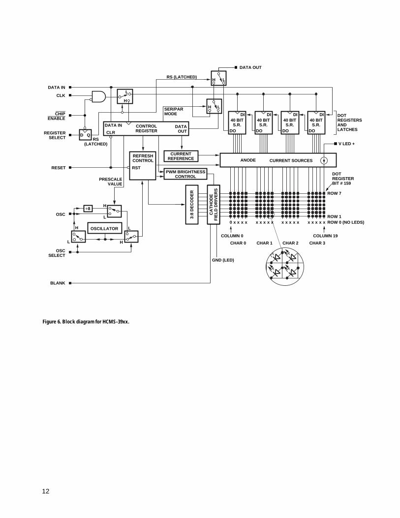
Display OverviewThe HCMS-39XX series is afamily of LED displays driven byon-board CMOS ICs. The LEDsare configured as 5x7 fontcharacters and are driven ingroups of 4 characters per IC.Each IC consists of a 160-bit shiftregister (the Dot Register), two7-bit Control Words, and refreshcircuitry. The Dot Registercontents are mapped on a one-to-one basis to the display. Thus, anindividual Dot Register bituniquely controls a single LED.
Eight-character displays have twoICs that are cascaded. The DataOut line of the first IC isinternally connected to the DataIn line of the second IC forming a320-bit Dot Register. Thedisplay’s other control and powerlines are connected directly toboth ICs.
ResetReset initializes the ControlRegisters (sets all ControlRegister bits to logic low) andplaces the display in the sleepmode. The Reset pin should beconnected to the system poweron reset circuit. The DotRegisters are not cleared uponpower-on or by Reset. Afterpower-on, the Dot Registercontents are random; however,Reset will put the display in sleepmode, thereby blanking theLEDs. The Control Register andthe Control Words are cleared toall zeros by Reset.
To operate the display after beingReset, load the Dot Register withlogic lows. Then load ControlWord 0 with the desiredbrightness level and set the sleepmode bit to logic high.
Dot RegisterThe Dot Register holds thepattern to be displayed by theLEDs. Data is loaded into the DotRegister according to theprocedure shown in Table 1 andFigure 5.
First RS is brought low, then CEis brought low. Next, eachsuccessive rising CLK edge willshift in the data at the DIN pin.Loading a logic high will turn thecorresponding LED on; a logiclow turns the LED off. When all160 bits have been loaded (or320 bits in an 8-digit display), CEis brought to logic high.
When CLK is next brought tologic low, new data is latched intothe display dot drivers. Loadingdata into the Dot Register takesplace while the previous data isdisplayed and eliminates the needto blank the display while loadingdata.
Table 1. Register Truth Table
Function CLK CE RS
Select Dot Register Not Rising ↓ L
Load Dot Register ↑ L XDIN = HIGH LED = “ON”DIN = LOW LED = “OFF”
Copy Data from Dot Register to Dot Latch L H X
Select Control Register Not Rising ↓ H
Load Control Register[1,3] ↑ L X
Latch Data to Control Word[2] L H X
Notes:1. BIT D0 of Control Word 1 must have been previously set to Low for serial mode or High for simultaneous mode.2. Selection of Control Word 1 or Control Word 0 is set by D7 of the Control Shift Register. The unselected control word retains its previous value.3. Control Word data is loaded Most Significant Bit (D7) first.

11
Figure 5. HCMS-39XX write cycle timing diagram.
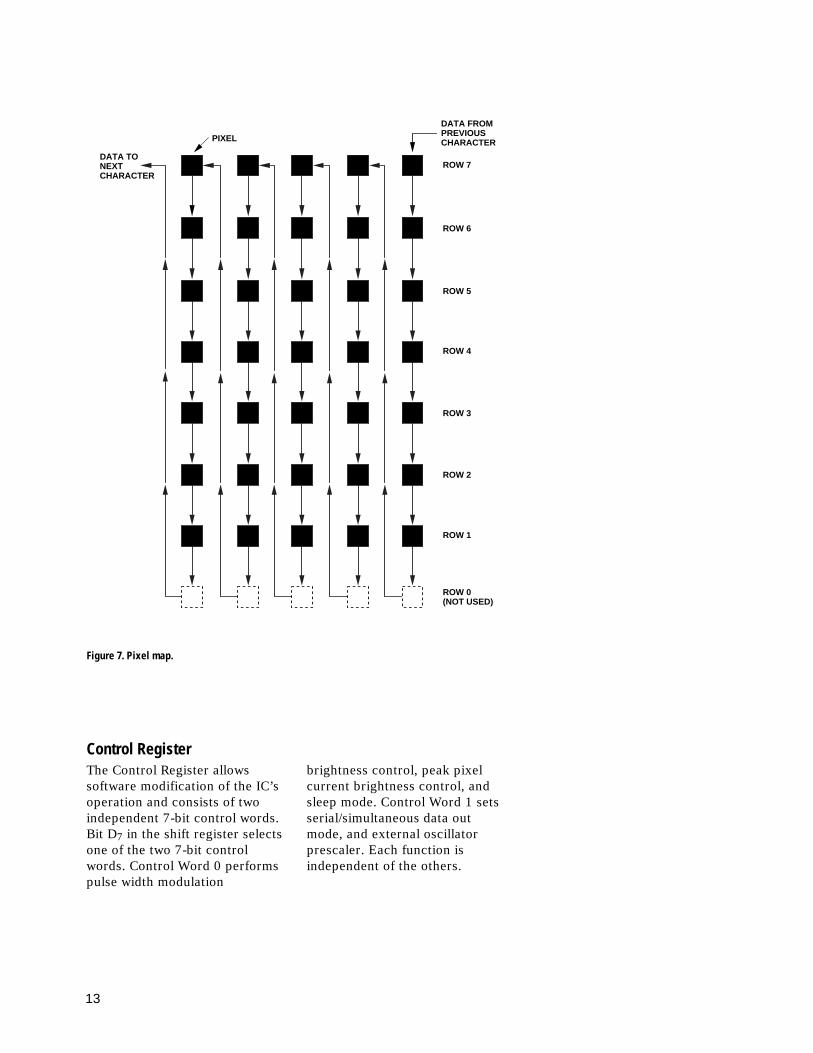
Pixel MapIn a 4-character display, the 160-bits are arranged as 20 columnsby 8 rows. This array can beconceptualized as four 5 x 8 dotmatrix character locations, butonly 7 of the 8 rows have LEDs(see Figures 6 & 7). The bottomrow (row 0) is not used. Thus,latch location 0 is neverdisplayed. Column 0 controls theleft-most column. Data from DotLatch locations 0-7 determinewhether or not pixels in Column
0 are turned-on or turned-off.Therefore, the lower left pixel isturned-on when a logic high isstored in Dot Latch location 1.Characters are loaded in serially,with the left-most characterbeing loaded first and the right-most character being loaded last.By loading one character at atime and latching the data beforeloading the next character, thefigures will appear to scroll fromright to left.
NOTE:1. DATA IS COPIED TO THE CONTROL REGISTER OR THE DOT LATCH AND LED OUTPUTS WHEN CE IS HIGH AND CLK IS LOW.
TRSS RSHT
TCLKCE CEST CLKHT CLKLT CEHT
DST DHT
CEDOT DOUTT
DOUTPT
PREVIOUS DATA NEW DATA
NEW DATA LATCHED HERE[1]
CE
RS
CLK
DIN
LED OUTPUTS,CONTROL
REGISTERS
DOUT(SIMULTANEOUS)
DOUT (SERIAL)
3 4
1 2
51211
6 7
10 8
9
12
Figure 6. Block diagram for HCMS-39xx.
40 BITS.R.
DO
DI
DATA IN
OSCILLATOR
÷8
CLK
CHIPENABLE
REGISTERSELECT
RESET
OSC
OSCSELECT
BLANK
DATA IN
CLRDATA
OUTCONTROLREGISTER
REFRESHCONTROL
RST
PRESCALEVALUE
H
L
H
L
L
H
D QRS
(LATCHED)
L
H
CURRENTREFERENCE
PWM BRIGHTNESSCONTROL
LH
LH
RS (LATCHED)
SER/PARMODE
3:8
DE
CO
DE
R
40 BITS.R.
DO
DI40 BITS.R.
DO
DI40 BITS.R.
DO
DI
ANODE CURRENT SOURCES
V LED +
GND (LED)
0
CHAR 0
COLUMN 0 COLUMN 19
CHAR 1 CHAR 2 CHAR 3
ROW 7
DOT REGISTERBIT # 159
ROW 1ROW 0 (NO LEDS)
DOTREGISTERSANDLATCHES
DATA OUT
CA
TH
OD
EF
IEL
D D
RIV
ER
S
x x x x x x x x x x x x x x x x x x x
13
Control RegisterThe Control Register allowssoftware modification of the IC’soperation and consists of twoindependent 7-bit control words.Bit D7 in the shift register selectsone of the two 7-bit controlwords. Control Word 0 performspulse width modulation
Figure 7. Pixel map.
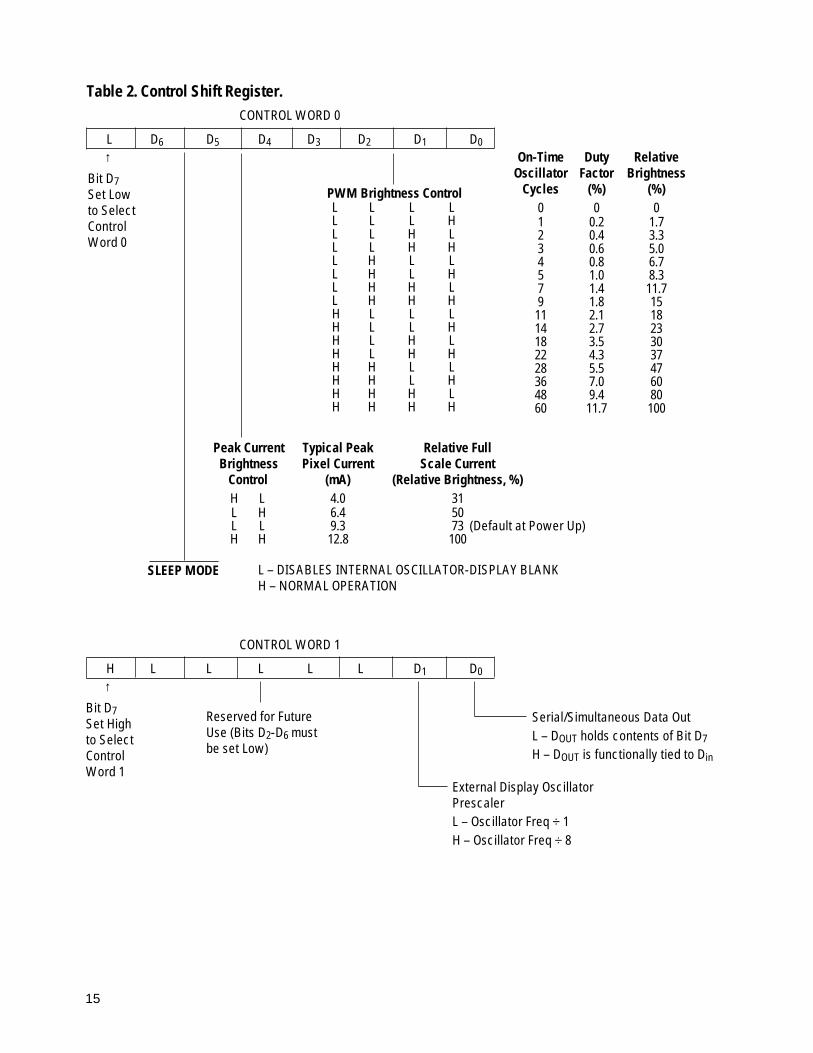
brightness control, peak pixelcurrent brightness control, andsleep mode. Control Word 1 setsserial/simultaneous data outmode, and external oscillatorprescaler. Each function isindependent of the others.
ROW 0 (NOT USED)
DATA TO NEXTCHARACTER
PIXEL
DATA FROMPREVIOUSCHARACTER
ROW 7
ROW 6
ROW 5
ROW 4
ROW 3
ROW 2
ROW 1

14
Control Register Data LoadingData is loaded into the ControlRegister, MSB first, according tothe procedure shown in Table 1and Figure 5. First, RS is broughtto logic high and then CE isbrought to logic low. Next, eachsuccessive rising CLK edge willshift in the data on the DIN pin.Finally, when 8 bits have beenloaded, the CE line is brought tologic high. When CLK goes tologic low, new data is copied intothe selected control word.Loading data into the ControlRegister takes place while theprevious control word configuresthe display.
Control Word 0Loading the Control Register withD7 = Logic low selects ControlWord 0 (see Table 2). Bits D0 -D3adjust the display brightness bypulse width modulating the LEDon time, while Bits D4 -D5 adjuststhe display brightness bychanging the peak pixel current.Bit D6 selects normal operationor sleep mode.
Sleep mode (Control Word 0, bitD6 = Low) turns off the InternalDisplay Oscillator and the LEDpixel drivers. This mode is usedwhen the IC needs to be poweredup, but does not need to be
active. Current draw in sleepmode is nearly zero. Data in theDot Register and Control Wordsare retained during sleep mode.
Control Word 1Loading the Control Register withD7 = logic high selects ControlWord 1. This Control Wordperforms two functions: serial/simultaneous data out mode andexternal oscillator prescale select(see Table 2).
15
Table 2. Control Shift Register.
L D6 D5 D4 D3 D2 D1 D0
Bit D7Set Lowto SelectControlWord 0
↑ On-Time Duty RelativeOscillator Factor Brightness
Cycles (%) (%)0 0 01 0.2 1.72 0.4 3.33 0.6 5.04 0.8 6.75 1.0 8.37 1.4 11.79 1.8 15
11 2.1 1814 2.7 2318 3.5 3022 4.3 3728 5.5 4736 7.0 6048 9.4 8060 11.7 100
PWM Brightness ControlL L L LL L L HL L H LL L H HL H L LL H L HL H H LL H H HH L L LH L L HH L H LH L H HH H L LH H L HH H H LH H H H
Peak Current Typical Peak Relative Full Brightness Pixel Current Scale Current Control (mA) (Relative Brightness, %)
H L 4.0 31L H 6.4 50L L 9.3 73 (Default at Power Up)H H 12.8 100
SLEEP MODE L – DISABLES INTERNAL OSCILLATOR-DISPLAY BLANKH – NORMAL OPERATION
CONTROL WORD 0
H L L L L L D1 D0↑
CONTROL WORD 1
Bit D7Set Highto SelectControlWord 1
Reserved for FutureUse (Bits D2-D6 mustbe set Low)
Serial/Simultaneous Data OutL – DOUT holds contents of Bit D7
H – DOUT is functionally tied to Din
External Display OscillatorPrescalerL – Oscillator Freq ÷ 1H – Oscillator Freq ÷ 8
16
Serial/Simultaneous DataOutput D0Bit D0 of control word 1 is usedto switch the mode of DOUTbetween serial and simultaneousdata entry during ControlRegister writes. The default mode(logic low) is the serial DOUTmode. In serial mode, DOUT isconnected to the last bit (D7) ofthe Control Shift Register.
Storing logic high to bit D0changes DOUT to simultaneousmode, which affects the ControlRegister only. In simultaneousmode, DOUT is logicallyconnected to DIN. This arrange-ment allows multiple ICs to havetheir Control Registers written tosimultaneously. For example, forn ICs in the serial mode, n * 8clock pulses are needed to loadthe same data in all ControlRegisters. In the simultaneousmode, n ICs only need 8 clockpulses to load the same data in allControl Registers. The propaga-tion delay from the first IC to thelast is n * tDOUTP.
External Oscillator PrescalerBit D1Bit D1 of Control Word 1 is usedto scale the frequency of anexternal Display Oscillator. When
this bit is logic low, the externalDisplay Oscillator directly setsthe internal display clock rate.When this bit is logic high, theexternal oscillator is divided by 8.This scaled frequency then setsthe internal display clock rate. Ittakes 512 cycles of the displayclock (or 8 x 512 = 4096 cyclesof an external clock with thedivide by 8 prescaler) tocompletely refresh the displayonce. Using the prescaler bitallows the designer to use ahigher external oscillatorfrequency without extra circuitry.
This bit has no affect on theinternal Display OscillatorFrequency.
Bits D2 -D6These bits must always beprogrammed to logic low.
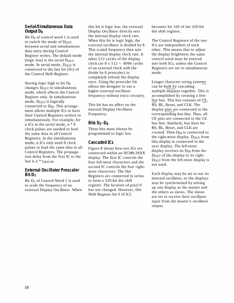
Cascaded ICsFigure 8 shows how two ICs areconnected within an HCMS-39XXdisplay. The first IC controls thefour left-most characters and thesecond IC controls the four right-most characters. The DotRegisters are connected in seriesto form a 320-bit dot shiftregister. The location of pixel 0has not changed. However, DotShift Register bit 0 of IC2
becomes bit 160 of the 320-bitdot shift register.
The Control Registers of the twoICs are independent of eachother. This means that to adjustthe display brightness the samecontrol word must be enteredinto both ICs, unless the ControlRegisters are set to simultaneousmode.
Longer character string systemscan be built by cascadingmultiple displays together. This isaccomplished by creating a five-line bus. This bus consists of CE,RS, BL, Reset, and CLK. Thedisplay pins are connected to thecorresponding bus line. Thus, allCE pins are connected to the CEbus line. Similarly, bus lines forRS, BL, Reset, and CLK arecreated. Then DIN is connected tothe right-most display. DOUT fromthis display is connected to thenext display. The left-mostdisplay receives its DIN from theDOUT of the display to its right.DOUT from the left-most display isnot used.
Each display may be set to use itsinternal oscillator, or the displaysmay be synchronized by settingup one display as the master andthe others as slaves. The slavesare set to receive their oscillatorinput from the master’s oscillatoroutput.
17
Figure 8. Cascaded ICs.
CE
IC2BITS 160-319
CHARACTERS 4-7
RS
BL
SEL
OSC
CLK
DOUT
DIN
IC1BITS 0-159
CHARACTERS 0-3DIN
RS
BL
SEL
OSC
CLK
DOUT
CE
RESET
RESET
RS
BL
SEL
OSC
CLK
DOUT
CE
RESET
DIN
18
Appendix A. ThermalConsiderations
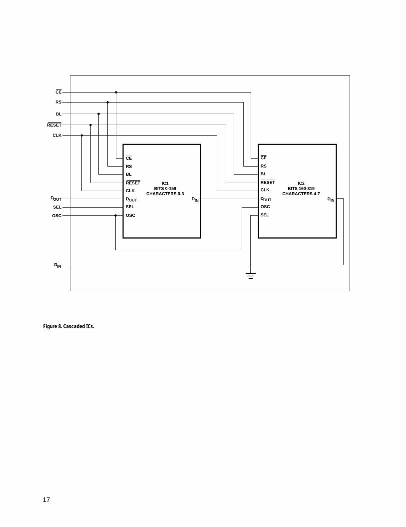
The display IC has a maximumjunction temperature of 150°C.The IC junction temperature canbe calculated with Equation 1 inTable 3.
A typical value for RθJA is 100°C/W. This value is typical for adisplay mounted in a socket andcovered with a plastic filter. Thesocket is soldered to a .062 inchthick PCB with .020-inch wide,
Figure 9. Maximum power dissipation per IC versus ambient temperature.
one ounce copper traces. PD canbe calculated as Equation 2 inTable 3.
Figure 9 shows how to derate thepower of one IC versus ambienttemperature. Operation at highambient temperatures mayrequire the power per IC to bereduced. The power consumptioncan be reduced by changing theN, IPIXEL , Osc cyc or VLED.Changing VLOGIC has very littleimpact on the powerconsumption.
P
MA
X –
MA
XIM
UM
PO
WE
R
DIS
SIP
AT
ION
PE
R IC
– W
D
025
TA– AMBIENT TEMPERATURE – °C
0.7
0.6
0.5
0.4
0.3
0.2
0.1
60555045403530
0.8
0.9
1.0
1.1
1.2
8580757065
R = 100°C/W
90
1.3θJ-A
19
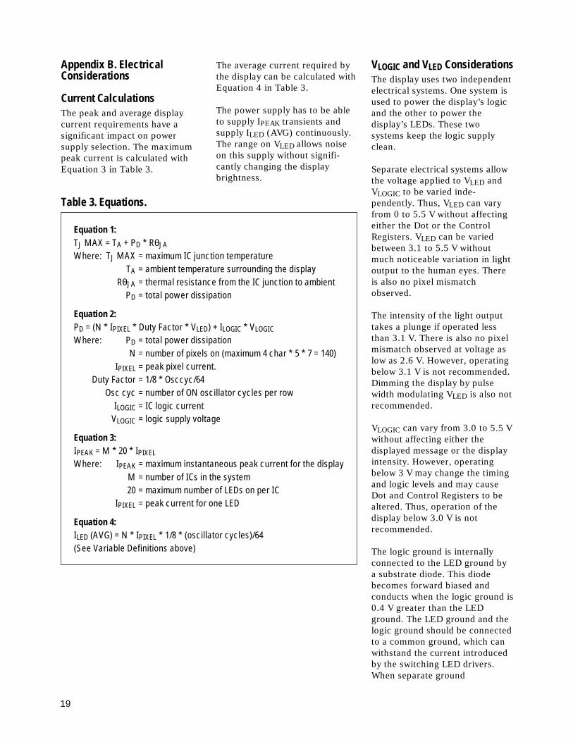
Appendix B. ElectricalConsiderations
Current CalculationsThe peak and average displaycurrent requirements have asignificant impact on powersupply selection. The maximumpeak current is calculated withEquation 3 in Table 3.
The average current required bythe display can be calculated withEquation 4 in Table 3.
The power supply has to be ableto supply IPEAK transients andsupply ILED (AVG) continuously.The range on VLED allows noiseon this supply without signifi-cantly changing the displaybrightness.
Table 3. Equations.
Equation 1:TJ MAX = TA + PD * RθJA
Where: TJ MAX = maximum IC junction temperatureTA = ambient temperature surrounding the display
RθJA = thermal resistance from the IC junction to ambientPD = total power dissipation
Equation 2:PD = (N * IPIXEL * Duty Factor * VLED) + ILOGIC * VLOGIC
Where: PD = total power dissipationN = number of pixels on (maximum 4 char * 5 * 7 = 140)
IPIXEL = peak pixel current.Duty Factor = 1/8 * Osccyc/64
Osc cyc = number of ON oscillator cycles per rowILOGIC = IC logic current
VLOGIC = logic supply voltage
Equation 3:IPEAK = M * 20 * IPIXEL
Where: IPEAK = maximum instantaneous peak current for the displayM = number of ICs in the system20 = maximum number of LEDs on per IC
IPIXEL = peak current for one LED
Equation 4:ILED (AVG) = N * IPIXEL * 1/8 * (oscillator cycles)/64(See Variable Definitions above)
VLOGIC and VLED ConsiderationsThe display uses two independentelectrical systems. One system isused to power the display’s logicand the other to power thedisplay’s LEDs. These twosystems keep the logic supplyclean.
Separate electrical systems allowthe voltage applied to VLED andVLOGIC to be varied inde-pendently. Thus, VLED can varyfrom 0 to 5.5 V without affectingeither the Dot or the ControlRegisters. VLED can be variedbetween 3.1 to 5.5 V withoutmuch noticeable variation in lightoutput to the human eyes. Thereis also no pixel mismatchobserved.
The intensity of the light outputtakes a plunge if operated lessthan 3.1 V. There is also no pixelmismatch observed at voltage aslow as 2.6 V. However, operatingbelow 3.1 V is not recommended.Dimming the display by pulsewidth modulating VLED is also notrecommended.
VLOGIC can vary from 3.0 to 5.5 Vwithout affecting either thedisplayed message or the displayintensity. However, operatingbelow 3 V may change the timingand logic levels and may causeDot and Control Registers to bealtered. Thus, operation of thedisplay below 3.0 V is notrecommended.
The logic ground is internallyconnected to the LED ground bya substrate diode. This diodebecomes forward biased andconducts when the logic ground is0.4 V greater than the LEDground. The LED ground and thelogic ground should be connectedto a common ground, which canwithstand the current introducedby the switching LED drivers.When separate ground

Appendix D. Refresh Circuitry
This display driver consists of 20one-of-eight column decoders and20 constant current sources, 1one-of-eight row decoder andeight row sinks, a pulse widthmodulation control block, a peakcurrent control block, and thecircuit to refresh the LEDs. Therefresh counters and oscillatorare used to synchronize thecolumns and rows.
The 160 bits are organized as 20columns by 8 rows. The ICilluminates the display bysequentially turning ON each ofthe 8 row-drivers. To refresh thedisplay once takes 512 oscillatorcycles. Because there are eightrow drivers, each row driver isselected for 64 (512/8) oscillatorcycles. Four cycles are used tobriefly blank the display beforethe following row is switched on.Thus, each row is ON for 60oscillator cycles out of a possible64. This corresponds to themaximum LED on time.
The temperature of the displaywill also affect the LED bright-ness as shown in Figure 10.
connections are used, the LEDground can vary from -0.3 V to+0.3 V with respect to the logicground. Voltages below -0.3 V cancause all the dots to be ON.Voltage above +0.3 V can causedimming and dot mismatch.
Using a decoupling capacitorbetween the power supply andground will help prevent anysupply noise in the frequencyrange greater than that of thefunctioning display frominterfering with the display’sinternal circuitry. The value of thecapacitor depends on the seriesresistance from the ground backto the power supply and the rangeof frequencies that need to besuppressed. It is alsoadvantageous to use the largestground plane possible.
Electrostatic DischargeThe inputs to the ICs areprotected against static dischargeand input current latch up.However, for best results,standard CMOS handlingprecautions should be used.Before use, the HCMS-39XXshould be stored in antistatictubes or in conductive material.During assembly, a groundedconductive work area should beused and assembly personnelshould wear conductive wriststraps. Lab coats made ofsynthetic material should beavoided since they are prone tostatic buildup. Input current latchup is caused when the CMOSinputs are subjected to either avoltage below ground(VIN < ground) or to a voltagehigher than VLOGIC (VIN > VLOGIC)and when a high current is forcedinto the input. To prevent inputcurrent latch up and ESD damage,unused inputs should beconnected to either ground orVLOGIC. Voltages should not beapplied to the inputs until VLOGIChas been applied to the display.
Appendix C. Oscillator
The oscillator provides theinternal refresh circuitry with asignal that is used to synchronizethe columns and rows. Thisensures that the right data is inthe dot drivers for that row. Thissignal can be supplied fromeither an external source or theinternal source.
A display refresh rate of 100 Hzor faster ensures flicker-freeoperation. Thus, for an externaloscillator the frequency should begreater than or equal to 512 x100 Hz = 51.2 kHz. Operationabove 1 MHz without theprescaler or 8 MHz with theprescaler may cause noticeablepixel-to-pixel mismatch.

Appendix F. ReferenceMaterial
Application Note 1027:Soldering LED Components
Application Note 1015: ContrastEnhancement Techniques forLED Displays
Figure 10. Relative luminous Intensity versus ambient temperature.
Appendix E. DisplayBrightness
Two ways have been shown tocontrol the brightness of thisLED display: setting the peakcurrent and setting the dutyfactor. Both values are set inControl Word 0. To compute theresulting display brightness whenboth PWM and peak currentcontrol are used, simply multiplythe two relative brightnessfactors. For example, if ControlRegister 0 holds the word
1001101, the peak current is73% of full scale (BIT D5=L, BITD4 = L) and the PWM is set to60% duty factor (BIT D3 = H,BIT D2 = H, BIT D1 = L, BIT D0= H). The resulting brightness is44% (.73 x .60 = .44) of fullscale.
The temperature of the displaywill also affect the LEDbrightness as shown in Figure 10.
RE
LA
TIV
E L
UM
INO
US
INT
EN
SIT
Y(N
OR
MA
LIZ
ED
TO
1 A
T 2
0°C
)
0-50
AMBIENT TEMPERATURE – °C
3.0
2.5
2.0
1.5
1.0
0.5
100500
RED
GREEN

For product information and a complete list of distributors, please go to our website: www.avagotech.com
Avago, Avago Technologies, and the A logo are trademarks of Avago Technologies, Limited in the United States and other countries.Data subject to change. Copyright © 2006 Avago Technologies Pte. All rights reserved. Obsoletes 5988-7528EN5989-3185EN May 27, 2006