datasheet for telink ble soc tlsr8232wiki.telink-semi.cn/doc/ds/ds_tlsr8232-e_datasheet... ·...
TRANSCRIPT
Datasheet for Telink
BLE SoC TLSR8232
DS-TLSR8232-E3
Ver 0.8.2
2020/4/10
2016/1/29
TE
LIN
K S
EM
ICO
ND
UC
TO
R
Keyword:
BLE; 2.4GHz; Features; Package; Pin layout; Memory;
MCU; Working modes; Wakeup sources; RF Transceiver;
Baseband; Clock; Timers; Interrupt; Interface; PWM;
QDEC; ADC; PGA; AES; Electrical specification
Brief:
This datasheet is dedicated for Telink BLE SoC TLSR8232.
In this datasheet, key features, working mode, main
modules, electrical specification and application of the
TLSR8232 are introduced.
Datasheet for Telink TLSR8232
DS-TLSR8232-E3 1 Ver0.8.2
Published by
Telink Semiconductor
Bldg 3, 1500 Zuchongzhi Rd,
Zhangjiang Hi-Tech Park, Shanghai, China
© Telink Semiconductor
All Right Reserved
Legal Disclaimer
Telink Semiconductor reserves the right to make changes without further notice to
any products herein to improve reliability, function or design. Telink Semiconductor
disclaims any and all liability for any errors, inaccuracies or incompleteness contained
herein or in any other disclosure relating to any product.
Telink Semiconductor does not assume any liability arising out of the application or
use of any product or circuit described herein; neither does it convey any license
under its patent rights, nor the rights of others
The products shown herein are not designed for use in medical, life-saving, or
life-sustaining applications. Customers using or selling Telink Semiconductor products
not expressly indicated for use in such applications do so entirely at their own risk and
agree to fully indemnify Telink Semiconductor for any damages arising or resulting
from such use or sale.
Information:
For further information on the technology, product and business term, please contact
Telink Semiconductor Company (www.telink-semi.com).
For sales or technical support, please send email to the address of:
Datasheet for Telink TLSR8232
DS-TLSR8232-E3 2 Ver0.8.2
Revision History
Version Major Changes Date Author
0.8.0 Preliminary release 2017/12
M.Z.D., Y.C.Q.,
S.G.J., L.W.F., J.H.P.,
X.X., X.S.J., Cynthia
0.8.1
Updated the following sections:
5.3 System Timer,
6.2 Register configuration and 9.7
Register table (removed QDEC interrupt
and System Timer interrupt),
7.1.1.1 GPIO lookup table (notes),
7.1.3 Pull-up/Pull-down resistor,
7.3.5 I2C and SPI Usage,
10 SAR ADC.
Added section 15 .
2018/2
M.Z.D., Y.C.Q.,
L.W.F., T.J.B.,
X.W.W., Cynthia
0.8.2
Updated the sections below:
10 SAR ADC,
12 Temperature Sensor,
15 Reference Design.
Modified Accuracy in
1.2.2
3.3.2
14.4
Modified Rx sensitivity and Tx power in
1.2.2
14.4
Modified receiver mode current in
1.2.3
2019/3 YCQ, LX, SY, LWF,
Cynthia, YH
Datasheet for Telink TLSR8232
DS-TLSR8232-E3 3 Ver0.8.2
1 Table of contents
1 Overview ................................................................................................................ 9
1.1 Block diagram ................................................................................................ 9
1.2 Key features ................................................................................................. 10
1.2.1 General features ..................................................................................... 10
1.2.2 RF Features ............................................................................................. 11
1.2.3 Features of power management module ............................................... 11
1.2.4 Flash features ......................................................................................... 11
1.3 Typical application ....................................................................................... 12
1.4 Ordering information .................................................................................. 12
1.5 Package ........................................................................................................ 12
1.6 Pin layout ..................................................................................................... 15
1.6.1 Pin layout for TLSR8232F512/F128ET32 ................................................ 15
1.6.2 Pin layout for TLSR8232F512/F128ET24 ................................................ 18
1.6.3 Notes ....................................................................................................... 20
2 Memory and MCU ................................................................................................ 21
2.1 Memory ....................................................................................................... 21
2.1.1 SRAM/Register ........................................................................................ 21
2.1.2 Flash ........................................................................................................ 21
2.2 Firmware encryption ................................................................................... 22
2.3 MCU ............................................................................................................. 22
2.4 Working modes............................................................................................ 23
2.4.1 Active mode ............................................................................................ 23
2.4.2 Idle mode ................................................................................................ 23
2.4.3 Power-saving mode ................................................................................ 23
2.5 Reset .............................................................................................................. 25
2.6 Power Management ...................................................................................... 26
2.6.1 Power-On-Reset (POR) and Brown-out detect ....................................... 26
2.6.2 Working mode switch ............................................................................. 29
2.6.3 LDO and DCDC ........................................................................................ 30
2.7 Wakeup sources ............................................................................................ 30
2.7.1 Wakeup source – 32K timer ................................................................... 31
2.7.2 Wakeup source – IO ............................................................................... 31
2.7.3 Register table .......................................................................................... 31
3 BLE/2.4G RF Transceiver ...................................................................................... 33
3.1 Block diagram .............................................................................................. 33
3.2 Function description .................................................................................... 33
3.2.1 Air interface data rate and RF channel frequency ................................. 33
3.3 Baseband ..................................................................................................... 33
3.3.1 Packet format ......................................................................................... 34
Datasheet for Telink TLSR8232
DS-TLSR8232-E3 4 Ver0.8.2
3.3.2 RSSI and frequency offset ....................................................................... 34
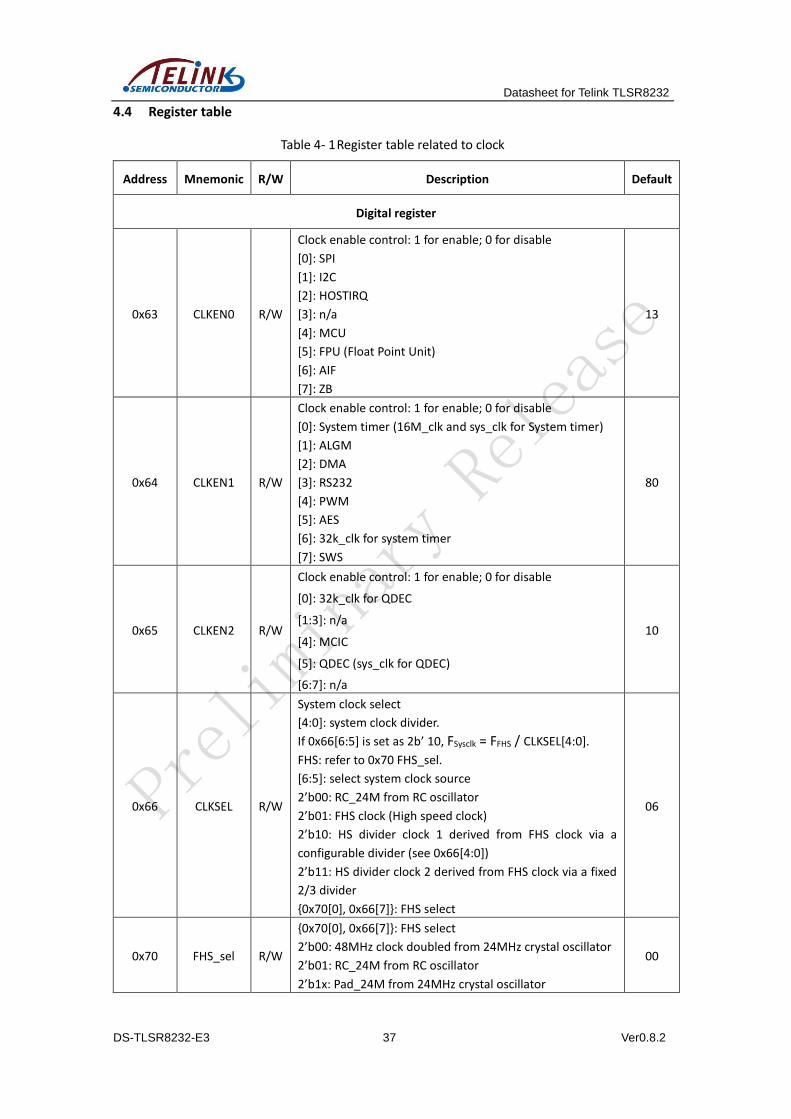
4 Clock ..................................................................................................................... 35
4.1 Clock sources ............................................................................................... 35
4.2 System clock ................................................................................................ 36
4.3 Module clock ............................................................................................... 36
4.3.1 System Timer clock ................................................................................. 36
4.3.2 QDEC clock .............................................................................................. 36
4.4 Register table ............................................................................................... 37
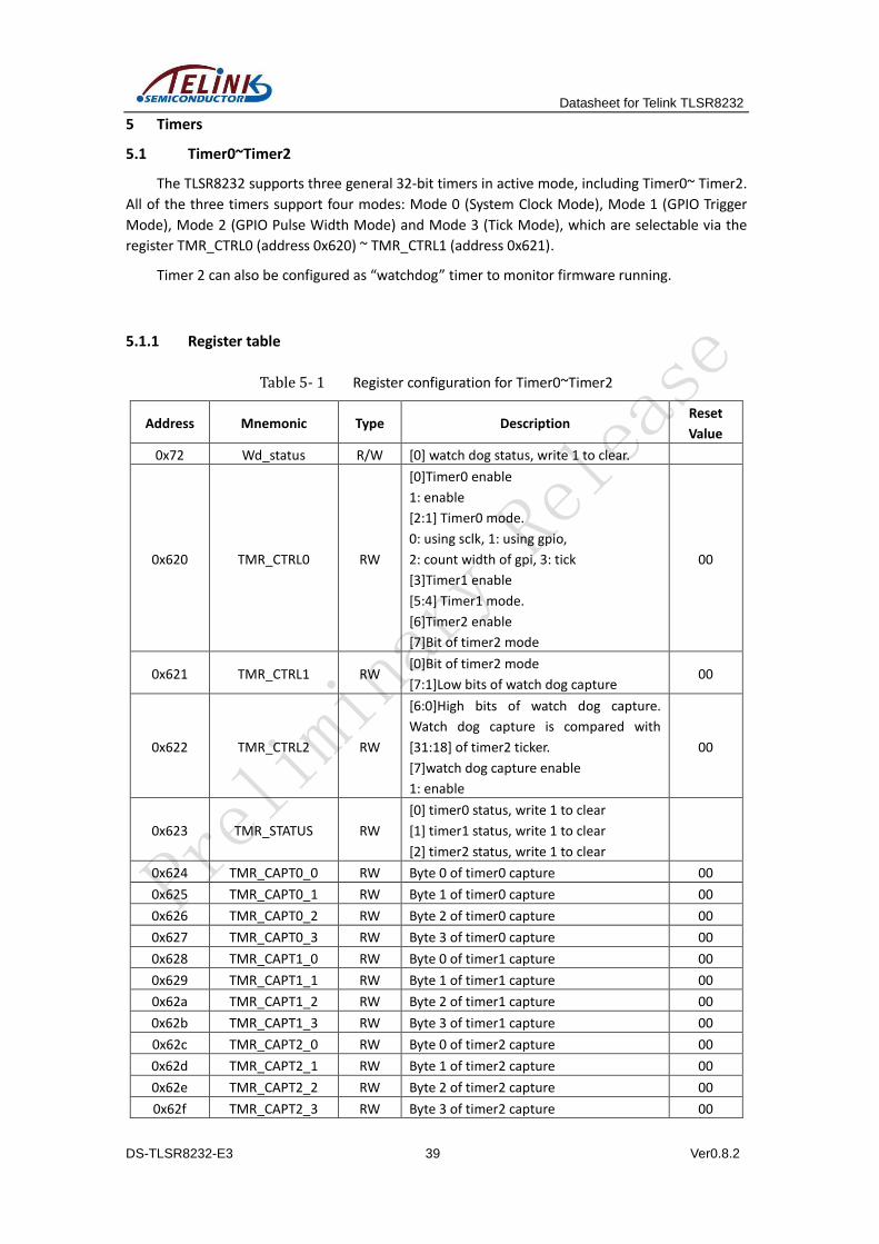
5 Timers ................................................................................................................... 39
5.1 Timer0~Timer2 ............................................................................................ 39
5.1.1 Register table .......................................................................................... 39
5.1.2 Mode0 (System Clock Mode) ................................................................. 40
5.1.3 Mode1 (GPIO Trigger Mode) .................................................................. 40
5.1.4 Mode2 (GPIO Pulse Width Mode) .......................................................... 41
5.1.5 Mode3 (Tick Mode) ................................................................................ 42
5.1.6 Watchdog ............................................................................................... 42
5.2 32kHz LTIMER .............................................................................................. 43
5.3 System Timer ............................................................................................... 43
6 Interrupt System .................................................................................................. 45
6.1 Interrupt structure ....................................................................................... 45
6.2 Register configuration ................................................................................. 45
6.2.1 Enable/Mask interrupt sources .............................................................. 46
6.2.2 Interrupt mode and priority ................................................................... 46
6.2.3 Interrupt source flag ............................................................................... 47
7 Interface ............................................................................................................... 48
7.1 GPIO ............................................................................................................. 48
7.1.1 Basic configuration ................................................................................. 48
7.1.1.1 GPIO lookup table .............................................................................. 48
7.1.1.2 Multiplexed functions ........................................................................ 51
7.1.1.3 Drive strength .................................................................................... 52
7.1.2 Connection relationship between GPIO and related modules .............. 52
7.1.3 Pull-up/Pull-down resistor ...................................................................... 55
7.2 SWS .............................................................................................................. 58
7.3 I2C ................................................................................................................ 58
7.3.1 Communication protocol ........................................................................ 58
7.3.2 Register table .......................................................................................... 59
7.3.3 I2C Slave mode ....................................................................................... 60
7.3.3.1 DMA mode ......................................................................................... 60
7.3.3.2 Mapping mode .................................................................................. 61
7.3.4 I2C Master mode .................................................................................... 61
7.3.4.1 I2C Master Write transfer ...................................................................... 62
7.3.4.2 I2C Master Read transfer ....................................................................... 62
Datasheet for Telink TLSR8232
DS-TLSR8232-E3 5 Ver0.8.2
7.3.5 I2C and SPI Usage ................................................................................... 62
7.4 SPI ................................................................................................................ 63
7.4.1 Register table .............................................................................................. 63
7.4.2 SPI Master mode ......................................................................................... 63
7.4.3 SPI Slave mode ............................................................................................ 64
7.4.4 I2C and SPI Usage ................................................................................... 65
7.5 UART ............................................................................................................ 66
8 PWM ..................................................................................................................... 69
8.1 Register table ................................................................................................. 69
8.2 Enable PWM .................................................................................................. 72
8.3 Set PWM clock ............................................................................................... 72
8.4 PWM waveform, polarity and output inversion ........................................... 72
8.4.1 Waveform of signal frame ...................................................................... 73
8.4.2 Invert PWM output ................................................................................. 73
8.4.3 Polarity for signal frame ......................................................................... 73
8.5 PWM mode .................................................................................................... 74
8.5.1 Select PWM mode .................................................................................. 74
8.5.2 Continuous mode ................................................................................... 74
8.5.3 Counting mode ....................................................................................... 75
8.5.4 IR mode ................................................................................................... 75
8.5.5 IR FIFO mode .......................................................................................... 76
8.5.6 IR DMA FIFO mode ................................................................................. 77
8.6 PWM interrupt............................................................................................... 81
9 Quadrature Decoder ............................................................................................ 82
9.1 Input pin selection ......................................................................................... 82
9.2 Common mode and double accuracy mode ................................................. 82
9.3 Read real time counting value ....................................................................... 84
9.4 QDEC reset ..................................................................................................... 85
9.5 Other configuration ....................................................................................... 85
9.6 Timing sequence ............................................................................................ 86
9.7 Register table ................................................................................................. 87
10 SAR ADC ................................................................................................................ 88
10.1 Power on/down ............................................................................................. 88
10.2 ADC clock ....................................................................................................... 88
10.3 ADC control in auto mode ............................................................................. 89
10.3.1 Set max state and enable channel.......................................................... 89
10.3.2 “Set” state ............................................................................................... 89
10.3.3 “Capture” state ....................................................................................... 90
10.3.4 Usage cases ............................................................................................. 91
10.3.4.1 Case 1: 4-channel sampling for random number, Left, Right and Misc
91
10.3.4.2 Case 2: 3-channel sampling for random number, Left and Misc ....... 91
Datasheet for Telink TLSR8232
DS-TLSR8232-E3 6 Ver0.8.2
10.3.4.3 Case 3: 3-channel sampling for Left, Right and Misc ......................... 92
10.3.4.4 Case 4: 3-channel sampling for random number, Left and Right ...... 92
10.3.4.5 Case 5: 2-channel sampling for Left and Misc ................................... 92
10.3.4.6 Case 6: 2-channel sampling for random number and Left ................ 93
10.3.4.7 Case 7: 2-channel sampling for random number and Misc............... 93
10.3.4.8 Case 8: 2-channel sampling for Left and Right .................................. 93
10.3.4.9 Case 9: 1-channel sampling for Left .................................................. 93
10.3.4.10 Case 10: 1-channel sampling for Misc ........................................ 94
10.3.4.11 Case 11: 1-channel sampling for RNG ........................................ 94
10.3.4.12 Case 12: RSSI capture ................................................................. 94
10.3.4.13 Case 13 with detailed register setting ........................................ 95
10.4 Register table ................................................................................................. 97
11 PGA ..................................................................................................................... 102
11.1 Power on/down ........................................................................................... 103
11.2 Select input channel .................................................................................... 103
11.3 Adjust gain ................................................................................................... 103
11.4 Enable/Disable PGA output ......................................................................... 103
11.5 Load digital register 0x3c ............................................................................. 103
11.6 Register table ............................................................................................... 104
12 Temperature Sensor ........................................................................................... 105
13 AES ...................................................................................................................... 107
13.1 RISC mode .................................................................................................... 107
13.2 AES-CCM ...................................................................................................... 107
13.3 Register table ............................................................................................... 108
14 Key Electrical Specifications ............................................................................... 109
14.1 Absolute maximum ratings .......................................................................... 109
14.2 Recommended operating condition ............................................................ 109
14.3 DC characteristics ........................................................................................ 110
14.4 AC characteristics ........................................................................................ 111
15 Reference Design ............................................................................................... 114
15.1 Application example .................................................................................... 114
15.1.1 Schematic ............................................................................................. 114
15.1.2 BOM (Bill of Material) ........................................................................... 115
Datasheet for Telink TLSR8232
DS-TLSR8232-E3 7 Ver0.8.2
2 Table of figures
Figure 1- 1 Block diagram of the system ................................................................ 9
Figure 1- 2 Package dimension for the TLSR8232F512/F128ET32 (Unit: mm) .... 13
Figure 1- 3 Package dimension for TLSR8232F512/F128ET24 (Unit: mm) .......... 14
Figure 1- 4 Pin assignment for TLSR8232F512/F128ET32 ................................... 15
Figure 1- 5 Pin assignment for TLSR8232F512/F128ET24 ................................... 18
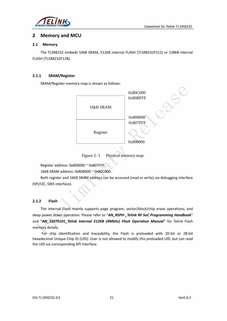
Figure 2- 1 Physical memory map ........................................................................ 21
Figure 2- 2 Transition chart of working modes .................................................... 23
Figure 2- 3 Block diagram for power up/down .................................................... 26
Figure 2- 4 Power-up sequence ........................................................................... 27
Figure 2- 5 Power-down sequence ...................................................................... 28
Figure 2- 6 Wakeup sources ................................................................................. 30
Figure 3- 1 Block diagram of RF transceiver ........................................................ 33
Figure 7- 1 Logic relationship between GPIO and related modules .................... 53
Figure 7- 2 I2C timing chart ................................................................................. 58
Figure 7- 3 Byte consisted of slave address and R/W flag bit .............................. 60
Figure 7- 4 Read format in DMA mode ................................................................ 60
Figure 7- 5 Write format in DMA mode ............................................................... 61
Figure 7- 6 Read format in Mapping mode.......................................................... 61
Figure 7- 7 Write format in Mapping mode ......................................................... 61
Figure 7- 8 SPI write/read command format ....................................................... 65
Figure 7- 9 UART communication ........................................................................ 66
Figure 8- 1 A signal frame .................................................................................... 73
Figure 8- 2 PWM output waveform chart ............................................................ 74
Figure 8-3 Continuous mode .............................................................................. 74
Figure 8-4 Counting mode (n=0) ......................................................................... 75
Figure 8-5 IR mode (n=0) .................................................................................... 76
Figure 8- 6 IR format examples ............................................................................ 77
Figure 9- 1 Common mode .................................................................................. 83
Figure 9- 2 Double accuracy mode ...................................................................... 84
Figure 9- 3 Read real time counting value ........................................................... 85
Figure 9- 4 Shuttle mode ..................................................................................... 85
Figure 9- 5 Timing sequence chart ...................................................................... 86
Figure 10- 1 Block diagram of ADC ........................................................................ 88
Figure 11- 1 Block diagram of PGA ...................................................................... 102
Figure 12- 1 Block diagram of temperature sensor ............................................. 105
Figure 15-1 Schematic for TLSR8232F512ET32 .................................................. 115
Figure 15-2 Layout for TLSR8232F512ET32 ........................................................ 116
Datasheet for Telink TLSR8232
DS-TLSR8232-E3 8 Ver0.8.2
3 Table of figures
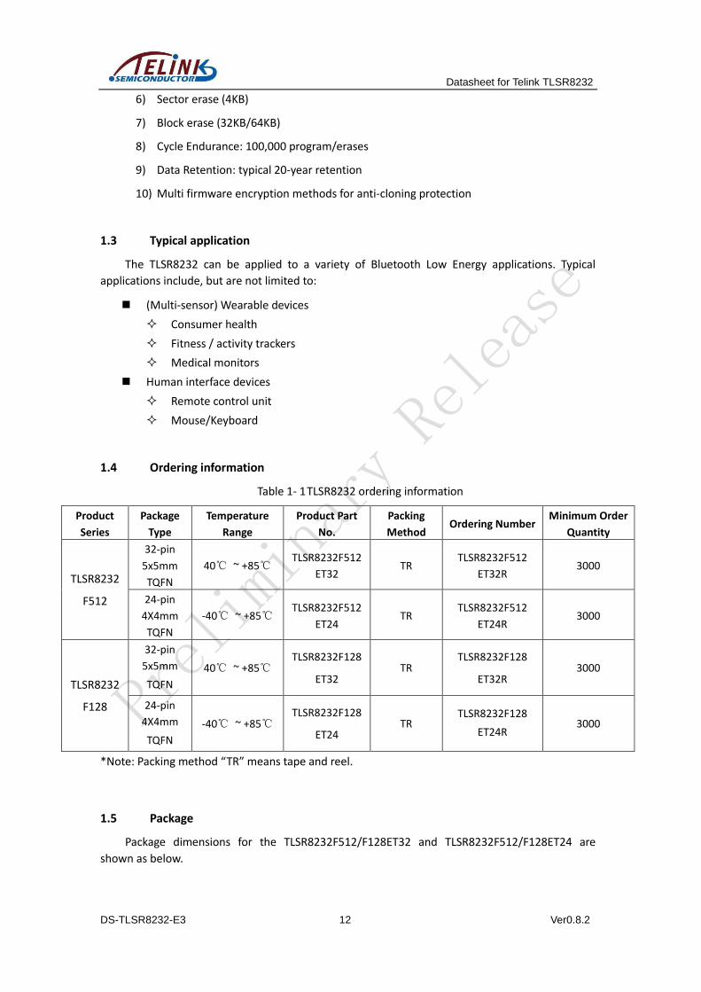
Table 1- 1 TLSR8232 ordering information ......................................................... 12
Table 1- 2 Pin functions for TLSR8232F512/F128ET32 ...................................... 15
Table 1- 3 Pin functions for TLSR8232F512/F128ET24 ...................................... 18
Table 2- 1 Retention analog registers in deep sleep .......................................... 24
Table 2- 2 Register configuration for software reset .......................................... 25
Table 2- 3 Analog register to control delay counter ........................................... 27
Table 2- 4 Characteristics of Power-up/ Power-down sequence ....................... 28
Table 2- 5 Analog registers for module power up/down control ....................... 29
Table 2- 6 Analog registers for Wakeup.............................................................. 31
Table 2- 7 Digital register for Wakeup ................................................................ 32
Table 3- 1 Packet Format in standard 1Mbps BLE mode .................................... 34
Table 3- 2 Packet format in standard 2Mbps BLE mode .................................... 34
Table 3- 3 Packet format in Proprietary mode ................................................... 34
Table 4- 1 Register table related to clock ........................................................... 37
Table 5- 1 Register configuration for Timer0~Timer2 ........................................ 39
Table 5- 2 Register table for System Timer ......................................................... 43
Table 6- 1 Register table for Interrupt system .................................................... 45
Table 7- 1 GPIO lookup table .............................................................................. 48
Table 7- 2 GPIO lookup table2 ............................................................................ 54
Table 7- 3 Analog registers for pull-up/pull-down resistor control .................... 55
Table 7- 4 Register configuration for I2C ............................................................ 59
Table 7- 5 Register configuration for SPI ............................................................ 63
Table 7- 6 SPI mode ............................................................................................ 64
Table 7- 7 Register configuration for UART ........................................................ 66
Table 8- 1 Register table for PWM ..................................................................... 69
Table 9- 1 Input pin selection ............................................................................. 82
Table 9- 2 Timing ................................................................................................ 86
Table 9- 3 Register table for QDEC ..................................................................... 87
Table 10- 1 Overall register setting ...................................................................... 95
Table 10- 2 Register setting for L/R/M channel .................................................... 95
Table 10- 3 Register table related to SAR ADC ..................................................... 97
Table 11- 1 Analog register table related to PGA ............................................... 104
Table 12- 1 Analog register for temperature sensor .......................................... 105
Table 13- 1 Register table related to AES ........................................................... 108
Table 14- 1 Absolute Maximum Ratings ............................................................. 109
Table 14- 2 Recommended operation condition ................................................ 109
Table 14- 3 DC characteristics (T=25℃) ............................................................. 110
Table 14- 4 AC Characteristics ............................................................................ 111
Table 15- 1 BOM table for TLSR8232F512ET32 .................................................. 116
Datasheet for Telink TLSR8232
DS-TLSR8232-E3 9 Ver0.8.2
1 Overview
The TLSR8232 is Telink-developed BLE SoC solution, which is Bluetooth 4.2 fully standard
compliant to allow easy connectivity with Bluetooth Smart Ready mobile phones, tablets, laptops.
The TLSR8232 supports BLE slave and master mode operations. It also supports BLE 5.0 2Mbps
mode and long packet length.
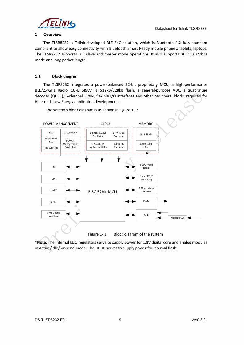
1.1 Block diagram
The TLSR8232 integrates a power-balanced 32-bit proprietary MCU, a high-performance
BLE/2.4GHz Radio, 16kB SRAM, a 512kB/128kB flash, a general-purpose ADC, a quadrature
decoder (QDEC), 6-channel PWM, flexible I/O interfaces and other peripheral blocks required for
Bluetooth Low Energy application development.
The system’s block diagram is as shown in Figure 1-1:
RISC 32bit MCU
Analog PGAADC
Timer0/1/2Watchdog
I2C
SPI
UART
GPIO
24MHz Crystal Oscillator
32.768kHz Crystal Oscillator
24MHz RC Oscillator
32kHz RC Oscillator
CLOCK
RESET
POWER-ON RESET
LDO/DCDC*
POWER Management
ControllerBROWN OUT
BLE/2.4GHz Radio
POWER MANAGEMENT
SWS Debug Interface
1 Quadrature Decoder
16kB SRAM
128/512kB FLASH
MEMORY
PWM
Figure 1- 1 Block diagram of the system
*Note: The internal LDO regulators serve to supply power for 1.8V digital core and analog modules
in Active/Idle/Suspend mode. The DCDC serves to supply power for internal flash.
Datasheet for Telink TLSR8232
DS-TLSR8232-E3 10 Ver0.8.2
1.2 Key features
1.2.1 General features
General features are as follows:
1) 32-bit proprietary microcontroller
Better power-balanced performance than ARM M0
Instruction cache controller with 2kB cache RAM memory
Maximum running speed up to 48MHz
2) Memory architecture
Program memory: 512kB/128kB flash
16kB SRAM
3) Supports BLE and 2.4GHz proprietary protocols
4) RTC and other timers
Clock source of a 24MHz/32kHz Crystal or RC oscillator
Three general 32-bit timers, with four selectable modes in active mode
Watchdog timer
A low-frequency 32kHz timer available in low power mode
5) Digital and analog interfaces
Up to 23 or 16 GPIOs depending on package option
Configurable pull-up or pull-down resistors
SPI and I2C Master/Slave, UART interface
SWS (Single Wire Slave) interface for debugging
One quadrature decoder (QDEC)
Up to 6-channel PWM output
IR transmitter with DMA support
10-channel ADC with 10.5 ENOB
2-channel differential PGA.
6) Hardware AES and random number generator
7) Firmware encryption: support software signature based on flash UID and hardware
encryption based on EFUSE key
8) Operating temperature range: -40℃~+85℃
9) Package:
QFN32 5x5mm, TLSR8232F512/F128ET32
QFN24 4x4mm, TLSR8232F512/F128ET24
Completely RoHS-compliant
Datasheet for Telink TLSR8232
DS-TLSR8232-E3 11 Ver0.8.2
1.2.2 RF Features
RF features include:
1) BLE/2.4GHz RF transceiver in worldwide 2.4GHz ISM band
2) Bluetooth 4.2 Compliant and BLE 5.0 2Mbps and long packet length
3) 2.4GHz proprietary 2Mbps mode with Adaptive Frequency Hopping support
4) Rx Sensitivity: -91dBm @ 1Mbps mode
5) Tx Output power up to +8dBm
6) 50 Ω matched single-pin antenna input
7) RSSI monitoring with +/-4dB resolution
1.2.3 Features of power management module
Features of power management module include:
1) Power supply of 1.9V~3.6V
2) Battery monitor for low battery voltage detection
3) Brownout detection/shutoff and Power-On-Reset
4) Multiple-power-state to optimize power consumption
5) Low power consumption
Transmitter mode current: 14.5mA @ 0dBm power, 25mA @ 8dBm power
Receiver mode current: 16mA
Suspend mode current: 8uA (IO wakeup), 10uA (Timer wakeup)
Deep sleep mode current (Flash not included, without 32kHz external XOSC, and
internal 32kHz RC OSC off): 1uA
Deep sleep mode current (Flash not included, with 32kHz external XOSC, and
internal 32kHz RC OSC off): 1.7uA
Deep sleep mode current (Flash not included, without 32kHz external XOSC, and
internal 32kHz RC OSC on): 2.2uA
1.2.4 Flash features
The TLSR8232 embeds Flash with features below:
1) TLSR8232F512: Total 512KB (4Mbits)
2) TLSR8232F128: Total 128KB (1Mbits)
3) Flexible architecture: 4KB per Sector, 64KB/32KB per block
4) Up to 256 Bytes per programmable page
5) Write protect all or portions of memory
Datasheet for Telink TLSR8232
DS-TLSR8232-E3 12 Ver0.8.2
6) Sector erase (4KB)
7) Block erase (32KB/64KB)
8) Cycle Endurance: 100,000 program/erases
9) Data Retention: typical 20-year retention
10) Multi firmware encryption methods for anti-cloning protection
1.3 Typical application
The TLSR8232 can be applied to a variety of Bluetooth Low Energy applications. Typical
applications include, but are not limited to:
(Multi-sensor) Wearable devices
Consumer health
Fitness / activity trackers
Medical monitors
Human interface devices
Remote control unit
Mouse/Keyboard
1.4 Ordering information
Table 1- 1 TLSR8232 ordering information
Product
Series
Package
Type
Temperature
Range
Product Part
No.
Packing
Method Ordering Number
Minimum Order
Quantity
TLSR8232
F512
32-pin
5x5mm
TQFN
40℃ ~ +85℃ TLSR8232F512
ET32 TR
TLSR8232F512
ET32R 3000
24-pin
4X4mm
TQFN
-40℃ ~ +85℃ TLSR8232F512
ET24 TR
TLSR8232F512
ET24R 3000
TLSR8232
F128
32-pin
5x5mm
TQFN
40℃ ~ +85℃ TLSR8232F128
ET32 TR
TLSR8232F128
ET32R 3000
24-pin
4X4mm
TQFN
-40℃ ~ +85℃ TLSR8232F128
ET24 TR
TLSR8232F128
ET24R 3000
*Note: Packing method “TR” means tape and reel.
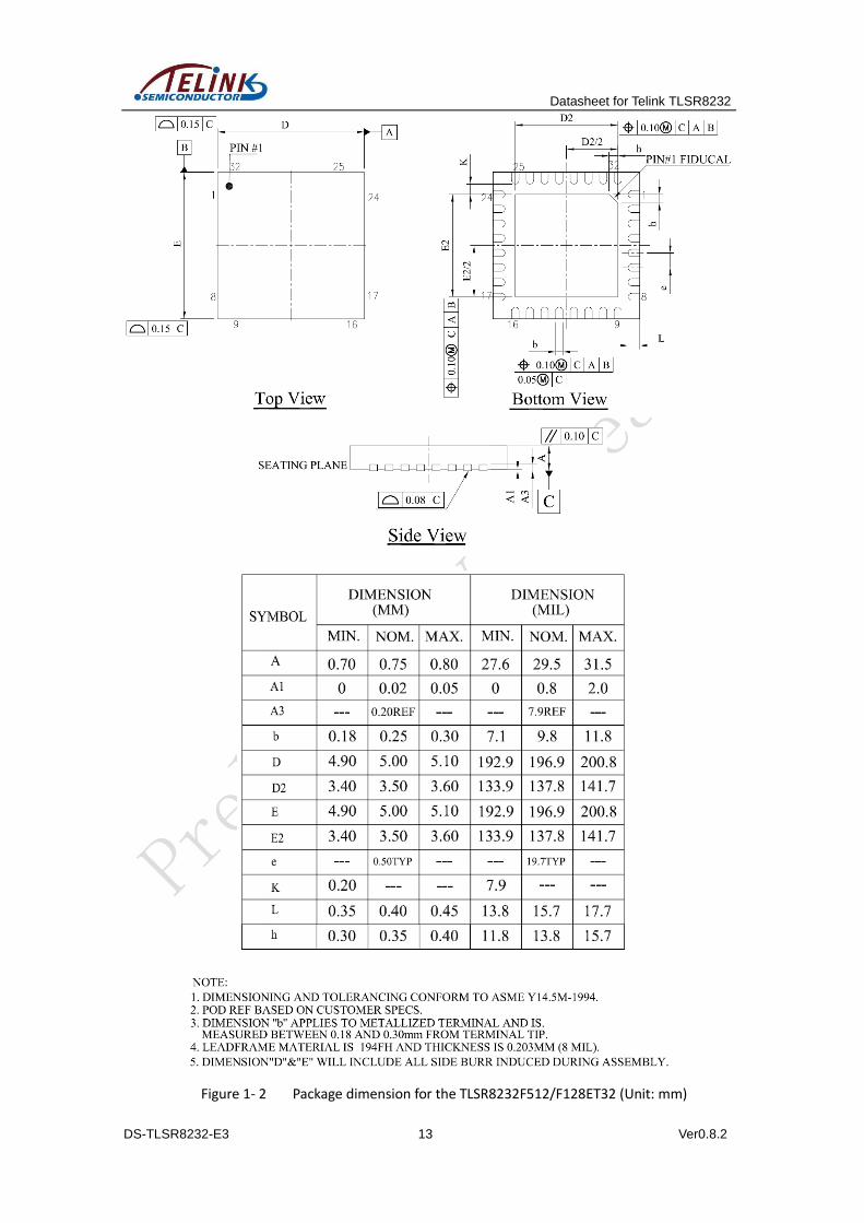
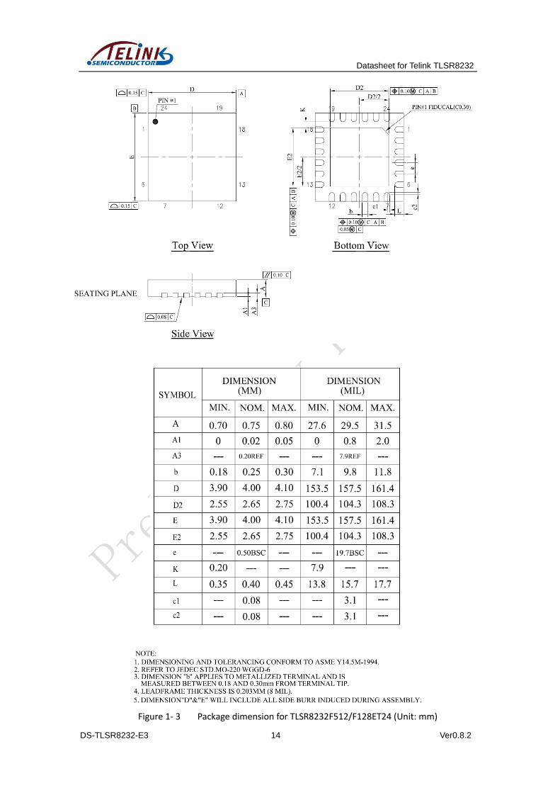
1.5 Package
Package dimensions for the TLSR8232F512/F128ET32 and TLSR8232F512/F128ET24 are
shown as below.
Datasheet for Telink TLSR8232
DS-TLSR8232-E3 13 Ver0.8.2
Figure 1- 2 Package dimension for the TLSR8232F512/F128ET32 (Unit: mm)
Datasheet for Telink TLSR8232
DS-TLSR8232-E3 14 Ver0.8.2
Figure 1- 3 Package dimension for TLSR8232F512/F128ET24 (Unit: mm)
Datasheet for Telink TLSR8232
DS-TLSR8232-E3 15 Ver0.8.2
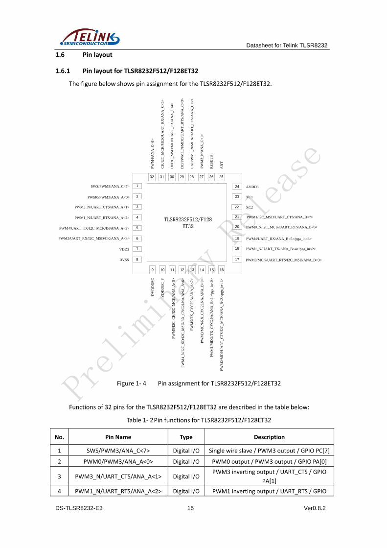
1.6 Pin layout
1.6.1 Pin layout for TLSR8232F512/F128ET32
The figure below shows pin assignment for the TLSR8232F512/F128ET32.
1
2
3
4
5
6
7
8
24
23
22
21
20
19
18
17
9 1110 12 13 14 1615
32 3031 29 28 27 2526
TLSR8232F512/F128ET32
SWS/PWM3/ANA_C<7>
PWM0/PWM3/ANA_A<0>
PWM3_N/UART_CTS/ANA_A<1>
PWM1_N/UART_RTS/ANA_A<2>
VDD3
PWM2/UART_RX/I2C_MSD/CK/ANA_A<4>
DVSS
PWM4/UART_TX/I2C_MCK/DI/ANA_A<3>
DV
DD
DE
C
VD
DD
EC
_F
PW
M5
/I2C
_C
K/I
2C
_M
CK
/AN
A_A
<5>
PW
M4_N
/I2C
_S
D/I
2C
_M
SD
/RX
_C
YC
2L
NA
/AN
A_A
<6>
PW
M5/T
X_C
YC
2P
A/A
NA
_A
<7>
PW
M3/M
CN
/RX
_C
YC
2L
NA
/AN
A_B
<0>
PW
M1/M
DO
/TX
_C
YC
2P
A/A
NA
_B
<1>
/pga_
in<
0>
PW
M2/M
DI/
UA
RT
_C
TS
/I2C
_M
CK
/AN
A_B
<2>
/pga_
in<
1>
PWM0/MCK/UART_RTS/I2C_MSD/ANA_B<3>
PWM4/UART_RX/ANA_B<5>/pga_in<3>
PWM0_N/I2C_MCK/UART_RTS/ANA_B<6>
PWM1/I2C_MSD/UART_CTS/ANA_B<7>
PWM1_N/UART_TX/ANA_B<4>/pga_in<2>
XC1
XC2
AVDD3
AN
T
RE
SE
TB
PW
M2_N
/AN
A_C
<1>
CN
/PW
M0_N
/MC
N/U
AR
T_C
TS
/AN
A_C
<2>
DO
/PW
M5_N
/MD
O/U
AR
T_R
TS
/AN
A_C
<3>
DI/
I2C
_M
SD
/MD
I/U
AR
T_T
X/A
NA
_C
<4>
CK
/I2C
_M
CK
/MC
K/U
AR
T_R
X/A
NA
_C
<5>
PW
M4/A
NA
_C
<6>
Figure 1- 4 Pin assignment for TLSR8232F512/F128ET32
Functions of 32 pins for the TLSR8232F512/F128ET32 are described in the table below:
Table 1- 2 Pin functions for TLSR8232F512/F128ET32
No. Pin Name Type Description
1 SWS/PWM3/ANA_C<7> Digital I/O Single wire slave / PWM3 output / GPIO PC[7]
2 PWM0/PWM3/ANA_A<0> Digital I/O PWM0 output / PWM3 output / GPIO PA[0]
3 PWM3_N/UART_CTS/ANA_A<1> Digital I/O PWM3 inverting output / UART_CTS / GPIO
PA[1]
4 PWM1_N/UART_RTS/ANA_A<2> Digital I/O PWM1 inverting output / UART_RTS / GPIO
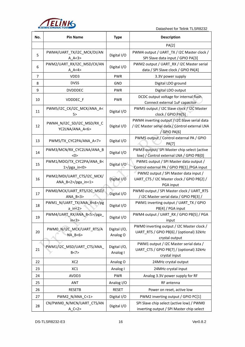
Datasheet for Telink TLSR8232
DS-TLSR8232-E3 16 Ver0.8.2
No. Pin Name Type Description
PA[2]
5 PWM4/UART_TX/I2C_MCK/DI/AN
A_A<3> Digital I/O
PWM4 output / UART_TX / I2C Master clock /
SPI Slave data input / GPIO PA[3]
6 PWM2/UART_RX/I2C_MSD/CK/AN
A_A<4> Digital I/O
PWM2 output / UART_RX / I2C Master serial
data / SPI Slave clock / GPIO PA[4]
7 VDD3 PWR 3.3V power supply
8 DVSS GND Digital LDO ground
9 DVDDDEC PWR Digital LDO output
10 VDDDEC_F PWR DCDC output voltage for internal flash.
Connect external 1uF capacitor
11 PWM5/I2C_CK/I2C_MCK/ANA_A<
5> Digital I/O
PWM5 output / I2C Slave clock / I2C Master
clock / GPIO PA[5]
12 PWM4_N/I2C_SD/I2C_MSD/RX_C
YC2LNA/ANA_A<6> Digital I/O
PWM4 inverting output / I2C Slave serial data
/ I2C Master serial data / Control external LNA
/ GPIO PA[6]
13 PWM5/TX_CYC2PA/ANA_A<7> Digital I/O PWM5 output / Control external PA / GPIO
PA[7]
14 PWM3/MCN/RX_CYC2LNA/ANA_B
<0> Digital I/O
PWM3 output/ SPI Master chip select (active
low) / Control external LNA / GPIO PB[0]
15 PWM1/MDO/TX_CYC2PA/ANA_B<
1>/pga_in<0> Digital I/O
PWM1 output / SPI Master data output /
Control external PA / GPIO PB[1] /PGA input
16 PWM2/MDI/UART_CTS/I2C_MCK/
ANA_B<2>/pga_in<1> Digital I/O
PWM2 output / SPI Master data input /
UART_CTS / I2C Master clock / GPIO PB[2] /
PGA input
17 PWM0/MCK/UART_RTS/I2C_MSD/
ANA_B<3> Digital I/O
PWM0 output / SPI Master clock / UART_RTS
/ I2C Master serial data / GPIO PB[3] /
18 PWM1_N/UART_TX/ANA_B<4>/pg
a_in<2> Digital I/O
PWM1 inverting output / UART_TX / GPIO
PB[4] / PGA input
19 PWM4/UART_RX/ANA_B<5>/pga_
in<3> Digital I/O
PWM4 output / UART_RX / GPIO PB[5] / PGA
input
20 PWM0_N/I2C_MCK/UART_RTS/A
NA_B<6>
Digital I/O,
Analog O
PWM0 inverting output / I2C Master clock /
UART_RTS / GPIO PB[6] / (optional) 32kHz
crystal output
21 PWM1/I2C_MSD/UART_CTS/ANA_
B<7>
Digital I/O,
Analog I
PWM1 output / I2C Master serial data /
UART_CTS / GPIO PB[7] / (optional) 32kHz
crystal input
22 XC2 Analog O 24MHz crystal output
23 XC1 Analog I 24MHz crystal input
24 AVDD3 PWR Analog 3.3V power supply for RF
25 ANT Analog I/O RF antenna
26 RESETB RESET Power on reset, active low
27 PWM2_N/ANA_C<1> Digital I/O PWM2 inverting output / GPIO PC[1]
28 CN/PWM0_N/MCN/UART_CTS/AN
A_C<2> Digital I/O
SPI Slave chip select (active low) / PWM0
inverting output / SPI Master chip select
Datasheet for Telink TLSR8232
DS-TLSR8232-E3 17 Ver0.8.2
No. Pin Name Type Description
(active low) / UART_CTS / GPIO PC[2]
29 DO/PWM5_N/MDO/UART_RTS/A
NA_C<3> Digital I/O
SPI Slave data output / PWM5 inverting
output / SPI Master data output / UART_RTS /
GPIO PC[3]
30 DI/I2C_MSD/MDI/UART_TX/ANA_
C<4> Digital I/O
SPI Slave data input / I2C Master serial data /
SPI Master data input / UART_TX / GPIO PC[4]
31 CK/I2C_MCK/MCK/UART_RX/ANA
_C<5> Digital I/O
SPI Slave clock / I2C Master clock / SPI Master
clock / UART_RX / GPIO PC[5]
32 PWM4/ANA_C<6> Digital I/O PWM4 output / GPIO PC[6]
Datasheet for Telink TLSR8232
DS-TLSR8232-E3 18 Ver0.8.2
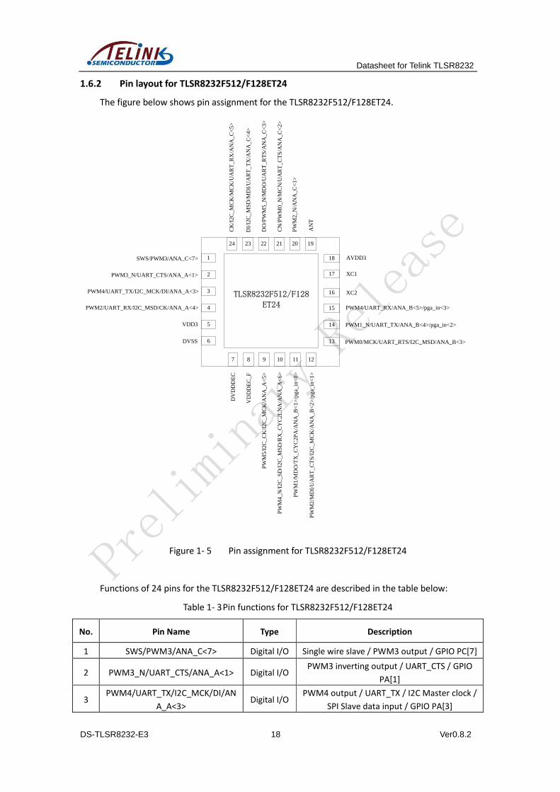
1.6.2 Pin layout for TLSR8232F512/F128ET24
The figure below shows pin assignment for the TLSR8232F512/F128ET24.
1
2
3
4
5
6
18
17
7 98 10 11 12
24 2223 21 20 19
16
15
14
13
TLSR8232F512/F128ET24
SWS/PWM3/ANA_C<7>
PWM3_N/UART_CTS/ANA_A<1>
VDD3
PWM2/UART_RX/I2C_MSD/CK/ANA_A<4>
DVSS
PWM4/UART_TX/I2C_MCK/DI/ANA_A<3>
DV
DD
DE
C
VD
DD
EC
_F
PW
M5
/I2
C_
CK
/I2
C_
MC
K/A
NA
_A
<5
>
PW
M4
_N
/I2
C_
SD
/I2
C_
MS
D/R
X_
CY
C2
LN
A/A
NA
_A
<6
>
PW
M1
/MD
O/T
X_
CY
C2
PA
/AN
A_
B<
1>
/pg
a_in
<0
>
PW
M2
/MD
I/U
AR
T_
CT
S/I
2C
_M
CK
/AN
A_
B<
2>
/pg
a_in
<1
>
PWM0/MCK/UART_RTS/I2C_MSD/ANA_B<3>
PWM1_N/UART_TX/ANA_B<4>/pga_in<2>
PWM4/UART_RX/ANA_B<5>/pga_in<3>
XC1
XC2
AVDD3
AN
T
PW
M2
_N
/AN
A_
C<
1>
CN
/PW
M0
_N
/MC
N/U
AR
T_
CT
S/A
NA
_C
<2
>
DO
/PW
M5
_N
/MD
O/U
AR
T_
RT
S/A
NA
_C
<3
>
DI/
I2C
_M
SD
/MD
I/U
AR
T_
TX
/AN
A_
C<
4>
CK
/I2
C_
MC
K/M
CK
/UA
RT
_R
X/A
NA
_C
<5
>
Figure 1- 5 Pin assignment for TLSR8232F512/F128ET24
Functions of 24 pins for the TLSR8232F512/F128ET24 are described in the table below:
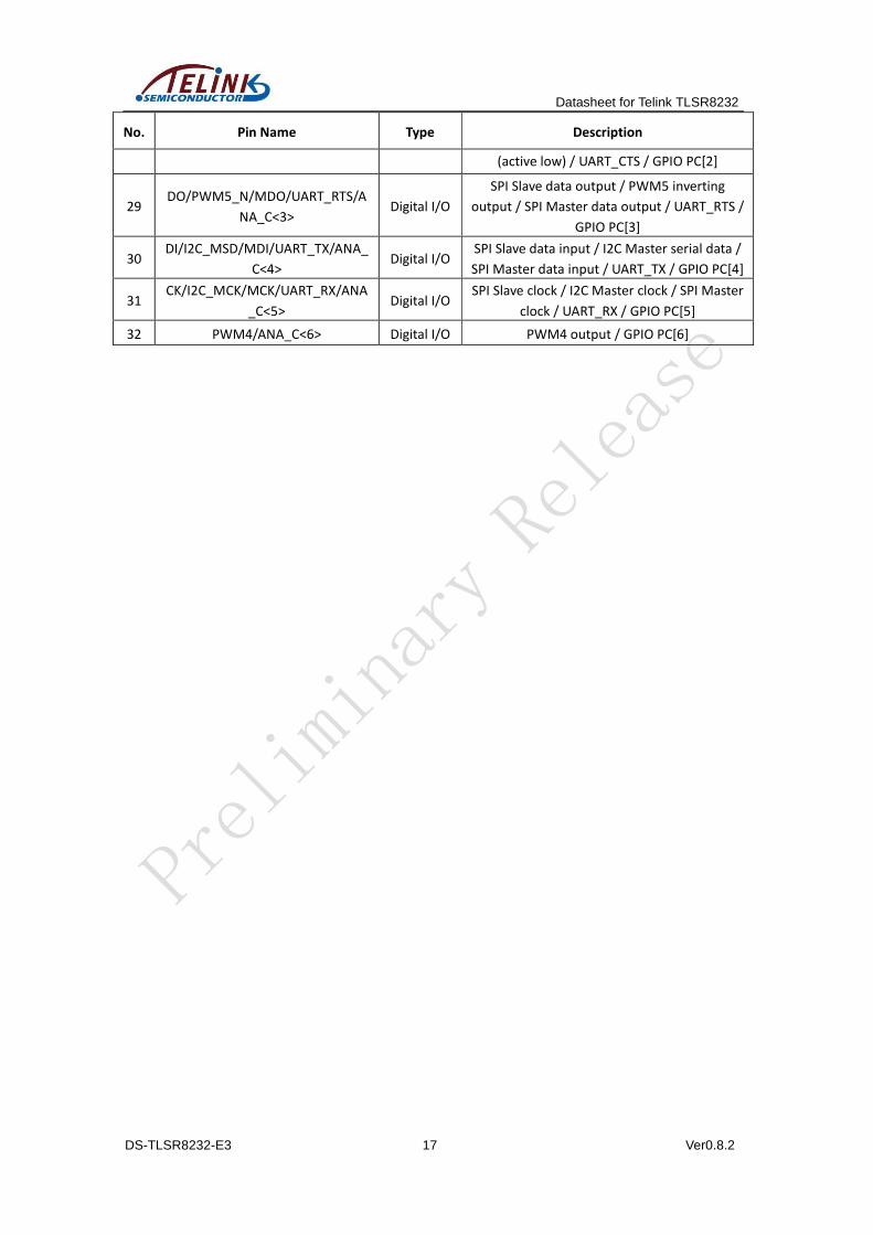
Table 1- 3 Pin functions for TLSR8232F512/F128ET24
No. Pin Name Type Description
1 SWS/PWM3/ANA_C<7> Digital I/O Single wire slave / PWM3 output / GPIO PC[7]
2 PWM3_N/UART_CTS/ANA_A<1> Digital I/O PWM3 inverting output / UART_CTS / GPIO
PA[1]
3 PWM4/UART_TX/I2C_MCK/DI/AN
A_A<3> Digital I/O
PWM4 output / UART_TX / I2C Master clock /
SPI Slave data input / GPIO PA[3]
Datasheet for Telink TLSR8232
DS-TLSR8232-E3 19 Ver0.8.2
No. Pin Name Type Description
4 PWM2/UART_RX/I2C_MSD/CK/AN
A_A<4> Digital I/O
PWM2 output / UART_RX / I2C Master serial
data / SPI Slave clock / GPIO PA[4]
5 VDD3 PWR 3.3V power supply
6 DVSS GND Digital LDO ground
7 DVDDDEC PWR Digital LDO output
8 VDDDEC_F PWR DCDC output voltage for internal flash.
Connect external 1uF capacitor
9 PWM5/I2C_CK/I2C_MCK/ANA_A<
5> Digital I/O
PWM5 output / I2C Slave clock / I2C Master
clock / GPIO PA[5]
10 PWM4_N/I2C_SD/I2C_MSD/RX_C
YC2LNA/ANA_A<6> Digital I/O
PWM4 inverting output / I2C Slave serial data
/ I2C Master serial data / Control external LNA
/ GPIO PA[6]
11 PWM1/MDO/TX_CYC2PA/ANA_B<
1>/pga_in<0> Digital I/O
PWM1 output / SPI Master data output /
Control external PA / GPIO PB[1] /PGA input
12 PWM2/MDI/UART_CTS/I2C_MCK/
ANA_B<2>/pga_in<1> Digital I/O
PWM2 output / SPI Master data input /
UART_CTS / I2C Master clock / GPIO PB[2] /
PGA input
13 PWM0/MCK/UART_RTS/I2C_MSD/
ANA_B<3> Digital I/O
PWM0 output / SPI Master clock / UART_RTS
/ I2C Master serial data / GPIO PB[3] /
14 PWM1_N/UART_TX/ANA_B<4>/pg
a_in<2> Digital I/O
PWM1 inverting output / UART_TX / GPIO
PB[4] / PGA input
15 PWM4/UART_RX/ANA_B<5>/pga_
in<3> Digital I/O
PWM4 output / UART_RX / GPIO PB[5] / PGA
input
16 XC2 Analog O 24MHz crystal output
17 XC1 Analog I 24MHz crystal input
18 AVDD3 PWR Analog 3.3V power supply for RF
19 ANT Analog I/O RF antenna
20 PWM2_N/ANA_C<1> Digital I/O PWM2 inverting output / GPIO PC[1]
21 CN/PWM0_N/MCN/UART_CTS/AN
A_C<2> Digital I/O
SPI Slave chip select (active low) / PWM0
inverting output / SPI Master chip select
(active low) / UART_CTS / GPIO PC[2]
22 DO/PWM5_N/MDO/UART_RTS/A
NA_C<3> Digital I/O
SPI Slave data output / PWM5 inverting
output / SPI Master data output / UART_RTS /
GPIO PC[3]
23 DI/I2C_MSD/MDI/UART_TX/ANA_
C<4> Digital I/O
SPI Slave data input / I2C Master serial data /
SPI Master data input / UART_TX / GPIO PC[4]
24 CK/I2C_MCK/MCK/UART_RX/ANA
_C<5> Digital I/O
SPI Slave clock / I2C Master clock / SPI Master
clock / UART_RX / GPIO PC[5]
Datasheet for Telink TLSR8232
DS-TLSR8232-E3 20 Ver0.8.2
1.6.3 Notes
1) All digital IOs including ANA_A<0> ~ ANA_C<7> can be used as GPIOs and have configurable
pull-up/pull-down resistor.
2) I2C and SPI Master/Slave pins can be configured independently.
Pins marked with I2C_MCK and I2C_MSD can be configured as I2C Master clock and
serial data.
Pins marked with I2C_CK and I2C_SD can be configured as I2C Slave clock and serial
data.
Pins marked with MCN, MDO, MDI and MCK can be configured as SPI Master chip select
(active low), data output, data input and clock.
Pins marked with CN, DO, DI and CK can be configured as SPI Slave chip select (active
low), data output, data input and clock.
ANA_A<3:4>/ANA_C<4:5> SPI Slave DI, CK are multiplexed with I2C Slave I2C_SD, I2C_CK.
Please refer to GPIO lookup table in section 7.1.1.1.
ANA_B<0:3> RX_CYC2LNA, TX_CYC2PA, UART_CTS, UART_RTS are multiplexed with SPI
Slave CN, DO, DI, CK. Please refer to GPIO lookup table in section 7.1.1.1.
3) RX_CYC2LNA & TX_CYC2PA: control enabling external PA/LNA. Please refer to section 3.1 Block diagram.
4) UART with hardware flow control: UART_TX, UART_RX, UART_CTS, UART_RTS.
5) Analog PGA input: ANA_B<1>~ANA_B<2>, ANA_B<4>~ANA_B<5>. Please refer to section 11
PGA.
6) 32kHz crystal input and output: ANA_B<7> and ANA_B<6>.
7) Pin drive strength: ANA_A<0> ~ ANA_C<7> support drive strength up to 8mA (8mA when
“DS”=1, 4mA when “DS”=0). Please refer to section 7.1.1 Basic configuration for the
corresponding “DS” register address and the default setting.
Datasheet for Telink TLSR8232
DS-TLSR8232-E3 21 Ver0.8.2
2 Memory and MCU
2.1 Memory
The TLSR8232 embeds 16kB SRAM, 512kB internal FLASH (TLSR8232F512) or 128kB internal
FLASH (TLSR8232F128).
2.1.1 SRAM/Register
SRAM/Register memory map is shown as follows:
0x808000
0x80BFFF
0x80C000
16kB SRAM
0x807FFF
0x800000
Register
Figure 2- 1 Physical memory map
Register address: 0x800000 ~ 0x807FFF;
16kB SRAM address: 0x808000 ~ 0x80C000.
Both register and 16KB SRAM address can be accessed (read or write) via debugging interface
(SPI/I2C, SWS interface).
2.1.2 Flash
The internal Flash mainly supports page program, sector/block/chip erase operations, and
deep power down operation. Please refer to “AN_RSPH-_Telink RF SoC Programming Handbook”
and “AN_15070101_Telink Internal 512KB (4Mbits) Flash Operation Manual” for Telink Flash
memory details.
For chip identification and traceability, the Flash is preloaded with 20-bit or 28-bit
hexadecimal Unique Chip ID (UID). User is not allowed to modify this preloaded UID, but can read
the UID via corresponding API interface.
Datasheet for Telink TLSR8232
DS-TLSR8232-E3 22 Ver0.8.2
2.2 Firmware encryption
The TLSR8232 supports multiple firmware encryption methods to achieve the anti-cloning
protection, including:
UID-based authentication code generation method
During firmware burning (e.g. via specific burning jig), user can use customized key and AES
encryption algorithm to encrypt the UID read from the chip flash, generate unique
ciphertext and write the ciphertext into specific flash section.
During application, an encryption authentication procedure is added. User should use the
same key and AES encryption algorithm to encrypt the UID read from the chip flash, and
generate new ciphertext. Before running main application firmware, the new ciphertext will
be compared with the ciphertext read from the specific flash section. Only when the
authentication passes, i.e. the comparison result matches, the main firmware will be up and
running, otherwise the chip will stop running the main firmware.
Bootloader-based firmware encryption/decryption
The firmware can be encrypted using a customer-provided security key. The customer
security key is written into E-Fuse, and becomes unreadable. Any attempt to read the key
will only result in either all 1’s or all 0’s.
The encrypted firmware can be generated based on the plaintext firmware and the
customer security key. The customer can burn the security key into the obscured memory
area and also the encrypted firmware into Flash.
The firmware is readable by all, but appears as garbled binaries to 3rd party.
2.3 MCU
The TLSR8232 integrates a powerful 32-bit MCU developed by Telink. The digital core is based
on 32-bit RISC, and the length of instructions is 16 bits; four hardware breakpoints are supported.
Datasheet for Telink TLSR8232
DS-TLSR8232-E3 23 Ver0.8.2
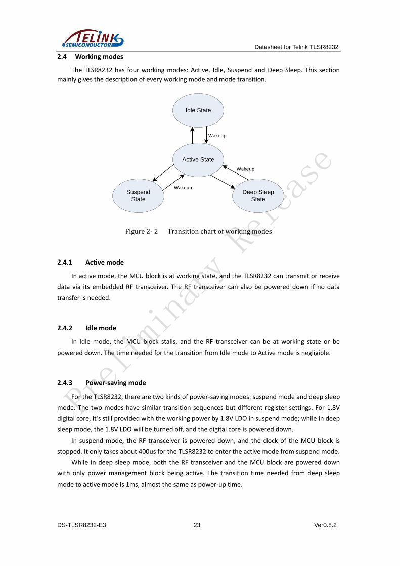
2.4 Working modes
The TLSR8232 has four working modes: Active, Idle, Suspend and Deep Sleep. This section
mainly gives the description of every working mode and mode transition.
Idle State
Suspend
State
Active State
Deep Sleep
State
Wakeup
Wakeup
Wakeup
Figure 2- 2 Transition chart of working modes
2.4.1 Active mode
In active mode, the MCU block is at working state, and the TLSR8232 can transmit or receive
data via its embedded RF transceiver. The RF transceiver can also be powered down if no data
transfer is needed.
2.4.2 Idle mode
In Idle mode, the MCU block stalls, and the RF transceiver can be at working state or be
powered down. The time needed for the transition from Idle mode to Active mode is negligible.
2.4.3 Power-saving mode
For the TLSR8232, there are two kinds of power-saving modes: suspend mode and deep sleep
mode. The two modes have similar transition sequences but different register settings. For 1.8V
digital core, it’s still provided with the working power by 1.8V LDO in suspend mode; while in deep
sleep mode, the 1.8V LDO will be turned off, and the digital core is powered down.
In suspend mode, the RF transceiver is powered down, and the clock of the MCU block is
stopped. It only takes about 400us for the TLSR8232 to enter the active mode from suspend mode.
While in deep sleep mode, both the RF transceiver and the MCU block are powered down
with only power management block being active. The transition time needed from deep sleep
mode to active mode is 1ms, almost the same as power-up time.
Datasheet for Telink TLSR8232
DS-TLSR8232-E3 24 Ver0.8.2
Table 2- 1 Retention analog registers in deep sleep
Address Description Default value
afe_0x34 buffer, watchdog reset/software reset clean 0x00
afe_0x35 buffer, watchdog reset/software reset clean 0x00
afe_0x36 buffer, watchdog reset/software reset clean 0x00
afe_0x37 buffer, watchdog reset/software reset clean 0x00
afe_0x38 buffer, watchdog reset/software reset clean 0x00
afe_0x39 buffer, watchdog reset/software reset clean 0xff
afe_0x3a buffer, only power on reset clean 0x00
afe_0x3b buffer, only power on reset clean 0x00
afe_0x3c buffer, only power on reset clean 0x00
afe_0x3d buffer, only power on reset clean 0x00
afe_0x3e buffer, only power on reset clean 0x00
afe_0x3f buffer, only power on reset clean 0x6f
Analog registers (afe_0x34 ~ afe_0x3f) as shown in Table 2- 1 are retained in deep sleep mode
and can be used to store program state information across deep sleep cycles.
Analog registers afe_0x3a~ afe_0x3f are non-volatile even when chip enters deep sleep or
chip is reset by watchdog or software, i.e. the contents of these registers won’t be changed
by deep sleep or watchdog reset or chip software reset.
Analog registers afe_0x34~ afe_0x39 are non-volatile in deep sleep, but will be cleared by
watchdog reset or chip software reset.
After POR (Power-On-Reset), all registers will be cleared to their default values, including
these analog registers.
User can set flag in these analog registers correspondingly, so as to check the booting source
by reading the flag.
For chip software reset, please refer to section 2.5 Reset.
Datasheet for Telink TLSR8232
DS-TLSR8232-E3 25 Ver0.8.2
2.5 Reset
The chip supports three types of reset methods, including POR (Power-On-Reset), watchdog
reset and software reset.
1) POR: After power on, the whole chip will be reset, and all registers will be cleared to their
default values.
2) Watchdog reset: A programmable watchdog is supported to monitor the system. If watchdog
reset is triggered, registers except for retention analog registers afe_0x3a~ afe_0x3f will be
cleared.
3) Software reset: It is also feasible to carry out software reset for the whole chip or some
modules.
Setting address 0x6f[5] to 1b’1 is to reset the whole chip. Similar to watchdog reset (see
section 2.4.3 Power-saving mode), retention analog registers afe_0x3a~ afe_0x3f are
non-volatile, while other registers including afe_0x34~ afe_0x39 will be cleared by chip
software reset.
Addresses 0x60~0x62 serve to reset individual modules: if some bit is set to logic “1”, the
corresponding module is reset.
Table 2- 2 Register configuration for software reset
Address Mnemonic Type Description Reset Value
0x60 RST0 R/W
Reset control, 1 for reset, 0 for clear
[0]: SPI
[1]: I2C
[2]: n/a
[3]: n/a
[4]: MCU
[5]: n/a
[6]: AIF
[7]: ZB
c0
0x61 RST1 R/W
[0]: system_timer
[1]: algm
[2]: dma
[3]: rs232
[4]: pwm
[5]: aes
[6]: n/a
[7]: swires (SWS)
3f
0x62 RST2 R/W
[0]: n/a
[1]: n/a
[2]: n/a
[3]: adc
[4]: mcic
[5]: soft reset to reset mcic enable
88
Datasheet for Telink TLSR8232
DS-TLSR8232-E3 26 Ver0.8.2
Address Mnemonic Type Description Reset Value
[6]: rsvd (mspi)
[7]: alg
0x6f PWDNEN W
[0]: suspend enable
[5]: rst all (act as watchdog reset)
[6]: rsvd (mcu low power mode)
[7]: stall mcu trig If bit[0] set 1, then
system will go to suspend. Or only
stall mcu.
00
2.6 Power Management
The multiple-stage Power Management (PM) module is flexible to control power state of the
whole chip or individual functional blocks such as MCU, RF Transceiver, and peripherals.
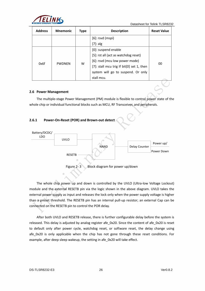
2.6.1 Power-On-Reset (POR) and Brown-out detect
UVLO
NAND Delay Counter
RESETB
Battery/DCDC/LDO
Power up/
Power Down
Figure 2- 3 Block diagram for power up/down
The whole chip power up and down is controlled by the UVLO (Ultra-low Voltage Lockout)
module and the external RESETB pin via the logic shown in the above diagram. UVLO takes the
external power supply as input and releases the lock only when the power supply voltage is higher
than a preset threshold. The RESETB pin has an internal pull-up resistor; an external Cap can be
connected on the RESETB pin to control the POR delay.
After both UVLO and RESETB release, there is further configurable delay before the system is
released. This delay is adjusted by analog register afe_0x20. Since the content of afe_0x20 is reset
to default only after power cycle, watchdog reset, or software reset, the delay change using
afe_0x20 is only applicable when the chip has not gone through these reset conditions. For
example, after deep sleep wakeup, the setting in afe_0x20 will take effect.
Datasheet for Telink TLSR8232
DS-TLSR8232-E3 27 Ver0.8.2
Table 2- 3 Analog register to control delay counter
Address Description Default
afe_0x20
r_dly:
[6:0]: delay, 32kHz decrease counter. Default delay 1ms.
[7] rsvd
0xe0
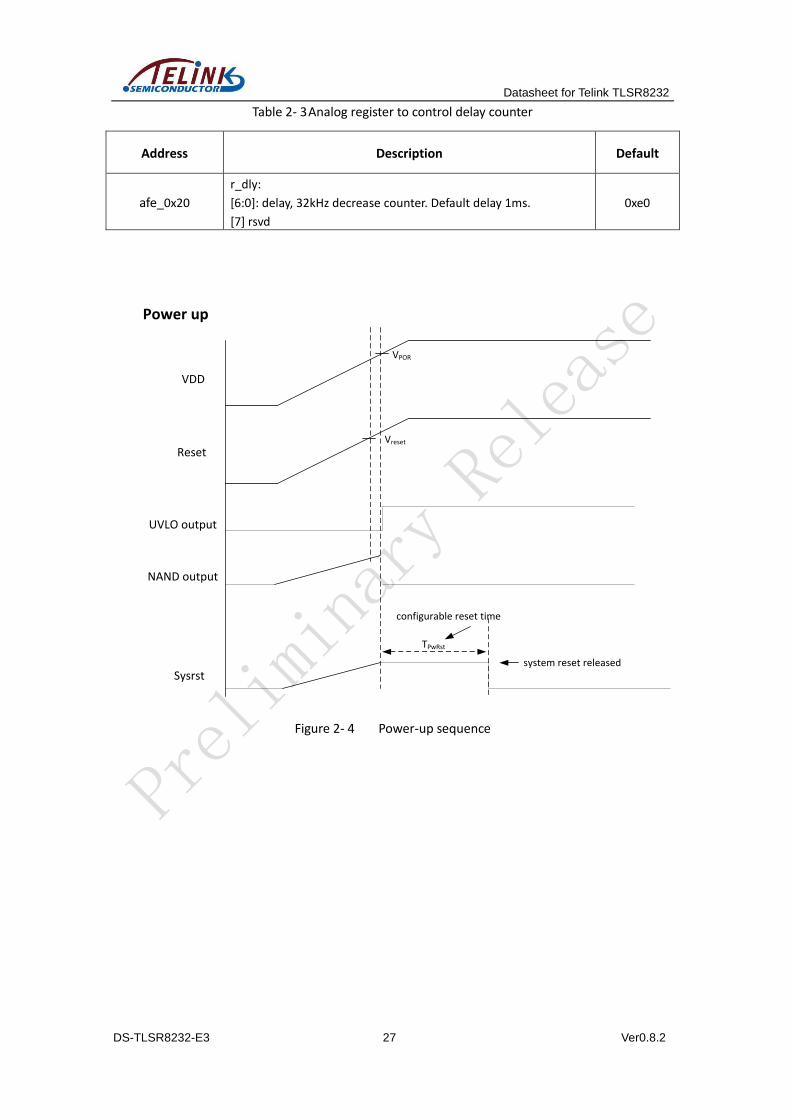
VPOR
VDD
ResetVreset
UVLO output
TPwRst
configurable reset time
system reset releasedSysrst
Power up
NAND output
Figure 2- 4 Power-up sequence
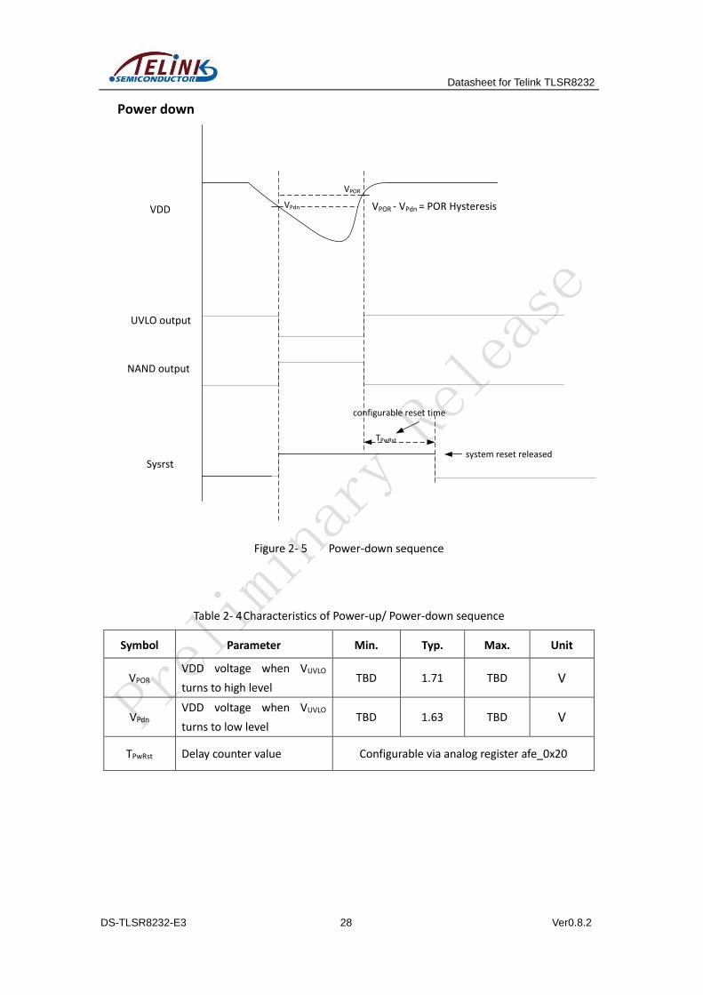
Datasheet for Telink TLSR8232
DS-TLSR8232-E3 28 Ver0.8.2
Power down
VDD VPdn
VPOR
VPOR - VPdn = POR Hysteresis
UVLO output
TPwRst
configurable reset time
system reset releasedSysrst
NAND output
Figure 2- 5 Power-down sequence
Table 2- 4 Characteristics of Power-up/ Power-down sequence
Symbol Parameter Min. Typ. Max. Unit
VPOR VDD voltage when VUVLO
turns to high level TBD 1.71 TBD V
VPdn VDD voltage when VUVLO
turns to low level TBD 1.63 TBD V
TPwRst Delay counter value Configurable via analog register afe_0x20
Datasheet for Telink TLSR8232
DS-TLSR8232-E3 29 Ver0.8.2
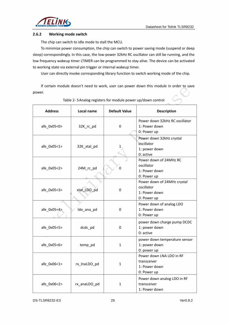
2.6.2 Working mode switch
The chip can switch to idle mode to stall the MCU.
To minimize power consumption, the chip can switch to power saving mode (suspend or deep
sleep) correspondingly. In this case, the low-power 32kHz RC oscillator can still be running, and the
low frequency wakeup timer LTIMER can be programmed to stay alive. The device can be activated
to working state via external pin trigger or internal wakeup timer.
User can directly invoke corresponding library function to switch working mode of the chip.
If certain module doesn’t need to work, user can power down this module in order to save
power.
Table 2- 5 Analog registers for module power up/down control
Address Local name Default Value Description
afe_0x05<0> 32K_rc_pd 0
Power down 32kHz RC oscillator
1: Power down
0: Power up
afe_0x05<1> 32K_xtal_pd 1
Power down 32kHz crystal
oscillator
1: power down
0: active
afe_0x05<2> 24M_rc_pd 0
Power down of 24MHz RC
oscillator
1: Power down
0: Power up
afe_0x05<3> xtal_LDO_pd 0
Power down of 24MHz crystal
oscillator
1: Power down
0: Power up
afe_0x05<4> ldo_ana_pd 0
Power down of analog LDO
1: Power down
0: Power up
afe_0x05<5> dcdc_pd 0
power down charge pump DCDC
1: power down
0: active
afe_0x05<6> temp_pd 1
power down temperature sensor
1: power down
0: power up
afe_0x06<1> rx_lnaLDO_pd 1
Power down LNA LDO in RF
transceiver
1: Power down
0: Power up
afe_0x06<2> rx_anaLDO_pd 1
Power down analog LDO in RF
transceiver
1: Power down
Datasheet for Telink TLSR8232
DS-TLSR8232-E3 30 Ver0.8.2
Address Local name Default Value Description
0: Power up
afe_0x06<3> rx_rfLDO_pd 1
Power down RF LDO in RF
transceiver
1: Power down
0: Power up
afe_0x06<4> pll_BG_pd 1
Power down Bandgap in PLL
1: Power down
0: Power up
afe_0x06<6> pll_vco_ldo_pd 1
Power down VCO LDO
1: Power down
0: Power up
afe_0x06<7> pll_cp_ldo_pd 1
Power down cp and prescaler
analog circuit ldo
1: Power down
0: power up
2.6.3 LDO and DCDC
The chip embeds LDO regulators to generate 1.8V regulated voltage. The internal LDO
regulators serve to supply power for 1.8V digital core and analog modules in Active/Idle/Suspend
mode.
The chip also embeds a boost DCDC which can step up input voltage to the range of 2.7~3.6V.
The DCDC output voltage supplies power for internal flash via the VDDDEC_F pin of the chip.
While in deep sleep mode, the embedded 1.8V LDO regulators and the boost DCDC will be
turned off.
2.7 Wakeup sources
Wakeup_timer
wakeup
IO wakeup
PM_TOP
32K timer
Figure 2- 6 Wakeup sources
Datasheet for Telink TLSR8232
DS-TLSR8232-E3 31 Ver0.8.2
2.7.1 Wakeup source – 32K timer
This wakeup source is able to wake up the system from suspend mode or deep sleep mode.
Address afe_0x26 bit[6] is the enabling bit for wakeup source from 32k timer.
2.7.2 Wakeup source – IO
This wakeup source is able to wake up the system from suspend mode or deep sleep mode.
And IO wakeup supports high level or low level wakeup which is configurable via wakeup polarity
control registers. Total wakeup pin can be up to 23.
Address afe_0x26[4] should be set as 1b’1 to enable IO wakeup source.
Enabling control registers: PA[7:0] enabling control register is afe_0x27[7:0], PB[7:0] enabling
control register is afe_0x28[7:0], PC[7:1] enabling control register is afe_0x29[7:1].
Polarity control registers: PA[7:0] polarity control register is afe_0x21[7:0], PB[7:0] polarity
control register is afe_0x22[7:0], PC[7:1] polarity control register is afe_0x23[7:1].
The corresponding driver is available so that user can directly invoke it to use IO wakeup
source.
2.7.3 Register table
Table 2- 6 Analog registers for Wakeup
Address Description Default Value
afe_0x21 pa_polarity: PA wakeup polarity select
0: high level, 1: low level 0x00
afe_0x22 pb_polarity: PB wakeup polarity select
0: high level, 1: low level 0x00
afe_0x23 pc_polarity: PC wakeup polarity select
0: high level, 1: low level 0x00
afe_0x26[3]
Enable/Mask filter for IO (Pad) wakeup
1: Select 16us filter to filter out jitter on IO PAD
input.
0: IO Pad combinational logic output (disable filter) 0x00
afe_0x26[4] 1: Enable IO (pad) wakeup
afe_0x26[5] Rsvd (Enable dig wakeup)
afe_0x26[6] 1: Enable 32kHz timer wakeup
afe_0x27 wkup_pa_en:
1: Enable PA IO (pad) wakeup 0x00
afe_0x28 wkup_pb_en:
1: Enable PB IO (pad) wakeup 0x00
afe_0x29 wkup_pc_en: 0x00
Datasheet for Telink TLSR8232
DS-TLSR8232-E3 32 Ver0.8.2
Address Description Default Value
1: Enable PC IO (pad) wakeup
afe_0x44
State flag bits
[1]: pm_irq, i.e. 32kHz timer wakeup status
[2]: rsvd (dig wakeup status)
[3] wkup_pad, i.e. IO wakeup status.
Write 1 to clean.
e.g. If bit[3] is 1, it indicates the system is wakened up
by IO (pad) source.
0x00
Table 2- 7 Digital register for Wakeup
Address Mnemonic Type Description Reset Value
0x6e WAKEUPEN R/W
Wakeup enable
[0]: rsvd (enable wakeup from I2C
host)
[1]: rsvd (enable wakeup from SPI
host)
[2]: rsvd
[3]: enable wakeup from gpio
[4]: rsvd (enable wakeup from QDEC
synchronous interface)
System resume control
[7]: sleep wakeup reset system
enable
00
Datasheet for Telink TLSR8232
DS-TLSR8232-E3 33 Ver0.8.2
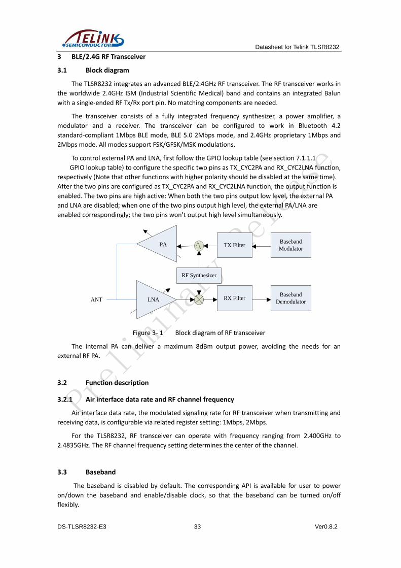
3 BLE/2.4G RF Transceiver
3.1 Block diagram
The TLSR8232 integrates an advanced BLE/2.4GHz RF transceiver. The RF transceiver works in
the worldwide 2.4GHz ISM (Industrial Scientific Medical) band and contains an integrated Balun
with a single-ended RF Tx/Rx port pin. No matching components are needed.
The transceiver consists of a fully integrated frequency synthesizer, a power amplifier, a
modulator and a receiver. The transceiver can be configured to work in Bluetooth 4.2
standard-compliant 1Mbps BLE mode, BLE 5.0 2Mbps mode, and 2.4GHz proprietary 1Mbps and
2Mbps mode. All modes support FSK/GFSK/MSK modulations.
To control external PA and LNA, first follow the GPIO lookup table (see section 7.1.1.1
GPIO lookup table) to configure the specific two pins as TX_CYC2PA and RX_CYC2LNA function,
respectively (Note that other functions with higher polarity should be disabled at the same time).
After the two pins are configured as TX_CYC2PA and RX_CYC2LNA function, the output function is
enabled. The two pins are high active: When both the two pins output low level, the external PA
and LNA are disabled; when one of the two pins output high level, the external PA/LNA are
enabled correspondingly; the two pins won’t output high level simultaneously.
LNA
TX Filter
RX Filter
Baseband
Modulator
Baseband
Demodulator
RF Synthesizer
ANT
PA
Figure 3- 1 Block diagram of RF transceiver
The internal PA can deliver a maximum 8dBm output power, avoiding the needs for an
external RF PA.
3.2 Function description
3.2.1 Air interface data rate and RF channel frequency
Air interface data rate, the modulated signaling rate for RF transceiver when transmitting and
receiving data, is configurable via related register setting: 1Mbps, 2Mbps.
For the TLSR8232, RF transceiver can operate with frequency ranging from 2.400GHz to
2.4835GHz. The RF channel frequency setting determines the center of the channel.
3.3 Baseband
The baseband is disabled by default. The corresponding API is available for user to power
on/down the baseband and enable/disable clock, so that the baseband can be turned on/off
flexibly.
Datasheet for Telink TLSR8232
DS-TLSR8232-E3 34 Ver0.8.2
The baseband contains dedicated hardware logic to perform fast AGC control, access code
correlation, CRC checking, data whitening, encryption/decryption and frequency hopping logic.
The baseband supports all features required by Bluetooth V4.2 specification. It also supports
BLE 5.0 2Mbps mode and long packet length.
3.3.1 Packet format
Packet format in standard 1Mbps BLE mode is shown as Table 3- 1:
Table 3- 1 Packet Format in standard 1Mbps BLE mode
LSB MSB
Preamble
(1 octet)
Access Address
(4 octets)
PDU
(2 ~ 257 octets)
CRC
(3 octets)
Packet length 80bit ~ 2120bit (80~2120us @ 1Mbps).
Packet format in standard 2Mbps BLE mode is shown as Table 3- 2:
Table 3- 2 Packet format in standard 2Mbps BLE mode
LSB MSB
Preamble
(2 octets)
Access Address
(4 octets)
PDU
(2 ~ 257 octets)
CRC
(3 octets)
Packet format in 2.4GHz Proprietary mode is shown as Table 3- 3:
Table 3- 3 Packet format in Proprietary mode
LSB MSB
Preamble
(8 bits)
Address code
(configurable 3~5 bytes)
Packet Controller + Payload
(1~63 bytes)
CRC
(1~2 bytes)
3.3.2 RSSI and frequency offset
The TLSR8232 provides accurate RSSI (Receiver Signal Strength Indicator) and frequency
offset indication.
RSSI can be read from the 1byte at the tail of each received data packet.
If no data packet is received (e.g. carrier or interfering Wi-Fi signal is detected), real-time RSSI
can also be read from specific registers which will be updated automatically.
RSSI resolution can reach +/-4dB.
Frequency offset can be read from the 2bytes at the tail of the data packet. Valid bits of
actual frequency offset may be less than 16bits, and different valid bits correspond to
different tolerance range.
Telink supplies corresponding drivers for user to read RSSI and frequency offset as needed.
Datasheet for Telink TLSR8232
DS-TLSR8232-E3 35 Ver0.8.2
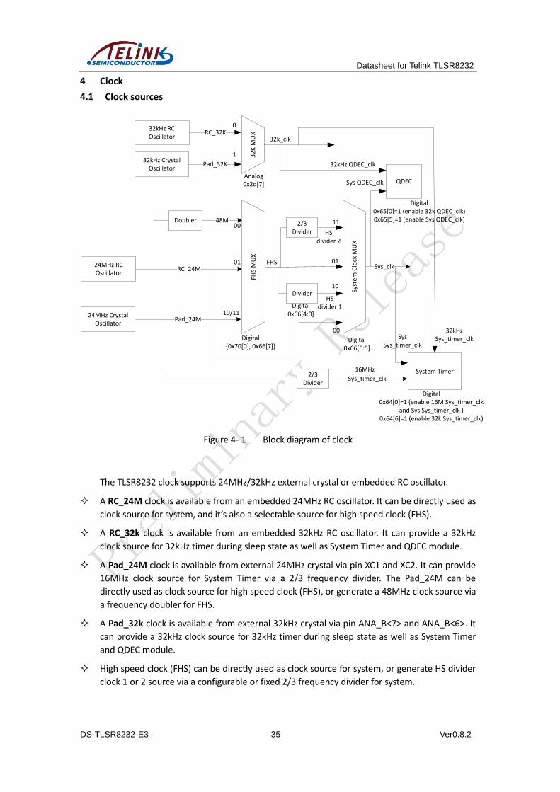
4 Clock
4.1 Clock sources
48M
RC_24M24MHz RC Oscillator
Pad_24M24MHz Crystal
Oscillator
FHS
MU
X
00
01
10/11
Doubler
Digital{0x70[0], 0x66[7]}
Syst
em
Clo
ck M
UX
Divider
FHS
Digital0x66[4:0]
01
10
11
00
Digital 0x66[6:5]
Sys_clk
2/3Divider
Sys_timer_clk
16MHz
32
K M
UX
32k_clkRC_32K
Analog0x2d[7]
32kHz RC Oscillator
0
32kHz Crystal Oscillator
Pad_32K
1
HS divider 1
2/3Divider HS
divider 2
32kHz QDEC_clk
System Timer
QDEC
32kHz Sys_timer_clk
Digital 0x64[0]=1 (enable 16M Sys_timer_clk
and Sys Sys_timer_clk )0x64[6]=1 (enable 32k Sys_timer_clk)
Digital 0x65[0]=1 (enable 32k QDEC_clk)0x65[5]=1 (enable Sys QDEC_clk)
Sys Sys_timer_clk
Sys QDEC_clk
Figure 4- 1 Block diagram of clock
The TLSR8232 clock supports 24MHz/32kHz external crystal or embedded RC oscillator.
A RC_24M clock is available from an embedded 24MHz RC oscillator. It can be directly used as
clock source for system, and it’s also a selectable source for high speed clock (FHS).
A RC_32k clock is available from an embedded 32kHz RC oscillator. It can provide a 32kHz
clock source for 32kHz timer during sleep state as well as System Timer and QDEC module.
A Pad_24M clock is available from external 24MHz crystal via pin XC1 and XC2. It can provide
16MHz clock source for System Timer via a 2/3 frequency divider. The Pad_24M can be
directly used as clock source for high speed clock (FHS), or generate a 48MHz clock source via
a frequency doubler for FHS.
A Pad_32k clock is available from external 32kHz crystal via pin ANA_B<7> and ANA_B<6>. It
can provide a 32kHz clock source for 32kHz timer during sleep state as well as System Timer
and QDEC module.
High speed clock (FHS) can be directly used as clock source for system, or generate HS divider
clock 1 or 2 source via a configurable or fixed 2/3 frequency divider for system.
Datasheet for Telink TLSR8232
DS-TLSR8232-E3 36 Ver0.8.2
4.2 System clock
There are four selectable clock sources for MCU system clock: RC_24M (derived from 24MHz
RC oscillator), High speed clock “FHS”, HS divider clock 1 (derived from “FHS” via a configurable
frequency divider), HS divider clock 2 (derived from “FHS” via a fixed 2/3 frequency divider).
The high speed clock (FHS) is selectable via address {0x70[0], 0x66[7]} from the following
sources: 48MHz clock (derived from 24MHz crystal oscillator via a frequency doubler), RC_24M
(derived from 24MHz RC oscillator), and Pad_24M (derived from 24MHz crystal oscillator).
The digital register CLKSEL (address 0x66) serves to set system clock: System clock source is
selectable via bit[6:5].
If address 0x66[6:5] is set to 2b’00 to select the RC_24M, system clock frequency equals
24MHz.
If address 0x66[6:5] is set to 2b’01 to select the FHS clock, system clock frequency equals the
FHS frequency (FFHS).
If address 0x66[6:5] is set to 2b’10 to select the HS divider clock 1, system clock frequency is
adjustable via address 0x66[4:0]. The formula is shown as below:
FSystem clock = FFHS / (system clock divider value in address 0x66[4:0]).
If address 0x66[6:5] is set to 2b’11 to select the HS divider clock 2, system clock frequency
equals FFHS * 2/3.
4.3 Module clock
Registers CLKEN0~CLKEN2 (address 0x63~0x65) are used to enable or disable clock for various
modules. By disable the clocks of unused modules, current consumption could be reduced.
4.3.1 System Timer clock
System Timer simultaneously uses system clock, a 16MHz clock, as well as a 32kHz clock.
The 16MHz clock is derived from 24MHz crystal oscillator via a 2/3 frequency divider.
The 32kHz clock is selectable as Pad_32k or RC_32k via analog register afe_0x2d[7].
Digital register 0x64 bit[0] and bit[6] should be enabled to drive the System Timer by the
16MHz clock, system clock, as well as the 32kHz clock.
4.3.2 QDEC clock
QDEC module simultaneously uses system clock as well as a 32kHz clock.
The 32kHz clock is selectable as Pad_32k or RC_32k via analog register afe_0x2d[7].
Digital register 0x65 bit[0] and bit[5] should be enabled to drive the whole QDEC module by
the 32kHz clock and system clock.
Datasheet for Telink TLSR8232
DS-TLSR8232-E3 37 Ver0.8.2
4.4 Register table
Table 4- 1 Register table related to clock
Address Mnemonic R/W Description Default
Digital register
0x63 CLKEN0 R/W
Clock enable control: 1 for enable; 0 for disable
[0]: SPI
[1]: I2C
[2]: HOSTIRQ
[3]: n/a
[4]: MCU
[5]: FPU (Float Point Unit)
[6]: AIF
[7]: ZB
13
0x64 CLKEN1 R/W
Clock enable control: 1 for enable; 0 for disable
[0]: System timer (16M_clk and sys_clk for System timer)
[1]: ALGM
[2]: DMA
[3]: RS232
[4]: PWM
[5]: AES
[6]: 32k_clk for system timer
[7]: SWS
80
0x65 CLKEN2 R/W
Clock enable control: 1 for enable; 0 for disable
[0]: 32k_clk for QDEC
[1:3]: n/a
[4]: MCIC
[5]: QDEC (sys_clk for QDEC)
[6:7]: n/a
10
0x66 CLKSEL R/W
System clock select
[4:0]: system clock divider.
If 0x66[6:5] is set as 2b’ 10, FSysclk = FFHS / CLKSEL[4:0].
FHS: refer to 0x70 FHS_sel.
[6:5]: select system clock source
2’b00: RC_24M from RC oscillator
2’b01: FHS clock (High speed clock)
2’b10: HS divider clock 1 derived from FHS clock via a
configurable divider (see 0x66[4:0])
2’b11: HS divider clock 2 derived from FHS clock via a fixed
2/3 divider
{0x70[0], 0x66[7]}: FHS select
06
0x70 FHS_sel R/W
{0x70[0], 0x66[7]}: FHS select
2’b00: 48MHz clock doubled from 24MHz crystal oscillator
2’b01: RC_24M from RC oscillator
2’b1x: Pad_24M from 24MHz crystal oscillator
00
Datasheet for Telink TLSR8232
DS-TLSR8232-E3 38 Ver0.8.2
Address Mnemonic R/W Description Default
Analog register
afe_0x2d R/W
[7] select source for 32kHz clock
0: RC_32k from 32kHz RC oscillator
1: Pad_32k from 32kHz crystal oscillator
0
Datasheet for Telink TLSR8232
DS-TLSR8232-E3 39 Ver0.8.2
5 Timers
5.1 Timer0~Timer2
The TLSR8232 supports three general 32-bit timers in active mode, including Timer0~ Timer2.
All of the three timers support four modes: Mode 0 (System Clock Mode), Mode 1 (GPIO Trigger
Mode), Mode 2 (GPIO Pulse Width Mode) and Mode 3 (Tick Mode), which are selectable via the
register TMR_CTRL0 (address 0x620) ~ TMR_CTRL1 (address 0x621).
Timer 2 can also be configured as “watchdog” timer to monitor firmware running.
5.1.1 Register table
Table 5- 1 Register configuration for Timer0~Timer2
Address Mnemonic Type Description Reset
Value
0x72 Wd_status R/W [0] watch dog status, write 1 to clear.
0x620 TMR_CTRL0 RW
[0]Timer0 enable
1: enable
[2:1] Timer0 mode.
0: using sclk, 1: using gpio,
2: count width of gpi, 3: tick
[3]Timer1 enable
[5:4] Timer1 mode.
[6]Timer2 enable
[7]Bit of timer2 mode
00
0x621 TMR_CTRL1 RW [0]Bit of timer2 mode
[7:1]Low bits of watch dog capture 00
0x622 TMR_CTRL2 RW
[6:0]High bits of watch dog capture.
Watch dog capture is compared with
[31:18] of timer2 ticker.
[7]watch dog capture enable
1: enable
00
0x623 TMR_STATUS RW
[0] timer0 status, write 1 to clear
[1] timer1 status, write 1 to clear
[2] timer2 status, write 1 to clear
0x624 TMR_CAPT0_0 RW Byte 0 of timer0 capture 00
0x625 TMR_CAPT0_1 RW Byte 1 of timer0 capture 00
0x626 TMR_CAPT0_2 RW Byte 2 of timer0 capture 00
0x627 TMR_CAPT0_3 RW Byte 3 of timer0 capture 00
0x628 TMR_CAPT1_0 RW Byte 0 of timer1 capture 00
0x629 TMR_CAPT1_1 RW Byte 1 of timer1 capture 00
0x62a TMR_CAPT1_2 RW Byte 2 of timer1 capture 00
0x62b TMR_CAPT1_3 RW Byte 3 of timer1 capture 00
0x62c TMR_CAPT2_0 RW Byte 0 of timer2 capture 00
0x62d TMR_CAPT2_1 RW Byte 1 of timer2 capture 00
0x62e TMR_CAPT2_2 RW Byte 2 of timer2 capture 00
0x62f TMR_CAPT2_3 RW Byte 3 of timer2 capture 00
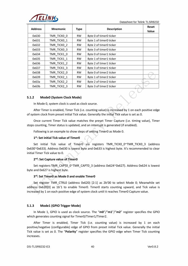
Datasheet for Telink TLSR8232
DS-TLSR8232-E3 40 Ver0.8.2
Address Mnemonic Type Description Reset
Value
0x630 TMR_TICK0_0 RW Byte 0 of timer0 ticker
0x631 TMR_TICK0_1 RW Byte 1 of timer0 ticker
0x632 TMR_TICK0_2 RW Byte 2 of timer0 ticker
0x633 TMR_TICK0_3 RW Byte 3 of timer0 ticker
0x634 TMR_TICK1_0 RW Byte 0 of timer1 ticker
0x635 TMR_TICK1_1 RW Byte 1 of timer1 ticker
0x636 TMR_TICK1_2 RW Byte 2 of timer1 ticker
0x637 TMR_TICK1_3 RW Byte 3 of timer1 ticker
0x638 TMR_TICK2_0 RW Byte 0 of timer2 ticker
0x639 TMR_TICK2_1 RW Byte 1 of timer2 ticker
0x63a TMR_TICK2_2 RW Byte 2 of timer2 ticker
0x63b TMR_TICK2_3 RW Byte 3 of timer2 ticker
5.1.2 Mode0 (System Clock Mode)
In Mode 0, system clock is used as clock source.
After Timer is enabled, Timer Tick (i.e. counting value) is increased by 1 on each positive edge
of system clock from preset initial Tick value. Generally the initial Tick value is set as 0.
Once current Timer Tick value matches the preset Timer Capture (i.e. timing value), Timer
stops counting, Timer status is updated, and an interrupt is generated (if enabled).
Following is an example to show steps of setting Timer0 as Mode 0.
1st: Set initial Tick value of Timer0
Set initial Tick value of Timer0 via registers TMR_TICK0_0~TMR_TICK0_3 (address
0x630~0x633). Address 0x630 is lowest byte and 0x633 is highest byte. It’s recommended to clear
initial Timer Tick value to 0.
2nd: Set Capture value of Timer0
Set registers TMR_CAPT0_0~TMR_CAPT0_3 (address 0x624~0x627). Address 0x624 is lowest
byte and 0x627 is highest byte.
3rd: Set Timer0 as Mode 0 and enable Timer0
Set register TMR_CTRL0 (address 0x620) [2:1] as 2b’00 to select Mode 0; Meanwhile set
address 0x620[0] as 1b’1 to enable Timer0. Timer0 starts counting upward, and Tick value is
increased by 1 on each positive edge of system clock until it reaches Timer0 Capture value.
5.1.3 Mode1 (GPIO Trigger Mode)
In Mode 1, GPIO is used as clock source. The “m0”/“m1”/“m2” register specifies the GPIO
which generates counting signal for Timer0/Timer1/Timer2.
After Timer is enabled, Timer Tick (i.e. counting value) is increased by 1 on each
positive/negative (configurable) edge of GPIO from preset initial Tick value. Generally the initial
Tick value is set as 0. The “Polarity” register specifies the GPIO edge when Timer Tick counting
increases.
Datasheet for Telink TLSR8232
DS-TLSR8232-E3 41 Ver0.8.2
Note: Refer to Section 7.1.2 for corresponding “m0”, “m1”, “m2” and “Polarity” register address.
Once current Timer Tick value matches the preset Timer Capture (i.e. timing value), timer
stops counting and an interrupt is generated (if enabled).
Following is an example to show steps of setting Timer1 as Mode 1.
1st: Set initial Tick value of Timer1
Set initial Tick value of Timer1 via registers TMR_TICK1_0~TMR_TICK1_3 (address
0x634~0x637). Address 0x634 is lowest byte and 0x637 is highest byte. It’s recommended to clear
initial Timer Tick value to 0.
2nd: Set Capture value of Timer1
Set registers TMR_CAPT1_0~TMR_CAPT1_3 (address 0x628~0x62b). Address 0x628 is lowest
byte and 0x62b is highest byte.
3rd: Select GPIO source and edge for Timer1
Select certain GPIO to be the clock source via setting “m1” register.
Select positive edge or negative edge of GPIO input to trigger Timer1 Tick increment via
setting “Polarity” register.
4th: Set Timer1 as Mode 1 and enable Timer1
Set address 0x620[5:4] as 2b’01 to select Mode 1; Meanwhile set address 0x620[3] as 1b’1 to
enable Timer1. Timer1 starts counting upward, and Timer1 Tick value is increased by 1 on each
positive/negative (specified during the 3rd step) edge of the specified GPIO input until it reaches
Timer1 Capture value.
5.1.4 Mode2 (GPIO Pulse Width Mode)
In Mode 2, system clock is used as the unit to measure the width of GPIO pulse. The
“m0”/“m1”/“m2” register specifies the GPIO which generates control signal for
Timer0/Timer1/Timer2.
After Timer is enabled, Timer Tick is triggered by a positive/negative (configurable) edge of
GPIO pulse. Then Timer Tick (i.e. counting value) is increased by 1 on each positive edge of system
clock from preset initial Tick value. Generally the initial Tick value is set as 0. The “Polarity”
register specifies the GPIO edge when Timer Tick starts counting.
Note: Refer to Section 7.1.2 for corresponding “m0”, “m1”, “m2” and “Polarity” register address.
While a negative/positive edge of GPIO pulse is detected, timer stops counting and an
interrupt is generated (if enabled). The GPIO pulse width could be calculated in terms of tick count
and period of system clock.
Following is an example to show steps of setting Timer2 as Mode 2.
1st: Set initial Timer2 Tick value
Set Initial value of Tick via registers TMR_TICK2_0~TMR_TICK2_3 (address 0x638~0x63b).
Address 0x638 is lowest byte and 0x63b is highest byte. It’s recommended to clear initial Timer
Tick value to 0.
2nd: Select GPIO source and edge for Timer2
Datasheet for Telink TLSR8232
DS-TLSR8232-E3 42 Ver0.8.2
Select certain GPIO source via setting “m2” register.
Select positive edge or negative edge of GPIO input to trigger Timer2 counting start via
setting “Polarity” register.
3rd: Set Timer2 as Mode 2 and enable Timer2
Set address 0x620[7:6] to 2b’01 and address 0x621 [0] to 1b’1.
Timer2 Tick is triggered by a positive/negative (specified during the 2nd step) edge of the
specified GPIO pulse. Timer2 starts counting upward and Timer2 Tick value is increased by 1 on
each positive edge of system clock.
While a negative/positive edge of GPIO pulse is detected, Timer2 tick stops and an interrupt
is generated (if enabled).
4th: Read current Timer2 Tick value to calculate GPIO pulse width
Read current Timer2 Tick value from address 0x638~0x63b.
Then GPIO pulse width is calculated as follows:
GPIO pulse width = System clock period ∗ (current Timer2 Tick − intial Timer2 Tick)
For initial Timer2 Tick value is set to the recommended value of 0, then:
GPIO pulse width = System clock period ∗ current Timer2 Tick.
5.1.5 Mode3 (Tick Mode)
In Mode 3, system clock is used as clock source.
After Timer is enabled, Timer Tick starts counting upward, and Timer Tick value is increased
by 1 on each positive edge of system clock.
This mode could be used as time indicator. No interrupt will be generated. Timer Tick keeps
rolling from 0 to 0xffffffff. When Timer tick overflows, it returns to 0 and starts counting upward
again.
Following is an example to show steps of setting Timer0 as Mode 3.
1st: Set initial Tick value of Timer0
Set Initial value of Tick via address 0x630~0x633. Address 0x630 is lowest byte and address
0x633 is highest byte. It’s recommended to clear initial Timer Tick value to 0.
2nd: Set Timer0 as Mode 3 and enable Timer0
Set address 0x620[2:1] as 2b’11 to select Mode 3, meanwhile set address 0x620[0] as 1b’1 to
enable Timer0. Timer0 Tick starts to roll.
3rd: Read current Timer0 Tick value
Current Timer0 Tick value can be read from address 0x630~0x633.
5.1.6 Watchdog
Only Timer2 can be used as a watchdog timer, so that it could reset chip from unexpected
hang up or malfunction.
Datasheet for Telink TLSR8232
DS-TLSR8232-E3 43 Ver0.8.2
Timer2 Tick has 32bits. Watchdog Capture has only 14bits, which consists of TMR_CTRL2
(address 0x622) [6:0] as higher bits and TMR_CTRL1 (address 0x621) [7:1] as lower bits. Chip will
be reset when the Timer2 Tick[31:18] matches Watchdog Capture value.
Following shows steps of setting Timer2 as watchdog timer.
1st: Clear Timer2 Tick value
Clear registers TMR_TICK2_0 ~TMR_TICK2_3 (address 0x638~0x63b). Address 0x638 is lowest
byte and 0x63b is highest byte.
2nd: Enable Timer2
Set register TMR_CTRL0 (address 0x620) [6] as 1b’1 to enable Timer2.
3rd: Set 14-bit Watchdog Capture value and enable Watchdog
Set higher 7 bits and lower 7 bits of Watchdog Capture via address 0x622[6:0] and 0x621[7:1].
Meanwhile set address 0x622[7] as 1b’1 to enable Watchdog.
Then Timer2 Tick starts counting upwards from 0.
If bits[31:18] of Timer2 Tick value read from address 0x638~0x63b reaches Watchdog Capture,
the chip will be reset, and the status bit in address 0x72[0] will be set as 1b’1 automatically. User
can read the watchdog status bit after chip reset to check if the reset source is watchdog, and
needs to write 1b’1 to this bit to manually clear the flag.
5.2 32kHz LTIMER
The TLSR8232 also supports a low frequency (32kHz) timer “LTIMER” in suspend mode or
deep sleep mode. This 32kHz timer can be used as one kind of wakeup source.
5.3 System Timer
The TLSR8232 also supports a System Timer. Please refer to section 4.3.1 for System Timer
clock.
In suspend mode, both System Timer and Timer0~Timer2 stop counting, and 32kHz Timer
starts counting. When the chip restores to active mode, Timer0~Timer2 will continue counting
from the number when they stops; In contrast, System Timer will continue counting from an
adjusted number which is a sum of the number when it stops and an offset calculated from the
counting value of 32kHz Timer during suspend mode.
Table 5- 2 Register table for System Timer
Address Mnemonic R/W Function Default Value
0x740 Sys_timer[7:0] R/W 00
0x741 Sys_timer[15:8] R/W 00
0x742 Sys_timer[23:16] R/W 00
0x743 Sys_timer[31:24] R/W System timer counter, write to set initial
value. This is the sys timer counter 00
0x74a Sys_timer_ctrl R/W [7]: enable of system timer
[6]: rsvd 21
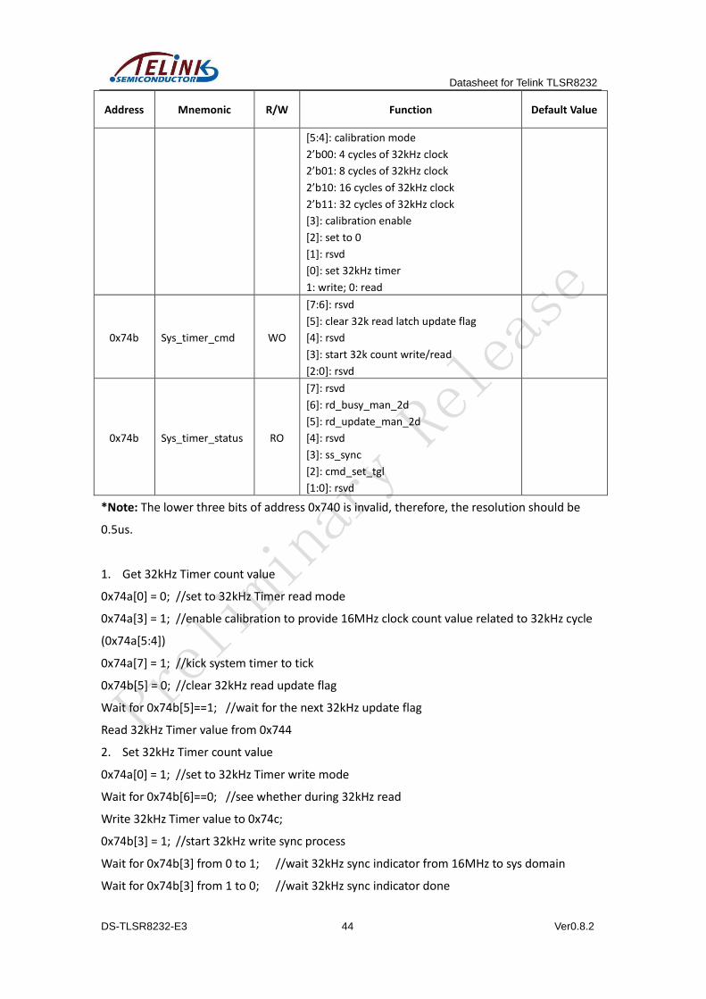
Datasheet for Telink TLSR8232
DS-TLSR8232-E3 44 Ver0.8.2
Address Mnemonic R/W Function Default Value
[5:4]: calibration mode
2’b00: 4 cycles of 32kHz clock
2’b01: 8 cycles of 32kHz clock
2’b10: 16 cycles of 32kHz clock
2’b11: 32 cycles of 32kHz clock
[3]: calibration enable
[2]: set to 0
[1]: rsvd
[0]: set 32kHz timer
1: write; 0: read
0x74b Sys_timer_cmd WO
[7:6]: rsvd
[5]: clear 32k read latch update flag
[4]: rsvd
[3]: start 32k count write/read
[2:0]: rsvd
0x74b Sys_timer_status RO
[7]: rsvd
[6]: rd_busy_man_2d
[5]: rd_update_man_2d
[4]: rsvd
[3]: ss_sync
[2]: cmd_set_tgl
[1:0]: rsvd
*Note: The lower three bits of address 0x740 is invalid, therefore, the resolution should be
0.5us.
1. Get 32kHz Timer count value
0x74a[0] = 0; //set to 32kHz Timer read mode
0x74a[3] = 1; //enable calibration to provide 16MHz clock count value related to 32kHz cycle
(0x74a[5:4])
0x74a[7] = 1; //kick system timer to tick
0x74b[5] = 0; //clear 32kHz read update flag
Wait for 0x74b[5]==1; //wait for the next 32kHz update flag
Read 32kHz Timer value from 0x744
2. Set 32kHz Timer count value
0x74a[0] = 1; //set to 32kHz Timer write mode
Wait for 0x74b[6]==0; //see whether during 32kHz read
Write 32kHz Timer value to 0x74c;
0x74b[3] = 1; //start 32kHz write sync process
Wait for 0x74b[3] from 0 to 1; //wait 32kHz sync indicator from 16MHz to sys domain
Wait for 0x74b[3] from 1 to 0; //wait 32kHz sync indicator done
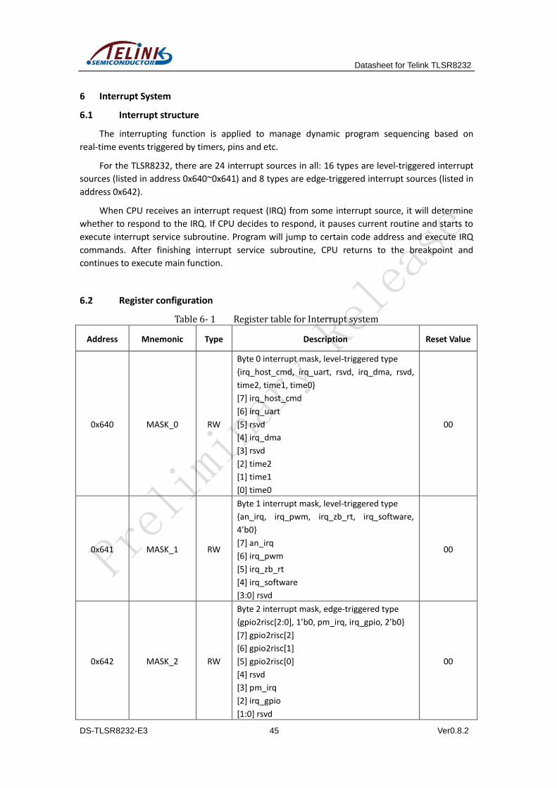
Datasheet for Telink TLSR8232
DS-TLSR8232-E3 45 Ver0.8.2
6 Interrupt System
6.1 Interrupt structure
The interrupting function is applied to manage dynamic program sequencing based on
real-time events triggered by timers, pins and etc.
For the TLSR8232, there are 24 interrupt sources in all: 16 types are level-triggered interrupt
sources (listed in address 0x640~0x641) and 8 types are edge-triggered interrupt sources (listed in
address 0x642).
When CPU receives an interrupt request (IRQ) from some interrupt source, it will determine
whether to respond to the IRQ. If CPU decides to respond, it pauses current routine and starts to
execute interrupt service subroutine. Program will jump to certain code address and execute IRQ
commands. After finishing interrupt service subroutine, CPU returns to the breakpoint and
continues to execute main function.
6.2 Register configuration
Table 6- 1 Register table for Interrupt system
Address Mnemonic Type Description Reset Value
0x640 MASK_0 RW
Byte 0 interrupt mask, level-triggered type
{irq_host_cmd, irq_uart, rsvd, irq_dma, rsvd,
time2, time1, time0}
[7] irq_host_cmd
[6] irq_uart
[5] rsvd
[4] irq_dma
[3] rsvd
[2] time2
[1] time1
[0] time0
00
0x641 MASK_1 RW
Byte 1 interrupt mask, level-triggered type
{an_irq, irq_pwm, irq_zb_rt, irq_software,
4’b0}
[7] an_irq
[6] irq_pwm
[5] irq_zb_rt
[4] irq_software
[3:0] rsvd
00
0x642 MASK_2 RW
Byte 2 interrupt mask, edge-triggered type
{gpio2risc[2:0], 1’b0, pm_irq, irq_gpio, 2’b0}
[7] gpio2risc[2]
[6] gpio2risc[1]
[5] gpio2risc[0]
[4] rsvd
[3] pm_irq
[2] irq_gpio
[1:0] rsvd
00
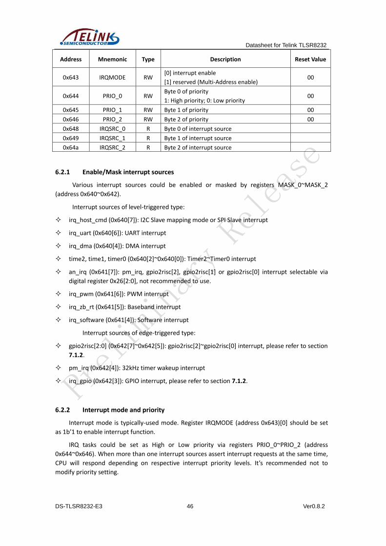
Datasheet for Telink TLSR8232
DS-TLSR8232-E3 46 Ver0.8.2
Address Mnemonic Type Description Reset Value
0x643 IRQMODE RW [0] interrupt enable
[1] reserved (Multi-Address enable) 00
0x644 PRIO_0 RW Byte 0 of priority
1: High priority; 0: Low priority 00
0x645 PRIO_1 RW Byte 1 of priority 00
0x646 PRIO_2 RW Byte 2 of priority 00
0x648 IRQSRC_0 R Byte 0 of interrupt source
0x649 IRQSRC_1 R Byte 1 of interrupt source
0x64a IRQSRC_2 R Byte 2 of interrupt source
6.2.1 Enable/Mask interrupt sources
Various interrupt sources could be enabled or masked by registers MASK_0~MASK_2
(address 0x640~0x642).
Interrupt sources of level-triggered type:
irq_host_cmd (0x640[7]): I2C Slave mapping mode or SPI Slave interrupt
irq_uart (0x640[6]): UART interrupt
irq_dma (0x640[4]): DMA interrupt
time2, time1, timer0 (0x640[2]~0x640[0]): Timer2~Timer0 interrupt
an_irq (0x641[7]): pm_irq, gpio2risc[2], gpio2risc[1] or gpio2risc[0] interrupt selectable via
digital register 0x26[2:0], not recommended to use.
irq_pwm (0x641[6]): PWM interrupt
irq_zb_rt (0x641[5]): Baseband interrupt
irq_software (0x641[4]): Software interrupt
Interrupt sources of edge-triggered type:
gpio2risc[2:0] (0x642[7]~0x642[5]): gpio2risc[2]~gpio2risc[0] interrupt, please refer to section
7.1.2.
pm_irq (0x642[4]): 32kHz timer wakeup interrupt
irq_gpio (0x642[3]): GPIO interrupt, please refer to section 7.1.2.
6.2.2 Interrupt mode and priority
Interrupt mode is typically-used mode. Register IRQMODE (address 0x643)[0] should be set
as 1b’1 to enable interrupt function.
IRQ tasks could be set as High or Low priority via registers PRIO_0~PRIO_2 (address
0x644~0x646). When more than one interrupt sources assert interrupt requests at the same time,
CPU will respond depending on respective interrupt priority levels. It’s recommended not to
modify priority setting.
Datasheet for Telink TLSR8232
DS-TLSR8232-E3 47 Ver0.8.2
6.2.3 Interrupt source flag
Three bytes in registers IRQSRC_0~IRQSRC_2 (address 0x648~0x64a) serve to indicate IRQ
sources. Once IRQ occurs from certain source, the corresponding IRQ source flag will be set as “1”.
User could identify IRQ source by reading address 0x648~0x64a.
When handling edge-triggered type interrupt, the corresponding IRQ source flag needs to be
cleared via address 0x64a. Take the interrupt source irq_gpio for example: First enable the
interrupt source by setting address 0x642 bit[2] as 1b’1; then set address 0x643 bit[0] as 1b’1 to
enable the interrupt. In interrupt handling function, 24-bit data is read from address 0x648~0x64a
to check which IRQ source is valid; if data bit[18] is 1, it means the irq_gpio IRQ source is valid.
Clear this interrupt source by setting address 0x64a bit[2] as 1b’1.
As for level-type interrupt, IRQ interrupt source status needs to be cleared via setting
corresponding module status register. Take Timer0 IRQ interrupt source for example: First enable
the interrupt source by setting address 0x640 bit[0] as 1b’1; then set address 0x643 bit[0] as 1b’1
to enable the interrupt. In interrupt handling function, 24-bit data is read from address
0x648~0x64a to check which IRQ source is valid; if data bit[0] is 1, it means the Timer0 IRQ source
is valid. Register TMR_STATUS (address 0x623) [0] should be written with 1b’1 to manually clear
Timer0 status (refer to section 5.1.1 Register table).
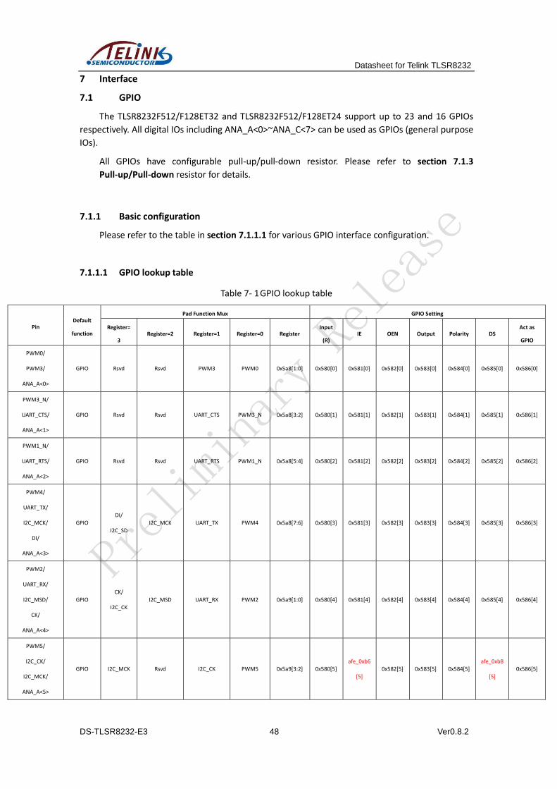
Datasheet for Telink TLSR8232
DS-TLSR8232-E3 48 Ver0.8.2
7 Interface
7.1 GPIO
The TLSR8232F512/F128ET32 and TLSR8232F512/F128ET24 support up to 23 and 16 GPIOs
respectively. All digital IOs including ANA_A<0>~ANA_C<7> can be used as GPIOs (general purpose
IOs).
All GPIOs have configurable pull-up/pull-down resistor. Please refer to section 7.1.3
Pull-up/Pull-down resistor for details.
7.1.1 Basic configuration
Please refer to the table in section 7.1.1.1 for various GPIO interface configuration.
7.1.1.1 GPIO lookup table
Table 7- 1 GPIO lookup table
Pin Default
function
Pad Function Mux GPIO Setting
Register=
3 Register=2 Register=1 Register=0 Register
Input
(R) IE OEN Output Polarity DS
Act as
GPIO
PWM0/
PWM3/
ANA_A<0>
GPIO Rsvd Rsvd PWM3 PWM0 0x5a8[1:0] 0x580[0] 0x581[0] 0x582[0] 0x583[0] 0x584[0] 0x585[0] 0x586[0]
PWM3_N/
UART_CTS/
ANA_A<1>
GPIO Rsvd Rsvd UART_CTS PWM3_N 0x5a8[3:2] 0x580[1] 0x581[1] 0x582[1] 0x583[1] 0x584[1] 0x585[1] 0x586[1]
PWM1_N/
UART_RTS/
ANA_A<2>
GPIO Rsvd Rsvd UART_RTS PWM1_N 0x5a8[5:4] 0x580[2] 0x581[2] 0x582[2] 0x583[2] 0x584[2] 0x585[2] 0x586[2]
PWM4/
UART_TX/
I2C_MCK/
DI/
ANA_A<3>
GPIO
DI/
I2C_SD
I2C_MCK UART_TX PWM4 0x5a8[7:6] 0x580[3] 0x581[3] 0x582[3] 0x583[3] 0x584[3] 0x585[3] 0x586[3]
PWM2/
UART_RX/
I2C_MSD/
CK/
ANA_A<4>
GPIO
CK/
I2C_CK
I2C_MSD UART_RX PWM2 0x5a9[1:0] 0x580[4] 0x581[4] 0x582[4] 0x583[4] 0x584[4] 0x585[4] 0x586[4]
PWM5/
I2C_CK/
I2C_MCK/
ANA_A<5>
GPIO I2C_MCK Rsvd I2C_CK PWM5 0x5a9[3:2] 0x580[5] afe_0xb6
[5]
0x582[5] 0x583[5] 0x584[5] afe_0xb8
[5]
0x586[5]
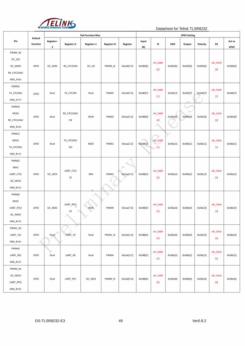
Datasheet for Telink TLSR8232
DS-TLSR8232-E3 49 Ver0.8.2
Pin Default
function
Pad Function Mux GPIO Setting
Register=
3 Register=2 Register=1 Register=0 Register
Input
(R) IE OEN Output Polarity DS
Act as
GPIO
PWM4_N/
I2C_SD/
I2C_MSD/
RX_CYC2LNA/
ANA_A<6>
GPIO I2C_MSD RX_CYC2LNA I2C_SD PWM4_N 0x5a9[5:4] 0x580[6]
afe_0xb6
[6]
0x582[6] 0x583[6] 0x584[6]
afe_0xb8
[6]
0x586[6]
PWM5/
TX_CYC2PA/
ANA_A<7>
GPIO Rsvd TX_CYC2PA Rsvd PWM5 0x5a9[7:6] 0x580[7] afe_0xb6
[7] 0x582[7] 0x583[7] 0x584[7]
afe_0xb8
[7] 0x586[7]
PWM3/
MCN/
RX_CYC2LNA/
ANA_B<0>
GPIO Rsvd
RX_CYC2LNA/
CN
MCN PWM3 0x5aa[1:0] 0x588[0]
afe_0xb9
[0]
0x58a[0] 0x58b[0] 0x58c[0]
afe_0xbb
[0]
0x58e[0]
PWM1/
MDO/
TX_CYC2PA/
ANA_B<1>
GPIO Rsvd
TX_CYC2PA/
DO
MDO PWM1 0x5aa[3:2] 0x588[1]
afe_0xb9
[1]
0x58a[1] 0x58b[1] 0x58c[1]
afe_0xbb
[1]
0x58e[1]
PWM2/
MDI/
UART_CTS/
I2C_MCK/
ANA_B<2>
GPIO I2C_MCK
UART_CTS/
DI
MDI PWM2 0x5aa[5:4] 0x588[2]
afe_0xb9
[2]
0x58a[2] 0x58b[2] 0x58c[2]
afe_0xbb
[2]
0x58e[2]
PWM0/
MCK/
UART_RTS/
I2C_MSD/
ANA_B<3>
GPIO I2C_MSD
UART_RTS/
CK
MCK PWM0 0x5aa[7:6] 0x588[3]
afe_0xb9
[3]
0x58a[3] 0x58b[3] 0x58c[3]
afe_0xbb
[3]
0x58e[3]
PWM1_N/
UART_TX/
ANA_B<4>
GPIO Rsvd UART_TX Rsvd PWM1_N 0x5ab[1:0] 0x588[4]
afe_0xb9
[4]
0x58a[4] 0x58b[4] 0x58c[4]
afe_0xbb
[4]
0x58e[4]
PWM4/
UART_RX/
ANA_B<5>
GPIO Rsvd UART_RX Rsvd PWM4 0x5ab[3:2] 0x588[5]
afe_0xb9
[5] 0x58a[5] 0x58b[5] 0x58c[5]
afe_0xbb
[5] 0x58e[5]
PWM0_N/
I2C_MCK/
UART_RTS/
ANA_B<6>
GPIO Rsvd UART_RTS I2C_MCK PWM0_N 0x5ab[5:4] 0x588[6]
afe_0xb9
[6]
0x58a[6] 0x58b[6] 0x58c[6]
afe_0xbb
[6]
0x58e[6]
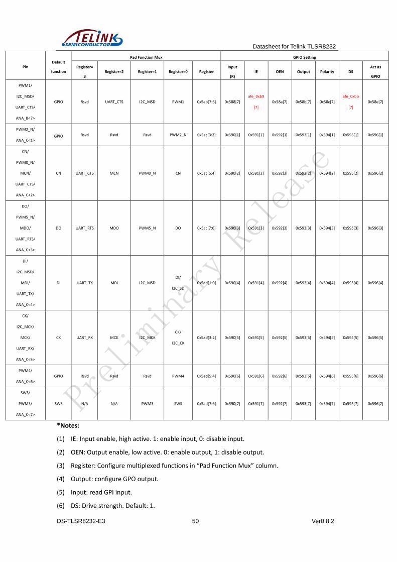
Datasheet for Telink TLSR8232
DS-TLSR8232-E3 50 Ver0.8.2
Pin Default
function
Pad Function Mux GPIO Setting
Register=
3 Register=2 Register=1 Register=0 Register
Input
(R) IE OEN Output Polarity DS
Act as
GPIO
PWM1/
I2C_MSD/
UART_CTS/
ANA_B<7>
GPIO Rsvd UART_CTS I2C_MSD PWM1 0x5ab[7:6] 0x588[7]
afe_0xb9
[7]
0x58a[7] 0x58b[7] 0x58c[7]
afe_0xbb
[7]
0x58e[7]
PWM2_N/
ANA_C<1> GPIO Rsvd Rsvd Rsvd PWM2_N 0x5ac[3:2] 0x590[1] 0x591[1] 0x592[1] 0x593[1] 0x594[1] 0x595[1] 0x596[1]
CN/
PWM0_N/
MCN/
UART_CTS/
ANA_C<2>
CN UART_CTS MCN PWM0_N CN 0x5ac[5:4] 0x590[2] 0x591[2] 0x592[2] 0x593[2] 0x594[2] 0x595[2] 0x596[2]
DO/
PWM5_N/
MDO/
UART_RTS/
ANA_C<3>
DO UART_RTS MDO PWM5_N DO 0x5ac[7:6] 0x590[3] 0x591[3] 0x592[3] 0x593[3] 0x594[3] 0x595[3] 0x596[3]
DI/
I2C_MSD/
MDI/
UART_TX/
ANA_C<4>
DI UART_TX MDI I2C_MSD
DI/
I2C_SD
0x5ad[1:0] 0x590[4] 0x591[4] 0x592[4] 0x593[4] 0x594[4] 0x595[4] 0x596[4]
CK/
I2C_MCK/
MCK/
UART_RX/
ANA_C<5>
CK UART_RX MCK I2C_MCK
CK/
I2C_CK
0x5ad[3:2] 0x590[5] 0x591[5] 0x592[5] 0x593[5] 0x594[5] 0x595[5] 0x596[5]
PWM4/
ANA_C<6>
GPIO Rsvd Rsvd Rsvd PWM4 0x5ad[5:4] 0x590[6] 0x591[6] 0x592[6] 0x593[6] 0x594[6] 0x595[6] 0x596[6]
SWS/
PWM3/
ANA_C<7>
SWS N/A N/A PWM3 SWS 0x5ad[7:6] 0x590[7] 0x591[7] 0x592[7] 0x593[7] 0x594[7] 0x595[7] 0x596[7]
*Notes:
(1) IE: Input enable, high active. 1: enable input, 0: disable input.
(2) OEN: Output enable, low active. 0: enable output, 1: disable output.
(3) Register: Configure multiplexed functions in “Pad Function Mux” column.
(4) Output: configure GPO output.
(5) Input: read GPI input.
(6) DS: Drive strength. Default: 1.
Datasheet for Telink TLSR8232
DS-TLSR8232-E3 51 Ver0.8.2
(7) Act as GPIO: enable (1) or disable (0) GPIO function.
(8) Polarity: see section 7.1.2 Connection relationship between GPIO and related modules.
(9) Default function: By default, ANA_C<2:5> are used as SPI Slave function, ANA_C<7> is used as
SWS function, while the other GPIOs are used as GPIO function.
(10) Priority: “Act as GPIO” has the highest priority. To configure as multiplexed function, disable
GPIO function first.
(11) For all unused GPIOs, corresponding “IE” must be set as 0.
(12) When SWS/ANA_C<7> “IE” is set as 1, this pin must be fixed as pull-up/pull-down state (float
state is not allowed).
(13) afe_0xb6, afe_0xb8, afe_0xb9 and afe_0xbb marked in red color are analog registers; others
are digital registers.
(14) Rsvd: reserved for internal debugging.
7.1.1.2 Multiplexed functions
Each pin listed in Table 7-1 acts as the function in the “Default Function” column by default.
By default, ANA_C<2:5> are used as SPI Slave function, ANA_C<7> is used as SWS function, while
the other GPIOs are used as GPIO function.
If a pin with multiplexed functions does not act as GPIO function by default, to use it as GPIO,
first set the bit in “Act as GPIO” column as 1b’1. After GPIO function is enabled, if the pin is used
as output, both the bits in “IE” and “OEN” columns should be set as 1b’0, then set the register
value in the “Output” column; if the pin is used as input, both the bits in “IE” and “OEN” columns
should be set as 1b’1, and the input data can be read from the register in the “Input” column.
To use a pin as certain multiplexed function (neither the default function nor GPIO function),
first clear the bit in “Act as GPIO” column to disable GPIO function, and then configure “Register”
in “Pad Function Mux” column to enable multiplexed function correspondingly.
Example 1: PWM0/PWM3/ ANA_A<0>.
(1) This pin acts as GPIO function by default.
To use this pin as general output, both address 0x581[0] (IE) and 0x582[0] (OEN) should be
set as 1b’0, then configure address 0x583[0] (Output).
To use this pin as general input, both address 0x581[0] (IE) and 0x582[0] (OEN) should be set
as 1b’1, and the input data can be read from address 0x580[0] (Input).
(2) To use this pin as PWM0 function, address 0x586[0] (Act as GPIO) should be set as 1b’0, and
0x5a8[1:0] (Register) should be set as 2b’00.
(3) To use this pin as PWM3 function, address 0x586[0] (Act as GPIO) should be set as 1b’0, and
0x5a8[1:0] (Register) should be set as 2b’01.
Example 2: CN/PWM0_N/MCN/UART_CTS/ANA_C<2>.
(1) This pin acts as SPI Slave CN function by default.
(2) To use this pin as GPIO function, first set address 0x596[2] (Act as GPIO) as 1b’1.
Datasheet for Telink TLSR8232
DS-TLSR8232-E3 52 Ver0.8.2
If the pin is used as general output, both address 0x591[2] (IE) and 0x592[2] (OEN) should be
set as 1b’0, then configure address 0x593[2] (Output).
If the pin is used as general input, both address 0x591[2] (IE) and 0x592[2] (OEN) should be
set to 1b’1, and the input data can be read from address 0x590[2] (Input).
(3) To use it as PWM0_N function, set address 0x596[2] (Act as GPIO) as 1b’0, and set 0x5ac[5:4]
(Register) to 2b’01.
(4) To use it as SPI Master MCN function, set address 0x596[2] (Act as GPIO) as 1b’0, and set
0x5ac[5:4] (Register) to 2b’10.
(5) To use it as UART_CTS function, set address 0x596[2] (Act as GPIO) as 1b’0, and set 0x5ac[5:4]
(Register) to 2b’11.
7.1.1.3 Drive strength
The registers in the “DS” column are used to configure the corresponding pin’s driving
strength: “1” indicates maximum drive level, while “0” indicates minimal drive level.
The “DS” configuration will take effect when the pin is used as output. It’s set as the strongest
driving level by default. In actual applications, driving strength can be decreased to lower level if
necessary.
ANA_A<0>~ANA_C<7>: maximum=8mA (“DS”=1), minimum=4mA (“DS”=0).
7.1.2 Connection relationship between GPIO and related modules
GPIO can be used to generate GPIO interrupt signal for interrupt system, counting or control
signal for Timer/Counter module, or GPIO2RISC interrupt signal for interrupt system.
For the “Exclusive Or (XOR)” operation result for input signal from any GPIO pin and
respective “Polarity” value, on one hand, it takes “And” operation with “irq” and generates GPIO
interrupt request signal; on the other hand, it takes “And” operation with “m0/m1/m2”, and
generates counting signal in Mode 1 or control signal in Mode 2 for Timer0/Timer1/Timer2, or
generates GPIO2RISC[0]/GPIO2RISC[1]/GPIO2RISC[2] interrupt request signal.
GPIO interrupt request signal = | ((input ^ polarity) & irq);
Counting (Mode 1) or control (Mode 2) signal for Timer0 = | ((input ^ polarity) & m0);
Counting (Mode 1) or control (Mode 2) signal for Timer1 = | ((input ^ polarity) & m1);
Counting (Mode 1) or control (Mode 2) signal for Timer2 = | ((input ^ polarity) & m2);
GPIO2RISC[0] interrupt request signal = | ((input ^ polarity) & m0);
GPIO2RISC[1] interrupt request signal = | ((input ^ polarity) & m1);
GPIO2RISC[2] interrupt request signal = | ((input ^ polarity) & m2).
Datasheet for Telink TLSR8232
DS-TLSR8232-E3 53 Ver0.8.2
Timer0
Timer1
Timer2
Input
Polarity
m1
m0
m2
Irq GPIO_IRQ
Timer0_IRQ
Timer1_IRQ
Timer2_IRQ
GPIO2RISC[2]_IRQ
GPIO2RISC[1]_IRQ
GPIO2RISC[0]_IRQ
Figure 7- 1 Logic relationship between GPIO and related modules
Please refer to Table 7- 2 and Table 6- 1 to learn how to configure GPIO for interrupt system
or Timer/Counter (Mode 1 or Mode 2).
(1) First enable GPIO function, enable IE and disable OEN. Please see section 7.1.1 Basic
configuration.
(2) GPIO IRQ signal:
Select GPIO interrupt trigger edge (positive edge or negative edge) via configuring “Polarity”,
and set corresponding GPIO interrupt enabling bit “Irq”.
Then set address 0x5b5[3] to enable GPIO IRQ.
Finally enable GPIO interrupt (irq_gpio) via MASK_2 (address 0x642[2]).
User can read addresses 0x5e0 ~ 0x5e2 to see which GPIO asserts GPIO interrupt request
signal. Note: 0x5e0[7:0] --> ANA_A<7>~ANA_A<0>, 0x5e1[7:0] --> ANA_B<7>~ANA_B<0>,
0x5e2[7:1] --> ANA_C<7>~ANA_C<1>.
(3) Timer/Counter counting or control signal:
Configure “Polarity”. In Timer Mode 1, it determines GPIO edge when Timer Tick counting
increases. In Timer Mode 2, it determines GPIO edge when Timer Tick starts counting.
Then set “m0/m1/m2” to specify the GPIO which generates counting signal (Mode 1)/control
signal (Mode 2) for Timer0/Timer1/Timer2.
User can read addresses 0x5e8~0x5ea/0x5f0~0x5f2/0x5f8~0x5fa to see which GPIO asserts
counting signal (in Mode 1) or control signal (in Mode 2) for Timer0/Timer1/Timer2. Note:
Timer0: 0x5e8[7:0] --> ANA_A<7>~ANA_A<0>, 0x5e9[7:0] --> ANA_B<7>~ANA_B<0>,
0x5ea[7:1] --> ANA_C<7>~ANA_C<1>; Timer1: 0x5f0[7:0] --> ANA_A<7>~ANA_A<0>,
Datasheet for Telink TLSR8232
DS-TLSR8232-E3 54 Ver0.8.2
0x5f1[7:0] --> ANA_B<7>~ANA_B<0>, 0x5f2[7:1] --> ANA_C<7>~ANA_C<1>; Timer2: 0x5f8[7:0]
--> ANA_A<7>~ANA_A<0>, 0x5f9[7:0] --> ANA_B<7>~ANA_B<0>, 0x5fa[7:1] -->
ANA_C<7>~ANA_C<1>.
(4) GPIO2RISC IRQ signal:
Select GPIO2RISC interrupt trigger edge (positive edge or negative edge) via configuring
“Polarity”, and set corresponding GPIO enabling bit “m0”/“m1”/“m2”.
Enable GPIO2RISC[0]/GPIO2RISC[1]/GPIO2RISC[2] interrupt via MASK_2, i.e. “gpio2risc[0]”
(address 0x642[5]) / “gpio2risc[1]” (address 0x642[6]) / “gpio2risc[2]” (address 0x642[7]).
Table 7- 2 GPIO lookup table2
Pin Input
(R)
Polarity
1: active low
0: active high
Irq m0 m1 m2
ANA_A<0> 0x580[0] 0x584[0] 0x587[0] 0x5b8[0] 0x5c0[0] 0x5c8[0]
ANA_A<1> 0x580[1] 0x584[1] 0x587[1] 0x5b8[1] 0x5c0[1] 0x5c8[1]
ANA_A<2> 0x580[2] 0x584[2] 0x587[2] 0x5b8[2] 0x5c0[2] 0x5c8[2]
ANA_A<3> 0x580[3] 0x584[3] 0x587[3] 0x5b8[3] 0x5c0[3] 0x5c8[3]
ANA_A<4> 0x580[4] 0x584[4] 0x587[4] 0x5b8[4] 0x5c0[4] 0x5c8[4]
ANA_A<5> 0x580[5] 0x584[5] 0x587[5] 0x5b8[5] 0x5c0[5] 0x5c8[5]
ANA_A<6> 0x580[6] 0x584[6] 0x587[6] 0x5b8[6] 0x5c0[6] 0x5c8[6]
ANA_A<7> 0x580[7] 0x584[7] 0x587[7] 0x5b8[7] 0x5c0[7] 0x5c8[7]
ANA_B<0> 0x588[0] 0x58c[0] 0x58f[0] 0x5b9[0] 0x5c1[0] 0x5c9[0]
ANA_B<1> 0x588[1] 0x58c[1] 0x58f[1] 0x5b9[1] 0x5c1[1] 0x5c9[1]
ANA_B<2> 0x588[2] 0x58c[2] 0x58f[2] 0x5b9[2] 0x5c1[2] 0x5c9[2]
ANA_B<3> 0x588[3] 0x58c[3] 0x58f[3] 0x5b9[3] 0x5c1[3] 0x5c9[3]
ANA_B<4> 0x588[4] 0x58c[4] 0x58f[4] 0x5b9[4] 0x5c1[4] 0x5c9[4]
ANA_B<5> 0x588[5] 0x58c[5] 0x58f[5] 0x5b9[5] 0x5c1[5] 0x5c9[5]
ANA_B<6> 0x588[6] 0x58c[6] 0x58f[6] 0x5b9[6] 0x5c1[6] 0x5c9[6]
ANA_B<7> 0x588[7] 0x58c[7] 0x58f[7] 0x5b9[7] 0x5c1[7] 0x5c9[7]
ANA_C<1> 0x590[1] 0x594[1] 0x597[1] 0x5ba[1] 0x5c2[1] 0x5ca[1]
ANA_C<2> 0x590[2] 0x594[2] 0x597[2] 0x5ba[2] 0x5c2[2] 0x5ca[2]
ANA_C<3> 0x590[3] 0x594[3] 0x597[3] 0x5ba[3] 0x5c2[3] 0x5ca[3]
ANA_C<4> 0x590[4] 0x594[4] 0x597[4] 0x5ba[4] 0x5c2[4] 0x5ca[4]
ANA_C<5> 0x590[5] 0x594[5] 0x597[5] 0x5ba[5] 0x5c2[5] 0x5ca[5]
ANA_C<6> 0x590[6] 0x594[6] 0x597[6] 0x5ba[6] 0x5c2[6] 0x5ca[6]
ANA_C<7> 0x590[7] 0x594[7] 0x597[7] 0x5ba[7] 0x5c2[7] 0x5ca[7]
Datasheet for Telink TLSR8232
DS-TLSR8232-E3 55 Ver0.8.2
7.1.3 Pull-up/Pull-down resistor
All GPIOs (including ANA_A<0>~ANA_C<7>) support configurable pull-up resistor of rank x1
and x100 or pull-down resistor of rank x10 which are all disabled by default. Analog registers
afe_0x08~afe_0x0d serve to control the pull-up/ pull-down resistor for each GPIO.
Please refer to Table 7- 3 for details.
Take the ANA_A<5> for example: Setting analog register afe_0x08<1:0> to
2b’01/2b’10/2b’11 is to respectively enable pull-up resistor of rank x100 / pull-up resistor of rank
x1 / pull-down resistor of rank x10 for ANA_A<5>; Clearing the two bits (default value) disables
pull-up and pull-down resistor for ANA_A<5>.
Table 7- 3 Analog registers for pull-up/pull-down resistor control
Address Mnemonic Default Description
Rank Nominal range
x1 8kohm~60kohm
x10 80kohm~600kohm
x100 500kohm~2Mohm
Note: Since all the pull-up and pull-down resistors are implemented via MOSFET in the circuit,
the corresponding absolute values may have large variation range at PVT (Process Voltage
Temperature).
afe_0x08<1:0> pullupdown_ctrl<1:0> 00
ANA_A<5> pull up/down control
00 – No pull up/down resistor
01 – x100 pull-up resistor
10 – x1 pull-up resistor
11 – x10 pull-down resistor
afe_0x08<3:2> pullupdown_ctrl<1:0> 00
ANA_A<6> pull up/down control
00 – No pull up/down resistor
01 – x100 pull-up resistor
10 – x1 pull-up resistor
11 – x10 pull-down resistor
afe_0x08<5:4> pullupdown_ctrl<1:0> 00
ANA_A<7> pull up/down control
00 – No pull up/down resistor
01 – x100 pull-up resistor
10 – x1 pull-up resistor
11 – x10 pull-down resistor
afe_0x08<7:6> pullupdown_ctrl<1:0> 00
ANA_B<0> pull up/down control
00 – No pull up/down resistor
01 – x100 pull-up resistor
10 – x1 pull-up resistor
11 – x10 pull-down resistor
afe_0x09<1:0> pullupdown_ctrl<1:0> 00
ANA_B<1> pull up/down control
00 – No pull up/down resistor
01 – x100 pull-up resistor
10 – x1 pull-up resistor
11 – x10 pull-down resistor
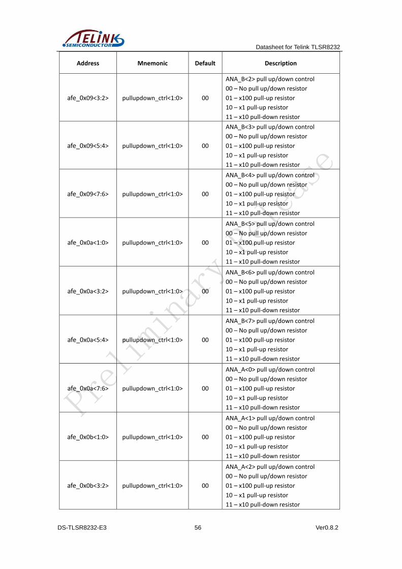
Datasheet for Telink TLSR8232
DS-TLSR8232-E3 56 Ver0.8.2
Address Mnemonic Default Description
afe_0x09<3:2> pullupdown_ctrl<1:0> 00
ANA_B<2> pull up/down control
00 – No pull up/down resistor
01 – x100 pull-up resistor
10 – x1 pull-up resistor
11 – x10 pull-down resistor
afe_0x09<5:4> pullupdown_ctrl<1:0> 00
ANA_B<3> pull up/down control
00 – No pull up/down resistor
01 – x100 pull-up resistor
10 – x1 pull-up resistor
11 – x10 pull-down resistor
afe_0x09<7:6> pullupdown_ctrl<1:0> 00
ANA_B<4> pull up/down control
00 – No pull up/down resistor
01 – x100 pull-up resistor
10 – x1 pull-up resistor
11 – x10 pull-down resistor
afe_0x0a<1:0> pullupdown_ctrl<1:0> 00
ANA_B<5> pull up/down control
00 – No pull up/down resistor
01 – x100 pull-up resistor
10 – x1 pull-up resistor
11 – x10 pull-down resistor
afe_0x0a<3:2> pullupdown_ctrl<1:0> 00
ANA_B<6> pull up/down control
00 – No pull up/down resistor
01 – x100 pull-up resistor
10 – x1 pull-up resistor
11 – x10 pull-down resistor
afe_0x0a<5:4> pullupdown_ctrl<1:0> 00
ANA_B<7> pull up/down control
00 – No pull up/down resistor
01 – x100 pull-up resistor
10 – x1 pull-up resistor
11 – x10 pull-down resistor
afe_0x0a<7:6> pullupdown_ctrl<1:0> 00
ANA_A<0> pull up/down control
00 – No pull up/down resistor
01 – x100 pull-up resistor
10 – x1 pull-up resistor
11 – x10 pull-down resistor
afe_0x0b<1:0> pullupdown_ctrl<1:0> 00
ANA_A<1> pull up/down control
00 – No pull up/down resistor
01 – x100 pull-up resistor
10 – x1 pull-up resistor
11 – x10 pull-down resistor
afe_0x0b<3:2> pullupdown_ctrl<1:0> 00
ANA_A<2> pull up/down control
00 – No pull up/down resistor
01 – x100 pull-up resistor
10 – x1 pull-up resistor
11 – x10 pull-down resistor
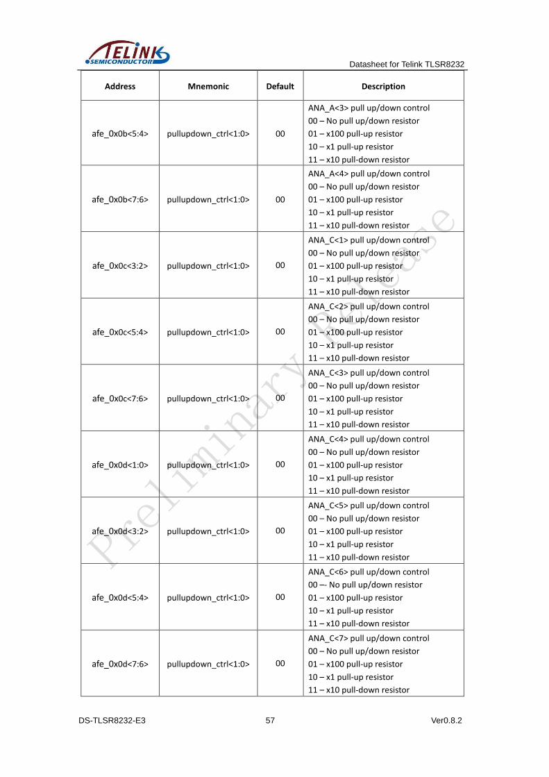
Datasheet for Telink TLSR8232
DS-TLSR8232-E3 57 Ver0.8.2
Address Mnemonic Default Description
afe_0x0b<5:4> pullupdown_ctrl<1:0> 00
ANA_A<3> pull up/down control
00 – No pull up/down resistor
01 – x100 pull-up resistor
10 – x1 pull-up resistor
11 – x10 pull-down resistor
afe_0x0b<7:6> pullupdown_ctrl<1:0> 00
ANA_A<4> pull up/down control
00 – No pull up/down resistor
01 – x100 pull-up resistor
10 – x1 pull-up resistor
11 – x10 pull-down resistor
afe_0x0c<3:2> pullupdown_ctrl<1:0> 00
ANA_C<1> pull up/down control
00 – No pull up/down resistor
01 – x100 pull-up resistor
10 – x1 pull-up resistor
11 – x10 pull-down resistor
afe_0x0c<5:4> pullupdown_ctrl<1:0> 00
ANA_C<2> pull up/down control
00 – No pull up/down resistor
01 – x100 pull-up resistor
10 – x1 pull-up resistor
11 – x10 pull-down resistor
afe_0x0c<7:6> pullupdown_ctrl<1:0> 00
ANA_C<3> pull up/down control
00 – No pull up/down resistor
01 – x100 pull-up resistor
10 – x1 pull-up resistor
11 – x10 pull-down resistor
afe_0x0d<1:0> pullupdown_ctrl<1:0> 00
ANA_C<4> pull up/down control
00 – No pull up/down resistor
01 – x100 pull-up resistor
10 – x1 pull-up resistor
11 – x10 pull-down resistor
afe_0x0d<3:2> pullupdown_ctrl<1:0> 00
ANA_C<5> pull up/down control
00 – No pull up/down resistor
01 – x100 pull-up resistor
10 – x1 pull-up resistor
11 – x10 pull-down resistor
afe_0x0d<5:4> pullupdown_ctrl<1:0> 00
ANA_C<6> pull up/down control
00 –- No pull up/down resistor
01 – x100 pull-up resistor
10 – x1 pull-up resistor
11 – x10 pull-down resistor
afe_0x0d<7:6> pullupdown_ctrl<1:0> 00
ANA_C<7> pull up/down control
00 – No pull up/down resistor
01 – x100 pull-up resistor
10 – x1 pull-up resistor
11 – x10 pull-down resistor
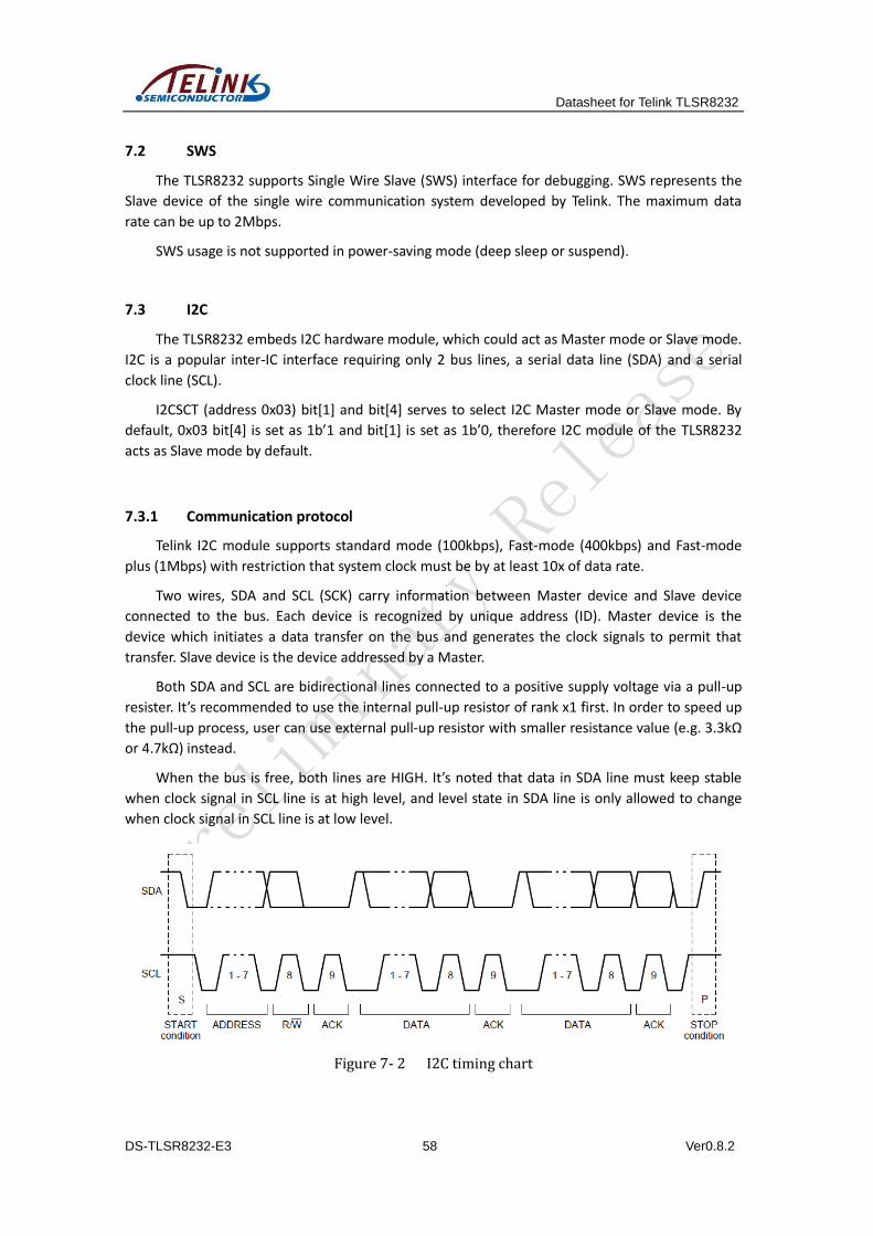
Datasheet for Telink TLSR8232
DS-TLSR8232-E3 58 Ver0.8.2
7.2 SWS
The TLSR8232 supports Single Wire Slave (SWS) interface for debugging. SWS represents the
Slave device of the single wire communication system developed by Telink. The maximum data
rate can be up to 2Mbps.
SWS usage is not supported in power-saving mode (deep sleep or suspend).
7.3 I2C
The TLSR8232 embeds I2C hardware module, which could act as Master mode or Slave mode.
I2C is a popular inter-IC interface requiring only 2 bus lines, a serial data line (SDA) and a serial
clock line (SCL).
I2CSCT (address 0x03) bit[1] and bit[4] serves to select I2C Master mode or Slave mode. By
default, 0x03 bit[4] is set as 1b’1 and bit[1] is set as 1b’0, therefore I2C module of the TLSR8232
acts as Slave mode by default.
7.3.1 Communication protocol
Telink I2C module supports standard mode (100kbps), Fast-mode (400kbps) and Fast-mode
plus (1Mbps) with restriction that system clock must be by at least 10x of data rate.
Two wires, SDA and SCL (SCK) carry information between Master device and Slave device
connected to the bus. Each device is recognized by unique address (ID). Master device is the
device which initiates a data transfer on the bus and generates the clock signals to permit that
transfer. Slave device is the device addressed by a Master.
Both SDA and SCL are bidirectional lines connected to a positive supply voltage via a pull-up
resister. It’s recommended to use the internal pull-up resistor of rank x1 first. In order to speed up
the pull-up process, user can use external pull-up resistor with smaller resistance value (e.g. 3.3kΩ
or 4.7kΩ) instead.
When the bus is free, both lines are HIGH. It’s noted that data in SDA line must keep stable
when clock signal in SCL line is at high level, and level state in SDA line is only allowed to change
when clock signal in SCL line is at low level.
Figure 7- 2 I2C timing chart
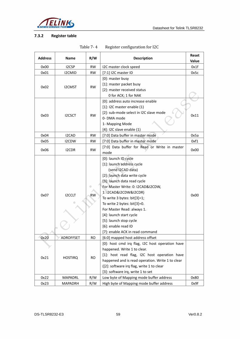
Datasheet for Telink TLSR8232
DS-TLSR8232-E3 59 Ver0.8.2
7.3.2 Register table
Table 7- 4 Register configuration for I2C
Address Name R/W Description Reset
Value
0x00 I2CSP RW I2C master clock speed 0x1f
0x01 I2CMID RW [7:1] I2C master ID 0x5c
0x02 I2CMST RW
[0]: master busy
[1]: master packet busy
[2]: master received status
0 for ACK; 1 for NAK
0x03 I2CSCT RW
[0]: address auto increase enable
[1]: I2C master enable (1)
[2]: sub-mode select in I2C slave mode
0- DMA mode
1- Mapping Mode
[4]: I2C slave enable (1)
0x11
0x04 I2CAD RW [7:0] Data buffer in master mode 0x5a
0x05 I2CDW RW [7:0] Data buffer in master mode 0xf1
0x06 I2CDR RW [7:0] Data buffer for Read or Write in master
mode 0x00
0x07 I2CCLT RW
[0]: launch ID cycle
[1]: launch address cycle
(send I2CAD data)
[2]: launch data write cycle
[3]: launch data read cycle
For Master Write: 0: I2CAD&I2CDW,
1: I2CAD&I2CDW&I2CDR)
To write 3 bytes: bit[3]=1;
To write 2 bytes: bit[3]=0.
For Master Read: always 1.
[4]: launch start cycle
[5]: launch stop cycle
[6]: enable read ID
[7]: enable ACK in read command
0x00
0x20 ADROFFSET RO [6:0] mapped host address offset
0x21 HOSTIRQ RO
[0]: host cmd irq flag, I2C host operation have
happened. Write 1 to clear.
[1]: host read flag, I2C host operation have
happened and is read operation. Write 1 to clear
([2]: software irq flag, write 1 to clear
[3]: software irq, write 1 to set
0x22 MAPADRL R/W Low byte of Mapping mode buffer address 0x80
0x23 MAPADRH R/W High byte of Mapping mode buffer address 0x9f
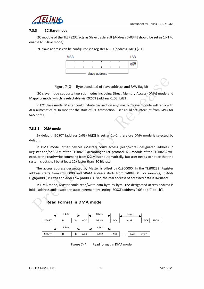
Datasheet for Telink TLSR8232
DS-TLSR8232-E3 60 Ver0.8.2
7.3.3 I2C Slave mode
I2C module of the TLSR8232 acts as Slave by default (Address 0x03[4] should be set as 1b’1 to
enable I2C Slave mode).
I2C slave address can be configured via register I2CID (address 0x01) [7:1].
Figure 7- 3 Byte consisted of slave address and R/W flag bit
I2C slave mode supports two sub modes including Direct Memory Access (DMA) mode and
Mapping mode, which is selectable via I2CSCT (address 0x03) bit[2].
In I2C Slave mode, Master could initiate transaction anytime. I2C slave module will reply with
ACK automatically. To monitor the start of I2C transaction, user could set interrupt from GPIO for
SCA or SCL.
7.3.3.1 DMA mode
By default, I2CSCT (address 0x03) bit[2] is set as 1b’0, therefore DMA mode is selected by
default.
In DMA mode, other devices (Master) could access (read/write) designated address in
Register and/or SRAM of the TLSR8232 according to I2C protocol. I2C module of the TLSR8232 will
execute the read/write command from I2C Master automatically. But user needs to notice that the
system clock shall be at least 10x faster than I2C bit rate.
The access address designated by Master is offset by 0x800000. In the TLSR8232, Register
address starts from 0x800000 and SRAM address starts from 0x808000. For example, if Addr
High(AddrH) is 0xaa and Addr Low (AddrL) is 0xcc, the real address of accessed data is 0x80aacc.
In DMA mode, Master could read/write data byte by byte. The designated access address is
initial address and it supports auto increment by setting I2CSCT (address 0x03) bit[0] to 1b’1.
START ID W
8 bits
ACK AddrH ACK AddrL ACK
DATA ACK
STOP
8 bits 8 bits
8 bits
Read Format in DMA mode
START ID R
8 bits
ACK NAK STOP
Figure 7- 4 Read format in DMA mode
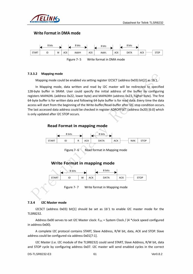
Datasheet for Telink TLSR8232
DS-TLSR8232-E3 61 Ver0.8.2
START ID W
8 bits
ACK AddrH ACK AddrL ACK DATA ACK STOP
8 bits 8 bits 8 bits
Write Format in DMA mode
Figure 7- 5 Write format in DMA mode
7.3.3.2 Mapping mode
Mapping mode could be enabled via setting register I2CSCT (address 0x03) bit[2] as 1b’1.
In Mapping mode, data written and read by I2C master will be redirected to specified
128-byte buffer in SRAM. User could specify the initial address of the buffer by configuring
registers MAPADRL (address 0x22, lower byte) and MAPADRH (address 0x23, higher byte). The first
64-byte buffer is for written data and following 64-byte buffer is for read data. Every time the data
access will start from the beginning of the Write-buffer/Read-buffer after I2C stop condition occurs.
The last accessed data address could be checked in register ADROFFSET (address 0x20) [6:0] which
is only updated after I2C STOP occurs.
DATA ACK
8 bits
Read Format in mapping mode
START ID R
8 bits
ACK NAK STOP
Figure 7- 6 Read format in Mapping mode
START ID W
8 bits
ACK DATA ACK STOP
8 bits
Write Format in mapping mode
Figure 7- 7 Write format in Mapping mode
7.3.4 I2C Master mode
I2CSCT (address 0x03) bit[1] should be set as 1b’1 to enable I2C master mode for the
TLSR8232.
Address 0x00 serves to set I2C Master clock: FI2C = System Clock / (4 *clock speed configured
in address 0x00).
A complete I2C protocol contains START, Slave Address, R/W bit, data, ACK and STOP. Slave
address could be configured via address 0x01[7:1].
I2C Master (i.e. I2C module of the TLSR8232) could send START, Slave Address, R/W bit, data
and STOP cycle by configuring address 0x07. I2C master will send enabled cycles in the correct
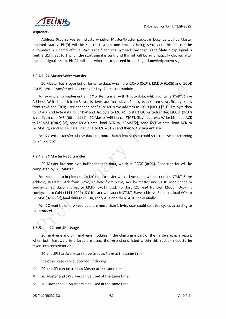
Datasheet for Telink TLSR8232
DS-TLSR8232-E3 62 Ver0.8.2
sequence.
Address 0x02 serves to indicate whether Master/Master packet is busy, as well as Master
received status. Bit[0] will be set to 1 when one byte is being sent, and this bit can be
automatically cleared after a start signal/ address byte/acknowledge signal/data /stop signal is
sent. Bit[1] is set to 1 when the start signal is sent, and this bit will be automatically cleared after
the stop signal is sent. Bit[2] indicates whether to succeed in sending acknowledgement signal.
7.3.4.1 I2C Master Write transfer
I2C Master has 3-byte buffer for write data, which are I2CAD (0x04), I2CDW (0x05) and I2CDR
(0x06). Write transfer will be completed by I2C master module.
For example, to implement an I2C write transfer with 3-byte data, which contains START, Slave
Address, Write bit, ack from Slave, 1st byte, ack from slave, 2nd byte, ack from slave, 3rd byte, ack
from slave and STOP, user needs to configure I2C slave address to I2CID (0x01) [7:1], 1st byte data
to I2CAD, 2nd byte data to I2CDW and 3rd byte to I2CDR. To start I2C write transfer, I2CCLT (0x07)
is configured to 0x3f (0011 1111). I2C Master will launch START, Slave address, Write bit, load ACK
to I2CMST (0x02) [2], send I2CAD data, load ACK to I2CMST[2], send I2CDW data, load ACK to
I2CMST[2], send I2CDR data, load ACK to I2CMST[2] and then STOP sequentially.
For I2C write transfer whose data are more than 3 bytes, user could split the cycles according
to I2C protocol.
7.3.4.2 I2C Master Read transfer
I2C Master has one byte buffer for read data, which is I2CDR (0x06). Read transfer will be
completed by I2C Master.
For example, to implement an I2C read transfer with 1 byte data, which contains START, Slave
Address, Read bit, Ack from Slave, 1st byte from Slave, Ack by master and STOP, user needs to
configure I2C slave address to I2CID (0x01) [7:1]. To start I2C read transfer, I2CCLT (0x07) is
configured to 0xf9 (1111 1001). I2C Master will launch START, Slave address, Read bit, load ACK to
I2CMST (0x02) [2], load data to I2CDR, reply ACK and then STOP sequentially.
For I2C read transfer whose data are more than 1 byte, user could split the cycles according to
I2C protocol.
7.3.5 I2C and SPI Usage
I2C hardware and SPI hardware modules in the chip share part of the hardware, as a result,
when both hardware interfaces are used, the restrictions listed within this section need to be
taken into consideration.
I2C and SPI hardware cannot be used as Slave at the same time.
The other cases are supported, including:
I2C and SPI can be used as Master at the same time.
I2C Master and SPI Slave can be used at the same time.
I2C Slave and SPI Master can be used at the same time.
Datasheet for Telink TLSR8232
DS-TLSR8232-E3 63 Ver0.8.2
7.4 SPI
The TLSR8232 embeds SPI (Serial Peripheral interface), which could act as Master mode or
Slave mode. SPI is a high-speed, full-duplex and synchronous communication bus requiring 4 bus
lines including a chip select (CS) line, a data input (DI) line, a data output (DO) line and a clock (CK)
line.
Register SPICT (address 0x09) bit[1] and bit[6] serve to select SPI Master mode or Slave mode.
By default, 0x09 bit[1] is set as 1b’0 and bit[6] is set as 1b’1, therefore SPI acts as Slave mode by
default.
7.4.1 Register table
Table 7- 5 Register configuration for SPI
Address Name R/W Description Reset Value
0x08 SPIDAT RW SPI data access 00
0x09 SPICT RW
[0]: p_csn
[1]: enable SPI master mode (1)
[2]: spi data output disable
[3]: 1 for read command; 0 for write
command
[4]: address auto increase
[5]: share_mode
[6]: enable SPI slave mode (1)
[7]: busy status
51
0x0a SPISP RW
[6:0]: SPI clock speed
[7]: SPI function mode, p_csn, p_scl,
p_sda and p_sdo function as SPI if 1
05
0x0b SPIMODE RW [0]: inverse SPI clock output
[1]: delay half clk for SPI data output 00
7.4.2 SPI Master mode
Address 0x09 bit[1] should be set as 1b’1 to enable SPI Master mode.
Register SPISP (address 0x0a) serves to configure SPI pin and clock: setting 0x0a bit[7] as 1b’1
is to enable SPI function mode, and corresponding pins can be used as SPI pins; SPI clock = system
clock/((clock speed configured in address 0x0a bit[6:0] +1)*2).
SPIDAT (address 0x08) serves as the data register. One reading/writing operation of 0x08
enables the SPI_CK pin to generate 8 SPI clock cycles.
Telink SPI supports four standard working modes: Mode 0~Mode 3. Register SPIMODE
(address 0x0b) serves to select one of the four SPI modes:

Datasheet for Telink TLSR8232
DS-TLSR8232-E3 64 Ver0.8.2
Table 7- 6 SPI mode
SPI mode CPOL/CPHA SPIMODE register
(Address 0x0b)
Mode 0 CPOL=0, CPHA=0 bit[0]=0, bit[1]=0
Mode 1 CPOL=0, CPHA=1 bit[0]=0, bit[1]=1
Mode 2 CPOL=1, CPHA=0 bit[0]=1, bit[1]=0
Mode 3 CPOL=1, CPHA=1 bit[0]=1, bit[1]=1
CPOL: Clock Polarity
When CPOL=0, SPI_CLK keeps low level in idle state;
When CPOL=1, SPI_CLK keeps high level in idle state.
CPHA: Clock Phase
When CPHA=0, data is sampled at the first edge of clock period
When CPHA=1, data is sampled at the latter edge of clock period
Address 0x09 bit[0] serves to control the CS line: when the bit is set to 1, the CS level is high;
when the bit is cleared, the CS level is low.
Address 0x09 bit[2] is the disabling bit for SPI Master output. When the bit is cleared, MCU
writes data into address 0x08, then the SPI_DO pin outputs the data bit by bit during the 8 clock
cycles generated by the SPI_CK pin. When the bit is set to 1b’1, SPI_DO output is disabled.
Address 0x09 bit[3] is the enabling bit for SPI Master reading data function. When the bit is
set to 1b’1, MCU reads the data from address 0x08, then the input data from the SPI_DI pin is
shifted into address 0x08 during the 8 clock cycles generated by the SPI_CK pin. When the bit is
cleared, SPI Master reading function is disabled.
Address 0x09[5] is the enabling bit for share mode, i.e. whether SPI_DI and SPI_DO share
one common line.
Users can read address 0x09 bit[7] to get SPI busy status, i.e. whether the 8 clock pulses have
been sent.
7.4.3 SPI Slave mode
SPI for the TLSR8232 acts as Slave mode by default. (Address 0x09 bit[6] should be set as 1b’1
to enable SPI Slave mode.)
SPI Slave mode supports DMA. User could access registers of the TLSR8232 by SPI interface.
It’s noted that system clock of TLSR8232 shall be at least 5x faster than SPI clock for reliable
connection. Address 0x0a should be written with data 0xa5 by the SPI host to activate SPI Slave
mode.
Address 0x09[4] is dedicated for SPI Slave mode and indicates address auto increment. SPI
write command format and read command format are illustrated in Figure 7-8:
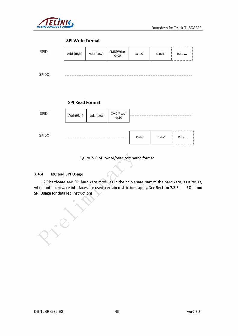
Datasheet for Telink TLSR8232
DS-TLSR8232-E3 65 Ver0.8.2
Figure 7- 8 SPI write/read command format
7.4.4 I2C and SPI Usage
I2C hardware and SPI hardware modules in the chip share part of the hardware, as a result,
when both hardware interfaces are used, certain restrictions apply. See Section 7.3.5 I2C and
SPI Usage for detailed instructions.
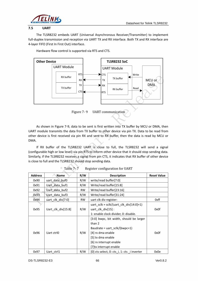
Datasheet for Telink TLSR8232
DS-TLSR8232-E3 66 Ver0.8.2
7.5 UART
The TLSR8232 embeds UART (Universal Asynchronous Receiver/Transmitter) to implement
full-duplex transmission and reception via UART TX and RX interface. Both TX and RX interface are
4-layer FIFO (First In First Out) interface.
Hardware flow control is supported via RTS and CTS.
RTS
TX
RX
CTS
MCU or DMA
Write
Read
TLSR8232 SoC
RX
RTS
TX
CTS
Other Device
RX buffer
TX buffer
UART Module
TX buffer
RX buffer
UART Module
Figure 7- 9 UART communication
As shown in Figure 7-9, data to be sent is first written into TX buffer by MCU or DMA, then
UART module transmits the data from TX buffer to other device via pin TX. Data to be read from
other device is first received via pin RX and sent to RX buffer, then the data is read by MCU or
DMA.
If RX buffer of the TLSR8232 UART is close to full, the TLSR8232 will send a signal
(configurable high or low level) via pin RTS to inform other device that it should stop sending data.
Similarly, if the TLSR8232 receives a signal from pin CTS, it indicates that RX buffer of other device
is close to full and the TLSR8232 should stop sending data.
Table 7- 7 Register configuration for UART
Address Name R/W Description Reset Value
0x90 uart_data_buf0 R/W write/read buffer[7:0]
0x91 Uart_data_buf1 R/W Write/read buffer[15:8]
0x92 Uart_data_buf2 RW Write/read buffer[23:16]
0x93 Uart_data_buf3 R/W Write/read buffer[31:24]
0x94 uart_clk_div[7:0] RW uart clk div register: 0xff
0x95 Uart_clk_div[15:8] R/W
uart_sclk = sclk/(uart_clk_div[14:0]+1)
uart_clk_div[15] :
1: enable clock divider, 0: disable.
0x0f
0x96 Uart ctrl0 R/W
[3:0] bwpc, bit width, should be larger
than 2
Baudrate = uart_sclk/(bwpc+1)
[4] rx dma enable
[5] tx dma enable
[6] rx interrupt enable
[7]tx interrupt enable
0x0f
0x97 Uart_ctrl1 R/W [0] cts select, 0: cts_i, 1: cts _i inverter 0x0e
Datasheet for Telink TLSR8232
DS-TLSR8232-E3 67 Ver0.8.2
Address Name R/W Description Reset Value
[1]:cts enable, 1: enable, 0, disable
[2]:Parity, 1: enable, 0 :disable
[3]: even Parity or odd
[5:4]: stop bit
00: 1 bit, 01, 1.5bit 1x: 2bits
[6]: ttl
[7]: uart tx, rx loopback
0x98 Uart_ctrl2 R/W
[3:0] rts trig level
[4] rts Parity
[5] rts manual value
[6] rts manual enable
[7] rts enable
0xa5
0x99 Uart_ctrl3 R/W [3:0]: rx_irq_trig level
[7:4] tx_irq_trig level 0x44
0x9a R_rxtimeout_o[7:0] R/W
The setting is transfer one bytes need
cycles base on uart_clk. For example, if
transfer one bytes (1 start bit+8bits
data+1 priority bit+2 stop bits) total 12
bits, this register setting should be
(bwpc+1)*12.
0x0f
0x9b R_rxtimeout_o[9:8] R/W
2’b00:rx timeout time is
r_rxtimeout[7:0]
2’b01:rx timeout time is
r_rxtimeout[7:0]*2
2’b10:rx timeout time is
r_rxtimeout[7:0]*3
3’b11: rx timeout time is
r_rxtimeout[7:0]*4
R_rxtimeout is for rx dma to decide the
end of each transaction. Supposed the
interval between each byte in one
transaction is very short.
0x00
0x9c Buf_cnt R [3:0]: r_buf_cnt
[7:4]: t_buf_cnt
0x9d Uart_sts R
[2:0] rbcnt
[3] irq
[6:4]wbcnt
[6] write 1 clear rx
[7] rx_err, write 1 clear tx
Addresses 0x90~0x93 serve to write data into TX buffer or read data from RX buffer.
Addresses 0x94~0x95 serve to configure UART clock.
Address 0x96 serves to set baud rate (bit[3:0]), enable RX/TX DMA mode (bit[4:5]), and
enable RX/TX interrupt (bit[6:7]).
Address 0x97 mainly serves to configure CTS. Bit[1] should be set to 1b’1 to enable CTS. Bit[0]
serves to configure CTS signal level. Bit[2:3] serve to enable parity bit and select even/odd parity.
Datasheet for Telink TLSR8232
DS-TLSR8232-E3 68 Ver0.8.2
Bit[5:4] serve to select 1/1.5/2 bits for stop bit. Bit[6] serves to configure whether RX/TX level
should be inverted.
Address 0x98 serves to configure RTS. Bit[7] and Bit[3:0] serve to enable RTS and configure
RTS signal level.
Address 0x99 serves to configure the number of bytes in RX/TX buffer to trigger interrupt.
The number of bytes in RX/TX buffer can be read from address 0x9c.
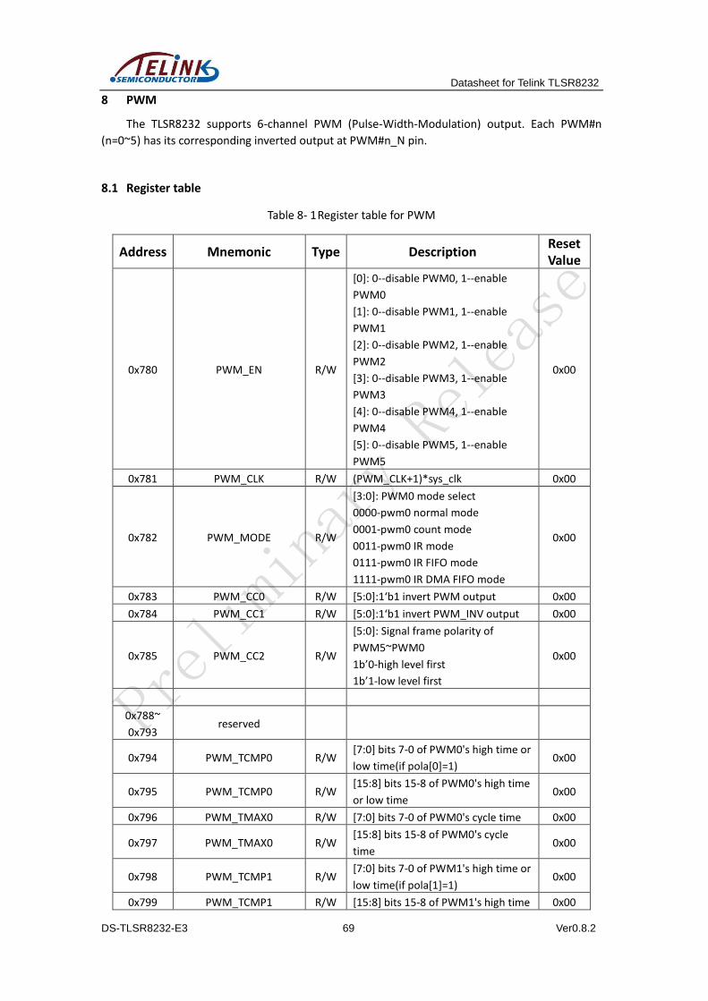
Datasheet for Telink TLSR8232
DS-TLSR8232-E3 69 Ver0.8.2
8 PWM
The TLSR8232 supports 6-channel PWM (Pulse-Width-Modulation) output. Each PWM#n
(n=0~5) has its corresponding inverted output at PWM#n_N pin.
8.1 Register table
Table 8- 1 Register table for PWM
Address Mnemonic Type Description Reset Value
0x780 PWM_EN R/W
[0]: 0--disable PWM0, 1--enable
PWM0
[1]: 0--disable PWM1, 1--enable
PWM1
[2]: 0--disable PWM2, 1--enable
PWM2
[3]: 0--disable PWM3, 1--enable
PWM3
[4]: 0--disable PWM4, 1--enable
PWM4
[5]: 0--disable PWM5, 1--enable
PWM5
0x00
0x781 PWM_CLK R/W (PWM_CLK+1)*sys_clk 0x00
0x782 PWM_MODE R/W
[3:0]: PWM0 mode select
0000-pwm0 normal mode
0001-pwm0 count mode
0011-pwm0 IR mode
0111-pwm0 IR FIFO mode
1111-pwm0 IR DMA FIFO mode
0x00
0x783 PWM_CC0 R/W [5:0]:1‘b1 invert PWM output 0x00
0x784 PWM_CC1 R/W [5:0]:1‘b1 invert PWM_INV output 0x00
0x785 PWM_CC2 R/W
[5:0]: Signal frame polarity of
PWM5~PWM0
1b’0-high level first
1b’1-low level first
0x00
0x788~
0x793 reserved
0x794 PWM_TCMP0 R/W [7:0] bits 7-0 of PWM0's high time or
low time(if pola[0]=1) 0x00
0x795 PWM_TCMP0 R/W [15:8] bits 15-8 of PWM0's high time
or low time 0x00
0x796 PWM_TMAX0 R/W [7:0] bits 7-0 of PWM0's cycle time 0x00
0x797 PWM_TMAX0 R/W [15:8] bits 15-8 of PWM0's cycle
time 0x00
0x798 PWM_TCMP1 R/W [7:0] bits 7-0 of PWM1's high time or
low time(if pola[1]=1) 0x00
0x799 PWM_TCMP1 R/W [15:8] bits 15-8 of PWM1's high time 0x00
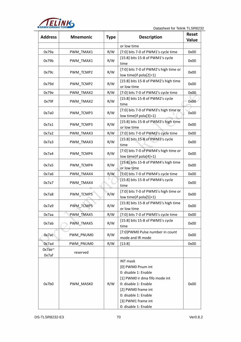
Datasheet for Telink TLSR8232
DS-TLSR8232-E3 70 Ver0.8.2
Address Mnemonic Type Description Reset Value
or low time
0x79a PWM_TMAX1 R/W [7:0] bits 7-0 of PWM1's cycle time 0x00
0x79b PWM_TMAX1 R/W [15:8] bits 15-8 of PWM1's cycle
time 0x00
0x79c PWM_TCMP2 R/W [7:0] bits 7-0 of PWM2's high time or
low time(if pola[2]=1) 0x00
0x79d PWM_TCMP2 R/W [15:8] bits 15-8 of PWM2's high time
or low time 0x00
0x79e PWM_TMAX2 R/W [7:0] bits 7-0 of PWM2's cycle time 0x00
0x79f PWM_TMAX2 R/W [15:8] bits 15-8 of PWM2's cycle
time 0x00
0x7a0 PWM_TCMP3 R/W [7:0] bits 7-0 of PWM3's high time or
low time(if pola[3]=1) 0x00
0x7a1 PWM_TCMP3 R/W [15:8] bits 15-8 of PWM3's high time
or low time 0x00
0x7a2 PWM_TMAX3 R/W [7:0] bits 7-0 of PWM3's cycle time 0x00
0x7a3 PWM_TMAX3 R/W [15:8] bits 15-8 of PWM3's cycle
time 0x00
0x7a4 PWM_TCMP4 R/W [7:0] bits 7-0 of PWM4's high time or
low time(if pola[4]=1) 0x00
0x7a5 PWM_TCMP4 R/W [15:8] bits 15-8 of PWM4's high time
or low time 0x00
0x7a6 PWM_TMAX4 R/W [7:0] bits 7-0 of PWM4's cycle time 0x00
0x7a7 PWM_TMAX4 [15:8] bits 15-8 of PWM4's cycle
time 0x00
0x7a8 PWM_TCMP5 R/W [7:0] bits 7-0 of PWM5's high time or
low time(if pola[5]=1) 0x00
0x7a9 PWM_TCMP5 R/W [15:8] bits 15-8 of PWM5's high time
or low time 0x00
0x7aa PWM_TMAX5 R/W [7:0] bits 7-0 of PWM5's cycle time 0x00
0x7ab PWM_TMAX5 R/W [15:8] bits 15-8 of PWM5's cycle
time 0x00
0x7ac PWM_PNUM0 R/W [7:0]PWM0 Pulse number in count
mode and IR mode 0x00
0x7ad PWM_PNUM0 R/W [13:8] 0x00
0x7ae~
0x7af reserved
0x7b0 PWM_MASK0 R/W
INT mask
[0] PWM0 Pnum int
0: disable 1: Enable
[1] PWM0 ir dma fifo mode int
0: disable 1: Enable
[2] PWM0 frame int
0: disable 1: Enable
[3] PWM1 frame int
0: disable 1: Enable
0x00
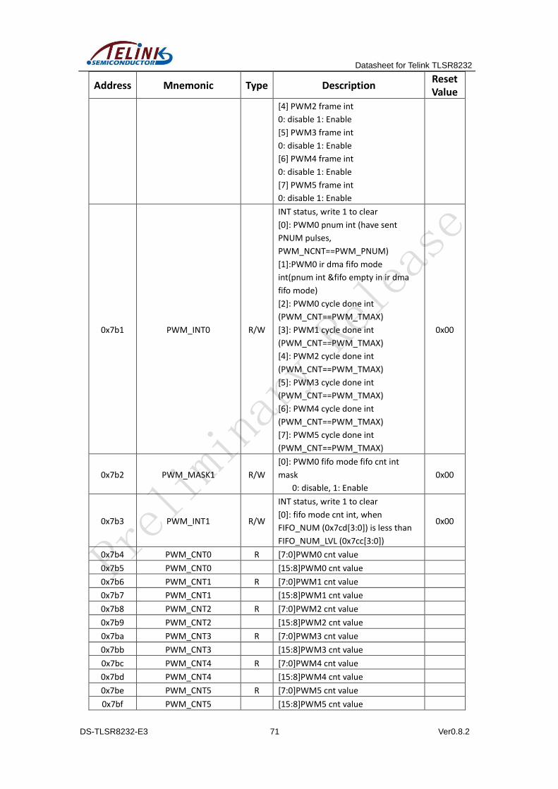
Datasheet for Telink TLSR8232
DS-TLSR8232-E3 71 Ver0.8.2
Address Mnemonic Type Description Reset Value
[4] PWM2 frame int
0: disable 1: Enable
[5] PWM3 frame int
0: disable 1: Enable
[6] PWM4 frame int
0: disable 1: Enable
[7] PWM5 frame int
0: disable 1: Enable
0x7b1 PWM_INT0 R/W
INT status, write 1 to clear
[0]: PWM0 pnum int (have sent
PNUM pulses,
PWM_NCNT==PWM_PNUM)
[1]:PWM0 ir dma fifo mode
int(pnum int &fifo empty in ir dma
fifo mode)
[2]: PWM0 cycle done int
(PWM_CNT==PWM_TMAX)
[3]: PWM1 cycle done int
(PWM_CNT==PWM_TMAX)
[4]: PWM2 cycle done int
(PWM_CNT==PWM_TMAX)
[5]: PWM3 cycle done int
(PWM_CNT==PWM_TMAX)
[6]: PWM4 cycle done int
(PWM_CNT==PWM_TMAX)
[7]: PWM5 cycle done int
(PWM_CNT==PWM_TMAX)
0x00
0x7b2 PWM_MASK1 R/W
[0]: PWM0 fifo mode fifo cnt int
mask
0: disable, 1: Enable
0x00
0x7b3 PWM_INT1 R/W
INT status, write 1 to clear
[0]: fifo mode cnt int, when
FIFO_NUM (0x7cd[3:0]) is less than
FIFO_NUM_LVL (0x7cc[3:0])
0x00
0x7b4 PWM_CNT0 R [7:0]PWM0 cnt value
0x7b5 PWM_CNT0 [15:8]PWM0 cnt value
0x7b6 PWM_CNT1 R [7:0]PWM1 cnt value
0x7b7 PWM_CNT1 [15:8]PWM1 cnt value
0x7b8 PWM_CNT2 R [7:0]PWM2 cnt value
0x7b9 PWM_CNT2 [15:8]PWM2 cnt value
0x7ba PWM_CNT3 R [7:0]PWM3 cnt value
0x7bb PWM_CNT3 [15:8]PWM3 cnt value
0x7bc PWM_CNT4 R [7:0]PWM4 cnt value
0x7bd PWM_CNT4 [15:8]PWM4 cnt value
0x7be PWM_CNT5 R [7:0]PWM5 cnt value
0x7bf PWM_CNT5 [15:8]PWM5 cnt value
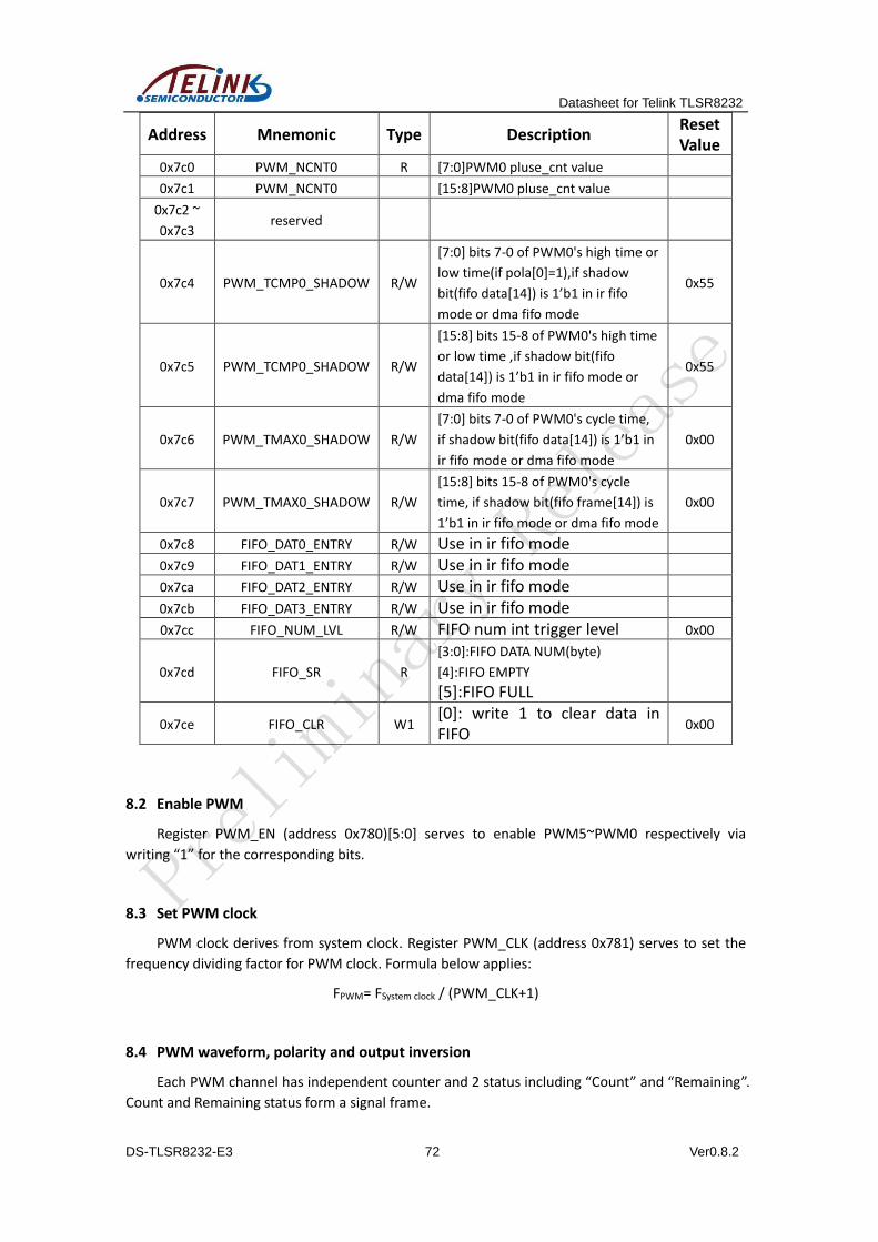
Datasheet for Telink TLSR8232
DS-TLSR8232-E3 72 Ver0.8.2
Address Mnemonic Type Description Reset Value
0x7c0 PWM_NCNT0 R [7:0]PWM0 pluse_cnt value
0x7c1 PWM_NCNT0 [15:8]PWM0 pluse_cnt value
0x7c2 ~
0x7c3 reserved
0x7c4 PWM_TCMP0_SHADOW R/W
[7:0] bits 7-0 of PWM0's high time or
low time(if pola[0]=1),if shadow
bit(fifo data[14]) is 1’b1 in ir fifo
mode or dma fifo mode
0x55
0x7c5 PWM_TCMP0_SHADOW R/W
[15:8] bits 15-8 of PWM0's high time
or low time ,if shadow bit(fifo
data[14]) is 1’b1 in ir fifo mode or
dma fifo mode
0x55
0x7c6 PWM_TMAX0_SHADOW R/W
[7:0] bits 7-0 of PWM0's cycle time,
if shadow bit(fifo data[14]) is 1’b1 in
ir fifo mode or dma fifo mode
0x00
0x7c7 PWM_TMAX0_SHADOW R/W
[15:8] bits 15-8 of PWM0's cycle
time, if shadow bit(fifo frame[14]) is
1’b1 in ir fifo mode or dma fifo mode
0x00
0x7c8 FIFO_DAT0_ENTRY R/W Use in ir fifo mode
0x7c9 FIFO_DAT1_ENTRY R/W Use in ir fifo mode
0x7ca FIFO_DAT2_ENTRY R/W Use in ir fifo mode
0x7cb FIFO_DAT3_ENTRY R/W Use in ir fifo mode
0x7cc FIFO_NUM_LVL R/W FIFO num int trigger level 0x00
0x7cd FIFO_SR R
[3:0]:FIFO DATA NUM(byte)
[4]:FIFO EMPTY
[5]:FIFO FULL
0x7ce FIFO_CLR W1 [0]: write 1 to clear data in FIFO
0x00
8.2 Enable PWM
Register PWM_EN (address 0x780)[5:0] serves to enable PWM5~PWM0 respectively via
writing “1” for the corresponding bits.
8.3 Set PWM clock
PWM clock derives from system clock. Register PWM_CLK (address 0x781) serves to set the
frequency dividing factor for PWM clock. Formula below applies:
FPWM= FSystem clock / (PWM_CLK+1)
8.4 PWM waveform, polarity and output inversion
Each PWM channel has independent counter and 2 status including “Count” and “Remaining”.
Count and Remaining status form a signal frame.
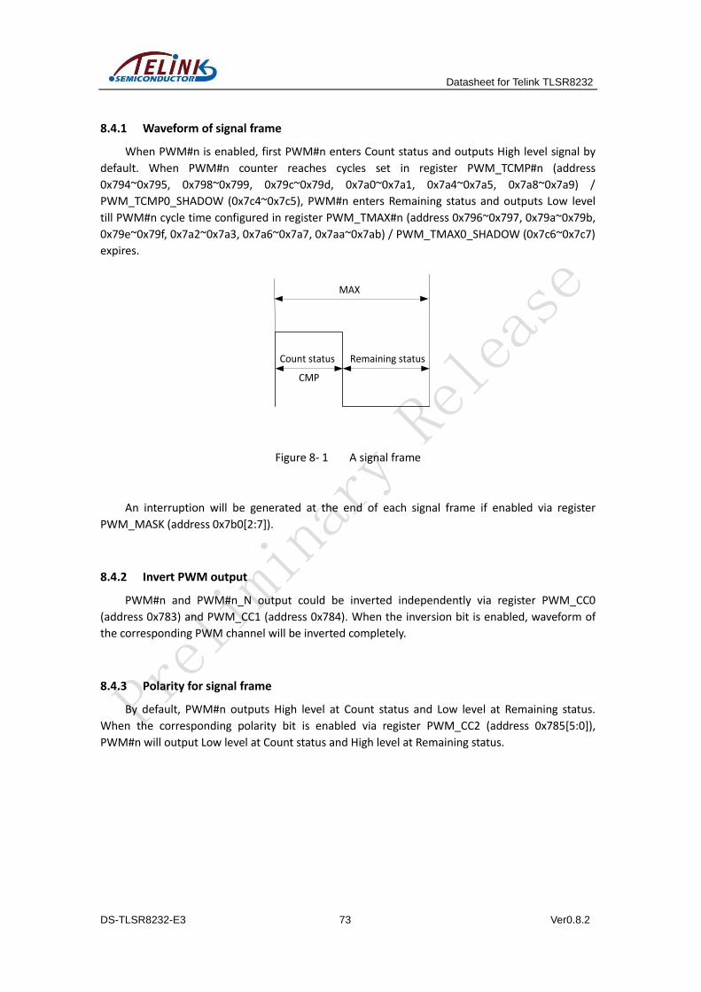
Datasheet for Telink TLSR8232
DS-TLSR8232-E3 73 Ver0.8.2
8.4.1 Waveform of signal frame
When PWM#n is enabled, first PWM#n enters Count status and outputs High level signal by
default. When PWM#n counter reaches cycles set in register PWM_TCMP#n (address
0x794~0x795, 0x798~0x799, 0x79c~0x79d, 0x7a0~0x7a1, 0x7a4~0x7a5, 0x7a8~0x7a9) /
PWM_TCMP0_SHADOW (0x7c4~0x7c5), PWM#n enters Remaining status and outputs Low level
till PWM#n cycle time configured in register PWM_TMAX#n (address 0x796~0x797, 0x79a~0x79b,
0x79e~0x79f, 0x7a2~0x7a3, 0x7a6~0x7a7, 0x7aa~0x7ab) / PWM_TMAX0_SHADOW (0x7c6~0x7c7)
expires.
CMP
MAX
Remaining statusCount status
Figure 8- 1 A signal frame
An interruption will be generated at the end of each signal frame if enabled via register
PWM_MASK (address 0x7b0[2:7]).
8.4.2 Invert PWM output
PWM#n and PWM#n_N output could be inverted independently via register PWM_CC0
(address 0x783) and PWM_CC1 (address 0x784). When the inversion bit is enabled, waveform of
the corresponding PWM channel will be inverted completely.
8.4.3 Polarity for signal frame
By default, PWM#n outputs High level at Count status and Low level at Remaining status.
When the corresponding polarity bit is enabled via register PWM_CC2 (address 0x785[5:0]),
PWM#n will output Low level at Count status and High level at Remaining status.
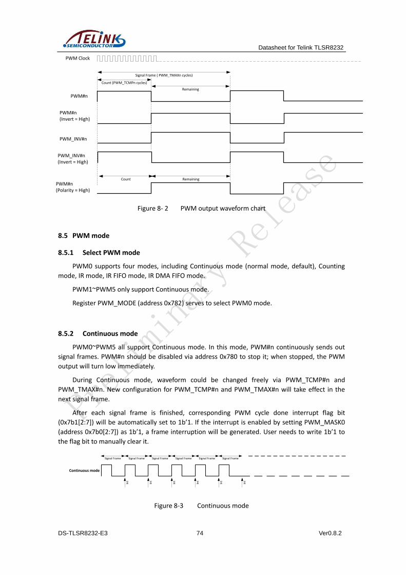
Datasheet for Telink TLSR8232
DS-TLSR8232-E3 74 Ver0.8.2
PWM#n
Signal Frame ( PWM_TMAXn cycles)
PWM#n (Invert = High)
PWM Clock
PWM_INV#n
PWM_INV#n (Invert = High)
Count Remaining
PWM#n(Polarity = High)
Count (PWM_TCMPn cycles)
Remaining
Figure 8- 2 PWM output waveform chart
8.5 PWM mode
8.5.1 Select PWM mode
PWM0 supports four modes, including Continuous mode (normal mode, default), Counting
mode, IR mode, IR FIFO mode, IR DMA FIFO mode.
PWM1~PWM5 only support Continuous mode.
Register PWM_MODE (address 0x782) serves to select PWM0 mode.
8.5.2 Continuous mode
PWM0~PWM5 all support Continuous mode. In this mode, PWM#n continuously sends out
signal frames. PWM#n should be disabled via address 0x780 to stop it; when stopped, the PWM
output will turn low immediately.
During Continuous mode, waveform could be changed freely via PWM_TCMP#n and
PWM_TMAX#n. New configuration for PWM_TCMP#n and PWM_TMAX#n will take effect in the
next signal frame.
After each signal frame is finished, corresponding PWM cycle done interrupt flag bit
(0x7b1[2:7]) will be automatically set to 1b’1. If the interrupt is enabled by setting PWM_MASK0
(address 0x7b0[2:7]) as 1b’1, a frame interruption will be generated. User needs to write 1b’1 to
the flag bit to manually clear it.
Continuous mode
Int
Int
Int
Int
Int
Int
Signal Frame Signal Frame Signal Frame Signal Frame Signal Frame Signal Frame
Figure 8-3 Continuous mode
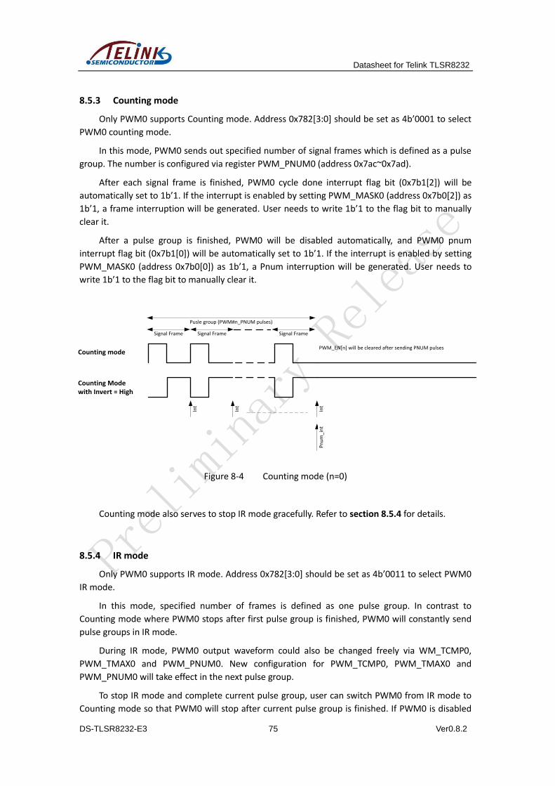
Datasheet for Telink TLSR8232
DS-TLSR8232-E3 75 Ver0.8.2
8.5.3 Counting mode
Only PWM0 supports Counting mode. Address 0x782[3:0] should be set as 4b’0001 to select
PWM0 counting mode.
In this mode, PWM0 sends out specified number of signal frames which is defined as a pulse
group. The number is configured via register PWM_PNUM0 (address 0x7ac~0x7ad).
After each signal frame is finished, PWM0 cycle done interrupt flag bit (0x7b1[2]) will be
automatically set to 1b’1. If the interrupt is enabled by setting PWM_MASK0 (address 0x7b0[2]) as
1b’1, a frame interruption will be generated. User needs to write 1b’1 to the flag bit to manually
clear it.
After a pulse group is finished, PWM0 will be disabled automatically, and PWM0 pnum
interrupt flag bit (0x7b1[0]) will be automatically set to 1b’1. If the interrupt is enabled by setting
PWM_MASK0 (address 0x7b0[0]) as 1b’1, a Pnum interruption will be generated. User needs to
write 1b’1 to the flag bit to manually clear it.
Int
Int
Int
Counting mode
Pn
um
_in
t
Counting Modewith Invert = High
PWM_EN[n] will be cleared after sending PNUM pulses
Pusle group (PWM#n_PNUM pulses)
Signal Frame Signal Frame Signal Frame
Figure 8-4 Counting mode (n=0)
Counting mode also serves to stop IR mode gracefully. Refer to section 8.5.4 for details.
8.5.4 IR mode
Only PWM0 supports IR mode. Address 0x782[3:0] should be set as 4b’0011 to select PWM0
IR mode.
In this mode, specified number of frames is defined as one pulse group. In contrast to
Counting mode where PWM0 stops after first pulse group is finished, PWM0 will constantly send
pulse groups in IR mode.
During IR mode, PWM0 output waveform could also be changed freely via WM_TCMP0,
PWM_TMAX0 and PWM_PNUM0. New configuration for PWM_TCMP0, PWM_TMAX0 and
PWM_PNUM0 will take effect in the next pulse group.
To stop IR mode and complete current pulse group, user can switch PWM0 from IR mode to
Counting mode so that PWM0 will stop after current pulse group is finished. If PWM0 is disabled
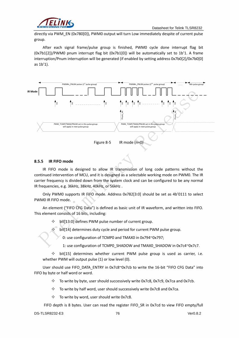
Datasheet for Telink TLSR8232
DS-TLSR8232-E3 76 Ver0.8.2
directly via PWM_EN (0x780[0]), PWM0 output will turn Low immediately despite of current pulse
group.
After each signal frame/pulse group is finished, PWM0 cycle done interrupt flag bit
(0x7b1[2])/PWM0 pnum interrupt flag bit (0x7b1[0]) will be automatically set to 1b’1. A frame
interruption/Pnum interruption will be generated (if enabled by setting address 0x7b0[2]/0x7b0[0]
as 1b’1).
IR Mode
PWM#n_PNUM pulses (1st pulse group) PWM#n_PNUM pulses (2nd pulse group)
Int
Int
Int
Int
Pn
um
_in
t
Int
Int
Int
Int
Int
Int
Pn
um
_in
t
PWM_TCMP/TMAX/PNUM set in this pulse groupwill apply in next pulse group
PWM_TCMP/TMAX/PNUM set in this pulse groupwill apply in next pulse group
…… Nth pulse group
Figure 8-5 IR mode (n=0)
8.5.5 IR FIFO mode
IR FIFO mode is designed to allow IR transmission of long code patterns without the
continued intervention of MCU, and it is designed as a selectable working mode on PWM0. The IR
carrier frequency is divided down from the system clock and can be configured to be any normal
IR frequencies, e.g. 36kHz, 38kHz, 40kHz, or 56kHz .
Only PWM0 supports IR FIFO mode. Address 0x782[3:0] should be set as 4b’0111 to select
PWM0 IR FIFO mode.
An element (“FIFO CFG Data”) is defined as basic unit of IR waveform, and written into FIFO.
This element consists of 16 bits, including:
bit[13:0] defines PWM pulse number of current group.
bit[14] determines duty cycle and period for current PWM pulse group.
0: use configuration of TCMP0 and TMAX0 in 0x794~0x797;
1: use configuration of TCMP0_SHADOW and TMAX0_SHADOW in 0x7c4~0x7c7.
bit[15] determines whether current PWM pulse group is used as carrier, i.e.
whether PWM will output pulse (1) or low level (0).
User should use FIFO_DATA_ENTRY in 0x7c8~0x7cb to write the 16-bit “FIFO CFG Data” into
FIFO by byte or half word or word.
To write by byte, user should successively write 0x7c8, 0x7c9, 0x7ca and 0x7cb.
To write by half word, user should successively write 0x7c8 and 0x7ca.
To write by word, user should write 0x7c8.
FIFO depth is 8 bytes. User can read the register FIFO_SR in 0x7cd to view FIFO empty/full
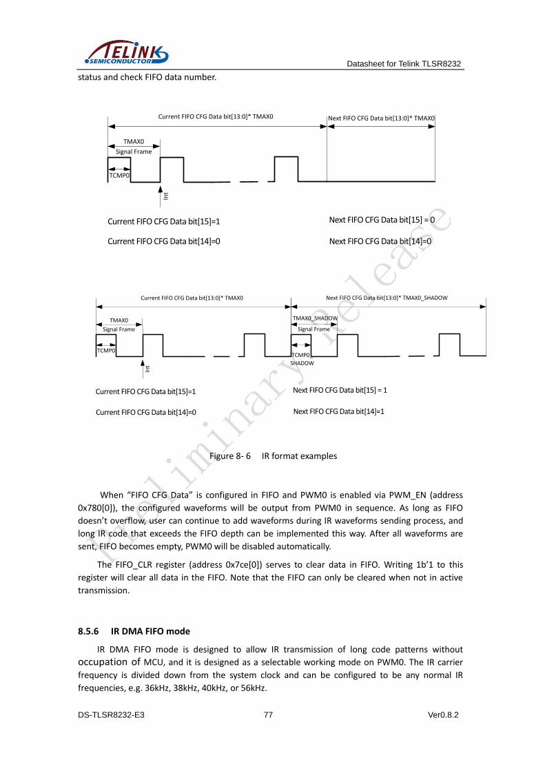
Datasheet for Telink TLSR8232
DS-TLSR8232-E3 77 Ver0.8.2
status and check FIFO data number.
Int
Signal Frame
TCMP0
TMAX0
Current FIFO CFG Data bit[13:0]* TMAX0
Current FIFO CFG Data bit[15]=1 Next FIFO CFG Data bit[15] = 0
Next FIFO CFG Data bit[13:0]* TMAX0
Current FIFO CFG Data bit[14]=0 Next FIFO CFG Data bit[14]=0
Int
Signal Frame
TCMP0
TMAX0
Current FIFO CFG Data bit[13:0]* TMAX0
Current FIFO CFG Data bit[15]=1 Next FIFO CFG Data bit[15] = 1
Signal Frame
TMAX0_SHADOW
Next FIFO CFG Data bit[13:0]* TMAX0_SHADOW
TCMP0_
SHADOW
Current FIFO CFG Data bit[14]=0 Next FIFO CFG Data bit[14]=1
Figure 8- 6 IR format examples
When “FIFO CFG Data” is configured in FIFO and PWM0 is enabled via PWM_EN (address
0x780[0]), the configured waveforms will be output from PWM0 in sequence. As long as FIFO
doesn’t overflow, user can continue to add waveforms during IR waveforms sending process, and
long IR code that exceeds the FIFO depth can be implemented this way. After all waveforms are
sent, FIFO becomes empty, PWM0 will be disabled automatically.
The FIFO_CLR register (address 0x7ce[0]) serves to clear data in FIFO. Writing 1b’1 to this
register will clear all data in the FIFO. Note that the FIFO can only be cleared when not in active
transmission.
8.5.6 IR DMA FIFO mode
IR DMA FIFO mode is designed to allow IR transmission of long code patterns without
occupation of MCU, and it is designed as a selectable working mode on PWM0. The IR carrier
frequency is divided down from the system clock and can be configured to be any normal IR
frequencies, e.g. 36kHz, 38kHz, 40kHz, or 56kHz.
Datasheet for Telink TLSR8232
DS-TLSR8232-E3 78 Ver0.8.2
Only PWM0 supports IR DMA FIFO mode. Address 0x782[3:0] should be set as 4b’1111 to
select PWM0 IR DMA FIFO mode.
This mode is similar to IR FIFO mode, except that “FIFO CFG Data” is written into FIFO by DMA
instead of MCU. User should write the configuration of “FIFO CFG Data” into RAM, and then
enable DMA channel 5. DMA will automatically write the configuration into FIFO.
*Note: In this mode, when DMA channel 5 is enabled, PWM will automatically output configured
waveform, without the need to manually enable PWM0 via 0x780[0] (i.e. 0x780[0] will be set as
1b’1 automatically).
Example 1:
Suppose Mark carrier (pulse) frequency1(F1) = 40kHz, duty cycle 1/3
Mark carrier (pulse) frequency2(F2) = 50kHz, duty cycle 1/2
Space carrier (low level) frequency(F3) = 40kHz
If user wants to make PWM send waveforms in following format (PWM CLK =24MHz):
Burst(20[F1]), i.e. 20 F1 pulses
Burst(30[F2]),
Burst(50[F1]) ,
Burst(50[F2]),
Burst(20[F1],10[F3]),
Burst(30[F2],10[F3])
Step1: Set carrier F1 frequency as 40kHz, set duty cycle as 1/3.
Set PWM_TMAX0 as 0x258 (i.e. 24MHz/40kHz=600=0x258).
Since duty cycle is 1/3, set PWM_TCMP0 as 0xc8 (i.e. 600/3=200=0xc8).
Set carrier F2 frequency as 50kHz, set duty cycle as 1/2.
Set PWM_TMAX0_SHADOW as 0x1e0 (i.e. 24MHz/50kHz=480=0x1e0).
Since duty cycle is 1/2, set PWM_TCMP0_SHADOW as 0xf0 (i.e. 480/2=240=0xf0).
Step2: Generate “FIFO CFG Data” sequence.
Burst(20[F1]): {[15]: 1’b1, [14]: 1’b0, [13:0]: ’d20}=0x8014.
Burst(30[F2]): {[15]: 1’b1, [14]: 1’b1, [13:0]: ’d30}=0xc01e.
Burst(50[F1]) : {[15]: 1’b1, [14]: 1’b0, [13:0]: ’d50}=0x8032.
Burst(50[F2]): {[15]: 1’b1, [14]: 1’b1, [13:0]:’d50}=0xc032.
Burst(20[F1],10[F3]): {[15]: 1’b1, [14]: 1’b0, [13:0]: ’d20}=0x8014,
{[15]: 1’b0, [14]: 1’b0, [13:0]: ’d10}=0x000a.
Datasheet for Telink TLSR8232
DS-TLSR8232-E3 79 Ver0.8.2
Burst(30[F2],10[F3]): {[15]: 1’b1, [14]: 1’b1, [13:0]: ’d30}=0xc01e,
{[15]:1’b0, [14]: 1’b0, [13:0]: ’d10}=0x000a.
Step3: Write “FIFO CFG Data” into SRAM in DMA format.
DMA SOURCE ADDRESS+0x00: 0x0000_0010 (dma transfer-length: 16byte)
DMA SOURCE ADDRESS+0x04: 0xc01e_8014 (LITTLE ENDIAN)
DMA SOURCE ADDRESS+0x08: 0xc032_8032
DMA SOURCE ADDRESS+0x0c: 0x000a_8014
DMA SOURCE ADDRESS+0x10: 0x000a_c01e
Step4: Enable DMA channel 5 to send PWM waveforms.
Write 1’b1 to address 0x524[5] to enable DMA channel 5.
After all waveforms are sent, FIFO becomes empty, PWM0 will be disabled automatically
(address 0x780[0] is automatically cleared). The FIFO mode stop interrupt flag bit (address
0x7b3[0]) will be automatically set as 1b’1. If the interrupt is enabled by setting PWM_MASK1
(address 0x7b2[0]) as 1b’1, a FIFO mode stop interrupt will be generated. User needs to write 1b’1
to the flag bit to manually clear it.
Example 2:
Suppose carrier frequency is 38kHz, system clock frequency is 24MHz, duty cycle is 1/3, and
the format of IR code to be sent is shown as below:
1) Preamble waveform: 9ms carrier + 4.5ms low level.
2) Data 1 waveform: 0.56ms carrier + 0.56ms low level.
3) Data 0 waveform: 0.56ms carrier + 1.69ms low level.
4) Repeat waveform: 9ms carrier + 2.25ms low level + 0.56ms carrier. Repeat
waveform duration is 11.81ms, interval between two adjacent repeat waveforms is
108ms.
5) End waveform: 0.56ms carrier.
User can follow the steps below to configure related registers:
Step1: Set carrier frequency as 38kHz, set duty cycle as 1/3.
Set PWM_TMAX0 as 0x277 (i.e. 24MHz/38kHz=631=0x277).
Since duty cycle is 1/3, set PWM_TCMP0 as 0xd2 (i.e. 631/3=210=0xd2).
Step2: Generate “FIFO CFG Data” sequence.
Preamble waveform:
Datasheet for Telink TLSR8232
DS-TLSR8232-E3 80 Ver0.8.2
9ms carrier: {[15]:1’b1, [14]:1’b0, [13:0]: 9*38=’d 342=14’h 156}=0x8156
4.5ms low level: {[15]:1’b0, [14]:1’b0, [13:0]: 4.5*38=’d 171=14’h ab}=0x00ab
Data 1 waveform:
0.56ms carrier: {[15]:1’b1, [14]:1’b0, [13:0]: 0.56*38=’d 21=14’h 15}=0x8015
0.56ms low level: {[15]:1’b0, [14]:1’b0, [13:0]: 0.56*38=’d 21=14’h 15}=0x0015
Data 0 waveform:
0.56ms carrier: {[15]:1’b1, [14]:1’b0, [13:0]: 0.56*38=’d 21=14’h 15}=0x8015
1.69ms low level: {[15]:1’b0, [14]:1’b0, [13:0]: 1.69*38=’d 64=14’h 40}=0x0040
Repeat waveform:
9ms carrier: {[15]:1’b1, [14]:1’b0, [13:0]: 9*38=’d 342=14’h 156}=0x8156
2.25ms low level: {[15]:1’b0, [14]:1’b0, [13:0]: 2.25*38=’d 86=14’h 56}=0x0056
0.56ms carrier: {[15]:1’b1, [14]:1’b0, [13:0]: 0.56*38=’d 21=14’h 15}=0x8015
108ms -11.81ms =96.19ms low level:
{[15]:1’b0, [14]:1’b0, [13:0]: 96.19*38=’d 3655=14’h e47}=0x0e47
End waveform:
0.56ms carrier: {[15]:1’b1, [14]:1’b0, [13:0]: 0.56*38=’d 21=14’h 15}=0x8015
Step3: Write “IR CFG Data” into SRAM in DMA format.
If user want PWM0 to send IR waveform in following format:
Preamble+0x5a+Repeat+End
Preamble: 0x8156, 0x00ab
0x5a=8’b01011010
Data 0: 0x8015, 0x0040
Data 1: 0x8015, 0x0015
Data 0: 0x8015, 0x0040
Data 1: 0x8015, 0x0015
Data 1: 0x8015, 0x0015
Data 0: 0x8015, 0x0040
Data 1: 0x8015, 0x0015
Data 0: 0x8015, 0x0040
Repeat: 0x8156, 0x0056, 0x8015, 0x0e47
End: 0x8015.
User needs to write the configuration information above into source address of DMA channel
5, as shown below:
DMA SOURCE ADDRESS+0x00: 0x0000_002e (dma transfer-length: 46byte)
Datasheet for Telink TLSR8232
DS-TLSR8232-E3 81 Ver0.8.2
DMA SOURCE ADDRESS+0x04: 0x00ab_8156 (Preamble) (LITTLE ENDIAN)
DMA SOURCE ADDRESS+0x08: 0x0040_8015 (Data 0)
DMA SOURCE ADDRESS+0x0c: 0x0015_8015 (Data 1)
DMA SOURCE ADDRESS+0x10: 0x0040_8015 (Data 0)
DMA SOURCE ADDRESS+0x14: 0x0015_8015 (Data 1)
DMA SOURCE ADDRESS+0x18: 0x0015_8015 (Data 1)
DMA SOURCE ADDRESS+0x1c: 0x0040_8015 (Data 0)
DMA SOURCE ADDRESS+0x20: 0x0015_8015 (Data 1)
DMA SOURCE ADDRESS+0x24: 0x0040_8015 (Data 0)
DMA SOURCE ADDRESS+0x28: 0x0056_8156 (Repeat)
DMA SOURCE ADDRESS+0x2c: 0x0e47_8015 (Repeat)
DMA SOURCE ADDRESS+0x30: 0x8015 (End)
Step4: Enable DMA channel 5 to send PWM waveforms.
Write 1’b1 to address 0x524[5] to enable DMA channel 5.
After all waveforms are sent, FIFO becomes empty, PWM0 will be disabled automatically
(address 0x780[0] is automatically cleared). The FIFO mode stop interrupt flag bit (address
0x7b3[0]) will be automatically set as 1b’1. If the interrupt is enabled by setting PWM_MASK1
(address 0x7b2[0]) as 1b’1, a FIFO mode stop interrupt will be generated. User needs to write 1b’1
to the flag bit to manually clear it.
8.6 PWM interrupt
There are 9 interrupt sources from PWM function.
After each signal frame, PWM#n (n=0~5) will generate a frame-done IRQ (Interrupt Request)
signal.
In Counting mode and IR mode, PWM0 will generate a Pnum IRQ signal after completing a
pulse group.
In IR FIFO mode, PWM0 will generate a FIFO mode count IRQ signal when the FIFO_NUM
value is less than the FIFO_NUM_LVL, and will generate a FIFO mode stop IRQ signal after FIFO
becomes empty.
In IR DMA FIFO mode, PWM0 will generate an IR waveform send done IRQ signal, after DMA
has sent all configuration data, FIFO becomes empty and final waveform is sent.
To enable PWM interrupt, the total enabling bit “irq_pwm” (address 0x641[6], see section 6
Interrupt) should be set as 1b’1. To enable various PWM interrupt sources, PWM_MASK0 (address
0x7b0[7:0]) and PWM_MASK1 (address 0x7b2[0]) should be set as 1b’1 correspondingly.
Interrupt status can be cleared via register PWM_INT0 (address 0x7b1[7:0]) and PWM_INT1
(address 0x7b3[0]).
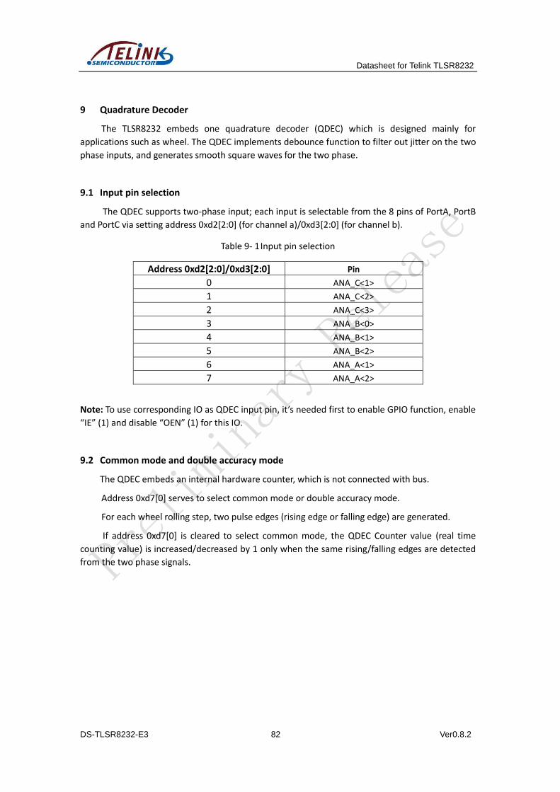
Datasheet for Telink TLSR8232
DS-TLSR8232-E3 82 Ver0.8.2
9 Quadrature Decoder
The TLSR8232 embeds one quadrature decoder (QDEC) which is designed mainly for
applications such as wheel. The QDEC implements debounce function to filter out jitter on the two
phase inputs, and generates smooth square waves for the two phase.
9.1 Input pin selection
The QDEC supports two-phase input; each input is selectable from the 8 pins of PortA, PortB
and PortC via setting address 0xd2[2:0] (for channel a)/0xd3[2:0] (for channel b).
Table 9- 1 Input pin selection
Address 0xd2[2:0]/0xd3[2:0] Pin
0 ANA_C<1>
1 ANA_C<2>
2 ANA_C<3>
3 ANA_B<0>
4 ANA_B<1>
5 ANA_B<2>
6 ANA_A<1>
7 ANA_A<2>
Note: To use corresponding IO as QDEC input pin, it’s needed first to enable GPIO function, enable
“IE” (1) and disable “OEN” (1) for this IO.
9.2 Common mode and double accuracy mode
The QDEC embeds an internal hardware counter, which is not connected with bus.
Address 0xd7[0] serves to select common mode or double accuracy mode.
For each wheel rolling step, two pulse edges (rising edge or falling edge) are generated.
If address 0xd7[0] is cleared to select common mode, the QDEC Counter value (real time
counting value) is increased/decreased by 1 only when the same rising/falling edges are detected
from the two phase signals.
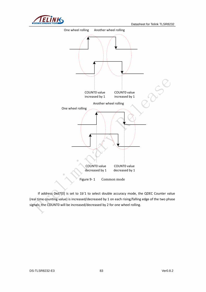
Datasheet for Telink TLSR8232
DS-TLSR8232-E3 83 Ver0.8.2
One wheel rolling
COUNT0 value increased by 1
Another wheel rolling
COUNT0 value increased by 1
One wheel rolling
COUNT0 value decreased by 1
Another wheel rolling
COUNT0 value decreased by 1
Figure 9- 1 Common mode
If address 0xd7[0] is set to 1b’1 to select double accuracy mode, the QDEC Counter value
(real time counting value) is increased/decreased by 1 on each rising/falling edge of the two phase
signals; the COUNT0 will be increased/decreased by 2 for one wheel rolling.
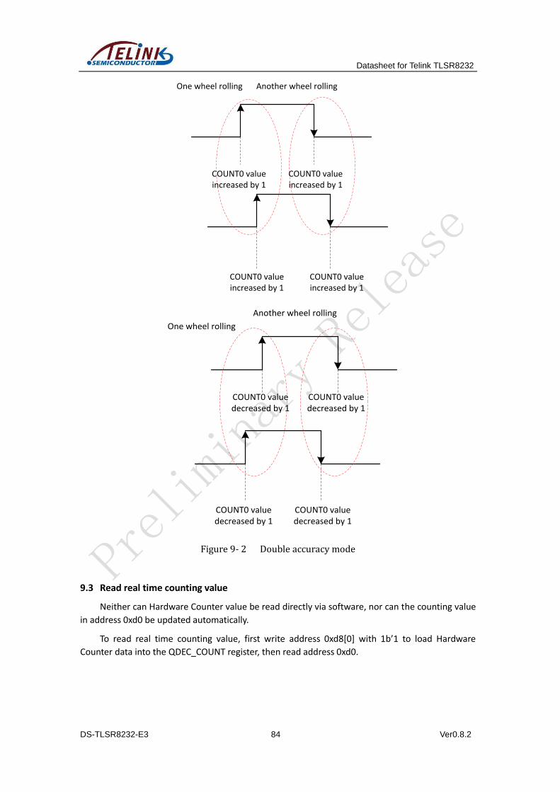
Datasheet for Telink TLSR8232
DS-TLSR8232-E3 84 Ver0.8.2
One wheel rolling
COUNT0 value increased by 1
Another wheel rolling
COUNT0 value increased by 1
COUNT0 value increased by 1
COUNT0 value increased by 1
One wheel rolling
COUNT0 value decreased by 1
Another wheel rolling
COUNT0 value decreased by 1
COUNT0 value decreased by 1
COUNT0 value decreased by 1
Figure 9- 2 Double accuracy mode
9.3 Read real time counting value
Neither can Hardware Counter value be read directly via software, nor can the counting value
in address 0xd0 be updated automatically.
To read real time counting value, first write address 0xd8[0] with 1b’1 to load Hardware
Counter data into the QDEC_COUNT register, then read address 0xd0.
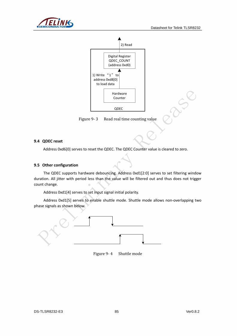
Datasheet for Telink TLSR8232
DS-TLSR8232-E3 85 Ver0.8.2
Hardware Counter
Digital Register QDEC_COUNT(address 0xd0)
1) Write “1” to address 0xd8[0]
to load data
QDEC
2) Read
Figure 9- 3 Read real time counting value
9.4 QDEC reset
Address 0xd6[0] serves to reset the QDEC. The QDEC Counter value is cleared to zero.
9.5 Other configuration
The QDEC supports hardware debouncing. Address 0xd1[2:0] serves to set filtering window
duration. All jitter with period less than the value will be filtered out and thus does not trigger
count change.
Address 0xd1[4] serves to set input signal initial polarity.
Address 0xd1[5] serves to enable shuttle mode. Shuttle mode allows non-overlapping two
phase signals as shown below.
Figure 9- 4 Shuttle mode
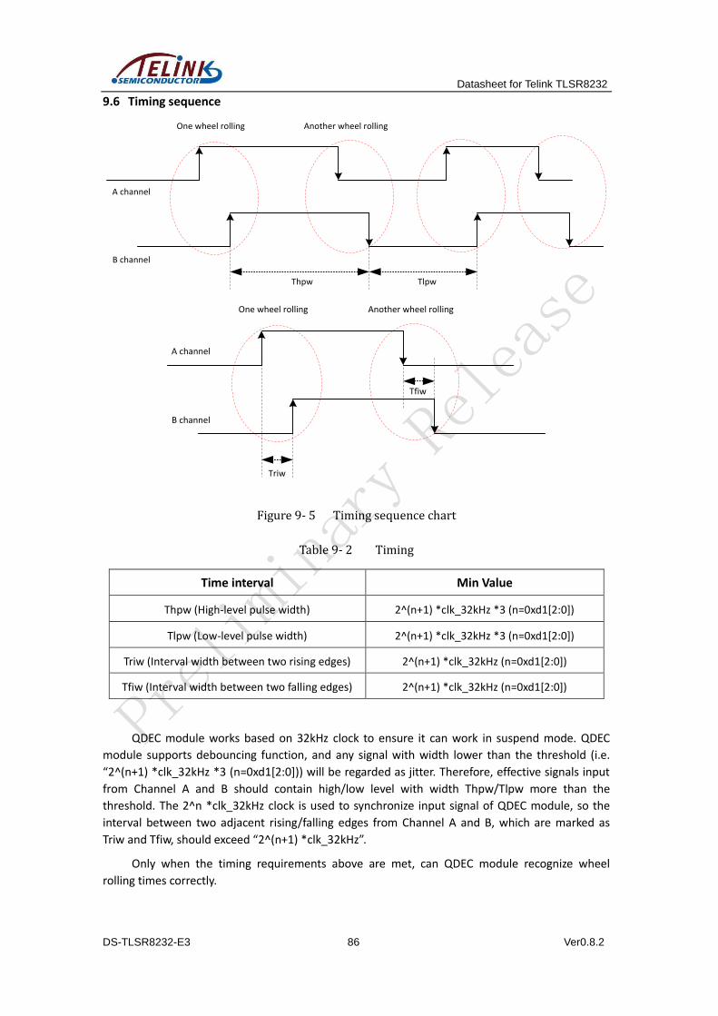
Datasheet for Telink TLSR8232
DS-TLSR8232-E3 86 Ver0.8.2
9.6 Timing sequence
One wheel rolling Another wheel rolling
Thpw Tlpw
A channel
B channel
One wheel rolling Another wheel rolling
Triw
Tfiw
A channel
B channel
Figure 9- 5 Timing sequence chart
Table 9- 2 Timing
Time interval Min Value
Thpw (High-level pulse width) 2^(n+1) *clk_32kHz *3 (n=0xd1[2:0])
Tlpw (Low-level pulse width) 2^(n+1) *clk_32kHz *3 (n=0xd1[2:0])
Triw (Interval width between two rising edges) 2^(n+1) *clk_32kHz (n=0xd1[2:0])
Tfiw (Interval width between two falling edges) 2^(n+1) *clk_32kHz (n=0xd1[2:0])
QDEC module works based on 32kHz clock to ensure it can work in suspend mode. QDEC
module supports debouncing function, and any signal with width lower than the threshold (i.e.
“2^(n+1) *clk_32kHz *3 (n=0xd1[2:0])) will be regarded as jitter. Therefore, effective signals input
from Channel A and B should contain high/low level with width Thpw/Tlpw more than the
threshold. The 2^n *clk_32kHz clock is used to synchronize input signal of QDEC module, so the
interval between two adjacent rising/falling edges from Channel A and B, which are marked as
Triw and Tfiw, should exceed “2^(n+1) *clk_32kHz”.
Only when the timing requirements above are met, can QDEC module recognize wheel
rolling times correctly.
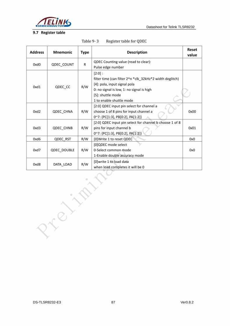
Datasheet for Telink TLSR8232
DS-TLSR8232-E3 87 Ver0.8.2
9.7 Register table
Table 9- 3 Register table for QDEC
Address Mnemonic Type Description Reset
value
0xd0 QDEC_COUNT R QDEC Counting value (read to clear):
Pulse edge number
0xd1 QDEC_CC R/W
[2:0] :
filter time (can filter 2^n *clk_32kHz*2 width deglitch)
[4]: pola, input signal pola
0: no signal is low, 1: no signal is high
[5]: shuttle mode
1 to enable shuttle mode
0xd2 QDEC_CHNA R/W
[2:0] QDEC input pin select for channel a
choose 1 of 8 pins for input channel a
0~7: {PC[1:3], PB[0:2], PA[1:2]}
0x00
0xd3 QDEC_CHNB R/W
[2:0] QDEC input pin select for channel b choose 1 of 8
pins for input channel b
0~7: {PC[1:3], PB[0:2], PA[1:2]}
0x01
0xd6 QDEC_RST R/W [0]Write 1 to reset QDEC 0x0
0xd7 QDEC_DOUBLE R/W
[0]QDEC mode select
0-Select common mode
1-Enable double accuracy mode
0x0
0xd8 DATA_LOAD R/W [0]write 1 to load data
when load completes it will be 0
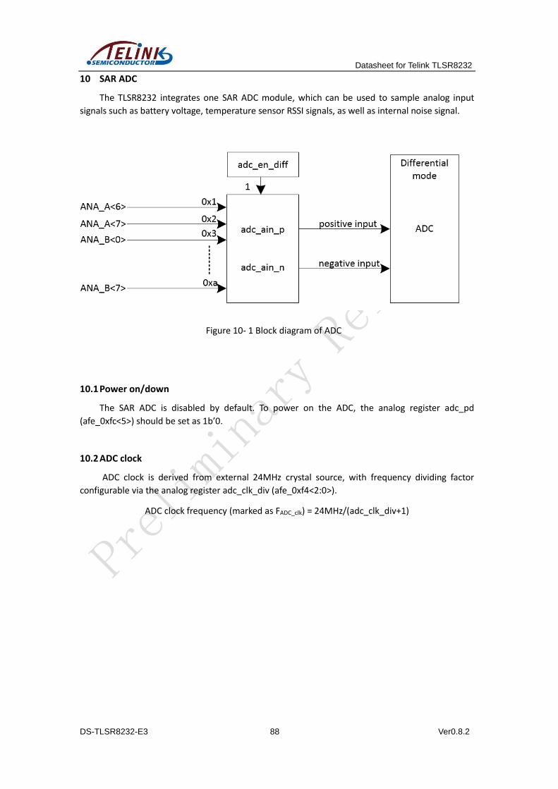
Datasheet for Telink TLSR8232
DS-TLSR8232-E3 88 Ver0.8.2
10 SAR ADC
The TLSR8232 integrates one SAR ADC module, which can be used to sample analog input
signals such as battery voltage, temperature sensor RSSI signals, as well as internal noise signal.
Figure 10- 1 Block diagram of ADC
10.1 Power on/down
The SAR ADC is disabled by default. To power on the ADC, the analog register adc_pd
(afe_0xfc<5>) should be set as 1b’0.
10.2 ADC clock
ADC clock is derived from external 24MHz crystal source, with frequency dividing factor
configurable via the analog register adc_clk_div (afe_0xf4<2:0>).
ADC clock frequency (marked as FADC_clk) = 24MHz/(adc_clk_div+1)
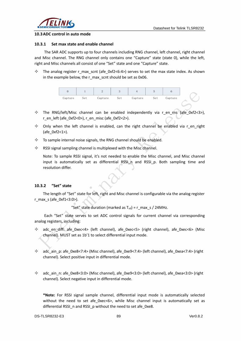
Datasheet for Telink TLSR8232
DS-TLSR8232-E3 89 Ver0.8.2
10.3 ADC control in auto mode
10.3.1 Set max state and enable channel
The SAR ADC supports up to four channels including RNG channel, left channel, right channel
and Misc channel. The RNG channel only contains one “Capture” state (state 0), while the left,
right and Misc channels all consist of one “Set” state and one “Capture” state.
The analog register r_max_scnt (afe_0xf2<6:4>) serves to set the max state index. As shown
in the example below, the r_max_scnt should be set as 0x06.
0 1 2 3 4 5 6
Set Set SetCapture Capture CaptureCapture
The RNG/left/Misc channel can be enabled independently via r_en_rns (afe_0xf2<3>),
r_en_left (afe_0xf2<0>), r_en_misc (afe_0xf2<2>).
Only when the left channel is enabled, can the right channel be enabled via r_en_right
(afe_0xf2<1>).
To sample internal noise signals, the RNG channel should be enabled.
RSSI signal sampling channel is multiplexed with the Misc channel.
Note: To sample RSSI signal, it’s not needed to enable the Misc channel, and Misc channel
input is automatically set as differential RSSI_n and RSSI_p. Both sampling time and
resolution differ.
10.3.2 “Set” state
The length of “Set” state for left, right and Misc channel is configurable via the analog register
r_max_s (afe_0xf1<3:0>).
“Set” state duration (marked as Tsd) = r_max_s / 24MHz.
Each “Set” state serves to set ADC control signals for current channel via corresponding
analog registers, including:
adc_en_diff: afe_0xec<4> (left channel), afe_0xec<5> (right channel), afe_0xec<6> (Misc
channel). MUST set as 1b’1 to select differential input mode.
adc_ain_p: afe_0xe8<7:4> (Misc channel), afe_0xe9<7:4> (left channel), afe_0xea<7:4> (right
channel). Select positive input in differential mode.
adc_ain_n: afe_0xe8<3:0> (Misc channel), afe_0xe9<3:0> (left channel), afe_0xea<3:0> (right
channel). Select negative input in differential mode.
*Note: For RSSI signal sample channel, differential input mode is automatically selected
without the need to set afe_0xec<6>, while Misc channel input is automatically set as
differential RSSI_n and RSSI_p without the need to set afe_0xe8.

Datasheet for Telink TLSR8232
DS-TLSR8232-E3 90 Ver0.8.2
adc_vref: afe_0xe7<1:0> (left channel), afe_0xe7<3:2> (right channel), afe_0xe7<5:4> (Misc
channel). Set reference voltage VREF. ADC maximum input range is the determined by the ADC
reference voltage.
adc_sel_ai_scale: afe_0xfa<7:6>. Set scaling factor for ADC analog input as 1 (default), 1/2,
1/4 or 1/8.
By setting this scaling factor, ADC maximum input range can be extended based on the VREF.
For example, suppose the VREF is set as 1.2V:
Since the scaling factor is 1 by default, the ADC maximum input range should be -1.2V~+1.2V
(differential mode).
If the scaling factor is set as 1/2, ADC maximum input range should change to -2.4V~+2.4V
(differential mode).
adc_res: afe_0xeb<1:0> (left channel), afe_0xeb<5:4> (right channel), afe_0xec<1:0> (Misc
channel). Set resolution as 8/10/12/14 bits.
*Note: For RSSI signal sample channel, resolution is fixed as 8bits without the need to set
afe_0xec<1:0>.
ADC data is always 15-bit format no matter how the resolution is set. For example, 14 bits
resolution indicates ADC data consists of 14-bit valid data and 1-bit sign extension bit.
adc_tsamp: afe_0xed<3:0> (left channel), afe_0xed<7:4> (right channel), afe_0xee<3:0> (Misc
channel), afe_0xee<7:4> (RSSI signal sample channel). Set sampling time which determines
the speed to stabilize input signals.
Sampling time (marked as Tsamp) = adc_tsamp / FADC_clk.
The lower sampling cycle, the shorter ADC convert time.
pga_boost, pga_gain: Set PGA gain in Boost stage and Gain stage. See PGA section.
10.3.3 “Capture” state
For the RNG channel, the “Capture” state serves to capture random number sequence (RNS)
derived from internal noise.
For the left, right and Misc channels, at the beginning of each “Capture” state, run signal is
issued automatically to start an ADC sampling and conversion process; at the end of each “Capture”
state, ADC output data is captured.
The length of “Capture” state for RNS and Misc channel is configurable via the analog register
r_max_mc[9:0] (afe_0xf1<7:6>, afe_0xef<7:0>).
“Capture” state duration for RNS & Misc channel (marked as Tcd) = r_max_mc / 24MHz.
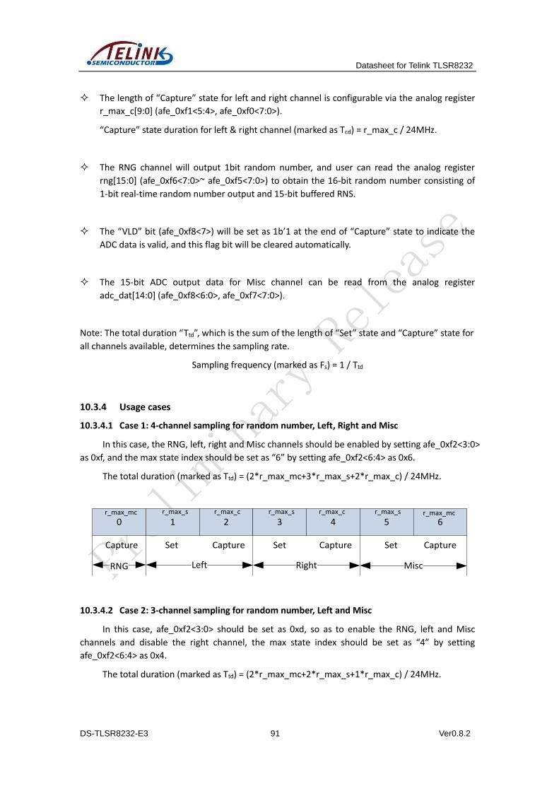
Datasheet for Telink TLSR8232
DS-TLSR8232-E3 91 Ver0.8.2
The length of “Capture” state for left and right channel is configurable via the analog register
r_max_c[9:0] (afe_0xf1<5:4>, afe_0xf0<7:0>).
“Capture” state duration for left & right channel (marked as Tcd) = r_max_c / 24MHz.
The RNG channel will output 1bit random number, and user can read the analog register
rng[15:0] (afe_0xf6<7:0>~ afe_0xf5<7:0>) to obtain the 16-bit random number consisting of
1-bit real-time random number output and 15-bit buffered RNS.
The “VLD” bit (afe_0xf8<7>) will be set as 1b’1 at the end of “Capture” state to indicate the
ADC data is valid, and this flag bit will be cleared automatically.
The 15-bit ADC output data for Misc channel can be read from the analog register
adc_dat[14:0] (afe_0xf8<6:0>, afe_0xf7<7:0>).
Note: The total duration “Ttd”, which is the sum of the length of “Set” state and “Capture” state for
all channels available, determines the sampling rate.
Sampling frequency (marked as Fs) = 1 / Ttd
10.3.4 Usage cases
10.3.4.1 Case 1: 4-channel sampling for random number, Left, Right and Misc
In this case, the RNG, left, right and Misc channels should be enabled by setting afe_0xf2<3:0>
as 0xf, and the max state index should be set as “6” by setting afe_0xf2<6:4> as 0x6.
The total duration (marked as Ttd) = (2*r_max_mc+3*r_max_s+2*r_max_c) / 24MHz.
0 1 2 3 4 5 6
Set Set SetCapture Capture CaptureCapture
RNG Left Right Misc
r_max_mc r_max_mcr_max_s r_max_s r_max_sr_max_c r_max_c
10.3.4.2 Case 2: 3-channel sampling for random number, Left and Misc
In this case, afe_0xf2<3:0> should be set as 0xd, so as to enable the RNG, left and Misc
channels and disable the right channel, the max state index should be set as “4” by setting
afe_0xf2<6:4> as 0x4.
The total duration (marked as Ttd) = (2*r_max_mc+2*r_max_s+1*r_max_c) / 24MHz.
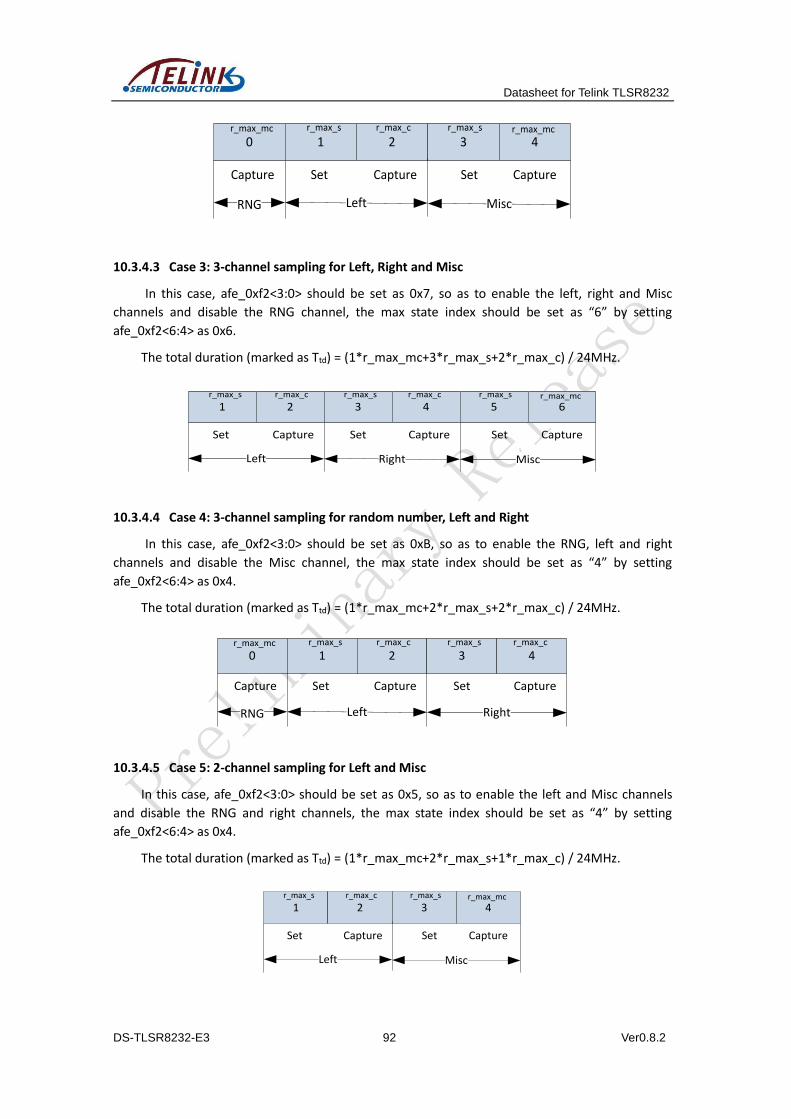
Datasheet for Telink TLSR8232
DS-TLSR8232-E3 92 Ver0.8.2
0 1 2 3 4
Set SetCapture CaptureCapture
RNG Left Misc
r_max_mc r_max_mcr_max_s r_max_sr_max_c
10.3.4.3 Case 3: 3-channel sampling for Left, Right and Misc
In this case, afe_0xf2<3:0> should be set as 0x7, so as to enable the left, right and Misc
channels and disable the RNG channel, the max state index should be set as “6” by setting
afe_0xf2<6:4> as 0x6.
The total duration (marked as Ttd) = (1*r_max_mc+3*r_max_s+2*r_max_c) / 24MHz.
1 2 3 4 5 6
Set Set SetCapture Capture Capture
Left Right Misc
r_max_mcr_max_s r_max_s r_max_sr_max_c r_max_c
10.3.4.4 Case 4: 3-channel sampling for random number, Left and Right
In this case, afe_0xf2<3:0> should be set as 0xB, so as to enable the RNG, left and right
channels and disable the Misc channel, the max state index should be set as “4” by setting
afe_0xf2<6:4> as 0x4.
The total duration (marked as Ttd) = (1*r_max_mc+2*r_max_s+2*r_max_c) / 24MHz.
0 1 2 3 4
Set SetCapture CaptureCapture
RNG Left Right
r_max_mc r_max_s r_max_sr_max_c r_max_c
10.3.4.5 Case 5: 2-channel sampling for Left and Misc
In this case, afe_0xf2<3:0> should be set as 0x5, so as to enable the left and Misc channels
and disable the RNG and right channels, the max state index should be set as “4” by setting
afe_0xf2<6:4> as 0x4.
The total duration (marked as Ttd) = (1*r_max_mc+2*r_max_s+1*r_max_c) / 24MHz.
1 2 3 4
Set SetCapture Capture
Left Misc
r_max_mcr_max_s r_max_sr_max_c
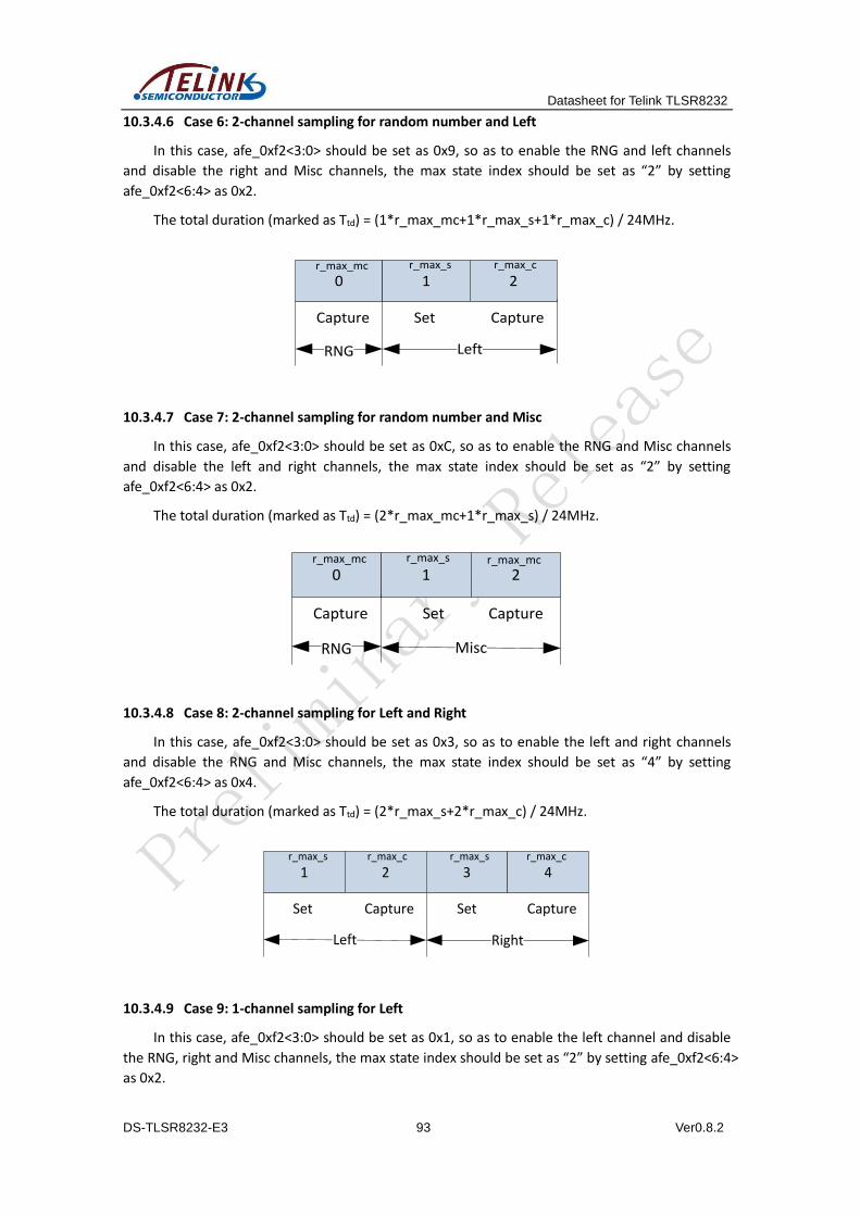
Datasheet for Telink TLSR8232
DS-TLSR8232-E3 93 Ver0.8.2
10.3.4.6 Case 6: 2-channel sampling for random number and Left
In this case, afe_0xf2<3:0> should be set as 0x9, so as to enable the RNG and left channels
and disable the right and Misc channels, the max state index should be set as “2” by setting
afe_0xf2<6:4> as 0x2.
The total duration (marked as Ttd) = (1*r_max_mc+1*r_max_s+1*r_max_c) / 24MHz.
0 1 2
Set CaptureCapture
RNG Left
r_max_mc r_max_s r_max_c
10.3.4.7 Case 7: 2-channel sampling for random number and Misc
In this case, afe_0xf2<3:0> should be set as 0xC, so as to enable the RNG and Misc channels
and disable the left and right channels, the max state index should be set as “2” by setting
afe_0xf2<6:4> as 0x2.
The total duration (marked as Ttd) = (2*r_max_mc+1*r_max_s) / 24MHz.
0 1 2
Set CaptureCapture
RNG Misc
r_max_mc r_max_mcr_max_s
10.3.4.8 Case 8: 2-channel sampling for Left and Right
In this case, afe_0xf2<3:0> should be set as 0x3, so as to enable the left and right channels
and disable the RNG and Misc channels, the max state index should be set as “4” by setting
afe_0xf2<6:4> as 0x4.
The total duration (marked as Ttd) = (2*r_max_s+2*r_max_c) / 24MHz.
1 2 3 4
Set SetCapture Capture
Left Right
r_max_s r_max_sr_max_c r_max_c
10.3.4.9 Case 9: 1-channel sampling for Left
In this case, afe_0xf2<3:0> should be set as 0x1, so as to enable the left channel and disable
the RNG, right and Misc channels, the max state index should be set as “2” by setting afe_0xf2<6:4>
as 0x2.
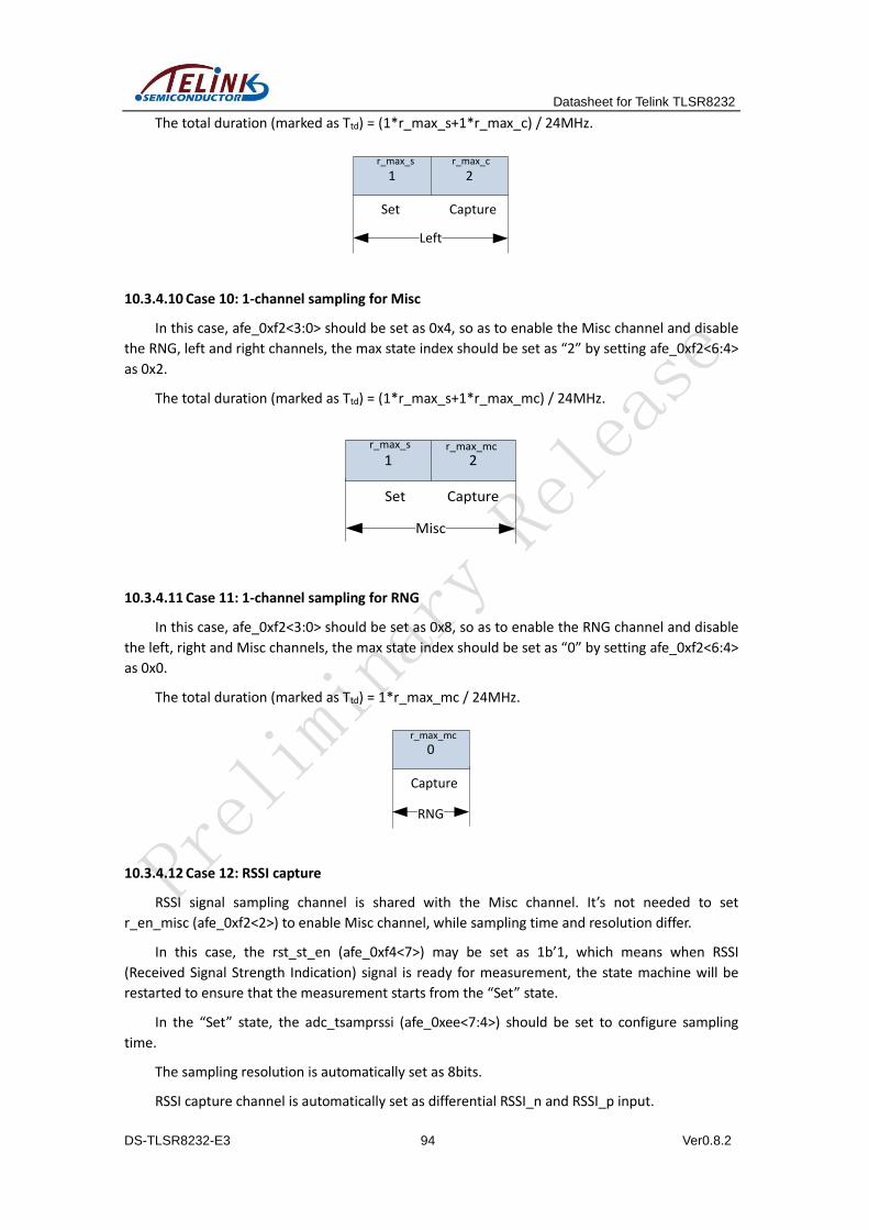
Datasheet for Telink TLSR8232
DS-TLSR8232-E3 94 Ver0.8.2
The total duration (marked as Ttd) = (1*r_max_s+1*r_max_c) / 24MHz.
1 2
Set Capture
Left
r_max_s r_max_c
10.3.4.10 Case 10: 1-channel sampling for Misc
In this case, afe_0xf2<3:0> should be set as 0x4, so as to enable the Misc channel and disable
the RNG, left and right channels, the max state index should be set as “2” by setting afe_0xf2<6:4>
as 0x2.
The total duration (marked as Ttd) = (1*r_max_s+1*r_max_mc) / 24MHz.
1 2
Set Capture
Misc
r_max_mcr_max_s
10.3.4.11 Case 11: 1-channel sampling for RNG
In this case, afe_0xf2<3:0> should be set as 0x8, so as to enable the RNG channel and disable
the left, right and Misc channels, the max state index should be set as “0” by setting afe_0xf2<6:4>
as 0x0.
The total duration (marked as Ttd) = 1*r_max_mc / 24MHz.
0
Capture
RNG
r_max_mc
10.3.4.12 Case 12: RSSI capture
RSSI signal sampling channel is shared with the Misc channel. It’s not needed to set
r_en_misc (afe_0xf2<2>) to enable Misc channel, while sampling time and resolution differ.
In this case, the rst_st_en (afe_0xf4<7>) may be set as 1b’1, which means when RSSI
(Received Signal Strength Indication) signal is ready for measurement, the state machine will be
restarted to ensure that the measurement starts from the “Set” state.
In the “Set” state, the adc_tsamprssi (afe_0xee<7:4>) should be set to configure sampling
time.
The sampling resolution is automatically set as 8bits.
RSSI capture channel is automatically set as differential RSSI_n and RSSI_p input.
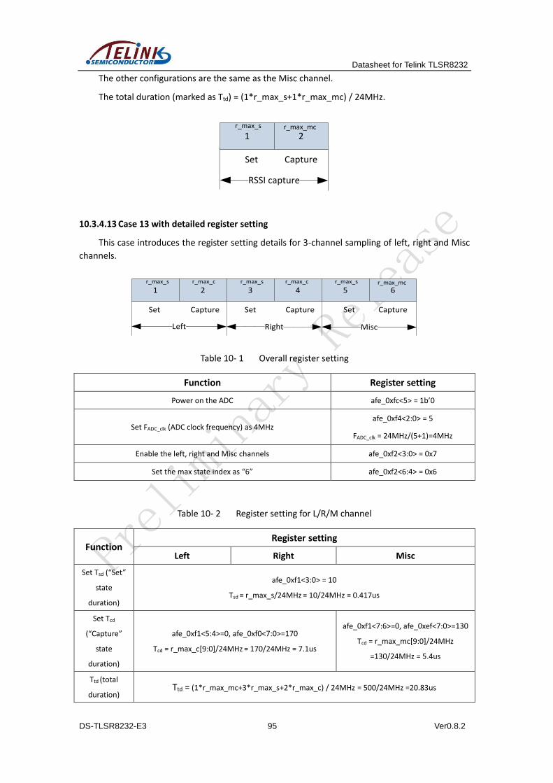
Datasheet for Telink TLSR8232
DS-TLSR8232-E3 95 Ver0.8.2
The other configurations are the same as the Misc channel.
The total duration (marked as Ttd) = (1*r_max_s+1*r_max_mc) / 24MHz.
1 2
Set Capture
RSSI capture
r_max_mcr_max_s
10.3.4.13 Case 13 with detailed register setting
This case introduces the register setting details for 3-channel sampling of left, right and Misc
channels.
1 2 3 4 5 6
Set Set SetCapture Capture Capture
Left Right Misc
r_max_mcr_max_s r_max_s r_max_sr_max_c r_max_c
Table 10- 1 Overall register setting
Function Register setting
Power on the ADC afe_0xfc<5> = 1b’0
Set FADC_clk (ADC clock frequency) as 4MHz afe_0xf4<2:0> = 5
FADC_clk = 24MHz/(5+1)=4MHz
Enable the left, right and Misc channels afe_0xf2<3:0> = 0x7
Set the max state index as “6” afe_0xf2<6:4> = 0x6
Table 10- 2 Register setting for L/R/M channel
Function Register setting
Left Right Misc
Set Tsd (“Set”
state
duration)
afe_0xf1<3:0> = 10
Tsd = r_max_s/24MHz = 10/24MHz = 0.417us
Set Tcd
(“Capture”
state
duration)
afe_0xf1<5:4>=0, afe_0xf0<7:0>=170
Tcd = r_max_c[9:0]/24MHz = 170/24MHz = 7.1us
afe_0xf1<7:6>=0, afe_0xef<7:0>=130
Tcd = r_max_mc[9:0]/24MHz
=130/24MHz = 5.4us
Ttd (total
duration) Ttd = (1*r_max_mc+3*r_max_s+2*r_max_c) / 24MHz = 500/24MHz =20.83us
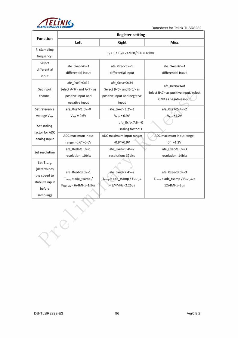
Datasheet for Telink TLSR8232
DS-TLSR8232-E3 96 Ver0.8.2
Function Register setting
Left Right Misc
Fs (Sampling
frequency) Fs = 1 / Ttd = 24MHz/500 = 48kHz
Select
differential
input
afe_0xec<4>=1
differential input
afe_0xec<5>=1
differential input
afe_0xec<6>=1
differential input
Set input
channel
afe_0xe9=0x12
Select A<6> and A<7> as
positive input and
negative input
afe_0xea=0x34
Select B<0> and B<1> as
positive input and negative
input
afe_0xe8=0xaf
Select B<7> as positive input, select
GND as negative input
Set reference
voltage VREF
afe_0xe7<1:0>=0
VREF = 0.6V
afe_0xe7<3:2>=1
VREF = 0.9V
afe_0xe7<5:4>=2
VREF =1.2V
Set scaling
factor for ADC
analog input
afe_0xfa<7:6>=0
scaling factor: 1
ADC maximum input
range: -0.6~+0.6V
ADC maximum input range:
-0.9~+0.9V
ADC maximum input range:
0 ~ +1.2V
Set resolution afe_0xeb<1:0>=1
resolution: 10bits
afe_0xeb<5:4>=2
resolution: 12bits
afe_0xec<1:0>=3
resolution: 14bits
Set Tsamp
(determines
the speed to
stabilize input
before
sampling)
afe_0xed<3:0>=1
Tsamp = adc_tsamp /
FADC_clk = 6/4MHz=1.5us
afe_0xed<7:4>=2
Tsamp = adc_tsamp / FADC_clk
= 9/4MHz=2.25us
afe_0xee<3:0>=3
Tsamp = adc_tsamp / FADC_clk =
12/4MHz=3us
Datasheet for Telink TLSR8232
DS-TLSR8232-E3 97 Ver0.8.2
10.4 Register table
Table 10- 3 Register table related to SAR ADC
Address Mnemonic Default
value Description
afe_0xe7<1:0> adc_vrefl 00
Select VREF for left channel
0x0: 0.6V
0x1: 0.9V
0x2: 1.2V
0x3: VBAT/N (N=2/3/4, when
afe_1P2V_reg121<3:2> is set as 0x3/0x2/0x1).
afe_0xe7<3:2> adc_vrefr 00
Select VREF for right channel
0x0: 0.6V
0x1: 0.9V
0x2: 1.2V
0x3: VBAT/N (N=2/3/4, when
afe_1P2V_reg121<3:2> is set as 0x3/0x2/0x1)
afe_0xe7<5:4> adc_vrefm 00
Select VREF for Misc channel
0x0: 0.6V
0x1: 0.9V
0x2: 1.2V
0x3: VBAT/N (N=2/3/4, when afe_0xf9<3:2> is set
as 0x3/0x2/0x1)
afe_0xe7<7:6> RSVD
afe_0xe8<3:0> adc_ain_m_n 0000
Select negative input for Misc channel:
0x0: No input
0x1: A<6>
0x2: A<7>
0x3: B<0>
0x4: B<1>
……
0xa: B<7>
0xb: pga_channel_n<0> (PGA negative output)
0xc: rsvd
0xd: rsvd
0xe: tempsensor_n (temperature sensor negative
output)
0xf: Ground
afe_0xe8<7:4> adc_ain_m_p 0000
Select positive input for Misc channel:
(For RNS mode, must set as 0x0.)
0x0: No input
0x1: A<6>
0x2: A<7>
0x3: B<0>
0x4: B<1>
……
0xa: B<7>
0xb: pga_channel_p<0> (PGA positive output)
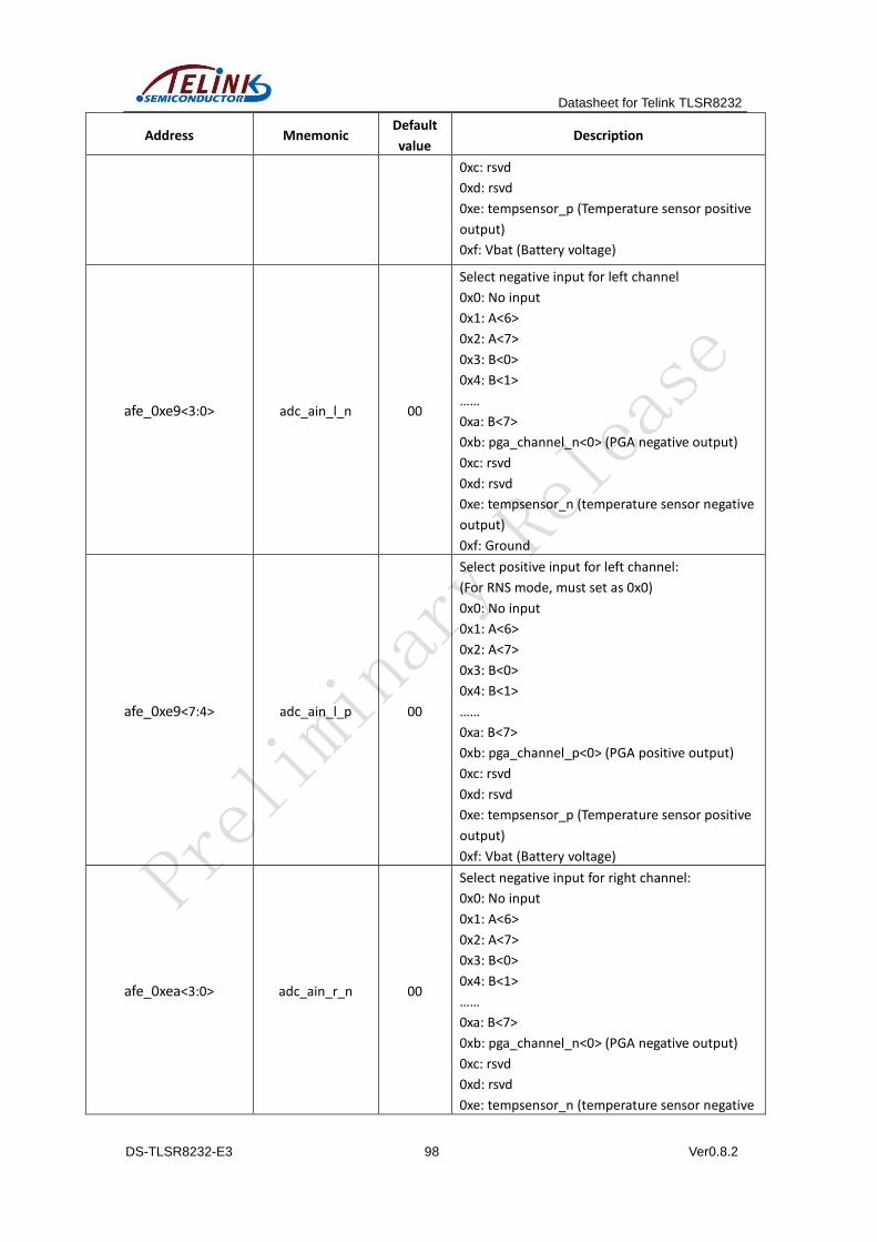
Datasheet for Telink TLSR8232
DS-TLSR8232-E3 98 Ver0.8.2
Address Mnemonic Default
value Description
0xc: rsvd
0xd: rsvd
0xe: tempsensor_p (Temperature sensor positive
output)
0xf: Vbat (Battery voltage)
afe_0xe9<3:0> adc_ain_l_n 00
Select negative input for left channel
0x0: No input
0x1: A<6>
0x2: A<7>
0x3: B<0>
0x4: B<1>
……
0xa: B<7>
0xb: pga_channel_n<0> (PGA negative output)
0xc: rsvd
0xd: rsvd
0xe: tempsensor_n (temperature sensor negative
output)
0xf: Ground
afe_0xe9<7:4> adc_ain_l_p 00
Select positive input for left channel:
(For RNS mode, must set as 0x0)
0x0: No input
0x1: A<6>
0x2: A<7>
0x3: B<0>
0x4: B<1>
……
0xa: B<7>
0xb: pga_channel_p<0> (PGA positive output)
0xc: rsvd
0xd: rsvd
0xe: tempsensor_p (Temperature sensor positive
output)
0xf: Vbat (Battery voltage)
afe_0xea<3:0> adc_ain_r_n 00
Select negative input for right channel:
0x0: No input
0x1: A<6>
0x2: A<7>
0x3: B<0>
0x4: B<1>
……
0xa: B<7>
0xb: pga_channel_n<0> (PGA negative output)
0xc: rsvd
0xd: rsvd
0xe: tempsensor_n (temperature sensor negative
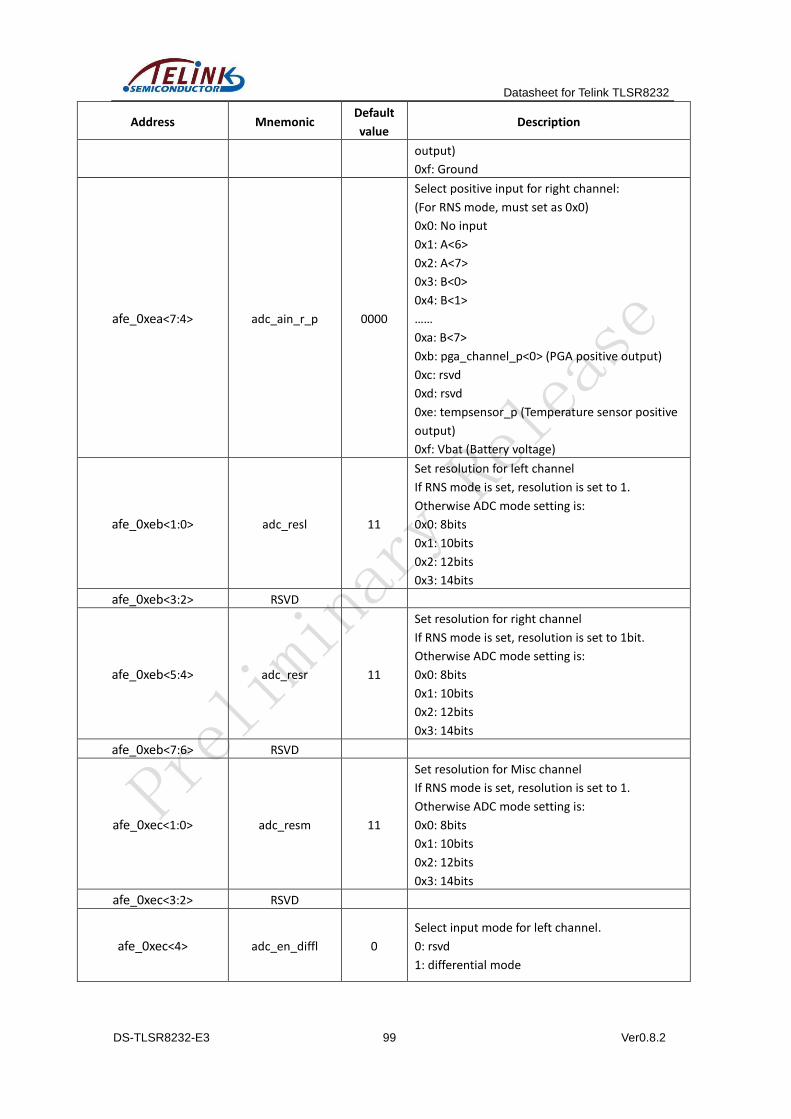
Datasheet for Telink TLSR8232
DS-TLSR8232-E3 99 Ver0.8.2
Address Mnemonic Default
value Description
output)
0xf: Ground
afe_0xea<7:4> adc_ain_r_p 0000
Select positive input for right channel:
(For RNS mode, must set as 0x0)
0x0: No input
0x1: A<6>
0x2: A<7>
0x3: B<0>
0x4: B<1>
……
0xa: B<7>
0xb: pga_channel_p<0> (PGA positive output)
0xc: rsvd
0xd: rsvd
0xe: tempsensor_p (Temperature sensor positive
output)
0xf: Vbat (Battery voltage)
afe_0xeb<1:0> adc_resl 11
Set resolution for left channel
If RNS mode is set, resolution is set to 1.
Otherwise ADC mode setting is:
0x0: 8bits
0x1: 10bits
0x2: 12bits
0x3: 14bits
afe_0xeb<3:2> RSVD
afe_0xeb<5:4> adc_resr 11
Set resolution for right channel
If RNS mode is set, resolution is set to 1bit.
Otherwise ADC mode setting is:
0x0: 8bits
0x1: 10bits
0x2: 12bits
0x3: 14bits
afe_0xeb<7:6> RSVD
afe_0xec<1:0> adc_resm 11
Set resolution for Misc channel
If RNS mode is set, resolution is set to 1.
Otherwise ADC mode setting is:
0x0: 8bits
0x1: 10bits
0x2: 12bits
0x3: 14bits
afe_0xec<3:2> RSVD
afe_0xec<4> adc_en_diffl 0
Select input mode for left channel.
0: rsvd
1: differential mode
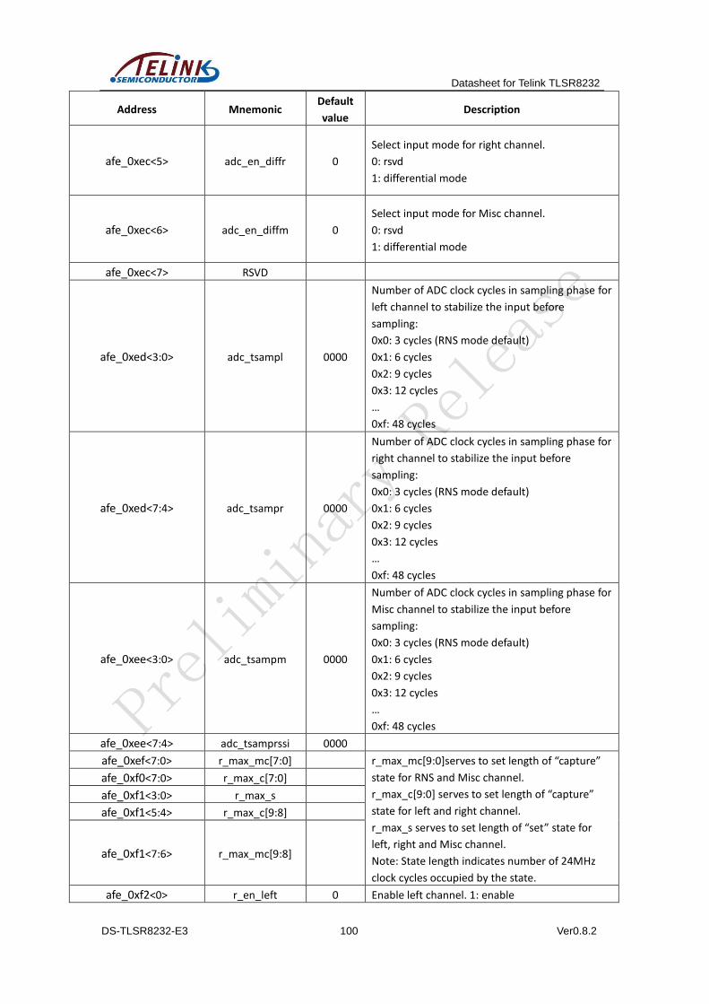
Datasheet for Telink TLSR8232
DS-TLSR8232-E3 100 Ver0.8.2
Address Mnemonic Default
value Description
afe_0xec<5> adc_en_diffr 0
Select input mode for right channel.
0: rsvd
1: differential mode
afe_0xec<6> adc_en_diffm 0
Select input mode for Misc channel.
0: rsvd
1: differential mode
afe_0xec<7> RSVD
afe_0xed<3:0> adc_tsampl 0000
Number of ADC clock cycles in sampling phase for
left channel to stabilize the input before
sampling:
0x0: 3 cycles (RNS mode default)
0x1: 6 cycles
0x2: 9 cycles
0x3: 12 cycles
…
0xf: 48 cycles
afe_0xed<7:4> adc_tsampr 0000
Number of ADC clock cycles in sampling phase for
right channel to stabilize the input before
sampling:
0x0: 3 cycles (RNS mode default)
0x1: 6 cycles
0x2: 9 cycles
0x3: 12 cycles
…
0xf: 48 cycles
afe_0xee<3:0> adc_tsampm 0000
Number of ADC clock cycles in sampling phase for
Misc channel to stabilize the input before
sampling:
0x0: 3 cycles (RNS mode default)
0x1: 6 cycles
0x2: 9 cycles
0x3: 12 cycles
…
0xf: 48 cycles
afe_0xee<7:4> adc_tsamprssi 0000
afe_0xef<7:0> r_max_mc[7:0]
r_max_mc[9:0]serves to set length of “capture”
state for RNS and Misc channel.
r_max_c[9:0] serves to set length of “capture”
state for left and right channel.
r_max_s serves to set length of “set” state for
left, right and Misc channel.
Note: State length indicates number of 24MHz
clock cycles occupied by the state.
afe_0xf0<7:0> r_max_c[7:0]
afe_0xf1<3:0> r_max_s
afe_0xf1<5:4> r_max_c[9:8]
afe_0xf1<7:6> r_max_mc[9:8]
afe_0xf2<0> r_en_left 0 Enable left channel. 1: enable
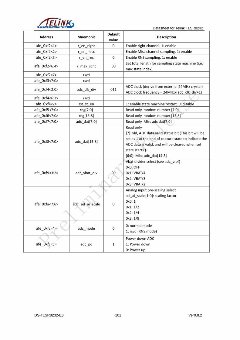
Datasheet for Telink TLSR8232
DS-TLSR8232-E3 101 Ver0.8.2
Address Mnemonic Default
value Description
afe_0xf2<1> r_en_right 0 Enable right channel. 1: enable
afe_0xf2<2> r_en_misc
Enable Misc channel sampling. 1: enable
afe_0xf2<3> r_en_rns 0 Enable RNS sampling. 1: enable
afe_0xf2<6:4> r_max_scnt 00 Set total length for sampling state machine (i.e.
max state index)
afe_0xf2<7> rsvd
afe_0xf3<7:0> rsvd
afe_0xf4<2:0> adc_clk_div 011 ADC clock (derive from external 24MHz crystal)
ADC clock frequency = 24MHz/(adc_clk_div+1)
afe_0xf4<6:3> rsvd
afe_0xf4<7> rst_st_en 1: enable state machine restart, 0: disable
afe_0xf5<7:0> rng[7:0]
Read only, random number [7:0]
afe_0xf6<7:0> rng[15:8]
Read only, random number [15:8]
afe_0xf7<7:0> adc_dat[7:0]
Read only, Misc adc dat[7:0]
afe_0xf8<7:0> adc_dat[15:8]
Read only
[7]: vld, ADC data valid status bit (This bit will be
set as 1 at the end of capture state to indicate the
ADC data is valid, and will be cleared when set
state starts.)
[6:0]: Misc adc_dat[14:8]
afe_0xf9<3:2> adc_vbat_div 00
Vbat divider select (see adc_vref)
0x0: OFF
0x1: VBAT/4
0x2: VBAT/3
0x3: VBAT/2
afe_0xfa<7:6> adc_sel_ai_scale 0
Analog input pre-scaling select
sel_ai_scale[1:0]: scaling factor
0x0: 1
0x1: 1/2
0x2: 1/4
0x3: 1/8
afe_0xfc<4> adc_mode 0 0: normal mode
1: rsvd (RNS mode)
afe_0xfc<5> adc_pd 1
Power down ADC
1: Power down
0: Power up
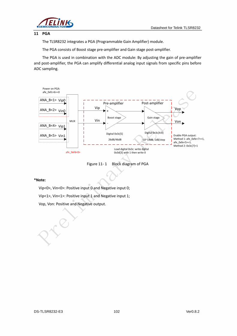
Datasheet for Telink TLSR8232
DS-TLSR8232-E3 102 Ver0.8.2
11 PGA
The TLSR8232 integrates a PGA (Programmable Gain Amplifier) module.
The PGA consists of Boost stage pre-amplifier and Gain stage post-amplifier.
The PGA is used in combination with the ADC module: By adjusting the gain of pre-amplifier
and post-amplifier, the PGA can amplify differential analog input signals from specific pins before
ADC sampling.
Pre-amplifier Post-amplifier
afe_0xfd<0>
Boost stage Gain stage
26dB/46dB -10~14dB, 1dB/step
Vop
Von
+
-
Power on PGA: afe_0xfc<6>=0
MUX
ANA_B<1>
ANA_B<2> Vip
Vin
Vip0
Vin0
ANA_B<4>
ANA_B<5>
Vip1
Vin1Digital 0x3c[5] Digital 0x3c[4:0]
Load digital 0x3c: write digital 0x3d[3] with 1 then write 0
Enable PGA output:Method 1: afe_0xfe<7>=1, afe_0xfe<5>=1. Method 2: 0x3c[7]=1
Figure 11- 1 Block diagram of PGA
*Note:
Vip<0>, Vin<0>: Positive input 0 and Negative input 0;
Vip<1>, Vin<1>: Positive input 1 and Negative input 1;
Vop, Von: Positive and Negative output.
Datasheet for Telink TLSR8232
DS-TLSR8232-E3 103 Ver0.8.2
11.1 Power on/down
The PGA is disabled by default.
To power on the PGA, the analog register pga_pd (afe_0xfc<6>) should be set as 1b’0.
11.2 Select input channel
The PGA differential input is selectable via the analog register pga_sel_vin (afe_0xfd<0>).
If afe_0xfd<0> is set as 1b’0, ANA_B<1> and ANA_B<2> are selected as positive and negative
input, respectively.
If afe_0xfd<0> is set as 1b’1, ANA_B<4> and ANA_B<5> are selected as positive and negative
input, respectively.
11.3 Adjust gain
The PGA gain is adjustable via digital register 0x3c:
Address 0x3c[5] serves to set gain for the pre-amplifier as 26dB or 46dB.
Address 0x3c[4:0] serves to set gain for the post-amplifier as -10dB (0x0) ~ 14dB (0x18) with
step of 1dB.
The total PGA gain should be the sum of the two gain values.
11.4 Enable/Disable PGA output
User can enable/disable PGA output by using either analog registers or digital register.
Use analog register “pga_mute_m_en” (afe_0xfe<7>) and “pga_mute_m” (afe_0xfe<5>). User
can enable PGA output by setting both afe_0xfe<7> and afe_0xfe<5> as 1b’1.
Use digital register 0x3c[7]. User can also enable PGA output by setting 0x3c[7] as 1b’1.
Digital register 0x3d[4] indicates whether PGA output is enabled or disabled.
11.5 Load digital register 0x3c
User should write digital register 0x3d[3] with 1b’1 and 1b’0 to load the value of digital
register 0x3c, so that the configuration of 0x3c can take effect.
Datasheet for Telink TLSR8232
DS-TLSR8232-E3 104 Ver0.8.2
11.6 Register table
Table 11- 1 Analog register table related to PGA
Address Mnemonic Default Description
Analog register
afe_0xfc<6> pga_pd 1 Power down PGA
1: Power down, 0: Power up
afe_0xfd<0> pga_sel_vin 0
Select PGA differential input source.
Gate off all input with pga_pd.
0: select ANA_B<1> (positive) and
ANA_B<2> (negative)
1: select ANA_B<4> (positive) and
ANA_B<5> (negative)
afe_0xfe<7> pga_mute_m_en 0
Enable using analog register
pga_mute_m
0: disable using analog register
afe_0xfe<5>
1: enable using analog register
afe_0xfe<5>
afe_0xfe<5> pga_mute_m 0
When afe_0xfe<7> = 0x1, this bit can
be used
0: not mute pga
1: mute pga
Digital register
0x3c 0x00
[4:0]: set gain for the post-amplifier
0x0~0x18: -10dB~14dB, step 1dB
[5]: set gain for the pre-amplifier
0: 26dB, 1: 46dB
[7]: mute PGA using digital register
0x3d 0x00
[3]: write 1 and then write 0 to trigger
PGA load 0x3c value
[4]: read only indicate PGA mute
release status
0: not release
1: release
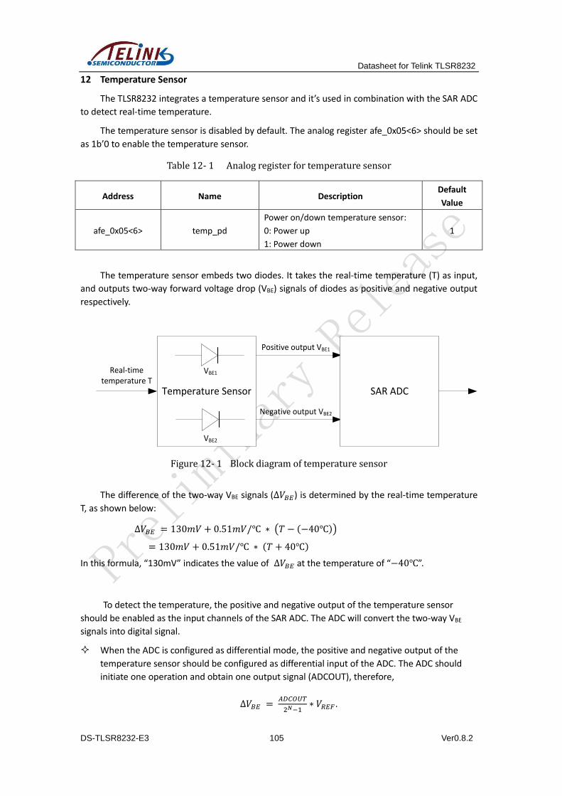
Datasheet for Telink TLSR8232
DS-TLSR8232-E3 105 Ver0.8.2
12 Temperature Sensor
The TLSR8232 integrates a temperature sensor and it’s used in combination with the SAR ADC
to detect real-time temperature.
The temperature sensor is disabled by default. The analog register afe_0x05<6> should be set
as 1b’0 to enable the temperature sensor.
Table 12- 1 Analog register for temperature sensor
Address Name Description Default
Value
afe_0x05<6> temp_pd
Power on/down temperature sensor:
0: Power up
1: Power down
1
The temperature sensor embeds two diodes. It takes the real-time temperature (T) as input,
and outputs two-way forward voltage drop (VBE) signals of diodes as positive and negative output
respectively.
Temperature Sensor
Real-time temperature T
Positive output VBE1
Negative output VBE2
VBE1
VBE2
SAR ADC
Differential or single-end mode
Figure 12- 1 Block diagram of temperature sensor
The difference of the two-way VBE signals (∆𝑉𝐵𝐸) is determined by the real-time temperature
T, as shown below:
∆𝑉𝐵𝐸 = 130𝑚𝑉 + 0.51𝑚𝑉/℃ ∗ (𝑇 − (−40℃))
= 130𝑚𝑉 + 0.51𝑚𝑉/℃ ∗ (𝑇 + 40℃)
In this formula, “130mV” indicates the value of ∆𝑉𝐵𝐸 at the temperature of “−40℃”.
To detect the temperature, the positive and negative output of the temperature sensor
should be enabled as the input channels of the SAR ADC. The ADC will convert the two-way VBE
signals into digital signal.
When the ADC is configured as differential mode, the positive and negative output of the
temperature sensor should be configured as differential input of the ADC. The ADC should
initiate one operation and obtain one output signal (ADCOUT), therefore,
∆𝑉𝐵𝐸 = 𝐴𝐷𝐶𝑂𝑈𝑇
2𝑁−1∗ 𝑉𝑅𝐸𝐹.
Datasheet for Telink TLSR8232
DS-TLSR8232-E3 106 Ver0.8.2
In the formula, “N” and “𝑉𝑅𝐸𝐹” indicates the selected resolution and reference voltage of the
SAR ADC.
Then the real-time temperature T can be calculated according to the ∆𝑉𝐵𝐸 .
Datasheet for Telink TLSR8232
DS-TLSR8232-E3 107 Ver0.8.2
13 AES
The TLSR8232 embeds AES module with encryption and decryption function. The input
128bit plaintext in combination of key is converted into the final output ciphertext via encryption;
the 128bit ciphertext in combination of key can also be converted into 128bit plaintext via
decryption.
The AES hardware accelerator provides automatic encryption and decryption. It only takes
(1000*system clock cycles) to implement AES encryption/decryption. Suppose system clock is
20MHz, the time needed for AES encryption/decryption is 50us.
13.1 RISC mode
For RISC mode, configuration of related registers is as follows:
1) Set the value of key via writing registers AES_KEY0~ AES_KEY15 (address 0x550~0x55f).
2) Set operation method of AES module via register AES_CTRL: set address 0x540[0] as 1b’1
for decryption method, while clear this bit for encryption method.
3) For encryption method, write registers AES-DAT0~ AES-DAT3 (address 0x548~0x54b) for
four times to set the 128bit plaintext. After encryption, the 128bit ciphertext can be
obtained by reading address 0x548~0x54b for four times.
4) For decryption method, write registers AES-DAT0~ AES-DAT3 (address 0x548~0x54b) for
four times to set the 128bit ciphertext. After decryption, the 128bit plaintext can be
obtained by reading address 0x548~0x54b for four times.
5) Address 0x540 bit[1] and bit[2] are read only bits: bit[1] will be cleared automatically
after quartic writing of address 0x548~0x54b; bit[2] will be set as 1 automatically after
encryption/decryption, and then cleared automatically after quartic reading of address
0x548~0x54b.
13.2 AES-CCM
The AES-CCM (Counter with the CBC-MAC) mode is disabled by default. AES output is
directly determined by current encryption and decryption, irrespective of previous encryption and
decryption result.
If 0x540[7] is set as 1b’1 to enable AES-CCM mode, AES output will also take previous
encryption and decryption result into consideration.
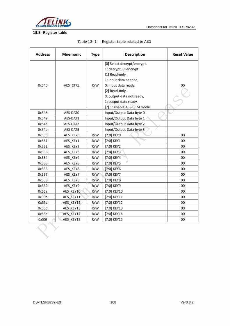
Datasheet for Telink TLSR8232
DS-TLSR8232-E3 108 Ver0.8.2
13.3 Register table
Table 13- 1 Register table related to AES
Address Mnemonic Type Description Reset Value
0x540 AES_CTRL R/W
[0] Select decrypt/encrypt.
1: decrypt, 0: encrypt
[1] Read-only.
1: input data needed,
0: input data ready.
[2] Read-only.
0: output data not ready,
1: output data ready.
[7] 1: enable AES-CCM mode.
00
0x548 AES-DAT0 Input/Output Data byte 0
0x549 AES-DAT1 Input/Output Data byte 1
0x54a AES-DAT2 Input/Output Data byte 2
0x54b AES-DAT3 Input/Output Data byte 3
0x550 AES_KEY0 R/W [7:0] KEY0 00
0x551 AES_KEY1 R/W [7:0] KEY1 00
0x552 AES_KEY2 R/W [7:0] KEY2 00
0x553 AES_KEY3 R/W [7:0] KEY3 00
0x554 AES_KEY4 R/W [7:0] KEY4 00
0x555 AES_KEY5 R/W [7:0] KEY5 00
0x556 AES_KEY6 R/W [7:0] KEY6 00
0x557 AES_KEY7 R/W [7:0] KEY7 00
0x558 AES_KEY8 R/W [7:0] KEY8 00
0x559 AES_KEY9 R/W [7:0] KEY9 00
0x55a AES_KEY10 R/W [7:0] KEY10 00
0x55b AES_KEY11 R/W [7:0] KEY11 00
0x55c AES_KEY12 R/W [7:0] KEY12 00
0x55d AES_KEY13 R/W [7:0] KEY13 00
0x55e AES_KEY14 R/W [7:0] KEY14 00
0x55f AES_KEY15 R/W [7:0] KEY15 00
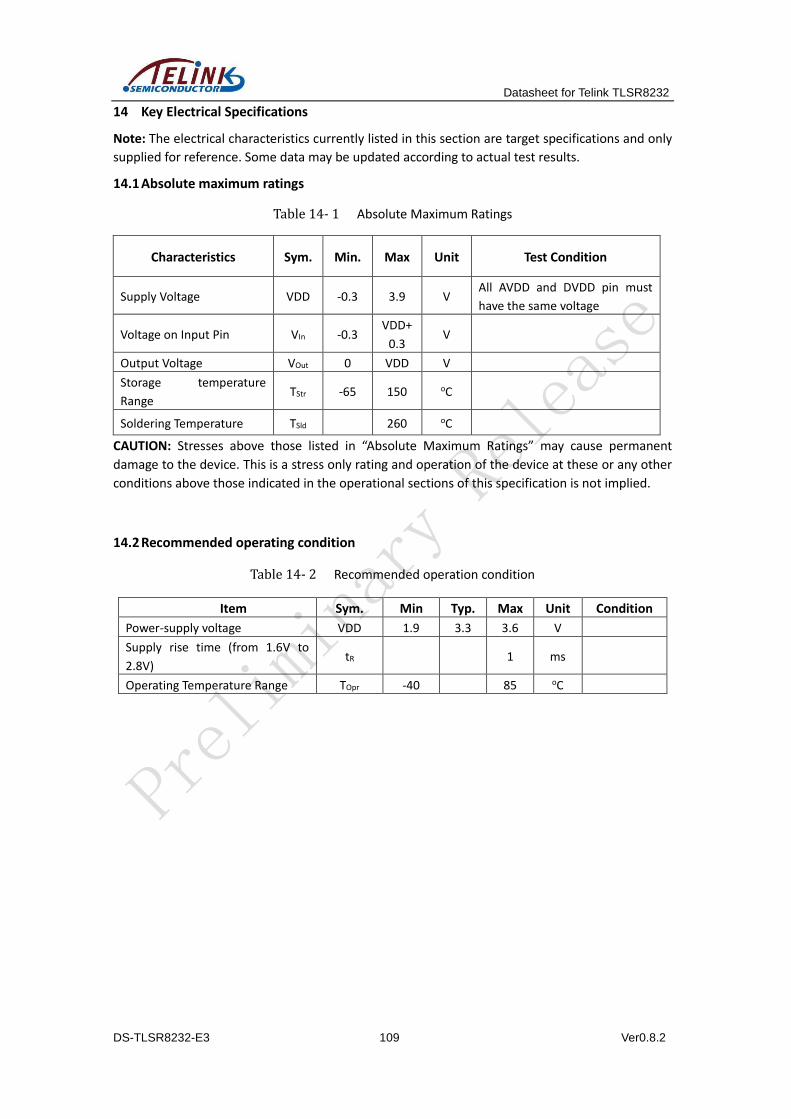
Datasheet for Telink TLSR8232
DS-TLSR8232-E3 109 Ver0.8.2
14 Key Electrical Specifications
Note: The electrical characteristics currently listed in this section are target specifications and only
supplied for reference. Some data may be updated according to actual test results.
14.1 Absolute maximum ratings
Table 14- 1 Absolute Maximum Ratings
Characteristics Sym. Min. Max Unit Test Condition
Supply Voltage VDD -0.3 3.9 V All AVDD and DVDD pin must
have the same voltage
Voltage on Input Pin VIn -0.3 VDD+
0.3 V
Output Voltage VOut 0 VDD V
Storage temperature
Range TStr -65 150 oC
Soldering Temperature TSld 260 oC
CAUTION: Stresses above those listed in “Absolute Maximum Ratings” may cause permanent
damage to the device. This is a stress only rating and operation of the device at these or any other
conditions above those indicated in the operational sections of this specification is not implied.
14.2 Recommended operating condition
Table 14- 2 Recommended operation condition
Item Sym. Min Typ. Max Unit Condition
Power-supply voltage VDD 1.9 3.3 3.6 V
Supply rise time (from 1.6V to
2.8V) tR 1 ms
Operating Temperature Range TOpr -40 85 oC
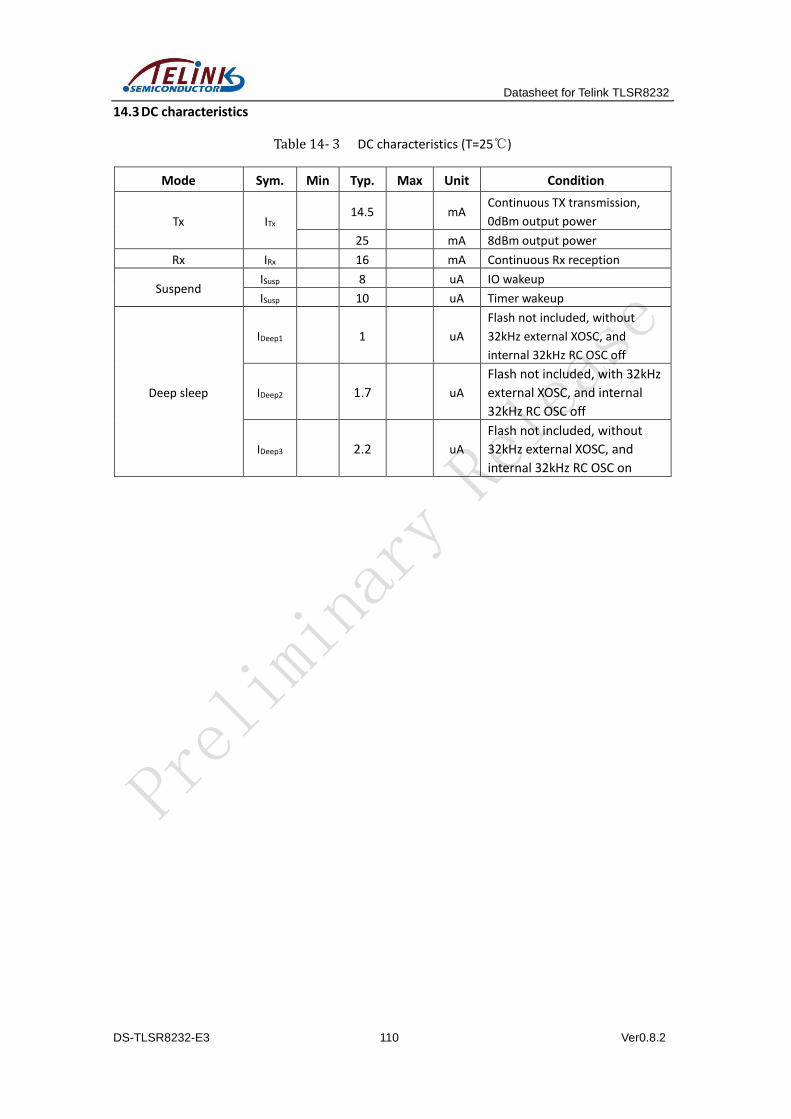
Datasheet for Telink TLSR8232
DS-TLSR8232-E3 110 Ver0.8.2
14.3 DC characteristics
Table 14- 3 DC characteristics (T=25℃)
Mode Sym. Min Typ. Max Unit Condition
Tx ITx 14.5 mA
Continuous TX transmission,
0dBm output power
25 mA 8dBm output power
Rx IRx 16 mA Continuous Rx reception
Suspend ISusp 8 uA IO wakeup
ISusp 10 uA Timer wakeup
Deep sleep
IDeep1 1 uA
Flash not included, without
32kHz external XOSC, and
internal 32kHz RC OSC off
IDeep2 1.7 uA
Flash not included, with 32kHz
external XOSC, and internal
32kHz RC OSC off
IDeep3 2.2 uA
Flash not included, without
32kHz external XOSC, and
internal 32kHz RC OSC on
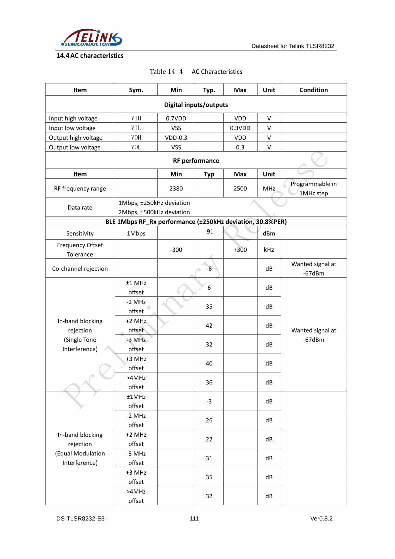
Datasheet for Telink TLSR8232
DS-TLSR8232-E3 111 Ver0.8.2
14.4 AC characteristics
Table 14- 4 AC Characteristics
Item Sym. Min Typ. Max Unit Condition
Digital inputs/outputs
Input high voltage VIH 0.7VDD VDD V
Input low voltage VIL VSS 0.3VDD V
Output high voltage VOH VDD-0.3 VDD V
Output low voltage VOL VSS 0.3 V
RF performance
Item Min Typ Max Unit
RF frequency range
2380 2500 MHz Programmable in
1MHz step
Data rate 1Mbps, ±250kHz deviation
2Mbps, ±500kHz deviation
BLE 1Mbps RF_Rx performance (±250kHz deviation, 30.8%PER)
Sensitivity 1Mbps -91 dBm
Frequency Offset
Tolerance -300 +300 kHz
Co-channel rejection -6 dB Wanted signal at
-67dBm
In-band blocking
rejection
(Single Tone
Interference)
±1 MHz
offset 6 dB
Wanted signal at
-67dBm
-2 MHz
offset 35 dB
+2 MHz
offset 42 dB
-3 MHz
offset 32 dB
+3 MHz
offset 40 dB
>4MHz
offset 36 dB
In-band blocking
rejection
(Equal Modulation
Interference)
±1MHz
offset -3 dB
-2 MHz
offset 26 dB
+2 MHz
offset 22 dB
-3 MHz
offset 31 dB
+3 MHz
offset 35 dB
>4MHz
offset 32 dB
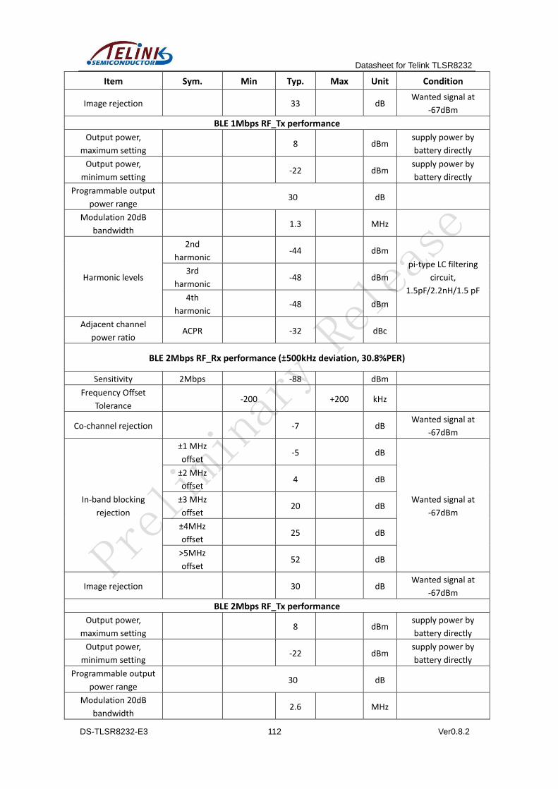
Datasheet for Telink TLSR8232
DS-TLSR8232-E3 112 Ver0.8.2
Item Sym. Min Typ. Max Unit Condition
Image rejection 33 dB Wanted signal at
-67dBm
BLE 1Mbps RF_Tx performance
Output power,
maximum setting 8 dBm
supply power by
battery directly
Output power,
minimum setting -22 dBm
supply power by
battery directly
Programmable output
power range 30 dB
Modulation 20dB
bandwidth 1.3 MHz
Harmonic levels
2nd
harmonic -44 dBm
pi-type LC filtering
circuit,
1.5pF/2.2nH/1.5 pF
3rd
harmonic -48 dBm
4th
harmonic -48 dBm
Adjacent channel
power ratio ACPR -32 dBc
BLE 2Mbps RF_Rx performance (±500kHz deviation, 30.8%PER)
Sensitivity 2Mbps -88 dBm
Frequency Offset
Tolerance -200 +200 kHz
Co-channel rejection -7 dB Wanted signal at
-67dBm
In-band blocking
rejection
±1 MHz
offset -5 dB
Wanted signal at
-67dBm
±2 MHz
offset 4 dB
±3 MHz
offset 20 dB
±4MHz
offset 25 dB
>5MHz
offset 52 dB
Image rejection 30 dB Wanted signal at
-67dBm
BLE 2Mbps RF_Tx performance
Output power,
maximum setting 8 dBm
supply power by
battery directly
Output power,
minimum setting -22 dBm
supply power by
battery directly
Programmable output
power range 30 dB
Modulation 20dB
bandwidth 2.6 MHz
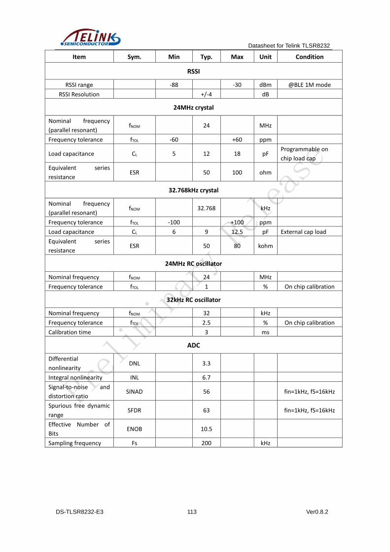
Datasheet for Telink TLSR8232
DS-TLSR8232-E3 113 Ver0.8.2
Item Sym. Min Typ. Max Unit Condition
RSSI
RSSI range -88 -30 dBm @BLE 1M mode
RSSI Resolution +/-4 dB
24MHz crystal
Nominal frequency
(parallel resonant) fNOM
24
MHz
Frequency tolerance fTOL -60 +60 ppm
Load capacitance CL 5 12 18 pF Programmable on
chip load cap
Equivalent series
resistance ESR 50 100 ohm
32.768kHz crystal
Nominal frequency
(parallel resonant) fNOM
32.768 kHz
Frequency tolerance fTOL -100 +100 ppm
Load capacitance CL 6 9 12.5 pF External cap load
Equivalent series
resistance ESR
50 80 kohm
24MHz RC oscillator
Nominal frequency fNOM 24 MHz
Frequency tolerance fTOL 1 % On chip calibration
32kHz RC oscillator
Nominal frequency fNOM 32 kHz
Frequency tolerance fTOL 2.5 % On chip calibration
Calibration time 3 ms
ADC
Differential
nonlinearity DNL 3.3
Integral nonlinearity INL 6.7
Signal-to-noise and
distortion ratio SINAD 56 fin=1kHz, fS=16kHz
Spurious free dynamic
range SFDR 63 fin=1kHz, fS=16kHz
Effective Number of
Bits ENOB 10.5
Sampling frequency Fs 200 kHz
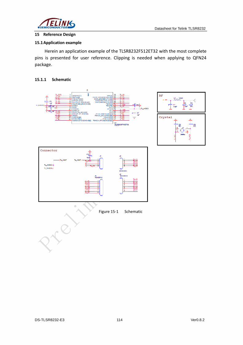
Datasheet for Telink TLSR8232
DS-TLSR8232-E3 114 Ver0.8.2
15 Reference Design
15.1 Application example
Herein an application example of the TLSR8232F512ET32 with the most complete
pins is presented for user reference. Clipping is needed when applying to QFN24
package.
15.1.1 Schematic
Figure 15-1 Schematic
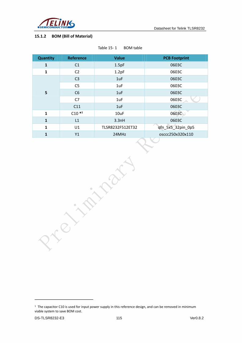
Datasheet for Telink TLSR8232
DS-TLSR8232-E3 115 Ver0.8.2
15.1.2 BOM (Bill of Material)
Table 15- 1 BOM table
Quantity Reference Value PCB Footprint
1 C1 1.5pF 0603C
1 C2 1.2pF 0603C
5
C3 1uF 0603C
C5 1uF 0603C
C6 1uF 0603C
C7 1uF 0603C
C11 1uF 0603C
1 C10 *1 10uF 0603C
1 L1 3.3nH 0603C
1 U1 TLSR8232F512ET32 qfn_5x5_32pin_0p5
1 Y1 24MHz osccc250x320x110
1 The capacitor C10 is used for input power supply in this reference design, and can be removed in minimum viable system to save BOM cost.