datasheet - iis2iclx - high-accuracy, high-resolution, low-power, 2 … · 1 overview the iis2iclx...
TRANSCRIPT

Ceramic cavity LGA-16(5 x 5 x 1.7 mm)
Features• 2-axis linear accelerometer• Selectable full scale: ±0.5/±1/±2/±3 g• Ultra-low noise performance: 15 µg/√Hz• Superior stability over temperature (<0.075 mg/°C) and repeatability• Embedded compensation for high stability over temperature• I²C/SPI digital output interface• Low power: 0.42 mA with 2 axes delivering full performance• Sensor hub feature to efficiently collect data from additional external sensors• Smart embedded FIFO up to 3 kbytes• Programmable high-pass and low-pass digital filters• Programmable Machine Learning Core to integrate AI algorithms and reduce
power consumption at system level• Programmable Finite State Machine to process data from accelerometer and
one external sensor• Extended operating temperature range (-40 °C to +105 °C)• Embedded temperature sensor• Analog supply voltage: 1.71 V to 3.6 V• High shock survivability• ECOPACK, RoHS and "Green" compliant
Applications• Precision inclinometers• Antenna pointing and platform leveling• Structural health monitoring• Precise leveling instruments• Installation and monitoring of equipment• Robotics and industrial automation
DescriptionThe IIS2ICLX is a high-accuracy (ultra-low noise, high stability and repeatability) andlow-power two-axis linear accelerometer with digital output.
The IIS2ICLX has a selectable full scale of ±0.5/±1/±2/±3 g and is capable ofproviding the measured accelerations to the application over an I²C or SPI digitalinterface.
Its high accuracy, stability over temperature and repeatability make IIS2ICLXparticularly suitable for inclination measurement applications (inclinometers).
The sensing element is manufactured using a dedicated micromachining processdeveloped by STMicroelectronics to produce inertial sensors and actuators on siliconwafers.
The IC interface is manufactured using a CMOS process that allows a high level ofintegration to design a dedicated circuit which is trimmed to better match thecharacteristics of the sensing element.
Product status link
IIS2ICLX
Product summary
Order code IIS2ICLXTR
Temperaturerange [°C] -40 to +105
Package CC LGA-16(5 x 5 x 1.7 mm)
Packing Tape and reel
Product labels
High-accuracy, high-resolution, low-power, 2-axis digital inclinometer with embedded Machine Learning Core
IIS2ICLX
Datasheet
DS13005 - Rev 3 - June 2020For further information contact your local STMicroelectronics sales office.
www.st.com
The IIS2ICLX has an unmatched set of embedded features (programmable FSM,Machine Learning Core, sensor hub, FIFO, event decoding and interrupts) which areenablers for implementing smart and complex sensor nodes which deliver highaccuracy and performance at very low power.
The IIS2ICLX is available in a high-performance (low-stress) ceramic cavity land gridarray (CC LGA) package and can operate within a temperature range of -40 °C to+105 °C.
IIS2ICLX
DS13005 - Rev 3 page 2/122

1 Overview
The IIS2ICLX is a high-accuracy (ultra-low noise, high stability and repeatability) and ultra-low-power two-axisdigital accelerometer specifically recommended for inclination measurements (inclinometers) in Industry 4.0applications.All design aspects and the testing and calibration of the IIS2ICLX have been optimized to reach superioraccuracy, stability, repeatability and extremely low noise.The IIS2ICLX has a selectable full scale of ±0.5/±1/±2/±3 g and is capable of providing the measuredaccelerations to the application over an I²C or SPI digital interface.Its unique set of embedded features (programmable FSM, Machine Learning Core, sensor hub, FIFO, eventdecoding and interrupts) facilitate the implementation of smart and complex sensor nodes which deliver highaccuracy at very low power.Like the entire portfolio of ST MEMS sensors, the IIS2ICLX leverages the robust and mature in-housemanufacturing processes already used for the production of micromachined accelerometers and gyroscopes. Thevarious sensing elements are manufactured using specialized micromachining processes, while the IC interfacesare developed using CMOS technology that allows the design of a dedicated circuit which is trimmed to bettermatch the characteristics of the sensing element.The IIS2ICLX is available in a high-performance (low-stress) ceramic cavity land grid array (CC LGA) packageand can operate within a temperature range of -40 °C to +105 °C.
Note: Due to the use of epoxy glue for lid sealing, hermeticity of the package is not guaranteed. Processing or use ofthis package in a harsh environment should be assessed by the customer.
IIS2ICLXOverview
DS13005 - Rev 3 page 3/122
2 Embedded low-power features
The IIS2ICLX features the following on-chip functions:• 3 kbytes data buffering
– 100% efficiency with flexible configurations and partitioning– Possibility to store timestamp and external sensors
• Event-detection interrupts (fully configurable)– Wakeup– Click and double-click sensing– Stationary/Motion detection
• Specific IP blocks with negligible power consumption and high-performance– Finite State Machine for accelerometer and external sensors– Machine Learning Core
• Sensor hub– Up to 5 total sensors: internal accelerometer and 4 external sensors
IIS2ICLXEmbedded low-power features
DS13005 - Rev 3 page 4/122
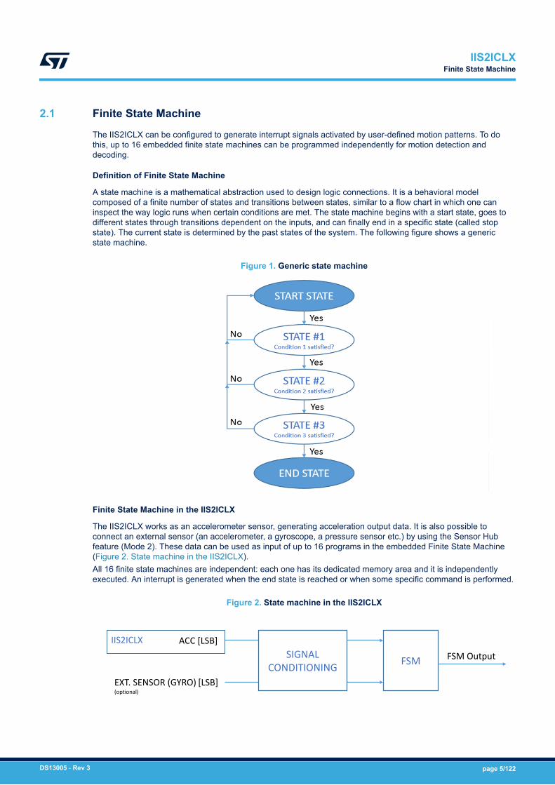
2.1 Finite State Machine
The IIS2ICLX can be configured to generate interrupt signals activated by user-defined motion patterns. To dothis, up to 16 embedded finite state machines can be programmed independently for motion detection anddecoding.
Definition of Finite State Machine
A state machine is a mathematical abstraction used to design logic connections. It is a behavioral modelcomposed of a finite number of states and transitions between states, similar to a flow chart in which one caninspect the way logic runs when certain conditions are met. The state machine begins with a start state, goes todifferent states through transitions dependent on the inputs, and can finally end in a specific state (called stopstate). The current state is determined by the past states of the system. The following figure shows a genericstate machine.
Figure 1. Generic state machine
Finite State Machine in the IIS2ICLX
The IIS2ICLX works as an accelerometer sensor, generating acceleration output data. It is also possible toconnect an external sensor (an accelerometer, a gyroscope, a pressure sensor etc.) by using the Sensor Hubfeature (Mode 2). These data can be used as input of up to 16 programs in the embedded Finite State Machine(Figure 2. State machine in the IIS2ICLX).All 16 finite state machines are independent: each one has its dedicated memory area and it is independentlyexecuted. An interrupt is generated when the end state is reached or when some specific command is performed.
Figure 2. State machine in the IIS2ICLX
ACC [LSB]
EXT. SENSOR (GYRO) [LSB](optional)
IIS2ICLXSIGNAL
CONDITIONING FSM FSM Output
IIS2ICLXFinite State Machine
DS13005 - Rev 3 page 5/122

2.2 Machine Learning Core
The IIS2ICLX embeds a dedicated core for machine learning processing that provides system flexibility, allowingsome algorithms run in the application processor to be moved to the MEMS sensor with the advantage ofconsistent reduction in power consumption.Machine Learning Core logic allows identifying if a data pattern (for example motion, pressure, temperature,magnetic data, etc.) matches a user-defined set of classes. Typical examples of applications could be anomalousvibration recognition, complex movement or condition identification, activity detection, etc.The IIS2ICLX Machine Learning Core works on data patterns coming from the accelerometer, but it is alsopossible to connect and process external sensor data (from a gyroscope or additional external inclinometer/accelerometer, temperature or pressure sensors) by using the Sensor Hub feature (Mode 2).The input data can be filtered using a dedicated configurable computation block containing filters and featurescomputed in a fixed time window defined by the user.Machine learning processing is based on logical processing composed of a series of configurable nodescharacterized by "if-then-else" conditions where the "feature" values are evaluated against defined thresholds.
Figure 3. Machine Learning Core in the IIS2ICLX
INPUT Sensor Data & Hub
Machine Learning Core OUTPUT
Accelerometer Results
External Sensor Features
Filters
Interrupts
Machine Learning Core
Logical processing
The IIS2ICLX can be configured to run up to 8 flows simultaneously and independently and every flow cangenerate up to 256 results. The total number of nodes can be up to 512.The results of the machine learning processing are available in dedicated output registers readable from theapplication processor at any time.The IIS2ICLX Machine Learning Core can be configured to generate an interrupt when a change in the resultoccurs.
IIS2ICLXMachine Learning Core
DS13005 - Rev 3 page 6/122

3 Pin description
Figure 4. Pin connections
X
Y
(TOP VIEW)DIRECTION OF THE DETECTABLE ACCELERATIONS
1
TOP VIEW
2
1
16
15
3
14 13 12 11
4
10
9
8
7
65
3.1 Pin connections
The IIS2ICLX offers flexibility to connect the pins in order to have two different mode connections andfunctionalities. In detail:• Mode 1: I²C slave interface or SPI (3- and 4-wire) serial interface is available;• Mode 2: I²C slave interface or SPI (3- and 4-wire) serial interface and I²C interface master for external
sensor connections are available.
Figure 5. IIS2ICLX connection modes
HOST
IIS2ICLX
HOST
IIS2ICLX
LSM6DSMLSM6DSMExternal sensors
I2C /SPI (3/4-w)
I2C /SPI (3/4-w)
Master I2C
Mode 1 Mode 2
In the following table each mode is described for the pin connections and function.
IIS2ICLXPin description
DS13005 - Rev 3 page 7/122

Table 1. Pin description
Pin number Name Mode 1 function Mode 2 function
1 VDD_IO Power supply for I/O pins (recommended 100 nF filter capacitor)
2 CS
I²C/SPI mode selection
(1: SPI idle mode / I²C communication enabled;
0: SPI communication mode / I²C disabled and reset)
3 GND 0 V supply
4 INT2Programmable interrupt 2 (INT2) /
Data enable (DEN)
Programmable interrupt 2 (INT2) /
Data enable (DEN)/I²C master external synchronization signal (MDRDY)
5 SDO/SA0SPI 4-wire serial data output (SDO)
I²C least significant bit of the device address (SA0)
6 INT1 Programmable Interrupt 1 (INT1)
7 SDx Connect to GND or VDD_IO I²C serial data master (MSDA)
8 VDD Power supply (recommended 100 nF filter capacitor)
9 VDD Power supply (recommended 100 nF filter capacitor)
10 SCLI²C serial clock (SCL)
SPI serial port clock (SPC)
11 SDA/SDI
I²C serial data (SDA)
SPI serial data input (SDI)
3-wire interface serial data output (SDO)
12 SCx Connect to GND or VDD_IO I²C serial clock master (MSCL)
13 GND GND
14 NC Connect to GND or leave unconnected
15 NC Connect to GND or leave unconnected
16 NC Connect to GND or leave unconnected
IIS2ICLXPin connections
DS13005 - Rev 3 page 8/122
4 Module specifications
4.1 Mechanical characteristics
@ Vdd = 3.0 V, T = 25 °C, unless otherwise noted.
Table 2. Mechanical characteristics
Symbol Parameter Test conditions Min.(1) Typ.(2) Max.(1) Unit
FS Measurement range
±0.5
g±1.0
±2.0
±3.0
So Sensitivity(3)
FS = ±0.5
-2%
0.015
+2% mg/LSBFS = ±1.0 0.031
FS = ±2.0 0.061
FS = ±3.0 0.122
So_acc Sensitivity change over life(4) -1.5 ±0.7 +1.5 %
TCSo Sensitivity change vs. temperature From -40° to +105°C,delta from 25 °C -0.012 ±0.01 +0.012 %/°C
Off Zero-g level offset accuracy(5) -8 +8 mg
Off_acc Zero-g level change over life(4) -2.5 ±1 +2.5 mg
TCOff Zero-g level change vs. temperature From -40° to +105°C, delta from 25 °C -0.075 ±0.020 +0.075 mg/°C
NL Non-linearity Best-fit straight line 0.1 % FS
An Zero-g noise density 15 30 µg/√Hz
ODR Digital output data rate
12.5
26
52
104
208
416
833
Hz
Bw Bandwidth @ODR 833 Hz 260 Hz
VRE Vibration rectification error FS = ±2 g; ODR = 50 Hz;2.5 grms vibration in 50 - 2000 Hz band 1 mg
F0 Sensor resonant frequency 900 Hz
ST Self-test @FS = ±2 g 1 15 mg
Top Operating temperature range -40 +105 °C
1. Min/Max values are based on characterization results at 3σ on a limited number of samples, not tested inproduction and not guaranteed.
2. Typical specifications are not guaranteed.3. Sensitivity range after MSL3 preconditioning.4. Drift over life assessed based on behavior after 1000h of THS (Temperature Humidity Storage) at T=+85°C /
RH = 85%.5. Typical zero-g level offset value after MSL3 preconditioning.
IIS2ICLXModule specifications
DS13005 - Rev 3 page 9/122
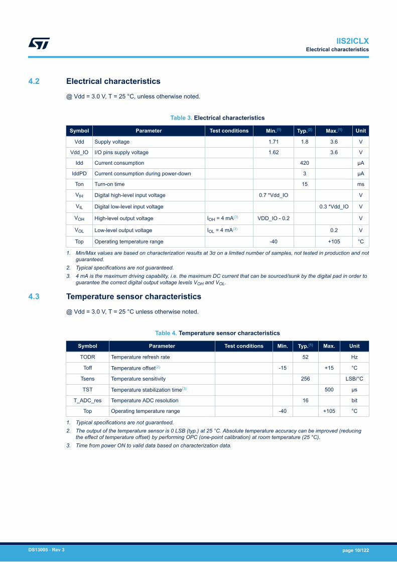
4.2 Electrical characteristics
@ Vdd = 3.0 V, T = 25 °C, unless otherwise noted.
Table 3. Electrical characteristics
Symbol Parameter Test conditions Min.(1) Typ.(2) Max.(1) Unit
Vdd Supply voltage 1.71 1.8 3.6 V
Vdd_IO I/O pins supply voltage 1.62 3.6 V
Idd Current consumption 420 µA
IddPD Current consumption during power-down 3 µA
Ton Turn-on time 15 ms
VIH Digital high-level input voltage 0.7 *Vdd_IO V
VIL Digital low-level input voltage 0.3 *Vdd_IO V
VOH High-level output voltage IOH = 4 mA(3) VDD_IO - 0.2 V
VOL Low-level output voltage IOL = 4 mA(3) 0.2 V
Top Operating temperature range -40 +105 °C
1. Min/Max values are based on characterization results at 3σ on a limited number of samples, not tested in production and notguaranteed.
2. Typical specifications are not guaranteed.3. 4 mA is the maximum driving capability, i.e. the maximum DC current that can be sourced/sunk by the digital pad in order to
guarantee the correct digital output voltage levels VOH and VOL.
4.3 Temperature sensor characteristics
@ Vdd = 3.0 V, T = 25 °C unless otherwise noted.
Table 4. Temperature sensor characteristics
Symbol Parameter Test conditions Min. Typ.(1) Max. Unit
TODR Temperature refresh rate 52 Hz
Toff Temperature offset(2) -15 +15 °C
Tsens Temperature sensitivity 256 LSB/°C
TST Temperature stabilization time(3) 500 µs
T_ADC_res Temperature ADC resolution 16 bit
Top Operating temperature range -40 +105 °C
1. Typical specifications are not guaranteed.2. The output of the temperature sensor is 0 LSB (typ.) at 25 °C. Absolute temperature accuracy can be improved (reducing
the effect of temperature offset) by performing OPC (one-point calibration) at room temperature (25 °C).3. Time from power ON to valid data based on characterization data.
IIS2ICLXElectrical characteristics
DS13005 - Rev 3 page 10/122
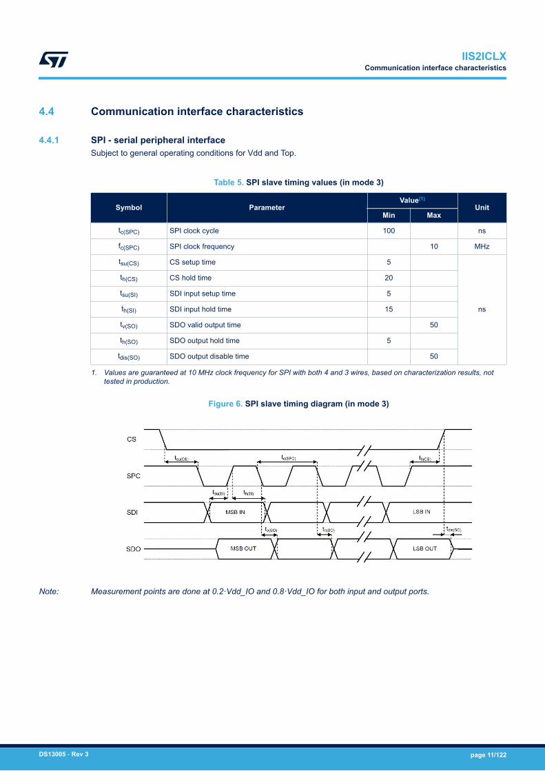
4.4 Communication interface characteristics
4.4.1 SPI - serial peripheral interfaceSubject to general operating conditions for Vdd and Top.
Table 5. SPI slave timing values (in mode 3)
Symbol ParameterValue(1)
UnitMin Max
tc(SPC) SPI clock cycle 100 ns
fc(SPC) SPI clock frequency 10 MHz
tsu(CS) CS setup time 5
ns
th(CS) CS hold time 20
tsu(SI) SDI input setup time 5
th(SI) SDI input hold time 15
tv(SO) SDO valid output time 50
th(SO) SDO output hold time 5
tdis(SO) SDO output disable time 50
1. Values are guaranteed at 10 MHz clock frequency for SPI with both 4 and 3 wires, based on characterization results, nottested in production.
Figure 6. SPI slave timing diagram (in mode 3)
Note: Measurement points are done at 0.2·Vdd_IO and 0.8·Vdd_IO for both input and output ports.
IIS2ICLXCommunication interface characteristics
DS13005 - Rev 3 page 11/122
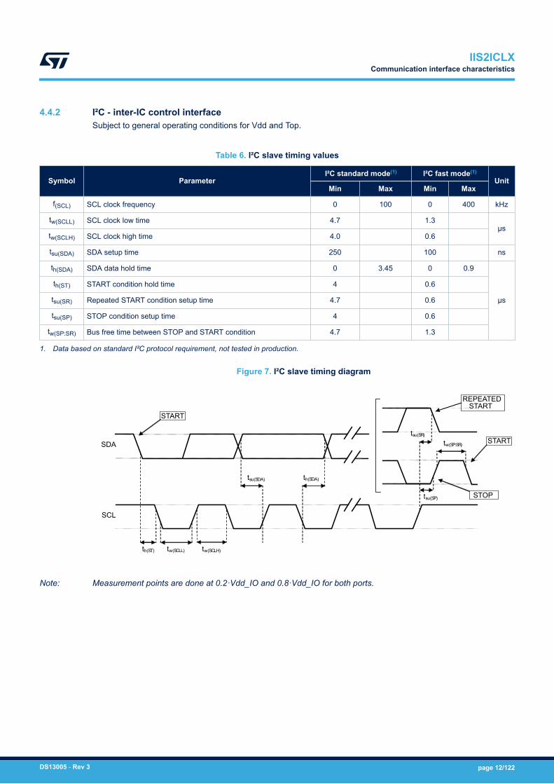
4.4.2 I²C - inter-IC control interfaceSubject to general operating conditions for Vdd and Top.
Table 6. I²C slave timing values
Symbol ParameterI²C standard mode(1) I²C fast mode(1)
UnitMin Max Min Max
f(SCL) SCL clock frequency 0 100 0 400 kHz
tw(SCLL) SCL clock low time 4.7 1.3µs
tw(SCLH) SCL clock high time 4.0 0.6
tsu(SDA) SDA setup time 250 100 ns
th(SDA) SDA data hold time 0 3.45 0 0.9
µs
th(ST) START condition hold time 4 0.6
tsu(SR) Repeated START condition setup time 4.7 0.6
tsu(SP) STOP condition setup time 4 0.6
tw(SP:SR) Bus free time between STOP and START condition 4.7 1.3
1. Data based on standard I²C protocol requirement, not tested in production.
Figure 7. I²C slave timing diagram
tsu(SP)
tw(SCLL)
tsu(SDA)
tsu(SR)
th(ST) tw(SCLH)
th(SDA)
tw(SP:SR)
REPEATEDSTART
START
STOP
START
SDA
SCL
Note: Measurement points are done at 0.2·Vdd_IO and 0.8·Vdd_IO for both ports.
IIS2ICLXCommunication interface characteristics
DS13005 - Rev 3 page 12/122
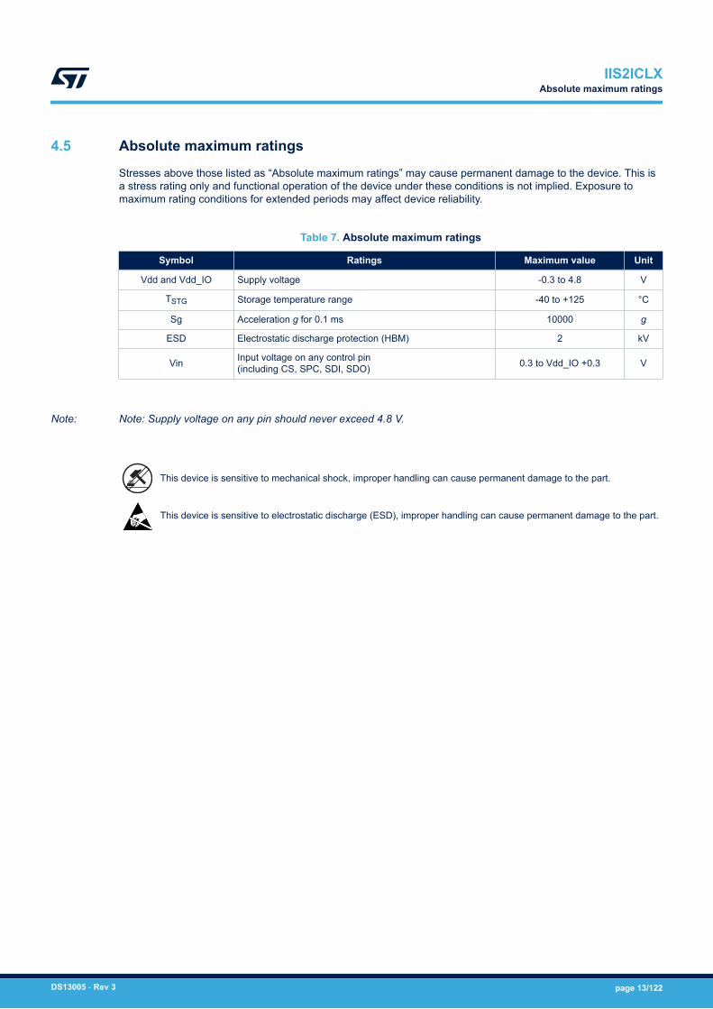
4.5 Absolute maximum ratings
Stresses above those listed as “Absolute maximum ratings” may cause permanent damage to the device. This isa stress rating only and functional operation of the device under these conditions is not implied. Exposure tomaximum rating conditions for extended periods may affect device reliability.
Table 7. Absolute maximum ratings
Symbol Ratings Maximum value Unit
Vdd and Vdd_IO Supply voltage -0.3 to 4.8 V
TSTG Storage temperature range -40 to +125 °C
Sg Acceleration g for 0.1 ms 10000 g
ESD Electrostatic discharge protection (HBM) 2 kV
Vin Input voltage on any control pin(including CS, SPC, SDI, SDO) 0.3 to Vdd_IO +0.3 V
Note: Note: Supply voltage on any pin should never exceed 4.8 V.
This device is sensitive to mechanical shock, improper handling can cause permanent damage to the part.
This device is sensitive to electrostatic discharge (ESD), improper handling can cause permanent damage to the part.
IIS2ICLXAbsolute maximum ratings
DS13005 - Rev 3 page 13/122

5 Digital interfaces
5.1 I²C/SPI interface
The registers embedded inside the IIS2ICLX may be accessed through both the I²C and SPI serial interfaces. Thelatter may be SW configured to operate either in 3-wire or 4-wire interface mode. The device is compatible withSPI modes 0 and 3.The serial interfaces are mapped onto the same pins. To select/exploit the I²C interface, the CS line must be tiedhigh (i.e connected to Vdd_IO).
Table 8. Serial interface pin description
Pin name Pin description
CS
SPI enable
I²C/SPI mode selection (1: SPI idle mode / I²C communication enabled;
0: SPI communication mode / I²C disabled)
SCL/SPCI²C Serial Clock (SCL)
SPI Serial Port Clock (SPC)
SDA/SDI/SDO
I²C Serial Data (SDA)
SPI Serial Data Input (SDI)
3-wire Interface Serial Data Output (SDO)
SDO/SA0SPI Serial Data Output (SDO)
I²C less significant bit of the device address
5.2 I²C serial interface
The IIS2ICLX I²C is a bus slave. The I²C is employed to write the data to the registers, whose content can also beread back.The relevant I²C terminology is provided in the table below.
Table 9. I²C terminology
Term Description
Transmitter The device which sends data to the bus
Receiver The device which receives data from the bus
Master The device which initiates a transfer, generates clock signals and terminates a transfer
Slave The device addressed by the master
There are two signals associated with the I²C bus: the serial clock line (SCL) and the Serial DAta line (SDA). Thelatter is a bidirectional line used for sending and receiving the data to/from the interface. Both the lines must beconnected to Vdd_IO through external pull-up resistors. When the bus is free, both the lines are high.The I²C interface is implemeted with fast mode (400 kHz) I²C standards as well as with the standard mode.In order to disable the I²C block, (I2C_disable) = 1 must be written in CTRL4_C (13h).
IIS2ICLXDigital interfaces
DS13005 - Rev 3 page 14/122

5.2.1 I²C operationThe transaction on the bus is started through a START (ST) signal. A START condition is defined as a HIGH toLOW transition on the data line while the SCL line is held HIGH. After this has been transmitted by the master, thebus is considered busy. The next byte of data transmitted after the start condition contains the address of theslave in the first 7 bits and the eighth bit tells whether the master is receiving data from the slave or transmittingdata to the slave. When an address is sent, each device in the system compares the first seven bits after a startcondition with its address. If they match, the device considers itself addressed by the master.The Slave ADdress (SAD) associated to the IIS2ICLX is 110101xb. The SDO/SA0 pin can be used to modify theless significant bit of the device address. If the SDO/SA0 pin is connected to the supply voltage, LSb is ‘1’(address 1101011b); else if the SDO/SA0 pin is connected to ground, the LSb value is ‘0’ (address 1101010b).This solution permits to connect and address two different inertial modules to the same I²C bus.Data transfer with acknowledge is mandatory. The transmitter must release the SDA line during the acknowledgepulse. The receiver must then pull the data line LOW so that it remains stable low during the HIGH period of theacknowledge clock pulse. A receiver which has been addressed is obliged to generate an acknowledge after eachbyte of data received.The I²C embedded inside the IIS2ICLX behaves like a slave device and the following protocol must be adheredto. After the start condition (ST) a slave address is sent, once a slave acknowledge (SAK) has been returned, an8-bit sub-address (SUB) is transmitted. The increment of the address is configured by CTRL3_C (12h) (IF_INC).The slave address is completed with a Read/Write bit. If the bit is ‘1’ (Read), a repeated START (SR) conditionmust be issued after the two sub-address bytes; if the bit is ‘0’ (Write) the master will transmit to the slave withdirection unchanged. Table 10 explains how the SAD+Read/Write bit pattern is composed, listing all the possibleconfigurations.
Table 10. SAD+Read/Write patterns
Command SAD[6:1] SAD[0] = SA0 R/W SAD+R/W
Read 110101 0 1 11010101 (D5h)
Write 110101 0 0 11010100 (D4h)
Read 110101 1 1 11010111 (D7h)
Write 110101 1 0 11010110 (D6h)
Table 11. Transfer when master is writing one byte to slave
Master ST SAD + W SUB DATA SP
Slave SAK SAK SAK
Table 12. Transfer when master is writing multiple bytes to slave
Master ST SAD + W SUB DATA DATA SP
Slave SAK SAK SAK SAK
Table 13. Transfer when master is receiving (reading) one byte of data from slave
Master ST SAD + W SUB SR SAD + R NMAK SP
Slave SAK SAK SAK DATA
Table 14. Transfer when master is receiving (reading) multiple bytes of data from slave
Master ST SAD+W SUB SR SAD+R MAK MAK NMAK SP
Slave SAK SAK SAK DATA DATA DATA
IIS2ICLXI²C serial interface
DS13005 - Rev 3 page 15/122
Data are transmitted in byte format (DATA). Each data transfer contains 8 bits. The number of bytes transferredper transfer is unlimited. Data is transferred with the Most Significant bit (MSb) first. If a slave receiver doesn’tacknowledge the slave address (i.e. it is not able to receive because it is performing some real-time function) thedata line must be left HIGH by the slave. The master can then abort the transfer. A LOW to HIGH transition on theSDA line while the SCL line is HIGH is defined as a STOP condition. Each data transfer must be terminated bythe generation of a STOP (SP) condition.In the presented communication format MAK is Master acknowledge and NMAK is No Master Acknowledge.
IIS2ICLXI²C serial interface
DS13005 - Rev 3 page 16/122
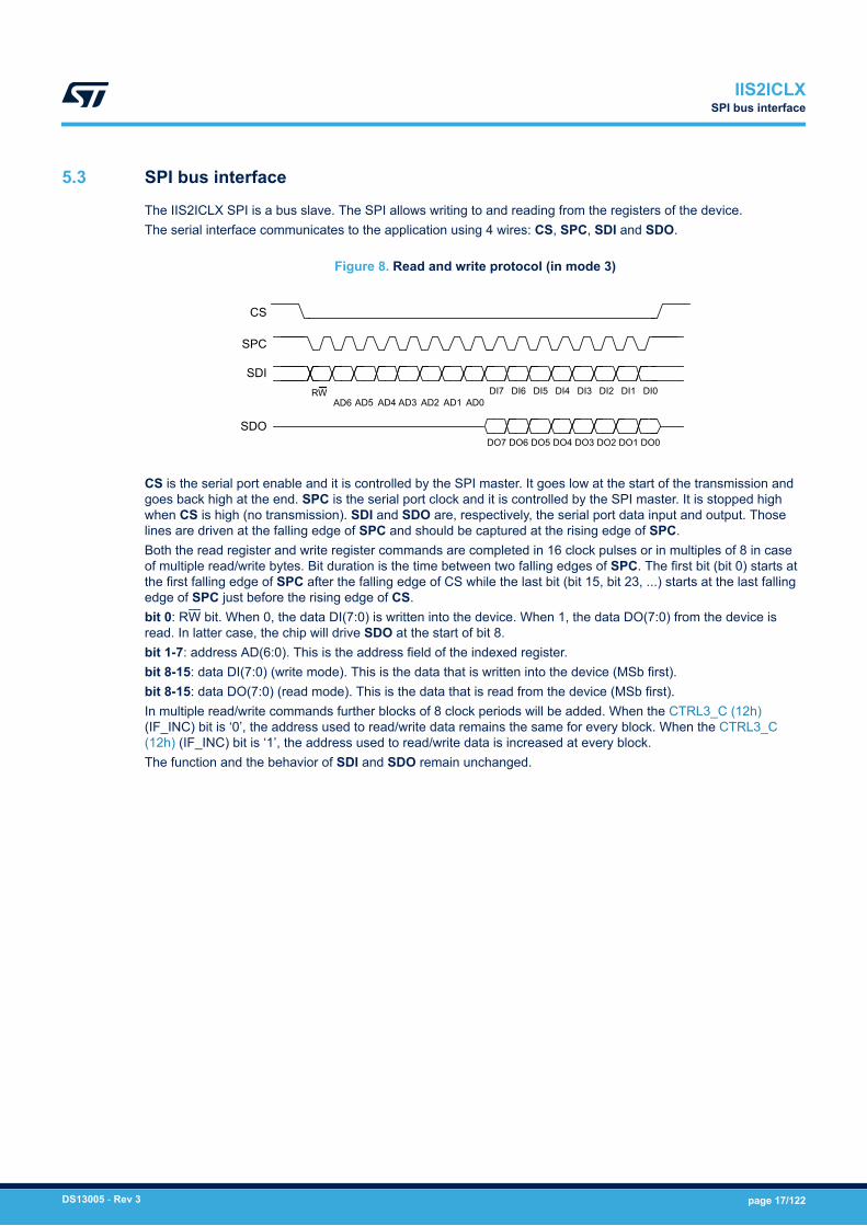
5.3 SPI bus interface
The IIS2ICLX SPI is a bus slave. The SPI allows writing to and reading from the registers of the device.The serial interface communicates to the application using 4 wires: CS, SPC, SDI and SDO.
Figure 8. Read and write protocol (in mode 3)
CS
SPC
SDI
SDO
RWAD5 AD4 AD3 AD2 AD1 AD0
DI7 DI6 DI5 DI4 DI3 DI2 DI1 DI0
DO7 DO6 DO5 DO4 DO3 DO2 DO1 DO0
AD6
CS is the serial port enable and it is controlled by the SPI master. It goes low at the start of the transmission andgoes back high at the end. SPC is the serial port clock and it is controlled by the SPI master. It is stopped highwhen CS is high (no transmission). SDI and SDO are, respectively, the serial port data input and output. Thoselines are driven at the falling edge of SPC and should be captured at the rising edge of SPC.Both the read register and write register commands are completed in 16 clock pulses or in multiples of 8 in caseof multiple read/write bytes. Bit duration is the time between two falling edges of SPC. The first bit (bit 0) starts atthe first falling edge of SPC after the falling edge of CS while the last bit (bit 15, bit 23, ...) starts at the last fallingedge of SPC just before the rising edge of CS.bit 0: RW bit. When 0, the data DI(7:0) is written into the device. When 1, the data DO(7:0) from the device isread. In latter case, the chip will drive SDO at the start of bit 8.bit 1-7: address AD(6:0). This is the address field of the indexed register.bit 8-15: data DI(7:0) (write mode). This is the data that is written into the device (MSb first).bit 8-15: data DO(7:0) (read mode). This is the data that is read from the device (MSb first).In multiple read/write commands further blocks of 8 clock periods will be added. When the CTRL3_C (12h)(IF_INC) bit is ‘0’, the address used to read/write data remains the same for every block. When the CTRL3_C(12h) (IF_INC) bit is ‘1’, the address used to read/write data is increased at every block.The function and the behavior of SDI and SDO remain unchanged.
IIS2ICLXSPI bus interface
DS13005 - Rev 3 page 17/122
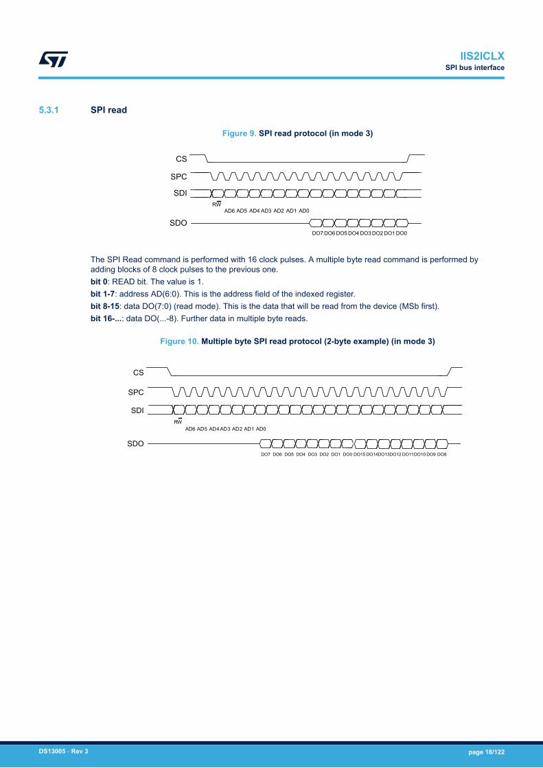
5.3.1 SPI read
Figure 9. SPI read protocol (in mode 3)
CS
SPC
SDI
SDO
RW
DO7 DO6 DO5 DO4 DO3 DO2 DO1 DO0
AD5 AD4 AD3 AD2 AD1 AD0AD6
The SPI Read command is performed with 16 clock pulses. A multiple byte read command is performed byadding blocks of 8 clock pulses to the previous one.bit 0: READ bit. The value is 1.bit 1-7: address AD(6:0). This is the address field of the indexed register.bit 8-15: data DO(7:0) (read mode). This is the data that will be read from the device (MSb first).bit 16-...: data DO(...-8). Further data in multiple byte reads.
Figure 10. Multiple byte SPI read protocol (2-byte example) (in mode 3)
CS
SPC
SDI
SDO
RW
DO7 DO6 DO5 DO4 DO3 DO2 DO1 DO0
AD5 AD4 AD3 AD2 AD1 AD0
DO15 DO14 DO13 DO12 DO11DO10 DO9 DO8
AD6
IIS2ICLXSPI bus interface
DS13005 - Rev 3 page 18/122
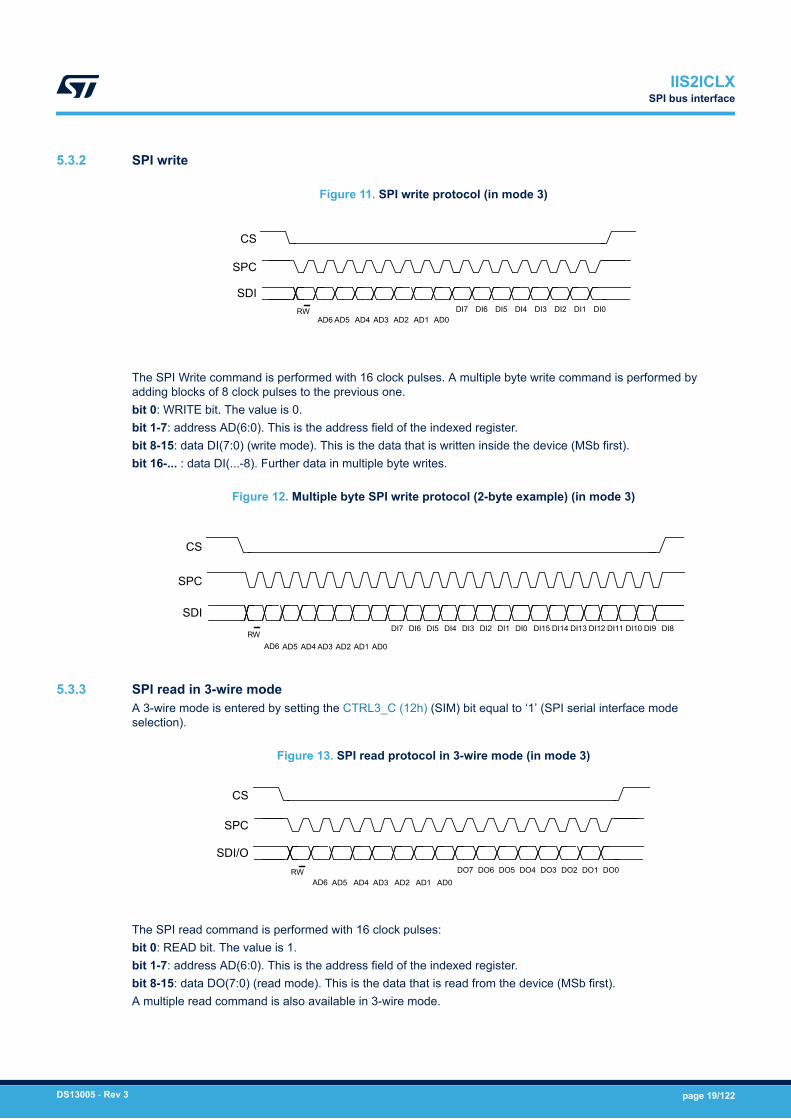
5.3.2 SPI write
Figure 11. SPI write protocol (in mode 3)
CS
SPC
SDIRW DI7 DI6 DI5 DI4 DI3 DI2 DI1 DI0
AD5 AD4 AD3 AD2 AD1 AD0AD6
The SPI Write command is performed with 16 clock pulses. A multiple byte write command is performed byadding blocks of 8 clock pulses to the previous one.bit 0: WRITE bit. The value is 0.bit 1-7: address AD(6:0). This is the address field of the indexed register.bit 8-15: data DI(7:0) (write mode). This is the data that is written inside the device (MSb first).bit 16-... : data DI(...-8). Further data in multiple byte writes.
Figure 12. Multiple byte SPI write protocol (2-byte example) (in mode 3)
CS
SPC
SDI
RWAD5 AD4 AD3 AD2 AD1 AD0
DI7 DI6 DI5 DI4 DI3 DI2 DI1 DI0 DI15 DI14 DI13 DI12 DI11 DI10 DI9 DI8
AD6
5.3.3 SPI read in 3-wire modeA 3-wire mode is entered by setting the CTRL3_C (12h) (SIM) bit equal to ‘1’ (SPI serial interface modeselection).
Figure 13. SPI read protocol in 3-wire mode (in mode 3)
CS
SPC
SDI/ORW DO7 DO6 DO5 DO4 DO3 DO2 DO1 DO0
AD5 AD4 AD3 AD2 AD1 AD0AD6
The SPI read command is performed with 16 clock pulses:bit 0: READ bit. The value is 1.bit 1-7: address AD(6:0). This is the address field of the indexed register.bit 8-15: data DO(7:0) (read mode). This is the data that is read from the device (MSb first).A multiple read command is also available in 3-wire mode.
IIS2ICLXSPI bus interface
DS13005 - Rev 3 page 19/122

5.4 Master I²C interface
If the IIS2ICLX is configured in Mode 2, a master I²C line is available. The master serial interface is mapped to thefollowing dedicated pins.
Table 15. Master I²C pin details
Pin name Pin description
MSCL I²C serial clock master
MSDA I²C serial data master
MDRDY I²C master external synchronization signal
IIS2ICLXMaster I²C interface
DS13005 - Rev 3 page 20/122
6 Functionality
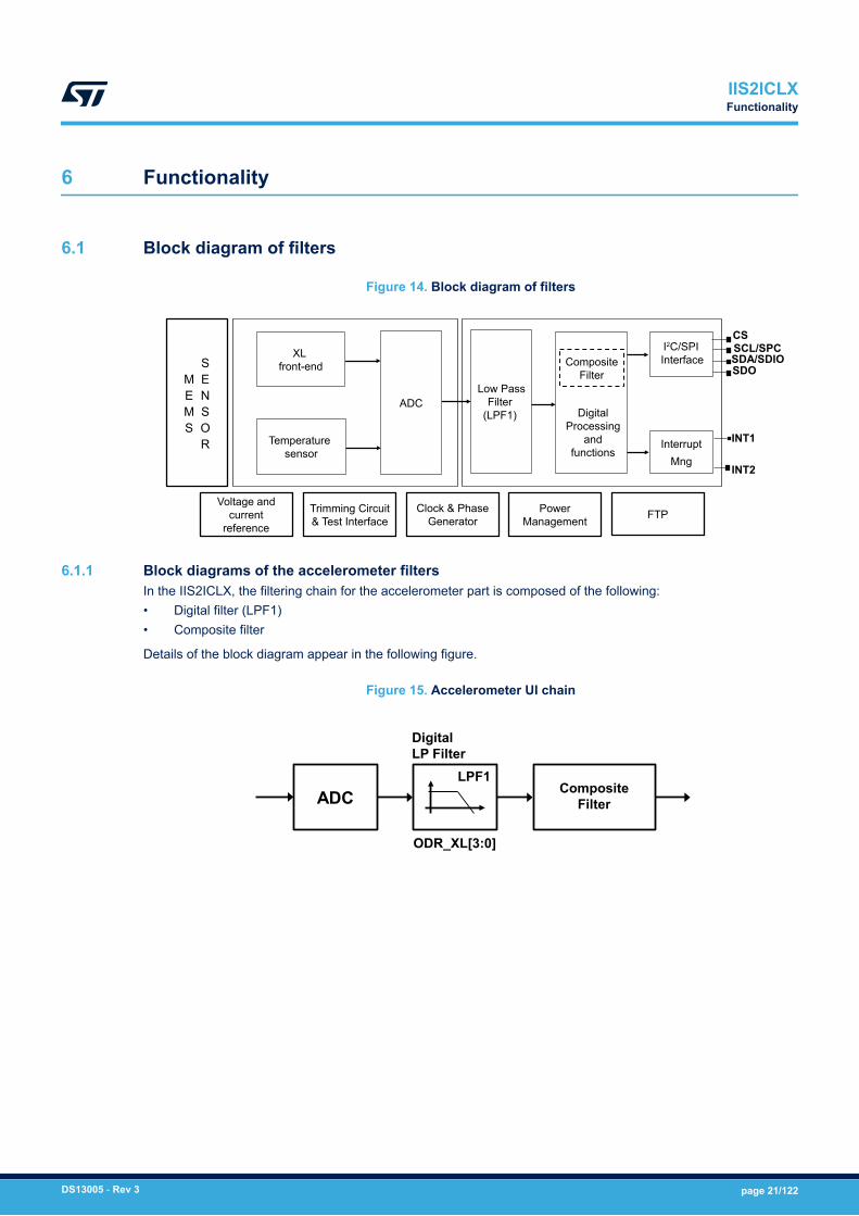
6.1 Block diagram of filters
Figure 14. Block diagram of filters
INT1
Digital Processing
andfunctions
InterruptMng
Low PassFilter
(LPF1)
MEMS
SENSOR
SDA/SDIO
CSSCL/SPC
SDO
INT2
FTPPower Management
Clock & Phase Generator
Trimming Circuit & Test Interface
Voltage and current
reference
I2C/SPI InterfaceComposite
Filter
ADC
XL front-end
Temperature sensor
6.1.1 Block diagrams of the accelerometer filtersIn the IIS2ICLX, the filtering chain for the accelerometer part is composed of the following:• Digital filter (LPF1)• Composite filter
Details of the block diagram appear in the following figure.
Figure 15. Accelerometer UI chain
ADC
DigitalLP Filter
ODR_XL[3:0]
CompositeFilter
LPF1
IIS2ICLXFunctionality
DS13005 - Rev 3 page 21/122
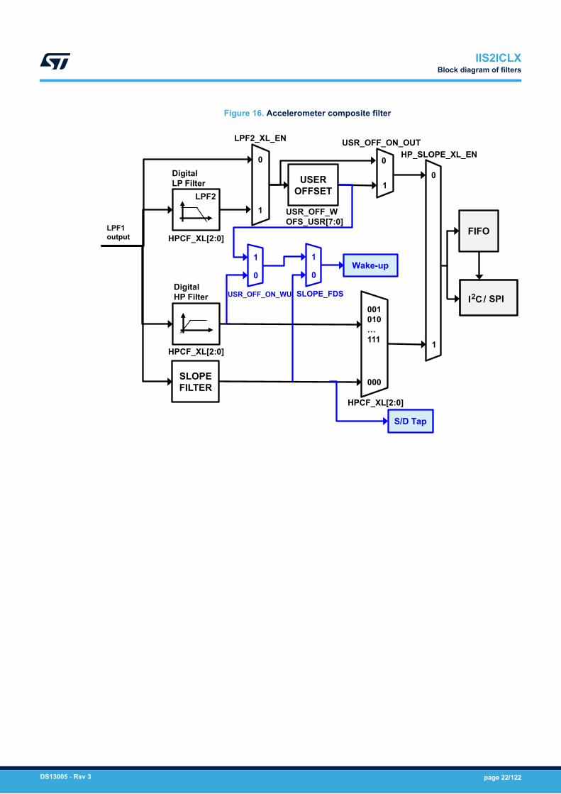
Figure 16. Accelerometer composite filter
SLOPEFILTER
HPCF_XL[2:0]
000
001010…111
SPII2C /
1
0
HP_SLOPE_XL_EN
LPF2_XL_EN
0
1
DigitalHP Filter
HPCF_XL[2:0]
DigitalLP Filter
LPF2
HPCF_XL[2:0]
S/D Tap
1
0
SLOPE_FDS
Wake-up
FIFO
USEROFFSET
0
1
USR_OFF_ON_OUT
USR_OFF_WOFS_USR[7:0]
1
0
USR_OFF_ON_WU
LPF1 output
IIS2ICLXBlock diagram of filters
DS13005 - Rev 3 page 22/122
6.2 FIFO
The presence of a FIFO buffer allows consistent power saving for the system since the host processor does notneed to continuously poll data from the sensor, but it can wake up only when needed and burst the significantdata out from the FIFO.The IIS2ICLX embeds 3 kbytes of data in FIFO to store the following data:• Accelerometer• External sensors (up to 4)• Timestamp• Temperature
The applications have maximum flexibility in choosing the rate of batching for physical sensors with FIFO-dedicated configurations: accelerometer and temperature sensor batch rates can be selected by the user. Writingexternal sensor data in FIFO can be triggered by the accelerometer data-ready signal or by an external sensorinterrupt. It is possible to select decimation for timestamp batching in FIFO with a factor of 1, 8, or 32.The reconstruction of a FIFO stream is a simple task thanks to the FIFO_DATA_OUT_TAG byte that allowsrecognizing the meaning of a word in FIFO.FIFO allows correct reconstruction of the timestamp information for each sensor stored in FIFO. If a change in theODR or BDR (Batch Data Rate) configuration is performed, the application can correctly reconstruct thetimestamp and know exactly when the change was applied without disabling FIFO batching. FIFO storesinformation of the new configuration and timestamp in which the change was applied in the device.The programmable FIFO watermark threshold can be set in FIFO_CTRL1 (07h) and FIFO_CTRL2 (08h) using theWTM[8:0] bits. To monitor the FIFO status, dedicated registers (FIFO_STATUS1 (3Ah), FIFO_STATUS2 (3Bh))can be read to detect FIFO overrun events, FIFO full status, FIFO empty status, FIFO watermark status and thenumber of unread samples stored in the FIFO. To generate dedicated interrupts on the INT1 and INT2 pins ofthese status events, the configuration can be set in INT1_CTRL (0Dh) and INT2_CTRL (0Eh).The FIFO buffer can be configured according to six different modes:• Bypass mode• FIFO mode• Continuous mode• Continuous-to-FIFO mode• Bypass-to-continuous mode• Bypass-to-FIFO mode
Each mode is selected by the FIFO_MODE_[2:0] bits in the FIFO_CTRL4 (0Ah) register.
6.2.1 Bypass modeIn Bypass mode (FIFO_CTRL4 (0Ah)(FIFO_MODE_[2:0] = 000), the FIFO is not operational and it remainsempty. Bypass mode is also used to reset the FIFO when in FIFO mode.
6.2.2 FIFO modeIn FIFO mode (FIFO_CTRL4 (0Ah)(FIFO_MODE_[2:0] = 001) data from the output channels are stored in theFIFO until it is full.To reset FIFO content, Bypass mode should be selected by writing FIFO_CTRL4 (0Ah)(FIFO_MODE_[2:0]) to'000'. After this reset command, it is possible to restart FIFO mode by writing FIFO_CTRL4 (0Ah)(FIFO_MODE_[2:0]) to '001'.The FIFO buffer memorizes up to 3 kbytes of data but the depth of the FIFO can be resized by setting the WTM[8:0] bits in FIFO_CTRL1 (07h) and FIFO_CTRL2 (08h). If the STOP_ON_WTM bit in FIFO_CTRL2 (08h) is set to'1', FIFO depth is limited up to the WTM [8:0] bits inFIFO_CTRL1 (07h) and FIFO_CTRL2 (08h).
IIS2ICLXFIFO
DS13005 - Rev 3 page 23/122
6.2.3 Continuous modeContinuous mode (FIFO_CTRL4 (0Ah)(FIFO_MODE_[2:0] = 110) provides a continuous FIFO update: as newdata arrives, the older data is discarded.A FIFO threshold flag FIFO_STATUS2 (3Bh)(FIFO_WTM_IA) is asserted when the number of unread samples inFIFO is greater than or equal to FIFO_CTRL1 (07h) and FIFO_CTRL2 (08h) (WTM [8:0]).It is possible to route the FIFO_WTM_IA flag to the INT1 pin by writing in register INT1_CTRL (0Dh)(INT1_FIFO_TH) = '1' or to the INT2 pin by writing in register INT2_CTRL (0Eh)(INT2_FIFO_TH) = '1'.A full-flag interrupt can be enabled, INT1_CTRL (0Dh)(INT1_FIFO_FULL) = '1' or INT2_CTRL (0Eh)(INT2_FIFO_FULL) = '1', in order to indicate FIFO saturation and eventually read its content all at once.If an overrun occurs, at least one of the oldest samples in FIFO has been overwritten and the FIFO_OVR_IA flagin FIFO_STATUS2 (3Bh) is asserted.In order to empty the FIFO before it is full, it is also possible to pull from FIFO the number of unread samplesavailable in FIFO_STATUS1 (3Ah) and FIFO_STATUS2 (3Bh)(DIFF_FIFO_[9:0]).
6.2.4 Continuous-to-FIFO modeIn Continuous-to-FIFO mode (FIFO_CTRL4 (0Ah)(FIFO_MODE_[2:0] = 011), FIFO behavior changes accordingto the trigger event detected in one of the following interrupt events:• Single tap• Double tap• Wake-up
When the selected trigger bit is equal to '1', FIFO operates in FIFO mode.When the selected trigger bit is equal to '0', FIFO operates in Continuous mode.
6.2.5 Bypass-to-Continuous modeIn Bypass-to-Continuous mode (FIFO_CTRL4 (0Ah)(FIFO_MODE_[2:0] = '100'), data measurement storageinside FIFO operates in Continuous mode when selected triggers are equal to '1', otherwise FIFO content is reset(Bypass mode).FIFO behavior changes according to the trigger event detected in one of the following interrupt events:• Single tap• Double tap• Wake-up
6.2.6 Bypass-to-FIFO moden Bypass-to-FIFO mode (FIFO_CTRL4 (0Ah)(FIFO_MODE_[2:0] = '111'), data measurement storage inside FIFOoperates in FIFO mode when selected triggers are equal to '1', otherwise FIFO content is reset (Bypass mode).FIFO behavior changes according to the trigger event detected in one of the following interrupt events:• Single tap• Double tap• Wake-up
6.2.7 FIFO reading procedureThe data stored in FIFO are accessible from dedicated registers and each FIFO word is composed of 7 bytes:one tag byte (FIFO_DATA_OUT_TAG (78h), in order to identify the sensor, and 6 bytes of fixed data(FIFO_DATA_OUT registers from (79h) to (7Eh)).The DIFF_FIFO_[9:0] field in the FIFO_STATUS1 (3Ah) and FIFO_STATUS2 (3Bh) registers contains the numberof words (1 byte TAG + 6 bytes DATA) collected in FIFO.In addition, it is possible to configure a counter of the batch events of the accelerometer sensor. The flagCOUNTER_BDR_IA in FIFO_STATUS2 (3Bh) alerts that the counter reaches a selectable threshold(CNT_BDR_TH_[10:0] field in COUNTER_BDR_REG1 (0Bh) and COUNTER_BDR_REG2 (0Ch)). This allowstriggering the reading of FIFO with the desired latency of one single sensor. As for the other FIFO status events,the flag COUNTER_BDR_IA can be routed on the INT1 or INT2 pins by asserting the corresponding bits(INT1_CNT_BDR of INT1_CTRL (0Dh) and INT2_CNT_BDR of INT2_CTRL (0Eh)).Meta information about the accelerometer sensor configuration changes can be managed by enabling theODR_CHG_EN bit in FIFO_CTRL2 (08h).
IIS2ICLXFIFO
DS13005 - Rev 3 page 24/122
7 Frequency response
The IIS2ICLX filtering chain and frequency response are detailed in the following figures.
Figure 17. Filtering chain
MEMS ADC
AnalogFront-end+
ADC
LPF1
Low-Pass Filter
Composite Filter
Composite Filterf0=900Hz
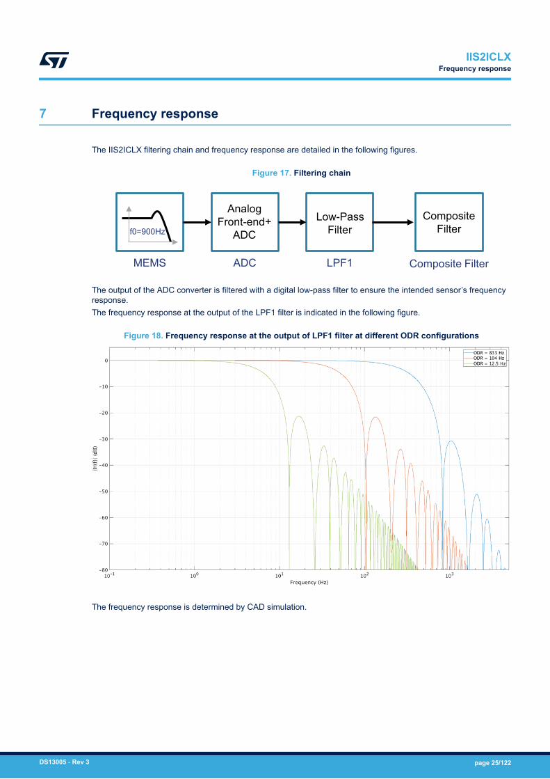
The output of the ADC converter is filtered with a digital low-pass filter to ensure the intended sensor’s frequencyresponse.The frequency response at the output of the LPF1 filter is indicated in the following figure.
Figure 18. Frequency response at the output of LPF1 filter at different ODR configurations
The frequency response is determined by CAD simulation.
IIS2ICLXFrequency response
DS13005 - Rev 3 page 25/122
8 Typical performance characteristics
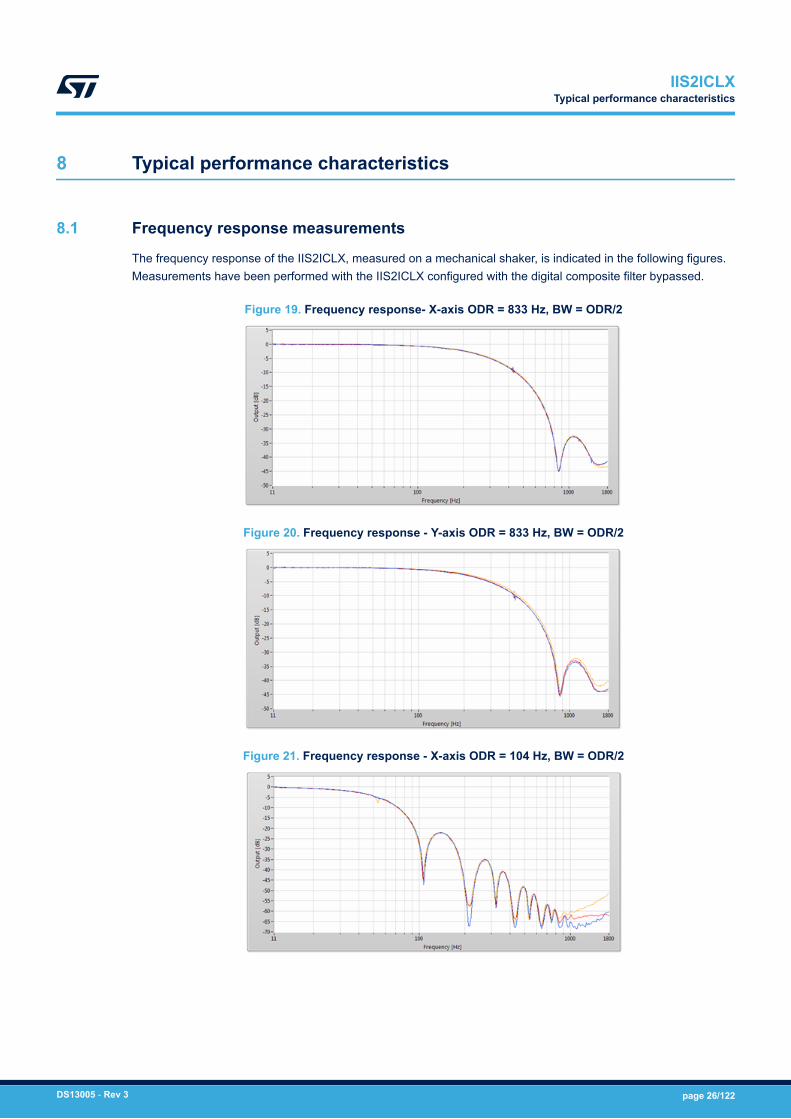
8.1 Frequency response measurements
The frequency response of the IIS2ICLX, measured on a mechanical shaker, is indicated in the following figures.Measurements have been performed with the IIS2ICLX configured with the digital composite filter bypassed.
Figure 19. Frequency response- X-axis ODR = 833 Hz, BW = ODR/2
Figure 20. Frequency response - Y-axis ODR = 833 Hz, BW = ODR/2
Figure 21. Frequency response - X-axis ODR = 104 Hz, BW = ODR/2
IIS2ICLXTypical performance characteristics
DS13005 - Rev 3 page 26/122
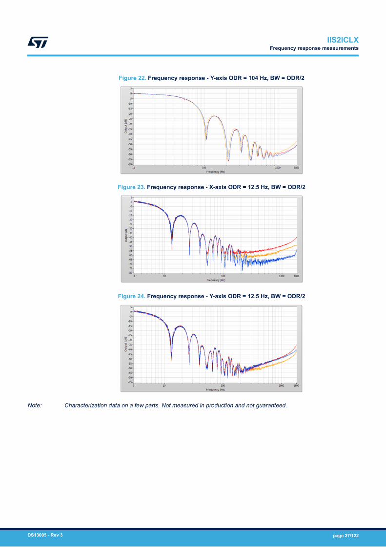
Figure 22. Frequency response - Y-axis ODR = 104 Hz, BW = ODR/2
Figure 23. Frequency response - X-axis ODR = 12.5 Hz, BW = ODR/2
Figure 24. Frequency response - Y-axis ODR = 12.5 Hz, BW = ODR/2
Note: Characterization data on a few parts. Not measured in production and not guaranteed.
IIS2ICLXFrequency response measurements
DS13005 - Rev 3 page 27/122
9 Application hints
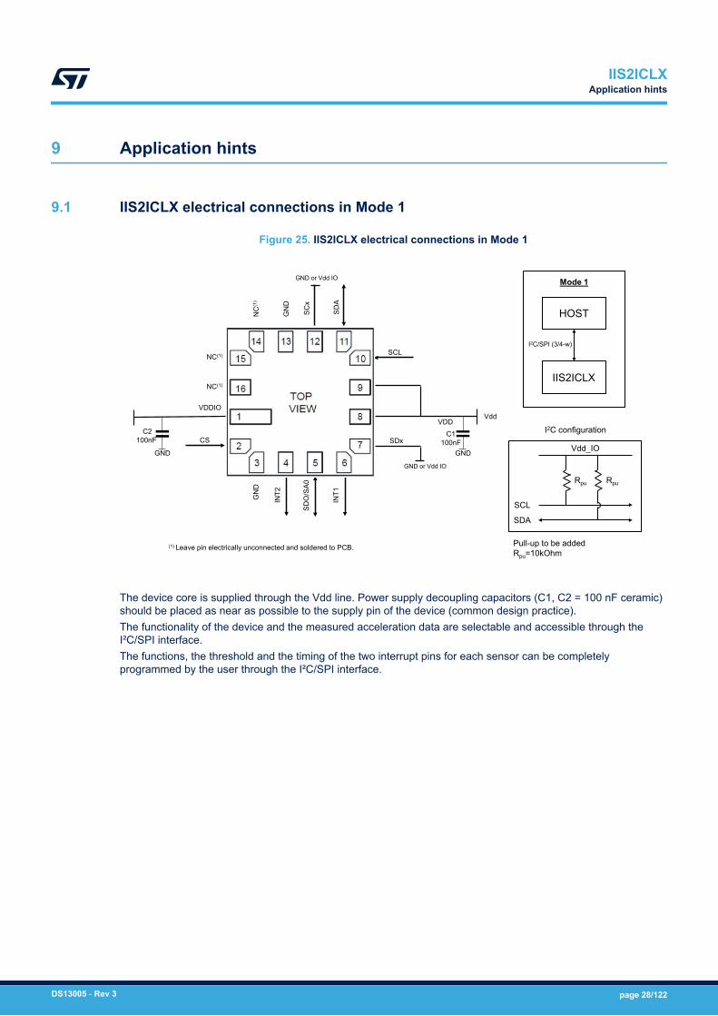
9.1 IIS2ICLX electrical connections in Mode 1
Figure 25. IIS2ICLX electrical connections in Mode 1
VDDIO
C2100nF
GND
CS
GN
D
INT2
SDO
/SA0
INT1
GND or Vdd IO
SDx
VDDVdd
C1100nF
GND
SCL
SDA
GND or Vdd IO
SCx
GN
D
NC
(1)
NC(1)
NC(1)
SCL
SDA
Vdd_IO
Rpu Rpu
Pull-up to be addedRpu=10kOhm
I2C configuration
HOST
IIS2ICLX
I2C/SPI (3/4-w)
Mode 1
(1) Leave pin electrically unconnected and soldered to PCB.
The device core is supplied through the Vdd line. Power supply decoupling capacitors (C1, C2 = 100 nF ceramic)should be placed as near as possible to the supply pin of the device (common design practice).The functionality of the device and the measured acceleration data are selectable and accessible through theI²C/SPI interface.The functions, the threshold and the timing of the two interrupt pins for each sensor can be completelyprogrammed by the user through the I²C/SPI interface.
IIS2ICLXApplication hints
DS13005 - Rev 3 page 28/122
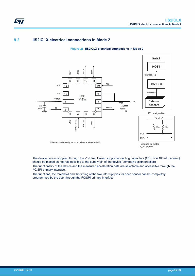
9.2 IIS2ICLX electrical connections in Mode 2
Figure 26. IIS2ICLX electrical connections in Mode 2
VDDIO
C2100nF
GND
CS
GN
D
MD
RD
Y/IN
T2
SDO
/SA0
INT1
MSDA
VDDVdd
C1100nF
GND
SCL
SDA
MSC
L
GN
D
NC(1)
NC(1)
SCL
SDA
Vdd_IO
Rpu Rpu
Pull-up to be addedRpu=10kOhm
I2C configuration
HOST
IIS2ICLX
I2C/SPI (3/4-w)
Mode 2
Master I2C
Externalsensors
NC
(1)
(1) Leave pin electrically unconnected and soldered to PCB.
The device core is supplied through the Vdd line. Power supply decoupling capacitors (C1, C2 = 100 nF ceramic)should be placed as near as possible to the supply pin of the device (common design practice).The functionality of the device and the measured acceleration data are selectable and accessible through theI²C/SPI primary interface.The functions, the threshold and the timing of the two interrupt pins for each sensor can be completelyprogrammed by the user through the I²C/SPI primary interface.
IIS2ICLXIIS2ICLX electrical connections in Mode 2
DS13005 - Rev 3 page 29/122
The procedure to correctly initialize the device is as follows:1. INT1: Leave unconnected or connect with external pull-down during power-on. Pull-up must be avoided on
this pin.2. INT2: Recommend to not connect with external pull-up.3. Properly configure the device:
a. SPI interface: I2C_disable = 1 in CTRL4_C (13h) and DEVICE_CONF = 1 in CTRL9_XL (18h).b. I²C interface: I2C_disable = 0 (default) in CTRL4_C (13h) and DEVICE_CONF = 1 in CTRL9_XL (18h).
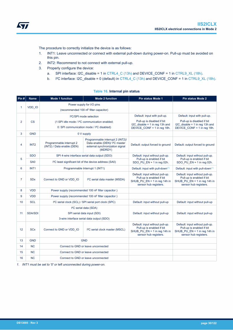
Table 16. Internal pin status
Pin # Name Mode 1 function Mode 2 function Pin status Mode 1 Pin status Mode 2
1 VDD_IOPower supply for I/O pins
(recommended 100 nF filter capacitor)
2 CS
I²C/SPI mode selection
(1:SPI idle mode / I²C communication enabled;
0: SPI communication mode / I²C disabled)
Default: input with pull-up.
Pull-up is disabled if bitI2C_disable = 1 in reg 13h andDEVICE_CONF = 1 in reg 18h.
Default: input with pull-up.
Pull-up is disabled if bitI2C_disable = 1 in reg 13h andDEVICE_CONF = 1 in reg 18h.
3 GND 0 V supply
4 INT2 Programmable interrupt 2(INT2) / Data enable (DEN)
Programmable interrupt 2 (INT2)/Data enable (DEN)/ I²C masterexternal synchronization signal
(MDRDY)
Default: output forced to ground Default: output forced to ground
5SDO SPI 4-wire interface serial data output (SDO) Default: input without pull-up.
Pull-up is enabled if bitSDO_PU_EN = 1 in reg 02h.
Default: input without pull-up.Pull-up is enabled if bit
SDO_PU_EN = 1 in reg 02h.SA0 I²C least significant bit of the device address (SA0)
6 INT1 Programmable Interrupt 1 (INT1) Default: input with pull-down(1) Default: input with pull-down(1)
7 SDx Connect to GND or VDD_IO I²C serial data master (MSDA)
Default: input without pull-up.Pull-up is enabled if bit
SHUB_PU_EN = 1 in reg 14h insensor hub registers.
Default: input without pull-up.Pull-up is enabled if bit
SHUB_PU_EN = 1 in reg 14h insensor hub registers.
8 VDD Power supply (recommended 100 nF filter capacitor )
9 VDD Power supply (recommended 100 nF filter capacitor )
10 SCL I²C serial clock (SCL) / SPI serial port clock (SPC) Default: input without pull-up Default: input without pull-up
11 SDA/SDI
I²C serial data (SDA)
SPI serial data input (SDI)
3-wire interface serial data output (SDO)
Default: input without pull-up Default: input without pull-up
12 SCx Connect to GND or VDD_IO I²C serial clock master (MSCL)
Default: input without pull-up.Pull-up is enabled if bit
SHUB_PU_EN = 1 in reg 14h insensor hub registers.
Default: input without pull-up.Pull-up is enabled if bit
SHUB_PU_EN = 1 in reg 14h insensor hub registers.
13 GND GND
14 NC Connect to GND or leave unconnected
15 NC Connect to GND or leave unconnected
16 NC Connect to GND or leave unconnected
1. INT1 must be set to '0' or left unconnected during power-on.
IIS2ICLXIIS2ICLX electrical connections in Mode 2
DS13005 - Rev 3 page 30/122

10 Register map
The table given below provides a list of the 8/16-bit registers embedded in the device and the correspondingaddresses.
Table 17. Registers address map
Name TypeRegister address
Default CommentHex Binary
FUNC_CFG_ACCESS RW 01 00000001 00000000
PIN_CTRL RW 02 00000010 00111111
RESERVED - 03-06 Reserved
FIFO_CTRL1 RW 07 00000111 00000000
FIFO_CTRL2 RW 08 00001000 00000000
FIFO_CTRL3 RW 09 00001001 00000000
FIFO_CTRL4 RW 0A 00001010 00000000
COUNTER_BDR_REG1 RW 0B 00001011 00000000
COUNTER_BDR_REG2 RW 0C 00001100 00000000
INT1_CTRL RW 0D 00001101 00000000
INT2_CTRL RW 0E 00001110 00000000
WHO_AM_I R 0F 00001111 01101011
CTRL1_XL RW 10 00010000 00000000
RESERVED - 11 00010001 Reserved
CTRL3_C RW 12 00010010 00000100
CTRL4_C RW 13 00010011 00000000
CTRL5_C RW 14 00010100 00000000
CTRL6_C RW 15 00010101 00000000
CTRL7_XL RW 16 00010110 00000000
CTRL8_XL RW 17 00010111 00000000
CTRL9_XL RW 18 00011000 11100000
CTRL10_C RW 19 00011001 00000000
ALL_INT_SRC R 1A 00011010 output
WAKE_UP_SRC R 1B 00011011 output
TAP_SRC R 1C 00011100 output
DEN_SRC R 1D 00011101 output
STATUS_REG R 1E 00011110 output
RESERVED - 1F 00011111 Reserved
OUT_TEMP_L R 20 00100000 output
OUT_TEMP_H R 21 00100001 output
RESERVED - 22-27 00100010 Reserved
OUTX_L_A R 28 00101000 output
OUTX_H_A R 29 00101001 output
IIS2ICLXRegister map
DS13005 - Rev 3 page 31/122

Name TypeRegister address
Default CommentHex Binary
OUTY_L_A R 2A 00101010 output
OUTY_H_A R 2B 00101011 output
RESERVED - 2C-34 Reserved
EMB_FUNC_STATUS_MAINPAGE R 35 00110101 output
FSM_STATUS_A_MAINPAGE R 36 00110110 output
FSM_STATUS_B_MAINPAGE R 37 00110111 output
MLC_STATUS_MAINPAGE R 38 00111000 output
STATUS_MASTER_MAINPAGE R 39 00111001 output
FIFO_STATUS1 R 3A 00111010 output
FIFO_STATUS2 R 3B 00111011 output
RESERVED - 3C-3F Reserved
TIMESTAMP0 R 40 01000000 output
TIMESTAMP1 R 41 01000001 output
TIMESTAMP2 R 42 01000010 output
TIMESTAMP3 R 43 01000011 output
RESERVED - 44-55 Reserved
TAP_CFG0 RW 56 01010110 00000000
TAP_CFG1 RW 57 01010111 Reserved
TAP_CFG2 RW 58 01011000 00000000
RESERVED - 59 01011001 Reserved
INT_DUR2 RW 5A 01011010 00000000
WAKE_UP_THS RW 5B 01011011 00000000
WAKE_UP_DUR RW 5C 01011100 00000000
RESERVED - 5D 01011101 Reserved
MD1_CFG RW 5E 01011110 00000000
MD2_CFG RW 5F 01011111 00000000
RESERVED - 60-62 Reserved
INTERNAL_FREQ_FINE R 63 01100011 output
RESERVED - 64-72 Reserved
X_OFS_USR RW 73 01110011 00000000
Y_OFS_USR RW 74 01110100 00000000
RESERVED - 75-77 Reserved
FIFO_DATA_OUT_TAG R 78 01111000 output
FIFO_DATA_OUT_X_L R 79 01111001 output
FIFO_DATA_OUT_X_H R 7A 01111010 output
FIFO_DATA_OUT_Y_L R 7B 01111011 output
FIFO_DATA_OUT_Y_H R 7C 01111100 output
FIFO_DATA_OUT_Z_L R 7D 01111101 output
FIFO_DATA_OUT_Z_H R 7E 01111110 output
IIS2ICLXRegister map
DS13005 - Rev 3 page 32/122
11 Register description
The device contains a set of registers which are used to control its behavior and to retrieve linear acceleration andtemperature data. The register addresses, made up of 7 bits, are used to identify them and to write the datathrough the serial interface.
11.1 FUNC_CFG_ACCESS (01h)
Enable embedded functions register (r/w)
Table 18. FUNC_CFG_ACCESS register
FUNC_CFG_ACCESS
SHUB_REG_ACCESS 0(1) 0(1) 0(1) 0(1) 0(1) 0(1)
1. This bit must be set to '0' for the correct operation of the device.
Table 19. FUNC_CFG_ACCESS register description
FUNC_CFG_ACCESS Enable access to the embedded functions configuration registers.Default value: 0(1)
SHUB_REG_ACCESS Enable access to the sensor hub (I²C master) registers.Default value: 0(2)
1. Details concerning the embedded functions configuration registers are available in Section 12 Embedded functions registermap and Section 13 Embedded functions register description.
2. Details concerning the sensor hub registers are available in Section 16 Sensor hub register map and Section 17 Sensorhub register description.
11.2 PIN_CTRL (02h)
SDO pin pull-up enable/disable register (r/w)
Table 20. PIN_CTRL register
0(1) SDO_PU_EN 1(2) 1(2) 1(2) 1(2) 1(2) 1(2)
1. This bit must be set to '0' for the correct operation of the device.2. This bit must be set to '1' for the correct operation of the device.
Table 21. PIN_CTRL register description
SDO_PU_ENEnable pull-up on SDO pin. Default value: 0
(0: SDO pin pull-up disconnected (default); 1: SDO pin with pull-up)
IIS2ICLXRegister description
DS13005 - Rev 3 page 33/122
11.3 FIFO_CTRL1 (07h)
FIFO control register 1 (r/w)
Table 22. FIFO_CTRL1 register
WTM7 WTM6 WTM5 WTM4 WTM3 WTM2 WTM1 WTM0
Table 23. FIFO_CTRL1 register description
WTM[7:0]
FIFO watermark threshold, in conjunction with WTM8 in FIFO_CTRL2 (08h)
1 LSB = 1 sensor (6 bytes) + TAG (1 byte) written in FIFO
Watermark flag rises when the number of bytes written in the FIFO is greater than or equal to the threshold level.
11.4 FIFO_CTRL2 (08h)
FIFO control register 2 (r/w)
Table 24. FIFO_CTRL2 register
STOP_ON_WTM 0(1) 0 ODRCHG
_EN 0(1) 0(1) 0(1) WTM8
1. This bit must be set to '0' for the correct operation of the device.
Table 25. FIFO_CTRL2 register
STOP_ON_WTM
Sensing chain FIFO stop values memorization at threshold level
(0: FIFO depth is not limited (default);
1: FIFO depth is limited to the threshold level, defined in FIFO_CTRL1 (07h) and FIFO_CTRL2 (08h)
ODRCHG_EN Enables ODR CHANGE virtual sensor to be batched in FIFO
WTM8
FIFO watermark threshold, in conjunction with WTM[7:0] in FIFO_CTRL1 (07h)
1 LSB = 1 sensor (6 bytes) + TAG (1 byte) written in FIFO
Watermark flag rises when the number of bytes written in FIFO is greater than or equal to the thresholdlevel.
IIS2ICLXFIFO_CTRL1 (07h)
DS13005 - Rev 3 page 34/122

11.5 FIFO_CTRL3 (09h)
FIFO control register 3 (r/w)
Table 26. FIFO_CTRL3 register
0(1) 0(1) 0(1) 0(1) BDR_XL_3 BDR_XL_2 BDR_XL_1 BDR_XL_0
1. This bit must be set to '0' for the correct operation of the device.
Table 27. FIFO_CTRL3 register description
BDR_XL_[3:0]
Selects Batch Data Rate (write frequency in FIFO) for accelerometer data.
(0000: Accelerometer not batched in FIFO (default);
0001: 12.5 Hz;
0010: 26 Hz;
0011: 52 Hz;
0100: 104 Hz;
0101: 208 Hz;
0110: 417 Hz;
0111: 833 Hz;
1000: not allowed;
1001: not allowed;
1010: not allowed;
1011: 1.6 Hz;
1100-1111: not allowed)
IIS2ICLXFIFO_CTRL3 (09h)
DS13005 - Rev 3 page 35/122
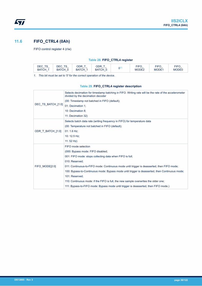
11.6 FIFO_CTRL4 (0Ah)
FIFO control register 4 (r/w)
Table 28. FIFO_CTRL4 register
DEC_TS_BATCH_1
DEC_TS_BATCH_0
ODR_T_BATCH_1
ODR_T_BATCH_0 0(1) FIFO_
MODE2FIFO_
MODE1FIFO_
MODE0
1. This bit must be set to '0' for the correct operation of the device.
Table 29. FIFO_CTRL4 register description
DEC_TS_BATCH_[1:0]
Selects decimation for timestamp batching in FIFO. Writing rate will be the rate of the accelerometerdivided by the decimation decoder
(00: Timestamp not batched in FIFO (default);
01: Decimation 1;
10: Decimation 8;
11: Decimation 32)
ODR_T_BATCH_[1:0]
Selects batch data rate (writing frequency in FIFO) for temperature data
(00: Temperature not batched in FIFO (default);
01: 1.6 Hz;
10: 12.5 Hz;
11: 52 Hz)
FIFO_MODE[2:0]
FIFO mode selection
(000: Bypass mode: FIFO disabled;
001: FIFO mode: stops collecting data when FIFO is full;
010: Reserved;
011: Continuous-to-FIFO mode: Continuous mode until trigger is deasserted, then FIFO mode;
100: Bypass-to-Continuous mode: Bypass mode until trigger is deasserted, then Continuous mode;
101: Reserved;
110: Continuous mode: if the FIFO is full, the new sample overwrites the older one;
111: Bypass-to-FIFO mode: Bypass mode until trigger is deasserted, then FIFO mode.)
IIS2ICLXFIFO_CTRL4 (0Ah)
DS13005 - Rev 3 page 36/122
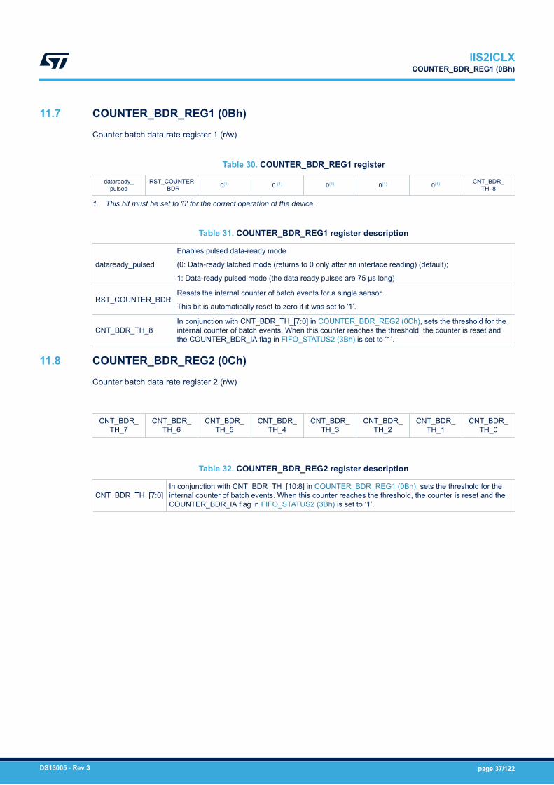
11.7 COUNTER_BDR_REG1 (0Bh)
Counter batch data rate register 1 (r/w)
Table 30. COUNTER_BDR_REG1 register
dataready_pulsed
RST_COUNTER_BDR 0(1) 0 (1) 0(1) 0(1) 0(1) CNT_BDR_
TH_8
1. This bit must be set to '0' for the correct operation of the device.
Table 31. COUNTER_BDR_REG1 register description
dataready_pulsed
Enables pulsed data-ready mode
(0: Data-ready latched mode (returns to 0 only after an interface reading) (default);
1: Data-ready pulsed mode (the data ready pulses are 75 µs long)
RST_COUNTER_BDRResets the internal counter of batch events for a single sensor.
This bit is automatically reset to zero if it was set to ‘1’.
CNT_BDR_TH_8In conjunction with CNT_BDR_TH_[7:0] in COUNTER_BDR_REG2 (0Ch), sets the threshold for theinternal counter of batch events. When this counter reaches the threshold, the counter is reset andthe COUNTER_BDR_IA flag in FIFO_STATUS2 (3Bh) is set to ‘1’.
11.8 COUNTER_BDR_REG2 (0Ch)
Counter batch data rate register 2 (r/w)
CNT_BDR_TH_7
CNT_BDR_TH_6
CNT_BDR_TH_5
CNT_BDR_TH_4
CNT_BDR_TH_3
CNT_BDR_TH_2
CNT_BDR_TH_1
CNT_BDR_TH_0
Table 32. COUNTER_BDR_REG2 register description
CNT_BDR_TH_[7:0]In conjunction with CNT_BDR_TH_[10:8] in COUNTER_BDR_REG1 (0Bh), sets the threshold for theinternal counter of batch events. When this counter reaches the threshold, the counter is reset and theCOUNTER_BDR_IA flag in FIFO_STATUS2 (3Bh) is set to ‘1’.
IIS2ICLXCOUNTER_BDR_REG1 (0Bh)
DS13005 - Rev 3 page 37/122
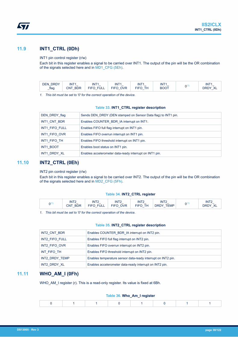
11.9 INT1_CTRL (0Dh)
INT1 pin control register (r/w)Each bit in this register enables a signal to be carried over INT1. The output of the pin will be the OR combinationof the signals selected here and in MD1_CFG (5Eh).
DEN_DRDY_flag
INT1_CNT_BDR
INT1_FIFO_FULL
INT1_FIFO_OVR
INT1_FIFO_TH
INT1_BOOT 0(1) INT1_
DRDY_XL
1. This bit must be set to '0' for the correct operation of the device.
Table 33. INT1_CTRL register description
DEN_DRDY_flag Sends DEN_DRDY (DEN stamped on Sensor Data flag) to INT1 pin.
INT1_CNT_BDR Enables COUNTER_BDR_IA interrupt on INT1.
INT1_FIFO_FULL Enables FIFO full flag interrupt on INT1 pin.
INT1_FIFO_OVR Enables FIFO overrun interrupt on INT1 pin.
INT1_FIFO_TH Enables FIFO threshold interrupt on INT1 pin.
INT1_BOOT Enables boot status on INT1 pin.
INT1_DRDY_XL Enables accelerometer data-ready interrupt on INT1 pin.
11.10 INT2_CTRL (0Eh)
INT2 pin control register (r/w)Each bit in this register enables a signal to be carried over INT2. The output of the pin will be the OR combinationof the signals selected here and in MD2_CFG (5Fh).
Table 34. INT2_CTRL register
0(1) INT2_CNT_BDR
INT2_FIFO_FULL
INT2_FIFO_OVR
INT2_FIFO_TH
INT2_DRDY_TEMP 0(1) INT2_
DRDY_XL
1. This bit must be set to '0' for the correct operation of the device.
Table 35. INT2_CTRL register description
INT2_CNT_BDR Enables COUNTER_BDR_IA interrupt on INT2 pin.
INT2_FIFO_FULL Enables FIFO full flag interrupt on INT2 pin.
INT2_FIFO_OVR Enables FIFO overrun interrupt on INT2 pin.
INT_FIFO_TH Enables FIFO threshold interrupt on INT2 pin.
INT2_DRDY_TEMP Enables temperature sensor data-ready interrupt on INT2 pin.
INT2_DRDY_XL Enables accelerometer data-ready interrupt on INT2 pin.
11.11 WHO_AM_I (0Fh)
WHO_AM_I register (r). This is a read-only register. Its value is fixed at 6Bh.
Table 36. Who_Am_I register
0 1 1 0 1 0 1 1
IIS2ICLXINT1_CTRL (0Dh)
DS13005 - Rev 3 page 38/122

11.12 CTRL1_XL (10h)
Accelerometer control register 1 (r/w)
ODR_XL3 ODR_XL2 ODR_XL1 ODR_XL0 FS1_XL FS0_XL LPF2_XL_EN 0(1)
1. This bit must be set to '0' for the correct operation of the device.
Table 37. CTRL1_XL register description
ODR_XL[3:0] Accelerometer ODR selection (see Table 38)
FS[1:0]_XL Accelerometer full-scale selection (see Table 39)
LPF2_XL_EN
Accelerometer high-resolution selection
(0: output from first stage digital filtering selected (default);
1: output from LPF2 second filtering stage selected)
Table 38. Accelerometer ODR register setting
ODR_XL3 ODR_XL2 ODR_XL1 ODR_XL0 ODR selection [Hz]
0 0 0 0 Power-down
1 0 1 1 12.5 Hz
0 0 0 1 12.5 Hz
0 0 1 0 26 Hz
0 0 1 1 52 Hz
0 1 0 0 104 Hz
0 1 0 1 208 Hz
0 1 1 0 416 Hz
0 1 1 1 833 Hz
1 0 0 0
RESERVED1 0 0 1
1 0 1 0
1 1 x x Not allowed
Table 39. Accelerometer full-scale selection
FS[1:0]_XL XL_FS
00 ±0.5 g
01 ±3 g
10 ±1 g
11 ±2 g
IIS2ICLXCTRL1_XL (10h)
DS13005 - Rev 3 page 39/122
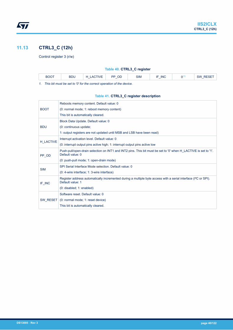
11.13 CTRL3_C (12h)
Control register 3 (r/w)
Table 40. CTRL3_C register
BOOT BDU H_LACTIVE PP_OD SIM IF_INC 0(1) SW_RESET
1. This bit must be set to '0' for the correct operation of the device.
Table 41. CTRL3_C register description
BOOT
Reboots memory content. Default value: 0
(0: normal mode; 1: reboot memory content)
This bit is automatically cleared.
BDU
Block Data Update. Default value: 0
(0: continuous update;
1: output registers are not updated until MSB and LSB have been read)
H_LACTIVEInterrupt activation level. Default value: 0
(0: interrupt output pins active high; 1: interrupt output pins active low
PP_ODPush-pull/open-drain selection on INT1 and INT2 pins. This bit must be set to '0' when H_LACTIVE is set to '1'.Default value: 0
(0: push-pull mode; 1: open-drain mode)
SIMSPI Serial Interface Mode selection. Default value: 0
(0: 4-wire interface; 1: 3-wire interface)
IF_INCRegister address automatically incremented during a multiple byte access with a serial interface (I²C or SPI).Default value: 1
(0: disabled; 1: enabled)
SW_RESET
Software reset. Default value: 0
(0: normal mode; 1: reset device)
This bit is automatically cleared.
IIS2ICLXCTRL3_C (12h)
DS13005 - Rev 3 page 40/122
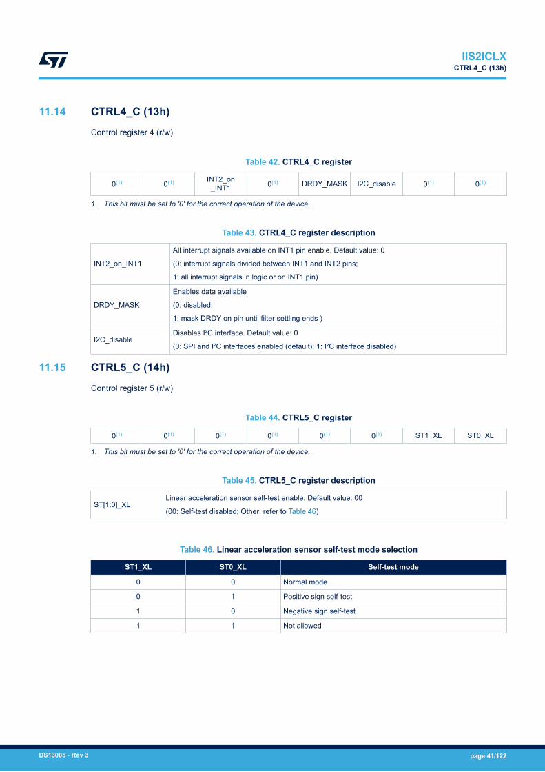
11.14 CTRL4_C (13h)
Control register 4 (r/w)
Table 42. CTRL4_C register
0(1) 0(1) INT2_on_INT1 0(1) DRDY_MASK I2C_disable 0(1) 0(1)
1. This bit must be set to '0' for the correct operation of the device.
Table 43. CTRL4_C register description
INT2_on_INT1
All interrupt signals available on INT1 pin enable. Default value: 0
(0: interrupt signals divided between INT1 and INT2 pins;
1: all interrupt signals in logic or on INT1 pin)
DRDY_MASK
Enables data available
(0: disabled;
1: mask DRDY on pin until filter settling ends )
I2C_disableDisables I²C interface. Default value: 0
(0: SPI and I²C interfaces enabled (default); 1: I²C interface disabled)
11.15 CTRL5_C (14h)
Control register 5 (r/w)
Table 44. CTRL5_C register
0(1) 0(1) 0(1) 0(1) 0(1) 0(1) ST1_XL ST0_XL
1. This bit must be set to '0' for the correct operation of the device.
Table 45. CTRL5_C register description
ST[1:0]_XLLinear acceleration sensor self-test enable. Default value: 00
(00: Self-test disabled; Other: refer to Table 46)
Table 46. Linear acceleration sensor self-test mode selection
ST1_XL ST0_XL Self-test mode
0 0 Normal mode
0 1 Positive sign self-test
1 0 Negative sign self-test
1 1 Not allowed
IIS2ICLXCTRL4_C (13h)
DS13005 - Rev 3 page 41/122
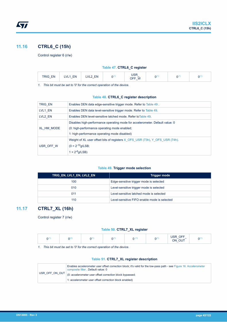
11.16 CTRL6_C (15h)
Control register 6 (r/w)
Table 47. CTRL6_C register
TRIG_EN LVL1_EN LVL2_EN 0(1) USR_OFF_W 0(1) 0(1) 0(1)
1. This bit must be set to '0' for the correct operation of the device.
Table 48. CTRL6_C register description
TRIG_EN Enables DEN data edge-sensitive trigger mode. Refer to Table 49 .
LVL1_EN Enables DEN data level-sensitive trigger mode. Refer to Table 49.
LVL2_EN Enables DEN level-sensitive latched mode. Refer toTable 49.
XL_HM_MODE
Disables high-performance operating mode for accelerometer. Default value: 0
(0: high-performance operating mode enabled;
1: high-performance operating mode disabled)
USR_OFF_W
Weight of XL user offset bits of registers X_OFS_USR (73h), Y_OFS_USR (74h).
(0 = 2-10g/LSB;
1 = 2-6g/LSB)
Table 49. Trigger mode selection
TRIG_EN, LVL1_EN, LVL2_EN Trigger mode
100 Edge-sensitive trigger mode is selected
010 Level-sensitive trigger mode is selected
011 Level-sensitive latched mode is selected
110 Level-sensitive FIFO enable mode is selected
11.17 CTRL7_XL (16h)
Control register 7 (r/w)
Table 50. CTRL7_XL register
0(1) 0(1) 0(1) 0(1) 0 (1) 0(1) USR_OFF_ON_OUT 0(1)
1. This bit must be set to '0' for the correct operation of the device.
Table 51. CTRL7_XL register description
USR_OFF_ON_OUT
Enables accelerometer user offset correction block; it's valid for the low-pass path - see Figure 16. Accelerometercomposite filter . Default value: 0
(0: accelerometer user offset correction block bypassed;
1: accelerometer user offset correction block enabled)
IIS2ICLXCTRL6_C (15h)
DS13005 - Rev 3 page 42/122
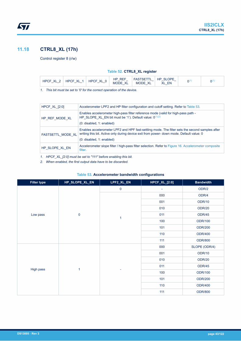
11.18 CTRL8_XL (17h)
Control register 8 (r/w)
Table 52. CTRL8_XL register
HPCF_XL_2 HPCF_XL_1 HPCF_XL_0 HP_REF_MODE_XL
FASTSETTL_MODE_XL
HP_SLOPE_XL_EN 0(1) 0(1)
1. This bit must be set to '0' for the correct operation of the device.
HPCF_XL_[2:0] Accelerometer LPF2 and HP filter configuration and cutoff setting. Refer to Table 53.
HP_REF_MODE_XLEnables accelerometer high-pass filter reference mode (valid for high-pass path -HP_SLOPE_XL_EN bit must be ‘1’). Default value: 0(1)(2)
(0: disabled, 1: enabled)
FASTSETTL_MODE_XLEnables accelerometer LPF2 and HPF fast-settling mode. The filter sets the second samples afterwriting this bit. Active only during device exit from power- down mode. Default value: 0
(0: disabled, 1: enabled)
HP_SLOPE_XL_EN Accelerometer slope filter / high-pass filter selection. Refer to Figure 16. Accelerometer compositefilter.
1. HPCF_XL_[2:0] must be set to "111" before enabling this bit.2. When enabled, the first output data have to be discarded.
Table 53. Accelerometer bandwidth configurations
Filter type HP_SLOPE_XL_EN LPF2_XL_EN HPCF_XL_[2:0] Bandwidth
Low pass 0
0 - ODR/2
1
000 ODR/4
001 ODR/10
010 ODR/20
011 ODR/45
100 ODR/100
101 ODR/200
110 ODR/400
111 ODR/800
High pass 1 -
000 SLOPE (ODR/4)
001 ODR/10
010 ODR/20
011 ODR/45
100 ODR/100
101 ODR/200
110 ODR/400
111 ODR/800
IIS2ICLXCTRL8_XL (17h)
DS13005 - Rev 3 page 43/122
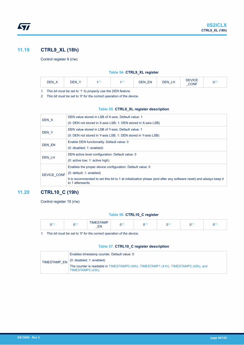
11.19 CTRL9_XL (18h)
Control register 9 (r/w)
Table 54. CTRL9_XL register
DEN_X DEN_Y 1(1) 1(1) DEN_EN DEN_LH DEVICE_CONF 0(2)
1. This bit must be set to ‘1’ to properly use the DEN feature.2. This bit must be set to '0' for the correct operation of the device.
Table 55. CTRL9_XL register description
DEN_XDEN value stored in LSB of X-axis. Default value: 1
(0: DEN not stored in X-axis LSB; 1: DEN stored in X-axis LSB)
DEN_YDEN value stored in LSB of Y-axis. Default value: 1
(0: DEN not stored in Y-axis LSB; 1: DEN stored in Y-axis LSB)
DEN_ENEnable DEN functionality. Default value: 0
(0: disabled; 1: enabled)
DEN_LHDEN active level configuration. Default value: 0
(0: active low; 1: active high)
DEVICE_CONF
Enables the proper device configuration. Default value: 0
(0: default; 1: enabled)
It is recommended to set this bit to 1 at initialization phase (and after any software reset) and always keep itto 1 afterwards.
11.20 CTRL10_C (19h)
Control register 10 (r/w)
Table 56. CTRL10_C register
0(1) 0(1) TIMESTAMP_EN 0(1) 0(1) 0(1) 0(1) 0(1)
1. This bit must be set to '0' for the correct operation of the device.
Table 57. CTRL10_C register description
TIMESTAMP_EN
Enables timestamp counter. Default value: 0
(0: disabled; 1: enabled)
The counter is readable in TIMESTAMP0 (40h), TIMESTAMP1 (41h), TIMESTAMP2 (42h), andTIMESTAMP3 (43h).
IIS2ICLXCTRL9_XL (18h)
DS13005 - Rev 3 page 44/122

11.21 ALL_INT_SRC (1Ah)
Source register for all interrupts (r)
Table 58. ALL_INT_SRC register
TIMESTAMP_ENDCOUNT 0 SLEEP_
CHANGE 0 DOUBLE_TAP
SINGLE_TAP WU_IA 0
Table 59. ALL_INT_SRC register description
TIMESTAMP_ENDCOUNT Alerts timestamp overflow within 6.4 ms
SLEEP_CHANGEDetects change event in stationary/motion status. Default value: 0
(0: change status not detected; 1: change status detected)
DOUBLE_TAP Double-tap event status. Default value: 0(0:event not detected, 1: event detected)
SINGLE_TAP Single-tap event status. Default value: 0(0:event not detected, 1: event detected)
WU_IAWake-up event status. Default value: 0
(0: event not detected, 1: event detected)
11.22 WAKE_UP_SRC (1Bh)
Wake-up interrupt source register (r)
Table 60. WAKE_UP_SRC register
0 SLEEP_CHANGE_IA 0 SLEEP_
STATE WU_IA X_WU Y_WU 0
Table 61. WAKE_UP_SRC register description
SLEEP_CHANGE_IADetects change event in stationary/motion status. Default value: 0
(0: change status not detected; 1: change status detected)
SLEEP_STATESleep status bit. Default value: 0
(0: sleep event not detected; 1: sleep event detected)
WU_IAWakeup event detection status. Default value: 0
(0: wakeup event not detected; 1: wakeup event detected.)
X_WUWakeup event detection status on X-axis. Default value: 0
(0: wakeup event on X-axis not detected; 1: wakeup event on X-axis detected)
Y_WUWakeup event detection status on Y-axis. Default value: 0
(0: wakeup event on Y-axis not detected; 1: wakeup event on Y-axis detected)
IIS2ICLXALL_INT_SRC (1Ah)
DS13005 - Rev 3 page 45/122
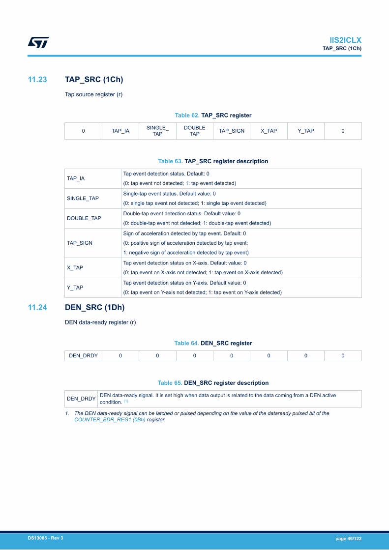
11.23 TAP_SRC (1Ch)
Tap source register (r)
Table 62. TAP_SRC register
0 TAP_IA SINGLE_TAP
DOUBLETAP TAP_SIGN X_TAP Y_TAP 0
Table 63. TAP_SRC register description
TAP_IATap event detection status. Default: 0
(0: tap event not detected; 1: tap event detected)
SINGLE_TAPSingle-tap event status. Default value: 0
(0: single tap event not detected; 1: single tap event detected)
DOUBLE_TAPDouble-tap event detection status. Default value: 0
(0: double-tap event not detected; 1: double-tap event detected)
TAP_SIGN
Sign of acceleration detected by tap event. Default: 0
(0: positive sign of acceleration detected by tap event;
1: negative sign of acceleration detected by tap event)
X_TAPTap event detection status on X-axis. Default value: 0
(0: tap event on X-axis not detected; 1: tap event on X-axis detected)
Y_TAPTap event detection status on Y-axis. Default value: 0
(0: tap event on Y-axis not detected; 1: tap event on Y-axis detected)
11.24 DEN_SRC (1Dh)
DEN data-ready register (r)
Table 64. DEN_SRC register
DEN_DRDY 0 0 0 0 0 0 0
Table 65. DEN_SRC register description
DEN_DRDY DEN data-ready signal. It is set high when data output is related to the data coming from a DEN activecondition. (1)
1. The DEN data-ready signal can be latched or pulsed depending on the value of the dataready pulsed bit of theCOUNTER_BDR_REG1 (0Bh) register.
IIS2ICLXTAP_SRC (1Ch)
DS13005 - Rev 3 page 46/122
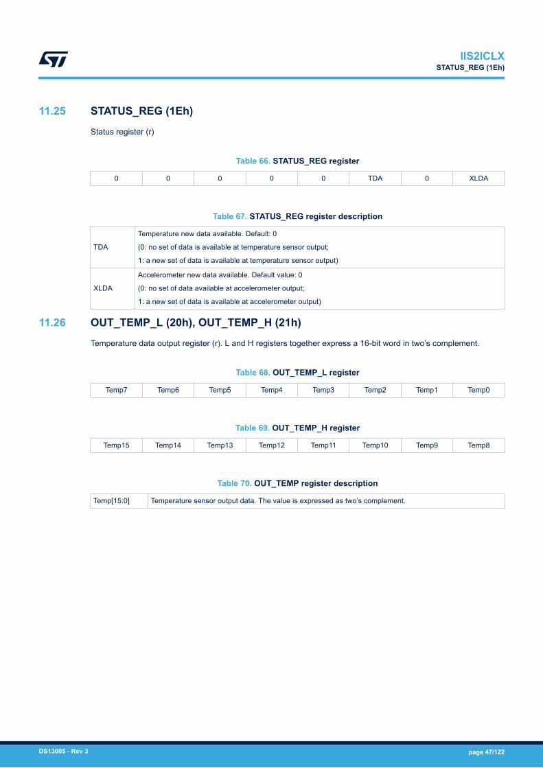
11.25 STATUS_REG (1Eh)
Status register (r)
Table 66. STATUS_REG register
0 0 0 0 0 TDA 0 XLDA
Table 67. STATUS_REG register description
TDA
Temperature new data available. Default: 0
(0: no set of data is available at temperature sensor output;
1: a new set of data is available at temperature sensor output)
XLDA
Accelerometer new data available. Default value: 0
(0: no set of data available at accelerometer output;
1: a new set of data is available at accelerometer output)
11.26 OUT_TEMP_L (20h), OUT_TEMP_H (21h)
Temperature data output register (r). L and H registers together express a 16-bit word in two’s complement.
Table 68. OUT_TEMP_L register
Temp7 Temp6 Temp5 Temp4 Temp3 Temp2 Temp1 Temp0
Table 69. OUT_TEMP_H register
Temp15 Temp14 Temp13 Temp12 Temp11 Temp10 Temp9 Temp8
Table 70. OUT_TEMP register description
Temp[15:0] Temperature sensor output data. The value is expressed as two’s complement.
IIS2ICLXSTATUS_REG (1Eh)
DS13005 - Rev 3 page 47/122

11.27 OUTX_L_A (28h) and OUTX_H_A (29h)
Linear acceleration sensor X-axis output register (r). The value is expressed as a 16-bit word in two’scomplement.
Table 71. OUTX_L_A register
D7 D6 D5 D4 D3 D2 D1 D0
Table 72. OUTX_H_A register
D15 D14 D13 D12 D11 D10 D9 D8
Table 73. OUTX_H_A register description
D[15:0] X-axis linear acceleration value. D[15:0] expressed in two’s complement.
11.28 OUTY_L_A (2Ah) and OUTY_H_A (2Bh)
Linear acceleration sensor Y-axis output register (r). The value is expressed as a 16-bit word in two’scomplement.
Table 74. OUTY_L_A register
D7 D6 D5 D4 D3 D2 D1 D0
Table 75. OUTY_H_A register
D15 D14 D13 D12 D11 D10 D9 D8
Table 76. OUTY_H_A register description
D[15:0] Y-axis linear acceleration value. D[15:0] expressed in two’s complement.
11.29 EMB_FUNC_STATUS_MAINPAGE (35h)
Embedded function status register (r)
Table 77. EMB_FUNC_STATUS_MAINPAGE register
IS_FSM_LC 0 0 0 0 0 0 0
Table 78. EMB_FUNC_STATUS_MAINPAGE register description
IS_FSM_LC Interrupt status bit for FSM long counter timeout interrupt event.(1: interrupt detected; 0: no interrupt)
IIS2ICLXOUTX_L_A (28h) and OUTX_H_A (29h)
DS13005 - Rev 3 page 48/122
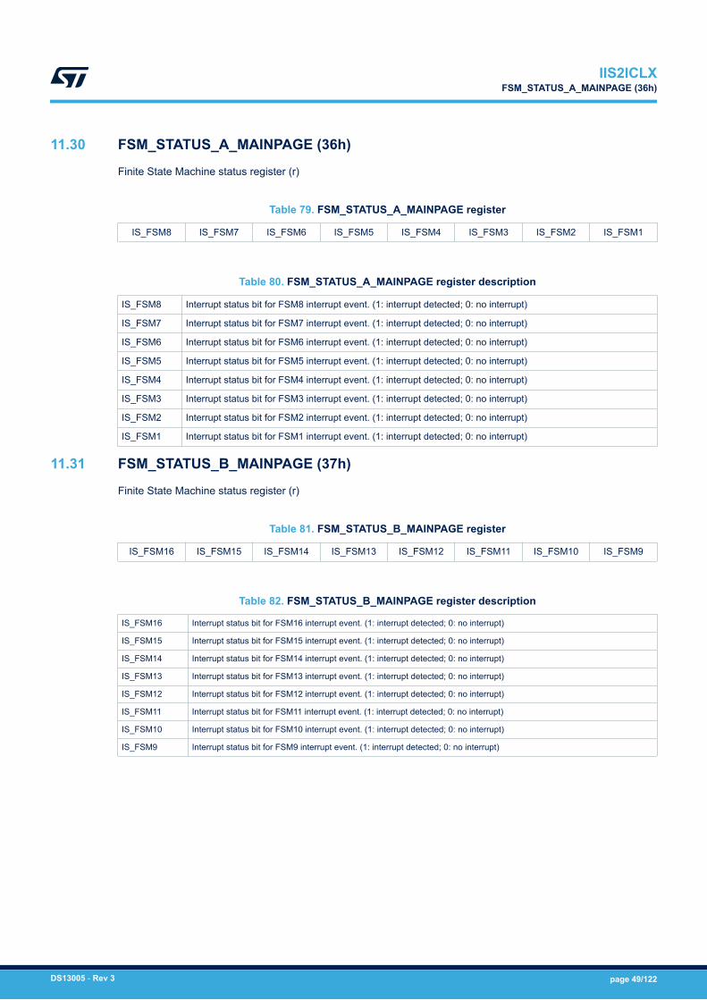
11.30 FSM_STATUS_A_MAINPAGE (36h)
Finite State Machine status register (r)
Table 79. FSM_STATUS_A_MAINPAGE register
IS_FSM8 IS_FSM7 IS_FSM6 IS_FSM5 IS_FSM4 IS_FSM3 IS_FSM2 IS_FSM1
Table 80. FSM_STATUS_A_MAINPAGE register description
IS_FSM8 Interrupt status bit for FSM8 interrupt event. (1: interrupt detected; 0: no interrupt)
IS_FSM7 Interrupt status bit for FSM7 interrupt event. (1: interrupt detected; 0: no interrupt)
IS_FSM6 Interrupt status bit for FSM6 interrupt event. (1: interrupt detected; 0: no interrupt)
IS_FSM5 Interrupt status bit for FSM5 interrupt event. (1: interrupt detected; 0: no interrupt)
IS_FSM4 Interrupt status bit for FSM4 interrupt event. (1: interrupt detected; 0: no interrupt)
IS_FSM3 Interrupt status bit for FSM3 interrupt event. (1: interrupt detected; 0: no interrupt)
IS_FSM2 Interrupt status bit for FSM2 interrupt event. (1: interrupt detected; 0: no interrupt)
IS_FSM1 Interrupt status bit for FSM1 interrupt event. (1: interrupt detected; 0: no interrupt)
11.31 FSM_STATUS_B_MAINPAGE (37h)
Finite State Machine status register (r)
Table 81. FSM_STATUS_B_MAINPAGE register
IS_FSM16 IS_FSM15 IS_FSM14 IS_FSM13 IS_FSM12 IS_FSM11 IS_FSM10 IS_FSM9
Table 82. FSM_STATUS_B_MAINPAGE register description
IS_FSM16 Interrupt status bit for FSM16 interrupt event. (1: interrupt detected; 0: no interrupt)
IS_FSM15 Interrupt status bit for FSM15 interrupt event. (1: interrupt detected; 0: no interrupt)
IS_FSM14 Interrupt status bit for FSM14 interrupt event. (1: interrupt detected; 0: no interrupt)
IS_FSM13 Interrupt status bit for FSM13 interrupt event. (1: interrupt detected; 0: no interrupt)
IS_FSM12 Interrupt status bit for FSM12 interrupt event. (1: interrupt detected; 0: no interrupt)
IS_FSM11 Interrupt status bit for FSM11 interrupt event. (1: interrupt detected; 0: no interrupt)
IS_FSM10 Interrupt status bit for FSM10 interrupt event. (1: interrupt detected; 0: no interrupt)
IS_FSM9 Interrupt status bit for FSM9 interrupt event. (1: interrupt detected; 0: no interrupt)
IIS2ICLXFSM_STATUS_A_MAINPAGE (36h)
DS13005 - Rev 3 page 49/122

11.32 MLC_STATUS_MAINPAGE (38h)
Machine Learning Core status register (r)
Table 83. MLC_STATUS_MAINPAGE register
IS_MLC8 IS_MLC7 IS_MLC6 IS_MLC5 IS_MLC4 IS_MLC3 IS_MLC2 IS_MLC1
Table 84. MLC_STATUS_MAINPAGE register description
IS_MLC8 Interrupt status bit for MLC8 interrupt event. (1: interrupt detected; 0: no interrupt)
IS_MLC7 Interrupt status bit for MLC7 interrupt event. (1: interrupt detected; 0: no interrupt)
IS_MLC6 Interrupt status bit for MLC6 interrupt event. (1: interrupt detected; 0: no interrupt)
IS_MLC5 Interrupt status bit for MLC5 interrupt event. (1: interrupt detected; 0: no interrupt)
IS_MLC4 Interrupt status bit for MLC4 interrupt event. (1: interrupt detected; 0: no interrupt)
IS_MLC3 Interrupt status bit for MLC3 interrupt event. (1: interrupt detected; 0: no interrupt)
IS_MLC2 Interrupt status bit for MLC2 interrupt event. (1: interrupt detected; 0: no interrupt)
IS_MLC1 Interrupt status bit for MLC1 interrupt event. (1: interrupt detected; 0: no interrupt)
11.33 STATUS_MASTER_MAINPAGE (39h)
Sensor hub source register (r)
Table 85. STATUS_MASTER_MAINPAGE register
WR_ONCE_DONE
SLAVE3_NACK
SLAVE2_NACK
SLAVE1_NACK
SLAVE0_NACK 0 0 SENS_HUB_
ENDOP
Table 86. STATUS_MASTER_MAINPAGE register description
WR_ONCE_DONE When the bit WRITE_ONCE in MASTER_CONFIG (14h) is configured as 1, this bit is set to 1 when thewrite operation on slave 0 has been performed and completed. Default value: 0
SLAVE3_NACK This bit is set to 1 if Not acknowledge occurs on slave 3 communication. Default value: 0
SLAVE2_NACK This bit is set to 1 if Not acknowledge occurs on slave 2 communication. Default value: 0
SLAVE1_NACK This bit is set to 1 if Not acknowledge occurs on slave 1 communication. Default value: 0
SLAVE0_NACK This bit is set to 1 if Not acknowledge occurs on slave 0 communication. Default value: 0
SENS_HUB_ENDOP
Sensor hub communication status. Default value: 0
(0: sensor hub communication not concluded;
1: sensor hub communication concluded)
IIS2ICLXMLC_STATUS_MAINPAGE (38h)
DS13005 - Rev 3 page 50/122
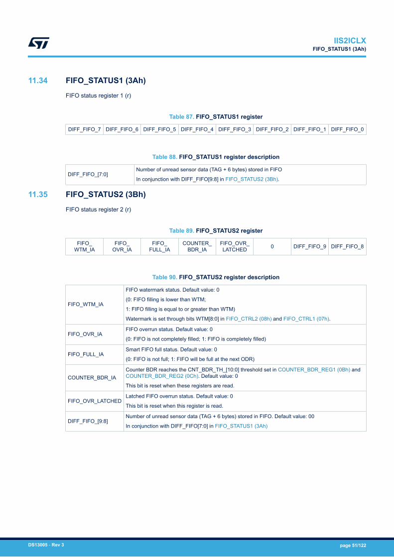
11.34 FIFO_STATUS1 (3Ah)
FIFO status register 1 (r)
Table 87. FIFO_STATUS1 register
DIFF_FIFO_7 DIFF_FIFO_6 DIFF_FIFO_5 DIFF_FIFO_4 DIFF_FIFO_3 DIFF_FIFO_2 DIFF_FIFO_1 DIFF_FIFO_0
Table 88. FIFO_STATUS1 register description
DIFF_FIFO_[7:0]Number of unread sensor data (TAG + 6 bytes) stored in FIFO
In conjunction with DIFF_FIFO[9:8] in FIFO_STATUS2 (3Bh).
11.35 FIFO_STATUS2 (3Bh)
FIFO status register 2 (r)
Table 89. FIFO_STATUS2 register
FIFO_WTM_IA
FIFO_OVR_IA
FIFO_FULL_IA
COUNTER_BDR_IA
FIFO_OVR_LATCHED 0 DIFF_FIFO_9 DIFF_FIFO_8
Table 90. FIFO_STATUS2 register description
FIFO_WTM_IA
FIFO watermark status. Default value: 0
(0: FIFO filling is lower than WTM;
1: FIFO filling is equal to or greater than WTM)
Watermark is set through bits WTM[8:0] in FIFO_CTRL2 (08h) and FIFO_CTRL1 (07h).
FIFO_OVR_IAFIFO overrun status. Default value: 0
(0: FIFO is not completely filled; 1: FIFO is completely filled)
FIFO_FULL_IASmart FIFO full status. Default value: 0
(0: FIFO is not full; 1: FIFO will be full at the next ODR)
COUNTER_BDR_IACounter BDR reaches the CNT_BDR_TH_[10:0] threshold set in COUNTER_BDR_REG1 (0Bh) andCOUNTER_BDR_REG2 (0Ch). Default value: 0
This bit is reset when these registers are read.
FIFO_OVR_LATCHEDLatched FIFO overrun status. Default value: 0
This bit is reset when this register is read.
DIFF_FIFO_[9:8]Number of unread sensor data (TAG + 6 bytes) stored in FIFO. Default value: 00
In conjunction with DIFF_FIFO[7:0] in FIFO_STATUS1 (3Ah)
IIS2ICLXFIFO_STATUS1 (3Ah)
DS13005 - Rev 3 page 51/122
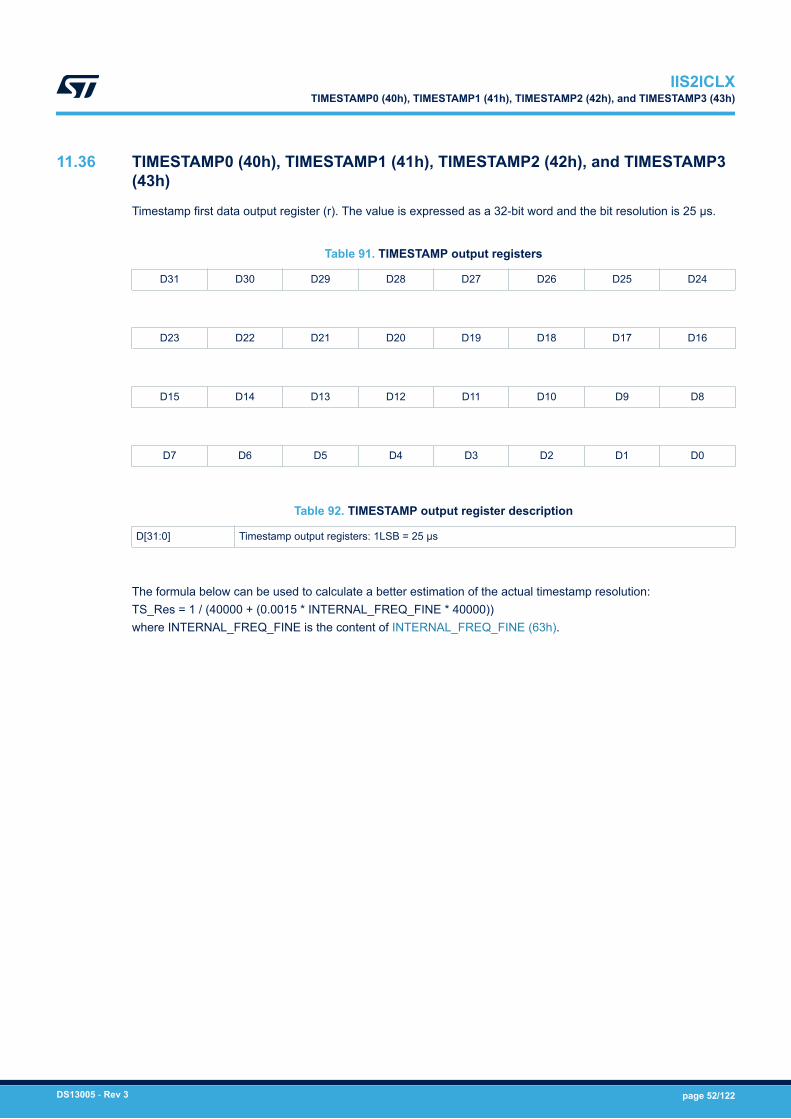
11.36 TIMESTAMP0 (40h), TIMESTAMP1 (41h), TIMESTAMP2 (42h), and TIMESTAMP3(43h)
Timestamp first data output register (r). The value is expressed as a 32-bit word and the bit resolution is 25 µs.
Table 91. TIMESTAMP output registers
D31 D30 D29 D28 D27 D26 D25 D24
D23 D22 D21 D20 D19 D18 D17 D16
D15 D14 D13 D12 D11 D10 D9 D8
D7 D6 D5 D4 D3 D2 D1 D0
Table 92. TIMESTAMP output register description
D[31:0] Timestamp output registers: 1LSB = 25 µs
The formula below can be used to calculate a better estimation of the actual timestamp resolution:TS_Res = 1 / (40000 + (0.0015 * INTERNAL_FREQ_FINE * 40000))where INTERNAL_FREQ_FINE is the content of INTERNAL_FREQ_FINE (63h).
IIS2ICLXTIMESTAMP0 (40h), TIMESTAMP1 (41h), TIMESTAMP2 (42h), and TIMESTAMP3 (43h)
DS13005 - Rev 3 page 52/122
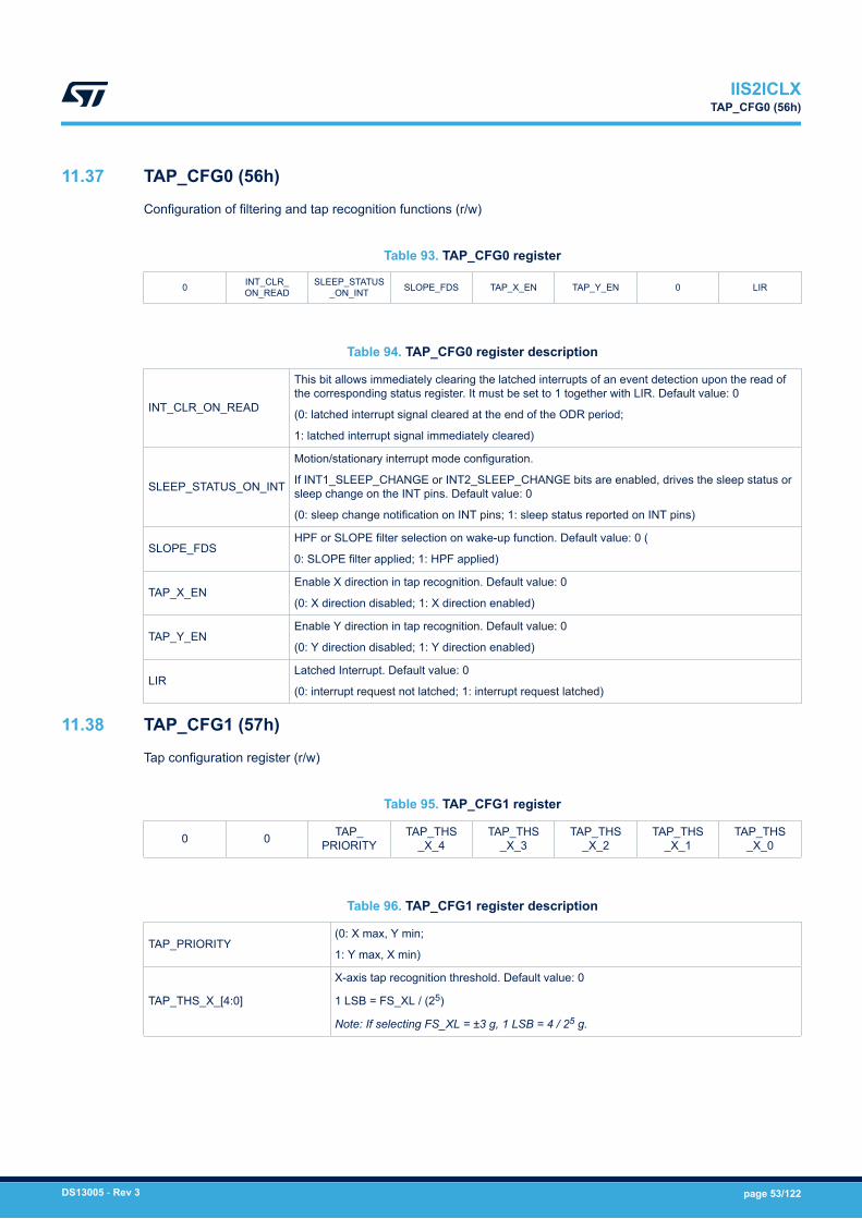
11.37 TAP_CFG0 (56h)
Configuration of filtering and tap recognition functions (r/w)
Table 93. TAP_CFG0 register
0 INT_CLR_ON_READ
SLEEP_STATUS_ON_INT SLOPE_FDS TAP_X_EN TAP_Y_EN 0 LIR
Table 94. TAP_CFG0 register description
INT_CLR_ON_READ
This bit allows immediately clearing the latched interrupts of an event detection upon the read ofthe corresponding status register. It must be set to 1 together with LIR. Default value: 0
(0: latched interrupt signal cleared at the end of the ODR period;
1: latched interrupt signal immediately cleared)
SLEEP_STATUS_ON_INT
Motion/stationary interrupt mode configuration.
If INT1_SLEEP_CHANGE or INT2_SLEEP_CHANGE bits are enabled, drives the sleep status orsleep change on the INT pins. Default value: 0
(0: sleep change notification on INT pins; 1: sleep status reported on INT pins)
SLOPE_FDSHPF or SLOPE filter selection on wake-up function. Default value: 0 (
0: SLOPE filter applied; 1: HPF applied)
TAP_X_ENEnable X direction in tap recognition. Default value: 0
(0: X direction disabled; 1: X direction enabled)
TAP_Y_ENEnable Y direction in tap recognition. Default value: 0
(0: Y direction disabled; 1: Y direction enabled)
LIRLatched Interrupt. Default value: 0
(0: interrupt request not latched; 1: interrupt request latched)
11.38 TAP_CFG1 (57h)
Tap configuration register (r/w)
Table 95. TAP_CFG1 register
0 0 TAP_PRIORITY
TAP_THS_X_4
TAP_THS_X_3
TAP_THS_X_2
TAP_THS_X_1
TAP_THS_X_0
Table 96. TAP_CFG1 register description
TAP_PRIORITY(0: X max, Y min;
1: Y max, X min)
TAP_THS_X_[4:0]
X-axis tap recognition threshold. Default value: 0
1 LSB = FS_XL / (25)
Note: If selecting FS_XL = ±3 g, 1 LSB = 4 / 25 g.
IIS2ICLXTAP_CFG0 (56h)
DS13005 - Rev 3 page 53/122
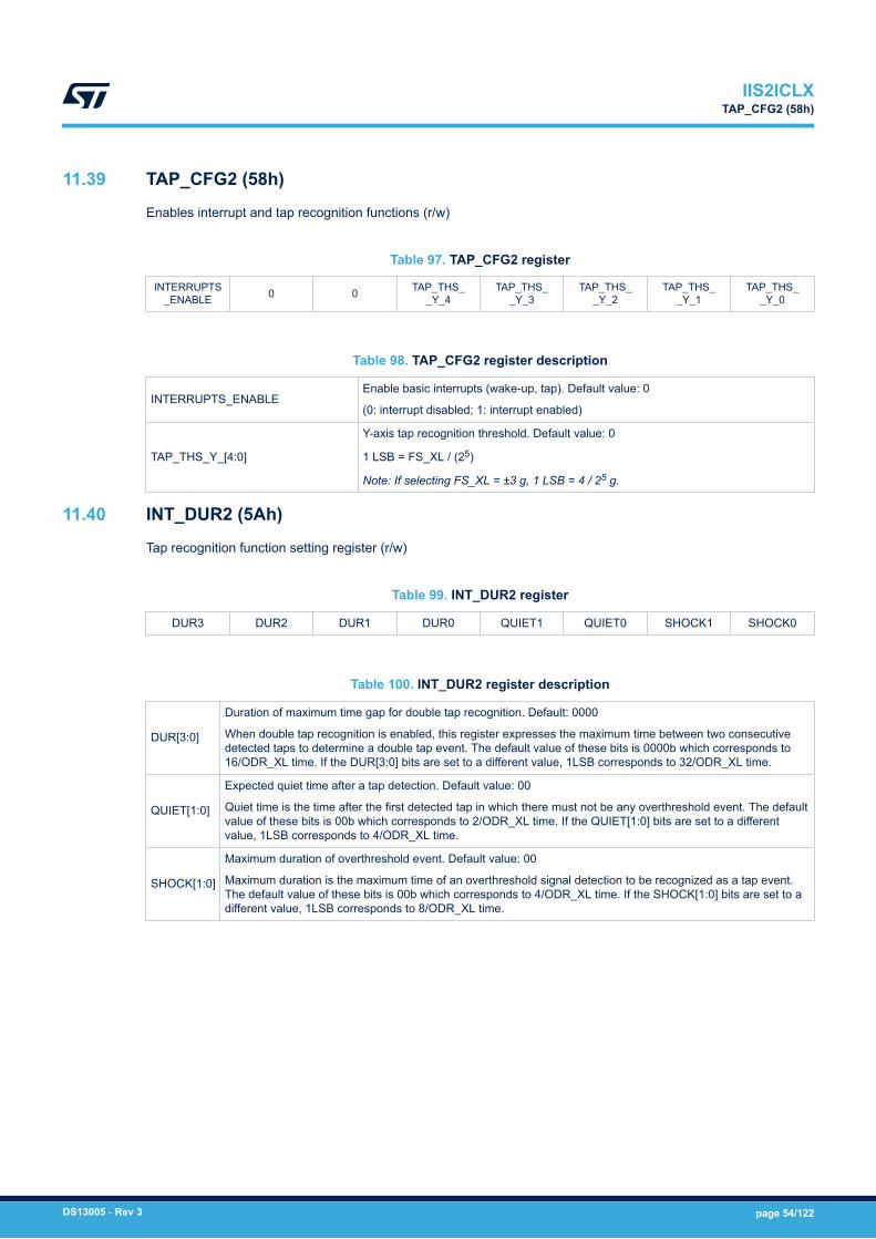
11.39 TAP_CFG2 (58h)
Enables interrupt and tap recognition functions (r/w)
Table 97. TAP_CFG2 register
INTERRUPTS_ENABLE 0 0 TAP_THS_
_Y_4TAP_THS_
_Y_3TAP_THS_
_Y_2TAP_THS_
_Y_1TAP_THS_
_Y_0
Table 98. TAP_CFG2 register description
INTERRUPTS_ENABLEEnable basic interrupts (wake-up, tap). Default value: 0
(0: interrupt disabled; 1: interrupt enabled)
TAP_THS_Y_[4:0]
Y-axis tap recognition threshold. Default value: 0
1 LSB = FS_XL / (25)
Note: If selecting FS_XL = ±3 g, 1 LSB = 4 / 25 g.
11.40 INT_DUR2 (5Ah)
Tap recognition function setting register (r/w)
Table 99. INT_DUR2 register
DUR3 DUR2 DUR1 DUR0 QUIET1 QUIET0 SHOCK1 SHOCK0
Table 100. INT_DUR2 register description
DUR[3:0]
Duration of maximum time gap for double tap recognition. Default: 0000
When double tap recognition is enabled, this register expresses the maximum time between two consecutivedetected taps to determine a double tap event. The default value of these bits is 0000b which corresponds to16/ODR_XL time. If the DUR[3:0] bits are set to a different value, 1LSB corresponds to 32/ODR_XL time.
QUIET[1:0]
Expected quiet time after a tap detection. Default value: 00
Quiet time is the time after the first detected tap in which there must not be any overthreshold event. The defaultvalue of these bits is 00b which corresponds to 2/ODR_XL time. If the QUIET[1:0] bits are set to a differentvalue, 1LSB corresponds to 4/ODR_XL time.
SHOCK[1:0]
Maximum duration of overthreshold event. Default value: 00
Maximum duration is the maximum time of an overthreshold signal detection to be recognized as a tap event.The default value of these bits is 00b which corresponds to 4/ODR_XL time. If the SHOCK[1:0] bits are set to adifferent value, 1LSB corresponds to 8/ODR_XL time.
IIS2ICLXTAP_CFG2 (58h)
DS13005 - Rev 3 page 54/122

11.41 WAKE_UP_THS (5Bh)
Single/double-tap selection and wake-up configuration (r/w)
Table 101. WAKE_UP_THS register
SINGLE_DOUBLE_TAP
USR_OFF_ON_WU WK_THS5 WK_THS4 WK_THS3 WK_THS2 WK_THS1 WK_THS0
Table 102. WAKE_UP_THS register description
SINGLE_DOUBLE_TAP
Single/double-tap event enable. Default: 0
(0: only single-tap event enabled;
1: both single and double-tap events enabled)
USR_OFF_ON_WU Drives the low-pass filtered data with user offset correction (instead of high-pass filtered data) to thewakeup function.
WK_THS[5:0] Threshold for wakeup: 1 LSB weight depends on WAKE_THS_W in WAKE_UP_DUR (5Ch).Default value: 000000
11.42 WAKE_UP_DUR (5Ch)
Wakeup and sleep mode functions duration setting register (r/w)
Table 103. WAKE_UP_DUR register
0 WAKE_DUR1
WAKE_DUR0
WAKE_THS_W
SLEEP_DUR3
SLEEP_DUR2
SLEEP_DUR1
SLEEP_DUR0
Table 104. WAKE_UP_DUR register description
WAKE_DUR[1:0]Wake up duration event. Default: 00
1LSB = 1 ODR_time
WAKE_THS_W
Weight of 1 LSB of wakeup threshold. Default: 0
(0: 1 LSB = FS_XL / (26);
1: 1 LSB = FS_XL / (28))
Note: If selecting FS_XL = ±3 g then:if WAKE_THS_W = 0, 1 LSB = 4 / 26 g; if WAKE_THS_W = 1, 1 LSB = 4 / 28 g.
SLEEP_DUR[3:0]Duration to go in sleep mode. Default value: 0000 (this corresponds to 16 ODR)
1 LSB = 512 ODR
IIS2ICLXWAKE_UP_THS (5Bh)
DS13005 - Rev 3 page 55/122

11.43 MD1_CFG (5Eh)
Functions routing on INT1 register (r/w)
Table 105. MD1_CFG register
INT1_SLEEP_CHANGE
INT1_SINGLE_TAP INT1_WU 0(1) INT1_
DOUBLE_TAP 0(1) INT1_EMB_FUNC INT1_SHUB
1. This bit must be set to '0' for the correct operation of the device.
Table 106. MD1_CFG register description
INT1_SLEEP_CHANGE(1)
Routing of stationary/motion recognition event on INT1. Default: 0
(0: routing of stationary/motion event on INT1 disabled;
1: routing of stationary/motion event on INT1 enabled)
INT1_SINGLE_TAP
Routing of single-tap recognition event on INT1. Default: 0
(0: routing of single-tap event on INT1 disabled;
1: routing of single-tap event on INT1 enabled)
INT1_WU
Routing of wakeup event on INT1. Default value: 0
(0: routing of wakeup event on INT1 disabled;
1: routing of wakeup event on INT1 enabled)
INT1_DOUBLE_TAP
Routing of double-tap event on INT1. Default value: 0
(0: routing of double-tap event on INT1 disabled;
1: routing of double-tap event on INT1 enabled)
INT1_EMB_FUNC
Routing of embedded functions event on INT1. Default value: 0
(0: routing of embedded functions event on INT1 disabled;
1: routing embedded functions event on INT1 enabled)
INT1_SHUB
Routing of sensor hub communication concluded event on INT1.
Default value: 0
(0: routing of sensor hub communication concluded event on INT1 disabled; 1: routing of sensorhub communication concluded event on INT1 enabled)
1. Stationary/motion interrupt mode (sleep change or sleep status) depends on the SLEEP_STATUS_ON_INT bit in theTAP_CFG0 (56h) register.
IIS2ICLXMD1_CFG (5Eh)
DS13005 - Rev 3 page 56/122
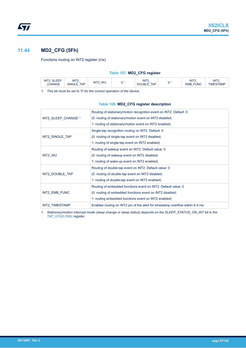
11.44 MD2_CFG (5Fh)
Functions routing on INT2 register (r/w)
Table 107. MD2_CFG register
INT2_SLEEP_CHANGE
INT2_SINGLE_TAP INT2_WU 0(1) INT2_
DOUBLE_TAP 0(1) INT2_EMB_FUNC
INT2_TIMESTAMP
1. This bit must be set to '0' for the correct operation of the device.
Table 108. MD2_CFG register description
INT2_SLEEP_CHANGE(1)
Routing of stationary/motion recognition event on INT2. Default: 0
(0: routing of stationary/motion event on INT2 disabled;
1: routing of stationary/motion event on INT2 enabled)
INT2_SINGLE_TAP
Single-tap recognition routing on INT2. Default: 0
(0: routing of single-tap event on INT2 disabled;
1: routing of single-tap event on INT2 enabled)
INT2_WU
Routing of wakeup event on INT2. Default value: 0
(0: routing of wakeup event on INT2 disabled;
1: routing of wake-up event on INT2 enabled)
INT2_DOUBLE_TAP
Routing of double-tap event on INT2. Default value: 0
(0: routing of double-tap event on INT2 disabled;
1: routing of double-tap event on INT2 enabled)
INT2_EMB_FUNC
Routing of embedded functions event on INT2. Default value: 0
(0: routing of embedded functions event on INT2 disabled;
1: routing embedded functions event on INT2 enabled)
INT2_TIMESTAMP Enables routing on INT2 pin of the alert for timestamp overflow within 6.4 ms.
1. Stationary/motion interrupt mode (sleep change or sleep status) depends on the SLEEP_STATUS_ON_INT bit in theTAP_CFG0 (56h) register.
IIS2ICLXMD2_CFG (5Fh)
DS13005 - Rev 3 page 57/122
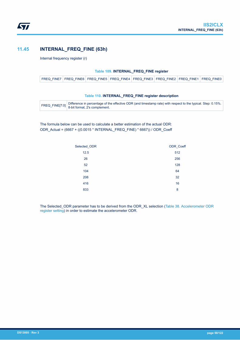
11.45 INTERNAL_FREQ_FINE (63h)
Internal frequency register (r)
Table 109. INTERNAL_FREQ_FINE register
FREQ_FINE7 FREQ_FINE6 FREQ_FINE5 FREQ_FINE4 FREQ_FINE3 FREQ_FINE2 FREQ_FINE1 FREQ_FINE0
Table 110. INTERNAL_FREQ_FINE register description
FREQ_FINE[7:0] Difference in percentage of the effective ODR (and timestamp rate) with respect to the typical. Step: 0.15%.8-bit format, 2's complement.
The formula below can be used to calculate a better estimation of the actual ODR:ODR_Actual = (6667 + ((0.0015 * INTERNAL_FREQ_FINE) * 6667)) / ODR_Coeff
Selected_ODR ODR_Coeff
12.5 512
26 256
52 128
104 64
208 32
416 16
833 8
The Selected_ODR parameter has to be derived from the ODR_XL selection (Table 38. Accelerometer ODRregister setting) in order to estimate the accelerometer ODR.
IIS2ICLXINTERNAL_FREQ_FINE (63h)
DS13005 - Rev 3 page 58/122
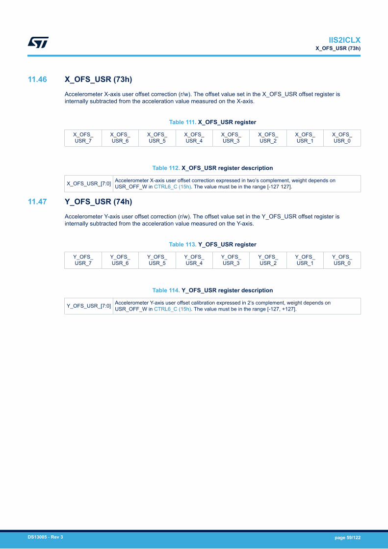
11.46 X_OFS_USR (73h)
Accelerometer X-axis user offset correction (r/w). The offset value set in the X_OFS_USR offset register isinternally subtracted from the acceleration value measured on the X-axis.
Table 111. X_OFS_USR register
X_OFS_USR_7
X_OFS_USR_6
X_OFS_USR_5
X_OFS_USR_4
X_OFS_USR_3
X_OFS_USR_2
X_OFS_USR_1
X_OFS_USR_0
Table 112. X_OFS_USR register description
X_OFS_USR_[7:0] Accelerometer X-axis user offset correction expressed in two’s complement, weight depends onUSR_OFF_W in CTRL6_C (15h). The value must be in the range [-127 127].
11.47 Y_OFS_USR (74h)
Accelerometer Y-axis user offset correction (r/w). The offset value set in the Y_OFS_USR offset register isinternally subtracted from the acceleration value measured on the Y-axis.
Table 113. Y_OFS_USR register
Y_OFS_USR_7
Y_OFS_USR_6
Y_OFS_USR_5
Y_OFS_USR_4
Y_OFS_USR_3
Y_OFS_USR_2
Y_OFS_USR_1
Y_OFS_USR_0
Table 114. Y_OFS_USR register description
Y_OFS_USR_[7:0] Accelerometer Y-axis user offset calibration expressed in 2’s complement, weight depends onUSR_OFF_W in CTRL6_C (15h). The value must be in the range [-127, +127].
IIS2ICLXX_OFS_USR (73h)
DS13005 - Rev 3 page 59/122
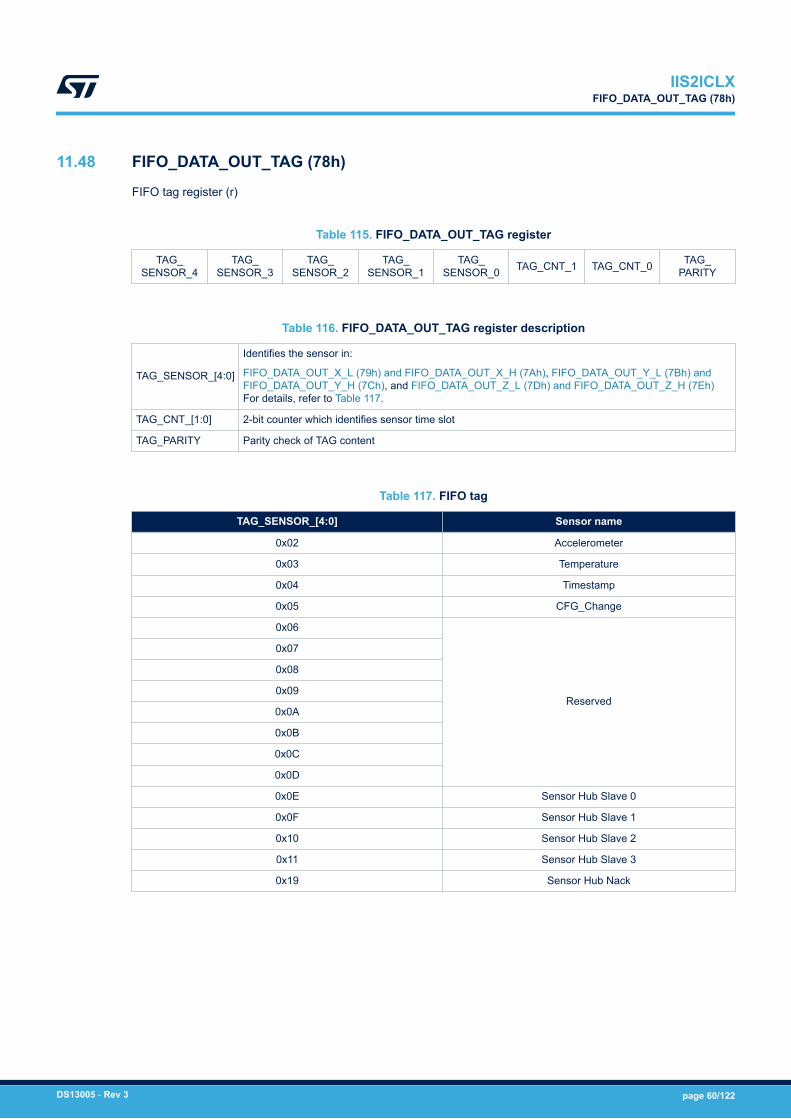
11.48 FIFO_DATA_OUT_TAG (78h)
FIFO tag register (r)
Table 115. FIFO_DATA_OUT_TAG register
TAG_SENSOR_4
TAG_SENSOR_3
TAG_SENSOR_2
TAG_SENSOR_1
TAG_SENSOR_0 TAG_CNT_1 TAG_CNT_0 TAG_
PARITY
Table 116. FIFO_DATA_OUT_TAG register description
TAG_SENSOR_[4:0]
Identifies the sensor in:
FIFO_DATA_OUT_X_L (79h) and FIFO_DATA_OUT_X_H (7Ah), FIFO_DATA_OUT_Y_L (7Bh) andFIFO_DATA_OUT_Y_H (7Ch), and FIFO_DATA_OUT_Z_L (7Dh) and FIFO_DATA_OUT_Z_H (7Eh)For details, refer to Table 117.
TAG_CNT_[1:0] 2-bit counter which identifies sensor time slot
TAG_PARITY Parity check of TAG content
Table 117. FIFO tag
TAG_SENSOR_[4:0] Sensor name
0x02 Accelerometer
0x03 Temperature
0x04 Timestamp
0x05 CFG_Change
0x06
Reserved
0x07
0x08
0x09
0x0A
0x0B
0x0C
0x0D
0x0E Sensor Hub Slave 0
0x0F Sensor Hub Slave 1
0x10 Sensor Hub Slave 2
0x11 Sensor Hub Slave 3
0x19 Sensor Hub Nack
IIS2ICLXFIFO_DATA_OUT_TAG (78h)
DS13005 - Rev 3 page 60/122

11.49 FIFO_DATA_OUT_X_L (79h) and FIFO_DATA_OUT_X_H (7Ah)
FIFO data output X (r)
Table 118. FIFO_DATA_OUT_X_H and FIFO_DATA_OUT_X_L registers
D15 D14 D13 D12 D11 D10 D9 D8
D7 D6 D5 D4 D3 D2 D1 D0
Table 119. FIFO_DATA_OUT_X_H and FIFO_DATA_OUT_X_L register description
D[15:0] FIFO X-axis output
11.50 FIFO_DATA_OUT_Y_L (7Bh) and FIFO_DATA_OUT_Y_H (7Ch)
FIFO data output Y (r)
Table 120. FIFO_DATA_OUT_Y_H and FIFO_DATA_OUT_Y_L registers
D15 D14 D13 D12 D11 D10 D9 D8
D7 D6 D5 D4 D3 D2 D1 D0
Table 121. FIFO_DATA_OUT_Y_H and FIFO_DATA_OUT_Y_L register description
D[15:0] FIFO Y-axis output
11.51 FIFO_DATA_OUT_Z_L (7Dh) and FIFO_DATA_OUT_Z_H (7Eh)
FIFO data output Z (r)
Table 122. FIFO_DATA_OUT_Z_H and FIFO_DATA_OUT_Z_L registers
D15 D14 D13 D12 D11 D10 D9 D8
D7 D6 D5 D4 D3 D2 D1 D0
Table 123. FIFO_DATA_OUT_Z_H and FIFO_DATA_OUT_Z_L register description
D[15:0] FIFO Z-axis output
Note: Fields related to the Z-axis are intended for usage in conjunction with an external sensor.
IIS2ICLXFIFO_DATA_OUT_X_L (79h) and FIFO_DATA_OUT_X_H (7Ah)
DS13005 - Rev 3 page 61/122
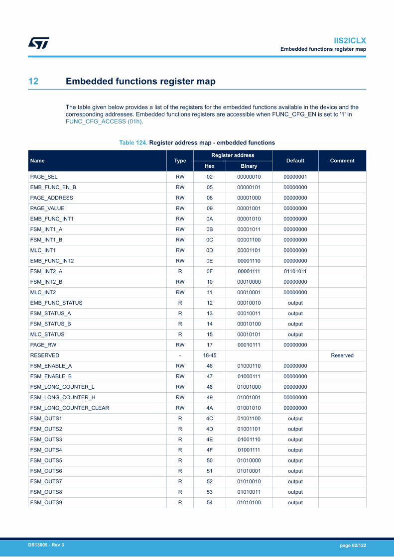
12 Embedded functions register map
The table given below provides a list of the registers for the embedded functions available in the device and thecorresponding addresses. Embedded functions registers are accessible when FUNC_CFG_EN is set to '1' inFUNC_CFG_ACCESS (01h).
Table 124. Register address map - embedded functions
Name TypeRegister address
Default CommentHex Binary
PAGE_SEL RW 02 00000010 00000001
EMB_FUNC_EN_B RW 05 00000101 00000000
PAGE_ADDRESS RW 08 00001000 00000000
PAGE_VALUE RW 09 00001001 00000000
EMB_FUNC_INT1 RW 0A 00001010 00000000
FSM_INT1_A RW 0B 00001011 00000000
FSM_INT1_B RW 0C 00001100 00000000
MLC_INT1 RW 0D 00001101 00000000
EMB_FUNC_INT2 RW 0E 00001110 00000000
FSM_INT2_A R 0F 00001111 01101011
FSM_INT2_B RW 10 00010000 00000000
MLC_INT2 RW 11 00010001 00000000
EMB_FUNC_STATUS R 12 00010010 output
FSM_STATUS_A R 13 00010011 output
FSM_STATUS_B R 14 00010100 output
MLC_STATUS R 15 00010101 output
PAGE_RW RW 17 00010111 00000000
RESERVED - 18-45 Reserved
FSM_ENABLE_A RW 46 01000110 00000000
FSM_ENABLE_B RW 47 01000111 00000000
FSM_LONG_COUNTER_L RW 48 01001000 00000000
FSM_LONG_COUNTER_H RW 49 01001001 00000000
FSM_LONG_COUNTER_CLEAR RW 4A 01001010 00000000
FSM_OUTS1 R 4C 01001100 output
FSM_OUTS2 R 4D 01001101 output
FSM_OUTS3 R 4E 01001110 output
FSM_OUTS4 R 4F 01001111 output
FSM_OUTS5 R 50 01010000 output
FSM_OUTS6 R 51 01010001 output
FSM_OUTS7 R 52 01010010 output
FSM_OUTS8 R 53 01010011 output
FSM_OUTS9 R 54 01010100 output
IIS2ICLXEmbedded functions register map
DS13005 - Rev 3 page 62/122
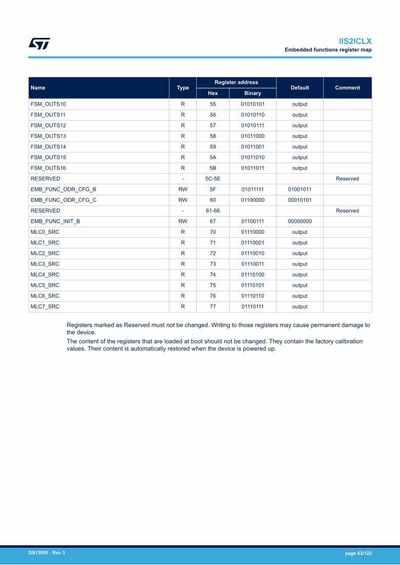
Name TypeRegister address
Default CommentHex Binary
FSM_OUTS10 R 55 01010101 output
FSM_OUTS11 R 56 01010110 output
FSM_OUTS12 R 57 01010111 output
FSM_OUTS13 R 58 01011000 output
FSM_OUTS14 R 59 01011001 output
FSM_OUTS15 R 5A 01011010 output
FSM_OUTS16 R 5B 01011011 output
RESERVED - 5C-5E Reserved
EMB_FUNC_ODR_CFG_B RW 5F 01011111 01001011
EMB_FUNC_ODR_CFG_C RW 60 01100000 00010101
RESERVED - 61-66 Reserved
EMB_FUNC_INIT_B RW 67 01100111 00000000
MLC0_SRC R 70 01110000 output
MLC1_SRC R 71 01110001 output
MLC2_SRC R 72 01110010 output
MLC3_SRC R 73 01110011 output
MLC4_SRC R 74 01110100 output
MLC5_SRC R 75 01110101 output
MLC6_SRC R 76 01110110 output
MLC7_SRC R 77 01110111 output
Registers marked as Reserved must not be changed. Writing to those registers may cause permanent damage tothe device.The content of the registers that are loaded at boot should not be changed. They contain the factory calibrationvalues. Their content is automatically restored when the device is powered up.
IIS2ICLXEmbedded functions register map
DS13005 - Rev 3 page 63/122
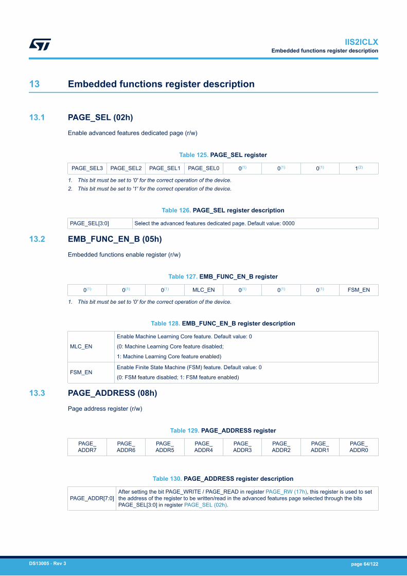
13 Embedded functions register description
13.1 PAGE_SEL (02h)
Enable advanced features dedicated page (r/w)
Table 125. PAGE_SEL register
PAGE_SEL3 PAGE_SEL2 PAGE_SEL1 PAGE_SEL0 0(1) 0(1) 0(1) 1(2)
1. This bit must be set to '0' for the correct operation of the device.2. This bit must be set to '1' for the correct operation of the device.
Table 126. PAGE_SEL register description
PAGE_SEL[3:0] Select the advanced features dedicated page. Default value: 0000
13.2 EMB_FUNC_EN_B (05h)
Embedded functions enable register (r/w)
Table 127. EMB_FUNC_EN_B register
0(1) 0(1) 0(1) MLC_EN 0(1) 0(1) 0(1) FSM_EN
1. This bit must be set to '0' for the correct operation of the device.
Table 128. EMB_FUNC_EN_B register description
MLC_EN
Enable Machine Learning Core feature. Default value: 0
(0: Machine Learning Core feature disabled;
1: Machine Learning Core feature enabled)
FSM_ENEnable Finite State Machine (FSM) feature. Default value: 0
(0: FSM feature disabled; 1: FSM feature enabled)
13.3 PAGE_ADDRESS (08h)
Page address register (r/w)
Table 129. PAGE_ADDRESS register
PAGE_ADDR7
PAGE_ADDR6
PAGE_ADDR5
PAGE_ADDR4
PAGE_ADDR3
PAGE_ADDR2
PAGE_ADDR1
PAGE_ADDR0
Table 130. PAGE_ADDRESS register description
PAGE_ADDR[7:0]After setting the bit PAGE_WRITE / PAGE_READ in register PAGE_RW (17h), this register is used to setthe address of the register to be written/read in the advanced features page selected through the bitsPAGE_SEL[3:0] in register PAGE_SEL (02h).
IIS2ICLXEmbedded functions register description
DS13005 - Rev 3 page 64/122
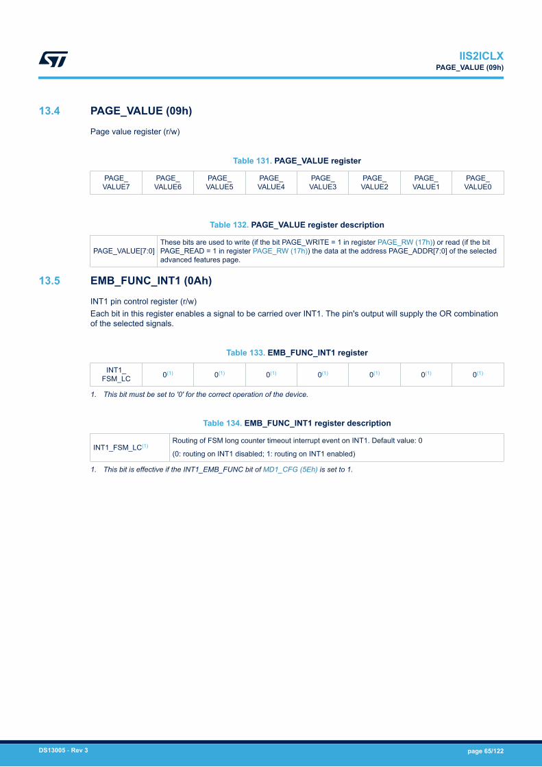
13.4 PAGE_VALUE (09h)
Page value register (r/w)
Table 131. PAGE_VALUE register
PAGE_VALUE7
PAGE_VALUE6
PAGE_VALUE5
PAGE_VALUE4
PAGE_VALUE3
PAGE_VALUE2
PAGE_VALUE1
PAGE_VALUE0
Table 132. PAGE_VALUE register description
PAGE_VALUE[7:0]These bits are used to write (if the bit PAGE_WRITE = 1 in register PAGE_RW (17h)) or read (if the bitPAGE_READ = 1 in register PAGE_RW (17h)) the data at the address PAGE_ADDR[7:0] of the selectedadvanced features page.
13.5 EMB_FUNC_INT1 (0Ah)
INT1 pin control register (r/w)Each bit in this register enables a signal to be carried over INT1. The pin's output will supply the OR combinationof the selected signals.
Table 133. EMB_FUNC_INT1 register
INT1_FSM_LC 0(1) 0(1) 0(1) 0(1) 0(1) 0(1) 0(1)
1. This bit must be set to '0' for the correct operation of the device.
Table 134. EMB_FUNC_INT1 register description
INT1_FSM_LC(1)Routing of FSM long counter timeout interrupt event on INT1. Default value: 0
(0: routing on INT1 disabled; 1: routing on INT1 enabled)
1. This bit is effective if the INT1_EMB_FUNC bit of MD1_CFG (5Eh) is set to 1.
IIS2ICLXPAGE_VALUE (09h)
DS13005 - Rev 3 page 65/122
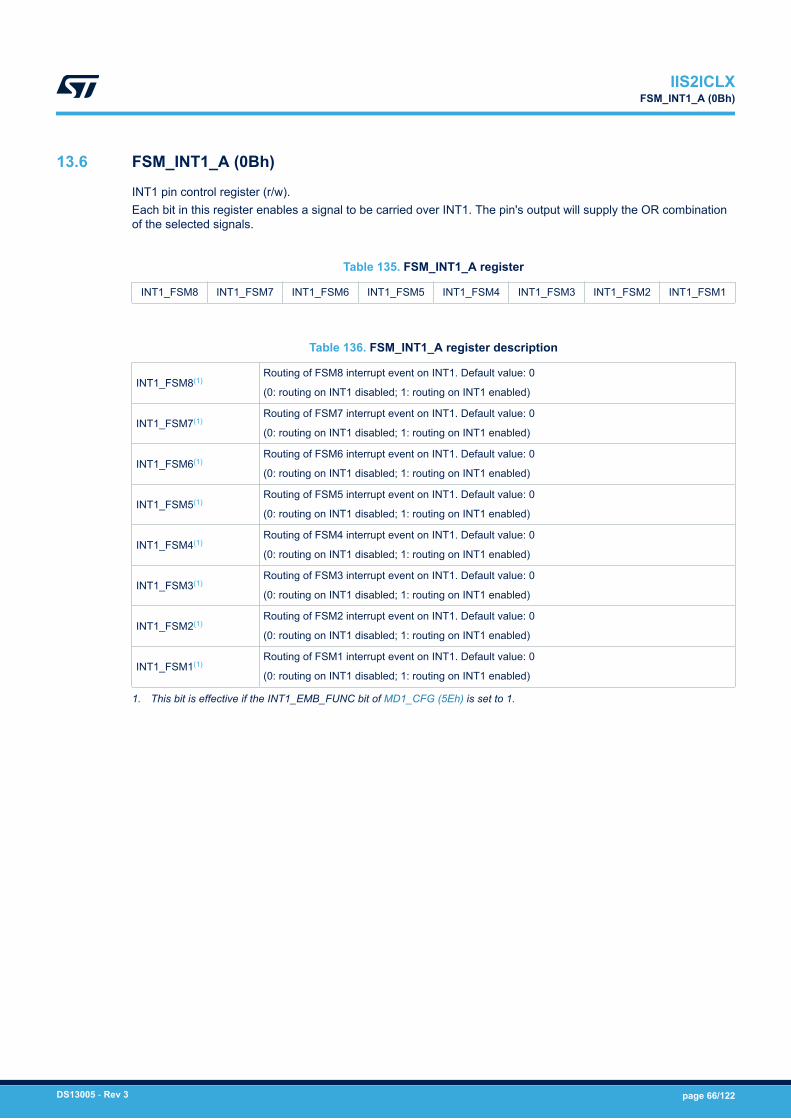
13.6 FSM_INT1_A (0Bh)
INT1 pin control register (r/w).Each bit in this register enables a signal to be carried over INT1. The pin's output will supply the OR combinationof the selected signals.
Table 135. FSM_INT1_A register
INT1_FSM8 INT1_FSM7 INT1_FSM6 INT1_FSM5 INT1_FSM4 INT1_FSM3 INT1_FSM2 INT1_FSM1
Table 136. FSM_INT1_A register description
INT1_FSM8(1)Routing of FSM8 interrupt event on INT1. Default value: 0
(0: routing on INT1 disabled; 1: routing on INT1 enabled)
INT1_FSM7(1)Routing of FSM7 interrupt event on INT1. Default value: 0
(0: routing on INT1 disabled; 1: routing on INT1 enabled)
INT1_FSM6(1)Routing of FSM6 interrupt event on INT1. Default value: 0
(0: routing on INT1 disabled; 1: routing on INT1 enabled)
INT1_FSM5(1)Routing of FSM5 interrupt event on INT1. Default value: 0
(0: routing on INT1 disabled; 1: routing on INT1 enabled)
INT1_FSM4(1)Routing of FSM4 interrupt event on INT1. Default value: 0
(0: routing on INT1 disabled; 1: routing on INT1 enabled)
INT1_FSM3(1)Routing of FSM3 interrupt event on INT1. Default value: 0
(0: routing on INT1 disabled; 1: routing on INT1 enabled)
INT1_FSM2(1)Routing of FSM2 interrupt event on INT1. Default value: 0
(0: routing on INT1 disabled; 1: routing on INT1 enabled)
INT1_FSM1(1)Routing of FSM1 interrupt event on INT1. Default value: 0
(0: routing on INT1 disabled; 1: routing on INT1 enabled)
1. This bit is effective if the INT1_EMB_FUNC bit of MD1_CFG (5Eh) is set to 1.
IIS2ICLXFSM_INT1_A (0Bh)
DS13005 - Rev 3 page 66/122

13.7 FSM_INT1_B (0Ch)
INT1 pin control register (r/w).Each bit in this register enables a signal to be carried over INT1. The pin's output will supply the OR combinationof the selected signals.
Table 137. FSM_INT1_B register
INT1_FSM16 INT1_FSM15 INT1_FSM14 INT1_FSM13 INT1_FSM12 INT1_FSM11 INT1_FSM10 INT1_FSM9
Table 138. FSM_INT1_B register description
INT1_FSM16(1)Routing of FSM16 interrupt event on INT1. Default value: 0
(0: routing on INT1 disabled; 1: routing on INT1 enabled)
INT1_FSM15(1)Routing of FSM15 interrupt event on INT1. Default value: 0
(0: routing on INT1 disabled; 1: routing on INT1 enabled)
INT1_FSM14(1)Routing of FSM14 interrupt event on INT1. Default value: 0
(0: routing on INT1 disabled; 1: routing on INT1 enabled)
INT1_FSM13(1)Routing of FSM13 interrupt event on INT1. Default value: 0
(0: routing on INT1 disabled; 1: routing on INT1 enabled)
INT1_FSM12(1)Routing of FSM12 interrupt event on INT1. Default value: 0
(0: routing on INT1 disabled; 1: routing on INT1 enabled)
INT1_FSM11(1)Routing of FSM11 interrupt event on INT1. Default value: 0
(0: routing on INT1 disabled; 1: routing on INT1 enabled)
INT1_FSM10(1)Routing of FSM10 interrupt event on INT1. Default value: 0
(0: routing on INT1 disabled; 1: routing on INT1 enabled)
INT1_FSM9(1)Routing of FSM9 interrupt event on INT1. Default value: 0
(0: routing on INT1 disabled; 1: routing on INT1 enabled)
1. This bit is effective if the INT1_EMB_FUNC bit of MD1_CFG (5Eh) is set to 1.
IIS2ICLXFSM_INT1_B (0Ch)
DS13005 - Rev 3 page 67/122

13.8 MLC_INT1 (0Dh)
INT1 pin control register (r/w).Each bit in this register enables a signal to be carried over INT1. The pin's output will supply the OR combinationof the selected signals.
Table 139. MLC_INT1 register
INT1_MLC8 INT1_MLC7 INT1_MLC6 INT1_MLC5 INT1_MLC4 INT1_MLC3 INT1_MLC2 INT1_MLC1
Table 140. MLC_INT1 register description
INT1_MLC8Routing of MLC8 interrupt event on INT1. Default value: 0
(0: routing on INT1 disabled; 1: routing on INT1 enabled)
INT1_MLC7Routing of MLC7 interrupt event on INT1. Default value: 0
(0: routing on INT1 disabled; 1: routing on INT1 enabled)
INT1_MLC6Routing of MLC6 interrupt event on INT1. Default value: 0
(0: routing on INT1 disabled; 1: routing on INT1 enabled)
INT1_MLC5Routing of MLC5 interrupt event on INT1. Default value: 0
(0: routing on INT1 disabled; 1: routing on INT1 enabled)
INT1_MLC4Routing of MLC4 interrupt event on INT1. Default value: 0
(0: routing on INT1 disabled; 1: routing on INT1 enabled)
INT1_MLC3Routing of MLC3 interrupt event on INT1. Default value: 0
(0: routing on INT1 disabled; 1: routing on INT1 enabled)
INT1_MLC2Routing of MLC2 interrupt event on INT1. Default value: 0
(0: routing on INT1 disabled; 1: routing on INT1 enabled)
INT1_MLC1Routing of MLC1 interrupt event on INT1. Default value: 0
(0: routing on INT1 disabled; 1: routing on INT1 enabled)
13.9 EMB_FUNC_INT2 (0Eh)
INT2 pin control register (r/w).Each bit in this register enables a signal to be carried over INT2. The pin's output will supply the OR combinationof the selected signals.
Table 141. EMB_FUNC_INT2 register
INT2_FSM_LC 0(1) 0(1) 0(1) 0(1) 0(1) 0(1) 0(1)
1. This bit must be set to '0' for the correct operation of the device.
Table 142. EMB_FUNC_INT2 register description
INT2_FSM_LC(1)Routing of FSM long counter timeout interrupt event on INT2. Default value: 0
(0: routing on INT2 disabled; 1: routing on INT2 enabled)
1. This bit is effective if the INT2_EMB_FUNC bit of MD2_CFG (5Fh) is set to 1.
IIS2ICLXMLC_INT1 (0Dh)
DS13005 - Rev 3 page 68/122
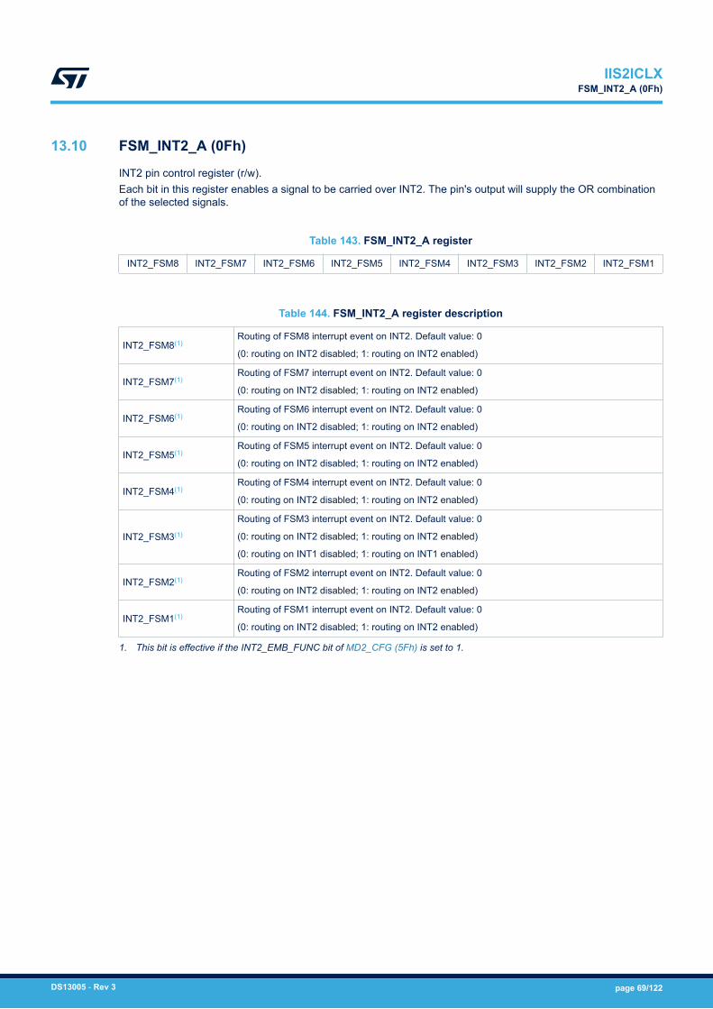
13.10 FSM_INT2_A (0Fh)
INT2 pin control register (r/w).Each bit in this register enables a signal to be carried over INT2. The pin's output will supply the OR combinationof the selected signals.
Table 143. FSM_INT2_A register
INT2_FSM8 INT2_FSM7 INT2_FSM6 INT2_FSM5 INT2_FSM4 INT2_FSM3 INT2_FSM2 INT2_FSM1
Table 144. FSM_INT2_A register description
INT2_FSM8(1)Routing of FSM8 interrupt event on INT2. Default value: 0
(0: routing on INT2 disabled; 1: routing on INT2 enabled)
INT2_FSM7(1)Routing of FSM7 interrupt event on INT2. Default value: 0
(0: routing on INT2 disabled; 1: routing on INT2 enabled)
INT2_FSM6(1)Routing of FSM6 interrupt event on INT2. Default value: 0
(0: routing on INT2 disabled; 1: routing on INT2 enabled)
INT2_FSM5(1)Routing of FSM5 interrupt event on INT2. Default value: 0
(0: routing on INT2 disabled; 1: routing on INT2 enabled)
INT2_FSM4(1)Routing of FSM4 interrupt event on INT2. Default value: 0
(0: routing on INT2 disabled; 1: routing on INT2 enabled)
INT2_FSM3(1)
Routing of FSM3 interrupt event on INT2. Default value: 0
(0: routing on INT2 disabled; 1: routing on INT2 enabled)
(0: routing on INT1 disabled; 1: routing on INT1 enabled)
INT2_FSM2(1)Routing of FSM2 interrupt event on INT2. Default value: 0
(0: routing on INT2 disabled; 1: routing on INT2 enabled)
INT2_FSM1(1)Routing of FSM1 interrupt event on INT2. Default value: 0
(0: routing on INT2 disabled; 1: routing on INT2 enabled)
1. This bit is effective if the INT2_EMB_FUNC bit of MD2_CFG (5Fh) is set to 1.
IIS2ICLXFSM_INT2_A (0Fh)
DS13005 - Rev 3 page 69/122
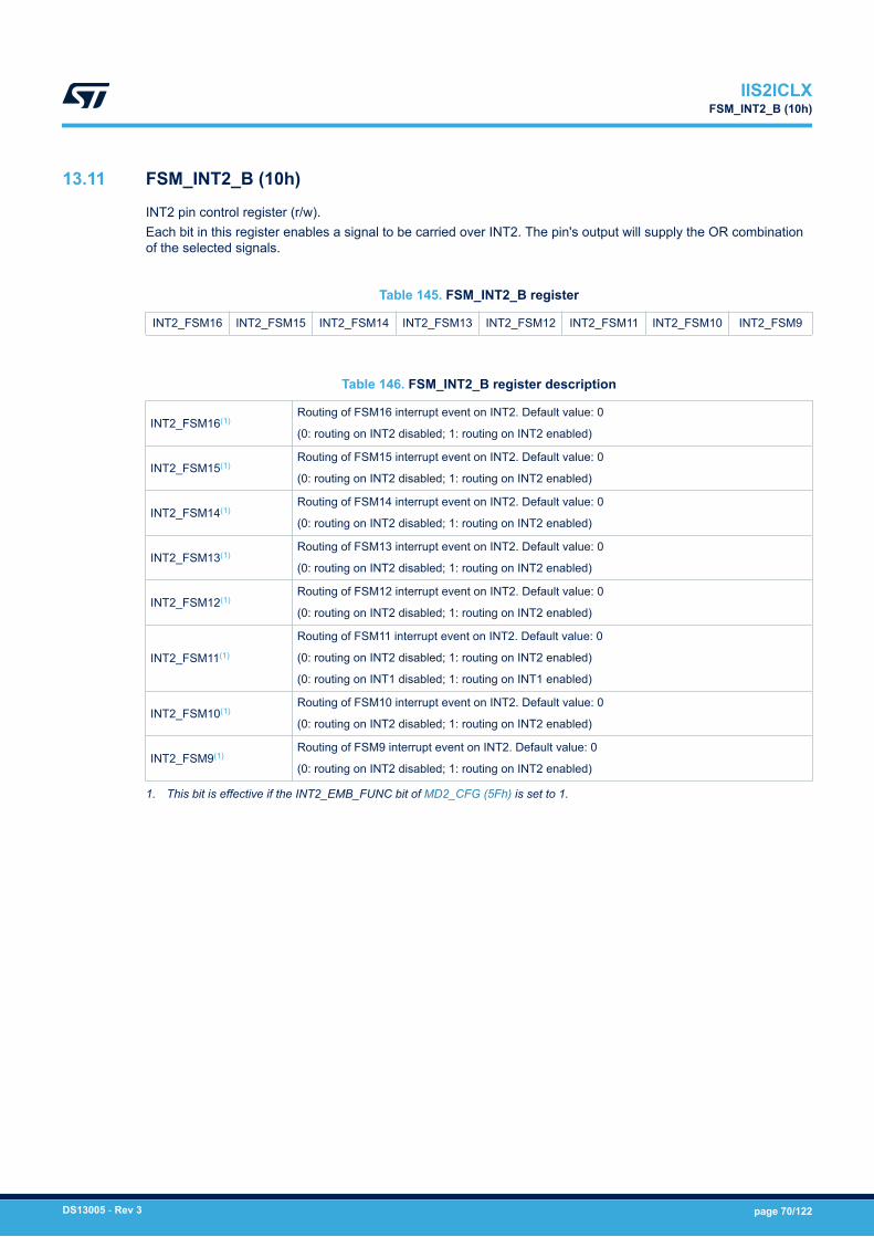
13.11 FSM_INT2_B (10h)
INT2 pin control register (r/w).Each bit in this register enables a signal to be carried over INT2. The pin's output will supply the OR combinationof the selected signals.
Table 145. FSM_INT2_B register
INT2_FSM16 INT2_FSM15 INT2_FSM14 INT2_FSM13 INT2_FSM12 INT2_FSM11 INT2_FSM10 INT2_FSM9
Table 146. FSM_INT2_B register description
INT2_FSM16(1)Routing of FSM16 interrupt event on INT2. Default value: 0
(0: routing on INT2 disabled; 1: routing on INT2 enabled)
INT2_FSM15(1)Routing of FSM15 interrupt event on INT2. Default value: 0
(0: routing on INT2 disabled; 1: routing on INT2 enabled)
INT2_FSM14(1)Routing of FSM14 interrupt event on INT2. Default value: 0
(0: routing on INT2 disabled; 1: routing on INT2 enabled)
INT2_FSM13(1)Routing of FSM13 interrupt event on INT2. Default value: 0
(0: routing on INT2 disabled; 1: routing on INT2 enabled)
INT2_FSM12(1)Routing of FSM12 interrupt event on INT2. Default value: 0
(0: routing on INT2 disabled; 1: routing on INT2 enabled)
INT2_FSM11(1)
Routing of FSM11 interrupt event on INT2. Default value: 0
(0: routing on INT2 disabled; 1: routing on INT2 enabled)
(0: routing on INT1 disabled; 1: routing on INT1 enabled)
INT2_FSM10(1)Routing of FSM10 interrupt event on INT2. Default value: 0
(0: routing on INT2 disabled; 1: routing on INT2 enabled)
INT2_FSM9(1)Routing of FSM9 interrupt event on INT2. Default value: 0
(0: routing on INT2 disabled; 1: routing on INT2 enabled)
1. This bit is effective if the INT2_EMB_FUNC bit of MD2_CFG (5Fh) is set to 1.
IIS2ICLXFSM_INT2_B (10h)
DS13005 - Rev 3 page 70/122
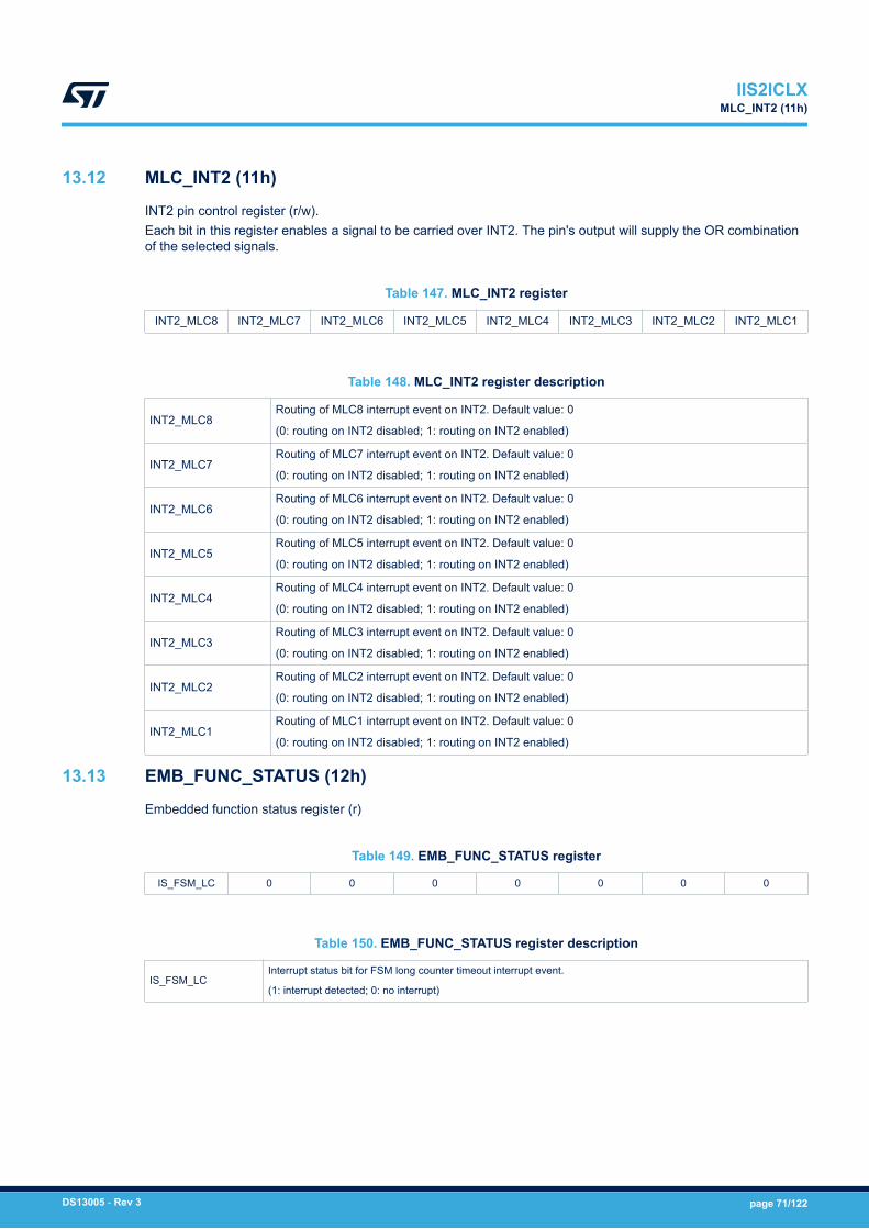
13.12 MLC_INT2 (11h)
INT2 pin control register (r/w).Each bit in this register enables a signal to be carried over INT2. The pin's output will supply the OR combinationof the selected signals.
Table 147. MLC_INT2 register
INT2_MLC8 INT2_MLC7 INT2_MLC6 INT2_MLC5 INT2_MLC4 INT2_MLC3 INT2_MLC2 INT2_MLC1
Table 148. MLC_INT2 register description
INT2_MLC8Routing of MLC8 interrupt event on INT2. Default value: 0
(0: routing on INT2 disabled; 1: routing on INT2 enabled)
INT2_MLC7Routing of MLC7 interrupt event on INT2. Default value: 0
(0: routing on INT2 disabled; 1: routing on INT2 enabled)
INT2_MLC6Routing of MLC6 interrupt event on INT2. Default value: 0
(0: routing on INT2 disabled; 1: routing on INT2 enabled)
INT2_MLC5Routing of MLC5 interrupt event on INT2. Default value: 0
(0: routing on INT2 disabled; 1: routing on INT2 enabled)
INT2_MLC4Routing of MLC4 interrupt event on INT2. Default value: 0
(0: routing on INT2 disabled; 1: routing on INT2 enabled)
INT2_MLC3Routing of MLC3 interrupt event on INT2. Default value: 0
(0: routing on INT2 disabled; 1: routing on INT2 enabled)
INT2_MLC2Routing of MLC2 interrupt event on INT2. Default value: 0
(0: routing on INT2 disabled; 1: routing on INT2 enabled)
INT2_MLC1Routing of MLC1 interrupt event on INT2. Default value: 0
(0: routing on INT2 disabled; 1: routing on INT2 enabled)
13.13 EMB_FUNC_STATUS (12h)
Embedded function status register (r)
Table 149. EMB_FUNC_STATUS register
IS_FSM_LC 0 0 0 0 0 0 0
Table 150. EMB_FUNC_STATUS register description
IS_FSM_LCInterrupt status bit for FSM long counter timeout interrupt event.
(1: interrupt detected; 0: no interrupt)
IIS2ICLXMLC_INT2 (11h)
DS13005 - Rev 3 page 71/122
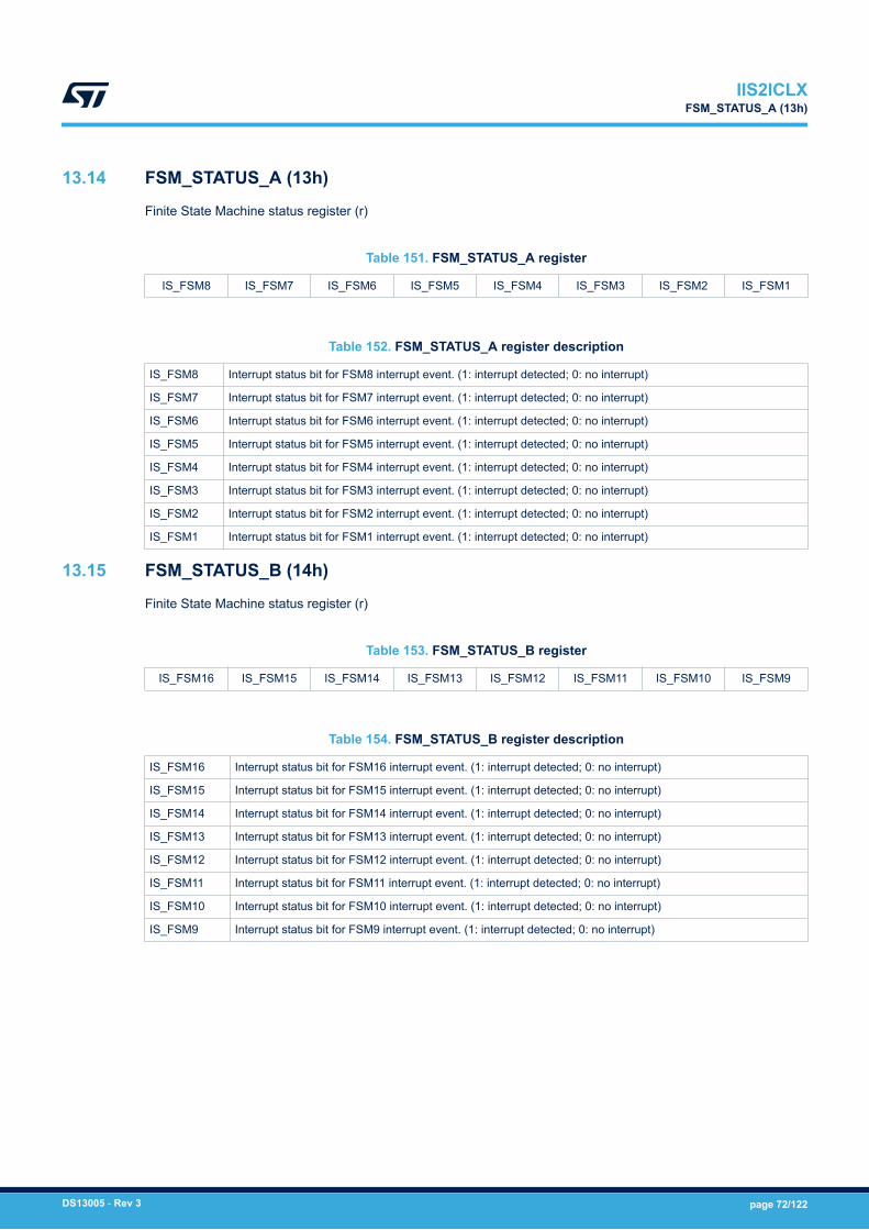
13.14 FSM_STATUS_A (13h)
Finite State Machine status register (r)
Table 151. FSM_STATUS_A register
IS_FSM8 IS_FSM7 IS_FSM6 IS_FSM5 IS_FSM4 IS_FSM3 IS_FSM2 IS_FSM1
Table 152. FSM_STATUS_A register description
IS_FSM8 Interrupt status bit for FSM8 interrupt event. (1: interrupt detected; 0: no interrupt)
IS_FSM7 Interrupt status bit for FSM7 interrupt event. (1: interrupt detected; 0: no interrupt)
IS_FSM6 Interrupt status bit for FSM6 interrupt event. (1: interrupt detected; 0: no interrupt)
IS_FSM5 Interrupt status bit for FSM5 interrupt event. (1: interrupt detected; 0: no interrupt)
IS_FSM4 Interrupt status bit for FSM4 interrupt event. (1: interrupt detected; 0: no interrupt)
IS_FSM3 Interrupt status bit for FSM3 interrupt event. (1: interrupt detected; 0: no interrupt)
IS_FSM2 Interrupt status bit for FSM2 interrupt event. (1: interrupt detected; 0: no interrupt)
IS_FSM1 Interrupt status bit for FSM1 interrupt event. (1: interrupt detected; 0: no interrupt)
13.15 FSM_STATUS_B (14h)
Finite State Machine status register (r)
Table 153. FSM_STATUS_B register
IS_FSM16 IS_FSM15 IS_FSM14 IS_FSM13 IS_FSM12 IS_FSM11 IS_FSM10 IS_FSM9
Table 154. FSM_STATUS_B register description
IS_FSM16 Interrupt status bit for FSM16 interrupt event. (1: interrupt detected; 0: no interrupt)
IS_FSM15 Interrupt status bit for FSM15 interrupt event. (1: interrupt detected; 0: no interrupt)
IS_FSM14 Interrupt status bit for FSM14 interrupt event. (1: interrupt detected; 0: no interrupt)
IS_FSM13 Interrupt status bit for FSM13 interrupt event. (1: interrupt detected; 0: no interrupt)
IS_FSM12 Interrupt status bit for FSM12 interrupt event. (1: interrupt detected; 0: no interrupt)
IS_FSM11 Interrupt status bit for FSM11 interrupt event. (1: interrupt detected; 0: no interrupt)
IS_FSM10 Interrupt status bit for FSM10 interrupt event. (1: interrupt detected; 0: no interrupt)
IS_FSM9 Interrupt status bit for FSM9 interrupt event. (1: interrupt detected; 0: no interrupt)
IIS2ICLXFSM_STATUS_A (13h)
DS13005 - Rev 3 page 72/122
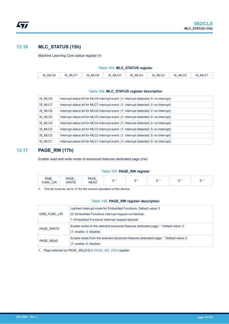
13.16 MLC_STATUS (15h)
Machine Learning Core status register (r)
Table 155. MLC_STATUS register
IS_MLC8 IS_MLC7 IS_MLC6 IS_MLC5 IS_MLC4 IS_MLC3 IS_MLC2 IS_MLC1
Table 156. MLC_STATUS register description
IS_MLC8 Interrupt status bit for MLC8 interrupt event. (1: interrupt detected; 0: no interrupt)
IS_MLC7 Interrupt status bit for MLC7 interrupt event. (1: interrupt detected; 0: no interrupt)
IS_MLC6 Interrupt status bit for MLC6 interrupt event. (1: interrupt detected; 0: no interrupt)
IS_MLC5 Interrupt status bit for MLC5 interrupt event. (1: interrupt detected; 0: no interrupt)
IS_MLC4 Interrupt status bit for MLC4 interrupt event. (1: interrupt detected; 0: no interrupt)
IS_MLC3 Interrupt status bit for MLC3 interrupt event. (1: interrupt detected; 0: no interrupt)
IS_MLC2 Interrupt status bit for MLC2 interrupt event. (1: interrupt detected; 0: no interrupt)
IS_MLC1 Interrupt status bit for MLC1 interrupt event. (1: interrupt detected; 0: no interrupt)
13.17 PAGE_RW (17h)
Enable read and write mode of advanced features dedicated page (r/w)
Table 157. PAGE_RW register
EMB_FUNC_LIR
PAGE_WRITE
PAGE_READ 0(1) 0(1) 0(1) 0(1) 0(1)
1. This bit must be set to '0' for the correct operation of the device.
Table 158. PAGE_RW register description
EMB_FUNC_LIR
Latched Interrupt mode for Embedded Functions. Default value: 0
(0: Embedded Functions interrupt request not latched;
1: Embedded Functions interrupt request latched)
PAGE_WRITEEnable writes to the selected advanced features dedicated page.(1) Default value: 0
(1: enable; 0: disable)
PAGE_READEnable reads from the selected advanced features dedicated page.(1) Default value: 0
(1: enable; 0: disable)
1. Page selected by PAGE_SEL[3:0] in PAGE_SEL (02h) register.
IIS2ICLXMLC_STATUS (15h)
DS13005 - Rev 3 page 73/122
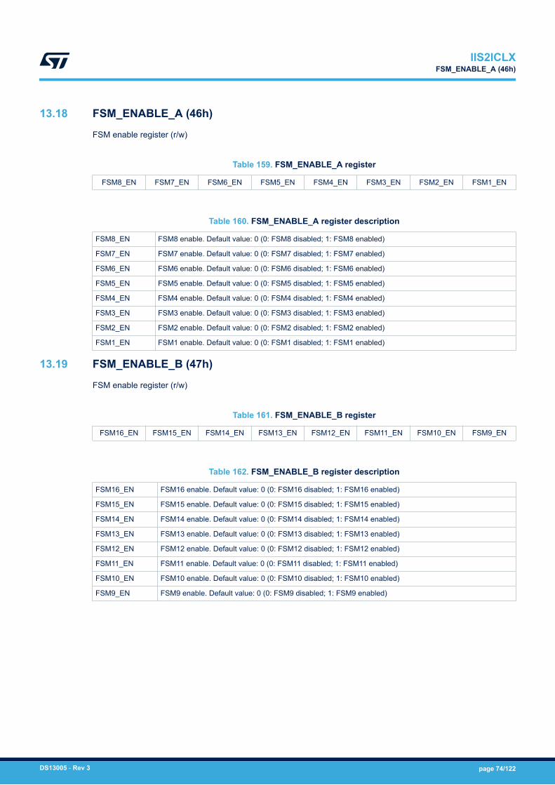
13.18 FSM_ENABLE_A (46h)
FSM enable register (r/w)
Table 159. FSM_ENABLE_A register
FSM8_EN FSM7_EN FSM6_EN FSM5_EN FSM4_EN FSM3_EN FSM2_EN FSM1_EN
Table 160. FSM_ENABLE_A register description
FSM8_EN FSM8 enable. Default value: 0 (0: FSM8 disabled; 1: FSM8 enabled)
FSM7_EN FSM7 enable. Default value: 0 (0: FSM7 disabled; 1: FSM7 enabled)
FSM6_EN FSM6 enable. Default value: 0 (0: FSM6 disabled; 1: FSM6 enabled)
FSM5_EN FSM5 enable. Default value: 0 (0: FSM5 disabled; 1: FSM5 enabled)
FSM4_EN FSM4 enable. Default value: 0 (0: FSM4 disabled; 1: FSM4 enabled)
FSM3_EN FSM3 enable. Default value: 0 (0: FSM3 disabled; 1: FSM3 enabled)
FSM2_EN FSM2 enable. Default value: 0 (0: FSM2 disabled; 1: FSM2 enabled)
FSM1_EN FSM1 enable. Default value: 0 (0: FSM1 disabled; 1: FSM1 enabled)
13.19 FSM_ENABLE_B (47h)
FSM enable register (r/w)
Table 161. FSM_ENABLE_B register
FSM16_EN FSM15_EN FSM14_EN FSM13_EN FSM12_EN FSM11_EN FSM10_EN FSM9_EN
Table 162. FSM_ENABLE_B register description
FSM16_EN FSM16 enable. Default value: 0 (0: FSM16 disabled; 1: FSM16 enabled)
FSM15_EN FSM15 enable. Default value: 0 (0: FSM15 disabled; 1: FSM15 enabled)
FSM14_EN FSM14 enable. Default value: 0 (0: FSM14 disabled; 1: FSM14 enabled)
FSM13_EN FSM13 enable. Default value: 0 (0: FSM13 disabled; 1: FSM13 enabled)
FSM12_EN FSM12 enable. Default value: 0 (0: FSM12 disabled; 1: FSM12 enabled)
FSM11_EN FSM11 enable. Default value: 0 (0: FSM11 disabled; 1: FSM11 enabled)
FSM10_EN FSM10 enable. Default value: 0 (0: FSM10 disabled; 1: FSM10 enabled)
FSM9_EN FSM9 enable. Default value: 0 (0: FSM9 disabled; 1: FSM9 enabled)
IIS2ICLXFSM_ENABLE_A (46h)
DS13005 - Rev 3 page 74/122
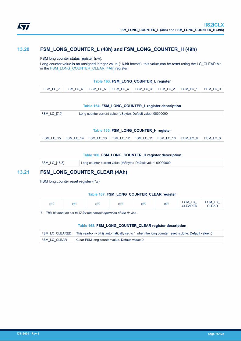
13.20 FSM_LONG_COUNTER_L (48h) and FSM_LONG_COUNTER_H (49h)
FSM long counter status register (r/w).Long counter value is an unsigned integer value (16-bit format); this value can be reset using the LC_CLEAR bitin the FSM_LONG_COUNTER_CLEAR (4Ah) register.
Table 163. FSM_LONG_COUNTER_L register
FSM_LC_7 FSM_LC_6 FSM_LC_5 FSM_LC_4 FSM_LC_3 FSM_LC_2 FSM_LC_1 FSM_LC_0
Table 164. FSM_LONG_COUNTER_L register description
FSM_LC_[7:0] Long counter current value (LSbyte). Default value: 00000000
Table 165. FSM_LONG_COUNTER_H register
FSM_LC_15 FSM_LC_14 FSM_LC_13 FSM_LC_12 FSM_LC_11 FSM_LC_10 FSM_LC_9 FSM_LC_8
Table 166. FSM_LONG_COUNTER_H register description
FSM_LC_[15:8] Long counter current value (MSbyte). Default value: 00000000
13.21 FSM_LONG_COUNTER_CLEAR (4Ah)
FSM long counter reset register (r/w)
Table 167. FSM_LONG_COUNTER_CLEAR register
0(1) 0(1) 0(1) 0(1) 0(1) 0(1) FSM_LC_CLEARED
FSM_LC_CLEAR
1. This bit must be set to '0' for the correct operation of the device.
Table 168. FSM_LONG_COUNTER_CLEAR register description
FSM_LC_CLEARED This read-only bit is automatically set to 1 when the long counter reset is done. Default value: 0
FSM_LC_CLEAR Clear FSM long counter value. Default value: 0
IIS2ICLXFSM_LONG_COUNTER_L (48h) and FSM_LONG_COUNTER_H (49h)
DS13005 - Rev 3 page 75/122
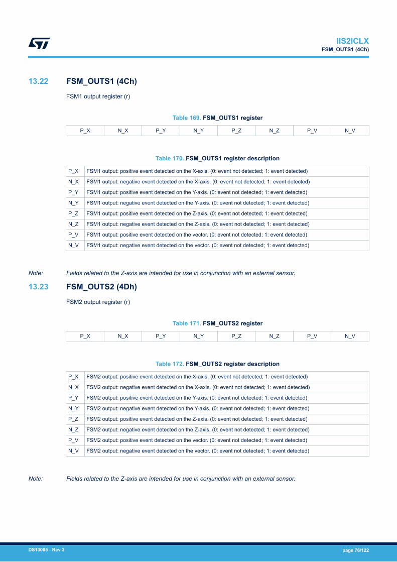
13.22 FSM_OUTS1 (4Ch)
FSM1 output register (r)
Table 169. FSM_OUTS1 register
P_X N_X P_Y N_Y P_Z N_Z P_V N_V
Table 170. FSM_OUTS1 register description
P_X FSM1 output: positive event detected on the X-axis. (0: event not detected; 1: event detected)
N_X FSM1 output: negative event detected on the X-axis. (0: event not detected; 1: event detected)
P_Y FSM1 output: positive event detected on the Y-axis. (0: event not detected; 1: event detected)
N_Y FSM1 output: negative event detected on the Y-axis. (0: event not detected; 1: event detected)
P_Z FSM1 output: positive event detected on the Z-axis. (0: event not detected; 1: event detected)
N_Z FSM1 output: negative event detected on the Z-axis. (0: event not detected; 1: event detected)
P_V FSM1 output: positive event detected on the vector. (0: event not detected; 1: event detected)
N_V FSM1 output: negative event detected on the vector. (0: event not detected; 1: event detected)
Note: Fields related to the Z-axis are intended for use in conjunction with an external sensor.
13.23 FSM_OUTS2 (4Dh)
FSM2 output register (r)
Table 171. FSM_OUTS2 register
P_X N_X P_Y N_Y P_Z N_Z P_V N_V
Table 172. FSM_OUTS2 register description
P_X FSM2 output: positive event detected on the X-axis. (0: event not detected; 1: event detected)
N_X FSM2 output: negative event detected on the X-axis. (0: event not detected; 1: event detected)
P_Y FSM2 output: positive event detected on the Y-axis. (0: event not detected; 1: event detected)
N_Y FSM2 output: negative event detected on the Y-axis. (0: event not detected; 1: event detected)
P_Z FSM2 output: positive event detected on the Z-axis. (0: event not detected; 1: event detected)
N_Z FSM2 output: negative event detected on the Z-axis. (0: event not detected; 1: event detected)
P_V FSM2 output: positive event detected on the vector. (0: event not detected; 1: event detected)
N_V FSM2 output: negative event detected on the vector. (0: event not detected; 1: event detected)
Note: Fields related to the Z-axis are intended for use in conjunction with an external sensor.
IIS2ICLXFSM_OUTS1 (4Ch)
DS13005 - Rev 3 page 76/122
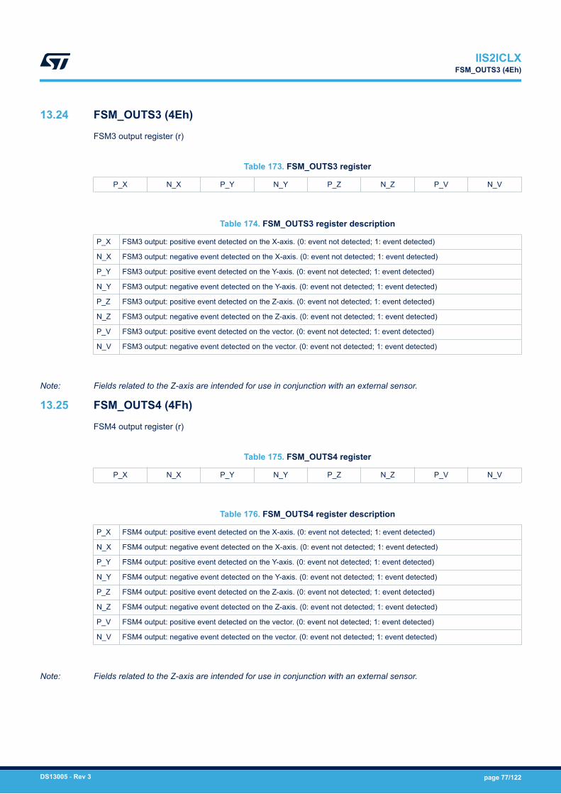
13.24 FSM_OUTS3 (4Eh)
FSM3 output register (r)
Table 173. FSM_OUTS3 register
P_X N_X P_Y N_Y P_Z N_Z P_V N_V
Table 174. FSM_OUTS3 register description
P_X FSM3 output: positive event detected on the X-axis. (0: event not detected; 1: event detected)
N_X FSM3 output: negative event detected on the X-axis. (0: event not detected; 1: event detected)
P_Y FSM3 output: positive event detected on the Y-axis. (0: event not detected; 1: event detected)
N_Y FSM3 output: negative event detected on the Y-axis. (0: event not detected; 1: event detected)
P_Z FSM3 output: positive event detected on the Z-axis. (0: event not detected; 1: event detected)
N_Z FSM3 output: negative event detected on the Z-axis. (0: event not detected; 1: event detected)
P_V FSM3 output: positive event detected on the vector. (0: event not detected; 1: event detected)
N_V FSM3 output: negative event detected on the vector. (0: event not detected; 1: event detected)
Note: Fields related to the Z-axis are intended for use in conjunction with an external sensor.
13.25 FSM_OUTS4 (4Fh)
FSM4 output register (r)
Table 175. FSM_OUTS4 register
P_X N_X P_Y N_Y P_Z N_Z P_V N_V
Table 176. FSM_OUTS4 register description
P_X FSM4 output: positive event detected on the X-axis. (0: event not detected; 1: event detected)
N_X FSM4 output: negative event detected on the X-axis. (0: event not detected; 1: event detected)
P_Y FSM4 output: positive event detected on the Y-axis. (0: event not detected; 1: event detected)
N_Y FSM4 output: negative event detected on the Y-axis. (0: event not detected; 1: event detected)
P_Z FSM4 output: positive event detected on the Z-axis. (0: event not detected; 1: event detected)
N_Z FSM4 output: negative event detected on the Z-axis. (0: event not detected; 1: event detected)
P_V FSM4 output: positive event detected on the vector. (0: event not detected; 1: event detected)
N_V FSM4 output: negative event detected on the vector. (0: event not detected; 1: event detected)
Note: Fields related to the Z-axis are intended for use in conjunction with an external sensor.
IIS2ICLXFSM_OUTS3 (4Eh)
DS13005 - Rev 3 page 77/122

13.26 FSM_OUTS5 (50h)
FSM5 output register (r)
Table 177. FSM_OUTS5 register
P_X N_X P_Y N_Y P_Z N_Z P_V N_V
Table 178. FSM_OUTS5 register description
P_X FSM5 output: positive event detected on the X-axis. (0: event not detected; 1: event detected)
N_X FSM5 output: negative event detected on the X-axis. (0: event not detected; 1: event detected)
P_Y FSM5 output: positive event detected on the Y-axis. (0: event not detected; 1: event detected)
N_Y FSM5 output: negative event detected on the Y-axis. (0: event not detected; 1: event detected)
P_Z FSM5 output: positive event detected on the Z-axis. (0: event not detected; 1: event detected)
N_Z FSM5 output: negative event detected on the Z-axis. (0: event not detected; 1: event detected)
P_V FSM5 output: positive event detected on the vector. (0: event not detected; 1: event detected)
N_V FSM5 output: negative event detected on the vector. (0: event not detected; 1: event detected)
Note: Fields related to the Z-axis are intended for use in conjunction with an external sensor.
13.27 FSM_OUTS6 (51h)
FSM6 output register (r)
Table 179. FSM_OUTS6 register
P_X N_X P_Y N_Y P_Z N_Z P_V N_V
Table 180. FSM_OUTS6 register description
P_X FSM6 output: positive event detected on the X-axis. (0: event not detected; 1: event detected)
N_X FSM6 output: negative event detected on the X-axis. (0: event not detected; 1: event detected)
P_Y FSM6 output: positive event detected on the Y-axis. (0: event not detected; 1: event detected)
N_Y FSM6 output: negative event detected on the Y-axis. (0: event not detected; 1: event detected)
P_Z FSM6 output: positive event detected on the Z-axis. (0: event not detected; 1: event detected)
N_Z FSM6 output: negative event detected on the Z-axis. (0: event not detected; 1: event detected)
P_V FSM6 output: positive event detected on the vector. (0: event not detected; 1: event detected)
N_V FSM6 output: negative event detected on the vector. (0: event not detected; 1: event detected)
Note: Fields related to the Z-axis are intended for use in conjunction with an external sensor.
IIS2ICLXFSM_OUTS5 (50h)
DS13005 - Rev 3 page 78/122

13.28 FSM_OUTS7 (52h)
FSM7 output register (r)
Table 181. FSM_OUTS7 register
P_X N_X P_Y N_Y P_Z N_Z P_V N_V
Table 182. FSM_OUTS7 register description
P_X FSM7 output: positive event detected on the X-axis. (0: event not detected; 1: event detected)
N_X FSM7 output: negative event detected on the X-axis. (0: event not detected; 1: event detected)
P_Y FSM7 output: positive event detected on the Y-axis. (0: event not detected; 1: event detected)
N_Y FSM7 output: negative event detected on the Y-axis. (0: event not detected; 1: event detected)
P_Z FSM7 output: positive event detected on the Z-axis. (0: event not detected; 1: event detected)
N_Z FSM7 output: negative event detected on the Z-axis. (0: event not detected; 1: event detected)
P_V FSM7 output: positive event detected on the vector. (0: event not detected; 1: event detected)
N_V FSM7 output: negative event detected on the vector. (0: event not detected; 1: event detected)
Note: Fields related to the Z-axis are intended for use in conjunction with an external sensor.
13.29 FSM_OUTS8 (53h)
FSM8 output register (r)
Table 183. FSM_OUTS8 register
P_X N_X P_Y N_Y P_Z N_Z P_V N_V
Table 184. FSM_OUTS8 register description
P_X FSM8 output: positive event detected on the X-axis. (0: event not detected; 1: event detected)
N_X FSM8 output: negative event detected on the X-axis. (0: event not detected; 1: event detected)
P_Y FSM8 output: positive event detected on the Y-axis. (0: event not detected; 1: event detected)
N_Y FSM8 output: negative event detected on the Y-axis. (0: event not detected; 1: event detected)
P_Z FSM8 output: positive event detected on the Z-axis. (0: event not detected; 1: event detected)
N_Z FSM8 output: negative event detected on the Z-axis. (0: event not detected; 1: event detected)
P_V FSM8 output: positive event detected on the vector. (0: event not detected; 1: event detected)
N_V FSM8 output: negative event detected on the vector. (0: event not detected; 1: event detected)
Note: Fields related to the Z-axis are intended for use in conjunction with an external sensor.
IIS2ICLXFSM_OUTS7 (52h)
DS13005 - Rev 3 page 79/122

13.30 FSM_OUTS9 (54h)
FSM9 output register (r)
Table 185. FSM_OUTS9 register
P_X N_X P_Y N_Y P_Z N_Z P_V N_V
Table 186. FSM_OUTS9 register description
P_X FSM9 output: positive event detected on the X-axis. (0: event not detected; 1: event detected)
N_X FSM9 output: negative event detected on the X-axis. (0: event not detected; 1: event detected)
P_Y FSM9 output: positive event detected on the Y-axis. (0: event not detected; 1: event detected)
N_Y FSM9 output: negative event detected on the Y-axis. (0: event not detected; 1: event detected)
P_Z FSM9 output: positive event detected on the Z-axis. (0: event not detected; 1: event detected)
N_Z FSM9 output: negative event detected on the Z-axis. (0: event not detected; 1: event detected)
P_V FSM9 output: positive event detected on the vector. (0: event not detected; 1: event detected)
N_V FSM9 output: negative event detected on the vector. (0: event not detected; 1: event detected)
Note: Fields related to the Z-axis are intended for use in conjunction with an external sensor.
13.31 FSM_OUTS10 (55h)
FSM10 output register (r)
Table 187. FSM_OUTS10 register
P_X N_X P_Y N_Y P_Z N_Z P_V N_V
Table 188. FSM_OUTS10 register description
P_X FSM10 output: positive event detected on the X-axis. (0: event not detected; 1: event detected)
N_X FSM10 output: negative event detected on the X-axis. (0: event not detected; 1: event detected)
P_Y FSM10 output: positive event detected on the Y-axis. (0: event not detected; 1: event detected)
N_Y FSM10 output: negative event detected on the Y-axis. (0: event not detected; 1: event detected)
P_Z FSM10 output: positive event detected on the Z-axis. (0: event not detected; 1: event detected)
N_Z FSM10 output: negative event detected on the Z-axis. (0: event not detected; 1: event detected)
P_V FSM10 output: positive event detected on the vector. (0: event not detected; 1: event detected)
N_V FSM10 output: negative event detected on the vector. (0: event not detected; 1: event detected)
Note: Fields related to the Z-axis are intended for use in conjunction with an external sensor.
IIS2ICLXFSM_OUTS9 (54h)
DS13005 - Rev 3 page 80/122

13.32 FSM_OUTS11 (56h)
FSM11 output register (r)
Table 189. FSM_OUTS11 register
P_X N_X P_Y N_Y P_Z N_Z P_V N_V
Table 190. FSM_OUTS11 register description
P_X FSM11 output: positive event detected on the X-axis. (0: event not detected; 1: event detected)
N_X FSM11 output: negative event detected on the X-axis. (0: event not detected; 1: event detected)
P_Y FSM11 output: positive event detected on the Y-axis. (0: event not detected; 1: event detected)
N_Y FSM11 output: negative event detected on the Y-axis. (0: event not detected; 1: event detected)
P_Z FSM11 output: positive event detected on the Z-axis. (0: event not detected; 1: event detected)
N_Z FSM11 output: negative event detected on the Z-axis. (0: event not detected; 1: event detected)
P_V FSM11 output: positive event detected on the vector. (0: event not detected; 1: event detected)
N_V FSM11 output: negative event detected on the vector. (0: event not detected; 1: event detected)
Note: Fields related to the Z-axis are intended for use in conjunction with an external sensor.
13.33 FSM_OUTS12 (57h)
FSM12 output register (r)
Table 191. FSM_OUTS12 register
P_X N_X P_Y N_Y P_Z N_Z P_V N_V
Table 192. FSM_OUTS12 register description
P_X FSM12 output: positive event detected on the X-axis. (0: event not detected; 1: event detected)
N_X FSM12 output: negative event detected on the X-axis. (0: event not detected; 1: event detected)
P_Y FSM12 output: positive event detected on the Y-axis. (0: event not detected; 1: event detected)
N_Y FSM12 output: negative event detected on the Y-axis. (0: event not detected; 1: event detected)
P_Z FSM12 output: positive event detected on the Z-axis. (0: event not detected; 1: event detected)
N_Z FSM12 output: negative event detected on the Z-axis. (0: event not detected; 1: event detected)
P_V FSM12 output: positive event detected on the vector. (0: event not detected; 1: event detected)
N_V FSM12 output: negative event detected on the vector. (0: event not detected; 1: event detected)
Note: Fields related to the Z-axis are intended for use in conjunction with an external sensor.
IIS2ICLXFSM_OUTS11 (56h)
DS13005 - Rev 3 page 81/122
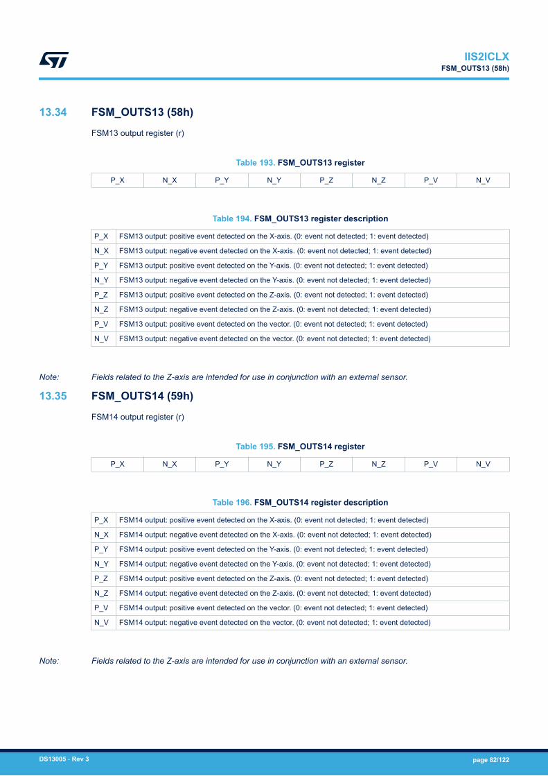
13.34 FSM_OUTS13 (58h)
FSM13 output register (r)
Table 193. FSM_OUTS13 register
P_X N_X P_Y N_Y P_Z N_Z P_V N_V
Table 194. FSM_OUTS13 register description
P_X FSM13 output: positive event detected on the X-axis. (0: event not detected; 1: event detected)
N_X FSM13 output: negative event detected on the X-axis. (0: event not detected; 1: event detected)
P_Y FSM13 output: positive event detected on the Y-axis. (0: event not detected; 1: event detected)
N_Y FSM13 output: negative event detected on the Y-axis. (0: event not detected; 1: event detected)
P_Z FSM13 output: positive event detected on the Z-axis. (0: event not detected; 1: event detected)
N_Z FSM13 output: negative event detected on the Z-axis. (0: event not detected; 1: event detected)
P_V FSM13 output: positive event detected on the vector. (0: event not detected; 1: event detected)
N_V FSM13 output: negative event detected on the vector. (0: event not detected; 1: event detected)
Note: Fields related to the Z-axis are intended for use in conjunction with an external sensor.
13.35 FSM_OUTS14 (59h)
FSM14 output register (r)
Table 195. FSM_OUTS14 register
P_X N_X P_Y N_Y P_Z N_Z P_V N_V
Table 196. FSM_OUTS14 register description
P_X FSM14 output: positive event detected on the X-axis. (0: event not detected; 1: event detected)
N_X FSM14 output: negative event detected on the X-axis. (0: event not detected; 1: event detected)
P_Y FSM14 output: positive event detected on the Y-axis. (0: event not detected; 1: event detected)
N_Y FSM14 output: negative event detected on the Y-axis. (0: event not detected; 1: event detected)
P_Z FSM14 output: positive event detected on the Z-axis. (0: event not detected; 1: event detected)
N_Z FSM14 output: negative event detected on the Z-axis. (0: event not detected; 1: event detected)
P_V FSM14 output: positive event detected on the vector. (0: event not detected; 1: event detected)
N_V FSM14 output: negative event detected on the vector. (0: event not detected; 1: event detected)
Note: Fields related to the Z-axis are intended for use in conjunction with an external sensor.
IIS2ICLXFSM_OUTS13 (58h)
DS13005 - Rev 3 page 82/122
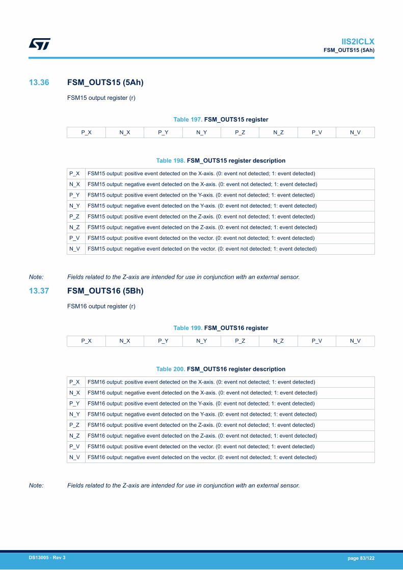
13.36 FSM_OUTS15 (5Ah)
FSM15 output register (r)
Table 197. FSM_OUTS15 register
P_X N_X P_Y N_Y P_Z N_Z P_V N_V
Table 198. FSM_OUTS15 register description
P_X FSM15 output: positive event detected on the X-axis. (0: event not detected; 1: event detected)
N_X FSM15 output: negative event detected on the X-axis. (0: event not detected; 1: event detected)
P_Y FSM15 output: positive event detected on the Y-axis. (0: event not detected; 1: event detected)
N_Y FSM15 output: negative event detected on the Y-axis. (0: event not detected; 1: event detected)
P_Z FSM15 output: positive event detected on the Z-axis. (0: event not detected; 1: event detected)
N_Z FSM15 output: negative event detected on the Z-axis. (0: event not detected; 1: event detected)
P_V FSM15 output: positive event detected on the vector. (0: event not detected; 1: event detected)
N_V FSM15 output: negative event detected on the vector. (0: event not detected; 1: event detected)
Note: Fields related to the Z-axis are intended for use in conjunction with an external sensor.
13.37 FSM_OUTS16 (5Bh)
FSM16 output register (r)
Table 199. FSM_OUTS16 register
P_X N_X P_Y N_Y P_Z N_Z P_V N_V
Table 200. FSM_OUTS16 register description
P_X FSM16 output: positive event detected on the X-axis. (0: event not detected; 1: event detected)
N_X FSM16 output: negative event detected on the X-axis. (0: event not detected; 1: event detected)
P_Y FSM16 output: positive event detected on the Y-axis. (0: event not detected; 1: event detected)
N_Y FSM16 output: negative event detected on the Y-axis. (0: event not detected; 1: event detected)
P_Z FSM16 output: positive event detected on the Z-axis. (0: event not detected; 1: event detected)
N_Z FSM16 output: negative event detected on the Z-axis. (0: event not detected; 1: event detected)
P_V FSM16 output: positive event detected on the vector. (0: event not detected; 1: event detected)
N_V FSM16 output: negative event detected on the vector. (0: event not detected; 1: event detected)
Note: Fields related to the Z-axis are intended for use in conjunction with an external sensor.
IIS2ICLXFSM_OUTS15 (5Ah)
DS13005 - Rev 3 page 83/122
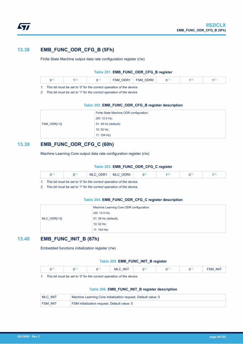
13.38 EMB_FUNC_ODR_CFG_B (5Fh)
Finite State Machine output data rate configuration register (r/w)
Table 201. EMB_FUNC_ODR_CFG_B register
0(1) 1(2) 0(1) FSM_ODR1 FSM_ODR0 0(1) 1(2) 1(2)
1. This bit must be set to '0' for the correct operation of the device.2. This bit must be set to '1' for the correct operation of the device
Table 202. EMB_FUNC_ODR_CFG_B register description
FSM_ODR[1:0]
Finite State Machine ODR configuration:
(00: 12.5 Hz;
01: 26 Hz (default);
10: 52 Hz;
11: 104 Hz)
13.39 EMB_FUNC_ODR_CFG_C (60h)
Machine Learning Core output data rate configuration register (r/w)
Table 203. EMB_FUNC_ODR_CFG_C register
0(1) 0(1) MLC_ODR1 MLC_ODR0 0(1) 1(2) 0(1) 1(2)
1. This bit must be set to '0' for the correct operation of the device.2. This bit must be set to '1' for the correct operation of the device.
Table 204. EMB_FUNC_ODR_CFG_C register description
MLC_ODR[1:0]
Machine Learning Core ODR configuration:
(00: 12.5 Hz;
01: 26 Hz (default);
10: 52 Hz;
11: 104 Hz)
13.40 EMB_FUNC_INIT_B (67h)
Embedded functions initialization register (r/w)
Table 205. EMB_FUNC_INIT_B register
0(1) 0(1) 0(1) MLC_INIT 0(1) 0(1) 0(1) FSM_INIT
1. This bit must be set to '0' for the correct operation of the device.
Table 206. EMB_FUNC_INIT_B register description
MLC_INIT Machine Learning Core initialization request. Default value: 0
FSM_INIT FSM initialization request. Default value: 0
IIS2ICLXEMB_FUNC_ODR_CFG_B (5Fh)
DS13005 - Rev 3 page 84/122

13.41 MLC0_SRC (70h)
Machine Learning Core source register (r)
Table 207. MLC0_SRC register
MLC0_SRC_7
MLC0_SRC_6
MLC0_SRC_5
MLC0_SRC_4
MLC0_SRC_3
MLC0_SRC_2
MLC0_SRC_1
MLC0_SRC_0
Table 208. MLC0_SRC register description
MLC0_SRC_[7:0] Output value of MLC0 decision tree
13.42 MLC1_SRC (71h)
Machine Learning Core source register (r)
Table 209. MLC1_SRC register
MLC1_SRC_7
MLC1_SRC_6
MLC1_SRC_5
MLC1_SRC_4
MLC1_SRC_3
MLC1_SRC_2
MLC1_SRC_1
MLC1_SRC_0
Table 210. MLC1_SRC register description
MLC1_SRC_[7:0] Output value of MLC1 decision tree
13.43 MLC2_SRC (72h)
Machine Learning Core source register (r)
Table 211. MLC2_SRC register
MLC2_SRC_7
MLC2_SRC_6
MLC2_SRC_5
MLC2_SRC_4
MLC2_SRC_3
MLC2_SRC_2
MLC2_SRC_1
MLC2_SRC_0
Table 212. MLC2_SRC register description
MLC2_SRC_[7:0] Output value of MLC2 decision tree
13.44 MLC3_SRC (73h)
Machine Learning Core source register (r)
Table 213. MLC3_SRC register
MLC3_SRC_7
MLC3_SRC_6
MLC3_SRC_5
MLC3_SRC_4
MLC3_SRC_3
MLC3_SRC_2
MLC3_SRC_1
MLC3_SRC_0
Table 214. MLC3_SRC register description
MLC3_SRC_[7:0] Output value of MLC3 decision tree
IIS2ICLXMLC0_SRC (70h)
DS13005 - Rev 3 page 85/122

13.45 MLC4_SRC (74h)
Machine Learning Core source register (r)
Table 215. MLC4_SRC register
MLC4_SRC_7
MLC4_SRC_6
MLC4_SRC_5
MLC4_SRC_4
MLC4_SRC_3
MLC4_SRC_2
MLC4_SRC_1
MLC4_SRC_0
Table 216. MLC4_SRC register description
MLC4_SRC_[7:0] Output value of MLC4 decision tree
13.46 MLC5_SRC (75h)
Machine Learning Core source register (r)
Table 217. MLC5_SRC register
MLC5_SRC_7
MLC5_SRC_6
MLC5_SRC_5
MLC5_SRC_4
MLC5_SRC_3
MLC5_SRC_2
MLC5_SRC_1
MLC5_SRC_0
Table 218. MLC5_SRC register description
MLC5_SRC_[7:0] Output value of MLC5 decision tree
13.47 MLC6_SRC (76h)
Machine Learning Core source register (r)
Table 219. MLC6_SRC register
MLC6_SRC_7
MLC6_SRC_6
MLC6_SRC_5
MLC6_SRC_4
MLC6_SRC_3
MLC6_SRC_2
MLC6_SRC_1
MLC6_SRC_0
Table 220. MLC6_SRC register description
MLC6_SRC_[7:0] Output value of MLC6 decision tree
13.48 MLC7_SRC (77h)
Machine Learning Core source register (r)
Table 221. MLC7_SRC register
MLC7_SRC_7
MLC7_SRC_6
MLC7_SRC_5
MLC7_SRC_4
MLC7_SRC_3
MLC7_SRC_2
MLC7_SRC_1
MLC7_SRC_0
Table 222. MLC7_SRC register description
MLC7_SRC_[7:0] Output value of MLC7 decision tree
IIS2ICLXMLC4_SRC (74h)
DS13005 - Rev 3 page 86/122

14 Embedded advanced features
The following table provides a list of the registers for the embedded advanced features page 1. These registersare accessible when PAGE_SEL[3:0] are set to 0001 in PAGE_SEL (02h).
Table 223. Register address map - embedded advanced features page 1
Name TypeRegister address
Default CommentHex Binary
FSM_LC_TIMEOUT_L RW 7A 01111010 00000000
FSM_LC_TIMEOUT_H RW 7B 01111011 00000000
FSM_PROGRAMS RW 7C 01111100 00000000
FSM_START_ADD_L RW 7E 01111110 00000000
FSM_START_ADD_H RW 7F 01111111 00000000
Registers marked as Reserved must not be changed. Writing to those registers may cause permanent damage tothe device.The content of the registers that are loaded at boot should not be changed. They contain the factory calibrationvalues. Their content is automatically restored when the device is powered up.Write procedure example:Example: write value 01h register at address 7Ch (FSM_PROGRAMS) in Page 1
1. Write bit FUNC_CFG_EN = 1 in FUNC_CFG_ACCESS (01h) // Enable access to embedded functions registers
2. Write bit PAGE_WRITE = 1 in PAGE_RW (17h) register // Select write operation mode
3. Write 0001 in PAGE_SEL[3:0] field of register PAGE_SEL (02h) // Select page 1
4. Write 7Ch in PAGE_ADDR register (08h) // Set address
5. Write 06h in PAGE_DATA register (09h) // Set value to be written
6. Write bit PAGE_WRITE = 0 in PAGE_RW (17h) register // Write operation disabled
7. Write bit FUNC_CFG_EN = 0 in FUNC_CFG_ACCESS (01h) // Disable access to embedded functions registers
Read procedure example:Example: read value of register at address 7Ch (FSM_PROGRAMS) in Page 1
1. Write bit FUNC_CFG_EN = 1 in FUNC_CFG_ACCESS (01h) // Enable access to embedded functions registers
2. Write bit PAGE_READ = 1 in PAGE_RW (17h) register // Select read operation mode
3. Write 0001 in PAGE_SEL[3:0] field of register PAGE_SEL (02h) // Select page 1
4. Write 7Ch in PAGE_ADDR register (08h) // Set address
5. Read value of PAGE_DATA register (09h) // Get register value
6. Write bit PAGE_READ = 0 in PAGE_RW (17h) register // Read operation disabled
7. Write bit FUNC_CFG_EN = 0 in FUNC_CFG_ACCESS (01h) // Disable access to embedded functions registers
IIS2ICLXEmbedded advanced features
DS13005 - Rev 3 page 87/122
Note: Steps 1 and 2 of both procedures are intended to be performed at the beginning of the procedure. Steps 6and 7 of both procedures are intended to be performed at the end of the procedure. If the procedure involvesmultiple operations, only steps 3, 4 and 5 must be repeated for each operation. If, in particular, the multipleoperations involve consecutive registers, only step 5 can be performed.
IIS2ICLXEmbedded advanced features
DS13005 - Rev 3 page 88/122
15 Embedded advanced features register description
15.1 Page 1 - Embedded advanced features registers
15.1.1 FSM_LC_TIMEOUT_L (7Ah) and FSM_LC_TIMEOUT_H (7Bh)FSM long counter timeout register (r/w).The long counter timeout value is an unsigned integer value (16-bit format). When the long counter value reachesthis value, the FSM generates an interrupt.
Table 224. FSM_LC_TIMEOUT_L register
FSM_LC_TIMEOUT7
FSM_LC_TIMEOUT6
FSM_LC_TIMEOUT5
FSM_LC_TIMEOUT4
FSM_LC_TIMEOUT3
FSM_LC_TIMEOUT2
FSM_LC_TIMEOUT1
FSM_LC_TIMEOUT0
Table 225. FSM_LC_TIMEOUT_L register description
FSM_LC_TIMEOUT[7:0] FSM long counter timeout value (LSbyte). Default value: 00000000
Table 226. FSM_LC_TIMEOUT_H register
FSM_LC_TIMEOUT15
FSM_LC_TIMEOUT14
FSM_LC_TIMEOUT13
FSM_LC_TIMEOUT12
FSM_LC_TIMEOUT11
FSM_LC_TIMEOUT10
FSM_LC_TIMEOUT9
FSM_LC_TIMEOUT8
Table 227. FSM_LC_TIMEOUT_H register description
FSM_LC_TIMEOUT[15:8] FSM long counter timeout value (MSbyte). Default value: 00000000
15.1.2 FSM_PROGRAMS (7Ch)FSM number of programs register (r/w)
Table 228. FSM_PROGRAMS register
FSM_N_PROG7
FSM_N_PROG6
FSM_N_PROG5
FSM_N_PROG4
FSM_N_PROG3
FSM_N_PROG2
FSM_N_PROG1
FSM_N_PROG0
Table 229. FSM_PROGRAMS register description
FSM_N_PROG[7:0] Number of FSM programs; must be less than or equal to 16. Default value: 00000000
IIS2ICLXEmbedded advanced features register description
DS13005 - Rev 3 page 89/122

15.1.3 FSM_START_ADD_L (7Eh) and FSM_START_ADD_H (7Fh)FSM start address register (r/w). First available address is 0x033C.
Table 230. FSM_START_ADD_L register
FSM_START7
FSM_START6
FSM_START5
FSM_START4
FSM_START3
FSM_START2
FSM_START1
FSM_START0
Table 231. FSM_START_ADD_L register description
FSM_START[7:0] FSM start address value (LSbyte). Default value: 00000000
Table 232. FSM_START_ADD_H register
FSM_START15
FSM_START14
FSM_START13
FSM_START12
FSM_START11
FSM_START10
FSM_START9
FSM_START8
Table 233. FSM_START_ADD_H register description
FSM_START[15:8] FSM start address value (MSbyte). Default value: 00000000
IIS2ICLXPage 1 - Embedded advanced features registers
DS13005 - Rev 3 page 90/122

16 Sensor hub register map
The table given below provides a list of the registers for the sensor hub functions available in the device and thecorresponding addresses. The sensor hub registers are accessible when bit SHUB_REG_ACCESS is set to '1' inFUNC_CFG_ACCESS (01h).
Table 234. Registers address map
Name TypeRegister address
Default CommentHex Binary
SENSOR_HUB_1 R 02 00000010 output
SENSOR_HUB_2 R 03 00000011 output
SENSOR_HUB_3 R 04 00000100 output
SENSOR_HUB_4 R 05 00000101 output
SENSOR_HUB_5 R 06 00000110 output
SENSOR_HUB_6 R 07 00000111 output
SENSOR_HUB_7 R 08 00001000 output
SENSOR_HUB_8 R 09 00001001 output
SENSOR_HUB_9 R 0A 00001010 output
SENSOR_HUB_10 R 0B 00001011 output
SENSOR_HUB_11 R 0C 00001100 output
SENSOR_HUB_12 R 0D 00001101 output
SENSOR_HUB_13 R 0E 00001110 output
SENSOR_HUB_14 R 0F 00001111 output
SENSOR_HUB_15 R 10 00010000 output
SENSOR_HUB_16 R 11 00010001 output
SENSOR_HUB_17 R 12 00010010 output
SENSOR_HUB_18 R 13 00010011 output
MASTER_CONFIG RW 14 00010100 00000000
SLV0_ADD RW 15 00010101 00000000
SLV0_SUBADD RW 16 00010110 00000000
SLV0_CONFIG RW 17 00010111 00000000
SLV1_ADD RW 18 00011000 00000000
SLV1_SUBADD RW 19 00011001 00000000
SLV1_CONFIG RW 1A 00011010 00000000
SLV2_ADD RW 1B 00011011 00000000
SLV2_SUBADD RW 1C 00011100 00000000
SLV2_CONFIG RW 1D 00011101 00000000
SLV3_ADD RW 1E 00011110 00000000
SLV3_SUBADD RW 1F 00011111 00000000
SLV3_CONFIG RW 20 00100000 00000000
DATAWRITE_SLV0 RW 21 00100001 00000000
STATUS_MASTER R 22 00100010 output
IIS2ICLXSensor hub register map
DS13005 - Rev 3 page 91/122
Registers marked as Reserved must not be changed. Writing to those registers may cause permanent damage tothe device.The content of the registers that are loaded at boot should not be changed. They contain the factory calibrationvalues. Their content is automatically restored when the device is powered up.
IIS2ICLXSensor hub register map
DS13005 - Rev 3 page 92/122

17 Sensor hub register description
17.1 SENSOR_HUB_1 (02h)
Sensor hub output register (r)First byte associated to external sensors. The content of the register is consistent with the SLAVEx_CONFIGnumber of read operation configurations (for external sensors from x = 0 to x = 3).
Table 235. SENSOR_HUB_1 register
SensorHub1_7
SensorHub1_6
SensorHub1_5
SensorHub1_4
SensorHub1_3
SensorHub1_2
SensorHub1_1
SensorHub1_0
Table 236. SENSOR_HUB_1 register description
SensorHub1[7:0] First byte associated to external sensors
17.2 SENSOR_HUB_2 (03h)
Sensor hub output register (r)Second byte associated to external sensors. The content of the register is consistent with the SLAVEx_CONFIGnumber of read operation configurations (for external sensors from x = 0 to x = 3).
Table 237. SENSOR_HUB_2 register
SensorHub2_7
SensorHub2_6
SensorHub2_5
SensorHub2_4
SensorHub2_3
SensorHub2_2
SensorHub2_1
SensorHub2_0
Table 238. SENSOR_HUB_2 register description
SensorHub2[7:0] Second byte associated to external sensors
17.3 SENSOR_HUB_3 (04h)
Sensor hub output register (r)Third byte associated to external sensors. The content of the register is consistent with the SLAVEx_CONFIGnumber of read operation configurations (for external sensors from x = 0 to x = 3).
Table 239. SENSOR_HUB_3 register
SensorHub3_7
SensorHub3_6
SensorHub3_5
SensorHub3_4
SensorHub3_3
SensorHub3_2
SensorHub3_1
SensorHub3_0
Table 240. SENSOR_HUB_3 register description
SensorHub3[7:0] Third byte associated to external sensors
IIS2ICLXSensor hub register description
DS13005 - Rev 3 page 93/122
17.4 SENSOR_HUB_4 (05h)
Sensor hub output register (r)Fourth byte associated to external sensors. The content of the register is consistent with the SLAVEx_CONFIGnumber of read operation configurations (for external sensors from x = 0 to x = 3).
Table 241. SENSOR_HUB_4 register
SensorHub4_7
SensorHub4_6
SensorHub4_5
SensorHub4_4
SensorHub4_3
SensorHub4_2
SensorHub4_1
SensorHub4_0
Table 242. SENSOR_HUB_4 register description
SensorHub4[7:0] Fourth byte associated to external sensors
17.5 SENSOR_HUB_5 (06h)
Sensor hub output register (r)Fifth byte associated to external sensors. The content of the register is consistent with the SLAVEx_CONFIGnumber of read operation configurations (for external sensors from x = 0 to x = 3).
Table 243. SENSOR_HUB_5 register
SensorHub5_7
SensorHub5_6
SensorHub5_5
SensorHub5_4
SensorHub5_3
SensorHub5_2
SensorHub5_1
SensorHub5_0
Table 244. SENSOR_HUB_5 register description
SensorHub5[7:0] Fifth byte associated to external sensors
17.6 SENSOR_HUB_6 (07h)
Sensor hub output register (r)Sixth byte associated to external sensors. The content of the register is consistent with the SLAVEx_CONFIGnumber of read operation configurations (for external sensors from x = 0 to x = 3).
Table 245. SENSOR_HUB_6 register
SensorHub6_7
SensorHub6_6
SensorHub6_5
SensorHub6_4
SensorHub6_3
SensorHub6_2
SensorHub6_1
SensorHub6_0
Table 246. SENSOR_HUB_6 register description
SensorHub6[7:0] Sixth byte associated to external sensors
IIS2ICLXSENSOR_HUB_4 (05h)
DS13005 - Rev 3 page 94/122
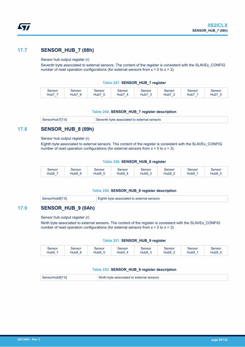
17.7 SENSOR_HUB_7 (08h)
Sensor hub output register (r)Seventh byte associated to external sensors. The content of the register is consistent with the SLAVEx_CONFIGnumber of read operation configurations (for external sensors from x = 0 to x = 3).
Table 247. SENSOR_HUB_7 register
SensorHub7_7
SensorHub7_6
SensorHub7_5
SensorHub7_4
SensorHub7_3
SensorHub7_2
SensorHub7_1
SensorHub7_0
Table 248. SENSOR_HUB_7 register description
SensorHub7[7:0] Seventh byte associated to external sensors
17.8 SENSOR_HUB_8 (09h)
Sensor hub output register (r)Eighth byte associated to external sensors. The content of the register is consistent with the SLAVEx_CONFIGnumber of read operation configurations (for external sensors from x = 0 to x = 3).
Table 249. SENSOR_HUB_8 register
SensorHub8_7
SensorHub8_6
SensorHub8_5
SensorHub8_4
SensorHub8_3
SensorHub8_2
SensorHub8_1
SensorHub8_0
Table 250. SENSOR_HUB_8 register description
SensorHub8[7:0] Eighth byte associated to external sensors
17.9 SENSOR_HUB_9 (0Ah)
Sensor hub output register (r)Ninth byte associated to external sensors. The content of the register is consistent with the SLAVEx_CONFIGnumber of read operation configurations (for external sensors from x = 0 to x = 3).
Table 251. SENSOR_HUB_9 register
SensorHub9_7
SensorHub9_6
SensorHub9_5
SensorHub9_4
SensorHub9_3
SensorHub9_2
SensorHub9_1
SensorHub9_0
Table 252. SENSOR_HUB_9 register description
SensorHub9[7:0] Ninth byte associated to external sensors
IIS2ICLXSENSOR_HUB_7 (08h)
DS13005 - Rev 3 page 95/122
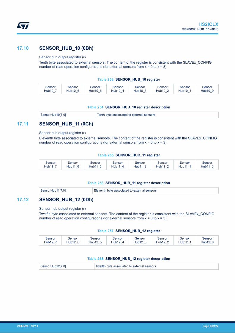
17.10 SENSOR_HUB_10 (0Bh)
Sensor hub output register (r)Tenth byte associated to external sensors. The content of the register is consistent with the SLAVEx_CONFIGnumber of read operation configurations (for external sensors from x = 0 to x = 3).
Table 253. SENSOR_HUB_10 register
SensorHub10_7
SensorHub10_6
SensorHub10_5
SensorHub10_4
SensorHub10_3
SensorHub10_2
SensorHub10_1
SensorHub10_0
Table 254. SENSOR_HUB_10 register description
SensorHub10[7:0] Tenth byte associated to external sensors
17.11 SENSOR_HUB_11 (0Ch)
Sensor hub output register (r)Eleventh byte associated to external sensors. The content of the register is consistent with the SLAVEx_CONFIGnumber of read operation configurations (for external sensors from x = 0 to x = 3).
Table 255. SENSOR_HUB_11 register
SensorHub11_7
SensorHub11_6
SensorHub11_5
SensorHub11_4
SensorHub11_3
SensorHub11_2
SensorHub11_1
SensorHub11_0
Table 256. SENSOR_HUB_11 register description
SensorHub11[7:0] Eleventh byte associated to external sensors
17.12 SENSOR_HUB_12 (0Dh)
Sensor hub output register (r)Twelfth byte associated to external sensors. The content of the register is consistent with the SLAVEx_CONFIGnumber of read operation configurations (for external sensors from x = 0 to x = 3).
Table 257. SENSOR_HUB_12 register
SensorHub12_7
SensorHub12_6
SensorHub12_5
SensorHub12_4
SensorHub12_3
SensorHub12_2
SensorHub12_1
SensorHub12_0
Table 258. SENSOR_HUB_12 register description
SensorHub12[7:0] Twelfth byte associated to external sensors
IIS2ICLXSENSOR_HUB_10 (0Bh)
DS13005 - Rev 3 page 96/122
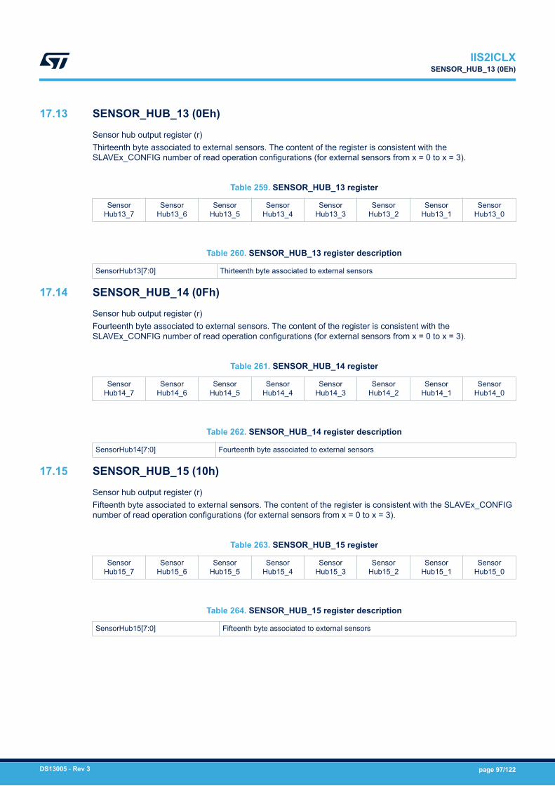
17.13 SENSOR_HUB_13 (0Eh)
Sensor hub output register (r)Thirteenth byte associated to external sensors. The content of the register is consistent with theSLAVEx_CONFIG number of read operation configurations (for external sensors from x = 0 to x = 3).
Table 259. SENSOR_HUB_13 register
SensorHub13_7
SensorHub13_6
SensorHub13_5
SensorHub13_4
SensorHub13_3
SensorHub13_2
SensorHub13_1
SensorHub13_0
Table 260. SENSOR_HUB_13 register description
SensorHub13[7:0] Thirteenth byte associated to external sensors
17.14 SENSOR_HUB_14 (0Fh)
Sensor hub output register (r)Fourteenth byte associated to external sensors. The content of the register is consistent with theSLAVEx_CONFIG number of read operation configurations (for external sensors from x = 0 to x = 3).
Table 261. SENSOR_HUB_14 register
SensorHub14_7
SensorHub14_6
SensorHub14_5
SensorHub14_4
SensorHub14_3
SensorHub14_2
SensorHub14_1
SensorHub14_0
Table 262. SENSOR_HUB_14 register description
SensorHub14[7:0] Fourteenth byte associated to external sensors
17.15 SENSOR_HUB_15 (10h)
Sensor hub output register (r)Fifteenth byte associated to external sensors. The content of the register is consistent with the SLAVEx_CONFIGnumber of read operation configurations (for external sensors from x = 0 to x = 3).
Table 263. SENSOR_HUB_15 register
SensorHub15_7
SensorHub15_6
SensorHub15_5
SensorHub15_4
SensorHub15_3
SensorHub15_2
SensorHub15_1
SensorHub15_0
Table 264. SENSOR_HUB_15 register description
SensorHub15[7:0] Fifteenth byte associated to external sensors
IIS2ICLXSENSOR_HUB_13 (0Eh)
DS13005 - Rev 3 page 97/122

17.16 SENSOR_HUB_16 (11h)
Sensor hub output register (r)Sixteenth byte associated to external sensors. The content of the register is consistent with the SLAVEx_CONFIGnumber of read operation configurations (for external sensors from x = 0 to x = 3).
Table 265. SENSOR_HUB_16 register
SensorHub16_7
SensorHub16_6
SensorHub16_5
SensorHub16_4
SensorHub16_3
SensorHub16_2
SensorHub16_1
SensorHub16_0
Table 266. SENSOR_HUB_16 register description
SensorHub16[7:0] Sixteenth byte associated to external sensors
17.17 SENSOR_HUB_17 (12h)
Sensor hub output register (r)Seventeenth byte associated to external sensors. The content of the register is consistent with theSLAVEx_CONFIG number of read operation configurations (for external sensors from x = 0 to x = 3).
Table 267. SENSOR_HUB_17 register
SensorHub17_7
SensorHub17_6
SensorHub17_5
SensorHub17_4
SensorHub17_3
SensorHub17_2
SensorHub17_1
SensorHub17_0
Table 268. SENSOR_HUB_17 register description
SensorHub17[7:0] Seventeenth byte associated to external sensors
17.18 SENSOR_HUB_18 (13h)
Sensor hub output register (r)Eighteenth byte associated to external sensors. The content of the register is consistent with theSLAVEx_CONFIG number of read operation configurations (for external sensors from x = 0 to x = 3).
Table 269. SENSOR_HUB_18 register
SensorHub18_7
SensorHub18_6
SensorHub18_5
SensorHub18_4
SensorHub18_3
SensorHub18_2
SensorHub18_1
SensorHub18_0
Table 270. SENSOR_HUB_18 register description
SensorHub18[7:0] Eighteenth byte associated to external sensors
IIS2ICLXSENSOR_HUB_16 (11h)
DS13005 - Rev 3 page 98/122

17.19 MASTER_CONFIG (14h)
Master configuration register (r/w)
Table 271. MASTER_CONFIG register
RST_MASTER_REGS
WRITE_ONCE
START_CONFIG
PASS_THROUGH_MODE
SHUB_PU_EN
MASTER_ON
AUX_SENS_ON1
AUX_SENS_ON0
Table 272. MASTER_CONFIG register description
RST_MASTER_REGS Reset Master logic and output registers. Must be set to ‘1’ and then set it to ‘0’. Default value: 0
WRITE_ONCE
Slave 0 write operation is performed only at the first sensor hub cycle.
Default value: 0
(0: write operation for each sensor hub cycle;
1: write operation only for the first sensor hub cycle)
START_CONFIG
Sensor hub trigger signal selection. Default value: 0
(0: sensor hub trigger signal is the accelerometer data-ready;
1: sensor hub trigger signal external from INT2 pin)
PASS_THROUGH_MODE
I²C interface pass-through. Default value: 0
(0: pass-through disabled;
1: pass-through enabled, main I²C line is short-circuited with the auxiliary line)
SHUB_PU_EN
Master I²C pull-up enable. Default value: 0
(0: internal pull-up on auxiliary I²C line disabled;
1: internal pull-up on auxiliary I²C line enabled)
MASTER_ONSensor hub I²C master enable. Default: 0
(0: master I²C of sensor hub disabled; 1: master I²C of sensor hub enabled)
AUX_SENS_ON[1:0]
Number of external sensors to be read by the sensor hub.
(00: one sensor (default);
01: two sensors;
10: three sensors;
11: four sensors)
17.20 SLV0_ADD (15h)
I²C slave address of the first external sensor (Sensor 1) register (r/w)
Table 273. SLV0_ADD register
slave0_add6
slave0_add5
slave0_add4
slave0_add3
slave0_add2
slave0_add1
slave0_add0 rw_0
Table 274. SLV0_ADD register description
slave0_add[6:0] I²C slave address of Sensor1 that can be read by the sensor hub. Default value: 0000000
rw_0Read/write operation on Sensor 1. Default value: 0
(0: write operation; 1: read operation)
IIS2ICLXMASTER_CONFIG (14h)
DS13005 - Rev 3 page 99/122
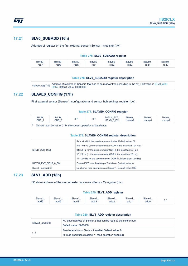
17.21 SLV0_SUBADD (16h)
Address of register on the first external sensor (Sensor 1) register (r/w)
Table 275. SLV0_SUBADD register
slave0_reg7
slave0_reg6
slave0_reg5
slave0_reg4
slave0_reg3
slave0_reg2
slave0_reg1
slave0_reg0
Table 276. SLV0_SUBADD register description
slave0_reg[7:0] Address of register on Sensor1 that has to be read/written according to the rw_0 bit value in SLV0_ADD(15h). Default value: 00000000
17.22 SLAVE0_CONFIG (17h)
First external sensor (Sensor1) configuration and sensor hub settings register (r/w)
Table 277. SLAVE0_CONFIG register
SHUB_ODR_1
SHUB_ODR_0 0(1) 0(1) BATCH_EXT_
SENS_0_ENSlave0_numop2
Slave0_numop1
Slave0_numop0
1. This bit must be set to ‘0’ for the correct operation of the device.
Table 278. SLAVE0_CONFIG register description
SHUB_ODR_[1:0]
Rate at which the master communicates. Default value: 00
(00: 104 Hz (or the accelerometer ODR if it is less than 104 Hz);
01: 52 Hz (or the accelerometer ODR if it is less than 52 Hz);
10: 26 Hz (or the accelerometer ODR if it is less than 26 Hz);
11: 12.5 Hz (or the accelerometer ODR if it is less than 12.5 Hz)
BATCH_EXT_SENS_0_EN Enable FIFO data batching of first slave. Default value: 0
Slave0_numop[2:0] Number of read operations on Sensor 1. Default value: 000
17.23 SLV1_ADD (18h)
I²C slave address of the second external sensor (Sensor 2) register (r/w)
Table 279. SLV1_ADD register
Slave1_add6
Slave1_add5
Slave1_add4
Slave1_add3
Slave1_add2
Slave1_add1
Slave1_add0 r_1
Table 280. SLV1_ADD register description
Slave1_add[6:0]I²C slave address of Sensor 2 that can be read by the sensor hub.
Default value: 0000000
r_1Read operation on Sensor 2 enable. Default value: 0
(0: read operation disabled; 1: read operation enabled)
IIS2ICLXSLV0_SUBADD (16h)
DS13005 - Rev 3 page 100/122
17.24 SLV1_SUBADD (19h)
Address of register on the second external sensor (Sensor 2) register (r/w)
Table 281. SLV1_SUBADD register
Slave1_reg7
Slave1_reg6
Slave1_reg5
Slave1_reg4
Slave1_reg3
Slave1_reg2
Slave1_reg1
Slave1_reg0
Table 282. SLV1_SUBADD register description
Slave1_reg[7:0] Address of register on Sensor 2 that has to be read/written according to the r_1 bit value in SLV1_ADD(18h).
17.25 SLAVE1_CONFIG (1Ah)
Second external sensor (Sensor 2) configuration register (r/w)
Table 283. SLAVE1_CONFIG register
0(1) 0(1) 0(1) 0(1) BATCH_EXT_SENS_1_EN
Slave1_numop2
Slave1_numop1
Slave1_numop0
1. This bit must be set to ‘0’ for the correct operation of the device.
Table 284. SLAVE1_CONFIG register description
BATCH_EXT_SENS_1_EN Enable FIFO data batching of second slave. Default value: 0
Slave1_numop[2:0] Number of read operations on Sensor 2. Default value: 000
17.26 SLV2_ADD (1Bh)
I²C slave address of the third external sensor (Sensor 3) register (r/w)
Table 285. SLV2_ADD register
Slave2_add6
Slave2_add5
Slave2_add4
Slave2_add3
Slave2_add2
Slave2_add1
Slave2_add0 r_2
Table 286. SLV2_ADD register description
Slave2_add[6:0] I²C slave address of Sensor 3 that can be read by the sensor hub.
r_2Read operation on Sensor 3 enable. Default value: 0
(0: read operation disabled; 1: read operation enabled)
IIS2ICLXSLV1_SUBADD (19h)
DS13005 - Rev 3 page 101/122

17.27 SLV2_SUBADD (1Ch)
Address of register on the third external sensor (Sensor 3) register (r/w)
Table 287. SLV2_SUBADD register
Slave2_reg7
Slave2_reg6
Slave2_reg5
Slave2_reg4
Slave2_reg3
Slave2_reg2
Slave2_reg1
Slave2_reg0
Table 288. SLV2_SUBADD register description
Slave2_reg[7:0] Address of register on Sensor 3 that has to be read/written according to the r_2 bit value in SLV2_ADD(1Bh).
17.28 SLAVE2_CONFIG (1Dh)
Third external sensor (Sensor 3) configuration register (r/w)
Table 289. SLAVE2_CONFIG register
0(1) 0(1) 0(1) 0(1) BATCH_EXT_SENS_2_EN
Slave2_numop2
Slave2_numop1
Slave2_numop0
1. This bit must be set to ‘0’ for the correct operation of the device.
Table 290. SLAVE2_CONFIG register description
BATCH_EXT_SENS_2_EN Enable FIFO data batching of third slave. Default value: 0
Slave2_numop[2:0] Number of read operations on Sensor 3. Default value: 000
17.29 SLV3_ADD (1Eh)
I²C slave address of the fourth external sensor (Sensor 4) register (r/w)
Table 291. SLV3_ADD register
Slave3_add6
Slave3_add5
Slave3_add4
Slave3_add3
Slave3_add2
Slave3_add1
Slave3_add0 r_3
Table 292. SLV3_ADD register description
Slave3_add[6:0] I²C slave address of Sensor 4 that can be read by the sensor hub.
r_3Read operation on Sensor 4 enable. Default value: 0
(0: read operation disabled; 1: read operation enabled)
IIS2ICLXSLV2_SUBADD (1Ch)
DS13005 - Rev 3 page 102/122
17.30 SLV3_SUBADD (1Fh)
Address of register on the fourth external sensor (Sensor 4) register (r/w)
Table 293. SLV3_SUBADD register
Slave3_reg7
Slave3_reg6
Slave3_reg5
Slave3_reg4
Slave3_reg3
Slave3_reg2
Slave3_reg1
Slave3_reg0
Table 294. SLV3_SUBADD register description
Slave3_reg[7:0] Address of register on Sensor 4 that has to be read according to the r_3 bit value in SLV3_ADD (1Eh).
17.31 SLAVE3_CONFIG (20h)
Fourth external sensor (Sensor 4) configuration register (r/w)
Table 295. SLAVE3_CONFIG register
0(1) 0(1) 0(1) 0(1) BATCH_EXT_SENS_3_EN
Slave3_numop2
Slave3_numop1
Slave3_numop0
1. This bit must be set to ‘0’ for the correct operation of the device.
Table 296. SLAVE3_CONFIG register description
BATCH_EXT_SENS_3_EN Enable FIFO data batching of fourth slave. Default value: 0
Slave3_numop[2:0] Number of read operations on Sensor 4. Default value: 000
17.32 DATAWRITE_SLV0 (21h)
Data to be written into the slave device register (r/w)
Table 297. DATAWRITE_SLV0 register
Slave0_dataw7
Slave0_dataw6
Slave0_dataw5
Slave0_dataw4
Slave0_dataw3
Slave0_dataw2
Slave0_dataw1
Slave0_dataw0
Table 298. DATAWRITE_SLV0 register description
Slave0_dataw[7:0]Data to be written into the slave 0 device according to the rw_0 bit in register SLV0_ADD (15h).
Default value: 00000000
IIS2ICLXSLV3_SUBADD (1Fh)
DS13005 - Rev 3 page 103/122
17.33 STATUS_MASTER (22h)
Sensor hub source register (r)
Table 299. STATUS_MASTER register
WR_ONCE_DONE
SLAVE3_NACK
SLAVE2_NACK
SLAVE1_NACK
SLAVE0_NACK 0 0 SENS_HUB
_ENDOP
Table 300. STATUS_MASTER register description
WR_ONCE_DONE When the bit WRITE_ONCE in MASTER_CONFIG (14h) is configured as 1, this bit is set to 1 when thewrite operation on slave 0 has been performed and completed. Default value: 0
SLAVE3_NACK This bit is set to 1 if Not acknowledge occurs on slave 3 communication. Default value: 0
SLAVE2_NACK This bit is set to 1 if Not acknowledge occurs on slave 2 communication. Default value: 0
SLAVE1_NACK This bit is set to 1 if Not acknowledge occurs on slave 1 communication. Default value: 0
SLAVE0_NACK This bit is set to 1 if Not acknowledge occurs on slave 0 communication. Default value: 0
SENS_HUB_ENDOP
Sensor hub communication status. Default value: 0
(0: sensor hub communication not concluded;
1: sensor hub communication concluded)
IIS2ICLXSTATUS_MASTER (22h)
DS13005 - Rev 3 page 104/122

18 Soldering information
The LGA package is compliant with the ECOPACK, RoHS and "Green" standard.It is qualified for soldering heat resistance according to JEDEC J-STD-020.Land pattern and soldering recommendations are available at www.st.com/mems.
IIS2ICLXSoldering information
DS13005 - Rev 3 page 105/122
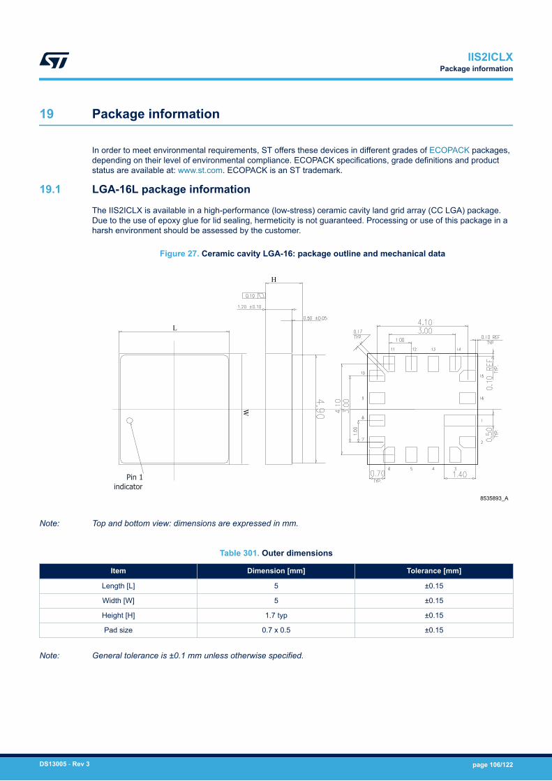
19 Package information
In order to meet environmental requirements, ST offers these devices in different grades of ECOPACK packages,depending on their level of environmental compliance. ECOPACK specifications, grade definitions and productstatus are available at: www.st.com. ECOPACK is an ST trademark.
19.1 LGA-16L package information
The IIS2ICLX is available in a high-performance (low-stress) ceramic cavity land grid array (CC LGA) package.Due to the use of epoxy glue for lid sealing, hermeticity is not guaranteed. Processing or use of this package in aharsh environment should be assessed by the customer.
Figure 27. Ceramic cavity LGA-16: package outline and mechanical data
Pin 1indicator
L
H
W
8535893_A
Note: Top and bottom view: dimensions are expressed in mm.
Table 301. Outer dimensions
Item Dimension [mm] Tolerance [mm]
Length [L] 5 ±0.15
Width [W] 5 ±0.15
Height [H] 1.7 typ ±0.15
Pad size 0.7 x 0.5 ±0.15
Note: General tolerance is ±0.1 mm unless otherwise specified.
IIS2ICLXPackage information
DS13005 - Rev 3 page 106/122
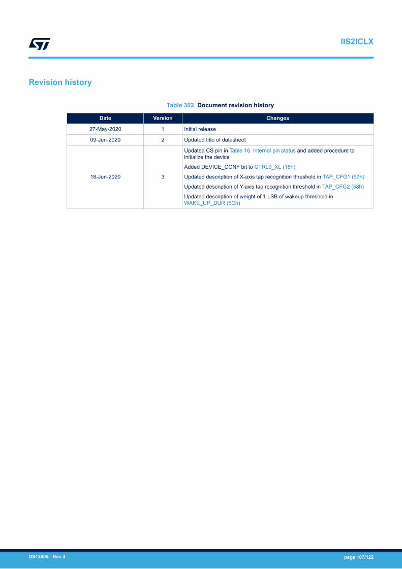
Revision history
Table 302. Document revision history
Date Version Changes
27-May-2020 1 Initial release
09-Jun-2020 2 Updated title of datasheet
18-Jun-2020 3
Updated CS pin in Table 16. Internal pin status and added procedure toinitialize the device
Added DEVICE_CONF bit to CTRL9_XL (18h)
Updated description of X-axis tap recognition threshold in TAP_CFG1 (57h)
Updated description of Y-axis tap recognition threshold in TAP_CFG2 (58h)
Updated description of weight of 1 LSB of wakeup threshold inWAKE_UP_DUR (5Ch)
IIS2ICLX
DS13005 - Rev 3 page 107/122

Contents
1 Overview . . . . . . . . . . . . . . . . . . . . . . . . . . . . . . . . . . . . . . . . . . . . . . . . . . . . . . . . . . . . . . . . . . . . . . . . . .3
2 Embedded low-power features . . . . . . . . . . . . . . . . . . . . . . . . . . . . . . . . . . . . . . . . . . . . . . . . . . . . .4
2.1 Finite State Machine . . . . . . . . . . . . . . . . . . . . . . . . . . . . . . . . . . . . . . . . . . . . . . . . . . . . . . . . . . . . 5
2.2 Machine Learning Core . . . . . . . . . . . . . . . . . . . . . . . . . . . . . . . . . . . . . . . . . . . . . . . . . . . . . . . . . 6
3 Pin description . . . . . . . . . . . . . . . . . . . . . . . . . . . . . . . . . . . . . . . . . . . . . . . . . . . . . . . . . . . . . . . . . . . .7
3.1 Pin connections . . . . . . . . . . . . . . . . . . . . . . . . . . . . . . . . . . . . . . . . . . . . . . . . . . . . . . . . . . . . . . . . 7
4 Module specifications . . . . . . . . . . . . . . . . . . . . . . . . . . . . . . . . . . . . . . . . . . . . . . . . . . . . . . . . . . . . .9
4.1 Mechanical characteristics . . . . . . . . . . . . . . . . . . . . . . . . . . . . . . . . . . . . . . . . . . . . . . . . . . . . . . . 9
4.2 Electrical characteristics. . . . . . . . . . . . . . . . . . . . . . . . . . . . . . . . . . . . . . . . . . . . . . . . . . . . . . . . 10
4.3 Temperature sensor characteristics . . . . . . . . . . . . . . . . . . . . . . . . . . . . . . . . . . . . . . . . . . . . . . 10
4.4 Communication interface characteristics . . . . . . . . . . . . . . . . . . . . . . . . . . . . . . . . . . . . . . . . . . 11
4.4.1 SPI - serial peripheral interface . . . . . . . . . . . . . . . . . . . . . . . . . . . . . . . . . . . . . . . . . . . . . 11
4.4.2 I²C - inter-IC control interface . . . . . . . . . . . . . . . . . . . . . . . . . . . . . . . . . . . . . . . . . . . . . . 12
4.5 Absolute maximum ratings. . . . . . . . . . . . . . . . . . . . . . . . . . . . . . . . . . . . . . . . . . . . . . . . . . . . . . 13
5 Digital interfaces . . . . . . . . . . . . . . . . . . . . . . . . . . . . . . . . . . . . . . . . . . . . . . . . . . . . . . . . . . . . . . . . .14
5.1 I²C/SPI interface . . . . . . . . . . . . . . . . . . . . . . . . . . . . . . . . . . . . . . . . . . . . . . . . . . . . . . . . . . . . . . 14
5.2 I²C serial interface . . . . . . . . . . . . . . . . . . . . . . . . . . . . . . . . . . . . . . . . . . . . . . . . . . . . . . . . . . . . . 14
5.2.1 I²C operation . . . . . . . . . . . . . . . . . . . . . . . . . . . . . . . . . . . . . . . . . . . . . . . . . . . . . . . . . . . 15
5.3 SPI bus interface. . . . . . . . . . . . . . . . . . . . . . . . . . . . . . . . . . . . . . . . . . . . . . . . . . . . . . . . . . . . . . 17
5.3.1 SPI read . . . . . . . . . . . . . . . . . . . . . . . . . . . . . . . . . . . . . . . . . . . . . . . . . . . . . . . . . . . . . . 18
5.3.2 SPI write . . . . . . . . . . . . . . . . . . . . . . . . . . . . . . . . . . . . . . . . . . . . . . . . . . . . . . . . . . . . . . 19
5.3.3 SPI read in 3-wire mode . . . . . . . . . . . . . . . . . . . . . . . . . . . . . . . . . . . . . . . . . . . . . . . . . . 19
5.4 Master I²C interface . . . . . . . . . . . . . . . . . . . . . . . . . . . . . . . . . . . . . . . . . . . . . . . . . . . . . . . . . . . 20
6 Functionality . . . . . . . . . . . . . . . . . . . . . . . . . . . . . . . . . . . . . . . . . . . . . . . . . . . . . . . . . . . . . . . . . . . . .21
6.1 Block diagram of filters . . . . . . . . . . . . . . . . . . . . . . . . . . . . . . . . . . . . . . . . . . . . . . . . . . . . . . . . . 21
6.1.1 Block diagrams of the accelerometer filters. . . . . . . . . . . . . . . . . . . . . . . . . . . . . . . . . . . . 21
6.2 FIFO . . . . . . . . . . . . . . . . . . . . . . . . . . . . . . . . . . . . . . . . . . . . . . . . . . . . . . . . . . . . . . . . . . . . . . . . 23
6.2.1 Bypass mode . . . . . . . . . . . . . . . . . . . . . . . . . . . . . . . . . . . . . . . . . . . . . . . . . . . . . . . . . . 23
6.2.2 FIFO mode . . . . . . . . . . . . . . . . . . . . . . . . . . . . . . . . . . . . . . . . . . . . . . . . . . . . . . . . . . . . 23
IIS2ICLXContents
DS13005 - Rev 3 page 108/122

6.2.3 Continuous mode . . . . . . . . . . . . . . . . . . . . . . . . . . . . . . . . . . . . . . . . . . . . . . . . . . . . . . . 24
6.2.4 Continuous-to-FIFO mode. . . . . . . . . . . . . . . . . . . . . . . . . . . . . . . . . . . . . . . . . . . . . . . . . 24
6.2.5 Bypass-to-Continuous mode . . . . . . . . . . . . . . . . . . . . . . . . . . . . . . . . . . . . . . . . . . . . . . . 24
6.2.6 Bypass-to-FIFO mode. . . . . . . . . . . . . . . . . . . . . . . . . . . . . . . . . . . . . . . . . . . . . . . . . . . . 24
6.2.7 FIFO reading procedure . . . . . . . . . . . . . . . . . . . . . . . . . . . . . . . . . . . . . . . . . . . . . . . . . . 24
7 Frequency response . . . . . . . . . . . . . . . . . . . . . . . . . . . . . . . . . . . . . . . . . . . . . . . . . . . . . . . . . . . . . .25
8 Typical performance characteristics . . . . . . . . . . . . . . . . . . . . . . . . . . . . . . . . . . . . . . . . . . . . . .26
8.1 Frequency response measurements . . . . . . . . . . . . . . . . . . . . . . . . . . . . . . . . . . . . . . . . . . . . . 26
9 Application hints . . . . . . . . . . . . . . . . . . . . . . . . . . . . . . . . . . . . . . . . . . . . . . . . . . . . . . . . . . . . . . . . .28
9.1 IIS2ICLX electrical connections in Mode 1. . . . . . . . . . . . . . . . . . . . . . . . . . . . . . . . . . . . . . . . . 28
9.2 IIS2ICLX electrical connections in Mode 2. . . . . . . . . . . . . . . . . . . . . . . . . . . . . . . . . . . . . . . . . 29
10 Register map . . . . . . . . . . . . . . . . . . . . . . . . . . . . . . . . . . . . . . . . . . . . . . . . . . . . . . . . . . . . . . . . . . . . .31
11 Register description . . . . . . . . . . . . . . . . . . . . . . . . . . . . . . . . . . . . . . . . . . . . . . . . . . . . . . . . . . . . . .33
11.1 FUNC_CFG_ACCESS (01h) . . . . . . . . . . . . . . . . . . . . . . . . . . . . . . . . . . . . . . . . . . . . . . . . . . . . 33
11.2 PIN_CTRL (02h) . . . . . . . . . . . . . . . . . . . . . . . . . . . . . . . . . . . . . . . . . . . . . . . . . . . . . . . . . . . . . . 33
11.3 FIFO_CTRL1 (07h) . . . . . . . . . . . . . . . . . . . . . . . . . . . . . . . . . . . . . . . . . . . . . . . . . . . . . . . . . . . . 34
11.4 FIFO_CTRL2 (08h) . . . . . . . . . . . . . . . . . . . . . . . . . . . . . . . . . . . . . . . . . . . . . . . . . . . . . . . . . . . . 34
11.5 FIFO_CTRL3 (09h) . . . . . . . . . . . . . . . . . . . . . . . . . . . . . . . . . . . . . . . . . . . . . . . . . . . . . . . . . . . . 35
11.6 FIFO_CTRL4 (0Ah). . . . . . . . . . . . . . . . . . . . . . . . . . . . . . . . . . . . . . . . . . . . . . . . . . . . . . . . . . . . 36
11.7 COUNTER_BDR_REG1 (0Bh) . . . . . . . . . . . . . . . . . . . . . . . . . . . . . . . . . . . . . . . . . . . . . . . . . . 37
11.8 COUNTER_BDR_REG2 (0Ch) . . . . . . . . . . . . . . . . . . . . . . . . . . . . . . . . . . . . . . . . . . . . . . . . . . 37
11.9 INT1_CTRL (0Dh) . . . . . . . . . . . . . . . . . . . . . . . . . . . . . . . . . . . . . . . . . . . . . . . . . . . . . . . . . . . . . 38
11.10 INT2_CTRL (0Eh) . . . . . . . . . . . . . . . . . . . . . . . . . . . . . . . . . . . . . . . . . . . . . . . . . . . . . . . . . . . . . 38
11.11 WHO_AM_I (0Fh) . . . . . . . . . . . . . . . . . . . . . . . . . . . . . . . . . . . . . . . . . . . . . . . . . . . . . . . . . . . . . 38
11.12 CTRL1_XL (10h) . . . . . . . . . . . . . . . . . . . . . . . . . . . . . . . . . . . . . . . . . . . . . . . . . . . . . . . . . . . . . . 39
11.13 CTRL3_C (12h) . . . . . . . . . . . . . . . . . . . . . . . . . . . . . . . . . . . . . . . . . . . . . . . . . . . . . . . . . . . . . . . 40
11.14 CTRL4_C (13h) . . . . . . . . . . . . . . . . . . . . . . . . . . . . . . . . . . . . . . . . . . . . . . . . . . . . . . . . . . . . . . . 41
11.15 CTRL5_C (14h) . . . . . . . . . . . . . . . . . . . . . . . . . . . . . . . . . . . . . . . . . . . . . . . . . . . . . . . . . . . . . . . 41
11.16 CTRL6_C (15h) . . . . . . . . . . . . . . . . . . . . . . . . . . . . . . . . . . . . . . . . . . . . . . . . . . . . . . . . . . . . . . . 42
11.17 CTRL7_XL (16h) . . . . . . . . . . . . . . . . . . . . . . . . . . . . . . . . . . . . . . . . . . . . . . . . . . . . . . . . . . . . . . 42
IIS2ICLXContents
DS13005 - Rev 3 page 109/122

11.18 CTRL8_XL (17h) . . . . . . . . . . . . . . . . . . . . . . . . . . . . . . . . . . . . . . . . . . . . . . . . . . . . . . . . . . . . . . 43
11.19 CTRL9_XL (18h) . . . . . . . . . . . . . . . . . . . . . . . . . . . . . . . . . . . . . . . . . . . . . . . . . . . . . . . . . . . . . . 44
11.20 CTRL10_C (19h) . . . . . . . . . . . . . . . . . . . . . . . . . . . . . . . . . . . . . . . . . . . . . . . . . . . . . . . . . . . . . . 44
11.21 ALL_INT_SRC (1Ah) . . . . . . . . . . . . . . . . . . . . . . . . . . . . . . . . . . . . . . . . . . . . . . . . . . . . . . . . . . 45
11.22 WAKE_UP_SRC (1Bh). . . . . . . . . . . . . . . . . . . . . . . . . . . . . . . . . . . . . . . . . . . . . . . . . . . . . . . . . 45
11.23 TAP_SRC (1Ch) . . . . . . . . . . . . . . . . . . . . . . . . . . . . . . . . . . . . . . . . . . . . . . . . . . . . . . . . . . . . . . 46
11.24 DEN_SRC (1Dh) . . . . . . . . . . . . . . . . . . . . . . . . . . . . . . . . . . . . . . . . . . . . . . . . . . . . . . . . . . . . . . 46
11.25 STATUS_REG (1Eh). . . . . . . . . . . . . . . . . . . . . . . . . . . . . . . . . . . . . . . . . . . . . . . . . . . . . . . . . . . 47
11.26 OUT_TEMP_L (20h), OUT_TEMP_H (21h). . . . . . . . . . . . . . . . . . . . . . . . . . . . . . . . . . . . . . . . 47
11.27 OUTX_L_A (28h) and OUTX_H_A (29h) . . . . . . . . . . . . . . . . . . . . . . . . . . . . . . . . . . . . . . . . . . 48
11.28 OUTY_L_A (2Ah) and OUTY_H_A (2Bh) . . . . . . . . . . . . . . . . . . . . . . . . . . . . . . . . . . . . . . . . . 48
11.29 EMB_FUNC_STATUS_MAINPAGE (35h) . . . . . . . . . . . . . . . . . . . . . . . . . . . . . . . . . . . . . . . . . 48
11.30 FSM_STATUS_A_MAINPAGE (36h) . . . . . . . . . . . . . . . . . . . . . . . . . . . . . . . . . . . . . . . . . . . . . 49
11.31 FSM_STATUS_B_MAINPAGE (37h) . . . . . . . . . . . . . . . . . . . . . . . . . . . . . . . . . . . . . . . . . . . . . 49
11.32 MLC_STATUS_MAINPAGE (38h) . . . . . . . . . . . . . . . . . . . . . . . . . . . . . . . . . . . . . . . . . . . . . . . . 50
11.33 STATUS_MASTER_MAINPAGE (39h) . . . . . . . . . . . . . . . . . . . . . . . . . . . . . . . . . . . . . . . . . . . . 50
11.34 FIFO_STATUS1 (3Ah) . . . . . . . . . . . . . . . . . . . . . . . . . . . . . . . . . . . . . . . . . . . . . . . . . . . . . . . . . 51
11.35 FIFO_STATUS2 (3Bh) . . . . . . . . . . . . . . . . . . . . . . . . . . . . . . . . . . . . . . . . . . . . . . . . . . . . . . . . . 51
11.36 TIMESTAMP0 (40h), TIMESTAMP1 (41h), TIMESTAMP2 (42h), and TIMESTAMP3 (43h) 52
11.37 TAP_CFG0 (56h). . . . . . . . . . . . . . . . . . . . . . . . . . . . . . . . . . . . . . . . . . . . . . . . . . . . . . . . . . . . . . 53
11.38 TAP_CFG1 (57h). . . . . . . . . . . . . . . . . . . . . . . . . . . . . . . . . . . . . . . . . . . . . . . . . . . . . . . . . . . . . . 53
11.39 TAP_CFG2 (58h). . . . . . . . . . . . . . . . . . . . . . . . . . . . . . . . . . . . . . . . . . . . . . . . . . . . . . . . . . . . . . 54
11.40 INT_DUR2 (5Ah) . . . . . . . . . . . . . . . . . . . . . . . . . . . . . . . . . . . . . . . . . . . . . . . . . . . . . . . . . . . . . . 54
11.41 WAKE_UP_THS (5Bh) . . . . . . . . . . . . . . . . . . . . . . . . . . . . . . . . . . . . . . . . . . . . . . . . . . . . . . . . . 55
11.42 WAKE_UP_DUR (5Ch) . . . . . . . . . . . . . . . . . . . . . . . . . . . . . . . . . . . . . . . . . . . . . . . . . . . . . . . . 55
11.43 MD1_CFG (5Eh) . . . . . . . . . . . . . . . . . . . . . . . . . . . . . . . . . . . . . . . . . . . . . . . . . . . . . . . . . . . . . . 56
11.44 MD2_CFG (5Fh) . . . . . . . . . . . . . . . . . . . . . . . . . . . . . . . . . . . . . . . . . . . . . . . . . . . . . . . . . . . . . . 57
11.45 INTERNAL_FREQ_FINE (63h) . . . . . . . . . . . . . . . . . . . . . . . . . . . . . . . . . . . . . . . . . . . . . . . . . . 58
11.46 X_OFS_USR (73h) . . . . . . . . . . . . . . . . . . . . . . . . . . . . . . . . . . . . . . . . . . . . . . . . . . . . . . . . . . . . 59
11.47 Y_OFS_USR (74h) . . . . . . . . . . . . . . . . . . . . . . . . . . . . . . . . . . . . . . . . . . . . . . . . . . . . . . . . . . . . 59
IIS2ICLXContents
DS13005 - Rev 3 page 110/122

11.48 FIFO_DATA_OUT_TAG (78h) . . . . . . . . . . . . . . . . . . . . . . . . . . . . . . . . . . . . . . . . . . . . . . . . . . . 60
11.49 FIFO_DATA_OUT_X_L (79h) and FIFO_DATA_OUT_X_H (7Ah) . . . . . . . . . . . . . . . . . . . . . 61
11.50 FIFO_DATA_OUT_Y_L (7Bh) and FIFO_DATA_OUT_Y_H (7Ch) . . . . . . . . . . . . . . . . . . . . . 61
11.51 FIFO_DATA_OUT_Z_L (7Dh) and FIFO_DATA_OUT_Z_H (7Eh) . . . . . . . . . . . . . . . . . . . . . 61
12 Embedded functions register map . . . . . . . . . . . . . . . . . . . . . . . . . . . . . . . . . . . . . . . . . . . . . . . .62
13 Embedded functions register description . . . . . . . . . . . . . . . . . . . . . . . . . . . . . . . . . . . . . . . . .64
13.1 PAGE_SEL (02h) . . . . . . . . . . . . . . . . . . . . . . . . . . . . . . . . . . . . . . . . . . . . . . . . . . . . . . . . . . . . . 64
13.2 EMB_FUNC_EN_B (05h). . . . . . . . . . . . . . . . . . . . . . . . . . . . . . . . . . . . . . . . . . . . . . . . . . . . . . . 64
13.3 PAGE_ADDRESS (08h) . . . . . . . . . . . . . . . . . . . . . . . . . . . . . . . . . . . . . . . . . . . . . . . . . . . . . . . . 64
13.4 PAGE_VALUE (09h) . . . . . . . . . . . . . . . . . . . . . . . . . . . . . . . . . . . . . . . . . . . . . . . . . . . . . . . . . . . 65
13.5 EMB_FUNC_INT1 (0Ah) . . . . . . . . . . . . . . . . . . . . . . . . . . . . . . . . . . . . . . . . . . . . . . . . . . . . . . . 65
13.6 FSM_INT1_A (0Bh) . . . . . . . . . . . . . . . . . . . . . . . . . . . . . . . . . . . . . . . . . . . . . . . . . . . . . . . . . . . 66
13.7 FSM_INT1_B (0Ch) . . . . . . . . . . . . . . . . . . . . . . . . . . . . . . . . . . . . . . . . . . . . . . . . . . . . . . . . . . . 67
13.8 MLC_INT1 (0Dh) . . . . . . . . . . . . . . . . . . . . . . . . . . . . . . . . . . . . . . . . . . . . . . . . . . . . . . . . . . . . . . 68
13.9 EMB_FUNC_INT2 (0Eh) . . . . . . . . . . . . . . . . . . . . . . . . . . . . . . . . . . . . . . . . . . . . . . . . . . . . . . . 68
13.10 FSM_INT2_A (0Fh). . . . . . . . . . . . . . . . . . . . . . . . . . . . . . . . . . . . . . . . . . . . . . . . . . . . . . . . . . . . 69
13.11 FSM_INT2_B (10h). . . . . . . . . . . . . . . . . . . . . . . . . . . . . . . . . . . . . . . . . . . . . . . . . . . . . . . . . . . . 70
13.12 MLC_INT2 (11h) . . . . . . . . . . . . . . . . . . . . . . . . . . . . . . . . . . . . . . . . . . . . . . . . . . . . . . . . . . . . . . 71
13.13 EMB_FUNC_STATUS (12h) . . . . . . . . . . . . . . . . . . . . . . . . . . . . . . . . . . . . . . . . . . . . . . . . . . . . 71
13.14 FSM_STATUS_A (13h). . . . . . . . . . . . . . . . . . . . . . . . . . . . . . . . . . . . . . . . . . . . . . . . . . . . . . . . . 72
13.15 FSM_STATUS_B (14h). . . . . . . . . . . . . . . . . . . . . . . . . . . . . . . . . . . . . . . . . . . . . . . . . . . . . . . . . 72
13.16 MLC_STATUS (15h) . . . . . . . . . . . . . . . . . . . . . . . . . . . . . . . . . . . . . . . . . . . . . . . . . . . . . . . . . . . 73
13.17 PAGE_RW (17h) . . . . . . . . . . . . . . . . . . . . . . . . . . . . . . . . . . . . . . . . . . . . . . . . . . . . . . . . . . . . . . 73
13.18 FSM_ENABLE_A (46h) . . . . . . . . . . . . . . . . . . . . . . . . . . . . . . . . . . . . . . . . . . . . . . . . . . . . . . . . 74
13.19 FSM_ENABLE_B (47h) . . . . . . . . . . . . . . . . . . . . . . . . . . . . . . . . . . . . . . . . . . . . . . . . . . . . . . . . 74
13.20 FSM_LONG_COUNTER_L (48h) and FSM_LONG_COUNTER_H (49h) . . . . . . . . . . . . . . . 75
13.21 FSM_LONG_COUNTER_CLEAR (4Ah) . . . . . . . . . . . . . . . . . . . . . . . . . . . . . . . . . . . . . . . . . . 75
13.22 FSM_OUTS1 (4Ch) . . . . . . . . . . . . . . . . . . . . . . . . . . . . . . . . . . . . . . . . . . . . . . . . . . . . . . . . . . . 76
13.23 FSM_OUTS2 (4Dh) . . . . . . . . . . . . . . . . . . . . . . . . . . . . . . . . . . . . . . . . . . . . . . . . . . . . . . . . . . . 76
13.24 FSM_OUTS3 (4Eh). . . . . . . . . . . . . . . . . . . . . . . . . . . . . . . . . . . . . . . . . . . . . . . . . . . . . . . . . . . . 77
IIS2ICLXContents
DS13005 - Rev 3 page 111/122
13.25 FSM_OUTS4 (4Fh). . . . . . . . . . . . . . . . . . . . . . . . . . . . . . . . . . . . . . . . . . . . . . . . . . . . . . . . . . . . 77
13.26 FSM_OUTS5 (50h) . . . . . . . . . . . . . . . . . . . . . . . . . . . . . . . . . . . . . . . . . . . . . . . . . . . . . . . . . . . . 78
13.27 FSM_OUTS6 (51h) . . . . . . . . . . . . . . . . . . . . . . . . . . . . . . . . . . . . . . . . . . . . . . . . . . . . . . . . . . . . 78
13.28 FSM_OUTS7 (52h) . . . . . . . . . . . . . . . . . . . . . . . . . . . . . . . . . . . . . . . . . . . . . . . . . . . . . . . . . . . . 79
13.29 FSM_OUTS8 (53h) . . . . . . . . . . . . . . . . . . . . . . . . . . . . . . . . . . . . . . . . . . . . . . . . . . . . . . . . . . . . 79
13.30 FSM_OUTS9 (54h) . . . . . . . . . . . . . . . . . . . . . . . . . . . . . . . . . . . . . . . . . . . . . . . . . . . . . . . . . . . . 80
13.31 FSM_OUTS10 (55h) . . . . . . . . . . . . . . . . . . . . . . . . . . . . . . . . . . . . . . . . . . . . . . . . . . . . . . . . . . . 80
13.32 FSM_OUTS11 (56h) . . . . . . . . . . . . . . . . . . . . . . . . . . . . . . . . . . . . . . . . . . . . . . . . . . . . . . . . . . . 81
13.33 FSM_OUTS12 (57h) . . . . . . . . . . . . . . . . . . . . . . . . . . . . . . . . . . . . . . . . . . . . . . . . . . . . . . . . . . . 81
13.34 FSM_OUTS13 (58h) . . . . . . . . . . . . . . . . . . . . . . . . . . . . . . . . . . . . . . . . . . . . . . . . . . . . . . . . . . . 82
13.35 FSM_OUTS14 (59h) . . . . . . . . . . . . . . . . . . . . . . . . . . . . . . . . . . . . . . . . . . . . . . . . . . . . . . . . . . . 82
13.36 FSM_OUTS15 (5Ah) . . . . . . . . . . . . . . . . . . . . . . . . . . . . . . . . . . . . . . . . . . . . . . . . . . . . . . . . . . 83
13.37 FSM_OUTS16 (5Bh) . . . . . . . . . . . . . . . . . . . . . . . . . . . . . . . . . . . . . . . . . . . . . . . . . . . . . . . . . . 83
13.38 EMB_FUNC_ODR_CFG_B (5Fh) . . . . . . . . . . . . . . . . . . . . . . . . . . . . . . . . . . . . . . . . . . . . . . . . 84
13.39 EMB_FUNC_ODR_CFG_C (60h) . . . . . . . . . . . . . . . . . . . . . . . . . . . . . . . . . . . . . . . . . . . . . . . . 84
13.40 EMB_FUNC_INIT_B (67h). . . . . . . . . . . . . . . . . . . . . . . . . . . . . . . . . . . . . . . . . . . . . . . . . . . . . . 84
13.41 MLC0_SRC (70h) . . . . . . . . . . . . . . . . . . . . . . . . . . . . . . . . . . . . . . . . . . . . . . . . . . . . . . . . . . . . . 85
13.42 MLC1_SRC (71h) . . . . . . . . . . . . . . . . . . . . . . . . . . . . . . . . . . . . . . . . . . . . . . . . . . . . . . . . . . . . . 85
13.43 MLC2_SRC (72h) . . . . . . . . . . . . . . . . . . . . . . . . . . . . . . . . . . . . . . . . . . . . . . . . . . . . . . . . . . . . . 85
13.44 MLC3_SRC (73h) . . . . . . . . . . . . . . . . . . . . . . . . . . . . . . . . . . . . . . . . . . . . . . . . . . . . . . . . . . . . . 85
13.45 MLC4_SRC (74h) . . . . . . . . . . . . . . . . . . . . . . . . . . . . . . . . . . . . . . . . . . . . . . . . . . . . . . . . . . . . . 86
13.46 MLC5_SRC (75h) . . . . . . . . . . . . . . . . . . . . . . . . . . . . . . . . . . . . . . . . . . . . . . . . . . . . . . . . . . . . . 86
13.47 MLC6_SRC (76h) . . . . . . . . . . . . . . . . . . . . . . . . . . . . . . . . . . . . . . . . . . . . . . . . . . . . . . . . . . . . . 86
13.48 MLC7_SRC (77h) . . . . . . . . . . . . . . . . . . . . . . . . . . . . . . . . . . . . . . . . . . . . . . . . . . . . . . . . . . . . . 86
14 Embedded advanced features. . . . . . . . . . . . . . . . . . . . . . . . . . . . . . . . . . . . . . . . . . . . . . . . . . . . .87
15 Embedded advanced features register description . . . . . . . . . . . . . . . . . . . . . . . . . . . . . . . .89
15.1 Page 1 - Embedded advanced features registers . . . . . . . . . . . . . . . . . . . . . . . . . . . . . . . . . . . 89
15.1.1 FSM_LC_TIMEOUT_L (7Ah) and FSM_LC_TIMEOUT_H (7Bh). . . . . . . . . . . . . . . . . . . . 89
15.1.2 FSM_PROGRAMS (7Ch) . . . . . . . . . . . . . . . . . . . . . . . . . . . . . . . . . . . . . . . . . . . . . . . . . 89
15.1.3 FSM_START_ADD_L (7Eh) and FSM_START_ADD_H (7Fh) . . . . . . . . . . . . . . . . . . . . . 90
IIS2ICLXContents
DS13005 - Rev 3 page 112/122
16 Sensor hub register map. . . . . . . . . . . . . . . . . . . . . . . . . . . . . . . . . . . . . . . . . . . . . . . . . . . . . . . . . .91
17 Sensor hub register description. . . . . . . . . . . . . . . . . . . . . . . . . . . . . . . . . . . . . . . . . . . . . . . . . . .93
17.1 SENSOR_HUB_1 (02h) . . . . . . . . . . . . . . . . . . . . . . . . . . . . . . . . . . . . . . . . . . . . . . . . . . . . . . . . 93
17.2 SENSOR_HUB_2 (03h) . . . . . . . . . . . . . . . . . . . . . . . . . . . . . . . . . . . . . . . . . . . . . . . . . . . . . . . . 93
17.3 SENSOR_HUB_3 (04h) . . . . . . . . . . . . . . . . . . . . . . . . . . . . . . . . . . . . . . . . . . . . . . . . . . . . . . . . 93
17.4 SENSOR_HUB_4 (05h) . . . . . . . . . . . . . . . . . . . . . . . . . . . . . . . . . . . . . . . . . . . . . . . . . . . . . . . . 94
17.5 SENSOR_HUB_5 (06h) . . . . . . . . . . . . . . . . . . . . . . . . . . . . . . . . . . . . . . . . . . . . . . . . . . . . . . . . 94
17.6 SENSOR_HUB_6 (07h) . . . . . . . . . . . . . . . . . . . . . . . . . . . . . . . . . . . . . . . . . . . . . . . . . . . . . . . . 94
17.7 SENSOR_HUB_7 (08h) . . . . . . . . . . . . . . . . . . . . . . . . . . . . . . . . . . . . . . . . . . . . . . . . . . . . . . . . 95
17.8 SENSOR_HUB_8 (09h) . . . . . . . . . . . . . . . . . . . . . . . . . . . . . . . . . . . . . . . . . . . . . . . . . . . . . . . . 95
17.9 SENSOR_HUB_9 (0Ah). . . . . . . . . . . . . . . . . . . . . . . . . . . . . . . . . . . . . . . . . . . . . . . . . . . . . . . . 95
17.10 SENSOR_HUB_10 (0Bh). . . . . . . . . . . . . . . . . . . . . . . . . . . . . . . . . . . . . . . . . . . . . . . . . . . . . . . 96
17.11 SENSOR_HUB_11 (0Ch). . . . . . . . . . . . . . . . . . . . . . . . . . . . . . . . . . . . . . . . . . . . . . . . . . . . . . . 96
17.12 SENSOR_HUB_12 (0Dh). . . . . . . . . . . . . . . . . . . . . . . . . . . . . . . . . . . . . . . . . . . . . . . . . . . . . . . 96
17.13 SENSOR_HUB_13 (0Eh). . . . . . . . . . . . . . . . . . . . . . . . . . . . . . . . . . . . . . . . . . . . . . . . . . . . . . . 97
17.14 SENSOR_HUB_14 (0Fh) . . . . . . . . . . . . . . . . . . . . . . . . . . . . . . . . . . . . . . . . . . . . . . . . . . . . . . . 97
17.15 SENSOR_HUB_15 (10h) . . . . . . . . . . . . . . . . . . . . . . . . . . . . . . . . . . . . . . . . . . . . . . . . . . . . . . . 97
17.16 SENSOR_HUB_16 (11h) . . . . . . . . . . . . . . . . . . . . . . . . . . . . . . . . . . . . . . . . . . . . . . . . . . . . . . . 98
17.17 SENSOR_HUB_17 (12h) . . . . . . . . . . . . . . . . . . . . . . . . . . . . . . . . . . . . . . . . . . . . . . . . . . . . . . . 98
17.18 SENSOR_HUB_18 (13h) . . . . . . . . . . . . . . . . . . . . . . . . . . . . . . . . . . . . . . . . . . . . . . . . . . . . . . . 98
17.19 MASTER_CONFIG (14h) . . . . . . . . . . . . . . . . . . . . . . . . . . . . . . . . . . . . . . . . . . . . . . . . . . . . . . . 99
17.20 SLV0_ADD (15h). . . . . . . . . . . . . . . . . . . . . . . . . . . . . . . . . . . . . . . . . . . . . . . . . . . . . . . . . . . . . . 99
17.21 SLV0_SUBADD (16h). . . . . . . . . . . . . . . . . . . . . . . . . . . . . . . . . . . . . . . . . . . . . . . . . . . . . . . . .100
17.22 SLAVE0_CONFIG (17h). . . . . . . . . . . . . . . . . . . . . . . . . . . . . . . . . . . . . . . . . . . . . . . . . . . . . . .100
17.23 SLV1_ADD (18h). . . . . . . . . . . . . . . . . . . . . . . . . . . . . . . . . . . . . . . . . . . . . . . . . . . . . . . . . . . . .100
17.24 SLV1_SUBADD (19h). . . . . . . . . . . . . . . . . . . . . . . . . . . . . . . . . . . . . . . . . . . . . . . . . . . . . . . . .101
17.25 SLAVE1_CONFIG (1Ah) . . . . . . . . . . . . . . . . . . . . . . . . . . . . . . . . . . . . . . . . . . . . . . . . . . . . . .101
17.26 SLV2_ADD (1Bh) . . . . . . . . . . . . . . . . . . . . . . . . . . . . . . . . . . . . . . . . . . . . . . . . . . . . . . . . . . . .101
17.27 SLV2_SUBADD (1Ch) . . . . . . . . . . . . . . . . . . . . . . . . . . . . . . . . . . . . . . . . . . . . . . . . . . . . . . . .102
17.28 SLAVE2_CONFIG (1Dh) . . . . . . . . . . . . . . . . . . . . . . . . . . . . . . . . . . . . . . . . . . . . . . . . . . . . . .102
IIS2ICLXContents
DS13005 - Rev 3 page 113/122

17.29 SLV3_ADD (1Eh) . . . . . . . . . . . . . . . . . . . . . . . . . . . . . . . . . . . . . . . . . . . . . . . . . . . . . . . . . . . .102
17.30 SLV3_SUBADD (1Fh). . . . . . . . . . . . . . . . . . . . . . . . . . . . . . . . . . . . . . . . . . . . . . . . . . . . . . . . .103
17.31 SLAVE3_CONFIG (20h). . . . . . . . . . . . . . . . . . . . . . . . . . . . . . . . . . . . . . . . . . . . . . . . . . . . . . .103
17.32 DATAWRITE_SLV0 (21h). . . . . . . . . . . . . . . . . . . . . . . . . . . . . . . . . . . . . . . . . . . . . . . . . . . . . .103
17.33 STATUS_MASTER (22h) . . . . . . . . . . . . . . . . . . . . . . . . . . . . . . . . . . . . . . . . . . . . . . . . . . . . . .104
18 Soldering information. . . . . . . . . . . . . . . . . . . . . . . . . . . . . . . . . . . . . . . . . . . . . . . . . . . . . . . . . . . 105
19 Package information. . . . . . . . . . . . . . . . . . . . . . . . . . . . . . . . . . . . . . . . . . . . . . . . . . . . . . . . . . . . 106
19.1 LGA-16L package information. . . . . . . . . . . . . . . . . . . . . . . . . . . . . . . . . . . . . . . . . . . . . . . . . .106
Revision history . . . . . . . . . . . . . . . . . . . . . . . . . . . . . . . . . . . . . . . . . . . . . . . . . . . . . . . . . . . . . . . . . . . . . 107
Contents . . . . . . . . . . . . . . . . . . . . . . . . . . . . . . . . . . . . . . . . . . . . . . . . . . . . . . . . . . . . . . . . . . . . . . . . . . . . 108
List of tables . . . . . . . . . . . . . . . . . . . . . . . . . . . . . . . . . . . . . . . . . . . . . . . . . . . . . . . . . . . . . . . . . . . . . . . . 115
List of figures. . . . . . . . . . . . . . . . . . . . . . . . . . . . . . . . . . . . . . . . . . . . . . . . . . . . . . . . . . . . . . . . . . . . . . . . 121
IIS2ICLXContents
DS13005 - Rev 3 page 114/122

List of tablesTable 1. Pin description. . . . . . . . . . . . . . . . . . . . . . . . . . . . . . . . . . . . . . . . . . . . . . . . . . . . . . . . . . . . . . . . . . . . . . 8Table 2. Mechanical characteristics . . . . . . . . . . . . . . . . . . . . . . . . . . . . . . . . . . . . . . . . . . . . . . . . . . . . . . . . . . . . . 9Table 3. Electrical characteristics . . . . . . . . . . . . . . . . . . . . . . . . . . . . . . . . . . . . . . . . . . . . . . . . . . . . . . . . . . . . . . 10Table 4. Temperature sensor characteristics . . . . . . . . . . . . . . . . . . . . . . . . . . . . . . . . . . . . . . . . . . . . . . . . . . . . . . 10Table 5. SPI slave timing values (in mode 3) . . . . . . . . . . . . . . . . . . . . . . . . . . . . . . . . . . . . . . . . . . . . . . . . . . . . . . 11Table 6. I²C slave timing values . . . . . . . . . . . . . . . . . . . . . . . . . . . . . . . . . . . . . . . . . . . . . . . . . . . . . . . . . . . . . . . 12Table 7. Absolute maximum ratings . . . . . . . . . . . . . . . . . . . . . . . . . . . . . . . . . . . . . . . . . . . . . . . . . . . . . . . . . . . . 13Table 8. Serial interface pin description . . . . . . . . . . . . . . . . . . . . . . . . . . . . . . . . . . . . . . . . . . . . . . . . . . . . . . . . . . 14Table 9. I²C terminology . . . . . . . . . . . . . . . . . . . . . . . . . . . . . . . . . . . . . . . . . . . . . . . . . . . . . . . . . . . . . . . . . . . . 14Table 10. SAD+Read/Write patterns . . . . . . . . . . . . . . . . . . . . . . . . . . . . . . . . . . . . . . . . . . . . . . . . . . . . . . . . . . . . . 15Table 11. Transfer when master is writing one byte to slave. . . . . . . . . . . . . . . . . . . . . . . . . . . . . . . . . . . . . . . . . . . . . 15Table 12. Transfer when master is writing multiple bytes to slave . . . . . . . . . . . . . . . . . . . . . . . . . . . . . . . . . . . . . . . . . 15Table 13. Transfer when master is receiving (reading) one byte of data from slave . . . . . . . . . . . . . . . . . . . . . . . . . . . . . 15Table 14. Transfer when master is receiving (reading) multiple bytes of data from slave . . . . . . . . . . . . . . . . . . . . . . . . . 15Table 15. Master I²C pin details . . . . . . . . . . . . . . . . . . . . . . . . . . . . . . . . . . . . . . . . . . . . . . . . . . . . . . . . . . . . . . . . 20Table 16. Internal pin status . . . . . . . . . . . . . . . . . . . . . . . . . . . . . . . . . . . . . . . . . . . . . . . . . . . . . . . . . . . . . . . . . . 30Table 17. Registers address map. . . . . . . . . . . . . . . . . . . . . . . . . . . . . . . . . . . . . . . . . . . . . . . . . . . . . . . . . . . . . . . 31Table 18. FUNC_CFG_ACCESS register . . . . . . . . . . . . . . . . . . . . . . . . . . . . . . . . . . . . . . . . . . . . . . . . . . . . . . . . . 33Table 19. FUNC_CFG_ACCESS register description . . . . . . . . . . . . . . . . . . . . . . . . . . . . . . . . . . . . . . . . . . . . . . . . . 33Table 20. PIN_CTRL register. . . . . . . . . . . . . . . . . . . . . . . . . . . . . . . . . . . . . . . . . . . . . . . . . . . . . . . . . . . . . . . . . . 33Table 21. PIN_CTRL register description . . . . . . . . . . . . . . . . . . . . . . . . . . . . . . . . . . . . . . . . . . . . . . . . . . . . . . . . . 33Table 22. FIFO_CTRL1 register . . . . . . . . . . . . . . . . . . . . . . . . . . . . . . . . . . . . . . . . . . . . . . . . . . . . . . . . . . . . . . . . 34Table 23. FIFO_CTRL1 register description. . . . . . . . . . . . . . . . . . . . . . . . . . . . . . . . . . . . . . . . . . . . . . . . . . . . . . . . 34Table 24. FIFO_CTRL2 register . . . . . . . . . . . . . . . . . . . . . . . . . . . . . . . . . . . . . . . . . . . . . . . . . . . . . . . . . . . . . . . . 34Table 25. FIFO_CTRL2 register . . . . . . . . . . . . . . . . . . . . . . . . . . . . . . . . . . . . . . . . . . . . . . . . . . . . . . . . . . . . . . . . 34Table 26. FIFO_CTRL3 register . . . . . . . . . . . . . . . . . . . . . . . . . . . . . . . . . . . . . . . . . . . . . . . . . . . . . . . . . . . . . . . . 35Table 27. FIFO_CTRL3 register description. . . . . . . . . . . . . . . . . . . . . . . . . . . . . . . . . . . . . . . . . . . . . . . . . . . . . . . . 35Table 28. FIFO_CTRL4 register . . . . . . . . . . . . . . . . . . . . . . . . . . . . . . . . . . . . . . . . . . . . . . . . . . . . . . . . . . . . . . . . 36Table 29. FIFO_CTRL4 register description. . . . . . . . . . . . . . . . . . . . . . . . . . . . . . . . . . . . . . . . . . . . . . . . . . . . . . . . 36Table 30. COUNTER_BDR_REG1 register . . . . . . . . . . . . . . . . . . . . . . . . . . . . . . . . . . . . . . . . . . . . . . . . . . . . . . . . 37Table 31. COUNTER_BDR_REG1 register description . . . . . . . . . . . . . . . . . . . . . . . . . . . . . . . . . . . . . . . . . . . . . . . . 37Table 32. COUNTER_BDR_REG2 register description . . . . . . . . . . . . . . . . . . . . . . . . . . . . . . . . . . . . . . . . . . . . . . . . 37Table 33. INT1_CTRL register description. . . . . . . . . . . . . . . . . . . . . . . . . . . . . . . . . . . . . . . . . . . . . . . . . . . . . . . . . 38Table 34. INT2_CTRL register . . . . . . . . . . . . . . . . . . . . . . . . . . . . . . . . . . . . . . . . . . . . . . . . . . . . . . . . . . . . . . . . . 38Table 35. INT2_CTRL register description. . . . . . . . . . . . . . . . . . . . . . . . . . . . . . . . . . . . . . . . . . . . . . . . . . . . . . . . . 38Table 36. Who_Am_I register . . . . . . . . . . . . . . . . . . . . . . . . . . . . . . . . . . . . . . . . . . . . . . . . . . . . . . . . . . . . . . . . . 38Table 37. CTRL1_XL register description . . . . . . . . . . . . . . . . . . . . . . . . . . . . . . . . . . . . . . . . . . . . . . . . . . . . . . . . . 39Table 38. Accelerometer ODR register setting . . . . . . . . . . . . . . . . . . . . . . . . . . . . . . . . . . . . . . . . . . . . . . . . . . . . . . 39Table 39. Accelerometer full-scale selection . . . . . . . . . . . . . . . . . . . . . . . . . . . . . . . . . . . . . . . . . . . . . . . . . . . . . . . 39Table 40. CTRL3_C register . . . . . . . . . . . . . . . . . . . . . . . . . . . . . . . . . . . . . . . . . . . . . . . . . . . . . . . . . . . . . . . . . . 40Table 41. CTRL3_C register description . . . . . . . . . . . . . . . . . . . . . . . . . . . . . . . . . . . . . . . . . . . . . . . . . . . . . . . . . . 40Table 42. CTRL4_C register . . . . . . . . . . . . . . . . . . . . . . . . . . . . . . . . . . . . . . . . . . . . . . . . . . . . . . . . . . . . . . . . . . 41Table 43. CTRL4_C register description . . . . . . . . . . . . . . . . . . . . . . . . . . . . . . . . . . . . . . . . . . . . . . . . . . . . . . . . . . 41Table 44. CTRL5_C register . . . . . . . . . . . . . . . . . . . . . . . . . . . . . . . . . . . . . . . . . . . . . . . . . . . . . . . . . . . . . . . . . . 41Table 45. CTRL5_C register description . . . . . . . . . . . . . . . . . . . . . . . . . . . . . . . . . . . . . . . . . . . . . . . . . . . . . . . . . . 41Table 46. Linear acceleration sensor self-test mode selection . . . . . . . . . . . . . . . . . . . . . . . . . . . . . . . . . . . . . . . . . . . 41Table 47. CTRL6_C register . . . . . . . . . . . . . . . . . . . . . . . . . . . . . . . . . . . . . . . . . . . . . . . . . . . . . . . . . . . . . . . . . . 42Table 48. CTRL6_C register description . . . . . . . . . . . . . . . . . . . . . . . . . . . . . . . . . . . . . . . . . . . . . . . . . . . . . . . . . . 42Table 49. Trigger mode selection . . . . . . . . . . . . . . . . . . . . . . . . . . . . . . . . . . . . . . . . . . . . . . . . . . . . . . . . . . . . . . . 42Table 50. CTRL7_XL register . . . . . . . . . . . . . . . . . . . . . . . . . . . . . . . . . . . . . . . . . . . . . . . . . . . . . . . . . . . . . . . . . 42Table 51. CTRL7_XL register description . . . . . . . . . . . . . . . . . . . . . . . . . . . . . . . . . . . . . . . . . . . . . . . . . . . . . . . . . 42Table 52. CTRL8_XL register . . . . . . . . . . . . . . . . . . . . . . . . . . . . . . . . . . . . . . . . . . . . . . . . . . . . . . . . . . . . . . . . . 43
IIS2ICLXList of tables
DS13005 - Rev 3 page 115/122
Table 53. Accelerometer bandwidth configurations . . . . . . . . . . . . . . . . . . . . . . . . . . . . . . . . . . . . . . . . . . . . . . . . . . . 43Table 54. CTRL9_XL register . . . . . . . . . . . . . . . . . . . . . . . . . . . . . . . . . . . . . . . . . . . . . . . . . . . . . . . . . . . . . . . . . 44Table 55. CTRL9_XL register description . . . . . . . . . . . . . . . . . . . . . . . . . . . . . . . . . . . . . . . . . . . . . . . . . . . . . . . . . 44Table 56. CTRL10_C register . . . . . . . . . . . . . . . . . . . . . . . . . . . . . . . . . . . . . . . . . . . . . . . . . . . . . . . . . . . . . . . . . 44Table 57. CTRL10_C register description . . . . . . . . . . . . . . . . . . . . . . . . . . . . . . . . . . . . . . . . . . . . . . . . . . . . . . . . . 44Table 58. ALL_INT_SRC register . . . . . . . . . . . . . . . . . . . . . . . . . . . . . . . . . . . . . . . . . . . . . . . . . . . . . . . . . . . . . . . 45Table 59. ALL_INT_SRC register description. . . . . . . . . . . . . . . . . . . . . . . . . . . . . . . . . . . . . . . . . . . . . . . . . . . . . . . 45Table 60. WAKE_UP_SRC register . . . . . . . . . . . . . . . . . . . . . . . . . . . . . . . . . . . . . . . . . . . . . . . . . . . . . . . . . . . . . 45Table 61. WAKE_UP_SRC register description . . . . . . . . . . . . . . . . . . . . . . . . . . . . . . . . . . . . . . . . . . . . . . . . . . . . . 45Table 62. TAP_SRC register . . . . . . . . . . . . . . . . . . . . . . . . . . . . . . . . . . . . . . . . . . . . . . . . . . . . . . . . . . . . . . . . . . 46Table 63. TAP_SRC register description . . . . . . . . . . . . . . . . . . . . . . . . . . . . . . . . . . . . . . . . . . . . . . . . . . . . . . . . . . 46Table 64. DEN_SRC register . . . . . . . . . . . . . . . . . . . . . . . . . . . . . . . . . . . . . . . . . . . . . . . . . . . . . . . . . . . . . . . . . . 46Table 65. DEN_SRC register description. . . . . . . . . . . . . . . . . . . . . . . . . . . . . . . . . . . . . . . . . . . . . . . . . . . . . . . . . . 46Table 66. STATUS_REG register . . . . . . . . . . . . . . . . . . . . . . . . . . . . . . . . . . . . . . . . . . . . . . . . . . . . . . . . . . . . . . . 47Table 67. STATUS_REG register description . . . . . . . . . . . . . . . . . . . . . . . . . . . . . . . . . . . . . . . . . . . . . . . . . . . . . . . 47Table 68. OUT_TEMP_L register . . . . . . . . . . . . . . . . . . . . . . . . . . . . . . . . . . . . . . . . . . . . . . . . . . . . . . . . . . . . . . . 47Table 69. OUT_TEMP_H register. . . . . . . . . . . . . . . . . . . . . . . . . . . . . . . . . . . . . . . . . . . . . . . . . . . . . . . . . . . . . . . 47Table 70. OUT_TEMP register description. . . . . . . . . . . . . . . . . . . . . . . . . . . . . . . . . . . . . . . . . . . . . . . . . . . . . . . . . 47Table 71. OUTX_L_A register . . . . . . . . . . . . . . . . . . . . . . . . . . . . . . . . . . . . . . . . . . . . . . . . . . . . . . . . . . . . . . . . . 48Table 72. OUTX_H_A register . . . . . . . . . . . . . . . . . . . . . . . . . . . . . . . . . . . . . . . . . . . . . . . . . . . . . . . . . . . . . . . . . 48Table 73. OUTX_H_A register description . . . . . . . . . . . . . . . . . . . . . . . . . . . . . . . . . . . . . . . . . . . . . . . . . . . . . . . . . 48Table 74. OUTY_L_A register . . . . . . . . . . . . . . . . . . . . . . . . . . . . . . . . . . . . . . . . . . . . . . . . . . . . . . . . . . . . . . . . . 48Table 75. OUTY_H_A register . . . . . . . . . . . . . . . . . . . . . . . . . . . . . . . . . . . . . . . . . . . . . . . . . . . . . . . . . . . . . . . . . 48Table 76. OUTY_H_A register description . . . . . . . . . . . . . . . . . . . . . . . . . . . . . . . . . . . . . . . . . . . . . . . . . . . . . . . . . 48Table 77. EMB_FUNC_STATUS_MAINPAGE register . . . . . . . . . . . . . . . . . . . . . . . . . . . . . . . . . . . . . . . . . . . . . . . . 48Table 78. EMB_FUNC_STATUS_MAINPAGE register description . . . . . . . . . . . . . . . . . . . . . . . . . . . . . . . . . . . . . . . . 48Table 79. FSM_STATUS_A_MAINPAGE register . . . . . . . . . . . . . . . . . . . . . . . . . . . . . . . . . . . . . . . . . . . . . . . . . . . . 49Table 80. FSM_STATUS_A_MAINPAGE register description . . . . . . . . . . . . . . . . . . . . . . . . . . . . . . . . . . . . . . . . . . . . 49Table 81. FSM_STATUS_B_MAINPAGE register . . . . . . . . . . . . . . . . . . . . . . . . . . . . . . . . . . . . . . . . . . . . . . . . . . . . 49Table 82. FSM_STATUS_B_MAINPAGE register description . . . . . . . . . . . . . . . . . . . . . . . . . . . . . . . . . . . . . . . . . . . . 49Table 83. MLC_STATUS_MAINPAGE register . . . . . . . . . . . . . . . . . . . . . . . . . . . . . . . . . . . . . . . . . . . . . . . . . . . . . . 50Table 84. MLC_STATUS_MAINPAGE register description . . . . . . . . . . . . . . . . . . . . . . . . . . . . . . . . . . . . . . . . . . . . . . 50Table 85. STATUS_MASTER_MAINPAGE register. . . . . . . . . . . . . . . . . . . . . . . . . . . . . . . . . . . . . . . . . . . . . . . . . . . 50Table 86. STATUS_MASTER_MAINPAGE register description . . . . . . . . . . . . . . . . . . . . . . . . . . . . . . . . . . . . . . . . . . 50Table 87. FIFO_STATUS1 register . . . . . . . . . . . . . . . . . . . . . . . . . . . . . . . . . . . . . . . . . . . . . . . . . . . . . . . . . . . . . . 51Table 88. FIFO_STATUS1 register description . . . . . . . . . . . . . . . . . . . . . . . . . . . . . . . . . . . . . . . . . . . . . . . . . . . . . . 51Table 89. FIFO_STATUS2 register . . . . . . . . . . . . . . . . . . . . . . . . . . . . . . . . . . . . . . . . . . . . . . . . . . . . . . . . . . . . . . 51Table 90. FIFO_STATUS2 register description . . . . . . . . . . . . . . . . . . . . . . . . . . . . . . . . . . . . . . . . . . . . . . . . . . . . . . 51Table 91. TIMESTAMP output registers . . . . . . . . . . . . . . . . . . . . . . . . . . . . . . . . . . . . . . . . . . . . . . . . . . . . . . . . . . 52Table 92. TIMESTAMP output register description . . . . . . . . . . . . . . . . . . . . . . . . . . . . . . . . . . . . . . . . . . . . . . . . . . . 52Table 93. TAP_CFG0 register . . . . . . . . . . . . . . . . . . . . . . . . . . . . . . . . . . . . . . . . . . . . . . . . . . . . . . . . . . . . . . . . . 53Table 94. TAP_CFG0 register description . . . . . . . . . . . . . . . . . . . . . . . . . . . . . . . . . . . . . . . . . . . . . . . . . . . . . . . . . 53Table 95. TAP_CFG1 register . . . . . . . . . . . . . . . . . . . . . . . . . . . . . . . . . . . . . . . . . . . . . . . . . . . . . . . . . . . . . . . . . 53Table 96. TAP_CFG1 register description . . . . . . . . . . . . . . . . . . . . . . . . . . . . . . . . . . . . . . . . . . . . . . . . . . . . . . . . . 53Table 97. TAP_CFG2 register . . . . . . . . . . . . . . . . . . . . . . . . . . . . . . . . . . . . . . . . . . . . . . . . . . . . . . . . . . . . . . . . . 54Table 98. TAP_CFG2 register description . . . . . . . . . . . . . . . . . . . . . . . . . . . . . . . . . . . . . . . . . . . . . . . . . . . . . . . . . 54Table 99. INT_DUR2 register. . . . . . . . . . . . . . . . . . . . . . . . . . . . . . . . . . . . . . . . . . . . . . . . . . . . . . . . . . . . . . . . . . 54Table 100. INT_DUR2 register description . . . . . . . . . . . . . . . . . . . . . . . . . . . . . . . . . . . . . . . . . . . . . . . . . . . . . . . . . 54Table 101. WAKE_UP_THS register. . . . . . . . . . . . . . . . . . . . . . . . . . . . . . . . . . . . . . . . . . . . . . . . . . . . . . . . . . . . . . 55Table 102. WAKE_UP_THS register description . . . . . . . . . . . . . . . . . . . . . . . . . . . . . . . . . . . . . . . . . . . . . . . . . . . . . 55Table 103. WAKE_UP_DUR register . . . . . . . . . . . . . . . . . . . . . . . . . . . . . . . . . . . . . . . . . . . . . . . . . . . . . . . . . . . . . 55Table 104. WAKE_UP_DUR register description . . . . . . . . . . . . . . . . . . . . . . . . . . . . . . . . . . . . . . . . . . . . . . . . . . . . . 55Table 105. MD1_CFG register . . . . . . . . . . . . . . . . . . . . . . . . . . . . . . . . . . . . . . . . . . . . . . . . . . . . . . . . . . . . . . . . . . 56Table 106. MD1_CFG register description. . . . . . . . . . . . . . . . . . . . . . . . . . . . . . . . . . . . . . . . . . . . . . . . . . . . . . . . . . 56
IIS2ICLXList of tables
DS13005 - Rev 3 page 116/122

Table 107. MD2_CFG register . . . . . . . . . . . . . . . . . . . . . . . . . . . . . . . . . . . . . . . . . . . . . . . . . . . . . . . . . . . . . . . . . . 57Table 108. MD2_CFG register description. . . . . . . . . . . . . . . . . . . . . . . . . . . . . . . . . . . . . . . . . . . . . . . . . . . . . . . . . . 57Table 109. INTERNAL_FREQ_FINE register. . . . . . . . . . . . . . . . . . . . . . . . . . . . . . . . . . . . . . . . . . . . . . . . . . . . . . . . 58Table 110. INTERNAL_FREQ_FINE register description. . . . . . . . . . . . . . . . . . . . . . . . . . . . . . . . . . . . . . . . . . . . . . . . 58Table 111. X_OFS_USR register . . . . . . . . . . . . . . . . . . . . . . . . . . . . . . . . . . . . . . . . . . . . . . . . . . . . . . . . . . . . . . . . 59Table 112. X_OFS_USR register description . . . . . . . . . . . . . . . . . . . . . . . . . . . . . . . . . . . . . . . . . . . . . . . . . . . . . . . . 59Table 113. Y_OFS_USR register . . . . . . . . . . . . . . . . . . . . . . . . . . . . . . . . . . . . . . . . . . . . . . . . . . . . . . . . . . . . . . . . 59Table 114. Y_OFS_USR register description . . . . . . . . . . . . . . . . . . . . . . . . . . . . . . . . . . . . . . . . . . . . . . . . . . . . . . . . 59Table 115. FIFO_DATA_OUT_TAG register. . . . . . . . . . . . . . . . . . . . . . . . . . . . . . . . . . . . . . . . . . . . . . . . . . . . . . . . . 60Table 116. FIFO_DATA_OUT_TAG register description . . . . . . . . . . . . . . . . . . . . . . . . . . . . . . . . . . . . . . . . . . . . . . . . 60Table 117. FIFO tag . . . . . . . . . . . . . . . . . . . . . . . . . . . . . . . . . . . . . . . . . . . . . . . . . . . . . . . . . . . . . . . . . . . . . . . . . 60Table 118. FIFO_DATA_OUT_X_H and FIFO_DATA_OUT_X_L registers . . . . . . . . . . . . . . . . . . . . . . . . . . . . . . . . . . . . 61Table 119. FIFO_DATA_OUT_X_H and FIFO_DATA_OUT_X_L register description . . . . . . . . . . . . . . . . . . . . . . . . . . . . 61Table 120. FIFO_DATA_OUT_Y_H and FIFO_DATA_OUT_Y_L registers . . . . . . . . . . . . . . . . . . . . . . . . . . . . . . . . . . . . 61Table 121. FIFO_DATA_OUT_Y_H and FIFO_DATA_OUT_Y_L register description . . . . . . . . . . . . . . . . . . . . . . . . . . . . 61Table 122. FIFO_DATA_OUT_Z_H and FIFO_DATA_OUT_Z_L registers . . . . . . . . . . . . . . . . . . . . . . . . . . . . . . . . . . . . 61Table 123. FIFO_DATA_OUT_Z_H and FIFO_DATA_OUT_Z_L register description. . . . . . . . . . . . . . . . . . . . . . . . . . . . . 61Table 124. Register address map - embedded functions . . . . . . . . . . . . . . . . . . . . . . . . . . . . . . . . . . . . . . . . . . . . . . . . 62Table 125. PAGE_SEL register . . . . . . . . . . . . . . . . . . . . . . . . . . . . . . . . . . . . . . . . . . . . . . . . . . . . . . . . . . . . . . . . . 64Table 126. PAGE_SEL register description . . . . . . . . . . . . . . . . . . . . . . . . . . . . . . . . . . . . . . . . . . . . . . . . . . . . . . . . . 64Table 127. EMB_FUNC_EN_B register. . . . . . . . . . . . . . . . . . . . . . . . . . . . . . . . . . . . . . . . . . . . . . . . . . . . . . . . . . . . 64Table 128. EMB_FUNC_EN_B register description . . . . . . . . . . . . . . . . . . . . . . . . . . . . . . . . . . . . . . . . . . . . . . . . . . . 64Table 129. PAGE_ADDRESS register . . . . . . . . . . . . . . . . . . . . . . . . . . . . . . . . . . . . . . . . . . . . . . . . . . . . . . . . . . . . 64Table 130. PAGE_ADDRESS register description . . . . . . . . . . . . . . . . . . . . . . . . . . . . . . . . . . . . . . . . . . . . . . . . . . . . 64Table 131. PAGE_VALUE register . . . . . . . . . . . . . . . . . . . . . . . . . . . . . . . . . . . . . . . . . . . . . . . . . . . . . . . . . . . . . . . 65Table 132. PAGE_VALUE register description . . . . . . . . . . . . . . . . . . . . . . . . . . . . . . . . . . . . . . . . . . . . . . . . . . . . . . . 65Table 133. EMB_FUNC_INT1 register . . . . . . . . . . . . . . . . . . . . . . . . . . . . . . . . . . . . . . . . . . . . . . . . . . . . . . . . . . . . 65Table 134. EMB_FUNC_INT1 register description . . . . . . . . . . . . . . . . . . . . . . . . . . . . . . . . . . . . . . . . . . . . . . . . . . . . 65Table 135. FSM_INT1_A register. . . . . . . . . . . . . . . . . . . . . . . . . . . . . . . . . . . . . . . . . . . . . . . . . . . . . . . . . . . . . . . . 66Table 136. FSM_INT1_A register description. . . . . . . . . . . . . . . . . . . . . . . . . . . . . . . . . . . . . . . . . . . . . . . . . . . . . . . . 66Table 137. FSM_INT1_B register. . . . . . . . . . . . . . . . . . . . . . . . . . . . . . . . . . . . . . . . . . . . . . . . . . . . . . . . . . . . . . . . 67Table 138. FSM_INT1_B register description. . . . . . . . . . . . . . . . . . . . . . . . . . . . . . . . . . . . . . . . . . . . . . . . . . . . . . . . 67Table 139. MLC_INT1 register. . . . . . . . . . . . . . . . . . . . . . . . . . . . . . . . . . . . . . . . . . . . . . . . . . . . . . . . . . . . . . . . . . 68Table 140. MLC_INT1 register description . . . . . . . . . . . . . . . . . . . . . . . . . . . . . . . . . . . . . . . . . . . . . . . . . . . . . . . . . 68Table 141. EMB_FUNC_INT2 register . . . . . . . . . . . . . . . . . . . . . . . . . . . . . . . . . . . . . . . . . . . . . . . . . . . . . . . . . . . . 68Table 142. EMB_FUNC_INT2 register description . . . . . . . . . . . . . . . . . . . . . . . . . . . . . . . . . . . . . . . . . . . . . . . . . . . . 68Table 143. FSM_INT2_A register. . . . . . . . . . . . . . . . . . . . . . . . . . . . . . . . . . . . . . . . . . . . . . . . . . . . . . . . . . . . . . . . 69Table 144. FSM_INT2_A register description. . . . . . . . . . . . . . . . . . . . . . . . . . . . . . . . . . . . . . . . . . . . . . . . . . . . . . . . 69Table 145. FSM_INT2_B register. . . . . . . . . . . . . . . . . . . . . . . . . . . . . . . . . . . . . . . . . . . . . . . . . . . . . . . . . . . . . . . . 70Table 146. FSM_INT2_B register description. . . . . . . . . . . . . . . . . . . . . . . . . . . . . . . . . . . . . . . . . . . . . . . . . . . . . . . . 70Table 147. MLC_INT2 register. . . . . . . . . . . . . . . . . . . . . . . . . . . . . . . . . . . . . . . . . . . . . . . . . . . . . . . . . . . . . . . . . . 71Table 148. MLC_INT2 register description . . . . . . . . . . . . . . . . . . . . . . . . . . . . . . . . . . . . . . . . . . . . . . . . . . . . . . . . . 71Table 149. EMB_FUNC_STATUS register. . . . . . . . . . . . . . . . . . . . . . . . . . . . . . . . . . . . . . . . . . . . . . . . . . . . . . . . . . 71Table 150. EMB_FUNC_STATUS register description. . . . . . . . . . . . . . . . . . . . . . . . . . . . . . . . . . . . . . . . . . . . . . . . . . 71Table 151. FSM_STATUS_A register . . . . . . . . . . . . . . . . . . . . . . . . . . . . . . . . . . . . . . . . . . . . . . . . . . . . . . . . . . . . . 72Table 152. FSM_STATUS_A register description . . . . . . . . . . . . . . . . . . . . . . . . . . . . . . . . . . . . . . . . . . . . . . . . . . . . . 72Table 153. FSM_STATUS_B register . . . . . . . . . . . . . . . . . . . . . . . . . . . . . . . . . . . . . . . . . . . . . . . . . . . . . . . . . . . . . 72Table 154. FSM_STATUS_B register description . . . . . . . . . . . . . . . . . . . . . . . . . . . . . . . . . . . . . . . . . . . . . . . . . . . . . 72Table 155. MLC_STATUS register . . . . . . . . . . . . . . . . . . . . . . . . . . . . . . . . . . . . . . . . . . . . . . . . . . . . . . . . . . . . . . . 73Table 156. MLC_STATUS register description . . . . . . . . . . . . . . . . . . . . . . . . . . . . . . . . . . . . . . . . . . . . . . . . . . . . . . . 73Table 157. PAGE_RW register . . . . . . . . . . . . . . . . . . . . . . . . . . . . . . . . . . . . . . . . . . . . . . . . . . . . . . . . . . . . . . . . . 73Table 158. PAGE_RW register description . . . . . . . . . . . . . . . . . . . . . . . . . . . . . . . . . . . . . . . . . . . . . . . . . . . . . . . . . 73Table 159. FSM_ENABLE_A register . . . . . . . . . . . . . . . . . . . . . . . . . . . . . . . . . . . . . . . . . . . . . . . . . . . . . . . . . . . . . 74Table 160. FSM_ENABLE_A register description . . . . . . . . . . . . . . . . . . . . . . . . . . . . . . . . . . . . . . . . . . . . . . . . . . . . . 74
IIS2ICLXList of tables
DS13005 - Rev 3 page 117/122
Table 161. FSM_ENABLE_B register . . . . . . . . . . . . . . . . . . . . . . . . . . . . . . . . . . . . . . . . . . . . . . . . . . . . . . . . . . . . . 74Table 162. FSM_ENABLE_B register description . . . . . . . . . . . . . . . . . . . . . . . . . . . . . . . . . . . . . . . . . . . . . . . . . . . . . 74Table 163. FSM_LONG_COUNTER_L register . . . . . . . . . . . . . . . . . . . . . . . . . . . . . . . . . . . . . . . . . . . . . . . . . . . . . . 75Table 164. FSM_LONG_COUNTER_L register description . . . . . . . . . . . . . . . . . . . . . . . . . . . . . . . . . . . . . . . . . . . . . . 75Table 165. FSM_LONG_COUNTER_H register . . . . . . . . . . . . . . . . . . . . . . . . . . . . . . . . . . . . . . . . . . . . . . . . . . . . . . 75Table 166. FSM_LONG_COUNTER_H register description. . . . . . . . . . . . . . . . . . . . . . . . . . . . . . . . . . . . . . . . . . . . . . 75Table 167. FSM_LONG_COUNTER_CLEAR register. . . . . . . . . . . . . . . . . . . . . . . . . . . . . . . . . . . . . . . . . . . . . . . . . . 75Table 168. FSM_LONG_COUNTER_CLEAR register description. . . . . . . . . . . . . . . . . . . . . . . . . . . . . . . . . . . . . . . . . . 75Table 169. FSM_OUTS1 register . . . . . . . . . . . . . . . . . . . . . . . . . . . . . . . . . . . . . . . . . . . . . . . . . . . . . . . . . . . . . . . . 76Table 170. FSM_OUTS1 register description. . . . . . . . . . . . . . . . . . . . . . . . . . . . . . . . . . . . . . . . . . . . . . . . . . . . . . . . 76Table 171. FSM_OUTS2 register . . . . . . . . . . . . . . . . . . . . . . . . . . . . . . . . . . . . . . . . . . . . . . . . . . . . . . . . . . . . . . . . 76Table 172. FSM_OUTS2 register description. . . . . . . . . . . . . . . . . . . . . . . . . . . . . . . . . . . . . . . . . . . . . . . . . . . . . . . . 76Table 173. FSM_OUTS3 register . . . . . . . . . . . . . . . . . . . . . . . . . . . . . . . . . . . . . . . . . . . . . . . . . . . . . . . . . . . . . . . . 77Table 174. FSM_OUTS3 register description. . . . . . . . . . . . . . . . . . . . . . . . . . . . . . . . . . . . . . . . . . . . . . . . . . . . . . . . 77Table 175. FSM_OUTS4 register . . . . . . . . . . . . . . . . . . . . . . . . . . . . . . . . . . . . . . . . . . . . . . . . . . . . . . . . . . . . . . . . 77Table 176. FSM_OUTS4 register description. . . . . . . . . . . . . . . . . . . . . . . . . . . . . . . . . . . . . . . . . . . . . . . . . . . . . . . . 77Table 177. FSM_OUTS5 register . . . . . . . . . . . . . . . . . . . . . . . . . . . . . . . . . . . . . . . . . . . . . . . . . . . . . . . . . . . . . . . . 78Table 178. FSM_OUTS5 register description. . . . . . . . . . . . . . . . . . . . . . . . . . . . . . . . . . . . . . . . . . . . . . . . . . . . . . . . 78Table 179. FSM_OUTS6 register . . . . . . . . . . . . . . . . . . . . . . . . . . . . . . . . . . . . . . . . . . . . . . . . . . . . . . . . . . . . . . . . 78Table 180. FSM_OUTS6 register description. . . . . . . . . . . . . . . . . . . . . . . . . . . . . . . . . . . . . . . . . . . . . . . . . . . . . . . . 78Table 181. FSM_OUTS7 register . . . . . . . . . . . . . . . . . . . . . . . . . . . . . . . . . . . . . . . . . . . . . . . . . . . . . . . . . . . . . . . . 79Table 182. FSM_OUTS7 register description. . . . . . . . . . . . . . . . . . . . . . . . . . . . . . . . . . . . . . . . . . . . . . . . . . . . . . . . 79Table 183. FSM_OUTS8 register . . . . . . . . . . . . . . . . . . . . . . . . . . . . . . . . . . . . . . . . . . . . . . . . . . . . . . . . . . . . . . . . 79Table 184. FSM_OUTS8 register description. . . . . . . . . . . . . . . . . . . . . . . . . . . . . . . . . . . . . . . . . . . . . . . . . . . . . . . . 79Table 185. FSM_OUTS9 register . . . . . . . . . . . . . . . . . . . . . . . . . . . . . . . . . . . . . . . . . . . . . . . . . . . . . . . . . . . . . . . . 80Table 186. FSM_OUTS9 register description. . . . . . . . . . . . . . . . . . . . . . . . . . . . . . . . . . . . . . . . . . . . . . . . . . . . . . . . 80Table 187. FSM_OUTS10 register . . . . . . . . . . . . . . . . . . . . . . . . . . . . . . . . . . . . . . . . . . . . . . . . . . . . . . . . . . . . . . . 80Table 188. FSM_OUTS10 register description . . . . . . . . . . . . . . . . . . . . . . . . . . . . . . . . . . . . . . . . . . . . . . . . . . . . . . . 80Table 189. FSM_OUTS11 register . . . . . . . . . . . . . . . . . . . . . . . . . . . . . . . . . . . . . . . . . . . . . . . . . . . . . . . . . . . . . . . 81Table 190. FSM_OUTS11 register description . . . . . . . . . . . . . . . . . . . . . . . . . . . . . . . . . . . . . . . . . . . . . . . . . . . . . . . 81Table 191. FSM_OUTS12 register . . . . . . . . . . . . . . . . . . . . . . . . . . . . . . . . . . . . . . . . . . . . . . . . . . . . . . . . . . . . . . . 81Table 192. FSM_OUTS12 register description . . . . . . . . . . . . . . . . . . . . . . . . . . . . . . . . . . . . . . . . . . . . . . . . . . . . . . . 81Table 193. FSM_OUTS13 register . . . . . . . . . . . . . . . . . . . . . . . . . . . . . . . . . . . . . . . . . . . . . . . . . . . . . . . . . . . . . . . 82Table 194. FSM_OUTS13 register description . . . . . . . . . . . . . . . . . . . . . . . . . . . . . . . . . . . . . . . . . . . . . . . . . . . . . . . 82Table 195. FSM_OUTS14 register . . . . . . . . . . . . . . . . . . . . . . . . . . . . . . . . . . . . . . . . . . . . . . . . . . . . . . . . . . . . . . . 82Table 196. FSM_OUTS14 register description . . . . . . . . . . . . . . . . . . . . . . . . . . . . . . . . . . . . . . . . . . . . . . . . . . . . . . . 82Table 197. FSM_OUTS15 register . . . . . . . . . . . . . . . . . . . . . . . . . . . . . . . . . . . . . . . . . . . . . . . . . . . . . . . . . . . . . . . 83Table 198. FSM_OUTS15 register description . . . . . . . . . . . . . . . . . . . . . . . . . . . . . . . . . . . . . . . . . . . . . . . . . . . . . . . 83Table 199. FSM_OUTS16 register . . . . . . . . . . . . . . . . . . . . . . . . . . . . . . . . . . . . . . . . . . . . . . . . . . . . . . . . . . . . . . . 83Table 200. FSM_OUTS16 register description . . . . . . . . . . . . . . . . . . . . . . . . . . . . . . . . . . . . . . . . . . . . . . . . . . . . . . . 83Table 201. EMB_FUNC_ODR_CFG_B register . . . . . . . . . . . . . . . . . . . . . . . . . . . . . . . . . . . . . . . . . . . . . . . . . . . . . . 84Table 202. EMB_FUNC_ODR_CFG_B register description . . . . . . . . . . . . . . . . . . . . . . . . . . . . . . . . . . . . . . . . . . . . . . 84Table 203. EMB_FUNC_ODR_CFG_C register . . . . . . . . . . . . . . . . . . . . . . . . . . . . . . . . . . . . . . . . . . . . . . . . . . . . . . 84Table 204. EMB_FUNC_ODR_CFG_C register description . . . . . . . . . . . . . . . . . . . . . . . . . . . . . . . . . . . . . . . . . . . . . . 84Table 205. EMB_FUNC_INIT_B register . . . . . . . . . . . . . . . . . . . . . . . . . . . . . . . . . . . . . . . . . . . . . . . . . . . . . . . . . . . 84Table 206. EMB_FUNC_INIT_B register description. . . . . . . . . . . . . . . . . . . . . . . . . . . . . . . . . . . . . . . . . . . . . . . . . . . 84Table 207. MLC0_SRC register . . . . . . . . . . . . . . . . . . . . . . . . . . . . . . . . . . . . . . . . . . . . . . . . . . . . . . . . . . . . . . . . . 85Table 208. MLC0_SRC register description. . . . . . . . . . . . . . . . . . . . . . . . . . . . . . . . . . . . . . . . . . . . . . . . . . . . . . . . . 85Table 209. MLC1_SRC register . . . . . . . . . . . . . . . . . . . . . . . . . . . . . . . . . . . . . . . . . . . . . . . . . . . . . . . . . . . . . . . . . 85Table 210. MLC1_SRC register description. . . . . . . . . . . . . . . . . . . . . . . . . . . . . . . . . . . . . . . . . . . . . . . . . . . . . . . . . 85Table 211. MLC2_SRC register . . . . . . . . . . . . . . . . . . . . . . . . . . . . . . . . . . . . . . . . . . . . . . . . . . . . . . . . . . . . . . . . . 85Table 212. MLC2_SRC register description. . . . . . . . . . . . . . . . . . . . . . . . . . . . . . . . . . . . . . . . . . . . . . . . . . . . . . . . . 85Table 213. MLC3_SRC register . . . . . . . . . . . . . . . . . . . . . . . . . . . . . . . . . . . . . . . . . . . . . . . . . . . . . . . . . . . . . . . . . 85Table 214. MLC3_SRC register description. . . . . . . . . . . . . . . . . . . . . . . . . . . . . . . . . . . . . . . . . . . . . . . . . . . . . . . . . 85
IIS2ICLXList of tables
DS13005 - Rev 3 page 118/122
Table 215. MLC4_SRC register . . . . . . . . . . . . . . . . . . . . . . . . . . . . . . . . . . . . . . . . . . . . . . . . . . . . . . . . . . . . . . . . . 86Table 216. MLC4_SRC register description. . . . . . . . . . . . . . . . . . . . . . . . . . . . . . . . . . . . . . . . . . . . . . . . . . . . . . . . . 86Table 217. MLC5_SRC register . . . . . . . . . . . . . . . . . . . . . . . . . . . . . . . . . . . . . . . . . . . . . . . . . . . . . . . . . . . . . . . . . 86Table 218. MLC5_SRC register description. . . . . . . . . . . . . . . . . . . . . . . . . . . . . . . . . . . . . . . . . . . . . . . . . . . . . . . . . 86Table 219. MLC6_SRC register . . . . . . . . . . . . . . . . . . . . . . . . . . . . . . . . . . . . . . . . . . . . . . . . . . . . . . . . . . . . . . . . . 86Table 220. MLC6_SRC register description. . . . . . . . . . . . . . . . . . . . . . . . . . . . . . . . . . . . . . . . . . . . . . . . . . . . . . . . . 86Table 221. MLC7_SRC register . . . . . . . . . . . . . . . . . . . . . . . . . . . . . . . . . . . . . . . . . . . . . . . . . . . . . . . . . . . . . . . . . 86Table 222. MLC7_SRC register description. . . . . . . . . . . . . . . . . . . . . . . . . . . . . . . . . . . . . . . . . . . . . . . . . . . . . . . . . 86Table 223. Register address map - embedded advanced features page 1 . . . . . . . . . . . . . . . . . . . . . . . . . . . . . . . . . . . . 87Table 224. FSM_LC_TIMEOUT_L register . . . . . . . . . . . . . . . . . . . . . . . . . . . . . . . . . . . . . . . . . . . . . . . . . . . . . . . . . 89Table 225. FSM_LC_TIMEOUT_L register description . . . . . . . . . . . . . . . . . . . . . . . . . . . . . . . . . . . . . . . . . . . . . . . . . 89Table 226. FSM_LC_TIMEOUT_H register . . . . . . . . . . . . . . . . . . . . . . . . . . . . . . . . . . . . . . . . . . . . . . . . . . . . . . . . . 89Table 227. FSM_LC_TIMEOUT_H register description . . . . . . . . . . . . . . . . . . . . . . . . . . . . . . . . . . . . . . . . . . . . . . . . . 89Table 228. FSM_PROGRAMS register . . . . . . . . . . . . . . . . . . . . . . . . . . . . . . . . . . . . . . . . . . . . . . . . . . . . . . . . . . . . 89Table 229. FSM_PROGRAMS register description. . . . . . . . . . . . . . . . . . . . . . . . . . . . . . . . . . . . . . . . . . . . . . . . . . . . 89Table 230. FSM_START_ADD_L register . . . . . . . . . . . . . . . . . . . . . . . . . . . . . . . . . . . . . . . . . . . . . . . . . . . . . . . . . . 90Table 231. FSM_START_ADD_L register description . . . . . . . . . . . . . . . . . . . . . . . . . . . . . . . . . . . . . . . . . . . . . . . . . . 90Table 232. FSM_START_ADD_H register . . . . . . . . . . . . . . . . . . . . . . . . . . . . . . . . . . . . . . . . . . . . . . . . . . . . . . . . . . 90Table 233. FSM_START_ADD_H register description. . . . . . . . . . . . . . . . . . . . . . . . . . . . . . . . . . . . . . . . . . . . . . . . . . 90Table 234. Registers address map. . . . . . . . . . . . . . . . . . . . . . . . . . . . . . . . . . . . . . . . . . . . . . . . . . . . . . . . . . . . . . . 91Table 235. SENSOR_HUB_1 register. . . . . . . . . . . . . . . . . . . . . . . . . . . . . . . . . . . . . . . . . . . . . . . . . . . . . . . . . . . . . 93Table 236. SENSOR_HUB_1 register description . . . . . . . . . . . . . . . . . . . . . . . . . . . . . . . . . . . . . . . . . . . . . . . . . . . . 93Table 237. SENSOR_HUB_2 register. . . . . . . . . . . . . . . . . . . . . . . . . . . . . . . . . . . . . . . . . . . . . . . . . . . . . . . . . . . . . 93Table 238. SENSOR_HUB_2 register description . . . . . . . . . . . . . . . . . . . . . . . . . . . . . . . . . . . . . . . . . . . . . . . . . . . . 93Table 239. SENSOR_HUB_3 register. . . . . . . . . . . . . . . . . . . . . . . . . . . . . . . . . . . . . . . . . . . . . . . . . . . . . . . . . . . . . 93Table 240. SENSOR_HUB_3 register description . . . . . . . . . . . . . . . . . . . . . . . . . . . . . . . . . . . . . . . . . . . . . . . . . . . . 93Table 241. SENSOR_HUB_4 register. . . . . . . . . . . . . . . . . . . . . . . . . . . . . . . . . . . . . . . . . . . . . . . . . . . . . . . . . . . . . 94Table 242. SENSOR_HUB_4 register description . . . . . . . . . . . . . . . . . . . . . . . . . . . . . . . . . . . . . . . . . . . . . . . . . . . . 94Table 243. SENSOR_HUB_5 register. . . . . . . . . . . . . . . . . . . . . . . . . . . . . . . . . . . . . . . . . . . . . . . . . . . . . . . . . . . . . 94Table 244. SENSOR_HUB_5 register description . . . . . . . . . . . . . . . . . . . . . . . . . . . . . . . . . . . . . . . . . . . . . . . . . . . . 94Table 245. SENSOR_HUB_6 register. . . . . . . . . . . . . . . . . . . . . . . . . . . . . . . . . . . . . . . . . . . . . . . . . . . . . . . . . . . . . 94Table 246. SENSOR_HUB_6 register description . . . . . . . . . . . . . . . . . . . . . . . . . . . . . . . . . . . . . . . . . . . . . . . . . . . . 94Table 247. SENSOR_HUB_7 register. . . . . . . . . . . . . . . . . . . . . . . . . . . . . . . . . . . . . . . . . . . . . . . . . . . . . . . . . . . . . 95Table 248. SENSOR_HUB_7 register description . . . . . . . . . . . . . . . . . . . . . . . . . . . . . . . . . . . . . . . . . . . . . . . . . . . . 95Table 249. SENSOR_HUB_8 register. . . . . . . . . . . . . . . . . . . . . . . . . . . . . . . . . . . . . . . . . . . . . . . . . . . . . . . . . . . . . 95Table 250. SENSOR_HUB_8 register description . . . . . . . . . . . . . . . . . . . . . . . . . . . . . . . . . . . . . . . . . . . . . . . . . . . . 95Table 251. SENSOR_HUB_9 register. . . . . . . . . . . . . . . . . . . . . . . . . . . . . . . . . . . . . . . . . . . . . . . . . . . . . . . . . . . . . 95Table 252. SENSOR_HUB_9 register description . . . . . . . . . . . . . . . . . . . . . . . . . . . . . . . . . . . . . . . . . . . . . . . . . . . . 95Table 253. SENSOR_HUB_10 register . . . . . . . . . . . . . . . . . . . . . . . . . . . . . . . . . . . . . . . . . . . . . . . . . . . . . . . . . . . . 96Table 254. SENSOR_HUB_10 register description. . . . . . . . . . . . . . . . . . . . . . . . . . . . . . . . . . . . . . . . . . . . . . . . . . . . 96Table 255. SENSOR_HUB_11 register . . . . . . . . . . . . . . . . . . . . . . . . . . . . . . . . . . . . . . . . . . . . . . . . . . . . . . . . . . . . 96Table 256. SENSOR_HUB_11 register description. . . . . . . . . . . . . . . . . . . . . . . . . . . . . . . . . . . . . . . . . . . . . . . . . . . . 96Table 257. SENSOR_HUB_12 register . . . . . . . . . . . . . . . . . . . . . . . . . . . . . . . . . . . . . . . . . . . . . . . . . . . . . . . . . . . . 96Table 258. SENSOR_HUB_12 register description. . . . . . . . . . . . . . . . . . . . . . . . . . . . . . . . . . . . . . . . . . . . . . . . . . . . 96Table 259. SENSOR_HUB_13 register . . . . . . . . . . . . . . . . . . . . . . . . . . . . . . . . . . . . . . . . . . . . . . . . . . . . . . . . . . . . 97Table 260. SENSOR_HUB_13 register description. . . . . . . . . . . . . . . . . . . . . . . . . . . . . . . . . . . . . . . . . . . . . . . . . . . . 97Table 261. SENSOR_HUB_14 register . . . . . . . . . . . . . . . . . . . . . . . . . . . . . . . . . . . . . . . . . . . . . . . . . . . . . . . . . . . . 97Table 262. SENSOR_HUB_14 register description. . . . . . . . . . . . . . . . . . . . . . . . . . . . . . . . . . . . . . . . . . . . . . . . . . . . 97Table 263. SENSOR_HUB_15 register . . . . . . . . . . . . . . . . . . . . . . . . . . . . . . . . . . . . . . . . . . . . . . . . . . . . . . . . . . . . 97Table 264. SENSOR_HUB_15 register description. . . . . . . . . . . . . . . . . . . . . . . . . . . . . . . . . . . . . . . . . . . . . . . . . . . . 97Table 265. SENSOR_HUB_16 register . . . . . . . . . . . . . . . . . . . . . . . . . . . . . . . . . . . . . . . . . . . . . . . . . . . . . . . . . . . . 98Table 266. SENSOR_HUB_16 register description. . . . . . . . . . . . . . . . . . . . . . . . . . . . . . . . . . . . . . . . . . . . . . . . . . . . 98Table 267. SENSOR_HUB_17 register . . . . . . . . . . . . . . . . . . . . . . . . . . . . . . . . . . . . . . . . . . . . . . . . . . . . . . . . . . . . 98Table 268. SENSOR_HUB_17 register description. . . . . . . . . . . . . . . . . . . . . . . . . . . . . . . . . . . . . . . . . . . . . . . . . . . . 98
IIS2ICLXList of tables
DS13005 - Rev 3 page 119/122
Table 269. SENSOR_HUB_18 register . . . . . . . . . . . . . . . . . . . . . . . . . . . . . . . . . . . . . . . . . . . . . . . . . . . . . . . . . . . . 98Table 270. SENSOR_HUB_18 register description. . . . . . . . . . . . . . . . . . . . . . . . . . . . . . . . . . . . . . . . . . . . . . . . . . . . 98Table 271. MASTER_CONFIG register. . . . . . . . . . . . . . . . . . . . . . . . . . . . . . . . . . . . . . . . . . . . . . . . . . . . . . . . . . . . 99Table 272. MASTER_CONFIG register description . . . . . . . . . . . . . . . . . . . . . . . . . . . . . . . . . . . . . . . . . . . . . . . . . . . 99Table 273. SLV0_ADD register . . . . . . . . . . . . . . . . . . . . . . . . . . . . . . . . . . . . . . . . . . . . . . . . . . . . . . . . . . . . . . . . . 99Table 274. SLV0_ADD register description . . . . . . . . . . . . . . . . . . . . . . . . . . . . . . . . . . . . . . . . . . . . . . . . . . . . . . . . . 99Table 275. SLV0_SUBADD register . . . . . . . . . . . . . . . . . . . . . . . . . . . . . . . . . . . . . . . . . . . . . . . . . . . . . . . . . . . . . 100Table 276. SLV0_SUBADD register description . . . . . . . . . . . . . . . . . . . . . . . . . . . . . . . . . . . . . . . . . . . . . . . . . . . . . 100Table 277. SLAVE0_CONFIG register . . . . . . . . . . . . . . . . . . . . . . . . . . . . . . . . . . . . . . . . . . . . . . . . . . . . . . . . . . . 100Table 278. SLAVE0_CONFIG register description . . . . . . . . . . . . . . . . . . . . . . . . . . . . . . . . . . . . . . . . . . . . . . . . . . . 100Table 279. SLV1_ADD register . . . . . . . . . . . . . . . . . . . . . . . . . . . . . . . . . . . . . . . . . . . . . . . . . . . . . . . . . . . . . . . . 100Table 280. SLV1_ADD register description . . . . . . . . . . . . . . . . . . . . . . . . . . . . . . . . . . . . . . . . . . . . . . . . . . . . . . . . 100Table 281. SLV1_SUBADD register . . . . . . . . . . . . . . . . . . . . . . . . . . . . . . . . . . . . . . . . . . . . . . . . . . . . . . . . . . . . . 101Table 282. SLV1_SUBADD register description . . . . . . . . . . . . . . . . . . . . . . . . . . . . . . . . . . . . . . . . . . . . . . . . . . . . . 101Table 283. SLAVE1_CONFIG register . . . . . . . . . . . . . . . . . . . . . . . . . . . . . . . . . . . . . . . . . . . . . . . . . . . . . . . . . . . 101Table 284. SLAVE1_CONFIG register description . . . . . . . . . . . . . . . . . . . . . . . . . . . . . . . . . . . . . . . . . . . . . . . . . . . 101Table 285. SLV2_ADD register . . . . . . . . . . . . . . . . . . . . . . . . . . . . . . . . . . . . . . . . . . . . . . . . . . . . . . . . . . . . . . . . 101Table 286. SLV2_ADD register description . . . . . . . . . . . . . . . . . . . . . . . . . . . . . . . . . . . . . . . . . . . . . . . . . . . . . . . . 101Table 287. SLV2_SUBADD register . . . . . . . . . . . . . . . . . . . . . . . . . . . . . . . . . . . . . . . . . . . . . . . . . . . . . . . . . . . . . 102Table 288. SLV2_SUBADD register description . . . . . . . . . . . . . . . . . . . . . . . . . . . . . . . . . . . . . . . . . . . . . . . . . . . . . 102Table 289. SLAVE2_CONFIG register . . . . . . . . . . . . . . . . . . . . . . . . . . . . . . . . . . . . . . . . . . . . . . . . . . . . . . . . . . . 102Table 290. SLAVE2_CONFIG register description . . . . . . . . . . . . . . . . . . . . . . . . . . . . . . . . . . . . . . . . . . . . . . . . . . . 102Table 291. SLV3_ADD register . . . . . . . . . . . . . . . . . . . . . . . . . . . . . . . . . . . . . . . . . . . . . . . . . . . . . . . . . . . . . . . . 102Table 292. SLV3_ADD register description . . . . . . . . . . . . . . . . . . . . . . . . . . . . . . . . . . . . . . . . . . . . . . . . . . . . . . . . 102Table 293. SLV3_SUBADD register . . . . . . . . . . . . . . . . . . . . . . . . . . . . . . . . . . . . . . . . . . . . . . . . . . . . . . . . . . . . . 103Table 294. SLV3_SUBADD register description . . . . . . . . . . . . . . . . . . . . . . . . . . . . . . . . . . . . . . . . . . . . . . . . . . . . . 103Table 295. SLAVE3_CONFIG register . . . . . . . . . . . . . . . . . . . . . . . . . . . . . . . . . . . . . . . . . . . . . . . . . . . . . . . . . . . 103Table 296. SLAVE3_CONFIG register description . . . . . . . . . . . . . . . . . . . . . . . . . . . . . . . . . . . . . . . . . . . . . . . . . . . 103Table 297. DATAWRITE_SLV0 register. . . . . . . . . . . . . . . . . . . . . . . . . . . . . . . . . . . . . . . . . . . . . . . . . . . . . . . . . . . 103Table 298. DATAWRITE_SLV0 register description . . . . . . . . . . . . . . . . . . . . . . . . . . . . . . . . . . . . . . . . . . . . . . . . . . 103Table 299. STATUS_MASTER register . . . . . . . . . . . . . . . . . . . . . . . . . . . . . . . . . . . . . . . . . . . . . . . . . . . . . . . . . . . 104Table 300. STATUS_MASTER register description. . . . . . . . . . . . . . . . . . . . . . . . . . . . . . . . . . . . . . . . . . . . . . . . . . . 104Table 301. Outer dimensions. . . . . . . . . . . . . . . . . . . . . . . . . . . . . . . . . . . . . . . . . . . . . . . . . . . . . . . . . . . . . . . . . . 106Table 302. Document revision history . . . . . . . . . . . . . . . . . . . . . . . . . . . . . . . . . . . . . . . . . . . . . . . . . . . . . . . . . . . . 107
IIS2ICLXList of tables
DS13005 - Rev 3 page 120/122
List of figuresFigure 1. Generic state machine. . . . . . . . . . . . . . . . . . . . . . . . . . . . . . . . . . . . . . . . . . . . . . . . . . . . . . . . . . . . . . . 5Figure 2. State machine in the IIS2ICLX . . . . . . . . . . . . . . . . . . . . . . . . . . . . . . . . . . . . . . . . . . . . . . . . . . . . . . . . . 5Figure 3. Machine Learning Core in the IIS2ICLX . . . . . . . . . . . . . . . . . . . . . . . . . . . . . . . . . . . . . . . . . . . . . . . . . . . 6Figure 4. Pin connections . . . . . . . . . . . . . . . . . . . . . . . . . . . . . . . . . . . . . . . . . . . . . . . . . . . . . . . . . . . . . . . . . . . 7Figure 5. IIS2ICLX connection modes . . . . . . . . . . . . . . . . . . . . . . . . . . . . . . . . . . . . . . . . . . . . . . . . . . . . . . . . . . . 7Figure 6. SPI slave timing diagram (in mode 3) . . . . . . . . . . . . . . . . . . . . . . . . . . . . . . . . . . . . . . . . . . . . . . . . . . . 11Figure 7. I²C slave timing diagram . . . . . . . . . . . . . . . . . . . . . . . . . . . . . . . . . . . . . . . . . . . . . . . . . . . . . . . . . . . . 12Figure 8. Read and write protocol (in mode 3) . . . . . . . . . . . . . . . . . . . . . . . . . . . . . . . . . . . . . . . . . . . . . . . . . . . . 17Figure 9. SPI read protocol (in mode 3) . . . . . . . . . . . . . . . . . . . . . . . . . . . . . . . . . . . . . . . . . . . . . . . . . . . . . . . . . 18Figure 10. Multiple byte SPI read protocol (2-byte example) (in mode 3) . . . . . . . . . . . . . . . . . . . . . . . . . . . . . . . . . . . 18Figure 11. SPI write protocol (in mode 3). . . . . . . . . . . . . . . . . . . . . . . . . . . . . . . . . . . . . . . . . . . . . . . . . . . . . . . . . 19Figure 12. Multiple byte SPI write protocol (2-byte example) (in mode 3) . . . . . . . . . . . . . . . . . . . . . . . . . . . . . . . . . . . 19Figure 13. SPI read protocol in 3-wire mode (in mode 3) . . . . . . . . . . . . . . . . . . . . . . . . . . . . . . . . . . . . . . . . . . . . . . 19Figure 14. Block diagram of filters . . . . . . . . . . . . . . . . . . . . . . . . . . . . . . . . . . . . . . . . . . . . . . . . . . . . . . . . . . . . . 21Figure 15. Accelerometer UI chain . . . . . . . . . . . . . . . . . . . . . . . . . . . . . . . . . . . . . . . . . . . . . . . . . . . . . . . . . . . . . 21Figure 16. Accelerometer composite filter . . . . . . . . . . . . . . . . . . . . . . . . . . . . . . . . . . . . . . . . . . . . . . . . . . . . . . . . 22Figure 17. Filtering chain. . . . . . . . . . . . . . . . . . . . . . . . . . . . . . . . . . . . . . . . . . . . . . . . . . . . . . . . . . . . . . . . . . . . 25Figure 18. Frequency response at the output of LPF1 filter at different ODR configurations . . . . . . . . . . . . . . . . . . . . . . 25Figure 19. Frequency response- X-axis ODR = 833 Hz, BW = ODR/2 . . . . . . . . . . . . . . . . . . . . . . . . . . . . . . . . . . . . . 26Figure 20. Frequency response - Y-axis ODR = 833 Hz, BW = ODR/2 . . . . . . . . . . . . . . . . . . . . . . . . . . . . . . . . . . . . 26Figure 21. Frequency response - X-axis ODR = 104 Hz, BW = ODR/2 . . . . . . . . . . . . . . . . . . . . . . . . . . . . . . . . . . . . 26Figure 22. Frequency response - Y-axis ODR = 104 Hz, BW = ODR/2 . . . . . . . . . . . . . . . . . . . . . . . . . . . . . . . . . . . . 27Figure 23. Frequency response - X-axis ODR = 12.5 Hz, BW = ODR/2 . . . . . . . . . . . . . . . . . . . . . . . . . . . . . . . . . . . . 27Figure 24. Frequency response - Y-axis ODR = 12.5 Hz, BW = ODR/2 . . . . . . . . . . . . . . . . . . . . . . . . . . . . . . . . . . . . 27Figure 25. IIS2ICLX electrical connections in Mode 1 . . . . . . . . . . . . . . . . . . . . . . . . . . . . . . . . . . . . . . . . . . . . . . . . 28Figure 26. IIS2ICLX electrical connections in Mode 2 . . . . . . . . . . . . . . . . . . . . . . . . . . . . . . . . . . . . . . . . . . . . . . . . 29Figure 27. Ceramic cavity LGA-16: package outline and mechanical data . . . . . . . . . . . . . . . . . . . . . . . . . . . . . . . . . 106
IIS2ICLXList of figures
DS13005 - Rev 3 page 121/122
IMPORTANT NOTICE – PLEASE READ CAREFULLY
STMicroelectronics NV and its subsidiaries (“ST”) reserve the right to make changes, corrections, enhancements, modifications, and improvements to STproducts and/or to this document at any time without notice. Purchasers should obtain the latest relevant information on ST products before placing orders. STproducts are sold pursuant to ST’s terms and conditions of sale in place at the time of order acknowledgement.
Purchasers are solely responsible for the choice, selection, and use of ST products and ST assumes no liability for application assistance or the design ofPurchasers’ products.
No license, express or implied, to any intellectual property right is granted by ST herein.
Resale of ST products with provisions different from the information set forth herein shall void any warranty granted by ST for such product.
ST and the ST logo are trademarks of ST. For additional information about ST trademarks, please refer to www.st.com/trademarks. All other product or servicenames are the property of their respective owners.
Information in this document supersedes and replaces information previously supplied in any prior versions of this document.
© 2020 STMicroelectronics – All rights reserved
IIS2ICLX
DS13005 - Rev 3 page 122/122