datasheet - l9177a - automotive engine management control ...€¦ · 56 gnd analog and power...
TRANSCRIPT

TQFP64 exposed pad downGADG1606171506PS
Features
• AEC-Q100 qualified• Supply voltage from 6 V to 18 V
– Basic functionality guaranteed down to 3.9 V• 5 V regulator up to 300 mA with thermal shutdown protection in current limitation
condition• 5 V tracking regulator up to 40 mA and short to battery protection• 5 V standby regulator up to 2.5 mA• 2 channels injectors drivers
– Parallel and serial driving– Output internally clamped to 60 V– Minimum overcurrent at 2.8 A– Ron 0.6 Ω worst case (at Tj = 150 °C)
• 3 relay drivers– 2 with parallel and serial driving, 1 with serial driving– Output internally clamped to 45 V– Minimum guaranteed output current 1 A– Ron 1.5 Ω worst case (at Tj = 150 °C)
• Tachometer driver– Parallel and serial driving– Minimum guaranteed output current 25 mA– Ron 5 Ω worst case (at Tj = 150 °C)
• Current limited low side driver (LSD)– Serial driving– Output internally clamped to 45 V– Minimum guaranteed output current 1 A (2 A during in-rush)– Ron 1.5 Ω worst case (at Tj = 150 °C)
• Stepper motor driver– Parallel driving– Minimum guaranteed output current 500 mA - full step– Ron 2.6 Ω worst case on the diagonal (at Tj = 150 °C)
• O2 sensor heater– Parallel and serial driving– Output internally clamped to 45 V– Minimum guaranteed output current 3 A– Ron 0.5 Ω worst case (at Tj = 150 °C)
• Protected high side driver– 100 mA min. current limitation threshold
• Full diagnosis by SPI– Injector driver: OL, STG, OC– Relay and current limited LSD drivers: OL, STG, OC
Product status link
L9177A
Product summary
Order code Package Packing
L9177A TQFP64(10x10 mm),exposed pad
down(7.5x7.5 mm)
Tray
L9177ATR Tape andreel
Automotive engine management control IC for small engines
L9177A
Datasheet
DS12175 - Rev 4 - November 2018For further information contact your local STMicroelectronics sales office.
www.st.com

– O2 sensor heater: OL, STG, OC– Tachometer: OL, STG, OC– Stepper motor driver: OL, STG, STB, OC– general diagnostic: over-temperature
• Protection for STB, STG (for stepper motor drivers and tracking regulator)• Self configuring variable reluctance sensor interface• K-line transceiver• Microcontroller reset logic• Small Factor form package TQFP64 10 x 10 mm exposed pad down
DescriptionL9177A is a device realized in ST BCD proprietary technology, able to provide the fullset of power supplies and signal preprocessing peripherals needed to control a 2Cylinder internal combustion Engine for Low End Application (e.g. small motorcycle,K-car, nautical engines, etc.).
L9177A integrates a 5 V 300 mA main voltage regulator, a 5 V 40 mA trackingregulator for sensor supply and a 2.5 mA 5 V standby regulator.
The two channels injector drivers, the O2 sensor heater and two relay drivers can becontrolled both with parallel input and with SPI interface. One additional relay driverand the current limited low side driver are controlled by SPI. The stepper motor driveris designed for a double winding coil motor, used for engine idle speed control.
Low side drivers implement SR control to minimize emission.
A protected 50 mA high side driver is provided.
A Variable Reluctance Sensor interface allows the connection to a commercialmagnetic pick-up, allowing the indirect measurement of internal combustion enginecrank angle. A K-line (standard ISO-9141 compatible) is provided as datacommunication interface.
All functionalities are fully protected and provide complete diagnostics via a 24-bitSPI interface. An overall protection against over temperature is provided as well.
The device is available in TQFP64 10x10 mm package with exposed pad for powerdissipation optimization.
L9177A
DS12175 - Rev 4 page 2/53

1 Block diagram and pin description
1.1 Block diagram
Figure 1. Block diagram
SPIINJ2
GND_P_2
GND_P_1
L
TACH
OUTD
OUTC
GND_INJ2
GND O2H
GND_INJ1
REL3
REL2
REL1
O2H
OUTB
OUTA
INJ1
IN2
VB
KEY
IN1
VROUT
VRIN-VRIN+
KL_RX
KL_TX
IN_REL2
IN_REL1
ILS_TACH
EN
REXT
PWM
RESET
SCK
/CS
SO
SI
DIR
VB_1
INO2H
RESET
Operating modeStandby mode
5V regulator 300mA
GeneratorReferenceCurrent
InterfaceSensor
ReluctanceVariable
HS switch 100mA
5V st-by V reg2.5mA
40mA5V tracking Vreg
VDD VDD_TRK VDD_SB HS_OUT
STEPPER MOTOR DRIVER
CURRENT LIMITED LOW SIDE DRIVER
RELAY DRIVER (3 CHANNELS)
O2 SENSOR HEATER
TACHOMETER DRIVER
INJECTOR DRIVER (2 CHANNEL)
Short to GND/VBOver-currentOpen LoadDiagnosis
Short to GNDOver-current
Open LoadDiagnosis
Short to GNDOver-current
Open LoadDiagnosis
Short to GNDOver-currentOpen LoadDiagnosis
Short to GNDOver-currentOpen LoadDiagnosis
Short to GNDOver-currentOpen LoadDiagnosis
RON 2.6 ohmOver-current>0.7A
RON 1.5 ohm45V Clamp(2A in-rush)
Over-current>1.2A
RON 0.5 ohm45V Clamp
Over-current>1.2A
RON 0.5 ohm60V Clamp
Over-current>4A
RON 5 ohmOver-current>0.1A
RON 0.5 ohm60V Clamp
Over-current>2.8A
KL_LINE
K-LINE
GND_A/GND_P
GAPGPS00585
L9177ABlock diagram and pin description
DS12175 - Rev 4 page 3/53

1.2 Pin description
Figure 2. Pin connection (top view)
1
2
3
5
6
4
7
8
9
10
27
11
28 29 30 31 32
59 58 57 56 5455 53 52 51 50 49
43
42
41
39
38
40
48
47
46
44
45
22 23 24 25 26
6061626364
17 18 19 20 21
37
36
34
33
35
12
13
14
15
16
GAPG0403151617PS
DIR
NC
VDD_TRK
REXT
HS_OUT
VRIN+
VRIN-
VROUT
O2H
TACH
ILS_TAC
GND_O2H
NC
INO2H
RESET
IN-REL2
PWM
NC
VDD
KL_UNE
KL_RX
KL_TX
INJ2
IN2
GND_NJ2
GND_NJ1
IN1
INJ1
KEY
CS
SCK
SI
EN VB_1
NC
OU
TA
OU
TB
NC
NC
GN
D
GN
D
NC
NC
OU
TC
NC
OU
TD
VB VDD
_SB
IN_R
EL1
NC
NC
REL
2
GN
D_P
_1 NC
REL
1
NC
NC
NC
REL
3
GN
D_P
_2 NC L L
SO
Table 1. Pin function
Pin # Pin name Description I/O type Class
1 DIR Logic input to set stepper motor direction I SIGNAL
2 NC Not connected - -
3 VDD_TRK Tracking voltage regulator output O PWR
4 REXT External resistor for precision current reference I SIGNAL
5 HS_OUT High side switch output O PWR
6 VRIN+ VRS positive differential input I SIGNAL
7 VRIN- VRS negative differential input I SIGNAL
8 VROUT VRS output O SIGNAL
9 O2H O2 sensor heater output O PWR
10 TACH Tachometer driver output O PWR
11 ILS_TACH Tachometer driver input I SIGNAL
12 GND_O2H O2 sensor heater ground GND PWR
13 NC Not connected - -
14 INO2H O2 sensor heater input I SIGNAL
L9177APin description
DS12175 - Rev 4 page 4/53

Pin # Pin name Description I/O type Class
15 RESET Reset signal to the micro O SIGNAL
16 IN_REL2 Relay 2 parallel control input I SIGNAL
17 IN_REL1 Relay 1 parallel control input I SIGNAL
18 NC Not connected - -
19 NC Not connected - -
20 REL2 Relay 2 driver output O PWR
21 GND_P_1 Power ground relay 1-2 O PWR
22 NC Not connected - -
23 REL1 Relay 1 driver output O PWR
24 NC Not connected - -
25 NC Not connected - -
26 NC Not connected - -
27 REL3 Relay 3 driver output O PWR
28 GND_P_2 Power ground for current limited LSD GND PWR
29 NC Not connected - -
30 L Current limited LSD driver output O PWR
31 L Current limited LSD driver output O PWR
32 SO SPI data out O SIGNAL
33 SI SPI data in I SIGNAL
34 SCK SPI serial clock I SIGNAL
35 CS SPI chip select I SIGNAL
36 KEY Key signal I SIGNAL
37 INJ1 Injector 1driver power output O PWR
38 IN1 Injector 1 driver input command I SIGNAL
39 GND_INJ1 Injector 1 ground GND PWR
40 GND_INJ2 Injector 2 ground GND PWR
41 IN2 Injector 2 driver input command I SIGNAL
42 INJ2 Injector 2 driver power output O PWR
43 KL_TX K-Line TX digital IN I SIGNAL
44 KL_RX K-Line RX digital OUT O SIGNAL
45 KL_LINE K-Line I/O PWR
46 VDD 5 V voltage regulator output O PWR
47 NC Not connected - -
48 PWM Logic Input to set Stepper Motor Speed I SIGNAL
49 VDD_SB 5 V standby voltage regulator output O PWR
50 VB Battery line to bridge 2 I PWR
51 OUTD Output bridge 2 O PWR
52 NC Not connected - -
53 OUTC Output bridge 2 O PWR
54 NC Not connected - -
L9177APin description
DS12175 - Rev 4 page 5/53

Pin # Pin name Description I/O type Class
55 NC Not connected - -
56 GND Analog and power ground GND PWR
57 GND Analog and power ground GND PWR
58 NC Not connected - -
59 NC Not connected - -
60 OUTB Output bridge 1 O PWR
61 OUTA Output bridge 1 O PWR
62 NC Not connected - -
63 VB_1 Battery line to bridge1 I PWR
64 EN Logic input to enable stepper motor I SIGNAL
- Pad Exposed pad GND PWR
L9177APin description
DS12175 - Rev 4 page 6/53

2 Electrical specifications
2.1 Operating rangeThe device may not operate properly if maximum operating conditions are exceeded.
Table 2. Operating conditions
Parameter Value Unit
VB, VB_1 supply voltage 6 to 18 (1) V
I/O logic 0 to VDD V
Stepper motor outputs -0.3 to VB, VB_1 V
Low side outputs -0.3 to clamp voltage V
1. See Section 2.1.1 .
2.1.1 Supply voltage• Below 3.9 V the device is in a safety state (internal circuitries are on but all the outputs are off).• From 3.9 V to 5.5 V (Functionalities during Crank phase):
– Reset function; VDD > 3.3 V (rds-on state) IVDD = 100 mA; 3.3 V < VDD_TRK < VDD (rds-on state);– Low-sides, K-Line, H-Bridge OFF if Reset = 0; SPI not available, internal registers resetted if Reset = 0;– All Diagnosis disabled if Reset = 0; VRS function limited (Vdiff max = 1000 mV)
• From 5.5 V to 6 V (low battery):– All the functions are granted with the following degraded parameters; VDD > 4.510 V; Tracking error <
100 mV (Iload = 40 mA, rds-on state).• From 6 V to 18 V: normal operating range• From 18 V to VB_off:
– All the functions are granted with increased power dissipation and no reset is asserted during transient.• From VB_off to 40 V (internal circuitries are on but all the outputs are off):
– The device is on and in a safety state.
2.2 Absolute maximum ratingsMaximum ratings are absolute ratings; exceeding any one of these values may cause permanent damage to theintegrated circuit.
Table 3. Absolute maximum ratings
Parameter Condition Min Max Unit
DC supply voltage pin VB/VB_1 -0.3 40 V
I/O low voltage pins(1) - -0.3 7 V
I/O low voltage digital pins (2) - -0.3 VDD+0.3 V
I/O power pins voltage range (3) - -0.3 Clampvoltage V
TACH pin - -0.3 40 V
OUTA-D - -0.3 VB +0.3 V
L9177AElectrical specifications
DS12175 - Rev 4 page 7/53

Parameter Condition Min Max Unit
KEY pin
To be protected with R_key to limit sourced/sinked current to ± 5 mA in dc conditionsand ±20 mA during transients
(ISO-pulses on battery line)
-0.3 10 V
VRIN- / VRIN+ Max current |20 mA| to be limited withexternal resistors -0.3 VDD + 0.3 V
VDD_TRK pin - -2 40 V
KL_LINE pin - -16 40 V
Maximum voltage shift between GND pins PIN GND, GND_O2H, GND_P_1,2,GND_INJ1,2, GNDA, GNDP -0.3 0.3 V
I/O power pins (3)maximum energy (single pulse,max. current)
Injector drivers - 50 mJ
O2 sensor heater - 60 mJ
Relay/current limited drivers - 25 mJ
I/O power pins (3)maximum energy (continuouspulse, max. current, 36 million pulses with T = 100ms)
Injector drivers - 18 mJ
O2 sensor heater - 22 mJ
Relay/current limited drivers - 8 mJ
Reverse current through O2H output without supplyvoltage (4)
Static (room temperature, max reversediode voltage 1.5 V) - 2.5
ADynamic (guarantee by iso-pulse testimmunity on application board) - -
Reverse current through INJx outputs without supplyvoltage (4)
Static (room temperature, max reversediode voltage 1.5 V) - 2.2
ADynamic (guarantee by iso-pulse testimmunity on application board) - -
Reverse current through L output without supplyvoltage (4)
Static (room temperature, max reversediode voltage 1.5 V) - 1.2
ADynamic (guarantee by iso-pulse testimmunity on application board) - -
Reverse current through RLYx outputs withoutsupply voltage (4)
Static (room temperature, max reversediode voltage 1.5 V) - 1.5
ADynamic (guarantee by iso-pulse testimmunity on application board) - -
Reverse current through TACH output without supplyvoltage (4)
Static (room temperature, max reversediode voltage 1.5 V) - 0.5
ADynamic (guarantee by iso-pulse testimmunity on application board) - -
1. Pins are VDD, VDD_SB, REXT, DIR2. Pins are CS, SCK, SI, SO, VROUT, RESET, PWM, EN, INO2H, ILS_TACH, IN, KL_TX, KL_RX3. Pins are O2H, L, INJ1-2, REL1-2-34. Reverse battery connection, parameter not tested for info only
Table 4. ESD protection
Item Condition Min Max Unit
All pins (1)(2) HBM -2 2 kV
All pins MM -200 200 V
All pins CDM (values for corner pins in brackets) -500 / (-750) 500 / (750) V
L9177AAbsolute maximum ratings
DS12175 - Rev 4 page 8/53

Item Condition Min Max Unit
Pins to connector (3) HBM -4 4 kV
1. OUTA-D, TACH, O2H, L, INJ1-2, REL1-2-3 vs. GNDP2, GNDO2: -1.5 / 1.5 kV2. OUTA-D, TACH, O2H, L, INJ1-2, REL1-2-3 vs. GNDP1: -1 / 1 kV3. Pins are OUTA-D, TACH, O2H, L, INJ1-2, KEY, REL1-2-3,VB,KL_LINE, VDD_TRK all GND connected together. The device
is AEC-Q100 compliant.
2.3 Latch-up testAccording to JEDEC 78 class 2 level A.
2.4 Temperature ranges and thermal data
Table 5. Temperature ranges and thermal data
Symbol Parameter Min Max Unit
Tamb Operating temperature (ECU environment) -40 125 °C
Tj Operating junction temperature -40 150 °C
Tstg Storage temperature -40 150 °C
Tot Thermal shut-down temperature 155 200 °C
OThys Thermal shut-down temperature hysteresis 10 °C
RTh j-amb Thermal resistance junction-to-ambient (1) 20 °C/W
RTh j-case Thermal resistance junction-to-case 2 °C/W
1. with 2s2p PCB thermally enhanced.
2.5 Electrical characteristicsVB = 6 V to 18 V, Tamb = -40 °C to 125 °C.
2.5.1 Supply
Table 6. Supply electrical characteristics
Symbol Parameter Condition Min Typ Max Unit
VB Operating supply voltage range - 6 - 18 V
VB_off Vbat switch off threshold voltage - 30 32 34 V
VB OVh Overvoltage threshold hysteresis - 0.5 - - V
VB UVL Undervoltage disable LOW threshold - 3.5 3.7 3.9 V
VB UVh Undervoltage threshold hysteresis - 0.3 - 1 V
IVB(dis) Standby current from VB, VB_1 VB = VB_1 = 13 V, device disabled, KEY < 0.7 V - - 120 µA
IVB Quiescent current VB = VB_1 = 13 V, outputs floating - - 20 mA
Vrext ASIC Bias reference Application info - 1.22 - V
fint_clk Internal clock reference Application info - 5.6 - MHz
Tdgc_VB_OV VB overvoltage shut-down filter time Guaranteed by scan 22.5 30 37.5 µs
Tdgc_VB_UV VB undervoltage shut-down filter time Guaranteed by scan 0.8 1 1.2 µs
L9177ALatch-up test
DS12175 - Rev 4 page 9/53

2.5.2 Key
Table 7. Key electrical characteristics
Symbol Parameter Condition Min Typ Max Unit
V_Key_L Input level low - - - 1.5 V
V_Key_H Input level high - 3.3 - - V
V_Key_Hyst Input voltage hysteresis - 0.5 - 1.8 V
R_Key Internal pull down - 50 150 300 kΩ
T_key_deglitch Key input filter time Guaranteed by scan 26 - 40 µs
T_key_delay Maximum delay time from Key to regulator enable Time from key rising edge to 20% VDD risingedge - - 200 µs
Figure 3. Input threshold
ONV_Key_Hyst
V_Key_L V_Key_H
OFF
GADG1911180723PS
Figure 4. Key block diagram
GAPGPS00588
2.5.3 Digital pins
Table 8. Digital pins characteristics
Symbol Parameter Condition Min Typ Max Unit
V in_L Input level low - - - 0.3*VDD V
V in_H Input level high - 0.7*VDD - - V
V h in Input voltage hysteresis - 0.1 - - V
R_pull Internal pull-down/pull-up (1)(2)(3) - 50 150 250 kΩ
I_pull_down Active pull-down - 10 - 100 µA
1. Pins with active pull-down: DIR.2. Pins with pull-down: EN, PWM, ISL-TACH, INO2H, IN_REL1-2, IN1-2;3. Pins with pull-up: SI, SCK, CS, KL-TX;
L9177AElectrical characteristics
DS12175 - Rev 4 page 10/53

2.5.4 Digital output pins
Table 9. Digital output pins characteristics
Symbol Parameter Condition Min Typ Max Unit
Output level low I sink= 2mA - - 0.4 V
Output level high I source= 2mA (1)(2) VDD-0.5 - - V
1. Pins with push-pull stage and tri-state condition: SDO2. Pins with open drain output: RESET, VROUT;
2.5.5 5 V voltage regulator
Table 10. VDD output electrical characteristics
Symbol Parameter Condition Min Typ Max Unit
VDD Output voltage - 4.9 5 5.1 V
Ln_vdd Line regulationVB = 6 V to 18 V
Iload = 150 mA-25 - 25 mV
Ld_vdd Load regulationVB = 13 V
Iload = 5 mA to 300 mA-25 - 25 mV
Vdd_OS Max overshoot Recovery from ISO pulse stimuli on battery line (guaranteed bydesign) - - 5.5 V
Vdd_SR Voltage slew-rate at power-on Cload = 4.7 µF 2 - 25 V/ms
Idd Load current - 5 - 300 mA
Idd_max Current limitation Output short to 4 V 350 - 600 mA
Idd_STG Short to ground current limitation Output shorted to GND 350 - 700 mA
PSRR Power supply rejection ratio Sin wave @ 1 kHz 1 Vpp; VB = 13 V; Iload = 5 mA to 300 mA 40 - - dB
Vdr5 VB - Vdd - Vdddropout voltage VB = 5 V; Iload = 300 mA 0.30 - 0.75 V
Tdcg_VDD VDD thermal shutdown filter time Guaranteed by scan 22.5 30 37.5 µs
L9177AElectrical characteristics
DS12175 - Rev 4 page 11/53

Figure 5. 5 V main regulator block diagram
GADG0412171216PS
2.5.6 Reset
Table 11. Reset function electrical characteristics
Symbol Parameter Condition Min Typ Max Unit
VUV_LO Output low voltage 1 < VDD < Vth_UV, Ireset = 2 mA - - 0.6 V
IUV_LO Reset current capability 1 < VDD < Vth_UV, Vreset = 0.6 V 2 - - mA
Ilk Leakage current VUV_reset = 4.5 V - - 1 µA
Vth_UV VDD under voltage low threshold VB= 13.5 V 4.5 - VDD - 150 mV V
Vth_UV Tht VDD under voltage high threshold - 4.5 - VDD - 50 mV V
Vth_UV HYS VDD under voltage hysteresis - 50 - - mV
Td_UV_ rst Power on UV reset delay - 17 22 30 ms
TfUV_reset UV reset filter VDD < Vth_UV 25 50 75 µs
Figure 6. Reset
GAPGPS00590
L9177AElectrical characteristics
DS12175 - Rev 4 page 12/53

2.5.7 5 V tracking voltage regulator
Table 12. VDD_TRK output electrical characteristics
Symbol Parameter Condition Min Typ Max Unit
DVddtrk Output voltage tracking errorVB = 6 V,
Itrk= 1 to 40 mA-15 - 15 mV
Vshort Tracking output short circuit voltage range - -2 - V B V
Itrk_max Output current limitation Output short to 4 V 50 - 100 mA
Itrk_sb Tracking output reverse current (limited by the regulator) Output shorted to VB = 16 V - - 10 mA
Idd Load current - 1 - 40 mA
Ln_vdd_trk Line regulation V B= 6 V to 18 V - Iload= 40 mA -15 - 15 mV
Ld_vdd_trk Load regulation V B= 13 V Iload = 1 to 40 mA -15 - 15 mV
PSRR Power supply rejection ratioSin wave @ 1 kHz 1 Vpp
VB = 13 V, Iload = 1 to 40 mA40 - - dB
Figure 7. 5 V tracking regulator block diagram
5V_internal
GADG0412171138PS
2.5.8 Standby regulator
Table 13. VDD_SB output electrical characteristics
Symbol Parameter Condition Min Typ Max Unit
Vddsb Output voltage - 4.75 5 5.25 V
Ln_vsb Line regulationVB = 6 V to 18 V
Iload = 1 mA-25 - 25 mV
Ld_vsb Load regulationVB = 13 V
Iload= 0.1 mA to 2.5 mA-25 - 25 mV
Vdd_OS Max overshoot - - - 5.5 V
Idd Load current - 0.1 - 2.5 mA
L9177AElectrical characteristics
DS12175 - Rev 4 page 13/53

Symbol Parameter Condition Min Typ Max Unit
Isb_max Current limitation Output short to 4 V 5 - 50 mA
Vsb_SR Voltage slew-rate at power on Cload = 1 µF 2 - 30 V/ms
PSRR Power supply rejection ratio
Sin wave @ 1 kHz 1 Vpp
VB = 13 V
Iload = 0.1 to 1 mA
40 - - dB
Figure 8. 5 V standby regulator block diagram
GAPGPS00592
1µF
2.5.9 High side switch
Table 14. HS_OUT output electrical characteristics
Symbol Parameter Condition Min Typ Max Unit
Ron_hs Ron Ihs = 50 mA - - 14 Ω
Ihs_max Current limitation VB = 13.5 V 100 - 400 mA
L9177AElectrical characteristics
DS12175 - Rev 4 page 14/53

Figure 9. High-side driver block diagram
GAPGPS00593
The High side switch is intended as a protected battery and is directly controlled by key input (see Figure 21).
2.5.10 Injector driver
Table 15. Injector driver electrical characteristic
Symbol Parameter Condition Min Typ Max Unit
I max Output current - - - 2.2 A
I_oc Overcurrent threshold - 2.8 - 5 A
VDS Output clamping voltage I = 2.2 A 55 - 65 V
Ron On resistance I = 2.2 A - - 0.6 Ω
Ilk_off Leakage current Vout= 18 V, Key = 0 V - - 10 µA
Ilk_on Pull-Down diagnosis current V out= 18 V, Key = 5 V - - 100 µA
ton-off Turn on-off delay from CMD edge to 50% output variation - - 6 µs
VOL Open load output voltage Driver in OFF condition 0.46*VDD 0.5*VDD 0.54*VDD V
Vdiagth_H (1) Diagnostic high threshold Driver in OFF condition 0.54*VDD 0.6*VDD 0.66*VDD V
V diagth_L (1) Diagnostic low threshold Driver in OFF condition 0.36*VDD 0.4*VDD 0.44*VDD V
Tmask OFF diagnostic masking time Guaranteed by scan 0.75 1 1.25 ms
Tdcg_noise OFF diagnostic Deglitch filter time Guaranteed by scan 2.16 3.6 5.04 µs
Tdcg ON diagnostic Deglitch filter time Guaranteed by scan 15 20 25 µs
1. Vdiagth_L < Vout < Vdiagth_H → Open Load; Vout< Vdiagth_L → Short to GND
L9177AElectrical characteristics
DS12175 - Rev 4 page 15/53

Figure 10. Low-side driver block diagram
GAPGPS00594
Figure 11. Low-side timing diagram (injectors, relays, current limited LSD, tach, O2H)
V in_LV in_H
VIN
VDD
VBVOUT
0V
ton_off
50% 50%
ton_off
GADG0412170937PS
L9177AElectrical characteristics
DS12175 - Rev 4 page 16/53

2.5.11 Relay drivers
Table 16. Relay driver characteristics
Symbol Parameter Condition Min Typ Max Unit
Imax Output current - - - 1 A
I_oc Overcurrent threshold - 1.2 - 2.5 A
VDS Output clamping voltage I = 1 A 40 - 50 V
Ron On resistance I = 1 A - - 1.5 Ω
Ilk_off Leakage current Vout = 18 V, Key = 0 V - - 10 µA
Ilk_on Pull-Down diagnosis current Vout = 18 V, Key = 5 V - - 100 µA
ton_off Turn on-off delay From CMD (serial or parallel) rising edge - - 6 µs
VOL Open load output voltage Driver in OFF condition 0.46*VDD 0.5*VDD 0.54*VDD V
Vdiagth_H (1) Diagnostic high threshold Driver in OFF condition 0.54*VDD 0.6*VDD 0.66*VDD V
Vdiagth_L (1) Diagnostic low threshold Driver in OFF condition 0.36*VDD 0.4*VDD 0.44*VDD V
Tmask OFF diagnostic masking time Guaranteed by scan 2.63 3.5 4.38 ms
Tdcg_noise OFF diagnostic Deglitch filter time Guaranteed by scan 2.16 3.6 5.04 µs
Tdcg ON diagnostic Deglitch filter time Guaranteed by scan 15 20 25 µs
1. Vdiagth_L < Vout < Vdiagth_H → Open Load; Vout < Vdiagth_L → Short to GND
2.5.12 Current limited low side driver (LSD)
Table 17. Current limited LSD driver characteristics
Symbol Parameter Condition Min Typ Max unit
ILI Linear current limitation VB = 18 V, settling time = 300 µs 2 - 2.45 A
Ioc Overcurrent threshold Masked for driver during in-rush 1.2 - 1.95 A
tdgmsk Diagnosis masking time in OFF condition Guaranteed by scan 2 - 5 ms
VDS Output clamping voltage I = 200 mA 40 - 50 V
Ron On resistance I = 200 mA - - 1.5 Ω
Ilk_off Leakage current Vout = 18 V, Key = 0 V - - 10 µA
Ilk_on Pull-Down diagnosis current Vout = 18 V, Key = 5 V - - 100 µA
ton_off Turn on-off delay From SPI CS rising edge - - 6 µs
VOL Open load output voltage Driver in OFF condition 0.46*VDD 0.5*VDD 0.54*VDD V
Vdiagth_H (1) Diagnostic high threshold Driver in OFF condition 0.54*VDD 0.6*VDD 0.66*VDD V
Vdiagth_L (1) Diagnostic low threshold Driver in OFF condition 0.36*VDD 0.4*VDD 0.44*VDD V
Tmask OFF diagnostic masking time Guaranteed by scan 2.63 3.5 4.38 ms
Tdcg_noise OFF diagnostic Deglitch filter time Guaranteed by scan 2.16 3.6 5.04 µs
Tdcg ON diagnostic Deglitch filter time Guaranteed by scan 15 20 25 µs
Tmask_rush ON diagnostic inrush current mask time Guaranteed by scan 252 336 420 µs
L9177AElectrical characteristics
DS12175 - Rev 4 page 17/53

1. Vdiagth_L < Vout < Vdiagth_H→ Open Load; Vout < Vdiagth_L→ Short to GND
2.5.13 Tachometer driver
Table 18. Tachometer driver electrical characteristics
Symbol Parameter Condition Min Typ Max Unit
Ioc Overcurrent threshold - 100 - 500 mA
Ron On resistance I = 25 mA - - 5 Ω
Ilk_off Leakage current Vout = 18 V, Key = 0 V - - 10 µA
Ilk_on Pull-Down diagnosis current Vout = 18 V, Key = 5 V - - 100 µA
ton_off Turn on-off delay From CMD (serial or parallel) rising edge - - 6 µs
VOL Open load output voltage driver in OFF condition 0.46*VDD 0.5*VDD 0.54*VDD V
Vdiagth_H (1) Diagnostic high threshold Driver in OFF condition 0.54*VDD 0.6*VDD 0.66*VDD V
Vdiagth_L (1) Diagnostic low threshold Driver in OFF condition 0.36*VDD 0.4*VDD 0.44*VDD V
Tmask OFF diagnostic masking time Guaranteed by scan 0.75 1 1.25 ms
Tdcg_noise OFF diagnostic Deglitch filter time Guaranteed by scan 2.16 3.6 5.04 µs
Tdcg ON diagnostic Deglitch filter time Guaranteed by scan 15 20 25 µs
1. Vdiagth_L < Vout < Vdiagth_H → Open Load; Vout < Vdiagth_L → Short to GND
2.5.14 Stepper motor driver
Table 19. Stepper motor driver electrical characteristics
Symbol Parameter Condition Min Typ Max Unit
Ioc Overcurrent threshold ON condition 0.85 - 2 A
RdsON On resistance HS+LSI out= 0.5 A,
T j= 150 °C, V B= 14 V- - 2.6 Ω
fstepper Working frequency Application info - - 20 kHz
Vout_off (1)(2)(3) OUTA_B_C_D output voltage OUTA short to OUTB; OUTC short to OUTD;Stepper driver disable 0.44*VDD 0.5*VDD 0.54*VDD V
Vdiagth_H Diagnostic high threshold Driver in OFF condition 0.54*VDD 0.6*VDD 0.66*VDD V
Vdiagth_L Diagnostic low threshold Driver in OFF condition 0.36*VDD 0.4*VDD 0.44*VDD V
IDSS_OUT Output leakage current Driver in OFF condition - - 10 µA
tscvb Over current switch_off time Guaranteed by scan - - 25 µs
trb Rise output time VB = 12 V, RI = 39 Ω - - 15 µs
tfb Fall output time VB = 12 V, RI = 39 Ω - - 15 µs
trb-a Rise output time Tamb = 25 °C,
VB = 12 V, RI = 39 Ω
- - 10 µs
tfb-a Fall output time - - 10 µs
tpHLb Turn-off in/out delay timeVB = 12 V, RI = 39 Ω
- - 15 µs
tpLHb Turn-off in/out delay time - - 15 µs
Vreverse_HS Reverse HS diode drop Driver in OFF condition Iinjected= 0.5 A - - 1.5 V
Vreverse_LS Reverse LS diode drop Driver in OFF condition ISourced = 0.5 A - - -1.5 V
L9177AElectrical characteristics
DS12175 - Rev 4 page 18/53

Symbol Parameter Condition Min Typ Max Unit
Tdgc_step_OFF OFF Diagnostic Deglitch filter time Guaranteed by scan 93.8 125 156.3 µs
Tmask Masking time Guaranteed by scan 0.75 1 1.25 ms
Tdgc_step_ON ON Diagnostic Deglitch filter time Guaranteed by scan 15 20 25 µs
1. VoutA < Vdiagth_H and VoutB > Vdiagth_Lor VoutC < Vdiagth_H and VoutD > Vdiagth_L → No Fault2. VoutA_B_C_D <Vdiagth_L → Short to GND3. VoutA >Vdiagth_H and VoutB < Vdiagth_L or VoutC > Vdiagth_H and VoutD < Vdiagth_L → Open load
VoutA_B_C_D > Vdiagth_H → Short to Battery
Figure 12. Stepper motor driver block diagram
GAPGPS00596
VB(*); VB_1 (**)
(**)
(*)
(**) Chanel 2 is connected to VB_1(*) Chanel 1 is connected to VB
L9177AElectrical characteristics
DS12175 - Rev 4 page 19/53

Figure 13. Stepper motor operations
EN
PWM
DIR
VoutA
VoutB
VoutC
VoutD
GADG2408171141PS
2.5.15 O2 sensor heater driver
Table 20. O2 sensor heater driver characteristics
Symbol Parameter Condition Min Typ Max Unit
R dsON On resistance Iout= 3 A - - 0.5 Ω
VC Output clamping voltage Iout= 3 A 40 - 50 V
Ilk_off Leakage current Vout= 18 V,Key = 0 V - - 10 µA
Ilk_on Pull-Down diagnosis current Vout= 18 V, Key = 5 V - - 100 µA
ton_off Turn on-off delay From CMD (serial or parallel) rising edge - - 6 µs
VOL Open load output voltage Driver in OFF condition 0.46*VDD 0.5*VDD 0.54*VDD V
IOC Overcurrent threshold 3.8 - 5 A
Vdiagth_H (1) Diagnostic high threshold Driver in OFF condition 0.54*VDD 0.6*VDD 0.66*VDD V
V diagth_L (1) Diagnostic low threshold Driver in OFF condition 0.36*VDD 0.4*VDD 0.44*VDD V
Tmask OFF diagnostic masking time Guaranteed by scan 0.75 1 1.25 ms
Tdcg_noise OFF diagnostic Deglitch filter time Guaranteed by scan 2.16 3.6 5.04 µs
Tdcg ON diagnostic Deglitch filter time Guaranteed by scan 15 20 25 µs
1. V diagth_L < V out<V diagth_H→ Open Load; V out < V diagth_L→ Short to GND
L9177AElectrical characteristics
DS12175 - Rev 4 page 20/53

2.5.16 Variable reluctance sensor interface
Table 21. Variable reluctance sensor interface electrical characteristics
Symbol Parameter Condition Min Typ Max Unit
VHTHInput high to low differential thresholdvoltage at VRIN+ and VRIN- nodes - -50 - 50 mV
VCMCommon mode operating range atVRIN+ and VRIN- - 0 1.5 3 V
Vcm_internal Internal common mode voltage Switch off hysteresis current 0.27*VDD 0.3*VDD 0.33*VDD V
Vdiagth_H (1) Diagnostic high threshold Diagnostic voltage referred to VRIN- (seeFigure 14)
0.67*VDD 0.75*VDD 0.82*VDD V
Vdiagth_L (1) Diagnostic low threshold 0.18*VDD 0.2*VDD 0.22*VDD V
Idiag Diagnostic current Current from VRIN- when diagnostic on 35 50 65 µA
Rinternal_
commonInternal common mode resistor Switch off hysteresis current 50 200 350 kΩ
IIB Input bias current VRIN+ = VRIN- = 1.5 V - - 2 µA
Ileak Output leakage VROUT = 5 V - - 1 µA
VCLPH Input high clamping voltage VRIN+ = |VRIN-| = 20 mA - 5 - V
VCLPL Input low clamping voltage VRIN+ = |VRIN-| = |20 mA| -1.5 - -0.3 V
tof Output fall time CLOAD= 20 pF, RLOAD = 5 kΩ - - 300 ns
tof_1nf Output fall time CLOAD= 1nF - - 1.5 µs
VOUTL Output buffer low voltage Isink= 2 mA - - 0.6 V
IOUTL Output current capability Vout= 0.6 V 2 - - mA
tprop Propagation delay VRS INM = 0.5 V, INP applied to 1 V to makeVRS OUT commuted 0.1 0.45 0.8 µs
Tdgc_VRS OFF Diagnostic Deglitch filter time Guaranteed by scan 24 30 36 µs
1. if (VRIN- > Vdiagth_H) or (VRIN- < Vdiagth_L) then Fault is detected.
L9177AElectrical characteristics
DS12175 - Rev 4 page 21/53

Figure 14. VRS block diagram
GAPGPS00598
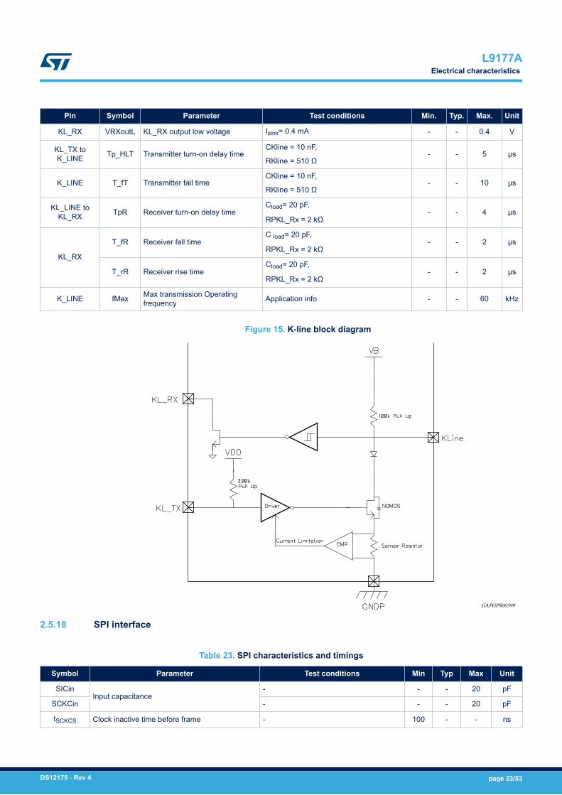
2.5.17 K-line
Table 22. K-Line interface electrical characteristics
Pin Symbol Parameter Test conditions Min. Typ. Max. Unit
KL_TX
ITXsource Transmitter input source current - 10 - 100 µA
ITXsink Transmitter input sink current KL_TX = VDD - - 2.1 µA
IKL_TX KL_TX Internal Pull-up - - 200 - kΩ
K_LINE
VKoutL Transmitter output low voltageIsinkK_LINE = 35 mA,
KL_TX = Low-1 - 1.5 V
VKinH Receiver input high voltage - 0.7xVB - VB V
VKinL Receiver input low voltage - -1 - 0.35xVB V
VKH Receiver input hysteresis - 0.05xVB - 0.3xVB V
IKleak Receiver leakage current KL_LINE = VB,KL_TX = High - - 1 µA
K_LINE
IKshort Transmitter short circuit current KL_LINE = VB, KL_TX = Low 60 - - mA
IKrev Reverse battery or GND losscurrent
ENABLE = KEY = VB = 0 V,
KL_LINE = -13.5- - 10 mA
IKpull-up KLINE internal pull-up KL_TX = High 60 - 140 kΩ
IKuv Under voltage current KEY = High, KL_TX = Low, VB = 13.5 V,KL_LINE = -1 V - - 1 mA
L9177AElectrical characteristics
DS12175 - Rev 4 page 22/53
Pin Symbol Parameter Test conditions Min. Typ. Max. Unit
KL_RX VRXoutL KL_RX output low voltage Isink= 0.4 mA - - 0.4 V
KL_TX toK_LINE Tp_HLT Transmitter turn-on delay time
CKline = 10 nF,
RKline = 510 Ω- - 5 µs
K_LINE T_fT Transmitter fall timeCKline = 10 nF,
RKline = 510 Ω- - 10 µs
KL_LINE toKL_RX TpR Receiver turn-on delay time
Cload= 20 pF,
RPKL_Rx = 2 kΩ- - 4 µs
KL_RX
T_fR Receiver fall timeC load= 20 pF,
RPKL_Rx = 2 kΩ- - 2 µs
T_rR Receiver rise timeCload= 20 pF,
RPKL_Rx = 2 kΩ- - 2 µs
K_LINE fMax Max transmission Operatingfrequency Application info - - 60 kHz
Figure 15. K-line block diagram
GAPGPS00599
2
2.5.18 SPI interface
Table 23. SPI characteristics and timings
Symbol Parameter Test conditions Min Typ Max Unit
SICinInput capacitance
- - - 20 pF
SCKCin - - - 20 pF
tSCKCS Clock inactive time before frame - 100 - - ns
L9177AElectrical characteristics
DS12175 - Rev 4 page 23/53

Symbol Parameter Test conditions Min Typ Max Unit
tCSSO Access time See (1) - - 500 ns
tSOdis Output data (SO) disable timeNo Capacitor on SO,
See (2)- - 500 ns
tlead Channels select (CS) lead time See (1) 500 - - ns
tSCKFSO Output valid time See (1), @ fCLK= 5.4 MHz 60 - - ns
tSOCS Output data (SO) disable time No capacitor on SO, see (1) - 500 ns
tSIsetup Input data (SI) set-up time @ fCLK= 5.4 MHz 20 - - ns
tSIhold Input data (SI) hold time @ fCLK= 5.4 MHz 20 - - ns
tSCK CLK period - 185 - - ns
tCSSCK Clock inactive time after frame - 600 - - ns
tCSN CS de asserted time - 600 - - ns
1. see Figure 17. SPI timing diagram2. see Figure 16. SO loading for disable time measurement
Figure 16. SO loading for disable time measurement
VDD
SO
1 kΩ
1 kΩ
+5 V
1.0 V
4.0 V
tSOdis SO
CS
GADG0412170958PS
Figure 17. SPI timing diagram
t CSSO
tSOCS
tCSSCK
t lead
t SCKCS
t SCKFSO
CS
SCK
DIN
DOUT
DIN23
DOUT23 DOUT22 DOUT21 DOUT20 DOUT... DOUT... DOUT... DOUT0
DIN22 DIN21 DIN20 DIN... DIN... DIN1 DIN0
GADG0412171035PS
L9177AElectrical characteristics
DS12175 - Rev 4 page 24/53

3 Functional description
3.1 Chip working conditions
Table 24. A outputs working conditions
- Standby Run mode VB_OV VB_UV Reset Over current Thermal warning
VDD_SB regulator ON ON ON ON ON Current limitation ON
VDD regulator OFF ON OFF OFF ON Current limitation OFF if linked with VDD currentlimitation
VDD_TRK regulator OFF ON OFF OFF ON Current limitation OFF if linked with VDD_TRK currentlimitation
All LS drivers OFF ON OFF OFF OFF Over current switch off ON
Diagnostics of all LS drivers OFF ON OFF OFF ON(1) - ON
HS Driver OFF ON OFF OFF OFF Current limitation ON
Stepper Motor Driver OFF ON OFF OFF OFF Over current switch off ON
K-line Transceiver OFF ON OFF OFF OFF Current limitation ON
VRS OFF ON OFF OFF OFF - ON
SPI Default Default Default Default Default ON ON
1. The diagnostic currents and comparator are switched on in reset condition.
3.2 Chip bias current generationThe Internal current generator circuit is buffering internal band-gap voltage (1.2 V typ.) on a high precisionexternal resistor (10 kΩ ±1 %) and generates an accurate current reference used to create all the chip biascurrents.
L9177AFunctional description
DS12175 - Rev 4 page 25/53

Figure 18. Current generator block diagram
GAPGPS00602
3.3 Power up/down sequencesThe figures below show the power-on, power-off and time diagram behaviour of the device.VDD_SB (standby voltage) rises together with battery input, and in standby it is always present if battery ispresent, no matter the KEY_IN status.When the KEY_IN signal rises up and remains stable for at least T_key_deglitch (see Table 7), the device goes inON state, meaning that all voltage regulators and functions are active.Wake-up is an intermediate status between standby and on mode, with current consumption higher than thestandby one.When Key_IN goes low, device goes in OFF mode but standby regulator remains ON.
L9177APower up/down sequences
DS12175 - Rev 4 page 26/53

Figure 19. Power-up sequence
GAPGPS00603
VB
VDD_SB
Key_IN V_Key_H
Vth_UV Tht
STBY Wake_UpT_key_deglitch
On State
Td_UV_rst
State
VDD
RESET
Figure 20. Power-down sequence
GAPGPS00604
VB
VDD_SB
Key_IN V_Key_L
VDD
RESET
Vth_UV
TfUV_reset
Reset signal detects a VDD undervoltage longer than TfUV_reset by going to low level. When VDD recovers tonormal level Reset signal returns to high level after Power_On_UV_Reset_Delay time (Td_UV_RST). The Resetsignal resets all the internal SPI registers to default value.
3.4 SPISPI is a standard four wires interface, that communicates with a data word of 24 bits. By means of SPI all thechannels can be driven in serial way and diagnosis is sent out.Timing of SPI's operations are reported inFigure 17. The input data (DIN) is read on the rising edge of the SPI's clock (SCLK), in the same way the outputdata (DOUT) must be read by the Microcontroller on the SCLK's rising edge.
3.4.1 Data in (DIN)DIN command is used to turn On/Off internal channels which do not have Parallel Input command, and to cleardiagnostic latches.DIN is decoded at the end of the frame if the integrity checks are passed.
L9177ASPI
DS12175 - Rev 4 page 27/53

Table 25. Data in (DIN) words content
DIN23 DIN22 DIN21 DIN20 DIN19 DIN18 DIN17 DIN16
Mask L_0 L_1 VRS Diag VRS Hys0 VRS Hys1 VRS Hys2 0
DIN15 DIN14 DIN13 DIN12 DIN11 DIN10 DIN9 DIN8
INJ1_0 INJ1_1 INJ2_0 INJ2_1 O2H_0 O2H_1 RLY1_0 RLY1_1
DIN7 DIN6 DIN5 DIN4 DIN3 DIN2 DIN1 DIN0
RLY2_0 RLY2_1 RLY3_0 RLY3_1 TACH_0 TACH_1 Clear diag Parity
Data in structure (MSB first)
• Mask bit is used to mask serial command for diagnosis only readings on DOUT:
0 - Read Diag. All DIN bits are ignored.1 - Write. All DIN are transferred into the internal registers.• Command bits are used to control the output drivers: (INJ1-2, O2H, RLY1-2-3, L and TACH) as described in
the following table:
Table 26. Data in command bits structure
xxx_0 xxx_1 Description
0 1 Turn-off driver / parallel polarity 0
1 1 Turn-on driver / parallel polarity 1
X 0 No change (the driver will maintain the previous condition)
• VRS Diag bit is used active high to enable diagnostic phase of VRS block, the diagnosis can be done onlywhen the phonic wheel is stopped.
• Programmable VRS Hysteresis: VRS hysteresis is programmable in 5 steps according to Table 27.• Clear Diag, when set to 1 generates a request to clear those diagnostic flags which are latched.• In addition odd parity bit (that is the last bit of the frame and includes in its calculation the "Don't care" bits)
is used for DIN word check together with falling clock edges count.
Table 27. Data in VRS hysteresis
Hys 0 Hys 1 Hys 2 Description
0 0 0 Auto adaptive hysteresis
1 0 0 Hys VRS = 100 mV
0 1 0 Hys VRS = 200 mV
1 1 0 Hys VRS = 350 mV
0 0 1 Hys VRS = 650 mV
1 0 1 Hys VRS = 1000 mV
1 1 1 Not Valid (Hys doesn't change)
3.4.2 Data out (DOUT)Status flags are sampled and sent out through DOUT pin at each R/W SPI operation. The structure of the 24 bitword is described in Table 28. A three bits diagnosis is provided for stepper motor driver, a two bit diagnosis for
L9177ASPI
DS12175 - Rev 4 page 28/53

other drivers. VRS diagnosis is coded as '0' means No Fault, while '1' means Fault. Over temperature warning iscoded as '0' means No Fault, while '1' means Fault.The SPI default value is: all bits set to zero.
Table 28. Data out (DOUT) words content
DOUT23 DOUT22 DOUT21 DOUT20 DOUT19 DOUT18 DOUT17 DOUT16
INJ1 Diag0 INJ1 Diag1 INJ2 Diag0 INJ2 Diag1 O2H Diag0 O2H Diag1 RLY1 Diag0 RLY1 Diag1
DOUT15 DOUT14 DOUT13 DOUT12 DOUT11 DOUT10 DOUT9 DOUT8
RLY2 Diag0 RLY2 Diag1 RLY3 Diag0 RLY3 Diag1 L Diag0 L Diag1 TACH Diag0 TACH Diag1
DOUT7 DOUT6 DOUT5 DOUT4 DOUT3 DOUT2 DOUT1 DOUT0
VRS Diag Thermal Warning Brdg1 Diag0 Brdg1 Diag1 Brdg1 Diag2 Brdg2 Diag0 Brdg2 Diag1 Brdg2 Diag2
Data out structure
Table 29. Two bits diagnosis (normal drivers)
Bit 0 Bit 1 Fault
0 0 No Fault
1 0 Short to Ground (OFF)
0 1 Open Load (OFF)
1 1 Overcurrent (ON)
Table 30. Three bits diagnosis (bridge stage)
Bit 0 Bit 1 Bit 2 Fault
0 0 0 No Fault
1 0 0 Short to Ground (OFF)
1 0 1 Short to VBAT (OFF)
0 1 0 Open Load (OFF)
1 1 0 Overcurrent (ON)
3.5 DiagnosisThe device provides a full set of diagnosis; deglitch timings listed below are digital, generated from internal clockand their accuracy is guaranteed by scan patterns and clock measurement.
3.5.1 Voltage regulators thermal warning and shutdownThe 5V linear voltage regulator/tracking regulator is shut down when the thermal shutdown temperature isreached and also the regulator is in current limitation. The shutdown is filtered with Tdcg filter of 30 µs ±25 %. Assoon as the over temperature disappears the regulator is switched on again. Over temperature flag without anylatch is present via SPI.
3.5.2 Overvoltage shut downIf the VB_off voltage is reached after Tdgc filtering time of 30 µs ±25 % the device enters a safety state where themain outputs are switched-off. Voltage regulators, all low side channels, stepper motor driver and KLINE areswitched off and reset is asserted. As soon as the battery goes below VB_off minus VB_off_h the device recoversstandard operation.
L9177ADiagnosis
DS12175 - Rev 4 page 29/53

3.5.3 Undervoltage shut downIf the VB_UV voltage is reached after analog Tdgc 1 µs ±20 % filtering time the device enters a safety state wheremain outputs are switched-off. Voltage regulators, all low side channels, stepper motor driver and KLINE areswitched off. As soon as the battery rises above VB_UV plus the hysteresis the device recovers normal operation.
Figure 21. An example of under and over voltage time diagram
VBVB
5V
5V
5V
VB
LIMITED VB
0
0
0
0
0
0
KEY
VDDVth_UV Tht
Td_UV_rst TfUV_reset
Tdgc_VB_OV
Td_UV_rst
VDD_TRK
HS_OUT
RST
BATTERY LINECONNECTION
STAND-BY IGNITION KEYSWITCH ON
IGNITION KEYSWITCH OFF
STAND-BY VDDUNDERVOLTAGE
VB OVERVOLTAGEPROTECTION
Td_UV_rst
Vth_UV Tht
VB_off VB_off
GADG0412171117PS
3.5.4 Low side on/off diagnosis (INJ, RLY's, TACH, O2H)About low side channels OFF diagnosis, the device issues a masking filter Tmask after channel turning off (fallingedge of driving command) to avoid false fault detecting due to output transition from low to high. Tmask is of 1 ms±25 % for all channels except for the relays, for which Tmask is 3.5 ms ±25 %. Once masking time has expired adeglitch filter Tdgc_noise of 3.6 µs ±40 % for noise immunity is activated. A fault longer than deglitch time islatched. OFF state diagnostic fault can be overwritten by ON state fault. OFF state fault does not prevent thedriver from switching on. The latched fault is cleared on request.During on-phase if an over current fault occurs the drivers enter in current limitation condition for a digital filteringtime Tdgc of 20 µs ±25 %,then it is switched OFF and the fault is latched. The channel is turned ON again byinput command transition. The latched fault is cleared on request via SPI.Over current fault has higher priority respect to OFF condition faults.
L9177ADiagnosis
DS12175 - Rev 4 page 30/53

Figure 22. Low side driver diagnosis time diagram
GAPGPS00606
L9177ADiagnosis
DS12175 - Rev 4 page 31/53

Figure 23. Low side driver diagnosis I-V relationship
GAPGPS00607
3.5.5 Current limited low side driver on/off diagnosisIn OFF condition diagnosis is the same as Low side, with Tmask 3.5 ms ±25 % and Tdgc_noise 3.6 µs ± 40 %,while in ON condition initial Inrush current is masked for Tmask_rush of 336 µs ±25 % then, if an over current faultoccurs the drivers enter in current limitation condition for a digital filtering time Tdgc of 20 µs ±25 %, then it isswitched OFF and the fault is latched. The channel is turned ON again by input command transition. The latchedfault is cleared on request via SPI. Over current fault has higher priority with respect to OFF condition faults.
L9177ADiagnosis
DS12175 - Rev 4 page 32/53

Figure 24. Current limited low side driver diagnosis time diagram
GAPGPS00608
3.5.6 Stepper motor driver OFF diagnosis (EN signal low and output in high impedance state)In OFF condition Short to GND/Short to VB or Open Load condition is continuously detected through a deglitchfilter of 125 µs ±25 %, after Tmask masking time of 1 ms ±25 % to filter ON/ OFF transition. To avoid falsediagnostic due to motor residual movement, the stepper has to be disabled at least 40 ms after the PWL signalhas been disabled. A fault longer than deglitch time is latched. OFF state diagnostic fault can be overwritten byON state fault. OFF state fault does not prevent the stepper from switching on. The latched fault is cleared onrequest.
3.5.7 Stepper motor driver ON diagnosis (EN signal high and output driven by input commands)In ON condition when over current fault is detected and validated after digital filtering time Tdgc of 20 µs ±25 %,the bridge is turned OFF and the fault is latched. The bridge is turned ON again by input command EN transition.The latched fault is cleared on request. Over current fault has higher priority with respect to OFF condition faults.Each Bridge has dedicated fault diagnosis detection coded by three bits.
L9177ADiagnosis
DS12175 - Rev 4 page 33/53

Figure 25. Stepper motor driver diagnosis time diagram
GAPGPS00609
Figure 26. Stepper motor driver diagnosis I-V relationship
GAPGPS00610
L9177ADiagnosis
DS12175 - Rev 4 page 34/53

3.5.8 VRS diagnosisVRS block enters diagnosis phase on request via SPI and then generates a Fault bit. If the fault exceeds the Tdgcfilter time of 30 µs ±20 %, it is latched. The latched fault is cleared on request via SPI. The VRS diagnostic canonly be activated when the phonic wheel is in stop condition.
Figure 27. VRS diagnosis I-V relationship
GAPGPS00611
3.6 VRS interface
3.6.1 Function characteristicThe flying wheel interface is an interface between the µP and the flying wheel sensor: it conditions signal comingfrom magnetic pick-up sensor or hall effect sensor and feeds the digital signal to microcontroller that extractsflying wheel rotational position, angular speed and acceleration.
Figure 28. VRS typical characteristics
GAPGPS00571
Vdiff
ω IN +VRS
IN -
Rs
Ls
L9177AVRS interface
DS12175 - Rev 4 page 35/53

Figure 29. VRS interface structure
GAPGPS00612
VRS voltage Int_vrsAuto adaptativeHysteresis
Auto adaptativeTime filtering block Out_vrs
3.6.2 Auto-adaptative hysteresisInput signals difference is obtained through a full differential amplifier; its output, DV signal, is fed to peakdetection circuit and then to A/D converter implemented with 4 voltage comparator (5 levels Pvi).Output of A/D issent to Logic block (hysteresis selection Table 32) that implements correlation function between Peak voltage andhysteresis value; hysteresis value is used by square filtering circuit which conditions DV signal.
Figure 30. Auto-adaptive hysteresis block diagram
GAPGPS00613
H
H
PVi
DV
VRS voltage
Hysteresis Squarer Circuit andTemporal Filtering
HysteresisValue
HysteresisSelection
Table
Peak DetectionCircuit
AD converter
PV
+
–
Int_vrs
Figure 31. Hysteresis output voltage level
GAPGPS00614
H4
H3
H2
H1
H0
Hysteresis outputvoltage (mV)
0 Quantized peak detectoroutput voltage (mV)
PV1 PV2 PV3 PV4
To the previous 5 levels PV = [0 PV1 PV2 PV3 PV4] correspond to a set of 5 thresholds:• H = [HO HIH2 H3 H4]
The advised values for the previous defined vectors are:• PV = [0 PV1 PV2 PV3 PV4] = [0, 900, 1560, 2230, 2900] mV• H = [H0 H1 H2 H3 H4] = [100, 200, 350, 650, 1000] mV
L9177AVRS interface
DS12175 - Rev 4 page 36/53

Table 31. Peak voltage detector precision
Pick voltage [PV]Value
UnitMin. Typ. Max.
PV1 850 900 950 mV
PV2 1452 1560 1638 mV
PV3 2118 2230 2341 mV
PV4 2755 2900 3045 mV
Table 32. Hysteresis threshold precision
Pick voltage [PV]Value
UnitMin. Typ. Max.
H0 70 100 130 mV
HV1 140 200 220 mV
HV2 250 347 390 mV
HV3 490 644 720 mV
HV4 730 1000 1120 mV
Note: Hysteresis voltages are achieved by injecting an hysteresis bias current on V RIN± external resistors (typ. 10 kΩeach, see Figure 38). The resulting HV voltage is HV = I_hys * Rtyp. Changing the value of R the hysteresisvalue would change in a linear mode.
L9177AVRS interface
DS12175 - Rev 4 page 37/53

Figure 32. Input-output behaviour of VRS interface
0.1
0.15
VRS voltage [V]
threshold
Squared signal
hysteresis
0.05
0.0
-0.05
-0.1
0.8
1
0.6
0.4
0.2
0
0.53 0.535DT1 DT2
DT2<TfTf
Tf = Filtering timeDT2>Tf
0.54 0.545 0.55 0.555 0.56
0.53 0.535 0.54 0.545 0.55 0.555 0.56GAPGPS00615
3.6.3 Auto-adaptative time filterThis characteristic is useful to set the best internal filter time as function of the input signalfrequency.The Tfilter time depends on the previous period duration Tn according to the following formula:Tfilter(n+1) = 1/32 * Tn if Tn > Tfilter(n)The filtering time purpose is to filter very short spikes.The digital filtering time is applied to internal squared signal (int_vrs), obtained by voltage comparators.The output of time filtering block is out_vrs signal.The filtering time Tfilter is applied to int_vrs signal in two different ways:• Rising edge: if int_vrs high level lasts less than Tfilter, out_vrs is not set to high level.• In absence of any spikes during input signal rising edge out_vrs signal is expected with a delay of Tfilter
time.• Falling edge: the falling edge of int_vrs is not delayed through time filtering block: after falling edge for a time
Tfilter any other transition on int_vrs signal is ignored
The initial value (Default) and maximum for Tfilter must be considered at RPM_min = 20 e.g. Tmax filter = 180 µs.The minimum available value is Tmin filter = 2.8 µs.
L9177AVRS interface
DS12175 - Rev 4 page 38/53

Figure 33. Auto-adaptative time filter behaviour 1
GAPGPS00616
8000
1/32 * T(n+3)1/32 * T(n+2)
1/32 * T(n+1)1/32 * T(n)
T(n) T(n+1) T(n+2) T(n+3)
1/32 * T(n-1)
Vdiff
Vout
RPM
RPM max
RPM min
Vdiff max
Vdiff min
[s]
[s]
[s]
Hys
Figure 34. Auto-adaptative time filter behaviour 2
GAPGPS00617
8000
1/32 * T(n+3)1/32 * T(n+2)
1/32 * T(n+1)1/32 * T(n)
1/32 * T(n)
T(n) T(n+1) T(n+2) T(n+3)
1/32 * T(n-1)
Vdiff
Vout
FilterTime
MaskTime
Vdiff max
Vdiff min
[s]
[s]
Hys
L9177AVRS interface
DS12175 - Rev 4 page 39/53

4 Low side drivers
Low side drivers have a voltage slew rate control during switch-on/off phase to reduce emissions.The slew-rate control is achieved controlling the gate charging current and the behavior is described in Figure 35and Figure 36.
Figure 35. Low side drivers slew rate implementation
GAPGPS00618
VLVT
VB
VDD
IP1
IP2
CMD
IN1
IN2
VREF
+
+
L9177ALow side drivers
DS12175 - Rev 4 page 40/53

Figure 36. Low side drivers slew rate
GAPGPS00619
IP2
IP1
IN1
IN2
IN1
IP1Igate
Vgate
Igate
Vgate
VOUTVOUT
IOUT
VLVTVLVT
80%20%
not controlledIOUT not controlled
At switch-on command the charging current is provided by current generator IP1 and is kept constant until theoutput voltage is decreased of roughly 80% of typical battery level. At this point the low side transistor is on andVLVT signal is set to logic 1 to connect IP2 current generator in parallel with IP1, completing the gate chargecurve and providing maximum gate drive.When the power transistor is switched-off the gate is discharged quickly using both IN1 and IN2 currents; as soonas the output voltage reaches roughly 20 % of the nominal battery voltage only IN1 is kept connected to completethe gate discharging.In Table 33 the values for IPx and INx current generators are reported for each low side.As an example Figure 37 shows the resulting slew rate, in typical conditions, of O2H low side driver.
Table 33. Values for IPx and INx current generators for each low side
Low side IP1 IP2 IN1 IN2 Unit
O2H 243 81 253 337 µA
INJ 174 23 180 124 µA
RLY’s 78 0 80 120 µA
L 78 0 62 119 µA
TACH 22 0 21 25 µA
L9177ALow side drivers
DS12175 - Rev 4 page 41/53

Figure 37. O2H low side driver slew rate
GAPGPS00620
TYP condition (Rload = 10ohm, Cload = 10nF) @ room temperatureVout
Iout
13V
4.41V/µs 4.41V/µs
1.27A
432mA/µs 450mA/µs
20%
2V2.65V
2V1.8V
60ns 100ns
20%
80% 80%
[s]
[s]
L9177ALow side drivers
DS12175 - Rev 4 page 42/53

5 Application circuit
Figure 38. Application circuit
R_ext
R_VRS-
R_VRS+RF_1
CF_2CF_1
C_OUTD
C_OUTC
C_OUTB
C_OUTA
C_VRS+_in
C_VRS-_in
RF_2
C_VRS-_out
C_VRS+_out
RX_pull-up
VDD
ToR
elay
s
C1VB_MAIN
R_KEY
SPC5x L9177A
IN2
VDD_StandBy
KEY
IN_REL2
IN_REL1
R_VROUT
R_reset
VDD
VDD
INO2H
KL_LINE
SCK
/CS
SO
SI
ILS_TACH
EN
PWM
DIR
VROUT
IN1
ENABLE
RESET
GNDO2H GND_A/P GND_P2 GND_P1
VB
Battery BatteryTo Sensor
VB1 VDD_TRK HS_OUT
INJ2Injector 2
VB
Injector 1
GNDJ
VB
INJ1
VRIN+
OUTD
OUTC
OUTB
OUTA
O2H
TACH
VRIN-
REXT
KL_RX
KL_TX
L
REL3
REL2
REL1
SensorTo Oxygen
To Tachimeter
Pick-UpFrom
Motor
Stepper
GAPG1303150713PS
D1 C_Vtrk
C_VDD_stby
C_VDD
5.1 Bill of material
Table 34. Bill of material
Block Component Name Usage Min Typ Max Unit
Supply Capacitor C1VB_MAIN Bulk capacitor 220 µF
Diode D1 Reverse polarization protection diode
Key Resistor R_Key Current limiting resistor 20 kΩ
L9177AApplication circuit
DS12175 - Rev 4 page 43/53

Block Component Name Usage Min Typ Max Unit
Rext Resistor R_ext Pull-up resistor 10 (1%) kΩ
Reset Resistor R_reset Pull-up resistor 1 kΩ
VDD CapacitorC_VDD value
Output capacitor (Ceramic or Tantalum)4.7 60 µF
C_VDD ESR 1.5 Ω
VDD_trk CapacitorC_Vtrk value
Output capacitor2.2 100 µF
C_Vtrk ESR 10 100 mΩ
Vdd_sby CapacitorC_VDD_stby value
Output capacitor1 10 µF
C_VDD_stby ESR 200 mΩ
VRS Capacitor C_VRS+_in Filter Capacitor 100 pF
VRS Capacitor C_VRS-_in Filter Capacitor 100 pF
VRS Capacitor C_VRS+_out Filter Capacitor 470 pF
VRS Capacitor C_VRS-_out Filter Capacitor 470 pF
VRS Resistor R_VRS+ Current limiting resistor 10 kΩ
VRS Resistor R_VRS- Current limiting resistor 10 kΩ
VRS Capacitor CF_1 Filter Capacitor 470 pF
VRS Capacitor CF_2 Filter Capacitor 100 nF
VRS Resistor RF_1 Filter resistor 33 kΩ
VRS Resistor RF_2 Filter resistor 33 kΩ
VRS Resistor R_VROUT Pull-up resistor 10 kΩ
K-Line Resistor RX_pull-up Pull-up resistor 2 kΩ
Stepper Capacitor C_OUTA EMI filter capacitor 10 nF
Stepper Capacitor C_OUTB EMI filter capacitor 10 nF
Stepper Capacitor C_OUTC EMI filter capacitor 10 nF
Stepper Capacitor C_OUTD EMI filter capacitor 10 nF
L9177ABill of material
DS12175 - Rev 4 page 44/53

6 Package information
In order to meet environmental requirements, ST offers these devices in different grades of ECOPACK®
packages, depending on their level of environmental compliance. ECOPACK® specifications, grade definitionsand product status are available at: www.st.com. ECOPACK® is an ST trademark.
6.1 TQFP64 (10x10x1 mm exp. pad down) package information
Figure 39. TQFP64 (10x10x1 mm exp. pad down) package outline
SECTION B-B
S 0.25
L
b1
c c1
(b)
(L1)
R1
R2
GAUGE PLANE
θ
7278840_Rev9.0_PkgCode_9I
D
N
(N-4) x
123
D1
EE1
D
A
A A
(see SECTION A-A)
A
A2 A1
C H
ccc C
e
b
D2D3
E3 E2D1/4
E1/4
B
4x N/4 TIPS
4x
D1/4
E1/4
─ 0.05
aaa C A-B DbbbH A-B D
AM D
GAPGPS03451
BOTTOM VIEW
SECTION A-A
WITH PLATING
θ2 θ1
θ3
BASE METAL
ddd
TOP VIEW
L9177APackage information
DS12175 - Rev 4 page 45/53
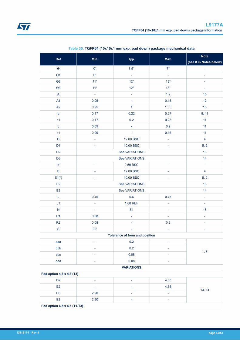
Table 35. TQFP64 (10x10x1 mm exp. pad down) package mechanical data
Ref Min. Typ. Max.Note
(see # in Notes below)
Ө 0° 3.5° 7° -
Ө1 0° - - -
Ө2 11° 12° 13° -
Ө3 11° 12° 13° -
A - - 1.2 15
A1 0.05 - 0.15 12
A2 0.95 1 1.05 15
b 0.17 0.22 0.27 9, 11
b1 0.17 0.2 0.23 11
c 0.09 - 0.2 11
c1 0.09 - 0.16 11
D - 12.00 BSC - 4
D1 - 10.00 BSC - 5, 2
D2 See VARIATIONS 13
D3 See VARIATIONS 14
e - 0.50 BSC - -
E - 12.00 BSC - 4
E1(*) - 10.00 BSC - 5, 2
E2 See VARIATIONS 13
E3 See VARIATIONS 14
L 0.45 0.6 0.75 -
L1 - 1.00 REF - -
N - 64 - 16
R1 0.08 - - -
R2 0.08 - 0.2 -
S 0.2 - - -
Tolerance of form and position
aaa - 0.2 -
1, 7bbb - 0.2 -
ccc - 0.08 -
ddd - 0.08 -
VARIATIONS
Pad option 4.3 x 4.3 (T3)
D2 - - 4.65
13, 14E2 - - 4.65
D3 2.90 - -
E3 2.90 - -
Pad option 4.5 x 4.5 (T1-T3)
L9177ATQFP64 (10x10x1 mm exp. pad down) package information
DS12175 - Rev 4 page 46/53

Ref Min. Typ. Max.Note
(see # in Notes below)
D2 - - 4.98
13, 14E2 - - 4.98
D3 3.29 - -
E3 3.29 - -
Pad option 6.0 x 6.0 (T3)
D2 - - 6.40
13, 14E2 - - 6.40
D3 4.80 - -
E3 4.80 - -
Pad option 7.5 x 7.5 (T1)
D2 - - 7.60
13, 14E2 - - 7.60
D3 7.30 - -
E3 7.30 - -
Notes
1. Dimensioning and tolerancing schemes conform to ASME Y14.5M-1994.2. The Top package body size may be smaller than the bottom package size up to 0.15 mm.3. Datum A-B and D to be determined at datum plane H.4. To be determined at seating datum plane C.5. Dimensions D1 and E1 do not include mold flash or protrusions. Allowable mold flash or protrusions is “0.25
mm” per side. D1 and E1 are Maximum plastic body size dimensions including mold mismatch.6. Details of pin 1 identifier are optional but must be located within the zone indicated.7. All Dimensions are in millimeters.8. No intrusion allowed inwards the leads.9. Dimension “b” does not include dambar protrusion. Allowable dambar protrusion shall not cause the lead
width to exceed the maximum “b” dimension by more than 0.08 mm. Dambar cannot be located on the lowerradius or the foot. Minimum space between protrusion and an adjacent lead is 0.07 mm for 0.4 mm and 0.5mm pitch packages.
10. Exact shape of each corner is optional.11. These dimensions apply to the flat section of the lead between 0.10 mm and 0.25 mm from the lead tip.12. A1 is defined as the distance from the seating plane to the lowest point on the package body.13. Dimensions D2 and E2 show the maximum exposed metal area on the package surface where the exposed
pad is located (if present). It includes all metal protrusions from exposed pad itself.14. Dimensions D3 and E3 show the minimum solderable area, defined as the portion of exposed pad which is
guaranteed to be free from resin flashes/bleeds, bordered by internal edge of inner groove.15. The optional exposed pad is generally coincident with the top or bottom side of the package and not allowed
to protrude beyond that surface.16. “N” is the number of terminal positions for the specified body size.
L9177ATQFP64 (10x10x1 mm exp. pad down) package information
DS12175 - Rev 4 page 47/53

Revision history
Table 36. Document revision history
Date Revision Changes
20-Sep-2017 1 Initial release.
29-Sep-2017 2
Updated Table 1. Pin function pin 27 column "Class" from SIGNAL to PWR;
Updated Section 2.1.1 Supply voltage;Changed titles: Section 3.5.6 Stepper motor driver OFF diagnosis (EN signal low andoutput in high impedance state) and Section 3.5.7 Stepper motor driver ON diagnosis(EN signal high and output driven by input commands);
Updated "Notes" in the Table 4. ESD protection;
Updated unit of "T_key_deglitch" parameter" in Table 7. Key electrical characteristicsand "R_pull" in Table 8. Digital pins characteristics.
05-Dec-2017 3
Corrected typos in the titles of the sections: Section 3.5.6 Stepper motor driver OFFdiagnosis (EN signal low and output in high impedance state) andSection 3.5.7 Stepper motor driver ON diagnosis (EN signal high and output driven byinput commands).
Updated Table 1. Pin function.
Substituted in the datasheet (texts, tables and drawings) "Vdd" with "VDD".
Updated: Figure 5. 5 V main regulator block diagram; Section 2.5.9 High side switch;Figure 10. Low-side driver block diagram; Figure 16. SO loading for disable timemeasurement; Figure 17. SPI timing diagram; Section 3.4.1 Data in (DIN);Section 3.4.2 Data out (DOUT); Section 3.5.3 Undervoltage shut down;Section 5.1 Bill of material.
26-Nov-2018 4
Updated:
Section Description; Section 2.1 Operating range; Section 2.2 Absolute maximumratings; Table 8. Digital pins characteristics; Figure 5. 5 V main regulator blockdiagram; Figure 3. Input threshold; Table 17. Current limited LSD drivercharacteristics; Section 3.5.5 Current limited low side driver on/off diagnosis;Figure 17. SPI timing diagram; Figure 19. Power-up sequence; Figure 20. Power-down sequence; Section 3.4.1 Data in (DIN); Figure 21. An example of under and overvoltage time diagram; Section 3.5.8 VRS diagnosis; Figure 38. Application circuit;Table 34. Bill of material.Changed in all document "LAMP" pin in "L" (Current limited LSD). UpdatedSection 2.5 Electrical characteristics.
L9177A
DS12175 - Rev 4 page 48/53

Contents
1 Block diagram and pin description . . . . . . . . . . . . . . . . . . . . . . . . . . . . . . . . . . . . . . . . . . . . . . . . .3
1.1 Block diagram . . . . . . . . . . . . . . . . . . . . . . . . . . . . . . . . . . . . . . . . . . . . . . . . . . . . . . . . . . . . . . . . . 3
1.2 Pin description . . . . . . . . . . . . . . . . . . . . . . . . . . . . . . . . . . . . . . . . . . . . . . . . . . . . . . . . . . . . . . . . . 4
2 Electrical specifications . . . . . . . . . . . . . . . . . . . . . . . . . . . . . . . . . . . . . . . . . . . . . . . . . . . . . . . . . . .7
2.1 Operating range . . . . . . . . . . . . . . . . . . . . . . . . . . . . . . . . . . . . . . . . . . . . . . . . . . . . . . . . . . . . . . . 7
2.1.1 Supply voltage . . . . . . . . . . . . . . . . . . . . . . . . . . . . . . . . . . . . . . . . . . . . . . . . . . . . . . . . . . 7
2.2 Absolute maximum ratings. . . . . . . . . . . . . . . . . . . . . . . . . . . . . . . . . . . . . . . . . . . . . . . . . . . . . . . 7
2.3 Latch-up test . . . . . . . . . . . . . . . . . . . . . . . . . . . . . . . . . . . . . . . . . . . . . . . . . . . . . . . . . . . . . . . . . . 9
2.4 Temperature ranges and thermal data . . . . . . . . . . . . . . . . . . . . . . . . . . . . . . . . . . . . . . . . . . . . . 9
2.5 Electrical characteristics. . . . . . . . . . . . . . . . . . . . . . . . . . . . . . . . . . . . . . . . . . . . . . . . . . . . . . . . . 9
2.5.1 Supply. . . . . . . . . . . . . . . . . . . . . . . . . . . . . . . . . . . . . . . . . . . . . . . . . . . . . . . . . . . . . . . . . 9
2.5.2 Key . . . . . . . . . . . . . . . . . . . . . . . . . . . . . . . . . . . . . . . . . . . . . . . . . . . . . . . . . . . . . . . . . . . 9
2.5.3 Digital pins . . . . . . . . . . . . . . . . . . . . . . . . . . . . . . . . . . . . . . . . . . . . . . . . . . . . . . . . . . . . 10
2.5.4 Digital output pins . . . . . . . . . . . . . . . . . . . . . . . . . . . . . . . . . . . . . . . . . . . . . . . . . . . . . . . 10
2.5.5 5 V voltage regulator . . . . . . . . . . . . . . . . . . . . . . . . . . . . . . . . . . . . . . . . . . . . . . . . . . . . . 11
2.5.6 Reset . . . . . . . . . . . . . . . . . . . . . . . . . . . . . . . . . . . . . . . . . . . . . . . . . . . . . . . . . . . . . . . . 12
2.5.7 5 V tracking voltage regulator . . . . . . . . . . . . . . . . . . . . . . . . . . . . . . . . . . . . . . . . . . . . . . 12
2.5.8 Standby regulator . . . . . . . . . . . . . . . . . . . . . . . . . . . . . . . . . . . . . . . . . . . . . . . . . . . . . . . 13
2.5.9 High side switch . . . . . . . . . . . . . . . . . . . . . . . . . . . . . . . . . . . . . . . . . . . . . . . . . . . . . . . . 14
2.5.10 Injector driver . . . . . . . . . . . . . . . . . . . . . . . . . . . . . . . . . . . . . . . . . . . . . . . . . . . . . . . . . . 15
2.5.11 Relay drivers . . . . . . . . . . . . . . . . . . . . . . . . . . . . . . . . . . . . . . . . . . . . . . . . . . . . . . . . . . . 16
2.5.12 Current limited low side driver (LSD). . . . . . . . . . . . . . . . . . . . . . . . . . . . . . . . . . . . . . . . . 17
2.5.13 Tachometer driver . . . . . . . . . . . . . . . . . . . . . . . . . . . . . . . . . . . . . . . . . . . . . . . . . . . . . . . 18
2.5.14 Stepper motor driver . . . . . . . . . . . . . . . . . . . . . . . . . . . . . . . . . . . . . . . . . . . . . . . . . . . . . 18
2.5.15 O2 sensor heater driver . . . . . . . . . . . . . . . . . . . . . . . . . . . . . . . . . . . . . . . . . . . . . . . . . . 20
2.5.16 Variable reluctance sensor interface . . . . . . . . . . . . . . . . . . . . . . . . . . . . . . . . . . . . . . . . . 21
2.5.17 K-line . . . . . . . . . . . . . . . . . . . . . . . . . . . . . . . . . . . . . . . . . . . . . . . . . . . . . . . . . . . . . . . . 22
2.5.18 SPI interface . . . . . . . . . . . . . . . . . . . . . . . . . . . . . . . . . . . . . . . . . . . . . . . . . . . . . . . . . . . 23
3 Functional description . . . . . . . . . . . . . . . . . . . . . . . . . . . . . . . . . . . . . . . . . . . . . . . . . . . . . . . . . . . .25
3.1 Chip working conditions . . . . . . . . . . . . . . . . . . . . . . . . . . . . . . . . . . . . . . . . . . . . . . . . . . . . . . . . 25
L9177AContents
DS12175 - Rev 4 page 49/53

3.2 Chip bias current generation . . . . . . . . . . . . . . . . . . . . . . . . . . . . . . . . . . . . . . . . . . . . . . . . . . . . 25
3.3 Power up/down sequences . . . . . . . . . . . . . . . . . . . . . . . . . . . . . . . . . . . . . . . . . . . . . . . . . . . . . 26
3.4 SPI . . . . . . . . . . . . . . . . . . . . . . . . . . . . . . . . . . . . . . . . . . . . . . . . . . . . . . . . . . . . . . . . . . . . . . . . . 27
3.4.1 Data in (DIN) . . . . . . . . . . . . . . . . . . . . . . . . . . . . . . . . . . . . . . . . . . . . . . . . . . . . . . . . . . . 27
3.4.2 Data out . . . . . . . . . . . . . . . . . . . . . . . . . . . . . . . . . . . . . . . . . . . . . . . . . . . . . . . . . . . . . . 28
3.5 Diagnosis . . . . . . . . . . . . . . . . . . . . . . . . . . . . . . . . . . . . . . . . . . . . . . . . . . . . . . . . . . . . . . . . . . . . 29
3.5.1 Voltage regulators thermal warning and shutdown . . . . . . . . . . . . . . . . . . . . . . . . . . . . . . 29
3.5.2 Overvoltage shut down . . . . . . . . . . . . . . . . . . . . . . . . . . . . . . . . . . . . . . . . . . . . . . . . . . . 29
3.5.3 Undervoltage shut down . . . . . . . . . . . . . . . . . . . . . . . . . . . . . . . . . . . . . . . . . . . . . . . . . . 30
3.5.4 Low side on/off diagnosis (INJ, RLY's, TACH, O2H) . . . . . . . . . . . . . . . . . . . . . . . . . . . . . 30
3.5.5 Current limited low side driver on/off diagnosis . . . . . . . . . . . . . . . . . . . . . . . . . . . . . . . . . 32
3.5.6 Stepper motor driver OFF diagnosis (EN signal low and output in high impedance state). 33
3.5.7 Stepper motor driver ON diagnosis (EN signal high and output driven by input commands) .. . . . . . . . . . . . . . . . . . . . . . . . . . . . . . . . . . . . . . . . . . . . . . . . . . . . . . . . . . . . . . . . . . . . . 33
3.5.8 VRS diagnosis . . . . . . . . . . . . . . . . . . . . . . . . . . . . . . . . . . . . . . . . . . . . . . . . . . . . . . . . . 34
3.6 VRS interface. . . . . . . . . . . . . . . . . . . . . . . . . . . . . . . . . . . . . . . . . . . . . . . . . . . . . . . . . . . . . . . . . 35
3.6.1 Function characteristic . . . . . . . . . . . . . . . . . . . . . . . . . . . . . . . . . . . . . . . . . . . . . . . . . . . 35
3.6.2 Auto-adaptative hysteresis . . . . . . . . . . . . . . . . . . . . . . . . . . . . . . . . . . . . . . . . . . . . . . . . 36
3.6.3 Auto-adaptative time filter . . . . . . . . . . . . . . . . . . . . . . . . . . . . . . . . . . . . . . . . . . . . . . . . . 38
4 Low side drivers . . . . . . . . . . . . . . . . . . . . . . . . . . . . . . . . . . . . . . . . . . . . . . . . . . . . . . . . . . . . . . . . . .40
5 Application circuit . . . . . . . . . . . . . . . . . . . . . . . . . . . . . . . . . . . . . . . . . . . . . . . . . . . . . . . . . . . . . . . .43
5.1 Bill of material . . . . . . . . . . . . . . . . . . . . . . . . . . . . . . . . . . . . . . . . . . . . . . . . . . . . . . . . . . . . . . . . 43
6 Package information. . . . . . . . . . . . . . . . . . . . . . . . . . . . . . . . . . . . . . . . . . . . . . . . . . . . . . . . . . . . . .45
6.1 TQFP64 (10x10x1 mm exp. pad down) package information . . . . . . . . . . . . . . . . . . . . . . . . . 45
Revision history . . . . . . . . . . . . . . . . . . . . . . . . . . . . . . . . . . . . . . . . . . . . . . . . . . . . . . . . . . . . . . . . . . . . . . .48
L9177AContents
DS12175 - Rev 4 page 50/53

List of tablesTable 1. Pin function . . . . . . . . . . . . . . . . . . . . . . . . . . . . . . . . . . . . . . . . . . . . . . . . . . . . . . . . . . . . . . . . . . . . . . . . 4Table 2. Operating conditions . . . . . . . . . . . . . . . . . . . . . . . . . . . . . . . . . . . . . . . . . . . . . . . . . . . . . . . . . . . . . . . . . 7Table 3. Absolute maximum ratings . . . . . . . . . . . . . . . . . . . . . . . . . . . . . . . . . . . . . . . . . . . . . . . . . . . . . . . . . . . . . 7Table 4. ESD protection . . . . . . . . . . . . . . . . . . . . . . . . . . . . . . . . . . . . . . . . . . . . . . . . . . . . . . . . . . . . . . . . . . . . . 8Table 5. Temperature ranges and thermal data . . . . . . . . . . . . . . . . . . . . . . . . . . . . . . . . . . . . . . . . . . . . . . . . . . . . . 9Table 6. Supply electrical characteristics . . . . . . . . . . . . . . . . . . . . . . . . . . . . . . . . . . . . . . . . . . . . . . . . . . . . . . . . . . 9Table 7. Key electrical characteristics . . . . . . . . . . . . . . . . . . . . . . . . . . . . . . . . . . . . . . . . . . . . . . . . . . . . . . . . . . . 10Table 8. Digital pins characteristics. . . . . . . . . . . . . . . . . . . . . . . . . . . . . . . . . . . . . . . . . . . . . . . . . . . . . . . . . . . . . 10Table 9. Digital output pins characteristics . . . . . . . . . . . . . . . . . . . . . . . . . . . . . . . . . . . . . . . . . . . . . . . . . . . . . . . . 11Table 10. VDD output electrical characteristics. . . . . . . . . . . . . . . . . . . . . . . . . . . . . . . . . . . . . . . . . . . . . . . . . . . . . . 11Table 11. Reset function electrical characteristics. . . . . . . . . . . . . . . . . . . . . . . . . . . . . . . . . . . . . . . . . . . . . . . . . . . . 12Table 12. VDD_TRK output electrical characteristics . . . . . . . . . . . . . . . . . . . . . . . . . . . . . . . . . . . . . . . . . . . . . . . . . 13Table 13. VDD_SB output electrical characteristics. . . . . . . . . . . . . . . . . . . . . . . . . . . . . . . . . . . . . . . . . . . . . . . . . . . 13Table 14. HS_OUT output electrical characteristics . . . . . . . . . . . . . . . . . . . . . . . . . . . . . . . . . . . . . . . . . . . . . . . . . . 14Table 15. Injector driver electrical characteristic . . . . . . . . . . . . . . . . . . . . . . . . . . . . . . . . . . . . . . . . . . . . . . . . . . . . . 15Table 16. Relay driver characteristics . . . . . . . . . . . . . . . . . . . . . . . . . . . . . . . . . . . . . . . . . . . . . . . . . . . . . . . . . . . . 17Table 17. Current limited LSD driver characteristics . . . . . . . . . . . . . . . . . . . . . . . . . . . . . . . . . . . . . . . . . . . . . . . . . . 17Table 18. Tachometer driver electrical characteristics . . . . . . . . . . . . . . . . . . . . . . . . . . . . . . . . . . . . . . . . . . . . . . . . . 18Table 19. Stepper motor driver electrical characteristics . . . . . . . . . . . . . . . . . . . . . . . . . . . . . . . . . . . . . . . . . . . . . . . 18Table 20. O2 sensor heater driver characteristics . . . . . . . . . . . . . . . . . . . . . . . . . . . . . . . . . . . . . . . . . . . . . . . . . . . . 20Table 21. Variable reluctance sensor interface electrical characteristics. . . . . . . . . . . . . . . . . . . . . . . . . . . . . . . . . . . . . 21Table 22. K-Line interface electrical characteristics. . . . . . . . . . . . . . . . . . . . . . . . . . . . . . . . . . . . . . . . . . . . . . . . . . . 22Table 23. SPI characteristics and timings . . . . . . . . . . . . . . . . . . . . . . . . . . . . . . . . . . . . . . . . . . . . . . . . . . . . . . . . . 23Table 24. A outputs working conditions . . . . . . . . . . . . . . . . . . . . . . . . . . . . . . . . . . . . . . . . . . . . . . . . . . . . . . . . . . . 25Table 25. Data in (DIN) words content . . . . . . . . . . . . . . . . . . . . . . . . . . . . . . . . . . . . . . . . . . . . . . . . . . . . . . . . . . . 28Table 26. Data in command bits structure . . . . . . . . . . . . . . . . . . . . . . . . . . . . . . . . . . . . . . . . . . . . . . . . . . . . . . . . . 28Table 27. Data in VRS hysteresis . . . . . . . . . . . . . . . . . . . . . . . . . . . . . . . . . . . . . . . . . . . . . . . . . . . . . . . . . . . . . . . 28Table 28. Data out (DOUT) words content . . . . . . . . . . . . . . . . . . . . . . . . . . . . . . . . . . . . . . . . . . . . . . . . . . . . . . . . . 29Table 29. Two bits diagnosis (normal drivers) . . . . . . . . . . . . . . . . . . . . . . . . . . . . . . . . . . . . . . . . . . . . . . . . . . . . . . 29Table 30. Three bits diagnosis (bridge stage). . . . . . . . . . . . . . . . . . . . . . . . . . . . . . . . . . . . . . . . . . . . . . . . . . . . . . . 29Table 31. Peak voltage detector precision . . . . . . . . . . . . . . . . . . . . . . . . . . . . . . . . . . . . . . . . . . . . . . . . . . . . . . . . . 37Table 32. Hysteresis threshold precision . . . . . . . . . . . . . . . . . . . . . . . . . . . . . . . . . . . . . . . . . . . . . . . . . . . . . . . . . . 37Table 33. Values for IPx and INx current generators for each low side. . . . . . . . . . . . . . . . . . . . . . . . . . . . . . . . . . . . . . 41Table 34. Bill of material . . . . . . . . . . . . . . . . . . . . . . . . . . . . . . . . . . . . . . . . . . . . . . . . . . . . . . . . . . . . . . . . . . . . . 43Table 35. TQFP64 (10x10x1 mm exp. pad down) package mechanical data . . . . . . . . . . . . . . . . . . . . . . . . . . . . . . . . . 46Table 36. Document revision history . . . . . . . . . . . . . . . . . . . . . . . . . . . . . . . . . . . . . . . . . . . . . . . . . . . . . . . . . . . . . 48
L9177AList of tables
DS12175 - Rev 4 page 51/53

List of figuresFigure 1. Block diagram . . . . . . . . . . . . . . . . . . . . . . . . . . . . . . . . . . . . . . . . . . . . . . . . . . . . . . . . . . . . . . . . . . . . 3Figure 2. Pin connection (top view) . . . . . . . . . . . . . . . . . . . . . . . . . . . . . . . . . . . . . . . . . . . . . . . . . . . . . . . . . . . . . 4Figure 3. Input threshold . . . . . . . . . . . . . . . . . . . . . . . . . . . . . . . . . . . . . . . . . . . . . . . . . . . . . . . . . . . . . . . . . . . 10Figure 4. Key block diagram . . . . . . . . . . . . . . . . . . . . . . . . . . . . . . . . . . . . . . . . . . . . . . . . . . . . . . . . . . . . . . . . 10Figure 5. 5 V main regulator block diagram . . . . . . . . . . . . . . . . . . . . . . . . . . . . . . . . . . . . . . . . . . . . . . . . . . . . . . 12Figure 6. Reset . . . . . . . . . . . . . . . . . . . . . . . . . . . . . . . . . . . . . . . . . . . . . . . . . . . . . . . . . . . . . . . . . . . . . . . . . 12Figure 7. 5 V tracking regulator block diagram . . . . . . . . . . . . . . . . . . . . . . . . . . . . . . . . . . . . . . . . . . . . . . . . . . . . 13Figure 8. 5 V standby regulator block diagram . . . . . . . . . . . . . . . . . . . . . . . . . . . . . . . . . . . . . . . . . . . . . . . . . . . . 14Figure 9. High-side driver block diagram . . . . . . . . . . . . . . . . . . . . . . . . . . . . . . . . . . . . . . . . . . . . . . . . . . . . . . . . 15Figure 10. Low-side driver block diagram . . . . . . . . . . . . . . . . . . . . . . . . . . . . . . . . . . . . . . . . . . . . . . . . . . . . . . . . 16Figure 11. Low-side timing diagram (injectors, relays, current limited LSD, tach, O2H) . . . . . . . . . . . . . . . . . . . . . . . . . 16Figure 12. Stepper motor driver block diagram. . . . . . . . . . . . . . . . . . . . . . . . . . . . . . . . . . . . . . . . . . . . . . . . . . . . . 19Figure 13. Stepper motor operations. . . . . . . . . . . . . . . . . . . . . . . . . . . . . . . . . . . . . . . . . . . . . . . . . . . . . . . . . . . . 20Figure 14. VRS block diagram . . . . . . . . . . . . . . . . . . . . . . . . . . . . . . . . . . . . . . . . . . . . . . . . . . . . . . . . . . . . . . . . 22Figure 15. K-line block diagram . . . . . . . . . . . . . . . . . . . . . . . . . . . . . . . . . . . . . . . . . . . . . . . . . . . . . . . . . . . . . . . 23Figure 16. SO loading for disable time measurement . . . . . . . . . . . . . . . . . . . . . . . . . . . . . . . . . . . . . . . . . . . . . . . . 24Figure 17. SPI timing diagram . . . . . . . . . . . . . . . . . . . . . . . . . . . . . . . . . . . . . . . . . . . . . . . . . . . . . . . . . . . . . . . . 24Figure 18. Current generator block diagram. . . . . . . . . . . . . . . . . . . . . . . . . . . . . . . . . . . . . . . . . . . . . . . . . . . . . . . 26Figure 19. Power-up sequence . . . . . . . . . . . . . . . . . . . . . . . . . . . . . . . . . . . . . . . . . . . . . . . . . . . . . . . . . . . . . . . 27Figure 20. Power-down sequence . . . . . . . . . . . . . . . . . . . . . . . . . . . . . . . . . . . . . . . . . . . . . . . . . . . . . . . . . . . . . 27Figure 21. An example of under and over voltage time diagram . . . . . . . . . . . . . . . . . . . . . . . . . . . . . . . . . . . . . . . . . 30Figure 22. Low side driver diagnosis time diagram . . . . . . . . . . . . . . . . . . . . . . . . . . . . . . . . . . . . . . . . . . . . . . . . . . 31Figure 23. Low side driver diagnosis I-V relationship. . . . . . . . . . . . . . . . . . . . . . . . . . . . . . . . . . . . . . . . . . . . . . . . . 32Figure 24. Current limited low side driver diagnosis time diagram . . . . . . . . . . . . . . . . . . . . . . . . . . . . . . . . . . . . . . . . 33Figure 25. Stepper motor driver diagnosis time diagram . . . . . . . . . . . . . . . . . . . . . . . . . . . . . . . . . . . . . . . . . . . . . . 34Figure 26. Stepper motor driver diagnosis I-V relationship . . . . . . . . . . . . . . . . . . . . . . . . . . . . . . . . . . . . . . . . . . . . . 34Figure 27. VRS diagnosis I-V relationship . . . . . . . . . . . . . . . . . . . . . . . . . . . . . . . . . . . . . . . . . . . . . . . . . . . . . . . . 35Figure 28. VRS typical characteristics . . . . . . . . . . . . . . . . . . . . . . . . . . . . . . . . . . . . . . . . . . . . . . . . . . . . . . . . . . . 35Figure 29. VRS interface structure . . . . . . . . . . . . . . . . . . . . . . . . . . . . . . . . . . . . . . . . . . . . . . . . . . . . . . . . . . . . . 36Figure 30. Auto-adaptive hysteresis block diagram . . . . . . . . . . . . . . . . . . . . . . . . . . . . . . . . . . . . . . . . . . . . . . . . . . 36Figure 31. Hysteresis output voltage level . . . . . . . . . . . . . . . . . . . . . . . . . . . . . . . . . . . . . . . . . . . . . . . . . . . . . . . . 36Figure 32. Input-output behaviour of VRS interface. . . . . . . . . . . . . . . . . . . . . . . . . . . . . . . . . . . . . . . . . . . . . . . . . . 38Figure 33. Auto-adaptative time filter behaviour 1 . . . . . . . . . . . . . . . . . . . . . . . . . . . . . . . . . . . . . . . . . . . . . . . . . . . 39Figure 34. Auto-adaptative time filter behaviour 2 . . . . . . . . . . . . . . . . . . . . . . . . . . . . . . . . . . . . . . . . . . . . . . . . . . . 39Figure 35. Low side drivers slew rate implementation . . . . . . . . . . . . . . . . . . . . . . . . . . . . . . . . . . . . . . . . . . . . . . . . 40Figure 36. Low side drivers slew rate . . . . . . . . . . . . . . . . . . . . . . . . . . . . . . . . . . . . . . . . . . . . . . . . . . . . . . . . . . . 41Figure 37. O2H low side driver slew rate . . . . . . . . . . . . . . . . . . . . . . . . . . . . . . . . . . . . . . . . . . . . . . . . . . . . . . . . . 42Figure 38. Application circuit . . . . . . . . . . . . . . . . . . . . . . . . . . . . . . . . . . . . . . . . . . . . . . . . . . . . . . . . . . . . . . . . . 43Figure 39. TQFP64 (10x10x1 mm exp. pad down) package outline. . . . . . . . . . . . . . . . . . . . . . . . . . . . . . . . . . . . . . . 45
L9177AList of figures
DS12175 - Rev 4 page 52/53

IMPORTANT NOTICE – PLEASE READ CAREFULLY
STMicroelectronics NV and its subsidiaries (“ST”) reserve the right to make changes, corrections, enhancements, modifications, and improvements to STproducts and/or to this document at any time without notice. Purchasers should obtain the latest relevant information on ST products before placing orders. STproducts are sold pursuant to ST’s terms and conditions of sale in place at the time of order acknowledgement.
Purchasers are solely responsible for the choice, selection, and use of ST products and ST assumes no liability for application assistance or the design ofPurchasers’ products.
No license, express or implied, to any intellectual property right is granted by ST herein.
Resale of ST products with provisions different from the information set forth herein shall void any warranty granted by ST for such product.
ST and the ST logo are trademarks of ST. All other product or service names are the property of their respective owners.
Information in this document supersedes and replaces information previously supplied in any prior versions of this document.
© 2018 STMicroelectronics – All rights reserved
L9177A
DS12175 - Rev 4 page 53/53