datasheet - intersil.com rev 9.00 page 1 of 24 decemember 8, 2015 fn1547 rev 9.00 decemember 8, 2015...
TRANSCRIPT

FN1547Rev 9.00
Decemember 8, 2015
CDP68HC68T1CMOS Serial Real-Time Clock With RAM and Power Sense/Control
DATASHEET
The CDP68HC68T1 Real-Time Clock provides a time/calendar function, a 32 byte static RAM, and a 3 wire Serial Peripheral Interface (SPI Bus). The primary function of the clock is to divide down a frequency input that can be supplied by the on-board oscillator in conjunction with an external crystal or by an external clock source. The internal oscillator can operate with a 32kHz, 1MHz, 2MHz, or 4MHz crystal. An external clock source with a 32kHz, 1MHz, 2MHz, 4MHz, 50Hz or 60Hz frequency can be used to drive the CDP68HC68T1. The time registers hold seconds, minutes, and hours, while the calendar registers hold day-of-week, date, month, and year information. The data is stored in BCD format. In addition, 12 or 24 hour operation can be selected. In 12 hour mode, an AM/PM indicator is provided. The T1 has a programmable output which can provide one of seven outputs for use elsewhere in the system.
Computer handshaking is controlled with a “wired-OR” interrupt output. The interrupt can be programmed to provide a signal as the result of:
1. An alarm programmed to occur at a predetermined combination of seconds, minutes, and hours.
2. One of 15 periodic interrupts ranging from sub-second to once per day frequency.
3. A power fail detect. The PSE output and the VSYS input are used for external power control. The CPUR output is available to reset the processor under power-down conditions. CPUR is enabled under software control and can also be activated via the CDP68HC68T1’s watchdog. If enabled, the watchdog requires a periodic toggle of the CE pin without a serial transfer.
Features
• SPI (Serial Peripheral Interface)
• Full Clock Features- Seconds, Minutes, Hours (12/24, AM/PM), Day of
Week, Date, Month, Year (0 to 99), Automatic Leap Year
• 32 Wordx8-Bit RAM
• Seconds, Minutes, Hours Alarm
• Automatic Power Loss Detection
• Low Minimum Standby (Timekeeping) Voltage . . . . . 2.2V
• Selectable Crystal or 50/60Hz Line Input
• Buffered Clock Output
• Battery Input Pin that Powers Oscillator and alsoConnects to VDD Pin When Power Fails
• Three Independent Interrupt Modes- Alarm- Periodic- Power-Down Sense
• Pb-Free Available (RoHS Compliant)
PinoutsCDP68HC68T1
(16 LD PDIP, SOIC)TOP VIEW
CDP68HC68T1(20 LD SOIC)
TOP VIEW
9
10
11
12
13
14
16
15
8
7
6
5
4
3
2
1CLKOUT
CPUR
INT
SCK
MOSI
MISO
VSS
CE
VDD
XTAL IN
VBATT
VSYS
XTAL OUT
LINE
POR
PSE
11
12
13
14
15
16
17
18
20
19
10
9
8
7
6
5
4
3
2
1CLK OUT
CPUR
INT
NC
SCK
MOSI
CE
MISO
VSS
PSE
VDD
XTAL IN
NC
VBATT
XTAL OUT
VSYS
NC
NC
LINE
POR
FN1547 Rev 9.00 Page 1 of 24Decemember 8, 2015
CDP68HC68T1
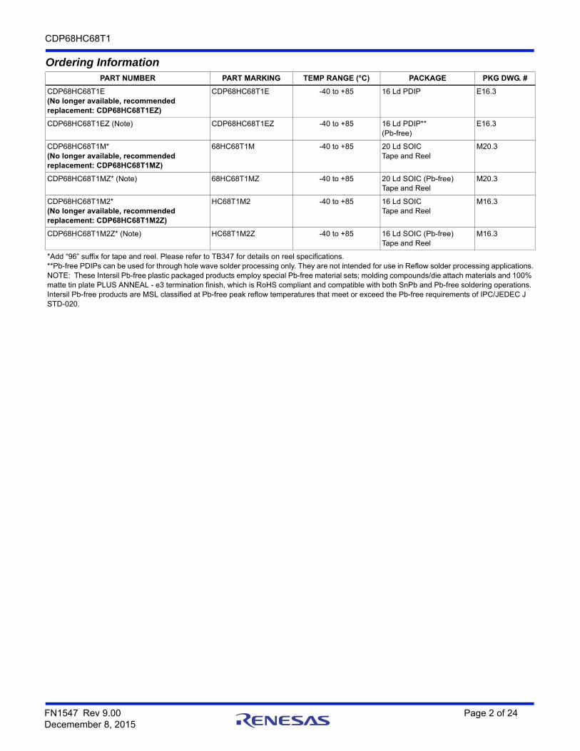
Ordering InformationPART NUMBER PART MARKING TEMP RANGE (°C) PACKAGE PKG DWG. #
CDP68HC68T1E(No longer available, recommendedreplacement: CDP68HC68T1EZ)
CDP68HC68T1E -40 to +85 16 Ld PDIP E16.3
CDP68HC68T1EZ (Note) CDP68HC68T1EZ -40 to +85 16 Ld PDIP**(Pb-free)
E16.3
CDP68HC68T1M*(No longer available, recommended replacement: CDP68HC68T1MZ)
68HC68T1M -40 to +85 20 Ld SOICTape and Reel
M20.3
CDP68HC68T1MZ* (Note) 68HC68T1MZ -40 to +85 20 Ld SOIC (Pb-free)Tape and Reel
M20.3
CDP68HC68T1M2*(No longer available, recommended replacement: CDP68HC68T1M2Z)
HC68T1M2 -40 to +85 16 Ld SOICTape and Reel
M16.3
CDP68HC68T1M2Z* (Note) HC68T1M2Z -40 to +85 16 Ld SOIC (Pb-free)Tape and Reel
M16.3
*Add “96” suffix for tape and reel. Please refer to TB347 for details on reel specifications.**Pb-free PDIPs can be used for through hole wave solder processing only. They are not intended for use in Reflow solder processing applications.NOTE: These Intersil Pb-free plastic packaged products employ special Pb-free material sets; molding compounds/die attach materials and 100% matte tin plate PLUS ANNEAL - e3 termination finish, which is RoHS compliant and compatible with both SnPb and Pb-free soldering operations. Intersil Pb-free products are MSL classified at Pb-free peak reflow temperatures that meet or exceed the Pb-free requirements of IPC/JEDEC J STD-020.
FN1547 Rev 9.00 Page 2 of 24Decemember 8, 2015

CDP68HC68T1
Absolute Maximum Ratings Thermal Information
Supply Voltage (VDD) . . . . . . . . . . . . . . . . . . . . . . . . . . -0.5V to +7VInput Voltage (VIN) . . . . . . . . . . . . . . . . . . . VSS -0.3V to VDD +0.3VCurrent Drain Per Input Pin (Excluding VDD and VSS I) . . . . . 10mACurrent Drain Per Output Pin I. . . . . . . . . . . . . . . . . . . . . . . . . 40mA
Operating ConditionsVoltage Range . . . . . . . . . . . . . . . . . . . . . . . . . . . . . . +3.0V to +6.0VStandby (Timekeeping) Voltage . . . . . . . . . . . . . . . . . +2.2V to +6.0VTemperature Range
CDP68HC68T1E (PDIP Package) . . . . . . . . . . . . .-40°C to +85°CCDP68HC68T1M/M2 (SOIC Packages) . . . . . . . .-40°C to +85°C
Input VoltageInput High . . . . . . . . . . . . . . . . . . . . . . . . . . . . .(0.7 x VDD) to VDDInput Low . . . . . . . . . . . . . . . . . . . . . . . . . . . . . . 0V to (0.3 x VDD)
Serial Clock Frequency (fSCK). . . . . . . . . . . . . . . . . . +3.0V to +6.0V
Thermal Resistance (Typical) JA (°C/W) JC (°C/W)
16 Ld PDIP* (Notes 1, 3) . . . . . . . . . . . 85 3516 Ld SOIC (Notes 2, 3). . . . . . . . . . . . 65 2620 Ld SOIC (Notes 2, 3). . . . . . . . . . . . 60 26
Maximum Junction Temperature (Plastic) . . . . . . . . . . . . . . . +150°CMaximum Storage Temperature Range (TSTG). . . . -65°C to +150°CPb-free Reflow Profile . . . . . . . . . . . . . . . . . . . . . . . . . . . see TB493*Pb-free PDIPs can be used for through hole wave solder processing only. They are not intended for use in Reflow solder processing applications.
CAUTION: Do not operate at or near the maximum ratings listed for extended periods of time. Exposure to such conditions may adversely impact product reliability andresult in failures not covered by warranty.
NOTES:
1. JA is measured with the component mounted on a low effective thermal conductivity test board in free air. See Tech Brief TB379 for details.
2. JA is measured with the component mounted on a high effective thermal conductivity test board in free air. See Tech Brief TB379 for details.
3. For JC, the “case temp” location is taken at the package top center.
Static Electrical Specifications At TA = -40°C to +85°C, VDD = VBATT = 5V ±5%, Unless Otherwise Specified.
PARAMETER SYMBOL TEST CONDITIONS
CDP68HC68T1
UNITSMIN TYP
(Note 4) MAX
Quiescent Device Current IDD - 1 10 µA
Output Voltage High Level VOH IOH = -1.6mA, VDD = 4.5V 3.7 - - V
Output Voltage Low Level VOL IOL = 1.6mA, VDD = 4.5V - - 0.4 V
Output Voltage High Level VOH IOH 10µA, VDD = 4.5V 4.4 - - V
Output Voltage Low Level VOL IOL 10µA, VDD = 4.5V - - 0.1 V
Input Leakage Current IIN - - ±1 µA
Three-State Output Leakage Current IOUT - - ±10 µA
Operating Current (Note 5)(ID + IB) VDD = VB = 5VCrystal Operation
32kHz - 0.08 - mA
1MHz - 0.5 - mA
2MHz - 0.7 - mA
4MHz - 1 - mA
XTAL IN Clock (Squarewave) (Note 5)(ID + IB) VDD = VS = 5V
32kHz - 0.02 0.024 mA
1MHz - 0.1 0.12 mA
2MHz - 0.2 0.24 mA
4MHz - 0.4 0.5 mA
Standby Current (Note 5)VS = 3VCrystal Operation
IB 32kHz - 20 - µA
1MHz - 200 - µA
2MHz - 300 - µA
4MHz - 500 - µA
FN1547 Rev 9.00 Page 3 of 24Decemember 8, 2015

CDP68HC68T1
Operating Current (Note 5)VDD = 5V, VB = 3VCrystal Operation
ID IB - mA
32kHz - 0.025 0.015 - mA
1MHz - 0.08 0.15 - mA
2MHz - 0.15 0.25 - mA
4MHz - 0.3 0.4 - mA
Standby Current (Note 5)VB = 2.2VCrystal Operation
IB 32kHz - 10 - µA
Input Capacitance CIN VIN = 0, TA = +25°C - - 2 pF
Maximum Rise and Fall Times(Except XTAL Input and POR Pin 10)
tr, tf - - 2 µs
- - µs
Input Voltage (Line Input Pin Only, Power Sense Mode)
0 10 12 V
VSYS > VBVT(For VB Not Internally Connected to VDD)
- 1.0 - V
Power-On Reset (POR) Pulse Width 100 75 - ns
NOTES:
4. Typical values are for TA = +25°C and nominal VDD.
5. Clock out (Pin 1) disabled, outputs open circuited. No serial access cycles.
Dynamic Electrical Specifications Bus Timing VDD ±10%, VSS = 0VDC, TA = -40°C to +85°C
IDENTIFICATION NUMBER PARAMETER SYMBOL
LIMITS (ALL TYPES)
UNITS
VDD = 3.3V VDD = 5V
MIN MAX MIN MAX
1 Chip Enable Setup Time tEVCV 200 - 100 - ns
2 Chip Enable After Clock Hold Time tCVEX 250 - 125 - ns
3 Clock Width High tWH 400 - 200 - ns
4 Clock Width Low tWL 400 - 200 - ns
5 Data In to Clock Setup Time tDVCV 200 - 100 - ns
7 Clock to Data Propagation Delay tCVDV - 200 - 100 ns
8 Chip Disable to Output High Z tEXQZ - 200 - 100 ns
11 Output Rise Time tr - 200 - 100 ns
12 Output Fall Time tf - 200 - 100 ns
A Data in After Clock Hold Time tCVDX 200 - 100 - ns
B Clock to Data Out Active tCVQX - 200 - 100 ns
C Clock Recovery Time tREC 200 - 200 - ns
Static Electrical Specifications At TA = -40°C to +85°C, VDD = VBATT = 5V ±5%, Unless Otherwise Specified. (Continued)
PARAMETER SYMBOL TEST CONDITIONS
CDP68HC68T1
UNITSMIN TYP
(Note 4) MAX
FN1547 Rev 9.00 Page 4 of 24Decemember 8, 2015

FN
154
7R
ev 9
.00
Pag
e 5 of 24
De
cem
em
ber 8, 2
015
CD
P6
8HC
68T
1
AY/DAYF WEEK
LENDARLOGIC
MONTH
YEAR
CD
P68H
C68T
1
Functional Block Diagram
FREEZECIRCUIT
CE
LINE
50/60Hz
AM - PM ANDHOUR LOGIC
DOOSCILLATOR
XTAL IN
XTAL OUT
VBATT
PRESCALE SECOND MINUTE HOUR
CA
PRESCALESELECT
CLOCKSELECT
CLOCKCONTROLREGISTER
INTERRUPTCONTROLREGISTER
CLOCKANDINT
LOGIC
CLOCKOUT
INT
VDD
VSS
POWERSENSE
CONTROL
INT STATUSREGISTER
LINE
PSE
VSYS
POR
CPUR
SCK
MISO
MOSI
COMPARATOR
SECONDLATCH
MINUTELATCH
HOURLATCH
32x8RAM
SERIALINTERFACE
8-BIT DATA BUS
FIGURE 1. REAL TIME CLOCK FUNCTIONAL DIAGRAM

CDP68HC68T1
SECONDS
MINUTES
HOURS
DAY OF WEEK
DATE
MONTH
YEARS
NOT USED
SEC ALARM
MIN ALARM
HRS ALARM
NOT USED
NOT USED
NOT USED
NOT USED
NOT USED
STATUS REGISTER
CONTROL REGISTER
INTERRUPT CONTROL REGISTER
32
33
34
35
36
37
38
39
40
41
42
43
44
45
46
47
48
49
50
$20
$21
$22
$23
$24
$25
$26
$27
$28
$29
$2A
$2B
$2C
$2D
$2E
$2F
$30
$31
$32
CLOCK/CALENDAR
13 BYTES UNUSED
TEST MODE
32 RAM LOCATIONS
$00
$1F
$20
$32
$33
$3F
$5585
63
51
50
32
31
0
R = READABLE W = WRITABLE
R, W
R, W
R, W
R, W
R, W
R, W
R, W
W
W
W
R
R, W
R, W
FIGURE 2. ADDRESS MAP
TABLE 1. CLOCK/CALENDAR AND ALARM DATA MODES
ADDRESS LOCATION (H) FUNCTION DECIMAL RANGE BCD DATA RANGEBCD DATE EXAMPLE
(Note 6)
20 Seconds 0 to 59 00 to 59 18
21 Minutes 0 to 59 00 to 59 49
22 Hours12 Hour Mode(Note 7)
1 to 12 81 to 92 (AM)A1 to B2 (PM)
A3
Hours24 Hour Mode
0 to 23 00 to 23 15
23 Day of the Week(Sunday = 1)
1 to 7 01 to 07 03
24 Day of the Month(Date)
1 to 31 01 to 31 29
25 MonthJan = 1, Dec = 12
1 to 12 01 to 12 10
26 Years 0 to 99 00 to 99 85
28 Alarm Seconds 0 to 59 00 to 59 18
29 Alarm Minutes 0 to 59 00 to 59 49
2A Alarm Hours (Note 8)12 Hour Mode
1 to 12 01 to 12 (AM)21 to 32 (PM)
23
Alarm Hours24 Hour Mode
0 to 23 00 to 23 15
NOTES:
6. Example: 3:49:18, Tuesday. Oct. 29,1985.
7. Most significant Bit, D7, is “0” for 24 hours, and “1” for 12 hour mode. Data Bit D5 is “1” for PM and ‘0” for AM in 12 hour mode.
8. Alarm hours. Data Bit D5 is “1” for PM and “0” for AM in 12 hour mode. Data Bits D7 and D6 are DON’T CARE.
FN1547 Rev 9.00 Page 6 of 24Decemember 8, 2015

CDP68HC68T1
Programmers Model - Clock Registers
NAMEWRITE/READ REGISTERSHEX ADDRESS
TENS 0 TO 5
TENS 0 TO 5
12HR24
XPM/AMTENS 0 TO 2
DB7
X X X X
TENS 0 TO 3
TENS 0 TO 1
TENS 0 TO 9
UNITS 0 TO 9
UNITS 0 TO 9
UNITS 0 TO 9
UNITS 1 TO 7
UNITS 0 TO 9
UNITS 0 TO 9
UNITS 0 TO 9
7 6 5 4 3 2 1 0
7 6 5 4 3 2 1 0
WRITE ONLY REGISTERS
TENS 0 TO 5
TENS 0 TO 5
UNITS 0 TO 9
UNITS 0 TO 9
UNITS 0 TO 9PM/AM
TENS 0 TO 2X X
7 6 5 4 3 2 1 0
DB0
SECONDS (00 TO 59)
MINUTES (00 TO 59)
DB7, 1 = 12 HR, 0 = 24 HRDB = 1 PM, 0 = AM
HOURS (01 TO 12 OR 00 TO 23
DATEDAY OF MONTH
MONTH (01 TO 12) JAN = 1DEC = 12
YEARS (00 TO 99)
CONTROL
INTERRUPT
ALARM SECONDS (00 TO 59)
ALARM MINUTES (00 TO 59)
ALARM HOURS (01 TO 12 OR 00 TO 23)PLUS AM/PM IN 12 HR MODE
PM = 1, AM = 0
READ ONLY REGISTERS
STATUS
7 6 5 4 3 2 1 0BIT
HEX ADDRESS 00-1F
20
21
22
23
24
25
26
31
32
28
29
2A
30
RAM DATA BYTE
01 TO 28293031
NOTE: X = Don’t care writes, X = 0 when read.
X DAY OF WK (01 TO 07) SUNDAY = 1
D7 D6 D5 D4 D3 D2 D1 D0
FN1547 Rev 9.00 Page 7 of 24Decemember 8, 2015

CDP68HC68T1
Functional DescriptionThe SPI real-time clock consists of a clock/calendar and a 32x8 RAM. Communications is established via the SPI (Serial Peripheral Interface) bus. In addition to the clock/calendar data from seconds to years, and system flexibility provided by the 32-byte RAM, the clock features computer handshaking with an interrupt output and a separate squarewave clock output that can be one of seven different frequencies. An alarm circuit is available that compares the alarm latches with the seconds, minutes and hours time counters and activates the interrupt output when they are equal. The clock is specifically designed to aid in power-down/power-up applications and offers several pins to aid the designer of battery backup systems.
Mode Select
The voltage level that is present at the VSYS input pin at the end of power-on-reset selects the device to be in the single supply or battery backup mode.
Single-Supply Mode
If VSYS is a logic high when power-on-reset is completed, CLK OUT, PSE and CPUR will be enabled and the device will be completely operational. CPUR will be placed low if the logic level at the VSYS pin goes low. If the output signals CLK OUT, PSE and CPUR are disabled due to a power-down instruction, VSYS brought to a logic low and then to a logic high will re-enable these outputs. An example of the single-supply mode is where only one supply is available and VDD, VBATT and VSYS are tied together to the supply.
Battery Backup Mode
If VSYS is a logic low at the end of power-on-reset, CLK OUT, PSE and CPUR will be disabled (CLK OUT, PSE and CPUR low). This condition will be held until VSYS rises to a threshold (about 1.0V) above VBATT. The outputs CLK OUT, PSE and CPUR will then be enabled and the device will be operational. If VSYS falls below a threshold above VBATT the outputs CLK OUT, PSE and CPUR will be disabled. An example of battery backup operation occurs if VSYS is tied to VDD and VDD is not connected to a supply when a battery is connected to the VBATT pin. (See "Functional Description", VBATT for Battery Backup Operation on page 11.)
Clock/Calendar (See Figures 1 and 2)
The clock/calendar portion of this device consists of a long string of counters that is toggled by a 1Hz input. The 1Hz input is generated by a prescaler driven by an on-board oscillator that utilizes one of four possible external crystals or that can be driven by an external clock source. The 1Hz trigger to the counters can also be supplied by a 50Hz or 60Hz input source that is connected to the LINE input pin.
The time counters offer seconds, minutes and hours data in 12 hour or 24 hour format. An AM/PM indicator is available that once set, toggles every 12 hours. The calendar counters consist of day (day of week), date (day of month), month and
years information. Data in the counters is in BCD format. The hours counter utilizes BCD for hour data plus bits for 12/24 hour and AM/PM. The seven time counters are accessed serially at addresses 20H through 26H. See Table 1.
RAM
The real-time clock also has a static 32x8 RAM that is located at addresses 00-1FH. Transmitting the address/control word with Bit 5 low selects RAM access. Bits 0 through 4 select the RAM location.
Alarm
The alarm is set by accessing the three alarm latches and loading the required data. The alarm latches consist of seconds, minutes and hours registers. When their outputs equal the values in the seconds, minutes and hours time counters, an interrupt is generated. The interrupt output will go low if the alarm bit in the Interrupt Control Register is set high. The alarm interrupt bit in the Status Register is set when the interrupt occurs (see "Functional Description", INT Pin on page 10). To preclude a false interrupt when loading the time counters, the alarm interrupt bit should be set low in the Interrupt Control Register. This procedure is not required when the alarm time is set.
Watchdog Function (See Figure 6)
When Bit 7 in the Interrupt Control Register is set high, the Clock’s CE (chip enable) pin must be toggled at a regular interval without a serial data transfer. If the CE is not toggled, the clock will supply a CPU reset pulse and Bit 6 in the Status Register will be set. Typical service and reset times are listed in Table 2.
Clock Out
The value in the three least significant bits of the Clock Control Register selects one of seven possible output frequencies. (See “Clock Control Register” on page 11). This squarewave signal is available at the CLK OUT pin. When power-down operation is initiated, the output is set low.
Control Registers and Status Registers
The operation of the Real-Time Clock is controlled by the Clock Control and Interrupt Control Registers. Both registers are Read-Write Registers. Another register, the Status Register, is available to indicate the operating conditions. The Status Register is a Read only Register.
Power Control
Power control is composed of two operations, Power Sense and Power-Down/Power-Up. Two pins are involved in power sensing, the LINE input pin and the INT output pin. Two additional pins are utilized during power-down/power-up operation. They are the PSE (Power Supply Enable) output pin and VSYS input pin.
TABLE 2.
50Hz 60Hz XTAL
MIN MAX MIN MAX MIN MAX
Service Time - 10ms - 8.3ms - 7.8ms
Reset Time 20 40ms 16.7 33.3ms 15.6 31.3ms
FN1547 Rev 9.00 Page 8 of 24Decemember 8, 2015

CDP68HC68T1
Power Sensing (See Figure 3)
When Power Sensing is enabled (Bit 5 = 1 in Interrupt Control Register), AC transitions are sensed at the LINE input pin. Threshold detectors determine when transitions cease. After a delay of 2.68ms to 4.64ms, plus the external input circuit RC time constant, an interrupt is generated and a bit is set in the Status Register. This bit can then be sampled to see if system power has turned back on. See "Functional Description", Line pin on page 10. The power-sense circuitry operates by sensing the level of the voltage presented at the line input pin. This voltage is centered around VDD and as long as it is either plus or minus a threshold (about 1V) from VDD a power-sense failure will not be indicated. With an AC signal present, remaining in this VDD window longer than a minimum of 2.68ms will activate the power-sense circuit. The larger the amplitude of the AC signal, the less time it spends in the VDD window, and the less likely a power failure will be detected. A 60Hz, 10VP-P sinewave voltage is an applicable
signal to present at the LINE input pin to setup the power sense function.
Power-Down (See Figure 4)
Power-down is a processor-directed operation. A bit is set in the Interrupt Control Register to initiate operation. Three pins are affected. The PSE (Power Supply Enable) output, normally high, is placed low. The CLK OUT is placed low. The CPUR output, connected to the processors reset input is also placed low. In addition, the Serial Interface is disabled.
Power-Up (See Figures 5 and 6)
Two conditions will terminate the Power-Down mode.
1. The first condition (see Figure 5) requires an interrupt. The interrupt can be generated by the alarm circuit, the programmable periodic interrupt signal, or the power sense circuit.
FIGURE 3. POWER-SENSING FUNCTIONAL DIAGRAM
FIGURE 4. POWER-DOWN FUNCTIONAL DIAGRAM FIGURE 5. POWER-UP FUNCTIONAL DIAGRAM (INITIATED BY INTERRUPT SIGNAL
XTAL IN
XTAL OUT
LINE
VDD REAL-TIME CLOCKCDP68HC68T1
STATUS REGISTER
INT INT
CPUCDP68HC05C16B
VDD
0V
I
VSYS
INTERRUPTCONTROLREGISTER
I
SERIALINTERFACE
CLKOUT
CPUR
REAL-TIME CLOCKCDP68HC68T1
PSE
OSC
RESET
CPUCDP68HC05C4B
MISO
MOSI
FROM SYSTEMPOWER
TO SYSTEMPOWER CONTROL
POWERSENSE
ORALARMCIRCUIT
SERIALINTERFACE
PERIODICINTERRUPT
SIGNAL
POWER-UP
REAL-TIME CLOCKCDP68HC68T1
PSE
CPUR
CLKOUT
INTMISO
MOSI
FN1547 Rev 9.00 Page 9 of 24Decemember 8, 2015

CDP68HC68T1
2. The second condition that releases Power-Down occurs when the level on the VSYS pin rises about 1.0V above the level at the VBATT input, after previously falling to the level of VBATT (see Figure 6) in the Battery Backup Mode or VSYS falls to logic low and returns high in the Single Supply Mode.
CLK OUT
Clock output pin. One of seven frequencies can be selected (or this output can be set low) by the levels of the three LSB’s in the Clock-Control Register. If a frequency is selected, it will toggle with a 50% duty cycle except 2Hz in the 50Hz time base mode. (e.g. if 1Hz is selected, the output will be high for 500ms and low for the same period). During power-down operation (Bit 6 in Interrupt Control Register is set to “1”), the clock-output pin will be set low.
CPUR
CPU reset output pin. This pin functions as an N-Channel only, open-drain output and requires an external pull-up resistor.
INT
Interrupt output pin. This output is driven from a single NFET pulldown transistor and must be tied to an external pull-up resistor. The output is activated to a low level when:
1. Power-sense operation is selected (B5 = 1 in Interrupt Control Register) and a power failure occurs.
2. A previously set alarm time occurs. The alarm bit in the Status Register and interrupt-out signal are delayed 30.5µs when 32kHz operation is selected and 15.3µs for 2MHz and 7.6µs for 4MHz.
3. A previously selected periodic interrupt signal activates.
The Status Register must be read to set the Interrupt output high after the selected periodic interval occurs. This is also true when conditions 1 and 2 activate the interrupt. If power-down had been previously selected, the interrupt will also reset the power-down functions.
SCK, MOSI, MISO
See “Serial Peripheral Interface (SPI)” on page 8.
CE
A positive chip-enable input. A low level at this input holds the serial interface logic in a reset state. This pin is also used for the watchdog function.
VSSThe negative power-supply pin that is connected to ground.
PSE
Power-supply enable output pin. This pin is used to control power to the system. The pin is set high when:
1. VSYS rises above the VBATT voltage after VSYS was placed low by a system failure.
2. An interrupt occurs.
3. A power-on reset (if VSYS is a logic high).
The PSE pin is set low by writing a high into bit 6 (power-down bit) in the Interrupt Control Register.
POR
Power-on reset. A Schmitt-trigger input that generates a power-on internal reset signal using an external RC network. Both control registers and frequency dividers for the oscillator and line input are reset. The Status Register is reset except for the first time up bit (B4), which is set. Single supply or battery backup operation is selected at the end of POR.
LINE
This input is used for two functions. When not used it should be connected to VDD via a 10k resistor. The first function utilizes the input signal as the frequency source for the timekeeping counters. This function is selected by setting Bit 6 in the Clock Control Register. The second function enables the line input to sense a power failure. Threshold detectors operating above and below VDD sense an AC voltage loss. Bit 5 must be set to “1” in the Interrupt Control Register and crystal or external clock source operation is required. Bit 6 in the Clock Control Register must be low to select XTAL operation.
Oscillator Circuit
The CDP68HC68T1 has an on-board 150k resistor that is switched in series with its internal inverter when 32kHz is selected via the Clock Control Register. Note: When first powered up the series resistor is not part of the oscillator circuit. (The CDP68HC68T1 sets up for a 4MHz oscillator).
MISO
VBATT
REAL-TIME CLOCK
PSE
CPUR
CLKOUT
SERIALINTERFACE
VSYS
CDP68HC68T1
MOSI
FIGURE 6. POWER-UP FUNCTIONAL DIAGRAM (INITIATED BY A RISE IN VOLTAGE ON THE “VSYS” PIN)
FN1547 Rev 9.00 Page 10 of 24Decemember 8, 2015

CDP68HC68T1
VSYSThis input is connected to the system voltage. After the CPU initiates power down by setting Bit 6 in the Interrupt Control Register to “1”, the level on this pin will terminate power down if it rises about 1.0V above the level at the VBATT input pin after previously falling below VBATT +1.0V. When power-down is terminated, the PSE pin will return high and the Clock Output will be enabled. The CPUR output pin will also return high. The logic level present at this pin at the end of POR determines the CDP68HC68T1’s operating mode.
VBATTThe oscillator power source. The positive terminal of the battery should be connected to this pin. When the level on the VSYS pin falls below VBATT +1.0V, the VBATT pin will be internally connected to the VDD pin. When the voltage on VSYS rises a threshold above (1.0V) the voltage on VBATT, the connection from VBATT to the VDD pin is opened. When the “LINE” input is used as the frequency source, VBATT may be tied to VDD or VSS. The “XTAL IN” pin must be at VSS if VBATT is at VSS. If VBATT is connected to VDD, the “XTAL IN” pin can be tied to VSS or VDD.
XTAL IN, XTAL OUT
These pins are connected to a 32,768Hz. 1.048576MHz, 2.097152MHz or 4.194304MHz crystal. If an external clock is used, it should be connected to “XTAL IN” with ‘XTAL OUT” left open.
VDDThe positive power-supply pin.
Clock Control Register
Start-Stop
A high written into this bit will enable the counter stages of the clock circuitry. A low will hold all bits reset in the divider chain from 32Hz to 1Hz. A clock out selected by Bit 0, Bit 1 and Bit 2 will not be affected by the stop function except the 1Hz and 2Hz outputs.
Line-XTAL
When this bit is set high, clock operation will use the 50-cycle or 60-cycle input present at the LINE input pin. When the bit is low, the crystal input will generate the 1Hz time update.
XTAL Select
One of 4 possible crystals is selected by value in these two bits:
0 = 4.194304MHz 2 = 1.048576MHz
1 = 2.097152MHz 3 = 32,768Hz
50Hz to 60Hz
50Hz is selected as the line input frequency when this bit is set high. A low will select 60Hz. The power-sense bit in the Interrupt Control Register must be set low for line frequency operation.
Clock Out
The three bits specify one of the 7 frequencies to be used as the squarewave clock output:
0 = XTAL 4 = Disable (low output)1 = XTAL/2 5 = 1Hz2 = XTAL/4 6 = 2Hz3 = XTAL/8 7 = 50Hz or 60Hz
XTAL Operation = 64Hz
All bits are reset by a power-on reset. Therefore, the XTAL is selected as the clock output at this time.
Interrupt Control Register
Watchdog
When this bit is set high, the watchdog operation will be enabled. This function requires the CPU to toggle the CE pin periodically without a serial-transfer requirement. In the event this does not occur, a CPU reset will be issued. Status Register must be read before re-enabling watchdog.
Power-Down
A high in this location will initiate a power down. A CPU reset will occur, the CLK OUT and PSE output pins will be set low and the serial interface will be disabled.
Power Sense
This bit is used to enable the line input pin to sense a power failure. It is set high for this function. When power sense is selected, the input to the 50Hz to 60Hz prescaler is disconnected. Therefore, crystal operation is required when power sense is enabled. An interrupt is generated when a power failure is sensed and the power sense and Interrupt True bit in the Status Register are set. When power sense is activated, a “0” must be written to this location followed by a “1” to re-enable power sense.
XTALIN
22MT1
XTALOUT
R (
NO
TE
8)
CR
YS
TAL
C210pF TO 40pF
C1
5pF TO 30pF
NOTES:
9. All frequencies recommended oscillator circuit. C1, C2 values crystal dependent.
10. R is used for 32KHz operation only. 100k to 300k range as specified by crystal manufacturer.
FIGURE 7. OSCILLATOR CIRCUIT
FN1547 Rev 9.00 Page 11 of 24Decemember 8, 2015

CDP68HC68T1
Alarm
The output of the alarm comparator is enabled when this bit is set high. When a comparison occurs between the seconds, minutes and hours time and alarm counters, the interrupt output is activated. When loading the time counters, this bit should be set low to avoid a false interrupt. This is not required when loading the alarm counters. See "Functional Description", INT for explanation of alarm delay on page 10.
Periodic Select
The value in these 4 bits will select the frequency of the periodic output. (See Table 3).
CLOCK CONTROL REGISTER (Write/Read) - Address 31H
D7 D6 D5 D4 D3 D2 D1 D0
START LINE XTAL XTAL 50Hz CLK OUT CLK OUT CLK OUT
SEL SEL
STOP XTAL 1 0 60Hz 2 1 0
INTERRUPT CONTROL REGISTER (Write/Read) - Address 32H
D7 D6 D5 D4 D3 D2 D1 D0
WATCHDOG POWERDOWN
POWERSENSE
ALARM PERIODIC SELECT
NOTE: All bits are reset by power-on reset.
TABLE 3. PERIODIC INTERRUPT OUTPUT
D0 - D3 VALUEPERIODIC INTERRUPTOUTPUT FREQUENCY
FREQUENCY TIME BASE
XTAL LINE
0 Disable
1 2048Hz X
2 1024Hz X
3 512Hz X
4 256Hz X
5 128Hz X
6 64Hz X
50Hz or 60Hz X
7 32Hz X
8 16Hz X
9 8Hz X
10 4Hz X
11 2Hz X X
12 1Hz X X
13 Minute X X
14 Hour X X
15 Day X X
FN1547 Rev 9.00 Page 12 of 24Decemember 8, 2015

CDP68HC68T1
Watchdog
If this bit is set high, the watchdog circuit has detected a CPU failure.
Test Mode
When this bit is set high, the device is in the TEST MODE.
First-time Up
Power-on reset sets this bit high. This signifies that data in the RAM and Clock is not valid and should be initialized.
Interrupt True
A high in this bit signifies that one of the three interrupts (Power Sense, Alarm, and Clock) is valid.
Power-sense Interrupt
This bit set high signifies that the power-sense circuit has generated an interrupt.
Alarm Interrupt
When the seconds, minutes and hours time and alarm counter are equal, this bit will be set high. Status Register must be read before loading Interrupt Control Register for valid alarm indication after alarm activates.
Clock Interrupt
A periodic interrupt will set this bit high.
All bits are reset by a power-on reset except the “FIRST- TIME UP” which is set. All bits except the power-sense bit are reset after a read of this register.
Pin Signal Description
SCK (Serial Clock Input) (Note 13)
This input causes serial data to be latched from the MOSI input and shifted out on the MISO output.
MOSI (Master Out/Slave In) (Note 13)
Data bytes are shifted in at this pin, most significant bit (MSB) first.
MISO (Master In/Slave Out)
Data bytes are shifted out at this pin, most significant bit (MSB) first.
CE (Chip Enable) (Note 14)
A positive chip-enable input. A low level at this input holds the serial interface logic in a reset state, and disables the output driver at the MISO pin.
NOTES:
13. These inputs will retain their previous state if the line driving them goes into a High-Z state.
14. The CE input has as internal pull-down device, if the input is in a low state before going to High Z, the input can be left in a High Z.
STATUS REGISTER (Read Only) - Address 30H
D7 D6 D5 D4 D3 D2 D1 D0
0 WATCHDOG TESTMODE
FIRSTTIMEUP
INTERRUPTTRUE
POWERSENSE
INTERRUPT
ALARMINTERRUPT
CLOCKINTERRUPT
TRUTH TABLE
MODE
SIGNAL
CE SCK (Note 11) MOSI MISO
DISABLERESET
L INPUT DISABLED INPUT DISABLED HIGH Z
WRITE H CPOL = 1
CPOL = 0
DATA BIT LATCH HIGH Z
READ H CPOL = 1
CPOL = 0
X NEXT DATA BITSHIFTED OUT
(Note 12)
NOTES:
11. When interfacing to CDP68HC05 microcontrollers, serial clock phase bit, CPHA, must be set = 1 in the microcomputer’s Control Register.
12. MISO remains at a high Z until 8-bits of data are ready to be shifted out during a READ. It remains at a high Z during the entire WRITE cycle.
FN1547 Rev 9.00 Page 13 of 24Decemember 8, 2015
CDP68HC68T1
Functional DescriptionThe Serial Peripheral Interface (SPI) utilized by the CDP68HC68T1 is a serial synchronous bus for address and data transfers. The clock, which is generated by the microcomputer is active only during address and data transfers. In systems using the CDP68HC05C4 or CDP68HC05D2, the inactive clock polarity is determined by the CPOL bit in the microcomputer’s Control Register. A unique feature of the CDP68HC68T1 is that it automatically determines the level of the inactive clock by sampling SCK when CE becomes active (see Figure 8). Input data (MOSI) is latched internally on the internal strobe edge and output data (MISO) is shifted out on the shift edge, as defined by Figure 8. There is one clock for each data bit transferred (address, as well as data bits are transferred in groups of 8).
Address and Data FormatThere are three types of serial transfer:
1. Address Control - Figure 9.
2. READ or WRITE Data - Figure 10.
3. Watchdog Reset (actually a non-transfer) Figure 11.
The Address/Control and Data bytes are shifted MSB first, Into the serial data input (MOSI) and out of the serial data output (MISO).
Any transfer of data requires an Address/Control byte to specify a Write or Read operation and to select a Clock or RAM location, followed by one or more bytes of data.
Data is transferred out of MISO for a Read and into MOSI for a Write operation.
Address/Control Byte - (see Figure 9)
It is always the first byte received after CE goes true. To transmit a new address, CE must first go false and then true again. Bit 5 is used to select between Clock and RAM locations.
SHIFTINTERNALSTROBE
INTERNALSTROBESHIFT
CE
SCK
CPOL = 1
SCK
CE
CPOL = 0
MOSI MSB MSB -1
NOTE: “CPOL” is a bit that is set in the microcomputer’s ControlRegister.
FIGURE 8. SERIAL RAM CLOCK (SCK) AS A FUNCTION OF MCU CLOCK POLARITY (CPOL)
BIT 7 6 5 4 3 2 1 0
W/R 0 CLK RAM A4 A3 A2 A1 A0
04 A0 through A4 Selects 5-bit HEX Address of RAM or specifies Clock Register. Most Significant Address Bit. If equal to “1”, A0 through A4 selects a Clock Register. If equal to “0”, A0 through A4 selects one of 32 RAM locations. Must be set to ”0” when not in Test Mode 7W/R W/R = “1” initiates one or more WRITE cycles.W/R = “0”, initiates one or more READ cycles.
5 CLK RAM
6 0
7 W/R
NOTE: SCK can be either polarity.
FIGURE 9. ADDRESS/CONTROL BYTE-TRANSFER WAVEFORMS
A2 A1 A0A3A4CLOCK
0W/RMOSIRAM
SCK (NOTE)
CE
FN1547 Rev 9.00 Page 14 of 24Decemember 8, 2015
CDP68HC68T1
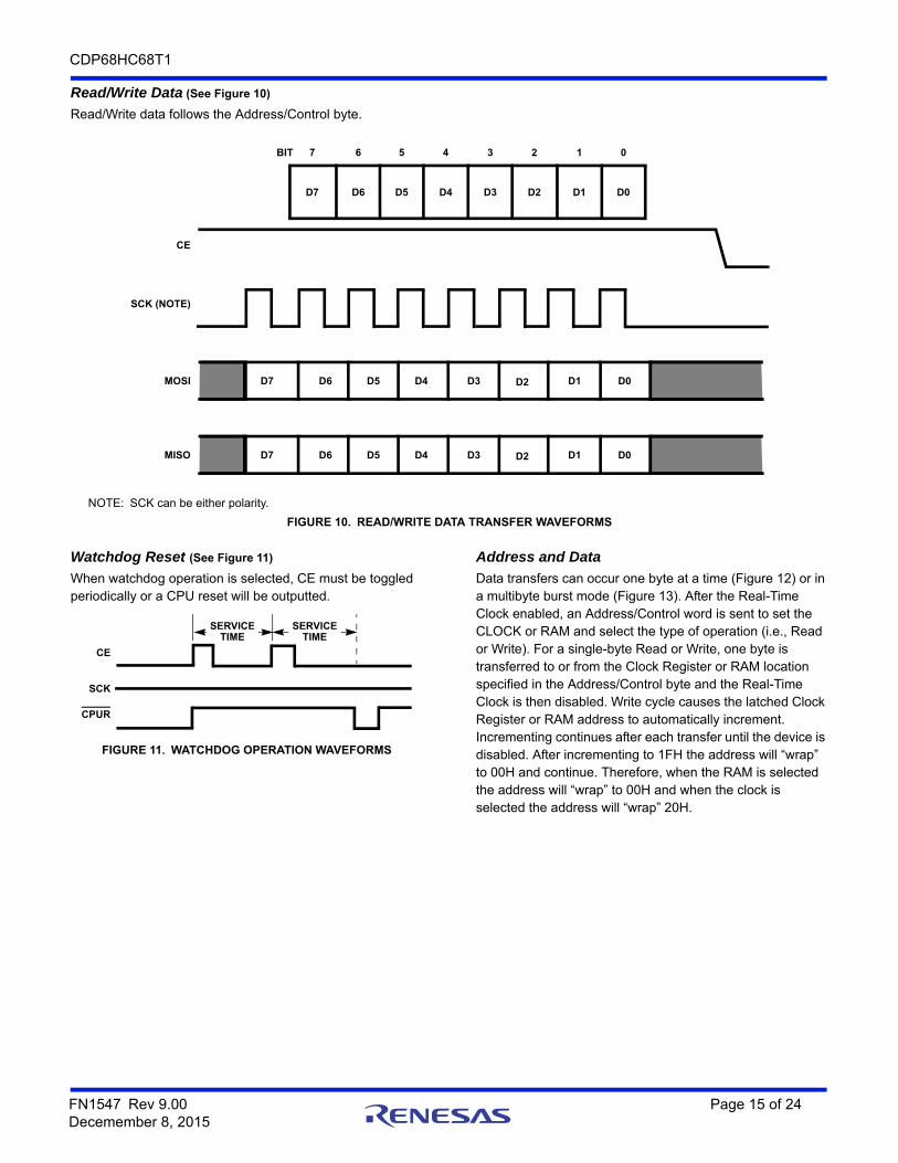
Read/Write Data (See Figure 10)
Read/Write data follows the Address/Control byte.
Watchdog Reset (See Figure 11)
When watchdog operation is selected, CE must be toggled periodically or a CPU reset will be outputted.
Address and Data
Data transfers can occur one byte at a time (Figure 12) or in a multibyte burst mode (Figure 13). After the Real-Time Clock enabled, an Address/Control word is sent to set the CLOCK or RAM and select the type of operation (i.e., Read or Write). For a single-byte Read or Write, one byte is transferred to or from the Clock Register or RAM location specified in the Address/Control byte and the Real-Time Clock is then disabled. Write cycle causes the latched Clock Register or RAM address to automatically increment. Incrementing continues after each transfer until the device is disabled. After incrementing to 1FH the address will “wrap” to 00H and continue. Therefore, when the RAM is selected the address will “wrap” to 00H and when the clock is selected the address will “wrap” 20H.
D7 D6 D5 D4 D3 D2 D1 D0
7 6 5 4 3 2 1 0BIT
D2 D1 D0D3D4D5D6D7
D2 D1 D0D3D4D5D6D7
CE
SCK (NOTE)
MOSI
MISO
NOTE: SCK can be either polarity.
FIGURE 10. READ/WRITE DATA TRANSFER WAVEFORMS
CE
SERVICETIME
SERVICETIME
SCK
CPUR
FIGURE 11. WATCHDOG OPERATION WAVEFORMS
FN1547 Rev 9.00 Page 15 of 24Decemember 8, 2015

CDP68HC68T1
FIGURE 12. SINGLE-BYTE TRANSFER WAVEFORMS
FIGURE 13. MULTIPLE-BYTE TRANSFER WAVEFORMS
CE
SCK
MOSIWRITE
READ
MOSI
MISO READ DATA
ADDRESS BYTE
ADDRESS BYTE WRITE DATA
DATA BYTEWRITE DATA BYTE
CE
SCK
DATA BYTEADDRESS BYTE
MOSI
DATA BYTE
DATA BYTE +1W/R ADDRESS
ADDRESS BYTE
MOSI
MISO
READ
DATA BYTE + (n-1)
DATA BYTEDATA BYTEDATA BYTE
FN1547 Rev 9.00 Page 16 of 24Decemember 8, 2015
CDP68HC68T1
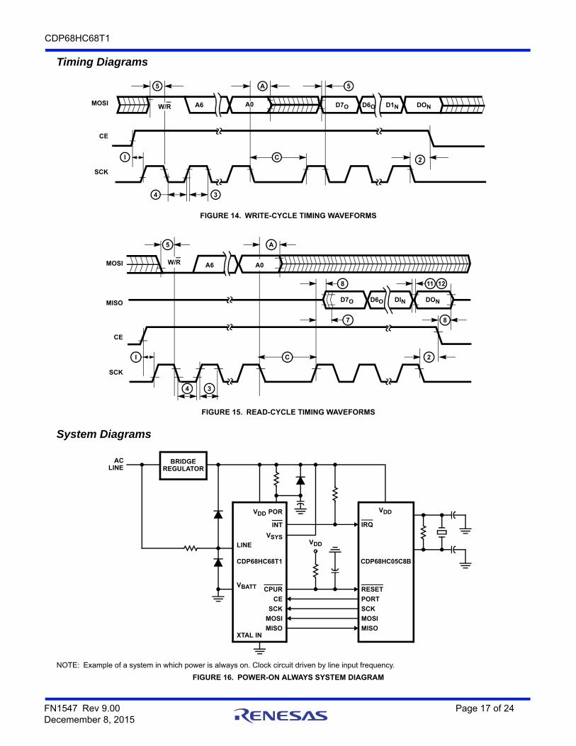
Timing Diagrams
FIGURE 14. WRITE-CYCLE TIMING WAVEFORMS
FIGURE 15. READ-CYCLE TIMING WAVEFORMS
5 A 5
I 2
34
C
MOSI
CE
SCK
W/R A6 A0 D7O D6O D1N DON
12118
A5
7 8
2CI
4 3
MOSI
MISO
CE
SCK
W/R A6 A0
D7O D6O DIN DON
System Diagrams
NOTE: Example of a system in which power is always on. Clock circuit driven by line input frequency.
FIGURE 16. POWER-ON ALWAYS SYSTEM DIAGRAM
VDD
IRQ
CDP68HC05C8B
RESET
PORT
SCK
MOSI
MISO
PORVDD
INT
VSYSLINE
CDP68HC68T1
CE
VBATT CPUR
SCK
MOSI
MISOXTAL IN
BRIDGEREGULATOR
VDD
ACLINE
FN1547 Rev 9.00 Page 17 of 24Decemember 8, 2015

CDP68HC68T1
NOTE: Example of a system in which the power is controlled by an external source. The LINE input pin can sense when the switch opens by use of the POWER-SENSE INTERRUPT. The CDP68HC68T1 crystal drives the clock input to the CPU using the CLK OUT pin. On power down when VSYS < VBATT + 1.0V. VBATT will power the CDP68HC68T1. A threshold detect activates a P-Channel switch, connecting VBATT to VDD. VBATT always supplies power to the oscillator, keeping voltage frequency variation to a minimum.
FIGURE 17. EXTERNALLY CONTROLLED POWER SYSTEM DIAGRAM
A Procedure for Power-Down Operation might consist of the following:
1. Set power sense operation by writing Bit 5 high in the Interrupt Control Register.
2. When an interrupt occurs, the CPU reads the Status Register to determine the interrupt source.
3. Sensing a power failure, the CPU does the necessary housekeeping to prepare for shutdown.
4. The CPU reads the Status Register again after several milliseconds to determine validity of power failure.
5. The CPU sets power-down Bit 6 and disables all interrupts in the Interrupt Control Register when power down is verified. This causes the CPU reset and clock out to be held low and disconnects the serial interface.
6. When power returns and VSYS rises above VBATT, power-down is terminated. The CPU reset is released and serial communication is established.
System Diagrams (Continued)
POR
VDD
VSYS
LINE
CDP68HC68T1
CE
CPUR
MISO
MOSI
SCK
VBATT
CLK OUT
INT
VDD
CDP68HC05C8B
PORT (e.g., PCO)
RESET
MISO
MOSI
SCK
OSC 1
IRQ
BRIDGEGENERATOR
ACLINE
VDD
VDD
FN1547 Rev 9.00 Page 18 of 24Decemember 8, 2015

CDP68HC68T1
FIGURE 18. EXAMPLE OF A SYSTEM WITH A BATTERY BACKUP
System Diagrams (Continued)
ACLINE REGULATOR
POR VDD VSYSVBATT
PSE
CPUR
INT
CLK
XTAL
LINE
OUT
CE
SPIVSS
20k
1k
0.047
VDDRTC
22
M
RCHARGE
0.1
100k
VDD
3
NC
VDD
RESET
CDP68HC05C4B
IRQ
OSC1
PORT
SPI VSS
(EPS)ENABLEDPOWERSUPPLY
FN1547 Rev 9.00 Page 19 of 24Decemember 8, 2015

CDP68HC68T1
Example of an automotive system. The VSYS and LINE inputs can be used to sense the ignition turning on and off. An external switch is included to activate the system without turning on the ignition. Also, the CMOS CPU is not powered down with the system VDD, but is held in a low power reset mode during power down. When restoring power the CDP68HC68T1 will enable the CLK OUT pin and set the PSE and CPUR high.
Important Application Note: Those units with a code of 6PG have delayed alarm interrupts of 8.3ms regardless of CDP68HC68T1’s operating frequency. (See "Functional Description", INT on page 10.) In addition, reading the Status Register before delayed alarm activates will disable alarm signal.
FIGURE 19. AUTOMOTIVE SYSTEM DIAGRAM
System Diagrams (Continued)
XTAL
LINE VDD VSYSVBATT
POR
2MHz
PSE
CPUR
CLK OUT
SPI
CE
INT
T1
VSS
VDD
RESET
OSC1
IRQ
SPI
PORT
CDP68HC05C4B
VSS
PORT
5VREG
+
-
12V
IGNITION
3
CLOCK BUTTON ENABLED POWER
FN1547 Rev 9.00 Page 20 of 24Decemember 8, 2015
CDP68HC68T1
About IntersilIntersil Corporation is a leading provider of innovative power management and precision analog solutions. The company's products address some of the largest markets within the industrial and infrastructure, mobile computing and high-end consumer markets.
For the most updated datasheet, application notes, related documentation and related parts, please see the respective product information page found at www.intersil.com.
You may report errors or suggestions for improving this datasheet by visiting www.intersil.com/ask.
Reliability reports are also available from our website at www.intersil.com/support
Revision HistoryThe revision history provided is for informational purposes only and is believed to be accurate, but not warranted. Please go to the web to make sure that you have the latest revision.
DATE REVISION CHANGE
December 8, 2015 FN1547.9 Updated Ordering Information Table on page 2.
Page 3: Changed Theta JA values and added Theta JC values:16ld PDIP Theta Ja from 90 to 85. Theta Jc 35 (Notes 1,3)16ld SOIC Theta Ja from 100 to 65. Theta Jc 26 (Notes 2,3)20ld SOIC Theta Ja from 95 to 60. Theta Jc 26 (Notes 2,3)Added Notes 2 and 3Updated Pb-free Reflow Profile link
Added Revision History and About Intersil sections.
Updated POD M20.3 to latest revision. Changes:Top View:
Corrected "7.50 BSC" to "7.60/7.40" (no change from rev 2; error was introduced in conversion)Changed "10.30 BSC" to "10.65/10.00" (no change from rev 2; error was introduced in conversion)
Side View:Changed "12.80 BSC" to "13.00/12.60" (no change from rev 2; error was introduced in conversion)Changed "2.65 max" to "2.65/2.35" (no change from rev 2; error was introduced in conversion)
Changed Note 1 from "ANSI Y14.5M-1982." to "ASME Y14.5M-1994"
Updated to new POD format by moving dimensions from table onto drawing and adding land pattern
FN1547 Rev 9.00 Page 21 of 24Decemember 8, 2015

CDP68HC68T1
FN1547 Rev 9.00 Page 22 of 24Decemember 8, 2015
Dual-In-Line Plastic Packages (PDIP)
NOTES:
1. Controlling Dimensions: INCH. In case of conflict between English and Metric dimensions, the inch dimensions control.
2. Dimensioning and tolerancing per ANSI Y14.5M-1982.
3. Symbols are defined in the “MO Series Symbol List” in Section 2.2 of Publication No. 95.
4. Dimensions A, A1 and L are measured with the package seated in JE-DEC seating plane gauge GS-3.
5. D, D1, and E1 dimensions do not include mold flash or protrusions. Mold flash or protrusions shall not exceed 0.010 inch (0.25mm).
6. E and are measured with the leads constrained to be perpendic-ular to datum .
7. eB and eC are measured at the lead tips with the leads unconstrained. eC must be zero or greater.
8. B1 maximum dimensions do not include dambar protrusions. Dambar protrusions shall not exceed 0.010 inch (0.25mm).
9. N is the maximum number of terminal positions.
10. Corner leads (1, N, N/2 and N/2 + 1) for E8.3, E16.3, E18.3, E28.3, E42.6 will have a B1 dimension of 0.030 - 0.045 inch (0.76 - 1.14mm).
eA-C-
CL
E
eA
C
eB
eC
-B-
E1INDEX
1 2 3 N/2
N
AREA
SEATING
BASEPLANE
PLANE
-C-
D1
B1B
e
D
D1
AA2
L
A1
-A-
0.010 (0.25) C AM B S
E16.3 (JEDEC MS-001-BB ISSUE D)16 LEAD DUAL-IN-LINE PLASTIC PACKAGE
SYMBOL
INCHES MILLIMETERS
NOTESMIN MAX MIN MAX
A - 0.210 - 5.33 4
A1 0.015 - 0.39 - 4
A2 0.115 0.195 2.93 4.95 -
B 0.014 0.022 0.356 0.558 -
B1 0.045 0.070 1.15 1.77 8, 10
C 0.008 0.014 0.204 0.355 -
D 0.735 0.775 18.66 19.68 5
D1 0.005 - 0.13 - 5
E 0.300 0.325 7.62 8.25 6
E1 0.240 0.280 6.10 7.11 5
e 0.100 BSC 2.54 BSC -
eA 0.300 BSC 7.62 BSC 6
eB - 0.430 - 10.92 7
L 0.115 0.150 2.93 3.81 4
N 16 16 9
Rev. 0 12/93

FN1547 Rev 9.00 Page 23 of 24Decemember 8, 2015
CDP68HC68T1
Intersil products are manufactured, assembled and tested utilizing ISO9001 quality systems as notedin the quality certifications found at www.intersil.com/en/support/qualandreliability.html
Intersil products are sold by description only. Intersil may modify the circuit design and/or specifications of products at any time without notice, provided that such modification does not, in Intersil's sole judgment, affect the form, fit or function of the product. Accordingly, the reader is cautioned to verify that datasheets are current before placing orders. Information furnished by Intersil is believed to be accurate and reliable. However, no responsibility is assumed by Intersil or its subsidiaries for its use; nor for any infringements of patents or other rights of third parties which may result from its use. No license is granted by implication or otherwise under any patent or patent rights of Intersil or its subsidiaries.
For information regarding Intersil Corporation and its products, see www.intersil.com
For additional products, see www.intersil.com/en/products.html
© Copyright Intersil Americas LLC 2002-2015. All Rights Reserved.All trademarks and registered trademarks are the property of their respective owners.
Small Outline Plastic Packages (SOIC)
NOTES:
1. Symbols are defined in the “MO Series Symbol List” in Section 2.2 of Publication Number 95.
2. Dimensioning and tolerancing per ANSI Y14.5M-1982.
3. Dimension “D” does not include mold flash, protrusions or gate burrs. Mold flash, protrusion and gate burrs shall not exceed 0.15mm (0.006inch) per side.
4. Dimension “E” does not include interlead flash or protrusions. Interlead flash and protrusions shall not exceed 0.25mm (0.010 inch) per side.
5. The chamfer on the body is optional. If it is not present, a visual index feature must be located within the crosshatched area.
6. “L” is the length of terminal for soldering to a substrate.
7. “N” is the number of terminal positions.
8. Terminal numbers are shown for reference only.
9. The lead width “B”, as measured 0.36mm (0.014 inch) or greater above the seating plane, shall not exceed a maximum value of 0.61mm (0.024inch)
10. Controlling dimension: MILLIMETER. Converted inch dimensions are not necessarily exact.
INDEXAREA
E
D
N
1 2 3
-B-
0.25(0.010) C AM B S
e
-A-
L
B
M
-C-
A1
A
SEATING PLANE
0.10(0.004)
h x 45°
C
H 0.25(0.010) BM M
M16.3 (JEDEC MS-013-AA ISSUE C)16 LEAD WIDE BODY SMALL OUTLINE PLASTIC PACKAGE
SYMBOL
INCHES MILLIMETERS
NOTESMIN MAX MIN MAX
A 0.0926 0.1043 2.35 2.65 -
A1 0.0040 0.0118 0.10 0.30 -
B 0.013 0.0200 0.33 0.51 9
C 0.0091 0.0125 0.23 0.32 -
D 0.3977 0.4133 10.10 10.50 3
E 0.2914 0.2992 7.40 7.60 4
e 0.050 BSC 1.27 BSC -
H 0.394 0.419 10.00 10.65 -
h 0.010 0.029 0.25 0.75 5
L 0.016 0.050 0.40 1.27 6
N 16 16 7
0° 8° 0° 8° -
Rev. 1 6/05
CDP68HC68T1
FN1547 Rev 9.00 Page 24 of 24Decemember 8, 2015
CDP68HC68T1
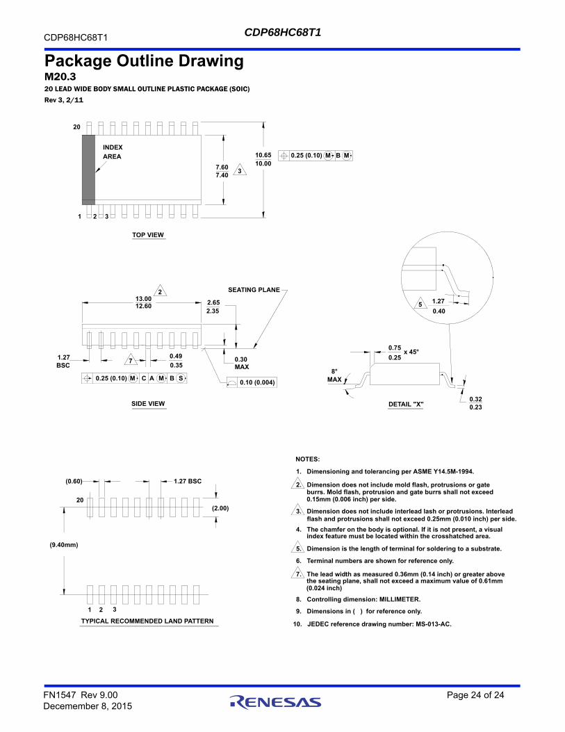
Package Outline DrawingM20.320 LEAD WIDE BODY SMALL OUTLINE PLASTIC PACKAGE (SOIC)
Rev 3, 2/11
7. The lead width as measured 0.36mm (0.14 inch) or greater above the seating plane, shall not exceed a maximum value of 0.61mm
DETAIL "X"SIDE VIEW
TYPICAL RECOMMENDED LAND PATTERN
TOP VIEW
13.00
0.75
0.25x 45°
0.320.23
MAX8°
1.27
0.40
10.6510.00
7.607.40
20
1 2 3
INDEX
AREA
2.652.35
0.30MAXBSC
1.270.35
0.49
0.25 (0.10) M C SBMA0.10 (0.004)
0.25 (0.10) M B M
1 2
1.27 BSC
(9.40mm)
SEATING PLANE
(0.60)
(2.00)
2
20
3
3
5
7
NOTES:
1. Dimensioning and tolerancing per ASME Y14.5M-1994.
2. Dimension does not include mold flash, protrusions or gate
3. Dimension does not include interlead lash or protrusions. Interlead flash and protrusions shall not exceed 0.25mm (0.010 inch) per side.
4. The chamfer on the body is optional. If it is not present, a visual index feature must be located within the crosshatched area.
5. Dimension is the length of terminal for soldering to a substrate.
6. Terminal numbers are shown for reference only.
8. Controlling dimension: MILLIMETER.
9. Dimensions in ( ) for reference only.
burrs. Mold flash, protrusion and gate burrs shall not exceed 0.15mm (0.006 inch) per side.
(0.024 inch)
10. JEDEC reference drawing number: MS-013-AC.
12.60