datasheet - srk1001 - adaptive synchronous rectification ... · converter efficiency at light load,...
TRANSCRIPT

SO8 package Features• Secondary side synchronous rectification controller optimized for flyback
converter• Suitable for QR and mixed CCM/DCM fixed frequency operation• Wide VCC operating voltage range 3.7 to 32 V• CC regulation operation down to 2V output supported• Very low quiescent current in low consumption mode (170 µA)• High-voltage sensing input for SR MOSFET drain-source voltage (185 V AMR)• Operating frequency up to 300 kHz• High-current gate-drive output for N-MOSFET• Fast turn-on with minimum delay time and adaptive turn-off logic• Programmable minimum TON and TOFF
• Low consumption mode entry by DIS pin, by primary side burst-mode detectionor by detection of SR MOSFET conduction lower than programmed min. TON
• SO8 package
Applications• AC-DC adapters• Battery chargers / quick chargers• USB power delivery (profile 4)• Industrial SMPS
DescriptionThe SRK1001 controller is designed for secondary side synchronous rectification(SR) in flyback converters, suitable for operation in QR and mixed CCM/DCM fixedfrequency circuits.
It provides a high-current gate-drive output capable of driving N-channel PowerMOSFETs.
The control scheme of this IC is such that the SR MOSFET is switched on as soon ascurrent starts flowing through its body diode, and then switched off as currentapproaches zero.
The fast turn-on with minimum delay and innovative adaptive turn-off logic allowmaximizing the conduction time of the SR MOSFET and eliminating the effect ofparasitic inductance in the circuit.
The device enters low consumption mode when it detects primary controller burst-mode operation, or when the DIS pin is pulled up by the user, or when the SRMOSFET conduction falls below the programmed minimum TON. This improves theconverter efficiency at light load, where synchronous rectification is no longerbeneficial.
After the converter restarts switching or the DIS pin goes low again and the ICdetects that the current conduction in the rectifiers has increased 20% above the minTON programmed value, the IC exits low consumption mode and resumes switchingoperation.
Product status link
SRK1001
Product summary
Order code SRK1001
Package SO8
Packing Tape and reel
Adaptive synchronous rectification controller for flyback converter
SRK1001
Datasheet
DS13155 - Rev 1 - November 2019For further information contact your local STMicroelectronics sales office.
www.st.com

1 Block diagram and pin connection
Figure 1. Internal block diagram
DRIVER
HV CLAMP COMPARATORS TIMER
ADAPTIVE CONTROL
CONTROL LOGIC
ON ZCD
POWER MANAGEMENT &
SWITCH OVER
GND
TON
DVS
GD
VAUX
VCC
TOFF
DIS/SYNC
Figure 2. Pin connections (top view)
VAUX
TOFF
TON
DVS
SO8
GD
DIS/SYNC
GND
VCC
1
2
3
4 5
6
7
8
Table 1. Pin functions
N. Name Function
1 DIS/SYNC
This pin has two functions: disable and synchronization input.• Asynchronous turn-off of SR MOSFET always occurs after DIS pin voltage shows a positive rising edge
and the synchronous rectification stays disabled as long as it remains at the high level. If the DIS pinvoltage stays high for at least 4 switching cycles, the device enters low consumption mode.
• Synchronization function requires that no external capacitor must be mounted between TON pin and GND,so that SR MOSFET turn-off is accomplished by the positive rising edge of the applied SYNC signal orwhen triggered by ZCD comparator output.
This pin is pulled high by internal current source (5 µA); if not used, it must be grounded.
2 GDGate driver output. Totem pole output stage is able to drive power MOSFET with high peak current levels. Toavoid excessive gate voltages in case the device is supplied with a high VCC, the high level voltage of this pin isclamped to about 11.5 V. The pin must be connected directly to the SR MOSFET gate terminal.
3 GND Return of the device bias current and return of the gate drive current. Route this pin close to the source terminalof synchronous rectifier MOSFET.
SRK1001Block diagram and pin connection
DS13155 - Rev 1 page 2/27
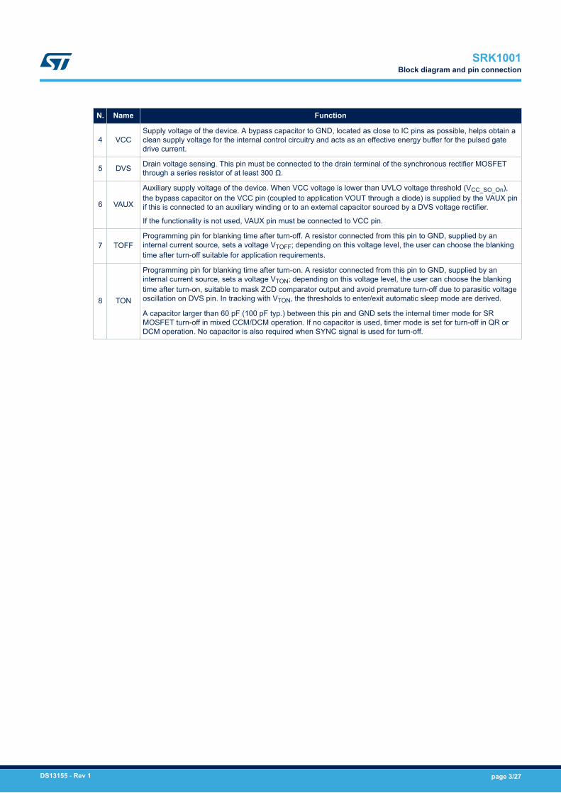
N. Name Function
4 VCCSupply voltage of the device. A bypass capacitor to GND, located as close to IC pins as possible, helps obtain aclean supply voltage for the internal control circuitry and acts as an effective energy buffer for the pulsed gatedrive current.
5 DVS Drain voltage sensing. This pin must be connected to the drain terminal of the synchronous rectifier MOSFETthrough a series resistor of at least 300 Ω.
6 VAUX
Auxiliary supply voltage of the device. When VCC voltage is lower than UVLO voltage threshold (VCC_SO_On),the bypass capacitor on the VCC pin (coupled to application VOUT through a diode) is supplied by the VAUX pinif this is connected to an auxiliary winding or to an external capacitor sourced by a DVS voltage rectifier.
If the functionality is not used, VAUX pin must be connected to VCC pin.
7 TOFFProgramming pin for blanking time after turn-off. A resistor connected from this pin to GND, supplied by aninternal current source, sets a voltage VTOFF; depending on this voltage level, the user can choose the blankingtime after turn-off suitable for application requirements.
8 TON
Programming pin for blanking time after turn-on. A resistor connected from this pin to GND, supplied by aninternal current source, sets a voltage VTON; depending on this voltage level, the user can choose the blankingtime after turn-on, suitable to mask ZCD comparator output and avoid premature turn-off due to parasitic voltageoscillation on DVS pin. In tracking with VTON, the thresholds to enter/exit automatic sleep mode are derived.
A capacitor larger than 60 pF (100 pF typ.) between this pin and GND sets the internal timer mode for SRMOSFET turn-off in mixed CCM/DCM operation. If no capacitor is used, timer mode is set for turn-off in QR orDCM operation. No capacitor is also required when SYNC signal is used for turn-off.
SRK1001Block diagram and pin connection
DS13155 - Rev 1 page 3/27
2 Maximum ratings
Table 2. Absolute maximum ratings
Symbol Pin Parameter Value Unit
VCC 4 DC supply voltage -0.3 to 36 V
DVS 5 Drain sense voltage referred to GND (with 300 Ω in series to the pin) -3 to 185 V
VAUX 6 Auxiliary DC supply voltage -0.3 to 185 V
VTOFF 7 TOFF pin voltage rating -0.3 to 3.6 V
VTON 8 TON pin voltage rating -0.3 to 3.6 V
VSYNC/DIS 1 DIS/SYNC pin voltage rating -0.3 to 3.6 V
Stressing the device above the rating listed in above table may cause permanent damage to the device. Exposureto absolute maximum rated conditions may affect device reliability.
Table 3. Thermal data
Symbol Parameter Value Unit
Θth j-amb Max. thermal resistance, junction-to-ambient(1) 125 °C/W
Ψth j-case Max thermal resistance, junction-to-case top(1) 5 °C/W
Ptot Power Dissipation @Tamb = 50°C 0.8 W
Tj Junction Temperature Operating range -40 to 150 °C
Tstg Storage Temperature -55 to 150 °C
1. Natural convection test environment, using JEDEC 1s1p PCB with vias.
SRK1001Maximum ratings
DS13155 - Rev 1 page 4/27

3 Typical application schematic
Figure 3. Typical application schematic
SRK1001Typical application schematic
DS13155 - Rev 1 page 5/27

4 Electrical characteristics
Tj = -25°C to 125°C, VCC = 12 V, CGD = 4.7 nF; unless otherwise specified, typical values refer to Tj = 25°C
Table 4. Electrical characteristics
Symbol Parameter Test Condition Min. Typ. Max. Unit
Supply section
VAUX VAUX pin operating voltage 185 V
VCC Operating voltage range After turn-on 3.7 32 V
VCC_On Turn-on supply voltage Voltage rising (1) 4.18 4.3 4.42 V
VCC_SO_OnTurn-on supply voltage for AUX switchactivation Voltage falling (1) 3.7 3.95 4.15 V
VCC_Off Turn-off supply voltage Voltage falling (1) 3.3 3.5 3.7 V
VCC_AGD_enVCC voltage above which adaptive drive isenabled
On VCC rising edge (2) 7.4 V
VCC_AGD_disVCC voltage below which adaptive drive isdisabled
On VCC falling edge (2) 6.5 V
Iq_run Current consumption in run mode After turn-on (excluding SR MOSgate driving) @ 100 kHz 600 µA
ICC Operating supply current @ 300 kHz 17 mA
Iq Quiescent CurrentLow consumption mode operation,with DVS pin not switching (3), Tj =-25°C to 85°C
170 225 µA
Ron VAUX switch resistance (2) 40 Ω
IDSAT_VAUX VAUX pin saturation current 125 mA
Drain-source sensing input and synch function
VDS_H DVS operating voltage 185 V
VTH_A Cycle comparator threshold 70 100 130 mV
VZCD_OFF_MIN Minimum ZCD comparator threshold (2) -20 mV
Tdiode_offBody diode residual conduction time after turn-off 230 330 430 ns
TD_On_min Turn-on delay 55 85 105 ns
Tant_timerAnticipation time referred to DVS rising edge toforce turn off of SR MOSFET
DVS switching
Low level on DVS pin = -1 V180 280 325 ns
Ttimer_stepTimer step every 4 switching cycles (in FFoperation)
With 100pF on TON pin, duringswitching period increase 56 ns
TON_MAX Max turn-on duration 45 60 80 µs
Disable pin remote on/off function
VDIS_OFF Disable threshold
For at least 4 cycle to enter indisable state (low consumptionmode).
Used also as SYNCH input, italways forces a SR MOSFET turnoff when pulled high
1.9 2.1 2.3 V
SRK1001Electrical characteristics
DS13155 - Rev 1 page 6/27

Symbol Parameter Test Condition Min. Typ. Max. Unit
VDIS_ON Enable threshold 1.4 1.6 1.8 V
IDIS Sourced current 5 µA
Tmask Sync signal masking time after turn-on 170 ns
ToutTime-out interval from DVS falling, after whichturn-on by sync signal is not allowed 300 ns
Tpulse Minimum sync pulse width to trigger a turn-off 50 ns
Blanking time after turn-on programming
TON_MINMinimum turn-on time programmable by RTONin the range [33 kΩ - 250 kΩ]
RTON_MIN = 33 kΩ 0.28 0.4 0.52µs
RTON_MAX= 250 kΩ 2.1 3.0 3.9
ITON Sourced current In run mode 8 µA
Blanking time after turn off programming
TOFF_MIN
Blanking time after turn-off (with DVS voltagecontinuously above VTH_A) programmable byRTOFF in the range [16 kΩ - 200 kΩ]
RTOFF_MIN = 16 kΩ 0.34 0.48 0.63µs
RTOFF_MAX= 200 kΩ 4.7 6.7 8.7
ITOFF Sourced current Run/Sleep Mode 10 µA
Low consumption mode
TON_sleep_in
Minimum operating current conduction time toenter sleep-mode:
TON_sleep_in = TON_MIN + 300 ns
RTON_MIN = 33 kΩ 0.49 0.7 0.91µs
RTON_MAX= 250 kΩ 2.31 3.3 4.29
TON_sleep_out
Restart current conduction time from sleep-mode:
TON_sleep_out = 1.2*TON_MIN + 300 ns
RTON_MIN = 33 kΩ 0.55 0.78 1µs
RTON_MAX= 250 kΩ 2.73 3.9 5.07
TstopSwitching stop time interval detection to enterlow consumption mode (primary controllerburst-mode)
80 120 160 µs
Gate driver
Isource_pk Output source peak current See (2) 0.6 A
Isink_pk Output sink peak current See (2) 1 A
tr_1 Rise Time (see picture below)VCC = 20V, CGD = 4.7 nF 45
nsVCC = 20V, CGD = 10 nF 75
tr_2 Rise Time (see picture below)VCC = 20V, CGD = 4.7 nF 140
nsVCC = 20V, CGD = 10 nF 140
tf Fall Time (see picture below)VCC = 20V, CGD = 4.7 nF 60 ns
VCC = 20V, CGD = 10 nF 120
VGDclamp Drive clamp voltage VCC = 20V (4) 10.6 11.6 12.6 V
VGD_ad-step Adaptive driving step voltage VCC = 20V (4) 400 mV
VGDL_UVLO UVLO saturation VCC = 0 to VCC_On, Isink = 5 mA 1 1.3 V
1. Parameters tracking each other2. Parameter guaranteed by design3. Low-consumption-mode is one of the following: sleep-mode for conduction below min TON, converter burst-mode detection
or DIS pin pulled high for at least 4 cycles4. Parameters tracking each other
SRK1001Electrical characteristics
DS13155 - Rev 1 page 7/27

Figure 4. Rise and fall time definition
tr_1
tr_2
80% VGDclamp
5 V
VGDclamp
tf
10% VGDclamp
SRK1001Electrical characteristics
DS13155 - Rev 1 page 8/27

5 Operation description
SRK1001 (see Figure 1. Internal block diagram) controller is specifically designed for synchronous rectification inflyback converters operating in QR and mixed CCM/DCM fixed frequency. This IC turns on the SR MOSFET witha minimum delay when the rectified current starts flowing through the body diode, and turns off the SR MOSFETwhen current approaches zero, using an adaptive mechanism that leads the body diode residual conduction timeafter turn-off to the target value Tdiode_off (refer to Table 4 for the various parameter values).The adaptive turn-off method presents certain advantages compared to a standard approach based on acomparator with fixed threshold.The first advantage is that the adaptive method automatically compensates stray inductances LS in series torectified current path: this parasitic (mainly the SR MOSFET package inductances in series to drain and sourceterminals) normally produces an offset on the sensed voltage across MOSFET RDS_ON that anticipates by TX =LS/RDS_ON the turn-off in case of standard comparator.The second aspect to consider is that a standard comparator with fixed threshold turns off at a current level IOFFthat depends on RDS_ON of the chosen SR MOSFET. Referring to Figure 5. Comparison between adaptive turn-off and comparator based turn-off and considering a fixed comparator threshold VTH = -5 mV, the turn-off currentin the rectifier can be calculated.In an application with a SR MOSFET having channel resistance RDS_ON = 2.5 mΩ and package stray inductanceLS = 2.5 nH, where the current slope is di/dt = -3 A/µs (for example starting from a peak current of 15 A with 5 µstransformer demagnetization), the turn off current is:
• IOFF = – VTHRDS_ON – TXdidt = 5A for comparator turn-off
• IOFF_AD = − Tdiode_off*didt = 0.9A for adaptive turn-off
Furthermore, the adaptive turn-off method also performs better in applications with CC regulation, where thestandard comparator with fixed threshold increasingly anticipates the turn-off during load impedance drops (sincecurrent slope also decreases), while the adaptive method fixes Tdiode_off.The SRK1001 controller starts operation when the VCC pin voltage exceeds the turn-on threshold VCC_On; then itstops operation when the VCC voltage drops below the turn-off threshold VCC_Off.In order to guarantee SR switching even with low VCC supply voltage (in the case of chargers operating in CCregulation), the device is provided with the VAUX pin. When the VCC voltage decreases below the thresholdVCC_SO_On (> VCC_Off), an internal switch is turned on, allowing VCC pin capacitor to be charged up to the turn-onthreshold VCC_On by a current drawn through VAUX pin connected, for example, to the rectified SR MOSFETdrain voltage or to another auxiliary voltage of the flyback transformer.For maximum flexibility across all kinds of applications and to overcome noise and ringing problems that mayarise after turn-on and turn-off events, the SRK1001 allows users to program the blanking time after turn-on andafter turn-off by means of two resistors connected between TON and TOFF pins to GND, respectively.
SRK1001Operation description
DS13155 - Rev 1 page 9/27

Figure 5. Comparison between adaptive turn-off and comparator based turn-off
TX = LS / RDS_ON
anticipation on DVS sensing signal due to stray inductance LS
ISR
GD
TD_On
DVS TX
turn-off by comparator and fixed VTH threshold
VTH
IOFF
VZCD_OFF
GD
TD_On
ISR
DVS
targetTdiode_off
(300ns)
TX
adaptive turn-off(VZCD_OFF threshold)
IOFF_AD
5.1 Drain voltage sensing
The drain voltage of the SR MOSFET is sensed through the DVS pin: this is a high voltage pin and needs to beproperly routed to the MOSFET drain, through a resistor of at least 300 Ω (in order to limit dynamic currentinjection in any condition). The DVS signal is used to detect when current flows through the MOSFET body diodeand for the internal timings.
5.2 Turn-on
After the flyback converter primary switch has been turned off, the voltage across the transformer reverses andthe SR MOSFET drain voltage quickly decreases and goes negative (-VF), allowing the rectifier current to flow.Consequently, triggered on the falling edge of the DVS signal (when it decreases below the arming voltageVTH_A), the controller turns on the SR MOSFET, with a very short delay TD_On. After turn-on, the sensed DVSsignal passes from the (negative) body diode forward voltage to the drop across the MOSFET channel resistance(RDS_ON).This drop is generally affected by some amount of noise, associated with the flyback transformer leakageinductance, and this could trigger a premature turn-off of the SR MOSFET.
5.3 Minimum TON programming
In order to avoid premature turn-off of the SR MOSFET due to ringing and oscillations, the IC allows user toprogram a blanking time after turn-on. The circuit bases on an internal timing capacitance and an external resistorRTON connected from TON pin to ground. The blanking time settlement is done according to the followingexpression:TON_MIN = 12*10−12*RTON(with RTON expressed in Ohms and TON_MIN in seconds, starting from when the DVS signal falls below VTH_A).This blanking time sets a minimum turn-on time of the SR MOSFET as well: hence, when load reduction causesthe SR MOSFET conduction time to become shorter than the programmed blanking time, the IC must stop drivingthe SR MOSFET to avoid current inversion (see Section 5.7 Low consumption mode operation: sleep-mode,burst mode, disable state).
5.4 Adaptive turn-off and TIMER
The SR MOSFET can be turned off through two coexisting mechanisms (whichever triggers first), the first basedon an adaptive algorithm, the second on the internal timer.
SRK1001Drain voltage sensing
DS13155 - Rev 1 page 10/27

The adaptive turn-off consists of a ZCD_OFF comparator, where the DVS signal is compared to an adaptingthreshold. This threshold is adapted in such a way that, at steady state, the measured residual conduction time ofSR MOSFET body diode after turn-off meets the target value Tdiode_off (as shown in Figure 6. ZCD_OFFthreshold adapting for target body diode conduction). The residual conduction time of the body diode is measuredbetween the falling edge of the driving signal and the rising edge of the DVS signal (first time exceeding thearming voltage VTH_A).
Figure 6. ZCD_OFF threshold adapting for target body diode conduction
ISRIp
DVS
GD
body diode residual conduction measurement
VTH_A
target Tdiode_off
VZCD_OFFadaptedZCD_OFF threshold
TD_On
The internal timer turns off the SR MOSFET with a fixed anticipation time Tant_timer with respect to the first risingedge of the DVS signal. The IC has two different user timer operating modes optimized for fixed frequency mixedCCM/DCM converters or for QR/DCM applications. The selection of the proper timer mode is performed through a100 pF capacitor across the TON pin:• if capacitor is present, mixed CCM/DCM operation is assumed• if capacitor is not present, QR/DCM operation is assumed.
5.4.1 Fixed frequency mixed DCM/CCM operationIn fixed frequency operation, SR MOSFET turn-off is triggered by ZCD_OFF adaptive mechanism at load levelswhere DCM operation occurs, while it is triggered by timer at higher loads where CCM operation occurs. Thelatter consists of turning off the SR MOSFET with a fixed lead time Tant_timer with respect to the first rising edge ofthe DVS signal, based on a switching period TSW estimate, (over a few previous cycles) as illustrated in Figure 7.Turn-off by the timer may also intervene during low-to-high load transients, where the ZCD_OFF threshold is inthe adapting phase (because of the output voltage drop occurring as a consequence of the transient), preventingundesired current inversions.Most flyback controllers use operating frequency modulation to help optimize the EMI filter. For correct operationof the SRK1000 timer, the maximum rate of change of modulated frequency must be limited, so the switchingperiod increase from the current cycle to the following cycle is much shorter than the timer anticipation Tant_timer(14 ns maximum). In fact, the timer anticipation adaptation during the switching period increase is limited toTtimer_step every 4 cycles, and with a switching period increase longer than 14 ns from one cycle to the next, thetimer turn-off lead time steadily increases (increasing the body diode conduction).
SRK1001Adaptive turn-off and TIMER
DS13155 - Rev 1 page 11/27
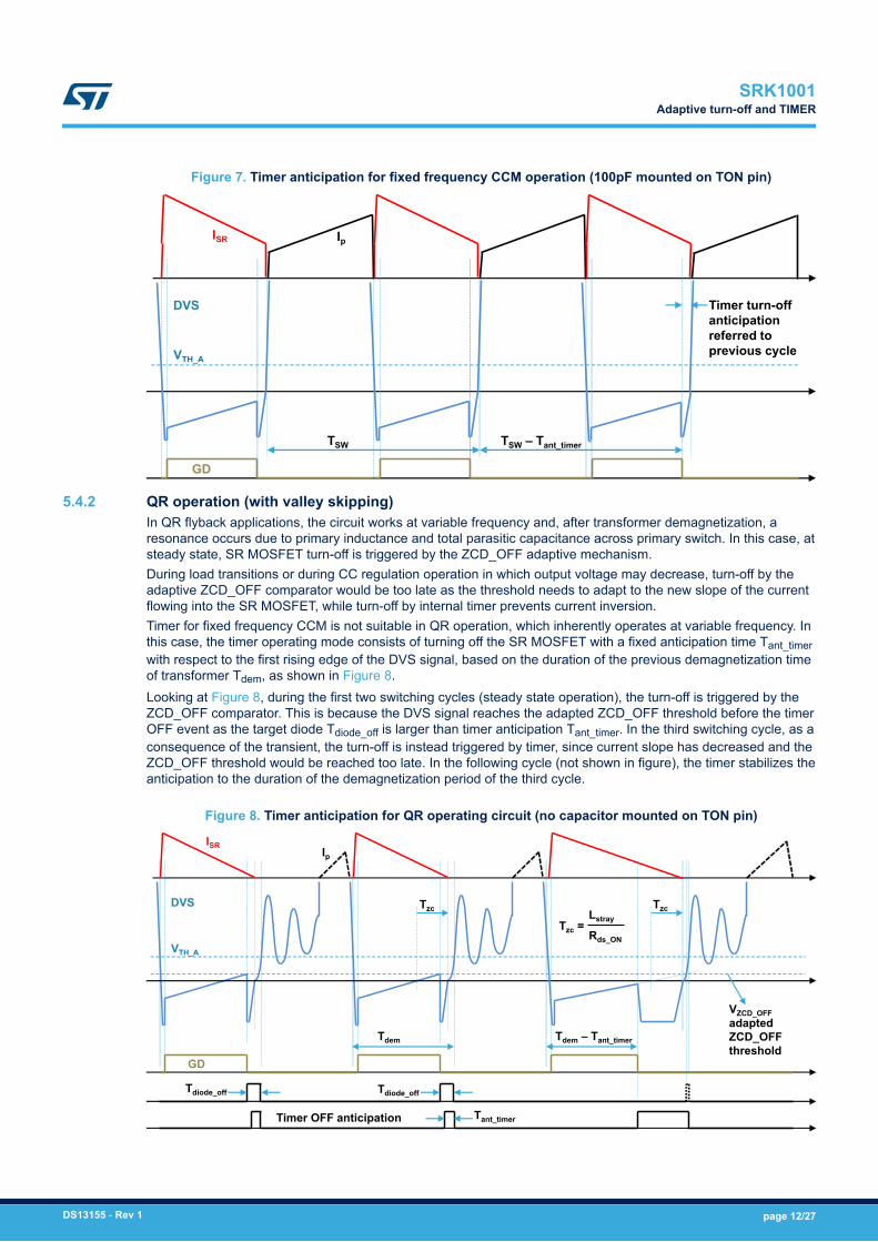
Figure 7. Timer anticipation for fixed frequency CCM operation (100pF mounted on TON pin)
ISR Ip
DVS
GD
VTH_A
TSW TSW – Tant_timer
Timer turn-off anticipationreferred to previous cycle
5.4.2 QR operation (with valley skipping)In QR flyback applications, the circuit works at variable frequency and, after transformer demagnetization, aresonance occurs due to primary inductance and total parasitic capacitance across primary switch. In this case, atsteady state, SR MOSFET turn-off is triggered by the ZCD_OFF adaptive mechanism.During load transitions or during CC regulation operation in which output voltage may decrease, turn-off by theadaptive ZCD_OFF comparator would be too late as the threshold needs to adapt to the new slope of the currentflowing into the SR MOSFET, while turn-off by internal timer prevents current inversion.Timer for fixed frequency CCM is not suitable in QR operation, which inherently operates at variable frequency. Inthis case, the timer operating mode consists of turning off the SR MOSFET with a fixed anticipation time Tant_timerwith respect to the first rising edge of the DVS signal, based on the duration of the previous demagnetization timeof transformer Tdem, as shown in Figure 8.Looking at Figure 8, during the first two switching cycles (steady state operation), the turn-off is triggered by theZCD_OFF comparator. This is because the DVS signal reaches the adapted ZCD_OFF threshold before the timerOFF event as the target diode Tdiode_off is larger than timer anticipation Tant_timer. In the third switching cycle, as aconsequence of the transient, the turn-off is instead triggered by timer, since current slope has decreased and theZCD_OFF threshold would be reached too late. In the following cycle (not shown in figure), the timer stabilizes theanticipation to the duration of the demagnetization period of the third cycle.
Figure 8. Timer anticipation for QR operating circuit (no capacitor mounted on TON pin)
ISRIp
DVS
GD
VTH_A
Tdiode_off Tdiode_off
Tdem Tdem – Tant_timer
Timer OFF anticipation
Tzc Tzc
Tzc =Lstray
Rds_ON
Tant_timer
VZCD_OFFadaptedZCD_OFF threshold
SRK1001Adaptive turn-off and TIMER
DS13155 - Rev 1 page 12/27

5.4.3 Fixed frequency DCM operationIn fixed frequency circuits designed to operate always in DCM in all line and load conditions, the SRK1001controller operates in a similar way to QR operation: the turn-off is accomplished by adaptive mechanism insteady state operation, while timer turn-off is invoked to protect against current inversion during load transitionsand in CC regulation. In this case, the timer mode can be either the one for FF CCM or the one for QRapplication, which is the cheaper option as no capacitor on TON pin is required.
5.4.4 Variable frequency CCM operationSome advanced flyback controllers provide multimode operation in order to maximize performance and optimizetransformer design. Some of these controllers also provide variable frequency CCM operation to facilitateoverload management, while helping to reduce the transformer size (on overpower request, the operatingfrequency is increased). The SRK1001 controller is suitable for operation in these kinds of applications, allowingSR MOSFET turn-off through a synchronization signal (provided from primary side through a pulse transformer)applied to the SYNC pin. Refer to Section 5.7 Low consumption mode operation: sleep-mode, burst mode,disable state for a detailed operation description.
5.5 Minimum TOFF programming
In flyback applications operating in DCM and QR with valley skipping, resonance occurs across transformerwindings after demagnetization, whose period TRES depends on the transformer primary inductance and on thetotal capacitance across primary switch. In order to prevent this ringing from affecting the SRK1001 internaltimings, a blanking time after turn-off needs to be programmed. The circuit is based on an internal timingcapacitance and an external resistor RTOFF connected from TOFF pin to ground and allows fixing a TOFF_MIN timeaccording to the following expression:TOFF_MIN = 30*10−12*RTOFFRTOFF is expressed in Ohms and TOFF_MIN in seconds. The TOFF_MIN time must be set slightly longer than theringing period TRES: in this way, referring to Figure 9, the circuit provides a blanking time from the falling edge ofthe driving signal to the time instant occurring after the DVS pin voltage is permanently higher than VTH_A forTOFF_MIN.Furthermore, referring to Figure 10, an internal comparator referenced to a voltage VR higher than 2 times VOUTsenses the DVS pin voltage (where VR and VDS are conveniently scaled). When VDS voltage rises above VR, thecomparator triggers and the blanking time is terminated. This helps during constant voltage regulation operation,at high input voltage levels (where typically the conduction time of the primary MOSFET is short), preventing theblanking time determined by TOFF_min from delaying the SR MOSFET turn-on. The internal threshold VR is fixedto 2.83 VCC (where VCC equals VOUT or VOUT-VF, depending on whether VAUX functionality is used or not; seeSection 5.9 VAUX pin operation in CC regulation).
Figure 9. Blanking time after turn-off
TB_OFF
ISR IP
VDS
TRES
TOFF_min
GD
blanking time after turn-off
VTH_A
VZCD_OFFadaptedZCD_OFF threshold
SRK1001Minimum TOFF programming
DS13155 - Rev 1 page 13/27

Figure 10. Comparator for blanking time termination
+_VR
VDS
TB_OFF
VDS
TOFF_min
GD
blanking time after turn-off
VTH_A
VR
2 VOUT
VZCD_OFFadaptedZCD_OFF threshold
5.6 Start-up phase
At converter start-up, after the VCC pin voltage exceeds the turn-on threshold VCC_On, the SRK1001 controllerenters the pinstrap phase (lasting 5 switching cycles), where it checks whether a 100 pF capacitor is present onTON pin or not and internally stores this information as long as VCC voltage remains above the turn-off thresholdVCC_Off. After pinstrap, SRK1001 checks the DIS/SYNC pin. If it remains high, the driving is disabled (see Section 5.8 DIS/SYNC pin functions). If it is sensed low, SRK1001 enters sleep-mode state and, when it detects that thedemagnetization time is longer than the programmed sleep-mode exiting threshold (see Section 5.7 Lowconsumption mode operation: sleep-mode, burst mode, disable state), the SRK1001 controller enters run modeand starts adapting the turn-off (with the ZCD comparator threshold starting from the minimum levelVZCD_OFF_MIN).
5.7 Low consumption mode operation: sleep-mode, burst mode, disable state
By progressively reducing the load, the SR MOSFET conduction time (the transformer demagnetization time) alsodecreases. When the conduction time approaches the programmed minimum TON, the IC stops switching,reduces its consumption, and enters automatic sleep-mode state. The SR MOSFET conduction time to entersleep-mode (measured from the falling and rising edge and of DVS across VTH_A) is:TON_sleep_in = TON_MIN+ 300nsThe IC resumes operation when the load is increased and the conduction time of the SR MOSFET body diodebecomes a fixed amount longer than the programmed minimum TON:TON_sleep_out = 1.2*TON_MIN+ 300nsBoth TON_sleep_in and TON_sleep_out are measured from the instant when the DVS signal falls below VTH_A and theinstant when it rises above VTH_A for the first time. Once the condition is detected, the device takes a single cycleto enter/exit sleep-mode operation.The controller also enters low consumption mode when it detects primary controller burst-mode operation; that is,when a switching stop occurs for more than Tstop (VDS is sensed higher than VTH_A for more than Tstop). Onconverter operation resumption, the SRK1001 sleep out transition occurs after the first negative edge of the DVSvoltage (falling below the threshold VTH_A). In this first cycle, gate driving is skipped, and from the next cycle, theSRK1001 starts driving and adapting the turn-off time instant.It may occur that the SRK1001 enters sleep-mode first and then (after further load reduction) it detects primarycontroller burst-mode operation. In this case, when primary side switching operation restarts, the SRK1001resumes SR MOSFET driving after it detects the body diode conduction time is larger than the sleep out valueTON_sleep_out for one cycle.
SRK1001Start-up phase
DS13155 - Rev 1 page 14/27
The IC may also enter low consumption mode when the DIS/SYNC pin goes high (left floating by user, it goeshigh by internal pull-up; refer to Section 5.8 DIS/SYNC pin functions).
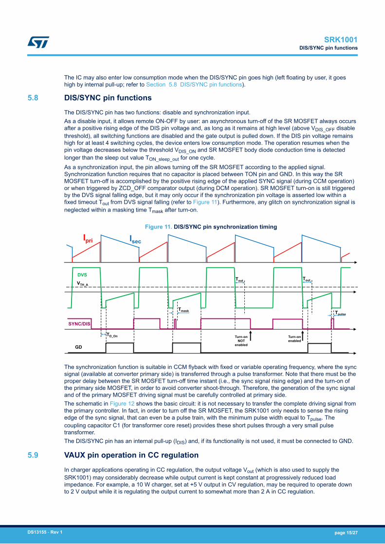
5.8 DIS/SYNC pin functions
The DIS/SYNC pin has two functions: disable and synchronization input.As a disable input, it allows remote ON-OFF by user: an asynchronous turn-off of the SR MOSFET always occursafter a positive rising edge of the DIS pin voltage and, as long as it remains at high level (above VDIS_OFF disablethreshold), all switching functions are disabled and the gate output is pulled down. If the DIS pin voltage remainshigh for at least 4 switching cycles, the device enters low consumption mode. The operation resumes when thepin voltage decreases below the threshold VDIS_ON and SR MOSFET body diode conduction time is detectedlonger than the sleep out value TON_sleep_out for one cycle.As a synchronization input, the pin allows turning off the SR MOSFET according to the applied signal.Synchronization function requires that no capacitor is placed between TON pin and GND. In this way the SRMOSFET turn-off is accomplished by the positive rising edge of the applied SYNC signal (during CCM operation)or when triggered by ZCD_OFF comparator output (during DCM operation). SR MOSFET turn-on is still triggeredby the DVS signal falling edge, but it may only occur if the synchronization pin voltage is asserted low within afixed timeout Tout from DVS signal falling (refer to Figure 11). Furthermore, any glitch on synchronization signal isneglected within a masking time Tmask after turn-on.
Figure 11. DIS/SYNC pin synchronization timing
Tmask
SYNC/DIS
Turn-onenabled
Turn-onNOT
enabled
TD_On
GD
VTH_ATout
DVS
IsecIpri
Tout
Tpulse
The synchronization function is suitable in CCM flyback with fixed or variable operating frequency, where the syncsignal (available at converter primary side) is transferred through a pulse transformer. Note that there must be theproper delay between the SR MOSFET turn-off time instant (i.e., the sync signal rising edge) and the turn-on ofthe primary side MOSFET, in order to avoid converter shoot-through. Therefore, the generation of the sync signaland of the primary MOSFET driving signal must be carefully controlled at primary side.The schematic in Figure 12 shows the basic circuit: it is not necessary to transfer the complete driving signal fromthe primary controller. In fact, in order to turn off the SR MOSFET, the SRK1001 only needs to sense the risingedge of the sync signal, that can even be a pulse train, with the minimum pulse width equal to Tpulse. Thecoupling capacitor C1 (for transformer core reset) provides these short pulses through a very small pulsetransformer.The DIS/SYNC pin has an internal pull-up (IDIS) and, if its functionality is not used, it must be connected to GND.
5.9 VAUX pin operation in CC regulation
In charger applications operating in CC regulation, the output voltage Vout (which is also used to supply theSRK1001) may considerably decrease while output current is kept constant at progressively reduced loadimpedance. For example, a 10 W charger, set at +5 V output in CV regulation, may be required to operate downto 2 V output while it is regulating the output current to somewhat more than 2 A in CC regulation.
SRK1001DIS/SYNC pin functions
DS13155 - Rev 1 page 15/27

Figure 12. Sync circuit with pulse transformer
In order to guarantee SR MOSFET switching even with low VCC supply voltage, the SRK1001 is provided with theVAUX pin. Referring to the schematic in Figure 13, when the VCC voltage decreases below the thresholdVCC_SO_On (> VCC_Off), an internal switch is turned on allowing the capacitor C2 placed on VCC pin to be chargedup to the turn-on threshold VCC_On by a current drawn through VAUX pin.
Figure 13. VAUX supply for CC regulation operation (from rectified SR MOSFET drain)
VCC_SO_On
Vin
D2 D1
C2 C1
Rext
SR-MOS
MOS
Cin Cout
NP NS
SW
DVS
VAUX
VCC
SO_COMP
VOUT
The VAUX pin may be connected, for example, to the rectified SR MOSFET drain voltage, like in Figure 13, or toanother auxiliary voltage of the flyback transformer, as shown in Figure 14.In either case, a (schottky) decoupling diode (D2) is necessary to avoid the VAUX pin charging the outputcapacitor. An external resistor Rext may be used in series with the VAUX pin in order to externally dissipate someof the power that, without that resistor, would be totally dissipated inside the SRK1001.
5.9.1 Example for parameter calculationsConsidering the circuit in Figure 13, the following example is provided to calculate the value of the Rext resistorand power dissipation, in the case of a +5 V charger with operation down to 2 V in CC regulation and transformersecondary-to-primary reflected voltage of 75 V.
SRK1001VAUX pin operation in CC regulation
DS13155 - Rev 1 page 16/27

Figure 14. VAUX supply for CC regulation operation from auxiliary winding
SR-MOSMOS
Cin CoutD2 D1
C2 C1
Rext
VCC_SO_On
SW
DVS
VAUX
VCC
Vin
SO_COMP
VOUT
Step 1. Measure or estimate the IC current consumption during CC regulation operation as below:ICC = Iq_run+ VCC_avg*Ciss*Fsw = 0.7mA+ 4.1V*5nF*50kHz = 1.725mAwhere Iq is the IC quiescent current, Vcc_avg is the average voltage across VCC pin (mean valuebetween VCC_On and VCC_SO_On), Ciss is the SR MOSFET input capacitance and Fsw is the operatingfrequency.
Step 2. Calculate the maximum and minimum voltage available at VAUX pin:VAUX_min = Vo .CC+ Vin .min NSNP − VF = 2V+ 75V 115 − 0.35V = 6.65VVAUX_max = Vo .CC+ Vin .max NSNP − VF = 2V+ 375V 115 − 0.35V = 26.65V
where Vo.CC is the output voltage in CC regulation, Vin.min / Vin.max is the converter minimum/maximuminput dc voltage, NS/NP is the transformer turn ratio, and VF is the voltage drop of D1.
Step 3. Calculate the power dissipation of SRK1001, including device consumption and driving:Pd_CC = Vcc_avg*ICC = 4.1V*1.725mA = 7.072mWwhere VCC_avg is the mean value between VCC_On and VCC_SO_On.
Step 4. Calculate the maximum external resistance in series to VAUX pin:Rext_MAX = VAUX_min − VCC_OnICC − Ron = 6.65V − 4.3V1.725mA − 40Ω = 1.322kΩRtot = Rext+ Ron = 1.2kΩ + 40Ω = 1.24kΩwhere Ron is the resistance of the internal VAUX switch.
Step 5. Calculate the maximum and minimum current from VAUX pin:IAUX_min = VAUX_min − VCC_OnRtot = 6.65V − 4.3V1.24kΩ = 1.89mAIAUX_max = VAUX_max − VCC_OnRtot = 26.65V − 4.3V1.24kΩ = 18.02mAStep 6. Calculate the maximum power dissipation from VAUX at maximum input voltage (Vin.max):Pd_AUX = VAUX_max*ICC = 26.65V*1.725mA = 45.971mW
SRK1001VAUX pin operation in CC regulation
DS13155 - Rev 1 page 17/27
Step 7. Calculate the maximum power dissipation on external resistance and inside SRK1001:
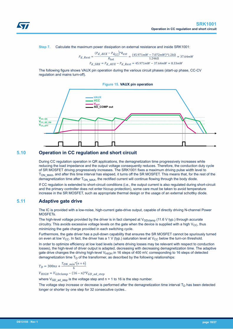
Pd_Rext = Pd_AUX − PdCC *RextRtot = 45.971mW− 7.072mW *1.2kΩ1.24kΩ = 37.64mWPd_SRK = Pd_AUX − Pd_Rext = 45.971mW− 37.64mW = 8.33mWThe following figure shows VAUX pin operation during the various circuit phases (start-up phase, CC-CVregulation and mains turn-off).
Figure 15. VAUX pin operation
VAUX
VCC_ON
VOUTSO_COMP out
VCC_OFF
VCC_SO_ON
VCC
5.10 Operation in CC regulation and short circuit
During CC regulation operation in QR applications, the demagnetization time progressively increases whilereducing the load impedance and the output voltage consequently reduces. Therefore, the conduction duty cycleof SR MOSFET driving progressively increases. The SRK1001 fixes a maximum driving pulse width level toTON_MAX, and after this time interval has elapsed, it turns off the SR MOSFET. This means that, for the rest of thedemagnetization time after TON_MAX, the rectified current will continue flowing through the body diode.If CC regulation is extended to short-circuit conditions (i.e., the output current is also regulated during short-circuitand the primary controller does not enter hiccup protection), some care must be taken to avoid temperatureincrease in the SR MOSFET, such as appropriate thermal design or the usage of an external schottky diode.
5.11 Adaptive gate drive
The IC is provided with a low-noise, high-current gate-drive output, capable of directly driving N-channel PowerMOSFETs.The high-level voltage provided by the driver is in fact clamped at VGDclamp (11.6 V typ.) through accuratecircuitry. This avoids excessive voltage levels on the gate when the device is supplied with a high VCC, thusminimizing the gate charge provided in each switching cycle.Furthermore, the gate driver has a pull-down capability that ensures the SR MOSFET cannot be spuriously turnedon even at low VCC. In fact, the driver has a 1 V (typ.) saturation level at VCC below the turn-on threshold.In order to optimize efficiency at low load levels (where driving losses may be relevant with respect to conductionlosses), the high-level of driver output is adapted, decreasing with decreasing demagnetization time. The adaptivegate drive changes the driving high-level VHIGH in 16 steps of 400 mV, corresponding to 16 steps of detecteddemagnetization time TD of the transformer, as described by the following relationships:TD = 300ns+ TON_min* n+ 66VHIGH = VGDclamp – 16 – n *VGD_ad_stepwhere VGD_ad_step is the voltage step and n = 1 to 16 is the step number.The voltage step increase or decrease is performed after the demagnetization time interval TD has been detectedlonger or shorter by one step for 32 consecutive cycles..
SRK1001Operation in CC regulation and short circuit
DS13155 - Rev 1 page 18/27
The driver voltage level VHIGH is limited by the supply voltage on VCC pin and, in any case, when VCC voltagesupply is detected lower than a threshold, the driver high-level modulation is disabled. A comparator withhysteresis enables adaptive drive when VCC supply increases above VCC_AGD_en and disables it as VCC fallsbelow VCC_AGD_dis. This means that if the VCC supply is low (but higher than VCC_AGD_dis), the driver high-levelVHIGH will be the minimum between the value of above formula and a value equal to:• VCC supply if VAUX function is used (and VAUX pin voltage is larger than VCC - 1.2V), or• VCC - 1.2 V if VAUX function is not used.
The adaptive gate drive is also disabled when the circuit enters burst-mode operation. On resuming operationfrom burst-mode, the gate drive always starts from the highest level and then it begins adapting the levelaccording to the sensed demagnetization period.In sleep-mode, the behavior is different. When the load (after entering sleep-mode) increases and the SRK1001controller resumes switching, the gate drive starts from the lower level and then progressively adapts with stepVGD_ad_step according to the sensed demagnetization period. The same also happens when the SRK1001 deviceexits the low-consumption state by DIS-SYNC pin. Also in this case, the gate drive starts from the lower level andthen begins adapting with step VGD_ad_step according to the sensed demagnetization period.Generally speaking, an SR MOSFET is always switched on after current starts flowing through its body diodewhen the drain-source voltage is already low (equal to VF). Therefore, there is no Miller effect or switching lossesat MOSFET turn-on. This is true also at turn-off, since rectifier current after the SR MOSFET is switched offcontinues flowing into the body diode. Consequently, the required gate charge the driver has to provide eachcycle for ON/OFF switching is rather lower than in case of hard switching and can be easily determined fromMOSFET datasheets in order to calculate the driver power dissipation.
SRK1001Adaptive gate drive
DS13155 - Rev 1 page 19/27

6 Layout guidelines
The GND pin is the return of the bias current of the device and return for gate drive current. It should be routedalong the shortest route possible to the common point where the source terminal of the SR MOSFET and outputcapacitor negative terminal are connected. When laying out the PCB, keep the source terminal of the SRMOSFET as close to output capacitor negative terminal as possible.DVS connection to SR MOSFET drain terminal is not critical (since adaptive turn-off algorithm automaticallycompensates for stray inductances in the SR MOSFET current path). Nevertheless, it is preferable to sense theMOSFET voltage as close to its drain terminal as possible.The usage of bypass capacitors between the VCC pin and GND pin is recommended. They should be low-ESR,low-ESL type and located as close to the IC pins as possible. Sometimes, a series resistor (in the tens of Ohms)between the converter output voltage and the VCC pin, forming an RC filter along with the bypass capacitor, isuseful to obtain a cleaner VCC voltage.Since the TON pin and TOFF pin source current is relatively low, this pin may be affected by current injectionscoming from nearby tracks with high dV/dt (i.e., drain sense signals). Therefore, TON pin and TOFF pin should bekept away from SR MOSFET drain tracks. In case of large noise, a capacitor can be used on these pins forfiltering. For the TOFF pin, the allowed capacitance COFF is such that the time constant ROFF COFF is lower than100 µs. For the TON pin, as it is also used for internal timer setting according to user selected operation (quasi-resonant or fixed frequency), the allowed capacitance CON is as follows:• Max. 22 pF for quasi-resonant operation• Min. 100 pF and time constant RON CON < 100 µs for fixed frequency operation
In applications where high noise is present on the sensed DVS signal (especially after the SR MOSFET turn-offinstant with a non-optimized layout or coupling with other asynchronous noise sources), some RC filtering on theDVS pin may help avoid undesirable device operation.
SRK1001Layout guidelines
DS13155 - Rev 1 page 20/27

7 Package mechanical data
Table 5. SO8 mechanical data
Dimensions
Ref.mm inch
Min Typ Max Min Typ Max
A 1.35 1.75 0.053 0.069
A1 0.10 0.25 0.004 0.010
A2 1.10 1.65 0.043 0.065
B 0.33 0.51 0.013 0.020
C 0.19 0.25 0.007 0.010
D (1) 4.80 5.00 0.189 0.197
E 3.80 4.00 0.150 0.157
e 1.27
H 5.8 6.20 0.228 0.050 0.244
h 0.25 0.50 0.010 0.020
L 0.40 1.27 0.016 0.050
k 0° (min), 8° (max)
ddd 0.10 0.004
1. D dimensions do not include mold flash, protrusions or gate burrs. Mold flash, protrusions or gate burrs should not exceed0.15 mm (0.006 inch) in total (both sides)
SRK1001Package mechanical data
DS13155 - Rev 1 page 21/27

Figure 16. SO8 package outline
SRK1001Package mechanical data
DS13155 - Rev 1 page 22/27

Revision history
Table 6. Document revision history
Date Version Changes
29-Nov-2019 1 Initial release.
SRK1001
DS13155 - Rev 1 page 23/27

Contents
1 Block diagram and pin connection . . . . . . . . . . . . . . . . . . . . . . . . . . . . . . . . . . . . . . . . . . . . . . . . .2
2 Maximum ratings . . . . . . . . . . . . . . . . . . . . . . . . . . . . . . . . . . . . . . . . . . . . . . . . . . . . . . . . . . . . . . . . . .4
3 Typical application schematic. . . . . . . . . . . . . . . . . . . . . . . . . . . . . . . . . . . . . . . . . . . . . . . . . . . . . .5
4 Electrical characteristics. . . . . . . . . . . . . . . . . . . . . . . . . . . . . . . . . . . . . . . . . . . . . . . . . . . . . . . . . . .6
5 Operation description. . . . . . . . . . . . . . . . . . . . . . . . . . . . . . . . . . . . . . . . . . . . . . . . . . . . . . . . . . . . . .9
5.1 Drain voltage sensing . . . . . . . . . . . . . . . . . . . . . . . . . . . . . . . . . . . . . . . . . . . . . . . . . . . . . . . . . . 10
5.2 Turn-on . . . . . . . . . . . . . . . . . . . . . . . . . . . . . . . . . . . . . . . . . . . . . . . . . . . . . . . . . . . . . . . . . . . . . . 10
5.3 Minimum TON programming. . . . . . . . . . . . . . . . . . . . . . . . . . . . . . . . . . . . . . . . . . . . . . . . . . . . . 10
5.4 Adaptive turn-off and TIMER . . . . . . . . . . . . . . . . . . . . . . . . . . . . . . . . . . . . . . . . . . . . . . . . . . . . 10
5.4.1 Fixed frequency mixed DCM/CCM operation . . . . . . . . . . . . . . . . . . . . . . . . . . . . . . . . . . 11
5.4.2 QR operation (with valley skipping) . . . . . . . . . . . . . . . . . . . . . . . . . . . . . . . . . . . . . . . . . . 12
5.4.3 Fixed frequency DCM operation . . . . . . . . . . . . . . . . . . . . . . . . . . . . . . . . . . . . . . . . . . . . 12
5.4.4 Variable frequency CCM operation . . . . . . . . . . . . . . . . . . . . . . . . . . . . . . . . . . . . . . . . . . 13
5.5 Minimum TOFF programming . . . . . . . . . . . . . . . . . . . . . . . . . . . . . . . . . . . . . . . . . . . . . . . . . . . . 13
5.6 Start-up phase . . . . . . . . . . . . . . . . . . . . . . . . . . . . . . . . . . . . . . . . . . . . . . . . . . . . . . . . . . . . . . . . 14
5.7 Low consumption mode operation: sleep-mode, burst mode, disable state . . . . . . . . . . . . . 14
5.8 DIS/SYNC pin functions . . . . . . . . . . . . . . . . . . . . . . . . . . . . . . . . . . . . . . . . . . . . . . . . . . . . . . . . 15
5.9 VAUX pin operation in CC regulation . . . . . . . . . . . . . . . . . . . . . . . . . . . . . . . . . . . . . . . . . . . . . 15
5.9.1 Example for parameter calculations . . . . . . . . . . . . . . . . . . . . . . . . . . . . . . . . . . . . . . . . . 16
5.10 Operation in CC regulation and short circuit . . . . . . . . . . . . . . . . . . . . . . . . . . . . . . . . . . . . . . . 18
5.11 Adaptive gate drive . . . . . . . . . . . . . . . . . . . . . . . . . . . . . . . . . . . . . . . . . . . . . . . . . . . . . . . . . . . . 18
6 Layout guidelines. . . . . . . . . . . . . . . . . . . . . . . . . . . . . . . . . . . . . . . . . . . . . . . . . . . . . . . . . . . . . . . . .20
7 Package mechanical data . . . . . . . . . . . . . . . . . . . . . . . . . . . . . . . . . . . . . . . . . . . . . . . . . . . . . . . . .21
Revision history . . . . . . . . . . . . . . . . . . . . . . . . . . . . . . . . . . . . . . . . . . . . . . . . . . . . . . . . . . . . . . . . . . . . . . .23
SRK1001Contents
DS13155 - Rev 1 page 24/27
List of figuresFigure 1. Internal block diagram . . . . . . . . . . . . . . . . . . . . . . . . . . . . . . . . . . . . . . . . . . . . . . . . . . . . . . . . . . . . . . . 2Figure 2. Pin connections (top view) . . . . . . . . . . . . . . . . . . . . . . . . . . . . . . . . . . . . . . . . . . . . . . . . . . . . . . . . . . . . 2Figure 3. Typical application schematic . . . . . . . . . . . . . . . . . . . . . . . . . . . . . . . . . . . . . . . . . . . . . . . . . . . . . . . . . . 5Figure 4. Rise and fall time definition. . . . . . . . . . . . . . . . . . . . . . . . . . . . . . . . . . . . . . . . . . . . . . . . . . . . . . . . . . . . 8Figure 5. Comparison between adaptive turn-off and comparator based turn-off . . . . . . . . . . . . . . . . . . . . . . . . . . . . . 10Figure 6. ZCD_OFF threshold adapting for target body diode conduction. . . . . . . . . . . . . . . . . . . . . . . . . . . . . . . . . . 11Figure 7. Timer anticipation for fixed frequency CCM operation (100pF mounted on TON pin) . . . . . . . . . . . . . . . . . . . 12Figure 8. Timer anticipation for QR operating circuit (no capacitor mounted on TON pin) . . . . . . . . . . . . . . . . . . . . . . . 12Figure 9. Blanking time after turn-off . . . . . . . . . . . . . . . . . . . . . . . . . . . . . . . . . . . . . . . . . . . . . . . . . . . . . . . . . . . 13Figure 10. Comparator for blanking time termination . . . . . . . . . . . . . . . . . . . . . . . . . . . . . . . . . . . . . . . . . . . . . . . . . 14Figure 11. DIS/SYNC pin synchronization timing . . . . . . . . . . . . . . . . . . . . . . . . . . . . . . . . . . . . . . . . . . . . . . . . . . . 15Figure 12. Sync circuit with pulse transformer . . . . . . . . . . . . . . . . . . . . . . . . . . . . . . . . . . . . . . . . . . . . . . . . . . . . . 16Figure 13. VAUX supply for CC regulation operation (from rectified SR MOSFET drain) . . . . . . . . . . . . . . . . . . . . . . . . 16Figure 14. VAUX supply for CC regulation operation from auxiliary winding . . . . . . . . . . . . . . . . . . . . . . . . . . . . . . . . . 17Figure 15. VAUX pin operation. . . . . . . . . . . . . . . . . . . . . . . . . . . . . . . . . . . . . . . . . . . . . . . . . . . . . . . . . . . . . . . . 18Figure 16. SO8 package outline . . . . . . . . . . . . . . . . . . . . . . . . . . . . . . . . . . . . . . . . . . . . . . . . . . . . . . . . . . . . . . . 22
SRK1001List of figures
DS13155 - Rev 1 page 25/27

List of tablesTable 1. Pin functions . . . . . . . . . . . . . . . . . . . . . . . . . . . . . . . . . . . . . . . . . . . . . . . . . . . . . . . . . . . . . . . . . . . . . . . 2Table 2. Absolute maximum ratings . . . . . . . . . . . . . . . . . . . . . . . . . . . . . . . . . . . . . . . . . . . . . . . . . . . . . . . . . . . . . 4Table 3. Thermal data. . . . . . . . . . . . . . . . . . . . . . . . . . . . . . . . . . . . . . . . . . . . . . . . . . . . . . . . . . . . . . . . . . . . . . . 4Table 4. Electrical characteristics . . . . . . . . . . . . . . . . . . . . . . . . . . . . . . . . . . . . . . . . . . . . . . . . . . . . . . . . . . . . . . . 6Table 5. SO8 mechanical data . . . . . . . . . . . . . . . . . . . . . . . . . . . . . . . . . . . . . . . . . . . . . . . . . . . . . . . . . . . . . . . . 21Table 6. Document revision history . . . . . . . . . . . . . . . . . . . . . . . . . . . . . . . . . . . . . . . . . . . . . . . . . . . . . . . . . . . . . 23
SRK1001List of tables
DS13155 - Rev 1 page 26/27

IMPORTANT NOTICE – PLEASE READ CAREFULLY
STMicroelectronics NV and its subsidiaries (“ST”) reserve the right to make changes, corrections, enhancements, modifications, and improvements to STproducts and/or to this document at any time without notice. Purchasers should obtain the latest relevant information on ST products before placing orders. STproducts are sold pursuant to ST’s terms and conditions of sale in place at the time of order acknowledgement.
Purchasers are solely responsible for the choice, selection, and use of ST products and ST assumes no liability for application assistance or the design ofPurchasers’ products.
No license, express or implied, to any intellectual property right is granted by ST herein.
Resale of ST products with provisions different from the information set forth herein shall void any warranty granted by ST for such product.
ST and the ST logo are trademarks of ST. For additional information about ST trademarks, please refer to www.st.com/trademarks. All other product or servicenames are the property of their respective owners.
Information in this document supersedes and replaces information previously supplied in any prior versions of this document.
© 2019 STMicroelectronics – All rights reserved
SRK1001
DS13155 - Rev 1 page 27/27